JP7657631B2 - EVALUATION APPARATUS, PROGRAM, EVALUATION METHOD, MOLDING SYSTEM, AND ARTICLE MANUFACTURING METHOD - Google Patents
EVALUATION APPARATUS, PROGRAM, EVALUATION METHOD, MOLDING SYSTEM, AND ARTICLE MANUFACTURING METHODDownload PDFInfo
- Publication number
- JP7657631B2 JP7657631B2JP2021055838AJP2021055838AJP7657631B2JP 7657631 B2JP7657631 B2JP 7657631B2JP 2021055838 AJP2021055838 AJP 2021055838AJP 2021055838 AJP2021055838 AJP 2021055838AJP 7657631 B2JP7657631 B2JP 7657631B2
- Authority
- JP
- Japan
- Prior art keywords
- substrate
- image
- mold
- abnormality
- evaluation device
- Prior art date
- Legal status (The legal status is an assumption and is not a legal conclusion. Google has not performed a legal analysis and makes no representation as to the accuracy of the status listed.)
- Active
Links
Images


Classifications
- G—PHYSICS
- G03—PHOTOGRAPHY; CINEMATOGRAPHY; ANALOGOUS TECHNIQUES USING WAVES OTHER THAN OPTICAL WAVES; ELECTROGRAPHY; HOLOGRAPHY
- G03F—PHOTOMECHANICAL PRODUCTION OF TEXTURED OR PATTERNED SURFACES, e.g. FOR PRINTING, FOR PROCESSING OF SEMICONDUCTOR DEVICES; MATERIALS THEREFOR; ORIGINALS THEREFOR; APPARATUS SPECIALLY ADAPTED THEREFOR
- G03F7/00—Photomechanical, e.g. photolithographic, production of textured or patterned surfaces, e.g. printing surfaces; Materials therefor, e.g. comprising photoresists; Apparatus specially adapted therefor
- G03F7/0002—Lithographic processes using patterning methods other than those involving the exposure to radiation, e.g. by stamping
- G—PHYSICS
- G03—PHOTOGRAPHY; CINEMATOGRAPHY; ANALOGOUS TECHNIQUES USING WAVES OTHER THAN OPTICAL WAVES; ELECTROGRAPHY; HOLOGRAPHY
- G03F—PHOTOMECHANICAL PRODUCTION OF TEXTURED OR PATTERNED SURFACES, e.g. FOR PRINTING, FOR PROCESSING OF SEMICONDUCTOR DEVICES; MATERIALS THEREFOR; ORIGINALS THEREFOR; APPARATUS SPECIALLY ADAPTED THEREFOR
- G03F7/00—Photomechanical, e.g. photolithographic, production of textured or patterned surfaces, e.g. printing surfaces; Materials therefor, e.g. comprising photoresists; Apparatus specially adapted therefor
- G03F7/70—Microphotolithographic exposure; Apparatus therefor
- G03F7/70483—Information management; Active and passive control; Testing; Wafer monitoring, e.g. pattern monitoring
- G03F7/70605—Workpiece metrology
- G03F7/70616—Monitoring the printed patterns
- G03F7/7065—Defects, e.g. optical inspection of patterned layer for defects
- G—PHYSICS
- G03—PHOTOGRAPHY; CINEMATOGRAPHY; ANALOGOUS TECHNIQUES USING WAVES OTHER THAN OPTICAL WAVES; ELECTROGRAPHY; HOLOGRAPHY
- G03F—PHOTOMECHANICAL PRODUCTION OF TEXTURED OR PATTERNED SURFACES, e.g. FOR PRINTING, FOR PROCESSING OF SEMICONDUCTOR DEVICES; MATERIALS THEREFOR; ORIGINALS THEREFOR; APPARATUS SPECIALLY ADAPTED THEREFOR
- G03F9/00—Registration or positioning of originals, masks, frames, photographic sheets or textured or patterned surfaces, e.g. automatically
- G03F9/70—Registration or positioning of originals, masks, frames, photographic sheets or textured or patterned surfaces, e.g. automatically for microlithography
- G03F9/7003—Alignment type or strategy, e.g. leveling, global alignment
- G03F9/7042—Alignment for lithographic apparatus using patterning methods other than those involving the exposure to radiation, e.g. by stamping or imprinting
- G—PHYSICS
- G06—COMPUTING OR CALCULATING; COUNTING
- G06N—COMPUTING ARRANGEMENTS BASED ON SPECIFIC COMPUTATIONAL MODELS
- G06N20/00—Machine learning
- G—PHYSICS
- G06—COMPUTING OR CALCULATING; COUNTING
- G06T—IMAGE DATA PROCESSING OR GENERATION, IN GENERAL
- G06T7/00—Image analysis
- G06T7/0002—Inspection of images, e.g. flaw detection
- G06T7/0004—Industrial image inspection
- G—PHYSICS
- G06—COMPUTING OR CALCULATING; COUNTING
- G06T—IMAGE DATA PROCESSING OR GENERATION, IN GENERAL
- G06T2207/00—Indexing scheme for image analysis or image enhancement
- G06T2207/20—Special algorithmic details
- G06T2207/20081—Training; Learning
- G—PHYSICS
- G06—COMPUTING OR CALCULATING; COUNTING
- G06T—IMAGE DATA PROCESSING OR GENERATION, IN GENERAL
- G06T2207/00—Indexing scheme for image analysis or image enhancement
- G06T2207/20—Special algorithmic details
- G06T2207/20084—Artificial neural networks [ANN]
- G—PHYSICS
- G06—COMPUTING OR CALCULATING; COUNTING
- G06T—IMAGE DATA PROCESSING OR GENERATION, IN GENERAL
- G06T2207/00—Indexing scheme for image analysis or image enhancement
- G06T2207/30—Subject of image; Context of image processing
- G06T2207/30108—Industrial image inspection
- G06T2207/30148—Semiconductor; IC; Wafer
Landscapes
- Engineering & Computer Science (AREA)
- Physics & Mathematics (AREA)
- General Physics & Mathematics (AREA)
- Theoretical Computer Science (AREA)
- Computer Vision & Pattern Recognition (AREA)
- Software Systems (AREA)
- Quality & Reliability (AREA)
- Data Mining & Analysis (AREA)
- Evolutionary Computation (AREA)
- Medical Informatics (AREA)
- Computing Systems (AREA)
- General Engineering & Computer Science (AREA)
- Mathematical Physics (AREA)
- Artificial Intelligence (AREA)
- Exposure Of Semiconductors, Excluding Electron Or Ion Beam Exposure (AREA)
- Shaping Of Tube Ends By Bending Or Straightening (AREA)
Description
Translated fromJapanese本発明は、評価装置、プログラム、評価方法、成形システム、および物品製造方法に関する。The present invention relates to an evaluation device, a program, an evaluation method, a molding system, and an article manufacturing method.
ナノメートルオーダーのデザインルールによる微細構造デバイスの生産が可能で、かつ大量生産向きである技術として、インプリント技術の実用化が進んでいる。インプリント技術は、電子線描画装置や露光装置等を用いて製作されたナノメートルスケールの凹凸構造のパターンを持つ型(モールド、テンプレートとも呼ばれる。)を、基板上の成形可能材料(インプリント材)に接触させてパターンを転写する技術である。インプリント技術の一つとして、例えば、光硬化法がある。光硬化法を採用したインプリント装置は、基板上のショット領域に供給された光硬化性のインプリント材を型で成形し、光を照射してインプリント材を硬化させ、硬化したインプリント材から型を引き離すことで、基板上にパターンを形成する。Imprint technology is being put to practical use as a technology that allows for the production of microstructure devices according to nanometer-order design rules and is suitable for mass production. Imprint technology involves contacting a mold (also called a template) with a nanometer-scale uneven structure pattern produced using an electron beam lithography device or exposure device with a moldable material (imprint material) on a substrate to transfer the pattern. One imprint technology is, for example, the photocuring method. An imprint device that employs the photocuring method forms a photocurable imprint material supplied to a shot area on a substrate with a mold, irradiates light to harden the imprint material, and forms a pattern on the substrate by separating the mold from the hardened imprint material.
インプリント技術を用いて基板上にパターンを形成する際に、インプリント材がショット領域外にはみ出す浸み出しが発生する場合がある。逆に、インプリント材が行き渡らずに部分的にパターンを形成できない未充填が発生する場合もある。浸み出しが発生すると、インプリント材がはみ出した箇所が不良となるとともに、インプリント材がはみ出した先のショット領域にパターンを形成する際に、はみ出したインプリント材と型とが接触して型のパターンが破損してしまう可能性がある。また、未充填が発生すると、ショット領域上に部分的にパターンが形成されていないため、半導体デバイスとして不良となる可能性がある。When forming a pattern on a substrate using imprint technology, seepage may occur, where the imprint material spills out of the shot area. Conversely, underfilling may occur, where the imprint material does not spread thoroughly and a pattern cannot be formed in some areas. When seepage occurs, the area where the imprint material spills out may become defective, and when a pattern is formed in the shot area beyond the spilled imprint material, the spilled imprint material may come into contact with the mold, damaging the pattern on the mold. Furthermore, underfilling may result in a defective semiconductor device, as a pattern is not formed in parts of the shot area.
そこで、インプリント処理の後に浸み出しや未充填の有無を観察(確認)し、基板上に供給するインプリント材の量や位置を調整して、浸み出しや未充填の発生を抑える必要がある。浸み出しや未充填が発生している箇所は微小な領域であるため、観察範囲が狭く、高倍率の顕微鏡で得られた膨大な数の観察画像を確認する必要があるが、このような膨大な数の観察画像を人が確認することは現実的ではない。従って、人手を介さずに、観察画像から浸み出しや未充填を検査して、浸み出しや未充填に起因するパターンの異常(形成不良)を判定する技術が要求されている。Therefore, after the imprint process, it is necessary to observe (confirm) the presence or absence of seepage or non-filling, and adjust the amount and position of the imprint material supplied onto the substrate to prevent seepage or non-filling from occurring. Because the areas where seepage or non-filling occurs are tiny regions, the observation range is narrow and it is necessary to check a huge number of observation images obtained with a high-magnification microscope, but it is not realistic for a person to check such a huge number of observation images. Therefore, there is a demand for technology that can inspect the observation images for seepage or non-filling without human intervention, and determine pattern abnormalities (formation defects) caused by seepage or non-filling.
パターンの形成不良にはさまざまな種類やサイズなどの特徴が存在し、形成不良の特徴によってプロセスに与える影響や対策が異なるため、それら特徴を区別することが必要である。また、画像が撮影された場所などの、画像情報以外の情報によって、形成不良に対する処理が異なる場合もある。Pattern defects come in a variety of types, sizes, and other characteristics, and since the impact they have on the process and the measures they require vary depending on the characteristics of the defect, it is necessary to distinguish between these characteristics. In addition, the way in which defects are dealt with may differ depending on information other than image information, such as the location where the image was taken.
本発明は、成形処理によって得られた基板上の組成物の異常の検出および種類を高効率に確認するのに有利な技術を提供する。The present invention provides an advantageous technology for efficiently detecting and identifying the type of anomalies in a composition on a substrate obtained by a molding process.
本発明の一側面によれば、成形処理によって基板の上に形成された組成物を評価する評価装置であって、前記成形処理は、前記基板のショット領域上の成形可能材料と型とを接触させた状態で該成形可能材料を硬化させることによって、前記基板の上に前記成形可能材料の硬化物からなる前記組成物を形成する処理であり、前記評価装置は、前記成形処理によって前記基板の上に形成された前記組成物を含む画像を取得する取得部と、前記取得された画像を前記評価のために処理する処理部と、を有し、前記処理部は、前記取得された画像における異常の位置とサイズを推論モデルに従い出力し、前記ショット領域におけるデバイス領域と非デバイス領域との境界と、前記異常の前記位置および前記サイズとの関係に基づいて、前記異常の種類の判定を行い、前記判定の結果に基づいて、前記画像が正常な画像であるか異常を含む画像であるかの最終判定を行う、ことを特徴とする評価装置が提供される。 According to one aspect of the present invention, there is provided an evaluation device for evaluating a composition formed on a substrate by a molding process, the molding process being a process for forming the composition consisting of a hardened product of the moldable material on the substrate by hardening the moldable material ona shot region of the substrate while the mold is in contact with the mold, the evaluation device having an acquisition unit that acquires an image including the composition formed on the substrate by the molding process, and a processing unit that processes the acquired image for the evaluation, the processing unit outputtingthe position and size of an anomaly in the acquired image according to an inference model, determining thetypeof the anomaly based on the relationship between the boundary between a device region and a non-device region in the shot region and the position and the size of the anomaly, and making a final determination as to whether the image is a normal image or an image including an anomaly based on the result of the determination.
本発明によれば、成形処理によって得られた基板上の組成物の異常の検出および種類を高効率に確認するのに有利な技術を提供することができる。The present invention provides a technology that is advantageous for efficiently detecting and identifying the type of abnormality in a composition on a substrate obtained by a molding process.
以下、添付図面を参照して実施形態を詳しく説明する。なお、以下の実施形態は特許請求の範囲に係る発明を限定するものではない。実施形態には複数の特徴が記載されているが、これらの複数の特徴の全てが発明に必須のものとは限らず、また、複数の特徴は任意に組み合わせられてもよい。さらに、添付図面においては、同一若しくは同様の構成に同一の参照番号を付し、重複した説明は省略する。The following embodiments are described in detail with reference to the attached drawings. Note that the following embodiments do not limit the invention according to the claims. Although the embodiments describe multiple features, not all of these multiple features are necessarily essential to the invention, and multiple features may be combined in any manner. Furthermore, in the attached drawings, the same reference numbers are used for the same or similar configurations, and duplicate explanations are omitted.
以下の実施形態は、基板の上の成形可能材料(硬化性組成物)を成形する成形処理を行う成形装置を含む成形システムに関するものである。成形処理は、基板の上に供給された成形可能材料と型(原版、テンプレート)とを接触させる接触工程を含む。この接触によって成形可能材料が成形される。成形処理は更に、成形可能材料と型とが接触した状態で成形可能材料を硬化させる硬化工程を含みうる。これにより、基板の上に成形可能材料の硬化物からなる組成物が形成される。成形処理は更に、成形可能材料の硬化物からなる組成物と型とを分離する離型工程とを含みうる。The following embodiment relates to a molding system including a molding device that performs a molding process to mold a moldable material (curable composition) on a substrate. The molding process includes a contacting step of bringing the moldable material supplied on the substrate into contact with a mold (original plate, template). This contact molds the moldable material. The molding process may further include a curing step of curing the moldable material while the moldable material is in contact with the mold. This forms a composition made of a cured product of the moldable material on the substrate. The molding process may further include a demolding step of separating the composition made of a cured product of the moldable material from the mold.
成形装置は、基板上のパターンを形成すべきショット領域の上に供給された成形可能材料であるインプリント材と型のパターン部との接触を行うことによって型のパターンをインプリント材に転写するインプリント装置として使用することができる。パターンは、例えば、半導体デバイスのパターン(デバイスパターン)でありうる。インプリント装置においては、基板に形成された複数のショット領域のそれぞれごとにインプリントを行うことができる。あるいは、インプリント装置は、基板の複数のショット領域について一括して(基板全面、または、1または2以上の列のショット領域の単位で)インプリント(すなわち、接触)を行う仕様にすることもできる。The molding device can be used as an imprinting device that transfers a pattern of a mold to an imprinting material, which is a moldable material supplied onto a shot area on a substrate where a pattern is to be formed, by contacting the imprinting material with a pattern portion of a mold. The pattern can be, for example, a semiconductor device pattern (device pattern). In the imprinting device, imprinting can be performed for each of a plurality of shot areas formed on the substrate. Alternatively, the imprinting device can be configured to imprint (i.e., contact) a plurality of shot areas of the substrate all at once (over the entire substrate, or in units of one or more rows of shot areas).
あるいは、成形装置は、基板の上の成形可能材料と平坦面を有する部材(型の平坦面)とを接触させることによって基板の上に成形可能材料による平坦化膜を形成する平坦化装置として使用することもできる。Alternatively, the molding device can be used as a planarizing device that forms a planarized film of moldable material on a substrate by contacting the moldable material on the substrate with a member having a flat surface (the flat surface of a mold).
以下では、具体例を示すため、成形装置の一例であるインプリント装置を含むシステムについて説明する。To provide a concrete example, we will explain below a system that includes an imprint device, which is an example of a molding device.
図1(a)には、実施形態におけるインプリント装置IMPの構成が模式的に示されている。インプリント装置IMPは、基板Sの上のインプリント材IMと型Mのパターン領域MPとを接触させた状態でインプリント材IMを硬化させ、インプリント材IMの硬化物と型Mとを分離するインプリント処理を行う。このインプリント処理によって、基板Sの上にインプリント材IMの硬化物からなるパターンが形成される。Figure 1(a) shows a schematic configuration of an imprint apparatus IMP in an embodiment. The imprint apparatus IMP performs an imprint process in which the imprint material IM on the substrate S is brought into contact with a pattern region MP of a mold M, the imprint material IM is cured, and the mold M is separated from the cured imprint material IM. This imprint process forms a pattern made of the cured imprint material IM on the substrate S.
インプリント材としては、硬化用のエネルギーが与えられることにより硬化する硬化性組成物(未硬化状態の樹脂と呼ぶこともある)が用いられる。硬化用のエネルギーとしては、電磁波、熱等が用いられうる。電磁波は、例えば、その波長が10nm以上1mm以下の範囲から選択される光、例えば、赤外線、可視光線、紫外線などでありうる。硬化性組成物は、光の照射により、あるいは、加熱により硬化する組成物でありうる。これらのうち、光の照射により硬化する光硬化性組成物は、少なくとも重合性化合物と光重合開始剤とを含有し、必要に応じて非重合性化合物または溶剤を更に含有してもよい。非重合性化合物は、増感剤、水素供与体、内添型離型剤、界面活性剤、酸化防止剤、ポリマー成分などの群から選択される少なくとも一種である。インプリント材は、液滴状、或いは複数の液滴が繋がってできた島状又は膜状となって基板上に配置されうる。インプリント材の粘度(25℃における粘度)は、例えば、1mPa・s以上100mPa・s以下でありうる。基板の材料としては、例えば、ガラス、セラミックス、金属、半導体、樹脂等が用いられうる。必要に応じて、基板の表面に、基板とは別の材料からなる部材が設けられてもよい。基板は、例えば、シリコンウエハ、化合物半導体ウエハ、石英ガラスである。As the imprint material, a curable composition (sometimes called an uncured resin) that is cured by applying energy for curing is used. As the energy for curing, electromagnetic waves, heat, etc. can be used. The electromagnetic waves can be, for example, light having a wavelength selected from the range of 10 nm to 1 mm, such as infrared rays, visible light, and ultraviolet rays. The curable composition can be a composition that is cured by irradiation with light or by heating. Among these, the photocurable composition that is cured by irradiation with light contains at least a polymerizable compound and a photopolymerization initiator, and may further contain a non-polymerizable compound or a solvent as necessary. The non-polymerizable compound is at least one selected from the group consisting of a sensitizer, a hydrogen donor, an internal mold release agent, a surfactant, an antioxidant, and a polymer component. The imprint material can be arranged on the substrate in the form of droplets, or in the form of islands or a film formed by connecting a plurality of droplets. The viscosity of the imprint material (at 25°C) can be, for example, 1 mPa·s to 100 mPa·s. Examples of materials that can be used for the substrate include glass, ceramics, metals, semiconductors, and resins. If necessary, a member made of a material different from that of the substrate may be provided on the surface of the substrate. The substrate may be, for example, a silicon wafer, a compound semiconductor wafer, or quartz glass.
本明細書および図面においては、水平面をXY平面とするXYZ座標系において方向が示される。一般には、基板Sはその表面が水平面(XY平面)と平行になるように基板保持部102の上に置かれる。よって以下では、基板Sの表面に沿う平面内で互いに直交する方向をX軸およびY軸とし、X軸およびY軸に垂直な方向をZ軸とする。また、以下では、XYZ座標系におけるX軸、Y軸、Z軸にそれぞれ平行な方向をX方向、Y方向、Z方向という。また、X軸周りの回転、Y軸周りの回転、Z軸周りの回転はそれぞれ、θX、θY、θZで示される。位置決めは、位置および/または姿勢を制御することを意味する。位置合わせは、基板および型の少なくとも一方の位置および/または姿勢の制御を含みうる。In this specification and the drawings, directions are indicated in an XYZ coordinate system with the horizontal plane as the XY plane. In general, the substrate S is placed on the
インプリント装置IMPは、基板Sを保持する基板保持部102、基板保持部102を駆動することによって基板Sを駆動する基板駆動機構105、基板保持部102を支持するベース104、基板保持部102の位置を計測する位置計測部103を備えうる。基板駆動機構105は、例えば、リニアモータ等のモータを含みうる。The imprint apparatus IMP may include a
インプリント装置IMPは、型(モールド)Mを保持する型保持部121、型保持部121を駆動することによって型Mを駆動する型駆動機構122、型駆動機構122を支持する支持構造体130を含みうる。型駆動機構122は、例えば、ボイスコイルモータ等のモータを含みうる。The imprint apparatus IMP may include a
基板駆動機構105および型駆動機構122は、基板Sと型Mとの相対位置および相対姿勢を調整する駆動機構を構成する。該駆動機構による基板Sと型Mとの相対位置の調整は、基板Sの上のインプリント材に対する型の接触、および、硬化したインプリント材(硬化物のパターン)からの型の分離のための駆動を含む。基板駆動機構105は、複数の自由度(例えば、X、Y、θZの3軸、好ましくは、X、Y、Z、θX、θY、θZの6軸)を持つ駆動機構でありうる。型駆動機構122も、複数の自由度(例えば、Z、θX、θYの3軸、好ましくは、X、Y、Z、θX、θY、θZの6軸)を持つ駆動機構でありうる。The
インプリント装置IMPは、型Mを搬送する型搬送機構140および型クリーナ150を備えうる。型搬送機構140は、例えば、型Mを型保持部121に搬送したり、型Mを型保持部121から原版ストッカ(不図示)または型クリーナ150等に搬送したりするように構成されうる。型クリーナ150は、型Mを紫外線や薬液等によってクリーニングする。The imprint apparatus IMP may include a
型保持部121は、型Mの裏面(基板Sに転写すべきパターンが形成されたパターン領域MPとは反対側の面)の側に圧力制御空間CSを形成する窓部材125を含みうる。インプリント装置IMPは、圧力制御空間CSの圧力(以下、キャビティ圧と呼ぶ)を制御することによって、図1(b)に模式的に示されるように、型Mのパターン領域MPを基板Sに向かって凸形状に変形させる変形機構123を備えうる。The
インプリント装置IMPは、アライメント計測器106、広角アライメント計測器151、硬化部107、撮像部112、光学部材111を備えうる。アライメント計測器106は、基板Sのアライメントマークと型Mのアライメントマークを照明するとともにその像を撮像することによりマーク間の相対位置を計測する。アライメント計測器106は、観察すべきアライメントマークの位置に応じて不図示の駆動機構によって位置決めされうる。広角アライメント計測器151は、アライメント計測器106より広い視野を有する計測器であり、基板Sのアライメントマークを照明するとともにその像を撮像することにより、基板Sの位置を計測する。広角アライメント計測器で基板Sの位置を計測することにより、アライメント計測器106の視野内に基板Sのアライメントマークを移動することができる。The imprint apparatus IMP may include an
硬化部107は、インプリント材IMを硬化させるためのエネルギー(例えば、紫外光等の光)を、光学部材111を介してインプリント材IMに照射し、これによりインプリント材IMを硬化させる。撮像部112は、光学部材111および窓部材125を介して基板S、型Mおよびインプリント材IMを撮像する。The
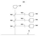
広角アライメント計測器151は、照明光の波長を切り換える機構を備えていてもよい。例えば、広角アライメント計測器151は、光路上に配置される波長フィルタを有し、波長フィルタの切り換えを行う機構を有する。あるいは、広角アライメント計測器151は、図2に示すように、同時に複数波長の画像を撮像できる構成を備えていてもよい。図2の計測器は、光源LS、光路と分岐する複数のハーフミラー162、それぞれ異なる波長を透過する複数の波長フィルタ163、複数の撮像素子164を含み、異なる波長の画像を同時に撮像できる。また、広角アライメント計測器151は、照明光の光量を切り換える機構を有していてもよい。例えば、広角アライメント計測器151は、光路にNDフィルタを配置し、NDフィルタの切り換えを行う機構も有する。また、広角アライメント計測器151は、明視野光学系および暗視野光学系等の複数の光学系を備え、撮像する像が通る光学系を切り換える機構を有していてもよい。また、広角アライメント計測器151は、照明光または受光の偏光を切り換える機構を備えていてもよい。例えば、光路に偏光フィルタを配置し、偏光フィルタの切り換えを行う機構も有する。The wide-angle
インプリント装置IMPは、基板Sの上にインプリント材IMを配置するディスペンサ108を備えうる。ディスペンサ108は、例えば、インプリント材IMの配置を示すドロップレシピに従ってインプリント材IMが基板Sの上に配置されるようにインプリント材IMを吐出する。インプリント装置IMPは、基板駆動機構105、型駆動機構122、変形機構123、型搬送機構140、型クリーナ150、アライメント計測器106、硬化部107、撮像部112、ディスペンサ108等を制御する制御部110を備えうる。制御部110は、例えば、FPGA(Field Programmable Gate Arrayの略。)などのPLD(Programmable Logic Deviceの略。)、又は、ASIC(Application Specific Integrated Circuitの略。)、又は、プログラムが組み込まれた汎用コンピュータ、又は、これらの全部または一部の組み合わせによって構成されうる。The imprint apparatus IMP may include a
図3には、半導体デバイス等の物品を製造するための物品製造システム401の構成が例示されている。物品製造システム401は、例えば、1または複数のインプリント装置IMPと、1または複数の検査装置405(例えば、重ね合わせ検査装置、CD検査装置、欠陥検査装置、電気特性検査装置)とを含みうる。また、物品製造システム401は、1または複数の基板処理装置406(エッチング装置、成膜装置)を含みうる。更に、物品製造システム401は、後述する評価装置407も含みうる。これらの装置は、ネットワーク402を介してインプリント装置IMPとは異なる外部装置である制御サーバ403と接続され、制御サーバ403によって制御されうる。Figure 3 illustrates an example of the configuration of an
評価装置407は、情報処理装置によって構成され、該情報処理装置は、例えば、FPGA(Field Programmable Gate Arrayの略。)などのPLD(Programmable Logic Deviceの略。)、又は、ASIC(Application Specific Integrated Circuitの略。)、又は、プログラムが組み込まれた汎用コンピュータ、又は、これらの全部または一部の組み合わせによって構成されうる。The
図14に、評価装置407の構成例を示す。評価装置407は、制御部4071と、一時的なデータを記憶するとともに制御部4071にワークエリアを提供するRAM4072と、固定的なデータおよびプログラムを記憶しているROM4073とを含みうる。評価装置407は更に、記憶装置4072と、表示装置4076と、入力装置4075とを含みうる。記憶装置4072には、本実施形態に係る評価方法を実行するためのプログラム4074aが記憶されている。ネットワークI/F4077は、ネットワーク402と接続するためのインタフェースである。本実施形態において、ネットワークI/F4077は、成形処理によって基板の上に形成された組成物を含む画像を取得する取得部として機能しうる。また、制御部4071は、取得された画像を評価のために処理する処理部として機能しうる。さらに、制御部4071は、表示部4076の表示を制御する表示制御部としても機能しうる。FIG. 14 shows an example of the configuration of the
なお、評価装置407は、インプリント装置IMPの制御部110、制御サーバ403、あるいは検査装置405等を用いて(併用して)実現されてもよい。インプリント装置IMPと評価装置407とを含むシステムは、成形システムあるいはリソグラフィシステムとして理解されてもよい。The
以下では、本実施形態に係るリソグラフィ方法について説明する。本実施形態では、インプリント処理を行った後に、パターンが形成されるべき領域であるショット領域およびその周辺を含む画像が撮像により取得される。この画像を用いて浸み出しおよび未充填が検出される。浸み出しおよび未充填を検出する際には、機械学習を用いる。また、機械学習では、物体検出アルゴリズムを用いることにより、異常の検出が実現されうる。The lithography method according to this embodiment will be described below. In this embodiment, after performing an imprint process, an image including a shot area, which is an area where a pattern is to be formed, and its surroundings is captured. This image is used to detect seepage and non-filling. Machine learning is used to detect seepage and non-filling. In machine learning, an object detection algorithm can be used to detect abnormalities.
図4には、インプリント装置IMPにおいて実行されるリソグラフィ方法が示されている。図4に示される動作は、制御部110によって制御されうる。Figure 4 shows a lithography method performed in the imprint apparatus IMP. The operations shown in Figure 4 can be controlled by the
工程S101では、不図示の基板搬送機構によって基板Sが搬送元(例えば、前処理装置とインプリント装置IMPとの中継部)から基板保持部102の上に搬送される。広角アライメント計測器151で基板S上のマークを観察することにより、搬送された基板Sの基板保持部102上での位置を計測する。制御部110は、計測により得られた位置に基づいて、基板Sを位置決めする。In step S101, a substrate S is transported from the transport source (e.g., an intermediary between a pre-processing device and an imprinting device IMP) onto the
工程S102~S106では、基板Sの複数のショット領域(インプリント領域)のうち選択されたショット領域に対するインプリント処理(パターンの形成)が実行される。In steps S102 to S106, imprint processing (pattern formation) is performed on a selected shot area from among multiple shot areas (imprint areas) on the substrate S.
工程S102では、選択されたショット領域の上にディスペンサ108によってインプリント材IMが配置される。この処理は、基板駆動機構105によって基板Sを駆動しながらディスペンサ108からインプリント材IMを吐出することによってなされうる。In step S102, the imprint material IM is placed on the selected shot area by the
工程S103では、ショット領域の上のインプリント材IMに型Mのパターン領域MPが接触するように型駆動機構122および基板駆動機構105の少なくとも一方によって基板Sと型Mとが相対的に駆動される。一例においては、ショット領域の上のインプリント材IMに型Mのパターン領域MPが接触するように型駆動機構122によって型Mが駆動される。インプリント材IMに型Mのパターン領域MPを接触させる処理において、変形機構123によって型Mのパターン領域MPが基板Sに向かって凸形状に変形されうる。インプリント材IMに型Mのパターン領域MPを接触させる処理において撮像部112による撮像が実行され、撮像された画像(スプレッド画像)が蓄積されうる。In step S103, the substrate S and the mold M are driven relatively by at least one of the
工程S104では、基板Sのショット領域と型Mのパターン領域MPとのアライメントがなされうる。アライメントは、アライメント計測器106によってショット領域のアライメントマークと型Mのアライメントマークとの相対位置を計測しながら、該相対位置が目標相対位置の許容範囲に収まるようになされうる。アライメントでは、型駆動機構122および基板駆動機構105の少なくとも一方によって基板Sと型Mとが相対的に駆動されうる。ショット領域のアライメントマークと型Mのアライメントマークとの目標相対位置は、過去の重ね合わせ検査装置の結果等から決められた補正値によって決定されうる。In step S104, the shot area of the substrate S can be aligned with the pattern area MP of the mold M. The alignment can be performed by measuring the relative position between the alignment mark of the shot area and the alignment mark of the mold M with the
工程S105では、硬化部107によってインプリント材IMを硬化させるためのエネルギーが基板Sと型Mのパターン領域MPとの間のインプリント材IMに照射される。これによってインプリント材IMが硬化し、インプリント材IMの硬化物が形成される。In step S105, the
工程S106では、インプリント材IMの硬化物と型Mのパターン領域MPとが分離されるように、型駆動機構122および基板駆動機構105の少なくとも一方によって基板Sと型Mとが相対的に駆動される。一例においては、インプリント材IMの硬化物と型Mのパターン領域MPとが分離されるように、型駆動機構122によって型Mが駆動される。インプリント材IMの硬化物と型Mのパターン領域MPとが分離される際も、型Mのパターン領域MPが基板Sに向かって凸形状に変形されうる。また、撮像部112による撮像が実行され、撮像された画像に基づいてインプリント材IMと型Mとの分離の状態が観察される。In step S106, the substrate S and the mold M are driven relatively by at least one of the
工程S107では、制御部110は、基板Sの全てのショット領域に対して工程S102~S106のインプリント処理を実行したかどうかを判断する。そして、制御部110は、基板Sの全てのショット領域に対して工程S102~S106のインプリント処理を実行した場合には工程S108に進み、未処理のショット領域が存在する場合には工程S102に戻る。この場合、未処理のショット領域のうち選択されたショット領域に対して工程S102~S106のインプリント処理が実行される。In step S107, the
工程S108では、インプリント後のショット領域を含む画像の取得が行われる。例えば、制御部110は、広角アライメント計測器151を用いて、ショット領域およびその周辺の画像を撮像する。ショット領域に対して、広角アライメント計測器151の視野が狭い場合は、基板駆動機構105を駆動することにより基板Sの位置を変えながら、複数の画像を撮像して所望の領域を撮像するようにしてもよい。工程S108で撮像される画像は、後述する学習用画像として用いられうる。また、工程S108で撮像される画像は、異常の検出用の画像としても用いられうる。ここでは、広角アライメント計測器151で画像を撮像する例について説明するが、これに限るものではない。例えば、アライメント計測器106あるいは撮像部112等を用いて撮像を行うようにしてもよい。In step S108, an image including the shot area after imprinting is acquired. For example, the
また、上記手順では、複数のショット領域の全てに対しインプリント処理が行われた後に工程S108が実行されるが、これに限るものではない。例えば、各ショット領域でパターンを形成した後(工程S106の後)に、ショット領域毎にインプリント後のパターンの画像を撮像してもよい。また、後述するように、インプリント装置以外の装置でインプリント装置から搬出した基板を工程S108と同様の方法でパターンの画像を撮像してもよい。In the above procedure, step S108 is executed after the imprint process is performed on all of the multiple shot areas, but this is not limited to the above. For example, after a pattern is formed in each shot area (after step S106), an image of the pattern after imprinting may be captured for each shot area. Also, as described below, an image of the pattern may be captured by an apparatus other than the imprint apparatus in a manner similar to step S108 on a substrate unloaded from the imprint apparatus.
工程S109では、不図示の基板搬送機構によって基板Sが基板保持部102から搬送先(例えば、後処理装置との中継部)に搬送される。図4に示される動作は、複数の基板で構成されるロットが処理される場合には、該複数の基板のそれぞれに対して実行される。In step S109, the substrate S is transported from the
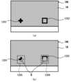
次に、インプリント結果の異常について説明する。図5は、(工程S103の完了後、例えば、工程S104、S105において)型Mと基板S上のインプリント材IMとが接触している状態の側面図である。浸み出しとは、図5(a)に示すように、型Mとインプリント材IMとの接触領域からインプリント材IMがはみ出した状態をいう。また、未充填とは、図5(b)に示すように、型Mと基板Sとの間にインプリント材IMが充填されない部分が発生する状態をいう。Next, abnormalities in the imprint results will be described. Figure 5 is a side view of the state in which the mold M and the imprint material IM on the substrate S are in contact (after completion of step S103, for example, in steps S104 and S105). Seepage refers to a state in which the imprint material IM protrudes from the contact area between the mold M and the imprint material IM, as shown in Figure 5(a). Moreover, unfilled refers to a state in which there are portions between the mold M and the substrate S that are not filled with the imprint material IM, as shown in Figure 5(b).
図6には、浸み出しおよび未充填が発生した場合に工程S108で撮像される画像の例が示されている。図6は、インプリント処理によりショット領域にインプリント材IMのパターンが形成された状態の画像を示している。通常は、図6(a)に示すように、ショット領域の境界601まで、インプリント材IMが充填されてパターンが形成される。一方、未充填の場合は、図6(b)に示すように、インプリント材IMがショット領域の境界601まで届かず、充填していない部分が白く(または黒く)撮像される。また、浸み出しの場合、図6(c)に示すように、インプリント材IMがショット領域の境界601からはみ出して、境界601を越えて黒く(または白く)撮像される。Figure 6 shows an example of an image captured in step S108 when seepage and underfilling occur. Figure 6 shows an image of a state in which a pattern of imprint material IM has been formed in the shot area by the imprint process. Normally, as shown in Figure 6(a), the imprint material IM is filled up to the
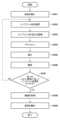
次に、図7のフローチャートを参照して、評価装置407によって実行される画像の評価方法を説明する。評価方法は、工程S108で取得した画像に含まれる異常(パターンの形成不良)を検出し、その異常の種類(浸み出し/未充填)の判定を行う。図7のフローチャートに対応する評価方法のプログラムは、例えば、記憶装置4074に記憶されおり、RAM4072にロードされた後、制御部4071(処理部)によって実行される。Next, the image evaluation method executed by the
工程S201では、制御部4071は、画像における1つ以上の異常の特徴を出力する検査用の推論モデル(学習モデル、以下では単に「モデル」ともいう。)の読み込みを行う。推論モデルは、検査対象のマテリアル(インプリント材)の条件、および、S108で取得した画像の計測条件と同一または類似の条件で取得した画像により事前に作成されたモデルである。推論モデルの作成手順については後述する。工程S202では、制御部4071は、工程S108で取得した画像を読み込む。In step S201, the
工程S203では、制御部4071は、工程S202で取得された画像を工程S201で取得された推論モデルに入力として与え、出力として画像上の1つ以上の異常の特徴を得る。異常の特徴は、画像上にあるそれぞれの異常毎に得られる。得られる異常の特徴は、異常の画像における位置、異常の種類、異常を囲む矩形の頂点の座標、検出した異常の確信度等のうちの少なくともいずれかを含みうる。ここで、検出した異常の確信度とは、異常の検出の確からしさおよび/または信頼度を表す値であり、検出した異常毎にモデルによって自動的に算出される。検出できる異常の種類は、ショット領域からはみ出して硬化した浸み出しと、ショット領域でインプリント材が充填され切っていない領域である未充填とを含みうる。その他の異常に関しても、モデルに学習させることで検出することが可能である。In step S203, the
工程S204では、制御部4071は、工程S203で入力として与えた画像上のデバイス情報(パターン情報)を読み込む。デバイス情報は、画像における検査対象のショット領域と隣接するショット領域との境界位置、ショット領域におけるデバイス領域と非デバイス領域との境界位置等の情報を含みうる。これらは、入力画像を撮像したときのショット領域の中心を原点とする座標、インプリント工程において用いた型の設計情報から求めることができる。In step S204, the
工程S205では、制御部4071は、工程S203で得たモデルから出力された異常の特徴に基づいて、該異常の種類の判定(異常の分類)を行う。工程S203では画像情報のみを用いた異常の種類が検出されるが、工程S205では、異常が存在する位置やサイズなどによって総合的にみて異常か正常かが判定される。また、工程S205では、画像上では異常の見た目が同じであっても、基板S上での異常の位置によって異常の扱いが異なる。このため、工程S205では、S203で検出された異常に対して更なる分類が行われる。この際、工程S204で読み込んだ情報を用いてもよい。工程S205では、異常のサイズによる分類や、工程S204で読み込んだパターン情報と異常の位置を用いて分類が行われる。In step S205, the
以下では、工程S205で行われる異常の分類の方法について説明する。The method for classifying anomalies performed in step S205 is described below.
まず、図10を参照して、浸み出しの分類の例を説明する。分類(判定)は、ショット領域の境界と異常の位置およびサイズとの関係に基づいて行われうる。図10(a),(b),(c)にはそれぞれ、ショット領域の画像IMGの例が示されている。各画像のグレーで示された領域はインプリント材IMが充填された領域である。領域Dは、工程S203においてモデルが異常として出力した浸み出し領域である。浸み出しの領域Dはさまざまである。黒い点のように現れる場合もあれば、画像の計測条件やマテリアルの特性によって違った見え方で現れる場合もある。ショット境界1001は、検査対象のショット領域とそれに隣接するショット領域との境界であり、その位置は工程S204で読み込んだ情報から定義される。これらの情報から異常のカテゴリをさらにカテゴリ分けすることができる。図10(a)の場合は、浸み出しの領域Dは、検査対象のショット領域側に存在し、ショット境界1001を越えていない。この場合の浸み出しは、小さい浸み出しとして分類できる。図10(b)の場合は、浸み出しの領域Dは、検査対象のショット領域に隣接するショット領域側に存在している。この浸み出しは、隣接ショット領域からの浸み出しであるから、検出対象外の異常として分類できる。図10(c)の場合は、浸み出しの領域Dは検査対象のショット領域側に存在し、かつショット境界1001を越えるものである。このような浸み出しは、大きい浸み出しとして分類できる。First, referring to FIG. 10, an example of classification of seepage will be described. Classification (determination) can be performed based on the relationship between the shot area boundary and the position and size of the anomaly. FIGS. 10(a), (b), and (c) show examples of shot area images IMG. The gray areas in each image are areas filled with the imprint material IM. Area D is a seepage area output by the model as an anomaly in step S203. The seepage area D can vary. It may appear as a black dot, or it may appear differently depending on the measurement conditions of the image and the characteristics of the material. The
次に、図10で示した判定を行うための方法について説明する。判定時にはモデルが検出した異常の位置、サイズ、種類、ショット境界の位置を用いる。制御部4071は、モデルが出力した異常の領域Dにおける座標を得て、これを異常の位置やサイズとして用いる。また、異常の種類もモデルの出力として得られてもよい。ショット境界1001の情報は事前定義された値から得ることもできるし、型の設計情報から計算して得てもよい。ショット境界1001の情報は、画像における境界となる位置のピクセルの座標群で表現されうる。図10の場合、ショット境界1001の線上のピクセル群の座標および領域Dにおける座標を、異常(浸み出し)の位置およびサイズを判定する情報として用いる。Next, a method for making the judgment shown in FIG. 10 will be described. When making the judgment, the position, size, and type of the abnormality detected by the model, and the position of the shot boundary are used. The
図10(a)では、モデルが出力した異常の領域Dにおける座標の全てが、ショット境界1001の座標を越えない、すなわち、検査対象のショット領域内の座標であるため、小さい異常であると判別する。図10(b)では、モデルが出力した異常の領域Dにおける座標の全てが、ショット境界1001の座標を越える、すなわち、隣接ショット領域に含まれる座標であるため、隣接ショット領域における異常であると判別する。図10(c)では、モデルが出力した異常の領域Dにおける座標の一部が、ショット境界1001の座標を越える、すなわち、領域Dの一部が隣接ショット領域に含まれるため、大きい浸み出しと判定できる。このとき、浸み出しのサイズに対して事前に閾値を設定しておき、領域Dにおける座標から算出された縦方向または横方向の長さから異常の分類をすることもできる。In FIG. 10(a), all of the coordinates in the abnormal region D output by the model do not exceed the coordinates of the
図11を参照して、未充填の分類の例を説明する。分類(判定)は、ショット領域におけるデバイス領域と非デバイス領域との境界を示すデバイス境界と異常の位置およびサイズとの関係に基づいて行われうる。図11(a)および(b)にはそれぞれ、ショット領域の画像IMGが示されている。各画像のグレーで示された領域はインプリント材IMが充填された領域である。白い領域Nは、工程S203においてモデルが異常として出力した未充填の領域である。デバイス境界1101は、ショット領域におけるデバイス領域と非デバイス領域との境界である。デバイス境界1101は画像情報のみからは判断できないため、工程S204で読み込んだ情報から定義される。これらの情報から異常のカテゴリをさらにカテゴリ分けすることができる。図11(a)の場合は、未充填の領域Nはデバイス境界1101を越えた非デバイス領域にあるため、領域Nは非デバイス領域の未充填と分類できる。また、図11(b)の場合は、未充填の領域Nはデバイス境界110を越えずデバイス領域内に存在するため、領域Nはデバイス領域内の未充填と分類できる。上記に挙げた分類の基準やカテゴリは一例であり、他の設計情報や条件と組み合わせて異なる分類をすることもできる。An example of classification of unfilled areas will be described with reference to FIG. 11. Classification (determination) can be performed based on the relationship between the device boundary, which indicates the boundary between the device area and the non-device area in the shot area, and the position and size of the anomaly. In each of FIGS. 11(a) and (b), an image IMG of the shot area is shown. The areas shown in gray in each image are areas filled with the imprint material IM. The white area N is an unfilled area output by the model as an anomaly in step S203. The device boundary 1101 is the boundary between the device area and the non-device area in the shot area. Since the device boundary 1101 cannot be determined from image information alone, it is defined from the information read in step S204. The categories of anomalies can be further categorized from these pieces of information. In the case of FIG. 11(a), the unfilled area N is in the non-device area beyond the device boundary 1101, so the area N can be classified as unfilled in the non-device area. In the case of FIG. 11(b), the unfilled area N does not cross the
次に、図11で示した判定を行うための方法について説明する。判定時にはモデルが検出した異常の位置、サイズ、種類、ショット境界、デバイス境界の位置を用いる。制御部4071は、モデルが出力した異常の領域Nにおける座標を得て、これを異常の位置やサイズとして用いる。また、異常の種類もモデルの出力として得られる。デバイス境界1101の情報は事前定義された値から得ることもできるし、型の設計情報から計算して得てもよい。デバイス境界1101の情報は、画像における境界となる位置のピクセルの座標群で表現される。図11の場合、デバイス境界1101の線上のピクセル群の座標および領域Nにおける座標を、異常(未充填)の位置およびサイズを判定する情報として用いる。Next, the method for making the judgment shown in FIG. 11 will be described. When making the judgment, the position, size, type, shot boundary, and device boundary positions of the abnormality detected by the model are used. The
図11(a)では、モデルが出力した異常の領域Nにおける座標の全てが、デバイス境界1101の座標を越える、すなわち、非デバイス領域側にあるため、デバイス領域外の未充填であると判別する。図11(b)では、モデルが出力した異常の領域Nにおける座標の全てが、デバイス境界1101の座標を越えない、すなわち、デバイス領域側にあるため、デバイス領域上の未充填と分類できる。In FIG. 11(a), all of the coordinates in the abnormal area N output by the model exceed the coordinates of the device boundary 1101, i.e., they are on the non-device area side, so they are determined to be unfilled outside the device area. In FIG. 11(b), all of the coordinates in the abnormal area N output by the model do not exceed the coordinates of the device boundary 1101, i.e., they are on the device area side, so they can be classified as unfilled on the device area.
図12を参照して、マークで発生した未充填の分類の例を説明する。分類(判定)は、ショット領域に含まれるマークの位置と異常の位置およびサイズとの関係に基づいて行われうる。図12(a),(b)にはそれぞれ、ショット領域の画像IMGが示されている。各画像のグレーで示された領域はインプリント材IMが充填された領域である。ショット領域には、互いに形状の異なる第1マーク1201と第2マーク1202とが含まれている。図12(a)において、第1マーク1201と第2マーク1202は黒色で表されており、インプリント材IMがマークの内側に充填した正常な状態である。一方、図12(b)において、第1マーク1201と1202は、一部が白色で表されており、インプリント材IMが十分にマークの内側に充填していない状態である(未充填)。白色で表された領域が、工程S203においてモデルが異常として出力する未充填Nである。With reference to FIG. 12, an example of classification of unfilled marks will be described. Classification (determination) can be performed based on the relationship between the position of the mark included in the shot area and the position and size of the abnormality. Each of FIGS. 12(a) and (b) shows an image IMG of a shot area. The areas shown in gray in each image are areas filled with the imprint material IM. The shot area includes a
図12(b)において、1205と1206は、S104で読み込んだ画像上のパターン情報の一つである、マーク毎の設計情報を示している。マーク毎の設計情報1205、1206にはそれぞれ、マークの位置と種類の情報が含まれる。工程S205では、工程S203で得られた未充填Nの有無の情報と、工程S204で得られたマークの位置および種類の情報とを組み合わせることで、未充填Nがどの種類のマークで発生しているかを分類することができる。上記に挙げた分類条件やカテゴリは一例であり、検査対象のマテリアルや設計情報、撮像時の調光条件や撮像時のモード等の装置データ等の条件によって変更することができる。In FIG. 12(b), 1205 and 1206 indicate design information for each mark, which is one of the pieces of pattern information on the image read in S104. Each of the design information for each
次に、図12で示した判定を行うための方法について説明する。判定時にはモデルが検出した異常の位置、サイズ、種類、画像上のマークの位置が用いられる。制御部4071は、モデルが出力した異常の領域Nにおける座標を得て、これを異常の位置やサイズとして用いる。また、異常の種類もモデルの出力として得られる。画像上に存在するマークの種類と位置の情報は事前定義された値から得ることもできるし、型の設計情報から計算して得てもよい。設計情報1205および1206は、実際には領域Nにおける座標とマークの種類の組み合わせで表現される。図12の場合、第1マーク1203および第2マーク1202における未充填をモデルが検出すると、未充填個所を囲む領域の座標が得られる。ここで得られた座標とマークの領域の座標とを比較することで、検出した異常がマークの領域内に存在するかを判別することができる。Next, the method for making the judgment shown in FIG. 12 will be described. The position, size, and type of the abnormality detected by the model, and the position of the mark on the image are used during the judgment. The
また、検出した各種異常に対して、確信度と所定の閾値との比較に基づいて、異常を分類することもできる。例えば、確信度が0から1の間の値で表現されるとき、検出した異常の確信度が所定の閾値(例えば、閾値=0.5)より低い場合には、該異常を最終判定の対象から除外してもよい。確信度に基づいた分類する際の、閾値等の分類条件は、検査対象のマテリアルや設計情報、撮像時の調光条件や撮像時のモード等の装置データ等の条件によって変更することができる。It is also possible to classify various detected anomalies based on a comparison between the certainty level and a predetermined threshold. For example, when the certainty level is expressed as a value between 0 and 1, if the certainty level of a detected anomaly is lower than a predetermined threshold level (e.g., threshold level = 0.5), the anomaly may be excluded from the final judgment. The classification conditions, such as the threshold level, when classifying based on the certainty level can be changed depending on conditions such as the material and design information of the inspection target, and device data such as the dimming conditions and mode at the time of imaging.
説明を図7のフローチャートに戻す。工程S206では、制御部4071は、画像上の全ての異常に対して分類を行ったかどうかを判定する。画像上の全ての異常に対して分類が完了していない場合、処理は工程S205に戻り、次の異常に対して分類を行う。画像上の全ての異常に対して分類が完了したら、処理は工程S207に進む。Returning to the explanation of the flowchart in FIG. 7, in step S206, the
工程S207では、制御部4071は、画像に対する最終判定を行う。例えば、制御装置4701は、検査対象のマテリアルの条件、目的、および、工程S205での画像中の各異常の分類結果に基づいて、画像が正常か異常かを示す最終判定値を決定する。例えば、大きな異常を含む場合に異常な画像であるとの最終判定を下す場合において、図10(a)、(b)の画像は、異常の領域Dがショット領域側からショット境界1001を越えて(跨って)存在していないため正常と最終判定される。また、図10(c)の画像は、異常の領域Dがショット領域側からショット境界1001を越えて(跨って)存在しているため異常と最終判定されうる。このとき、異常な領域の大きさの区別は、画像における異常領域の画素数の大きさで区別する方法がありうる。あるいは、デバイス領域上に未充填が存在する場合に異常と最終判定を下す場合において、デバイス領域の位置と異常の位置とを比較することにより異常の最終判定が行われうる。この場合、例えば、図11(a)の画像は、デバイス領域内に異常の領域Nが存在しないため正常な画像と最終判定される。また、図11(b)の画像は、デバイス領域内に異常の領域Nが存在するため異常な画像であると最終判定される。画像上に複数の異常がある場合には、事前に設定された条件に基づいて単一の異常を基準にして正常/異常を分類してもよい。あるいは、画像上に複数の異常がある場合には、異常の種類ごとに画像に対する判定を決定してもよい。画像に対する最終判定値を決定する際に、画像中に存在する各種異常の高さ、種類、確信度等に基づいて最終判定値を決定してもよい。各種分類結果に基づいた判定の基準は上記の例に限らない。In step S207, the
次に、ユーザが設定できる判定時のパラメータについて説明する。ユーザは異常判定時のパラメータとして、例えば、異常と判定する浸み出しのサイズや信頼度の閾値を設定することができる。図13は、表示装置4076に表示される、ユーザインタフェース(UI)画面DISP(設定部)の例である。画面上部には、検査対象の画像IMGおよびその画像に対する判定結果1303が表示されている。ユーザは、ユーザインタフェースである入力装置4075を介して、送りボタンBTNを押す、タップする等の操作を行うことで、検査対象の画像を切り替えることができる。検査対象の画像が存在しない場合にはこれらは表示されない。Next, the parameters for judgment that can be set by the user will be described. As parameters for abnormality judgment, the user can set, for example, the size of seepage that is judged to be abnormal and the reliability threshold. Figure 13 is an example of a user interface (UI) screen DISP (settings section) displayed on the
ユーザは、入力装置4075を用いて、テキストボックス1302へ値を入力することにより、あるいは、スライダ1301を動かすことにより、異常と判定する浸み出しのサイズの値を設定することができる。また、ユーザは、入力装置4075を用いて、テキストボックス1304へ値を入力することにより、あるいは、スライダ1305を動かすことにより、異常と判定する確信度に対する所定の閾値を設定することができる。このとき、スライダ1301および1305の位置とテキストボックス1302および1304に表示される値は連動して変化しうる。判定結果1303が表示されている場合、ユーザがこれらのパラメータのいずれかを変更すると判定結果1303は変更後のパラメータに応じて変化しうる。このように、本実施形態によれば、ユーザインタフェースとなる設定部および表示部が設けられ、設定部にはユーザが所望する値を入力することができ、表示部には画像および最終判定の結果が表示される。よって、ユーザは判定結果を確認しながらパラメータを設定することが可能である。ユーザは、異常検査を行う前にこのUIを用いてこれらのパラメータを事前に設定することができる。ユーザは、適用ボタン1306を押下またはタップすることによって、検査対象の画像データに対して現在設定されているパラメータを適用することができる。The user can set the value of the seepage size to be determined as an abnormality by inputting a value into the
次に、図8および図9を参照して、評価装置407より、異常検出のための推論モデル(学習モデル)を算出(学習)する方法について説明する。図8は学習時および検査時に実行される方法の模式図、図9は異常検出の学習のフローチャートである。評価装置407は、推論モデルを機械学習によって生成する機械学習部を備えうる。機械学習部は、成形処理によって基板の上に形成された組成物を含む画像を推論モデルの入力とし、予め得られた複数の画像と該複数の画像それぞれの異常の特徴情報との関係を教師データとして機械学習を行う。以下、具体的に説明する。Next, a method for calculating (learning) an inference model (learning model) for anomaly detection by the
工程S301で、制御部4071は、工程S108と同様に学習用の画像801を(例えば撮像により)取得する。具体的には、制御部4071は、検査時の画像を撮像する際に使用するマテリアルの条件および計測条件に基づいて、検査時の画像と類似の画像801を収集する。また、制御部4071は、複数の基板を用いて、その中の複数のショット領域で学習用の画像801を収集する。学習に用いる画像は多い方が望ましく、検出対象の異常のサンプルが十分な量含まれているものとする。In step S301, the
工程S302では、工程S301で取得した各画像に対応する異常の特徴情報の作成が行われる。具体的には、取得した各画像を目視で検査の上、各画像に存在するすべての異常に対して、異常のカテゴリやサイズ、位置などの情報を含む特徴情報802が作成される。In step S302, feature information of anomalies corresponding to each image acquired in step S301 is created. Specifically, each acquired image is visually inspected, and feature
工程S303では、制御部4071は、工程S301で取得した画像と工程S302で作成した異常の特徴情報に基づいて、モデルの学習を行う。事前に作成したニューラルネットワークの入力データとして画像801を用い、出力(教師)として異常の特徴情報802を用いることで最適化を行う。これらにより、学習モデル(ニューラルネットワーク)803が作成される。In step S303, the
工程S404で、制御部4071は、作成した学習モデル803を記憶部804に保存する。In step S404, the
以上説明した実施形態によれば、ショット領域における異常検出を自動化することができ、かつ、より細かく異常の分類を行うことができる。According to the embodiment described above, it is possible to automate the detection of anomalies in shot areas and classify the anomalies in more detail.
<物品製造方法の実施形態>
本発明の実施形態に係る物品製造方法は、例えば、半導体デバイス等のマイクロデバイスや微細構造を有する素子等の物品を製造するのに好適である。本実施形態の物品製造方法は、成形システムにおける成形装置により基板の上に組成物のレイヤーを形成する工程と、該レイヤーが形成された基板を処理する工程とを含みうる。更に、かかる製造方法は、他の周知の工程(酸化、成膜、蒸着、ドーピング、平坦化、エッチング、レジスト剥離、ダイシング、ボンディング、パッケージング等)を含む。本実施形態の物品製造方法は、従来の方法に比べて、物品の性能・品質・生産性・生産コストの少なくとも1つにおいて有利である。 <Embodiment of an article manufacturing method>
The article manufacturing method according to the embodiment of the present invention is suitable for manufacturing articles such as microdevices such as semiconductor devices and elements having a microstructure. The article manufacturing method of the present embodiment may include a step of forming a layer of a composition on a substrate by a molding device in a molding system, and a step of processing the substrate on which the layer is formed. Furthermore, such a manufacturing method may include other well-known steps (oxidation, film formation, deposition, doping, planarization, etching, resist stripping, dicing, bonding, packaging, etc.). The article manufacturing method of the present embodiment is advantageous in at least one of the performance, quality, productivity, and production cost of the article compared to conventional methods.
インプリント装置を用いて形成した硬化物のパターンは、各種物品の少なくとも一部に恒久的に、或いは各種物品を製造する際に一時的に、用いられる。物品とは、電気回路素子、光学素子、MEMS、記録素子、センサ、或いは、型等である。電気回路素子としては、DRAM、SRAM、フラッシュメモリ、MRAMのような、揮発性或いは不揮発性の半導体メモリや、LSI、CCD、イメージセンサ、FPGAのような半導体素子等が挙げられる。型としては、インプリント用のモールド等が挙げられる。The pattern of the cured material formed using the imprinting device is used permanently as at least a part of various articles, or temporarily when manufacturing various articles. The articles include electric circuit elements, optical elements, MEMS, recording elements, sensors, and molds. Examples of electric circuit elements include volatile or non-volatile semiconductor memories such as DRAM, SRAM, flash memory, and MRAM, and semiconductor elements such as LSI, CCD, image sensors, and FPGAs. Examples of molds include molds for imprinting.
硬化物のパターンは、上記物品の少なくとも一部の構成部材として、そのまま用いられるか、或いは、レジストマスクとして一時的に用いられる。基板の加工工程においてエッチング又はイオン注入等が行われた後、レジストマスクは除去される。The pattern of the cured material is used as it is, as at least a part of the component of the article, or is used temporarily as a resist mask. After etching or ion implantation is performed in the substrate processing step, the resist mask is removed.
次に、物品製造方法について説明する。図15の工程SAでは、絶縁体等の被加工材2zが表面に形成されたシリコン基板等の基板1zを用意し、続いて、インクジェット法等により、被加工材2zの表面にインプリント材3zを付与する。ここでは、複数の液滴状になったインプリント材3zが基板上に付与された様子を示している。Next, a method for manufacturing an article will be described. In step SA of FIG. 15, a
図15の工程SBでは、インプリント用の型4zを、その凹凸パターンが形成された側を基板上のインプリント材3zに向け、対向させる。図15の工程SCでは、インプリント材3zが付与された基板1zと型4zとを接触させ、圧力を加える。インプリント材3zは型4zと被加工材2zとの隙間に充填される。この状態で硬化用のエネルギーとして光を型4zを介して照射すると、インプリント材3zは硬化する。In step SB of FIG. 15, the
図15の工程SDでは、インプリント材3zを硬化させた後、型4zと基板1zを引き離すと、基板1z上にインプリント材3zの硬化物のパターンが形成される。この硬化物のパターンは、型の凹部が硬化物の凸部に、型の凸部が硬化物の凹部に対応した形状になっており、即ち、インプリント材3zに型4zの凹凸パターンが転写されたことになる。In process SD of FIG. 15, after the
図15の工程SEでは、硬化物のパターンを耐エッチングマスクとしてエッチングを行うと、被加工材2zの表面のうち、硬化物が無いか或いは薄く残存した部分が除去され、溝5zとなる。図15の工程SFでは、硬化物のパターンを除去すると、被加工材2zの表面に溝5zが形成された物品を得ることができる。ここでは硬化物のパターンを除去したが、加工後も除去せずに、例えば、半導体素子等に含まれる層間絶縁用の膜、つまり、物品の構成部材として利用してもよい。In step SE of FIG. 15, etching is performed using the pattern of the cured material as an etching-resistant mask, and the portions of the surface of the
(他の実施形態)
本発明は、上述の実施形態の1以上の機能を実現するプログラムを、ネットワーク又は記憶媒体を介してシステム又は装置に供給し、そのシステム又は装置のコンピュータにおける1つ以上のプロセッサがプログラムを読み出し実行する処理でも実現可能である。また、1以上の機能を実現する回路(例えば、ASIC)によっても実現可能である。 Other Embodiments
The present invention can also be realized by a process in which a program for implementing one or more of the functions of the above-described embodiments is supplied to a system or device via a network or a storage medium, and one or more processors in a computer of the system or device read and execute the program. The present invention can also be realized by a circuit (e.g., ASIC) for implementing one or more of the functions.
発明は上記実施形態に制限されるものではなく、発明の精神及び範囲から離脱することなく、様々な変更及び変形が可能である。従って、発明の範囲を公にするために請求項を添付する。The invention is not limited to the above-described embodiment, and various modifications and variations are possible without departing from the spirit and scope of the invention. Therefore, the following claims are appended to disclose the scope of the invention.
IMP:インプリント装置、S:基板、M:型、110:制御部、102:基板保持部、105:基板駆動機構、121:型保持部、122:型駆動機構、407:評価装置IMP: Imprint device, S: Substrate, M: Mold, 110: Control unit, 102: Substrate holder, 105: Substrate drive mechanism, 121: Mold holder, 122: Mold drive mechanism, 407: Evaluation device
Claims (17)
Translated fromJapanese前記成形処理によって前記基板の上に形成された前記組成物を含む画像を取得する取得部と、
前記取得された画像を前記評価のために処理する処理部と、を有し、
前記処理部は、
前記取得された画像における異常の位置とサイズを推論モデルに従い出力し、
前記ショット領域におけるデバイス領域と非デバイス領域との境界と、前記異常の前記位置および前記サイズとの関係に基づいて、前記異常の種類の判定を行い、
前記判定の結果に基づいて、前記画像が正常な画像であるか異常を含む画像であるかの最終判定を行う、
ことを特徴とする評価装置。 An evaluation device for evaluating a composition formed on a substrate by a molding process, the molding process being a process for forming the composition on the substrate, the composition being a cured product of the moldable material, by curing the moldable material ona shot region of the substrate while the mold is in contact with the mold, the evaluation device comprising:
an acquisition unit that acquires an image including the composition formed on the substrate by the molding process;
a processing unit for processing the acquired image for the evaluation;
The processing unit includes:
outputtingthe location and size of the anomaly in the acquired image according to an inference model;
determining a type ofthe abnormality based ona relationship between a boundary between a device area and a non-device area in the shot area and the position and the size of the abnormality ;
and making a final determination as to whether the image is a normal image or an image including an abnormality based on the result of the determination.
An evaluation device comprising:
前記判定は、前記ショット領域の境界と前記異常の前記位置および前記サイズとの関係に基づいて行われる、
ことを特徴とする請求項5に記載の評価装置。 the molding process is an imprint process in which an imprint material, which is the moldable material supplied onto a shot area on a substrate where a pattern is to be formed, is brought into contact with a pattern portion of the mold, thereby transferring a pattern of the mold to the imprint material;
the determination is made based on a relationship between a boundary of the shot area and the position and the size of the anomaly.
6. The evaluation device according to claim 5.
前記判定は、前記ショット領域に含まれるマークの位置と、前記異常の前記位置および前記サイズとの関係に基づいて行われる、
ことを特徴とする請求項5に記載の評価装置。 the molding process is an imprint process in which an imprint material, which is the moldable material supplied onto a shot area on a substrate where a pattern is to be formed, is brought into contact with a pattern portion of the mold, thereby transferring a pattern of the mold to the imprint material;
the determination is made based on a relationship between a position of a mark included in the shot areaand the position and size of the abnormality.
6. The evaluation device according to claim 5.
前記異常のうち前記はみ出しと判定された異常の部分が前記ショット領域の境界を越えて存在している場合、前記最終判定は、前記画像を異常を含む画像であると判定する、
ことを特徴とする請求項6に記載の評価装置。 the type of abnormality includes overflow of the imprint material;
When the portion of theabnormality determined to be the protrusion is present beyond the boundary of the shot area, the final determination is made to determine that the image is an image including an abnormality.
7. The evaluation device according to claim 6.
前記異常のうち前記未充填と判定された異常が前記デバイス領域内に存在している場合、前記最終判定は、前記画像を異常を含む画像であると判定する、
ことを特徴とする請求項1に記載の評価装置。 the type of abnormality includes an underfill ofthe moldable material ;
When theanomaly determined to be the non-filling among the anomalies exists within the device region, the final determination is made by determining that the image is an image including an anomaly.
2. The evaluation device according to claim1 .
前記成形処理によって前記基板の上に形成された前記組成物を含む画像を取得する取得部と、an acquisition unit that acquires an image including the composition formed on the substrate by the molding process;
前記取得された画像を前記評価のために処理する処理部と、を有し、a processing unit for processing the acquired image for the evaluation;
前記処理部は、The processing unit includes:
前記取得された画像における異常の位置とサイズを推論モデルに従い出力し、outputting the location and size of the anomaly in the acquired image according to an inference model;
前記ショット領域に含まれるマークの位置と、前記異常の前記位置および前記サイズとの関係に基づいて、前記異常の種類の判定を行い、determining a type of the abnormality based on a relationship between a position of a mark included in the shot area and the position and size of the abnormality;
前記判定の結果に基づいて、前記画像が正常な画像であるか異常を含む画像であるかの最終判定を行う、and making a final determination as to whether the image is a normal image or an image including an abnormality based on the result of the determination.
ことを特徴とする評価装置。An evaluation device comprising:
前記成形処理によって前記基板の上に形成された前記組成物を含む画像を取得する工程と、
前記取得された画像における異常の位置とサイズを推論モデルに従い出力する工程と、
前記ショット領域におけるデバイス領域と非デバイス領域との境界と、前記異常の前記位置および前記サイズとの関係に基づいて、前記異常の種類の判定を行う工程と、
前記判定の結果に基づいて、前記画像が正常な画像であるか異常を含む画像であるかの最終判定を行う工程と、
を有することを特徴とする評価方法。 A method for evaluating a composition formed on a substrate by a molding process, the molding process being a process for forming the composition on the substrate, the composition being a cured product of the moldable material, by curing the moldable material ona shot region of the substrate while the mold is in contact with the mold, the method comprising:
obtaining an image including the composition formed on the substrate by the molding process;
outputtinga location and a size of the anomaly in the acquired image according to an inference model;
determining a type ofthe abnormality based ona relationship between a boundary between a device area and a non-device area in the shot area and the position and size of the abnormality ;
making a final judgment as to whether the image is a normal image or an image including an abnormality based on a result of the judgment;
The evaluation method according to claim 1,
請求項1から13のいずれか1項に記載の評価装置と、
を含む、ことを特徴とする成形システム。 a molding apparatus for performing a molding process in which a moldable material on a substrate is contacted with a mold and the moldable material is cured to form a composition on the substrate, the composition comprising a cured product of the moldable material;
An evaluation device according to any one of claims 1 to 13;
A molding system comprising:
前記レイヤーが形成された前記基板を処理する工程と、
を有し、前記処理された前記基板から物品を製造する、ことを特徴とする物品製造方法。 forming a layer of the composition on a substrate with the molding device of claim 16;
treating the substrate on which the layer is formed;
and manufacturing an article from the processed substrate.
Priority Applications (3)
| Application Number | Priority Date | Filing Date | Title |
|---|---|---|---|
| JP2021055838AJP7657631B2 (en) | 2021-03-29 | 2021-03-29 | EVALUATION APPARATUS, PROGRAM, EVALUATION METHOD, MOLDING SYSTEM, AND ARTICLE MANUFACTURING METHOD |
| US17/703,460US12293505B2 (en) | 2021-03-29 | 2022-03-24 | Evaluation apparatus, computer-readable storage medium, evaluation method, forming system, and article manufacturing method |
| KR1020220038555AKR102856576B1 (en) | 2021-03-29 | 2022-03-29 | Evaluation apparatus, program, evaluation method, forming system, and article manufacturing method |
Applications Claiming Priority (1)
| Application Number | Priority Date | Filing Date | Title |
|---|---|---|---|
| JP2021055838AJP7657631B2 (en) | 2021-03-29 | 2021-03-29 | EVALUATION APPARATUS, PROGRAM, EVALUATION METHOD, MOLDING SYSTEM, AND ARTICLE MANUFACTURING METHOD |
Publications (2)
| Publication Number | Publication Date |
|---|---|
| JP2022152899A JP2022152899A (en) | 2022-10-12 |
| JP7657631B2true JP7657631B2 (en) | 2025-04-07 |
Family
ID=83364730
Family Applications (1)
| Application Number | Title | Priority Date | Filing Date |
|---|---|---|---|
| JP2021055838AActiveJP7657631B2 (en) | 2021-03-29 | 2021-03-29 | EVALUATION APPARATUS, PROGRAM, EVALUATION METHOD, MOLDING SYSTEM, AND ARTICLE MANUFACTURING METHOD |
Country Status (3)
| Country | Link |
|---|---|
| US (1) | US12293505B2 (en) |
| JP (1) | JP7657631B2 (en) |
| KR (1) | KR102856576B1 (en) |
Families Citing this family (1)
| Publication number | Priority date | Publication date | Assignee | Title |
|---|---|---|---|---|
| JP6896036B2 (en)* | 2019-09-30 | 2021-06-30 | キヤノン株式会社 | Information processing equipment, judgment method, imprint equipment, lithography system, article manufacturing method and program |
Citations (4)
| Publication number | Priority date | Publication date | Assignee | Title |
|---|---|---|---|---|
| JP2019080047A (en) | 2017-10-23 | 2019-05-23 | キヤノン株式会社 | Imprint device and article manufacturing method |
| WO2020095909A1 (en) | 2018-11-07 | 2020-05-14 | 株式会社 東芝 | Image processing device, image processing method, and program |
| JP2020145383A (en) | 2019-03-08 | 2020-09-10 | キヤノン株式会社 | Control method of imprint device, imprint device, and goods manufacturing method |
| JP2021027349A (en) | 2019-08-08 | 2021-02-22 | キヤノン株式会社 | System and method for classifying images of imprint film |
Family Cites Families (10)
| Publication number | Priority date | Publication date | Assignee | Title |
|---|---|---|---|---|
| US8349241B2 (en)* | 2002-10-04 | 2013-01-08 | Molecular Imprints, Inc. | Method to arrange features on a substrate to replicate features having minimal dimensional variability |
| US20120261849A1 (en)* | 2011-04-14 | 2012-10-18 | Canon Kabushiki Kaisha | Imprint apparatus, and article manufacturing method using same |
| JP6315963B2 (en)* | 2013-12-09 | 2018-04-25 | キヤノン株式会社 | Imprint apparatus and article manufacturing method |
| JP6706983B2 (en)* | 2016-07-12 | 2020-06-10 | キヤノン株式会社 | Imprint apparatus and method of manufacturing article |
| US11580398B2 (en) | 2016-10-14 | 2023-02-14 | KLA-Tenor Corp. | Diagnostic systems and methods for deep learning models configured for semiconductor applications |
| US11681216B2 (en)* | 2017-08-25 | 2023-06-20 | Canon Kabushiki Kaisha | Imprint apparatus, imprint method, article manufacturing method, molding apparatus, and molding method |
| JP6498343B2 (en)* | 2017-08-25 | 2019-04-10 | キヤノン株式会社 | Imprint apparatus, imprint method, article manufacturing method, molding apparatus, and molding method. |
| JP7305430B2 (en)* | 2018-06-29 | 2023-07-10 | キヤノン株式会社 | Information processing apparatus, program, lithographic apparatus, lithographic system, and method of manufacturing article |
| US10901327B2 (en) | 2018-12-20 | 2021-01-26 | Canon Kabushiki Kaisha | Automatic defect analyzer for nanoimprint lithography using image analysis |
| WO2022187079A1 (en)* | 2021-03-04 | 2022-09-09 | Applied Materials, Inc. | Pixel and region classification of film non-uniformity based on processing of substrate images |
- 2021
- 2021-03-29JPJP2021055838Apatent/JP7657631B2/enactiveActive
- 2022
- 2022-03-24USUS17/703,460patent/US12293505B2/enactiveActive
- 2022-03-29KRKR1020220038555Apatent/KR102856576B1/enactiveActive
Patent Citations (4)
| Publication number | Priority date | Publication date | Assignee | Title |
|---|---|---|---|---|
| JP2019080047A (en) | 2017-10-23 | 2019-05-23 | キヤノン株式会社 | Imprint device and article manufacturing method |
| WO2020095909A1 (en) | 2018-11-07 | 2020-05-14 | 株式会社 東芝 | Image processing device, image processing method, and program |
| JP2020145383A (en) | 2019-03-08 | 2020-09-10 | キヤノン株式会社 | Control method of imprint device, imprint device, and goods manufacturing method |
| JP2021027349A (en) | 2019-08-08 | 2021-02-22 | キヤノン株式会社 | System and method for classifying images of imprint film |
Also Published As
| Publication number | Publication date |
|---|---|
| US12293505B2 (en) | 2025-05-06 |
| US20220309647A1 (en) | 2022-09-29 |
| KR102856576B1 (en) | 2025-09-09 |
| JP2022152899A (en) | 2022-10-12 |
| KR20220135207A (en) | 2022-10-06 |
Similar Documents
| Publication | Publication Date | Title |
|---|---|---|
| US11721013B2 (en) | Information processing apparatus, determination method, imprint apparatus, lithography system, article manufacturing method, and non-transitory computer-readable storage medium | |
| JP7494037B2 (en) | Information processing device, judgment method, inspection device, molding device, and article manufacturing method | |
| TWI392578B (en) | Real time imprint process diagnostics for defects | |
| TWI629709B (en) | Imprint apparatus, imprinting method, and method of manufacturing product | |
| US11061335B2 (en) | Information processing apparatus, storage medium, lithography apparatus, lithography system, and article manufacturing method | |
| JP7270417B2 (en) | IMPRINT APPARATUS CONTROL METHOD, IMPRINT APPARATUS, AND ARTICLE MANUFACTURING METHOD | |
| JP7657631B2 (en) | EVALUATION APPARATUS, PROGRAM, EVALUATION METHOD, MOLDING SYSTEM, AND ARTICLE MANUFACTURING METHOD | |
| KR102543393B1 (en) | Information processing apparatus, storage medium, lithography apparatus, lithography system, and article manufacturing method | |
| JP6971599B2 (en) | Imprint equipment, defect inspection method, pattern formation method and article manufacturing method | |
| JP2024003614A (en) | Evaluation device, information processing device, program, film forming system, and article manufacturing method | |
| JP2017069272A (en) | Imprint device, imprint method, foreign matter detecting method, and article manufacturing method | |
| JP2025058737A (en) | GENERATION METHOD, LEARNING METHOD, PROGRAM, GENERATION DEVICE, EVALUATION DEVICE, FILM FORMING SYSTEM, AND ARTICLE MANUFACTURING METHOD | |
| JP7361831B2 (en) | Information processing equipment, molding equipment, molding methods, and article manufacturing methods | |
| JP2025098815A (en) | Information processing apparatus, method for controlling information processing apparatus, imprint apparatus, and method for manufacturing article | |
| JP2022035214A (en) | Information processing equipment, inspection equipment, molding equipment, inspection methods, article manufacturing methods, programs, and learning model creation methods. | |
| JP2019192753A (en) | Molding apparatus and article manufacturing method | |
| JP2025092152A (en) | Information processing device, method, molding device, lithography system, article manufacturing method, and program | |
| US20250076213A1 (en) | Foreign substance inspection method, foreign substance inspection apparatus, molding method, molding apparatus, and article manufacturing method | |
| JP2023031137A (en) | Imprint method, imprint device, manufacturing method of article, model, generation method of model and program | |
| JP2025053638A (en) | Molding system, molding method, and method for manufacturing an article |
Legal Events
| Date | Code | Title | Description |
|---|---|---|---|
| A621 | Written request for application examination | Free format text:JAPANESE INTERMEDIATE CODE: A621 Effective date:20240325 | |
| A977 | Report on retrieval | Free format text:JAPANESE INTERMEDIATE CODE: A971007 Effective date:20241127 | |
| A131 | Notification of reasons for refusal | Free format text:JAPANESE INTERMEDIATE CODE: A131 Effective date:20241202 | |
| A521 | Request for written amendment filed | Free format text:JAPANESE INTERMEDIATE CODE: A523 Effective date:20250130 | |
| TRDD | Decision of grant or rejection written | ||
| A01 | Written decision to grant a patent or to grant a registration (utility model) | Free format text:JAPANESE INTERMEDIATE CODE: A01 Effective date:20250225 | |
| A61 | First payment of annual fees (during grant procedure) | Free format text:JAPANESE INTERMEDIATE CODE: A61 Effective date:20250326 | |
| R150 | Certificate of patent or registration of utility model | Ref document number:7657631 Country of ref document:JP Free format text:JAPANESE INTERMEDIATE CODE: R150 |