JP7655276B2 - STACKED SEMICONDUCTOR PACKAGE AND ITS MANUFACTURING METHOD - Google Patents
STACKED SEMICONDUCTOR PACKAGE AND ITS MANUFACTURING METHODDownload PDFInfo
- Publication number
- JP7655276B2 JP7655276B2JP2022090321AJP2022090321AJP7655276B2JP 7655276 B2JP7655276 B2JP 7655276B2JP 2022090321 AJP2022090321 AJP 2022090321AJP 2022090321 AJP2022090321 AJP 2022090321AJP 7655276 B2JP7655276 B2JP 7655276B2
- Authority
- JP
- Japan
- Prior art keywords
- component
- substrate
- main surface
- integrated circuit
- components
- Prior art date
- Legal status (The legal status is an assumption and is not a legal conclusion. Google has not performed a legal analysis and makes no representation as to the accuracy of the status listed.)
- Active
Links
Images


Classifications
- H—ELECTRICITY
- H01—ELECTRIC ELEMENTS
- H01L—SEMICONDUCTOR DEVICES NOT COVERED BY CLASS H10
- H01L25/00—Assemblies consisting of a plurality of semiconductor or other solid state devices
- H01L25/16—Assemblies consisting of a plurality of semiconductor or other solid state devices the devices being of types provided for in two or more different subclasses of H10B, H10D, H10F, H10H, H10K or H10N, e.g. forming hybrid circuits
- H—ELECTRICITY
- H01—ELECTRIC ELEMENTS
- H01L—SEMICONDUCTOR DEVICES NOT COVERED BY CLASS H10
- H01L25/00—Assemblies consisting of a plurality of semiconductor or other solid state devices
- H01L25/03—Assemblies consisting of a plurality of semiconductor or other solid state devices all the devices being of a type provided for in a single subclass of subclasses H10B, H10D, H10F, H10H, H10K or H10N, e.g. assemblies of rectifier diodes
- H01L25/04—Assemblies consisting of a plurality of semiconductor or other solid state devices all the devices being of a type provided for in a single subclass of subclasses H10B, H10D, H10F, H10H, H10K or H10N, e.g. assemblies of rectifier diodes the devices not having separate containers
- H01L25/065—Assemblies consisting of a plurality of semiconductor or other solid state devices all the devices being of a type provided for in a single subclass of subclasses H10B, H10D, H10F, H10H, H10K or H10N, e.g. assemblies of rectifier diodes the devices not having separate containers the devices being of a type provided for in group H10D89/00
- H01L25/0657—Stacked arrangements of devices
- H—ELECTRICITY
- H01—ELECTRIC ELEMENTS
- H01L—SEMICONDUCTOR DEVICES NOT COVERED BY CLASS H10
- H01L23/00—Details of semiconductor or other solid state devices
- H01L23/58—Structural electrical arrangements for semiconductor devices not otherwise provided for, e.g. in combination with batteries
- H01L23/64—Impedance arrangements
- H01L23/645—Inductive arrangements
- H—ELECTRICITY
- H01—ELECTRIC ELEMENTS
- H01L—SEMICONDUCTOR DEVICES NOT COVERED BY CLASS H10
- H01L24/00—Arrangements for connecting or disconnecting semiconductor or solid-state bodies; Methods or apparatus related thereto
- H01L24/01—Means for bonding being attached to, or being formed on, the surface to be connected, e.g. chip-to-package, die-attach, "first-level" interconnects; Manufacturing methods related thereto
- H01L24/02—Bonding areas ; Manufacturing methods related thereto
- H01L24/07—Structure, shape, material or disposition of the bonding areas after the connecting process
- H01L24/08—Structure, shape, material or disposition of the bonding areas after the connecting process of an individual bonding area
- H—ELECTRICITY
- H01—ELECTRIC ELEMENTS
- H01L—SEMICONDUCTOR DEVICES NOT COVERED BY CLASS H10
- H01L24/00—Arrangements for connecting or disconnecting semiconductor or solid-state bodies; Methods or apparatus related thereto
- H01L24/01—Means for bonding being attached to, or being formed on, the surface to be connected, e.g. chip-to-package, die-attach, "first-level" interconnects; Manufacturing methods related thereto
- H01L24/10—Bump connectors ; Manufacturing methods related thereto
- H01L24/15—Structure, shape, material or disposition of the bump connectors after the connecting process
- H01L24/16—Structure, shape, material or disposition of the bump connectors after the connecting process of an individual bump connector
- H—ELECTRICITY
- H01—ELECTRIC ELEMENTS
- H01L—SEMICONDUCTOR DEVICES NOT COVERED BY CLASS H10
- H01L24/00—Arrangements for connecting or disconnecting semiconductor or solid-state bodies; Methods or apparatus related thereto
- H01L24/80—Methods for connecting semiconductor or other solid state bodies using means for bonding being attached to, or being formed on, the surface to be connected
- H—ELECTRICITY
- H01—ELECTRIC ELEMENTS
- H01L—SEMICONDUCTOR DEVICES NOT COVERED BY CLASS H10
- H01L25/00—Assemblies consisting of a plurality of semiconductor or other solid state devices
- H01L25/03—Assemblies consisting of a plurality of semiconductor or other solid state devices all the devices being of a type provided for in a single subclass of subclasses H10B, H10D, H10F, H10H, H10K or H10N, e.g. assemblies of rectifier diodes
- H01L25/04—Assemblies consisting of a plurality of semiconductor or other solid state devices all the devices being of a type provided for in a single subclass of subclasses H10B, H10D, H10F, H10H, H10K or H10N, e.g. assemblies of rectifier diodes the devices not having separate containers
- H01L25/065—Assemblies consisting of a plurality of semiconductor or other solid state devices all the devices being of a type provided for in a single subclass of subclasses H10B, H10D, H10F, H10H, H10K or H10N, e.g. assemblies of rectifier diodes the devices not having separate containers the devices being of a type provided for in group H10D89/00
- H01L25/0655—Assemblies consisting of a plurality of semiconductor or other solid state devices all the devices being of a type provided for in a single subclass of subclasses H10B, H10D, H10F, H10H, H10K or H10N, e.g. assemblies of rectifier diodes the devices not having separate containers the devices being of a type provided for in group H10D89/00 the devices being arranged next to each other
- H—ELECTRICITY
- H01—ELECTRIC ELEMENTS
- H01L—SEMICONDUCTOR DEVICES NOT COVERED BY CLASS H10
- H01L25/00—Assemblies consisting of a plurality of semiconductor or other solid state devices
- H01L25/18—Assemblies consisting of a plurality of semiconductor or other solid state devices the devices being of the types provided for in two or more different main groups of the same subclass of H10B, H10D, H10F, H10H, H10K or H10N
- H—ELECTRICITY
- H01—ELECTRIC ELEMENTS
- H01F—MAGNETS; INDUCTANCES; TRANSFORMERS; SELECTION OF MATERIALS FOR THEIR MAGNETIC PROPERTIES
- H01F27/00—Details of transformers or inductances, in general
- H01F27/28—Coils; Windings; Conductive connections
- H01F27/2804—Printed windings
- H—ELECTRICITY
- H01—ELECTRIC ELEMENTS
- H01F—MAGNETS; INDUCTANCES; TRANSFORMERS; SELECTION OF MATERIALS FOR THEIR MAGNETIC PROPERTIES
- H01F27/00—Details of transformers or inductances, in general
- H01F27/28—Coils; Windings; Conductive connections
- H01F27/29—Terminals; Tapping arrangements for signal inductances
- H01F27/292—Surface mounted devices
- H—ELECTRICITY
- H01—ELECTRIC ELEMENTS
- H01F—MAGNETS; INDUCTANCES; TRANSFORMERS; SELECTION OF MATERIALS FOR THEIR MAGNETIC PROPERTIES
- H01F41/00—Apparatus or processes specially adapted for manufacturing or assembling magnets, inductances or transformers; Apparatus or processes specially adapted for manufacturing materials characterised by their magnetic properties
- H01F41/02—Apparatus or processes specially adapted for manufacturing or assembling magnets, inductances or transformers; Apparatus or processes specially adapted for manufacturing materials characterised by their magnetic properties for manufacturing cores, coils, or magnets
- H01F41/04—Apparatus or processes specially adapted for manufacturing or assembling magnets, inductances or transformers; Apparatus or processes specially adapted for manufacturing materials characterised by their magnetic properties for manufacturing cores, coils, or magnets for manufacturing coils
- H01F41/041—Printed circuit coils
- H01F41/043—Printed circuit coils by thick film techniques
- H—ELECTRICITY
- H01—ELECTRIC ELEMENTS
- H01L—SEMICONDUCTOR DEVICES NOT COVERED BY CLASS H10
- H01L2224/00—Indexing scheme for arrangements for connecting or disconnecting semiconductor or solid-state bodies and methods related thereto as covered by H01L24/00
- H01L2224/01—Means for bonding being attached to, or being formed on, the surface to be connected, e.g. chip-to-package, die-attach, "first-level" interconnects; Manufacturing methods related thereto
- H01L2224/02—Bonding areas; Manufacturing methods related thereto
- H01L2224/07—Structure, shape, material or disposition of the bonding areas after the connecting process
- H01L2224/08—Structure, shape, material or disposition of the bonding areas after the connecting process of an individual bonding area
- H01L2224/081—Disposition
- H01L2224/0812—Disposition the bonding area connecting directly to another bonding area, i.e. connectorless bonding, e.g. bumpless bonding
- H01L2224/08151—Disposition the bonding area connecting directly to another bonding area, i.e. connectorless bonding, e.g. bumpless bonding the bonding area connecting between a semiconductor or solid-state body and an item not being a semiconductor or solid-state body, e.g. chip-to-substrate, chip-to-passive
- H01L2224/08221—Disposition the bonding area connecting directly to another bonding area, i.e. connectorless bonding, e.g. bumpless bonding the bonding area connecting between a semiconductor or solid-state body and an item not being a semiconductor or solid-state body, e.g. chip-to-substrate, chip-to-passive the body and the item being stacked
- H01L2224/08265—Disposition the bonding area connecting directly to another bonding area, i.e. connectorless bonding, e.g. bumpless bonding the bonding area connecting between a semiconductor or solid-state body and an item not being a semiconductor or solid-state body, e.g. chip-to-substrate, chip-to-passive the body and the item being stacked the item being a discrete passive component
- H—ELECTRICITY
- H01—ELECTRIC ELEMENTS
- H01L—SEMICONDUCTOR DEVICES NOT COVERED BY CLASS H10
- H01L2224/00—Indexing scheme for arrangements for connecting or disconnecting semiconductor or solid-state bodies and methods related thereto as covered by H01L24/00
- H01L2224/01—Means for bonding being attached to, or being formed on, the surface to be connected, e.g. chip-to-package, die-attach, "first-level" interconnects; Manufacturing methods related thereto
- H01L2224/10—Bump connectors; Manufacturing methods related thereto
- H01L2224/15—Structure, shape, material or disposition of the bump connectors after the connecting process
- H01L2224/16—Structure, shape, material or disposition of the bump connectors after the connecting process of an individual bump connector
- H01L2224/161—Disposition
- H01L2224/16151—Disposition the bump connector connecting between a semiconductor or solid-state body and an item not being a semiconductor or solid-state body, e.g. chip-to-substrate, chip-to-passive
- H01L2224/16221—Disposition the bump connector connecting between a semiconductor or solid-state body and an item not being a semiconductor or solid-state body, e.g. chip-to-substrate, chip-to-passive the body and the item being stacked
- H01L2224/16225—Disposition the bump connector connecting between a semiconductor or solid-state body and an item not being a semiconductor or solid-state body, e.g. chip-to-substrate, chip-to-passive the body and the item being stacked the item being non-metallic, e.g. insulating substrate with or without metallisation
- H—ELECTRICITY
- H01—ELECTRIC ELEMENTS
- H01L—SEMICONDUCTOR DEVICES NOT COVERED BY CLASS H10
- H01L2224/00—Indexing scheme for arrangements for connecting or disconnecting semiconductor or solid-state bodies and methods related thereto as covered by H01L24/00
- H01L2224/80—Methods for connecting semiconductor or other solid state bodies using means for bonding being attached to, or being formed on, the surface to be connected
- H01L2224/80001—Methods for connecting semiconductor or other solid state bodies using means for bonding being attached to, or being formed on, the surface to be connected by connecting a bonding area directly to another bonding area, i.e. connectorless bonding, e.g. bumpless bonding
- H01L2224/808—Bonding techniques
- H01L2224/80894—Direct bonding, i.e. joining surfaces by means of intermolecular attracting interactions at their interfaces, e.g. covalent bonds, van der Waals forces
- H—ELECTRICITY
- H01—ELECTRIC ELEMENTS
- H01L—SEMICONDUCTOR DEVICES NOT COVERED BY CLASS H10
- H01L2224/00—Indexing scheme for arrangements for connecting or disconnecting semiconductor or solid-state bodies and methods related thereto as covered by H01L24/00
- H01L2224/80—Methods for connecting semiconductor or other solid state bodies using means for bonding being attached to, or being formed on, the surface to be connected
- H01L2224/81—Methods for connecting semiconductor or other solid state bodies using means for bonding being attached to, or being formed on, the surface to be connected using a bump connector
- H—ELECTRICITY
- H01—ELECTRIC ELEMENTS
- H01L—SEMICONDUCTOR DEVICES NOT COVERED BY CLASS H10
- H01L2225/00—Details relating to assemblies covered by the group H01L25/00 but not provided for in its subgroups
- H01L2225/03—All the devices being of a type provided for in the same main group of the same subclass of class H10, e.g. assemblies of rectifier diodes
- H01L2225/04—All the devices being of a type provided for in the same main group of the same subclass of class H10, e.g. assemblies of rectifier diodes the devices not having separate containers
- H01L2225/065—All the devices being of a type provided for in the same main group of the same subclass of class H10
- H01L2225/06503—Stacked arrangements of devices
- H01L2225/06513—Bump or bump-like direct electrical connections between devices, e.g. flip-chip connection, solder bumps
- H—ELECTRICITY
- H01—ELECTRIC ELEMENTS
- H01L—SEMICONDUCTOR DEVICES NOT COVERED BY CLASS H10
- H01L23/00—Details of semiconductor or other solid state devices
- H01L23/28—Encapsulations, e.g. encapsulating layers, coatings, e.g. for protection
- H01L23/31—Encapsulations, e.g. encapsulating layers, coatings, e.g. for protection characterised by the arrangement or shape
- H01L23/3107—Encapsulations, e.g. encapsulating layers, coatings, e.g. for protection characterised by the arrangement or shape the device being completely enclosed
- H01L23/3121—Encapsulations, e.g. encapsulating layers, coatings, e.g. for protection characterised by the arrangement or shape the device being completely enclosed a substrate forming part of the encapsulation
- H01L23/3128—Encapsulations, e.g. encapsulating layers, coatings, e.g. for protection characterised by the arrangement or shape the device being completely enclosed a substrate forming part of the encapsulation the substrate having spherical bumps for external connection
- H—ELECTRICITY
- H01—ELECTRIC ELEMENTS
- H01L—SEMICONDUCTOR DEVICES NOT COVERED BY CLASS H10
- H01L2924/00—Indexing scheme for arrangements or methods for connecting or disconnecting semiconductor or solid-state bodies as covered by H01L24/00
- H01L2924/19—Details of hybrid assemblies other than the semiconductor or other solid state devices to be connected
- H01L2924/1901—Structure
- H01L2924/1904—Component type
- H01L2924/19041—Component type being a capacitor
- H—ELECTRICITY
- H01—ELECTRIC ELEMENTS
- H01L—SEMICONDUCTOR DEVICES NOT COVERED BY CLASS H10
- H01L2924/00—Indexing scheme for arrangements or methods for connecting or disconnecting semiconductor or solid-state bodies as covered by H01L24/00
- H01L2924/19—Details of hybrid assemblies other than the semiconductor or other solid state devices to be connected
- H01L2924/1901—Structure
- H01L2924/1904—Component type
- H01L2924/19042—Component type being an inductor
- H—ELECTRICITY
- H01—ELECTRIC ELEMENTS
- H01L—SEMICONDUCTOR DEVICES NOT COVERED BY CLASS H10
- H01L2924/00—Indexing scheme for arrangements or methods for connecting or disconnecting semiconductor or solid-state bodies as covered by H01L24/00
- H01L2924/19—Details of hybrid assemblies other than the semiconductor or other solid state devices to be connected
- H01L2924/191—Disposition
- H01L2924/19101—Disposition of discrete passive components
- H01L2924/19102—Disposition of discrete passive components in a stacked assembly with the semiconductor or solid state device
- H01L2924/19103—Disposition of discrete passive components in a stacked assembly with the semiconductor or solid state device interposed between the semiconductor or solid-state device and the die mounting substrate, i.e. chip-on-passive
- H—ELECTRICITY
- H01—ELECTRIC ELEMENTS
- H01L—SEMICONDUCTOR DEVICES NOT COVERED BY CLASS H10
- H01L2924/00—Indexing scheme for arrangements or methods for connecting or disconnecting semiconductor or solid-state bodies as covered by H01L24/00
- H01L2924/19—Details of hybrid assemblies other than the semiconductor or other solid state devices to be connected
- H01L2924/191—Disposition
- H01L2924/19101—Disposition of discrete passive components
- H01L2924/19102—Disposition of discrete passive components in a stacked assembly with the semiconductor or solid state device
- H01L2924/19104—Disposition of discrete passive components in a stacked assembly with the semiconductor or solid state device on the semiconductor or solid-state device, i.e. passive-on-chip
- H—ELECTRICITY
- H10—SEMICONDUCTOR DEVICES; ELECTRIC SOLID-STATE DEVICES NOT OTHERWISE PROVIDED FOR
- H10D—INORGANIC ELECTRIC SEMICONDUCTOR DEVICES
- H10D1/00—Resistors, capacitors or inductors
- H10D1/20—Inductors
Landscapes
- Engineering & Computer Science (AREA)
- Microelectronics & Electronic Packaging (AREA)
- Power Engineering (AREA)
- Computer Hardware Design (AREA)
- Physics & Mathematics (AREA)
- Condensed Matter Physics & Semiconductors (AREA)
- General Physics & Mathematics (AREA)
- Semiconductor Integrated Circuits (AREA)
Description
Translated fromJapanese本開示は、積層型半導体パッケージおよびその製造方法に関する。This disclosure relates to a stacked semiconductor package and a method for manufacturing the same.
近年、積層型半導体パッケージの小型化と高性能化に伴い、電子回路の集積化がより進んでいる。従来、積層型半導体パッケージとしては、特許第5448393号公報(特許文献1)に記載されたものがある。この積層型半導体パッケージは、第1半導体パッケージと、第1半導体パッケージに積層された第2半導体パッケージと、第1半導体パッケージと第2半導体パッケージとの間に設けられ第1半導体パッケージおよび第2半導体パッケージに接続されるコンデンサとを有する。このように、第1半導体パッケージ、第2半導体パッケージおよびコンデンサを積層することで、フットプリント(回路や部品の面積)を小さくしている。In recent years, as stacked semiconductor packages have become smaller and more powerful, electronic circuits have become more integrated. A conventional stacked semiconductor package is described in Japanese Patent No. 5448393 (Patent Document 1). This stacked semiconductor package has a first semiconductor package, a second semiconductor package stacked on the first semiconductor package, and a capacitor provided between the first and second semiconductor packages and connected to the first and second semiconductor packages. In this way, by stacking the first and second semiconductor packages, the footprint (area of the circuits and components) is reduced.
しかしながら、前記従来の積層型半導体パッケージでは、第1半導体パッケージ、第2半導体パッケージおよびコンデンサを、半田ボールや半田ペーストを用いて接続しているため、積層型半導体パッケージの全体の厚みが厚くなり、薄型化を実現することは難しい。However, in the conventional stacked semiconductor package, the first semiconductor package, the second semiconductor package, and the capacitor are connected using solder balls or solder paste, which increases the overall thickness of the stacked semiconductor package and makes it difficult to achieve a thin package.
そこで、本開示の目的は、薄型化を図ることができる積層型半導体パッケージおよびその製造方法を提供することにある。Therefore, the objective of this disclosure is to provide a stacked semiconductor package that can be made thinner and a method for manufacturing the same.
前記課題を解決するため、本開示の一態様である積層型半導体パッケージは、
第1基板と、
前記第1基板に対して第1方向に積層される三次元デバイスと、
前記第1基板と前記三次元デバイスとを接続する第1接続部材と
を備え、
前記三次元デバイスは、前記第1方向に積層された半導体集積回路部品と受動部品とを含む複数の部品を有し、
前記第1基板の前記三次元デバイスに対向する第1主面と、前記三次元デバイスの前記第1基板に対向する第1主面とは、離隔した状態で、前記第1接続部材を介して接続され、
前記半導体集積回路部品の前記受動部品に対向する第1主面と、前記受動部品の前記半導体集積回路部品に対向する第1主面とは、それぞれ、平坦面を含み、前記半導体集積回路部品の前記平坦面と前記受動部品の前記平坦面とは、接触した状態で、接合されている。 In order to solve the above problems, a stacked semiconductor package according to one aspect of the present disclosure comprises:
A first substrate;
a three-dimensional device stacked in a first direction on the first substrate;
a first connection member that connects the first substrate and the three-dimensional device;
the three-dimensional device has a plurality of components including semiconductor integrated circuit components and passive components stacked in the first direction;
a first main surface of the first substrate facing the three-dimensional device and a first main surface of the three-dimensional device facing the first substrate are connected to each other via the first connection member in a spaced-apart state;
A first main surface of the semiconductor integrated circuit component facing the passive component and a first main surface of the passive component facing the semiconductor integrated circuit component each include a flat surface, and the flat surface of the semiconductor integrated circuit component and the flat surface of the passive component are joined in a contacting state.
前記態様によれば、半導体集積回路部品の平坦面と受動部品の平坦面とは、接触した状態で、接合されるので、三次元デバイスの厚みを薄くでき、積層型半導体パッケージの薄型化を図ることができる。According to the above aspect, the flat surface of the semiconductor integrated circuit component and the flat surface of the passive component are joined in a contacting state, so the thickness of the three-dimensional device can be reduced, and the thickness of the stacked semiconductor package can be reduced.
好ましくは、積層型半導体パッケージの製造方法の一実施形態では、
平坦面を有する半導体集積回路部品と平坦面を有する受動部品とを、前記平坦面同士が接触した状態で接合して、三次元デバイスを形成する工程と、
前記三次元デバイスの第1主面と第1基板の第1主面とを離隔した状態で接続部材を介して接続する工程と
を備える。 Preferably, in one embodiment of the method for manufacturing a stacked semiconductor package,
bonding a semiconductor integrated circuit component having a flat surface and a passive component having a flat surface with the flat surfaces in contact with each other to form a three-dimensional device;
The method includes a step of connecting a first main surface of the three-dimensional device and a first main surface of a first substrate via a connecting member while keeping them apart.
前記実施形態によれば、半導体集積回路部品の平坦面と受動部品の平坦面とを、接触した状態で、接合するので、三次元デバイスの厚みを薄くでき、積層型半導体パッケージの薄型化を図ることができる。According to the above embodiment, the flat surface of the semiconductor integrated circuit component and the flat surface of the passive component are bonded in a contacting state, so the thickness of the three-dimensional device can be reduced, and the thickness of the stacked semiconductor package can be reduced.
本開示の一態様である積層型半導体パッケージおよびその製造方法によれば、薄型化を図ることができる。The stacked semiconductor package and manufacturing method thereof, which are one aspect of the present disclosure, can be made thinner.
以下、本開示の一態様である積層型半導体パッケージおよびその製造方法を図示の実施の形態により詳細に説明する。なお、図面は一部模式的なものを含み、実際の寸法や比率を反映していない場合がある。Below, a stacked semiconductor package and a manufacturing method thereof, which are one aspect of the present disclosure, will be described in detail with reference to the illustrated embodiments. Note that some of the drawings are schematic and may not reflect actual dimensions or proportions.
<第1実施形態>
1.概略構成
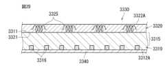
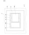
(積層型半導体パッケージ1の構成)
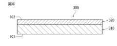
図1は、積層型半導体パッケージの第1実施形態を示す簡略断面図である。図1に示すように、積層型半導体パッケージ1は、第1基板210と、第1基板210に対して第1方向D1に積層される三次元デバイス300とを備える。第1方向D1は、図中、上方向とする。 First Embodiment
1. Overview of the structure (structure of stacked semiconductor package 1)
1 is a simplified cross-sectional view showing a first embodiment of a stacked semiconductor package. As shown in Fig. 1, the stacked semiconductor package 1 includes a
第1基板210は、例えば、SiやSiO2からなる無機基板(いわゆる、シリコンインターポーザ基板やガラスインターポーザ基板)であり、または、FR4(Flame Retardant Type 4)、エポキシ、ポリイミドなどからなる有機基板(いわゆる、有機パッケージ基板)などである。第1基板210の内部や主面には配線が設けられ、三次元デバイス300と電気的に接続される。第1基板210の主面には、外部端子、導電体バンプ、導電体ピラー、半田などの導電部材が設けられていてもよい。三次元デバイス300の第1基板210と対向する主面においても同様の導電部材が設けられていてもよい。The
三次元デバイス300は、第1方向D1に互いに積層される半導体集積回路部品310と受動部品320を有する。半導体集積回路部品310は、例えば、IC(Integrated Circuit)、CPU(Central Processing Unit)、PMIC(Power Management IC)、メモリ、トランジスタなどの電子部品である。受動部品320は、抵抗、コンデンサ、インダクタなどの電子部品であり、トランジスタのような能動素子を含まない。受動部品320の受動素子は、抵抗素子、コンデンサ素子、インダクタ素子などである。つまり、受動部品とは、素体、内部配線等を含み、受動素子とは、例えば受動部品内のコイル等を表し、素体等を含まない。半導体集積回路部品310と受動部品320の第1方向D1の積層の順番は、どちらが先でもよい。The three-
第1基板210の三次元デバイス300に対向する第1主面211と、三次元デバイス300の第1基板210に対向する第1主面301とは、離隔した状態で、第1接続部材5を介して接続される。第1接続部材5は、例えば、半田、導電体バンプ、導電体ピラーなどである。第1接続部材5は、複数あり、複数の第1接続部材5の少なくとも一部が、導電性を有していればよく、複数の第1接続部材5の一部が、絶縁性を有していてもよい。The first
半導体集積回路部品310の受動部品320に対向する第1主面311は、平坦面311aを含む。受動部品320の半導体集積回路に対向する第1主面321は、平坦面321aを含む。平坦面311a、321aは、それぞれ、平坦な面である。半導体集積回路部品310の平坦面311aと受動部品320の平坦面321aとは、接触した状態で、接合される。The first
上記構成によれば、半導体集積回路部品310の平坦面311aと受動部品320の平坦面321aとは、接触した状態で、接合されるので、三次元デバイス300の厚みを薄くでき、積層型半導体パッケージ1の薄型化を図ることができる。また、受動部品320を有するので、ノイズ除去や電源制御をさらに容易に行うことができる。According to the above configuration, the
この明細書では、「半導体集積回路部品310の平坦面311aの平坦」とは、平坦面311aの表面粗さが、半導体集積回路部品310の厚みの1/1000以下もしくは10nm以下のいずれかより小さい状態を示し、「受動部品320の平坦面321aの平坦」とは、平坦面321aの表面粗さが、受動部品320の厚みの1/1000以下もしくは10nm以下のいずれかより小さい状態を示す。各部材の厚みとは、各部材の第1方向D1における大きさをいう。In this specification, "flatness of
「表面粗さ」とは、Sa(算術平均高さ)である。平坦とは、例えばSaが0.2nmである状態をいう。Saの測定には、原子間力顕微鏡(AFM:Atomic Force Microscope)を用いる。表面粗さは、部品表面の5点におけるSaの平均値である。平坦面311a、321aを互いに分離することができる場合、かかる方法を用いることができるが、平坦面311a、321aを分離することができない場合、三次元デバイスの断面から表面粗さを算出してもよい。具体的に述べると、平坦面311a、321aの接合部分の断面をイオンミリングなど公知の方法で露出させ、接合部分を透過電子顕微鏡(TEM:Transmission Electron Microscope)などで画像取得する。このとき倍率は300K以上が好ましい。平坦面311a、321aの界面は、粒界の違いなどから認識できる。取得した画像を用いて、界面に対応する位置に直線(最小二乗法で引かれる線)を引く。この直線に対してRa(算術平均粗さ)を測定して、表面粗さを求めることができる。"Surface roughness" refers to Sa (arithmetic mean height). Flatness refers to a state in which Sa is 0.2 nm, for example. An atomic force microscope (AFM: Atomic Force Microscope) is used to measure Sa. The surface roughness is the average value of Sa at five points on the surface of the component. If the
また、「平坦面311a、321aの接合」とは、原子拡散やイオン結合による常温直接接合や、熱を加えたハイブリッド接合などをいう。また、「接合」とは、共有結合、イオン結合、金属結合などの化学的結合状態を指してもよいし、機械強度的な結合状態を指してもよい。接合強度の測定方法として、例えば、半導体集積回路部品の平坦面に受動部品の平坦面を接合し、半導体集積回路部品と受動部品のそれぞれを固定し、例えばボンドテスターなどで接合された平坦面に対して垂直な力をかけ、その接合強度を測定する方法がある。あるいは、接合された平坦面よりも上に押し治具をあてるようにし、横押しで接合強度を測定してもよい。接合強度は、1N以上あれば密着しているとした。1N以上であれば、振動及びハンドリング、例えばピンセットの横押しなどで剥がれることはない。また、接合強度は、固着力でなく、破壊モードで判断してもよい。接合された平坦面以外での破壊、俗に言われるバルク破壊が起これば接合強度は十分強いといえる。The "bonding of the
また、「第1基板210の第1主面211と三次元デバイス300の第1主面301とが離隔している」とは、第1基板210の第1主面211と三次元デバイス300の第1主面301とが、互いに平行な状態で離隔していることを指す。「平行」とは、一般的な製造ばらつきの範囲での平行を含む。具体的に述べると、第1基板210の第1主面211と三次元デバイス300の第1主面301とのなす角度は、10°以下である。また、第1基板210の第1主面211と三次元デバイス300の第1主面301とのいずれもが反っている場合、最小二乗法から求まる面を用いて第1主面211と第1主面301の間の距離(図1の第2距離L2に相当)を求める。第2距離L2は、積層型半導体パッケージ1に断面研磨等を行うことによって得られる特定の断面における第1基板210の第1主面211と三次元デバイス300の第1主面301の平均距離を表す。第1主面211と第1主面301の間の距離は、例えば、20μmである。なお、第1主面211と第1主面301の間に、アンダーフィルやモールド樹脂材などを充填してもよい。In addition, "the first
(積層型半導体パッケージ1の製造方法)
次に、積層型半導体パッケージ1の製造方法について説明する。 (Method of Manufacturing Stacked Semiconductor Package 1)
Next, a method for manufacturing the stacked semiconductor package 1 will be described.
図1に示すように、半導体集積回路部品310の第1主面311を研磨して平坦面311aを設ける。また、受動部品320の第1主面321を研磨して平坦面321aを設ける。その後、半導体集積回路部品310の平坦面311aと受動部品320の平坦面321aとを接触した状態で接合して、三次元デバイス300を形成する。その後、三次元デバイス300の第1主面301と第1基板210の第1主面211とを離隔した状態で第1接続部材5を介して接続する。As shown in FIG. 1, the first
これによれば、半導体集積回路部品310の平坦面311aと受動部品320の平坦面321aとを、接触した状態で、接合するので、三次元デバイス300の厚みを薄くでき、積層型半導体パッケージ1の薄型化を図ることができる。In this way, the
なお、複数の半導体集積回路部品を含む半導体基板と、複数の受動部品を含む受動基板とを用意し、半導体基板と受動基板を接合してから、一組の半導体集積回路部品および受動部品ごとに個片化して、複数の積層型半導体パッケージを形成してもよい。または、半導体基板と受動基板の一方の基板を部品ごとに個片化し、個片化した部品を半導体基板と受動基板の他方の基板に接合し、その後、他方の基板を部品ごとに個片化して、複数の積層型半導体パッケージを形成してもよい。A semiconductor substrate including a plurality of semiconductor integrated circuit components and a passive substrate including a plurality of passive components may be prepared, the semiconductor substrate and the passive substrate may be bonded together, and then each set of semiconductor integrated circuit components and passive components may be singulated to form a plurality of stacked semiconductor packages. Alternatively, one of the semiconductor substrate and the passive substrate may be singulated into individual components, the singulated components may be bonded to the other of the semiconductor substrate and the passive substrate, and then the other substrate may be singulated into individual components to form a plurality of stacked semiconductor packages.
2.好ましい形態
(積層型半導体パッケージ1の構成)
図1に示すように、第1基板210は、その第1主面211と反対側の第2主面212を有する。三次元デバイス300は、その第1主面301と反対側の第2主面302を有する。半導体集積回路部品310は、その第1主面311と反対側の第2主面312を有する。受動部品320は、その第1主面321と反対側の第2主面322を有する。 2. Preferred embodiment (Structure of stacked semiconductor package 1)
1 , the
三次元デバイス300の第1主面301は、半導体集積回路部品310の第2主面312と一致する。三次元デバイス300の第2主面302は、受動部品320の第2主面322と一致する。受動部品320は、半導体集積回路部品310に対して第1方向D1に積層される。The first
半導体集積回路部品310と受動部品320は、平坦面311a、321aを介して、電気的に接続される。これにより、平坦面311a、321aは、機械的接続と電気的接続を同時に満たすことができる。なお、半導体集積回路部品310と受動部品320とは、電気的に接続されなくてもよく、回路設計の自由度を向上できる。The semiconductor integrated
好ましくは、半導体集積回路部品310の平坦面311aの面積は、半導体集積回路部品310の第1主面311の面積の半分よりも大きく、受動部品320の平坦面321aの面積は、受動部品320の第1主面321の面積の半分よりも大きい。これによれば、平坦面の面積を大きくすることで、不要な凹凸を減少して、三次元デバイス300の厚みをより薄くできる。Preferably, the area of the
第1主面311の少なくとも一部が、平坦面311aであればよい。ただし、平坦面311aの面積が小さいと、部品310、320の間の密着力は低下するので、第1主面311の面積の半分以上が、平坦面311aであることが好ましい。同様に、第1主面321の少なくとも一部が、平坦面321aであればよく、第1主面321の面積の半分以上が、平坦面321aであることが好ましい。At least a portion of the first
対向する平坦面311a、321aの位置は、一般的な製造工程上許される程度にずれていてもよい。例えば、それぞれの平坦面に露出している配線同士を接触する場合、平坦面311a、321aのずれがない状態の配線の接触面積を基準にして、この基準の接触面積が50%に減少するまでの平坦面311a、321aのずれは、製造工程上許される範囲内とする。The positions of the opposing
好ましくは、半導体集積回路部品310の平坦面311aおよび受動部品320の平坦面321aは、それぞれ、無機物からなる。無機物は、例えば、Cu、Al、Au、Ti、Ta、Si、Ge、GaN、GaP、GaAs、InP、SiN、TiN、SiO2などである。これによれば、平坦面311a、321aが有機物からなる場合と比較して、平坦面311a、321aを平坦化しやすい。また、平坦面311a、321aのそれぞれの硬度は高く、三次元デバイス300の強度を強くすることができる。Preferably, the
平坦面311a、321aのそれぞれの無機物の材料は、同一であってもよく、または、異なっていてもよい。また、同一の平坦面311a、321aの一部分の無機物の材料と、同一の平坦面311a、321aの他の部分の無機物の材料とが、異なっていてもよい。例えば、受動部品320の平坦面321aにおいて、平坦面321aの一部分が、受動素子の引出配線の表面から構成され、平坦面321aの他の部分が、Siを含む絶縁層の表面から構成されていてもよい。The inorganic materials of the
半導体集積回路部品310のうちの少なくとも平坦面311aのみが、無機物からなっていればよく、半導体集積回路部品310のその他の部分が、有機物からなっていてもよい。同様に、受動部品320のうちの少なくとも平坦面321aのみが、無機物からなっていればよく、受動部品320のその他の部分が、有機物からなっていてもよい。At least the
図1に示すように、積層型半導体パッケージ1は、さらに、第2基板220を備える。第1基板210は、第2基板220に対して第1方向D1に積層される。第1基板210の第2基板220に対向する第2主面212と、第2基板220の第1基板210に対向する第1主面221とは、離隔し、第2接続部材6を介して接続される。第2接続部材6は、第1接続部材5と同様の材料である。As shown in FIG. 1, the stacked semiconductor package 1 further includes a
第1基板210の第2主面212と第2基板220の第1主面221との間の第1距離L1は、第1基板210の第1主面211と三次元デバイス300の第1主面301との間の第2距離L2よりも大きい。これによれば、回路システムを大型化でき、回路設計の自由度を向上できる。The first distance L1 between the second
「第1基板210の第2主面212と第2基板220の第1主面221とが離隔している」とは、第1基板210の第2主面212と第2基板220の第1主面221とが、互いに平行な状態で離隔していることを指す。「平行」とは、一般的な製造ばらつきの範囲での平行を含む。具体的に述べると、第1基板210の第2主面212と第2基板220の第1主面221とのなす角度は、10°以下である。また、第1基板210の第2主面212と第2基板220の第1主面221とのいずれもが反っている場合、最小二乗法から求まる面を用いて第2主面212と第1主面221の間の第1距離L1を求める。第1距離L1とは、積層型半導体パッケージ1に断面研磨等を行うことによって得られる特定の断面における第1基板210の第2主面212と第2基板220の第1主面221の平均距離を表す。第1距離L1は、例えば、300μmである。なお、第2主面212と第1主面221の間に、アンダーフィルやモールド樹脂材などを充填してもよい。"The second
第2基板220は、第1基板210よりも、設計精度が低い(粗い)。言い換えると、第2基板220上に設けられる第2接続部材6は、第1基板210上に設けられる第1接続部材5よりも大きくなる。このため、第2基板220と第1基板210の間に接続される第2接続部材6の高さは、第1基板210と三次元デバイス300の間に接続される第1接続部材5の高さよりも高くなる。つまり、第1距離L1は、第2距離L2よりも大きくなる。このように、第1基板210と第2基板220の設計精度の違いは、接続部材5、6の大きさの違い、つまり、第1距離L1と第2距離L2の大きさの違いと関連している。設計精度が微細であると、距離が小さくなり、設計精度が粗くなると、距離が大きくなる。The
(積層型半導体パッケージ1の製造方法)
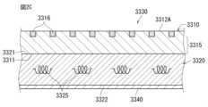
次に、図2Aから図2Gを用いて積層型半導体パッケージ1の製造方法を説明する。図2Aから図2Eでは、便宜上、図2Fと図2Gと比べて、三次元デバイスのアスペクト比(縦横比)を変更している。図2Aから図2Eでは、便宜上、図2Fと比べて、配線3316の数量を変更している。 (Method of Manufacturing Stacked Semiconductor Package 1)
Next, a method for manufacturing the stacked semiconductor package 1 will be described with reference to Figures 2A to 2G. For convenience, the aspect ratio of the three-dimensional device is changed in Figures 2A to 2E compared to Figures 2F and 2G. For convenience, the number of
図2Aに示すように、複数の半導体集積回路部品を含む半導体基板3310と複数の受動部品を含む受動基板3320を用意する。半導体基板3310は、半導体素子領域からなるデバイス層、つまり活性層3315と、活性層3315から信号を取り出したり、電力を供給するための複数の配線3316とを含む。配線3316は、図2AのようにTSV(through Si Via)などの公知の記述で基板厚み方向に延びる配線であってもよいし、BEOL(back-end-of-line)配線のように半導体基板面上に積層していてもよい。受動基板3320は、複数の受動素子3325を含む。図2Aでは、受動素子3325をインダクタ素子としている。半導体基板3310は、互いに反対側に位置する第1主面3311と第2主面3312を含む。受動基板3320は、互いに反対側に位置する第1主面3321と第2主面3322を含む。半導体基板3310の第1主面3311を研磨して平坦面3311aを設ける。また、受動基板3320の第1主面3321を研磨して平坦面3321aを設ける。本例では、CMP(Chemical Mechanical Polisher)研磨を用いた。As shown in FIG. 2A, a
図2Bに示すように、半導体基板3310の平坦面3311aと受動基板3320の平坦面3321aとを接触した状態で接合して、積層体3330を形成する。図2Cに示すように、受動基板3320の第2主面3322にテープ3340を貼り付け図示しない基台に固定して、半導体基板3310の第2主面3312(図2B参照)側を研磨して新たな第2主面3312Aを形成する。半導体基板3310の第2主面3312Aに、配線3316に接続する図示しない外部端子を形成する。その後、受動基板3320の第2主面3322のテープ3340を剥がす。As shown in FIG. 2B, the
図2Dに示すように、半導体基板3310の第2主面3312Aにテープ3340を貼り付け図示しない基台に固定して、受動基板3320の第2主面3322(図2C参照)側を研削して新たな第2主面3322Aを形成する。その後、半導体基板3310の第2主面3312Aのテープ3340を剥がす。As shown in FIG. 2D,
図2Eに示すように、積層体3330を一組の半導体集積回路部品310および受動部品320ごとにカット線Cにて個片化して、一組の半導体集積回路部品310および受動部品320から構成される三次元デバイス300を複数形成する。As shown in FIG. 2E, the
図2Fに示すように、第1基板210を準備し、第1基板210の第1主面211に第1接続部材5を設ける。その後、図2Gに示すように、三次元デバイス300の第1主面301と第1基板210の第1主面211とを離隔した状態で第1接続部材5を介して接続する。三次元デバイス300の第1主面301は、半導体基板3310の第2主面3312Aに相当し、三次元デバイス300の第2主面302は、受動基板3320の第2主面3322Aに相当する。半導体集積回路部品310の配線3316を第1接続部材5に接続する。As shown in FIG. 2F, the
その後、図1に示すように、第2基板220を準備し、第2基板220の第1主面221に接続部材6を設け、第1基板210の第2主面212と第2基板220の第1主面221を離隔した状態で接続部材6を介して接続する。これにより、積層型半導体パッケージ1を製造する。Then, as shown in FIG. 1, a
(積層型半導体パッケージ1の製造方法の変形例)
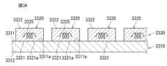
次に、図3Aから図3Cを用いて積層型半導体パッケージ1の製造方法の変形例を説明する。図3Aと図3Bでは、便宜上、図3Cと比べて、三次元デバイスのアスペクト比(縦横比)を変更している。 (Modification of the Manufacturing Method of the Stacked Semiconductor Package 1)
Next, a modified example of the manufacturing method of the stacked semiconductor package 1 will be described with reference to Figures 3A to 3C. For convenience, the aspect ratio of the three-dimensional device is changed in Figures 3A and 3B compared to Figure 3C.
図3Aに示すように、複数の半導体集積回路部品を含む半導体基板3310と受動部品を含む複数の受動基板3320を用意する。半導体基板3310は、上述したように活性層と複数の配線とを含む。受動基板3320は、受動素子3325を含む。半導体基板3310は、互いに反対側に位置する第1主面3311と第2主面3312を含む。受動基板3320は、互いに反対側に位置する第1主面3321と第2主面3322を含む。半導体基板3310の第1主面3311を研磨して平坦面3311aを設ける。また、受動基板3320の第1主面3321を研磨して平坦面3321aを設ける。その後、半導体基板3310の平坦面3311aと受動基板3320の平坦面3321aとを接触した状態で接合して、積層体3330を形成する。3A, a
その後、受動基板3320の第2主面3322側を研削して、図3Bに示すように、受動基板3320の新たな第2主面3322Aを形成する。その後、積層体3330を一組の半導体集積回路部品310および受動部品320ごとにカット線Cにて個片化して、一組の半導体集積回路部品310および受動部品320から構成される三次元デバイス300を複数形成する。図3Cに示すように、三次元デバイス300の第1主面301は、半導体基板3310の第2主面3312に相当し、三次元デバイス300の第2主面302は、受動基板3320の第2主面3322Aに相当する。Then, the second
その後、図1に示すように、三次元デバイス300の第1主面301と第1基板210の第1主面211とを離隔した状態で第1接続部材5を介して接続する。そして、第1基板210の第2主面212と第2基板220の第1主面221を離隔した状態で接続部材6を介して接続する。これにより、積層型半導体パッケージ1を製造する。After that, as shown in FIG. 1, the first
3.受動部品の好ましい形態
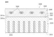
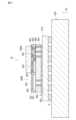
(インダクタ部品3の概略構成)
受動部品320は、好ましくは、インダクタ部品3である。図4は、インダクタ部品3を底面側から見た模式底面図である。図5は、図4のV-V断面図である。図6は、図4のVI-VI断面図である。なお、便宜上、図4では、素体10は、構造を容易に理解できるよう、透明に描かれているが、半透明や不透明であってもよい。また、図4では、絶縁体および無機層を省略して描いている。 3. Preferred form of passive component (general configuration of inductor component 3)
The
インダクタ部品3は、例えば、高周波信号伝送回路に用いられる表面実装型のインダクタ部品である。図4と図5と図6に示すように、インダクタ部品3は、素体10と、素体10に設けられ、軸AXに沿って螺旋状に巻き回されたコイル110と、素体10の第1主面(底面100b)に設けられた無機層21と、素体10の第2主面(天面100t)に設けられた絶縁体22とを備える。無機層21の底面21aが、受動部品320の第1主面321の平坦面321aに相当する。The
素体10は、長さ、幅および高さを有する。素体10は、長さ方向の両端側にある第1端面100e1および第2端面100e2と、幅方向の両端側にある第1側面100s1および第2側面100s2と、高さ方向の両端側にある底面100bおよび天面100tとを有する。つまり、素体10の外面100は、第1端面100e1および第2端面100e2と、第1側面100s1および第2側面100s2と、底面100bおよび天面100tとを含む。The
なお、図面に示すように、以下では、説明の便宜上、素体10の長さ方向(長手方向)であって、第1端面100e1から第2端面100e2に向かう方向をX方向とする。また、素体10の幅方向であって、第1側面100s1から第2側面100s2に向かう方向をY方向とする。また、素体10の高さ方向であって、底面100bから天面100tに向かう方向をZ方向とする。X方向、Y方向及びZ方向は、互いに直交する方向であって、X,Y,Zの順に並べたとき、右手系を構成する。As shown in the drawings, for the sake of convenience, the lengthwise direction (longitudinal direction) of the
この明細書では、素体10の第1端面100e1、第2端面100e2、第1側面100s1、第2側面100s2、底面100bおよび天面100tを含む「素体の外面100」は、単に素体10の外周側を向く面という意味ではなく、素体10の外側と内側との境界となる面である。また、「素体10の外面100の上方」とは、重力方向に規定される鉛直上方のような絶対的な一方向ではなく、外面100を基準に、当該外面100を境界とする外側と内側とのうち、外側に向かう方向を指す。したがって、「外面100の上方」とは外面100の向きによって定まる相対的な方向である。また、ある要素に対して「上方(above)」には、当該要素とは離れた上方、すなわち当該要素上の他の物体を介した上側の位置や間隔を空けた上側の位置だけではなく、当該要素と接する直上の位置(on)も含む。In this specification, the "
コイル110の軸AXは、底面100bに平行に配置される。コイル110は、軸AXに対して底面100b側に設けられ、底面100bに平行な平面上に軸AXに沿って配列された複数の第1コイル配線(底面配線11b)と、軸AXに対して天面100t側に設けられ、天面100tに平行な平面上に軸AXに沿って配列された複数の第2コイル配線(天面配線11t)と、底面配線11bから天面配線11tに向かって延在し、軸AXに沿って配列された複数の第1貫通配線13と、底面配線11bから天面配線11tに向かって延在し、軸AXに対して第1貫通配線13と反対側に設けられ、軸AXに沿って配列された複数の第2貫通配線14とを含む。底面配線11bと、第1貫通配線13と、天面配線11tと、第2貫通配線14とは、この順に接続されることにより、螺旋状の少なくとも一部を構成する。The axis AX of the
軸AXは、底面配線11bと天面配線11tの間の中央を通る第1平面と、第1貫通配線13と第2貫通配線14の間の中央を通る第2平面との交線をいう。つまり、軸AXは、コイル110の内径部の中心を通る直線である。コイル110の軸AXは、軸AXに直交する方向の寸法を有さない。The axis AX is the intersection of a first plane passing through the center between the
(インダクタ部品3)
インダクタ部品3の体積は、0.08mm3以下であり、かつ、インダクタ部品3の長辺の大きさは、0.65mm以下である。インダクタ部品3の長辺の大きさは、インダクタ部品3の長さ、幅および高さのうちの最も大きい値をいい、この実施形態では、X方向の長さをいう。上記構成によれば、インダクタ部品3の体積が小さく、かつ、インダクタ部品3の長辺も短いので、インダクタ部品3の重量が軽くなる。このため、外部電極121,122が小さくても、必要な実装強度を得ることができる。また、インダクタ部品3の厚みは、好ましくは、200μm以下である。これによれば、インダクタ部品3を薄くできる。 (Inductor component 3)
The volume of the
具体的に述べると、インダクタ部品3のサイズ(長さ(X方向)×幅(Y方向)×高さ(Z方向))は、0.6mm×0.3mm×0.3mm、0.4mm×0.2mm×0.2mm、0.25mm×0.125mm×0.120mmなどである。また、幅と高さは等しくなくてもよく、例えば、0.4mm×0.2mm×0.3mmなどであってもよい。Specifically, the size of the inductor component 3 (length (X direction) x width (Y direction) x height (Z direction)) is 0.6 mm x 0.3 mm x 0.3 mm, 0.4 mm x 0.2 mm x 0.2 mm, 0.25 mm x 0.125 mm x 0.120 mm, etc. Furthermore, the width and height do not have to be equal, and may be, for example, 0.4 mm x 0.2 mm x 0.3 mm.
(素体10)
素体10は、絶縁樹脂から構成される。絶縁樹脂としては、例えば、感光性永久膜(永久フォトレジスト)や、無機フィラーを含有した絶縁樹脂を用いる。感光性永久膜とは、加工処理をした後、取り除かないフォトレジストである。 (Element 10)
The
なお、素体10は、例えば、ガラス焼結体から構成されていてもよく、または、ガラス基板から構成されてもよい。ガラス基板は、単層のガラス基板であってもよく、素体の大部分がガラスとなることから、高周波での渦電流損のような損失を抑制することができる。The
(コイル110)
コイル110は、複数の底面配線11bと、複数の天面配線11tと、複数の第1貫通配線13と、複数の第2貫通配線14とを備える。底面配線11b、第1貫通配線13、天面配線11tおよび第2貫通配線14は、順に接続されて軸AX方向に巻き回されたコイル110の少なくとも一部を構成する。 (Coil 110)
The
上記構成によれば、コイル110は、いわゆるヘリカル形状のコイル110であるので、軸AXに直交する断面において、底面配線11b、天面配線11t、第1貫通配線13および第2貫通配線14がコイル110の巻き回し方向に沿って並走する領域を低減でき、コイル110における浮遊容量を低減できる。According to the above configuration, the
ここで、ヘリカル形状とは、コイル全体のターン数は1ターンより大きく、かつ、軸に直交する断面におけるコイルのターン数は1ターン未満である形状をいう。1ターン以上とは、軸に直交する断面において、コイルの配線が、軸方向からみて径方向に隣り合って巻回方向に並走する部分を有する状態をいい、1ターン未満とは、軸に直交する断面において、コイルの配線が、軸方向からみて径方向に隣り合って巻回方向に並走する部分を有さない状態をいう。Here, a helical shape refers to a shape in which the number of turns in the entire coil is greater than one turn, and the number of turns in the coil in a cross section perpendicular to the axis is less than one turn. "One or more turns" refers to a state in which, in a cross section perpendicular to the axis, the coil wiring has parts that are adjacent in the radial direction when viewed from the axial direction and run parallel to the winding direction, and "less than one turn" refers to a state in which, in a cross section perpendicular to the axis, the coil wiring does not have parts that are adjacent in the radial direction when viewed from the axial direction and run parallel to the winding direction.
底面配線11bは、ややX方向に傾いてY方向に延伸している。底面配線11bは、底面100bから露出するように素体10に埋め込まれている。複数の底面配線11bは、X方向に沿って平行に配置されている。底面100bに直交する方向からみて、軸AX方向の両端の底面配線11bは、三角形状に形成され、その他の底面配線11bは、直線形状に形成されている。The
天面配線11tは、Y方向に延びる形状である。天面配線11tは、天面100t上に設けられている。複数の天面配線11tは、X方向に沿って平行に配置されている。底面100bに直交する方向からみて、軸AX方向の両端の天面配線11tは、四角形状に形成され、その他の天面配線11tは、直線形状に形成されている。The
底面配線11bおよび天面配線11tは、銅、銀,金又はこれらの合金などの良導体材料からなる。底面配線11bおよび天面配線11tは、めっき、蒸着、スパッタリングなどによって形成された金属膜であってもよいし、導体ペーストを塗布、焼結させた金属焼結体であってもよい。また、底面配線11bおよび天面配線11tは、複数の金属層が積層された多層構造であってもよい。底面配線11bおよび天面配線11tの厚みは、5μm以上50μm以下であることが好ましい。The
第1貫通配線13は、素体10の貫通孔V内で、軸AXに対して第1側面100s1側に配置され、第2貫通配線14は、素体10の貫通孔V内で、軸AXに対して第2側面100s2側に配置されている。第1貫通配線13および第2貫通配線14は、それぞれ、底面100bおよび天面100tに直交する方向に延伸している。これによれば、第1貫通配線13および第2貫通配線14の長さを短くできるため、直流抵抗(Rdc)を抑制できる。全ての第1貫通配線13および全ての第2貫通配線14は、それぞれ、X方向に沿って平行に配置されている。第1貫通配線13および第2貫通配線14は、底面配線11bおよび天面配線11tと同様の材料から構成される。The first through
(無機層21)
無機層21は、素体10の底面100bに設けられ、底面配線11bの底面100bからの露出部分を覆う。これにより、底面配線11bを外力から保護し、底面配線11bの損傷を防止し、底面配線11bの絶縁性を向上する。無機層21は、無機物からなる。無機物は、例えば、Cu、Al、Au、Ti、Ta、Si、Ge、GaN、GaP、GaAs、InP、SiN、TiN、SiO2などである。無機層21の底面21aが、受動部品320の第1主面321の平坦面321aに相当する。 (Inorganic layer 21)
The
(絶縁体22)
絶縁体22は、素体10の天面100tに設けられ、天面配線11tを覆う。これにより、天面配線11tを外力から保護し、天面配線11tの損傷を防止し、天面配線11tの絶縁性を向上する。絶縁体22は、好ましくは、有機絶縁体である。例えば、絶縁体22は、形成が容易なエポキシ系、ポリイミド系樹脂などの樹脂膜であってもよい。 (Insulator 22)
The
(第1ビア配線121vおよび第2ビア配線122v)
インダクタ部品3は、さらに、第1ビア配線121vおよび第2ビア配線122vを有する。第1ビア配線121vは、コイル110の第1端部に接続され、第2ビア配線122vは、コイル110の第2端部に接続される。 (First via
The
第1ビア配線121vは、素体10のX方向の中心に対して第1端面100e1側に設けられている。第2ビア配線122vは、素体10のX方向の中心に対して第2端面100e2側に設けられている。The first via
第1ビア配線121vは、無機層21に埋め込まれ、無機層21の底面21aから露出する。第1ビア配線121vは、軸AX方向の第1端面100e1側に位置する底面配線11bの端部に接続される。The first via
第2ビア配線122vは、無機層21に埋め込まれ、無機層21の底面21aから露出する。第2ビア配線122vは、軸AX方向の第2端面100e2側に位置する底面配線11bの端部に接続される。The second via
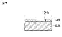
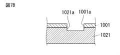
(インダクタ部品3の製造方法)
次に、図7Aから図7Kを用いてインダクタ部品3の製造方法を説明する。図7A、図7B、図7C、図7J、図7Kは、図4のVI-VI断面に対応した図である。図7D~図7Iは、図4のV-V断面に対応した図である。 (Method of Manufacturing Inductor Component 3)
Next, a manufacturing method of the
図7Aに示すように、無機層21に相当する無機基板1021を準備する。無機基板1021は、例えば、Si基板である。無機基板1021の上面に第1レジスト層1001を塗布し、フォトリソグラフィ工程により、第1レジスト層1001に所定パターンの開口部1001aを形成する。As shown in FIG. 7A, an
図7Bに示すように、開口部1001aを介して無機基板1021をエッチングして溝部1021aを形成する。エッチングは、ドライエッチングまたはウェットエッチングの何れであってもよい。本実施形態では、無機基板1021にSi基板を使用しているため、フッ素系ガスによるプラズマエッチングを用いる。As shown in FIG. 7B, the
その後、第1レジスト層1001を剥離して、図7Cと図7Dに示すように、無機基板1021の上面に図示しないシード層を形成し、シード層の上面に第2レジスト層1002を塗布して、フォトリソグラフィ工程により、第2レジスト層1002に所定パターンの開口部1002aを形成する。そして、電解めっきにより、開口部1002aに底面配線11bに相当する底面導体層1011bを設け、溝部1021aに第1ビア配線121vに相当する第1ビア導体層1121vを設ける。また、図示しないが、第1ビア導体層1121vと同様に、第2ビア配線122vに相当する第2ビア導体層を設ける。Then, the first resist
本実施形態では、底面導体層およびビア導体層の形成方法として、セミアディティブ法を用いるが、サブトラクティブ法、フルアディティブ法、または、導電ペーストの印刷法などの公知の方法を用いてもよい。本実施形態では、シード層に、Ti/Cuを用いるが、WやTiW、Agなど必要に応じてシード種およびその組み合わせを選択してよい。In this embodiment, a semi-additive method is used as a method for forming the bottom conductor layer and the via conductor layer, but known methods such as a subtractive method, a full additive method, or a conductive paste printing method may also be used. In this embodiment, Ti/Cu is used for the seed layer, but seed types and combinations thereof such as W, TiW, and Ag may be selected as necessary.
その後、第2レジスト層1002を剥離し、シード層をエッチングして、図7Eに示すように、無機基板1021の上面に素体10に相当する絶縁樹脂層1010を設ける。フォトリソグラフィ工程により、絶縁樹脂層1010に所定パターンの開口部1010aを形成し、開口部1010aから底面導体層1011bの一部を露出して、絶縁樹脂層1010を硬化する。本実施形態では、絶縁樹脂層1010に感光性永久膜を用いるが、例えば、無機フィラーを含有した絶縁樹脂をレーザ法やブラスト法により開口部を形成してもよく、または、CVDなどで無機絶縁層を蒸着させエッチング法などで開口部を形成してもよい。Then, the second resist
図7Fに示すように、絶縁樹脂層1010の開口部1010aに第2貫通配線14に相当する第2貫通導体層1014を形成する。また、図示しないが、第2貫通導体層1014と同様に、第1貫通配線13に相当する第1貫通導体層を設ける。具体的に述べると、本実施形態では、異方性スパッタを用いて絶縁樹脂層1010の上面および開口部1010a内面にTi/Cuのシード層を形成する。その後、フィルドめっきを行いCMPや機械研磨などにより絶縁樹脂層1010の上面を平坦化する。なお、貫通導体層の他の形成方法としては、底面導体層に予め通電部を設けておき、通電部から給電して電解めっき法により形成してもよい。As shown in FIG. 7F, a second through
その後、絶縁樹脂層1010の上面に図示しないシード層を形成し、シード層の上面に図示しないレジスト層を塗布して、フォトリソグラフィ工程により、レジスト層に所定パターンの開口部を形成する。そして、電解めっきにより、開口部に天面配線11tに相当する天面導体層1011tを設け、図7Gに示すように、レジスト層を剥離し、シード層をエッチングする。After that, a seed layer (not shown) is formed on the upper surface of the insulating
図7Hに示すように、絶縁樹脂層1010の上面に天面導体層1011tを覆うように絶縁体22に相当する絶縁層1022を設け、絶縁層1022を硬化する。絶縁層1022は、絶縁樹脂層1010と同じ樹脂であってもよく、または、異なる樹脂であってもよい。絶縁層1022は、外部と触れることから、絶縁樹脂層1010と比較して、耐水性に優れた樹脂や高硬度の樹脂を用いることが好ましく、さらに、無機フィラーなどを含有する樹脂を用いることが好ましく、これにより絶縁性が向上する。さらに、絶縁層1022は、絶縁樹脂層1010と比較して、遮光性(遮蔽性)が高い樹脂を用いることが好ましい。As shown in FIG. 7H, an insulating
図7Iと図7Jに示すように、無機基板1021を研磨して、第1ビア導体層1121vの端面および第2ビア導体層の端面を露出する。無機基板1021の研磨にはCMPが好ましい。なお、必要に応じて絶縁層1022を厚み調整のために研磨してもよい。As shown in Figures 7I and 7J, the
図7Kに示すように、カット線Cにて個片化する。これにより、図6に示すように、インダクタ部品3を製造する。As shown in FIG. 7K, the chip is cut into individual pieces along cut lines C. This produces
4.変形例
(第1変形例)
図8は、積層型半導体パッケージの第1変形例を示す簡略断面図である。図8に示すように、第1変形例の積層型半導体パッケージ1Aでは、図1の積層型半導体パッケージ1と比べて、三次元デバイス300Aの構成が相違する。その他の構成は、第1実施形態と同じ構成であり、その説明を省略する。 4. Modification (First Modification)
Fig. 8 is a simplified cross-sectional view showing a first modified example of a stacked semiconductor package. As shown in Fig. 8, in the stacked
図8に示すように、三次元デバイス300Aは、複数の集積回路部品401~403と、複数のインダクタ部品501~503と、複数のコンデンサ部品601、602とを有する。集積回路部品401~403は、特許請求の範囲の「半導体集積回路部品」の一例に相当し、例えば、第1実施形態の半導体集積回路部品310の一例に相当する。インダクタ部品501~503およびコンデンサ部品601、602は、特許請求の範囲の「受動部品」の一例に相当し、例えば、第1実施形態の受動部品320の一例に相当する。As shown in FIG. 8, the three-
複数の半導体集積回路部品(集積回路部品401~403)は、第1方向D1に並んで配置される。これによれば、回路設計の自由度を向上できる。具体的に述べると、第1集積回路部品401、第2集積回路部品402および第3集積回路部品403は、第1方向D1に順に積層されている。なお、複数の半導体集積回路部品は、第1方向D1または第1方向D1に直交する方向に並んで配置されていてもよい。The multiple semiconductor integrated circuit components (integrated
複数の受動部品(インダクタ部品501~503およびコンデンサ部品601、602)は、第1方向D1に並んで配置される。これによれば、回路設計の自由度を向上できる。具体的に述べると、第1インダクタ部品501、第2インダクタ部品502および第3インダクタ部品503は、第1方向D1に順に積層されている。第1コンデンサ部品601および第2コンデンサ部品602は、第1方向D1に順に積層されている。第1インダクタ部品501、第1コンデンサ部品601および第2コンデンサ部品602は、第1方向D1に順に積層されている。Multiple passive components (inductor components 501-503 and
第1インダクタ部品501は、第1集積回路部品401と第2集積回路部品402の間に位置する。第2インダクタ部品502と第1コンデンサ部品601は、第2集積回路部品402と第3集積回路部品403の間に位置する。第3インダクタ部品503と第2コンデンサ部品602は、第3集積回路部品403に積層される。The
複数の受動部品(インダクタ部品502、503およびコンデンサ部品601、602)は、第1方向D1に直交する方向に並んで配置される。これによれば、回路設計の自由度を向上できる。具体的に述べると、第2インダクタ部品502および第1コンデンサ部品601は、第1方向D1に直交する方向に並んで配置される。第3インダクタ部品503および第2コンデンサ部品602は、第1方向D1に直交する方向に並んで配置される。なお、複数の受動部品は、第1方向D1または第1方向D1に直交する方向に並んで配置されていてもよい。The multiple passive components (
ここで、第1集積回路部品401と第1インダクタ部品501の接合、第1インダクタ部品501と第2集積回路部品402の接合、第2集積回路部品402と第2インダクタ部品502の接合、第2集積回路部品402と第1コンデンサ部品601の接合、第2インダクタ部品502と第3集積回路部品403の接合、第1コンデンサ部品601と第3集積回路部品403の接合、第3集積回路部品403と第3インダクタ部品503の接合、第3集積回路部品403と第2コンデンサ部品602の接合は、第1実施形態で説明した互いの平坦面による直接接合である。Here, the bonding between the first
好ましくは、全ての半導体集積回路部品(集積回路部品401~403)および全ての受動部品(インダクタ部品501~503およびコンデンサ部品601、602)のうちの複数の部品は、同一層に積層され、複数の部品のそれぞれの厚みは、同じである。具体的に述べると、第2インダクタ部品502および第1コンデンサ部品601は、同一層に積層され、第2インダクタ部品502および第1コンデンサ部品601のそれぞれの厚みは、同じである。Preferably, all of the semiconductor integrated circuit components (integrated circuit components 401-403) and all of the passive components (inductor components 501-503 and
上記構成によれば、同一層の複数の部品(第2インダクタ部品502、第1コンデンサ部品601)のそれぞれの厚みは同じであるので、部品の積層数を増加しても、積層された部品の傾きを低減できる。また、同一層の一部の部品の厚みを不要に厚くしないので、積層型半導体パッケージ1Aの薄型化を図ることができる。なお、このとき、三次元デバイスは、少なくとも1つの半導体集積回路部品と少なくとも1つの受動部品とを有していればよい。According to the above configuration, the thickness of each of the multiple components (
好ましくは、全ての半導体集積回路部品(集積回路部品401~403)および全ての受動部品(インダクタ部品501~503およびコンデンサ部品601、602)のうちの複数の部品は、第1方向D1の最上層に積層され、最上層の複数の部品のうちの少なくとも2つの部品のそれぞれの厚みは、異なる。具体的に述べると、第3インダクタ部品503および第2コンデンサ部品602は、最上層に積層され、第3インダクタ部品503および第2コンデンサ部品602のそれぞれの厚みは、異なる。Preferably, all of the semiconductor integrated circuit components (integrated circuit components 401-403) and all of the passive components (inductor components 501-503 and
上記構成によれば、最上層の複数の部品のうちの少なくとも2つの部品(第3インダクタ部品503および第2コンデンサ部品602)のそれぞれの厚みは、異なるので、異なる厚みの部品を最上層に集積することができる。また、最上層の上方に部品を積層しないため、最上層の厚みの調整工程は不要となる。なお、このとき、三次元デバイスは、少なくとも1つの半導体集積回路部品と少なくとも1つの受動部品とを有していればよい。According to the above configuration, at least two of the multiple components on the top layer (the
なお、最上層に受動部品と半導体集積回路部品が存在するとき、受動部品の厚みが半導体集積回路部品の厚みよりも厚いことが好ましい。通常、半導体集積回路部品のアクティブエリア(活性層が形成されている領域)は非常に薄膜であり、設計精度が低い受動部品の厚みが一般的に厚くなる。そのため、受動部品を厚くすることで体積が大きくなりパッケージ全体のフットプリント(平面面積)を抑えつつ、高性能化できる。さらに、受動部品がインダクタ部品を有する場合、インダクタ部品の厚みが最も厚い。インダクタ部品はエネルギー貯蔵率がコンデンサ部品より一般的に小さいため、インダクタ部品の厚みを厚くして体積を大きくすることにより、パッケージ全体のフットプリントの縮小に寄与する。例えば、最上層の半導体集積回路部品の厚みは100μmであり、コンデンサ部品の厚みは220μmであり、インダクタ部品の厚みは330μmである。When passive components and semiconductor integrated circuit components are present on the top layer, it is preferable that the thickness of the passive components is thicker than that of the semiconductor integrated circuit components. Usually, the active area (area where the active layer is formed) of the semiconductor integrated circuit components is very thin, and the thickness of the passive components with low design accuracy is generally thick. Therefore, by making the passive components thicker, the volume increases, and it is possible to improve performance while suppressing the footprint (planar area) of the entire package. Furthermore, when the passive components include inductor components, the thickness of the inductor components is the thickest. Since the energy storage rate of inductor components is generally smaller than that of capacitor components, making the inductor components thicker to increase their volume contributes to reducing the footprint of the entire package. For example, the thickness of the semiconductor integrated circuit components on the top layer is 100 μm, the thickness of the capacitor components is 220 μm, and the thickness of the inductor components is 330 μm.
好ましくは、全ての半導体集積回路部品(集積回路部品401~403)および全ての受動部品(インダクタ部品501~503およびコンデンサ部品601、602)のうちの第1方向D1において第1基板210に最も近い部品の面積は、その他の部品のそれぞれの面積よりも大きい。部品の面積とは、第1方向D1に垂直な面の面積(平面の面積)をいう。具体的に述べると、第1基板210に最も近い第1集積回路部品401の面積は、好ましくは、その他の部品(第2と第3集積回路部品402、403、第1から第3インダクタ部品501~503および第1と第2コンデンサ部品601、602)のそれぞれの面積よりも大きい。Preferably, the area of the component closest to the
上記構成によれば、第1基板210に最も近い部品の面積(フットプリント)が最も大きいので、第1基板210に最も近い部品に積層する他の部品のアライメントズレを吸収でき、また、他の部品のカットに対するプロセスマージンを広くとることができる。なお、このとき、三次元デバイスは、少なくとも1つの半導体集積回路部品と少なくとも1つの受動部品とを有していればよい。According to the above configuration, the area (footprint) of the component closest to the
なお、さらに好ましくは、半導体集積回路部品および受動部品のそれぞれの面積が、第1方向D1に沿って順に、小さくなる。これによれば、各部品の積層工程において、各部品のアライメントズレを防止し、各部品のカットに対するプロセスマージンを確保することができる。More preferably, the areas of the semiconductor integrated circuit components and the passive components decrease in order along the first direction D1. This makes it possible to prevent misalignment of the components during the stacking process and ensure a process margin for cutting the components.
好ましくは、全ての受動部品(インダクタ部品501~503およびコンデンサ部品601、602)のうちの少なくとも1つの面積は、全ての半導体集積回路部品(集積回路部品401~403)の少なくとも1つの面積よりも小さい。具体的に述べると、第2インダクタ部品502および第3インダクタ部品503のそれぞれの面積は、第1から第3集積回路部品401~403のそれぞれの面積よりも小さい。第1コンデンサ部品601および第2コンデンサ部品602のそれぞれの面積は、第1から第3集積回路部品401~403のそれぞれの面積よりも小さい。Preferably, the area of at least one of all the passive components (inductor components 501-503 and
上記構成によれば、面積の小さい受動部品を半導体集積回路部品に積層することで、半導体集積回路部品の余ったスペースに他の機能を付与でき、三次元デバイスの集積度を向上できる。なお、このとき、三次元デバイスは、少なくとも1つの半導体集積回路部品と少なくとも1つの受動部品とを有していればよい。According to the above configuration, by stacking small-area passive components on semiconductor integrated circuit components, other functions can be added to the remaining space of the semiconductor integrated circuit components, thereby improving the integration density of the three-dimensional device. In this case, it is sufficient for the three-dimensional device to have at least one semiconductor integrated circuit component and at least one passive component.
好ましくは、上記の面積の小さい受動部品は、コンデンサ部品である。具体的に述べると、第1コンデンサ部品601および第2コンデンサ部品602のそれぞれの面積は、第1から第3集積回路部品401~403のそれぞれの面積よりも小さい。これによれば、効率的に集積度の高い三次元デバイスを提供できる。コンデンサ部品は、インダクタ部品に比べて、一般的に体積当たりのエネルギー貯蔵率が高いので、コンデンサ部品は小型化しやすい。Preferably, the small-area passive components are capacitor components. Specifically, the area of each of the
好ましくは、全ての受動部品(インダクタ部品501~503およびコンデンサ部品601、602)のうちの少なくとも1つの面積は、全ての半導体集積回路部品(集積回路部品401~403)の少なくとも1つの面積よりも大きい。具体的に述べると、第1インダクタ部品501の面積は、第3集積回路部品403の面積よりも大きい。Preferably, the area of at least one of all the passive components (inductor components 501-503 and
上記構成によれば、受動部品は、半導体集積回路部品に比べて、プロセスノード(デザインルール)が緩いため、受動部品の面積を大きくすることで、製造コストを低減できる。なお、このとき、三次元デバイスは、少なくとも1つの半導体集積回路部品と少なくとも1つの受動部品とを有していればよい。According to the above configuration, since passive components have looser process nodes (design rules) than semiconductor integrated circuit components, manufacturing costs can be reduced by increasing the area of the passive components. In this case, it is sufficient for the three-dimensional device to have at least one semiconductor integrated circuit component and at least one passive component.
好ましくは、上記の面積の大きい受動部品は、インダクタ部品である。これによれば、効率的に集積度の高い三次元デバイスを提供できる。インダクタ部品の面積を大きくすることで所望の回路定数を得られる。Preferably, the large-area passive component is an inductor component. This makes it possible to efficiently provide a highly integrated three-dimensional device. By increasing the area of the inductor component, the desired circuit constant can be obtained.
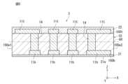
(第2変形例)
図9は、積層型半導体パッケージの第2変形例を示す簡略断面図である。図9に示すように、第2変形例の積層型半導体パッケージ1Bでは、図8の積層型半導体パッケージ1Aと比べて、三次元デバイス300Bの構成が相違し、また、三次元デバイス300B以外の他の部品を有する。その他の構成は、第1変形例と同じ構成であり、その説明を省略する。 (Second Modification)
Fig. 9 is a simplified cross-sectional view showing a second modified example of a stacked semiconductor package. As shown in Fig. 9, the stacked
図9に示すように、三次元デバイス300Bは、1つのインダクタ部品501と1つのコンデンサ部品601と1つの集積回路部品401とを有する。インダクタ部品501とコンデンサ部品601と集積回路部品401とは、第1方向D1に並んで配置される。コンデンサ部品601は、特許請求の範囲の「第1受動部品」の一例に相当し、インダクタ部品501は、特許請求の範囲の「第2受動部品」の一例に相当する。As shown in FIG. 9, the three-
インダクタ部品501のコンデンサ部品601に対向する第1主面501aと、コンデンサ部品601のインダクタ部品501に対向する第1主面601aとは、それぞれ、平坦面を含む。インダクタ部品501の平坦面とコンデンサ部品601の平坦面とは、接触した状態で、接合される。この接合は、第1実施形態で説明した互いの平坦面による直接接合である。同様に、コンデンサ部品601と集積回路部品401の接合は、互いの平坦面による直接接合である。The first
上記構成によれば、インダクタ部品501の平坦面とコンデンサ部品601の平坦面とは、接触した状態で、接合されるので、三次元デバイス300Bの厚みを薄くでき、積層型半導体パッケージ1Bの薄型化を図ることができる。なお、このとき、三次元デバイスは、複数の受動部品を有していればよい。According to the above configuration, the flat surface of the
積層型半導体パッケージ1Bは、実装用の集積回路部品400Aおよび実装用のインダクタ部品500Aを有する。ここで、実装用とは、平坦面により直接接合されたものでない部品をいう。具体的に述べると、実装用の集積回路部品400Aおよび実装用のインダクタ部品500Aは、第1基板210に実装される。実装用の集積回路部品400Aおよび実装用のインダクタ部品500Aは、第1接続部材5を介して、第1基板210の第1主面211に接続される。The stacked
上記構成によれば、第1基板210の同一の第1主面211には、三次元デバイス300B以外の集積回路部品400Aおよびインダクタ部品500Aを備えているので、パッケージの集積度を上げられるほか、寄生成分を抑制することができる。According to the above configuration, the same first
<第2実施形態>
(積層型半導体パッケージ1Cの構成)
図10Aは、積層型半導体パッケージの第2実施形態を示す簡略断面図である。図10Bは、積層型半導体パッケージの第2実施形態を示す簡略平面図である。なお、便宜上、図10Bでは、絶縁部材を省略して描いている。 Second Embodiment
(Configuration of stacked semiconductor package 1C)
10A and 10B are simplified cross-sectional and plan views showing a second embodiment of a stacked semiconductor package, respectively, in which an insulating member is omitted for convenience.
図10Aと図10Bに示すように、第2実施形態の積層型半導体パッケージ1Cでは、図1の積層型半導体パッケージ1と比べて、三次元デバイス300Cの構成が相違し、また、三次元デバイス300C以外の他の部品を有する。その他の構成は、第1実施形態と同じ構成であり、その説明を省略する。As shown in Figures 10A and 10B, the stacked semiconductor package 1C of the second embodiment differs from the stacked semiconductor package 1 of Figure 1 in that the configuration of the three-
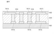
図10Aと図10Bに示すように、三次元デバイス300Cは、集積回路部品401と、インダクタ部品501と、第1コンデンサ部品601と、第2コンデンサ部品602と、第1絶縁部材701と、第2絶縁部材702とを有する。As shown in Figures 10A and 10B, the three-
集積回路部品401と第1コンデンサ部品601と第2コンデンサ部品602は、インダクタ部品501の同一の上面に積層される。集積回路部品401とインダクタ部品501の接合、第1コンデンサ部品601とインダクタ部品501の接合、および、第2コンデンサ部品602とインダクタ部品501の接合は、第1実施形態で説明した互いの平坦面による直接接合である。The
第1絶縁部材701は、集積回路部品401と第1コンデンサ部品601と第2コンデンサ部品602の少なくとも一部を覆うように、インダクタ部品501の上面に設けられている。これによれば、第1絶縁部材701により水分や機械的ストレスから部品を保護することができる。また、第1絶縁部材701上にさらに配線を設けることで積層数を増やし、配線の引き回しを可能とし、回路設計の自由度を向上できる。The first insulating
第1絶縁部材701は、例えば、エポキシ系樹脂、フェノール系樹脂、ポリイミド系樹脂、液晶ポリマー系樹脂などからなり、または、これらの樹脂などに無機フィラーを含有したコンポジット材などからなり、または、CVDや蒸着法などでSiやSiO2やSiNなどの無機物からなる。The first insulating
第2絶縁部材702は、第1絶縁部材701の上面に設けられている。第2絶縁部材702は、例えば、第1絶縁部材701と同様の材料からなる。The second insulating
三次元デバイス300Cは、さらに、三次元デバイス300Cの第2主面302に電気的接続部801を備える。具体的に述べると、第1主面301は、インダクタ部品501の下面から構成され、第2主面302は、第2絶縁部材702の上面から構成される。複数の電気的接続部801は、第2絶縁部材702を貫通するように設けられる。電気的接続部801は、例えば、外部端子である。複数の電気的接続部801は、複数のビア部802を介して、第1コンデンサ部品601および第2コンデンサ部品602のそれぞれに電気的に接続される。ビア部802は、第1絶縁部材701内に設けられている。The three-
上記構成によれば、他の部品を電気的接続部801上に積層しつつ電気的接続部に電気的に接続することができて、積層数を増やすことができ、積層の自由度や回路設計の自由度を向上できる。なお、電気的接続部801は、第1主面301および第2主面302の少なくとも一方に設けられていてもよい。According to the above configuration, other components can be stacked on the
好ましくは、積層型半導体パッケージ1Cは、さらに、実装用の集積回路部品400Aを有する。具体的に述べると、実装用の集積回路部品400Aは、第2絶縁部材702に実装される。実装用の集積回路部品400Aは、電気的接続部801を介して、第2絶縁部材702の上面に接続される。これによれば、三次元デバイス300C以外の集積回路部品400Aを備えているので、パッケージの集積度を上げられるほか、寄生成分を抑制することができる。Preferably, the stacked semiconductor package 1C further includes an
(変形例)
図11は、積層型半導体パッケージの変形例を示す簡略断面図である。図11に示すように、変形例の積層型半導体パッケージ1Dでは、図10Aの積層型半導体パッケージ1Cと比べて、三次元デバイス300Dの構成が相違する。その他の構成は、第2実施形態と同じ構成であり、その説明を省略する。 (Modification)
Fig. 11 is a simplified cross-sectional view showing a modified example of a stacked semiconductor package. As shown in Fig. 11, in the modified stacked
図11に示すように、三次元デバイス300Dは、図10Aの三次元デバイス300Cと比べて、第2コンデンサ部品602がなく、第1導通配線901および第2導通配線902を有する点が相違する。つまり、三次元デバイス300Dは、集積回路部品401と、インダクタ部品501と、コンデンサ部品601と、第1絶縁部材701と、第2絶縁部材702と、複数の第1導通配線901と、複数の第2導通配線902とを有する。As shown in FIG. 11, three-
第1絶縁部材701は、集積回路部品401およびコンデンサ部品601と同一層に積層されている。第1導通配線901は、第1絶縁部材701を貫通する。これによれば、回路設計の自由度を向上できる。また、第1導通配線901は、第1絶縁部材701を貫通するので、第1導通配線901を容易に形成できる。The first insulating
第1導通配線901は、例えば、CuもしくはCuを含む合金からなる。第1導通配線901は、好ましくは、半導体集積回路部品のFEOL(front-end-of-line)配線よりも断面積が大きい。さらに好ましくは、半導体集積回路部品のBEOL(back-end-of-line)配線よりも断面積が大きい。第1導通配線901の材料として比較的材料価格の安いCuを用い、かつ、第1導通配線901にラフなプロセスノードを用いることで、第1導通配線901を安価に形成することができる。第1導通配線901は、集積回路部品401の厚みまたはコンデンサ部品601の厚みと同等もしくはそれ以上であり、且つ第1絶縁部材701の厚みと同等もしくはそれ以下である。The first
第2導通配線902は、インダクタ部品501を貫通しインダクタ部品501のインダクタ素子に接続されない。インダクタ素子は、コイルを含む。これによれば、第2導通配線902によりインダクタ素子を介さないで電気信号を受け渡しでき、集積度を向上できる。The second
第2貫通配線902の材料は、例えば、第1導通配線901と同様の材料である。第2導通配線902は、好ましくは、半導体集積回路部品のFEOL配線よりも断面積が大きい。さらに好ましくは、半導体集積回路部品のBEOL配線よりも断面積が大きい。第2導通配線902は、インダクタ部品501の厚みと同等もしくはそれ以上である。なお、第2導通配線は、インダクタ部品501以外の他の受動部品を貫通し、他の受動部品の受動素子に接続されなくてもよい。The material of the second through-
第1導通配線901は、一部の第2導通配線902に電気的に接続される。実装用の集積回路部品400Aと第1基板210とは、第1導通配線901と一部の第2導通配線902を介して、電気的に接続される。集積回路部品401と第1基板210とは、他の第2導通配線902を介して、電気的に接続される。The first
<第3実施形態>
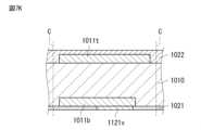
図12は、積層型半導体パッケージの第3実施形態を示す簡略断面図である。図12に示すように、第3実施形態の積層型半導体パッケージ1Eでは、図1の積層型半導体パッケージ1と比べて、三次元デバイス300Eの構成、および、第3基板230を追加した構成が相違する。その他の構成は、第1実施形態と同じ構成であり、その説明を省略する。 Third Embodiment
Fig. 12 is a simplified cross-sectional view showing a third embodiment of a stacked semiconductor package. As shown in Fig. 12, a
図12に示すように、三次元デバイス300Eは、集積回路部品401とコンデンサ部品601とを有する。集積回路部品401は、コンデンサ部品601の上面に積層される。集積回路部品401とコンデンサ部品601の接合は、第1実施形態で説明した互いの平坦面による直接接合である。As shown in FIG. 12, the three-
積層型半導体パッケージ1Eは、さらに、第3基板230を有する。第3基板230は、三次元デバイス300Eに対して第1方向D1に積層される。第3基板230の三次元デバイス300Eに対向する第1主面231と、三次元デバイス300Eの第3基板230に対向する第2主面302とは、離隔し、第3接続部材7を介して接続される。第3接続部材7は、第1接続部材5と同様の材料である。The stacked
第3基板230の第1主面231と三次元デバイス300Eの第2主面302との間の第3距離L3は、第1基板210の第1主面211と三次元デバイス300Eの第1主面301との間の第2距離L2よりも大きい。これによれば、回路システムを大型化でき、回路設計の自由度を向上できる。第3距離L3は、第1距離L1や第2距離L2と同様の方法で求める。第3距離L3は、例えば、300μmである。The third distance L3 between the first
第3基板230は、第2基板220と同様の構成である。つまり、第3基板230は、第1基板210よりも、設計精度が低い。第3基板230の第1主面231と第2基板220の第1主面221とは、第4接続部材8を介して、接続される。第3基板230の第2主面232には、実装用のインダクタ部品500Aおよび実装用のコンデンサ部品600Aが、第5接続部材9を介して、実装される。第5接続部材9は、第1接続部材5と同様の材料である。第3基板230の内部には、実装用の集積回路部品400Aおよび実装用のコンデンサ部品600Aが内蔵される。The
好ましくは、三次元デバイス300Eは、さらに、三次元デバイス300Eの第1主面301および第2主面302のそれぞれに第2実施形態の電気的接続部801を備える。これによれば、三次元デバイス300Eの上位面と下位面から電気信号を送受信でき、回路設計の自由度を向上できる。Preferably, the three-
なお、本開示は上述の実施形態に限定されず、本開示の要旨を逸脱しない範囲で設計変更可能である。例えば、第1から第3実施形態のそれぞれの特徴点を様々に組み合わせてもよい。Note that the present disclosure is not limited to the above-described embodiments, and design modifications are possible without departing from the spirit of the present disclosure. For example, the respective characteristic points of the first to third embodiments may be combined in various ways.
<1>
第1基板と、
前記第1基板に対して第1方向に積層される三次元デバイスと、
前記第1基板と前記三次元デバイスとを接続する第1接続部材と
を備え、
前記三次元デバイスは、前記第1方向に積層された半導体集積回路部品と受動部品とを含む複数の部品を有し、
前記第1基板の前記三次元デバイスに対向する第1主面と、前記三次元デバイスの前記第1基板に対向する第1主面とは、離隔した状態で、前記第1接続部材を介して接続され、
前記半導体集積回路部品の前記受動部品に対向する第1主面と、前記受動部品の前記半導体集積回路部品に対向する第1主面とは、それぞれ、平坦面を含み、前記半導体集積回路部品の前記平坦面と前記受動部品の前記平坦面とは、接触した状態で、接合されている、積層型半導体パッケージ。
<2>
前記半導体集積回路部品の前記平坦面の面積は、前記半導体集積回路部品の前記第1主面の面積の半分よりも大きく、前記受動部品の前記平坦面の面積は、前記受動部品の前記第1主面の面積の半分よりも大きい、<1>に記載の積層型半導体パッケージ。
<3>
前記半導体集積回路部品の前記平坦面および前記受動部品の前記平坦面は、無機物からなる、<1>または<2>に記載の積層型半導体パッケージ。
<4>
前記三次元デバイスは、複数の前記半導体集積回路部品を有し、
前記複数の半導体集積回路部品は、前記第1方向または前記第1方向に直交する方向に並んで配置されている、<1>から<3>の何れか一つに記載の積層型半導体パッケージ。
<5>
前記三次元デバイスは、複数の前記受動部品を有し、
前記複数の受動部品は、前記第1方向または前記第1方向に直交する方向に並んで配置されている、<1>から<4>の何れか一つに記載の積層型半導体パッケージ。
<6>
さらに、第2基板と第2接続部材とを備え、
前記第1基板は、前記第2基板に対して前記第1方向に積層され、
前記第1基板の前記第2基板に対向する第2主面と、前記第2基板の前記第1基板に対向する第1主面とは、離隔し、前記第2接続部材を介して接続され、
前記第1基板の前記第2主面と前記第2基板の前記第1主面との間の距離は、前記第1基板の前記第1主面と前記三次元デバイスの前記第1主面との間の距離よりも大きい、<1>から<5>の何れか一つに記載の積層型半導体パッケージ。
<7>
前記三次元デバイスは、少なくとも1つの前記半導体集積回路部品と少なくとも1つの前記受動部品とを有し、
全ての前記半導体集積回路部品および全ての前記受動部品のうちの複数の部品は、同一層に積層され、前記複数の部品の前記第1方向におけるそれぞれの厚みは、同じである、<1>から<6>の何れか一つに記載の積層型半導体パッケージ。
<8>
前記三次元デバイスは、少なくとも1つの前記半導体集積回路部品と少なくとも1つの前記受動部品とを有し、
全ての前記半導体集積回路部品および全ての前記受動部品のうちの複数の部品は、前記第1方向の最上層に積層され、最上層の前記複数の部品のうちの少なくとも2つの部品の前記第1方向におけるそれぞれの厚みは、異なる、<1>から<6>の何れか一つに記載の積層型半導体パッケージ。
<9>
前記三次元デバイスは、少なくとも1つの前記半導体集積回路部品と少なくとも1つの前記受動部品とを有し、
全ての前記半導体集積回路部品および全ての前記受動部品のうちの前記第1方向において前記第1基板に最も近い部品の前記第1方向に垂直な面の面積は、その他の部品のそれぞれの前記第1方向に垂直な面の面積よりも大きい、<1>から<8>の何れか一つに記載の積層型半導体パッケージ。
<10>
前記三次元デバイスは、少なくとも1つの前記半導体集積回路部品と少なくとも1つの前記受動部品とを有し、
全ての前記受動部品のうちの少なくとも1つの前記第1方向に垂直な面の面積は、全ての前記半導体集積回路部品の少なくとも1つの前記第1方向に垂直な面の面積よりも小さい、<1>から<9>の何れか一つに記載の積層型半導体パッケージ。
<11>
前記三次元デバイスは、少なくとも1つの前記半導体集積回路部品と少なくとも1つの前記受動部品とを有し、
全ての前記受動部品のうちの少なくとも1つの面積は、全ての前記半導体集積回路部品の少なくとも1つの面積よりも大きい、<1>から<10>の何れか一つに記載の積層型半導体パッケージ。
<12>
前記受動部品のうちの少なくとも1つは、インダクタ部品であり、
前記インダクタ部品は、前記半導体集積回路部品のうち少なくとも1つより、前記第1方向に垂直な面の面積が大きい、<1>から<11>の何れか一つに記載の積層型半導体パッケージ。
<13>
前記三次元デバイスは、さらに、第2受動部品を有し、
前記受動部品のうちの第1受動部品と、前記第2受動部品は、前記第1方向に並んで配置され、
前記第1受動部品の前記第2受動部品に対向する第1主面と、前記第2受動部品の前記第1受動部品に対向する第1主面とは、それぞれ、平坦面を含み、前記第1受動部品の前記平坦面と前記第2受動部品の前記平坦面とは、接触した状態で、接合されている、<1>から<12>の何れか一つに記載の積層型半導体パッケージ。
<14>
前記三次元デバイスは、さらに、前記半導体集積回路部品および前記受動部品の少なくとも一部を覆う絶縁部材を備える、<1>から<13>の何れか一つに記載の積層型半導体パッケージ。
<15>
さらに、第3基板と第3接続部材とを備え、
前記第3基板は、前記三次元デバイスに対して前記第1方向に積層され、
前記第3基板の前記三次元デバイスに対向する第1主面と、前記三次元デバイスの前記第3基板に対向する第2主面とは、離隔し、前記第3接続部材を介して接続され、
前記第3基板の前記第1主面と前記三次元デバイスの前記第2主面との間の距離は、前記第1基板の前記第1主面と前記三次元デバイスの前記第1主面との間の距離よりも大きい、<1>から<14>の何れか一つに記載の積層型半導体パッケージ。
<16>
平坦面を有する半導体集積回路部品と平坦面を有する受動部品とを、前記平坦面同士が接触した状態で接合して、三次元デバイスを形成する工程と、
前記三次元デバイスの第1主面と第1基板の第1主面とを離隔した状態で接続部材を介して接続する工程と
を備える、積層型半導体パッケージの製造方法。<1>
A first substrate;
a three-dimensional device stacked in a first direction on the first substrate;
a first connection member that connects the first substrate and the three-dimensional device;
the three-dimensional device has a plurality of components including semiconductor integrated circuit components and passive components stacked in the first direction;
a first main surface of the first substrate facing the three-dimensional device and a first main surface of the three-dimensional device facing the first substrate are connected to each other via the first connection member in a spaced-apart state;
A stacked semiconductor package, wherein a first main surface of the semiconductor integrated circuit component facing the passive component and a first main surface of the passive component facing the semiconductor integrated circuit component each include a flat surface, and the flat surface of the semiconductor integrated circuit component and the flat surface of the passive component are joined in a contacting state.
<2>
The stacked semiconductor package described in <1>, wherein an area of the flat surface of the semiconductor integrated circuit component is larger than half of an area of the first main surface of the semiconductor integrated circuit component, and an area of the flat surface of the passive component is larger than half of an area of the first main surface of the passive component.
<3>
The stacked semiconductor package according to <1> or <2>, wherein the flat surface of the semiconductor integrated circuit component and the flat surface of the passive component are made of an inorganic material.
<4>
the three-dimensional device includes a plurality of the semiconductor integrated circuit components;
The stacked semiconductor package according to any one of <1> to <3>, wherein the plurality of semiconductor integrated circuit components are arranged side by side in the first direction or in a direction perpendicular to the first direction.
<5>
the three-dimensional device includes a plurality of the passive components;
The stacked semiconductor package according to any one of <1> to <4>, wherein the plurality of passive components are arranged side by side in the first direction or in a direction perpendicular to the first direction.
<6>
Further, a second substrate and a second connection member are provided,
the first substrate is stacked on the second substrate in the first direction;
a second main surface of the first substrate facing the second substrate and a first main surface of the second substrate facing the first substrate are spaced apart from each other and connected to each other via the second connection member;
The stacked semiconductor package according to any one of <1> to <5>, wherein a distance between the second main surface of the first substrate and the first main surface of the second substrate is greater than a distance between the first main surface of the first substrate and the first main surface of the three-dimensional device.
<7>
the three-dimensional device has at least one of the semiconductor integrated circuit components and at least one of the passive components;
The stacked semiconductor package according to any one of <1> to <6>, wherein a plurality of components among all of the semiconductor integrated circuit components and all of the passive components are stacked in the same layer, and each thickness of the plurality of components in the first direction is the same.
<8>
the three-dimensional device has at least one of the semiconductor integrated circuit components and at least one of the passive components;
The stacked semiconductor package according to any one of <1> to <6>, wherein a plurality of components among all of the semiconductor integrated circuit components and all of the passive components are stacked in a top layer in the first direction, and the respective thicknesses in the first direction of at least two components among the plurality of components in the top layer are different.
<9>
the three-dimensional device has at least one of the semiconductor integrated circuit components and at least one of the passive components;
The stacked semiconductor package according to any one of <1> to <8>, wherein an area of a face perpendicular to the first direction of a component among all of the semiconductor integrated circuit components and all of the passive components that is closest to the first substrate in the first direction is larger than an area of a face perpendicular to the first direction of each of the other components.
<10>
the three-dimensional device has at least one of the semiconductor integrated circuit components and at least one of the passive components;
The stacked semiconductor package according to any one of <1> to <9>, wherein an area of a surface perpendicular to the first direction of at least one of all of the passive components is smaller than an area of a surface perpendicular to the first direction of at least one of all of the semiconductor integrated circuit components.
<11>
the three-dimensional device has at least one of the semiconductor integrated circuit components and at least one of the passive components;
The stacked semiconductor package according to any one of <1> to <10>, wherein an area of at least one of all of the passive components is larger than an area of at least one of all of the semiconductor integrated circuit components.
<12>
At least one of the passive components is an inductor component;
The stacked semiconductor package according to any one of <1> to <11>, wherein the inductor component has a surface area perpendicular to the first direction larger than that of at least one of the semiconductor integrated circuit components.
<13>
The three-dimensional device further comprises a second passive component;
a first passive component and a second passive component among the passive components are arranged side by side in the first direction,
The stacked semiconductor package according to any one of <1> to <12>, wherein a first main surface of the first passive component facing the second passive component and a first main surface of the second passive component facing the first passive component each include a flat surface, and the flat surface of the first passive component and the flat surface of the second passive component are joined in contact with each other.
<14>
The stacked semiconductor package according to any one of <1> to <13>, wherein the three-dimensional device further includes an insulating member that covers at least a portion of the semiconductor integrated circuit component and the passive component.
<15>
Further, a third substrate and a third connection member are provided,
the third substrate is stacked in the first direction with respect to the three-dimensional device;
a first main surface of the third substrate facing the three-dimensional device and a second main surface of the three-dimensional device facing the third substrate are spaced apart and connected via the third connection member;
The stacked semiconductor package according to any one of <1> to <14>, wherein a distance between the first main surface of the third substrate and the second main surface of the three-dimensional device is greater than a distance between the first main surface of the first substrate and the first main surface of the three-dimensional device.
<16>
bonding a semiconductor integrated circuit component having a flat surface and a passive component having a flat surface with the flat surfaces in contact with each other to form a three-dimensional device;
and connecting the first main surface of the three-dimensional device and the first main surface of the first substrate via a connecting member while keeping them apart.
1、1A-1E 積層型半導体パッケージ
3 インダクタ部品
5、6、7 第1、第2、第3接続部材
10 素体
11b 底面配線
11t 天面配線
13 第1貫通配線
14 第2貫通配線
21 無機層
22 絶縁体
110 コイル
210、220、230 第1、第2、第3基板
211、221、231 第1主面
212、222、232 第2主面
300、300A-300E 三次元デバイス
301 第1主面
302 第2主面
310 半導体集積回路部品
311 第1主面
311a 平坦面
312 第2主面
320 受動部品
321 第1主面
321a 平坦面
322 第2主面
401、402、403 第1、第2、第3集積回路部品
501、502、503 第1、第2、第3インダクタ部品
501a 第1主面
601、602 第1、第2コンデンサ部品
601a 第1主面
701、702 第1、第2絶縁部材
801 電気的接続部
901、902 第1、第2導通配線
D1 第1方向
L1、L2、L3 第1、第2、第3距離
AX 軸
Claims (12)
Translated fromJapanese前記第1基板に対して第1方向に積層される三次元デバイスと、
前記第1基板と前記三次元デバイスとを接続する第1接続部材と
を備え、
前記三次元デバイスは、前記第1方向に積層された半導体集積回路部品と受動部品とを含む複数の部品を有し、
前記第1基板の前記三次元デバイスに対向する第1主面と、前記三次元デバイスの前記第1基板に対向する第1主面とは、離隔した状態で、前記第1接続部材を介して接続され、
前記半導体集積回路部品の前記受動部品に対向する第1主面と、前記受動部品の前記半導体集積回路部品に対向する第1主面とは、それぞれ、平坦面を含み、前記半導体集積回路部品の前記平坦面と前記受動部品の前記平坦面とは、接触した状態で、接合され、
さらに、第3基板と第3接続部材とを備え、
前記第3基板は、前記三次元デバイスに対して前記第1方向に積層され、
前記第3基板の前記三次元デバイスに対向する第1主面と、前記三次元デバイスの前記第3基板に対向する第2主面とは、離隔し、前記第3接続部材を介して接続され、
前記第3基板の前記第1主面と前記三次元デバイスの前記第2主面との間の距離は、前記第1基板の前記第1主面と前記三次元デバイスの前記第1主面との間の距離よりも大きい、積層型半導体パッケージ。 A first substrate;
a three-dimensional device stacked in a first direction on the first substrate;
a first connection member that connects the first substrate and the three-dimensional device;
the three-dimensional device has a plurality of components including semiconductor integrated circuit components and passive components stacked in the first direction;
a first main surface of the first substrate facing the three-dimensional device and a first main surface of the three-dimensional device facing the first substrate are connected to each other via the first connection member in a spaced-apart state;
a first main surface of the semiconductor integrated circuit component facing the passive component and a first main surface of the passive component facing the semiconductor integrated circuit component each include a flat surface, and the flat surface of the semiconductor integrated circuit component and the flat surface of the passive component are joined in contact with each other;
Further, a third substrate and a third connection member are provided,
the third substrate is stacked in the first direction with respect to the three-dimensional device;
a first main surface of the third substrate facing the three-dimensional device and a second main surface of the three-dimensional device facing the third substrate are spaced apart and connected via the third connection member;
A stacked semiconductor package, wherein a distance between the first main surface of the third substrate and the second main surface of the three-dimensional device is greater than a distance between the first main surface of the first substrate and the first main surface of the three-dimensional device.
前記複数の半導体集積回路部品は、前記第1方向または前記第1方向に直交する方向に並んで配置されている、請求項1に記載の積層型半導体パッケージ。 the three-dimensional device includes a plurality of the semiconductor integrated circuit components;
2. The stacked semiconductor package accordingto claim 1 , wherein the plurality of semiconductor integrated circuit components are arranged side by side in the first direction or in a direction perpendicular to the first direction.
前記複数の受動部品は、前記第1方向または前記第1方向に直交する方向に並んで配置されている、請求項1に記載の積層型半導体パッケージ。 the three-dimensional device includes a plurality of the passive components;
The stacked semiconductor package accordingto claim 1 , wherein the plurality of passive components are arranged side by side in the first direction or in a direction perpendicular to the first direction.
前記第1基板は、前記第2基板に対して前記第1方向に積層され、
前記第1基板の前記第2基板に対向する第2主面と、前記第2基板の前記第1基板に対向する第1主面とは、離隔し、前記第2接続部材を介して接続され、
前記第1基板の前記第2主面と前記第2基板の前記第1主面との間の距離は、前記第1基板の前記第1主面と前記三次元デバイスの前記第1主面との間の距離よりも大きい、請求項1に記載の積層型半導体パッケージ。 Further, a second substrate and a second connection member are provided,
the first substrate is stacked on the second substrate in the first direction;
a second main surface of the first substrate facing the second substrate and a first main surface of the second substrate facing the first substrate are spaced apart from each other and connected to each other via the second connection member;
2. The stacked semiconductor package of claim 1, wherein a distance between the second main surface of the first substrate and the first main surface of the second substrate is greater than a distance between the first main surface of the first substrate and thefirst main surface of the three-dimensional device.
全ての前記半導体集積回路部品および全ての前記受動部品のうちの複数の部品は、同一層に積層され、前記複数の部品の前記第1方向におけるそれぞれの厚みは、同じである、
請求項1に記載の積層型半導体パッケージ。 the three-dimensional device has at least one of the semiconductor integrated circuit components and at least one of the passive components;
all of the semiconductor integrated circuit components and all of the passive components are stacked in the same layer, and the thicknesses of the components in the first direction are the same;
2. The stacked semiconductor package accordingto claim 1 .
全ての前記半導体集積回路部品および全ての前記受動部品のうちの複数の部品は、前記第1方向の最上層に積層され、最上層の前記複数の部品のうちの少なくとも2つの部品の前記第1方向におけるそれぞれの厚みは、異なる、請求項1に記載の積層型半導体パッケージ。 the three-dimensional device has at least one of the semiconductor integrated circuit components and at least one of the passive components;
2. The stacked semiconductor package according to claim 1, wherein a plurality of components among all of the semiconductor integrated circuit components and all of the passive components are stacked in a top layer in the first direction, and the respective thicknesses in the first direction of at leasttwo components among the plurality of components in the top layer are different.
全ての前記受動部品のうちの少なくとも1つの前記第1方向に垂直な面の面積は、全ての前記半導体集積回路部品の少なくとも1つの前記第1方向に垂直な面の面積よりも小さい、請求項1に記載の積層型半導体パッケージ。 the three-dimensional device has at least one of the semiconductor integrated circuit components and at least one of the passive components;
2. The stacked semiconductor package according to claim 1, wherein an area of a surface perpendicular to the first direction of at least one of all of the passive components is smaller than an area of a surface perpendicular to the first direction of at leastone of all of the semiconductor integrated circuit components.
前記インダクタ部品は、前記半導体集積回路部品のうち少なくとも1つより、前記第1方向に垂直な面の面積が大きい、請求項1に記載の積層型半導体パッケージ。 At least one of the passive components is an inductor component;
The stacked semiconductor package accordingto claim 1 , wherein the inductor component has a surface area perpendicular to the first direction larger than that of at least one of the semiconductor integrated circuit components.
前記受動部品のうちの第1受動部品と、前記第2受動部品は、前記第1方向に並んで配置され、
前記第1受動部品の前記第2受動部品に対向する第1主面と、前記第2受動部品の前記第1受動部品に対向する第1主面とは、それぞれ、平坦面を含み、前記第1受動部品の前記平坦面と前記第2受動部品の前記平坦面とは、接触した状態で、接合されている、請求項1に記載の積層型半導体パッケージ。 The three-dimensional device further comprises a second passive component;
a first passive component and a second passive component among the passive components are arranged side by side in the first direction,
2. The stacked semiconductor package of claim 1, wherein a first main surface of the first passive component facing the second passive component and a first main surface of the second passive component facing the first passive component each include a flat surface, and the flat surface of the first passive component and the flat surface of thesecond passive component are joined in contact with each other.
Priority Applications (3)
| Application Number | Priority Date | Filing Date | Title |
|---|---|---|---|
| JP2022090321AJP7655276B2 (en) | 2022-06-02 | 2022-06-02 | STACKED SEMICONDUCTOR PACKAGE AND ITS MANUFACTURING METHOD |
| US18/323,376US20230395580A1 (en) | 2022-06-02 | 2023-05-24 | Stacked semiconductor package and method of manufacturing the same |
| CN202310640300.5ACN117174707A (en) | 2022-06-02 | 2023-06-01 | Stacked semiconductor package and method of manufacturing the same |
Applications Claiming Priority (1)
| Application Number | Priority Date | Filing Date | Title |
|---|---|---|---|
| JP2022090321AJP7655276B2 (en) | 2022-06-02 | 2022-06-02 | STACKED SEMICONDUCTOR PACKAGE AND ITS MANUFACTURING METHOD |
Publications (2)
| Publication Number | Publication Date |
|---|---|
| JP2023177581A JP2023177581A (en) | 2023-12-14 |
| JP7655276B2true JP7655276B2 (en) | 2025-04-02 |
Family
ID=88934315
Family Applications (1)
| Application Number | Title | Priority Date | Filing Date |
|---|---|---|---|
| JP2022090321AActiveJP7655276B2 (en) | 2022-06-02 | 2022-06-02 | STACKED SEMICONDUCTOR PACKAGE AND ITS MANUFACTURING METHOD |
Country Status (3)
| Country | Link |
|---|---|
| US (1) | US20230395580A1 (en) |
| JP (1) | JP7655276B2 (en) |
| CN (1) | CN117174707A (en) |
Citations (11)
| Publication number | Priority date | Publication date | Assignee | Title |
|---|---|---|---|---|
| JP2009038950A (en) | 2007-08-06 | 2009-02-19 | Fuji Electric Device Technology Co Ltd | Micro power module |
| JP2012221973A (en) | 2011-04-04 | 2012-11-12 | Nippon Telegr & Teleph Corp <Ntt> | Semiconductor device and method of manufacturing the same |
| JP2018113414A (en) | 2017-01-13 | 2018-07-19 | 新光電気工業株式会社 | Semiconductor device and manufacturing method thereof |
| JP2018186121A (en) | 2017-04-24 | 2018-11-22 | 凸版印刷株式会社 | Semiconductor package substrate, semiconductor package, and semiconductor device |
| US20200075553A1 (en) | 2018-08-28 | 2020-03-05 | Xcelsis Corporation | Integrated voltage regulator and passive components |
| US20200294908A1 (en) | 2019-03-11 | 2020-09-17 | Invensas Bonding Technologies, Inc. | Bonded structures with integrated passive component |
| US20210098422A1 (en) | 2019-09-27 | 2021-04-01 | Intel Corporation | Composite ic chips including a chiplet embedded within metallization layers of a host ic chip |
| US20210118858A1 (en) | 2019-10-18 | 2021-04-22 | Taiwan Semiconductor Manufacturing Co., Ltd. | Integrated Circuit Package and Method |
| US20210118859A1 (en) | 2019-10-18 | 2021-04-22 | Taiwan Semiconductor Manufacturing Co., Ltd. | Integrated Circuit Package and Method |
| JP2022509235A (en) | 2019-02-11 | 2022-01-20 | 長江存儲科技有限責任公司 | Semiconductor devices, junction structures and methods for forming semiconductor devices |
| JP2022045632A (en) | 2020-09-09 | 2022-03-22 | 株式会社東芝 | Electronic device |
- 2022
- 2022-06-02JPJP2022090321Apatent/JP7655276B2/enactiveActive
- 2023
- 2023-05-24USUS18/323,376patent/US20230395580A1/enactivePending
- 2023-06-01CNCN202310640300.5Apatent/CN117174707A/enactivePending
Patent Citations (11)
| Publication number | Priority date | Publication date | Assignee | Title |
|---|---|---|---|---|
| JP2009038950A (en) | 2007-08-06 | 2009-02-19 | Fuji Electric Device Technology Co Ltd | Micro power module |
| JP2012221973A (en) | 2011-04-04 | 2012-11-12 | Nippon Telegr & Teleph Corp <Ntt> | Semiconductor device and method of manufacturing the same |
| JP2018113414A (en) | 2017-01-13 | 2018-07-19 | 新光電気工業株式会社 | Semiconductor device and manufacturing method thereof |
| JP2018186121A (en) | 2017-04-24 | 2018-11-22 | 凸版印刷株式会社 | Semiconductor package substrate, semiconductor package, and semiconductor device |
| US20200075553A1 (en) | 2018-08-28 | 2020-03-05 | Xcelsis Corporation | Integrated voltage regulator and passive components |
| JP2022509235A (en) | 2019-02-11 | 2022-01-20 | 長江存儲科技有限責任公司 | Semiconductor devices, junction structures and methods for forming semiconductor devices |
| US20200294908A1 (en) | 2019-03-11 | 2020-09-17 | Invensas Bonding Technologies, Inc. | Bonded structures with integrated passive component |
| US20210098422A1 (en) | 2019-09-27 | 2021-04-01 | Intel Corporation | Composite ic chips including a chiplet embedded within metallization layers of a host ic chip |
| US20210118858A1 (en) | 2019-10-18 | 2021-04-22 | Taiwan Semiconductor Manufacturing Co., Ltd. | Integrated Circuit Package and Method |
| US20210118859A1 (en) | 2019-10-18 | 2021-04-22 | Taiwan Semiconductor Manufacturing Co., Ltd. | Integrated Circuit Package and Method |
| JP2022045632A (en) | 2020-09-09 | 2022-03-22 | 株式会社東芝 | Electronic device |
Also Published As
| Publication number | Publication date |
|---|---|
| JP2023177581A (en) | 2023-12-14 |
| US20230395580A1 (en) | 2023-12-07 |
| CN117174707A (en) | 2023-12-05 |
Similar Documents
| Publication | Publication Date | Title |
|---|---|---|
| CN107068351B (en) | Inductance element, package member, and switching regulator | |
| JP5576334B2 (en) | Semiconductor device, wiring board and manufacturing method thereof | |
| JP7287185B2 (en) | Electronic component, electronic component mounting substrate, and method for manufacturing electronic component | |
| KR100778597B1 (en) | Stackable Semiconductor Device and Method of Manufacturing the Same | |
| CN216311557U (en) | Inductance component | |
| JP2005327984A (en) | Electronic component and method of manufacturing electronic-component mounting structure | |
| CN109074947B (en) | electronic components | |
| US8997344B2 (en) | Method for manufacturing interposer | |
| CN110335857A (en) | Helical Spiral Inductors Between Stacked Dies | |
| WO2004047167A1 (en) | Semiconductor device, wiring substrate, and method for manufacturing wiring substrate | |
| WO2010029668A1 (en) | Integrated circuit device | |
| JP2019186344A (en) | Electronic component and manufacturing method of the same | |
| CN101632170B (en) | Interposer and method for manufacturing interposer | |
| US11800635B2 (en) | Integrated passive component | |
| JP7655276B2 (en) | STACKED SEMICONDUCTOR PACKAGE AND ITS MANUFACTURING METHOD | |
| JP6725095B2 (en) | Wiring board and semiconductor device | |
| JP7677238B2 (en) | Passive component, three-dimensional device, and method for manufacturing passive component | |
| US20080237890A1 (en) | Semiconductor Device and Wiring Board | |
| JP2004006807A (en) | Wiring board, method of manufacturing the same, and semiconductor device | |
| US20240136268A1 (en) | Composite component | |
| JP7679822B2 (en) | Passive and Packaged Components | |
| JP4415747B2 (en) | Manufacturing method of semiconductor device | |
| US20250309149A1 (en) | Microelectronic structures including embedded etch stop in package core | |
| US20250218983A1 (en) | Microelectronic structures including embedded integrated capacitor in multilayer core | |
| TWM674186U (en) | Packaging structure |
Legal Events
| Date | Code | Title | Description |
|---|---|---|---|
| RD04 | Notification of resignation of power of attorney | Free format text:JAPANESE INTERMEDIATE CODE: A7424 Effective date:20230522 | |
| RD03 | Notification of appointment of power of attorney | Free format text:JAPANESE INTERMEDIATE CODE: A7423 Effective date:20230529 | |
| A621 | Written request for application examination | Free format text:JAPANESE INTERMEDIATE CODE: A621 Effective date:20240109 | |
| A977 | Report on retrieval | Free format text:JAPANESE INTERMEDIATE CODE: A971007 Effective date:20240913 | |
| A131 | Notification of reasons for refusal | Free format text:JAPANESE INTERMEDIATE CODE: A131 Effective date:20241001 | |
| A521 | Request for written amendment filed | Free format text:JAPANESE INTERMEDIATE CODE: A523 Effective date:20241021 | |
| A02 | Decision of refusal | Free format text:JAPANESE INTERMEDIATE CODE: A02 Effective date:20241217 | |
| A521 | Request for written amendment filed | Free format text:JAPANESE INTERMEDIATE CODE: A523 Effective date:20250120 | |
| TRDD | Decision of grant or rejection written | ||
| A01 | Written decision to grant a patent or to grant a registration (utility model) | Free format text:JAPANESE INTERMEDIATE CODE: A01 Effective date:20250218 | |
| A61 | First payment of annual fees (during grant procedure) | Free format text:JAPANESE INTERMEDIATE CODE: A61 Effective date:20250303 | |
| R150 | Certificate of patent or registration of utility model | Ref document number:7655276 Country of ref document:JP Free format text:JAPANESE INTERMEDIATE CODE: R150 |