JP7646801B2 - Semiconductor Device - Google Patents
Semiconductor DeviceDownload PDFInfo
- Publication number
- JP7646801B2 JP7646801B2JP2023219306AJP2023219306AJP7646801B2JP 7646801 B2JP7646801 B2JP 7646801B2JP 2023219306 AJP2023219306 AJP 2023219306AJP 2023219306 AJP2023219306 AJP 2023219306AJP 7646801 B2JP7646801 B2JP 7646801B2
- Authority
- JP
- Japan
- Prior art keywords
- transistor
- oxide semiconductor
- layer
- electrode
- insulating layer
- Prior art date
- Legal status (The legal status is an assumption and is not a legal conclusion. Google has not performed a legal analysis and makes no representation as to the accuracy of the status listed.)
- Active
Links
Images


Classifications
- H—ELECTRICITY
- H10—SEMICONDUCTOR DEVICES; ELECTRIC SOLID-STATE DEVICES NOT OTHERWISE PROVIDED FOR
- H10D—INORGANIC ELECTRIC SEMICONDUCTOR DEVICES
- H10D30/00—Field-effect transistors [FET]
- H10D30/60—Insulated-gate field-effect transistors [IGFET]
- H10D30/67—Thin-film transistors [TFT]
- H10D30/6729—Thin-film transistors [TFT] characterised by the electrodes
- H10D30/673—Thin-film transistors [TFT] characterised by the electrodes characterised by the shapes, relative sizes or dispositions of the gate electrodes
- H10D30/6733—Multi-gate TFTs
- H10D30/6734—Multi-gate TFTs having gate electrodes arranged on both top and bottom sides of the channel, e.g. dual-gate TFTs
- H—ELECTRICITY
- H10—SEMICONDUCTOR DEVICES; ELECTRIC SOLID-STATE DEVICES NOT OTHERWISE PROVIDED FOR
- H10D—INORGANIC ELECTRIC SEMICONDUCTOR DEVICES
- H10D30/00—Field-effect transistors [FET]
- H10D30/60—Insulated-gate field-effect transistors [IGFET]
- H10D30/67—Thin-film transistors [TFT]
- H10D30/6729—Thin-film transistors [TFT] characterised by the electrodes
- H10D30/6737—Thin-film transistors [TFT] characterised by the electrodes characterised by the electrode materials
- H10D30/6739—Conductor-insulator-semiconductor electrodes
- H—ELECTRICITY
- H10—SEMICONDUCTOR DEVICES; ELECTRIC SOLID-STATE DEVICES NOT OTHERWISE PROVIDED FOR
- H10D—INORGANIC ELECTRIC SEMICONDUCTOR DEVICES
- H10D30/00—Field-effect transistors [FET]
- H10D30/60—Insulated-gate field-effect transistors [IGFET]
- H10D30/67—Thin-film transistors [TFT]
- H10D30/674—Thin-film transistors [TFT] characterised by the active materials
- H10D30/6755—Oxide semiconductors, e.g. zinc oxide, copper aluminium oxide or cadmium stannate
- H10D30/6756—Amorphous oxide semiconductors
- H—ELECTRICITY
- H10—SEMICONDUCTOR DEVICES; ELECTRIC SOLID-STATE DEVICES NOT OTHERWISE PROVIDED FOR
- H10D—INORGANIC ELECTRIC SEMICONDUCTOR DEVICES
- H10D30/00—Field-effect transistors [FET]
- H10D30/60—Insulated-gate field-effect transistors [IGFET]
- H10D30/67—Thin-film transistors [TFT]
- H10D30/6757—Thin-film transistors [TFT] characterised by the structure of the channel, e.g. transverse or longitudinal shape or doping profile
- H—ELECTRICITY
- H10—SEMICONDUCTOR DEVICES; ELECTRIC SOLID-STATE DEVICES NOT OTHERWISE PROVIDED FOR
- H10D—INORGANIC ELECTRIC SEMICONDUCTOR DEVICES
- H10D64/00—Electrodes of devices having potential barriers
- H10D64/20—Electrodes characterised by their shapes, relative sizes or dispositions
- H10D64/23—Electrodes carrying the current to be rectified, amplified, oscillated or switched, e.g. sources, drains, anodes or cathodes
- H10D64/251—Source or drain electrodes for field-effect devices
- H10D64/256—Source or drain electrodes for field-effect devices for lateral devices wherein the source or drain electrodes are recessed in semiconductor bodies
- H—ELECTRICITY
- H10—SEMICONDUCTOR DEVICES; ELECTRIC SOLID-STATE DEVICES NOT OTHERWISE PROVIDED FOR
- H10D—INORGANIC ELECTRIC SEMICONDUCTOR DEVICES
- H10D64/00—Electrodes of devices having potential barriers
- H10D64/20—Electrodes characterised by their shapes, relative sizes or dispositions
- H10D64/27—Electrodes not carrying the current to be rectified, amplified, oscillated or switched, e.g. gates
- H10D64/311—Gate electrodes for field-effect devices
- H10D64/411—Gate electrodes for field-effect devices for FETs
- H10D64/511—Gate electrodes for field-effect devices for FETs for IGFETs
- H10D64/514—Gate electrodes for field-effect devices for FETs for IGFETs characterised by the insulating layers
- H10D64/516—Gate electrodes for field-effect devices for FETs for IGFETs characterised by the insulating layers the thicknesses being non-uniform
- H—ELECTRICITY
- H10—SEMICONDUCTOR DEVICES; ELECTRIC SOLID-STATE DEVICES NOT OTHERWISE PROVIDED FOR
- H10D—INORGANIC ELECTRIC SEMICONDUCTOR DEVICES
- H10D86/00—Integrated devices formed in or on insulating or conducting substrates, e.g. formed in silicon-on-insulator [SOI] substrates or on stainless steel or glass substrates
- H10D86/40—Integrated devices formed in or on insulating or conducting substrates, e.g. formed in silicon-on-insulator [SOI] substrates or on stainless steel or glass substrates characterised by multiple TFTs
- H10D86/421—Integrated devices formed in or on insulating or conducting substrates, e.g. formed in silicon-on-insulator [SOI] substrates or on stainless steel or glass substrates characterised by multiple TFTs having a particular composition, shape or crystalline structure of the active layer
- H10D86/423—Integrated devices formed in or on insulating or conducting substrates, e.g. formed in silicon-on-insulator [SOI] substrates or on stainless steel or glass substrates characterised by multiple TFTs having a particular composition, shape or crystalline structure of the active layer comprising semiconductor materials not belonging to the Group IV, e.g. InGaZnO
- H—ELECTRICITY
- H10—SEMICONDUCTOR DEVICES; ELECTRIC SOLID-STATE DEVICES NOT OTHERWISE PROVIDED FOR
- H10D—INORGANIC ELECTRIC SEMICONDUCTOR DEVICES
- H10D86/00—Integrated devices formed in or on insulating or conducting substrates, e.g. formed in silicon-on-insulator [SOI] substrates or on stainless steel or glass substrates
- H10D86/40—Integrated devices formed in or on insulating or conducting substrates, e.g. formed in silicon-on-insulator [SOI] substrates or on stainless steel or glass substrates characterised by multiple TFTs
- H10D86/481—Integrated devices formed in or on insulating or conducting substrates, e.g. formed in silicon-on-insulator [SOI] substrates or on stainless steel or glass substrates characterised by multiple TFTs integrated with passive devices, e.g. auxiliary capacitors
- H—ELECTRICITY
- H10—SEMICONDUCTOR DEVICES; ELECTRIC SOLID-STATE DEVICES NOT OTHERWISE PROVIDED FOR
- H10D—INORGANIC ELECTRIC SEMICONDUCTOR DEVICES
- H10D86/00—Integrated devices formed in or on insulating or conducting substrates, e.g. formed in silicon-on-insulator [SOI] substrates or on stainless steel or glass substrates
- H10D86/40—Integrated devices formed in or on insulating or conducting substrates, e.g. formed in silicon-on-insulator [SOI] substrates or on stainless steel or glass substrates characterised by multiple TFTs
- H10D86/60—Integrated devices formed in or on insulating or conducting substrates, e.g. formed in silicon-on-insulator [SOI] substrates or on stainless steel or glass substrates characterised by multiple TFTs wherein the TFTs are in active matrices
- H—ELECTRICITY
- H10—SEMICONDUCTOR DEVICES; ELECTRIC SOLID-STATE DEVICES NOT OTHERWISE PROVIDED FOR
- H10D—INORGANIC ELECTRIC SEMICONDUCTOR DEVICES
- H10D99/00—Subject matter not provided for in other groups of this subclass
- H—ELECTRICITY
- H10—SEMICONDUCTOR DEVICES; ELECTRIC SOLID-STATE DEVICES NOT OTHERWISE PROVIDED FOR
- H10D—INORGANIC ELECTRIC SEMICONDUCTOR DEVICES
- H10D30/00—Field-effect transistors [FET]
- H10D30/60—Insulated-gate field-effect transistors [IGFET]
- H10D30/67—Thin-film transistors [TFT]
- H10D30/6729—Thin-film transistors [TFT] characterised by the electrodes
- H10D30/673—Thin-film transistors [TFT] characterised by the electrodes characterised by the shapes, relative sizes or dispositions of the gate electrodes
- H10D30/6736—Thin-film transistors [TFT] characterised by the electrodes characterised by the shapes, relative sizes or dispositions of the gate electrodes characterised by the shape of gate insulators
Landscapes
- Thin Film Transistor (AREA)
- Metal-Oxide And Bipolar Metal-Oxide Semiconductor Integrated Circuits (AREA)
- Semiconductor Memories (AREA)
- Electroluminescent Light Sources (AREA)
- Electrodes Of Semiconductors (AREA)
- Non-Volatile Memory (AREA)
- Recrystallisation Techniques (AREA)
- Liquid Crystal (AREA)
- Devices For Indicating Variable Information By Combining Individual Elements (AREA)
Description
Translated fromJapanese本発明は、物、方法、または製造方法に関する。または、本発明は、プロセス、マシン、
マニュファクチャ、または組成物(コンポジション・オブ・マター)に関する。また、本
発明の一態様は、半導体装置、表示装置、発光装置、照明装置、蓄電装置、記憶装置、プ
ロセッサそれらの駆動方法またはそれらの製造方法に関する。特に、本発明の一態様は、
酸化物半導体を含む半導体装置、表示装置、または発光装置に関する。The present invention relates to an article, a method, or a manufacturing method. Alternatively, the present invention relates to a process, a machine,
One embodiment of the present invention relates to a semiconductor device, a display device, a light-emitting device, a lighting device, a power storage device, a memory device, a processor, or a driving method thereof or a manufacturing method thereof.
The present invention relates to a semiconductor device, a display device, or a light-emitting device including an oxide semiconductor.
なお、本明細書等において半導体装置とは、半導体特性を利用することで機能しうる装置
全般を指す。表示装置、発光装置、照明装置、電気光学装置、半導体回路および電子機器
は、半導体装置を有する場合がある。In this specification and the like, the term "semiconductor device" refers to any device that can function by utilizing semiconductor characteristics. Display devices, light-emitting devices, lighting devices, electro-optical devices, semiconductor circuits, and electronic devices may include semiconductor devices.
トランジスタの半導体に用いられるシリコンは、用途によって非晶質シリコンと多結晶シ
リコンとが使い分けられている。例えば、大型の表示装置を構成するトランジスタに適用
する場合、大面積基板への形成技術が確立されている非晶質シリコンを用いると好適であ
る。一方、駆動回路を一体形成した高機能の表示装置を構成するトランジスタに適用する
場合、高い電界効果移動度を有するトランジスタを作製可能な多結晶シリコンを用いると
好適である。多結晶シリコンは、非晶質シリコンに対し高温での熱処理、またはレーザ光
処理を行うことで形成する方法が知られる。Silicon used as a semiconductor for transistors is either amorphous silicon or polycrystalline silicon, depending on the application. For example, when applied to transistors constituting a large display device, it is preferable to use amorphous silicon, for which a technology for forming on a large-area substrate has been established. On the other hand, when applied to transistors constituting a high-performance display device integrally formed with a driving circuit, it is preferable to use polycrystalline silicon, which allows the manufacture of transistors with high field-effect mobility. A method for forming polycrystalline silicon is known in which amorphous silicon is subjected to a high-temperature heat treatment or a laser light treatment.
近年は、酸化物半導体が注目されている。例えば、インジウム、ガリウムおよび亜鉛を有
する非晶質酸化物半導体を用いたトランジスタが開示されている(特許文献1参照。)。In recent years, oxide semiconductors have attracted attention. For example, a transistor using an amorphous oxide semiconductor containing indium, gallium, and zinc has been disclosed (see Patent Document 1).
酸化物半導体は、スパッタリング法などを用いて形成できるため、大型の表示装置を構成
するトランジスタのチャネル形成領域に用いることができる。また、酸化物半導体を用い
たトランジスタは、高い電界効果移動度を有するため、駆動回路を一体形成した高機能の
表示装置を実現できる。また、非晶質シリコンを用いたトランジスタの生産設備の一部を
改良して利用することが可能であるため、設備投資を抑えられるメリットもある。Since an oxide semiconductor can be formed by a sputtering method or the like, it can be used for a channel formation region of a transistor constituting a large display device. In addition, a transistor using an oxide semiconductor has high field-effect mobility, and therefore a high-performance display device in which a driver circuit is integrated can be realized. In addition, since it is possible to use a part of the production equipment for transistors using amorphous silicon by improving it, there is also an advantage that capital investment can be reduced.
ところで、酸化物半導体を用いたトランジスタは、非導通状態において極めてリーク電流
が小さいことが知られている。例えば、酸化物半導体を用いたトランジスタの低いリーク
特性を応用した低消費電力のCPUなどが開示されている(特許文献2参照。)。Meanwhile, a transistor including an oxide semiconductor is known to have an extremely small leakage current in a non-conducting state. For example, a low-power CPU that utilizes the low leakage current of a transistor including an oxide semiconductor has been disclosed (see Patent Document 2).
高い電界効果移動度を有するトランジスタを提供することを課題の一とする。または、電
気特性の安定したトランジスタを提供することを課題の一とする。または、オフ時(非導
通時)の電流の小さいトランジスタを提供することを課題の一とする。または、消費電力
が少ないトランジスタを提供することを課題の一とする。または、信頼性の良好なトラン
ジスタを提供することを課題の一とする。または、新規なトランジスタを提供することを
課題の一とする。An object of the present invention is to provide a transistor having high field-effect mobility.Another object of the present invention is to provide a transistor having stable electrical characteristics.Another object of the present invention is to provide a transistor having a small current when off (non-conducting).Another object of the present invention is to provide a transistor having low power consumption.Another object of the present invention is to provide a transistor with high reliability.Another object of the present invention is to provide a novel transistor.
または、占有面積の小さい半導体装置を提供することを課題の一とする。または、集積度
の高い半導体装置を提供することを課題の一とする。または、信頼性の良好な半導体装置
を提供することを課題の一とする。または、新規な半導体装置を提供することを課題の一
とする。Another object of the present invention is to provide a semiconductor device that occupies a small area. Another object of the present invention is to provide a semiconductor device with a high degree of integration. Another object of the present invention is to provide a semiconductor device with high reliability. Another object of the present invention is to provide a novel semiconductor device.
なお、これらの課題の記載は、他の課題の存在を妨げるものではない。なお、本発明の一
態様は、これらの課題の全てを解決する必要はないものとする。なお、これら以外の課題
は、明細書、図面、請求項などの記載から、自ずと明らかとなるものであり、明細書、図
面、請求項などの記載から、これら以外の課題を抽出することが可能である。Note that the description of these problems does not preclude the existence of other problems. Note that one embodiment of the present invention does not necessarily solve all of these problems. Note that problems other than these will become apparent from the description of the specification, drawings, claims, etc., and it is possible to extract problems other than these from the description of the specification, drawings, claims, etc.
本発明の一態様は、第1の電極と、第1の絶縁層と、第2の絶縁層と、第3の絶縁層と、
酸化物半導体層と、を有し、第1の絶縁層は、第1の電極の側面に隣接し、第2の絶縁層
は、第1の絶縁層を覆い、かつ、第1の電極の表面の少なくとも一部に接し、第1の電極
は、第3の絶縁層を介して酸化物半導体層と重畳し、第2の絶縁層は、不純物元素が透過
しにくい絶縁性材料であり、第1の電極の表面は、不純物元素が透過しにくい導電性材料
であることを特徴とする半導体装置である。One aspect of the present invention is a semiconductor device comprising a first electrode, a first insulating layer, a second insulating layer, and a third insulating layer;
and an oxide semiconductor layer, a first insulating layer adjacent to a side surface of a first electrode, a second insulating layer covering the first insulating layer and in contact with at least a part of a surface of the first electrode, the first electrode overlapping with the oxide semiconductor layer with a third insulating layer interposed therebetween, the second insulating layer being made of an insulating material through which impurity elements do not easily permeate, and a surface of the first electrode being made of a conductive material through which impurity elements do not easily permeate.
または、本発明の一態様は、第1のゲート電極と、第2のゲート電極と、第1のゲート絶
縁層と、第2のゲート絶縁層と、酸化物半導体層と、ソース電極と、ドレイン電極と、第
1の絶縁層と、第2の絶縁層と、を有し、酸化物半導体層は、第1のゲート絶縁層と、第
2のゲート絶縁層に挟まれ、第1のゲート絶縁層と、酸化物半導体層と、第2のゲート絶
縁層は、第1のゲート電極と、第2のゲート電極に挟まれ、ソース電極と、ドレイン電極
は、酸化物半導体層に接し、第1の絶縁層は、第2のゲート電極の側面に隣接し、第2の
絶縁層は、第1の絶縁層を覆い、かつ、第2のゲート電極の表面の少なくとも一部に接し
、第2の絶縁層は、不純物元素が透過しにくい絶縁性材料であり、第2のゲート電極の表
面は、不純物元素が透過しにくい導電性材料であることを特徴とする半導体装置である。Alternatively, one embodiment of the present invention is a semiconductor device including a first gate electrode, a second gate electrode, a first gate insulating layer, a second gate insulating layer, an oxide semiconductor layer, a source electrode, a drain electrode, the first insulating layer, and a second insulating layer, the oxide semiconductor layer is sandwiched between the first gate insulating layer and the second gate insulating layer, the first gate insulating layer, the oxide semiconductor layer, and the second gate insulating layer are sandwiched between the first gate electrode and the second gate electrode, the source electrode and the drain electrode are in contact with the oxide semiconductor layer, the first insulating layer is adjacent to a side surface of the second gate electrode, the second insulating layer covers the first insulating layer and is in contact with at least a part of a surface of the second gate electrode, the second insulating layer is made of an insulating material through which an impurity element does not easily permeate, and a surface of the second gate electrode is made of a conductive material through which an impurity element does not easily permeate.
第2の絶縁層は、酸化アルミニウム、窒化アルミニウム、酸化窒化アルミニウム、窒化酸
化アルミニウム、酸化ガリウム、酸化ゲルマニウム、酸化イットリウム、酸化ジルコニウ
ム、酸化ランタン、酸化ネオジム、酸化ハフニウム、または酸化タンタルを用いて形成す
る。The second insulating layer is formed using aluminum oxide, aluminum nitride, aluminum oxynitride, aluminum nitride oxide, gallium oxide, germanium oxide, yttrium oxide, zirconium oxide, lanthanum oxide, neodymium oxide, hafnium oxide, or tantalum oxide.
第1の電極の表面および第2のゲート電極の表面は、インジウム錫酸化物(以下、「IT
O」ともいう。)、シリコン、リン、ボロン、窒素、および/または炭素を含むインジウ
ム錫酸化物、シリコン、リン、ボロン、窒素、および/または炭素を含むインジウムガリ
ウム亜鉛酸化物、窒化タンタル、またはルテニウムなどの導電性材料を用いて形成する。The surface of the first electrode and the surface of the second gate electrode are made of indium tin oxide (hereinafter referred to as "IT
The insulating layer is formed using a conductive material such as indium tin oxide containing silicon, phosphorus, boron, nitrogen, and/or carbon, indium gallium zinc oxide containing silicon, phosphorus, boron, nitrogen, and/or carbon, tantalum nitride, or ruthenium.
占有面積の小さい半導体装置を提供することができる。または、集積度の高い半導体装置
を提供することができる。または、信頼性の良好な半導体装置を提供することができる。
または、新規な半導体装置を提供することができる。It is possible to provide a semiconductor device that occupies a small area, or a semiconductor device that is highly integrated, or a semiconductor device that is highly reliable.
Alternatively, a novel semiconductor device can be provided.
なお、これらの効果の記載は、他の効果の存在を妨げるものではない。なお、本発明の一
態様は、これらの効果の全てを有する必要はない。なお、これら以外の効果は、明細書、
図面、請求項などの記載から、自ずと明らかとなるものであり、明細書、図面、請求項な
どの記載から、これら以外の効果を抽出することが可能である。The description of these effects does not preclude the existence of other effects. Note that one embodiment of the present invention does not necessarily have all of these effects. Note that effects other than these are not necessarily described in the specification,
These effects will become apparent from the drawings, claims, etc., and other effects can be extracted from the description, drawings, claims, etc.
実施の形態について、図面を用いて詳細に説明する。但し、本発明は以下の説明に限定さ
れず、本発明の趣旨及びその範囲から逸脱することなくその形態及び詳細を様々に変更し
得ることは当業者であれば容易に理解される。従って、本発明は以下に示す実施の形態の
記載内容に限定して解釈されるものではない。なお、以下に説明する発明の構成において
、同一部分又は同様な機能を有する部分には同一の符号を異なる図面間で共通して用い、
その繰り返しの説明は省略する。The embodiments will be described in detail with reference to the drawings. However, the present invention is not limited to the following description, and it will be easily understood by those skilled in the art that the form and details of the present invention can be modified in various ways without departing from the spirit and scope of the present invention. Therefore, the present invention should not be interpreted as being limited to the description of the embodiments shown below. In the configuration of the invention described below, the same reference numerals are used in common between different drawings for the same parts or parts having similar functions,
A repeated explanation thereof will be omitted.
また、図面等において示す各構成の、位置、大きさ、範囲などは、発明の理解を容易とす
るため、実際の位置、大きさ、範囲などを表していない場合がある。このため、開示する
発明は、必ずしも、図面等に開示された位置、大きさ、範囲などに限定されない。例えば
、実際の製造工程において、エッチングなどの処理によりレジストマスクなどが意図せず
に目減りすることがあるが、理解を容易とするために省略して示すことがある。In addition, the position, size, range, etc. of each component shown in the drawings, etc. may not represent the actual position, size, range, etc. in order to facilitate understanding of the invention. Therefore, the disclosed invention is not necessarily limited to the position, size, range, etc. disclosed in the drawings, etc. For example, in an actual manufacturing process, a resist mask, etc. may be unintentionally eroded by a process such as etching, but this may be omitted in order to facilitate understanding.
また、特に上面図(「平面図」ともいう。)において、図面をわかりやすくするために、
一部の構成要素の記載を省略する場合がある。In order to make the drawings easier to understand, particularly in top views (also called "plan views"),
Description of some components may be omitted.
また、本明細書等において「電極」や「配線」の用語は、これらの構成要素を機能的に限
定するものではない。例えば、「電極」は「配線」の一部として用いられることがあり、
その逆もまた同様である。さらに、「電極」や「配線」の用語は、複数の「電極」や「配
線」が一体となって形成されている場合なども含む。In addition, the terms "electrode" and "wiring" used in this specification and the like do not limit the functions of these components. For example, an "electrode" may be used as a part of a "wiring",
Furthermore, the terms "electrode" and "wiring" include cases where a plurality of "electrodes" or "wirings" are integrally formed.
なお、本明細書等において「上」や「下」の用語は、構成要素の位置関係が直上または直
下で、かつ、直接接していることを限定するものではない。例えば、「絶縁層A上の電極
B」の表現であれば、絶縁層Aの上に電極Bが直接接して形成されている必要はなく、絶
縁層Aと電極Bとの間に他の構成要素を含むものを除外しない。In this specification, the terms "above" and "below" do not limit the positional relationship of components to being directly above or below and in direct contact with each other. For example, the expression "electrode B on insulating layer A" does not require that electrode B be formed in direct contact with insulating layer A, and does not exclude the inclusion of other components between insulating layer A and electrode B.
また、ソースおよびドレインの機能は、異なる極性のトランジスタを採用する場合や、回
路動作において電流の方向が変化する場合など、動作条件などによって互いに入れ替わる
ため、いずれがソースまたはドレインであるかを限定することが困難である。このため、
本明細書においては、ソースおよびドレインの用語は、入れ替えて用いることができるも
のとする。In addition, the functions of the source and drain are interchangeable depending on the operating conditions, such as when transistors of different polarities are used or when the direction of current changes during circuit operation, making it difficult to determine which is the source or which is the drain.
In this specification, the terms source and drain may be used interchangeably.
また、本明細書等において、「電気的に接続」には、「何らかの電気的作用を有するもの
」を介して接続されている場合が含まれる。ここで、「何らかの電気的作用を有するもの
」は、接続対象間での電気信号の授受を可能とするものであれば、特に制限を受けない。
よって、「電気的に接続する」と表現される場合であっても、現実の回路においては、物
理的な接続部分がなく、配線が延在しているだけの場合もある。In addition, in this specification, "electrically connected" includes a case where a connection is made via "something having some electrical action." Here, the "something having some electrical action" is not particularly limited as long as it enables transmission and reception of electrical signals between the connection objects.
Therefore, even when it is expressed as "electrically connected," in an actual circuit, there may be no physical connection and only wiring extending therethrough.
また、本明細書において、「平行」とは、二つの直線が-10°以上10°以下の角度で
配置されている状態をいう。従って、-5°以上5°以下の場合も含まれる。また、「略
平行」とは、二つの直線が-30°以上30°以下の角度で配置されている状態をいう。
また、「垂直」および「直交」とは、二つの直線が80°以上100°以下の角度で配置
されている状態をいう。従って、85°以上95°以下の場合も含まれる。また、「略垂
直」とは、二つの直線が60°以上120°以下の角度で配置されている状態をいう。In this specification, "parallel" refers to a state in which two straight lines are arranged at an angle of -10° or more and 10° or less. Therefore, the angle also includes the case of -5° or more and 5° or less. Furthermore, "substantially parallel" refers to a state in which two straight lines are arranged at an angle of -30° or more and 30° or less.
Additionally, "perpendicular" and "orthogonal" refer to a state in which two straight lines are arranged at an angle of 80° to 100°, and therefore also include cases in which the angle is 85° to 95°. Additionally, "substantially perpendicular" refers to a state in which two straight lines are arranged at an angle of 60° to 120°.
なお、本明細書において、結晶が三方晶または菱面体晶である場合、六方晶系として表す
。In this specification, when the crystal is a trigonal or rhombohedral crystal, it is represented as a hexagonal crystal system.
また、本明細書において、フォトリソグラフィ工程を行った後にエッチング工程を行う場
合は、特段の説明がない限り、フォトリソグラフィ工程で形成したレジストマスクは、エ
ッチング工程終了後に除去するものとする。In addition, in this specification, when an etching step is performed after a photolithography step, unless otherwise specified, the resist mask formed in the photolithography step is removed after completion of the etching step.
また、電圧は、ある電位と、基準の電位(例えば接地電位(接地電位)またはソース電位
)との電位差のことを示す場合が多い。よって、電圧を電位と言い換えることが可能であ
る。Furthermore, the term "voltage" often refers to the potential difference between a certain potential and a reference potential (for example, a ground potential or a source potential). Therefore, the term "voltage" can be rephrased as "potential."
なお、「半導体」と表記した場合でも、例えば、導電性が十分低い場合は「絶縁体」とし
ての特性を有する場合がある。また、「半導体」と「絶縁体」は境界が曖昧であり、厳密
に区別できない場合がある。したがって、本明細書に記載の「半導体」は、「絶縁体」と
言い換えることができる場合がある。同様に、本明細書に記載の「絶縁体」は、「半導体
」と言い換えることができる場合がある。Even when written as "semiconductor", for example, if the conductivity is sufficiently low, it may have the characteristics of an "insulator". In addition, the boundary between "semiconductor" and "insulator" is ambiguous, and they may not be strictly distinguishable. Therefore, the "semiconductor" described in this specification may be rephrased as "insulator". Similarly, the "insulator" described in this specification may be rephrased as "semiconductor".
また、「半導体」と表記した場合でも、例えば、導電性が十分高い場合は「導電体」とし
ての特性を有する場合がある。また、「半導体」と「導電体」は境界が曖昧であり、厳密
に区別できない場合がある。したがって、本明細書に記載の「半導体」は、「導電体」と
言い換えることができる場合がある。同様に、本明細書に記載の「導電体」は、「半導体
」と言い換えることができる場合がある。Furthermore, even when written as "semiconductor", for example, if the conductivity is sufficiently high, it may have the characteristics of a "conductor". Furthermore, the boundary between "semiconductor" and "conductor" is ambiguous, and they may not be strictly distinguishable. Therefore, the "semiconductor" described in this specification may be rephrased as "conductor". Similarly, the "conductor" described in this specification may be rephrased as "semiconductor".
なお、半導体の不純物とは、例えば、半導体を構成する主成分以外をいう。例えば、濃度
が0.1原子%未満の元素は不純物である。不純物が含まれることにより、例えば、半導
体のDOS(Density of State)が高くなることや、キャリア移動度が
低下することや、結晶性が低下することなどが起こる場合がある。半導体が酸化物半導体
である場合、半導体の特性を変化させる不純物としては、例えば、第1族元素、第2族元
素、第14族元素、第15族元素、主成分以外の遷移金属などがあり、特に、例えば、水
素(水にも含まれる)、リチウム、ナトリウム、シリコン、ホウ素、リン、炭素、窒素な
どがある。酸化物半導体の場合、例えば水素などの不純物の混入によって酸素欠損を形成
する場合がある。また、半導体がシリコン膜である場合、半導体の特性を変化させる不純
物としては、例えば、酸素、水素を除く第1族元素、第2族元素、第13族元素、第15
族元素などがある。In addition, the impurity of a semiconductor refers to, for example, anything other than the main component constituting the semiconductor. For example, an element with a concentration of less than 0.1 atomic % is an impurity. When an impurity is included, for example, the density of state (DOS) of the semiconductor may increase, the carrier mobility may decrease, or the crystallinity may decrease. When the semiconductor is an oxide semiconductor, the impurity that changes the characteristics of the semiconductor may be, for example, a
Group elements, etc.
なお、本明細書等における「第1」、「第2」などの序数詞は、構成要素の混同を避ける
ために付すものであり、工程順または積層順など、なんらかの順番や順位を示すものでは
ない。また、本明細書等において序数詞が付されていない用語であっても、構成要素の混
同を避けるため、特許請求の範囲において序数詞が付される場合がある。In addition, ordinal numbers such as "first" and "second" in this specification are used to avoid confusion between components, and do not indicate any order or ranking, such as the order of processes or stacking. Even if an ordinal number is not used for a term in this specification, an ordinal number may be used in the claims to avoid confusion between components.
なお、「チャネル長」とは、例えば、トランジスタの上面図において、半導体(またはト
ランジスタがオン状態のときに半導体の中で電流の流れる部分)とゲート電極とが重なる
領域、またはチャネルが形成される領域における、ソース(ソース領域またはソース電極
)とドレイン(ドレイン領域またはドレイン電極)との間の距離をいう。なお、一つのト
ランジスタにおいて、チャネル長が全ての領域で同じ値をとるとは限らない。すなわち、
一つのトランジスタのチャネル長は、一つの値に定まらない場合がある。そのため、本明
細書では、チャネル長は、チャネルの形成される領域における、いずれか一の値、最大値
、最小値または平均値とする。Note that the "channel length" refers to, for example, the distance between the source (source region or source electrode) and the drain (drain region or drain electrode) in a region where a channel is formed, or in a region where a semiconductor (or a portion in the semiconductor through which current flows when the transistor is on) overlaps with a gate electrode in a top view of a transistor. Note that the channel length does not necessarily have the same value in all regions of one transistor. That is,
The channel length of a transistor may not be determined to a single value, and therefore, in this specification, the channel length is defined as any one value, a maximum value, a minimum value, or an average value in a region where the channel is formed.
また、「チャネル幅」とは、例えば、半導体(またはトランジスタがオン状態のときに半
導体の中で電流の流れる部分)とゲート電極とが重なる領域、またはチャネルが形成され
る領域における、ソースとドレインとが向かい合っている部分の長さをいう。なお、一つ
のトランジスタにおいて、チャネル幅がすべての領域で同じ値をとるとは限らない。すな
わち、一つのトランジスタのチャネル幅は、一つの値に定まらない場合がある。そのため
、本明細書では、チャネル幅は、チャネルの形成される領域における、いずれか一の値、
最大値、最小値または平均値とする。Furthermore, "channel width" refers to, for example, the length of the portion where the source and drain face each other in the region where the semiconductor (or the portion in the semiconductor through which current flows when the transistor is on) and the gate electrode overlap, or in the region where the channel is formed. Note that the channel width of one transistor does not necessarily have the same value in all regions. In other words, the channel width of one transistor may not be determined to a single value. For this reason, in this specification, the channel width refers to any one value in the region where the channel is formed,
This can be the maximum, minimum or average value.
なお、トランジスタの構造によっては、実際にチャネルの形成される領域におけるチャネ
ル幅(以下、実効的なチャネル幅と呼ぶ。)と、トランジスタの上面図において示される
チャネル幅(以下、見かけ上のチャネル幅と呼ぶ。)と、が異なる場合がある。例えば、
立体的な構造を有するトランジスタでは、実効的なチャネル幅が、トランジスタの上面図
において示される見かけ上のチャネル幅よりも大きくなり、その影響が無視できなくなる
場合がある。例えば、微細かつ立体的な構造を有するトランジスタでは、半導体の上面に
形成されるチャネル領域の割合に対して、半導体の側面に形成されるチャネル領域の割合
が大きくなる場合がある。その場合は、上面図において示される見かけ上のチャネル幅よ
りも、実際にチャネルの形成される実効的なチャネル幅の方が大きくなる。Depending on the structure of a transistor, the channel width in a region where a channel is actually formed (hereinafter referred to as an effective channel width) may differ from the channel width shown in a top view of the transistor (hereinafter referred to as an apparent channel width). For example,
In a transistor having a three-dimensional structure, the effective channel width may be larger than the apparent channel width shown in a top view of the transistor, and the influence of this may not be negligible. For example, in a transistor having a fine and three-dimensional structure, the proportion of the channel region formed on the side of the semiconductor may be larger than the proportion of the channel region formed on the top surface of the semiconductor. In this case, the effective channel width where the channel is actually formed is larger than the apparent channel width shown in the top view.
ところで、立体的な構造を有するトランジスタにおいては、実効的なチャネル幅の、実測
による見積もりが困難となる場合がある。例えば、設計値から実効的なチャネル幅を見積
もるためには、半導体の形状が既知という仮定が必要である。したがって、半導体の形状
が正確にわからない場合には、実効的なチャネル幅を正確に測定することは困難である。However, in a transistor having a three-dimensional structure, it may be difficult to estimate the effective channel width by actual measurement. For example, in order to estimate the effective channel width from a design value, it is necessary to assume that the shape of the semiconductor is known. Therefore, if the shape of the semiconductor is not precisely known, it is difficult to accurately measure the effective channel width.
そこで、本明細書では、トランジスタの上面図において、半導体とゲート電極とが重なる
領域における、ソースとドレインとが向かい合っている部分の長さである見かけ上のチャ
ネル幅を、「囲い込みチャネル幅(SCW:Surrounded Channel W
idth)」と呼ぶ場合がある。また、本明細書では、単にチャネル幅と記載した場合に
は、囲い込みチャネル幅または見かけ上のチャネル幅を指す場合がある。または、本明細
書では、単にチャネル幅と記載した場合には、実効的なチャネル幅を指す場合がある。な
お、チャネル長、チャネル幅、実効的なチャネル幅、見かけ上のチャネル幅、囲い込みチ
ャネル幅などは、断面TEM像などを取得して、その画像を解析することなどによって、
値を決定することができる。Therefore, in this specification, the apparent channel width, which is the length of the portion where the source and drain face each other in the region where the semiconductor and the gate electrode overlap in a top view of a transistor, is referred to as the "surrounded channel width (SCW)".
In this specification, when simply referred to as a channel width, it may refer to a surrounded channel width or an apparent channel width. In addition, in this specification, when simply referred to as a channel width, it may refer to an effective channel width. Note that the channel length, channel width, effective channel width, apparent channel width, surrounded channel width, etc. can be determined by obtaining a cross-sectional TEM image or the like and analyzing the image, etc.
A value can be determined.
なお、トランジスタの電界効果移動度や、チャネル幅当たりの電流値などを計算して求め
る場合、囲い込みチャネル幅を用いて計算する場合がある。その場合には、実効的なチャ
ネル幅を用いて計算する場合とは異なる値をとる場合がある。In addition, when calculating the field effect mobility of a transistor, the current value per channel width, and the like, the calculation may be performed using the enclosed channel width. In that case, the calculated value may be different from the value calculated using the effective channel width.
(実施の形態1)
本実施の形態では、本発明の一態様のトランジスタ100の構成例ついて、図面を用いて
説明する。(Embodiment 1)
In this embodiment, a structure example of a
<A:トランジスタおよび容量素子の構成例>
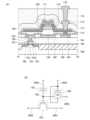
図1(A)は、トランジスタ100および容量素子130の上面図である。図1(B)は
、図1(A)にA1-A2の一点鎖線で示した部位の断面図である。図1(C)は、図1
(A)にB1-B2の一点鎖線で示した部位の断面図である。<A: Configuration Examples of Transistors and Capacitors>
1A is a top view of a
1A is a cross-sectional view of the portion indicated by the dashed dotted line B1-B2 in FIG.
図1に示すトランジスタ100は、基板101上に形成されている。また、トランジスタ
100は、電極102、絶縁層106、絶縁層107、酸化物半導体層108、電極10
9、電極119、絶縁層110、電極111、および絶縁層112を有する。また、図1
(A)および図1(B)では、電極103および電極104も図示している。The
9, an
1A and 1B, an
より具体的には、基板101上に電極102、電極103、電極104が形成され、それ
ぞれの電極の間に絶縁層105が形成されている。電極102は、電極102aの上に電
極102bを積層した構造を有する。電極103は、電極103aの上に電極103bを
積層した構造を有する。電極104は、電極104aの上に電極104bを積層した構造
を有する。絶縁層106は、電極102bの一部と、電極103bの一部と、電極104
bの一部に接して、絶縁層105上に形成されている。More specifically,
The insulating
また、絶縁層107は、電極102bの一部と、電極103bの一部と、電極104bの
一部に接して、絶縁層106上に形成されている。絶縁層107は凸部を有し、該凸部上
に酸化物半導体層108aと酸化物半導体層108bが形成されている。また、電極10
9および電極119は、酸化物半導体層108bに接して形成されている。電極119は
、絶縁層107に形成された開口を介して電極104と電気的に接続されている。The insulating
The insulating
また、酸化物半導体層108cは、酸化物半導体層108b、電極109、および電極1
19に接して形成されている。図1では、酸化物半導体層108a、酸化物半導体層10
8b、および酸化物半導体層108cを酸化物半導体層108と示している。The
In FIG. 1 , the
8b and the
また、酸化物半導体層108c上に絶縁層110が形成され、絶縁層110上に電極11
1が形成されている。また、電極109、電極119、電極111を覆って絶縁層112
が形成されている。In addition, an insulating
An insulating
is formed.
電極111は、ゲート電極として機能することができる。絶縁層110は、ゲート絶縁層
として機能することができる。電極109は、ソース電極またはドレイン電極の一方とし
て機能することができる。電極119は、ソース電極またはドレイン電極の他方として機
能することができる。電極102はバックゲート電極として機能することができる。トラ
ンジスタ100は、チャネルが形成される半導体層に酸化物半導体を用いたトランジスタ
である。トランジスタ100はトップゲート型のトランジスタの一種と考えることができ
る。The
ここで、バックゲート電極について説明しておく。一般に、バックゲート電極は導電層で
形成され、ゲート電極とバックゲート電極で半導体層のチャネル形成領域を挟むように配
置される。よって、バックゲート電極は、ゲート電極と同様に機能させることができる。
バックゲート電極の電位は、ゲート電極と同電位としてもよいし、GND電位や、任意の
電位としてもよい。また、バックゲート電極の電位をゲート電極と連動させず独立して変
化させることで、トランジスタのしきい値電圧を変化させることができる。Here, the back gate electrode will be explained. In general, the back gate electrode is formed of a conductive layer and is arranged so that the gate electrode and the back gate electrode sandwich the channel formation region of the semiconductor layer. Therefore, the back gate electrode can be made to function in the same way as the gate electrode.
The potential of the back gate electrode may be the same as that of the gate electrode, may be GND potential, or may be any potential. In addition, the threshold voltage of the transistor can be changed by changing the potential of the back gate electrode independently of the gate electrode.
トランジスタ100が有する電極111および電極102は、どちらもゲート電極として
機能することができる。よって、絶縁層110および絶縁層107は、どちらもゲート絶
縁層として機能することができる。よって、電極111および電極102のどちらか一方
を、単に「ゲート電極」という場合、他方を「バックゲート電極」という。また、電極1
11および電極102のどちらか一方を、「第1のゲート電極」といい、他方を「第2の
ゲート電極」という場合がある。また、電極102を「ゲート電極」として用いる場合は
、トランジスタ100をボトムゲート型のトランジスタの一種と考えることができる。Both the
One of the electrode 11 and the
酸化物半導体層108を挟んで電極111および電極102を設けることで、更には、電
極111および電極102を同電位とすることで、酸化物半導体層108においてキャリ
アの流れる領域が膜厚方向においてより大きくなるため、キャリアの移動量が増加する。
この結果、トランジスタ100のオン電流が大きくなる共に、電界効果移動度が高くなる
。By providing the
As a result, the on-state current of the
したがって、トランジスタ100は、占有面積に対して大きいオン電流を有するトランジ
スタである。すなわち、求められるオン電流に対して、トランジスタ100の占有面積を
小さくすることができる。本発明の一態様によれば、トランジスタの占有面積を小さくす
ることができる。よって、本発明の一態様によれば、集積度の高い半導体装置を実現する
ことができる。Therefore, the
また、ゲート電極とバックゲート電極は導電層で形成されるため、トランジスタの外部で
生じる電界が、チャネルが形成される半導体層に作用しないようにする機能(特に静電気
に対する静電遮蔽機能)を有する。In addition, since the gate electrode and the back gate electrode are formed of a conductive layer, they have a function of preventing an electric field generated outside the transistor from acting on the semiconductor layer in which the channel is formed (especially, an electrostatic shielding function against static electricity).
また、電極111および電極102は、それぞれが外部からの電界を遮蔽する機能を有す
るため、基板101側や、電極111側に設けられる荷電粒子等の電荷が酸化物半導体層
108に影響しない。この結果、ストレス試験(例えば、ゲートに負の電荷を印加する-
GBT(Gate Bias-Temperature)ストレス試験)の劣化が抑制さ
れると共に、異なるドレイン電圧におけるオン電流の立ち上がり電圧の変動を抑制するこ
とができる。なお、この効果は、電極111および電極102が、同電位、または異なる
電位の場合において生じる。In addition, since the
This can suppress deterioration in a GBT (Gate Bias-Temperature) stress test, and can also suppress fluctuations in the on-state current rise voltage at different drain voltages. This effect occurs whether the
なお、BTストレス試験は加速試験の一種であり、長期間の使用によって起こるトランジ
スタの特性変化(すなわち、経年変化)を、短時間で評価することができる。特に、BT
ストレス試験前後におけるトランジスタのしきい値電圧の変動量は、信頼性を調べるため
の重要な指標となる。BTストレス試験前後において、しきい値電圧の変動量が少ないほ
ど、信頼性が高いトランジスタであるといえる。The BT stress test is a type of accelerated test, and can evaluate, in a short period of time, the changes in transistor characteristics (i.e., aging) that occur during long-term use.
The amount of change in threshold voltage of a transistor before and after a stress test is an important index for examining reliability. The smaller the amount of change in threshold voltage before and after a BT stress test, the more reliable the transistor is.
また、電極111および電極102を有し、且つ電極111および電極102を同電位と
することで、BTストレス試験前後におけるしきい値電圧の変動量が低減される。このた
め、複数のトランジスタにおける電気特性のばらつきも同時に低減される。In addition, by providing the
また、バックゲート電極を有するトランジスタ100は、ゲートに正の電荷を印加する+
GBTストレス試験前後におけるしきい値電圧の変動が小さい。In addition, the
The variation in threshold voltage before and after the GBT stress test is small.
また、バックゲート電極側から光が入射する場合に、バックゲート電極を、遮光性を有す
る導電膜で形成することで、バックゲート電極側から半導体層に光が入射することを防ぐ
ことができる。よって、半導体層の光劣化を防ぎ、トランジスタのしきい値電圧がシフト
するなどの電気特性の劣化を防ぐことができる。In addition, when light is incident from the back gate electrode side, the back gate electrode can be formed of a conductive film having a light blocking property to prevent the light from being incident on the semiconductor layer from the back gate electrode side, thereby preventing photodegradation of the semiconductor layer and deterioration of electrical characteristics such as a shift in the threshold voltage of the transistor.
続いて、「しきい値電圧」について説明しておく。ここでは、電極111をゲート電極と
して用いる。電極111に電圧が印加されると、該電圧に応じた強さの電界が、絶縁層1
10を介して酸化物半導体層108に印加され、酸化物半導体層108中にキャリアが生
じ、チャネルが形成される。チャネルが形成されると、電極109と電極119が電気的
に接続されて導通状態(オン状態)となる。酸化物半導体層108中にチャネルが形成さ
れはじめる時の電極111の電圧を、「しきい値電圧」という。Next, the "threshold voltage" will be explained. Here, the
A voltage is applied to the
例えば、トランジスタ100がnチャネル型のトランジスタで、電極109をソース電極
、電極119をドレイン電極として用いる場合、電極109の電位を0Vとした時に、電
極111にしきい値電圧以上の電圧が印加されると、電極109から酸化物半導体層10
8中にキャリアが供給されて、チャネルが形成される。なお、一般に、半導体層中のチャ
ネルが形成される領域を、「チャネル形成領域」という。この時、電極119に正の電圧
が印加されると、電極109から電極119に向かってキャリアが流れる。換言すると、
電極119から電極109に向かって電流が流れる。なお、トランジスタがオン状態の時
のソース電極とドレイン電極間に流れる電流を「オン電流」という。また、トランジスタ
がオフ状態の時のソース電極とドレイン電極間に流れる電流を「オフ電流」という。For example, in the case where the
Carriers are supplied into
A current flows from the
絶縁層106、絶縁層112は、水素、水、アルカリ金属、アルカリ土類金属等の不純物
や、酸素が透過しにくい絶縁性材料を用いて形成することが好ましい。このような材料を
用いて絶縁層106、絶縁層112を形成することにより、外部から酸化物半導体層10
8への不純物の拡散を抑制することができる。また、酸化物半導体層108に含まれる酸
素が、外部へ拡散することを抑制することができる。The insulating
In addition, it is possible to suppress diffusion of impurities into the
また、電極102上の少なくとも一部には、絶縁層106を設けないことが好ましい。電
極102上の少なくとも一部に絶縁層106を設けないことで、電極102と酸化物半導
体層108の距離を、絶縁層106の厚さ分短くすることができる。よって、電極102
が酸化物半導体層108に及ぼす電界強度を高めることができる。よって、電極102の
、ゲート電極またはバックゲート電極としての機能を高めることができる。It is preferable that the insulating
The electric field strength acting on the
また、容量素子130は、電極103と電極109の間に、誘電体として絶縁層107を
挟んで形成されている。なお、本実施の形態では、電極103上の絶縁層106を除去し
ているが、電極103上の絶縁層106を除去せずに、絶縁層106と絶縁層107の積
層を誘電体として用いてもよい。The
また、トランジスタ100の外側で、絶縁層106と絶縁層112を接することが好まし
い。図1(B)では、図1(B)の両端部に絶縁層106と絶縁層112が接する領域が
示されている。このような構成とすることで、外部から酸化物半導体層108への不純物
の拡散を抑制する効果をより高めることができる。また、酸化物半導体層108に含まれ
る酸素が、外部へ拡散することを抑制する効果をより高めることができる。本発明の一態
様によれば、信頼性の良好な半導体装置を提供することができる。Moreover, the insulating
〔A-1:基板101〕
基板101として用いる材料に大きな制限はないが、少なくとも後の加熱処理に耐えうる
程度の耐熱性を有していることが必要となる。例えばバリウムホウケイ酸ガラスやアルミ
ノホウケイ酸ガラスなどのガラス基板、セラミック基板、石英基板、サファイア基板など
を用いることができる。[A-1: Substrate 101]
There is no particular limitation on the material used for the
また、基板101としてシリコンや炭化シリコンなどからなる単結晶半導体基板、多結晶
半導体基板、シリコンゲルマニウムなどからなる化合物半導体基板等を用いてもよい。ま
た、SOI基板や、半導体基板上に歪トランジスタやFIN型トランジスタなどの半導体
素子が設けられたものなどを用いることもできる。または、高電子移動度トランジスタ(
HEMT:High Electron Mobility Transistor)に
適用可能なヒ化ガリウム、ヒ化アルミニウムガリウム、ヒ化インジウムガリウム、窒化ガ
リウム、リン化インジウム、シリコンゲルマニウムなどを用いてもよい。これらの半導体
を用いることで、高速動作をすることに適したトランジスタとすることができる。すなわ
ち、基板101は、単なる支持基板に限らず、他のトランジスタなどのデバイスが形成さ
れた基板であってもよい。この場合、トランジスタ100のゲート電極、ソース電極、又
はドレイン電極の少なくとも一つは、上記他のデバイスと電気的に接続されていてもよい
。The
Gallium arsenide, aluminum gallium arsenide, indium gallium arsenide, gallium nitride, indium phosphide, silicon germanium, or the like that can be applied to a high electron mobility transistor (HEMT) may be used. By using these semiconductors, a transistor suitable for high-speed operation can be obtained. That is, the
なお、基板101として、可撓性基板(フレキシブル基板)を用いてもよい。可撓性基板
を用いる場合、可撓性基板上に、トランジスタや容量素子などを直接作製してもよいし、
他の作製基板上にトランジスタや容量素子などを作製し、その後可撓性基板に剥離、転置
してもよい。なお、作製基板から可撓性基板に剥離、転置するために、作製基板とトラン
ジスタや容量素子などとの間に、剥離層を設けるとよい。Note that a flexible substrate may be used as the
A transistor, a capacitor, or the like may be manufactured over another manufacturing substrate, and then peeled off and transferred to the flexible substrate. Note that in order to peel off and transfer from the manufacturing substrate to the flexible substrate, a peeling layer may be provided between the manufacturing substrate and the transistor, the capacitor, or the like.
〔A-2:電極102a、電極103a、および電極104a〕
電極102a、電極103a、および電極104aを形成するための導電性材料としては
、アルミニウム、クロム、銅、銀、金、白金、タンタル、ニッケル、チタン、モリブデン
、タングステン、ハフニウム(Hf)、バナジウム(V)、ニオブ(Nb)、マンガン、
マグネシウム、ジルコニウム、ベリリウム等から選ばれた金属元素、上述した金属元素を
成分とする合金、または上述した金属元素を組み合わせた合金などを用いることができる
。また、リン等の不純物元素を含有させた多結晶シリコンに代表される、電気伝導度が高
い半導体、ニッケルシリサイドなどのシリサイドを用いてもよい。導電層の形成方法は特
に限定されず、蒸着法、CVD法、スパッタリング法、スピンコート法などの各種形成方
法を用いることができる。[A-2: electrode 102a, electrode 103a, and
Examples of conductive materials for forming the
A metal element selected from magnesium, zirconium, beryllium, etc., an alloy containing the above-mentioned metal element, or an alloy combining the above-mentioned metal elements can be used. Also, a semiconductor with high electrical conductivity, typified by polycrystalline silicon containing an impurity element such as phosphorus, or a silicide such as nickel silicide can be used. The method for forming the conductive layer is not particularly limited, and various forming methods such as a vapor deposition method, a CVD method, a sputtering method, and a spin coating method can be used.
なお、一般に、CVD法は、プラズマを利用するプラズマCVD(PECVD:Plas
ma Enhanced CVD)法、熱を利用する熱CVD(TCVD:Therma
l CVD)法などに分類できる。さらに用いる原料ガスによって金属CVD(MCVD
:Metal CVD)法、有機金属CVD(MOCVD:Metal Organic
CVD)法などに分類できる。Generally, the CVD method is a plasma enhanced chemical vapor deposition (PECVD) method that uses plasma.
Enhanced CVD (TCVD) method, and Thermal CVD (Therma Enhanced CVD) method.
Furthermore, depending on the source gas used, it can be classified into metal CVD (MCVD) and
:Metal CVD) method, Metal Organic CVD (MOCVD) method
These methods include chemical vapor deposition (CVD) methods.
また、一般に、蒸着法は、抵抗加熱蒸着法、電子線蒸着法、MBE(Molecular
Beam Epitaxy)法、PLD(Pulsed Laser Deposit
ion)法、IAD蒸着(IAD:Ion beam Assisted Deposi
tion)法、ALD(ALD:Atomic Layer Deposition)法
などに分類できる。Generally, the deposition method includes resistance heating deposition, electron beam deposition, MBE (Molecular Beam Evaporation), etc.
Beam Epitaxy) method, PLD (Pulsed Laser Deposit)
ion) method, IAD: Ion beam Assisted Deposit
These methods can be classified into an atomic layer deposition (ALD) method, an atomic layer deposition (ALD) method, and the like.
プラズマCVD法は、比較的低温で高品質の膜が得られる。MOCVD法や蒸着法などの
、成膜時にプラズマを用いない成膜方法を用いると、被形成面にダメージが生じにくく、
また、欠陥の少ない膜が得られる。The plasma CVD method can produce high-quality films at relatively low temperatures. When using a deposition method that does not use plasma during deposition, such as MOCVD or vapor deposition, damage to the deposition surface is less likely to occur.
Furthermore, a film with fewer defects can be obtained.
また、電極102a、電極103a、および電極104aに、インジウム錫酸化物、酸化
タングステンを含むインジウム酸化物、酸化タングステンを含むインジウム亜鉛酸化物、
酸化チタンを含むインジウム酸化物、酸化チタンを含むインジウム錫酸化物、インジウム
亜鉛酸化物、シリコンを添加したインジウム錫酸化物などの酸素を含む導電性材料、窒化
チタン、窒化タンタルなどの窒素を含む導電性材料を適用することもできる。また、前述
した金属元素を含む材料と、酸素を含む導電性材料を組み合わせた積層構造とすることも
できる。また、前述した金属元素を含む材料と、窒素を含む導電性材料を組み合わせた積
層構造とすることもできる。また、前述した金属元素を含む材料、酸素を含む導電性材料
、および窒素を含む導電性材料を組み合わせた積層構造とすることもできる。In addition, the
Conductive materials containing oxygen, such as indium oxide containing titanium oxide, indium tin oxide containing titanium oxide, indium zinc oxide, and indium tin oxide doped with silicon, and conductive materials containing nitrogen, such as titanium nitride and tantalum nitride, can also be applied. A laminate structure can also be formed by combining the above-mentioned material containing a metal element with a conductive material containing oxygen. A laminate structure can also be formed by combining the above-mentioned material containing a metal element with a conductive material containing nitrogen. A laminate structure can also be formed by combining the above-mentioned material containing a metal element, a conductive material containing oxygen, and a conductive material containing nitrogen.
電極102a、電極103a、および電極104aは、単層構造でも、二層以上の積層構
造としてもよい。例えば、シリコンを含むアルミニウム層の単層構造、アルミニウム層上
にチタン層を積層する二層構造、窒化チタン層上にチタン層を積層する二層構造、窒化チ
タン層上にタングステン層を積層する二層構造、窒化タンタル層上にタングステン層を積
層する二層構造、チタン層と、そのチタン層上にアルミニウム層を積層し、さらにその上
にチタン層を形成する三層構造などがある。また、アルミニウムに、チタン、タンタル、
タングステン、モリブデン、クロム、ネオジム、スカンジウムから選ばれた元素の層、ま
たは複数組み合わせた合金層、もしくは窒化物層を用いてもよい。The
A layer of an element selected from tungsten, molybdenum, chromium, neodymium, and scandium, or an alloy layer of a combination of a plurality of elements, or a nitride layer may be used.
電極102a、電極103a、および電極104aの厚さは、10nm以上500nm以
下、好ましくは50nm以上300nm以下とすればよい。The thickness of the
〔A-3:電極102b、電極103b、および電極104b〕
電極102b、電極103b、および電極104bは、水素、水、アルカリ金属、アルカ
リ土類金属等の不純物や酸素が透過しにくい導電性材料を用いて形成することが好ましい
。このような導電性材料としては、インジウム錫酸化物、シリコン、リン、ボロン、窒素
、および/または炭素を含むインジウム錫酸化物、シリコン、リン、ボロン、窒素、およ
び/または炭素を含むインジウムガリウム亜鉛酸化物、などの導電性酸化物材料を挙げる
ことができる。また、窒化タンタル、ルテニウムなどの導電性材料を挙げることができる
。また、電極102b、電極103b、および電極104bは、単層構造でも、二層以上
の積層構造としてもよい。[A-3:
The
電極102b、電極103b、および電極104bの厚さは、10nm以上500nm以
下、好ましくは50nm以上300nm以下とすればよい。The thickness of the
また、電極102a、電極103a、および電極104aを設けずに、電極102、電極
103、および電極104を、電極102b、電極103b、および電極104bのみで
構成してもよい。Furthermore, the
〔A-4:絶縁層105〕
絶縁層105は、窒化アルミニウム、酸化アルミニウム、窒化酸化アルミニウム、酸化窒
化アルミニウム、酸化マグネシウム、窒化シリコン、酸化シリコン、窒化酸化シリコン、
酸化窒化シリコン、酸化ガリウム、酸化ゲルマニウム、酸化イットリウム、酸化ジルコニ
ウム、酸化ランタン、酸化ネオジム、酸化ハフニウム、酸化タンタルから選ばれた材料を
、単層でまたは積層して形成することができる。また、酸化物材料、窒化物材料、酸化窒
化物材料、窒化酸化物材料のうち、複数の材料を混合した材料を用いてもよい。[A-4: Insulating layer 105]
The insulating
The insulating layer 10 may be formed of a single layer or a multilayer of a material selected from the group consisting of silicon oxynitride, gallium oxide, germanium oxide, yttrium oxide, zirconium oxide, lanthanum oxide, neodymium oxide, hafnium oxide, and tantalum oxide. Alternatively, a mixture of a plurality of oxide materials, nitride materials, oxynitride materials, and nitride oxide materials may be used.
なお、本明細書中において、窒化酸化物とは、酸素よりも窒素の含有量が多い化合物をい
う。また、酸化窒化物とは、窒素よりも酸素の含有量が多い化合物をいう。なお、各元素
の含有量は、例えば、ラザフォード後方散乱法(RBS:Rutherford Bac
kscattering Spectrometry)等を用いて測定することができる
。In this specification, the term "nitride oxide" refers to a compound containing more nitrogen than oxygen. The term "oxynitride" refers to a compound containing more oxygen than nitrogen. The content of each element can be measured, for example, by Rutherford Backscattering Spectroscopy (RBS).
The measurement can be performed using a spectrometer such as a scattering spectrometry (STEM).
絶縁層105を複数層の積層とする場合は、例えば、1層目を窒化シリコン層とし、2層
目を酸化シリコン層としてもよい。この場合、酸化シリコン層は酸化窒化シリコン層でも
構わない。また、窒化シリコン層は窒化酸化シリコン層でも構わない。When the insulating
絶縁層105の厚さは、10nm以上500nm以下、好ましくは50nm以上300n
m以下とすればよい。The thickness of the insulating
m or less.
〔A-5:絶縁層106〕
絶縁層106は、水素、水、アルカリ金属、アルカリ土類金属等の不純物や酸素が透過し
にくい絶縁性材料を用いて形成することが好ましい。このような絶縁性材料としては、酸
化アルミニウム、窒化アルミニウム、酸化窒化アルミニウム、窒化酸化アルミニウム、酸
化ガリウム、酸化ゲルマニウム、酸化イットリウム、酸化ジルコニウム、酸化ランタン、
酸化ネオジム、酸化ハフニウム、酸化タンタルなどの絶縁性酸化物材料を挙げることがで
きる。[A-5: Insulating layer 106]
The insulating
Examples of the insulating oxide material include neodymium oxide, hafnium oxide, and tantalum oxide.
絶縁層106の厚さは、10nm以上500nm以下、好ましくは50nm以上300n
m以下とすればよい。The thickness of the insulating
m or less.
〔A-6:絶縁層107〕
絶縁層107は、絶縁層105と同様の材料および方法で形成することができる。また、
酸化物半導体中の水素濃度の増加を防ぐために、絶縁層107の水素濃度を低減すること
が好ましい。具体的には、絶縁層107の水素濃度を、SIMSにおいて、2×10²⁰
atoms/cm3以下、好ましくは5×1019atoms/cm3以下、より好まし
くは1×10¹⁹atoms/cm3以下、さらに好ましくは5×1018atoms/
cm3以下とする。また、酸化物半導体中の窒素濃度の増加を防ぐために、絶縁層107
の窒素濃度を低減することが好ましい。具体的には、絶縁層107の窒素濃度を、SIM
Sにおいて、5×10¹⁹atoms/cm3未満、好ましくは5×1018atoms
/cm3以下、より好ましくは1×1018atoms/cm3以下、さらに好ましくは
5×10¹⁷atoms/cm3以下とする。[A-6: Insulating layer 107]
The insulating
In order to prevent an increase in the hydrogen concentration in the oxide semiconductor, it is preferable to reduce the hydrogen concentration in the insulating
atoms/cm3 or less, preferably 5×10¹⁹ atoms/cm3 or less, more preferably 1×10¹⁹ atoms/cm3 or less, and even more preferably 5×10¹⁸ atoms/
In order to preventan increase in the nitrogen concentration in the oxide semiconductor,
Specifically, it is preferable to reduce the nitrogen concentration in the insulating
S is less than 5×10¹⁹ atoms/cm3 , preferably less than 5×10¹⁸ atoms
/cm3 or less, more preferably 1×10¹⁸ atoms/cm3 or less, and further preferably 5×10¹⁷ atoms/cm3 or less.
また、絶縁層107は、化学量論的組成を満たす酸素よりも多くの酸素を含む絶縁層を用
いて形成することが好ましい。化学量論的組成を満たす酸素よりも多くの酸素を含む絶縁
層は、加熱により酸素の一部が脱離する。化学量論的組成を満たす酸素よりも多くの酸素
を含む絶縁層は、TDS分析にて、酸素原子に換算しての酸素の脱離量が1.0×101
8atoms/cm3以上、好ましくは3.0×1020atoms/cm3以上である
絶縁層である。なお、上記TDS分析時における膜の表面温度としては100℃以上70
0℃以下、または100℃以上500℃以下の範囲が好ましい。The insulating
The insulating layer has a density of 3.0×10²⁰ atoms/cm3 or more, preferably 3.0×10²⁰ atoms/cm3 or more. The surface temperature of the film during the TDS analysis is 100° C. or more and 70° C. or less.
A temperature range of 0° C. or lower, or 100° C. to 500° C. is preferred.
絶縁層106の厚さは、10nm以上500nm以下、好ましくは50nm以上300n
m以下とすればよい。The thickness of the insulating
m or less.
〔A-7:酸化物半導体層108〕
酸化物半導体層108は、酸化物半導体層108a、酸化物半導体層108b、酸化物半
導体層108cを積層した構成を有する。[A-7: Oxide semiconductor layer 108]
The
酸化物半導体層108a、酸化物半導体層108b、および酸化物半導体層108cは、
インジウムもしくはガリウムの一方、または両方を含む材料で形成する。代表的には、I
n-Ga酸化物(InとGaを含む酸化物)、In-Zn酸化物(InとZnを含む酸化
物)、In-M-Zn酸化物(Inと、元素Mと、Znを含む酸化物。)がある。The
It is formed of a material containing either indium or gallium, or both.
Examples of such oxides include n-Ga oxide (oxide containing In and Ga), In-Zn oxide (oxide containing In and Zn), and In-M-Zn oxide (oxide containing In, element M, and Zn).
元素Mは、好ましくは、アルミニウム、ガリウム、イットリウムまたはスズなどとする。
そのほかの元素Mに適用可能な元素としては、ホウ素、シリコン、チタン、鉄、ニッケル
、ゲルマニウム、イットリウム、ジルコニウム、モリブデン、ランタン、セリウム、ネオ
ジム、ハフニウム、タンタル、タングステンなどがある。ただし、元素Mとして、前述の
元素を複数組み合わせても構わない場合がある。元素Mは、例えば、酸素との結合エネル
ギーが高い元素である。元素Mは、例えば、酸化物のエネルギーギャップを大きくする機
能を有する元素である。酸化物半導体層108は、元素Mを含む酸化物半導体であること
が好ましい。また、酸化物半導体は、亜鉛を含むと好ましい。酸化物が亜鉛を含むと、例
えば、酸化物を結晶化しやすくなる。The element M is preferably aluminum, gallium, yttrium, tin or the like.
Other elements applicable to the element M include boron, silicon, titanium, iron, nickel, germanium, yttrium, zirconium, molybdenum, lanthanum, cerium, neodymium, hafnium, tantalum, and tungsten. However, the element M may be a combination of a plurality of the above elements. The element M is, for example, an element having a high bond energy with oxygen. The element M is, for example, an element having a function of increasing the energy gap of an oxide. The
ただし、酸化物半導体は、インジウムを含む酸化物に限定されない。酸化物半導体は、例
えば、亜鉛スズ酸化物、ガリウムスズ酸化物であっても構わない。However, the oxide semiconductor is not limited to an oxide containing indium, and may be, for example, zinc tin oxide or gallium tin oxide.
酸化物半導体層108は、スパッタリング法、CVD(Chemical Vapor
Deposition)法(MOCVD(Metal Organic Chemica
l Vapor Deposition)法、ALD(Atomic Layer De
position)法、熱CVD法またはPECVD(Plasma Enhanced
Chemical Vapor Deposition)法を含むがこれに限定されな
い)、MBE(Molecular Beam Epitaxy)法またはPLD(Pu
lsed Laser Deposition)法を用いて成膜するとよい。特に、MO
CVD法、ALD法または熱CVD法を用いると、プラズマを使わないため酸化物半導体
層108にダメージを与えにくく、トランジスタのオフ状態のリーク電流を低く抑えるこ
とができるので好ましい。The
Deposition method (MOCVD (Metal Organic Chemical
l Vapor Deposition) method, ALD (Atomic Layer Deposition) method,
position method, thermal CVD method or PECVD (Plasma Enhanced
Chemical Vapor Deposition (MBE), Molecular Beam Epitaxy (PMEA), or PLD (Pu
It is preferable to form the film by using the LSLD method.
The CVD method, the ALD method, or the thermal CVD method is preferable because no plasma is used and therefore the
例えば、酸化物半導体層108として、熱CVD法でInGaZnOX(X>0)膜を成
膜する場合には、トリメチルインジウム、トリメチルガリウム、及びジメチル亜鉛を用い
る。なお、トリメチルインジウムの化学式は、In(CH3)3である。また、トリメチ
ルガリウムの化学式は、Ga(CH3)3である。また、ジメチル亜鉛の化学式は、Zn
(CH3)2である。また、これらの組み合わせに限定されず、トリメチルガリウムに代
えてトリエチルガリウム(化学式Ga(C2H5)3)を用いることもでき、ジメチル亜
鉛に代えてジエチル亜鉛(化学式Zn(C2H5)2)を用いることもできる。For example, in the case where an InGaZnOx (X>0) film is formed as the
(CH3 )2. In addition, the combination is not limited to these, and triethylgallium (chemical formula: Ga(C2 H5 )3 ) can be used instead of trimethylgallium, and diethylzinc (chemical formula: Zn(C2 H5 )2 ) can be used instead of dimethylzinc.
例えば、酸化物半導体層108として、ALD法で、InGaZnOX(X>0)膜を成
膜する場合には、In(CH3)3ガスとO3ガスを順次繰り返し導入してInO2層を
形成し、その後、Ga(CH3)3ガスとO3ガスを同時に導入してGaO層を形成し、
更にその後Zn(CH3)2とO3ガスを同時に導入してZnO層を形成する。なお、こ
れらの層の順番はこの例に限らない。また、これらのガスを混ぜてInGaO2層やIn
ZnO2層、GaInO層、ZnInO層、GaZnO層などの混合化合物層を形成して
も良い。なお、O3ガスに変えてAr等の不活性ガスでバブリングしたH2Oガスを用い
ても良いが、Hを含まないO3ガスを用いる方が好ましい。また、In(CH3)3ガス
にかえて、In(C2H5)3ガスやトリス(アセチルアセトナト)インジウムを用いて
も良い。なお、トリス(アセチルアセトナト)インジウムは、In(acac)3とも呼
ぶ。また、Ga(CH3)3ガスにかえて、Ga(C2H5)3ガスやトリス(アセチル
アセトナト)ガリウムを用いても良い。なお、トリス(アセチルアセトナト)ガリウムは
、Ga(acac)3とも呼ぶ。また、In(CH3)3ガスにかえて、In(C2H5
)3ガスを用いても良い。また、Zn(CH3)2ガスや、酢酸亜鉛を用いても良い。こ
れらのガス種には限定されない。For example, when anInGaZnOx (X>0) film is formed as the
Then, Zn(CH3 )2 and O3 gases are introduced at the same time to form a ZnO layer. The order of these layers is not limited to this example. In addition, these gases can be mixed to form an InGaO2 layer or an In
A mixed compound layer such as aZnO2 layer, a GaInO layer, a ZnInO layer, or a GaZnO layer may be formed. Note that, instead ofO3 gas,H2O gas bubbled with an inert gas such as Ar may be used, but it is preferable to useO3 gas that does not contain H. Also, instead of In(CH3 )3 gas, In(C2H5 )3 gas or tris(acetylacetonato)indium may be used. Note that tris(acetylacetonato)indium is also called In(acac)3 . Also, instead of Ga(CH3)3 gas, Ga(C2H5 )3 gas or tris(acetylacetonato)gallium may be used. Notethat tris(acetylacetonato)gallium is also called Ga(acac)3. Also, instead of In(CH3 )3 gas, In(C2H5 )3 gas or tris(acetylacetonato)gallium may be used. Note that tris(acetylacetonato)gallium is also called Ga(acac)3 . Also, instead of In(CH3 )3 gas, In(C2H5 )3 gas or tris(acetylacetonato )gallium may be used.
Alternatively, Zn(CH3 )2 gas or zinc acetate may be used. The gas species is not limitedto these.
酸化物半導体層108をスパッタリング法で成膜する場合、パーティクル数低減のため、
インジウムを含むターゲットを用いると好ましい。また、元素Mの原子数比が高い酸化物
ターゲットを用いた場合、ターゲットの導電性が低くなる場合がある。インジウムを含む
ターゲットを用いる場合、ターゲットの導電率を高めることができ、DC放電、AC放電
が容易となるため、大面積の基板へ対応しやすくなる。したがって、半導体装置の生産性
を高めることができる。In the case where the
It is preferable to use a target containing indium. In addition, when an oxide target having a high atomic ratio of element M is used, the conductivity of the target may be reduced. When a target containing indium is used, the conductivity of the target can be increased, and DC discharge and AC discharge become easier, making it easier to handle large-area substrates. Therefore, the productivity of semiconductor devices can be improved.
酸化物半導体層108をスパッタリング法で成膜する場合、ターゲットの原子数比は、I
n:M:Znが3:1:1、3:1:2、3:1:4、1:1:0.5、1:1:1、1
:1:2、1:4:4、などとすればよい。In the case where the
n:M:Zn is 3:1:1, 3:1:2, 3:1:4, 1:1:0.5, 1:1:1, 1
:1:2, 1:4:4, etc.
酸化物半導体層108をスパッタリング法で成膜する場合、ターゲットの原子数比からず
れた原子数比の膜が形成される場合がある。特に、亜鉛は、ターゲットの原子数比よりも
膜の原子数比が小さくなる場合がある。具体的には、ターゲットに含まれる亜鉛の原子数
比の40atomic%以上90atomic%程度以下となる場合がある。When the
酸化物半導体層108aおよび酸化物半導体層108cは、酸化物半導体層108bを構
成する金属元素のうち、1種類以上の同じ金属元素を含む材料により形成されることが好
ましい。このような材料を用いると、酸化物半導体層108aおよび酸化物半導体層10
8bとの界面、ならびに酸化物半導体層108cおよび酸化物半導体層108bとの界面
に界面準位を生じにくくすることができる。よって、界面におけるキャリアの散乱や捕獲
が生じにくく、トランジスタの電界効果移動度を向上させることが可能となる。また、ト
ランジスタのしきい値電圧のばらつきを低減することが可能となる。よって、良好な電気
特性を有する半導体装置を実現することが可能となる。The
It is possible to prevent interface states from being generated at the interface with the oxide semiconductor layer 8b and the interface with the
酸化物半導体層108aおよび酸化物半導体層108cの厚さは、3nm以上100nm
以下、好ましくは3nm以上50nm以下とする。また、酸化物半導体層108bの厚さ
は、3nm以上200nm以下、好ましくは3nm以上100nm以下、さらに好ましく
は3nm以上50nm以下とする。The
The thickness of the
また、酸化物半導体層108bがIn-M-Zn酸化物であり、酸化物半導体層108a
および酸化物半導体層108cもIn-M-Zn酸化物であるとき、酸化物半導体層10
8aおよび酸化物半導体層108cをIn:M:Zn=x1:y1:z1[原子数比]、
酸化物半導体層108bをIn:M:Zn=x2:y2:z2[原子数比]とすると、y
1/x1がy2/x2よりも大きくなる酸化物半導体層108a、酸化物半導体層108
c、および酸化物半導体層108bを選択する。好ましくは、y1/x1がy2/x2よ
りも1.5倍以上大きくなる酸化物半導体層108a、酸化物半導体層108c、および
酸化物半導体層108bを選択する。さらに好ましくは、y1/x1がy2/x2よりも
2倍以上大きくなる酸化物半導体層108a、酸化物半導体層108c、および酸化物半
導体層108bを選択する。より好ましくは、y1/x1がy2/x2よりも3倍以上大
きくなる酸化物半導体層108a、酸化物半導体層108cおよび酸化物半導体層108
bを選択する。このとき、酸化物半導体層108bにおいて、y1がx1以上であるとト
ランジスタに安定した電気特性を付与できるため好ましい。ただし、y1がx1の3倍以
上になると、トランジスタの電界効果移動度が低下してしまうため、y1はx1の3倍未
満であると好ましい。酸化物半導体層108aおよび酸化物半導体層108cを上記構成
とすることにより、酸化物半導体層108aおよび酸化物半導体層108cを、酸化物半
導体層108bよりも酸素欠損が生じにくい層とすることができる。The
When the
The oxide semiconductor layer 8a and the
When the
The
Preferably, the
b is selected. In this case, in the
なお、酸化物半導体層108aおよび酸化物半導体層108cがIn-M-Zn酸化物で
あり、InおよびMの和を100atomic%としたときのInとMの原子数比率は好
ましくはInが50atomic%未満、Mが50atomic%以上、さらに好ましく
はInが25atomic%未満、Mが75atomic%以上とする。また、酸化物半
導体層108bがIn-M-Zn酸化物であり、InおよびMの和を100atomic
%としたときのInとMの原子数比率は好ましくはInが25atomic%以上、Mが
75atomic%未満、さらに好ましくはInが34atomic%以上、Mが66a
tomic%未満とする。Note that the
%, the atomic ratio of In and M is preferably 25 atomic % or more of In and less than 75 atomic %, and more preferably 34 atomic % or more of In and less than 66 atomic % of M.
The percentage must be less than tomic percent.
例えば、InまたはGaを含む酸化物半導体層108a、およびInまたはGaを含む酸
化物半導体層108cとしてIn:Ga:Zn=1:3:2、1:3:4、1:3:6、
1:6:4、または1:9:6などの原子数比のターゲットを用いて形成したIn-Ga
-Zn酸化物や、In:Ga=1:9、または7:93などの原子数比のターゲットを用
いて形成したIn-Ga酸化物を用いることができる。また、酸化物半導体層108bと
して、例えば、In:Ga:Zn=1:1:1または3:1:2などの原子数比のターゲ
ットを用いて形成したIn-Ga-Zn酸化物を用いることができる。なお、酸化物半導
体層108a、酸化物半導体層108bおよび酸化物半導体層108cの原子数比はそれ
ぞれ、誤差として上記の原子数比のプラスマイナス20%の変動を含む。For example, the
In-Ga formed using targets with atomic ratios of 1:6:4 or 1:9:6
For example, an In—Ga oxide formed using a target having an atomic ratio of In:Ga=1:9 or 7:93 can be used as the
酸化物半導体層108を用いたトランジスタに安定した電気特性を付与するためには、特
に酸化物半導体層108中の不純物及び酸素欠損を低減して高純度真性化し、酸化物半導
体層108を真性または実質的に真性と見なせる酸化物半導体層とすることが好ましい。
また、少なくとも酸化物半導体層108中のチャネル形成領域が真性または実質的に真性
と見なせる半導体層とすることが好ましい。In order to give stable electrical characteristics to a transistor including the
At least a channel formation region in the
なお、実質的に真性と見なせる酸化物半導体層とは、酸化物半導体層中のキャリア密度が
、1×10¹⁷/cm3未満、1×1015/cm3未満、または1×1013/cm3
未満である酸化物半導体層をいう。Note that an oxide semiconductor layer that can be regarded as substantially intrinsic is an oxide semiconductor layer having a carrier density of less than 1×10¹⁷ /cm3 , less than 1×10¹⁵ /cm3 , or less than 1×10¹³ /cm3 .
The term "oxide semiconductor layer" refers to an oxide semiconductor layer having a thickness of less than 100 nm.
ここで、酸化物半導体層108a、酸化物半導体層108b、および酸化物半導体層10
8cの積層により構成される酸化物半導体層108の機能およびその効果について、図6
に示すエネルギーバンド構造図を用いて説明する。図6は、図1(C)にC1-C2の一
点鎖線で示した部位のエネルギーバンド構造を示している。また、図6は、トランジスタ
100のチャネル形成領域のエネルギーバンド構造を示している。Here, the
The function and effect of the
6 shows the energy band structure of the portion indicated by the dashed line C1-C2 in FIG. 1C. Also, FIG. 6 shows the energy band structure of the channel formation region of the
図6中、Ec382、Ec383a、Ec383b、Ec383c、Ec386は、それ
ぞれ、絶縁層107、酸化物半導体層108a、酸化物半導体層108b、酸化物半導体
層108c、絶縁層110の伝導帯下端のエネルギーを示している。In FIG. 6, Ec382, Ec383a, Ec383b, Ec383c, and Ec386 represent the energies of the conduction band minimums of the insulating
ここで、真空準位と伝導帯下端のエネルギーとの差(「電子親和力」ともいう。)は、真
空準位と価電子帯上端のエネルギーとの差(イオン化ポテンシャルともいう。)からエネ
ルギーギャップを引いた値となる。なお、エネルギーギャップは、分光エリプソメータ(
HORIBA JOBIN YVON社 UT-300)を用いて測定できる。また、真
空準位と価電子帯上端のエネルギー差は、紫外線光電子分光分析(UPS:Ultrav
iolet Photoelectron Spectroscopy)装置(PHI社
VersaProbe)を用いて測定できる。Here, the difference between the vacuum level and the energy at the bottom of the conduction band (also called "electron affinity") is the difference between the vacuum level and the energy at the top of the valence band (also called "ionization potential") minus the energy gap. The energy gap is measured using a spectroscopic ellipsometer (
The energy difference between the vacuum level and the top of the valence band can be measured using ultraviolet photoelectron spectroscopy (UPS: Ultraviolet
The measurement can be performed using a iontophoretic photoelectron spectroscopy (VersaProbe, manufactured by PHI).
なお、原子数比がIn:Ga:Zn=1:3:2のターゲットを用いて形成したIn-G
a-Zn酸化物のエネルギーギャップは約3.5eV、電子親和力は約4.5eVである
。また、原子数比がIn:Ga:Zn=1:3:4のターゲットを用いて形成したIn-
Ga-Zn酸化物のエネルギーギャップは約3.4eV、電子親和力は約4.5eVであ
る。また、原子数比がIn:Ga:Zn=1:3:6のターゲットを用いて形成したIn
-Ga-Zn酸化物のエネルギーギャップは約3.3eV、電子親和力は約4.5eVで
ある。また、原子数比がIn:Ga:Zn=1:6:2のターゲットを用いて形成したI
n-Ga-Zn酸化物のエネルギーギャップは約3.9eV、電子親和力は約4.3eV
である。また、原子数比がIn:Ga:Zn=1:6:8のターゲットを用いて形成した
In-Ga-Zn酸化物のエネルギーギャップは約3.5eV、電子親和力は約4.4e
Vである。また、原子数比がIn:Ga:Zn=1:6:10のターゲットを用いて形成
したIn-Ga-Zn酸化物のエネルギーギャップは約3.5eV、電子親和力は約4.
5eVである。また、原子数比がIn:Ga:Zn=1:1:1のターゲットを用いて形
成したIn-Ga-Zn酸化物のエネルギーギャップは約3.2eV、電子親和力は約4
.7eVである。また、原子数比がIn:Ga:Zn=3:1:2のターゲットを用いて
形成したIn-Ga-Zn酸化物のエネルギーギャップは約2.8eV、電子親和力は約
5.0eVである。The In-Ga alloy was formed using a target with an atomic ratio of In:Ga:Zn=1:3:2.
The energy gap of a-Zn oxide is about 3.5 eV, and the electron affinity is about 4.5 eV. In-
The energy gap of Ga-Zn oxide is about 3.4 eV, and the electron affinity is about 4.5 eV. In was formed using a target with an atomic ratio of In:Ga:Zn=1:3:6.
The energy gap of the In-Ga-Zn oxide is about 3.3 eV, and the electron affinity is about 4.5 eV. In addition, the In-Ga-Zn oxide was formed using a target with an atomic ratio of In:Ga:Zn=1:6:2.
The energy gap of n-Ga-Zn oxide is about 3.9 eV, and the electron affinity is about 4.3 eV.
The energy gap of the In-Ga-Zn oxide formed using a target with an atomic ratio of In:Ga:Zn=1:6:8 is about 3.5 eV, and the electron affinity is about 4.4 e
V. The energy gap of an In-Ga-Zn oxide formed using a target with an atomic ratio of In:Ga:Zn=1:6:10 is about 3.5 eV, and the electron affinity is about 4.
The energy gap of an In-Ga-Zn oxide formed using a target with an atomic ratio of In:Ga:Zn=1:1:1 is about 3.2 eV, and the electron affinity is about 4.
The energy gap of an In-Ga-Zn oxide formed using a target with an atomic ratio of In:Ga:Zn=3:1:2 is about 2.8 eV, and the electron affinity is about 5.0 eV.
絶縁層107と絶縁層110は絶縁物であるため、Ec382とEc386は、Ec38
3a、Ec383b、およびEc383cよりも真空準位に近い(電子親和力が小さい)
。Since the insulating
Closer to the vacuum level (lower electron affinity) than 3a, Ec383b, and Ec383c
.
また、Ec383aは、Ec383bよりも真空準位に近い。具体的には、Ec383a
は、Ec383bよりも0.05eV以上、0.07eV以上、0.1eV以上または0
.15eV以上、かつ2eV以下、1eV以下、0.5eV以下または0.4eV以下真
空準位に近いことが好ましい。Also, Ec383a is closer to the vacuum level than Ec383b.
is 0.05 eV or more, 0.07 eV or more, 0.1 eV or more, or 0
It is preferable that the energy level is 15 eV or more and 2 eV or less, 1 eV or less, 0.5 eV or less, or 0.4 eV or less, which is close to the vacuum level.
また、Ec383cは、Ec383bよりも真空準位に近い。具体的には、Ec383c
は、Ec383bよりも0.05eV以上、0.07eV以上、0.1eV以上または0
.15eV以上、かつ2eV以下、1eV以下、0.5eV以下または0.4eV以下真
空準位に近いことが好ましい。Also, Ec383c is closer to the vacuum level than Ec383b.
is 0.05 eV or more, 0.07 eV or more, 0.1 eV or more, or 0
It is preferable that the energy level is 15 eV or more and 2 eV or less, 1 eV or less, 0.5 eV or less, or 0.4 eV or less, which is close to the vacuum level.
また、酸化物半導体層108aと酸化物半導体層108bとの界面近傍、および、酸化物
半導体層108bと酸化物半導体層108cとの界面近傍では、混合領域が形成されるた
め、伝導帯下端のエネルギーは連続的に変化する。即ち、これらの界面において、準位は
存在しないか、ほとんどない。In addition, near the interface between the
従って、当該エネルギーバンド構造を有する積層構造において、電子は酸化物半導体層1
08bを主として移動することになる。そのため、酸化物半導体層108aと絶縁層10
7との界面、または、酸化物半導体層108cと絶縁層110との界面に準位が存在した
としても、当該準位は電子の移動にほとんど影響しない。また、酸化物半導体層108a
と酸化物半導体層108bとの界面、および酸化物半導体層108cと酸化物半導体層1
08bとの界面に準位が存在しないか、ほとんどないため、当該領域において電子の移動
を阻害することもない。従って、上記酸化物半導体の積層構造を有するトランジスタ10
0は、高い電界効果移動度を実現することができる。Therefore, in the stacked structure having the above energy band structure, electrons are
Therefore, the
Even if a state exists at the interface between the
and the interface between the
Since there is no or almost no level at the interface with 08b, the movement of electrons in the region is not hindered.
0 can achieve high field effect mobility.
なお、図6に示すように、酸化物半導体層108aと絶縁層107の界面、および酸化物
半導体層108cと絶縁層110の界面近傍には、不純物や欠陥に起因したトラップ準位
390が形成され得るものの、酸化物半導体層108a、および酸化物半導体層108c
があることにより、酸化物半導体層108bと当該トラップ準位とを遠ざけることができ
る。As shown in FIG. 6 , trap states 390 due to impurities or defects may be formed near the interface between the
This can keep the
特に、本実施の形態に例示するトランジスタ100は、チャネル幅方向において、酸化物
半導体層108bの上面と側面が酸化物半導体層108cと接し、酸化物半導体層108
bの下面が酸化物半導体層108aと接して形成されている(図1(C)参照。)。この
ように、酸化物半導体層108bを酸化物半導体層108aと酸化物半導体層108cで
覆う構成とすることで、上記トラップ準位の影響をさらに低減することができる。In particular, in the
The bottom surface of the
ただし、Ec383aまたはEc383cと、Ec383bとのエネルギー差が小さい場
合、酸化物半導体層108bの電子が該エネルギー差を越えてトラップ準位に達すること
がある。トラップ準位に電子が捕獲されることで、絶縁層の界面にマイナスの固定電荷が
生じ、トランジスタのしきい値電圧はプラス方向にシフトしてしまう。However, when the energy difference between Ec383a or Ec383c and Ec383b is small, electrons in the
従って、Ec383a、およびEc383cと、Ec383bとのエネルギー差を、それ
ぞれ0.1eV以上、好ましくは0.15eV以上とすると、トランジスタのしきい値電
圧の変動が低減され、トランジスタの電気特性を良好なものとすることができるため、好
ましい。Therefore, it is preferable that the energy difference between Ec383a and Ec383c and between Ec383b and Ec383b is 0.1 eV or more, and preferably 0.15 eV or more, because the fluctuation in the threshold voltage of the transistor can be reduced and the electrical characteristics of the transistor can be favorable.
また、酸化物半導体層108a、および酸化物半導体層108cのバンドギャップは、酸
化物半導体層108bのバンドギャップよりも広いほうが好ましい。The band gaps of the
[酸化物半導体について]
以下では、酸化物半導体層108に適用可能な酸化物半導体について詳細に説明する。[Oxide Semiconductors]
An oxide semiconductor that can be used for the
酸化物半導体層108a、酸化物半導体層108b、酸化物半導体層108cに適用可能
な酸化物半導体は、インジウムを含む酸化物である。酸化物は、例えば、インジウムを含
むと、キャリア移動度(電子移動度)が高くなる。An oxide semiconductor that can be used for the
ただし、酸化物半導体は、インジウムを含む酸化物に限定されない。酸化物半導体は、例
えば、亜鉛スズ酸化物、ガリウムスズ酸化物であっても構わない。However, the oxide semiconductor is not limited to an oxide containing indium, and may be, for example, zinc tin oxide or gallium tin oxide.
また酸化物半導体は、エネルギーギャップが大きい酸化物を用いる。酸化物半導体のエネ
ルギーギャップは、例えば、2.5eV以上4.2eV以下、好ましくは2.8eV以上
3.8eV以下、さらに好ましくは3eV以上3.5eV以下とする。The oxide semiconductor used has a large energy gap, for example, from 2.5 eV to 4.2 eV, preferably from 2.8 eV to 3.8 eV, more preferably from 3 eV to 3.5 eV.
以下では、酸化物半導体中における不純物の影響について説明する。なお、トランジスタ
の電気特性を安定にするためには、酸化物半導体中の不純物濃度を低減し、低キャリア密
度化および高純度化することが有効である。なお、酸化物半導体のキャリア密度は、1×
1017個/cm3未満、1×1015個/cm3未満、または1×1013個/cm3
未満とする。酸化物半導体中の不純物濃度を低減するためには、近接する膜中の不純物濃
度も低減することが好ましい。The influence of impurities in an oxide semiconductor will be described below. Note that in order to stabilize the electrical characteristics of a transistor, it is effective to reduce the impurity concentration in the oxide semiconductor to reduce the carrier density and to increase the purity. Note that the carrier density of an oxide semiconductor is 1×
Less than 1017 particles/cm3 , less than 1×10¹⁵ particles/cm3 , or 1×10¹³ particles/cm3
In order to reduce the impurity concentration in the oxide semiconductor, it is preferable to also reduce the impurity concentration in a nearby film.
例えば、酸化物半導体中のシリコンは、キャリアトラップやキャリア発生源となる場合が
ある。そのため、酸化物半導体と絶縁層107および絶縁層110との間におけるシリコ
ン濃度を、二次イオン質量分析法(SIMS:Secondary Ion Mass
Spectrometry)において、1×10¹⁹atoms/cm3未満、好ましく
は5×10¹⁸atoms/cm3未満、さらに好ましくは2×1018atoms/c
m3未満とする。For example, silicon in an oxide semiconductor may become a carrier trap or a carrier generation source. Therefore, the silicon concentration between the oxide semiconductor and the insulating
Spectrometry) is less than 1×10¹⁹ atoms/cm3 , preferably less than 5×10¹⁸ atoms/cm3 , and more preferably less than 2×10¹⁸ atoms/
Less than3 m.
以下では、酸化物半導体の構造について説明する。The structure of oxide semiconductors is explained below.
酸化物半導体は、例えば、非単結晶酸化物半導体と単結晶酸化物半導体とに分けられる。
または、酸化物半導体は、例えば、結晶性酸化物半導体と非晶質酸化物半導体とに分けら
れる。非単結晶酸化物半導体とは、CAAC-OS(C Axis Aligned C
rystalline Oxide Semiconductor)、多結晶酸化物半導
体、微結晶酸化物半導体、非晶質酸化物半導体などがある。また、結晶性酸化物半導体と
しては、単結晶酸化物半導体、CAAC-OS、多結晶酸化物半導体、微結晶酸化物半導
体などがある。Oxide semiconductors are classified into, for example, non-single-crystal oxide semiconductors and single-crystal oxide semiconductors.
Alternatively, oxide semiconductors can be classified into, for example, crystalline oxide semiconductors and amorphous oxide semiconductors.
Examples of crystalline oxide semiconductors include single-crystal oxide semiconductors, CAAC-OS, polycrystalline oxide semiconductors, microcrystalline oxide semiconductors, and amorphous oxide semiconductors. Examples of crystalline oxide semiconductors include single-crystal oxide semiconductors, CAAC-OS, polycrystalline oxide semiconductors, and microcrystalline oxide semiconductors.
《CAAC-OS》
まずは、CAAC-OSについて説明する。《CAAC-OS》
First, the CAAC-OS will be described.
CAAC-OSは、c軸配向した複数の結晶部(ペレットともいう。)を有する酸化物半
導体の一つである。CAAC-OS is a type of oxide semiconductor that has a plurality of crystal parts (also referred to as pellets) that are c-axis aligned.
透過型電子顕微鏡(TEM:Transmission Electron Micro
scope)によって、CAAC-OSの明視野像および回折パターンの複合解析像(高
分解能TEM像ともいう。)を観察することで複数のペレットを確認することができる。
一方、高分解能TEM像によっても明確なペレット同士の境界、即ち結晶粒界(グレイン
バウンダリーともいう。)を確認することができない。そのため、CAAC-OSは、結
晶粒界に起因する電子移動度の低下が起こりにくいといえる。Transmission Electron Microscope (TEM)
A bright-field image and a composite analysis image of a diffraction pattern of the CAAC-OS (also referred to as a high-resolution TEM image) can be observed using a high-resolution TEM (transmission electron microscope) to confirm multiple pellets.
On the other hand, a clear boundary between pellets, that is, a crystal grain boundary, cannot be confirmed even in a high-resolution TEM image. Therefore, it can be said that a decrease in electron mobility due to a crystal grain boundary is unlikely to occur in the CAAC-OS.
例えば、図7(A)に示すように、試料面と略平行な方向から、CAAC-OSの断面の
高分解能TEM像を観察する。ここでは、球面収差補正(Spherical Aber
ration Corrector)機能を用いてTEM像を観察する。なお、球面収差
補正機能を用いた高分解能TEM像を、以下では、特にCs補正高分解能TEM像と呼ぶ
。なお、Cs補正高分解能TEM像の取得は、例えば、日本電子株式会社製原子分解能分
析電子顕微鏡JEM-ARM200Fなどによって行うことができる。For example, as shown in FIG. 7A, a high-resolution TEM image of a cross section of CAAC-OS is observed from a direction substantially parallel to the sample surface.
The TEM image is observed using a spherical aberration corrector function. Hereinafter, a high-resolution TEM image using the spherical aberration correction function is particularly referred to as a Cs-corrected high-resolution TEM image. The Cs-corrected high-resolution TEM image can be obtained, for example, using an atomic resolution analytical electron microscope JEM-ARM200F manufactured by JEOL Ltd.
図7(A)の領域(1)を拡大したCs補正高分解能TEM像を図7(B)に示す。図7
(B)より、ペレットにおいて、金属原子が層状に配列していることを確認できる。金属
原子の各層は、CAAC-OSの膜を形成する面(被形成面ともいう。)または上面の凹
凸を反映した形状であり、CAAC-OSの被形成面または上面と平行に配列する。FIG. 7B shows an enlarged Cs-corrected high-resolution TEM image of region (1) in FIG. 7A.
From FIG. 1B, it can be seen that metal atoms are arranged in layers in the pellet, and each layer of metal atoms has a shape reflecting the unevenness of the surface (also referred to as the surface on which the CAAC-OS film is formed) or the top surface, and is arranged in parallel to the surface on which the CAAC-OS film is formed or the top surface.
図7(B)において、CAAC-OSは特徴的な原子配列を有する。図7(C)は、特徴
的な原子配列を、補助線で示したものである。図7(B)および図7(C)より、ペレッ
ト一つの大きさは1nm以上3nm以下程度であり、ペレットとペレットとの傾きにより
生じる隙間の大きさは0.8nm程度であることがわかる。したがって、ペレットを、ナ
ノ結晶(nc:nanocrystal)と呼ぶこともできる。In Fig. 7B, the CAAC-OS has a characteristic atomic arrangement. Fig. 7C shows the characteristic atomic arrangement with auxiliary lines. Fig. 7B and Fig. 7C show that the size of each pellet is about 1 nm to 3 nm, and the size of the gap caused by the inclination between the pellets is about 0.8 nm. Therefore, the pellets can also be called nanocrystals (nc).
ここで、Cs補正高分解能TEM像から、基板5120上のCAAC-OSのペレット5
100の配置を模式的に示すと、レンガまたはブロックが積み重なったような構造となる
(図7(D)参照。)。図7(C)で観察されたペレットとペレットとの間で傾きが生じ
ている箇所は、図7(D)に示す領域5161に相当する。Here, from the Cs-corrected high-resolution TEM image, the
A schematic diagram of the arrangement of 100 is a structure like stacked bricks or blocks (see FIG. 7(D)). The portion where the pellets are tilted as observed in FIG. 7(C) corresponds to the region 5161 shown in FIG. 7(D).
また、例えば、図8(A)に示すように、試料面と略垂直な方向から、CAAC-OSの
平面のCs補正高分解能TEM像を観察する。図8(A)の領域(1)、領域(2)およ
び領域(3)を拡大したCs補正高分解能TEM像を、それぞれ図8(B)、図8(C)
および図8(D)に示す。図8(B)、図8(C)および図8(D)より、ペレットは、
金属原子が三角形状、四角形状または六角形状に配列していることを確認できる。しかし
ながら、異なるペレット間で、金属原子の配列に規則性は見られない。For example, as shown in FIG. 8A, a Cs-corrected high-resolution TEM image of a plane of CAAC-OS is observed from a direction substantially perpendicular to the sample surface. Enlarged Cs-corrected high-resolution TEM images of regions (1), (2), and (3) in FIG. 8A are shown in FIG. 8B and FIG. 8C, respectively.
8(B), 8(C) and 8(D). From FIG. 8(B), FIG. 8(C) and FIG. 8(D), the pellet is
It can be seen that the metal atoms are arranged in triangular, tetragonal or hexagonal shapes, but there is no regularity in the arrangement of the metal atoms between different pellets.
例えば、InGaZnO4の結晶を有するCAAC-OSに対し、X線回折(XRD:X
-Ray Diffraction)装置を用いてout-of-plane法による構
造解析を行うと、図9(A)に示すように回折角(2θ)が31°近傍にピークが現れる
場合がある。このピークは、InGaZnO4の結晶の(009)面に帰属されることか
ら、CAAC-OSの結晶がc軸配向性を有し、c軸が被形成面または上面に略垂直な方
向を向いていることが確認できる。For example, X-ray diffraction (XRD) was performed on CAAC-OS having InGaZnO crystals.
When a structural analysis is performed by an out-of-plane method using a Diffraction (Frequency-Ray Diffraction) apparatus, a peak may appear at a diffraction angle (2θ) of about 31°, as shown in Fig. 9A. This peak is attributed to the (009) plane of the InGaZnO4 crystal, and it can be confirmed that the CAAC-OS crystal has c-axis orientation, and the c-axis faces in a direction approximately perpendicular to the surface on which the CAAC-OS is formed or the upper surface.
なお、InGaZnO4の結晶を有するCAAC-OSのout-of-plane法に
よる構造解析では、2θが31°近傍のピークの他に、2θが36°近傍にもピークが現
れる場合がある。2θが36°近傍のピークは、CAAC-OS中の一部に、c軸配向性
を有さない結晶が含まれることを示している。CAAC-OSは、2θが31°近傍にピ
ークを示し、2θが36°近傍にピークを示さないことが好ましい。In addition, in a structural analysis of CAAC-OS havingInGaZnO4 crystals by an out-of-plane method, in addition to a peak at 2θ of about 31°, a peak at 2θ of about 36° may also appear. The peak at 2θ of about 36° indicates that a part of the CAAC-OS contains crystals that do not have c-axis orientation. It is preferable that the CAAC-OS shows a peak at 2θ of about 31° and does not show a peak at 2θ of about 36°.
一方、CAAC-OSに対し、c軸に略垂直な方向からX線を入射させるin-plan
e法による構造解析を行うと、2θが56°近傍にピークが現れる。このピークは、In
GaZnO4の結晶の(110)面に帰属される。CAAC-OSの場合は、2θを56
°近傍に固定し、試料面の法線ベクトルを軸(φ軸)として試料を回転させながら分析(
φスキャン)を行っても、図9(B)に示すように明瞭なピークは現れない。これに対し
、InGaZnO4の単結晶酸化物半導体であれば、2θを56°近傍に固定してφスキ
ャンした場合、図9(C)に示すように(110)面と等価な結晶面に帰属されるピーク
が6本観察される。したがって、XRDを用いた構造解析から、CAAC-OSは、a軸
およびb軸の配向が不規則であることが確認できる。On the other hand, in-plan X-ray irradiation is performed on CAAC-OS from a direction substantially perpendicular to the c-axis.
When the structure is analyzed by the .DELTA. method, a peak appears at 2.theta. of about 56 degrees. This peak is due to In
This is attributed to the (110) plane of the GaZnO4 crystal. In the case of CAAC-OS, 2θ is set to 56
The sample was rotated around the normal vector of the sample surface as the axis (φ axis) while performing the analysis (
9B, no clear peak appears. In contrast, in the case of a single-crystal oxide semiconductor of InGaZnO4 , when φ scanning is performed with 2θ fixed at approximately 56°, six peaks attributable to a crystal plane equivalent to the (110) plane are observed as shown in FIG 9C. Therefore, the structure analysis using XRD confirms that the orientation of the a-axis and b-axis of the CAAC-OS is irregular.
次に、CAAC-OSであるIn-Ga-Zn酸化物に対し、試料面に平行な方向からプ
ローブ径が300nmの電子線を入射させたときの回折パターン(制限視野透過電子回折
パターンともいう。)を図10(A)に示す。図10(A)より、例えば、InGaZn
O4の結晶の(009)面に起因するスポットが確認される。したがって、電子回折によ
っても、CAAC-OSに含まれるペレットがc軸配向性を有し、c軸が被形成面または
上面に略垂直な方向を向いていることがわかる。一方、同じ試料に対し、試料面に垂直な
方向からプローブ径が300nmの電子線を入射させたときの回折パターンを図10(B
)に示す。図10(B)より、リング状の回折パターンが確認される。したがって、電子
回折によっても、CAAC-OSに含まれるペレットのa軸およびb軸は配向性を有さな
いことがわかる。なお、図10(B)における第1リングは、InGaZnO4の結晶の
(010)面および(100)面などに起因すると考えられる。また、図10(B)にお
ける第2リングは(110)面などに起因すると考えられる。Next, a diffraction pattern (also referred to as a selected area transmission electron diffraction pattern) obtained when an electron beam with a probe diameter of 300 nm is incident on an In—Ga—Zn oxide, which is a CAAC-OS, in a direction parallel to the sample surface is shown in FIG.
A spot due to the (009) plane of theO4 crystal is confirmed. Therefore, it is found by electron diffraction that the pellets contained in the CAAC-OS have c-axis orientation, and the c-axis faces a direction approximately perpendicular to the surface on which the sample is formed or the top surface. On the other hand, the diffraction pattern when an electron beam with a probe diameter of 300 nm is incident on the same sample from a direction perpendicular to the sample surface is shown in FIG. 10 (B).
) is shown in FIG. 10B. A ring-shaped diffraction pattern is observed. Therefore, it is found by electron diffraction that the a-axis and b-axis of the pellets contained in CAAC-OS do not have any orientation. The first ring in FIG. 10B is considered to be caused by the (010) and (100) planes of the InGaZnO4 crystal. The second ring in FIG. 10B is considered to be caused by the (110) plane.
このように、それぞれのペレット(ナノ結晶)のc軸が、被形成面または上面に略垂直な
方向を向いていることから、CAAC-OSをCANC(C-Axis Aligned
nanocrystals)を有する酸化物半導体と呼ぶこともできる。In this way, the c-axis of each pellet (nanocrystal) is oriented in a direction substantially perpendicular to the surface on which the nanocrystal is formed or the upper surface. Therefore, the CAAC-OS is called C-Axis Aligned (CANC).
The oxide semiconductor having nanocrystals may also be referred to as an oxide semiconductor having nanocrystals.
CAAC-OSは、不純物濃度の低い酸化物半導体である。不純物は、水素、炭素、シリ
コン、遷移金属元素などの酸化物半導体の主成分以外の元素である。特に、シリコンなど
の、酸化物半導体を構成する金属元素よりも酸素との結合力の強い元素は、酸化物半導体
から酸素を奪うことで酸化物半導体の原子配列を乱し、結晶性を低下させる要因となる。
また、鉄やニッケルなどの重金属、アルゴン、二酸化炭素などは、原子半径(または分子
半径)が大きいため、酸化物半導体内部に含まれると、酸化物半導体の原子配列を乱し、
結晶性を低下させる要因となる。なお、酸化物半導体に含まれる不純物は、キャリアトラ
ップやキャリア発生源となる場合がある。CAAC-OS is an oxide semiconductor with a low concentration of impurities. The impurities are elements other than the main components of the oxide semiconductor, such as hydrogen, carbon, silicon, and transition metal elements. In particular, elements such as silicon that bond stronger to oxygen than metal elements constituting the oxide semiconductor remove oxygen from the oxide semiconductor, thereby disturbing the atomic arrangement of the oxide semiconductor and causing a decrease in crystallinity.
In addition, heavy metals such as iron and nickel, argon, and carbon dioxide have large atomic (or molecular) radii, so when they are contained inside an oxide semiconductor, they disrupt the atomic arrangement of the oxide semiconductor,
Impurities contained in an oxide semiconductor may function as a carrier trap or a carrier generation source.
また、CAAC-OSは、欠陥準位密度の低い酸化物半導体である。例えば、酸化物半導
体中の酸素欠損は、キャリアトラップとなることや、水素を捕獲することによってキャリ
ア発生源となることがある。In addition, the CAAC-OS is an oxide semiconductor with a low density of defect states. For example, oxygen vacancies in an oxide semiconductor can serve as carrier traps or as a carrier generation source by capturing hydrogen.
また、CAAC-OSを用いたトランジスタは、可視光や紫外光の照射による電気特性の
変動が小さい。Furthermore, in a transistor using CAAC-OS, change in electrical characteristics due to irradiation with visible light or ultraviolet light is small.
《微結晶酸化物半導体》
次に、微結晶酸化物半導体について説明する。<<Microcrystalline oxide semiconductor>>
Next, a microcrystalline oxide semiconductor will be described.
微結晶酸化物半導体は、高分解能TEM像において、結晶部を確認することのできる領域
と、明確な結晶部を確認することのできない領域と、を有する。微結晶酸化物半導体に含
まれる結晶部は、1nm以上100nm以下、または1nm以上10nm以下の大きさで
あることが多い。特に、1nm以上10nm以下、または1nm以上3nm以下の微結晶
であるナノ結晶を有する酸化物半導体を、nc-OS(nanocrystalline
Oxide Semiconductor)と呼ぶ。また、nc-OSは、例えば、高
分解能TEM像では、結晶粒界を明確に確認できない場合がある。なお、ナノ結晶は、C
AAC-OSにおけるペレットと同じ起源を有する可能性がある。そのため、以下ではn
c-OSの結晶部をペレットと呼ぶ場合がある。A microcrystalline oxide semiconductor has regions where crystal parts can be confirmed in a high-resolution TEM image and regions where no clear crystal parts can be confirmed. The crystal parts contained in a microcrystalline oxide semiconductor often have a size of 1 nm to 100 nm, or 1 nm to 10 nm. In particular, an oxide semiconductor having nanocrystals that are microcrystals with a size of 1 nm to 10 nm, or 1 nm to 3 nm, is called nc-OS (nanocrystalline oxide semiconductor).
In the nc-OS, the crystal grain boundaries may not be clearly observed in a high-resolution TEM image.
It is possible that the origin of the pellets is the same as that of the pellets in AAC-OS.
The crystal parts of c-OS are sometimes called pellets.
nc-OSは、微小な領域(例えば、1nm以上10nm以下の領域、特に1nm以上3
nm以下の領域)において原子配列に周期性を有する。また、nc-OSは、異なるペレ
ット間で結晶方位に規則性が見られない。そのため、膜全体で配向性が見られない。した
がって、nc-OSは、分析方法によっては、非晶質酸化物半導体と区別が付かない場合
がある。例えば、nc-OSに対し、ペレットよりも大きい径のX線を用いるXRD装置
を用いて構造解析を行うと、out-of-plane法による解析では、結晶面を示す
ピークが検出されない。また、nc-OSは、ペレットよりも大きいプローブ径(例えば
、50nm以上)の電子線を用いる電子回折(制限視野電子回折ともいう。)を行うと、
ハローパターンのような回折パターンが観測される。一方、nc-OSに対し、ペレット
の大きさと近いか、ペレットより小さいプローブ径(例えば1nm以上30nm以下)の
電子線を用いる電子回折(以下、ナノビーム電子回折ともいう。)を行うと、スポットが
観測される。また、nc-OSに対しナノビーム電子回折を行うと、円を描くように(リ
ング状に)輝度の高い領域が観測される場合がある。また、nc-OSに対しナノビーム
電子回折を行うと、リング状の領域内に複数のスポットが観測される場合がある。The nc-OS is a microscopic region (for example, a region of 1 nm to 10 nm, particularly 1 nm to 3
The atomic arrangement has periodicity in the region of 0.1 nm or less. In addition, the nc-OS has no regularity in the crystal orientation between different pellets. Therefore, no orientation is observed throughout the film. Therefore, the nc-OS may be indistinguishable from an amorphous oxide semiconductor depending on the analysis method. For example, when a structural analysis is performed on the nc-OS using an XRD apparatus using X-rays with a diameter larger than that of the pellets, no peak indicating a crystal plane is detected in the out-of-plane analysis. In addition, when the nc-OS is subjected to electron diffraction (also referred to as selected area electron diffraction) using an electron beam with a probe diameter larger than that of the pellets (for example, 50 nm or more),
A diffraction pattern such as a halo pattern is observed. On the other hand, when electron diffraction (hereinafter also referred to as nanobeam electron diffraction) is performed on the nc-OS using an electron beam with a probe diameter (for example, 1 nm or more and 30 nm or less) close to the size of the pellet or smaller than the pellet, spots are observed. When nanobeam electron diffraction is performed on the nc-OS, a region with high brightness that draws a circle (ring shape) may be observed. When nanobeam electron diffraction is performed on the nc-OS, multiple spots may be observed within the ring-shaped region.
このように、それぞれのペレット(ナノ結晶)の結晶方位が規則性を有さないことから、
nc-OSをNANC(Non-Aligned nanocrystals)を有する
酸化物半導体と呼ぶこともできる。In this way, the crystal orientation of each pellet (nanocrystal) is not regular.
The nc-OS can also be referred to as an oxide semiconductor having non-aligned nanocrystals (NANC).
nc-OSは、非晶質酸化物半導体よりも規則性の高い酸化物半導体である。そのため、
nc-OSは、非晶質酸化物半導体よりも欠陥準位密度が低くなる。ただし、nc-OS
は、異なるペレット間で結晶方位に規則性が見られない。そのため、nc-OSは、CA
AC-OSと比べて欠陥準位密度が高くなる。The nc-OS is an oxide semiconductor that has higher order than an amorphous oxide semiconductor.
The nc-OS has a lower density of defect states than an amorphous oxide semiconductor.
In the case of nc-OS, there is no regularity in the crystal orientation between different pellets.
The density of defect states is higher than that of AC-OS.
《非晶質酸化物半導体》
次に、非晶質酸化物半導体について説明する。<Amorphous oxide semiconductor>
Next, the amorphous oxide semiconductor will be described.
非晶質酸化物半導体は、膜中における原子配列が不規則であり、結晶部を有さない酸化物
半導体である。石英のような無定形状態を有する酸化物半導体が一例である。An amorphous oxide semiconductor is an oxide semiconductor in which the atomic arrangement in the film is irregular and does not have crystal parts, such as an amorphous oxide semiconductor like quartz.
非晶質酸化物半導体は、高分解能TEM像において、結晶部を確認することができない。In amorphous oxide semiconductors, no crystalline parts can be seen in high-resolution TEM images.
非晶質酸化物半導体に対し、XRD装置を用いた構造解析を行うと、out-of-pl
ane法による解析では、結晶面を示すピークが検出されない。また、非晶質酸化物半導
体に対し、電子回折を行うと、ハローパターンが観測される。また、非晶質酸化物半導体
に対し、ナノビーム電子回折を行うと、スポットが観測されず、ハローパターンが観測さ
れる。When the structure of an amorphous oxide semiconductor is analyzed using an XRD device, out-of-phase
In the analysis by the AN method, no peaks indicating crystal planes are detected. In addition, when electron diffraction is performed on the amorphous oxide semiconductor, a halo pattern is observed. In addition, when nanobeam electron diffraction is performed on the amorphous oxide semiconductor, no spots are observed, but a halo pattern is observed.
非晶質構造については、様々な見解が示されている。例えば、原子配列に全く秩序性を有
さない構造を完全な非晶質構造(completely amorphous stru
cture)と呼ぶ場合がある。また、最近接原子間距離または第2近接原子間距離まで
秩序性を有し、かつ長距離秩序性を有さない構造を非晶質構造と呼ぶ場合もある。したが
って、最も厳格な定義によれば、僅かでも原子配列に秩序性を有する酸化物半導体を非晶
質酸化物半導体と呼ぶことはできない。また、少なくとも、長距離秩序性を有する酸化物
半導体を非晶質酸化物半導体と呼ぶことはできない。よって、結晶部を有することから、
例えば、CAAC-OSおよびnc-OSを、非晶質酸化物半導体または完全な非晶質酸
化物半導体と呼ぶことはできない。There are various views on the amorphous structure. For example, a structure that has no order in the atomic arrangement is called a completely amorphous structure.
In addition, a structure that has order up to the nearest interatomic distance or the second nearest interatomic distance and does not have long-range order is sometimes called an amorphous structure. Therefore, according to the strictest definition, an oxide semiconductor that has even a slight degree of order in its atomic arrangement cannot be called an amorphous oxide semiconductor. In addition, an oxide semiconductor that has at least long-range order cannot be called an amorphous oxide semiconductor. Therefore, since it has a crystalline part,
For example, the CAAC-OS and the nc-OS cannot be called an amorphous oxide semiconductor or a completely amorphous oxide semiconductor.
なお、酸化物半導体は、nc-OSと非晶質酸化物半導体との間の物性を示す構造を有す
る場合がある。そのような構造を有する酸化物半導体を、特に非晶質ライク酸化物半導体
(a-like OS:amorphous-like Oxide Semicond
uctor)と呼ぶ。Note that an oxide semiconductor may have a structure that exhibits physical properties between an nc-OS and an amorphous oxide semiconductor. An oxide semiconductor having such a structure is particularly referred to as an amorphous-like oxide semiconductor (a-like OS).
They are called "controllers."
a-like OSは、高分解能TEM像において鬆(ボイドともいう。)が観察される
場合がある。また、高分解能TEM像において、明確に結晶部を確認することのできる領
域と、結晶部を確認することのできない領域と、を有する。In the a-like OS, voids may be observed in a high-resolution TEM image, and the a-like OS has regions in which crystal parts can be clearly identified and regions in which crystal parts cannot be identified in the high-resolution TEM image.
以下では、酸化物半導体の構造による電子照射の影響の違いについて説明する。Below, we explain how the effects of electron irradiation differ depending on the structure of the oxide semiconductor.
a-like OS(試料A)、nc-OS(試料B)およびCAAC-OS(試料C)
を準備する。いずれの試料もIn-Ga-Zn酸化物である。a-like OS (sample A), nc-OS (sample B), and CAAC-OS (sample C)
All the samples are In--Ga--Zn oxides.
まず、各試料の高分解能断面TEM像を取得する。高分解能断面TEM像により、各試料
は、いずれも結晶部を有することがわかる。First, a high-resolution cross-sectional TEM image of each sample is obtained. The high-resolution cross-sectional TEM image shows that each sample has a crystalline portion.
さらに、各試料の結晶部の大きさを計測する。図11は、各試料の結晶部(22箇所から
45箇所)の平均の大きさの変化を調査した例である。図11より、a-like OS
は、電子の累積照射量に応じて結晶部が大きくなっていくことがわかる。具体的には、図
11中に(1)で示すように、TEMによる観察初期においては1.2nm程度の大きさ
だった結晶部(初期核ともいう。)が、累積照射量が4.2×10⁸e-/nm2におい
ては2.6nm程度の大きさまで成長していることがわかる。一方、nc-OSおよびC
AAC-OSは、電子照射開始時から電子の累積照射量が4.2×10⁸e-/nm2に
なるまでの範囲で、電子の累積照射量によらず結晶部の大きさに変化が見られないことが
わかる。具体的には、nc-OSは図11中の(2)で示すように、TEMによる観察の
経過によらず、結晶部の大きさは1.4nm程度であることがわかる。また、CAAC-
OSは図11中の(3)で示すように、TEMによる観察の経過によらず、結晶部の大き
さは2.1nm程度であることがわかる。Furthermore, the size of the crystal part of each sample is measured. Figure 11 shows an example of investigating the change in the average size of the crystal part (22 to 45 places) of each sample. From Figure 11, it can be seen that a-like OS
11, the crystal part grows in size according to the cumulative dose of electron irradiation. Specifically, as shown by (1) in FIG. 11, the crystal part (also called the initial nucleus) which was about 1.2 nm in size at the beginning of the TEM observation grows to about 2.6 nm in size when the cumulative dose of irradiation is 4.2×10⁸ e− /nm2 .
It can be seen that the size of the crystal parts of the AAC-OS does not change regardless of the cumulative electron irradiation dose from the start of electron irradiation until the cumulative electron irradiation dose reaches 4.2×10⁸ e− /nm2. Specifically, as shown by (2) in FIG. 11, the size of the crystal parts of the nc-OS is about 1.4 nm regardless of the course of TEM observation.
As shown by (3) in FIG. 11, the size of the crystal part of the OS is about 2.1 nm regardless of the course of TEM observation.
このように、a-like OSは、TEMによる観察程度の微量な電子照射によって、
結晶化が起こり、結晶部の成長が見られる場合がある。一方、良質なnc-OS、および
CAAC-OSであれば、TEMによる観察程度の微量な電子照射による結晶化はほとん
ど見られないことがわかる。In this way, the a-like OS can be observed by irradiating it with a small amount of electrons, which is equivalent to the amount observed by a TEM.
Crystallization may occur, and growth of crystal parts may be observed. On the other hand, in the case of high-quality nc-OS and CAAC-OS, crystallization due to a small amount of electron irradiation at the level observed by TEM is hardly observed.
なお、a-like OSおよびnc-OSの結晶部の大きさの計測は、高分解能TEM
像を用いて行うことができる。例えば、InGaZnO4の結晶は層状構造を有し、In
-O層の間に、Ga-Zn-O層を2層有する。InGaZnO4の結晶の単位格子は、
In-O層を3層有し、またGa-Zn-O層を6層有する、計9層がc軸方向に層状に
重なった構造を有する。よって、これらの近接する層同士の間隔は、(009)面の格子
面間隔(d値ともいう。)と同程度であり、結晶構造解析からその値は0.29nmと求
められている。そのため、高分解能TEM像における格子縞に着目し、格子縞の間隔が0
.28nm以上0.30nm以下である箇所においては、それぞれの格子縞がInGaZ
nO4の結晶のa-b面に対応する。The sizes of the crystal parts of the a-like OS and the nc-OS were measured using a high-resolution TEM.
For example, the crystal ofInGaZnO4 has a layered structure, and the In
The unit cell of the InGaZnO4 crystal is
It has a structure in which a total of nine layers, including three In-O layers and six Ga-Zn-O layers, are layered in the c-axis direction. Therefore, the distance between these adjacent layers is approximately the same as the lattice spacing (also called the d value) of the (009) plane, and the value is determined to be 0.29 nm from crystal structure analysis. Therefore, by focusing on the lattice fringes in the high-resolution TEM image, it was found that the spacing of the lattice fringes is 0.29 nm.
In the area where the width is 0.28 nm or more and 0.30 nm or less, the lattice fringes are InGaZ
It corresponds to the ab plane of thenO4 crystal.
また、酸化物半導体は、構造ごとに密度が異なる場合がある。例えば、ある酸化物半導体
の組成がわかれば、該組成と同じ組成における単結晶の密度と比較することにより、その
酸化物半導体の構造を推定することができる。例えば、単結晶の密度に対し、a-lik
e OSの密度は78.6%以上92.3%未満となる。また、例えば、単結晶の密度に
対し、nc-OSの密度およびCAAC-OSの密度は92.3%以上100%未満とな
る。なお、単結晶の密度に対し密度が78%未満となる酸化物半導体は、成膜すること自
体が困難である。In addition, the density of an oxide semiconductor may differ depending on the structure. For example, if the composition of an oxide semiconductor is known, the structure of the oxide semiconductor can be estimated by comparing the density of a single crystal having the same composition with the composition.
The density of the e-OS is 78.6% or more and less than 92.3%. For example, the density of the nc-OS and the CAAC-OS is 92.3% or more and less than 100% of the density of a single crystal. Note that it is difficult to deposit an oxide semiconductor having a density less than 78% of the density of a single crystal.
上記について、具体例を用いて説明する。例えば、In:Ga:Zn=1:1:1[原子
数比]を満たす酸化物半導体において、菱面体晶構造を有する単結晶InGaZnO4の
密度は6.357g/cm3となる。よって、例えば、In:Ga:Zn=1:1:1[
原子数比]を満たす酸化物半導体において、a-like OSの密度は5.0g/cm
3以上5.9g/cm3未満となる。また、例えば、In:Ga:Zn=1:1:1[原
子数比]を満たす酸化物半導体において、nc-OSの密度およびCAAC-OSの密度
は5.9g/cm3以上6.3g/cm3未満となる。The above will be described using a specific example. For example, in an oxide semiconductor that satisfies the atomic ratio of In:Ga:Zn=1:1:1, the density of single crystal InGaZnO4 having a rhombohedral crystal structure is 6.357 g/cm3 .
In the case of an oxide semiconductor that satisfies the above atomic ratio, the density of the a-like OS is 5.0 g/cm
In an oxide semiconductor having an atomic ratio of In:Ga:Zn=1:1:1, for example, the density of the nc-OS and the density of the CAAC-OS are 5.9 g/cm3or more and lessthan 6.3 g/cm3 .
なお、同じ組成の単結晶が存在しない場合がある。その場合、任意の割合で組成の異なる
単結晶を組み合わせることにより、所望の組成の単結晶に相当する密度を算出することが
できる。所望の組成の単結晶の密度は、組成の異なる単結晶を組み合わせる割合に対して
、加重平均を用いて算出すればよい。ただし、密度は、可能な限り少ない種類の単結晶を
組み合わせて算出することが好ましい。There may be cases where single crystals of the same composition do not exist. In such cases, the density corresponding to a single crystal of a desired composition can be calculated by combining single crystals of different compositions in any ratio. The density of a single crystal of a desired composition may be calculated using a weighted average of the ratio of the single crystals of different compositions combined. However, it is preferable to calculate the density by combining as few types of single crystals as possible.
なお、酸化物半導体は、例えば、非晶質酸化物半導体、a-like OS、微結晶酸化
物半導体、CAAC-OSのうち、二種以上を有する積層膜であってもよい。Note that the oxide semiconductor may be a stacked film including two or more of an amorphous oxide semiconductor, an a-like OS, a microcrystalline oxide semiconductor, and a CAAC-OS, for example.
不純物濃度が低く、欠陥準位密度が低い(酸素欠損が少ない)酸化物半導体は、キャリア
密度を低くすることができる。したがって、そのような酸化物半導体を、高純度真性また
は実質的に高純度真性な酸化物半導体と呼ぶ。CAAC-OSおよびnc-OSは、a-
like OSおよび非晶質酸化物半導体よりも不純物濃度が低く、欠陥準位密度が低い
。即ち、高純度真性または実質的に高純度真性な酸化物半導体となりやすい。したがって
、CAAC-OSまたはnc-OSを用いたトランジスタは、しきい値電圧がマイナスと
なる電気特性(ノーマリーオンともいう。)になることが少ない。また、高純度真性また
は実質的に高純度真性な酸化物半導体は、キャリアトラップが少ない。そのため、CAA
C-OSまたはnc-OSを用いたトランジスタは、電気特性の変動が小さく、信頼性の
高いトランジスタとなる。なお、酸化物半導体のキャリアトラップに捕獲された電荷は、
放出するまでに要する時間が長く、あたかも固定電荷のように振る舞うことがある。その
ため、不純物濃度が高く、欠陥準位密度が高い酸化物半導体を用いたトランジスタは、電
気特性が不安定となる場合がある。An oxide semiconductor having a low impurity concentration and a low density of defect states (few oxygen vacancies) can reduce the carrier density. Therefore, such an oxide semiconductor is called a high-purity intrinsic or substantially high-purity intrinsic oxide semiconductor.
The impurity concentration is lower and the density of defect states is lower than those of an amorphous oxide semiconductor and an amorphous oxide semiconductor. That is, the oxide semiconductor is likely to be a highly purified intrinsic or substantially highly purified intrinsic oxide semiconductor. Therefore, a transistor using a CAAC-OS or an nc-OS is unlikely to have electrical characteristics in which the threshold voltage is negative (also referred to as normally-on). In addition, a highly purified intrinsic or substantially highly purified intrinsic oxide semiconductor has fewer carrier traps.
A transistor using a C-OS or an nc-OS has little change in electrical characteristics and is highly reliable.
Since it takes a long time for the charge to be released, the charge may behave as if it is a fixed charge. Therefore, a transistor including an oxide semiconductor having a high impurity concentration and a high density of defect states may have unstable electrical characteristics.
<成膜モデル>
以下では、CAAC-OSおよびnc-OSの成膜モデルの一例について説明する。<Film formation model>
An example of a film formation model of the CAAC-OS and the nc-OS will be described below.
図12(A)は、スパッタリング法によりCAAC-OSが成膜される様子を示した成膜
室内の模式図である。FIG. 12A is a schematic diagram of the inside of a film formation chamber, illustrating how a CAAC-OS film is formed by a sputtering method.
ターゲット5130は、バッキングプレートに接着されている。バッキングプレートを介
してターゲット5130と向かい合う位置には、複数のマグネットが配置される。該複数
のマグネットによって磁場が生じている。マグネットの磁場を利用して成膜速度を高める
スパッタリング法は、マグネトロンスパッタリング法と呼ばれる。The
ターゲット5130は、多結晶構造を有し、いずれかの結晶粒には劈開面が含まれる。
一例として、In-Ga-Zn酸化物を有するターゲット5130の劈開面について説明
する。図13(A)に、ターゲット5130に含まれるInGaZnO4の結晶の構造を
示す。なお、図13(A)は、c軸を上向きとし、b軸に平行な方向からInGaZnO
4の結晶を観察した場合の構造である。As an example, a cleavage plane of a
This is the structure of the crystal ofNo. 4 when observed.
図13(A)より、近接する二つのGa-Zn-O層において、それぞれの層における酸
素原子同士が近距離に配置されていることがわかる。そして、酸素原子が負の電荷を有す
ることにより、近接する二つのGa-Zn-O層は互いに反発する。その結果、InGa
ZnO4の結晶は、近接する二つのGa-Zn-O層の間に劈開面を有する。As can be seen from Fig. 13A, the oxygen atoms in the two adjacent Ga-Zn-O layers are arranged at a short distance from each other. Since the oxygen atoms have a negative charge, the two adjacent Ga-Zn-O layers repel each other. As a result, InGa
The ZnO4 crystal has a cleavage plane between two adjacent Ga-Zn-O layers.
基板5120は、ターゲット5130と向かい合うように配置しており、その距離d(タ
ーゲット-基板間距離(T-S間距離)ともいう。)は0.01m以上1m以下、好まし
くは0.02m以上0.5m以下とする。成膜室内は、ほとんどが成膜ガス(例えば、酸
素、アルゴン、または酸素を5体積%以上の割合で含む混合ガス)で満たされ、0.01
Pa以上100Pa以下、好ましくは0.1Pa以上10Pa以下に制御される。ここで
、ターゲット5130に一定以上の電圧を印加することで、放電が始まり、プラズマが確
認される。なお、ターゲット5130の近傍には磁場によって、高密度プラズマ領域が形
成される。高密度プラズマ領域では、成膜ガスがイオン化することで、イオン5101が
生じる。イオン5101は、例えば、酸素の陽イオン(O+)やアルゴンの陽イオン(A
r+)などである。The
The pressure is controlled to 100 Pa or more, preferably 0.1 Pa or more and 10 Pa or less. When a voltage of a certain level or more is applied to the
r+ ).
イオン5101は、電界によってターゲット5130側に加速され、やがてターゲット5
130と衝突する。このとき、劈開面から平板状またはペレット状のスパッタ粒子である
ペレット5100aおよびペレット5100bが剥離し、叩き出される。なお、ペレット
5100aおよびペレット5100bは、イオン5101の衝突の衝撃によって、構造に
歪みが生じる場合がある。The
The
ペレット5100aは、三角形、例えば正三角形の平面を有する平板状またはペレット状
のスパッタ粒子である。また、ペレット5100bは、六角形、例えば正六角形の平面を
有する平板状またはペレット状のスパッタ粒子である。なお、ペレット5100aおよび
ペレット5100bなどの平板状またはペレット状のスパッタ粒子を総称してペレット5
100と呼ぶ。ペレット5100の平面の形状は、三角形、六角形に限定されない、例え
ば、三角形が複数個合わさった形状となる場合がある。例えば、三角形(例えば、正三角
形)が2個合わさった四角形(例えば、ひし形)となる場合もある。The
The planar shape of the pellet 5100 is not limited to a triangle or a hexagon, and may be, for example, a shape of a combination of multiple triangles. For example, it may be a quadrangle (e.g., a rhombus) made up of two triangles (e.g., equilateral triangles).
ペレット5100は、成膜ガスの種類などに応じて厚さが決定する。理由は後述するが、
ペレット5100の厚さは、均一にすることが好ましい。また、スパッタ粒子は厚みのな
いペレット状である方が、厚みのあるサイコロ状であるよりも好ましい。例えば、ペレッ
ト5100は、厚さを0.4nm以上1nm以下、好ましくは0.6nm以上0.8nm
以下とする。また、例えば、ペレット5100は、幅を1nm以上3nm以下、好ましく
は1.2nm以上2.5nm以下とする。ペレット5100は、上述の図11中の(1)
で説明した初期核に相当する。例えば、In-Ga-Zn酸化物を有するターゲット51
30にイオン5101を衝突させる場合、図13(B)に示すように、Ga-Zn-O層
、In-O層およびGa-Zn-O層の3層を有するペレット5100が飛び出してくる
。なお、図13(C)は、ペレット5100をc軸に平行な方向から観察した場合の構造
である。したがって、ペレット5100は、二つのGa-Zn-O層(パン)と、In-
O層(具)と、を有するナノサイズのサンドイッチ構造と呼ぶこともできる。The thickness of the pellet 5100 is determined depending on the type of deposition gas, etc. The reason for this will be described later.
It is preferable that the thickness of the pellet 5100 is uniform. Also, it is preferable that the sputtered particles are in the form of a pellet with no thickness, rather than in the form of a thick cube. For example, the pellet 5100 has a thickness of 0.4 nm to 1 nm, preferably 0.6 nm to 0.8 nm.
For example, the pellet 5100 has a width of 1 nm to 3 nm, preferably 1.2 nm to 2.5 nm.
For example, the target 51 having an In—Ga—Zn oxide corresponds to the initial nucleus described in 1.
When
It can also be called a nano-sized sandwich structure having a layer (filling) and a layer (filling).
ペレット5100は、プラズマを通過する際に電荷を受け取ることで、側面が負または正
に帯電する場合がある。ペレット5100は、側面に酸素原子を有し、当該酸素原子が負
に帯電する可能性がある。このように、側面が同じ極性の電荷を帯びることにより、電荷
同士の反発が起こり、平板状の形状を維持することが可能となる。なお、CAAC-OS
が、In-Ga-Zn酸化物である場合、インジウム原子と結合した酸素原子が負に帯電
する可能性がある。または、インジウム原子、ガリウム原子または亜鉛原子と結合した酸
素原子が負に帯電する可能性がある。また、ペレット5100は、プラズマを通過する際
にインジウム原子、ガリウム原子、亜鉛原子および酸素原子などと結合することで成長す
る場合がある。上述の図11中の(2)と(1)の大きさの違いが、プラズマ中での成長
分に相当する。ここで、基板5120が室温程度である場合、ペレット5100がこれ以
上成長しないためnc-OSとなる(図12(B)参照。)。成膜可能な温度が室温程度
であることから、基板5120が大面積である場合でもnc-OSの成膜は可能である。
なお、ペレット5100をプラズマ中で成長させるためには、スパッタリング法における
成膜電力を高くすることが有効である。成膜電力を高くすることで、ペレット5100の
構造を安定にすることができる。The pellet 5100 may receive an electric charge when passing through plasma, and the side surface of the pellet 5100 may become negatively or positively charged. The pellet 5100 has oxygen atoms on the side surface, and the oxygen atoms may become negatively charged. In this way, when the side surface is charged with an electric charge of the same polarity, repulsion between the electric charges occurs, and the flat shape can be maintained. Note that, in the case of CAAC-OS,
However, in the case of In-Ga-Zn oxide, the oxygen atom bonded to the indium atom may be negatively charged. Alternatively, the oxygen atom bonded to the indium atom, the gallium atom, or the zinc atom may be negatively charged. The pellet 5100 may grow by bonding with an indium atom, a gallium atom, a zinc atom, or an oxygen atom when passing through plasma. The difference in size between (2) and (1) in FIG. 11 corresponds to the amount of growth in plasma. Here, when the
In order to grow the pellet 5100 in plasma, it is effective to increase the film-forming power in the sputtering method. By increasing the film-forming power, the structure of the pellet 5100 can be stabilized.
図12(A)および図12(B)に示すように、例えば、ペレット5100は、プラズマ
中を凧のように飛翔し、ひらひらと基板5120上まで舞い上がっていく。ペレット51
00は電荷を帯びているため、ほかのペレット5100が既に堆積している領域が近づく
と、斥力が生じる。ここで、基板5120の上面では、基板5120の上面に平行な向き
の磁場(水平磁場ともいう。)が生じている。また、基板5120およびターゲット51
30間には、電位差が与えられているため、基板5120からターゲット5130に向け
て電流が流れている。したがって、ペレット5100は、基板5120の上面において、
磁場および電流の作用によって、力(ローレンツ力)を受ける。このことは、フレミング
の左手の法則によって理解できる。As shown in FIG. 12A and FIG. 12B, for example, a pellet 5100 flies like a kite in the plasma and flutters up to above a
Since the pellets 5100 are electrically charged, a repulsive force is generated when the pellets 5100 approach an area where other pellets 5100 are already deposited. Here, a magnetic field parallel to the upper surface of the substrate 5120 (also called a horizontal magnetic field) is generated on the upper surface of the
Since a potential difference is applied between the
The action of a magnetic field and an electric current causes a force (Lorentz force) to be exerted, which can be understood by Fleming's left-hand rule.
ペレット5100は、原子一つと比べると質量が大きい。そのため、基板5120の上面
を移動するためには何らかの力を外部から印加することが重要となる。その力の一つが磁
場および電流の作用で生じる力である可能性がある。なお、ペレット5100に与える力
を大きくするためには、基板5120の上面において、基板5120の上面に平行な向き
の磁場が10G以上、好ましくは20G以上、さらに好ましくは30G以上、より好まし
くは50G以上となる領域を設けるとよい。または、基板5120の上面において、基板
5120の上面に平行な向きの磁場が、基板5120の上面に垂直な向きの磁場の1.5
倍以上、好ましくは2倍以上、さらに好ましくは3倍以上、より好ましくは5倍以上とな
る領域を設けるとよい。The pellet 5100 has a large mass compared to a single atom. Therefore, it is important to apply some kind of force from the outside in order to move the upper surface of the
It is advisable to provide a region where the ratio is 1:1 or more, preferably 2:1 or more, more preferably 3:1 or more, and even more preferably 5:1 or more.
このとき、マグネットと基板5120とが相対的に移動すること、または回転することに
よって、基板5120の上面における水平磁場の向きは変化し続ける。したがって、基板
5120の上面において、ペレット5100は、様々な方向への力を受け、様々な方向へ
移動することができる。At this time, the magnet and the
また、図12(A)に示すように基板5120が加熱されている場合、ペレット5100
と基板5120との間で摩擦などによる抵抗が小さい状態となっている。その結果、ペレ
ット5100は、基板5120の上面を滑空するように移動する。ペレット5100の移
動は、平板面を基板5120に向けた状態で起こる。その後、既に堆積しているほかのペ
レット5100の側面まで到達すると、側面同士が結合する。このとき、ペレット510
0の側面にある酸素原子が脱離する。脱離した酸素原子によって、CAAC-OS中の酸
素欠損が埋まる場合があるため、欠陥準位密度の低いCAAC-OSとなる。なお、基板
5120の上面の温度は、例えば、100℃以上500℃未満、150℃以上450℃未
満、または170℃以上400℃未満とすればよい。即ち、基板5120が大面積である
場合でもCAAC-OSの成膜は可能である。In addition, when the
The resistance due to friction between the pellet 5100 and the
Oxygen atoms on the side surface of the
また、ペレット5100が基板5120上で加熱されることにより、原子が再配列し、イ
オン5101の衝突で生じた構造の歪みが緩和される。歪みの緩和されたペレット510
0は、ほぼ単結晶となる。ペレット5100がほぼ単結晶となることにより、ペレット5
100同士が結合した後に加熱されたとしても、ペレット5100自体の伸縮はほとんど
起こり得ない。したがって、ペレット5100間の隙間が広がることで結晶粒界などの欠
陥を形成し、クレバス化することがない。In addition, the pellet 5100 is heated on the
Since pellet 5100 becomes almost a single crystal,
Even if the pellets 5100 are heated after being bonded together, the pellets 5100 themselves are unlikely to expand or contract. Therefore, there is no risk of the gaps between the pellets 5100 widening, resulting in defects such as grain boundaries and crevasses.
また、CAAC-OSは、単結晶酸化物半導体が一枚板のようになっているのではなく、
ペレット5100(ナノ結晶)の集合体がレンガまたはブロックが積み重なったような配
列をしている。また、その間には結晶粒界を有さない。そのため、成膜時の加熱、成膜後
の加熱または曲げなどで、CAAC-OSに縮みなどの変形が生じた場合でも、局部応力
を緩和する、または歪みを逃がすことが可能である。したがって、可とう性を有する半導
体装置に適した構造である。なお、nc-OSは、ペレット5100(ナノ結晶)が無秩
序に積み重なったような配列となる。In addition, the CAAC-OS is not formed of a single crystal oxide semiconductor plate,
An aggregate of pellets 5100 (nanocrystals) is arranged like stacked bricks or blocks. In addition, there are no crystal grain boundaries between them. Therefore, even if deformation such as shrinkage occurs in the CAAC-OS due to heating during film formation, heating or bending after film formation, etc., it is possible to relax local stress or release distortion. Therefore, this structure is suitable for a semiconductor device having flexibility. Note that the nc-OS is arranged like pellets 5100 (nanocrystals) are randomly stacked.
ターゲットをイオンでスパッタした際に、ペレットだけでなく、酸化亜鉛などが飛び出す
場合がある。酸化亜鉛はペレットよりも軽量であるため、先に基板5120の上面に到達
する。そして、0.1nm以上10nm以下、0.2nm以上5nm以下、または0.5
nm以上2nm以下の酸化亜鉛層5102を形成する。図14に断面模式図を示す。When the target is sputtered with ions, not only pellets but also zinc oxide may fly out. Since zinc oxide is lighter than pellets, it reaches the upper surface of the
A
図14(A)に示すように、酸化亜鉛層5102上にはペレット5105aと、ペレット
5105bと、が堆積する。ここで、ペレット5105aとペレット5105bとは、互
いに側面が接するように配置している。また、ペレット5105cは、ペレット5105
b上に堆積した後、ペレット5105b上を滑るように移動する。また、ペレット510
5aの別の側面において、酸化亜鉛とともにターゲットから飛び出した複数の粒子510
3が基板5120の加熱により結晶化し、領域5105a1を形成する。なお、複数の粒
子5103は、酸素、亜鉛、インジウムおよびガリウムなどを含む可能性がある。As shown in FIG. 14A, a
After being deposited on
In another aspect of 5a, a plurality of particles 510 ejected from the target together with zinc oxide.
3 is crystallized by heating the
そして、図14(B)に示すように、領域5105a1は、ペレット5105aと同化し
、ペレット5105a2となる。また、ペレット5105cは、その側面がペレット51
05bの別の側面と接するように配置する。14B, the region 5105a1 is integrated with the
05b so as to be in contact with another side of 05b.
次に、図14(C)に示すように、さらにペレット5105dがペレット5105a2上
およびペレット5105b上に堆積した後、ペレット5105a2上およびペレット51
05b上を滑るように移動する。また、ペレット5105cの別の側面に向けて、さらに
ペレット5105eが酸化亜鉛層5102上を滑るように移動する。Next, as shown in FIG. 14C, a
Further,
そして、図14(D)に示すように、ペレット5105dは、その側面がペレット510
5a2の側面と接するように配置する。また、ペレット5105eは、その側面がペレッ
ト5105cの別の側面と接するように配置する。また、ペレット5105dの別の側面
において、酸化亜鉛とともにターゲットから飛び出した複数の粒子5103が基板512
0の加熱により結晶化し、領域5105d1を形成する。As shown in FIG. 14D, the
The
0, it is crystallized to form a region 5105d1.
以上のように、堆積したペレット同士が接するように配置し、ペレットの側面において成
長が起こることで、基板5120上にCAAC-OSが形成される。したがって、CAA
C-OSは、nc-OSよりも一つ一つのペレットが大きくなる。上述の図11中の(3
)と(2)の大きさの違いが、堆積後の成長分に相当する。As described above, the deposited pellets are arranged to be in contact with each other, and growth occurs on the side surfaces of the pellets, whereby a CAAC-OS is formed on the
In the C-OS, each pellet is larger than that in the nc-OS.
The difference in size between (1) and (2) corresponds to the growth after deposition.
また、ペレット5100の隙間が極めて小さくなることで、一つの大きなペレットが形成
される場合がある。大きなペレットは、単結晶構造を有する。例えば、大きなペレットの
大きさが、上面から見て10nm以上200nm以下、15nm以上100nm以下、ま
たは20nm以上50nm以下となる場合がある。したがって、トランジスタのチャネル
形成領域が、大きなペレットよりも小さい場合、チャネル形成領域として単結晶構造を有
する領域を用いることができる。また、ペレットが大きくなることで、トランジスタのチ
ャネル形成領域、ソース領域およびドレイン領域として単結晶構造を有する領域を用いる
ことができる場合がある。In addition, when the gap between the pellets 5100 becomes extremely small, one large pellet may be formed. The large pellet has a single crystal structure. For example, the size of the large pellet may be 10 nm to 200 nm, 15 nm to 100 nm, or 20 nm to 50 nm when viewed from the top. Therefore, when the channel formation region of the transistor is smaller than the large pellet, a region having a single crystal structure may be used as the channel formation region. In addition, when the pellet becomes large, a region having a single crystal structure may be used as the channel formation region, source region, and drain region of the transistor.
このように、トランジスタのチャネル形成領域などが、単結晶構造を有する領域に形成さ
れることによって、トランジスタの周波数特性を高くすることができる場合がある。In this manner, when a channel formation region or the like of a transistor is formed in a region having a single crystal structure, the frequency characteristics of the transistor can be increased in some cases.
以上のようなモデルにより、ペレット5100が基板5120上に堆積していくと考えら
れる。したがって、エピタキシャル成長とは異なり、被形成面が結晶構造を有さない場合
においても、CAAC-OSの成膜が可能であることがわかる。例えば、基板5120の
上面(被形成面)の構造が非晶質構造(例えば非晶質酸化シリコン)であっても、CAA
C-OSを成膜することは可能である。From the above model, it is considered that the pellet 5100 is deposited on the
It is possible to form a film of C-OS.
また、CAAC-OSは、被形成面である基板5120の上面に凹凸がある場合でも、そ
の形状に沿ってペレット5100が配列することがわかる。例えば、基板5120の上面
が原子レベルで平坦な場合、ペレット5100はab面と平行な平面である平板面を下に
向けて並置する。ペレット5100の厚さが均一である場合、厚さが均一で平坦、かつ高
い結晶性を有する層が形成される。そして、当該層がn段(nは自然数。)積み重なるこ
とで、CAAC-OSを得ることができる。It can also be seen that in the CAAC-OS, even if the top surface of the
一方、基板5120の上面が凹凸を有する場合でも、CAAC-OSは、ペレット510
0が凹凸に沿って並置した層がn段(nは自然数。)積み重なった構造となる。基板51
20が凹凸を有するため、CAAC-OSは、ペレット5100間に隙間が生じやすい場
合がある。ただし、ペレット5100間で分子間力が働き、凹凸があってもペレット間の
隙間はなるべく小さくなるように配列する。したがって、凹凸があっても高い結晶性を有
するCAAC-OSとすることができる。On the other hand, even if the upper surface of the
The structure is such that n layers (n is a natural number) of layers in which 0 is arranged along the unevenness are stacked.
Since the surface of the CAAC-OS 20 has unevenness, gaps may easily occur between the pellets 5100 in the CAAC-OS. However, intermolecular forces act between the pellets 5100, and the pellets are arranged so that the gaps between the pellets are as small as possible even if the surface of the CAAC-OS 20 has unevenness. Therefore, even if the surface of the CAAC-OS 20 has unevenness, the CAAC-OS can have high crystallinity.
したがって、CAAC-OSは、レーザ結晶化が不要であり、大面積のガラス基板などで
あっても均一な成膜が可能である。Therefore, the CAAC-OS does not require laser crystallization, and can be formed into a uniform film even on a large-area glass substrate.
このようなモデルによってCAAC-OSが成膜されるため、スパッタ粒子が厚みのない
ペレット状である方が好ましい。なお、スパッタ粒子が厚みのあるサイコロ状である場合
、基板5120上に向ける面が一定とならず、厚さや結晶の配向を均一にできない場合が
ある。Since the CAAC-OS film is formed by such a model, it is preferable that the sputtered particles are in a pellet shape with no thickness. Note that, when the sputtered particles are in a cubic shape with thickness, the surface facing the
以上に示した成膜モデルにより、非晶質構造を有する被形成面上であっても、高い結晶性
を有するCAAC-OSを得ることができる。According to the film formation model described above, a CAAC-OS with high crystallinity can be obtained even on a formation surface having an amorphous structure.
図15(A)は、CAAC-OS膜の断面の高分解能TEM像である。また、図15(B
)は、図15(A)をさらに拡大した断面の高分解能TEM像であり、理解を容易にする
ために原子配列を強調表示している。FIG. 15A is a high-resolution TEM image of a cross section of a CAAC-OS film.
15(A) is a high-resolution TEM image of a cross section further enlarged from FIG. 15(A), in which the atomic arrangement is highlighted for ease of understanding.
図15(C)は、図15(A)のA-O-A’間において、丸で囲んだ領域(直径約4n
m)の局所的なフーリエ変換像である。図15(C)より、各領域においてc軸配向性が
確認できる。また、A-O間とO-A’間とでは、c軸の向きが異なるため、異なるグレ
インであることが示唆される。また、A-O間では、c軸の角度が14.3°、16.6
°、26.4°のように少しずつ連続的に変化していることがわかる。同様に、O-A’
間では、c軸の角度が-18.3°、-17.6°、-15.9°と少しずつ連続的に変
化していることがわかる。FIG. 15C shows the area surrounded by a circle (diameter: about 4n) between A-O-A' in FIG. 15A.
15(C) is a localized Fourier transform image of the crystalline structure of the crystalline structure (Fig. 15(C)). The c-axis orientation can be confirmed in each region. In addition, the c-axis orientation is different between A-O and O-A', suggesting that they are different grains. In addition, the c-axis angle is 14.3° and 16.6° between A-O.
26.4°, and so on.
It can be seen that the c-axis angle changes gradually and continuously between −18.3°, −17.6°, and −15.9°.
断面の高分解能TEM像および平面の高分解能TEM像より、CAAC-OS膜の結晶部
は配向性を有していることがわかる。The high-resolution cross-sectional and planar TEM images show that the crystal parts of the CAAC-OS film have orientation.
なお、CAAC-OS膜に含まれるほとんどの結晶部は、一辺が100nm未満の立方体
内に収まる大きさである。従って、CAAC-OS膜に含まれる結晶部は、一辺が10n
m未満、5nm未満または3nm未満の立方体内に収まる大きさの場合も含まれる。ただ
し、CAAC-OS膜に含まれる複数の結晶部が連結することで、一つの大きな結晶領域
を形成する場合がある。例えば、平面の高分解能TEM像において、2500nm2以上
、5μm2以上または1000μm2以上となる結晶領域が観察される場合がある。Note that most of the crystal parts in the CAAC-OS film are sized to fit within a cube with one side less than 100 nm.
The size of the CAAC-OS film may be within a cube of less than 100 nm, less than 5 nm, or less than 3 nm. However, a plurality of crystal parts in the CAAC-OS film may be connected to form one large crystal region. For example, a crystal region of 2500 nm2 ormore , 5μm2 or more, or 1000 μm2 ormore may be observed in a high-resolution planar TEM image.
以上のことから、CAAC-OS膜では、異なる結晶部間ではa軸およびb軸の配向は不
規則であるが、c軸配向性を有し、かつc軸が被形成面または上面の法線ベクトルに平行
な方向を向いていることがわかる。従って、前述の断面の高分解能TEM観察で確認され
た層状に配列した金属原子の各層は、結晶のab面に平行な面である。From the above, it can be seen that in the CAAC-OS film, the orientation of the a-axis and the b-axis is irregular between different crystal parts, but the film has a c-axis orientation, and the c-axis is parallel to the normal vector of the surface on which the film is formed or the top surface. Therefore, each layer of metal atoms arranged in layers confirmed by the high-resolution TEM observation of the cross section described above is a plane parallel to the a-b plane of the crystal.
なお、結晶部は、CAAC-OS膜を成膜した際、または加熱処理などの結晶化処理を行
った際に形成される。上述したように、結晶のc軸は、CAAC-OS膜の被形成面また
は上面の法線ベクトルに平行な方向に配向する。従って、例えば、CAAC-OS膜の形
状をエッチングなどによって変化させた場合、結晶のc軸がCAAC-OS膜の被形成面
または上面の法線ベクトルと平行にならないこともある。Note that the crystalline parts are formed when the CAAC-OS film is formed or when a crystallization treatment such as heat treatment is performed. As described above, the c-axis of the crystal is oriented in a direction parallel to the normal vector of the surface on which the CAAC-OS film is formed or the top surface. Therefore, for example, when the shape of the CAAC-OS film is changed by etching or the like, the c-axis of the crystal may not be parallel to the normal vector of the surface on which the CAAC-OS film is formed or the top surface.
また、CAAC-OS膜中において、c軸配向した結晶部の分布が均一でなくてもよい。
例えば、CAAC-OS膜の結晶部が、CAAC-OS膜の上面近傍からの結晶成長によ
って形成される場合、上面近傍の領域は、被形成面近傍の領域よりもc軸配向した結晶部
の割合が高くなることがある。また、不純物の添加されたCAAC-OS膜は、不純物が
添加された領域が変質し、部分的にc軸配向した結晶部の割合の異なる領域が形成される
こともある。In addition, the distribution of c-axis aligned crystal parts in the CAAC-OS film does not have to be uniform.
For example, when the crystal parts of the CAAC-OS film are formed by crystal growth from the vicinity of the top surface of the CAAC-OS film, the region near the top surface may have a higher proportion of crystal parts oriented along the c-axis than the region near the surface on which the film is formed. In addition, in the CAAC-OS film to which an impurity is added, the region to which the impurity is added may be altered, and a region with a different proportion of crystal parts oriented along the c-axis may be formed.
なお、酸化物半導体は、例えば、非晶質酸化物半導体、微結晶酸化物半導体、CAAC-
OSのうち、二種以上を有してもよい。The oxide semiconductor may be, for example, an amorphous oxide semiconductor, a microcrystalline oxide semiconductor, or a CAAC-
Two or more of the OS may be included.
酸化物半導体が複数の構造を有する場合、ナノビーム電子回折を用いることで構造解析が
可能となる場合がある。When an oxide semiconductor has a plurality of structures, the structures may be analyzed by using nanobeam electron diffraction.
図16(C)に、電子銃室1010と、電子銃室1010の下の光学系1012と、光学
系1012の下の試料室1014と、試料室1014の下の光学系1016と、光学系1
016の下の観察室1020と、観察室1020に設置されたカメラ1018と、観察室
1020の下のフィルム室1022と、を有する透過電子回折測定装置を示す。カメラ1
018は、観察室1020内部に向けて設置される。なお、フィルム室1022を有さな
くても構わない。FIG. 16C shows an electron gun chamber 1010, an optical system 1012 below the electron gun chamber 1010, a sample chamber 1014 below the optical system 1012, an optical system 1016 below the sample chamber 1014, and an optical system 1017 below the sample chamber 1014.
The transmission electron diffraction measurement apparatus has an observation chamber 1020 under the microscope 1016, a camera 1018 installed in the observation chamber 1020, and a film chamber 1022 under the observation chamber 1020.
018 is installed facing the inside of the observation chamber 1020. The film chamber 1022 does not necessarily have to be provided.
また、図16(D)に、図16(C)で示した透過電子回折測定装置内部の構造を示す。
透過電子回折測定装置内部では、電子銃室1010に設置された電子銃から放出された電
子が、光学系1012を介して試料室1014に配置された物質1028に照射される。
物質1028を通過した電子は、光学系1016を介して観察室1020内部に設置され
た蛍光板1032に入射する。蛍光板1032では、入射した電子の強度に応じたパター
ンが現れることで透過電子回折パターンを測定することができる。FIG. 16D shows the internal structure of the transmission electron diffraction measurement apparatus shown in FIG.
Inside the transmission electron diffraction measurement apparatus, electrons emitted from an electron gun installed in an electron gun chamber 1010 are irradiated via an optical system 1012 onto a substance 1028 placed in a sample chamber 1014 .
The electrons that have passed through the substance 1028 are incident on a fluorescent screen 1032 installed inside the observation chamber 1020 via the optical system 1016. On the fluorescent screen 1032, a pattern appears according to the intensity of the incident electrons, making it possible to measure the transmission electron diffraction pattern.
カメラ1018は、蛍光板1032を向いて設置されており、蛍光板1032に現れたパ
ターンを撮影することが可能である。カメラ1018のレンズの中央、および蛍光板10
32の中央を通る直線と、蛍光板1032の上面の為す角度は、例えば、15°以上80
°以下、30°以上75°以下、または45°以上70°以下とする。該角度が小さいほ
ど、カメラ1018で撮影される透過電子回折パターンは歪みが大きくなる。ただし、あ
らかじめ該角度がわかっていれば、得られた透過電子回折パターンの歪みを補正すること
も可能である。なお、カメラ1018をフィルム室1022に設置しても構わない場合が
ある。例えば、カメラ1018をフィルム室1022に、電子1024の入射方向と対向
するように設置してもよい。この場合、蛍光板1032の裏面から歪みの少ない透過電子
回折パターンを撮影することができる。The camera 1018 is installed facing the fluorescent screen 1032 and is capable of capturing an image of a pattern appearing on the fluorescent screen 1032.
The angle between the line passing through the center of the fluorescent screen 1032 and the upper surface of the fluorescent screen 1032 is, for example, 15° to 80°.
The angle is set to 0° or less, 30° to 75°, or 45° to 70°. The smaller the angle, the more distortion there is in the transmission electron diffraction pattern captured by the camera 1018. However, if the angle is known in advance, it is possible to correct the distortion of the obtained transmission electron diffraction pattern. Note that there are cases where the camera 1018 may be installed in the film chamber 1022. For example, the camera 1018 may be installed in the film chamber 1022 so as to face the direction of incidence of the electrons 1024. In this case, a transmission electron diffraction pattern with little distortion can be captured from the rear surface of the fluorescent screen 1032.
試料室1014には、試料である物質1028を固定するためのホルダが設置されている
。ホルダは、物質1028を通過する電子を透過するような構造をしている。ホルダは、
例えば、物質1028をX軸、Y軸、Z軸などに移動させる機能を有していてもよい。ホ
ルダの移動機能は、例えば、1nm以上10nm以下、5nm以上50nm以下、10n
m以上100nm以下、50nm以上500nm以下、100nm以上1μm以下などの
範囲で移動させる精度を有すればよい。これらの範囲は、物質1028の構造によって最
適な範囲を設定すればよい。A holder for fixing a material 1028 as a sample is installed in the sample chamber 1014. The holder has a structure that allows electrons passing through the material 1028 to pass through. The holder is
For example, the holder may have a function of moving the substance 1028 in the X-axis, Y-axis, Z-axis, etc. The movement function of the holder may be, for example, 1 nm or more and 10 nm or less, 5 nm or more and 50 nm or less, 10 nm or more, or more than 10 nm or less.
The accuracy of movement may be within a range of 100 nm to 100 nm, 50 nm to 500 nm, 100 nm to 1 μm, etc. These ranges may be set optimally depending on the structure of the substance 1028.
次に、上述した透過電子回折測定装置を用いて、物質の透過電子回折パターンを測定する
方法について説明する。Next, a method for measuring the transmission electron diffraction pattern of a substance using the above-mentioned transmission electron diffraction measurement device will be described.
例えば、図16(D)に示すように物質におけるナノビームである電子1024の照射位
置を変化させる(スキャンする)ことで、物質の構造が変化していく様子を確認すること
ができる。このとき、物質1028がCAAC-OSであれば、図16(A)に示したよ
うな回折パターンが観測される。または、物質1028がnc-OSであれば、図16(
B)に示したような回折パターンが観測される。For example, as shown in FIG. 16D, by changing (scanning) the irradiation position of the electron 1024, which is a nanobeam, on the material, it is possible to confirm how the structure of the material changes. In this case, if the material 1028 is a CAAC-OS, a diffraction pattern such as that shown in FIG. 16A is observed. Alternatively, if the material 1028 is an nc-OS, a diffraction pattern such as that shown in FIG.
A diffraction pattern as shown in FIG.
ところで、物質1028がCAAC-OSであったとしても、部分的にnc-OSなどと
同様の回折パターンが観測される場合がある。したがって、CAAC-OSの良否は、一
定の範囲におけるCAAC-OSの回折パターンが観測される領域の割合(CAAC化率
ともいう。)で表すことができる場合がある。例えば、良質なCAAC-OSであれば、
CAAC化率は、60%以上、好ましくは80%以上、さらに好ましくは90%以上、よ
り好ましくは95%以上となる。なお、CAAC-OSと異なる回折パターンが観測され
る領域を非CAAC化率と表記する。Even if the substance 1028 is a CAAC-OS, a diffraction pattern similar to that of an nc-OS may be partially observed. Therefore, the quality of the CAAC-OS may be expressed by the ratio of a region where the diffraction pattern of the CAAC-OS is observed in a certain range (also referred to as a CAAC ratio). For example, a high-quality CAAC-OS may have the following characteristics:
The CAAC ratio is 60% or more, preferably 80% or more, further preferably 90% or more, and further preferably 95% or more. Note that a region in which a diffraction pattern different from that of CAAC-OS is observed is referred to as a non-CAAC ratio.
一例として、形成直後(as-depoと表記。)、450℃加熱処理後のCAAC-O
Sを有する各試料の上面に対し、スキャンしながら透過電子回折パターンを取得した。こ
こでは、5nm/秒の速度で60秒間スキャンしながら回折パターンを観測し、観測され
た回折パターンを0.5秒ごとに静止画に変換することで、CAAC化率を導出した。な
お、電子線としては、プローブ径が1nmのナノビームを用いた。As an example, CAAC-O immediately after formation (denoted as "as-depo") and after heat treatment at 450° C.
A transmission electron diffraction pattern was obtained while scanning the upper surface of each sample having S. Here, the diffraction pattern was observed while scanning at a speed of 5 nm/sec for 60 seconds, and the CAAC conversion rate was derived by converting the observed diffraction pattern into a still image every 0.5 seconds. Note that a nanobeam with a probe diameter of 1 nm was used as the electron beam.
各試料におけるCAAC化率を図17に示す。形成直後と比べて、450℃加熱処理後の
CAAC化率が高いことがわかる。即ち、450℃以上の加熱処理によって、非CAAC
化率が低くなる(CAAC化率が高くなる)ことがわかる。ここで、CAAC-OSと異
なる回折パターンのほとんどはnc-OSと同様の回折パターンであった。したがって、
加熱処理によって、nc-OSと同様の構造を有する領域は、隣接する領域の構造の影響
を受けてCAAC化していることが示唆される。The CAAC ratio in each sample is shown in FIG. 17. It can be seen that the CAAC ratio after heat treatment at 450° C. is higher than that immediately after formation. That is, the CAAC ratio is increased by heat treatment at 450° C. or higher.
It can be seen that the CAAC conversion rate is low (the CAAC conversion rate is high). Most of the diffraction patterns different from those of the CAAC-OS were similar to those of the nc-OS.
This suggests that a region having a structure similar to that of nc-OS is influenced by the structure of an adjacent region and becomes a CAAC by heat treatment.
このような測定方法を用いれば、複数の構造を有する酸化物半導体の構造解析が可能とな
る場合がある。By using such a measurement method, it may be possible to perform structural analysis of an oxide semiconductor having a plurality of structures.
なお、ここでは、酸化物半導体層108を用いた場合の例を示したが、本発明の実施形態
の一態様は、これに限定されない。場合によっては、または、状況に応じて、酸化物半導
体層108の代わりに、別の材料を有する半導体膜を用いてもよい。例えば、チャネル領
域、ソースドレイン領域、LDD領域などにおいて、酸化物半導体層108の代わりに、
シリコン、ゲルマニウム、ガリウム、ヒ素、などの元素を1つまたは複数有する半導体膜
を用いてもよい。Note that although an example in which the
A semiconductor film containing one or more elements such as silicon, germanium, gallium, and arsenic may also be used.
〔A-8:電極109、電極119〕
電極109および電極119は、電極102a、電極103a、および電極104a、並
びに、電極102b、電極103b、および電極104bと同様の材料および方法で形成
することができる。[A-8:
The
なお、電極109および電極119の、少なくとも酸化物半導体層108bと接する部分
に、酸素を透過しない導電性材料を用いることが好ましい。酸素を透過しない導電性材料
を少なくとも酸化物半導体層108bと接して設けることで、酸化物半導体層108に含
まれる酸素が、電極109および電極119に拡散しにくくすることができる。Note that a conductive material that does not permeate oxygen is preferably used for at least a portion of the
〔A-9:絶縁層110〕
絶縁層110は、絶縁層105と同様の材料および方法で形成することができる。[A-9: Insulating layer 110]
The insulating
絶縁層110は、例えば、1層目を窒化シリコン層とし、2層目を酸化シリコン層とした
多層膜としてもよい。この場合、酸化シリコン層は酸化窒化シリコン層でも構わない。ま
た、窒化シリコン層は窒化酸化シリコン層でも構わない。酸化シリコン層は、欠陥密度の
小さい酸化シリコン層を用いると好ましい。具体的には、ESRにてg値が2.001の
信号に由来するスピンのスピン密度が3×10¹⁷spins/cm3以下、好ましくは
5×10¹⁶spins/cm3以下である酸化シリコン層を用いる。また、酸化シリコ
ン層は、過剰酸素を含む酸化シリコン層を用いると好ましい。窒化シリコン層は水素およ
びアンモニアの放出量が少ない窒化シリコン層を用いる。水素、アンモニアの放出量は、
TDS分析にて測定すればよい。The insulating
This can be measured by TDS analysis.
また、酸化物半導体中の水素濃度の増加を防ぐために、絶縁層110の水素濃度を低減す
ることが好ましい。具体的には、絶縁層110の水素濃度を、SIMSにおいて、2×1
020atoms/cm3以下、好ましくは5×1019atoms/cm3以下、より
好ましくは1×10¹⁹atoms/cm3以下、さらに好ましくは5×1018ato
ms/cm3以下とする。また、酸化物半導体中の窒素濃度の増加を防ぐために、絶縁層
110の窒素濃度を低減することが好ましい。具体的には、絶縁層110の窒素濃度を、
SIMSにおいて、5×10¹⁹atoms/cm3未満、好ましくは5×1018at
oms/cm3以下、より好ましくは1×1018atoms/cm3以下、さらに好ま
しくは5×10¹⁷atoms/cm3以下とする。In order to prevent an increase in the hydrogen concentration in the oxide semiconductor, it is preferable to reduce the hydrogen concentration in the insulating
020 atoms/cm3 or less, preferably 5×10¹⁹ atoms/cm3 or less, more preferably 1×10¹⁹ atoms/cm3 or less, and even more preferably 5×10¹⁸ atoms/
In order to prevent an increase in the nitrogen concentration in the oxide semiconductor, it is preferable to reduce the nitrogen concentration in the insulating
In SIMS, it is less than 5×10¹⁹ atoms/cm3 , preferably less than 5×10¹⁸ atoms/
The concentration is preferably 1×10¹⁸ atoms/cm3 or less, more preferably 1×10 18 atoms/cm3 or less, and even more preferably 5×10¹⁷ atoms/cm3 or less.
また、絶縁層110は、化学量論的組成を満たす酸素よりも多くの酸素を含む絶縁層を用
いて形成することが好ましい。化学量論的組成を満たす酸素よりも多くの酸素を含む絶縁
層は、加熱により酸素の一部が脱離する。化学量論的組成を満たす酸素よりも多くの酸素
を含む絶縁層は、TDS分析にて、酸素原子に換算しての酸素の脱離量が1.0×101
8atoms/cm3以上、好ましくは3.0×1020atoms/cm3以上である
絶縁層である。なお、上記TDS分析時における膜の表面温度としては100℃以上70
0℃以下、または100℃以上500℃以下の範囲が好ましい。また、本明細書などにお
いて、絶縁層中で化学量論的組成を満たす酸素よりも多い酸素を「過剰酸素」ともいう。
また、本明細書などにおいて、化学量論的組成を満たす酸素よりも多くの酸素を含む絶縁
層を、「過剰酸素を含む絶縁層」ともいう。The insulating
The insulating layer has a density of 3.0×10²⁰ atoms/cm3 or more, preferably 3.0×10²⁰ atoms/cm3 or more. The surface temperature of the film during the TDS analysis is 100° C. or more and 70° C. or less.
The temperature is preferably 0° C. or lower, or in the range of 100° C. to 500° C. In this specification and the like, oxygen in an insulating layer that is greater than the amount of oxygen that satisfies the stoichiometric composition is also referred to as “excess oxygen”.
In this specification and the like, an insulating layer that contains more oxygen than the oxygen that satisfies the stoichiometric composition is also referred to as an "insulating layer containing excess oxygen".
〔A-10:電極111〕
電極111は、電極109および電極119と同様の材料および方法で形成することがで
きる。電極111の厚さは、10nm以上500nm以下、好ましくは50nm以上30
0nm以下とすればよい。[A-10: Electrode 111]
The
It is sufficient to set the thickness to 0 nm or less.
〔A-11:絶縁層112〕
絶縁層112は、絶縁層106と同様の材料および方法で形成することができる。絶縁層
112の厚さは、10nm以上500nm以下、好ましくは50nm以上300nm以下
とすればよい。[A-11: Insulating layer 112]
The insulating
<B:トランジスタ100および容量素子130の作製方法例>
図2乃至図5に示す断面図を用いて、トランジスタ100の作製方法の一例を説明する。<B: Example of Method for
An example of a method for manufacturing the
〔B-1:電極102、電極103、および電極104の形成〕
まず、基板101上に、電極102a、電極103a、および電極104aを形成するた
めの導電層(図示せず)と、電極102b、電極103b、および電極104bを形成す
るための導電層(図示せず)を積層する。それぞれの導電層は、スパッタリング法、CV
D法、蒸着法などを用いて形成することができる。[B-1: Formation of
First, a conductive layer (not shown) for forming the
The insulating layer can be formed by using a deposition method, a vapor deposition method, or the like.
例えば、導電層としてタングステンを成膜する場合には、WF6ガスとB2H6ガスを順
次繰り返し導入して初期のタングステン膜を成膜し、その後、WF6ガスとH2ガスを同
時に導入してタングステンを成膜する。なお、B2H6ガスに代えてSiH4ガスを用い
てもよい。For example, when forming a tungsten film as a conductive layer,WF6 gas andB2H6 gas are repeatedly introduced in sequence to form an initial tungsten film, andthenWF6 gas andH2 gas are simultaneously introduced to form a tungstenfilm . Note thatSiH4 gas may be used instead ofB2H6 gas.
本実施の形態では、電極102a、電極103a、および電極104aを形成するための
導電層として、スパッタリング法により厚さ150nmのタングステンを成膜する。また
、電極102b、電極103b、および電極104bを形成するための導電層として、ス
パッタリング法により厚さ50nmの窒素を含むインジウムガリウム亜鉛酸化物を成膜す
る。In this embodiment, a 150-nm-thick tungsten film is formed by sputtering as a conductive layer for forming the
次に、レジストマスクを用いて、それぞれの導電層の一部を選択的にエッチングし、電極
102、電極103、および電極104(これらと同じ層で形成される他の電極または配
線を含む)を形成する。レジストマスクの形成は、フォトリソグラフィ法、印刷法、イン
クジェット法等を適宜用いて行うことができる。レジストマスクをインクジェット法で形
成するとフォトマスクを使用しないため、製造コストを低減できる。Next, parts of each conductive layer are selectively etched using a resist mask to form the
それぞれの導電層のエッチングは、ドライエッチング法でもウェットエッチング法でもよ
く、両方を用いてもよい。なお、ドライエッチング法で酸化物半導体膜のエッチングを行
う場合のプラズマ源として、容量結合型プラズマ(CCP:Capacitively
Coupled Plasma)、誘導結合プラズマ(ICP:Inductively
Coupled Plasma)、電子サイクロトロン共鳴(ECR:Electro
n Cyclotron Resonance)プラズマ、ヘリコン波励起プラズマ(H
WP:Helicon Wave Plasma)、マイクロ波励起表面波プラズマ(S
WP:Surface Wave Plasma)などを用いることができる。特に、I
CP、ECR、HWP、及びSWPは、高密度のプラズマを生成することができる。ドラ
イエッチング法で行うエッチング(以下、「ドライエッチング処理」ともいう)は、所望
の加工形状にエッチングできるように、エッチング条件(コイル型の電極に印加される電
力量、基板側の電極に印加される電力量、基板側の電極温度等)を適宜調節して行う。そ
れぞれの導電層のエッチング終了後、レジストマスクを除去する(図2(A)参照。)。The etching of each conductive layer may be performed by a dry etching method, a wet etching method, or both. Note that a capacitively coupled plasma (CCP) may be used as a plasma source when the oxide semiconductor film is etched by a dry etching method.
Inductively Coupled Plasma (ICP)
Coupled Plasma), Electron Cyclotron Resonance (ECR)
n Cyclotron Resonance plasma, Helicon wave excited plasma (H
WP: Helicon Wave Plasma), microwave excited surface wave plasma (S
In particular, I
CP, ECR, HWP, and SWP can generate high density plasma. Etching by dry etching (hereinafter also referred to as "dry etching process") is performed by appropriately adjusting the etching conditions (amount of power applied to the coil-type electrode, amount of power applied to the electrode on the substrate side, temperature of the electrode on the substrate side, etc.) so that etching can be performed into a desired processed shape. After etching of each conductive layer is completed, the resist mask is removed (see FIG. 2(A)).
〔B-2:絶縁層105の形成〕
続いて、電極102、電極103、および電極104上に絶縁層105を形成する。絶縁
層105は、スパッタリング法、CVD法、蒸着法などを用いて形成することができる。
特にALD法、MOCVD法または熱CVD法は、プラズマを使わないためダメージが少
なく好ましい。[B-2: Formation of insulating layer 105]
Subsequently, the insulating
In particular, the ALD method, the MOCVD method, and the thermal CVD method are preferable because they do not use plasma and therefore cause less damage.
例えば、熱CVD法を用いて、絶縁層105として酸化シリコンを成膜する場合には、ヘ
キサクロロジシランを被成膜面に吸着させ、吸着物に含まれる塩素を除去し、酸化性ガス
(O2、一酸化二窒素)のラジカルを供給して吸着物と反応させる。For example, when forming a silicon oxide film as the insulating
例えば、熱CVD法を用いて、絶縁層105として酸化ハフニウムを成膜する場合には、
溶媒とハフニウム前駆体化合物を含む液体(ハフニウムアルコキシド溶液、代表的にはテ
トラキスジメチルアミドハフニウム(TDMAH))を気化させた原料ガスと、酸化剤と
してオゾン(O3)の2種類のガスを用いる。なお、テトラキスジメチルアミドハフニウ
ムの化学式はHf[N(CH3)2]4である。また、他の材料液としては、テトラキス
(エチルメチルアミド)ハフニウムなどがある。For example, when a hafnium oxide film is formed as the insulating
Two types of gases are used: a source gas made by vaporizing a liquid containing a solvent and a hafnium precursor compound (hafnium alkoxide solution, typically tetrakisdimethylamidohafnium (TDMAH)), and ozone (O3 ) as an oxidizing agent. The chemical formula for tetrakisdimethylamidohafnium is Hf[N(CH3 )2 ]4 . Other examples of material liquids include tetrakis(ethylmethylamido)hafnium.
本実施の形態では、絶縁層105として、プラズマCVD法により厚さ250nmの酸化
窒化シリコンを形成する(図2(B)参照。)。In this embodiment mode, silicon oxynitride is formed to a thickness of 250 nm by a plasma CVD method as the insulating layer 105 (see FIG. 2B).
次に、電極102b、電極103b、および電極104bの表面を露出するため、化学的
機械研磨(CMP:Chemical Mechanical Polishing)処
理(以下、「CMP処理」ともいう。)を行う(図2(C)参照。)。また、CMP処理
を行うことにより、試料表面の凹凸を低減し、この後形成される絶縁層や導電層の被覆性
を高めることができる。Next, in order to expose the surfaces of the
ここで、電極102、電極103、電極104、および絶縁層105中の水素、窒素、水
などを低減するために、加熱処理を行ってもよい。加熱処理は、300℃以上800℃以
下、好ましくは400℃以上700℃以下で行えばよい。処理時間は24時間以内とする
。24時間を超える加熱処理は生産性の低下を招くため好ましくない。Here, heat treatment may be performed in order to reduce hydrogen, nitrogen, water, and the like in the
加熱処理に用いる加熱装置に特別な限定はなく、抵抗発熱体などの発熱体からの熱伝導ま
たは熱輻射によって、被処理物を加熱する装置を備えていてもよい。例えば、電気炉や、
LRTA(Lamp Rapid Thermal Anneal)装置、GRTA(G
as Rapid Thermal Anneal)装置等のRTA(Rapid Th
ermal Anneal)装置を用いることができる。LRTA装置は、ハロゲンラン
プ、メタルハライドランプ、キセノンアークランプ、カーボンアークランプ、高圧ナトリ
ウムランプ、高圧水銀ランプなどのランプから発する光(電磁波)の輻射により、被処理
物を加熱する装置である。GRTA装置は、高温のガスを用いて加熱処理を行う装置であ
る。The heating device used for the heat treatment is not particularly limited, and may be equipped with a device that heats the object to be treated by heat conduction or heat radiation from a heating element such as a resistance heating element. For example, an electric furnace,
LRTA (Lamp Rapid Thermal Anneal) device, GRTA (G
Rapid Thermal Anneal (RTA) equipment
A LRTA apparatus can be used. The LRTA apparatus is an apparatus that heats the workpiece by radiating light (electromagnetic waves) emitted from a lamp such as a halogen lamp, a metal halide lamp, a xenon arc lamp, a carbon arc lamp, a high-pressure sodium lamp, or a high-pressure mercury lamp. The GRTA apparatus is an apparatus that performs heat treatment using a high-temperature gas.
特に、基板101として、半導体基板上に半導体素子が設けられたものなどを用いる場合
は、該基板101中に含まれる水素濃度を低減することができるため、加熱処理を行うこ
とが好ましい。In particular, when a semiconductor substrate over which a semiconductor element is provided is used as the
〔B-3:絶縁層106の形成〕
続いて、電極102、電極103、電極104、および絶縁層105上に、絶縁層106
を形成する。絶縁層106は、スパッタリング法、CVD法、蒸着法などを用いて形成す
ることができる。特にALD法、MOCVD法または熱CVD法は、プラズマを使わない
ためダメージが少なく好ましい。[B-3: Formation of insulating layer 106]
Subsequently, an insulating
The insulating
例えば、熱CVD法を用いて、絶縁層106として酸化アルミニウムを成膜する場合には
、溶媒とアルミニウム前駆体化合物を含む液体(TMAなど)を気化させた原料ガスと、
酸化剤としてH2Oの2種類のガスを用いる。なお、トリメチルアルミニウムの化学式は
Al(CH3)3である。また、他の材料液としては、トリス(ジメチルアミド)アルミ
ニウム、トリイソブチルアルミニウム、アルミニウムトリス(2,2,6,6-テトラメ
チル-3,5-ヘプタンジオナート)などがある。For example, when aluminum oxide is formed as the insulating
Two types of gases, H2 O and HO, are used as oxidizing agents. The chemical formula for trimethylaluminum is Al(CH3 )3. Other material liquids include tris(dimethylamido)aluminum, triisobutylaluminum, and aluminum tris(2,2,6,6-tetramethyl-3,5-heptanedionate).
本実施の形態では、絶縁層106として、スパッタリング法により厚さ50nmの酸化ア
ルミニウムを形成する。In this embodiment mode, aluminum oxide is formed to a thickness of 50 nm by a sputtering method as the insulating
次に、レジストマスクを用いて、電極102、電極103、および電極104と重畳する
絶縁層106の一部を選択的にエッチングし、電極102b、電極103b、および電極
104bの表面を露出させる。絶縁層106のエッチングは、ドライエッチング法でもウ
ェットエッチング法でもよく、両方を用いてもよい。絶縁層106のエッチング終了後、
レジストマスクを除去する(図2(D)参照。)。Next, using a resist mask, parts of the insulating
The resist mask is removed (see FIG. 2(D)).
〔B-4:絶縁層107の形成〕
続いて、電極102、電極103、電極104、および絶縁層106上に、絶縁層107
を形成する。絶縁層107は、スパッタリング法、CVD法、蒸着法などを用いて形成す
ることができる。本実施の形態では、絶縁層107として、CVD法により厚さ150n
mの化学量論的組成を満たす酸素よりも多くの酸素を含む酸化窒化シリコンを形成する。[B-4: Formation of insulating layer 107]
Subsequently, the insulating
The insulating
A silicon oxynitride containing more oxygen than satisfies the stoichiometric composition of m is formed.
また、過剰酸素を含む絶縁層は、絶縁層に酸素を添加する処理を行って形成することもで
きる。酸素を添加する処理は、酸素雰囲気下による熱処理や、イオン注入装置、イオンド
ーピング装置またはプラズマ処理装置を用いて行うことができる。また、イオンドーピン
グ装置として、質量分離機能を有するイオンドーピング装置を用いてもよい。酸素を添加
するためのガスとしては、16O2もしくは18O2などの酸素ガス、亜酸化窒素ガスま
たはオゾンガスなどを用いることができる。なお、本明細書では酸素を添加する処理を「
酸素ドープ処理」ともいう。The insulating layer containing excess oxygen can also be formed by performing a process of adding oxygen to the insulating layer. The process of adding oxygen can be performed by heat treatment in an oxygen atmosphere or by using an ion implantation device, an ion doping device, or a plasma processing device. An ion doping device having a mass separation function may be used as theion doping device. As a gas for adding oxygen, oxygen gas such as 16O2 or 18O2,nitrousoxide gas, or ozone gas can be used. Note that in this specification, the process of adding oxygen is referred to as "
This is also called "oxygen doping treatment."
また、試料表面の凹凸を低減するために、CMP処理を行ってもよい。CMP processing may also be performed to reduce unevenness on the sample surface.
〔B-5:酸化物半導体層108a、酸化物半導体層108bの形成〕
続いて、絶縁層107上に酸化物半導体層108aを形成するための酸化物半導体層11
8aと、酸化物半導体層108bを形成するための酸化物半導体層118bを形成する(
図3(A)参照。)。[B-5: Formation of
Next, the oxide semiconductor layer 11 is formed on the insulating
8a, and an
See Figure 3(A).
本実施の形態では、スパッタリング法により、酸化物半導体層118aとして、In:G
a:Zn=1:3:4の原子数比のターゲットを用いて、厚さ20nmのIn-Ga-Z
n酸化物を形成する。また、酸化物半導体層118bとして、In:Ga:Zn=1:1
:1の原子数比のターゲットを用いて、厚さ20nmのIn-Ga-Zn酸化物を形成す
る。In this embodiment, the
Using a target with an atomic ratio of a:Zn=1:3:4, a 20 nm thick In-Ga-Z
In addition, the
A target having an atomic ratio of In-Ga-Zn is used to form an In-Ga-Zn oxide film having a thickness of 20 nm.
次に、酸化物半導体層118aおよび酸化物半導体層118bに含まれる水分または水素
などの不純物をさらに低減して、酸化物半導体層118aおよび酸化物半導体層118b
を高純度化するために、加熱処理を行うことが好ましい。Next, impurities such as moisture or hydrogen contained in the
In order to highly purify the above-mentioned compound, it is preferable to carry out a heat treatment.
例えば、減圧雰囲気下、窒素や希ガスなどの不活性雰囲気下、酸化性雰囲気下、又は超乾
燥エア(CRDS(キャビティリングダウンレーザー分光法)方式の露点計を用いて測定
した場合の水分量が20ppm(露点換算で-55℃)以下、好ましくは1ppm以下、
好ましくは10ppb以下の空気)雰囲気下で、酸化物半導体層118aおよび酸化物半
導体層118bに加熱処理を施す。なお、酸化性雰囲気とは、酸素、オゾンまたは窒化酸
素などの酸化性ガスを10ppm以上含有する雰囲気をいう。また、不活性雰囲気とは、
前述の酸化性ガスが10ppm未満であり、その他、窒素または希ガスで充填された雰囲
気をいう。For example, in a reduced pressure atmosphere, an inert atmosphere such as nitrogen or a rare gas, an oxidizing atmosphere, or ultra-dry air (when measured using a CRDS (cavity ring down laser spectroscopy) type dew point meter, the moisture content is 20 ppm (-55 ° C. in terms of dew point) or less, preferably 1 ppm or less,
The
This refers to an atmosphere in which the above-mentioned oxidizing gases are present at less than 10 ppm, and which is filled with nitrogen or a rare gas.
また、加熱処理を行うことにより、不純物の放出と同時に絶縁層107に含まれる酸素を
酸化物半導体層118aおよび酸化物半導体層118bに拡散させ、酸化物半導体層11
8aおよび酸化物半導体層118bの酸素欠損を低減することができる。なお、不活性ガ
ス雰囲気で加熱処理した後に、脱離した酸素を補うために酸化性ガスを10ppm以上、
1%以上または10%以上含む雰囲気で加熱処理を行ってもよい。なお、加熱処理は、酸
化物半導体層118aおよび酸化物半導体層118bの形成後であればいつ行ってもよい
。例えば、酸化物半導体層108aおよび酸化物半導体層108bの形成後に加熱処理を
行ってもよい。In addition, by performing heat treatment, impurities are released and oxygen contained in the insulating
Note that after the heat treatment in an inert gas atmosphere, an oxidizing gas is added at a concentration of 10 ppm or more in order to compensate for desorbed oxygen.
The heat treatment may be performed in an atmosphere containing 1% or more or 10% or more of oxygen. Note that the heat treatment may be performed at any time after the
加熱処理は、250℃以上650℃以下、好ましくは300℃以上500℃以下で行えば
よい。処理時間は24時間以内とする。24時間を超える加熱処理は生産性の低下を招く
ため好ましくない。The heat treatment may be carried out at a temperature of 250° C. to 650° C., preferably 300° C. to 500° C. The treatment time is within 24 hours. Heat treatment for more than 24 hours is not preferable because it reduces productivity.
次に、レジストマスクを用いて、酸化物半導体層118aおよび酸化物半導体層118b
の一部を選択的にエッチングし、酸化物半導体層108aおよび酸化物半導体層108b
を形成する。同時に、露出した絶縁層107を少しエッチングし、該領域の絶縁層107
の膜厚を薄くする。この時の絶縁層107のエッチング量は、絶縁層107の厚さの20
%以上80%以下が好ましく、30%以上70%以下がより好ましい。このようにして、
凸部を有する絶縁層107を形成することができる(図3(B)参照。)。Next, the
The
At the same time, the exposed insulating
At this time, the amount of etching of the insulating
% or more and 80% or less, and more preferably 30% or more and 70% or less.
An insulating
酸化物半導体層118a、酸化物半導体層118b、および絶縁層107のエッチングは
、ドライエッチング法でもウェットエッチング法でもよく、両方を用いてもよい。エッチ
ング終了後、レジストマスクを除去する。The
次に、レジストマスクを用いて、電極104bの一部、および絶縁層106の一部と重畳
する絶縁層107を選択的にエッチングし、電極104bの一部、および絶縁層106の
一部を露出させる(図3(C)参照。)。絶縁層107のエッチングは、ドライエッチン
グ法でもウェットエッチング法でもよく、両方を用いてもよい。エッチング終了後、レジ
ストマスクを除去する。Next, the insulating
〔B-6:電極109、電極119の形成〕
続いて、酸化物半導体層118bおよび絶縁層107の上に、電極109および電極11
9を形成するための導電層を形成する(図示せず。)。本実施の形態では、該導電層とし
て厚さ100nmのタングステンをスパッタリング法により形成する。[B-6: Formation of
Next, the
A conductive layer for forming the insulating film 9 is formed (not shown). In this embodiment mode, the conductive layer is formed by sputtering tungsten to a thickness of 100 nm.
次に、レジストマスクを用いて、導電層の一部を選択的にエッチングし、電極109およ
び電極119(これらと同じ層で形成される他の電極または配線を含む)を形成する。導
電層のエッチングは、ドライエッチング法でもウェットエッチング法でもよく、両方を用
いてもよい。その後、レジストマスクを除去する(図4(A)参照。)。Next, a part of the conductive layer is selectively etched using a resist mask to form the
なお、チャネル長Lが極めて短いトランジスタを形成する場合は、電子ビーム露光、EU
V(Extreme Ultraviolet)露光、液浸露光などの細線加工に適した
方法を用いてレジストマスクを形成し、エッチング処理を行うことによって、電極109
および電極119を形成すればよい。なお、レジストマスクとしては、ポジ型レジストを
用いれば、露光領域を最小限にすることができ、スループットを向上させることができる
。このような方法を用いれば、チャネル長を30nm以下とするトランジスタを作製する
ことができる。In addition, when a transistor having an extremely short channel length L is formed, electron beam exposure, EU
A resist mask is formed by using a method suitable for thin line processing such as V (Extreme Ultraviolet) exposure or liquid immersion exposure, and an etching process is performed to obtain the
and the
また、電極109および電極119(これらと同じ層で形成される他の電極または配線を
含む)は、その端部をテーパー形状とすることが好ましい。具体的には、端部のテーパー
角θを、80°以下、好ましくは60°以下、さらに好ましくは45°以下とする。In addition, the
また、電極109および電極119(これらと同じ層で形成される他の電極または配線を
含む)の端部の断面形状を複数段の階段形状とすることで、その上に被覆する層の被覆性
を向上させることもできる。なお、電極109および電極119に限らず、各層の端部の
断面形状を順テーパー形状または階段形状とすることで、該端部を覆って形成する層が、
該端部で途切れてしまう現象(段切れ)を防ぎ、被覆性を良好なものとすることができる
。In addition, by forming the cross-sectional shape of the end of the
This can prevent the phenomenon in which the end portion is broken (step break), and can provide good covering properties.
〔B-7:酸化物半導体層108cの形成〕
続いて、電極109、電極119、および酸化物半導体層108b上に、酸化物半導体層
108cを形成するための酸化物半導体層を形成する(図示せず。)。[B-7: Formation of
Next, an oxide semiconductor layer for forming the
本実施の形態では、酸化物半導体層108cを形成するための酸化物半導体層として、I
n:Ga:Zn=1:3:4の原子数比のターゲットを用いて、厚さ5nmのIn-Ga
-Zn酸化物を形成する。In this embodiment, the oxide semiconductor layer for forming the
Using a target with an atomic ratio of n:Ga:Zn=1:3:4, a 5 nm thick In-Ga
-Zn oxide is formed.
次に、レジストマスクを用いて、酸化物半導体層108cを形成するための酸化物半導体
層の一部を選択的にエッチングし、酸化物半導体層108cを形成する(図4(B)参照
。)。Next, part of the oxide semiconductor layer for forming the
酸化物半導体層のエッチングは、ドライエッチング法でもウェットエッチング法でもよく
、両方を用いてもよい。エッチング終了後、レジストマスクを除去する。The etching of the oxide semiconductor layer may be performed by a dry etching method, a wet etching method, or both. After completion of the etching, the resist mask is removed.
〔B-8:絶縁層110、電極111の形成〕
続いて、電極109、電極119、酸化物半導体層108c上に絶縁層120を形成する
。絶縁層120は、スパッタリング法、CVD法、蒸着法などを用いて形成することがで
きる。本実施の形態では、絶縁層120として、プラズマCVD法により厚さ20nmの
酸化窒化シリコンを形成する。[B-8: Formation of insulating
Next, the insulating
次に、絶縁層120上に導電層121を形成する。本実施の形態では、導電層121とし
て、厚さ30nmの窒化チタンと厚さ135nmのタングステンの積層をスパッタリング
法により形成する(図4(C)参照。)。Next, a
次に、レジストマスクを用いて、絶縁層120および導電層121の一部を選択的にエッ
チングし、絶縁層110および電極111(これらと同じ層で形成される他の電極または
配線を含む)を形成する。絶縁層120および導電層121のエッチングは、ドライエッ
チング法でもウェットエッチング法でもよく、両方を用いてもよい。その後、レジストマ
スクを除去する(図5(A)参照。)。Next, parts of the insulating
なお、このとき、絶縁層120は、必ずしもエッチングしなくてもよい。その場合の断面
図を図29に示す。また、完成した場合の平面図と断面図とを図30に示す。At this time, the insulating
絶縁層120および導電層121のエッチングは、一回のエッチング処理で同時に行って
もよいし、導電層121のエッチング終了後にエッチング方法を変更して、導電層121
をマスクとして絶縁層120のエッチングを行ってもよい。The insulating
The insulating
また、図1(C)に示すように、トランジスタ100は、絶縁層107が凸部を有するこ
とによって、電極111の電界によって、酸化物半導体層108bを電気的に取り囲むこ
とができる構造である(導電膜の電界によって、半導体を電気的に取り囲むトランジスタ
の構造を、surrounded channel(s-channel)構造とよぶ。
)。そのため、酸化物半導体層108bの全体(バルク)にチャネルが形成される場合が
ある。s-channel構造では、トランジスタのドレイン電流を大きくすることがで
き、さらに大きいオン電流を得ることができる。また、電極111の電界によって、酸化
物半導体層108bに形成されるチャネル形成領域の全領域を空乏化することができる。
したがって、s-channel構造では、トランジスタのオフ電流をさらに小さくする
ことができる。As shown in FIG. 1C , the
). Therefore, a channel may be formed in the entire (bulk) of the
Therefore, in the s-channel structure, the off-state current of the transistor can be further reduced.
〔B-9:絶縁層112の形成〕
続いて、電極109、電極119、および電極111を覆って、絶縁層112を形成する
。絶縁層112は、スパッタリング法、CVD法、蒸着法などを用いて形成することがで
きる。本実施の形態では、絶縁層112として、スパッタリング法により厚さ50nmの
酸化アルミニウムを形成する(図5(B)参照。)。[B-9: Formation of insulating layer 112]
Subsequently, an insulating
以上の工程により、トランジスタ100および容量素子130を作製することができる。Through the above steps, the
本発明の一態様によれば、電気特性のばらつきが少ないトランジスタを実現することがで
きる。よって、電気特性のばらつきが少ない半導体装置を実現することができる。本発明
の一態様によれば、信頼性の良好なトランジスタを実現することができる。よって、信頼
性の良好な半導体装置を実現することができる。According to one embodiment of the present invention, a transistor with little variation in electrical characteristics can be realized. Therefore, a semiconductor device with little variation in electrical characteristics can be realized. According to one embodiment of the present invention, a transistor with high reliability can be realized. Therefore, a semiconductor device with high reliability can be realized.
また、酸化物半導体のバンドギャップは2eV以上あるため、チャネルが形成される半導
体層に酸化物半導体を用いたトランジスタは、トランジスタがオフ状態のときのリーク電
流(「オフ電流」ともいう。)を極めて小さくすることができる。具体的には、チャネル
幅1μm当たりのオフ電流を室温下において1×10-20A未満、好ましくは1×10
-22A未満、さらに好ましくは1×10-24A未満とすることができる。すなわち、
オンオフ比を20桁以上150桁以下とすることができる。In addition, since the band gap of an oxide semiconductor is 2 eV or more, a transistor using an oxide semiconductor for a semiconductor layer in which a channel is formed can have extremely small leakage current (also referred to as "off-state current") when the transistor is in an off state. Specifically, the off-state current per 1 μm of channel width at room temperature can be set to less than 1×10 A, preferably less than 1×10
It is possible to set the resistance to less than−22 A, and more preferably to less than 1×10⁻²⁴ A. That is,
The on/off ratio can be set to 20 to 150 digits.
本発明の一態様によれば、消費電力が少ないトランジスタを実現することができる。よっ
て、消費電力が少ない半導体装置を実現することができる。According to one embodiment of the present invention, a transistor with low power consumption can be provided, and thus a semiconductor device with low power consumption can be provided.
本実施の形態は、他の実施の形態に記載した構成と適宜組み合わせて実施することが可能
である。This embodiment mode can be implemented in appropriate combination with structures described in other embodiment modes.
(実施の形態2)
本実施の形態では、本発明の一態様であるトランジスタを使用し、電力が供給されない状
況でも記憶内容の保持が可能で、かつ、書き込み回数にも制限が無い半導体装置(記憶装
置)の一例を、図面を用いて説明する。(Embodiment 2)
In this embodiment, an example of a semiconductor device (memory device) which includes a transistor according to one embodiment of the present invention, can retain stored data even when power is not supplied, and has no limit on the number of times data can be written to the semiconductor device (memory device) will be described with reference to drawings.
図18(A)に半導体装置の断面図を示す。また、図18(B)に半導体装置の回路図を
示す。Fig. 18A shows a cross-sectional view of the semiconductor device, and Fig. 18B shows a circuit diagram of the semiconductor device.
図18(A)および図18(B)に示す半導体装置は、下部に基板700を用いたトラン
ジスタ750を有し、上部に酸化物半導体を用いたトランジスタ100、および容量素子
130を有している。なお、回路図には、トランジスタ100が酸化物半導体を用いたト
ランジスタであることを明示するために、「OS」の記載を付している。18A and 18B includes a
基板700としては、シリコンや炭化シリコンなどからなる単結晶半導体基板、多結晶半
導体基板、シリコンゲルマニウムなどからなる化合物半導体基板や、SOI(Silic
on on Insulator)基板などを用いることができる。半導体基板を用いて
形成されたトランジスタは、高速動作が容易である。The
A transistor formed using a semiconductor substrate can easily operate at high speed.
本実施の形態では、基板700としてp型の単結晶シリコン基板を用いる例を示す。トラ
ンジスタ750は、基板700中にチャネルが形成されるトランジスタである。また、ト
ランジスタ750は、チャネル形成領域753、LDD(Lightly Doped
Drain)領域やエクステンション領域として機能するn型不純物領域754、ソース
領域又はドレイン領域として機能するn型不純物領域755、絶縁層752、電極751
を有している。電極751はゲート電極として機能する。絶縁層752はゲート絶縁層と
して機能する。なお、n型不純物領域755の不純物濃度は、n型不純物領域754より
も高い。電極751の側面には側壁絶縁層756が設けられており、電極751及び側壁
絶縁層756をマスクとして用いて、n型不純物領域754、n型不純物領域755を自
己整合法を用いて形成することができる。In this embodiment, an example will be described in which a p-type single crystal silicon substrate is used as the
An n-
The
また、トランジスタ750は、素子分離領域789により、基板700に形成される他の
トランジスタ750と分離されている。また、電極751、側壁絶縁層756の周囲に、
絶縁層790と絶縁層791が形成されている。The
An insulating
また、図18(A)において、トランジスタ100上に絶縁層113が形成されている。
絶縁層113は、実施の形態1に示した絶縁層105と同様の材料および方法で形成する
ことができる。また、絶縁層113上に電極114が形成され、絶縁層113および絶縁
層112に形成された開口で、電極119と電気的に接続している。In addition, in FIG. 18A , an insulating
The insulating
また、絶縁層113および電極114上に、平坦化絶縁層として絶縁層115が形成され
ている。絶縁層115としては、ポリイミド、アクリル、ベンゾシクロブテン、ポリアミ
ド、エポキシ等の、耐熱性を有する有機材料を用いることができる。また上記有機材料の
他に、低誘電率材料(low-k材料)、シロキサン系樹脂、PSG(リンガラス)、B
PSG(リンボロンガラス)等を用いることができる。なお、これらの材料で形成される
絶縁膜を複数積層させることで、絶縁層115を形成してもよい。In addition, an insulating
For example, polysilicon-phosphorus glass (PSG) can be used. Note that the insulating
なおシロキサン系樹脂とは、シロキサン系材料を出発材料として形成されたSi-O-S
i結合を含む樹脂に相当する。シロキサン系樹脂は置換基としては有機基(例えばアルキ
ル基やアリール基)やフルオロ基を用いても良い。また、有機基はフルオロ基を有してい
ても良い。The siloxane-based resin is a Si—O—S compound formed using a siloxane-based material as a starting material.
The siloxane-based resin corresponds to a resin containing an i bond. The siloxane-based resin may have an organic group (e.g., an alkyl group or an aryl group) or a fluoro group as a substituent. The organic group may have a fluoro group.
絶縁層115の形成方法は、特に限定されず、その材料に応じて、スパッタ法、SOG法
、スピンコート、ディップ、スプレー塗布、液滴吐出法(インクジェット法等)、印刷法
(スクリーン印刷、オフセット印刷等)などを用いればよい。絶縁層115の焼成工程と
他の熱処理工程を兼ねることで、効率よく半導体装置を作製することが可能となる。The method for forming the insulating
また、絶縁層115は、実施の形態1に示した絶縁層105と同様の材料および方法で形
成し、その後、絶縁層115にCMP処理を施してもよい。The insulating
また、絶縁層115上に電極116が形成され、絶縁層115に形成された開口で、電極
114と電気的に接続している。In addition, an
電極751は、電極103と電気的に接続されている。また、トランジスタ750が有す
るn型不純物領域755の一方は、配線3001と電気的に接続され、n型不純物領域7
55の他方は、配線3002と電気的に接続されている(図示せず。)。また、電極11
9は、配線3003と電気的に接続され、電極109は容量素子130を介して配線30
05と電気的に接続され、電極111および電極102は配線3004と電気的に接続さ
れている(図示せず。)。The
The other end of the electrode 11 is electrically connected to the wiring 3002 (not shown).
9 is electrically connected to the
05, and the
ここで、トランジスタ750のチャネルが形成される半導体層の材料と、トランジスタ1
00のチャネルが形成される半導体層の材料は、異なる禁制帯幅を持つ材料とすることが
望ましい。例えば、トランジスタ100のチャネルが形成される半導体層に酸化物半導体
を用いる場合、トランジスタ750のチャネルが形成される半導体層に酸化物半導体以外
の半導体材料を用いることが好ましい。例えば、結晶性シリコンなどの、酸化物半導体以
外の半導体材料を用いたトランジスタは、酸化物半導体を用いたトランジスタよりも高速
動作が容易である。一方で、酸化物半導体を用いたトランジスタは、オフ電流が低い電気
特性により長時間の電荷保持を可能とする。Here, the material of the semiconductor layer in which the channel of the
The materials of the semiconductor layers in which the channels of the
例えば、トランジスタのチャネルが形成される半導体層に結晶性シリコンを用いた場合、
チャネルが形成される半導体層に酸化物半導体を用いたトランジスタよりも高速動作が可
能となる。このため、当該トランジスタを読み出し用のトランジスタとして用いることで
、情報の読み出しを高速に行うことができる。For example, when crystalline silicon is used for the semiconductor layer in which the channel of a transistor is formed,
The transistor can operate at a higher speed than a transistor in which an oxide semiconductor is used for a semiconductor layer in which a channel is formed. Therefore, by using the transistor as a reading transistor, data can be read at a high speed.
なお、上記トランジスタは、いずれもnチャネル型トランジスタであるものとして説明す
るが、pチャネル型トランジスタを用いることができるのはいうまでもない。また、特段
の説明がない限り、半導体装置に用いられる材料や半導体装置の構造など、半導体装置の
具体的な構成をここで示すものに限定する必要はない。Note that, although the above transistors are all described as n-channel transistors, it goes without saying that p-channel transistors can also be used. Furthermore, unless otherwise specified, it is not necessary to limit the specific configuration of the semiconductor device, such as the materials used in the semiconductor device and the structure of the semiconductor device, to those shown here.
また、図18(A)に示すように、トランジスタ750を形成する基板上にトランジスタ
100および容量素子130を形成することができるため、半導体装置の集積度を高める
ことができる。Furthermore, as shown in FIG. 18A, the
図18(B)は、図18(A)に対応する半導体装置の回路図である。図18(B)にお
いて、配線3001はトランジスタ750のソース電極と電気的に接続され、配線300
2はトランジスタ750のドレイン電極と電気的に接続されている。また、配線3003
はトランジスタ100のソース電極またはドレイン電極の一方と電気的に接続され、配線
3004はトランジスタ100のゲート電極と電気的に接続されている。そして、トラン
ジスタ750のゲート電極、トランジスタ100のソース電極またはドレイン電極の他方
、および容量素子130の電極の一方は、ノードNDと電気的に接続されている。また、
配線3005は容量素子130の電極の他方と電気的に接続されている。18B is a circuit diagram of a semiconductor device corresponding to FIG. 18A. In FIG. 18B, a
2 is electrically connected to the drain electrode of the
is electrically connected to one of the source electrode and the drain electrode of the
The
チャネルが形成される半導体層に酸化物半導体を用いたトランジスタは、オフ電流を極め
て小さくすることができる。トランジスタ100として、チャネルが形成される半導体層
に酸化物半導体を用いたトランジスタを用いることで、ノードNDの電荷を長期間保持す
ることができる。よって、トランジスタ750のゲート電極の電荷を長期間保持すること
ができる。A transistor including an oxide semiconductor in a semiconductor layer in which a channel is formed can have an extremely small off-state current. By using a transistor including an oxide semiconductor in a semiconductor layer in which a channel is formed as the
図18(B)に示す半導体装置では、トランジスタ750のゲート電極の電荷が保持可能
という特徴を活かすことで、次のように、情報の書き込み、保持、読み出しが可能である
。In the semiconductor device illustrated in FIG. 18B, data can be written, held, and read as follows by utilizing the feature that the gate electrode of the
情報の書き込みおよび保持について説明する。まず、配線3004の電位を、トランジス
タ100がオン状態となる電位にして、トランジスタ100をオン状態とする。これによ
り、配線3003の電位が、トランジスタ750のゲート電極、および容量素子130に
与えられる。すなわち、トランジスタ750のゲート電極には、所定の電荷が与えられる
(書き込み)。ここでは、異なる二つの電位レベルを与える電荷(以下Lowレベル電荷
、Highレベル電荷という)のいずれかが与えられるものとする。その後、配線300
4の電位を、トランジスタ100がオフ状態となる電位にして、トランジスタ100をオ
フ状態とすることにより、トランジスタ750のゲート電極に与えられた電荷が保持され
る(保持)。Writing and holding of data will be described. First, the potential of the
The potential of the
トランジスタ100のオフ電流は極めて小さいため、トランジスタ750のゲート電極の
電荷は長時間にわたって保持される。Since the off-state current of the
次に情報の読み出しについて説明する。配線3001に所定の電位(定電位)を与えた状
態で、配線3005に適切な電位(読み出し電位)を与えると、トランジスタ750のゲ
ート電極に保持された電荷量に応じて、配線3002は異なる電位をとる。一般に、トラ
ンジスタ750をnチャネル型とすると、トランジスタ750のゲート電極にHighレ
ベル電荷が与えられている場合の見かけのしきい値Vth_Hは、トランジスタ750の
ゲート電極にLowレベル電荷が与えられている場合の見かけのしきい値Vth_Lより
低くなるためである。ここで、「見かけのしきい値電圧」とは、トランジスタ750をオ
ン状態とするために必要な配線3005の電位をいうものとする。したがって、配線30
05の電位をVth_HとVth_Lの間の電位V0とすることにより、トランジスタ7
50のゲート電極に与えられた電荷を判別できる。例えば、書き込みにおいて、High
レベル電荷が与えられていた場合には、配線3005の電位がV0(>Vth_H)とな
れば、トランジスタ750は「オン状態」となる。Lowレベル電荷が与えられていた場
合には、配線3005の電位がV0(<Vth_L)となっても、トランジスタ750は
「オフ状態」のままである。このため、配線3002の電位を判別することで、保持され
ている情報を読み出すことができる。Next, reading of information will be described. When a predetermined potential (constant potential) is applied to the
By setting the potential of the transistor 705 to a potentialV0 betweenVth_H andVth_L ,
For example, in writing, High
When a high-level charge is applied, if the potential of the
なお、メモリセルをアレイ状に配置して用いる場合、所望のメモリセルの情報のみを読み
出せることが必要になる。このように情報を読み出さない場合には、ゲート電極の状態に
かかわらずトランジスタ750がオフ状態となるような電位、つまり、Vth_Hより小
さい電位を配線3005に与えればよい。または、ゲート電極の状態にかかわらずトラン
ジスタ750がオン状態となるような電位、つまり、Vth_Lより大きい電位を配線3
005に与えればよい。In addition, when memory cells are arranged in an array, it is necessary to read out only the information of a desired memory cell. In this case where information is not read out, a potential that turns off the
Just give it to 005.
本実施の形態に示す半導体装置では、チャネル形成領域に酸化物半導体を用いたオフ電流
の極めて小さいトランジスタを用いることで、極めて長期にわたり記憶内容を保持するこ
とが可能である。つまり、リフレッシュ動作が不要となるか、または、リフレッシュ動作
の頻度を極めて低くすることが可能となるため、消費電力を十分に低減することができる
。また、電力の供給がない場合(ただし、電位は固定されていることが望ましい)であっ
ても、長期にわたって記憶内容を保持することが可能である。In the semiconductor device described in this embodiment, by using a transistor which uses an oxide semiconductor for a channel formation region and has an extremely low off-state current, stored data can be retained for an extremely long period of time. That is, a refresh operation is not necessary or the frequency of the refresh operation can be reduced extremely, so that power consumption can be sufficiently reduced. Furthermore, stored data can be retained for a long period of time even when there is no power supply (however, it is preferable that the potential is fixed).
また、本実施の形態に示す半導体装置では、情報の書き込みに高い電圧を必要とせず、素
子の劣化の問題もない。例えば、従来の不揮発性メモリのように、フローティングゲート
への電子の注入や、フローティングゲートからの電子の引き抜きを行う必要がないため、
ゲート絶縁膜の劣化といった問題が全く生じない。すなわち、開示する発明に係る半導体
装置では、従来の不揮発性メモリで問題となっている書き換え可能回数に制限はなく、信
頼性が飛躍的に向上する。さらに、トランジスタのオン状態、オフ状態によって、情報の
書き込みが行われるため、高速な動作も容易に実現しうる。In addition, the semiconductor device described in this embodiment does not require a high voltage for writing data, and does not have a problem of element deterioration. For example, unlike a conventional nonvolatile memory, there is no need to inject electrons into a floating gate or extract electrons from the floating gate.
There is absolutely no problem of deterioration of the gate insulating film. In other words, the semiconductor device according to the disclosed invention does not have the limit on the number of times that data can be rewritten, which is a problem with conventional nonvolatile memories, and reliability is dramatically improved. Furthermore, since information is written depending on the on/off state of the transistor, high-speed operation can be easily achieved.
以上のように、微細化および高集積化を実現し、かつ高い電気的特性を付与された半導体
装置を提供することができる。As described above, it is possible to provide a semiconductor device which realizes miniaturization and high integration and is endowed with excellent electrical characteristics.
なお、本実施の形態は、本明細書で示す他の実施の形態と適宜組み合わせることができる
。Note that this embodiment mode can be appropriately combined with other embodiment modes described in this specification.
(実施の形態3)
本実施の形態では、本発明の一態様であるトランジスタを使用した半導体装置の一例につ
いて、図面を用いて説明する。図19は、本発明の一態様に係る半導体装置の回路図の一
例である。(Embodiment 3)
In this embodiment, an example of a semiconductor device including a transistor according to one embodiment of the present invention will be described with reference to drawings. FIG 19 is an example of a circuit diagram of a semiconductor device according to one embodiment of the present invention.
図19に示す半導体装置は、容量素子660aと、容量素子660bと、トランジスタ6
61aと、トランジスタ661bと、トランジスタ662aと、トランジスタ662bと
、インバータ663aと、インバータ663bと、配線BLと、配線BLBと、配線WL
と、配線CLと、配線GLと、を有する。The semiconductor device shown in FIG. 19 includes a
61a, a
, a wiring CL, and a wiring GL.
図19に示す半導体装置は、インバータ663aおよびインバータ663bがリング接続
することでフリップフロップが構成されるメモリセルである。インバータ663bの出力
信号が出力されるノードをノードVN1とし、インバータ663aの出力信号が出力され
るノードをノードVN2とする。なお、該メモリセルをマトリクス状に配置することで、
記憶装置(メモリセルアレイ)を構成することができる。19 is a memory cell in which a flip-flop is formed by ring-connecting an
A memory device (memory cell array) can be configured.
トランジスタ662aのソース、ドレインの一方は配線BLと電気的に接続し、ソース、
ドレインの他方はノードVN1と電気的に接続し、ゲートは配線WLと電気的に接続する
。トランジスタ662bのソース、ドレインの一方はノードVN2と電気的に接続し、ソ
ース、ドレインの他方は配線BLBと電気的に接続し、ゲートは配線WLと電気的に接続
する。One of the source and drain of the
The other of the drains is electrically connected to the node VN1, and the gate is electrically connected to the wiring WL. One of the source and the drain of the
トランジスタ661aのソース、ドレインの一方はノードVN1と電気的に接続し、ソー
ス、ドレインの他方は容量素子660aの一方の電極と電気的に接続し、ゲートは配線G
Lと電気的に接続する。ここで、トランジスタ661aのソース、ドレインの他方と、容
量素子660aの一方の電極と、の間のノードをノードNVN1とする。トランジスタ6
61bのソース、ドレインの一方はノードVN2と電気的に接続し、ソース、ドレインの
他方は容量素子660bの一方の電極と電気的に接続し、ゲートは配線GLと電気的に接
続する。ここで、トランジスタ661bのソース、ドレインの他方と、容量素子660b
の一方の電極と、の間のノードをノードNVN2とする。One of the source and drain of the
A node between the other of the source and drain of the
One of the source and drain of the
A node between one electrode of and is defined as a node NVN2.
容量素子660aの他方の電極は配線CLと電気的に接続する。容量素子660bの他方
の電極は配線CLと電気的に接続する。The other electrode of the
トランジスタ662aおよびトランジスタ662bの導通状態、非導通状態の選択は、配
線WLに与える電位によって制御することができる。トランジスタ661aおよびトラン
ジスタ661bの導通状態、非導通状態の選択は、配線GLに与える電位によって制御す
ることができる。The
図19に示したメモリセルの書き込み、保持および読み出しについて以下に説明する。The writing, retention, and reading of the memory cell shown in Figure 19 are described below.
書き込み時は、まず配線BLおよび配線BLBにデータ0またはデータ1に対応する電位
を印加する。In writing, a potential corresponding to
例えば、データ1を書き込みたい場合、配線BLをハイレベルの電源電位(VDD)、配
線BLBを接地電位とする。次に、配線WLにトランジスタ662a、トランジスタ66
2bのしきい値電圧にVDDを加えた電位以上の電位(VH)を印加する。For example, when
A potential (VH) equal to or higher than the potential obtained by adding VDD to the threshold voltage of 2b is applied.
次に、配線WLの電位をトランジスタ662a、トランジスタ662bのしきい値電圧未
満とすることで、フリップフロップに書き込んだデータ1が保持される。Next, the potential of the wiring WL is set to be lower than the threshold voltages of the
読み出し時は、あらかじめ配線BLおよび配線BLBをVDDとする。次に、配線WLに
VHを印加することで、配線BLはVDDのまま変化しないが、配線BLBはトランジス
タ662aおよびインバータ663aを介して放電し、接地電位となる。この配線BLと
配線BLBとの電位差をセンスアンプ(図示せず)にて増幅することにより保持されたデ
ータ1を読み出すことができる。At the time of reading, the wiring BL and the wiring BLB are set to VDD in advance. Next, by applying VH to the wiring WL, the wiring BL remains at VDD, but the wiring BLB is discharged via the
なお、データ0を書き込みたい場合は、配線BLを接地電位、配線BLBをVDDとし、
その後配線WLにVHを印加すればよい。次に、配線WLの電位をトランジスタ662a
、トランジスタ662bのしきい値電圧未満とすることで、フリップフロップに書き込ん
だデータ0が保持される。読み出し時は、あらかじめ配線BLおよび配線BLBをVDD
とし、配線WLにVHを印加することで、配線BLBはVDDのまま変化しないが、配線
BLはトランジスタ662bおよびインバータ663bを介して放電し、接地電位となる
。この配線BLと配線BLBとの電位差をセンスアンプにて増幅することにより保持され
たデータ0を読み出すことができる。When
Then, VH is applied to the wiring WL.
, or less than the threshold voltage of the
By applying VH to the wiring WL, the wiring BLB remains at VDD, but the wiring BL is discharged via the
したがって、図19に示す半導体装置はいわゆるSRAM(Static Random
Access Memory)として機能する。SRAMはフリップフロップを用いて
データを保持するため、リフレッシュ動作が不要である。そのため、データの保持時の消
費電力を抑えることができる。また、フリップフロップにおいて容量素子を用いないため
、高速動作の求められる用途に好適である。Therefore, the semiconductor device shown in FIG. 19 is a so-called SRAM (Static Random Access Memory).
SRAM functions as a static access memory (SRAM). Since SRAM uses flip-flops to hold data, it does not require a refresh operation. Therefore, it is possible to reduce power consumption when holding data. In addition, since no capacitive elements are used in the flip-flops, it is suitable for applications requiring high speed operation.
また、図19に示す半導体装置は、トランジスタ661aを介して、ノードVN1からノ
ードNVN1にデータを書き込むことが可能である。同様に、トランジスタ661bを介
して、ノードVN2からノードNVN2にデータを書き込むことが可能である。書き込ま
れたデータは、トランジスタ661aまたはトランジスタ661bを非導通状態とするこ
とによって保持される。例えば、電源電位の供給を止めた場合でも、ノードVN1および
ノードVN2のデータを保持できる場合がある。19, data can be written from node VN1 to node NVN1 through
電源電位の供給を止めると、直ちにデータが消失する従来のSRAMと異なり、図19に
示す半導体装置は、電源電位の供給を止めた後でもデータを保持できる。そのため、適宜
電源電位の供給を止めることによって、消費電力の小さい半導体装置を実現することがで
きる。例えば、CPUの記憶領域に図19に示す半導体装置を用いることで、CPUの消
費電力を小さくすることもできる。Unlike a conventional SRAM in which data is immediately lost when the supply of power supply potential is stopped, the semiconductor device shown in Fig. 19 can retain data even after the supply of power supply potential is stopped. Therefore, by appropriately stopping the supply of power supply potential, a semiconductor device with low power consumption can be realized. For example, by using the semiconductor device shown in Fig. 19 for the memory area of a CPU, the power consumption of the CPU can also be reduced.
なお、ノードNVN1およびノードNVN2にデータを保持する期間は、トランジスタ6
61aおよびトランジスタ661bのオフ電流によって変化することがわかる。したがっ
て、データの保持期間を長くするためには、トランジスタ661aおよびトランジスタ6
61bには、オフ電流の低いトランジスタを用いればよいことになる。または、容量素子
660aおよび容量素子660bの容量を大きくすればよいことになる。The period during which data is held at the nodes NVN1 and NVN2 is the period during which the transistors 6
It can be seen that the data retention period is changed depending on the off-state current of the
A transistor with low off-state current may be used for the capacitor 61b, or the capacitance of the
例えば、実施の形態1に示したトランジスタ100および容量素子130を、トランジス
タ661aおよび容量素子660aとして用いれば、ノードNVN1に長期間に渡ってデ
ータを保持することが可能となる。同様に、トランジスタ100および容量素子130を
、トランジスタ661bおよび容量素子660bとして用いれば、ノードNVN2に長期
間に渡ってデータを保持することが可能となる。したがって、トランジスタ661aおよ
びトランジスタ661bについては、トランジスタ100についての記載を参照すればよ
い。また、容量素子660aおよび容量素子660bについては、容量素子130につい
ての記載を参照すればよい。For example, if the
また、上記実施の形態で説明したように、トランジスタ100および容量素子130は、
トランジスタ750と少なくとも一部を重ねて作製することができる。図19に示すトラ
ンジスタ662a、トランジスタ662b、インバータ663aに含まれるトランジスタ
およびインバータ663bに含まれるトランジスタは、トランジスタ661a、トランジ
スタ661b、容量素子660aおよび容量素子660bと少なくとも一部を重ねて作製
することができる。したがって、図19に示す半導体装置は、従来のSRAMと比べて占
有面積を大きく増大させることなく、作製することができる場合がある。トランジスタ6
62a、トランジスタ662b、インバータ663aに含まれるトランジスタおよびイン
バータ663bに含まれるトランジスタについては、トランジスタ750についての記載
を参照すればよい。As described in the above embodiment, the
19 can be manufactured so as to overlap at least a part with the
For the
以上に示したように、本発明の一態様に係る半導体装置は、占有面積に対して高い性能を
有することがわかる。また、生産性の高い半導体装置であることがわかる。As described above, it is understood that the semiconductor device according to one embodiment of the present invention has high performance relative to the area it occupies, and has high productivity.
本実施の形態は、本明細書で示す他の実施の形態と適宜組み合わせることができる。This embodiment can be combined as appropriate with other embodiments shown in this specification.
(実施の形態4)
本実施の形態では、本発明の一態様であるトランジスタを使用した半導体装置の一例につ
いて説明する。なお、本実施の形態では、CPUを例にして本発明の一態様である半導体
装置を説明する。(Embodiment 4)
In this embodiment, an example of a semiconductor device including a transistor according to one embodiment of the present invention will be described. Note that in this embodiment, a CPU will be used as an example to describe the semiconductor device according to one embodiment of the present invention.
図20は、本発明の一態様のトランジスタを少なくとも一部に用いたCPUの一例の構成
を示すブロック図である。FIG. 20 is a block diagram illustrating an example of a configuration of a CPU including, at least in part, a transistor of one embodiment of the present invention.
図20に示すCPUは、基板1190上に、ALU1191(ALU:Arithmet
ic logic unit、演算回路)、ALUコントローラ1192、インストラク
ションデコーダ1193、インタラプトコントローラ1194、タイミングコントローラ
1195、レジスタ1196、レジスタコントローラ1197、バスインターフェース1
198(Bus I/F)、書き換え可能なROM1199、およびROMインターフェ
ース1189(ROM I/F)を有している。基板1190は、半導体基板、SOI基
板、ガラス基板などを用いる。ROM1199およびROMインターフェース1189は
、別チップに設けてもよい。もちろん、図20に示すCPUは、その構成を簡略化して示
した一例にすぎず、実際のCPUはその用途によって多種多様な構成を有している。例え
ば、図20に示すCPUまたは演算回路を含む構成を一つのコアとし、当該コアを複数含
み、それぞれのコアが並列で動作するような構成としてもよい。また、CPUが内部演算
回路やデータバスで扱えるビット数は、例えば8ビット、16ビット、32ビット、64
ビットなどとすることができる。The CPU shown in FIG. 20 includes an ALU 1191 (ALU: Arithmetic Unit) on a
ic logic unit, arithmetic circuit),
198 (Bus I/F), a
It may be a bit or the like.
バスインターフェース1198を介してCPUに入力された命令は、インストラクション
デコーダ1193に入力され、デコードされた後、ALUコントローラ1192、インタ
ラプトコントローラ1194、レジスタコントローラ1197、タイミングコントローラ
1195に入力される。An instruction input to the CPU via the
ALUコントローラ1192、インタラプトコントローラ1194、レジスタコントロー
ラ1197、タイミングコントローラ1195は、デコードされた命令に基づき、各種制
御を行なう。具体的にALUコントローラ1192は、ALU1191の動作を制御する
ための信号を生成する。また、インタラプトコントローラ1194は、CPUのプログラ
ム実行中に、外部の入出力装置や、周辺回路からの割り込み要求を、その優先度やマスク
状態から判断し、処理する。レジスタコントローラ1197は、レジスタ1196のアド
レスを生成し、CPUの状態に応じてレジスタ1196の読み出しや書き込みを行なう。The
また、タイミングコントローラ1195は、ALU1191、ALUコントローラ119
2、インストラクションデコーダ1193、インタラプトコントローラ1194、および
レジスタコントローラ1197の動作のタイミングを制御する信号を生成する。例えばタ
イミングコントローラ1195は、基準クロック信号CLK1を元に、内部クロック信号
CLK2を生成する内部クロック生成部を備えており、内部クロック信号CLK2を上記
各種回路に供給する。The
2, generates signals that control the timing of the operations of the
図20に示すCPUでは、レジスタ1196に、メモリセルが設けられている。レジスタ
1196のメモリセルとして、先の実施の形態に示したトランジスタを用いることができ
る。20, a memory cell is provided in a
図20に示すCPUにおいて、レジスタコントローラ1197は、ALU1191からの
指示に従い、レジスタ1196における保持動作の選択を行う。すなわち、レジスタ11
96が有するメモリセルにおいて、フリップフロップによるデータの保持を行うか、容量
素子によるデータの保持を行うかを、選択する。フリップフロップによるデータの保持が
選択されている場合、レジスタ1196内のメモリセルへの、電源電圧の供給が行われる
。容量素子におけるデータの保持が選択されている場合、容量素子へのデータの書き換え
が行われ、レジスタ1196内のメモリセルへの電源電圧の供給を停止することができる
。In the CPU shown in FIG. 20, a
In the memory cells of
図21は、レジスタ1196として用いることのできる記憶素子の回路図の一例である。
記憶素子730は、電源遮断で記憶データが揮発する回路701と、電源遮断で記憶デー
タが揮発しない回路702と、スイッチ703と、スイッチ704と、論理素子706と
、容量素子707と、選択機能を有する回路720と、を有する。回路702は、容量素
子708と、トランジスタ709と、トランジスタ710と、を有する。なお、記憶素子
730は、必要に応じて、ダイオード、抵抗素子、インダクタなどのその他の素子をさら
に有していても良い。FIG. 21 is an example of a circuit diagram of a memory element that can be used as the
The
ここで、回路702には、上記実施の形態で説明した記憶装置を用いることができる。記
憶素子730への電源電圧の供給が停止した際、回路702のトランジスタ709のゲー
トには接地電位(0V)、またはトランジスタ709がオフする電位が入力され続ける構
成とする。例えば、トランジスタ709のゲートが抵抗等の負荷を介して接地される構成
とする。Here, the memory device described in the above embodiment can be used for the
スイッチ703は、一導電型(例えば、nチャネル型)のトランジスタ713を用いて構
成され、スイッチ704は、一導電型とは逆の導電型(例えば、pチャネル型)のトラン
ジスタ714を用いて構成した例を示す。ここで、スイッチ703の第1の端子はトラン
ジスタ713のソースとドレインの一方に対応し、スイッチ703の第2の端子はトラン
ジスタ713のソースとドレインの他方に対応し、スイッチ703はトランジスタ713
のゲートに入力される制御信号RDによって、第1の端子と第2の端子の間の導通または
非導通(つまり、トランジスタ713のオン状態またはオフ状態)が選択される。スイッ
チ704の第1の端子はトランジスタ714のソースとドレインの一方に対応し、スイッ
チ704の第2の端子はトランジスタ714のソースとドレインの他方に対応し、スイッ
チ704はトランジスタ714のゲートに入力される制御信号RDによって、第1の端子
と第2の端子の間の導通または非導通(つまり、トランジスタ714のオン状態またはオ
フ状態)が選択される。In this example, the
A control signal RD input to the gate of the
トランジスタ709のソースとドレインの一方は、容量素子708の一対の電極のうちの
一方、およびトランジスタ710のゲートと電気的に接続される。ここで、接続部分をノ
ードM2とする。トランジスタ710のソースとドレインの一方は、低電源電位を供給す
ることのできる配線(例えばGND線)に電気的に接続され、他方は、スイッチ703の
第1の端子(トランジスタ713のソースとドレインの一方)と電気的に接続される。ス
イッチ703の第2の端子(トランジスタ713のソースとドレインの他方)はスイッチ
704の第1の端子(トランジスタ714のソースとドレインの一方)と電気的に接続さ
れる。スイッチ704の第2の端子(トランジスタ714のソースとドレインの他方)は
電源電位VDDを供給することのできる配線と電気的に接続される。スイッチ703の第
2の端子(トランジスタ713のソースとドレインの他方)と、スイッチ704の第1の
端子(トランジスタ714のソースとドレインの一方)と、論理素子706の入力端子と
、容量素子707の一対の電極のうちの一方と、は電気的に接続される。ここで、接続部
分をノードM1とする。容量素子707の一対の電極のうちの他方は、一定の電位が入力
される構成とすることができる。例えば、低電源電位(GND等)または高電源電位(V
DD等)が入力される構成とすることができる。容量素子707の一対の電極のうちの他
方は、低電源電位を供給することのできる配線(例えばGND線)と電気的に接続される
。容量素子708の一対の電極のうちの他方は、一定の電位が入力される構成とすること
ができる。例えば、低電源電位(GND等)または高電源電位(VDD等)が入力される
構成とすることができる。容量素子708の一対の電極のうちの他方は、低電源電位を供
給することのできる配線(例えばGND線)と電気的に接続される。One of the source and drain of the
The other of the pair of electrodes of the
なお、容量素子707および容量素子708は、トランジスタや配線の寄生容量等を積極
的に利用することによって省略することも可能である。The
トランジスタ709のゲートには、制御信号WEが入力される。スイッチ703およびス
イッチ704は、制御信号WEとは異なる制御信号RDによって第1の端子と第2の端子
の間の導通状態または非導通状態を選択され、一方のスイッチの第1の端子と第2の端子
の間が導通状態のとき他方のスイッチの第1の端子と第2の端子の間は非導通状態となる
。A control signal WE is input to the gate of the
トランジスタ709のソースとドレインの他方には、回路701に保持されたデータに対
応する信号が入力される。図21では、回路701から出力された信号が、トランジスタ
709のソースとドレインの他方に入力される例を示した。スイッチ703の第2の端子
(トランジスタ713のソースとドレインの他方)から出力される信号は、論理素子70
6によってその論理値が反転された反転信号となり、回路720を介して回路701に入
力される。A signal corresponding to the data held in the
The logical value of the inverted signal is inverted by the input of the inverting circuit 6 and input to the
なお、図21では、スイッチ703の第2の端子(トランジスタ713のソースとドレイ
ンの他方)から出力される信号は、論理素子706および回路720を介して回路701
に入力する例を示したがこれに限定されない。スイッチ703の第2の端子(トランジス
タ713のソースとドレインの他方)から出力される信号が、論理値を反転させられるこ
となく、回路701に入力されてもよい。例えば、回路701内に、入力端子から入力さ
れた信号の論理値が反転した信号が保持されるノードが存在する場合に、スイッチ703
の第2の端子(トランジスタ713のソースとドレインの他方)から出力される信号を当
該ノードに入力することができる。In FIG. 21, a signal output from the second terminal of the switch 703 (the other of the source and drain of the transistor 713) is input to the
However, the present invention is not limited to this. A signal output from the second terminal of the switch 703 (the other of the source and drain of the transistor 713) may be input to the
A signal output from the second terminal (the other of the source and drain of the transistor 713) can be input to the node.
図21におけるトランジスタ709は、上記実施の形態1で例示したトランジスタ100
を用いることができる。また、ゲート電極には制御信号WEを入力し、バックゲート電極
には制御信号WE2を入力することができる。制御信号WE2は、一定の電位の信号とす
ればよい。当該一定の電位には、例えば、接地電位GNDやトランジスタ709のソース
電位よりも小さい電位などが選ばれる。制御信号WE2は、トランジスタ709のしきい
値電圧を制御するための電位信号であり、トランジスタ709のIcutをより低減する
ことができる。なお、トランジスタ709としては、バックゲート電極を有さないトラン
ジスタを用いることもできる。The
A control signal WE can be input to the gate electrode, and a control signal WE2 can be input to the backgate electrode. The control signal WE2 may be a signal of a constant potential. For example, a potential lower than the ground potential GND or the source potential of the
また、図21において、記憶素子730に用いられるトランジスタのうち、トランジスタ
709以外のトランジスタは、酸化物半導体以外の半導体でなる層または基板1190に
チャネルが形成されるトランジスタとすることができる。例えば、シリコン層またはシリ
コン基板にチャネルが形成されるトランジスタとすることができる。また、記憶素子73
0に用いられるトランジスタ全てを、チャネルが酸化物半導体層で形成されるトランジス
タとすることもできる。または、記憶素子730は、トランジスタ709以外にも、チャ
ネルが酸化物半導体層で形成されるトランジスタを含んでいてもよく、残りのトランジス
タは酸化物半導体以外の半導体でなる層または基板1190にチャネルが形成されるトラ
ンジスタとすることもできる。21, among the transistors used in the
Alternatively, all of the transistors used in the
図21における回路701には、例えばフリップフロップ回路を用いることができる。ま
た、論理素子706としては、例えばインバータやクロックドインバータ等を用いること
ができる。21, for example, a flip-flop circuit can be used as the
本発明の一態様における半導体装置では、記憶素子730に電源電圧が供給されない間は
、回路701に記憶されていたデータを、回路702に設けられた容量素子708によっ
て保持することができる。In the semiconductor device of one embodiment of the present invention, data stored in the
また、酸化物半導体層にチャネルが形成されるトランジスタはオフ電流が極めて小さい。
例えば、酸化物半導体層にチャネルが形成されるトランジスタのオフ電流は、結晶性を有
するシリコンにチャネルが形成されるトランジスタのオフ電流に比べて著しく低い。その
ため、当該トランジスタをトランジスタ709として用いることによって、記憶素子73
0に電源電圧が供給されない間も容量素子708に保持された信号は長期間にわたり保た
れる。こうして、記憶素子730は電源電圧の供給が停止した間も記憶内容(データ)を
保持することが可能である。Further, a transistor in which a channel is formed in an oxide semiconductor layer has an extremely small off-state current.
For example, the off-state current of a transistor whose channel is formed in an oxide semiconductor layer is much lower than that of a transistor whose channel is formed in crystalline silicon.
The signal held in the
また、スイッチ703およびスイッチ704を設けることによって、プリチャージ動作を
行うことを特徴とする記憶素子であるため、電源電圧供給再開後に、回路701が元のデ
ータを保持しなおすまでの時間を短くすることができる。In addition, since the memory element is characterized by performing a precharge operation by providing the
また、回路702において、容量素子708によって保持された信号はトランジスタ71
0のゲートに入力される。そのため、記憶素子730への電源電圧の供給が再開された後
、容量素子708によって保持された信号を、トランジスタ710の状態(オン状態、ま
たはオフ状態)に変換して、回路702から読み出すことができる。それ故、容量素子7
08に保持された信号に対応する電位が多少変動していても、元の信号を正確に読み出す
ことが可能である。In the
Therefore, after the supply of the power supply voltage to the
Even if the potential corresponding to the signal held at 08 fluctuates slightly, the original signal can be read out accurately.
このような記憶素子730を、プロセッサが有するレジスタやキャッシュメモリなどの記
憶装置に用いることで、電源電圧の供給停止による記憶装置内のデータの消失を防ぐこと
ができる。また、電源電圧の供給を再開した後、短時間で電源供給停止前の状態に復帰す
ることができる。よって、プロセッサ全体、もしくはプロセッサを構成する一つ、または
複数の論理回路において、短い時間でも電源停止を行うことができるため、消費電力を抑
えることができる。By using such a
本実施の形態では、記憶素子730をCPUに用いる例として説明したが、記憶素子73
0は、DSP(Digital Signal Processor)、カスタムLSI
、PLD(Programmable Logic Device)等のLSI、RF(
Radio Frequency)にも応用可能である。In this embodiment, the
0 is DSP (Digital Signal Processor), custom LSI
LSIs such as PLDs (Programmable Logic Devices), RF (
It can also be applied to radio frequency (RF) signals.
なお、本実施の形態は、本明細書で示す他の実施の形態と適宜組み合わせることができる
。Note that this embodiment mode can be appropriately combined with other embodiment modes described in this specification.
(実施の形態5)
本実施の形態では、本発明の一態様であるトランジスタを使用した半導体装置の一例につ
いて説明する。なお、本実施の形態では、RFタグを例にして本発明の一態様である半導
体装置を説明する。(Embodiment 5)
In this embodiment, an example of a semiconductor device including a transistor according to one embodiment of the present invention will be described. Note that in this embodiment, an RF tag will be used as an example of the semiconductor device according to one embodiment of the present invention.
本発明の一態様に係るRFタグは、内部に記憶回路を有し、記憶回路に情報を記憶し、非
接触手段、例えば無線通信を用いて外部と情報の授受を行うものである。このような特徴
から、RFタグは、物品などの個体情報を読み取ることにより物品の識別を行う個体認証
システムなどに用いることが可能である。なお、これらの用途に用いるためには高い信頼
性が要求される。An RF tag according to one embodiment of the present invention has an internal memory circuit, stores information in the memory circuit, and transmits and receives information to and from the outside using a non-contact means, for example, wireless communication. Because of these characteristics, the RF tag can be used in an individual authentication system that identifies an item by reading individual information of the item. Note that high reliability is required for use in these applications.
RFタグの構成について図22を用いて説明する。図22は、RFタグの構成例を示すブ
ロック図である。The configuration of an RF tag will be described with reference to Fig. 22. Fig. 22 is a block diagram showing an example of the configuration of an RF tag.
図22に示すようにRFタグ800は、通信器801(質問器、リーダ/ライタなどとも
いう)に接続されたアンテナ802から送信される無線信号803を受信するアンテナ8
04を有する。またRFタグ800は、整流回路805、定電圧回路806、復調回路8
07、変調回路808、論理回路809、記憶回路810、ROM811を有している。
なお、復調回路807に含まれる整流作用を示すトランジスタの半導体には、逆方向電流
を十分に抑制することが可能な、例えば、酸化物半導体を用いてもよい。これにより、逆
方向電流に起因する整流作用の低下を抑制し、復調回路の出力が飽和することを防止でき
る。つまり、復調回路の入力に対する復調回路の出力を線形に近づけることができる。な
お、データの伝送形式は、一対のコイルを対向配置して相互誘導によって交信を行う電磁
結合方式、誘導電磁界によって交信する電磁誘導方式、電波を利用して交信する電波方式
の3つに大別される。RFタグ800は、そのいずれの方式に用いることも可能である。As shown in FIG. 22, an
The
07, a
The semiconductor of the transistor exhibiting rectification included in the
次に各回路の構成について説明する。アンテナ804は、通信器801に接続されたアン
テナ802との間で無線信号803の送受信を行うためのものである。また、整流回路8
05は、アンテナ804で無線信号を受信することにより生成される入力交流信号を整流
、例えば、半波2倍圧整流し、後段の容量素子により、整流された信号を平滑化すること
で入力電位を生成するための回路である。なお、整流回路805の入力側または出力側に
は、リミッタ回路を有してもよい。リミッタ回路とは、入力交流信号の振幅が大きく、内
部生成電圧が大きい場合に、ある電力以上の電力を後段の回路に入力しないように制御す
るための回路である。Next, the configuration of each circuit will be described. The
定電圧回路806は、入力電位から安定した電源電圧を生成し、各回路に供給するための
回路である。なお、定電圧回路806は、内部にリセット信号生成回路を有していてもよ
い。リセット信号生成回路は、安定した電源電圧の立ち上がりを利用して、論理回路80
9のリセット信号を生成するための回路である。The
9 is a circuit for generating a reset signal.
復調回路807は、入力交流信号を包絡線検出することにより復調し、復調信号を生成す
るための回路である。また、変調回路808は、アンテナ804より出力するデータに応
じて変調をおこなうための回路である。The
論理回路809は復調信号を解析し、処理を行うための回路である。記憶回路810は、
入力された情報を保持する回路であり、ロウデコーダ、カラムデコーダ、記憶領域などを
有する。また、ROM811は、固有番号(ID)などを格納し、処理に応じて出力を行
うための回路である。The
The
なお、上述の各回路は、適宜、取捨することができる。Note that each of the above circuits can be selected or removed as appropriate.
ここで、上記実施の形態で説明した半導体装置を、記憶回路810に用いることができる
。本発明の一態様に係る記憶装置は、電源が遮断された状態であっても情報を保持できる
ため、RFタグに好適である。さらに本発明の一態様に係る記憶装置は、データの書き込
みに必要な電力(電圧)が従来の不揮発性メモリに比べて低いため、データの読み出し時
と書込み時の最大通信距離の差を生じさせないことも可能である。さらに、データの書き
込み時に電力が不足し、誤動作または誤書込みが生じることを抑制することができる。Here, the semiconductor device described in the above embodiment can be used for the
また、本発明の一態様に係る記憶装置は、不揮発性メモリとして用いることが可能である
ため、ROM811に適用することもできる。その場合には、生産者がROM811にデ
ータを書き込むためのコマンドを別途用意し、ユーザが自由に書き換えできないようにし
ておくことが好ましい。生産者が出荷前に固有番号を書込んだのちに製品を出荷すること
で、作製したRFタグすべてについて固有番号を付与するのではなく、出荷する良品にの
み固有番号を割り当てることが可能となり、出荷後の製品の固有番号が不連続になること
がなく出荷後の製品に対応した顧客管理が容易となる。Furthermore, since the storage device according to one embodiment of the present invention can be used as a nonvolatile memory, it can also be applied to the
以下では、本発明の一態様に係るRFタグの使用例について図23を用いて説明する。R
Fタグの用途は広範にわたるが、例えば、紙幣、硬貨、有価証券類、無記名債券類、証書
類(運転免許証や住民票等、図23(A)参照。)、包装用容器類(包装紙やボトル等、
図23(C)参照。)、記録媒体(DVDやビデオテープ等、図23(B)参照。)、乗
り物類(自転車等、図23(D)参照。)、身の回り品(鞄や眼鏡等)、食品類、植物類
、動物類、人体、衣類、生活用品類、薬品や薬剤を含む医療品、または電子機器(液晶表
示装置、EL表示装置、テレビジョン装置、または携帯電話)等の物品、もしくは各物品
に取り付ける荷札(図23(E)および図23(F)参照。)等に設けて使用することが
できる。An example of the use of the RF tag according to one embodiment of the present invention will be described below with reference to FIG.
F tags have a wide range of uses, including, for example, banknotes, coins, securities, bearer bonds, certificates (driver's licenses, resident cards, etc., see FIG. 23(A)), packaging containers (wrapping paper, bottles, etc.,
See Fig. 23(C).), recording media (DVDs, video tapes, etc., see Fig. 23(B)), vehicles (bicycles, etc., see Fig. 23(D)), personal belongings (bags, glasses, etc.), food, plants, animals, the human body, clothing, daily necessities, medical products including medicines and drugs, or electronic devices (liquid crystal display devices, EL display devices, television devices, or mobile phones), or tags attached to each item (see Figs. 23(E) and 23(F)), etc.
本発明の一態様に係るRFタグ4000は、表面に貼る、または埋め込むことにより、物
品に固定される。例えば、本であれば紙に埋め込み、有機樹脂からなるパッケージであれ
ば当該有機樹脂の内部に埋め込み、各物品に固定される。本発明の一態様に係るRFタグ
4000は、小型、薄型、軽量を実現するため、物品に固定した後もその物品自体のデザ
イン性を損なうことがない。また、紙幣、硬貨、有価証券類、無記名債券類、または証書
類等に本発明の一態様に係るRFタグ4000により、認証機能を付与することができ、
この認証機能を活用すれば、偽造を防止することができる。また、包装用容器類、記録媒
体、身の回り品、食品類、衣類、生活用品類、または電子機器等に本発明の一態様に係る
RFタグ4000を取り付けることにより、検品システム等のシステムの効率化を図るこ
とができる。また、乗り物類であっても、本発明の一態様に係るRFタグ4000を取り
付けることにより、盗難などに対するセキュリティ性を高めることができる。The
By utilizing this authentication function, it is possible to prevent counterfeiting. In addition, by attaching the
以上のように、本発明の一態様に係るRFタグは、上述したような各用途に用いることが
できる。As described above, an RF tag according to one embodiment of the present invention can be used for the applications described above.
本実施の形態は、本明細書で示す他の実施の形態と適宜組み合わせることができる。This embodiment can be combined as appropriate with other embodiments shown in this specification.
(実施の形態6)
本実施の形態では、本発明の一態様である半導体装置の一例について、図面を用いて説明
する。なお、本実施の形態では、表示装置を例にして本発明の一態様である半導体装置を
説明する。(Embodiment 6)
In this embodiment, an example of a semiconductor device according to one embodiment of the present invention will be described with reference to the drawings. Note that in this embodiment, a display device will be used as an example to describe a semiconductor device according to one embodiment of the present invention.
図24(A)に、表示装置の一例を示す。図24(A)に示す表示装置は、画素部401
と、走査線駆動回路404と、信号線駆動回路406と、各々が平行または略平行に配設
され、且つ走査線駆動回路404によって電位が制御されるm本の走査線407と、各々
が平行または略平行に配設され、且つ信号線駆動回路406によって電位が制御されるn
本の信号線409と、を有する。さらに、画素部401はマトリクス状に配設された複数
の画素411を有する。FIG. 24A shows an example of a display device. The display device shown in FIG. 24A has a
a scanning
and one
また、3つの画素411を1つの画素として用いることで、カラー表示を行うことができ
る。例えば、赤色光を発する画素411と、緑色光を発する画素411と、青色光を発す
る画素411を一つの画素として動作させることで、カラー表示を行うことができる。3
つの画素411が発する光の色は、赤、緑、青以外にも、黄、シアン、マゼンダなどとし
てもよい。In addition, color display can be achieved by using three
The color of light emitted by the
また、4つの画素411を1つの画素として用いてもよい。例えば、4つの画素411が
それぞれ赤、緑、青、黄の光を発する構成としてもよい。1つの画素として用いる画素4
11の数を増やすことで、特に中間調の再現性を高めることができる。よって、表示装置
の表示品位を高めることができる。また、4つの画素411がそれぞれ赤、緑、青、白の
光を発する構成としてもよい。白の光を発する画素411を設けることで、表示領域の輝
度を高めることができる。また、表示装置の用途によっては、2つの画素411を1つの
画素として用いることもできる。In addition, the four
By increasing the number of
また、図24(A)に示す表示装置は、走査線407に沿って、各々が平行または略平行
に配設された容量線415を有する。なお、容量線415は、信号線409に沿って、各
々が平行または略平行に配設されていてもよい。また、走査線駆動回路404および信号
線駆動回路406をまとめて駆動回路部という場合がある。24A has
各走査線407は、画素部401においてm行n列に配設された画素411のうち、いず
れかの行に配設されたn個の画素411と電気的に接続される。また、各信号線409は
、m行n列に配設された画素411のうち、いずれかの列に配設されたm個の画素411
に電気的に接続される。m、nは、ともに1以上の整数である。また、各容量線415は
、m行n列に配設された画素411のうち、いずれかの行に配設されたn個の画素411
と電気的に接続される。なお、容量線415が、信号線409に沿って、各々が平行また
は略平行に配設されている場合は、m行n列に配設された画素411のうち、いずれかの
列に配設されたm個の画素411に電気的に接続される。Each
In addition, each of the
When the
図24(B)および図24(C)は、図24(A)に示す表示装置の画素411に用いる
ことができる回路構成を示している。24B and 24C show a circuit configuration that can be used for the
図24(B)に示す画素411は、液晶素子432と、トランジスタ431_1と、容量
素子433_1と、を有する。トランジスタ431_1として、上記実施の形態に開示し
たトランジスタ100を用いることができる。24B includes a
液晶素子432の一対の電極の一方の電位は、画素411の仕様に応じて適宜設定される
。液晶素子432は、書き込まれるデータにより配向状態が設定される。なお、複数の画
素411のそれぞれが有する液晶素子432の一対の電極の一方に共通の電位(コモン電
位)を与えてもよい。また、各行の画素411毎の液晶素子432の一対の電極の一方に
異なる電位を与えてもよい。The potential of one of a pair of electrodes of the
例えば、液晶素子432を備える表示装置の駆動方法としては、TNモード、STNモー
ド、VAモード、ASM(Axially Symmetric Aligned Mi
cro-cell)モード、OCB(Optically Compensated B
irefringence)モード、FLC(Ferroelectric Liqui
d Crystal)モード、AFLC(AntiFerroelectric Liq
uid Crystal)モード、MVAモード、PVA(Patterned Ver
tical Alignment)モード、IPSモード、FFSモード、またはTBA
(Transverse Bend Alignment)モードなどを用いてもよい。
また、表示装置の駆動方法としては、上述した駆動方法の他、ECB(Electric
ally Controlled Birefringence)モード、PDLC(P
olymer Dispersed Liquid Crystal)モード、PNLC
(Polymer Network Liquid Crystal)モード、ゲストホ
ストモードなどがある。ただし、これに限定されず、液晶素子およびその駆動方式として
様々なものを用いることができる。For example, the display device including the
cro-cell) mode, OCB (Optically Compensated B)
irefringence) mode, FLC (Ferroelectric Liquid
d Crystal) mode, AFLC (AntiFerroelectric Liq)
uid Crystal) mode, MVA mode, PVA (Patterned Ver
(Tactical Alignment) mode, IPS mode, FFS mode, or TBA mode
(Transverse Bend Alignment) mode, etc. may also be used.
In addition to the above-mentioned driving method, the display device can be driven by an ECB (Electric Carrier Backplane) driving method.
Ally Controlled Birefringence mode, PDLC (P
Olmer Dispersed Liquid Crystal) mode, PNLC
(Polymer Network Liquid Crystal) mode, guest-host mode, etc. However, the present invention is not limited to these, and various liquid crystal elements and driving methods thereof can be used.
また、ブルー相(Blue Phase)を示す液晶とカイラル剤とを含む液晶組成物に
より液晶素子を構成してもよい。ブルー相を示す液晶は、応答速度が1msec以下と短
い。また、光学的等方性であるため、配向処理が不要であり、視野角依存性が小さい。A liquid crystal element may be formed from a liquid crystal composition containing a liquid crystal exhibiting a blue phase and a chiral agent. The liquid crystal exhibiting a blue phase has a short response speed of 1 msec or less. In addition, since it is optically isotropic, no alignment treatment is required and the viewing angle dependency is small.
m行n列目の画素411において、トランジスタ431_1のソース電極およびドレイン
電極の一方は、信号線DL_nに電気的に接続され、他方は液晶素子432の一対の電極
の他方に電気的に接続される。また、トランジスタ431_1のゲート電極は、走査線G
L_mに電気的に接続される。トランジスタ431_1は、オン状態またはオフ状態にな
ることにより、データ信号のデータの書き込みを制御する機能を有する。In the
L_m. The transistor 431_1 has a function of controlling writing of a data signal by being turned on or off.
容量素子433_1の一対の電極の一方は、電位が供給される配線(以下、「容量線CL
」という。)に電気的に接続され、他方は、液晶素子432の一対の電極の他方に電気的
に接続される。なお、容量線CLの電位の値は、画素411の仕様に応じて適宜設定され
る。容量素子433_1は、書き込まれたデータを保持する保持容量としての機能を有す
る。One of the pair of electrodes of the capacitor 433_1 is a wiring to which a potential is supplied (hereinafter, a “capacitor line CL
") and the other electrode is electrically connected to the other of the pair of electrodes of the
例えば、図24(B)の画素411を有する表示装置では、走査線駆動回路404により
各行の画素411を順次選択し、トランジスタ431_1をオン状態にしてデータ信号の
データを書き込む。For example, in a display device having the
データが書き込まれた画素411は、トランジスタ431_1がオフ状態になることで保
持状態になる。これを行毎に順次行うことにより、画像を表示できる。The
また、図24(C)に示す画素411は、トランジスタ431_2と、容量素子433_
2と、トランジスタ434と、発光素子435と、を有する。トランジスタ431_2と
して、上記実施の形態に開示したトランジスタ100を用いることができる。また、トラ
ンジスタ434として、上記実施の形態に開示したトランジスタ100を用いることがで
きる。In addition, the
The semiconductor device includes a light-emitting
トランジスタ431_2のソース電極およびドレイン電極の一方は、データ信号が与えら
れる配線(以下、「信号線DL_n」という。)に電気的に接続される。さらに、トラン
ジスタ431_2のゲート電極は、ゲート信号が与えられる配線(以下、「走査線GL_
m」という。)に電気的に接続される。One of a source electrode and a drain electrode of the transistor 431_2 is electrically connected to a wiring to which a data signal is applied (hereinafter, referred to as a “signal line DL_n”). Further, a gate electrode of the transistor 431_2 is electrically connected to a wiring to which a gate signal is applied (hereinafter, referred to as a “scanning line GL_
m).
トランジスタ431_2は、オン状態またはオフ状態になることにより、データ信号のデ
ータの書き込みを制御する機能を有する。The transistor 431_2 has a function of controlling writing of a data signal by being turned on or off.
容量素子433_2の一対の電極の一方は、ノード436に電気的に接続され、他方は、
ノード437に電気的に接続される。One of a pair of electrodes of the capacitor 433_2 is electrically connected to the
Electrically connected to
容量素子433_2は、書き込まれたデータを保持する保持容量としての機能を有する。The capacitor 433_2 functions as a storage capacitor that holds the written data.
トランジスタ434のソース電極およびドレイン電極の一方は、電位供給線VL_aに電
気的に接続される。さらに、トランジスタ434のゲート電極は、ノード436に電気的
に接続される。One of a source electrode and a drain electrode of the
発光素子435のアノードおよびカソードの一方は、電位供給線VL_bに電気的に接続
され、他方は、ノード437に電気的に接続される。One of the anode and the cathode of the light-emitting
発光素子435としては、例えば有機エレクトロルミネセンス素子(有機EL素子ともい
う)などを用いることができる。ただし、発光素子435としては、これに限定されず、
無機材料からなる無機EL素子を用いても良い。As the light-emitting
An inorganic EL element made of an inorganic material may also be used.
なお、電位供給線VL_aおよび電位供給線VL_bの一方には、高電源電位VDDが与
えられ、他方には、低電源電位VSSが与えられる。Note that a high power supply potential VDD is applied to one of the potential supply lines VL_a and VL_b, and a low power supply potential VSS is applied to the other.
図24(C)の画素411を有する表示装置では、走査線駆動回路404により各行の画
素411を順次選択し、トランジスタ431_2をオン状態にしてデータ信号のデータを
書き込む。In the display device having the
データが書き込まれた画素411は、トランジスタ431_2がオフ状態になることで保
持状態になる。さらに、書き込まれたデータ信号の電位に応じてトランジスタ434のソ
ース電極とドレイン電極の間に流れる電流量が制御され、発光素子435は、流れる電流
量に応じた輝度で発光する。これを行毎に順次行うことにより、画像を表示できる。The
なお、本実施の形態は、本明細書で示す他の実施の形態と適宜組み合わせることができる
。Note that this embodiment mode can be appropriately combined with other embodiment modes described in this specification.
(実施の形態7)
本実施の形態では、本発明の一態様に係る半導体装置を適用した表示モジュールについて
、図25を用いて説明を行う。(Seventh embodiment)
In this embodiment, a display module to which a semiconductor device of one embodiment of the present invention is applied will be described with reference to FIGS.
図25に示す表示モジュール8000は、上部カバー8001と下部カバー8002との
間に、FPC8003に接続されたタッチパネル8004、FPC8005に接続された
セル8006、バックライトユニット8007、フレーム8009、プリント基板801
0、バッテリー8011を有する。なお、バックライトユニット8007、バッテリー8
011、タッチパネル8004などを有さない場合もある。A
8007, a
011, the
本発明の一態様に係る半導体装置は、例えば、セル8006に用いることができる。A semiconductor device according to one embodiment of the present invention can be used, for example, in
上部カバー8001および下部カバー8002は、タッチパネル8004およびセル80
06のサイズに合わせて、形状や寸法を適宜変更することができる。The
The shape and dimensions can be changed appropriately to match the size of 06.
タッチパネル8004は、抵抗膜方式または静電容量方式のタッチパネルをセル8006
に重畳して用いることができる。また、セル8006の対向基板(封止基板)に、タッチ
パネル機能を持たせるようにすることも可能である。または、セル8006の各画素内に
光センサを設け、光学式のタッチパネルとすることも可能である。または、セル8006
の各画素内にタッチセンサ用電極を設け、容量型式のタッチパネルとすることも可能であ
る。The
The
It is also possible to provide a touch sensor electrode in each pixel to form a capacitive touch panel.
バックライトユニット8007は、光源8008を有する。光源8008をバックライト
ユニット8007の端部に設け、光拡散板を用いる構成としてもよい。The
フレーム8009は、セル8006の保護機能の他、プリント基板8010の動作により
発生する電磁波を遮断するための電磁シールドとしての機能を有してもよい。またフレー
ム8009は、放熱板としての機能を有していてもよい。The
プリント基板8010は、電源回路、ビデオ信号およびクロック信号を出力するための信
号処理回路を有する。電源回路に電力を供給する電源としては、外部の商用電源であって
もよいし、別途設けたバッテリー8011による電源であってもよい。商用電源を用いる
場合には、バッテリー8011を有さなくてもよい。The printed
また、表示モジュール8000には、偏光板、位相差板、プリズムシートなどの部材を追
加して設けてもよい。In addition, the
本実施の形態は、本明細書で示す他の実施の形態と適宜組み合わせることができる。This embodiment can be combined as appropriate with other embodiments shown in this specification.
(実施の形態8)
本実施の形態では、本発明の一態様に係る半導体装置を用いた電子機器の一例について説
明する。(Embodiment 8)
In this embodiment, an example of an electronic device including a semiconductor device according to one embodiment of the present invention will be described.
本発明の一態様に係る半導体装置を用いた電子機器として、テレビ、モニタ等の表示装置
、照明装置、デスクトップ型或いはノート型のパーソナルコンピュータ、ワードプロセッ
サ、DVD(Digital Versatile Disc)などの記録媒体に記憶さ
れた静止画又は動画を再生する画像再生装置、ポータブルCDプレーヤ、ラジオ、テープ
レコーダ、ヘッドホンステレオ、ステレオ、置き時計、壁掛け時計、コードレス電話子機
、トランシーバ、携帯電話、自動車電話、携帯型ゲーム機、タブレット型端末、パチンコ
機などの大型ゲーム機、電卓、携帯情報端末、電子手帳、電子書籍、電子翻訳機、音声入
力機器、ビデオカメラ、デジタルスチルカメラ、電気シェーバ、電子レンジ等の高周波加
熱装置、電気炊飯器、電気洗濯機、電気掃除機、温水器、扇風機、毛髪乾燥機、エアコン
ディショナー、加湿器、除湿器などの空調設備、食器洗い器、食器乾燥器、衣類乾燥器、
布団乾燥器、電気冷蔵庫、電気冷凍庫、電気冷凍冷蔵庫、DNA保存用冷凍庫、懐中電灯
、チェーンソー等の工具、煙感知器、透析装置等の医療機器などが挙げられる。さらに、
誘導灯、信号機、ベルトコンベア、エレベータ、エスカレータ、産業用ロボット、電力貯
蔵システム、電力の平準化やスマートグリッドのための蓄電体等の産業機器が挙げられる
。また、蓄電体からの電力を用いて電動機により推進する移動体なども、電子機器の範疇
に含まれるものとする。上記移動体として、例えば、電気自動車(EV)、内燃機関と電
動機を併せ持ったハイブリッド車(HEV)、プラグインハイブリッド車(PHEV)、
これらのタイヤ車輪を無限軌道に変えた装軌車両、電動アシスト自転車を含む原動機付自
転車、自動二輪車、電動車椅子、ゴルフ用カート、小型又は大型船舶、潜水艦、ヘリコプ
ター、航空機、ロケット、人工衛星、宇宙探査機や惑星探査機、宇宙船などが挙げられる
。Examples of electronic devices using a semiconductor device according to one embodiment of the present invention include display devices such as televisions and monitors, lighting devices, desktop or notebook personal computers, word processors, image playback devices that play back still images or moving images stored in recording media such as DVDs (Digital Versatile Discs), portable CD players, radios, tape recorders, headphone stereos, stereos, table clocks, wall clocks, cordless telephone handsets, transceivers, mobile phones, car phones, portable game machines, tablet terminals, large game machines such as pachinko machines, calculators, personal digital assistants, electronic organizers, electronic books, electronic translators, voice input devices, video cameras, digital still cameras, high-frequency heating devices such as electric shavers and microwave ovens, electric rice cookers, electric washing machines, electric vacuum cleaners, water heaters, electric fans, hair dryers, air conditioners, humidifiers, dehumidifiers, and other air conditioning equipment, dishwashers, dish dryers, clothes dryers,
Examples of such equipment include futon dryers, electric refrigerators, electric freezers, electric refrigerator-freezers, freezers for storing DNA, flashlights, tools such as chainsaws, smoke detectors, and medical equipment such as dialysis machines.
Examples of the electronic equipment include emergency exit lights, traffic lights, belt conveyors, elevators, escalators, industrial robots, power storage systems, and industrial equipment such as power storage units for power leveling and smart grids. In addition, moving objects propelled by electric motors using power from a power storage unit are also included in the category of electronic equipment. Examples of the moving objects include electric vehicles (EVs), hybrid vehicles (HEVs) that combine an internal combustion engine and an electric motor, plug-in hybrid vehicles (PHEVs),
Examples of such vehicles include tracked vehicles in which the tires and wheels are converted into tracks, motorized bicycles including electrically assisted bicycles, motorcycles, electric wheelchairs, golf carts, small or large ships, submarines, helicopters, aircraft, rockets, artificial satellites, space probes, planetary probes, and spaceships.
図26(A)は携帯型ゲーム機の一例であり、筐体901、筐体902、表示部903、
表示部904、マイクロフォン905、スピーカー906、操作キー907、スタイラス
908等を有する。なお、図26(A)に示した携帯型ゲーム機は、2つの表示部903
と表示部904とを有しているが、携帯型ゲーム機が有する表示部の数は、これに限定さ
れない。FIG. 26A shows an example of a portable game machine, which includes a
The portable game machine shown in FIG. 26A has two
and a
図26(B)は携帯データ端末の一例であり、第1筐体911、第2筐体912、第1表
示部913、第2表示部914、接続部915、操作キー916等を有する。第1表示部
913は第1筐体911に設けられており、第2表示部914は第2筐体912に設けら
れている。そして、第1筐体911と第2筐体912とは、接続部915により接続され
ており、第1筐体911と第2筐体912の間の角度は、接続部915により変更が可能
である。第1表示部913における映像を、接続部915における第1筐体911と第2
筐体912との間の角度にしたがって、切り替える構成としてもよい。また、第1表示部
913および第2表示部914の少なくとも一方に、位置入力装置としての機能が付加さ
れた表示装置を用いるようにしてもよい。なお、位置入力装置としての機能は、表示装置
にタッチパネルを設けることで付加することができる。または、位置入力装置としての機
能は、フォトセンサとも呼ばれる光電変換素子を表示装置の画素部に設けることでも、付
加することができる。26B is an example of a portable data terminal, which has a
The display may be switched according to the angle between the display and the
図26(C)はノート型パーソナルコンピュータの一例であり、筐体921、表示部92
2、キーボード923、ポインティングデバイス924等を有する。FIG. 26C shows an example of a notebook personal computer.
2, a
図26(D)は電気冷凍冷蔵庫の一例であり、筐体931、冷蔵室用扉932、冷凍室用
扉933等を有する。FIG. 26D shows an example of an electric refrigerator-freezer, which has a
図26(E)はビデオカメラの一例であり、第1筐体941、第2筐体942、表示部9
43、操作キー944、レンズ945、接続部946等を有する。操作キー944および
レンズ945は第1筐体941に設けられており、表示部943は第2筐体942に設け
られている。そして、第1筐体941と第2筐体942とは、接続部946により接続さ
れており、第1筐体941と第2筐体942の間の角度は、接続部946により変更が可
能である。表示部943における映像を、接続部946における第1筐体941と第2筐
体942との間の角度にしたがって切り替える構成としてもよい。FIG. 26E shows an example of a video camera, which includes a
43,
図26(F)は自動車の一例であり、車体951、車輪952、ダッシュボード953、
ライト954等を有する。FIG. 26(F) shows an example of an automobile, which includes a
本実施の形態は、本明細書で示す他の実施の形態と適宜組み合わせることができる。This embodiment can be combined as appropriate with other embodiments shown in this specification.
本実施例では、タングステン、シリコンを添加したインジウム錫酸化物(以下、「ITO
Si」ともいう。)、インジウムガリウム亜鉛酸化物(以下、「IGZO」ともいう。)
、および窒素を添加したインジウムガリウム亜鉛酸化物(以下、「IGZON」ともいう
。)上に、化学量論的組成を満たす酸素よりも多くの酸素を含む絶縁層を形成した試料を
それぞれ作製し、加熱による酸素分子の放出量をTDSで分析した結果について説明する
。In this embodiment, tungsten and silicon doped indium tin oxide (hereinafter referred to as "ITO") are used.
Si), indium gallium zinc oxide (hereinafter also referred to as "IGZO").
We fabricated samples in which an insulating layer containing more oxygen than the oxygen required for the stoichiometric composition was formed on indium gallium zinc oxide (hereinafter also referred to as "IGZON") doped with nitrogen, and we will describe the results of analyzing the amount of oxygen molecules released by heating using TDS.
<試料の作製>
図27(A)に、試料の断面構造の模式図を示す。試料は、単結晶シリコン基板2001
上に厚さ100nmの熱酸化膜2002を形成し、熱酸化膜2002上にバリア層201
3を形成し、バリア層2013上にスパッタリング法により化学量論的組成を満たす酸素
よりも多くの酸素を含む厚さ300nmの酸化シリコン層2004を形成した。<Sample Preparation>
FIG. 27A shows a schematic diagram of a cross-sectional structure of a sample. The sample is a single
A
A
〔試料2010〕
バリア層2013として、スパッタリング法で厚さ150nmのタングステンを形成した
試料を、試料2010とした。[Sample 2010]
A sample in which tungsten was formed to a thickness of 150 nm by a sputtering method as the
〔試料2020〕
バリア層2013として、スパッタリング法で厚さ50nmのITOSiを形成した試料
を、試料2020とした。[Sample 2020]
A
〔試料2030〕
バリア層2013として、スパッタリング法でIn:Ga:Zn=1:1:1の原子数比
のターゲットを用い、スパッタリングガスとして酸素とアルゴンの混合ガスを用いて厚さ
50nmのIGZOを形成した試料を、試料2030とした。[Sample 2030]
As the
〔試料2040〕
バリア層2013として、スパッタリング法でIn:Ga:Zn=1:1:1の原子数比
のターゲットを用い、スパッタリングガスとしてアルゴンを用いて厚さ50nmのIGZ
Oを形成した試料を、試料2040とした。[Sample 2040]
As the
The sample in which O was formed was designated as
〔試料2050〕
バリア層2013として、スパッタリング法でIn:Ga:Zn=1:1:1の原子数比
のターゲットを用い、スパッタリングガスとして窒素を用いて厚さ50nmのIGZON
を形成した試料を、試料2050とした。[Sample 2050]
The
The sample thus formed was designated as
<TDS分析結果>
試料2010乃至試料2050について、TDS分析(昇温脱離ガス分析)を行った。図
27(B)に、TDS分析によるM/z=32(酸素分子)のガスの、放出量の分析結果
を示す。図27(B)において、横軸は基板温度であり、縦軸は特定の分子量を有するガ
スの放出量に比例する信号強度である。なお、外部に放出される分子の総量は、当該信号
強度の積分値に相当する。それゆえ、当該ピーク強度の高低によって酸化物絶縁膜に含ま
れる分子の総量を評価できる。<TDS analysis results>
図27(B)において、試料2020乃至試料2050は、試料2010と比較して酸素
分子の放出量が多いことがわかる。このことから、試料2010では、酸化シリコン層2
004に含まれる酸素の多くが、タングステンで形成したバリア層2013中に拡散した
と推測できる。一方、試料2020乃至試料2050のバリア層2013は酸素が透過し
にくいため、酸化シリコン層2004に含まれる酸素が外部に放出され、その結果、酸素
分子の放出量が多く検出されたと推測できる。27B, the
It can be inferred that most of the oxygen contained in
本実施例により、タングステンは酸素を透過しやすい材料であることがわかる。また、I
TOSi、IGZO、およびIGZONは、酸素を透過しにくい材料であることがわかる
。This example shows that tungsten is a material that easily transmits oxygen.
It can be seen that TOSi, IGZO, and IGZON are materials that are difficult for oxygen to permeate.
本実施例では、実施例1とは異なる試料を用いて、タングステン、ITOSi、IGZO
、またはIGZON上に形成した、化学量論的組成を満たす酸素よりも多くの酸素を含む
絶縁層からの、加熱による酸素分子の放出量をTDSで分析した結果について説明する。In this example, samples different from those in Example 1 were used, and tungsten, ITOSi, IGZO,
The amount of oxygen molecules released by heating from an insulating layer formed on a silicon nitride film or an IGZON film and containing more oxygen than the amount of oxygen required for the stoichiometric composition is described below.
<試料の作製>
図28(A)および図28(B)を用いて、作製した試料の断面構造と作製方法について
説明する。まず、実施例1と同様の試料を作製し、化学量論的組成を満たす酸素よりも多
くの酸素を含む厚さ300nmの酸化シリコン層2004上に、キャップ層2005を形
成する。キャップ層2005として、スパッタリング法でIn:Ga:Zn=1:1:1
の原子数比のターゲットを用い、スパッタリングガスとして酸素とアルゴンの混合ガスを
用いて形成した厚さ50nmのIGZOを用いた(図28(A)参照。)。<Sample Preparation>
28A and 28B, the cross-sectional structure and the manufacturing method of the manufactured sample will be described. First, a sample similar to that of Example 1 is manufactured, and a
A target having an atomic ratio of 100:1 was used, and a mixed gas of oxygen and argon was used as the sputtering gas to form an IGZO film having a thickness of 50 nm (see FIG. 28A).
次に、上記試料に対して、窒素雰囲気下で450℃1時間の加熱処理を行った。続いて、
酸素雰囲気下で450℃1時間の加熱処理を行った。加熱処理終了後、キャップ層200
5を除去し、酸化シリコン層2004を露出させた(図28(B)参照。)。Next, the sample was subjected to a heat treatment at 450° C. for 1 hour in a nitrogen atmosphere.
The heat treatment was carried out at 450° C. for 1 hour in an oxygen atmosphere.
5 was removed to expose the silicon oxide layer 2004 (see FIG. 28B).
〔試料2110〕
バリア層2013として、スパッタリング法で厚さ150nmのタングステンを形成した
試料を、試料2110とした。[Sample 2110]
A sample in which tungsten was formed to a thickness of 150 nm by a sputtering method as the
〔試料2120〕
バリア層2013として、スパッタリング法で厚さ50nmの、ITOSiを形成した試
料を、試料2120とした。[Sample 2120]
A sample in which ITOSi was formed to a thickness of 50 nm by sputtering as the
〔試料2130〕
バリア層2013として、スパッタリング法でIn:Ga:Zn=1:1:1の原子数比
のターゲットを用い、スパッタリングガスとして酸素とアルゴンの混合ガスを用いて厚さ
50nmのIGZOを形成した試料を、試料2130とした。[Sample 2130]
As the
〔試料2140〕
バリア層2013として、スパッタリング法でIn:Ga:Zn=1:1:1の原子数比
のターゲットを用い、スパッタリングガスとしてアルゴンを用いて厚さ50nmのIGZ
Oを形成した試料を、試料2140とした。[Sample 2140]
As the
The sample in which O was formed was designated as
〔試料2150〕
バリア層2013として、スパッタリング法でIn:Ga:Zn=1:1:1の原子数比
のターゲットを用い、スパッタリングガスとして窒素を用いて厚さ50nmのIGZON
を形成した試料を、試料2150とした。[Sample 2150]
The
The sample thus formed was designated as
<TDS分析結果>
試料2110乃至試料2150について、TDS分析(昇温脱離ガス分析)を行った。図
28(C)に、TDS分析によるM/z=32(酸素分子)のガスの、放出量の分析結果
を示す。図28(C)において、横軸は基板温度であり、縦軸は特定の分子量を有するガ
スの放出量に比例する信号強度である。<TDS analysis results>
The
図28(C)において、試料2110では酸素分子の放出がほとんど確認できないことが
わかる。また、試料2120乃至試料2150では、酸素分子の放出が明確に確認できた
。キャップ層2005をつけて加熱処理を行ったことにより、試料2110では、酸化シ
リコン層2004に含まれる化学量論的組成を満たす酸素よりも多い酸素のほとんどが、
タングステンで形成したバリア層2013中に拡散したと推測できる。また、試料212
0乃至試料2150のバリア層2013と、キャップ層2005は酸素が透過しにくいた
め、化学量論的組成を満たす酸素よりも多い酸素は、加熱処理を行っても、酸化シリコン
層2004中に多く留まっていたと推測できる。28C , it can be seen that the release of oxygen molecules is hardly observed in the
It can be assumed that the ions diffused into the
Since oxygen is unlikely to permeate through the
本実施例により、タングステンは酸素を透過しやすい材料であることがわかる。また、I
TOSi、IGZO、およびIGZONは、酸素を透過しにくい材料であることがわかる
。This example shows that tungsten is a material that easily transmits oxygen.
It can be seen that TOSi, IGZO, and IGZON are materials that are difficult for oxygen to permeate.
100 トランジスタ
101 基板
102 電極
103 電極
104 電極
105 絶縁層
106 絶縁層
107 絶縁層
108 酸化物半導体層
109 電極
110 絶縁層
111 電極
112 絶縁層
113 絶縁層
114 電極
115 絶縁層
116 電極
119 電極
120 絶縁層
121 導電層
130 容量素子
382 Ec
386 Ec
390 トラップ準位
401 画素部
404 走査線駆動回路
406 信号線駆動回路
407 走査線
409 信号線
411 画素
415 容量線
432 液晶素子
434 トランジスタ
435 発光素子
436 ノード
437 ノード
700 基板
701 回路
702 回路
703 スイッチ
704 スイッチ
706 論理素子
707 容量素子
708 容量素子
709 トランジスタ
710 トランジスタ
713 トランジスタ
714 トランジスタ
720 回路
730 記憶素子
750 トランジスタ
751 電極
752 絶縁層
753 チャネル形成領域
754 n型不純物領域
755 n型不純物領域
756 側壁絶縁層
789 素子分離領域
790 絶縁層
791 絶縁層
800 RFタグ
801 通信器
802 アンテナ
803 無線信号
804 アンテナ
805 整流回路
806 定電圧回路
807 復調回路
808 変調回路
809 論理回路
810 記憶回路
811 ROM
901 筐体
902 筐体
903 表示部
904 表示部
905 マイクロフォン
906 スピーカー
907 操作キー
908 スタイラス
911 筐体
912 筐体
913 表示部
914 表示部
915 接続部
916 操作キー
921 筐体
922 表示部
923 キーボード
924 ポインティングデバイス
931 筐体
932 冷蔵室用扉
933 冷凍室用扉
941 筐体
942 筐体
943 表示部
944 操作キー
945 レンズ
946 接続部
951 車体
952 車輪
953 ダッシュボード
954 ライト
1010 電子銃室
1012 光学系
1014 試料室
1016 光学系
1018 カメラ
1020 観察室
1022 フィルム室
1024 電子
1028 物質
1032 蛍光板
1189 ROMインターフェース
1190 基板
1191 ALU
1192 ALUコントローラ
1193 インストラクションデコーダ
1194 インタラプトコントローラ
1195 タイミングコントローラ
1196 レジスタ
1197 レジスタコントローラ
1198 バスインターフェース
1199 ROM
2001 単結晶シリコン基板
2002 熱酸化膜
2004 酸化シリコン層
2005 キャップ層
2010 試料
2013 バリア層
2020 試料
2030 試料
2040 試料
2050 試料
2110 試料
2120 試料
2130 試料
2140 試料
2150 試料
3001 配線
3002 配線
3003 配線
3004 配線
3005 配線
4000 RFタグ
8000 表示モジュール
8001 上部カバー
8002 下部カバー
8003 FPC
8004 タッチパネル
8005 FPC
8006 セル
8007 バックライトユニット
8008 光源
8009 フレーム
8010 プリント基板
8011 バッテリー
102a 電極
102b 電極
103a 電極
103b 電極
104a 電極
104b 電極
108a 酸化物半導体層
108b 酸化物半導体層
108c 酸化物半導体層
118a 酸化物半導体層
118b 酸化物半導体層
383a Ec
383b Ec
383c Ec
431_1 トランジスタ
431_2 トランジスタ
433_1 容量素子
433_2 容量素子
660a 容量素子
660b 容量素子
661a トランジスタ
661b トランジスタ
662a トランジスタ
662b トランジスタ
663a インバータ
663b インバータ100
386 Ec
390
1192
2001 Single
8004
8006
383b Ec
383c Ec
431_1 Transistor 431_2 Transistor 433_1 Capacitor 433_2 Capacitor 660a Capacitor
Claims (4)
Translated fromJapanese前記トランジスタのソース電極又はドレイン電極の一方と電気的に接続された容量素子と、を有する半導体装置であって、
前記容量素子の一方の電極としての機能を有する第1の導電層と、
前記第1の導電層の上面と接する領域を有する第1の絶縁層と、
前記第1の絶縁層の上方に位置する領域を有し、前記チャネル形成領域を有する酸化物半導体層と、
前記酸化物半導体層の上面と接する領域を有し、且つ前記トランジスタのソース電極又はドレイン電極の一方としての機能を有する第2の導電層と、
前記酸化物半導体層の上面と接する領域を有し、且つ前記トランジスタのソース電極又はドレイン電極の他方としての機能を有する第3の導電層と、
前記酸化物半導体層の上面と接する領域を有する第2の絶縁層と、
前記第2の絶縁層を介して前記酸化物半導体層の上方に位置する領域を有し、前記第1のゲート電極としての機能を有する第4の導電層と、
上面が前記第1の絶縁層と接する領域と、上面が前記第3の導電層と接する領域と、を有する第5の導電層と、を有し、
前記第1の導電層は、前記第5の導電層と同じ材料を有し、
前記第5の導電層は、前記基板上面と接する領域を有する、半導体装置。 a transistor including a first gate electrode having a region located above a channel formation region,and a second gate electrode having a region located below the channel formation regionand in contact with an upper surface of a substrate ;
a capacitor element electrically connected to one of a source electrode and a drain electrode of the transistor,
a first conductive layer having a function as one electrode of the capacitor;
a first insulating layer having a region in contact with an upper surface of the first conductive layer;
an oxide semiconductor layer having a region located above the first insulating layer and having the channel formation region;
a second conductive layer having a region in contact with a top surface of the oxide semiconductor layer and functioning as one of a source electrode and a drain electrode of the transistor;
a third conductive layer having a region in contact with a top surface of the oxide semiconductor layer and functioning as the other of the source electrode and the drain electrode of the transistor;
a second insulating layer having a region in contact with an upper surface of the oxide semiconductor layer;
a fourth conductive layer having a region located above the oxide semiconductor layer with the second insulating layer interposed therebetween and functioning as the first gate electrode;
a fifth conductive layer having a region where an upper surface of the fifth conductive layer contacts the first insulating layer and a region where an upper surface of the fifth conductive layer contacts the third conductive layer;
the first conductive layerhas the same material as the fifth conductive layer;
The fifth conductive layer has a region in contact with an upper surface of the substrate .
前記トランジスタのソース電極又はドレイン電極の一方と電気的に接続された容量素子と、を有する半導体装置であって、
前記容量素子の一方の電極としての機能を有する第1の導電層と、
前記第1の導電層の上面と接する領域を有する第1の絶縁層と、
前記第1の絶縁層の上方に位置する領域を有し、前記チャネル形成領域を有する酸化物半導体層と、
前記酸化物半導体層の上面と接する領域を有し、且つ前記トランジスタのソース電極又はドレイン電極の一方としての機能を有する第2の導電層と、
前記酸化物半導体層の上面と接する領域を有し、且つ前記トランジスタのソース電極又はドレイン電極の他方としての機能を有する第3の導電層と、
前記酸化物半導体層の上面と接する領域を有する第2の絶縁層と、
前記第2の絶縁層を介して前記酸化物半導体層の上方に位置する領域を有し、前記第1のゲート電極としての機能を有する第4の導電層と、
上面が前記第1の絶縁層と接する領域と、上面が前記第3の導電層と接する領域と、を有する第5の導電層と、を有し、
前記第1の導電層と、前記第5の導電層とは、同じ材料を有し、
前記第5の導電層は、前記基板上面と接する領域を有し、
前記第1の絶縁層において、前記第1の導電層と重なり且つ前記第2の導電層と重なる領域は、前記チャネル形成領域と重なる領域よりも小さい膜厚を有する、半導体装置。 a transistor including a first gate electrode having a region located above a channel formation region,and a second gate electrode having a region located below the channel formation regionand in contact with an upper surface of a substrate ;
a capacitor element electrically connected to one of a source electrode and a drain electrode of the transistor,
a first conductive layer having a function as one electrode of the capacitor;
a first insulating layer having a region in contact with an upper surface of the first conductive layer;
an oxide semiconductor layer having a region located above the first insulating layer and having the channel formation region;
a second conductive layer having a region in contact with a top surface of the oxide semiconductor layer and functioning as one of a source electrode and a drain electrode of the transistor;
a third conductive layer having a region in contact with a top surface of the oxide semiconductor layer and functioning as the other of the source electrode and the drain electrode of the transistor;
a second insulating layer having a region in contact with an upper surface of the oxide semiconductor layer;
a fourth conductive layer having a region located above the oxide semiconductor layer with the second insulating layer interposed therebetween and functioning as the first gate electrode;
a fifth conductive layer having a region where an upper surface of the fifth conductive layer contacts the first insulating layer and a region where an upper surface of the fifth conductive layer contacts the third conductive layer;
the first conductive layer and the fifth conductive layer have the same material;
the fifth conductive layer has a region in contact with the upper surface of the substrate;
a region of the first insulating layer that overlaps with the first conductive layer and also with the second conductive layer has a thickness smaller than a region of the first insulating layer that overlaps with the channel formation region.
前記第1の導電層は、積層構造を有し、the first conductive layer has a laminated structure,
前記第5の導電層は、積層構造を有する、半導体装置。The fifth conductive layer has a laminated structure.
Priority Applications (1)
| Application Number | Priority Date | Filing Date | Title |
|---|---|---|---|
| JP2025034236AJP2025078756A (en) | 2013-10-22 | 2025-03-05 | Semiconductor Device |
Applications Claiming Priority (5)
| Application Number | Priority Date | Filing Date | Title |
|---|---|---|---|
| JP2013219459 | 2013-10-22 | ||
| JP2013219459 | 2013-10-22 | ||
| JP2021184077AJP7084540B2 (en) | 2013-10-22 | 2021-11-11 | Semiconductor equipment |
| JP2022090014AJP7202494B2 (en) | 2013-10-22 | 2022-06-02 | semiconductor equipment |
| JP2022206389AJP2023026507A (en) | 2013-10-22 | 2022-12-23 | Semiconductor device |
Related Parent Applications (1)
| Application Number | Title | Priority Date | Filing Date |
|---|---|---|---|
| JP2022206389ADivisionJP2023026507A (en) | 2013-10-22 | 2022-12-23 | Semiconductor device |
Related Child Applications (1)
| Application Number | Title | Priority Date | Filing Date |
|---|---|---|---|
| JP2025034236ADivisionJP2025078756A (en) | 2013-10-22 | 2025-03-05 | Semiconductor Device |
Publications (2)
| Publication Number | Publication Date |
|---|---|
| JP2024028326A JP2024028326A (en) | 2024-03-04 |
| JP7646801B2true JP7646801B2 (en) | 2025-03-17 |
Family
ID=52825401
Family Applications (8)
| Application Number | Title | Priority Date | Filing Date |
|---|---|---|---|
| JP2014214172AExpired - Fee RelatedJP6373718B2 (en) | 2013-10-22 | 2014-10-21 | Semiconductor device |
| JP2018133878AWithdrawnJP2018195837A (en) | 2013-10-22 | 2018-07-17 | Semiconductor device |
| JP2020020657AActiveJP6978532B2 (en) | 2013-10-22 | 2020-02-10 | Semiconductor device |
| JP2021184077AActiveJP7084540B2 (en) | 2013-10-22 | 2021-11-11 | Semiconductor equipment |
| JP2022090014AActiveJP7202494B2 (en) | 2013-10-22 | 2022-06-02 | semiconductor equipment |
| JP2022206389AWithdrawnJP2023026507A (en) | 2013-10-22 | 2022-12-23 | Semiconductor device |
| JP2023219306AActiveJP7646801B2 (en) | 2013-10-22 | 2023-12-26 | Semiconductor Device |
| JP2025034236APendingJP2025078756A (en) | 2013-10-22 | 2025-03-05 | Semiconductor Device |
Family Applications Before (6)
| Application Number | Title | Priority Date | Filing Date |
|---|---|---|---|
| JP2014214172AExpired - Fee RelatedJP6373718B2 (en) | 2013-10-22 | 2014-10-21 | Semiconductor device |
| JP2018133878AWithdrawnJP2018195837A (en) | 2013-10-22 | 2018-07-17 | Semiconductor device |
| JP2020020657AActiveJP6978532B2 (en) | 2013-10-22 | 2020-02-10 | Semiconductor device |
| JP2021184077AActiveJP7084540B2 (en) | 2013-10-22 | 2021-11-11 | Semiconductor equipment |
| JP2022090014AActiveJP7202494B2 (en) | 2013-10-22 | 2022-06-02 | semiconductor equipment |
| JP2022206389AWithdrawnJP2023026507A (en) | 2013-10-22 | 2022-12-23 | Semiconductor device |
Family Applications After (1)
| Application Number | Title | Priority Date | Filing Date |
|---|---|---|---|
| JP2025034236APendingJP2025078756A (en) | 2013-10-22 | 2025-03-05 | Semiconductor Device |
Country Status (2)
| Country | Link |
|---|---|
| US (3) | US9455349B2 (en) |
| JP (8) | JP6373718B2 (en) |
Families Citing this family (39)
| Publication number | Priority date | Publication date | Assignee | Title |
|---|---|---|---|---|
| KR102264987B1 (en)* | 2013-12-02 | 2021-06-16 | 가부시키가이샤 한도오따이 에네루기 켄큐쇼 | Display device |
| TWI663726B (en) | 2014-05-30 | 2019-06-21 | Semiconductor Energy Laboratory Co., Ltd. | Semiconductor device, module and electronic device |
| FR3030088B1 (en)* | 2014-12-11 | 2017-01-27 | Commissariat Energie Atomique | RADIO TAG |
| JP6857447B2 (en)* | 2015-01-26 | 2021-04-14 | 株式会社半導体エネルギー研究所 | Semiconductor device |
| KR20160114511A (en) | 2015-03-24 | 2016-10-05 | 가부시키가이샤 한도오따이 에네루기 켄큐쇼 | Method for manufacturing semiconductor device |
| US9806200B2 (en) | 2015-03-27 | 2017-10-31 | Semiconductor Energy Laboratory Co., Ltd. | Semiconductor device |
| WO2016166628A1 (en)* | 2015-04-13 | 2016-10-20 | Semiconductor Energy Laboratory Co., Ltd. | Semiconductor device and manufacturing method of the same |
| KR102530123B1 (en)* | 2015-07-30 | 2023-05-08 | 이데미쓰 고산 가부시키가이샤 | Crystalline oxide semiconductor thin film, method for producing crystalline oxide semiconductor thin film, and thin film transistor |
| US20170104033A1 (en)* | 2015-10-13 | 2017-04-13 | Shenzhen China Star Optoelectronics Technology Co., Ltd. | Array substrate and manufacturing method for the same |
| US10714633B2 (en) | 2015-12-15 | 2020-07-14 | Semiconductor Energy Laboratory Co., Ltd. | Semiconductor device and display device |
| CN113105213A (en) | 2015-12-29 | 2021-07-13 | 株式会社半导体能源研究所 | Metal oxide film and semiconductor device |
| JP6839986B2 (en)* | 2016-01-20 | 2021-03-10 | 株式会社半導体エネルギー研究所 | Manufacturing method of semiconductor device |
| DE112017000905T5 (en)* | 2016-02-18 | 2018-10-25 | Semiconductor Energy Laboratory Co., Ltd. | Semiconductor device, manufacturing method therefor, display device and electronic device |
| KR20180123028A (en) | 2016-03-11 | 2018-11-14 | 가부시키가이샤 한도오따이 에네루기 켄큐쇼 | Semiconductor equipment, a method of manufacturing the semiconductor device, and a display device including the semiconductor device |
| US20170309852A1 (en)* | 2016-04-22 | 2017-10-26 | Semiconductor Energy Laboratory Co., Ltd. | Light-Emitting Element, Display Device, Electronic Device, and Lighting Device |
| JP6968567B2 (en) | 2016-04-22 | 2021-11-17 | 株式会社半導体エネルギー研究所 | Manufacturing method of semiconductor device |
| US10032918B2 (en) | 2016-04-22 | 2018-07-24 | Semiconductor Energy Laboratory Co., Ltd. | Semiconductor device and method for manufacturing the same |
| TWI729030B (en)* | 2016-08-29 | 2021-06-01 | 日商半導體能源研究所股份有限公司 | Display device and control program |
| WO2018143073A1 (en)* | 2017-02-01 | 2018-08-09 | 出光興産株式会社 | Crystalline oxide semiconductor thin film, laminate manufacturing method, thin film transistor, thin film transistor manufacturing method, electronic device, and in-vehicle display device |
| KR102447148B1 (en) | 2017-03-13 | 2022-09-23 | 가부시키가이샤 한도오따이 에네루기 켄큐쇼 | Semiconductor device and method of manufacturing semiconductor device |
| WO2018197994A1 (en)* | 2017-04-28 | 2018-11-01 | Semiconductor Energy Laboratory Co., Ltd. | Semiconductor device and manufacturing method of semiconductor device |
| WO2018211352A1 (en) | 2017-05-18 | 2018-11-22 | Semiconductor Energy Laboratory Co., Ltd. | Semiconductor device |
| US11699704B2 (en)* | 2017-09-28 | 2023-07-11 | Intel Corporation | Monolithic integration of a thin film transistor over a complimentary transistor |
| US10283614B1 (en)* | 2018-02-01 | 2019-05-07 | United Microelectronics Corp. | Semiconductor structure including high electron mobility transistor device |
| JP2019145562A (en)* | 2018-02-16 | 2019-08-29 | 株式会社Joled | Thin film transistor and display device |
| US11295402B2 (en) | 2018-03-28 | 2022-04-05 | Bank Of America Corporation | Blockchain-based property repair |
| US11475422B2 (en) | 2018-03-28 | 2022-10-18 | Bank Of America Corporation | Blockchain-based property management |
| US10498808B2 (en) | 2018-03-28 | 2019-12-03 | Bank Of America Corporation | Blockchain-based property management |
| US10720337B2 (en) | 2018-07-20 | 2020-07-21 | Asm Ip Holding B.V. | Pre-cleaning for etching of dielectric materials |
| US10720334B2 (en)* | 2018-07-20 | 2020-07-21 | Asm Ip Holding B.V. | Selective cyclic dry etching process of dielectric materials using plasma modification |
| JP7287970B2 (en) | 2018-09-07 | 2023-06-06 | 株式会社半導体エネルギー研究所 | SEMICONDUCTOR DEVICE AND METHOD FOR MANUFACTURING SEMICONDUCTOR DEVICE |
| US11289475B2 (en) | 2019-01-25 | 2022-03-29 | Semiconductor Energy Laboratory Co., Ltd. | Semiconductor device and manufacturing method of semiconductor device |
| CN110854304B (en) | 2019-11-20 | 2021-03-26 | 云谷(固安)科技有限公司 | Manufacturing method of display panel |
| KR20220117889A (en)* | 2019-12-20 | 2022-08-24 | 가부시키가이샤 한도오따이 에네루기 켄큐쇼 | Inorganic light emitting device, semiconductor device, method of manufacturing inorganic light emitting device |
| CN116529857A (en)* | 2020-11-17 | 2023-08-01 | 株式会社半导体能源研究所 | Semiconductor device, display device, display module, and electronic equipment |
| EP4117042A1 (en)* | 2021-07-03 | 2023-01-11 | Imec VZW | Mixed metal oxide |
| EP4286338A1 (en)* | 2022-05-31 | 2023-12-06 | Imec VZW | Mixed metal oxide of magnesium and zinc |
| EP4403666A3 (en) | 2022-05-31 | 2024-09-25 | Imec VZW | Mixed metal oxides |
| US12293372B2 (en) | 2023-02-14 | 2025-05-06 | AXS Group LLC | Systems and methods for deterring bot access of computer resource |
Citations (3)
| Publication number | Priority date | Publication date | Assignee | Title |
|---|---|---|---|---|
| JP2012069932A (en) | 2010-08-27 | 2012-04-05 | Semiconductor Energy Lab Co Ltd | Storage device and semiconductor device |
| JP2013038400A (en) | 2011-07-08 | 2013-02-21 | Semiconductor Energy Lab Co Ltd | Semiconductor device and method of manufacturing semiconductor device |
| US20130270616A1 (en) | 2012-04-13 | 2013-10-17 | Semiconductor Energy Laboratory Co., Ltd. | Semiconductor device |
Family Cites Families (141)
| Publication number | Priority date | Publication date | Assignee | Title |
|---|---|---|---|---|
| JPS60198861A (en) | 1984-03-23 | 1985-10-08 | Fujitsu Ltd | Thin film transistor |
| JPH0244256B2 (en) | 1987-01-28 | 1990-10-03 | Kagaku Gijutsucho Mukizaishitsu Kenkyushocho | INGAZN2O5DESHIMESARERUROTSUHOSHOKEINOSOJOKOZOOJUSURUKAGOBUTSUOYOBISONOSEIZOHO |
| JPH0244258B2 (en) | 1987-02-24 | 1990-10-03 | Kagaku Gijutsucho Mukizaishitsu Kenkyushocho | INGAZN3O6DESHIMESARERUROTSUHOSHOKEINOSOJOKOZOOJUSURUKAGOBUTSUOYOBISONOSEIZOHO |
| JPH0244260B2 (en) | 1987-02-24 | 1990-10-03 | Kagaku Gijutsucho Mukizaishitsu Kenkyushocho | INGAZN5O8DESHIMESARERUROTSUHOSHOKEINOSOJOKOZOOJUSURUKAGOBUTSUOYOBISONOSEIZOHO |
| JPS63210023A (en) | 1987-02-24 | 1988-08-31 | Natl Inst For Res In Inorg Mater | Compound having a hexagonal layered structure represented by InGaZn↓4O↓7 and its manufacturing method |
| JPH0244262B2 (en) | 1987-02-27 | 1990-10-03 | Kagaku Gijutsucho Mukizaishitsu Kenkyushocho | INGAZN6O9DESHIMESARERUROTSUHOSHOKEINOSOJOKOZOOJUSURUKAGOBUTSUOYOBISONOSEIZOHO |
| JPH0244263B2 (en) | 1987-04-22 | 1990-10-03 | Kagaku Gijutsucho Mukizaishitsu Kenkyushocho | INGAZN7O10DESHIMESARERUROTSUHOSHOKEINOSOJOKOZOOJUSURUKAGOBUTSUOYOBISONOSEIZOHO |
| JP2727562B2 (en)* | 1988-04-27 | 1998-03-11 | ソニー株式会社 | Display device |
| JPH05251705A (en) | 1992-03-04 | 1993-09-28 | Fuji Xerox Co Ltd | Thin-film transistor |
| JP3479375B2 (en) | 1995-03-27 | 2003-12-15 | 科学技術振興事業団 | Metal oxide semiconductor device in which a pn junction is formed with a thin film transistor made of a metal oxide semiconductor such as cuprous oxide, and methods for manufacturing the same |
| KR100394896B1 (en) | 1995-08-03 | 2003-11-28 | 코닌클리케 필립스 일렉트로닉스 엔.브이. | A semiconductor device including a transparent switching element |
| JP3625598B2 (en) | 1995-12-30 | 2005-03-02 | 三星電子株式会社 | Manufacturing method of liquid crystal display device |
| JP4170454B2 (en) | 1998-07-24 | 2008-10-22 | Hoya株式会社 | Article having transparent conductive oxide thin film and method for producing the same |
| JP2000150861A (en) | 1998-11-16 | 2000-05-30 | Tdk Corp | Oxide thin film |
| JP3276930B2 (en) | 1998-11-17 | 2002-04-22 | 科学技術振興事業団 | Transistor and semiconductor device |
| TW460731B (en) | 1999-09-03 | 2001-10-21 | Ind Tech Res Inst | Electrode structure and production method of wide viewing angle LCD |
| JP4089858B2 (en) | 2000-09-01 | 2008-05-28 | 国立大学法人東北大学 | Semiconductor device |
| KR20020038482A (en) | 2000-11-15 | 2002-05-23 | 모리시타 요이찌 | Thin film transistor array, method for producing the same, and display panel using the same |
| JP3997731B2 (en) | 2001-03-19 | 2007-10-24 | 富士ゼロックス株式会社 | Method for forming a crystalline semiconductor thin film on a substrate |
| JP2002289859A (en) | 2001-03-23 | 2002-10-04 | Minolta Co Ltd | Thin film transistor |
| JP3925839B2 (en) | 2001-09-10 | 2007-06-06 | シャープ株式会社 | Semiconductor memory device and test method thereof |
| JP4090716B2 (en) | 2001-09-10 | 2008-05-28 | 雅司 川崎 | Thin film transistor and matrix display device |
| JP4164562B2 (en) | 2002-09-11 | 2008-10-15 | 独立行政法人科学技術振興機構 | Transparent thin film field effect transistor using homologous thin film as active layer |
| WO2003040441A1 (en) | 2001-11-05 | 2003-05-15 | Japan Science And Technology Agency | Natural superlattice homologous single crystal thin film, method for preparation thereof, and device using said single crystal thin film |
| JP4083486B2 (en) | 2002-02-21 | 2008-04-30 | 独立行政法人科学技術振興機構 | Method for producing LnCuO (S, Se, Te) single crystal thin film |
| CN1445821A (en) | 2002-03-15 | 2003-10-01 | 三洋电机株式会社 | Forming method of ZnO film and ZnO semiconductor layer, semiconductor element and manufacturing method thereof |
| JP3933591B2 (en) | 2002-03-26 | 2007-06-20 | 淳二 城戸 | Organic electroluminescent device |
| US7339187B2 (en) | 2002-05-21 | 2008-03-04 | State Of Oregon Acting By And Through The Oregon State Board Of Higher Education On Behalf Of Oregon State University | Transistor structures |
| JP2004022625A (en) | 2002-06-13 | 2004-01-22 | Murata Mfg Co Ltd | Semiconductor device and method of manufacturing the semiconductor device |
| US7105868B2 (en) | 2002-06-24 | 2006-09-12 | Cermet, Inc. | High-electron mobility transistor with zinc oxide |
| US7067843B2 (en) | 2002-10-11 | 2006-06-27 | E. I. Du Pont De Nemours And Company | Transparent oxide semiconductor thin film transistors |
| JP4166105B2 (en) | 2003-03-06 | 2008-10-15 | シャープ株式会社 | Semiconductor device and manufacturing method thereof |
| JP2004273732A (en) | 2003-03-07 | 2004-09-30 | Sharp Corp | Active matrix substrate and manufacturing method thereof |
| JP4108633B2 (en) | 2003-06-20 | 2008-06-25 | シャープ株式会社 | THIN FILM TRANSISTOR, MANUFACTURING METHOD THEREOF, AND ELECTRONIC DEVICE |
| US7262463B2 (en) | 2003-07-25 | 2007-08-28 | Hewlett-Packard Development Company, L.P. | Transistor including a deposited channel region having a doped portion |
| US7145174B2 (en) | 2004-03-12 | 2006-12-05 | Hewlett-Packard Development Company, Lp. | Semiconductor device |
| US7282782B2 (en) | 2004-03-12 | 2007-10-16 | Hewlett-Packard Development Company, L.P. | Combined binary oxide semiconductor device |
| US7297977B2 (en) | 2004-03-12 | 2007-11-20 | Hewlett-Packard Development Company, L.P. | Semiconductor device |
| CN1998087B (en) | 2004-03-12 | 2014-12-31 | 独立行政法人科学技术振兴机构 | Amorphous oxide and thin film transistor |
| US7211825B2 (en) | 2004-06-14 | 2007-05-01 | Yi-Chi Shih | Indium oxide-based thin film transistors and circuits |
| JP2006100760A (en) | 2004-09-02 | 2006-04-13 | Casio Comput Co Ltd | Thin film transistor and manufacturing method thereof |
| US7285501B2 (en) | 2004-09-17 | 2007-10-23 | Hewlett-Packard Development Company, L.P. | Method of forming a solution processed device |
| US7298084B2 (en) | 2004-11-02 | 2007-11-20 | 3M Innovative Properties Company | Methods and displays utilizing integrated zinc oxide row and column drivers in conjunction with organic light emitting diodes |
| AU2005302964B2 (en) | 2004-11-10 | 2010-11-04 | Canon Kabushiki Kaisha | Field effect transistor employing an amorphous oxide |
| US7453065B2 (en) | 2004-11-10 | 2008-11-18 | Canon Kabushiki Kaisha | Sensor and image pickup device |
| US7863611B2 (en) | 2004-11-10 | 2011-01-04 | Canon Kabushiki Kaisha | Integrated circuits utilizing amorphous oxides |
| US7829444B2 (en) | 2004-11-10 | 2010-11-09 | Canon Kabushiki Kaisha | Field effect transistor manufacturing method |
| EP2453481B1 (en) | 2004-11-10 | 2017-01-11 | Canon Kabushiki Kaisha | Field effect transistor with amorphous oxide |
| US7791072B2 (en) | 2004-11-10 | 2010-09-07 | Canon Kabushiki Kaisha | Display |
| KR100953596B1 (en) | 2004-11-10 | 2010-04-21 | 캐논 가부시끼가이샤 | Light emitting device |
| JP5126729B2 (en) | 2004-11-10 | 2013-01-23 | キヤノン株式会社 | Image display device |
| US7579224B2 (en) | 2005-01-21 | 2009-08-25 | Semiconductor Energy Laboratory Co., Ltd. | Method for manufacturing a thin film semiconductor device |
| TWI505473B (en) | 2005-01-28 | 2015-10-21 | Semiconductor Energy Lab | Semiconductor device, electronic device, and method of manufacturing semiconductor device |
| TWI445178B (en) | 2005-01-28 | 2014-07-11 | Semiconductor Energy Lab | Semiconductor device, electronic device, and method of manufacturing semiconductor device |
| US7858451B2 (en) | 2005-02-03 | 2010-12-28 | Semiconductor Energy Laboratory Co., Ltd. | Electronic device, semiconductor device and manufacturing method thereof |
| US7948171B2 (en) | 2005-02-18 | 2011-05-24 | Semiconductor Energy Laboratory Co., Ltd. | Light emitting device |
| US20060197092A1 (en) | 2005-03-03 | 2006-09-07 | Randy Hoffman | System and method for forming conductive material on a substrate |
| US8681077B2 (en) | 2005-03-18 | 2014-03-25 | Semiconductor Energy Laboratory Co., Ltd. | Semiconductor device, and display device, driving method and electronic apparatus thereof |
| US7544967B2 (en) | 2005-03-28 | 2009-06-09 | Massachusetts Institute Of Technology | Low voltage flexible organic/transparent transistor for selective gas sensing, photodetecting and CMOS device applications |
| US7645478B2 (en) | 2005-03-31 | 2010-01-12 | 3M Innovative Properties Company | Methods of making displays |
| US8300031B2 (en) | 2005-04-20 | 2012-10-30 | Semiconductor Energy Laboratory Co., Ltd. | Semiconductor device comprising transistor having gate and drain connected through a current-voltage conversion element |
| JP2006344849A (en) | 2005-06-10 | 2006-12-21 | Casio Comput Co Ltd | Thin film transistor |
| US7402506B2 (en) | 2005-06-16 | 2008-07-22 | Eastman Kodak Company | Methods of making thin film transistors comprising zinc-oxide-based semiconductor materials and transistors made thereby |
| US7691666B2 (en) | 2005-06-16 | 2010-04-06 | Eastman Kodak Company | Methods of making thin film transistors comprising zinc-oxide-based semiconductor materials and transistors made thereby |
| US7507618B2 (en) | 2005-06-27 | 2009-03-24 | 3M Innovative Properties Company | Method for making electronic devices using metal oxide nanoparticles |
| KR100711890B1 (en) | 2005-07-28 | 2007-04-25 | 삼성에스디아이 주식회사 | OLED display and manufacturing method thereof |
| JP2007059128A (en) | 2005-08-23 | 2007-03-08 | Canon Inc | Organic EL display device and manufacturing method thereof |
| JP2007073705A (en) | 2005-09-06 | 2007-03-22 | Canon Inc | Oxide semiconductor channel thin film transistor and method for manufacturing the same |
| JP4280736B2 (en) | 2005-09-06 | 2009-06-17 | キヤノン株式会社 | Semiconductor element |
| JP4850457B2 (en) | 2005-09-06 | 2012-01-11 | キヤノン株式会社 | Thin film transistor and thin film diode |
| JP5116225B2 (en) | 2005-09-06 | 2013-01-09 | キヤノン株式会社 | Manufacturing method of oxide semiconductor device |
| EP1770788A3 (en) | 2005-09-29 | 2011-09-21 | Semiconductor Energy Laboratory Co., Ltd. | Semiconductor device having oxide semiconductor layer and manufacturing method thereof |
| JP5037808B2 (en) | 2005-10-20 | 2012-10-03 | キヤノン株式会社 | Field effect transistor using amorphous oxide, and display device using the transistor |
| CN101577231B (en) | 2005-11-15 | 2013-01-02 | 株式会社半导体能源研究所 | Semiconductor device and method of manufacturing the same |
| TWI292281B (en) | 2005-12-29 | 2008-01-01 | Ind Tech Res Inst | Pixel structure of active organic light emitting diode and method of fabricating the same |
| US7867636B2 (en) | 2006-01-11 | 2011-01-11 | Murata Manufacturing Co., Ltd. | Transparent conductive film and method for manufacturing the same |
| JP4977478B2 (en) | 2006-01-21 | 2012-07-18 | 三星電子株式会社 | ZnO film and method of manufacturing TFT using the same |
| US7576394B2 (en) | 2006-02-02 | 2009-08-18 | Kochi Industrial Promotion Center | Thin film transistor including low resistance conductive thin films and manufacturing method thereof |
| US7977169B2 (en) | 2006-02-15 | 2011-07-12 | Kochi Industrial Promotion Center | Semiconductor device including active layer made of zinc oxide with controlled orientations and manufacturing method thereof |
| KR20070101595A (en) | 2006-04-11 | 2007-10-17 | 삼성전자주식회사 | ZnO TFT |
| US20070252928A1 (en) | 2006-04-28 | 2007-11-01 | Toppan Printing Co., Ltd. | Structure, transmission type liquid crystal display, reflection type display and manufacturing method thereof |
| JP5028033B2 (en) | 2006-06-13 | 2012-09-19 | キヤノン株式会社 | Oxide semiconductor film dry etching method |
| JP4609797B2 (en) | 2006-08-09 | 2011-01-12 | Nec液晶テクノロジー株式会社 | Thin film device and manufacturing method thereof |
| JP4999400B2 (en) | 2006-08-09 | 2012-08-15 | キヤノン株式会社 | Oxide semiconductor film dry etching method |
| JP4332545B2 (en) | 2006-09-15 | 2009-09-16 | キヤノン株式会社 | Field effect transistor and manufacturing method thereof |
| JP4274219B2 (en) | 2006-09-27 | 2009-06-03 | セイコーエプソン株式会社 | Electronic devices, organic electroluminescence devices, organic thin film semiconductor devices |
| JP5164357B2 (en) | 2006-09-27 | 2013-03-21 | キヤノン株式会社 | Semiconductor device and manufacturing method of semiconductor device |
| US7622371B2 (en) | 2006-10-10 | 2009-11-24 | Hewlett-Packard Development Company, L.P. | Fused nanocrystal thin film semiconductor and method |
| US7772021B2 (en) | 2006-11-29 | 2010-08-10 | Samsung Electronics Co., Ltd. | Flat panel displays comprising a thin-film transistor having a semiconductive oxide in its channel and methods of fabricating the same for use in flat panel displays |
| JP2008140684A (en) | 2006-12-04 | 2008-06-19 | Toppan Printing Co Ltd | Color EL display and manufacturing method thereof |
| KR101303578B1 (en) | 2007-01-05 | 2013-09-09 | 삼성전자주식회사 | Etching method of thin film |
| US8207063B2 (en) | 2007-01-26 | 2012-06-26 | Eastman Kodak Company | Process for atomic layer deposition |
| KR100851215B1 (en) | 2007-03-14 | 2008-08-07 | 삼성에스디아이 주식회사 | Thin film transistor and organic light emitting display device using same |
| US7795613B2 (en) | 2007-04-17 | 2010-09-14 | Toppan Printing Co., Ltd. | Structure with transistor |
| KR101325053B1 (en) | 2007-04-18 | 2013-11-05 | 삼성디스플레이 주식회사 | Thin film transistor substrate and manufacturing method thereof |
| KR20080094300A (en) | 2007-04-19 | 2008-10-23 | 삼성전자주식회사 | Thin film transistors and methods of manufacturing the same and flat panel displays comprising thin film transistors |
| KR101334181B1 (en) | 2007-04-20 | 2013-11-28 | 삼성전자주식회사 | Thin Film Transistor having selectively crystallized channel layer and method of manufacturing the same |
| CN101663762B (en) | 2007-04-25 | 2011-09-21 | 佳能株式会社 | Oxynitride semiconductor |
| KR101345376B1 (en) | 2007-05-29 | 2013-12-24 | 삼성전자주식회사 | Fabrication method of ZnO family Thin film transistor |
| US8202365B2 (en) | 2007-12-17 | 2012-06-19 | Fujifilm Corporation | Process for producing oriented inorganic crystalline film, and semiconductor device using the oriented inorganic crystalline film |
| JP4623179B2 (en) | 2008-09-18 | 2011-02-02 | ソニー株式会社 | Thin film transistor and manufacturing method thereof |
| JP5451280B2 (en) | 2008-10-09 | 2014-03-26 | キヤノン株式会社 | Wurtzite crystal growth substrate, manufacturing method thereof, and semiconductor device |
| CN105070749B (en)* | 2009-07-18 | 2019-08-09 | 株式会社半导体能源研究所 | Semiconductor device and method of manufacturing semiconductor device |
| WO2011013502A1 (en)* | 2009-07-31 | 2011-02-03 | Semiconductor Energy Laboratory Co., Ltd. | Semiconductor device and manufacturing method thereof |
| KR101772639B1 (en)* | 2009-10-16 | 2017-08-29 | 가부시키가이샤 한도오따이 에네루기 켄큐쇼 | Semiconductor device |
| WO2011052368A1 (en)* | 2009-10-30 | 2011-05-05 | Semiconductor Energy Laboratory Co., Ltd. | Driver circuit, display device including the driver circuit, and electronic device including the display device |
| KR101802406B1 (en)* | 2009-11-27 | 2017-11-28 | 가부시키가이샤 한도오따이 에네루기 켄큐쇼 | Semiconductor device and method for manufacturing the same |
| KR102250803B1 (en)* | 2009-12-04 | 2021-05-11 | 가부시키가이샤 한도오따이 에네루기 켄큐쇼 | Semiconductor device |
| JP5497417B2 (en)* | 2009-12-10 | 2014-05-21 | 富士フイルム株式会社 | THIN FILM TRANSISTOR, MANUFACTURING METHOD THEREOF, AND APPARATUS HAVING THE THIN FILM TRANSISTOR |
| US8653514B2 (en)* | 2010-04-09 | 2014-02-18 | Semiconductor Energy Laboratory Co., Ltd. | Semiconductor device and method for manufacturing the same |
| KR20120003374A (en) | 2010-07-02 | 2012-01-10 | 가부시키가이샤 한도오따이 에네루기 켄큐쇼 | Semiconductor device and manufacturing method of semiconductor device |
| KR101830193B1 (en) | 2010-07-02 | 2018-02-20 | 가부시키가이샤 한도오따이 에네루기 켄큐쇼 | Semiconductor device and manufacturing method thereof |
| JP2012033836A (en)* | 2010-08-03 | 2012-02-16 | Canon Inc | Top gate type thin film transistor and display device including the same |
| CN107947763B (en)* | 2010-08-06 | 2021-12-28 | 株式会社半导体能源研究所 | Semiconductor integrated circuit having a plurality of transistors |
| US8685787B2 (en)* | 2010-08-25 | 2014-04-01 | Semiconductor Energy Laboratory Co., Ltd. | Manufacturing method of semiconductor device |
| US8835917B2 (en)* | 2010-09-13 | 2014-09-16 | Semiconductor Energy Laboratory Co., Ltd. | Semiconductor device, power diode, and rectifier |
| KR101680768B1 (en)* | 2010-12-10 | 2016-11-29 | 삼성전자주식회사 | Transistor and electronic device including the same |
| US9443984B2 (en)* | 2010-12-28 | 2016-09-13 | Semiconductor Energy Laboratory Co., Ltd. | Semiconductor device and manufacturing method thereof |
| TWI564890B (en) | 2011-01-26 | 2017-01-01 | 半導體能源研究所股份有限公司 | Memory device and semiconductor device |
| US9646829B2 (en)* | 2011-03-04 | 2017-05-09 | Semiconductor Energy Laboratory Co., Ltd. | Manufacturing method of semiconductor device |
| TWI582999B (en) | 2011-03-25 | 2017-05-11 | 半導體能源研究所股份有限公司 | Field effect transistor and memory and semiconductor circuit including the field effect transistor |
| JP6104522B2 (en)* | 2011-06-10 | 2017-03-29 | 株式会社半導体エネルギー研究所 | Semiconductor device |
| JP6005401B2 (en)* | 2011-06-10 | 2016-10-12 | 株式会社半導体エネルギー研究所 | Method for manufacturing semiconductor device |
| US8772130B2 (en) | 2011-08-23 | 2014-07-08 | Semiconductor Energy Laboratory Co., Ltd. | Manufacturing method of SOI substrate |
| US8981367B2 (en) | 2011-12-01 | 2015-03-17 | Semiconductor Energy Laboratory Co., Ltd. | Semiconductor device |
| EP2786404A4 (en)* | 2011-12-02 | 2015-07-15 | Semiconductor Energy Lab | SEMICONDUCTOR DEVICE AND METHOD FOR MANUFACTURING THE SAME |
| WO2013089115A1 (en)* | 2011-12-15 | 2013-06-20 | Semiconductor Energy Laboratory Co., Ltd. | Semiconductor device and method for manufacturing the same |
| JP5960430B2 (en)* | 2011-12-23 | 2016-08-02 | 株式会社半導体エネルギー研究所 | Method for manufacturing semiconductor device |
| US8969867B2 (en)* | 2012-01-18 | 2015-03-03 | Semiconductor Energy Laboratory Co., Ltd. | Semiconductor device |
| JP6080563B2 (en)* | 2012-01-23 | 2017-02-15 | 株式会社半導体エネルギー研究所 | Method for manufacturing semiconductor device |
| US8988152B2 (en)* | 2012-02-29 | 2015-03-24 | Semiconductor Energy Laboratory Co., Ltd. | Semiconductor device |
| US8981370B2 (en)* | 2012-03-08 | 2015-03-17 | Semiconductor Energy Laboratory Co., Ltd. | Semiconductor device |
| US9349849B2 (en)* | 2012-03-28 | 2016-05-24 | Semiconductor Energy Laboratory Co., Ltd. | Semiconductor device and electronic device including the semiconductor device |
| JP2013236068A (en)* | 2012-04-12 | 2013-11-21 | Semiconductor Energy Lab Co Ltd | Semiconductor device and manufacturing method therefor |
| KR20230004930A (en)* | 2012-04-13 | 2023-01-06 | 가부시키가이샤 한도오따이 에네루기 켄큐쇼 | Semiconductor device |
| US9029863B2 (en)* | 2012-04-20 | 2015-05-12 | Semiconductor Energy Laboratory Co., Ltd. | Semiconductor device and method for manufacturing the same |
| US9048323B2 (en) | 2012-04-30 | 2015-06-02 | Semiconductor Energy Laboratory Co., Ltd. | Semiconductor device |
| JP6220597B2 (en) | 2012-08-10 | 2017-10-25 | 株式会社半導体エネルギー研究所 | Semiconductor device |
| TWI799011B (en) | 2012-09-14 | 2023-04-11 | 日商半導體能源研究所股份有限公司 | Semiconductor device and method for fabricating the same |
| TWI608616B (en) | 2012-11-15 | 2017-12-11 | 半導體能源研究所股份有限公司 | Semiconductor device |
| JP6570817B2 (en) | 2013-09-23 | 2019-09-04 | 株式会社半導体エネルギー研究所 | Semiconductor device |
- 2014
- 2014-10-20USUS14/518,259patent/US9455349B2/enactiveActive
- 2014-10-21JPJP2014214172Apatent/JP6373718B2/ennot_activeExpired - Fee Related
- 2016
- 2016-09-20USUS15/270,064patent/US9887295B2/ennot_activeExpired - Fee Related
- 2018
- 2018-01-24USUS15/879,023patent/US10103271B2/enactiveActive
- 2018-07-17JPJP2018133878Apatent/JP2018195837A/ennot_activeWithdrawn
- 2020
- 2020-02-10JPJP2020020657Apatent/JP6978532B2/enactiveActive
- 2021
- 2021-11-11JPJP2021184077Apatent/JP7084540B2/enactiveActive
- 2022
- 2022-06-02JPJP2022090014Apatent/JP7202494B2/enactiveActive
- 2022-12-23JPJP2022206389Apatent/JP2023026507A/ennot_activeWithdrawn
- 2023
- 2023-12-26JPJP2023219306Apatent/JP7646801B2/enactiveActive
- 2025
- 2025-03-05JPJP2025034236Apatent/JP2025078756A/enactivePending
Patent Citations (3)
| Publication number | Priority date | Publication date | Assignee | Title |
|---|---|---|---|---|
| JP2012069932A (en) | 2010-08-27 | 2012-04-05 | Semiconductor Energy Lab Co Ltd | Storage device and semiconductor device |
| JP2013038400A (en) | 2011-07-08 | 2013-02-21 | Semiconductor Energy Lab Co Ltd | Semiconductor device and method of manufacturing semiconductor device |
| US20130270616A1 (en) | 2012-04-13 | 2013-10-17 | Semiconductor Energy Laboratory Co., Ltd. | Semiconductor device |
Also Published As
| Publication number | Publication date |
|---|---|
| US9887295B2 (en) | 2018-02-06 |
| JP2024028326A (en) | 2024-03-04 |
| US10103271B2 (en) | 2018-10-16 |
| JP2025078756A (en) | 2025-05-20 |
| JP2015109429A (en) | 2015-06-11 |
| JP2023026507A (en) | 2023-02-24 |
| JP2018195837A (en) | 2018-12-06 |
| JP6373718B2 (en) | 2018-08-15 |
| US9455349B2 (en) | 2016-09-27 |
| US20150108472A1 (en) | 2015-04-23 |
| JP7084540B2 (en) | 2022-06-14 |
| JP7202494B2 (en) | 2023-01-11 |
| JP6978532B2 (en) | 2021-12-08 |
| JP2022118030A (en) | 2022-08-12 |
| US20180151750A1 (en) | 2018-05-31 |
| JP2020092280A (en) | 2020-06-11 |
| US20170012138A1 (en) | 2017-01-12 |
| JP2022028780A (en) | 2022-02-16 |
Similar Documents
| Publication | Publication Date | Title |
|---|---|---|
| JP7646801B2 (en) | Semiconductor Device | |
| JP7637733B2 (en) | Semiconductor Device | |
| JP7614283B2 (en) | Semiconductor Device | |
| JP7269284B2 (en) | semiconductor equipment | |
| JP6599111B2 (en) | Method for manufacturing oxide semiconductor film | |
| JP6514512B2 (en) | Semiconductor device | |
| JP6440457B2 (en) | Semiconductor device |
Legal Events
| Date | Code | Title | Description |
|---|---|---|---|
| A621 | Written request for application examination | Free format text:JAPANESE INTERMEDIATE CODE: A621 Effective date:20240111 | |
| A977 | Report on retrieval | Free format text:JAPANESE INTERMEDIATE CODE: A971007 Effective date:20241030 | |
| A131 | Notification of reasons for refusal | Free format text:JAPANESE INTERMEDIATE CODE: A131 Effective date:20241203 | |
| A521 | Request for written amendment filed | Free format text:JAPANESE INTERMEDIATE CODE: A523 Effective date:20250128 | |
| TRDD | Decision of grant or rejection written | ||
| A01 | Written decision to grant a patent or to grant a registration (utility model) | Free format text:JAPANESE INTERMEDIATE CODE: A01 Effective date:20250204 | |
| A61 | First payment of annual fees (during grant procedure) | Free format text:JAPANESE INTERMEDIATE CODE: A61 Effective date:20250305 | |
| R150 | Certificate of patent or registration of utility model | Ref document number:7646801 Country of ref document:JP Free format text:JAPANESE INTERMEDIATE CODE: R150 |