JP7645782B2 - Lighting circuit - Google Patents
Lighting circuitDownload PDFInfo
- Publication number
- JP7645782B2 JP7645782B2JP2021208016AJP2021208016AJP7645782B2JP 7645782 B2JP7645782 B2JP 7645782B2JP 2021208016 AJP2021208016 AJP 2021208016AJP 2021208016 AJP2021208016 AJP 2021208016AJP 7645782 B2JP7645782 B2JP 7645782B2
- Authority
- JP
- Japan
- Prior art keywords
- light source
- light sources
- lighting circuit
- light
- circuit
- Prior art date
- Legal status (The legal status is an assumption and is not a legal conclusion. Google has not performed a legal analysis and makes no representation as to the accuracy of the status listed.)
- Active
Links
- 230000005856abnormalityEffects0.000claimsdescription18
- 238000010586diagramMethods0.000description11
- 238000001514detection methodMethods0.000description10
- 238000000034methodMethods0.000description3
- 238000005516engineering processMethods0.000description1
- 238000011144upstream manufacturingMethods0.000description1
Images


Classifications
- B—PERFORMING OPERATIONS; TRANSPORTING
- B60—VEHICLES IN GENERAL
- B60Q—ARRANGEMENT OF SIGNALLING OR LIGHTING DEVICES, THE MOUNTING OR SUPPORTING THEREOF OR CIRCUITS THEREFOR, FOR VEHICLES IN GENERAL
- B60Q1/00—Arrangement of optical signalling or lighting devices, the mounting or supporting thereof or circuits therefor
- B60Q1/26—Arrangement of optical signalling or lighting devices, the mounting or supporting thereof or circuits therefor the devices being primarily intended to indicate the vehicle, or parts thereof, or to give signals, to other traffic
- B60Q1/34—Arrangement of optical signalling or lighting devices, the mounting or supporting thereof or circuits therefor the devices being primarily intended to indicate the vehicle, or parts thereof, or to give signals, to other traffic for indicating change of drive direction
- B60Q1/38—Arrangement of optical signalling or lighting devices, the mounting or supporting thereof or circuits therefor the devices being primarily intended to indicate the vehicle, or parts thereof, or to give signals, to other traffic for indicating change of drive direction using immovably-mounted light sources, e.g. fixed flashing lamps
- B60Q1/381—Arrangement of optical signalling or lighting devices, the mounting or supporting thereof or circuits therefor the devices being primarily intended to indicate the vehicle, or parts thereof, or to give signals, to other traffic for indicating change of drive direction using immovably-mounted light sources, e.g. fixed flashing lamps with several light sources activated in sequence, e.g. to create a sweep effect
- B—PERFORMING OPERATIONS; TRANSPORTING
- B60—VEHICLES IN GENERAL
- B60Q—ARRANGEMENT OF SIGNALLING OR LIGHTING DEVICES, THE MOUNTING OR SUPPORTING THEREOF OR CIRCUITS THEREFOR, FOR VEHICLES IN GENERAL
- B60Q1/00—Arrangement of optical signalling or lighting devices, the mounting or supporting thereof or circuits therefor
- B60Q1/26—Arrangement of optical signalling or lighting devices, the mounting or supporting thereof or circuits therefor the devices being primarily intended to indicate the vehicle, or parts thereof, or to give signals, to other traffic
- B60Q1/30—Arrangement of optical signalling or lighting devices, the mounting or supporting thereof or circuits therefor the devices being primarily intended to indicate the vehicle, or parts thereof, or to give signals, to other traffic for indicating rear of vehicle, e.g. by means of reflecting surfaces
- B60Q1/304—Adaptations of signalling devices having a part on the vehicle body and another on the boot door
- B—PERFORMING OPERATIONS; TRANSPORTING
- B60—VEHICLES IN GENERAL
- B60Q—ARRANGEMENT OF SIGNALLING OR LIGHTING DEVICES, THE MOUNTING OR SUPPORTING THEREOF OR CIRCUITS THEREFOR, FOR VEHICLES IN GENERAL
- B60Q1/00—Arrangement of optical signalling or lighting devices, the mounting or supporting thereof or circuits therefor
- B60Q1/26—Arrangement of optical signalling or lighting devices, the mounting or supporting thereof or circuits therefor the devices being primarily intended to indicate the vehicle, or parts thereof, or to give signals, to other traffic
- B60Q1/34—Arrangement of optical signalling or lighting devices, the mounting or supporting thereof or circuits therefor the devices being primarily intended to indicate the vehicle, or parts thereof, or to give signals, to other traffic for indicating change of drive direction
- B60Q1/38—Arrangement of optical signalling or lighting devices, the mounting or supporting thereof or circuits therefor the devices being primarily intended to indicate the vehicle, or parts thereof, or to give signals, to other traffic for indicating change of drive direction using immovably-mounted light sources, e.g. fixed flashing lamps
- B—PERFORMING OPERATIONS; TRANSPORTING
- B60—VEHICLES IN GENERAL
- B60Q—ARRANGEMENT OF SIGNALLING OR LIGHTING DEVICES, THE MOUNTING OR SUPPORTING THEREOF OR CIRCUITS THEREFOR, FOR VEHICLES IN GENERAL
- B60Q11/00—Arrangement of monitoring devices for devices provided for in groups B60Q1/00 - B60Q9/00
- H—ELECTRICITY
- H05—ELECTRIC TECHNIQUES NOT OTHERWISE PROVIDED FOR
- H05B—ELECTRIC HEATING; ELECTRIC LIGHT SOURCES NOT OTHERWISE PROVIDED FOR; CIRCUIT ARRANGEMENTS FOR ELECTRIC LIGHT SOURCES, IN GENERAL
- H05B45/00—Circuit arrangements for operating light-emitting diodes [LED]
- H05B45/30—Driver circuits
- H05B45/37—Converter circuits
- H05B45/3725—Switched mode power supply [SMPS]
- H05B45/375—Switched mode power supply [SMPS] using buck topology
- H—ELECTRICITY
- H05—ELECTRIC TECHNIQUES NOT OTHERWISE PROVIDED FOR
- H05B—ELECTRIC HEATING; ELECTRIC LIGHT SOURCES NOT OTHERWISE PROVIDED FOR; CIRCUIT ARRANGEMENTS FOR ELECTRIC LIGHT SOURCES, IN GENERAL
- H05B45/00—Circuit arrangements for operating light-emitting diodes [LED]
- H05B45/30—Driver circuits
- H05B45/37—Converter circuits
- H05B45/3725—Switched mode power supply [SMPS]
- H05B45/38—Switched mode power supply [SMPS] using boost topology
- H—ELECTRICITY
- H05—ELECTRIC TECHNIQUES NOT OTHERWISE PROVIDED FOR
- H05B—ELECTRIC HEATING; ELECTRIC LIGHT SOURCES NOT OTHERWISE PROVIDED FOR; CIRCUIT ARRANGEMENTS FOR ELECTRIC LIGHT SOURCES, IN GENERAL
- H05B45/00—Circuit arrangements for operating light-emitting diodes [LED]
- H05B45/40—Details of LED load circuits
- H05B45/44—Details of LED load circuits with an active control inside an LED matrix
- H05B45/48—Details of LED load circuits with an active control inside an LED matrix having LEDs organised in strings and incorporating parallel shunting devices
- H—ELECTRICITY
- H05—ELECTRIC TECHNIQUES NOT OTHERWISE PROVIDED FOR
- H05B—ELECTRIC HEATING; ELECTRIC LIGHT SOURCES NOT OTHERWISE PROVIDED FOR; CIRCUIT ARRANGEMENTS FOR ELECTRIC LIGHT SOURCES, IN GENERAL
- H05B45/00—Circuit arrangements for operating light-emitting diodes [LED]
- H05B45/50—Circuit arrangements for operating light-emitting diodes [LED] responsive to malfunctions or undesirable behaviour of LEDs; responsive to LED life; Protective circuits
- H05B45/54—Circuit arrangements for operating light-emitting diodes [LED] responsive to malfunctions or undesirable behaviour of LEDs; responsive to LED life; Protective circuits in a series array of LEDs
- H—ELECTRICITY
- H05—ELECTRIC TECHNIQUES NOT OTHERWISE PROVIDED FOR
- H05B—ELECTRIC HEATING; ELECTRIC LIGHT SOURCES NOT OTHERWISE PROVIDED FOR; CIRCUIT ARRANGEMENTS FOR ELECTRIC LIGHT SOURCES, IN GENERAL
- H05B47/00—Circuit arrangements for operating light sources in general, i.e. where the type of light source is not relevant
- H05B47/10—Controlling the light source
- H05B47/155—Coordinated control of two or more light sources
Landscapes
- Engineering & Computer Science (AREA)
- Mechanical Engineering (AREA)
- Lighting Device Outwards From Vehicle And Optical Signal (AREA)
Description
Translated fromJapanese本発明は、点灯回路に関する。The present invention relates to a lighting circuit.
車両用灯具の点灯回路として、例えば、発光素子を備えた光源を複数並べ順次点灯させる、いわゆるシーケンシャル方式の技術を用いた車両用方向指示灯(以下、「ターンシグナルランプ」という。)に適用されるものがある(例えば、特許文献1~2参照)。As an example of a lighting circuit for vehicle lighting, there is one that is applied to vehicle turn signal lamps (hereinafter referred to as "turn signal lamps") that use a so-called sequential method technology in which multiple light sources each having a light-emitting element are arranged and turned on in sequence (see, for example, Patent Documents 1 and 2).
一般に、複数の光源を直列接続して順次点灯させる場合、複数の光源のそれぞれにスイッチ(例えばトランジスタ)を並列接続し、それぞれのスイッチのオンオフによって対応する光源の点灯または消灯を制御している(特許文献1の図3、特許文献2の図9、図10参照)。この場合、例えば、各スイッチの特性や動作のバラツキなどにより、複数の光源を一斉に消灯できない(消灯のタイミングにズレが生じる)おそれがある。In general, when multiple light sources are connected in series and turned on sequentially, a switch (e.g., a transistor) is connected in parallel to each of the multiple light sources, and the corresponding light source is turned on or off by turning on and off each switch (see FIG. 3 of Patent Document 1, and FIGS. 9 and 10 of Patent Document 2). In this case, for example, there is a risk that multiple light sources cannot be turned off simultaneously (there will be a discrepancy in the timing of turning them off) due to variations in the characteristics and operation of each switch.
本発明の目的は、複数の光源を一斉に消灯させることのできる点灯回路を提供することにある。The object of the present invention is to provide a lighting circuit that can simultaneously turn off multiple light sources.
前述した課題を解決する主たる本発明は、電源ラインに接続された第1光源と、前記第1光源に直列接続されるとともに接地ラインに接続された第2光源と、を含む複数の光源を備える車両用灯具に適用される点灯回路であって、前記電源ラインと、前記接地ラインとに間に設けられる第1スイッチと、前記第2光源の前記電源ライン側のノードと、前記接地ラインとの間に設けられる第2スイッチと、前記第1及び第2スイッチを含む複数のスイッチのそれぞれのオンオフを制御することにより、前記第1及び第2光源のそれぞれを点灯、または消灯させる制御回路と、を備える。The main invention for solving the above-mentioned problems is a lighting circuit applied to a vehicle lamp having multiple light sources including a first light source connected to a power line and a second light source connected in series to the first light source and connected to a ground line, the lighting circuit comprising a first switch provided between the power line and the ground line, a second switch provided between a node of the second light source on the power line side and the ground line, and a control circuit that controls the on/off of each of the multiple switches including the first and second switches to turn on or off each of the first and second light sources.
本発明によれば、複数の光源を一斉に消灯させることのできる点灯回路を提供することができる。The present invention provides a lighting circuit that can simultaneously turn off multiple light sources.
本明細書及び添付図面の記載により、少なくとも以下の事項が明らかとなる。The present specification and accompanying drawings make clear at least the following:
=====実施形態=====
<<ターンシグナルランプ10Aの構成>>
図1は、車両1に実装された点灯ユニット10の一例を示す図である。また、図2は、ターンシグナルランプ10Aのシステム構成の一例を示す概略ブロック図である。== ...
<<Configuration of
Fig. 1 is a diagram showing an example of a
図1に示す車両1の車体後方には、車体の一部である固定部4と、固定部4に対して開閉可能な可動部3(本実施形態ではトランクドア)とが設けられている。なお、ここでは、可動部3をトランクドアの例としたが、これには限られない。例えば、ハッチバックタイプの車両の場合、ハッチバックドアが可動部3に相当する。At the rear of the vehicle 1 shown in FIG. 1, there are provided a
点灯ユニット10は、車両1の車体後方に設けられた車両用灯具であり、可動部3に設けられた可動部ユニット11,13と、固定部4に設けられた固定部ユニット12,14を備えて構成されている。また、図1に示すように点灯ユニット10は、車両1の幅方向(左右方向)の中心に対して対称に構成されている。具体的には、車両1の右側には可動部ユニット11と固定部ユニット12が設けられており、左側には可動部ユニット13と固定部ユニット14が設けられている。そして、可動部ユニット11と可動部ユニット13、及び固定部ユニット12と固定部ユニット14は、それぞれ車両1の幅方向中心に対して対称に設けられている。以下の説明では主に右側の部分(拡大して示している部分)について説明するが、左側についても同様の構成である。 The
点灯ユニット10は、ターンシグナルランプ10Aを備えている。ターンシグナルランプ10Aは、図1の拡大図において斜線で示された車両用方向指示灯であり、車両1の固定部4と可動部3とに跨るように配置されている。なお、点灯ユニット10には、ターンシグナルランプ10A以外にもテールランプ、ブレーキランプなどが含まれている。The
図2に示すように、ターンシグナルランプ10Aは、点灯回路15,16、光源20、及び光源30を備えている。As shown in FIG. 2, the
光源20は、発光素子を含む光源であり、可動部3に設けられている。本実施形態の光源20は、4つの光源(光源21~24)に分割されており、図1に示すように略水平方向(車両1の幅方向)に並んで配列されている。The
光源21~24は、図2に示すように点灯回路15の端子Eと端子Iの間(換言すると電源ラインL1と接地ラインL2の間)に直列接続されている。また、各光源には、発光素子が配置されている。具体的には、光源21には発光素子D1、光源22には発光素子D2、光源23には発光素子D3、光源24には発光素子D4がそれぞれ配置されている。光源21~24が直列接続されているため、発光素子D1~D4も直列接続されている。As shown in FIG. 2,
なお、光源21~24の構成は、上述したものには限られず、それぞれ、少なくとも一つの発光素子を含んでいればよい。例えば、一つの光源に複数の発光素子が直列接続されていてもよい。また、一つの光源に複数の発光素子が並列接続されていてもよい。また、光源ごとに、発光素子の数や接続方法などが異なっていてもよい。また、光源20に含まれる光源は4つに限定されるものではなく少なくとも2つ以上であればよい。例えば3つでもよいし、5つ以上でもよい。なお、本実施形態において、光源21は、「第1光源」に相当し、光源24は、「第2光源」に相当する。また、例えば、光源22は、「第3光源」に相当する。The configuration of
光源30は、光源20が点灯した後に点灯される光源であり、固定部4に設けられている。光源30は、4つの発光素子(D5~D8)が直列に配置されており、点灯回路16の端子Sと端子Tの間に接続されている。また、光源30は、可動部3の光源20とは並列に設けられている。なお、光源30の構成は、上述したものには限られず、少なくとも一つの発光素子を含んでいればよい。本実施形態において、光源30は、「第4光源」に相当する。
点灯回路15は、車両用灯具(本実施形態では点灯ユニット10)に適用され、光源20の各発光素子を点灯させる回路であり、可動部3に設けられている。点灯回路16は、車両用灯具に適用され、光源30の各発光素子を点灯させる回路であり、固定部4に設けられている。The
本実施形態において、点灯回路15及び光源20は、可動部3に設けられていることとしたが、固定部4に設けられていてもよい。同様に、点灯回路16及び光源30が、可動部3に設けられていてもよい。すなわち、点灯回路16及び光源30が、可動部3と固定部4とのうち一方に設けられている場合、点灯回路15及び光源20は、可動部3と固定部4とのうち他方に設けられる。なお、点灯回路15,16の構成については後述する。In this embodiment, the
本実施形態の点灯回路15,16は、車両側のECU(electronic control unit)(不図示)からの指示に基づいて、ターンシグナルランプ10Aを構成する光源20及び光源30をシーケンシャル方式で点灯させる。In this embodiment, the
また、点灯回路15,16には電源ラインL0が供給されている。電源ラインL0には、ECUの指示に基づいて、車両用のバッテリー(不図示)の電源電圧Vbatが印加される。点灯回路15,16は、この電源ラインL0の電圧に基づいて動作する。なお、電源ラインL0は、点灯回路15,16の内部の回路に電源を供給する配線である。また、点灯回路15,16には内部の回路を接地レベルにするライン(接地ラインL2)も供給されている。A power supply line L0 is also supplied to the
例えば、車両1の運転手が、点灯ユニット10のターンシグナルランプ10Aを点灯させるべく、方向指示器(不図示)を操作すると、ECUは、所定の周期Tx(図6参照)で、電源ラインL0に電源電圧Vbatを印加する。以下、電源ラインL0に印加される電圧を、ターン電圧Vtとする。ターン電圧Vtは、電源電圧Vbatが印加されないローレベル(以下、Lレベル)の期間と、電源電圧Vbatが印加されるハイレベル(以下、Hレベル)の期間を含む電圧である。For example, when the driver of the vehicle 1 operates a turn signal (not shown) to turn on the
このターン電圧VtのレベルがHレベルになることに基づいて、点灯回路15,16は、それぞれ、光源20(光源21~24)及び光源30を異なるタイミングで点灯させる。When the level of this turn voltage Vt becomes H level, the
なお、後述するように、点灯回路15は、光源20の点灯の制御が終了したことを示す信号S1を、点灯回路16に送信する。また、点灯回路16は、光源30(発光素子D5~D8の何れか)に異常(例えば、断線)が検出された場合、異常があることを示す(例えば、Lレベルの)信号S2を点灯回路15に送信する。また、異常が検出されない場合、光源30が正常に点灯していることを示す(例えば、Hレベルの)信号S2を点灯回路15に送信する。As described below, the
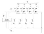
<<点灯回路15の構成>>
図3は、点灯回路15の構成の一例を示す概略ブロック図である。また、図4は、光源21~24(発光素子D1~D4)と、NMOSトランジスタQ1~Q4の接続関係を模式的に示した図である。点灯回路15は、DC-DCコンバータ40、制御回路41、断線検出回路42、ゲート駆動回路43a~43d、分圧回路44~47、NMOSトランジスタQ1~Q4、端子A~Hを備えている。<<Configuration of
Fig. 3 is a schematic block diagram showing an example of the configuration of the
DC-DCコンバータ40は、電源ラインL0に印加されるターン電圧Vtに基づいて駆動電流Ioutを生成し、出力側の電源ラインL1を介して光源20の各光源の発光素子に供給するためのコンバータである。なお、DC-DCコンバータ40には、昇降圧対応のコンバータが用いられている。The DC-
前述したように光源21~24は、電源ラインL1と、接地ラインL2との間に直列接続されて設けられている。このため、点灯させる光源の数に関わらず、DC-DCコンバータ40が供給する駆動電流Ioutは一定(例えば、200mA)である。一方、出力電圧Voutは、点灯させる光源の数に応じて変化する。本実施形態のDC-DCコンバータ40は、昇降圧対応のコンバータであり、出力電圧Voutを入力電圧(電源電圧Vbat)よりも低くする(降圧する)ことも、高くする(昇圧する)ことも可能である。本実施形態において、DC-DCコンバータ40は、「昇降圧コンバータ」に相当する。なお、昇降圧コンバータの構成については周知なので説明を省略する。As described above, the
制御回路41は、DC-DCコンバータ40の動作を制御するとともに、NMOSトランジスタQ1~Q4のオンオフを制御することにより、光源21~24のそれぞれを点灯、または消灯させる回路である。制御回路41は、シーケンシャル方式を実現させるためのタイミングを生成するタイマ回路(不図示)を備えている。例えば、DC-DCコンバータ40を動作させるタイミング(点灯のスタートのタイミング)を制御する回路(電源同期タイマ)や、信号S10~S13のレベルを順次変化させる回路(シーケンシャルタイマ)を備えている。そして、制御回路41は、ターン電圧VtがHレベルになると、信号S10~S13のレベルを、それぞれ適宜のタイミングで変化させ、NMOSトランジスタQ1~Q4のオンオフを制御する(詳細については後述)。また、制御回路41は、光源20の点灯の制御が終了したことを示す信号S1を、固定部4の点灯回路16に出力する。The
なお、制御回路41からの信号S10~S13の出力端子は、オープンドレイン出力となっており、光源21~24のそれぞれを消灯させる際には、各信号はハイ・インピーダンス状態であることとする。一方、光源21~24のそれぞれを点灯させる際には、各信号はLレベルとする。The output terminals of the signals S10 to S13 from the
断線検出回路42は、出力電圧Voutに基づいて、光源21~24の異常(ここでは発光素子D1~D4の断線)の有無を検出する回路である。例えば、電源ラインL1の出力電圧Voutを分圧する分圧抵抗(不図示)と、分圧電圧を基準電圧と比較するコンパレータ(不図示)で構成することができる。断線が生じた場合、抵抗が非常に高くなるため、分圧電圧も高くなる。よって、分圧電圧と基準電圧との比較により、断線の有無を検出することができる。断線を検出した場合、断線検出回路42は、光源20(光源21~24の何れか)に異常があることを示す(例えば、Lレベルの)信号S3をゲート駆動回路43aに出力する。The disconnection detection circuit 42 is a circuit that detects the presence or absence of an abnormality in the
ゲート駆動回路43aは、信号S2、信号S3、及び信号S10に基づいて、NMOSトランジスタQ1のゲートに印加する電圧を制御する(換言すると、NMOSトランジスタQ1のオンオフを制御する)回路であり、例えば、各信号の論理演算を行うロジック回路で構成されている。後述するように、ゲート駆動回路43aは、光源20に異常(本実施形態では発光素子D1~D4の断線)があることを示す信号S3、及び光源30に異常(発光素子D5~D8の断線)があることを示す信号S2の何れかが入力されると、信号S10に関わらず、出力をハイ・インピーダンスとし、NMOSトランジスタQ1を強制的にオンさせる。なお、ゲート駆動回路43aは、「駆動回路」に相当する。 The
また、ゲート駆動回路43bは、信号S11に基づいて、NMOSトランジスタQ2のゲートに印加する電圧を制御する。同様に、ゲート駆動回路43cは、信号S12に基づいて、NMOSトランジスタQ3のゲートに印加する電圧を制御し、ゲート駆動回路43dは、信号S13に基づいて、NMOSトランジスタQ4のゲートに印加する電圧を制御する。The
分圧回路44~47のそれぞれは、信号S10~S13のそれぞれがハイ・インピーダンス状態である場合に、NMOSトランジスタQ1~Q4をそれぞれオンさせるための回路である。分圧回路44~47は、ターン電圧Vtとして電源電圧Vbatが印加される期間、NMOSトランジスタQ1~Q4をそれぞれオンさせるべく分圧電圧を生成する。The voltage divider circuits 44 to 47 are circuits for turning on the NMOS transistors Q1 to Q4, respectively, when the signals S10 to S13 are in a high impedance state. The voltage divider circuits 44 to 47 generate divided voltages to turn on the NMOS transistors Q1 to Q4, respectively, during the period when the power supply voltage Vbat is applied as the turn voltage Vt.
具体的には、分圧回路44は、抵抗R11,R12を備えており、分圧回路45は、抵抗R13,R14を備えており、分圧回路46は、抵抗R15,R16を備えており、分圧回路47は、抵抗R17,R18を備えている。抵抗R11,R12、抵抗R13,R14、抵抗R15,R16、抵抗R17,R18のそれぞれは、ターン電圧Vtとして電源電圧Vbat(例えば12V)が印加される期間、電源電圧Vbatに基づいて生成された電圧Vcc(例えば10V)を分圧する。この際、NMOSトランジスタQ1~Q4のそれぞれをオンする分圧電圧を生成するよう、各抵抗(抵抗R11~R18)の抵抗値が設定されている。Specifically, the voltage divider circuit 44 includes resistors R11 and R12, the
NMOSトランジスタQ1~Q4は、ゲートに印加される電圧に応じてオンオフするスイッチの機能を有している。本実施形態においてNMOSトランジスタQ1~Q4は、光源21~24のそれぞれの点灯、または消灯を制御する素子である。さらに、本実施形態のNMOSトランジスタQ1は、光源21~24の全てを消灯させる機能も有している。The NMOS transistors Q1 to Q4 function as switches that turn on and off depending on the voltage applied to their gates. In this embodiment, the NMOS transistors Q1 to Q4 are elements that control the lighting or extinguishing of each of the
NMOSトランジスタQ1は、DC-DCコンバータ40と発光素子D1との間の電源ラインL1のノードN1と、接地ラインL2との間に設けられている。NMOSトランジスタQ2は、発光素子D1と発光素子D2の間の電源ラインL1のノードN2と、接地ラインL2との間に設けられている。NMOSトランジスタQ3は、発光素子D2と発光素子D3の間の電源ラインL1のノードN3と、接地ラインL2との間に設けられている。NMOSトランジスタQ4は、発光素子D3と発光素子D4の間の電源ラインL1のノードN4と、接地ラインL2との間に設けられている。 The NMOS transistor Q1 is provided between a node N1 of the power supply line L1 between the DC-
なお、NMOSトランジスタQ1は、「第1スイッチ」に相当し、NMOSトランジスタQ4は、「第2スイッチ」に相当する。また、例えば、NMOSトランジスタQ2は、「第3スイッチ」に相当する。また、ノードN4は、「第2光源の電源ライン側のノード」に相当し、ノードN2は、「第1光源の接地側のノード」に相当する。The NMOS transistor Q1 corresponds to the "first switch," and the NMOS transistor Q4 corresponds to the "second switch." For example, the NMOS transistor Q2 corresponds to the "third switch." The node N4 corresponds to the "node on the power line side of the second light source," and the node N2 corresponds to the "node on the ground side of the first light source."
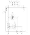
<<点灯回路16の構成>>
図5は、点灯回路16の構成の一例を示す概略ブロック図である。点灯回路16は、DC-DCコンバータ60、制御回路61、断線検出回路62、端子P~Tを備えている。<<Configuration of
5 is a schematic block diagram showing an example of the configuration of the
DC-DCコンバータ60は、電源ラインL0に印加されるターン電圧Vtに基づいて、光源30の発光素子D5~D8に駆動電流を供給するコンバータである。なお、DC-DCコンバータ60は、昇圧コンバータでもよいし、降圧コンバータでもよい。The DC-
制御回路61は、DC-DCコンバータ60の動作を制御する回路である。可動部3の点灯回路15から信号S1を受信すると、制御回路61は、DC-DCコンバータ60を動作させる。 The
断線検出回路62は、断線検出回路42と同様の回路であり、DC-DCコンバータ60の出力電圧に基づき、光源30の異常(発光素子D5~D8の断線)の有無を検出する回路である。DC-DCコンバータ60の出力電圧が所定レベルより高くなると、発光素子D5~D8の何れかが断線していると検出する。この検出結果は、光源30に異常があることを示す信号S2として点灯回路15に送信される。 The
<<点灯回路15の動作>>
図6は、点灯回路15の動作を説明するためのタイムチャートである。なお、信号S10~S13において、斜線でハッチングした部分は、ハイ・インピーダンスであることを示している。<<Operation of
6 is a time chart for explaining the operation of the
例えば、ターンシグナルランプを点滅させるための方向指示器(不図示)が操作されると、所定の周期Tx(例えば、700ms)で0V~電源電圧Vbatの間で変化するターン電圧Vtが生成され電源ラインL0に印加される。For example, when a turn signal lamp (not shown) is operated to blink the turn signal lamp, a turn voltage Vt that changes between 0 V and the power supply voltage Vbat at a predetermined period Tx (e.g., 700 ms) is generated and applied to the power supply line L0.
なお、周期Txのうち、ターン電圧Vtが0Vの期間、及び電源電圧Vbatの期間のそれぞれは、周期Txの半分の期間(350ms)であることとする。これにより、電源ラインL0には、周期Txの半分の期間、電源電圧Vbatが印加される。また、DC-DCコンバータ40は一定の駆動電流Ioutを光源21~24に供給するため、出力電圧Voutは、光源21~24が順次点灯されるにつれて階段状に高くなるよう描かれている。Note that during the cycle Tx, the period during which the turn voltage Vt is 0V and the period of the power supply voltage Vbat are each half the cycle Tx (350 ms). As a result, the power supply voltage Vbat is applied to the power supply line L0 for half the cycle Tx. In addition, since the DC-
まず、時刻t0において、ターン電圧VtがHレベル(電源電圧Vbat)になる。これにより、点灯回路15のDC-DCコンバータ40が起動し、光源20に駆動電流Ioutを供給可能な状態になる。First, at time t0, the turn voltage Vt becomes H level (power supply voltage Vbat). This starts up the DC-
点灯回路15の制御回路41は、ターン電圧VtがHレベルになると、信号S10~S13をハイ・インピーダンス状態にし、その後シーケンシャル点灯動作を開始する。なお、信号S10がハイ・インピーダンスの場合、ゲート駆動回路43aの出力もハイ・インピーダンスとなる。同様に、信号S11~S13がハイ・インピーダンスの場合、ゲート駆動回路43b~43dの出力もハイ・インピーダンスとなる。この際、分圧回路44~47のそれぞれは、NMOSトランジスタQ1~Q4のそれぞれをオンすべく分圧電圧を生成するため、電圧Vg1~Vg4のそれぞれは、NMOSトランジスタQ1~Q4のそれぞれをオンする電圧(Hレベル)となる。これにより、NMOSトランジスタQ1~Q4はオンし、光源21~24は、消灯される。When the turn voltage Vt becomes H level, the
その後、時刻t1において、制御回路41は、信号S10の出力をLレベルにする。これにより、ゲート駆動回路43aの出力がLレベルになり、分圧回路44の分圧電圧、及び電圧Vg1もLレベルになる。よって、NMOSトランジスタQ1がオフとなり、光源21が点灯する。この際、NMOSトランジスタQ2~Q4はオンしており、光源22~24は消灯されたままである。After that, at time t1, the
また、時刻t1から所定時間経過した時刻t2において、制御回路41は、信号S11の出力をLレベルにする。これにより、ゲート駆動回路43bの出力がLレベルになり、分圧回路45の分圧電圧、及び電圧Vg2がLレベルになる。よって、NMOSトランジスタQ2がオフして光源22が点灯する。なお、本実施形態において、光源22が点灯するまでは、DC-DCコンバータ40は、ターン電圧Vt(電源電圧Vbat)を降圧して、光源21,22に応じた出力電圧Voutを出力する。At time t2, a predetermined time after time t1, the
また、時刻t2から所定時間経過した時刻t3において、制御回路41は、信号S12の出力をLレベルにする。これにより、ゲート駆動回路43cの出力がLレベルになり、分圧回路46の分圧電圧、及び電圧Vg3がLレベルになる。よって、NMOSトランジスタQ3がオフして光源23が点灯する。この際には、DC-DCコンバータ40は、ターン電圧Vt(電源電圧Vbat)を昇圧して、光源21~23に応じた出力電圧Voutを出力する。At time t3, a predetermined time after time t2, the
また、時刻t3から所定時間経過した時刻t4において、制御回路41は、信号S13の出力をLレベルにする。これにより、ゲート駆動回路43dの出力がLレベルになり、分圧回路47の分圧電圧、及び電圧Vg4がLレベルになる。よって、NMOSトランジスタQ4がオフして光源24が点灯する。 At time t4, a predetermined time after time t3, the
なお、図では示していないが、制御回路41は、信号S13の出力をLレベルにした後、光源20の点灯の制御が終了したことを示す信号S1を点灯回路16に出力する。点灯回路16の制御回路61は、信号S1を受信すると、時刻t4から所定時間経過した時刻に、DC-DCコンバータ60を動作させて、光源30に駆動電流を供給させる。これにより、光源20(光源21~24)及び光源30の全てが点灯する。Although not shown in the figure, the
そして、時刻t5でターン電圧VtがLレベル(0V)になり、DC-DCコンバータ40,60の出力も0Vになる。よって、光源20(光源21~24)及び光源30の全てが消灯する。そして、時刻t6でターン電圧VtがHレベルになると、上記の時刻t0以降と同じ動作を繰り返す。 Then, at time t5, the turn voltage Vt becomes L level (0 V), and the outputs of the DC-
なお、時刻t1~t4において、光源21~24の或る発光素子が断線していることを断線検出回路42が検出した場合、断線検出回路42は、異常を示す信号S3をゲート駆動回路43aに出力する。ゲート駆動回路43aは、異常を示す信号S3を受信すると、信号S10のレベルに関わらず、ハイ・インピーダンスを出力する。よって、NMOSトランジスタQ1のゲートには分圧回路44の分圧電圧が印加され、NMOSトランジスタQ1がオンする。これにより、光源20の各光源(光源21~24)には駆動電流Ioutが流れなくなり、光源20の各光源は一斉に消灯する。If the disconnection detection circuit 42 detects that one of the
また、点灯回路16から光源30の異常を示す信号S2を受信した場合にも、ゲート駆動回路43aは、信号S10に関わらず、ハイ・インピーダンスを出力する。この場合も、NMOSトランジスタQ1がオンすることにより、光源20の各光源は一斉に消灯する。Also, when a signal S2 indicating an abnormality in the
このように、本実施形態では、NMOSトランジスタQ1をオンするだけで、光源20の全ての光源(光源21~24)を一斉に消灯させることができ、光源21~24のそれぞれを個別に消灯させる場合と比べて、消灯のタイミングのズレがなくなる。In this way, in this embodiment, all light sources (
なお、仮に、DC-DCコンバータ40が昇圧コンバータである場合、降圧できないため、光源20における駆動電流Ioutの経路の最も下流側(ここでは光源24の発光素子D4のカソード側)の電位を、DC-DCコンバータ40のプラス側の入力に印加することになる。こうすることで、点灯させる光源が少ない場合にも、DC-DCコンバータ40が、発光素子D4のカソード側の電位に基づいて、昇圧を行い、適切な出力電圧Voutを出力することができる。しかし、この場合、光源24の発光素子D4のカソード側の電位が接地電位ではないため、光源21~24の点灯、または消灯を制御するよう点灯回路を設計することが難しい。If the DC-
例えば、各光源に対して並列にNMOSトランジスタを設けると、そのNMOSトランジスタをオン状態とするための閾値電圧が高くなる。特に、直列接続された複数の光源に対してそれぞれ並列にNMOSトランジスタを設けた場合、各NMOSトランジスタの閾値電圧が異なるため制御が難しい。このため、光源に対して並列に接続するトランジスタにPMOSトランジスタを用いることになる。しかし、PMOSトランジスタでは、制御を行う回路の部品が多くなり、NMOSトランジスタの場合と比べて回路の設計が困難になる。 For example, if an NMOS transistor is provided in parallel with each light source, the threshold voltage for turning on the NMOS transistor becomes high. In particular, if an NMOS transistor is provided in parallel with each of a plurality of light sources connected in series, control is difficult because the threshold voltages of the NMOS transistors are different. For this reason, PMOS transistors are used as transistors connected in parallel with the light sources. However, with PMOS transistors, the number of components in the circuit that performs control increases, making circuit design more difficult than withNMOS transistors.
これに対し、本実施形態では、DC-DCコンバータ40が昇降圧対応であるので、光源20における電流経路の最も下流側(ここでは光源24の発光素子D4のカソード側)の電位を接地電位にすることができる。これにより、各光源(光源21~24)を点灯又は消灯させるトランジスタとしてNMOSトランジスタQ1~Q4を用いることができる。また、本実施形態においてNMOSトランジスタQ1~Q4のそれぞれは、ソースが接地されており、光源21~24に並列に接続されていない。よって、本実施形態では、NMOSトランジスタQ1~Q4を同じ電圧でオンオフ制御することができ、点灯回路15の設計が容易になる。また、前述したように、駆動電流Ioutの経路における最も上流側のNMOSトランジスタQ1をオンするだけで、光源21~24を一斉に消灯することができる。したがって、点灯回路15において、光源21~24を一斉に消灯するための回路を簡単に設計することができる。In contrast, in this embodiment, since the DC-
=====変形例=====
前述の実施形態では、光源21~24を順次点灯させていたが、これには限られない。例えば、NMOSトランジスタを全てオフにすることで光源21~24を全て点灯させた状態から、NMOSトランジスタQ4→Q3→Q2→Q1の順にオンするようにしてもよい。この場合、光源21~24が全て点灯した状態から順次消灯することになる。== ...
In the above embodiment, the
また、前述の実施形態のDC-DCコンバータ40は昇降圧コンバータであったが、これには限られない。例えば、昇圧コンバータと降圧コンバータを組み合わせて構成してもよい。この場合、昇圧コンバータでターン電圧Vtを昇圧した電圧を、降圧コンバータで降圧し、適切な出力電圧Voutを光源20に印加することができる。In addition, while the DC-
また、前述の実施形態では、車両1の可動部3と固定部4に跨るように複数の光源が配置されていたが、これには限られない。例えば、可動部3と固定部4の何れか一方に、複数の光源(及び点灯回路)を配置してシーケンシャル方式で点灯させるようにしてもよい。In addition, in the above-described embodiment, multiple light sources are arranged across the movable part 3 and
=====まとめ=====
以上、本実施形態の点灯回路15について説明した。点灯回路15は、電源ラインL1に接続された光源21と、光源21に直列接続されるとともに接地ラインL2に接続された光源24と、を含む光源20を備える点灯ユニット10に適用される点灯回路であり、電源ラインL1と、接地ラインL2とに間に設けられるNMOSトランジスタQ1と、光源24の電源ラインL1側のノードN4と、接地ラインL2との間に設けられるNMOSトランジスタQ4と、NMOSトランジスタQ1,Q4を含む複数のNMOSトランジスタのそれぞれのオンオフを制御することにより、光源21及び光源24のそれぞれを点灯、または消灯させる制御回路41を備えている。これにより、NMOSトランジスタQ1をオンすることにより、全ての光源(光源21~24)を一斉に消灯させることができる。== ...
The
また、光源21の接地側のノードN2と、接地ラインL2との間に設けられるNMOSトランジスタQ2を備え、光源20は、ノードN2と、光源24との間に設けられる光源22を含み、上記複数のNMOSトランジスタは、NMOSトランジスタQ1,Q2,Q4を含み、制御回路41は、NMOSトランジスタQ1,Q2,Q4のそれぞれのオンオフを制御することにより、光源21,22,24のそれぞれを点灯、または消灯させる。これにより、光源が3つ以上の場合でもそれぞれの点灯、消灯をそれぞれ制御できるとともに、全ての光源を一斉に消灯させることが可能である。The
また、制御回路41は、光源20に含まれる光源21~24が順次点灯するよう、NMOSトランジスタQ1をオフした後、NMOSトランジスタQ2~Q4のオンオフを制御する。これにより、光源21~24をシーケンシャル方式で順次点灯させることが可能である。In addition, the
また、制御回路41は、点灯している光源21~24が順次消灯するよう、複数のNMOSトランジスタのそれぞれのオンオフを制御した後、NMOSトランジスタQ1をオンする。これにより、光源21~24が全て点灯している状態から順次消灯させることが可能である。The
また、光源21~24に駆動電流Ioutを供給するDC-DCコンバータ40は昇降圧コンバータであり、光源21~24のそれぞれを点灯、又は消灯させるスイッチのそれぞれはNMOSトランジスタQ1~Q4で構成されている。これにより、DC-DCコンバータ40が昇降圧可能であるので、点灯させる光源の数に応じて適切な出力電圧Vout出力することができる。また、スイッチとしてNMOSトランジスタQ1~Q4を用いているので、PMOSトランジスタを用いた場合と比べて、回路構成が簡易になる。The DC-
また、光源21~24の何れかに異常があることを示す信号S3に基づいて、NMOSトランジスタQ1をオンするゲート駆動回路43aを含む。これにより、光源21~24の何れかに異常が発生した場合に、全ての光源を一斉に消灯させることができる。It also includes a
ゲート駆動回路43aは、車両1の固定部4に設けられる光源30に異常があることを示す信号S2に基づいて、NMOSトランジスタQ1をオンし、光源21~24は、固定部4に対して開閉可能な可動部3に設けられている。これにより、固定部4の光源30に異常がある場合に、可動部3の全ての光源を一斉に消灯させることができる。 The
上記の実施形態は、本発明の理解を容易にするためのものであり、本発明を限定して解釈するためのものではない。また、本発明は、その趣旨を逸脱することなく、変更や改良され得るとともに、本発明にはその等価物が含まれるのはいうまでもない。The above embodiments are intended to facilitate understanding of the present invention, and are not intended to limit the scope of the present invention. Furthermore, the present invention may be modified or improved without departing from the spirit of the present invention, and it goes without saying that the present invention includes equivalents.
1 車両
3 可動部
4 固定部
10 点灯ユニット
10A ターンシグナルランプ
11,13 可動部ユニット
12,14 固定部ユニット
15,16 点灯回路
20 光源
21~24 光源
30 光源
40,60 DC-DCコンバータ
41,61 制御回路
42,62 断線検出回路
43a~43d ゲート駆動回路
D1~D8 発光素子
Q1~Q4 NMOSトランジスタ
R11~R18 抵抗
Vt ターン電圧
L0,L1 電源ライン
L2 接地ライン1 Vehicle 3
Claims (7)
Translated fromJapanese前記電源ラインと、前記接地ラインとに間に設けられる第1スイッチと、
前記第2光源の前記電源ライン側のノードと、前記接地ラインとの間に設けられる第2スイッチと、
前記第1及び第2スイッチを含む複数のスイッチのそれぞれのオンオフを制御することにより、前記第1及び第2光源のそれぞれを点灯、または消灯させる制御回路と、
前記複数の光源に駆動電流を供給する昇降圧コンバータと、を備え、
前記複数のスイッチのそれぞれはNMOSトランジスタである、
点灯回路。 A lighting circuit applied to a vehicle lamp having a plurality of light sources including a first light source connected to a power supply line and a second light source connected in series to the first light source and connected to a ground line,
a first switch provided between the power supply line and the ground line;
a second switch provided between a node on the power supply line side of the second light source and the ground line;
a control circuit that turns on or off each of the first and second light sources by controlling on/off of each of a plurality of switches including the first and second switches;
a step-up/step-down converter for supplying a drive current to the plurality of light sources;
Each of the plurality of switches is an NMOS transistor.
Lighting circuit.
前記電源ラインと、前記接地ラインとに間に設けられる第1スイッチと、
前記第2光源の前記電源ライン側のノードと、前記接地ラインとの間に設けられる第2スイッチと、
前記第1及び第2スイッチを含む複数のスイッチのそれぞれのオンオフを制御することにより、前記第1及び第2光源のそれぞれを点灯、または消灯させる制御回路と、
前記複数の光源の何れかに異常があることを示す信号に基づいて、前記第1スイッチをオンする駆動回路と、
を備える点灯回路。A lighting circuit applied to a vehicle lamp having a plurality of light sources including a first light source connected to a power supply line and a second light source connected in series to the first light source and connected to a ground line,
a first switch provided between the power supply line and the ground line;
a second switch provided between a node on the power supply line side of the second light source and the ground line;
a control circuit that turns on or off each of the first and second light sources by controlling on/off of each of a plurality of switches including the first and second switches;
a drive circuit that turns on the first switch based on a signal indicating that any one of the plurality of light sources has an abnormality;
A lighting circuit comprising:
前記駆動回路は、
車両の固定部と、前記固定部に対して開閉可能な可動部とのうち一方に設けられる第4光源に異常があることを示す信号に基づいて、前記第1スイッチをオンし、
前記複数の光源は、前記固定部と、前記可動部とのうち他方に設けられる、
点灯回路。 3. The lighting circuit accordingto claim 2 ,
The drive circuit includes:
turning on the first switch based on a signal indicating that there is an abnormality in a fourth light source provided on one of a fixed portion of a vehicle and a movable portion that is openable and closable relative to the fixed portion;
The plurality of light sources are provided on the other of the fixed portion and the movable portion.
Lighting circuit.
前記複数の光源に駆動電流を供給する昇降圧コンバータを含み、
前記複数のスイッチのそれぞれはNMOSトランジスタである、
点灯回路。 The lighting circuit according to claim2 or3 ,
a step-up/step-down converter for supplying a drive current to the plurality of light sources;
Each of the plurality of switches is an NMOS transistor.
Lighting circuit.
前記第1光源の接地側のノードと、前記接地ラインとの間に設けられる第3スイッチとを備え、
前記複数の光源は、前記第1光源の接地側のノードと、前記第2光源との間に設けられる第3光源を含み、
前記複数のスイッチは、前記第1~第3スイッチを含み、
前記制御回路は、前記複数のスイッチのそれぞれのオンオフを制御することにより、前記第1~第3光源のそれぞれを点灯、または消灯させる、
点灯回路。 The lighting circuit according to any one of claims 1 to 4,
a third switch provided between a node on a ground side of the first light source and the ground line;
the plurality of light sources includes a third light source provided between a node on a ground side of the first light source and the second light source,
the plurality of switches include the first to third switches,
The control circuit controls the on/off of each of the plurality of switches to turn on or off each of the first to third light sources.
Lighting circuit.
前記制御回路は、前記複数の光源が順次点灯するよう、前記第1スイッチをオフした後、前記複数のスイッチのうち前記第1スイッチとは異なるスイッチのオンオフを制御する、
点灯回路。 The lighting circuit according to any one of claims 1 to 5,
the control circuit turns off the first switch, and then controls on/off of a switch other than the first switch among the plurality of switches so that the plurality of light sources are turned on in sequence;
Lighting circuit.
前記制御回路は、点灯している前記複数の光源が順次消灯するよう、前記複数のスイッチのそれぞれのオンオフを制御した後、前記第1スイッチをオンする、
点灯回路。 The lighting circuit according toany one of claims 1 to 5 ,
the control circuit controls the on/off of each of the plurality of switches so that the plurality of light sources that are turned on are sequentially turned off, and then turns on the first switch.
Lighting circuit.
Priority Applications (5)
| Application Number | Priority Date | Filing Date | Title |
|---|---|---|---|
| JP2021208016AJP7645782B2 (en) | 2021-12-22 | 2021-12-22 | Lighting circuit |
| EP22911104.2AEP4454948A4 (en) | 2021-12-22 | 2022-12-16 | LIGHTING CIRCUIT |
| CN202280083550.7ACN118541287A (en) | 2021-12-22 | 2022-12-16 | Lighting circuit |
| US18/720,356US20250042330A1 (en) | 2021-12-22 | 2022-12-16 | Lighting circuit |
| PCT/JP2022/046343WO2023120400A1 (en) | 2021-12-22 | 2022-12-16 | Lighting circuit |
Applications Claiming Priority (1)
| Application Number | Priority Date | Filing Date | Title |
|---|---|---|---|
| JP2021208016AJP7645782B2 (en) | 2021-12-22 | 2021-12-22 | Lighting circuit |
Publications (3)
| Publication Number | Publication Date |
|---|---|
| JP2023092798A JP2023092798A (en) | 2023-07-04 |
| JP2023092798A5 JP2023092798A5 (en) | 2024-11-14 |
| JP7645782B2true JP7645782B2 (en) | 2025-03-14 |
Family
ID=86902602
Family Applications (1)
| Application Number | Title | Priority Date | Filing Date |
|---|---|---|---|
| JP2021208016AActiveJP7645782B2 (en) | 2021-12-22 | 2021-12-22 | Lighting circuit |
Country Status (5)
| Country | Link |
|---|---|
| US (1) | US20250042330A1 (en) |
| EP (1) | EP4454948A4 (en) |
| JP (1) | JP7645782B2 (en) |
| CN (1) | CN118541287A (en) |
| WO (1) | WO2023120400A1 (en) |
Families Citing this family (1)
| Publication number | Priority date | Publication date | Assignee | Title |
|---|---|---|---|---|
| JP2025062170A (en)* | 2023-10-02 | 2025-04-14 | 株式会社小糸製作所 | Lighting circuit, lighting device, and method for manufacturing the lighting circuit |
Citations (3)
| Publication number | Priority date | Publication date | Assignee | Title |
|---|---|---|---|---|
| JP2013243147A (en) | 2009-02-17 | 2013-12-05 | Luminature Co Ltd | Power-saving led lighting apparatus |
| JP2015145224A (en) | 2014-02-04 | 2015-08-13 | 株式会社小糸製作所 | Vehicular lighting fixture |
| KR101598131B1 (en) | 2013-05-01 | 2016-03-08 | 그린칩 주식회사 | Apparatus for Cross Drive Control of LED lighting |
Family Cites Families (8)
| Publication number | Priority date | Publication date | Assignee | Title |
|---|---|---|---|---|
| JP4931720B2 (en)* | 2007-07-26 | 2012-05-16 | 株式会社小糸製作所 | Lighting control device for vehicle lamp |
| JP2010109168A (en)* | 2008-10-30 | 2010-05-13 | Fuji Electric Systems Co Ltd | Led driving device, led driving method, and lighting device |
| US8569956B2 (en)* | 2009-06-04 | 2013-10-29 | Point Somee Limited Liability Company | Apparatus, method and system for providing AC line power to lighting devices |
| US8686651B2 (en)* | 2011-04-13 | 2014-04-01 | Supertex, Inc. | Multiple stage sequential current regulator |
| TWI477190B (en)* | 2012-08-10 | 2015-03-11 | Macroblock Inc | Light emitting diode driving apparatus |
| CN109688666B (en) | 2014-12-24 | 2021-04-20 | 株式会社小糸制作所 | Light source lighting circuit and turn signal lamp |
| KR102300560B1 (en)* | 2015-06-26 | 2021-09-14 | 삼성전자주식회사 | Led driving apparatus and lighting apparatus including the same |
| JP6800581B2 (en) | 2015-12-28 | 2020-12-16 | 株式会社小糸製作所 | Lighting circuit, turn signal lamp for vehicles |
- 2021
- 2021-12-22JPJP2021208016Apatent/JP7645782B2/enactiveActive
- 2022
- 2022-12-16EPEP22911104.2Apatent/EP4454948A4/enactivePending
- 2022-12-16USUS18/720,356patent/US20250042330A1/enactivePending
- 2022-12-16WOPCT/JP2022/046343patent/WO2023120400A1/ennot_activeCeased
- 2022-12-16CNCN202280083550.7Apatent/CN118541287A/enactivePending
Patent Citations (3)
| Publication number | Priority date | Publication date | Assignee | Title |
|---|---|---|---|---|
| JP2013243147A (en) | 2009-02-17 | 2013-12-05 | Luminature Co Ltd | Power-saving led lighting apparatus |
| KR101598131B1 (en) | 2013-05-01 | 2016-03-08 | 그린칩 주식회사 | Apparatus for Cross Drive Control of LED lighting |
| JP2015145224A (en) | 2014-02-04 | 2015-08-13 | 株式会社小糸製作所 | Vehicular lighting fixture |
Also Published As
| Publication number | Publication date |
|---|---|
| US20250042330A1 (en) | 2025-02-06 |
| JP2023092798A (en) | 2023-07-04 |
| EP4454948A4 (en) | 2025-04-30 |
| EP4454948A1 (en) | 2024-10-30 |
| WO2023120400A1 (en) | 2023-06-29 |
| CN118541287A (en) | 2024-08-23 |
Similar Documents
| Publication | Publication Date | Title |
|---|---|---|
| KR101932873B1 (en) | Switch driving device, light emitting device, vehicle | |
| US9420671B1 (en) | Lighting control system | |
| US7323831B2 (en) | Illumination device | |
| TWI631791B (en) | Switching charging circuit | |
| JP4975038B2 (en) | CIRCUIT DEVICE AND CIRCUIT DEVICE DRIVE METHOD | |
| EP2457768B1 (en) | Power converter and vehicle lighting device, vehicle headlight and vehicle using power converter | |
| JP7645782B2 (en) | Lighting circuit | |
| JP2004168076A (en) | Vehicular turn signal indicator system and flasher circuit for the same | |
| CN107205295A (en) | Light-emitting component drive apparatus, light-emitting device, vehicle | |
| KR20180125437A (en) | Multiple LED string dimming control | |
| CN107666740A (en) | Lighting circuit and lamps apparatus for vehicle | |
| JP6186270B2 (en) | Vehicle lighting | |
| JP7542375B2 (en) | Vehicle lighting system | |
| JP7565298B2 (en) | Light-emitting control system, light-emitting system, light-emitting control device, and light-emitting device | |
| JP2020059430A (en) | Vehicle light control device | |
| CN103250468B (en) | LED flash-generating device and LED flash-generating method | |
| JP2023092798A5 (en) | ||
| CN114263888B (en) | Light control module, vehicle lighting, signal processing device | |
| WO2022133671A1 (en) | Light assembly for performing lighting functions with switching units in low side position | |
| JP7620184B2 (en) | Lighting equipment | |
| JP7274943B2 (en) | Sequential light emitting device and control device | |
| CN113243143B (en) | Method for limiting current surges in automotive lighting devices | |
| WO2022133672A1 (en) | Light assembly for powering lighting functions with different power requirements | |
| EP4529359A1 (en) | Lighting device and vehicle lamp | |
| JPS585633Y2 (en) | Vehicle light control device |
Legal Events
| Date | Code | Title | Description |
|---|---|---|---|
| A621 | Written request for application examination | Free format text:JAPANESE INTERMEDIATE CODE: A621 Effective date:20241022 | |
| A521 | Request for written amendment filed | Free format text:JAPANESE INTERMEDIATE CODE: A523 Effective date:20241106 | |
| A131 | Notification of reasons for refusal | Free format text:JAPANESE INTERMEDIATE CODE: A131 Effective date:20241119 | |
| A521 | Request for written amendment filed | Free format text:JAPANESE INTERMEDIATE CODE: A523 Effective date:20250117 | |
| TRDD | Decision of grant or rejection written | ||
| A01 | Written decision to grant a patent or to grant a registration (utility model) | Free format text:JAPANESE INTERMEDIATE CODE: A01 Effective date:20250225 | |
| A61 | First payment of annual fees (during grant procedure) | Free format text:JAPANESE INTERMEDIATE CODE: A61 Effective date:20250304 | |
| R150 | Certificate of patent or registration of utility model | Ref document number:7645782 Country of ref document:JP Free format text:JAPANESE INTERMEDIATE CODE: R150 |