JP7645296B2 - Iodine-containing metal compound and composition for thin film deposition containing the same - Google Patents
Iodine-containing metal compound and composition for thin film deposition containing the sameDownload PDFInfo
- Publication number
- JP7645296B2 JP7645296B2JP2023016388AJP2023016388AJP7645296B2JP 7645296 B2JP7645296 B2JP 7645296B2JP 2023016388 AJP2023016388 AJP 2023016388AJP 2023016388 AJP2023016388 AJP 2023016388AJP 7645296 B2JP7645296 B2JP 7645296B2
- Authority
- JP
- Japan
- Prior art keywords
- alkyl
- thin film
- metal
- independently
- composition
- Prior art date
- Legal status (The legal status is an assumption and is not a legal conclusion. Google has not performed a legal analysis and makes no representation as to the accuracy of the status listed.)
- Active
Links
Images


Classifications
- G—PHYSICS
- G03—PHOTOGRAPHY; CINEMATOGRAPHY; ANALOGOUS TECHNIQUES USING WAVES OTHER THAN OPTICAL WAVES; ELECTROGRAPHY; HOLOGRAPHY
- G03F—PHOTOMECHANICAL PRODUCTION OF TEXTURED OR PATTERNED SURFACES, e.g. FOR PRINTING, FOR PROCESSING OF SEMICONDUCTOR DEVICES; MATERIALS THEREFOR; ORIGINALS THEREFOR; APPARATUS SPECIALLY ADAPTED THEREFOR
- G03F7/00—Photomechanical, e.g. photolithographic, production of textured or patterned surfaces, e.g. printing surfaces; Materials therefor, e.g. comprising photoresists; Apparatus specially adapted therefor
- G03F7/004—Photosensitive materials
- C—CHEMISTRY; METALLURGY
- C01—INORGANIC CHEMISTRY
- C01G—COMPOUNDS CONTAINING METALS NOT COVERED BY SUBCLASSES C01D OR C01F
- C01G19/00—Compounds of tin
- C01G19/02—Oxides
- C—CHEMISTRY; METALLURGY
- C01—INORGANIC CHEMISTRY
- C01G—COMPOUNDS CONTAINING METALS NOT COVERED BY SUBCLASSES C01D OR C01F
- C01G30/00—Compounds of antimony
- C01G30/004—Oxides; Hydroxides; Oxyacids
- C01G30/005—Oxides
- C—CHEMISTRY; METALLURGY
- C07—ORGANIC CHEMISTRY
- C07F—ACYCLIC, CARBOCYCLIC OR HETEROCYCLIC COMPOUNDS CONTAINING ELEMENTS OTHER THAN CARBON, HYDROGEN, HALOGEN, OXYGEN, NITROGEN, SULFUR, SELENIUM OR TELLURIUM
- C07F5/00—Compounds containing elements of Groups 3 or 13 of the Periodic Table
- C—CHEMISTRY; METALLURGY
- C07—ORGANIC CHEMISTRY
- C07F—ACYCLIC, CARBOCYCLIC OR HETEROCYCLIC COMPOUNDS CONTAINING ELEMENTS OTHER THAN CARBON, HYDROGEN, HALOGEN, OXYGEN, NITROGEN, SULFUR, SELENIUM OR TELLURIUM
- C07F5/00—Compounds containing elements of Groups 3 or 13 of the Periodic Table
- C07F5/003—Compounds containing elements of Groups 3 or 13 of the Periodic Table without C-Metal linkages
- C—CHEMISTRY; METALLURGY
- C07—ORGANIC CHEMISTRY
- C07F—ACYCLIC, CARBOCYCLIC OR HETEROCYCLIC COMPOUNDS CONTAINING ELEMENTS OTHER THAN CARBON, HYDROGEN, HALOGEN, OXYGEN, NITROGEN, SULFUR, SELENIUM OR TELLURIUM
- C07F7/00—Compounds containing elements of Groups 4 or 14 of the Periodic Table
- C07F7/22—Tin compounds
- C07F7/2284—Compounds with one or more Sn-N linkages
- C—CHEMISTRY; METALLURGY
- C07—ORGANIC CHEMISTRY
- C07F—ACYCLIC, CARBOCYCLIC OR HETEROCYCLIC COMPOUNDS CONTAINING ELEMENTS OTHER THAN CARBON, HYDROGEN, HALOGEN, OXYGEN, NITROGEN, SULFUR, SELENIUM OR TELLURIUM
- C07F9/00—Compounds containing elements of Groups 5 or 15 of the Periodic Table
- C07F9/90—Antimony compounds
- C07F9/902—Compounds without antimony-carbon linkages
- C—CHEMISTRY; METALLURGY
- C23—COATING METALLIC MATERIAL; COATING MATERIAL WITH METALLIC MATERIAL; CHEMICAL SURFACE TREATMENT; DIFFUSION TREATMENT OF METALLIC MATERIAL; COATING BY VACUUM EVAPORATION, BY SPUTTERING, BY ION IMPLANTATION OR BY CHEMICAL VAPOUR DEPOSITION, IN GENERAL; INHIBITING CORROSION OF METALLIC MATERIAL OR INCRUSTATION IN GENERAL
- C23C—COATING METALLIC MATERIAL; COATING MATERIAL WITH METALLIC MATERIAL; SURFACE TREATMENT OF METALLIC MATERIAL BY DIFFUSION INTO THE SURFACE, BY CHEMICAL CONVERSION OR SUBSTITUTION; COATING BY VACUUM EVAPORATION, BY SPUTTERING, BY ION IMPLANTATION OR BY CHEMICAL VAPOUR DEPOSITION, IN GENERAL
- C23C16/00—Chemical coating by decomposition of gaseous compounds, without leaving reaction products of surface material in the coating, i.e. chemical vapour deposition [CVD] processes
- C23C16/22—Chemical coating by decomposition of gaseous compounds, without leaving reaction products of surface material in the coating, i.e. chemical vapour deposition [CVD] processes characterised by the deposition of inorganic material, other than metallic material
- C23C16/30—Deposition of compounds, mixtures or solid solutions, e.g. borides, carbides, nitrides
- C23C16/40—Oxides
- C23C16/407—Oxides of zinc, germanium, cadmium, indium, tin, thallium or bismuth
- C—CHEMISTRY; METALLURGY
- C23—COATING METALLIC MATERIAL; COATING MATERIAL WITH METALLIC MATERIAL; CHEMICAL SURFACE TREATMENT; DIFFUSION TREATMENT OF METALLIC MATERIAL; COATING BY VACUUM EVAPORATION, BY SPUTTERING, BY ION IMPLANTATION OR BY CHEMICAL VAPOUR DEPOSITION, IN GENERAL; INHIBITING CORROSION OF METALLIC MATERIAL OR INCRUSTATION IN GENERAL
- C23C—COATING METALLIC MATERIAL; COATING MATERIAL WITH METALLIC MATERIAL; SURFACE TREATMENT OF METALLIC MATERIAL BY DIFFUSION INTO THE SURFACE, BY CHEMICAL CONVERSION OR SUBSTITUTION; COATING BY VACUUM EVAPORATION, BY SPUTTERING, BY ION IMPLANTATION OR BY CHEMICAL VAPOUR DEPOSITION, IN GENERAL
- C23C16/00—Chemical coating by decomposition of gaseous compounds, without leaving reaction products of surface material in the coating, i.e. chemical vapour deposition [CVD] processes
- C23C16/44—Chemical coating by decomposition of gaseous compounds, without leaving reaction products of surface material in the coating, i.e. chemical vapour deposition [CVD] processes characterised by the method of coating
- C23C16/455—Chemical coating by decomposition of gaseous compounds, without leaving reaction products of surface material in the coating, i.e. chemical vapour deposition [CVD] processes characterised by the method of coating characterised by the method used for introducing gases into reaction chamber or for modifying gas flows in reaction chamber
- C23C16/45523—Pulsed gas flow or change of composition over time
- C23C16/45525—Atomic layer deposition [ALD]
- C23C16/45527—Atomic layer deposition [ALD] characterized by the ALD cycle, e.g. different flows or temperatures during half-reactions, unusual pulsing sequence, use of precursor mixtures or auxiliary reactants or activations
- C23C16/45536—Use of plasma, radiation or electromagnetic fields
- C—CHEMISTRY; METALLURGY
- C23—COATING METALLIC MATERIAL; COATING MATERIAL WITH METALLIC MATERIAL; CHEMICAL SURFACE TREATMENT; DIFFUSION TREATMENT OF METALLIC MATERIAL; COATING BY VACUUM EVAPORATION, BY SPUTTERING, BY ION IMPLANTATION OR BY CHEMICAL VAPOUR DEPOSITION, IN GENERAL; INHIBITING CORROSION OF METALLIC MATERIAL OR INCRUSTATION IN GENERAL
- C23C—COATING METALLIC MATERIAL; COATING MATERIAL WITH METALLIC MATERIAL; SURFACE TREATMENT OF METALLIC MATERIAL BY DIFFUSION INTO THE SURFACE, BY CHEMICAL CONVERSION OR SUBSTITUTION; COATING BY VACUUM EVAPORATION, BY SPUTTERING, BY ION IMPLANTATION OR BY CHEMICAL VAPOUR DEPOSITION, IN GENERAL
- C23C16/00—Chemical coating by decomposition of gaseous compounds, without leaving reaction products of surface material in the coating, i.e. chemical vapour deposition [CVD] processes
- C23C16/44—Chemical coating by decomposition of gaseous compounds, without leaving reaction products of surface material in the coating, i.e. chemical vapour deposition [CVD] processes characterised by the method of coating
- C23C16/455—Chemical coating by decomposition of gaseous compounds, without leaving reaction products of surface material in the coating, i.e. chemical vapour deposition [CVD] processes characterised by the method of coating characterised by the method used for introducing gases into reaction chamber or for modifying gas flows in reaction chamber
- C23C16/45523—Pulsed gas flow or change of composition over time
- C23C16/45525—Atomic layer deposition [ALD]
- C23C16/45553—Atomic layer deposition [ALD] characterized by the use of precursors specially adapted for ALD
Landscapes
- Chemical & Material Sciences (AREA)
- Organic Chemistry (AREA)
- Engineering & Computer Science (AREA)
- Inorganic Chemistry (AREA)
- General Chemical & Material Sciences (AREA)
- Chemical Kinetics & Catalysis (AREA)
- Materials Engineering (AREA)
- Mechanical Engineering (AREA)
- Metallurgy (AREA)
- Physics & Mathematics (AREA)
- Electromagnetism (AREA)
- Plasma & Fusion (AREA)
- General Physics & Mathematics (AREA)
- Chemical Vapour Deposition (AREA)
- Formation Of Insulating Films (AREA)
- Chemically Coating (AREA)
Description
Translated fromJapanese本開示は、ヨウ素を含む金属化合物、これを含む金属含有薄膜蒸着用組成物、および前記薄膜蒸着用組成物を用いた金属含有薄膜の製造方法に関する。The present disclosure relates to a metal compound containing iodine, a composition for metal-containing thin film deposition containing the same, and a method for producing a metal-containing thin film using the composition for thin film deposition.
現在使用されているフォトレジストであるCAR(Chemically amplified resist)は、高い敏感度(sensitivity)のために設計されているが、一般的な元素構成(主に、より少ない量(smaller quantities)のO、F、Sを有する、C)が13.5nmの波長でフォトレジストを過剰に透明にすることによって敏感度を減少させる現象が現れ得る。Currently used photoresists, CAR (chemically amplified resist), are designed for high sensitivity, but common elemental compositions (mainly C with smaller quantities of O, F, S) can reduce sensitivity by making the photoresist too transparent at 13.5 nm wavelengths.
また、CARは、小さいピッチャーサイズで粗さ(roughness)の問題によって工程上効率が減少するか、酸触媒を用いた工程で光速度(photospeed)が減少するにつれてLER(Line edge roughness)が増加することが報告されており、これを解決するために、EUV(extreme ultroviolet)リソグラフィのための無機化合物(inorganic compounds)が求められている(韓国公開特許KR10-2022-0000366A)。In addition, it has been reported that CAR has a problem of roughness due to small pitcher size, which reduces process efficiency, and that LER (line edge roughness) increases as the photospeed decreases in processes using acid catalysts. To solve this problem, inorganic compounds for EUV (extreme ultraviolet) lithography are required (Korean Patent Publication KR10-2022-0000366A).
一実施形態は、金属含有薄膜の前駆物質として使用可能なヨウ素含有金属化合物およびこれを含む金属含有薄膜蒸着用組成物を提供する。One embodiment provides an iodine-containing metal compound that can be used as a precursor for a metal-containing thin film, and a composition for vapor deposition of a metal-containing thin film that includes the same.
他の一実施形態は、前記金属含有薄膜蒸着用組成物を用いた金属含有薄膜の製造方法を提供する。Another embodiment provides a method for producing a metal-containing thin film using the metal-containing thin film deposition composition.
一実施形態は、下記化学式1で表される化合物を提供する。
[化学式1]
Mは、第14族金属、第15族金属または第16族金属であり、
R1は、水素またはC1-7アルキルであり、
R2は、C1-7アルキルであり、
R3およびR4は、それぞれ独立して、C1-7アルキル、C2-7アルケニルまたは-NR5R6であり、前記R5およびR6は、それぞれ独立して、水素またはC1-7アルキルであり、
Mの金属酸化数に応じて、前記R3およびR4は、それぞれ独立して存在しなくてもよい。 One embodiment provides a compound represented by the following formula 1:
[Chemical Formula 1]
M is a Group 14, 15 or 16 metal;
R1 is hydrogen or C1-7 alkyl;
R2 isC1-7 alkyl;
R3 and R4 are each independently C1-7 alkyl, C2-7 alkenyl, or -NR5 R6 , wherein R5 and R6 are each independently hydrogen or C1-7 alkyl;
Depending on the metal oxidation number of M,R3 andR4 may each independently be absent.
他の一実施形態は、前記一実施形態によるヨウ素含有金属化合物を含む金属含有薄膜蒸着用組成物を提供する。Another embodiment provides a composition for metal-containing thin film deposition comprising the iodine-containing metal compound according to the above embodiment.
他の一実施形態は、前記一実施形態による金属含有薄膜蒸着用組成物を用いる金属含有薄膜の製造方法を提供する。Another embodiment provides a method for producing a metal-containing thin film using the composition for depositing a metal-containing thin film according to the embodiment.
本開示は、ヨウ素を含有する金属化合物、これを含む金属含有薄膜蒸着用組成物およびこれを用いた金属含有薄膜の製造方法に関し、一実施形態による薄膜蒸着用組成物は、常温で液体状態で存在して保管および取り扱いに優れ、高い反応性を有することから、これを用いて金属薄膜を効率的に形成することができる。The present disclosure relates to a metal compound containing iodine, a composition for metal-containing thin film deposition containing the same, and a method for producing a metal-containing thin film using the same. The composition for thin film deposition according to one embodiment exists in a liquid state at room temperature, has excellent storage and handling properties, and has high reactivity, so that a metal thin film can be efficiently formed using the composition.
本明細書に記載の実施形態は、様々な他の形態に変形可能であり、一実施形態による技術が以下に説明する実施形態に限定されない。さらに、明細書の全体においてある構成要素を「含む」、「備える」、「含有する」、または「有する」とは、特別に反対の記載がない限り、他の構成要素を除くのではなく、他の構成要素をさらに含み得ることを意味し、さらに挙げられていない要素、材料または工程を排除しない。The embodiments described herein may be modified in various other forms, and the technology according to one embodiment is not limited to the embodiments described below. Furthermore, throughout the specification, "including," "comprising," "containing," or "having" a certain element means that it may further include other elements, but does not exclude other elements, materials, or steps not further recited, unless specifically stated to the contrary.
本明細書で使用される数値範囲は、下限値と上限値とその範囲内でのすべての値、定義される範囲の形態と幅で論理的に誘導される増分、二重限定されたすべての値および互いに異なる形態に限定された数値範囲の上限および下限のすべての可能な組み合わせを含む。一例として、組成の含量が10%~80%または20%~50%に限定された場合、10%~50%または50%~80%の数値範囲も本明細書に記載のものとして解釈すべきである。本明細書で特別な定義がない限り、実験誤差または値の四捨五入によって発生する可能性がある数値範囲以外の値も定義された数値範囲に含まれる。Numerical ranges used herein include lower and upper limits and all values within the range, increments logically derived by the form and width of the range defined, all doubly limited values, and all possible combinations of upper and lower limits of numerical ranges limited in different forms. As an example, if the content of a composition is limited to 10% to 80% or 20% to 50%, the numerical ranges of 10% to 50% or 50% to 80% should also be interpreted as being described herein. Unless otherwise specified in this specification, values outside the numerical ranges that may occur due to experimental error or rounding of values are included in the defined numerical range.
以下、本明細書において特別な定義がない限り、「約」は、明示されている値の30%、25%、20%、15%、10%または5%以内の値として考えられる。Hereinafter, unless otherwise defined in this specification, "about" is considered to mean a value within 30%, 25%, 20%, 15%, 10% or 5% of the specified value.
本明細書において、「アルキル」は、炭素および水素原子のみで構成された直鎖または分岐鎖の炭化水素を意味し、1個~7個、1個~5個または1個~4個の炭素を有することができる。As used herein, "alkyl" means a straight or branched chain hydrocarbon composed solely of carbon and hydrogen atoms and can have 1 to 7, 1 to 5, or 1 to 4 carbons.
本の明細書において、「アルケニル」は、鎖の任意の位置に一つまたは多数の炭素-炭素二重結合を有する炭化水素を意味し、単一置換または多重置換されることができる。例えば、アルケニル基は、ビニル基、プロペニル基、ブテニル基、ペンテニル基、ヘキセニル基、ブタジエニル基、ペンタジエニル基、ヘキサジエニル基などを含むことができる。As used herein, "alkenyl" means a hydrocarbon having one or more carbon-carbon double bonds at any position in the chain, which may be singly or multiply substituted. For example, alkenyl groups may include vinyl, propenyl, butenyl, pentenyl, hexenyl, butadienyl, pentadienyl, hexadienyl, and the like.
本明細書において、「脱離基(leavinggroup)」は、他の官能基または原子による置換反応(例えば、親核性置換反応)により置換されることができる官能基または原子を指し、例えば、モノC1-7アルキルアミンまたはジC1-7アルキルアミンであってもよく、これに限定されるものではない。 As used herein, a "leaving group" refers to a functional group or atom that can be replaced by a substitution reaction (e.g., a nucleophilic substitution reaction) with another functional group or atom, and may be, for example, but is not limited to, a mono-C1-7 alkylamine or a di-C1-7 alkylamine.
本明細書において、「ジアルキルアミン」に含まれる二つのアルキル基は、同一であってもよく、相違していてもよい。In this specification, the two alkyl groups contained in a "dialkylamine" may be the same or different.
一実施形態は、下記化学式1で表されるヨウ素含有金属化合物を提供する。One embodiment provides an iodine-containing metal compound represented by the following chemical formula 1:
[化学式1]
前記化学式1中、
Mは、第14族金属、第15族金属または第16族金属であり、
R1は、水素またはC1-7アルキルであり、
R2は、C1-7アルキルであり、
R3およびR4は、それぞれ独立して、C1-7アルキル、C2-7アルケニルまたは-NR5R6であり、前記R5およびR6は、それぞれ独立して、水素またはC1-7アルキルであり、
Mの金属酸化数に応じて、前記R3およびR4は、それぞれ独立して存在しなくてもよい。 In the above Chemical Formula 1,
M is a Group 14, 15 or 16 metal;
R1 is hydrogen or C1-7 alkyl;
R2 isC1-7 alkyl;
R3 and R4 are each independently C1-7 alkyl, C2-7 alkenyl, or -NR5 R6 , wherein R5 and R6 are each independently hydrogen or C1-7 alkyl;
Depending on the metal oxidation number of M,R3 andR4 may each independently be absent.
一実施形態によるヨウ素含有金属化合物は、金属にモノアルキルアミノまたはジアルキルアミノ基とヨウ素基がともに導入されることにより、薄膜蒸着用前駆体として使用される場合、向上した物性を有する金属含有薄膜を製造することができる。一実施形態において、前記ヨウ素含有金属化合物は、ヨウ素および金属を含有することにより、EUVに対する光吸収率および/または光放出率の効果に優れ、フォトリソグラフィ工程に使用されるハードマスクとして有効に使用されることができる。In one embodiment, the iodine-containing metal compound has both a monoalkylamino or dialkylamino group and an iodine group introduced into the metal, and when used as a precursor for thin film deposition, it can produce a metal-containing thin film with improved physical properties. In one embodiment, the iodine-containing metal compound contains iodine and a metal, and therefore has excellent effects in terms of light absorptivity and/or light emissivity for EUV, and can be effectively used as a hard mask for use in photolithography processes.
一実施形態において、前記R1およびR2は、それぞれ独立して、直鎖または分岐鎖のC1-7アルキル、C1-5アルキル、C1-4アルキル、C1-3アルキル、C1-2アルキルまたはメチルであることができる。 In one embodiment, said R1 and R2 may each independently be a straight or branched chain C1-7 alkyl, C1-5 alkyl, C1-4 alkyl, C1-3 alkyl, C1-2 alkyl or methyl.
一実施形態において、前記R3およびR4は、それぞれ独立して、直鎖または分岐鎖のC1-7アルキル、C1-6アルキル、C1-5アルキル、C1-4アルキル、C1-3アルキル、C1-2アルキル、メチル、C2-7アルケニル、C2-6アルケニル、C2-5アルケニル、C2-4アルケニル、C2-3アルケニルまたはビニル(エテニル)であることができる。ここで、前記アルケニルは、不飽和炭素が直接連結されるか、または不飽和炭素がアルキレンを挟んで連結されたものを含む。また、一実施形態において、前記R3およびR4は、それぞれ独立して、-NR5R6であることができ、ここで、R5およびR6は、それぞれ独立して、水素または直鎖または分岐鎖のC1-7アルキル、C1-6アルキル、C1-5アルキル、C1-4アルキル、C1-3アルキル、C1-2アルキルまたはメチルであることができる。 In one embodiment,R3 andR4 may each independently be a linear or branchedC1-7 alkyl, C1-6alkyl ,C1-5 alkyl,C1-4 alkyl,C1-3 alkyl,C1-2 alkyl, methyl,C2-7 alkenyl,C2-6 alkenyl,C2-5 alkenyl,C2-4 alkenyl,C2-3 alkenyl, or vinyl (ethenyl), where the alkenyl includes those in which the unsaturated carbon is directly linked or the unsaturated carbon is linked via an alkylene. Also, in one embodiment, R3 and R4 can each independently be -NR5 R6 , where R5 and R6 can each independently be hydrogen or a straight or branched chain C1-7 alkyl, C1-6 alkyl, C1-5 alkyl, C1-4 alkyl, C1-3 alkyl, C1-2 alkyl or methyl.
一実施形態において、前記Mは、Si、Ge、Sn、Pb、P、As、Sb、Bi、S、Se、TeまたはPoであることができ、前記Mの金属酸化数に応じて、前記R3および/またはR4は、それぞれ独立して存在しなくてもよい。 In one embodiment, M can be Si, Ge, Sn, Pb, P, As, Sb, Bi, S, Se, Te or Po, and depending on the metal oxidation number of M,R3 and/orR4 may each independently be absent.
一実施形態において、前記ヨウ素金属化合物は、下記化学式2で表される化合物であることができる。In one embodiment, the iodine metal compound may be a compound represented by the following chemical formula 2:
[化学式2]
前記化学式2中、
M1は、第14族金属であり、
R11は、水素またはC1-7アルキルであり、
R12は、C1-7アルキルであり、
R13およびR14は、それぞれ独立して、C1-7アルキル、C2-7アルケニルまたは-NR15R16であり、前記R15およびR16は、それぞれ独立して、水素またはC1-7アルキルであってもよい。
一実施形態において、前記M1は、SnまたはSbであることができる。
一実施形態において、前記R11およびR13は、それぞれ独立して、直鎖または分岐鎖のC1-7アルキル、C1-5アルキル、C1-4アルキル、C1-3アルキル、C1-2アルキルまたはメチルであることができる。
In the above Chemical Formula 2,
M1 is a Group 14 metal;
R11 is hydrogen or C1-7 alkyl;
R12 is C1-7 alkyl;
R13 and R14 are each independently C1-7 alkyl, C2-7 alkenyl or -NR15 R16 , wherein R15 and R16 may each independently be hydrogen or C1-7 alkyl.
In one embodiment,M1 can be Sn orSb .
In one embodiment, said R11 and R13 can each independently be a straight or branched chain C1-7 alkyl, C1-5 alkyl, C1-4 alkyl, C1-3 alkyl, C1-2 alkyl or methyl.
一実施形態において、前記R13およびR14は、それぞれ独立して、直鎖または分岐鎖のC1-7アルキル、C1-6アルキル、C1-5アルキル、C1-4アルキル、C1-3アルキル、C1-2アルキル、メチル、C2-7アルケニル、C2-6アルケニル、C2-5アルケニル、C2-4アルケニル、C2-3アルケニルまたはビニル(エテニル)であることができる。ここで、前記アルケニルは、不飽和炭素が直接連結されるか、または不飽和炭素がアルキレンを挟んで連結されたものを含む。また、一実施形態において、前記R13およびR14は、それぞれ独立して、-NR15R16であることができ、ここで、R15およびR16は、それぞれ独立して、水素または直鎖または分岐鎖のC1-7アルキル、C1-6アルキル、C1-5アルキル、C1-4アルキル、C1-3アルキル、C1-2アルキルまたはメチルであることができる。 In one embodiment, R13 and R14 may each independently be a linear or branched C1-7 alkyl, C1-6 alkyl, C1-5 alkyl, C1-4 alkyl, C1-3 alkyl, C 1-2 alkyl, methyl, C2-7 alkenyl, C2-6 alkenyl, C2-5 alkenyl, C2-4 alkenyl,C 2-3alkenyl , or vinyl (ethenyl), where the alkenyl includes those in which the unsaturated carbon is directly linked or the unsaturated carbon is linked via an alkylene. In one embodiment, R13 and R14 can each independently be -NR15 R16 , where R15 and R16 can each independently be hydrogen or a straight or branched chain C1-7 alkyl, C1-6 alkyl, C1-5 alkyl, C1-4 alkyl, C1-3 alkyl, C1-2 alkyl or methyl.
一実施形態において、前記ヨウ素金属化合物は、下記化学式3で表される化合物であることができる。In one embodiment, the iodine metal compound may be a compound represented by the following chemical formula 3:
[化学式3]
前記化学式3中、
M2は、第15族金属であり、
R21は、水素またはC1-7アルキルであり、
R22は、C1-7アルキルであり、
R23は、C1-7アルキル、C2-7アルケニルまたは-NR25R26であり、前記R25およびR26は、それぞれ独立して、水素またはC1-7アルキルであってもよい。 In the above Chemical Formula 3,
M2 is a Group 15 metal;
R21 is hydrogen or C1-7 alkyl;
R22 is C1-7 alkyl;
R23 is C1-7 alkyl, C2-7 alkenyl or —NR25 R26 , wherein R25 and R26 may each independently be hydrogen or C1-7 alkyl.
一実施形態において、前記M2は、SbまたはBiであることができる。 In one embodiment,M2 can be Sb or Bi.
一実施形態において、前記R21およびR22は、それぞれ独立して、直鎖または分岐鎖のC1-7アルキル、C1-5アルキル、C1-4アルキル、C1-3アルキル、C1-2アルキルまたはメチルであることができる。 In one embodiment, R21 and R22 may each independently be a straight or branched chain C1-7 alkyl, C1-5 alkyl, C1-4 alkyl, C1-3 alkyl, C1-2 alkyl or methyl.
一実施形態において、前記R23は、直鎖または分岐鎖のC1-7アルキル、C1-6アルキル、C1-5アルキル、C1-4アルキル、C1-3アルキル、C1-2アルキル、メチル、C2-7アルケニル、C2-6アルケニル、C2-5アルケニル、C2-4アルケニル、C2-3アルケニルまたはビニル(エテニル)であることができる。ここで、前記アルケニルは、不飽和炭素が直接連結されるか、または不飽和炭素がアルキレンを挟んで連結されたものを含む。また、一実施形態において、前記R23は、-NR25R26であることができ、ここで、R25およびR26は、それぞれ独立して、水素または直鎖または分岐鎖のC1-7アルキル、C1-6アルキル、C1-5アルキル、C1-4アルキル、C1-3アルキル、C1-2アルキルまたはメチルであることができる。 In one embodiment, R23 may be linear or branched C1-7 alkyl, C1-6 alkyl, C1-5 alkyl, C1-4 alkyl, C1-3 alkyl, C1-2 alkyl, methyl, C2-7 alkenyl, C2-6 alkenyl, C2-5 alkenyl, C2-4 alkenyl, C2-3 alkenyl, or vinyl (ethenyl). Here, the alkenyl includes those in which the unsaturated carbon is directly linked or the unsaturated carbon is linked via an alkylene. In one embodiment, R23 may be -NR25 R26 , where R25 and R26 are each independently hydrogen or linear or branched C1-7 alkyl, C1-6 alkyl, C1-5 alkyl, C1-4 alkyl, C1-3 alkyl, C1-2 alkyl, or methyl.
一実施形態において、前記化学式2で表される化合物は、
前記M1は、第14族金属であり、例えば、SnまたはSbであることができる。
TheM1 is a Group 14 metal, and can be, for example, Sn orSb .
一実施形態において、前記化学式3で表される化合物は、
前記M2は、第15族金属であり、例えば、SbまたはBiであることができる。 TheM2 is a Group 15 metal, and can be, for example, Sb or Bi.
ただし、具体的な化合物は、化学式1、化学式2または化学式3で表される化合物の一例示であって、必ずしもこれに限定されるものではない。However, the specific compounds are merely examples of compounds represented by Chemical Formula 1, Chemical Formula 2, or Chemical Formula 3, and are not necessarily limited to these.
前記化合物は、本明細書により開示される技術分野の通常の技術者が認識することができる範囲内で可能な方法により製造されることができる。The compounds can be produced by methods that are within the scope of what a person of ordinary skill in the art in the field disclosed herein would recognize.
具体的な一例として、一実施形態による前記化学式1で表されるヨウ素含有金属化合物は、下記化学式11の化合物と下記化学式12の化合物を反応させて製造されることができる。As a specific example, the iodine-containing metal compound represented by the formula 1 according to one embodiment can be prepared by reacting a compound represented by the following formula 11 with a compound represented by the following formula 12.
[化学式11]
前記化学式11中、
Mは、第14族金属、第15族金属または第16族金属であり、
R1は、水素またはC1-7アルキルであり、
R2は、C1-7アルキルであり、
R3およびR4は、それぞれ独立して、C1-7アルキル、C2-7アルケニルまたは-NR5R6であり、前記R5およびR6は、それぞれ独立して、水素またはC1-7アルキルであり、
Mの金属酸化数に応じて、前記R3およびR4は、それぞれ独立して存在しなくてもよく、
Lは、脱離基である。 In the above Chemical Formula 11,
M is a Group 14, 15 or 16 metal;
R1 is hydrogen or C1-7 alkyl;
R2 isC1-7 alkyl;
R3 and R4 are each independently C1-7 alkyl, C2-7 alkenyl, or -NR5 R6 , wherein R5 and R6 are each independently hydrogen or C1-7 alkyl;
Depending on the metal oxidation number of M,R3 andR4 may each independently be absent;
L is a leaving group.
[化学式12]
MIx [Chemical Formula 12]
M.I.x
前記化学式12中、
Mは、第14族金属、第15族金属または第16族金属であり、
xは、Mの酸化数に応じて選択され、1以上の整数である。 In the above Chemical Formula 12,
M is a Group 14, 15 or 16 metal;
x is selected depending on the oxidation number of M and is an integer of 1 or more.
前記化学式11および化学式12のM、R1、R2、R3、R4は、化学式1に関する上述のことを適用することができる。 The same as described above regarding Chemical Formula 1 can be applied to M, R1 , R2 , R3 , and R4 in Chemical Formula 11 and Chemical Formula 12.
一実施形態による前記ヨウ素含有金属化合物の製造方法は、前記化学式1で表されるヨウ素含有金属化合物を合成した後、約50℃~80℃または50℃~70℃の温度、および0.1Torr~1.0Torr、または0.3Torr~0.8Torrの圧力で精製するステップをさらに含むことができる。According to one embodiment, the method for producing the iodine-containing metal compound may further include purifying the iodine-containing metal compound represented by Chemical Formula 1 at a temperature of about 50°C to 80°C or 50°C to 70°C and a pressure of 0.1 Torr to 1.0 Torr, or 0.3 Torr to 0.8 Torr after synthesizing the compound.
一実施形態において、前記有機溶媒は、通常、有機合成に使用される溶媒を使用することができ、例えば、ヘキサン、ペンタン、ジクロロメタン(DCM)、ジクロロエタン(DCE)、トルエン、アセトニトリル、ニトロメタン、テトラヒドロフラン(THF)、N,N-ジメチルホルムアミド(DMF)、および/またはN,N-ジメチルアセトアミド(DMA)を使用することができる。In one embodiment, the organic solvent may be a solvent typically used in organic synthesis, such as hexane, pentane, dichloromethane (DCM), dichloroethane (DCE), toluene, acetonitrile, nitromethane, tetrahydrofuran (THF), N,N-dimethylformamide (DMF), and/or N,N-dimethylacetamide (DMA).
他の一実施形態は、一実施形態によるヨウ素含有金属化合物を含む金属含有薄膜蒸着用組成物を提供する。Another embodiment provides a composition for metal-containing thin film deposition comprising an iodine-containing metal compound according to one embodiment.
一実施形態において、前記金属含有薄膜蒸着用組成物は、金属-ヨウ素(M-I)結合および1個以上の金属-窒素(M-N)結合を有するヨウ素含有金属化合物を含むことで、原子層蒸着法、および/または気相蒸着法などの工程を用いた金属薄膜蒸着工程の反応性を向上させ、さらに、形成された金属含有薄膜の密度および純度を高めることができる。In one embodiment, the composition for metal-containing thin film deposition contains an iodine-containing metal compound having a metal-iodine (M-I) bond and one or more metal-nitrogen (M-N) bonds, thereby improving the reactivity of the metal thin film deposition process using processes such as atomic layer deposition and/or vapor phase deposition, and further increasing the density and purity of the formed metal-containing thin film.
また、本発明の一実施形態による金属含有薄膜蒸着用組成物は、金属およびヨウ素基を有するヨウ素含有金属化合物を含むことで、これより製造された金属含有薄膜は、EUVに対する光吸収率および光放出効果に優れる。In addition, the composition for metal-containing thin film deposition according to one embodiment of the present invention contains a metal and an iodine-containing metal compound having an iodine group, and the metal-containing thin film produced from the composition has excellent light absorptivity and light emission effect for EUV.
一実施形態において、前記金属含有薄膜蒸着用組成物は、常温で液体であることから取り扱いおよび保管が容易であり、高い蒸着率で高純度の様々な薄膜を製造することができ、一実施形態による金属含有薄膜蒸着用組成物を用いて製造した薄膜は、耐久性および電気的特性に優れ、透湿度にも優れる。In one embodiment, the metal-containing thin film deposition composition is liquid at room temperature, making it easy to handle and store, and can produce a variety of high-purity thin films at a high deposition rate. The thin films produced using the metal-containing thin film deposition composition according to one embodiment have excellent durability, electrical properties, and moisture permeability.
他の一実施形態は、前記金属含有薄膜蒸着用組成物を用いる金属含有薄膜の製造方法を提供する。Another embodiment provides a method for producing a metal-containing thin film using the metal-containing thin film deposition composition.
一実施形態において、前記製造方法は、本明細書により開示される技術分野における通常の技術者が認識することができる範囲内で可能な方法であれば、制限なく適用することができ、例えば、原子層蒸着法(ALD)、気相蒸着法(CVD)、有機金属化学気相蒸着法(MOCVD)、低圧気相蒸着法(LPCVD)、プラズマ強化気相蒸着法(PECVD)またはプラズマ強化原子蒸着法(PEALD)により行われることができる。In one embodiment, the manufacturing method can be applied without limitation as long as it is possible within the scope of what a person of ordinary skill in the art in the technical field disclosed in this specification can recognize, and can be performed, for example, by atomic layer deposition (ALD), chemical vapor deposition (CVD), metalorganic chemical vapor deposition (MOCVD), low pressure chemical vapor deposition (LPCVD), plasma enhanced chemical vapor deposition (PECVD), or plasma enhanced atomic deposition (PEALD).
一実施形態において、前記金属含有薄膜の製造方法は、下記ステップを含むことができる。In one embodiment, the method for producing the metal-containing thin film can include the following steps:
チャンバ内に装着された基板の温度を80℃~400℃に維持するステップ;
基板上に前記ヨウ素含有薄膜蒸着用組成物を接触させて前記基板上に吸着させるステップ;および
前記ヨウ素含有薄膜蒸着用組成物が吸着された基板に反応ガスを注入してヨウ素含有薄膜を形成させるステップ。 maintaining the temperature of the substrate mounted within the chamber at between 80° C. and 400° C.;
A step of contacting the iodine-containing thin film deposition composition on a substrate to adsorb it on the substrate; and A step of injecting a reaction gas into the substrate on which the iodine-containing thin film deposition composition is adsorbed to form an iodine-containing thin film.
一実施形態において、前記製造方法は、パージ(purge)して未反応の反応物を形成された薄膜周りから除去するステップをさらに含むことができる。In one embodiment, the manufacturing method may further include a step of purging to remove unreacted reactants from around the formed thin film.
一実施形態において、前記反応ガスは、酸素、オゾン、蒸留水、過酸化水素、一酸化窒素、亜酸化窒素、二酸化窒素、アンモニア、窒素、ヒドラジン、アミン、ジアミン、一酸化炭素、二酸化炭素、飽和または不飽和のC1-12炭化水素、水素、アルゴンおよび/またはヘリウム、またはこれらの混合気体であることができるが、必ずしもこれに限定されるものではない。 In one embodiment, the reactant gas can be, but is not necessarily limited to, oxygen, ozone, distilled water, hydrogen peroxide, nitric oxide, nitrous oxide, nitrogen dioxide, ammonia, nitrogen, hydrazine, amines, diamines, carbon monoxide, carbon dioxide, saturated or unsaturated C1-12 hydrocarbons, hydrogen, argon and/or helium, or mixtures thereof.
一実施形態による金属含有薄膜の製造方法は、目的とする薄膜の構造または熱的特性によって蒸着条件が調節されることができ、蒸着条件の例としては、前記一実施形態による金属含有薄膜蒸着用組成物の投入流量、反応ガス、キャリアガスの投入流量、圧力、RFパワー、基板温度などが例示されることができる。例えば、金属含有薄膜蒸着用組成物の投入流量は、10cc/min~1000cc/min、キャリアガスは、10cc/min~1000cc/min、反応ガスの流量は、1cc/min~1500cc/min、圧力は、0.5Torr~10Torr、RFパワーは、50W~1000W、または400W~800Wであることができるが、必ずしもこれに限定されるものではない。In the method for producing a metal-containing thin film according to an embodiment, the deposition conditions can be adjusted according to the structure or thermal properties of the target thin film. Examples of the deposition conditions include the flow rate of the composition for depositing a metal-containing thin film according to the embodiment, the flow rate of the reaction gas and the carrier gas, pressure, RF power, and substrate temperature. For example, the flow rate of the composition for depositing a metal-containing thin film can be 10 cc/min to 1000 cc/min, the carrier gas can be 10 cc/min to 1000 cc/min, the flow rate of the reaction gas can be 1 cc/min to 1500 cc/min, the pressure can be 0.5 Torr to 10 Torr, and the RF power can be 50 W to 1000 W or 400 W to 800 W, but are not necessarily limited thereto.
一実施形態による金属含有薄膜の製造方法に使用される基板は、Si、Ge、SiGe、GaP、GaAs、SiC、SiGeC、InAsおよびInPのうち一つ以上の半導体材料を含む基板;SOI(Silicon On Insulator)基板;石英基板;またはディスプレイ用ガラス基板;ポリイミド(polyimide)、ポリエチレンテレフタレート(PET、PolyEthylene Terephthalate)、ポリエチレンナフタレート(PEN、PolyEthylene Naphthalate)、ポリメチルメタクリレート(PMMA、Poly Methyl MethAcrylate)、ポリカーボネート(PC、PolyCarbonate)、ポリエーテルスルホン(PES)、ポリエステル(Polyester)などのプラスチック基板;であることができるが、これに限定されるものではない。The substrate used in the method for manufacturing a metal-containing thin film according to one embodiment may be, but is not limited to, a substrate containing one or more semiconductor materials selected from the group consisting of Si, Ge, SiGe, GaP, GaAs, SiC, SiGeC, InAs, and InP; an SOI (Silicon On Insulator) substrate; a quartz substrate; or a glass substrate for a display; or a plastic substrate such as polyimide, polyethylene terephthalate (PET), polyethylene naphthalate (PEN), polymethyl methacrylate (PMMA), polycarbonate (PC), polyethersulfone (PES), or polyester.
また、前記金属含有薄膜は、前記基板に直接薄膜を形成する他に、前記基板と金属含有薄膜との間に多数の導電層、遺伝層または絶縁層などが形成されることができる。In addition, the metal-containing thin film can be formed directly on the substrate, or multiple conductive layers, genetic layers, or insulating layers can be formed between the substrate and the metal-containing thin film.
他の一実施形態は、一実施形態による金属含有薄膜蒸着用組成物を用いて基板上に金属含有薄膜が蒸着された多層構造体を提供する。Another embodiment provides a multilayer structure in which a metal-containing thin film is deposited on a substrate using a composition for depositing a metal-containing thin film according to one embodiment.
一実施形態において、前記薄膜は、ヨウ素および金属(M)を含有する酸化膜、窒化膜、酸窒化膜、炭素窒化膜またはケイ素窒化膜であるか、またはトランジスターのゲート絶縁膜またはキャパシタの誘電膜であることもでき、特に、EUVを使用するフォトレジスト薄膜であることができる。In one embodiment, the thin film may be an oxide film, a nitride film, an oxynitride film, a carbonitride film, or a silicon nitride film containing iodine and a metal (M), or may be a gate insulating film of a transistor or a dielectric film of a capacitor, and in particular may be a photoresist thin film using EUV.
以下、実施例および実験例を下記に具体的に例示して説明する。ただし、後述する実施例および実験例は、一実施形態の一部を例示するものであって、本明細書に記載の技術がこれに限定されるものと解釈してはならない。The following examples and experimental examples are specifically illustrated below. However, the examples and experimental examples described below are merely examples of one embodiment, and should not be construed as limiting the technology described in this specification.
<実施例1>t-ブチルビス(ジメチルアミノ)ヨウ素スズの製造
[化学式A]
1H NMR (C6D6) : δ 2.66(s, 12H), δ 1.14(s, 9H)1 H NMR (C6 D6 ): δ 2.66 (s, 12H), δ 1.14 (s, 9H)
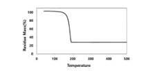
図1に実施例1で製造されたt-ブチルビス(ジメチルアミノ)ヨウ素スズのTGA分析結果を示し、これにより、実施例1のスズ化合物が約110℃で単一蒸発ステップを有することが分かり、500℃で残余物の質量(residue mass)は23.4%と確認されて、迅速な気化を特徴として気化することが分かる。このような結果として、実施例1のスズ化合物は熱安定性が非常に優れていることが分かる。Figure 1 shows the TGA analysis results of t-butylbis(dimethylamino)tin iodide produced in Example 1, which shows that the tin compound of Example 1 has a single evaporation step at about 110°C, and the residue mass at 500°C is confirmed to be 23.4%, showing that it evaporates with rapid evaporation. As a result, it can be seen that the tin compound of Example 1 has excellent thermal stability.
<実施例2>トリス(ジメチルアミノ)ヨウ素スズの製造
[化学式B]
その後、65℃の温度および0.5Torrの圧力下で精製し、トリス(ジメチルアミノ)ヨウ素スズ(Tris(dimethylamino)iodotin)を2g取得した。Then, it was purified at a temperature of 65°C and a pressure of 0.5 Torr to obtain 2 g of tris(dimethylamino)iodotin.
1H NMR (C6D6) : δ 2.54(s, 18H)1 H NMR (C6 D6 ): δ 2.54 (s, 18H)
図2に実施例2で製造されたトリス(ジメチルアミノ)ヨウ素スズのTGA分析結果を示し、これにより、実施例2のスズ化合物が約120℃で単一蒸発ステップを有することが分かり、500℃で残余物の質量(residue mass)は25.0%と確認されて、迅速な気化を特徴として気化することが分かる。このような結果として、実施例2のスズ化合物が熱安定性が非常に優れていることが分かる。Figure 2 shows the TGA analysis results of tris(dimethylamino)tin iodine prepared in Example 2, which shows that the tin compound of Example 2 has a single evaporation step at about 120°C, and the residue mass at 500°C is confirmed to be 25.0%, showing that it evaporates with rapid evaporation. As a result, it can be seen that the tin compound of Example 2 has excellent thermal stability.
<実施例3>ビス(ジメチルアミノ)ヨウ素アンチモンの製造
[化学式C]
その後、50℃温度および0.26Torrの圧力の下で精製し、トリス(ジメチルアミノ)ヨウ素スズ2gを取得した。Then, it was purified at 50°C and 0.26 Torr pressure to obtain 2 g of tris(dimethylamino)tin iodide.
1H NMR (C6D6) : δ 2.49(s, 12H)1 H NMR (C6 D6 ): δ 2.49 (s, 12H)
図3は実施例3で製造されたビス(ジメチルアミノ)ヨウ素アンチモンのTGA分析結果を示し、これにより、実施例3のアンチモン化合物が約137℃で単一蒸発ステップを有することが分かり、500℃で残余物の質量(residue mass)は28.2%と確認されて、迅速な気化を特徴として気化することが分かる。このような結果として、実施例3のアンチモン化合物は熱安定性が非常に優れていることが分かる。Figure 3 shows the TGA analysis results of bis(dimethylamino)iodine antimony prepared in Example 3, which shows that the antimony compound of Example 3 has a single evaporation step at about 137°C, and the residue mass at 500°C is confirmed to be 28.2%, showing that it evaporates with rapid evaporation. As a result, it can be seen that the antimony compound of Example 3 has excellent thermal stability.
<実施例4>ビス(メチルエチルアミノ)ヨウ素アンチモンの製造
[化学式D]
その後、50℃の温度および0.19Torrの圧力下で精製し、ビス(メチルエチルアミノ)ヨウ素アンチモン2gを取得した。Then, it was refined at a temperature of 50°C and a pressure of 0.19 Torr to obtain 2 g of bis(methylethylamino)antimony iodide.
1H NMR (C6D6) : δ 2.36(q, 4H), δ 2.17(s, 6H), δ 0.94(t, 6H)1H NMR (C6 D6 ): δ 2.36 (q, 4H), δ 2.17 (s, 6H), δ 0.94 (t, 6H)
図4は実施例4で製造されたビス(メチルエチルアミノ)ヨウ素アンチモンのTGA分析結果を示し、これにより、実施例4のアンチモン化合物が約124℃で単一蒸発ステップを有することが分かり、500℃で残余物の質量(residue mass)は25.1%と確認されて、迅速な気化を特徴として気化することが分かる。このような結果として、実施例4のアンチモン化合物は熱安定性が非常に優れていることが分かる。Figure 4 shows the TGA analysis results of bis(methylethylamino)iodine antimony prepared in Example 4, which shows that the antimony compound of Example 4 has a single evaporation step at about 124°C, and the residue mass at 500°C is confirmed to be 25.1%, showing that it evaporates with rapid evaporation. As a result, it can be seen that the antimony compound of Example 4 has excellent thermal stability.
<実施例5>
プラズマ強化原子層蒸着法(Plasma Enhanced Atomic Layer Deposition)によって酸化スズ薄膜を製造した。前駆体としては実施例1で製造されたt-ブチルビス(ジメチルアミノ)ヨウ素スズを使用し、反応ガスは酸素ガスを使用した。 Example 5
A tin oxide thin film was prepared by plasma enhanced atomic layer deposition using t-butylbis(dimethylamino) tin iodide prepared in Example 1 as a precursor and oxygen gas as a reactant gas.
酸化スズ薄膜が形成される基板はシリコン基板を使用し、シリコン基板は蒸着チャンバ内に移送し、下記表1に記載の温度を一定に維持した。A silicon substrate was used as the substrate on which the tin oxide thin film was formed. The silicon substrate was transferred into a deposition chamber and maintained at a constant temperature as shown in Table 1 below.
前駆体が充填されたステンレススチール材質のバブラータイプのキャニスターは、表1に記載の所定の前駆体の蒸気圧になるように温度を維持した。蒸気化した前駆体は、アルゴンガスをキャリアガスとしてチャンバ内に移送され、シリコン基板に吸着された。次に、アルゴンガスを使用してパージ工程を実施した。反応ガスである酸素ガスを下記表1に記載の所定のプラズマパワーを使用して反応工程を実施した。また、反応副生成物を除去するために、アルゴンガスを使用してパージ工程を実施した。上記のような原子層蒸着工程を1周期として、所定周期を繰り返して酸化スズ薄膜を形成しており、詳細な評価条件および結果は表1のとおりである。The temperature of the stainless steel bubbler-type canister filled with the precursor was maintained to achieve the vapor pressure of the specified precursor as shown in Table 1. The vaporized precursor was transported into the chamber using argon gas as a carrier gas and adsorbed onto the silicon substrate. Next, a purging process was performed using argon gas. A reaction process was performed using oxygen gas, a reactive gas, at the specified plasma power as shown in Table 1 below. In addition, a purging process was performed using argon gas to remove reaction by-products. The above-mentioned atomic layer deposition process was considered as one cycle, and a tin oxide thin film was formed by repeating a specified cycle, and the detailed evaluation conditions and results are shown in Table 1.
また、酸化スズ薄膜の組成は、X線光電子分光法により分析されており、炭素と窒素およびヨウ素は検出されず、純粋な酸化スズ薄膜を得ることができることを確認した。The composition of the tin oxide thin film was also analyzed by X-ray photoelectron spectroscopy, and no carbon, nitrogen, or iodine was detected, confirming that a pure tin oxide thin film could be obtained.

<実施例6>
原子層蒸着法(Atomic Layer Deposition)によって酸化スズ薄膜を製造した。前駆体としては実施例1で製造されたt-ブチルビス(ジメチルアミノ)ヨウ素スズを使用し、反応ガスはオゾンガスを使用した。 Example 6
A tin oxide thin film was prepared by atomic layer deposition using t-butylbis(dimethylamino)iodine tin prepared in Example 1 as a precursor and ozone gas as a reactant gas.
酸化スズ薄膜が形成される基板はシリコン基板を使用し、シリコン基板は蒸着チャンバ内に移送して下記表2に記載の所定温度に維持した。A silicon substrate was used as the substrate on which the tin oxide thin film was formed, and the silicon substrate was transferred into a deposition chamber and maintained at the specified temperature shown in Table 2 below.
前駆体が充填されたステンレススチール材質のバブラータイプのキャニスターは、下記表2に記載の所定の前駆体の蒸気圧になるように温度を維持した。蒸気化した前駆体は、アルゴンガスをキャリアガスとしてチャンバ内に移送され、シリコン基板に吸着された。次に、アルゴンガスを使用してパージ工程を実施し、反応ガスであるオゾンガスを使用して反応工程を実施した。また、反応副生成物を除去するために、アルゴンガスを使用してパージ工程を実施した。上記のような原子層蒸着工程を1周期として、所定の周期を繰り返して酸化スズ薄膜を形成しており、詳細な評価条件および結果は表2のとおりである。The temperature of the stainless steel bubbler-type canister filled with the precursor was maintained to achieve the vapor pressure of the specified precursor as shown in Table 2 below. The vaporized precursor was transferred into the chamber using argon gas as a carrier gas and adsorbed onto the silicon substrate. Next, a purge process was performed using argon gas, and a reaction process was performed using ozone gas, which is a reactive gas. In addition, a purge process was performed using argon gas to remove reaction by-products. The above-mentioned atomic layer deposition process constitutes one cycle, and a tin oxide thin film was formed by repeating a specified cycle. The detailed evaluation conditions and results are shown in Table 2.
また、酸化スズ薄膜の組成はX線光電子分光法により分析されたが、炭素と窒素は検出されず純粋な酸化スズ薄膜を得ることができることを確認した。In addition, the composition of the tin oxide thin film was analyzed by X-ray photoelectron spectroscopy, and no carbon or nitrogen was detected, confirming that a pure tin oxide thin film could be obtained.

<実施例7>
プラズマ強化原子層蒸着法(Plasma Enhanced Atomic Layer Deposition)によってスズ含有薄膜を製造した。前駆体としては実施例1で製造されたt-ブチルビス(ジメチルアミノ)ヨウ素スズを使用し、反応ガスは二酸化炭素ガスを使用した。 Example 7
A tin-containing thin film was prepared by plasma enhanced atomic layer deposition using t-butylbis(dimethylamino)iodine tin prepared in Example 1 as a precursor and carbon dioxide gas as a reactant gas.
スズ含有薄膜が形成される基板はシリコン基板を使用し、シリコン基板は蒸着チャンバ内に移送して下記表3に記載の所定温度に維持した。A silicon substrate was used as the substrate on which the tin-containing thin film was formed, and the silicon substrate was transferred into a deposition chamber and maintained at the specified temperature shown in Table 3 below.
前駆体が充填されたステンレススチール材質のバブラータイプのキャニスターは、下記表3に記載の所定の前駆体の蒸気圧になるように温度を維持した。蒸気化した前駆体は、アルゴンガスをキャリアガスとしてチャンバ内に移送され、シリコン基板に吸着された。次に、アルゴンガスを使用してパージ工程を実施した。反応ガスである二酸化炭素ガスを下記表3に記載の所定のプラズマパワーを使用して反応工程を実施した。また、反応副生成物を除去するために、アルゴンガスを使用してパージ工程を実施した。上記のような原子層蒸着工程を1周期として、所定の周期を繰り返して酸化スズ含有薄膜を形成しており、詳細な評価条件および結果は表3のとおりである。The temperature of the stainless steel bubbler-type canister filled with the precursor was maintained to achieve the vapor pressure of the specified precursor as shown in Table 3 below. The vaporized precursor was transported into the chamber using argon gas as a carrier gas and adsorbed onto the silicon substrate. Next, a purging process was carried out using argon gas. A reaction process was carried out using carbon dioxide gas, which is a reactive gas, at the specified plasma power as shown in Table 3 below. In addition, a purging process was carried out using argon gas to remove reaction by-products. The above-mentioned atomic layer deposition process was counted as one cycle, and a tin oxide-containing thin film was formed by repeating the specified cycles. The detailed evaluation conditions and results are shown in Table 3.
また、スズ含有薄膜の組成は、X線光電子分光法により分析されており、炭素およびヨウ素が各5~10%含有された薄膜として確認された。The composition of the tin-containing thin film was also analyzed using X-ray photoelectron spectroscopy, and was confirmed to contain 5-10% each of carbon and iodine.

<実施例8>
化学気相蒸着法(Chemical Vapor Deposition)によってスズ含有薄膜を製造した。前駆体としては実施例1で製造されたt-ブチルビス(ジメチルアミノ)ヨウ素スズを使用し、反応ガスは水蒸気を使用した。 Example 8
A tin-containing thin film was prepared by chemical vapor deposition using t-butylbis(dimethylamino)iodine tin prepared in Example 1 as a precursor and water vapor as a reactant gas.
スズ含有薄膜が形成される基板はシリコン基板を使用し、シリコン基板は蒸着チャンバ内に移送して下記表4に記載の所定温度に維持した。A silicon substrate was used as the substrate on which the tin-containing thin film was formed, and the silicon substrate was transferred into a deposition chamber and maintained at the specified temperature shown in Table 4 below.
前駆体が充填されたステンレススチール材質のバブラータイプのキャニスターは、下記表4に記載の所定の前駆体の蒸気圧になるように温度を維持した。蒸気化した前駆体は、アルゴンガスをキャリアガスとしてチャンバ内に移送された。また、反応ガスである水蒸気は水が充填されたステンレススチール材質のバブラータイプのキャニスターを下記表4に記載の所定の蒸気圧になるように温度を維持し、アルゴンガスをキャリアガスとしてチャンバ内に移送した。また、工程圧力は、スロットルバルブを用いてチャンバの圧力が一定に維持されるように調節した。このように、前記前駆体と水蒸気を用いて化学気相蒸着方法を行ってスズ含有薄膜を形成しており、詳細な評価条件および結果は表4のとおりである。The temperature of the bubbler-type canister made of stainless steel filled with the precursor was maintained to reach the vapor pressure of the specified precursor as shown in Table 4 below. The vaporized precursor was transferred into the chamber using argon gas as a carrier gas. In addition, the temperature of the bubbler-type canister made of stainless steel filled with water was maintained to reach the vapor pressure as shown in Table 4 below, and water vapor, which is the reaction gas, was transferred into the chamber using argon gas as a carrier gas. In addition, the process pressure was adjusted using a throttle valve so that the chamber pressure was kept constant. In this way, a chemical vapor deposition method was performed using the precursor and water vapor to form a tin-containing thin film, and detailed evaluation conditions and results are shown in Table 4.
また、スズ含有薄膜の組成は、X線光電子分光法により分析されており、炭素とヨウ素が各5~10%含有された薄膜として確認された。In addition, the composition of the tin-containing thin film was analyzed using X-ray photoelectron spectroscopy, and it was confirmed to contain 5-10% each of carbon and iodine.

<実施例9>
実施例7で製造したスズ含有薄膜を用いて、スズ含有薄膜のパターニングを実施した。 <Example 9>
Using the tin-containing thin film produced in Example 7, patterning of the tin-containing thin film was carried out.
24nmのピッチで1:1ライン-空間ピッチャーを形成するために、極紫外線(EUV、extreme ultraviolet)リソグラフィ装置で約76mJ/cm2の露出でEUVを使用してパターニングした。次いで、3分間約150℃で焼成し、2-ヘプタノンで約15秒間現像した後、同じ溶媒でリンシングをした。 The film was patterned using extreme ultraviolet (EUV) lithography with an exposure of about 76 mJ/cm2 to form 1:1 line-space pitchers with a pitch of 24 nm, then baked at about 150°C for 3 minutes, developed in 2-heptanone for about 15 seconds, and rinsed in the same solvent.
図5は24nmのピッチでシリコン基板上に形成されたライン/空間パターンの走査電子顕微鏡のイメージである。Figure 5 is a scanning electron microscope image of a line/space pattern formed on a silicon substrate with a pitch of 24 nm.
パターンのイメージに示されているように、24nmの狭いピッチでも1:1のライン/空間パターンが均一に形成されたことを確認することができる。As shown in the pattern image, it can be seen that a 1:1 line/space pattern was formed uniformly even with a narrow pitch of 24 nm.
<実施例10>
プラズマ強化原子層蒸着法(Plasma Enhanced Atomic Layer Deposition)によって酸化アンチモン薄膜を製造した。前駆体としては実施例4で製造されたビス(メチルエチルアミノ)ヨウ素アンチモンを使用し、反応ガスは酸素ガスを使用した。 Example 10
An antimony oxide thin film was prepared by plasma enhanced atomic layer deposition using bis(methylethylamino)iodoantimony prepared in Example 4 as a precursor and oxygen gas as a reactant gas.
酸化アンチモン薄膜が形成される基板はシリコン基板を使用し、シリコン基板は蒸着チャンバ内に移送して下記表5に記載の温度に一定に維持した。A silicon substrate was used as the substrate on which the antimony oxide thin film was formed, and the silicon substrate was transferred into a deposition chamber and maintained at a constant temperature as shown in Table 5 below.
前駆体が充填されたステンレススチール材質のバブラータイプのキャニスターは、表5に記載の所定の前駆体の蒸気圧になるように温度を維持した。蒸気化した前駆体は、アルゴンガスをキャリアガスとしてチャンバ内に移送され、シリコン基板に吸着された。次に、アルゴンガスを使用してパージ工程を実施した。反応ガスである酸素ガスを下記表5に記載の所定のプラズマパワーを使用して反応工程を実施した。また、反応副生成物を除去するために、アルゴンガスを使用してパージ工程を実施した。上記のような原子層蒸着工程を1周期として、所定の周期を繰り返して酸化アンチモン薄膜を形成しており、詳細な評価条件および結果は表5のとおりである。The temperature of the stainless steel bubbler-type canister filled with the precursor was maintained to achieve the vapor pressure of the specified precursor as shown in Table 5. The vaporized precursor was transported into the chamber using argon gas as a carrier gas and adsorbed onto the silicon substrate. Next, a purging process was performed using argon gas. A reaction process was performed using oxygen gas, which is a reactive gas, at the specified plasma power as shown in Table 5 below. In addition, a purging process was performed using argon gas to remove reaction by-products. The above-mentioned atomic layer deposition process was considered as one cycle, and a specified cycle was repeated to form an antimony oxide thin film. The detailed evaluation conditions and results are shown in Table 5.
また、酸化アンチモン薄膜の組成は、X線光電子分光法により分析されており、炭素と窒素およびヨウ素は検出されず、純粋な酸化アンチモン薄膜を得ることができることを確認した。The composition of the antimony oxide thin film was also analyzed by X-ray photoelectron spectroscopy, and no carbon, nitrogen, or iodine was detected, confirming that a pure antimony oxide thin film could be obtained.

<実施例11>
原子層蒸着法(Atomic Layer Deposition)によって酸化アンチモン薄膜を製造した。前駆体としては実施例4で製造されたビス(メチルエチルアミノ)ヨウ素スズを使用し、反応ガスはオゾンガスを使用した。 Example 11
An antimony oxide thin film was prepared by atomic layer deposition using bis(methylethylamino)iodine tin prepared in Example 4 as a precursor and ozone gas as a reactant gas.
酸化アンチモン薄膜が形成される基板はシリコン基板を使用し、シリコン基板は蒸着チャンバ内に移送して下記表6に記載の所定温度に維持した。A silicon substrate was used as the substrate on which the antimony oxide thin film was formed, and the silicon substrate was transferred into a deposition chamber and maintained at the specified temperature shown in Table 6 below.
前駆体が充填されたステンレススチール材質のバブラータイプのキャニスターは、下記表6に記載の所定の前駆体の蒸気圧になるように温度を維持した。蒸気化した前駆体は、アルゴンガスをキャリアガスとしてチャンバ内に移送され、シリコン基板に吸着された。次に、アルゴンガスを使用してパージ工程を実施し、反応ガスであるオゾンガスを使用して反応工程を実施した。また、反応副生成物を除去するために、アルゴンガスを使用してパージ工程を実施した。上記のような原子層蒸着工程を1周期として、所定の周期を繰り返して酸化アンチモン薄膜を形成しており、詳細な評価条件および結果は表6のとおりである。The temperature of the stainless steel bubbler-type canister filled with the precursor was maintained to achieve the vapor pressure of the specified precursor as shown in Table 6 below. The vaporized precursor was transferred into the chamber using argon gas as a carrier gas and adsorbed onto the silicon substrate. Next, a purge process was performed using argon gas, and a reaction process was performed using ozone gas, which is a reactive gas. In addition, a purge process was performed using argon gas to remove reaction by-products. The above-mentioned atomic layer deposition process was counted as one cycle, and a specified cycle was repeated to form an antimony oxide thin film. The detailed evaluation conditions and results are shown in Table 6.
また、酸化アンチモン薄膜の組成は、X線光電子分光法により分析されており、炭素と窒素は検出されず、純粋な酸化アンチモン薄膜を得ることができることを確認した。The composition of the antimony oxide thin film was also analyzed using X-ray photoelectron spectroscopy, and no carbon or nitrogen was detected, confirming that a pure antimony oxide thin film could be obtained.

以上、一実施形態を実施例および実験例により詳細に説明しているが、一実施形態の範囲は、特定の実施例に限定されるものではなく、添付の特許請求の範囲によって解釈すべきである。
Although one embodiment has been described in detail above by way of examples and experimental examples, the scope of one embodiment should not be limited to the specific examples, but should be interpreted by the scope of the appended claims.
Claims (10)
Translated fromJapanese[化学式1]

Mは、Sn、Pb、SbまたはBiであり、
R1は、水素またはC1-7アルキルであり、
R2は、C1-7アルキルであり、
R3およびR4は、それぞれ独立して、C1-7アルキル、C2-7アルケニルまたは-NR5R6であり、前記R5およびR6は、それぞれ独立して、水素またはC1-7アルキルであり、
Mの金属酸化数に応じて、前記R3およびR4は、それぞれ独立して存在しなくてもよい。A composition for depositing a metal-containing thin film comprising an iodine-containing metal compound represented by the following formula 1:
[Chemical Formula 1]
M is Sn, Pb, Sb or Bi;
R1 is hydrogen or C1-7 alkyl;
R2 isC1-7 alkyl;
R3 and R4 are each independently C1-7 alkyl, C2-7 alkenyl, or -NR5 R6 , wherein R5 and R6 are each independently hydrogen or C1-7 alkyl;
Depending on the metal oxidation number of M,R3 andR4 may each independently be absent.
前記R3およびR4は、それぞれ独立して、C1-5アルキル、C2-5アルケニルまたは-NR5R6であり、前記R5およびR6は、それぞれ独立して、水素またはC1-5アルキルであり、
Mの金属酸化数に応じて、前記R3およびR4は、それぞれ独立して存在しなくてもよい、請求項1に記載の金属含有薄膜蒸着用組成物。 R1 and R2 each independently represent C1-5 alkyl;
R3 and R4 are each independently a C1-5 alkyl, a C2-5 alkenyl, or -NR5 R6 , and R5 and R6 are each independently a hydrogen or a C1-5 alkyl;
The composition for deposition of a metal-containing thin film according to claim 1 , wherein R3 and R4 may each independently be absent depending on the metal oxidation number of M.
[化学式2]

M1は、SnまたはPbであり、
R11は、水素またはC1-7アルキルであり、
R12は、C1-7アルキルであり、
R13およびR14は、それぞれ独立して、C1-7アルキル、C2-7アルケニルまたは-NR15R16であり、前記R15およびR16は、それぞれ独立して、水素またはC1-7アルキルであってもよい。
[化学式3]

M2は、SbまたはBiであり、
R21は、水素またはC1-7アルキルであり、
R22は、C1-7アルキルであり、
R23は、C1-7アルキル、C2-7アルケニルまたは-NR25R26であり、前記R25およびR26は、それぞれ独立して、水素またはC1-7アルキルであってもよい。 The compositionfor depositing a metal-containing thin film according to claim 1 , wherein the iodine-containing metal compound is represented by the following Formula 2 or 3:
[Chemical Formula 2]
M1 is Sn or Pb;
R11 is hydrogen or C1-7 alkyl;
R12 is C1-7 alkyl;
R13 and R14 are each independently C1-7 alkyl, C2-7 alkenyl or -NR15 R16 , wherein R15 and R16 may each independently be hydrogen or C1-7 alkyl.
[Chemical Formula 3]
M2 is Sb or Bi;
R21 is hydrogen or C1-7 alkyl;
R22 is C1-7 alkyl;
R23 is C1-7 alkyl, C2-7 alkenyl or —NR25 R26 , wherein R25 and R26 may each independently be hydrogen or C1-7 alkyl.
前記R13、R14およびR23は、それぞれ独立して、C1-5アルキルまたはC2-5アルケニルであるか、または前記R15、R16、R25およびR26がそれぞれ独立して、水素またはC1-5アルキルである、請求項3に記載の金属含有薄膜蒸着用組成物。 wherein R11 , R12 , R21 and R22 are each independently a C1-5 alkyl group;
The composition for depositing a metal-containing thin film according to claim 3, wherein R13 , R14 and R23 are each independently a C1-5 alkyl or a C2-5 alkenyl, or R15 , R16 , R25 and R26 are eachindependently a hydrogen or a C 1-5 alkyl .


チャンバ内に装着された基板の温度を30℃~400℃に維持するステップ;
基板上に前記ヨウ素含有金属化合物またはこれを含む金属含有薄膜蒸着用組成物を接触させて前記基板上に吸着させるステップ;および
前記ヨウ素含有金属化合物が吸着された基板に反応ガスを注入して金属含有薄膜を形成させるステップ。 The method for producing a metal-containing thin film according to claim8 , comprising the steps of:
maintaining a temperature of a substrate mounted within the chamber between 30° C. and 400° C.;
A step of contacting the iodine-containing metal compound or a composition for depositing a metal-containing thin film containing the same on a substrate to adsorb it on the substrate; and A step of injecting a reaction gas into the substrate on which the iodine-containing metal compound is adsorbed to form a metal-containing thin film.
Priority Applications (1)
| Application Number | Priority Date | Filing Date | Title |
|---|---|---|---|
| JP2024189001AJP2025003673A (en) | 2022-02-08 | 2024-10-28 | Iodine-containing metal compound and composition for thin film deposition containing the same |
Applications Claiming Priority (4)
| Application Number | Priority Date | Filing Date | Title |
|---|---|---|---|
| KR20220016153 | 2022-02-08 | ||
| KR10-2022-0016153 | 2022-02-08 | ||
| KR1020230009308AKR102822581B1 (en) | 2022-02-08 | 2023-01-25 | Iodine-containing metal compound and composition for thin film deposition comprising the same |
| KR10-2023-0009308 | 2023-01-25 |
Related Child Applications (1)
| Application Number | Title | Priority Date | Filing Date |
|---|---|---|---|
| JP2024189001ADivisionJP2025003673A (en) | 2022-02-08 | 2024-10-28 | Iodine-containing metal compound and composition for thin film deposition containing the same |
Publications (2)
| Publication Number | Publication Date |
|---|---|
| JP2023115908A JP2023115908A (en) | 2023-08-21 |
| JP7645296B2true JP7645296B2 (en) | 2025-03-13 |
Family
ID=87521631
Family Applications (2)
| Application Number | Title | Priority Date | Filing Date |
|---|---|---|---|
| JP2023016388AActiveJP7645296B2 (en) | 2022-02-08 | 2023-02-06 | Iodine-containing metal compound and composition for thin film deposition containing the same |
| JP2024189001APendingJP2025003673A (en) | 2022-02-08 | 2024-10-28 | Iodine-containing metal compound and composition for thin film deposition containing the same |
Family Applications After (1)
| Application Number | Title | Priority Date | Filing Date |
|---|---|---|---|
| JP2024189001APendingJP2025003673A (en) | 2022-02-08 | 2024-10-28 | Iodine-containing metal compound and composition for thin film deposition containing the same |
Country Status (4)
| Country | Link |
|---|---|
| US (1) | US12384805B2 (en) |
| JP (2) | JP7645296B2 (en) |
| CN (1) | CN116574125B (en) |
| TW (1) | TW202332680A (en) |
Citations (2)
| Publication number | Priority date | Publication date | Assignee | Title |
|---|---|---|---|---|
| US20090162973A1 (en) | 2007-12-21 | 2009-06-25 | Julien Gatineau | Germanium precursors for gst film deposition |
| US20140329357A1 (en) | 2008-02-24 | 2014-11-06 | Entegris, Inc. | Tellurium compounds useful for deposition of tellurium containing materials |
Family Cites Families (7)
| Publication number | Priority date | Publication date | Assignee | Title |
|---|---|---|---|---|
| SG178736A1 (en)* | 2007-10-31 | 2012-03-29 | Advanced Tech Materials | Amorphous ge/te deposition process |
| EP2139041B1 (en)* | 2008-06-24 | 2015-08-19 | LG Display Co., Ltd. | Luminescence display panel and method for fabricating the same |
| KR101726620B1 (en)* | 2008-06-24 | 2017-04-14 | 엘지디스플레이 주식회사 | Luminescence dispaly panel and fabricating method of the same |
| US9701695B1 (en)* | 2015-12-30 | 2017-07-11 | American Air Liquide, Inc. | Synthesis methods for amino(halo)silanes |
| US9777373B2 (en)* | 2015-12-30 | 2017-10-03 | American Air Liquide, Inc. | Amino(iodo)silane precursors for ALD/CVD silicon-containing film applications and methods of using the same |
| KR20180063754A (en)* | 2016-12-02 | 2018-06-12 | 삼성전자주식회사 | Tin compound, method of synthesizing the same, tin precursor compound for ALD, and method of forming tin-containing material layer |
| JP7494805B2 (en) | 2020-06-25 | 2024-06-04 | 信越化学工業株式会社 | Chemically amplified resist material and pattern formation method |
- 2023
- 2023-02-06JPJP2023016388Apatent/JP7645296B2/enactiveActive
- 2023-02-07TWTW112104178Apatent/TW202332680A/enunknown
- 2023-02-07CNCN202310144334.5Apatent/CN116574125B/enactiveActive
- 2023-02-07USUS18/165,870patent/US12384805B2/enactiveActive
- 2024
- 2024-10-28JPJP2024189001Apatent/JP2025003673A/enactivePending
Patent Citations (2)
| Publication number | Priority date | Publication date | Assignee | Title |
|---|---|---|---|---|
| US20090162973A1 (en) | 2007-12-21 | 2009-06-25 | Julien Gatineau | Germanium precursors for gst film deposition |
| US20140329357A1 (en) | 2008-02-24 | 2014-11-06 | Entegris, Inc. | Tellurium compounds useful for deposition of tellurium containing materials |
Non-Patent Citations (1)
| Title |
|---|
| C. C. HSU et al,Synthesis and Studies of Trimethylamine Adducts with Tin(II) Halides,Inorganic Chemistry,米国,ACS Publications,1977年10月01日,Vol. 16, 10,P.2529 - p.2534 |
Also Published As
| Publication number | Publication date |
|---|---|
| CN116574125B (en) | 2025-07-25 |
| US20230250114A1 (en) | 2023-08-10 |
| US12384805B2 (en) | 2025-08-12 |
| JP2023115908A (en) | 2023-08-21 |
| TW202332680A (en) | 2023-08-16 |
| JP2025003673A (en) | 2025-01-09 |
| CN116574125A (en) | 2023-08-11 |
Similar Documents
| Publication | Publication Date | Title |
|---|---|---|
| JP7246929B2 (en) | METAL TRIAMINE COMPOUND, METHOD FOR PRODUCING THE SAME AND COMPOSITION FOR METAL CONTAINING THIN FILM VAPOR CONTAINING THE SAME | |
| TWI850906B (en) | Tin-containing precursors for deposition of tin-containing thin films and their corresponding deposition processes | |
| TWI882307B (en) | Area selective deposition of hfo2 ald on metal, oxide, and nitride using inhibitor | |
| JP7645296B2 (en) | Iodine-containing metal compound and composition for thin film deposition containing the same | |
| KR102822581B1 (en) | Iodine-containing metal compound and composition for thin film deposition comprising the same | |
| JP7738107B2 (en) | Composition for vapor deposition of antimony-containing thin films and method for producing antimony-containing thin films using the same | |
| KR102785094B1 (en) | Composition for depositing antimony-containing thin film and method for manufacturing antimony-containing thin film using the same | |
| KR20250000889A (en) | Composition for depositing antimony-containing thin film and method for manufacturing antimony-containing thin film using the same | |
| TWI849615B (en) | Molybdenum compound, preparation method of the same, composition for depositing molybdenum-containing thin film comprising the same, method for producing molybdenum-containing thin film using the composition and molybdenum-containing thin film | |
| TW202506700A (en) | Composition for depositing antimony-containing thin film and method for manufacturing antimony-containing thin film using the same | |
| JP7742191B2 (en) | Molybdenum compound, method for producing the same, and method for producing thin film containing the same | |
| TWI882239B (en) | Silicon precursors, their use and process for preparing the same | |
| JP7503121B2 (en) | Indium compound, its method of manufacture, composition for vapor deposition of indium-containing thin film, and method of manufacture of indium-containing thin film | |
| JP2024132524A (en) | Aminosilsesquioxane | |
| KR20240170453A (en) | Novel amino alkoxy silyl amine compound, method for manufacturing thereof and silicon-containing composition for depositing thin film comprising the same | |
| CN119753637A (en) | IVB group element precursor and application thereof in film deposition |
Legal Events
| Date | Code | Title | Description |
|---|---|---|---|
| A621 | Written request for application examination | Free format text:JAPANESE INTERMEDIATE CODE: A621 Effective date:20230206 | |
| A977 | Report on retrieval | Free format text:JAPANESE INTERMEDIATE CODE: A971007 Effective date:20240124 | |
| A131 | Notification of reasons for refusal | Free format text:JAPANESE INTERMEDIATE CODE: A131 Effective date:20240227 | |
| A521 | Request for written amendment filed | Free format text:JAPANESE INTERMEDIATE CODE: A523 Effective date:20240520 | |
| A131 | Notification of reasons for refusal | Free format text:JAPANESE INTERMEDIATE CODE: A131 Effective date:20240730 | |
| A521 | Request for written amendment filed | Free format text:JAPANESE INTERMEDIATE CODE: A523 Effective date:20241028 | |
| TRDD | Decision of grant or rejection written | ||
| A01 | Written decision to grant a patent or to grant a registration (utility model) | Free format text:JAPANESE INTERMEDIATE CODE: A01 Effective date:20250204 | |
| A61 | First payment of annual fees (during grant procedure) | Free format text:JAPANESE INTERMEDIATE CODE: A61 Effective date:20250303 | |
| R150 | Certificate of patent or registration of utility model | Ref document number:7645296 Country of ref document:JP Free format text:JAPANESE INTERMEDIATE CODE: R150 |