JP7643869B2 - Laser processing device and laser processing method - Google Patents
Laser processing device and laser processing methodDownload PDFInfo
- Publication number
- JP7643869B2 JP7643869B2JP2020217212AJP2020217212AJP7643869B2JP 7643869 B2JP7643869 B2JP 7643869B2JP 2020217212 AJP2020217212 AJP 2020217212AJP 2020217212 AJP2020217212 AJP 2020217212AJP 7643869 B2JP7643869 B2JP 7643869B2
- Authority
- JP
- Japan
- Prior art keywords
- street
- region
- laser processing
- wafer
- surface layer
- Prior art date
- Legal status (The legal status is an assumption and is not a legal conclusion. Google has not performed a legal analysis and makes no representation as to the accuracy of the status listed.)
- Active
Links
- 238000012545processingMethods0.000titleclaimsdescription64
- 238000003672processing methodMethods0.000titleclaimsdescription34
- 239000002344surface layerSubstances0.000claimsdescription68
- 238000012360testing methodMethods0.000claimsdescription28
- 238000003384imaging methodMethods0.000claimsdescription21
- 230000001678irradiating effectEffects0.000claimsdescription4
- 235000012431wafersNutrition0.000description117
- 239000002184metalSubstances0.000description28
- 239000000758substrateSubstances0.000description17
- 239000004065semiconductorSubstances0.000description16
- 238000004519manufacturing processMethods0.000description15
- 230000003287optical effectEffects0.000description8
- 230000006866deteriorationEffects0.000description6
- 238000003331infrared imagingMethods0.000description6
- 238000007493shaping processMethods0.000description6
- 230000003685thermal hair damageEffects0.000description6
- 230000015572biosynthetic processEffects0.000description4
- 239000010410layerSubstances0.000description4
- 238000003860storageMethods0.000description4
- 238000004891communicationMethods0.000description3
- 238000005259measurementMethods0.000description3
- 238000000034methodMethods0.000description3
- 238000010586diagramMethods0.000description2
- 229910000530Gallium indium arsenideInorganic materials0.000description1
- XUIMIQQOPSSXEZ-UHFFFAOYSA-NSiliconChemical compound[Si]XUIMIQQOPSSXEZ-UHFFFAOYSA-N0.000description1
- 230000002146bilateral effectEffects0.000description1
- 230000015556catabolic processEffects0.000description1
- 239000013078crystalSubstances0.000description1
- 238000005520cutting processMethods0.000description1
- 238000013461designMethods0.000description1
- 238000001514detection methodMethods0.000description1
- 238000006073displacement reactionMethods0.000description1
- 230000000694effectsEffects0.000description1
- 238000009413insulationMethods0.000description1
- 239000000463materialSubstances0.000description1
- 239000011159matrix materialSubstances0.000description1
- 238000010309melting processMethods0.000description1
- 238000012986modificationMethods0.000description1
- 230000004048modificationEffects0.000description1
- 230000000704physical effectEffects0.000description1
- 210000001747pupilAnatomy0.000description1
- 229910052710siliconInorganic materials0.000description1
- 239000010703siliconSubstances0.000description1
- 230000003595spectral effectEffects0.000description1
Images


Classifications
- H—ELECTRICITY
- H01—ELECTRIC ELEMENTS
- H01L—SEMICONDUCTOR DEVICES NOT COVERED BY CLASS H10
- H01L21/00—Processes or apparatus adapted for the manufacture or treatment of semiconductor or solid state devices or of parts thereof
- H01L21/70—Manufacture or treatment of devices consisting of a plurality of solid state components formed in or on a common substrate or of parts thereof; Manufacture of integrated circuit devices or of parts thereof
- H01L21/77—Manufacture or treatment of devices consisting of a plurality of solid state components or integrated circuits formed in, or on, a common substrate
- H01L21/78—Manufacture or treatment of devices consisting of a plurality of solid state components or integrated circuits formed in, or on, a common substrate with subsequent division of the substrate into plural individual devices
- B—PERFORMING OPERATIONS; TRANSPORTING
- B23—MACHINE TOOLS; METAL-WORKING NOT OTHERWISE PROVIDED FOR
- B23K—SOLDERING OR UNSOLDERING; WELDING; CLADDING OR PLATING BY SOLDERING OR WELDING; CUTTING BY APPLYING HEAT LOCALLY, e.g. FLAME CUTTING; WORKING BY LASER BEAM
- B23K26/00—Working by laser beam, e.g. welding, cutting or boring
- B23K26/02—Positioning or observing the workpiece, e.g. with respect to the point of impact; Aligning, aiming or focusing the laser beam
- B23K26/04—Automatically aligning, aiming or focusing the laser beam, e.g. using the back-scattered light
- B23K26/046—Automatically focusing the laser beam
- B23K26/048—Automatically focusing the laser beam by controlling the distance between laser head and workpiece
- B—PERFORMING OPERATIONS; TRANSPORTING
- B23—MACHINE TOOLS; METAL-WORKING NOT OTHERWISE PROVIDED FOR
- B23K—SOLDERING OR UNSOLDERING; WELDING; CLADDING OR PLATING BY SOLDERING OR WELDING; CUTTING BY APPLYING HEAT LOCALLY, e.g. FLAME CUTTING; WORKING BY LASER BEAM
- B23K26/00—Working by laser beam, e.g. welding, cutting or boring
- B23K26/02—Positioning or observing the workpiece, e.g. with respect to the point of impact; Aligning, aiming or focusing the laser beam
- B23K26/06—Shaping the laser beam, e.g. by masks or multi-focusing
- B23K26/064—Shaping the laser beam, e.g. by masks or multi-focusing by means of optical elements, e.g. lenses, mirrors or prisms
- B—PERFORMING OPERATIONS; TRANSPORTING
- B23—MACHINE TOOLS; METAL-WORKING NOT OTHERWISE PROVIDED FOR
- B23K—SOLDERING OR UNSOLDERING; WELDING; CLADDING OR PLATING BY SOLDERING OR WELDING; CUTTING BY APPLYING HEAT LOCALLY, e.g. FLAME CUTTING; WORKING BY LASER BEAM
- B23K26/00—Working by laser beam, e.g. welding, cutting or boring
- B23K26/351—Working by laser beam, e.g. welding, cutting or boring for trimming or tuning of electrical components
- B—PERFORMING OPERATIONS; TRANSPORTING
- B23—MACHINE TOOLS; METAL-WORKING NOT OTHERWISE PROVIDED FOR
- B23K—SOLDERING OR UNSOLDERING; WELDING; CLADDING OR PLATING BY SOLDERING OR WELDING; CUTTING BY APPLYING HEAT LOCALLY, e.g. FLAME CUTTING; WORKING BY LASER BEAM
- B23K26/00—Working by laser beam, e.g. welding, cutting or boring
- B23K26/50—Working by transmitting the laser beam through or within the workpiece
- B23K26/53—Working by transmitting the laser beam through or within the workpiece for modifying or reforming the material inside the workpiece, e.g. for producing break initiation cracks
- H—ELECTRICITY
- H01—ELECTRIC ELEMENTS
- H01L—SEMICONDUCTOR DEVICES NOT COVERED BY CLASS H10
- H01L21/00—Processes or apparatus adapted for the manufacture or treatment of semiconductor or solid state devices or of parts thereof
- H01L21/67—Apparatus specially adapted for handling semiconductor or electric solid state devices during manufacture or treatment thereof; Apparatus specially adapted for handling wafers during manufacture or treatment of semiconductor or electric solid state devices or components ; Apparatus not specifically provided for elsewhere
- H01L21/67005—Apparatus not specifically provided for elsewhere
- H01L21/67011—Apparatus for manufacture or treatment
- H01L21/67092—Apparatus for mechanical treatment
- B—PERFORMING OPERATIONS; TRANSPORTING
- B23—MACHINE TOOLS; METAL-WORKING NOT OTHERWISE PROVIDED FOR
- B23K—SOLDERING OR UNSOLDERING; WELDING; CLADDING OR PLATING BY SOLDERING OR WELDING; CUTTING BY APPLYING HEAT LOCALLY, e.g. FLAME CUTTING; WORKING BY LASER BEAM
- B23K2101/00—Articles made by soldering, welding or cutting
- B23K2101/36—Electric or electronic devices
- B23K2101/40—Semiconductor devices
- H—ELECTRICITY
- H01—ELECTRIC ELEMENTS
- H01L—SEMICONDUCTOR DEVICES NOT COVERED BY CLASS H10
- H01L22/00—Testing or measuring during manufacture or treatment; Reliability measurements, i.e. testing of parts without further processing to modify the parts as such; Structural arrangements therefor
- H01L22/30—Structural arrangements specially adapted for testing or measuring during manufacture or treatment, or specially adapted for reliability measurements
- H01L22/34—Circuits for electrically characterising or monitoring manufacturing processes, e. g. whole test die, wafers filled with test structures, on-board-devices incorporated on each die, process control monitors or pad structures thereof, devices in scribe line
Landscapes
- Engineering & Computer Science (AREA)
- Physics & Mathematics (AREA)
- Optics & Photonics (AREA)
- Plasma & Fusion (AREA)
- Mechanical Engineering (AREA)
- Computer Hardware Design (AREA)
- General Physics & Mathematics (AREA)
- Manufacturing & Machinery (AREA)
- Condensed Matter Physics & Semiconductors (AREA)
- Microelectronics & Electronic Packaging (AREA)
- Power Engineering (AREA)
- Chemical & Material Sciences (AREA)
- Chemical Kinetics & Catalysis (AREA)
- General Chemical & Material Sciences (AREA)
- Oil, Petroleum & Natural Gas (AREA)
- Laser Beam Processing (AREA)
- Dicing (AREA)
Description
Translated fromJapanese本発明は、レーザ加工装置及びレーザ加工方法に関する。The present invention relates to a laser processing device and a laser processing method.
ストリートを介して互いに隣り合うように配置された複数の機能素子を含むウェハでは、絶縁膜(Low-k膜等)及び金属構造物(金属杭、金属パッド等)がストリートの表層に形成されている場合がある。そのような場合に、ストリートを通るラインに沿ってウェハの内部に改質領域を形成し、改質領域から亀裂を伸展させることでウェハを機能素子ごとにチップ化すると、ストリートに沿った部分において膜剥がれが生じる等、チップの品質が劣化することがある。そこで、ウェハを機能素子ごとにチップ化するに際し、ストリートにレーザ光を照射することでストリートの表層を除去するグルービング加工が実施される場合がある(例えば、特許文献1,2参照)。In a wafer containing multiple functional elements arranged adjacent to each other with streets interposed therebetween, insulating films (such as low-k films) and metal structures (such as metal piles and metal pads) may be formed on the surface of the streets. In such cases, if modified regions are formed inside the wafer along lines passing through the streets and cracks are allowed to extend from the modified regions to separate the wafer into chips for each functional element, the quality of the chips may deteriorate, such as film peeling occurring along the streets. Therefore, when separating the wafer into chips for each functional element, a grooving process may be performed in which the street is irradiated with laser light to remove the surface layer of the street (see, for example,
しかし、金属構造物を確実に除去し得る条件でストリートにレーザ光を照射すると、ストリートの表層のうち金属構造物が形成されていない部分に熱ダメージが生じるおそれがある。そのような熱ダメージは、チップの品質を劣化させる原因となる。一方、熱ダメージを確実に抑制し得る条件でストリートにレーザ光を照射すると、金属構造物の一部が残存するおそれがある。そのような金属構造物の残存は、ウェハの完全なチップ化を阻害する原因となる。However, if the laser light is irradiated onto the street under conditions that can reliably remove the metal structures, there is a risk of thermal damage occurring in the portions of the street surface where no metal structures are formed. Such thermal damage can cause a deterioration in the quality of the chip. On the other hand, if the laser light is irradiated onto the street under conditions that can reliably suppress thermal damage, there is a risk that some of the metal structures will remain. Such remaining metal structures will hinder the wafer from being completely chipped.
そこで、本発明は、ウェハを機能素子ごとに確実にチップ化すること、及びチップの品質の劣化を抑制することを可能にするレーザ加工装置及びレーザ加工方法を提供することを目的とする。The present invention aims to provide a laser processing device and a laser processing method that can reliably separate a wafer into chips for each functional element and prevent deterioration of the quality of the chips.
本発明のレーザ加工装置は、ストリートを介して互いに隣り合うように配置された複数の機能素子を含むウェハを支持する支持部と、ストリートにレーザ光を照射する照射部と、ストリートに関する情報に基づいて、ストリートの第1領域ではストリートの表層が除去され、且つストリートの第2領域では表層が残存するように、照射部を制御する制御部と、を備え、ストリートに関する情報は、ストリートを通るラインに沿ってウェハの内部に改質領域が形成された場合に、改質領域から伸展した亀裂が、第1領域ではラインに沿ってストリートに到達せず、第2領域ではラインに沿ってストリートに到達するとの情報を含む。The laser processing device of the present invention includes a support section that supports a wafer including a plurality of functional elements arranged adjacent to each other across the streets, an irradiation section that irradiates the streets with laser light, and a control section that controls the irradiation section based on information about the streets so that the surface layer of the street is removed in a first region of the street and the surface layer remains in a second region of the street, and the information about the streets includes information that when a modified region is formed inside the wafer along a line passing through the street, a crack extending from the modified region does not reach the street along the line in the first region, but reaches the street along the line in the second region.
このレーザ加工装置では、「ストリートを通るラインに沿ってウェハの内部に改質領域が形成された場合に、改質領域から伸展した亀裂が、ラインに沿ってストリートに到達しない」と想定される第1領域では、ストリートの表層が除去され、「ストリートを通るラインに沿ってウェハの内部に改質領域が形成された場合に、改質領域から伸展した亀裂が、ラインに沿ってストリートに到達する」と想定される第2領域では、ストリートの表層が除去されない。これにより、ウェハを機能素子ごとにチップ化するに際し、第1領域及び第2領域において、改質領域から伸展した亀裂をラインに沿ってストリートに到達させることができる。また、少なくとも第2領域に対応する部分に熱ダメージが生じるのを防止することができる。よって、このレーザ加工装置は、ウェハを機能素子ごとに確実にチップ化すること、及びチップの品質の劣化を抑制することを可能にする。In this laser processing device, the surface layer of the street is removed in the first region where it is assumed that "when a modified region is formed inside the wafer along a line passing through the street, a crack extending from the modified region will not reach the street along the line," and the surface layer of the street is not removed in the second region where it is assumed that "when a modified region is formed inside the wafer along a line passing through the street, a crack extending from the modified region will reach the street along the line." This allows cracks extending from the modified region in the first and second regions to reach the street along the line when the wafer is chipped for each functional element. It is also possible to prevent thermal damage from occurring at least in the portion corresponding to the second region. Therefore, this laser processing device makes it possible to reliably chip the wafer for each functional element and to suppress deterioration of the quality of the chips.
本発明のレーザ加工装置では、制御部は、レーザ光がストリートに沿って相対的に移動するように、支持部及び照射部の少なくとも一つを制御し、制御部は、レーザ光が第1領域上を相対的に移動する際にレーザ光の出力がONとなり、且つレーザ光が第2領域上を相対的に移動する際にレーザ光の出力がOFFとなるように、照射部を制御してもよい。これによれば、第1領域では、ストリートの表層を確実に除去し、第2領域では、ストリートの表層を確実に残存させることができる。In the laser processing device of the present invention, the control unit controls at least one of the support unit and the irradiation unit so that the laser light moves relatively along the street, and the control unit may control the irradiation unit so that the output of the laser light is ON when the laser light moves relatively over the first region and the output of the laser light is OFF when the laser light moves relatively over the second region. This makes it possible to reliably remove the surface layer of the street in the first region and to reliably leave the surface layer of the street in the second region.
本発明のレーザ加工装置は、ストリートの画像データを取得する撮像部を更に備え、制御部は、画像データ、及びストリートに関する情報に基づいて、第1領域では表層が除去され、且つ第2領域では表層が残存するように、照射部を制御してもよい。これによれば、第1領域ではストリートの表層を除去し、且つ第2領域ではストリートの表層を残存させるレーザ光の照射を確実に実施することができる。The laser processing device of the present invention may further include an imaging unit that acquires image data of the street, and the control unit may control the irradiation unit based on the image data and information about the street so that the surface layer is removed in the first region and the surface layer remains in the second region. This makes it possible to reliably irradiate the laser light in such a way that the surface layer of the street is removed in the first region and the surface layer of the street remains in the second region.
本発明のレーザ加工装置は、ストリートの高さデータを取得する測距部を更に備え、制御部は、高さデータ、及びストリートに関する情報に基づいて、第1領域では表層が除去され、且つ第2領域では表層が残存するように、照射部を制御してもよい。これによれば、第1領域ではストリートの表層を除去し、且つ第2領域ではストリートの表層を残存させるレーザ光の照射を確実に実施することができる。The laser processing device of the present invention may further include a distance measuring unit that acquires height data of the street, and the control unit may control the irradiation unit based on the height data and information about the street so that the surface layer is removed in the first region and the surface layer remains in the second region. This makes it possible to reliably perform irradiation with laser light that removes the surface layer of the street in the first region and leaves the surface layer of the street in the second region.
本発明のレーザ加工装置では、ストリートに関する情報は、第1領域に到達しない亀裂の先端の位置情報を含んでもよい。これによれば、ストリートの表層が除去された第1領域において、改質領域から伸展した亀裂が、ラインに沿ってストリートに確実に到達するように、第1領域にレーザ光を照射することができる。In the laser processing device of the present invention, the information about the street may include position information about the tip of a crack that does not reach the first region. In this way, in the first region where the surface layer of the street has been removed, the first region can be irradiated with laser light so that the crack that extends from the modified region reliably reaches the street along the line.
本発明のレーザ加工方法は、ストリートを介して互いに隣り合うように配置された複数の機能素子を含むウェハを用意する第1工程と、第1工程の後に、ストリートに関する情報に基づいて、ストリートの第1領域ではストリートの表層が除去され、且つストリートの第2領域では表層が残存するように、ストリートにレーザ光を照射する第2工程と、を備え、ストリートに関する情報は、ストリートを通るラインに沿ってウェハの内部に改質領域が形成された場合に、改質領域から伸展した亀裂が、第1領域ではラインに沿ってストリートに到達せず、第2領域ではラインに沿ってストリートに到達するとの情報を含む。The laser processing method of the present invention includes a first step of preparing a wafer including a plurality of functional elements arranged adjacent to each other via streets, and a second step of irradiating the streets with laser light after the first step, so that the surface layer of the street is removed in a first region of the street and the surface layer remains in a second region of the street based on information about the street, and the information about the street includes information that when a modified region is formed inside the wafer along a line passing through the street, a crack extending from the modified region does not reach the street along the line in the first region, but reaches the street along the line in the second region.
このレーザ加工方法では、「ストリートを通るラインに沿ってウェハの内部に改質領域が形成された場合に、改質領域から伸展した亀裂が、ラインに沿ってストリートに到達しない」と想定される第1領域では、ストリートの表層が除去され、「ストリートを通るラインに沿ってウェハの内部に改質領域が形成された場合に、改質領域から伸展した亀裂が、ラインに沿ってストリートに到達する」と想定される第2領域では、ストリートの表層が除去されない。これにより、ウェハを機能素子ごとにチップ化するに際し、第1領域及び第2領域において、改質領域から伸展した亀裂をラインに沿ってストリートに到達させることができる。また、少なくとも第2領域に対応する部分に熱ダメージが生じるのを防止することができる。よって、このレーザ加工方法は、ウェハを機能素子ごとに確実にチップ化すること、及びチップの品質の劣化を抑制することを可能にする。In this laser processing method, the surface layer of the street is removed in the first region where it is assumed that "when a modified region is formed inside the wafer along a line passing through the street, a crack extending from the modified region will not reach the street along the line," and the surface layer of the street is not removed in the second region where it is assumed that "when a modified region is formed inside the wafer along a line passing through the street, a crack extending from the modified region will reach the street along the line." This allows cracks extending from the modified region in the first and second regions to reach the street along the line when the wafer is divided into chips for each functional element. Also, it is possible to prevent thermal damage from occurring at least in the portion corresponding to the second region. Therefore, this laser processing method makes it possible to reliably divide the wafer into chips for each functional element and to suppress deterioration of the quality of the chips.
本発明のレーザ加工方法は、第1工程の前に、テスト用のウェハを用いて、ストリートに関する情報を取得する第3工程を更に備えてもよい。これによれば、ストリートに関する情報を容易に且つ精度良く取得することができる。The laser processing method of the present invention may further include a third step, prior to the first step, of acquiring information about the streets using a test wafer. This makes it possible to easily and accurately acquire information about the streets.
本発明のレーザ加工方法は、第1工程の後に、ラインに沿ってウェハの内部に改質領域を形成する第4工程を更に備えてもよい。これによれば、改質領域から伸展した亀裂をラインに沿ってストリートに到達させることで、ウェハを機能素子ごとにチップ化することができる。The laser processing method of the present invention may further include a fourth step of forming a modified region inside the wafer along the line after the first step. In this way, the wafer can be divided into chips for each functional element by causing cracks extending from the modified region to reach the street along the line.
本発明によれば、ウェハを機能素子ごとに確実にチップ化すること、及びチップの品質の劣化を抑制することを可能にするレーザ加工装置及びレーザ加工方法を提供することができる。The present invention provides a laser processing device and a laser processing method that can reliably separate a wafer into chips for each functional element and suppress deterioration of the quality of the chips.
以下、本発明を実施するための形態について、図面を参照して詳細に説明する。なお、各図において同一又は相当部分には同一符号を付し、重複する説明を省略する。
[レーザ加工装置の構成] Hereinafter, an embodiment of the present invention will be described in detail with reference to the drawings. In each drawing, the same or corresponding parts are denoted by the same reference numerals, and duplicated explanations will be omitted.
[Configuration of laser processing device]
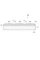
図1に示されるように、レーザ加工装置1は、支持部2と、照射部3と、撮像部4と、制御部5と、を備えている。レーザ加工装置1は、ウェハ20のストリート(詳細については後述する)にレーザ光Lを照射することでウェハ20のストリートの表層を除去するグルービング加工を実施する装置である。以下の説明では、互いに直交する3方向を、それぞれ、X方向、Y方向及びZ方向という。一例として、X方向は第1水平方向であり、Y方向は第1水平方向に垂直な第2水平方向であり、Z方向は鉛直方向である。As shown in FIG. 1, the
支持部2は、ウェハ20を支持する。支持部2は、例えばウェハ20に貼り付けられたフィルム(図示省略)を吸着することで、ストリートを含むウェハ20の表面が照射部3及び撮像部4と向かい合うようにウェハ20を保持する。一例として、支持部2は、X方向及びY方向のそれぞれの方向に沿って移動可能であり、Z方向に平行な軸線を中心線として回転可能である。The
照射部3は、支持部2によって支持されたウェハ20のストリートにレーザ光Lを照射する。照射部3は、光源31と、整形光学系32と、ダイクロイックミラー33と、集光部34と、を含んでいる。光源31は、レーザ光Lを出射する。整形光学系32は、光源31から出射されたレーザ光Lを調整する。一例として、整形光学系32は、レーザ光Lの出力を調整するアッテネータ、レーザ光Lの径を拡大するビームエキスパンダ、レーザ光Lの位相を変調する空間光変調器の少なくとも一つを含んでいる。整形光学系32は、空間光変調器を含む場合、空間光変調器の変調面と集光部34の入射瞳面とが結像関係にある両側テレセントリック光学系を構成する結像光学系を含んでいてもよい。ダイクロイックミラー33は、整形光学系32から出射されたレーザ光Lを反射して集光部34に入射させる。集光部34は、ダイクロイックミラー33によって反射されたレーザ光Lを、支持部2によって支持されたウェハ20のストリートに集光する。The
照射部3は、光源35と、ハーフミラー36と、撮像素子37と、を更に含んでいる。光源35は、可視光V1を出射する。ハーフミラー36は、光源35から出射された可視光V1を反射して集光部34に入射させる。ダイクロイックミラー33は、ハーフミラー36と集光部34との間において可視光V1を透過させる。集光部34は、ハーフミラー36によって反射された可視光V1を、支持部2によって支持されたウェハ20のストリートに集光する。撮像素子37は、ウェハ20のストリートによって反射されて集光部34、ダイクロイックミラー33及びハーフミラー36を透過した可視光V1を検出する。レーザ加工装置1では、制御部5が、撮像素子37による検出結果に基づいて、例えばレーザ光Lの集光点がウェハ20のストリートに位置するように、Z方向に沿って集光部34を移動させる。The
撮像部4は、支持部2によって支持されたウェハ20のストリートの画像データを取得する。撮像部4は、光源41と、ハーフミラー42と、集光部43と、撮像素子44と、を含んでいる。光源41は、可視光V2を出射する。ハーフミラー42は、光源41から出射された可視光V2を反射して集光部43に入射させる。集光部43は、ハーフミラー42によって反射された可視光V2を、支持部2によって支持されたウェハ20のストリートに集光する。撮像素子44は、ウェハ20のストリートによって反射されて集光部43及びハーフミラー42を透過した可視光V2を検出する。The
制御部5は、レーザ加工装置1の各部の動作を制御する。制御部5は、処理部51と、記憶部52と、入力受付部53と、を含んでいる。処理部51は、プロセッサ、メモリ、ストレージ及び通信デバイス等を含むコンピュータ装置である。処理部51では、プロセッサが、メモリ等に読み込まれたソフトウェア(プログラム)を実行し、メモリ及びストレージにおけるデータの読み出し及び書き込み、並びに、通信デバイスによる通信を制御する。記憶部52は、例えばハードディスク等であり、各種データを記憶する。入力受付部53は、オペレータから各種データの入力を受け付けるインターフェース部である。一例として、入力受付部53は、キーボード、マウス、GUI(Graphical User Interface)の少なくとも一つである。
[ウェハの構成] The
[Wafer Configuration]
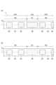
図2及び図3に示されるように、ウェハ20は、半導体基板21と、機能素子層22と、を含んでいる。半導体基板21は、表面21a及び裏面21bを有している。半導体基板21は、例えば、シリコン基板である。半導体基板21には、結晶方位を示すノッチ21cが設けられている。半導体基板21には、ノッチ21cの替わりにオリエンテーションフラットが設けられていてもよい。機能素子層22は、半導体基板21の表面21aに形成されている。機能素子層22は、複数の機能素子22aを含んでいる。複数の機能素子22aは、半導体基板21の表面21aに沿って二次元に配置されている。各機能素子22aは、例えば、フォトダイオード等の受光素子、レーザダイオード等の発光素子、メモリ等の回路素子等である。各機能素子22aは、複数の層がスタックされて3次元的に構成される場合もある。2 and 3, the
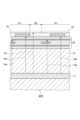
ウェハ20には、複数のストリート23が形成されている。複数のストリート23は、隣り合う機能素子22aの間において外部に露出した領域である。つまり、複数の機能素子22aは、ストリート23を介して互いに隣り合うように配置されている。一例として、複数のストリート23は、マトリックス状に配列された複数の機能素子22aに対して、隣り合う機能素子22aの間を通るように格子状に延在している。図4に示されるように、ストリート23の表層には、絶縁膜24及び複数の金属構造物25,26が形成されている。絶縁膜24は、例えば、Low-k膜である。各金属構造物25,26は、例えば、金属パッドである。金属構造物25と金属構造物26とは、例えば、厚さ、面積、材料の少なくとも一つにおいて、互いに相違している。A plurality of
図2及び図3に示されるように、ウェハ20は、複数のライン15のそれぞれに沿って機能素子22aごとに切断されること(すなわち、機能素子22aごとにチップ化されること)が予定されているものである。各ライン15は、ウェハ20の厚さ方向から見た場合に、各ストリート23を通っている。一例として、各ライン15は、ウェハ20の厚さ方向から見た場合に、各ストリート23の中央を通るように延在している。各ライン15は、レーザ加工装置1によってウェハ20に設定された仮想的なラインである。各ライン15は、ウェハ20に実際に引かれたラインであってもよい。
[レーザ加工装置の動作及びレーザ加工方法] 2 and 3, the
[Operation of laser processing device and laser processing method]
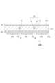
レーザ加工装置1は、各ストリート23にレーザ光Lを照射することで各ストリート23の表層を除去するグルービング加工を実施する。具体的には、支持部2によって支持されたウェハ20の各ストリート23にレーザ光Lが照射されるように、制御部5が照射部3を制御し、レーザ光Lが各ストリート23に沿って相対的に移動するように、制御部5が支持部2を制御する。このとき、制御部5は、図5の(a)に示されるように、レーザ光Lが第1領域R1上を相対的に移動する際にレーザ光Lの出力がONとなり、且つレーザ光Lが第2領域R2上を相対的に移動する際にレーザ光Lの出力がOFFとなるように、照射部3を制御する。ウェハ20では、第1領域R1は、各ストリート23において金属構造物26に対応する領域であり、第2領域R2は、各ストリート23において第1領域R1以外の領域である。The
これにより、図5の(b)に示されるように、各ストリート23の第1領域R1ではストリート23の表層(すなわち、金属構造物26)が除去され、各ストリート23の第2領域R2ではストリート23の表層(すなわち、絶縁膜24及び金属構造物25)が残存させられる。なお、「レーザ光Lが第2領域R2上を相対的に移動する際にレーザ光Lの出力がOFFとなる」とは、厳密には、「仮にレーザ光Lの出力がOFFとならなければ、レーザ光Lが第2領域R2上を相対的に移動するように、ウェハ20に対して照射部3のレーザ光出射部(レーザ加工装置1では、集光部34)が相対的に移動する際に、レーザ光Lの出力がOFFとなる」との意味である。5B, the surface layer of the street 23 (i.e., the metal structure 26) is removed in the first region R1 of each
図6のフローチャートを参照しつつ、レーザ加工装置1を用いたレーザ加工方法について説明する。まず、テスト用のウェハが用意される(図6示されるS01)。テスト用のウェハは、上述したウェハ20と同一の構造を有している。つまり、上述したウェハ20をテスト用のウェハとして用いることができる。以下の説明において区別する必要がある場合には、上述したウェハ20を「量産用のウェハ20」といい、テスト用のウェハを「テスト用のウェハ20A」という。A laser processing method using the
続いて、図7に示されるように、レーザ加工装置(図示省略)において、各ライン15に沿ってテスト用のウェハ20Aにレーザ光L0が照射されることで、各ライン15に沿ってテスト用のウェハ20Aの内部に改質領域11が形成される(図6に示されるS02)。テスト用のウェハ20Aに対する改質領域11の形成条件は、量産用のウェハ20に対する改質領域11の形成条件(詳細については後述する)と同一である。Next, as shown in FIG. 7, in a laser processing device (not shown), laser light L0 is irradiated onto the
一例として、半導体基板21の裏面21bにエキスパンドフィルム12が貼り付けられた状態で、エキスパンドフィルム12を介して半導体基板21の内部にレーザ光L0の集光点が合わされて、テスト用のウェハ20Aにレーザ光L0が照射される。レーザ光L0は、エキスパンドフィルム12及び半導体基板21に対して透過性を有している。半導体基板21の内部にレーザ光L0が集光されると、レーザ光L0の集光点に対応する部分においてレーザ光L0が吸収され、半導体基板21の内部に改質領域11が形成される。改質領域11は、密度、屈折率、機械的強度、その他の物理的特性が周囲の非改質領域とは異なる領域である。改質領域11としては、例えば、溶融処理領域、クラック領域、絶縁破壊領域、屈折率変化領域等がある。改質領域11は、改質領域11からレーザ光L0の入射側及びその反対側に亀裂が延び易いという特性を有している。As an example, with the expand
続いて、エキスパンド装置において、エキスパンドフィルム12が拡張させられることで、各ライン15に沿って半導体基板21の内部に形成された改質領域11からテスト用のウェハ20Aの厚さ方向に亀裂が伸展し、テスト用のウェハ20Aが機能素子22aごとにチップ化される(図6に示されるS03)。Then, in the expansion device, the
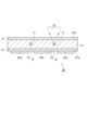
続いて、例えばエキスパンド装置が備える撮像装置において、テスト用のウェハ20Aから得られた複数のチップについて、各ストリート23の画像データが取得され、画像処理装置において、各ストリート23の画像データに基づいて、ストリート23に関する情報が生成される(図6に示されるS04)。各ストリート23の画像が、図8に示される像を含んでいる場合には、ストリート23に関する情報は、「ストリート23を通るライン15に沿ってウェハ20の内部に改質領域11が形成された場合に、改質領域11から伸展した亀裂が、第1領域R1ではライン15に沿ってストリート23に到達せず、第2領域R2ではライン15に沿ってストリート23に到達する」との情報を含むこととなる。以上のように、テスト用のウェハ20Aが用いられて、ストリート23に関する情報が取得される(第3工程)。ストリート23に関する情報は、レーザ加工装置1の制御部5の記憶部52によって記憶される。Next, for example, in an imaging device provided in the expanding device, image data of each
ここで、「改質領域11から伸展した亀裂が、ストリート23を通るライン15に沿ってストリート23に到達する」とは、「改質領域11から伸展した亀裂がストリート23に到達し、且つ切断されたストリート23の両エッジ23aのそれぞれの蛇行が所定幅(ライン15に垂直な方向における所定幅)内に収まっている」との意味である。また、「改質領域11から伸展した亀裂が、ストリート23を通るライン15に沿ってストリート23に到達しない」とは、「改質領域11から伸展した亀裂がストリート23に到達しないか、或いは、改質領域11から伸展した亀裂がストリート23に到達したとしても、切断されたストリート23の両エッジ23aのそれぞれの蛇行が所定幅を超えている」との意味である。所定幅は、例えば、5μm以上20μm以下の値であり、適宜設定される。Here, "the crack extending from the modified
続いて、量産用のウェハ20が用意される(図6示されるS05)(第1工程)。続いて、レーザ加工装置1において、支持部2によって量産用のウェハ20が支持された状態で、撮像部4によって量産用のウェハ20の各ストリート23の画像データが取得される(図6示されるS06)。当該画像データは、レーザ加工装置1の制御部5の記憶部52によって記憶される。続いて、レーザ加工装置1において、量産用のウェハ20に対してグルービング加工が実施される(図6に示されるS07)(第2工程)。Next, mass-
具体的には、支持部2によって支持された量産用のウェハ20の各ストリート23にレーザ光Lが照射されるように、制御部5が照射部3を制御し、レーザ光Lが各ストリート23に沿って相対的に移動するように、制御部5が支持部2を制御する。このとき、制御部5は、撮像部4から取得した各ストリート23の画像データ、及び画像処理装置から取得したストリート23に関する情報に基づいて、図5の(a)及び(b)に示されるように、各ストリート23の第1領域R1ではストリート23の表層が除去され、且つ各ストリート23の第2領域R2ではストリート23の表層が残存するように、照射部3を制御する。Specifically, the
レーザ加工装置1では、制御部5は、撮像部4から取得した各ストリート23の画像データに基づいて、各ストリート23における第1領域R1及び第2領域R2の少なくとも一つの位置情報を予め生成しておき(当該位置情報は、レーザ加工装置1の制御部5の記憶部52によって記憶される)、図5の(a)に示されるように、レーザ光Lが第1領域R1上を相対的に移動する際にレーザ光Lの出力がONとなり、且つレーザ光Lが第2領域R2上を相対的に移動する際にレーザ光Lの出力がOFFとなるように、照射部3を制御する。In the
これにより、図5の(b)に示されるように、各ストリート23の第1領域R1ではストリート23の表層(すなわち、金属構造物26)が除去され、各ストリート23の第2領域R2ではストリート23の表層(すなわち、絶縁膜24及び複数の金属構造物25)が残存させられる。As a result, as shown in FIG. 5B, the surface layer of each street 23 (i.e., the metal structure 26) is removed in the first region R1 of each
続いて、図9に示されるように、レーザ加工装置(図示省略)において、各ライン15に沿って量産用のウェハ20にレーザ光L0が照射されることで、各ライン15に沿って量産用のウェハ20の内部に改質領域11が形成される(図6に示されるS08)(第4工程)。この量産用のウェハ20に対する改質領域11の形成条件(例えば、一本のライン15に対して形成される改質領域11の列数及び位置、各ライン15に沿って改質領域11を形成するためのレーザ光L0の照射条件等)が、テスト用のウェハ20Aに対する改質領域11の形成条件として用いられる。Next, as shown in FIG. 9, in a laser processing device (not shown), the
続いて、図10に示されるように、エキスパンド装置(図示省略)において、エキスパンドフィルム12が拡張させられことで、各ライン15に沿って半導体基板21の内部に形成された改質領域11から量産用のウェハ20の厚さ方向に亀裂が伸展し、量産用のウェハ20が機能素子22aごとにチップ化される(図6に示されるS09)。
[作用及び効果] Next, as shown in FIG. 10, the expand
[Action and Effect]
レーザ加工装置1及びレーザ加工方法(レーザ加工装置1を用いたレーザ加工方法)では、「ストリート23を通るライン15に沿ってウェハ20の内部に改質領域11が形成された場合に、改質領域11から伸展した亀裂が、ライン15に沿ってストリート23に到達しない」と想定される第1領域R1では、ストリート23の表層が除去され、「ストリート23を通るライン15に沿ってウェハ20の内部に改質領域11が形成された場合に、改質領域11から伸展した亀裂が、ライン15に沿ってストリート23に到達する」と想定される第2領域R2では、ストリート23の表層が除去されない。これにより、ウェハ20を機能素子22aごとにチップ化するに際し、第1領域R1及び第2領域R2において、改質領域11から伸展した亀裂をライン15に沿ってストリート23に到達させることができる。また、少なくとも第2領域R2に対応する部分に熱ダメージが生じるのを防止することができる。よって、レーザ加工装置1、及びレーザ加工装置1を用いたレーザ加工方法は、ウェハ20を機能素子22aごとに確実にチップ化すること、及びチップの品質の劣化を抑制することを可能にする。In the
レーザ加工装置1及びレーザ加工方法では、制御部5が、レーザ光Lがストリート23に沿って相対的に移動するように、支持部2を制御し、制御部5が、レーザ光Lが第1領域R1上を相対的に移動する際にレーザ光Lの出力がONとなり、且つレーザ光Lが第2領域R2上を相対的に移動する際にレーザ光Lの出力がOFFとなるように、照射部3を制御する。これにより、第1領域R1では、ストリート23の表層を確実に除去し、第2領域R2では、ストリート23の表層を確実に残存させることができる。In the
レーザ加工装置1及びレーザ加工方法では、撮像部4が、ストリート23の画像データを取得し、制御部5が、ストリート23の画像データ、及びストリート23に関する情報に基づいて、第1領域R1ではストリート23の表層が除去され、且つ第2領域R2ではストリート23の表層が残存するように、照射部3を制御する。これにより、第1領域R1ではストリート23の表層を除去し、且つ第2領域R2ではストリート23の表層を残存させるレーザ光Lの照射を確実に実施することができる。In the
レーザ加工方法では、テスト用のウェハ20Aが用いられて、ストリート23に関する情報が取得される。これにより、ストリート23に関する情報を容易に且つ精度良く取得することができる。In the laser processing method, a
レーザ加工方法では、量産用のウェハ20に対してグルービング加工が実施された後に、各ライン15に沿って量産用のウェハ20の内部に改質領域11が形成される。これにより、改質領域11から伸展した亀裂を各ライン15に沿ってストリート23に到達させることで、量産用のウェハ20を機能素子22aごとにチップ化することができる。
[変形例] In the laser processing method, after grooving is performed on the mass-produced
[Modification]
本発明は、上述した実施形態に限定されない。例えば、ストリート23に関する情報において、「ストリート23を通るライン15に沿ってウェハ20の内部に改質領域11が形成された場合に、改質領域11から伸展した亀裂が、ライン15に沿ってストリート23に到達しない」とされた第1領域R1についての情報は、複数種類の第1領域R1についての情報に細分化されてもよい。その場合には、第1領域R1の種類ごとにレーザ光Lの照射条件が変えられてもよい。The present invention is not limited to the above-described embodiment. For example, in the information regarding the
一例として、図11に示されるように、ストリート23の表層に、絶縁膜24及び複数の金属構造物27,28が形成されている場合において、第1領域R1aが金属構造物27に対応する領域とされ、且つ第1領域R1bが金属構造物28に対応する領域とされ、且つ第2領域R2が金属構造物27,28以外の領域とされたときに、次のように、第1領域R1aと第1領域R1bとでレーザ光Lの照射条件が変えられてもよい。なお、各金属構造物27は、例えば、金属パッドであり、各金属構造物28は、例えば、金属杭である。As an example, as shown in FIG. 11, when an insulating
まず、制御部5は、図12の(a)に示されるように、レーザ光Lが第1領域R1a上を相対的に移動する際にレーザ光Lの出力が第1出力でONとなり、且つレーザ光Lが第1領域R1b上及び第2領域R2上を相対的に移動する際にレーザ光Lの出力がOFFとなるように、照射部3を制御する。続いて、制御部5は、図12の(b)に示されるように、レーザ光Lが第1領域R1b上を相対的に移動する際にレーザ光Lの出力が第2出力(例えば、第1出力よりも低い出力)でONとなり、且つレーザ光Lが第1領域R1a上及び第2領域R2上を相対的に移動する際にレーザ光Lの出力がOFFとなるように、照射部3を制御する。First, the
これにより、図12の(c)に示されるように、ストリート23の第1領域R1a,R1bではストリート23の表層(すなわち、金属構造物27,28)が除去され、ストリート23の第2領域R2ではストリート23の表層(すなわち、絶縁膜24)が残存させられる。なお、レーザ光Lがストリート23に沿って相対的に移動する際に、例えば、整形光学系32に含まれる空間光変調器によって、第1領域R1aと第1領域R1bとで互いに異なるようにレーザ光Lの位相が変調させられてもよい。その場合には、ストリート23に対する一回のレーザ光Lの走査によって、ストリート23の第1領域R1a,R1bにおいてストリート23の表層(すなわち、金属構造物27,28)を除去することができる。12(c), the surface layer of the street 23 (i.e., the
また、ストリート23に関する情報は、第1領域R1に到達しない亀裂の先端の位置情報を含んでいてもよい。一例として、図13に示されるように、ストリート23を通るライン15に沿ってテスト用のウェハ20Aの内部に改質領域11が形成された場合において、第1領域R1では、改質領域11から伸展した亀裂13a,13bがライン15に沿ってストリート23に到達しておらず、第2領域R2では、改質領域11から伸展した亀裂13cがライン15に沿ってストリート23に到達しているときに、ストリート23に関する情報は、各亀裂13a,13bの先端(ストリート23側の先端)の位置情報を含んでいてもよい。これによれば、ストリート23の表層が除去された第1領域R1において、改質領域11から伸展した亀裂13a,13bが、ライン15に沿ってストリート23に確実に到達するように、第1領域R1にレーザ光Lを照射することができる。なお、各亀裂13a,13bの先端は、赤外撮像部によって検出されてもよい。その場合、レーザ加工装置1は、撮像部4に代えて赤外撮像部を備えていてもよいし、撮像部4と共に赤外撮像部を備えていてもよい。赤外撮像部は、対象物に対して赤外光を出射し、赤外光による対象物の像を画像データとして取得するカメラである。赤外撮像部としては、例えば、InGaAsカメラを用いることができる。このように、レーザ加工装置1及びレーザ加工方法では、切断後のストリート23の少なくとも表層を撮像した画像や、赤外線を利用した透視画像を利用して、ストリート23の各領域におけるレーザ光Lの照射条件(レーザON/OFF制御、レーザパワー)をコントロールする情報を作成して、その情報に基づいてグルービング加工をコントロールする。The information on the
また、レーザ加工装置1は、図14に示されるように、ストリート23の高さデータを取得する測距部6を更に備えていてもよい。その場合、制御部5は、ストリート23の高さデータ、及びストリート23に関する情報に基づいて、第1領域R1ではストリート23の表層が除去され、且つ第2領域R2ではストリート23の表層が残存するように、照射部3を制御してもよい。測距部6は、ストリート23に対して測距用の光(例えば、レーザ光)を出射し、ストリート23によって反射された測距用の光を検出することで、ストリート23の高さデータを取得するセンサである。測距部6としては、例えば、三角測距タイプ、分光干渉タイプ、マルチカラー共焦点タイプ、単色共焦点タイプ等のレーザ変位計を用いることができる。The
レーザ加工装置1は、撮像部4に代えて測距部6を備えていてもよいし、撮像部4及び上述した赤外撮像部の少なくとも一つと共に測距部6を備えていてもよい。図15のフローチャートを参照しつつ、図14に示されるレーザ加工装置1を用いたレーザ加工方法について説明する。The
まず、テスト用のウェハ20Aが用意される(図15示されるS11)。続いて、レーザ加工装置において、各ライン15に沿ってテスト用のウェハ20Aにレーザ光L0が照射されることで、各ライン15に沿ってテスト用のウェハ20Aの内部に改質領域11が形成される(図15に示されるS12)。テスト用のウェハ20Aに対する改質領域11の形成条件は、量産用のウェハ20に対する改質領域11の形成条件と同一である。続いて、エキスパンド装置において、エキスパンドフィルム12が拡張させられることで、各ライン15に沿って半導体基板21の内部に形成された改質領域11からテスト用のウェハ20Aの厚さ方向に亀裂が伸展し、テスト用のウェハ20Aが機能素子22aごとにチップ化される(図15に示されるS13)。First, a
続いて、例えばエキスパンド装置が備える撮像装置において、テスト用のウェハ20Aから得られた複数のチップについて、各ストリート23の画像データが取得され、画像処理装置において、各ストリート23の画像データに基づいて、ストリート23に関する情報が生成される(図15に示されるS14)。以上のように、テスト用のウェハ20Aが用いられて、ストリート23に関する情報が取得される(第3工程)。ストリート23に関する情報は、図14に示されるレーザ加工装置1の制御部5の記憶部52によって記憶される。Next, for example, in an imaging device provided in the expanding device, image data of each
続いて、量産用のウェハ20が用意される(図15示されるS15)(第1工程)。続いて、図14に示されるレーザ加工装置1において、測距部6によってストリート23の高さデータが取得されつつ、量産用のウェハ20に対してグルービング加工が実施される(図15に示されるS16)(第2工程)。Next, mass-produced
具体的には、支持部2によって支持された量産用のウェハ20の各ストリート23にレーザ光Lが照射されるように、制御部5が照射部3を制御し、レーザ光Lが各ストリート23に沿って相対的に移動するように、制御部5が支持部2を制御する。このとき、ストリート23において、測距部6が集光部34に対して先行させられることで、図16に示されるように、ストリート23の高さデータが取得される。制御部5は、測距部6から取得したストリート23の高さデータ、及び画像処理装置から取得したストリート23に関する情報に基づいて、各ストリート23の第1領域R1ではストリート23の表層が除去され、且つ各ストリート23の第2領域R2ではストリート23の表層が残存するように、照射部3を制御する。Specifically, the
図16に示されるように、絶縁膜24の高さ、金属構造物25の高さ、及び金属構造物26の高さは、互いに相違している。そのため、制御部5は、測距部6から取得したストリート23の高さデータに基づいて、ストリート23における第1領域R1及び第2領域R2の少なくとも一つの位置情報を予め取得することができる。図14に示されるレーザ加工装置1では、制御部5は、ストリート23における第1領域R1及び第2領域R2の少なくとも一つの位置情報に基づいて、集光部34(すなわち、レーザ光L)が第1領域R1上を相対的に移動する際にレーザ光Lの出力がONとなり、且つ集光部34が第2領域R2上を相対的に移動する際にレーザ光Lの出力がOFFとなるように、照射部3を制御する。これにより、各ストリート23の第1領域R1ではストリート23の表層が除去され、各ストリート23の第2領域R2ではストリート23の表層が残存させられる。16, the height of the insulating
続いて、レーザ加工装置において、各ライン15に沿って量産用のウェハ20にレーザ光L0が照射されることで、各ライン15に沿って量産用のウェハ20の内部に改質領域11が形成される(図15に示されるS17)(第4工程)。この量産用のウェハ20に対する改質領域11の形成条件が、テスト用のウェハ20Aに対する改質領域11の形成条件として用いられる。続いて、エキスパンド装置において、エキスパンドフィルム12が拡張させられことで、各ライン15に沿って半導体基板21の内部に形成された改質領域11から量産用のウェハ20の厚さ方向に亀裂が伸展し、量産用のウェハ20が機能素子22aごとにチップ化される(図15に示されるS18)。Then, in the laser processing device, the
以上のように、図14に示されるレーザ加工装置1では、測距部6が、ストリート23の高さデータを取得し、制御部5が、ストリート23の高さデータ、及びストリート23に関する情報に基づいて、第1領域R1ではストリート23の表層が除去され、且つ第2領域R2ではストリート23の表層が残存するように、照射部3を制御する。これにより、第1領域R1ではストリート23の表層を除去し、且つ第2領域R2ではストリート23の表層を残存させるレーザ光Lの照射を確実に実施することができる。As described above, in the
また、制御部5は、ストリート23の画像データ、ストリート23の高さデータ、及び第1領域R1に到達しない亀裂の先端の位置情報の少なくとも一つ、並びに、ストリート23に関する情報に基づいて、各ストリート23の第1領域R1ではストリート23の表層が除去され、且つ各ストリート23の第2領域R2ではストリート23の表層が残存するように、照射部3を制御してもよい。或いは、制御部5は、ストリート23の画像データ、ストリート23の高さデータ、及び第1領域R1に到達しない亀裂の先端の位置情報を用いずに、ストリート23に関する情報に基づいて、各ストリート23の第1領域R1ではストリート23の表層が除去され、且つ各ストリート23の第2領域R2ではストリート23の表層が残存するように、照射部3を制御してもよい。例えば、制御部5にウェハ20の設計データ等が入力されて、制御部5が、各ストリート23における第1領域R1及び第2領域R2の少なくとも一つの位置情報を予め取得している場合には、ストリート23の画像データ、及びストリート23の高さデータを制御部5が用いる必要はない。The
また、制御部5は、ストリート23に関する情報に基づいて、レーザ光Lが第1領域R1上を相対的に移動する際に第1照射条件(ストリート23の表層が除去される照射条件)でレーザ光Lがストリート23に照射され、且つレーザ光Lが第2領域R2上を相対的に移動する際に第2照射条件(ストリート23の表層が残存する照射条件)でレーザ光Lがストリート23に照射されるように、照射部3を制御してもよい。また、制御部5は、ストリート23に対する複数回のレーザ光Lの走査によって、ストリート23の第1領域R1においてストリート23の表層を除去してもよい。また、制御部5は、レーザ光Lが各ストリート23に沿って相対的に移動するように、支持部2のみを制御してもよいし、照射部3のみを制御してもよいし、或いは、支持部2及び照射部3の両方を制御してもよい。The
また、レーザ加工方法では、量産用のウェハ20に対してグルービング加工が実施された後に、各ライン15に沿って量産用のウェハ20の内部に改質領域11が形成されてもよいし、各ライン15に沿って量産用のウェハ20の内部に改質領域11が形成された後に、量産用のウェハ20に対してグルービング加工が実施されてもよい。In addition, in the laser processing method, after grooving is performed on the mass-produced
1…レーザ加工装置、2…支持部、3…照射部、4…撮像部、5…制御部、6…測距部、11…改質領域、15…ライン、20…ウェハ、20A…テスト用のウェハ、22a…機能素子、23…ストリート、L…レーザ光、R1,R1a,R1b…第1領域、R2…第2領域。1...laser processing device, 2...support section, 3...irradiation section, 4...imaging section, 5...control section, 6...distance measuring section, 11...modified area, 15...line, 20...wafer, 20A...test wafer, 22a...functional element, 23...street, L...laser light, R1, R1a, R1b...first area, R2...second area.
Claims (8)
Translated fromJapanese前記ストリートにレーザ光を照射する照射部と、
前記ストリートに関する情報に基づいて、前記ストリートの第1領域では前記ストリートの表層が除去され、且つ前記ストリートの第2領域では前記表層が残存するように、前記照射部を制御する制御部と、を備え、
前記ストリートに関する前記情報は、前記ストリートを通るラインに沿って前記ウェハの内部に改質領域が形成された場合に、前記改質領域から伸展した亀裂が、前記第1領域では前記ラインに沿って前記ストリートに到達せず、前記第2領域では前記ラインに沿って前記ストリートに到達するとの情報を含む、レーザ加工装置。 a support portion for supporting a wafer including a plurality of functional elements arranged adjacent to each other with streets interposed therebetween;
an irradiation unit that irradiates the street with a laser beam;
a control unit that controls the irradiation unit based on information about the street so that a surface layer of the street is removed in a first region of the street and the surface layer remains in a second region of the street,
A laser processing apparatus, wherein the information regarding the street includes information that, when a modified region is formed inside the wafer along a line passing through the street, a crack extending from the modified region does not reach the street along the line in the first region, but reaches the street along the line in the second region.
前記制御部は、前記レーザ光が前記第1領域上を相対的に移動する際に前記レーザ光の出力がONとなり、且つ前記レーザ光が前記第2領域上を相対的に移動する際に前記レーザ光の出力がOFFとなるように、前記照射部を制御する、請求項1に記載のレーザ加工装置。 the control unit controls at least one of the support unit and the irradiation unit so that the laser light moves relatively along the street;
2. The laser processing apparatus according to claim 1, wherein the control unit controls the irradiation unit so that an output of the laser light is turned ON when the laser light moves relatively over the first region, and is turned OFF when the laser light moves relatively over the second region.
前記制御部は、前記画像データ、及び前記ストリートに関する前記情報に基づいて、前記第1領域では前記表層が除去され、且つ前記第2領域では前記表層が残存するように、前記照射部を制御する、請求項1又は2に記載のレーザ加工装置。 An imaging unit for acquiring image data of the street,
3. The laser processing apparatus according to claim 1, wherein the control unit controls the irradiation unit based on the image data and the information regarding the street so that the surface layer is removed in the first region and the surface layer remains in the second region.
前記制御部は、前記高さデータ、及び前記ストリートに関する前記情報に基づいて、前記第1領域では前記表層が除去され、且つ前記第2領域では前記表層が残存するように、前記照射部を制御する、請求項1~3のいずれか一項に記載のレーザ加工装置。 A distance measuring unit for acquiring height data of the street is further provided,
The laser processing apparatus according to any one of claims 1 to 3, wherein the control unit controls the irradiation unit based on the height data and the information regarding the street so that the surface layer is removed in the first region and the surface layer remains in the second region.
前記第1工程の後に、前記ストリートに関する情報に基づいて、前記ストリートの第1領域では前記ストリートの表層が除去され、且つ前記ストリートの第2領域では前記表層が残存するように、前記ストリートにレーザ光を照射する第2工程と、を備え、
前記ストリートに関する前記情報は、前記ストリートを通るラインに沿って前記ウェハの内部に改質領域が形成された場合に、前記改質領域から伸展した亀裂が、前記第1領域では前記ラインに沿って前記ストリートに到達せず、前記第2領域では前記ラインに沿って前記ストリートに到達するとの情報を含む、レーザ加工方法。 A first step of preparing a wafer including a plurality of functional elements arranged adjacent to each other with streets interposed therebetween;
a second step of irradiating the street with a laser beam after the first step based on information about the street so that a surface layer of the street is removed in a first region of the street and the surface layer remains in a second region of the street,
A laser processing method, wherein the information regarding the street includes information that, when a modified region is formed inside the wafer along a line passing through the street, a crack extending from the modified region does not reach the street along the line in the first region, but reaches the street along the line in the second region.
Priority Applications (7)
| Application Number | Priority Date | Filing Date | Title |
|---|---|---|---|
| JP2020217212AJP7643869B2 (en) | 2020-12-25 | 2020-12-25 | Laser processing device and laser processing method |
| DE112021006653.6TDE112021006653T5 (en) | 2020-12-25 | 2021-12-20 | Laser processing device and laser processing method |
| PCT/JP2021/047081WO2022138588A1 (en) | 2020-12-25 | 2021-12-20 | Laser processing device and laser processing method |
| US18/266,842US20240051067A1 (en) | 2020-12-25 | 2021-12-20 | Laser processing device and laser processing method |
| CN202180086377.1ACN116669895A (en) | 2020-12-25 | 2021-12-20 | Laser processing device and laser processing method |
| KR1020237022706AKR20230121082A (en) | 2020-12-25 | 2021-12-20 | Laser processing device and laser processing method |
| TW110148438ATW202243784A (en) | 2020-12-25 | 2021-12-23 | Laser processing device and laser processing method |
Applications Claiming Priority (1)
| Application Number | Priority Date | Filing Date | Title |
|---|---|---|---|
| JP2020217212AJP7643869B2 (en) | 2020-12-25 | 2020-12-25 | Laser processing device and laser processing method |
Publications (2)
| Publication Number | Publication Date |
|---|---|
| JP2022102471A JP2022102471A (en) | 2022-07-07 |
| JP7643869B2true JP7643869B2 (en) | 2025-03-11 |
Family
ID=82159360
Family Applications (1)
| Application Number | Title | Priority Date | Filing Date |
|---|---|---|---|
| JP2020217212AActiveJP7643869B2 (en) | 2020-12-25 | 2020-12-25 | Laser processing device and laser processing method |
Country Status (7)
| Country | Link |
|---|---|
| US (1) | US20240051067A1 (en) |
| JP (1) | JP7643869B2 (en) |
| KR (1) | KR20230121082A (en) |
| CN (1) | CN116669895A (en) |
| DE (1) | DE112021006653T5 (en) |
| TW (1) | TW202243784A (en) |
| WO (1) | WO2022138588A1 (en) |
Families Citing this family (1)
| Publication number | Priority date | Publication date | Assignee | Title |
|---|---|---|---|---|
| JP2025119075A (en) | 2022-06-27 | 2025-08-14 | シャープ株式会社 | UE (User Equipment) and AMF (Access and Mobility Management Function) |
Citations (5)
| Publication number | Priority date | Publication date | Assignee | Title |
|---|---|---|---|---|
| JP2011142329A (en) | 2002-03-12 | 2011-07-21 | Hamamatsu Photonics Kk | Method of manufacturing light emitting element |
| JP2014216556A (en) | 2013-04-26 | 2014-11-17 | 三星ダイヤモンド工業株式会社 | Processing method for substrate with pattern and processing apparatus for substrate with pattern |
| JP2014223677A (en) | 2013-01-28 | 2014-12-04 | エーエスエム・テクノロジー・シンガポール・ピーティーイー・リミテッド | Method of irradiation-basis scribing semiconductor substrate |
| JP2017174941A (en) | 2016-03-23 | 2017-09-28 | 浜松ホトニクス株式会社 | Laser processing method and laser processing apparatus |
| WO2020255944A1 (en) | 2019-06-17 | 2020-12-24 | ローム株式会社 | SiC SEMICONDUCTOR DEVICE, AND MANUFACTURING METHOD THEREFOR |
Family Cites Families (3)
| Publication number | Priority date | Publication date | Assignee | Title |
|---|---|---|---|---|
| JP2007173475A (en) | 2005-12-21 | 2007-07-05 | Disco Abrasive Syst Ltd | Wafer division method |
| JP5240267B2 (en)* | 2010-09-30 | 2013-07-17 | 三星ダイヤモンド工業株式会社 | Laser processing apparatus, workpiece processing method, and workpiece dividing method |
| JP6558973B2 (en) | 2015-06-18 | 2019-08-14 | 株式会社ディスコ | Device chip manufacturing method |
- 2020
- 2020-12-25JPJP2020217212Apatent/JP7643869B2/enactiveActive
- 2021
- 2021-12-20USUS18/266,842patent/US20240051067A1/enactivePending
- 2021-12-20CNCN202180086377.1Apatent/CN116669895A/enactivePending
- 2021-12-20DEDE112021006653.6Tpatent/DE112021006653T5/enactivePending
- 2021-12-20KRKR1020237022706Apatent/KR20230121082A/enactivePending
- 2021-12-20WOPCT/JP2021/047081patent/WO2022138588A1/ennot_activeCeased
- 2021-12-23TWTW110148438Apatent/TW202243784A/enunknown
Patent Citations (5)
| Publication number | Priority date | Publication date | Assignee | Title |
|---|---|---|---|---|
| JP2011142329A (en) | 2002-03-12 | 2011-07-21 | Hamamatsu Photonics Kk | Method of manufacturing light emitting element |
| JP2014223677A (en) | 2013-01-28 | 2014-12-04 | エーエスエム・テクノロジー・シンガポール・ピーティーイー・リミテッド | Method of irradiation-basis scribing semiconductor substrate |
| JP2014216556A (en) | 2013-04-26 | 2014-11-17 | 三星ダイヤモンド工業株式会社 | Processing method for substrate with pattern and processing apparatus for substrate with pattern |
| JP2017174941A (en) | 2016-03-23 | 2017-09-28 | 浜松ホトニクス株式会社 | Laser processing method and laser processing apparatus |
| WO2020255944A1 (en) | 2019-06-17 | 2020-12-24 | ローム株式会社 | SiC SEMICONDUCTOR DEVICE, AND MANUFACTURING METHOD THEREFOR |
Also Published As
| Publication number | Publication date |
|---|---|
| CN116669895A (en) | 2023-08-29 |
| KR20230121082A (en) | 2023-08-17 |
| TW202243784A (en) | 2022-11-16 |
| US20240051067A1 (en) | 2024-02-15 |
| JP2022102471A (en) | 2022-07-07 |
| WO2022138588A1 (en) | 2022-06-30 |
| DE112021006653T5 (en) | 2023-10-26 |
Similar Documents
| Publication | Publication Date | Title |
|---|---|---|
| JP7307534B2 (en) | Laser processing method, semiconductor device manufacturing method and inspection apparatus | |
| KR102450776B1 (en) | Laser processing method, substrate dicing method, and substrate processing apparatus for performing the same | |
| JP7643869B2 (en) | Laser processing device and laser processing method | |
| JP7313128B2 (en) | IMAGING DEVICE, LASER PROCESSING DEVICE, AND IMAGING METHOD | |
| CN118613895A (en) | Laser processing method | |
| US20220331909A1 (en) | Inspection device and inspection method | |
| JP7313127B2 (en) | IMAGING DEVICE, LASER PROCESSING DEVICE, AND IMAGING METHOD | |
| JP7724059B2 (en) | Laser processing method | |
| JP2021048235A (en) | Inspection device and inspection method | |
| JP7171353B2 (en) | Laser processing method, semiconductor device manufacturing method and inspection device | |
| JP7716850B2 (en) | Laser processing device and laser processing method | |
| TWI894414B (en) | Laser processing device and laser processing method | |
| JP7307533B2 (en) | Laser processing method, semiconductor device manufacturing method and inspection device | |
| CN118574697A (en) | Laser processing device and laser processing method | |
| JP7319770B2 (en) | IMAGING DEVICE, LASER PROCESSING DEVICE, AND IMAGING METHOD |
Legal Events
| Date | Code | Title | Description |
|---|---|---|---|
| A621 | Written request for application examination | Free format text:JAPANESE INTERMEDIATE CODE: A621 Effective date:20231211 | |
| TRDD | Decision of grant or rejection written | ||
| A01 | Written decision to grant a patent or to grant a registration (utility model) | Free format text:JAPANESE INTERMEDIATE CODE: A01 Effective date:20250225 | |
| A61 | First payment of annual fees (during grant procedure) | Free format text:JAPANESE INTERMEDIATE CODE: A61 Effective date:20250227 | |
| R150 | Certificate of patent or registration of utility model | Ref document number:7643869 Country of ref document:JP Free format text:JAPANESE INTERMEDIATE CODE: R150 |