JP7643212B2 - Sheet-like sensor and its manufacturing method - Google Patents
Sheet-like sensor and its manufacturing methodDownload PDFInfo
- Publication number
- JP7643212B2 JP7643212B2JP2021109191AJP2021109191AJP7643212B2JP 7643212 B2JP7643212 B2JP 7643212B2JP 2021109191 AJP2021109191 AJP 2021109191AJP 2021109191 AJP2021109191 AJP 2021109191AJP 7643212 B2JP7643212 B2JP 7643212B2
- Authority
- JP
- Japan
- Prior art keywords
- sensor
- sheet
- resistor
- shear
- load
- Prior art date
- Legal status (The legal status is an assumption and is not a legal conclusion. Google has not performed a legal analysis and makes no representation as to the accuracy of the status listed.)
- Active
Links
Images


Landscapes
- Force Measurement Appropriate To Specific Purposes (AREA)
Description
Translated fromJapanese本開示は、シート状センサに関する。This disclosure relates to a sheet-like sensor.
医療や介護の現場にて、対象者のベッドでの状態を感知するための大面積でシート状のセンサが求められている。特に、安価なシート状の触覚センサは広く用いられておらず、印刷技術を用いて簡単に製造可能なシート状の触覚センサが求められている。
触覚は、振動、応力、圧力、温度を単独または複合して検出する器官であり、触覚に模して、振動、応力、圧力、温度をセンシングする手法が知られており、特にシート状のセンサでこれらを測定する手法が知られている。このような手法を用いた触覚センサとして、抵抗体に対して外部刺激による値の変化から荷重を検出する抵抗体センサが知られている。抵抗値変化型のセンサは、構造が簡単であり、印刷での製造も可能であることから低コストであり、触覚センサとして多くの活用例がある。 In medical and nursing care settings, there is a demand for large-area sheet-type sensors to detect the condition of a patient in bed. In particular, inexpensive sheet-type tactile sensors are not widely used, and there is a demand for sheet-type tactile sensors that can be easily manufactured using printing technology.
Touch is an organ that detects vibration, stress, pressure, and temperature, either alone or in combination, and there are known methods of sensing vibration, stress, pressure, and temperature that imitate touch, particularly a method of measuring these using a sheet-shaped sensor. A known tactile sensor that uses such a method is a resistor sensor that detects load from a change in value of a resistor due to an external stimulus. Resistance change type sensors are low-cost because they have a simple structure and can be manufactured by printing, and there are many examples of their use as tactile sensors.
抵抗値変化型のセンサ素子では、センサ媒体の1軸方向(例えば垂直方向のZ軸)に対する荷重を抵抗値変化として検出する。また、XY平面に平行なせん断荷重を検出する場合には、Z軸検出用のセンサ素子をマトリックス状に並べて、隣り合うセンサ素子のそれぞれから検出されるせん断荷重の時間変化からXY平面に平行な方向のせん断動作を検出する。また、XY平面に平行なせん断荷重を検出するための立体構造を構成して、せん断荷重センサを実現している(例えば、特許文献1)。In a resistance change type sensor element, a load in one axial direction of the sensor medium (for example, the vertical Z-axis) is detected as a change in resistance. When detecting a shear load parallel to the XY plane, sensor elements for detecting the Z-axis are arranged in a matrix, and shear motion parallel to the XY plane is detected from the time change in shear load detected by each of the adjacent sensor elements. A shear load sensor has also been realized by configuring a three-dimensional structure for detecting a shear load parallel to the XY plane (for example, Patent Document 1).
従来の抵抗値変化型の触覚センサでXY平面のずり荷重を検出しようとする場合、素子数が増えるとセンサ素子からの配線や制御システムが複雑化するため大面積でシート状の触覚センサの提供を困難にしていた。
また、特許文献1の方法では、検出素子が複雑な構造を持つため、大面積でシート状のXY平面でのせん断荷重変化を検出するセンサを構成することが困難であった。
本開示では、これらの課題を鑑みて、印刷での製造が可能な安価で大面積化が可能なシート状センサを提供する。 When trying to detect shear load in the XY plane using conventional resistance change type tactile sensors, increasing the number of elements makes the wiring from the sensor elements and the control system more complicated, making it difficult to provide a large-area, sheet-like tactile sensor.
Furthermore, in the method of
In view of these problems, the present disclosure provides a sheet-like sensor that can be manufactured by printing at low cost and has a large area.
課題解決のために、本開示の一態様であるシート状センサは、対向する一対のシート状の基材の間に、2以上のセンサ素子が配置され、各センサ素子は、一対の基材のうちの一方の基材に形成されたシート状の第1の抵抗体と、他方の基材に形成されたシート状の第2の抵抗体とが対向配置すると共に、第1の抵抗体と第2の抵抗体とは、第1の抵抗体に対し第2の抵抗体が相対変位可能な状態で接触し、更に、一対の基材間を連結して、各センサ素子における、第1の抵抗体に対する第2の抵抗体の位置決めを行う接合部を有する、ことを要旨とする。In order to solve the problem, the sheet-like sensor according to one aspect of the present disclosure has two or more sensor elements disposed between a pair of opposing sheet-like substrates, and each sensor element has a sheet-like first resistor formed on one of the pair of substrates disposed opposite a sheet-like second resistor formed on the other substrate, the first resistor and the second resistor are in contact with each other in a state in which the second resistor can be displaced relative to the first resistor, and further has a joint that connects the pair of substrates and positions the second resistor relative to the first resistor in each sensor element.
本開示の他の態様であるシート状センサは、主面以外の面が外装部で覆われている一対の基材と、一対の基材の主面同士の間に配置されたセンサ素子と、一対の基材それぞれの外装部の表面から基材に通じるように設けられた孔と、を備え、一対の基材のうちの一方の基材に設けられた孔は、一対の基材のうちの他方の基材に設けられた孔の外形と平面視で重ならない位置に設けられている、ことを要旨とする。The gist of another aspect of the present disclosure is that the sheet-like sensor comprises a pair of substrates whose surfaces other than the main surfaces are covered with exterior parts, a sensor element disposed between the main surfaces of the pair of substrates, and a hole provided so as to connect the surface of the exterior part of each of the pair of substrates to the substrate, and the hole provided in one of the pair of substrates is provided at a position that does not overlap the outer shape of the hole provided in the other of the pair of substrates in a plan view.
また、本開示の態様であるシート状センサの製造方法は、シート状の第1の基材に抵抗体をパターン印刷してシート状の第1の抵抗体を複数形成し、シート状の第2の基材に抵抗体をパターン印刷して、第1の抵抗体と対向可能な位置にそれぞれ第2の抵抗体を形成し、第1の基材又は第2の基材のうちの一方の基材に対し、平面視において、1又は2以上の第1の抵抗体又は1又は2以上の第2の抵抗体を形成する領域の外周を囲むようにして複数の接合部を形成し、各第1の抵抗体と第2の抵抗体とが対向するようにして第1の基材に第2の基材を重ねると共に、接合部を第1の基材又は第2の基材のうちの他方の基材に固着して、第1の基材と第2の基材を連結する、ことを要旨とする。The method for manufacturing a sheet-like sensor according to the present disclosure includes the steps of: printing a pattern of resistors on a sheet-like first substrate to form a plurality of sheet-like first resistors; printing a pattern of resistors on a sheet-like second substrate to form second resistors at positions that can face the first resistors; forming a plurality of junctions on one of the first substrate or the second substrate so as to surround the periphery of an area in which one or more first resistors or one or more second resistors are formed in a plan view; overlapping the second substrate on the first substrate so that each of the first resistors faces the second resistor; and bonding the junctions to the other of the first substrate or the second substrate to connect the first substrate and the second substrate.
本開示の態様によれば、印刷での製造が可能かつ安価な複数のセンサ素子を配置した大面積のシート状センサ及びシート状センサの製造方法を提供する。According to an aspect of the present disclosure, a large-area sheet-like sensor with multiple sensor elements arranged thereon that can be manufactured inexpensively by printing and a method for manufacturing the sheet-like sensor are provided.
次に、本開示に基づく第1実施形態及び第2実施形態について図面を参照しつつ説明する。
各実施形態では、主として、センサに加わるせん断荷重を抵抗値変化として出力する感圧センサを複数平面方向に配置したシート状センサを例にして説明する。各実施形態は、一般的な垂直方向の感圧センサでは検出できない、XY平面の水平面のせん断荷重を検出するずり感圧センサとして動作するシート状センサである。 Next, a first embodiment and a second embodiment based on the present disclosure will be described with reference to the drawings.
In each embodiment, a sheet-like sensor in which multiple pressure-sensitive sensors are arranged in a planar direction and output a shear load applied to the sensor as a change in resistance value will be mainly described as an example. Each embodiment is a sheet-like sensor that operates as a shear pressure-sensitive sensor that detects a shear load in a horizontal plane of an XY plane, which cannot be detected by a general vertical pressure-sensitive sensor.
1.第1実施形態
以下、図1から図9を参照して、本開示の第1実施形態にかかるシート状センサについて説明する。
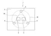
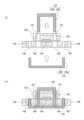
本実施形態にかかるシート状センサは、図1及び図2に示すように、一対の基材2、3の間に複数のセンサ素子4、5と複数の接合部6を配置して構成される。
本実施形態のシート状センサは、図1及び図2に示すように、2つのセンサ素子4、5で1つのセンサの組を構成する場合であって、平面視において、1つのセンサの組を構成する、2つのセンサ素子4、5の外周を囲むようにして、複数(図1では3つ)の接合部6が配置されている例である。センサの組を荷重センサとも呼ぶ。
図1及び図2では、1組の荷重センサだけを図示しているが、一対のシート状の基材2、3間に、複数組の荷重センサが配置されていてもよい。複数組の荷重センサは、平面視において、一対の基材2、3の間にマトリックス状に配置される。1. First Embodiment Hereinafter, a sheet-like sensor according to a first embodiment of the present disclosure will be described with reference to FIGS.
As shown in FIGS. 1 and 2, the sheet-like sensor according to this embodiment is configured by arranging a plurality of
1 and 2, the sheet-like sensor of this embodiment is an example in which two
1 and 2 show only one set of load sensors, multiple sets of load sensors may be disposed between the pair of sheet-
<基材>
シート状の基材2、3は、例えば、熱可塑性プラスチックで形成する。この場合、外部から熱圧を掛けることで、基材2、3同士を複数の接合部6を介して接合できる。基材2、3は、例えば、ポリエチレン、ポリプロピレン、ポリエチレンテレフタレート、ポリカーボネート、アクリルなどのプラスチックフォルムで構成する。
また、基材2、3の表面側(センサ素子を設ける面とは反対側の面)には、ハードコート層を有してものよい。このハードコート層は、例えば、硬化したアクリル層で構成する。このハードコート層の厚さは、例えば1μm以上、5μm以下の範囲とする。この範囲であれば、基材2、3の傷付きを防止しつつ、ハードコート層自体の割れも防止しやすい。<Substrate>
The sheet-
The
更に、基材2、3の内側(対向面側)に接合層を有してもよい。接合層は、例えばウレタン層から構成する。接合層の厚さは、例えば、1μm以上、10μm以下の範囲とする。
また、基材2、3の各厚さは、例えば、25μm以上、200μm以下の範囲とする。この範囲であれば、基材2、3が折れ曲がり難くなり、且つ丸めたりすることができるようになる。また、基材2、3が、センサ素子4、5を構成する抵抗体4A、4B、5A、5Bを担持でき、センサ素子4、5を外部から保護できる。 Furthermore, a bonding layer may be provided on the inside (opposing surface) of the
The thickness of each of the
<センサ素子>
本実施形態では、1つの荷重センサを構成する2つのセンサ素子4、5は、X軸抵抗素子及びY軸抵抗素子である。
X軸抵抗素子及びY軸抵抗素子を構成する各センサ素子4、5は、一対の基材2、3のうちの、一方の基材2に形成されたシート状の第1の抵抗体4A、5Aと、他方の基材3に形成されたシート状の第2の抵抗体4B、5Bとを有する。第1の抵抗体4A、5Aと第2の抵抗体4B、5Bとは、第1の抵抗体4A、5Aに対し第2の抵抗体4B、5Bが面方向(横方向)に相対変位可能な状態で、対向配置されて、第1の抵抗体4A、5Aの抵抗表面4Aa、5Aaと第2の抵抗体4B、5Bの抵抗表面4Ba、5Baが周可能に接触して接触面10を形成している。<Sensor element>
In this embodiment, the two
Each of the
X軸抵抗素子(センサ素子4)は、X軸方向にせん断荷重が発生したときに、第1の抵抗体4Aと第2の抵抗体4Bとの接触面積が変化して、ずり変位に応じ抵抗値が変化する。Y軸抵抗素子(センサ素子5)も同様に、Y軸方向のせん断荷重に対して抵抗値が変化する。なお、X軸とY軸で示す座標系は、直交座標系でなくてもよく、斜交座標系であってもよい。When a shear load is applied in the X-axis direction, the contact area between the
各センサ素子4、5は、対向した2つの抵抗体4A、4B、5A、5Bの接触面積がせん断荷重に対して変化することで、荷重を算出する情報(抵抗値)を出力する。せん断荷重の算出法としては、予め決められたX方向とY方向それぞれ荷重を加えたときの抵抗値を測定して、予め検量線を設定しておく。そして、実際のせん断荷重を計測する場合は、せん断荷重時の接触面10の抵抗値を、検量線に基づきせん断荷重に変換して算出する。Each
ここで、各センサ素子4、5は、第1の抵抗体4A、5Aと第2の抵抗体4B、5Bの接触面10の抵抗値が数Ωから数百Ωになるようにすれば良い。また、センサ素子4、5を形成する抵抗体4A、4B、5A、5Bの各材料の抵抗値は、接触面10の抵抗値を計測するために導電経路となるため、接触面10の抵抗値よりも低い抵抗値を示す材料と寸法の組合せを選択すればよい。
また、接触面10の抵抗値は、表面粗さを調整して、接触面積を増減し抵抗値を調整しても良い。 Here, it is sufficient that the resistance value of the
The resistance value of the
第1の抵抗体4A、5Aと第2の抵抗体4B、5Bは、例えば、導電性を有する樹脂から構成する。導電性を有する樹脂は、バインダー樹脂にカーボンフィラーや金属フィラーが分散した導電インクを基材2、3の表面にパターン印刷又はコーティングして形成できる。また、金属パターン(リード線(配線50~55)のパターン、図8、9参照)の表面に酸化被膜を形成して接触面10の抵抗値を調整しても良い。第1の抵抗体4A、5Aと第2の抵抗体4B、5Bを、パターン印刷で形成した場合、各センサ素子4、5を個別に配列しやすい。印刷方法としては、スクリーン印刷、グラビア印刷、インクジェットなどの手法が挙げられる。また、コーティング手法としては、グラビアコート、静電スプレー、ダイコートなどが挙げられる。コーティング手法では抵抗素子のパターンのマスクを用いて形成する。The
ここで、実際のずり変位を伴うせん断荷重を印加する場合、必ず垂直方向(対向方向)のZ軸荷重が加わった状態でせん断荷重が印加される。また、ずり変位は、せん断荷重に対して抗力として働くZ軸荷重印加の接触面10での摩擦力との差分が、接合部6に作用する際の接合部6の材料の粘弾特性で決まる。このため、せん断荷重の算出の際に、Z軸荷重及び接合部6の材料の粘弾特性で算出値に補正を行うことが好ましい。Z軸荷重は、別途、圧力検知用の上記構成のセンサ素子4、5を追加すればよい。Here, when applying a shear load accompanied by actual shear displacement, the shear load is always applied in the presence of a vertical (opposing) Z-axis load. The shear displacement is determined by the viscoelastic properties of the material of the joint 6 when the difference between the frictional force at the
すなわち、実際のずり変位を伴うせん断荷重を印加する場合、必ず垂直方向(対向方向)のZ軸荷重が加わった状態でせん断荷重が印加される。また、ずり変位は、せん断荷重に対して抗力として働くZ軸荷重印加の接触面10での摩擦力との差分が、接合部6に作用する際の接合部6の材料の粘弾特性で決まる。このため、せん断荷重の算出の際に、Z軸荷重及び接合部6の材料の粘弾特性で算出値に補正を行うことが好ましい。Z軸荷重は、別途、圧力検知用の上記構成のセンサ素子4、5を追加すればよい。すなわち、図には記載していないが、各荷重センサに対し、抵抗値変化型の垂直荷重用のセンサを追加、配置して、荷重センサを、X軸とY軸の検知に加えてZ軸の検知の3軸のセンサとすることもできる。このとき、Z軸荷重から接触面10に作用する摩擦力を補正し、垂直荷重からせん断荷重の検量線を調整してもよい。
また、基材2、3には、センサ素子4、5から抵抗値測定用の引き出し配線(リード線)を配しておく。リード線は、プリント配線板を用いても良いし、銀ペーストなどの導電インクを用いて印刷してもよい。 That is, when applying a shear load accompanied by an actual shear displacement, the shear load is always applied in a state where a Z-axis load in the vertical direction (opposing direction) is applied. In addition, the shear displacement is determined by the viscoelastic properties of the material of the joint 6 when the difference between the frictional force at the
Furthermore, wiring (lead wires) for measuring resistance values are provided from the
<接合部>
接合部6は、各荷重センサに設けられる。接合部6は、対応する荷重センサを構成する複数のセンサ素子4、5の外周に配設され、一対の基材2、3間を連結して、対応する荷重センサを構成する各センサ素子4、5における、上記第1の抵抗体4A、5Aに対す
る上記第2の抵抗体4B、5Bの位置決めを行う。接合部6は、センサ素子4、5のX-Y方向とZ方向の三軸方向の初期位置(無負荷時の位置)を規定する。
図2に示すように、対向する基材2、3は、接合部6でのみ連結されており、X軸抵抗素子4とY軸抵抗素子5は、対向した抵抗体4A、4B、5A、5Bの表面(抵抗表面4Aa、5Aa、4Ba、5Ba)で接触した界面からなる接触面10を有する。<Joint>
The joint 6 is provided on each load sensor. The joint 6 is disposed on the outer periphery of a plurality of
As shown in FIG. 2, the opposing
接合部6は、例えば、ピラー状のパッチで形成するか、一対の基材2、3の片方又は両方の表面に印刷などで形成すればよい。
接合部6の材料を粘着剤や接着剤で形成した後、基材2、3を圧着して接合部6で接合することが可能である。
また、接合部6は、熱可塑材料で形成することも可能であり、この場合は、全面加熱印加するラミネーターなどで熱圧着することで、接合部6を形成する材料が加熱され融着することで、接合部6を介して基材2、3が接合される。
接合部6の他方の形成方法として、前記した基材2、3を熱可塑材料にするか、別途、荷重センサ素子パターンの下層に熱可塑からなる接合層を設け、後から接合部6の位置でパターン化した熱スタンプを押しあてて、接合部6部分のみを加熱接合することで、基材2、3とを接合することも可能である。 The joint 6 may be formed, for example, by a pillar-shaped patch, or may be formed by printing on the surface of one or both of the pair of
After the material of the joint 6 is formed using a pressure sensitive adhesive or adhesive, the
The joint 6 can also be formed from a thermoplastic material. In this case, the material forming the joint 6 is heated and fused by thermocompression using a laminator that applies heat to the entire surface, thereby joining the
As another method for forming the joint 6, the above-mentioned
接合部6の材料としては、例えば、弾性材料の樹脂から選択する。具体的には、接合部6の材料として、ポリエチレン、ポリプロピレン、ポリ塩化ビニル、ポリスチレン、ポリ酢酸ビニル、ポリウレタンなどが例示できる。接合部6は、接合工程時に、熱可塑、熱硬化、UV硬化などにより接着、固化で基材2、3を接合できる材料であれば、材料や接合工程に限定されるものではない。
なお、抵抗体4A、4B、5A、5Bの材料は、接合部6の材料よりも硬い材料の方が、抵抗体4A、4B、5A、5Bの変形が抑えられて好ましい。 The material of the joint 6 is selected from, for example, elastic resins. Specific examples of the material of the joint 6 include polyethylene, polypropylene, polyvinyl chloride, polystyrene, polyvinyl acetate, polyurethane, etc. The material and joining process of the joint 6 are not limited as long as the material can join the
It is preferable that the material of the
接合部6は、センサ素子4、5の厚みに対し厚くても薄くても良い。接合部6の方が厚い場合は、接合部6で囲まれた部分が凹形状になる。接合部6の方が薄い場合は、接合部6で囲まれた部分が凸形状になる。
本実施形態では、以下のように、接合部6が、センサ素子4、5に対して好適に配置されるため、せん断荷重時の接触面10の摩擦が安定することになる。
本実施形態では、荷重センサ毎に、図1に示すように、荷重センサを構成する複数のセンサ素子4、5の外周を囲むようにして、3個以上の接合部6を配置する。 The joint 6 may be thicker or thinner than the thickness of the
In this embodiment, the joint 6 is suitably disposed with respect to the
In this embodiment, as shown in FIG. 1, three or
3個以上の接合部6は、例えば、平面視において、対応するセンサの組を構成する2以上のセンサ素子4、5の質量中心を中心とした第1の円30の円状にそれぞれ配置されると共に、隣り合う接合部6間の距離が等しい位置(等間隔位置)に設けられる。すなわち、第1の円30の中心を中心とした正多角形形状(接合部6の個数と同じ角数とする)の角部位置にそれぞれの接合部6が配置される。このとき、各荷重センサを構成する2以上のセンサ素子4、5は、上記質量中心を中心した第2の円20に内接するように配置され、第1の円30の半径は、第2の円20の半径の2倍以下である、ことが好ましい。The three or
すなわち、本実施形態では、荷重センサとして、Z荷重に対し抵抗体4A、4B、5A、5Bの表面へ平均的に荷重印加させるため、質量中心を中心とした円の内側にセンサ素子4、5を配置し、3点以上の接合部6をセンサ素子4、5中心からセンサ素子4、5に外接する円の半径の1倍以上2倍の円内に配置している。2倍の円内とすることで、確実に対向する抵抗体4A、4B、5A、5B同士が接触可能とできる。接合部6の配置の位置は、センサ素子4、5の質量中心を中心とした正多角形の頂点に位置するように配置することができる。この質量中心は、素子の輪郭の外形のみから求めた疑似的な重心とできる。つまり、素子の輪郭内部は、2次元的に均一の質量の物質と仮定した場合の重心である。この疑似的な重心は、素子に掛かる圧力の中心と一致し、好ましい。センサ素子4、5の質量中心の位置は、組を構成するセンサ素子4、5の質量中心である。接合部6は、センサ素子4、5の外周を周方向に間隔を空けて囲むように、ドットパターンで対向する基材2、3間に形成する。つまり接合部6の形状は、ドットとできる。ドットは、円とできる。また、楕円でもよい。これによって、圧を掛けた際に、抵抗体4A、4B、5A、5Bの接触面10が閉じた空間に封止されることなくエアが抜けるので、接触面10でのエア噛みがなくなり、各センサ素子4、5の接触面10での接触が安定する。このように接合部6を配置することで、シート状センサへの垂直方向のZ軸荷重時に対し、抵抗体4A、4B、5A、5Bの各接触面10が均等化した垂直荷重が加わることになる。荷重時に生じる抵抗体4A、4B、5A、5Bの接触面10の摩擦力がせん断荷重に対して一定の抗力として働くことになり、せん断荷重時の抵抗体4A、4B、5A、5B面積の変化量もせん断荷重に対して一定になる。また、このような構造であれば、荷重センサが振動しがたくなり、2次元平面方向にいずれの方向にも安定して変位可能となる。That is, in this embodiment, in order to apply an even load to the surfaces of the
<センサ素子の構成例>
図3(a)及び図3(b)を用いて、せん断荷重を検出するセンサ素子4、5の構成例について説明する。図3(a)は、センサ素子4の一構成例を示す平面図であり、図3(b)は、センサ素子4の一構成例を示す断面図である。
図3(a)及び図3(b)に示すセンサ素子4では、第1の抵抗体4A及び第2の抵抗体4Bを共に長方形状とするが長辺の長さが異なる形状とした。そして、平面視において、そして、2つの抵抗体4A、4Bの各短辺方向が、せん断検出方向となるように配置して、2つの抵抗体4A、4Bの短辺の一部が重なるように配置した。また長辺方向においては、長辺の短い抵抗体4A、4Bが、長辺が長い抵抗体4A、4Bの中央位置となるように設定した。センサ素子5についても同様な構成となっている。<Example of sensor element configuration>
An example of the configuration of the
In the
なお、第1の抵抗体4A、5A及び第2の抵抗体4B、5Bの形状や配置は、これに限定されない。対向配置された2つの抵抗体4A、4B、5A、5Bが、平面視において、検知するせん断力の方向へのせん断変位に応じて、2つの抵抗体4A、4B、5A、5Bの重なる領域の面積が変化すると共に、検知するせん断力の方向と直交する方向のせん断変位に対し、2つの抵抗体4A、4B、5A、5Bの重なる領域の面積が一定に維持されるように、上記2つの抵抗体4A、4B、5A、5Bの形状及び配置が構成されていればよい。
この場合、第1の抵抗体4A、5Aと第2の抵抗体4B、5Bが、接触面10を介して接続され、接触面10の抵抗値をせん断荷重に変換する。 The shapes and arrangement of the
In this case, the
図3(a)において、X-X′方向をX軸方向(せん断検出方向)とすると、X軸プラス方向(紙面右方向)にせん断荷重に応じてずり変位が発生すると抵抗体4Aと抵抗体4Bの重なり面積が増加し、接触抵抗が低下する。逆にX軸がマイナス方向(紙面左方向)にせん断荷重が印加される場合には重なり面積が低下し、接触抵抗が増加する。X軸のせん断荷重方向で接触抵抗が増加又は低下することで、せん断応力を検出することが可能となっている。一方、縦方向のY軸方向にせん断が発生する場合には、抵抗体4Aが抵抗体4Bの長辺方向端部位置まですり変位しても抵抗体4Aと抵抗体4Bの重なり面積は変化しない。結果として、Y方向のせん断荷重は検出せず、X軸のせん断荷重成分だけを分離して検出可能となっている。Y方向のせん断荷重を検出する場合には、X軸測定用のセンサ素子4に対して90°回転させて配置すれば、同様にY軸のみのせん断荷重を検出することを可能とする。90°配置の異なる2つのセンサ素子4、5を1組として配置することで、XY平面に加わるせん断荷重を全方位で計測が可能とする荷重センサを構成できる。In FIG. 3(a), if the X-X' direction is the X-axis direction (shear detection direction), when shear displacement occurs in the positive X-axis direction (right direction on the paper) in response to a shear load, the overlap area of
図3(a)及び図3(b)に示す構成例を採用した、1組の荷重センサを構成する、各センサ素子4、5の配置例を図4(a)及び図4(b)に示す。
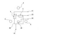
図4(a)に示す荷重センサは、X軸抵抗素子4とY軸抵抗素子5の1セットと、3つの接合部6を正三角形の頂点に配した場合である。また、配置する複数の接合部6は、断面が大きな接合部6と断面が小さな接合部6を有してもよい。大きな接合部6と小さな接合部6の数の比率は、例えば、1:1以上1:6以下とすることできる。また、大きな接合部6の外周に小さな接合部6を配置してもよい。このような配置とすることで、大きな接合部6に掛かる応力を小さな接合部6に分散することができる。また、組を構成するセンサ素子の質量中心を中心として、大きな接合部6の外側に小さな接合部6を配置してもよい。このような配置では、小さな接合部6の一部が破断した際には、荷重センサに周囲の素子値に対して異常値を示すため、完全に破損し動作しなくなる前に、不具合を検知しやすい。 FIGS. 4(a) and 4(b) show examples of the arrangement of the
The load sensor shown in FIG. 4(a) is a case where one set of an X-axis
図4(b)に示す荷重センサは、X軸抵抗素子4とY軸抵抗素子5を2セット有すると共に、4つの接合部6が正四角形の頂点に配された場合である。このような配置関係にすることで、各センサ素子4、5に印加される垂直荷重が平均化し、荷重センサ中の各接触面10への接触面荷重が安定する。この結果、接触面10の摩擦と電気抵抗が安定する。また、上記のように接合部6の配置を設定することで、せん断荷重がXY平面(二次元方向)でいずれの方向から印加された場合でも、センサ素子4、5に偏りなせん断荷重が印加され、より正確なせん断荷重の計測を可能とする。
なお、図4(a)及び図4(b)は、本実施形態の一例を示すものであって、1組の荷重センサを構成するセンサ素子4、5のセット数と接合部6の配置の正多角形の頂点数を限定するものではない。 The load sensor shown in FIG. 4(b) has two sets of X-axis
Note that Figures 4(a) and 4(b) show an example of this embodiment, and do not limit the number of sets of
接合部6を配置する多角形の数量を増やせば、円形に近づくことになり、XYの全方位に対して平均的にせん断荷重をセンサ素子4、5のずり変位として伝える。また、1組の荷重センサを構成するセンサ素子4、5のセット数を増やすことで助長性を向上し正確な計測を可能とする。
また、センサ素子4、5のセットと接合部6からなる荷重センサを、マトリックス状に多数配置し、それぞれの抵抗値を測定することでXY平面に広がるせん断荷重の面積分布を計測することも可能である。 Increasing the number of polygons in which the
It is also possible to measure the areal distribution of the shear load spreading in the XY plane by arranging a large number of load sensors, each consisting of a set of
なお、基材2、3間に複数組の荷重センサをマトリックス状に配置しても良いし、上記記載のように、基材2、3間に1組の荷重センサからなるセンサ部品を複数用意して、他の2次元センサの上にマトリックス状に敷並べてもよい。この場合、他の2次元センサに対し各センサ部品を着脱可能に取り付けることが好ましい。
また、同特性のセンサ素子4、5を多数配置し、複数の素子セットでデータ検出することで、ロバスト性を持たせることも可能である。この場合、一部の素子が故障しても、周囲の素子の値で、故障した素子の値を補完できる。また、多数の素子間での異常から、素子の不具合を検知しやすい。 A plurality of sets of load sensors may be arranged in a matrix between the
It is also possible to provide robustness by arranging
また、複数の荷重センサを一平面に敷き並べた場合には、隣接する荷重センサの素子群の値どうしを整合させることで、容易にインフィールドでのキャリブレーションが行える。これらの異常の検知や、キャリブレーションには、機械学習を用いてもよい。特に複数の荷重センサが配列していることから、機械学習に用いるデータを多く取得できるため、効率的な機械学習が行える。この機械学習は、階層的な機械学習としてもよい。この場合、一点一点の値そのものを教師データとすることもできるし、値の分布のパターンを教師データとすることもできる。また、複数のシートのデータを教師データとすることもできる。複数のシートを用いた場合には、非連続的な値の変化等から、シートが交換されたことやシート自体の異常を検知できる。このように同じ特性の素子を多数配置することで、機械学習による素子の異常や、補完が効果的に行える。In addition, when multiple load sensors are arranged on a single plane, in-field calibration can be easily performed by matching the values of the element groups of adjacent load sensors. Machine learning may be used to detect these abnormalities and perform the calibration. In particular, since multiple load sensors are arranged, a large amount of data to be used for machine learning can be obtained, allowing efficient machine learning. This machine learning may be hierarchical machine learning. In this case, the values of each point themselves can be used as training data, or the pattern of the value distribution can be used as training data. In addition, data from multiple sheets can be used as training data. When multiple sheets are used, it is possible to detect the replacement of the sheets or abnormalities in the sheets themselves from discontinuous changes in values, etc. By arranging a large number of elements with the same characteristics in this way, abnormalities in the elements and complementation by machine learning can be effectively performed.
複数の荷重センサは正方配列や、六方配列としてもよい。また、精度向上や冗長性のため、複数の荷重センサを一つのセルとし配置してもよい。
センサ素子4、5の抵抗値変化を時間で分解し振動検出型の素子としたり、センサ素子4、5を温度可変型の抵抗材料を選択することで温度検出型にしたりすることで、振動検知や温度検知のシート状センサとすることも可能である。 The plurality of load sensors may be arranged in a square or hexagonal array. In addition, for improved accuracy and redundancy, the plurality of load sensors may be arranged as one cell.
It is also possible to make a sheet-shaped sensor for vibration detection or temperature detection by resolving the change in resistance value of the
<温度センサ素子>
荷重センサを構成するセンサ素子4、5の1つが温度センサ素子40の場合の例を、図6及び図7に示す。
温度センサ素子40の構造例は、図6(a)及び図6(b)に示すように、せん断で基材2、3間にずれが生じた場合にでも第1の抵抗体7と第2の抵抗体8の接触面41の面積が変化しないように構成する。図6の例では、せん断のずれの設定した最大値の範囲で、平面視で、抵抗体7の内側に抵抗体8が全て入る構成にしている。これによって、せん断があっても、温度センサ素子40の接触面積が変化しない。このため、せん断の影響なく、抵抗体7、8の抵抗値温度変化を検知することで、安定して精度良く温度を検知できる。<Temperature sensor element>
An example in which one of the
As shown in Fig. 6(a) and Fig. 6(b), the structure of the
図7は、荷重センサとして、せん断用のセンサ素子4、5と温度センサ素子40を同時に配した場合の例である。温度センサ素子40の配置は、せん断用のセンサ素子とは異なり、配置に規定されることなく、せん断素子の近くに配置すればよい。また、圧力、振動、温度検知の素子をマトリックス状に配置することで面状の複合触覚感知用のシート状センサとすることも可能である。Figure 7 shows an example of a load sensor in which shear
<配線例>
荷重センサを構成する各センサ素子4、5への配線例を図8に示す。
各センサ素子4、5個々の抵抗値変化を読み取れれば、各抵抗体に接続する配線50~55に制約はない。ただし、基材2、3の貼合の際に、基材2の抵抗体4A、5Aへの配線と、基材3の抵抗体4B、5Bからの配線が交錯しないように配線パターンを形成する。交錯する場合には、絶縁体からなるオーバーコートを配線上に設けてもよい。また、図9のように、基材2、3側の電極を一体化してコモン電極60にして配線を単純化することも可能である。<Wiring example>
FIG. 8 shows an example of wiring to the
As long as the change in resistance value of each
また、各素子への配線50~55を、マトリックス状とし、それぞれの配線を多重化してもよい。配線の多重化は、配線を2重、3重又は、4重とすることができる。多重化することで、一つの配線が断線しても計測を続けることができる。この際、抵抗の変化やインピーダンスの変化から、断線を検知できるようにしてもよい。配線は、銅線とすることもできるし、印刷により形成された配線とすることもできる。また、金属箔をエッチングして形成してもよい。この金属箔は、アルミ箔、銅箔、又はそれらの積層箔とできる。金属箔や印刷の配線によれば、シート状センサを低コスト化できる。なお、表裏の接合を複数の点で行った場合には、その接合点と接合点の間に配線を通すことができる。また、断線しやすい素子と配線との接点も接合点内に納めることができるため、断線を防止しやすい。また、配線が交差する部分にも接合部6を設けてもよい。これにより断線が生じやすい、配線の交差部分を選択的に強化することが可能である。The wiring 50-55 to each element may be arranged in a matrix, and each wiring may be multiplexed. The wiring may be double, triple, or quadruple. By multiplexing, even if one wiring is broken, the measurement can be continued. In this case, the break may be detected from a change in resistance or impedance. The wiring may be copper wire, or may be wiring formed by printing. It may also be formed by etching metal foil. This metal foil may be aluminum foil, copper foil, or a laminated foil of these. Metal foil or printed wiring can reduce the cost of the sheet-shaped sensor. When the front and back are joined at multiple points, the wiring can be passed between the joining points. In addition, the contact points between the elements and the wiring, which are prone to breakage, can also be contained within the joining points, making it easier to prevent breakage. In addition, a joint 6 may also be provided at the part where the wiring crosses. This makes it possible to selectively strengthen the intersection of the wiring, which is prone to breakage.
また、一対の基材2、3のシート端部外周を連続した接合部で接合してもよい。これによりシート状センサを構成する一対の基材2、3間の空間をシーリングすることができる。この結果、一対の基材2、3間に液体や水蒸気等の侵入を阻止し、センサ素子の故障や劣化を防止できる。また、シーリングする際に、一対の基材2、3間の空間に窒素等の不活性ガスを封入してもよい。この封入ガスの量は、大気圧以下、すなわち負圧にすることでより、センサ素子4、5同士の接触を確実にし、その接触の圧力を適性化することができる。The outer periphery of the sheet ends of the pair of
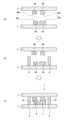
<製造方法>
図5は、本実施形態のシート状センサの製造方法の例を説明する。
すなわち、シート状の第1の基材2に抵抗体4A、5Aをパターン印刷してシート状の第1の抵抗体4A、5Aを複数形成すると共に、シート状の第2の基材3に抵抗体4B、5Bをパターン印刷して、第1の抵抗体4A、5Aと対向可能な位置にそれぞれシート状の第2の抵抗体4B、5Bを形成する。次に、第1の基材2又は第2の基材3のうちの一方の基材に対し、平面視において、1又は2以上の上記第1の抵抗体4A、5A、又は1又は2以上の第2の抵抗体4B、5Bを形成する領域の外周を囲むようにして複数の接合部6を形成する。各第1の抵抗体4A、5Aと第2の抵抗体4B、5Bとが対向するようにして第1の基材2に第2の基材3を重ねると共に、接合部6を第1の基材2又は第2の基材3のうちの他方の基材3に固着して、第1の基材2と第2の基材3を連結する。<Production Method>
FIG. 5 illustrates an example of a method for manufacturing the sheet-like sensor of this embodiment.
That is, the
シート状センサの製造方法の例を、図5を参照して具体的に説明する。
図5では、1組の荷重センサの場合を例示しているが、2組以上の荷重センサを有していてもよい。
図5(a)に示すように、第1工程において、各基材2、3上に抵抗体4A、4B、5A、5Bをパターン印刷して、シート状の第1の抵抗体4A、5Aと、シート状の第2の抵抗体4B、5Bをそれぞれ基材2、3上に形成する。
次に、図5(b)に示すように、第2工程において、接合部6を一方の基材2上に形成する。接合部6を形成する基材2、3は、どちらでも構わない。 An example of a method for manufacturing a sheet-type sensor will be specifically described with reference to FIG.
Although FIG. 5 illustrates an example in which one set of load sensors is provided, two or more sets of load sensors may be provided.
As shown in FIG. 5( a ), in the first step,
5B, in a second step, a
次に、図5(c)のように、第三工程において、対向する一対の抵抗体4A、5Aの対応する抵抗体4B、5Bの抵抗面を対向して当接させ、接合部6を挟んで一対の基材2、3を仮止めした後、接合部6を他方の基材3に接合処理することで、一対の基材2、3を接合部6で連結して固定する。
これによって、シート状センサを作製することができる。
ここで、接合部6に関して、上記のように接合材料樹脂インクを用いてパターン印刷により形成しても良いし、接合材料樹脂塗料を基材2、3と抵抗体4A、4B、5A、5Bパターンの間にコーティングして基材2、3と接合材料として熱可塑樹脂の2層のシーラント構造として、パターン加熱により接合部6の部分をラミネート接合で固定しても良い。 Next, as shown in FIG. 5( c ), in the third step, the resistive surfaces of the
In this way, a sheet-shaped sensor can be produced.
Here, the joint 6 may be formed by pattern printing using a bonding material resin ink as described above, or a bonding material resin paint may be coated between the
2.第2実施形態
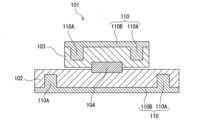
以下、図10から図16を参照して、本開示の第2実施形態にかかるシート状センサ101について説明する。
第2実施形態にかかるシート状センサ101は、媒体に加わるせん断荷重を抵抗値などの物理量変化として出力する感圧センサである。
従来のせん断荷重を計測可能なシート状の触覚センサでは、せん断荷重を表面から印加すると、センサ表面ですべりが発生してシート内の感圧層にせん断が伝わらず、正確なせん断荷重計測が困難であった。そこで、荷重印加体とセンサ表面との間に高摩擦シートを挟みすべりを軽減する方法や、荷重印加体とセンサ表面とを接着剤で固定する方法がとられてきた。高摩擦シートを挿入する方法では、高摩擦シート自体の変形や接触面のすべりが低減するものの、すべりの低減は十分ではなく、印加せん断荷重の一部しか感圧層へ伝わらなかった。また、接着剤で固定する方法では、感圧層にせん断荷重の印加は伝わるが、荷重印加体が接着剤でセンサに固定されているため破壊測定になり触覚センサとしての利用が著しく制約される問題があった。
本実施形態にかかるシート状センサ101は、シート型の触覚センサにおいても、センサ表面に印加されるせん断荷重を確実に感圧層へ伝えることができ、正確なせん断荷重測定を可能とする。2. Second Embodiment Hereinafter, a sheet-
The sheet-
In conventional sheet-type tactile sensors capable of measuring shear loads, when a shear load is applied from the surface, slippage occurs on the sensor surface, and the shear is not transmitted to the pressure-sensitive layer inside the sheet, making it difficult to measure the shear load accurately. To address this issue, methods have been used to reduce slippage by sandwiching a high-friction sheet between the load-applying body and the sensor surface, or to fix the load-applying body and the sensor surface with adhesive. With the method of inserting a high-friction sheet, the deformation of the high-friction sheet itself and the slippage of the contact surface are reduced, but the reduction in slippage is not sufficient, and only a part of the applied shear load is transmitted to the pressure-sensitive layer. With the method of fixing with adhesive, the shear load is transmitted to the pressure-sensitive layer, but since the load-applying body is fixed to the sensor with adhesive, the measurement is destructive, and there is a problem that the use of the sensor as a tactile sensor is significantly restricted.
The sheet-
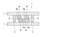
図10は、本開示のシート状センサ101の一構成例を示す断面図である。シート状センサ101には、第1の基材102と第2の基材103とに挟まれた形でセンサ素子104が形成されている。また、シート状センサ101には、基材102の主面以外の面を覆う外装部108と、基材103の主面以外の面を覆う外装部109とが形成されている。センサ表面にせん断荷重が印加されると、基材102と基材103との間にせん断荷重に応じたずり変位が発生し、基材102と基材103との間に存在するセンサ素子104に変位による歪が伝わり、せん断荷重を計測する。Figure 10 is a cross-sectional view showing an example of the configuration of the sheet-
<センサ素子>
センサ素子104の構成例としては、第1の基材102に形成された抵抗体104A(不図示)と第2の基材103上に形成された抵抗体104B(不図示)とが抵抗体表面104Aaと抵抗体表面104Baとで接触し、センサ素子104を構成する。なお、センサ素子104の抵抗体104Aと抵抗体104Bとの配置は、図3(a)及び図3(b)に示す第1の抵抗体4A及び第2の抵抗体4Bの配置と同様であるため詳細な配置の説明は省略する。
せん断荷重の印加により基材102と基材103との間にずり変位が生じると、基材102と基材103との接触面積が変化して抵抗値が上下する。この抵抗値の変化を印加した荷重で変換することで、せん断荷重を算出する。<Sensor element>
As an example of the configuration of the
When a shear displacement occurs between the
また、X方向とY方向のそれぞれのずり変位に応じて抵抗値が変化するセンサ素子を形成してもよい。すなわち、X軸センサ抗素子は、X軸方向にせん断荷重が発生したときに、第1の抵抗体104Aと第2の抵抗体104Bとの接触面積が変化して、ずり変位に応じて抵抗値などの物理量が変化する。Y軸抵抗素子は、同様にY軸方向のせん断荷重に対して抵抗値などの物理量が変化する。このような二つの抵抗素子の組み合わせでセンサ素子104を構成すれば、XY平面に印加されたせん断荷重の方向と大きさとを計測することも可能である。
センサ素子104は、せん断荷重に対して物理量が変化して検出できる構成であれば何れでもよい。センサ素子104としては、上述した抵抗値変化型のセンサが広く用いられるが、コンデンサ構造の静電容量変化型のセンサなどでも構わない。 Also, a sensor element may be formed whose resistance value changes according to shear displacement in each of the X and Y directions. That is, when a shear load is generated in the X-axis direction, the contact area between the first resistor 104A and the second resistor 104B changes in the X-axis sensor element, and a physical quantity such as a resistance value changes according to the shear displacement. Similarly, a physical quantity such as a resistance value changes in response to a shear load in the Y-axis direction in the Y-axis direction. If the
The
センサ素子104は、基材102及び基材103に、印刷またはコーティングの手法などを用いて形成する。特に印刷では、複数のセンサ素子104のそれぞれを個別に配列しやすいため好ましい。具体的には、印刷ではスクリーン印刷、グラビア印刷、インクジェットなどの手法が挙げられ、また、コーティング手法としては、グラビアコート、静電スプレー、ダイコートなどが挙げられる。コーティング手法では抵抗素子のパターンのマスクを用いて形成する。The
<基材>
基材102及び基材103は、シート状に形成可能であればどのような材料を用いてもよい。基材102及び基材103を形成する材料としては、樹脂材料を用いることが好ましく、ポリエチレン、ポリプロピレン、ポリエチレンテレフタレート、ポリカーボネート、アクリルなどを用いることができる。<Substrate>
Any material that can be formed into a sheet shape may be used for the
基材102及び103の厚さは、25μm以上300μm以下とすることが好ましい。基材102及び103の厚さがこの範囲であれば、基材102及び103が折れ曲がらず、且つ丸めたりすることができ、荷重印加体の表面が曲面であってもシート状センサ101を荷重印加体に貼着することができる。The thickness of the
<外装部>
外装部108及び外装部109は、シート状センサ101の保護とシート状センサ101への意匠性を持たせる機能を有している。
外装部108及び109は、パウチフィルムなどを基材102及び103にラミネートして形成しても良いし、保護層材料などで基材102及び103の主面を除く面の表面をコーティングして形成しても良い。さらに、外装部108及び109の表面に印刷などを施してもよい。
本実施形態では、外装部108及び109の材料及び構成は上述した材料及び構成に限定されず、使用用途により適宜選択することができる。<Exterior>
The
The
In this embodiment, the materials and configurations of the
<孔>
本実施形態にかかるシート状センサ101は、基材102及び基材103にそれぞれ二つ以上設けられた孔を備えている。孔は、外装部108の表面から基材102に通じるように設けられており、外装部108の表面から基材102の主面(基材103と対向する面)まで貫通していてもよい。孔は、外装部109及び基材103においても同様に設けられる。すなわち、孔は、外装部108及び109から基材102及び103の途中まで形成されていてもよく、基材102及び103を貫通していてもよい。<Hole>
The sheet-
図10は、外装部108及び109から基材102及び103の途中まで形成された孔105を有する第1の例のシート状センサ101(101A)を示す断面図である。また、図11は、外装部108から基材102まで貫通している孔106及び外装部109から基材103まで貫通している孔107を有する第2の例のシート状センサ101(101B)を示す断面図である。Figure 10 is a cross-sectional view showing a first example of a sheet-like sensor 101 (101A) having a
図10に示すシート状センサ101Aでは、一方の基材(例えば基材102)に設けられた孔105は、他方の基材(例えば基材103)に設けられた孔105と平面視で重ならない位置(図10及び図11の断面図においては上下方向に一致しない位置)に設けられている。同様に、図11に示すシート状センサ101Bでは、一方の基材(例えば基材102)に設けられた孔106の一部は、他方の基材(例えば基材103)に設けられた孔107と平面視で重ならない位置に設けられている。
これにより、せん断荷重が印加される際にセンサ素子104の感圧層にせん断荷重が伝わりやすくして、シート状センサ101のせん断荷重測定の正確性を向上させることができる。 In the sheet-
This makes it possible to easily transmit the shear load to the pressure-sensitive layer of the
より詳細には、せん断荷重が印加される際に垂直荷重も同時に印加されるが、基材102の孔105と基材103の孔105とが平面視において重なる位置に配置されていると、孔のエッジ部分に垂直荷重による局圧がかかってしまい、センサ素子104の感圧層にせん断荷重が伝わりにくくなる。
シート状のせん断荷重センサでは、基材102及び基材103の主面(XY面)に平行なせん断荷重を印加しようとすると、多少なりとも基材102及び基材103の厚さ方向(Z軸方向)の荷重も同時に印加される。垂直荷重の印加により基材102及び基材103が密着し、界面に摩擦が発生する。この界面摩擦と、シート状センサ101表面及び荷重印加体の間の摩擦との力関係で、センサ素子104へ伝わるせん断荷重が決まるが、多くの場合、基材102と基材103との界面摩擦が大きく、センサ素子104へのせん断荷重が伝わり難くなっている。
シート状センサ101では、基材102及び基材103の厚さ方向に延びる孔の構造体を有することで、孔を利用して印加されたせん断荷重を効率よく基材102及び103から基材102及び103と接触しているセンサ素子104に効果的に伝達することが可能となる。 More specifically, when a shear load is applied, a vertical load is also applied at the same time. However, if
In the sheet-like shear load sensor, when a shear load parallel to the main surfaces (XY planes) of the
The sheet-
図10のように基材102,103の内部で底のある孔105の形成は、レーザー加工、基材102,103表面に、または基材102,103表面上に専用層を設けたうえで型押しで形成するエンボス加工等の方法、ドリルによる物理的に形成する方法、印刷やコーティングなどで孔形成部以外を樹脂材料などでかさ上げする方法を用いることができる。
図11のように基材102,103を貫通する孔106,107の形成は、パンチや抜き刃を用いた打ち抜き形成を用いることができ、外装部108,109とともに打ち抜き加工をしても良い。 As shown in FIG. 10 , the formation of a
As shown in FIG. 11,
図12は、図10に示すシート状センサ101Aの基材102または基材103における孔105配置を示す平面模式図である。シート状センサ101では、孔は1つの基材に複数設けられていることが好ましい。孔が1つの基材に複数設けられている場合、基材102または103がXY平面の方向に対して孔を中心に回転し、感圧層に印加したせん断の方向が変化することを抑制することができる。Figure 12 is a schematic plan view showing the arrangement of
あらゆる方向からのせん断を均等に感圧層に伝えるため、図2(a)、図2(b)及び図2(c)に示すように、孔105が偶数個形成されている場合、孔105はセンサ素子104の中心Oから等距離の位置に配置される。また、図2(d)に示すように、孔105が奇数個形成されている場合、孔105はセンサ素子104の中心Oを重心とする正多角形の頂点の位置に配置される。ここで、「正多角形」は、孔の数に応じた頂点の数を有する正多角形である。
図11に示すシート状センサ101Bにおいても同様の位置に孔が配置される。 In order to transmit shear from all directions evenly to the pressure-sensitive layer, when an even number of
In the sheet-
また、シート状センサ101は、孔105内の外装部108から基材102まで貫通する治具120を備えていてもよい。すなわち、治具120は、孔105内に挿入され、孔105内で外装部108と基材102とを接続している。
図13及び図14は、孔105と治具120とを組み合わせた際のシート状センサ101の構成例を示す断面図である。基材102と基材103とにはそれぞれ二箇所以上の孔105又は孔106,107が設けられている。 The sheet-
13 and 14 are cross-sectional views showing an example of the configuration of the sheet-
図13(a)及び図13(b)は、基材102,103の内部に底を有する孔105が形成されたシート状センサ101Aにおける治具120の構成を示す断面模式図である。図13(a)に示すように、治具120は、例えば複数(例えば2つ)の孔105に挿入される突起部120Aと、突起部120A同士を外装部108、109の表面において接続する接続部120Bとを備えるピン形状であってもよい。図3(b)に示すように、このような治具120の突起部120Aは、それぞれの孔105に差し込まれている。
治具120が差し込まれた状態で外装部108を水平方向に移動させることで、治具120から孔105にせん断が伝わりセンサ素子104にせん断が伝わってせん断荷重が測定される。このようにすることで、荷重印加体とシート状センサ101との間の摩擦力に頼ることなく正確なせん断荷重の測定が可能となる。また、シート状センサ101の使用後に治具120を取り出すことにより、シート状センサ101は再利用可能となる。 13(a) and 13(b) are schematic cross-sectional views showing the configuration of a
By moving the
治具120は、孔105の径より小さい径の円筒ピンを突起部120Aとして有する構造体とすることができる。治具120を構成する材料としては、金属やセラミックなどせん断が与えられたとき変形しない材料を選択することができる。The
図14は、基材102,103を貫通する孔106及び107が形成されたシート状センサ101Bにおける治具120の構成を示す断面模式図である。シート状センサ101Bでは、貫通した先に同じ外形を持つ孔が配置されないようにするため、基材102,103のうちの一方の外形を他方よりも小さくして、他方に形成された孔106だけを治具120の突起部120Aが貫通するようにする。Figure 14 is a schematic cross-sectional view showing the configuration of the
図14では、基材103の外形を基材102より小さくして、基材102の基材103と重ならない部分に貫通する孔106を形成している。基材102と基材103とが重なった部分に孔106及び孔107を形成する場合は、基材103に形成された孔107の下側に基材102の孔106を形成する。このとき、基材102側の孔106の外径を孔107の外径よりも大きく形成している。一方の孔(孔106)の外径を大きくする量は、せん断印加でずり変位が起きる量に設定することが好ましい。せん断測定時に基材103側から挿入した治具120が基材102に形成された孔106に当たることがなくなるためである。せん断荷重印加によるずり変位量は数百μm程度であるため、対向する孔106の外径と孔107の外径との差は1mm程度とすることが好ましい。具体的には、孔107が2mm径の場合は、孔107に対向する孔106の孔径を3mmにすればよい。In FIG. 14, the outer shape of the
図15は、治具120と図10に示すシート状センサ101Aを一体化した場合のシート状センサ101の構成例を示す断面図である。載荷重層110は、孔105を埋める突起部110Aと、基材102及び基材103の表面にそれぞれ形成される接続部110Bとを有している。
載荷重層110を形成する材料としては、金属やセラミックなど剛体が選定される。載荷重層110を形成する材料として樹脂などの粘性成分を持つ材料を用いることも可能であるが、この場合にはせん断が突起部110Aに伝わり難くなるため、硬質樹脂を選択するか、硬化処理をした材料を選択する。基材102,103の表面において載荷重層110を形成する部分は、実際に荷重印加する場所に限定するとよい。このような一体化構成をとることで、治具120を別に準備することなくせん断荷重をセンサ素子104に伝えることが可能となる。
図11に示すシート状センサ101Bにおいても同様の一体化構造をとることができる。 Fig. 15 is a cross-sectional view showing a configuration example of the sheet-
A rigid body such as metal or ceramic is selected as the material for forming the
A similar integrated structure can also be adopted in the sheet-
図16は、シート状センサ101に荷重印加体130によるせん断荷重が印加された状態を示す模式図である。荷重印加体130は、せん断測定をしたい対象物であり、特に形状、材質に制約はない。荷重印加体130によりせん断が斜めに印加されると、せん断荷重成分は、基材103の孔105で載荷重層110の突起部110Aによりせん断としてセンサ素子104に伝わる。載荷重層110の表面は荷重印加体130との摩擦が大きくなるように材料と表面形状を選択することができる。高摩擦になれば素材や形状には制約がないが、例えば、微小突起が形成された金属やセラミックなどが選択される。
このようにして、XY平面全方位のせん断荷重をシート形状の媒体にて安定な計測を可能とするシート状センサ101が得られる。 FIG. 16 is a schematic diagram showing a state in which a shear load is applied to the sheet-
In this manner, a sheet-
<変形例>
センサ素子104は、せん断を物理量変化として感知する感圧層とともに、せん断荷重に対して弾性的に動作し、基材102と基材103とを接合する弾性接合部(図10中不図示)を有していてもよい。弾性接合部が設けられることにより、せん断荷重が開放されたときに、基材102又は基材103が初期の位置に復元することが可能になり、連続変化するせん断荷重が印加された場合におけるせん断荷重の計測が容易になる。<Modification>
The
また、シート状センサ101は、抵抗値変化型の垂直荷重用センサをさらに備えることで、X軸方向とY軸方向とに加えてZ軸方向を検出方向とする3軸センサとすることもできる。また、センサ素子104は、物理量変化出力の引き出し配線を有していてもよい。引き出し配線としては、プリント配線板を用いても良いし、銀ペーストなどの導電インクを用いて印刷してもよい。The sheet-
3.使用例
以下、シート状センサの使用例について説明する。以下では、第1実施形態のシート状センサ1の使用例を一例として説明する。
本実施形態のシート状センサは、ケースの中に挿入するインレイとすることもできる。このインレイをケースの中に挿入することで2次元センサとできる。インレイを入れるケースは、インレイ毎のポケットがあってもよい。そして、ポケットの中にインレイを挿入してもよい。これにより、インレイを所定の位置に配置できる。また、各シート状センサは、かみ合わせなどで、ケースの中で固定されていてもよい。この固定は、2次元センサに圧力が掛かったときに固定されてもよい。また、インレイの固定は、着脱可能でもよい。着脱可能とすることで、インレイが破損した場合の交換が容易となる。2次元センサは、カバーの中に収容されて使用してもよい。ケースが袋体であり、ケースの内部にシート状センサを敷き詰めても良い。3. Examples of Use The following describes examples of use of the sheet-
The sheet-like sensor of this embodiment may be an inlay inserted into a case. By inserting this inlay into the case, a two-dimensional sensor can be formed. The case for inserting the inlay may have a pocket for each inlay. The inlay may be inserted into the pocket. This allows the inlay to be positioned at a predetermined position. Each sheet-like sensor may be fixed in the case by interlocking or the like. This fixation may occur when pressure is applied to the two-dimensional sensor. The fixation of the inlay may be detachable. By making the inlay detachable, it becomes easy to replace the inlay if it is damaged. The two-dimensional sensor may be housed in a cover and used. The case may be a bag body, and the sheet-like sensors may be laid out inside the case.
図17は、帯状の基材2、3間に1組の荷重センサが設けられたシート状センサからなるインレイ70を示す。
図18では、図17に示すインレイ70をケースにマトリックス状に配列した2次元センサ71が説明されている。このインレイ70の配置は、等間隔、又は領域毎に異なった間隔とすることができる。領域毎に異なった間隔とすることで、センシングの密度を面内で変えることができる。等間隔に配置すれば均一にセンシングができる。インレイ70を構成する各シート状センサは、2組以上の荷重センサを有していてもよい。 FIG. 17 shows an
Fig. 18 illustrates a two-
ケースの端部、又はポケットの端部は、シールされていてもよい。シールは防水性のでもよい。このシールはジッパーでもよい。防水性のシールは、インレイへの浸水による故障を防止できる。また防水性のシールは、特にケースをベッドに敷いた場合に、インレイの汚染を防止できる。防水性のシールを端部に有するケースにインレイを挿入した2次元センサ71は、衛生面で優れている。The ends of the case or the ends of the pocket may be sealed. The seal may be waterproof. The seal may be a zipper. A waterproof seal can prevent damage to the inlay due to water ingress. A waterproof seal can also prevent contamination of the inlay, especially when the case is placed on a bed. A two-
なお、1組の荷重センサを構成する複数のセンサ素子の1つが圧力センサ素子の場合は、静電容量方式のものとしてもよい。また圧力センサ素子が圧電素子から構成されていてもよい。上記のような温度センサ素子を併設してもよい。温度センサ素子は、圧力センサ素子の校正用として用いることもできる。特にインレイ70を用いた場合には、そのインレイ70の個数を増やすことで容易に大面積化することができる。When one of the multiple sensor elements constituting a load sensor set is a pressure sensor element, it may be of the capacitance type. The pressure sensor element may also be composed of a piezoelectric element. A temperature sensor element as described above may also be provided. The temperature sensor element may also be used to calibrate the pressure sensor element. In particular, when an
<作用効果>
本開示の態様によれば、せん断荷重等を第1の抵抗体4A、5Aと第2の抵抗体4B、5Bの表面接触面積の抵抗値変化で検出するセンサ素子4、5の構成部品をシート状に構成することで、印刷法にてシート状センサが製造可能となる。この結果、本開示の態様によれば、複数のセンサ素子4、5を配置して大面積のシート状センサを構成しても、印刷での製造が可能な安価なセンサであって、寸法的に大面積化が可能なシート状センサを提供可能となる。
このようにして、本開示により、XY平面全方位のせん断荷重をシート形状の媒体にて安定に計測を可能とする荷重センサを提供可能とした。<Action and effect>
According to the aspect of the present disclosure, a sheet-like sensor can be manufactured by a printing method by configuring the components of the
In this way, the present disclosure makes it possible to provide a load sensor that can stably measure shear loads in all directions on the XY plane using a sheet-shaped medium.
<その他>
本開示は、以下のような構成も取ることができる。
(1)対向する一対のシート状の基材の間に、2以上のセンサ素子が配置され、前記各センサ素子は、前記一対の基材のうちの一方の基材に形成されたシート状の第1の抵抗体と、他方の基材に形成されたシート状の第2の抵抗体とが対向配置すると共に、前記第1の抵抗体と前記第2の抵抗体とは、前記第1の抵抗体に対し前記第2の抵抗体が相対変位可能な状態で接触し、更に、前記一対の基材間を連結して、各センサ素子における、前記第1の抵抗体に対する前記第2の抵抗体の位置決めを行う接合部を有する、シート状センサ。<Other>
The present disclosure can also be configured as follows.
(1) A sheet-type sensor comprising: two or more sensor elements disposed between a pair of opposing sheet-type substrates; each of the sensor elements is disposed such that a sheet-type first resistor formed on one of the pair of substrates faces a sheet-type second resistor formed on the other of the pair of substrates; the first resistor and the second resistor are in contact with each other in a state in which the second resistor can be displaced relatively to the first resistor; and a joint that connects the pair of substrates and positions the second resistor relative to the first resistor in each sensor element.
(2)前記2以上のセンサ素子は、複数のセンサ素子毎にセンサの組を構成する。
(3)前記接合部は、前記センサの組毎に3個以上設けられ、前記3個以上の接合部は、平面視において、対応するセンサの組を構成する2以上のセンサ素子の質量中心を中心とした第1の円の円状にそれぞれ配置されると共に、隣り合う接合部間の距離が等間隔になっている。(2) The two or more sensor elements form a sensor set for each of the plurality of sensor elements.
(3) Three or more of the joints are provided for each pair of sensors, and the three or more joints are arranged, in a planar view, in a circular shape of a first circle centered on the center of mass of two or more sensor elements that constitute the corresponding pair of sensors, and the distance between adjacent joints is equal.
(4)センサの組を構成する2以上のセンサ素子は、前記質量中心を中心した第2の円に内接するように配置され、前記第1の円の半径は、前記第2の円の半径の2倍以下である。
(5)前記センサの組を構成する複数のセンサ素子に、せん断力を検知するせん断力検知センサを2以上含み、平面視において、前記2以上のせん断力検知センサが検知するせん断力の方向が互いに異なり、各せん断力検知センサの対向配置された2つの抵抗体は、平面視において、検知するせん断力の方向へのせん断変位に応じて、前記2つの抵抗体の重なる領域の面積が変化すると共に、前記検知するせん断力の方向と直交する方向のせん断変位に対し、前記2つの抵抗体の重なる領域の面積が一定に維持されるように、前記2つの抵抗体の形状及び配置が構成されている。
(6)前記センサの組を複数、有し、平面視において、前記複数のセンサの組が、マトリックス状に配置されている。(4) Two or more sensor elements constituting a sensor group are arranged so as to be inscribed in a second circle centered on the center of mass, and the radius of the first circle is less than or equal to twice the radius of the second circle.
(5) The multiple sensor elements constituting the sensor group include two or more shear force detection sensors that detect shear force, and in a planar view, the directions of the shear forces detected by the two or more shear force detection sensors are different from each other. The two resistors arranged opposite each other in each shear force detection sensor are configured in shape and arrangement such that, in a planar view, the area of the overlapping area of the two resistors changes in response to shear displacement in the direction of the shear force to be detected, while the area of the overlapping area of the two resistors is maintained constant against shear displacement in a direction perpendicular to the direction of the shear force to be detected.
(6) The sensor device includes a plurality of sets of sensors, and the plurality of sets of sensors are arranged in a matrix in plan view.
(7)主面を除く面が外装部で覆われている一対の基材と、前記一対の基材の主面同士の間に配置されたセンサ素子と、前記一対の基材それぞれの前記外装部の表面から前記基材に通じるように設けられた孔と、を備え、前記一対の基材のうちの一方の基材に設けられた孔は、前記一対の基材のうちの他方の基材に設けられた孔と平面視で重ならない位置に設けられている、シート状センサ。
(8)前記孔は、前記一対の基材のそれぞれに複数設けられており、前記孔が偶数個設けられている場合は、平面視で前記センサ素子の中心から等距離の位置に配置され、前記孔が奇数個設けられている場合は、平面視で前記センサ素子の中心を重心とする正多角形の頂点の位置に設けられている。(7) A sheet-type sensor comprising a pair of substrates whose surfaces except for the main surfaces are covered with exterior parts, a sensor element arranged between the main surfaces of the pair of substrates, and holes provided from the surfaces of the exterior parts of each of the pair of substrates to the substrate, wherein the holes provided in one of the pair of substrates are provided at a position that does not overlap with holes provided in the other of the pair of substrates in a planar view.
(8) The holes are provided in multiple numbers in each of the pair of substrates, and when an even number of holes are provided, the holes are arranged at positions equidistant from the center of the sensor element in a planar view. When an odd number of holes are provided, the holes are arranged at the vertices of a regular polygon having the center of gravity at the center of the sensor element in a planar view.
(9)前記孔内の前記外装部から前記基材まで貫通する治具を備えている。
(10)前記治具は、ピン形状である。(9) A jig is provided that penetrates from the exterior portion within the hole to the base material.
(10) The jig is pin-shaped.
(11)前記治具が、金属又はセラミックで形成されている。
(12)前記孔は、前記外装部の表面から前記基材の前記主面まで貫通し、前記一対の基材のうちの一方の基材の主面に設けられた孔は、前記一対の基材のうちの他方の基材に設けられた孔と平面視で重なる位置に設けられており、前記治具同士が、前記基材の主面で接続されている。(11) The jig is made of metal or ceramic.
(12) The holes penetrate from the surface of the exterior portion to the main surface of the substrate, a hole provided on the main surface of one of the pair of substrates is provided at a position overlapping in a planar view with a hole provided on the other of the pair of substrates, and the jigs are connected to each other via the main surfaces of the substrates.
(13)シート状の第1の基材に抵抗体をパターン印刷して第1の抵抗体を複数形成し、シート状の第2の基材に抵抗体をパターン印刷して、前記第1の抵抗体と対向可能な位置に第2の抵抗体を形成し、前記第1の基材又は第2の基材のうちの一方の基材に対し、平面視において、1又は2以上の前記第1の抵抗体又は1又は2以上の前記第2の抵抗体を形成する領域の外周を囲むようにして、複数の接合部を形成し、前記各第1の抵抗体と第2の抵抗体とが対向するようにして前記第1の基材に第2の基材を重ねると共に、前記接合部を前記第1の基材又は第2の基材のうちの他方の基材に固着して、前記第1の基材と前記第2の基材を連結する。(13) A resistor is pattern-printed on a sheet-like first substrate to form a plurality of first resistors, a resistor is pattern-printed on a sheet-like second substrate to form a second resistor at a position that can face the first resistor, and a plurality of joints are formed on one of the first substrate or the second substrate so as to surround the periphery of an area in which one or more of the first resistors or one or more of the second resistors are formed in a plan view, and the second substrate is overlaid on the first substrate so that each of the first resistors faces the second resistor, and the joints are fixed to the other of the first substrate or the second substrate to connect the first substrate and the second substrate.
次に、第1実施形態に基づく実施例について説明する。Next, we will explain an example based on the first embodiment.
(1)実施例1
<実施例1-1>
以下の方法により、図1に示す構造のシート状センサを形成した。
基材として100μmのPETフィルムを用いた。一対の基材の上に、それぞれカーボンインク(十条ケミカル製、商品名:JELCON CH-N)を用いて抵抗体をそれぞれ印刷した。このとき、一方の基材の一方の面上にシート状の第1の抵抗体とシート状の第2の抵抗体とを形成するとともに、他方の基材の一方の面上にシート状の第1の抵抗体とシート状の第2の抵抗体とを形成し、抵抗体同士を接触させてセンサ素子を形成した。各抵抗体は、2つのセンサ素子の質量中心を中心とする半径7mmに内接するようにして形成する。
センサ素子の外周に設ける接合部の材料として、ポリエチレン(日本ポリエチレン製、商品名:ノバテックLC525)を使用した。そして、3つの接合部は、2つのセンサ素子の質量中心を中心とした10mm位置範囲であって、上記中心に対する正三角形の頂点の位置にそれぞれ形成した。各接合部は、直径φ3mmの円柱体とした。(1) Example 1
<Example 1-1>
A sheet-like sensor having the structure shown in FIG. 1 was formed by the following method.
A 100 μm PET film was used as the substrate. Resistors were printed on each of the pair of substrates using carbon ink (manufactured by Jujo Chemical, product name: JELCON CH-N). At this time, a sheet-shaped first resistor and a sheet-shaped second resistor were formed on one surface of one substrate, and a sheet-shaped first resistor and a sheet-shaped second resistor were formed on one surface of the other substrate, and the resistors were brought into contact with each other to form a sensor element. Each resistor was formed so as to be inscribed within a radius of 7 mm centered on the center of mass of the two sensor elements.
Polyethylene (made by Nippon Polyethylene, product name: Novatec LC525) was used as the material for the joints on the outer periphery of the sensor element. The three joints were formed within a 10 mm range from the center of mass of the two sensor elements, at the vertices of an equilateral triangle with respect to the center. Each joint was a cylinder with a diameter of φ3 mm.
そして、接合部が形成された一方の基材と他方の基材とを、それぞれの対向する抵抗体の対向面を合わせると共に、接合部を挟んで仮止めし、120度でホットラミネートして接合部の先端部を基材に固着させた。
以上によって、1組の荷重センサを有するシート状センサを作製した。
そのシート状センサに対し、Z軸の垂直荷重20Nを加え、水平方向に8Nのせん断荷重を印加したところ、XY方向にそれぞれに対応するセンサ素子4、5の抵抗値が200Ω±30Ωの範囲で変化することが観察された。 Then, one of the substrates on which the joint was formed was aligned with the other substrate so that the opposing surfaces of the resistors facing each other were aligned, the substrate was temporarily secured in place with the joint sandwiched between them, and the substrate was hot laminated at 120 degrees to fix the tip of the joint to the substrate.
In this manner, a sheet-type sensor having a set of load sensors was fabricated.
When a vertical load of 20 N was applied to the sheet-like sensor in the Z-axis direction and a shear load of 8 N was applied in the horizontal direction, it was observed that the resistance values of the
(2)実施例2
以下、第2実施形態に基づく実施例について説明する。(2) Example 2
Examples based on the second embodiment will be described below.
<実施例2-1>
以下の方法により、図10に示す構造のシート状センサを形成した。
基材として100μmのPETフィルムを用いた。一対の基材の上に、それぞれカーボンインク(十条ケミカル製、商品名:JELCON CH-N)を用いて抵抗体をそれぞれ印刷した。このとき、せん断力検出方向において一対の抵抗体の一部同士が重複するように抵抗体同士を接触させてセンサ素子を形成した。一方向にせん断によるずり変位が起きると、抵抗体同士の接触面積が変わりせん断荷重変化を抵抗変化として測定できる。打ち抜き刃を用いて一対の基材のそれぞれに2.0mm径の貫通孔を形成した。接合部材料として、両面テープ(寺岡製作所、7070W)を用いて一対の基材を固定して実施例2-1のシート状センサを作製した。
一対の基材のそれぞれに設けた貫通孔の位置に合わせて1.9mm径のピン形状の治具を作製した。治具を一対の基材のそれぞれに設けた貫通孔に差し込み、一方の治具を固定し、もう一方の治具にずり変位を印加する手法でせん断荷重を印加した。<Example 2-1>
A sheet-like sensor having the structure shown in FIG. 10 was formed by the following method.
A 100 μm PET film was used as the substrate. Resistors were printed on the pair of substrates using carbon ink (manufactured by Jujo Chemical, product name: JELCON CH-N). At this time, the pair of resistors were contacted with each other so that parts of them overlap in the shear force detection direction to form a sensor element. When shear displacement occurs in one direction due to shear, the contact area between the resistors changes, and the shear load change can be measured as a resistance change. A punch blade was used to form a through hole with a diameter of 2.0 mm in each of the pair of substrates. A pair of substrates was fixed using double-sided tape (Teraoka Seisakusho, 7070W) as a joint material to prepare a sheet-like sensor of Example 2-1.
A pin-shaped jig with a diameter of 1.9 mm was prepared to match the positions of the through holes provided in each of the pair of substrates. The jig was inserted into the through holes provided in each of the pair of substrates, and a shear load was applied by fixing one of the jigs and applying a shear displacement to the other jig.
<比較例2-1>
実施例2―1のセンサに孔を設けないこと以外は、実施例2-1と同様にして比較例2-2を作製した。<Comparative Example 2-1>
Comparative Example 2-2 was prepared in the same manner as in Example 2-1, except that no holes were provided in the sensor of Example 2-1.
せん断時には、高摩擦シート(イノアック社;ポロンMX-48HF)を押し当てせん断印加をした。
実施例2-1と比較例2-1に対して、垂直荷重を10N又は20Nに保持してシート状センサにせん断を加えた。
以下の表1に、上述の垂直荷重を保持した際のせん断荷重[N]を示す。 During shearing, a high friction sheet (INOAC Corporation; Poron MX-48HF) was pressed against the sample to apply shear.
For Example 2-1 and Comparative Example 2-1, a vertical load was maintained at 10 N or 20 N to apply shear to the sheet-like sensor.
Table 1 below shows the shear load [N] when the above-mentioned vertical load was maintained.

表1に示す通り、実施例2-1では、せん断荷重を垂直荷重と同じ10N又は20Nまで印加できた。一方、比較例2-1では、それぞれ3Nまでしか印加できず、この時点で、高摩擦シートとセンサの接触面でずれが生じることが確認できた。As shown in Table 1, in Example 2-1, a shear load of up to 10 N or 20 N, the same as the normal load, could be applied. On the other hand, in Comparative Example 2-1, only a load of 3 N could be applied, and at this point, it was confirmed that a shift occurred at the contact surface between the high friction sheet and the sensor.
以上、本開示を実施の形態を用いて説明したが、本開示の技術的範囲は上記実施の形態に記載の範囲には限定されない。上記実施の形態に、多様な変更又は改良を加えることが可能であることが当業者に明らかである。その様な変更又は改良を加えた形態も本開示の技術的範囲に含まれ得ることが、特許請求の範囲の記載から明らかである。Although the present disclosure has been described above using embodiments, the technical scope of the present disclosure is not limited to the scope described in the above embodiments. It is clear to those skilled in the art that various modifications and improvements can be made to the above embodiments. It is clear from the claims that forms incorporating such modifications or improvements can also be included in the technical scope of the present disclosure.
1,101,101A,101B シート状センサ
2,3,102,103 基材
4,5,104 センサ素子
4A,5A,104A 第1の抵抗体
4Aa,5Aa,104Aa 抵抗体表面
4B,5B,104B 第2の抵抗体
4Ba,5Ba,104Ba 抵抗体表面
6 接合部
7 第1の抵抗体
8 第2の抵抗体
10 接触面
20 第2の円
30 第1の円
40 温度センサ素子
41 接触面
70 インレイ
71 2次元センサ
105,106,107 孔
108,109 外装部
110 載荷重層
110A 突起部
110B 接続部
120 治具
120A 突起部
120B 接続部
130 荷重印加体1, 101, 101A, 101B Sheet-
Claims (9)
Translated fromJapanese前記各センサ素子は、前記一対の基材のうちの一方の基材に形成されたシート状の第1の抵抗体と、他方の基材に形成されたシート状の第2の抵抗体とが対向配置すると共に、前記第1の抵抗体と前記第2の抵抗体とは、前記第1の抵抗体に対し前記第2の抵抗体が相対変位可能な状態で接触し、
更に、前記一対の基材間を連結して、各センサ素子における、前記第1の抵抗体に対する前記第2の抵抗体の位置決めを行う接合部を有しており、
2以上の前記センサ素子は、複数のセンサ素子毎にセンサの組を構成しており、
前記センサの組を構成する複数の前記センサ素子に、せん断力を検知するせん断力検知センサを2以上含み、
平面視において、前記2以上のせん断力検知センサが検知するせん断力の方向が互いに異なり、
各せん断力検知センサの対向配置された2つの抵抗体は、平面視において、検知するせん断力の方向へのせん断変位に応じて、前記2つの抵抗体の重なる領域の面積が変化すると共に、前記検知するせん断力の方向と直交する方向のせん断変位に対し、前記2つの抵抗体の重なる領域の面積が一定に維持されるように、前記2つの抵抗体の形状及び配置が構成されている
シート状センサ。 Two or more sensor elements are disposed between a pair of opposing sheet-like substrates;
Each of the sensor elements has a sheet-like first resistor formed on one of the pair of base materials and a sheet-like second resistor formed on the other base material, the first resistor and the second resistor being in contact with each other in a state in which the second resistor is displaceable relative to the first resistor;
The sensor element furtherincludes a joint portion that connects the pair of base materials and positions the second resistor relative to the first resistor in each sensor element,
The two or more sensor elements constitute a sensor set for each of the plurality of sensor elements,
The plurality of sensor elements constituting the sensor group include two or more shear force detection sensors that detect shear force,
In a plan view, directions of shear forces detected by the two or more shear force detection sensors are different from each other,
A sheet-type sensor in which two resistors arranged opposite each other in each shear force detection sensor are shaped and arranged so that, when viewed in a plane, the area of the overlapping region of the two resistors changes in response to shear displacement in the direction of the shear force to be detected, while the area of the overlapping region of the two resistors is maintained constant for shear displacement in a direction perpendicular to the direction of the shear force to be detected .
3個以上の前記接合部は、平面視において、対応するセンサの組を構成する2以上の前記センサ素子の質量中心を中心とした第1の円の円状にそれぞれ配置されると共に、隣り合う接合部間の距離が等間隔になっている、
請求項1に記載したシート状センサ。 Three or more of the joints are provided for each set of the sensors,
The three or more joints are respectively arranged in a circular shape of a first circle centered on the center of mass of the two or more sensor elements constituting the corresponding sensor set in a plan view, and the distance between adjacent joints is equal.
2. The sheet-like sensor according to claim1 .
前記第1の円の半径は、前記第2の円の半径の1倍以上2倍以下である、
請求項2に記載したシート状センサ。 The two or more sensor elements constituting a sensor set are arranged so as to be inscribed in a second circle centered on the center of mass,
The radius of the first circle is equal to or greater than 1 time and equal to or less than 2 times the radius of the second circle.
3. The sheet-like sensor according to claim2 .
平面視において、複数の前記センサの組が、マトリックス状に配置されている、
請求項1~請求項3のいずれか1項に記載したシート状センサ。 A plurality of sets of the sensors are provided,
In a plan view, the plurality of sensor sets are arranged in a matrix.
The sheet-like sensor according to any one of claims1 to3 .
前記一対の基材の主面同士の間に配置されたセンサ素子と、
前記一対の基材それぞれを覆う前記外装部の表面から前記基材に通じるように設けられた孔と、
を備え、
前記一対の基材のうちの一方の基材に設けられた孔は、前記一対の基材のうちの他方の基材に設けられた孔と平面視で重ならない位置に設けられており、
前記孔内の前記外装部から前記基材まで貫通する治具を備えており、
前記孔は、前記外装部の表面から前記基材の前記主面まで貫通し、前記一対の基材のうちの一方の基材の主面に設けられた孔は、前記一対の基材のうちの他方の基材に設けられた孔と平面視で重なる位置に設けられており、
前記治具の同士が、前記基材の主面で接続されている
シート状センサ。 A pair of substrates, the surfaces of which except for the main surfaces are covered with exterior parts;
A sensor element disposed between the main surfaces of the pair of base materials;
a hole provided from a surface of the exterior portion covering each of the pair of base materials to the base material;
Equipped with
a hole provided in one of the pair of substratesis provided at a position not overlapping with a hole provided in the other of the pair of substrates in a plan view;
A jig is provided that penetrates from the exterior portion to the base material within the hole,
the holes penetrate from a surface of the exterior portion to the main surface of the base material, and a hole provided in the main surface of one of the pair of base materials is provided at a position overlapping with a hole provided in the other of the pair of base materials in a plan view;
A sheet-like sensorin which the jigs are connected to each other via the main surfaces of the base material .
ている場合は、平面視で前記センサ素子の中心から等距離の位置に配置され、前記孔が奇数個設けられている場合は、平面視で前記センサ素子の中心を重心とする正多角形の頂点の位置に設けられている
請求項5に記載したシート状センサ。 The sheet-type sensor of claim 5, wherein the holes are provided in a plurality of positions in each of the pair of substrates, and when an even number of the holes are provided, the holes are arranged at positions equidistant from the center of the sensor element in a planar view, and when an odd number of the holes are provided, the holes are arranged at the vertices of a regular polygon having the center of gravity at the center of the sensor element ina planar view.
請求項5又は請求項6に記載したシート状センサ。 7. The sheet-like sensor according toclaim 5 , wherein the jig is in the shape of a pin.
請求項5から請求項7のいずれか1項に記載したシート状センサ。 8. The sheet-like sensoraccording to claim 5 , wherein the jig is made of metal or ceramic.
シート状の第2の基材に抵抗体をパターン印刷して、前記第1の抵抗体と対向可能な位置に第2の抵抗体を形成し、
前記第1の基材又は第2の基材のうちの一方の基材に対し、平面視において、1又は2以上の前記第1の抵抗体又は1又は2以上の前記第2の抵抗体を形成する領域の外周を囲むようにして、複数の接合部を形成し、
前記第1の抵抗体と前記第2の抵抗体とが対向するようにして前記第1の基材に第2の基材を重ねると共に、前記接合部を前記第1の基材又は第2の基材のうちの他方の基材に固着して、前記第1の基材と前記第2の基材を連結して、センサ素子を形成するとともに、2以上の前記センサ素子を、複数のセンサ素子毎にセンサの組とし、前記センサの組を構成する複数の前記センサ素子に、せん断力を検知するせん断力検知センサを2以上含み、平面視において、前記2以上のせん断力検知センサが検知するせん断力の方向が互いに異なり、各せん断力検知センサの対向配置された前記第1の抵抗体及び前記第2の抵抗体は、平面視において、検知するせん断力の方向へのせん断変位に応じて、前記第1の抵抗体及び前記第2の抵抗体の重なる領域の面積が変化すると共に、前記検知するせん断力の方向と直交する方向のせん断変位に対し、前記第1の抵抗体及び前記第2の抵抗体の重なる領域の面積が一定に維持されるように、前記第1の抵抗体及び前記第2の抵抗体の形状及び配置を構成する、
シート状センサの製造方法。 forming a plurality of first resistors by printing a resistor pattern on a sheet-like first base material;
a resistor pattern is printed on a sheet-like second base material to form a second resistor at a position opposite to the first resistor;
a plurality of bonding portions are formed on one of the first base material and the second base material so as to surround an outer periphery of a region in which one or more of the first resistors or one or more of the second resistors are formed in a plan view;
A second base material is overlaid on the first base material such that the first resistor and the second resistor face each other, and the joint portion is fixed to the other of the first base material and the second base materialto connect the first base material and the second base material to form a sensor element, and two or more of the sensor elements are grouped into a sensor set for each of the plurality of sensor elements, and the plurality of sensor elements constituting the sensor set include two or more shear force detection sensors that detect a shear force, and the two or more shear force detection sensors are The directions of the shear forces to be detected are different from each other, and the first resistor and the second resistor arranged opposite to each other in each shear force detection sensor are configured to have shapes and arrangements such that, in a plan view, an area of an overlapping region of the first resistor and the second resistor changes in response to shear displacement in the direction of the shear force to be detected, and the area of the overlapping region of the first resistor and the second resistor is maintained constant with respect to shear displacement in a direction perpendicular to the direction of the shear force to be detected .
A method for manufacturing a sheet-type sensor.
Priority Applications (1)
| Application Number | Priority Date | Filing Date | Title |
|---|---|---|---|
| PCT/JP2022/006994WO2022190840A1 (en) | 2021-03-10 | 2022-02-21 | Sheet-like sensor, and method for manufacturing same |
Applications Claiming Priority (2)
| Application Number | Priority Date | Filing Date | Title |
|---|---|---|---|
| JP2021038365 | 2021-03-10 | ||
| JP2021038365 | 2021-03-10 |
Publications (2)
| Publication Number | Publication Date |
|---|---|
| JP2022140219A JP2022140219A (en) | 2022-09-26 |
| JP7643212B2true JP7643212B2 (en) | 2025-03-11 |
Family
ID=83400062
Family Applications (1)
| Application Number | Title | Priority Date | Filing Date |
|---|---|---|---|
| JP2021109191AActiveJP7643212B2 (en) | 2021-03-10 | 2021-06-30 | Sheet-like sensor and its manufacturing method |
Country Status (1)
| Country | Link |
|---|---|
| JP (1) | JP7643212B2 (en) |
Citations (5)
| Publication number | Priority date | Publication date | Assignee | Title |
|---|---|---|---|---|
| JP2003509685A (en) | 1999-09-13 | 2003-03-11 | エンカース エスアールエル | Small external force distribution sensor |
| JP2015169532A (en) | 2014-03-06 | 2015-09-28 | 国立大学法人信州大学 | Sheet sensor system and sheet sensor |
| WO2018042685A1 (en) | 2016-08-30 | 2018-03-08 | 株式会社フジクラ | Load detection sensor unit |
| JP2019184573A (en) | 2018-04-05 | 2019-10-24 | 三星ディスプレイ株式會社Samsung Display Co.,Ltd. | Force sensor |
| JP2020016549A (en) | 2018-07-25 | 2020-01-30 | 凸版印刷株式会社 | Tactile sensor and manufacturing method therefor |
Family Cites Families (1)
| Publication number | Priority date | Publication date | Assignee | Title |
|---|---|---|---|---|
| US6216545B1 (en)* | 1995-11-14 | 2001-04-17 | Geoffrey L. Taylor | Piezoresistive foot pressure measurement |
- 2021
- 2021-06-30JPJP2021109191Apatent/JP7643212B2/enactiveActive
Patent Citations (5)
| Publication number | Priority date | Publication date | Assignee | Title |
|---|---|---|---|---|
| JP2003509685A (en) | 1999-09-13 | 2003-03-11 | エンカース エスアールエル | Small external force distribution sensor |
| JP2015169532A (en) | 2014-03-06 | 2015-09-28 | 国立大学法人信州大学 | Sheet sensor system and sheet sensor |
| WO2018042685A1 (en) | 2016-08-30 | 2018-03-08 | 株式会社フジクラ | Load detection sensor unit |
| JP2019184573A (en) | 2018-04-05 | 2019-10-24 | 三星ディスプレイ株式會社Samsung Display Co.,Ltd. | Force sensor |
| JP2020016549A (en) | 2018-07-25 | 2020-01-30 | 凸版印刷株式会社 | Tactile sensor and manufacturing method therefor |
Also Published As
| Publication number | Publication date |
|---|---|
| JP2022140219A (en) | 2022-09-26 |
Similar Documents
| Publication | Publication Date | Title |
|---|---|---|
| US9671297B2 (en) | Pliable pressure-sensing fabric | |
| EP1700091B1 (en) | A sensor | |
| US7942072B2 (en) | Flexible force sensor with coupling type and multi-directional recognitions | |
| TWI530672B (en) | Input device and input device control method | |
| US12066339B2 (en) | System and method of detecting force applied to an object using pressure-sensitive sheets | |
| JP2009031089A (en) | Sensor sheet | |
| JP6979806B2 (en) | Elastic force sensor | |
| JP2009192256A (en) | Pressure sensor and robot hand system | |
| US20170234673A1 (en) | Pliable pressure-sending fabric | |
| US20250314538A1 (en) | High-resistance sensor and method for using same | |
| JP7118054B2 (en) | flexible sensor | |
| JP7643212B2 (en) | Sheet-like sensor and its manufacturing method | |
| WO2022255031A1 (en) | Finger with tactile sensor for robot hand and robot hand with tactile sensor using same | |
| WO2022190840A1 (en) | Sheet-like sensor, and method for manufacturing same | |
| JP7532828B2 (en) | Tactile sensor and method for manufacturing same | |
| WO2019003946A1 (en) | Sensor sheet, capacitive sensor, and method for manufacturing sensor sheet | |
| JP2005351653A (en) | Pressure sensor | |
| JP2023542467A (en) | force sensing device | |
| JP2023165261A (en) | Sheet type load sensor | |
| CN107688405A (en) | Touch pressure sensing device further and electronic product | |
| KR20220085068A (en) | flexible multi-modal tactile sensor | |
| JP6489710B2 (en) | Capacitance type 3D sensor | |
| JP2022076611A (en) | Stress sensor, manufacturing method thereof, and sensor sheet | |
| TWM592603U (en) | Composite thin film sensor |
Legal Events
| Date | Code | Title | Description |
|---|---|---|---|
| A621 | Written request for application examination | Free format text:JAPANESE INTERMEDIATE CODE: A621 Effective date:20240522 | |
| A131 | Notification of reasons for refusal | Free format text:JAPANESE INTERMEDIATE CODE: A131 Effective date:20241119 | |
| A521 | Request for written amendment filed | Free format text:JAPANESE INTERMEDIATE CODE: A523 Effective date:20250116 | |
| TRDD | Decision of grant or rejection written | ||
| A01 | Written decision to grant a patent or to grant a registration (utility model) | Free format text:JAPANESE INTERMEDIATE CODE: A01 Effective date:20250128 | |
| A61 | First payment of annual fees (during grant procedure) | Free format text:JAPANESE INTERMEDIATE CODE: A61 Effective date:20250210 | |
| R150 | Certificate of patent or registration of utility model | Ref document number:7643212 Country of ref document:JP Free format text:JAPANESE INTERMEDIATE CODE: R150 |