JP7642455B2 - Electronics - Google Patents
ElectronicsDownload PDFInfo
- Publication number
- JP7642455B2 JP7642455B2JP2021104319AJP2021104319AJP7642455B2JP 7642455 B2JP7642455 B2JP 7642455B2JP 2021104319 AJP2021104319 AJP 2021104319AJP 2021104319 AJP2021104319 AJP 2021104319AJP 7642455 B2JP7642455 B2JP 7642455B2
- Authority
- JP
- Japan
- Prior art keywords
- liquid crystal
- viewing angle
- alignment
- control panel
- angle control
- Prior art date
- Legal status (The legal status is an assumption and is not a legal conclusion. Google has not performed a legal analysis and makes no representation as to the accuracy of the status listed.)
- Active
Links
Images


Classifications
- G—PHYSICS
- G02—OPTICS
- G02F—OPTICAL DEVICES OR ARRANGEMENTS FOR THE CONTROL OF LIGHT BY MODIFICATION OF THE OPTICAL PROPERTIES OF THE MEDIA OF THE ELEMENTS INVOLVED THEREIN; NON-LINEAR OPTICS; FREQUENCY-CHANGING OF LIGHT; OPTICAL LOGIC ELEMENTS; OPTICAL ANALOGUE/DIGITAL CONVERTERS
- G02F1/00—Devices or arrangements for the control of the intensity, colour, phase, polarisation or direction of light arriving from an independent light source, e.g. switching, gating or modulating; Non-linear optics
- G02F1/01—Devices or arrangements for the control of the intensity, colour, phase, polarisation or direction of light arriving from an independent light source, e.g. switching, gating or modulating; Non-linear optics for the control of the intensity, phase, polarisation or colour
- G02F1/13—Devices or arrangements for the control of the intensity, colour, phase, polarisation or direction of light arriving from an independent light source, e.g. switching, gating or modulating; Non-linear optics for the control of the intensity, phase, polarisation or colour based on liquid crystals, e.g. single liquid crystal display cells
- G02F1/1323—Arrangements for providing a switchable viewing angle
- G—PHYSICS
- G02—OPTICS
- G02F—OPTICAL DEVICES OR ARRANGEMENTS FOR THE CONTROL OF LIGHT BY MODIFICATION OF THE OPTICAL PROPERTIES OF THE MEDIA OF THE ELEMENTS INVOLVED THEREIN; NON-LINEAR OPTICS; FREQUENCY-CHANGING OF LIGHT; OPTICAL LOGIC ELEMENTS; OPTICAL ANALOGUE/DIGITAL CONVERTERS
- G02F1/00—Devices or arrangements for the control of the intensity, colour, phase, polarisation or direction of light arriving from an independent light source, e.g. switching, gating or modulating; Non-linear optics
- G02F1/01—Devices or arrangements for the control of the intensity, colour, phase, polarisation or direction of light arriving from an independent light source, e.g. switching, gating or modulating; Non-linear optics for the control of the intensity, phase, polarisation or colour
- G02F1/13—Devices or arrangements for the control of the intensity, colour, phase, polarisation or direction of light arriving from an independent light source, e.g. switching, gating or modulating; Non-linear optics for the control of the intensity, phase, polarisation or colour based on liquid crystals, e.g. single liquid crystal display cells
- G02F1/133—Constructional arrangements; Operation of liquid crystal cells; Circuit arrangements
- G02F1/1333—Constructional arrangements; Manufacturing methods
- G02F1/1335—Structural association of cells with optical devices, e.g. polarisers or reflectors
- G02F1/133528—Polarisers
- G02F1/133531—Polarisers characterised by the arrangement of polariser or analyser axes
- G—PHYSICS
- G02—OPTICS
- G02F—OPTICAL DEVICES OR ARRANGEMENTS FOR THE CONTROL OF LIGHT BY MODIFICATION OF THE OPTICAL PROPERTIES OF THE MEDIA OF THE ELEMENTS INVOLVED THEREIN; NON-LINEAR OPTICS; FREQUENCY-CHANGING OF LIGHT; OPTICAL LOGIC ELEMENTS; OPTICAL ANALOGUE/DIGITAL CONVERTERS
- G02F1/00—Devices or arrangements for the control of the intensity, colour, phase, polarisation or direction of light arriving from an independent light source, e.g. switching, gating or modulating; Non-linear optics
- G02F1/01—Devices or arrangements for the control of the intensity, colour, phase, polarisation or direction of light arriving from an independent light source, e.g. switching, gating or modulating; Non-linear optics for the control of the intensity, phase, polarisation or colour
- G02F1/13—Devices or arrangements for the control of the intensity, colour, phase, polarisation or direction of light arriving from an independent light source, e.g. switching, gating or modulating; Non-linear optics for the control of the intensity, phase, polarisation or colour based on liquid crystals, e.g. single liquid crystal display cells
- G02F1/133—Constructional arrangements; Operation of liquid crystal cells; Circuit arrangements
- G02F1/1333—Constructional arrangements; Manufacturing methods
- G02F1/1337—Surface-induced orientation of the liquid crystal molecules, e.g. by alignment layers
- G02F1/133753—Surface-induced orientation of the liquid crystal molecules, e.g. by alignment layers with different alignment orientations or pretilt angles on a same surface, e.g. for grey scale or improved viewing angle
- G02F1/133757—Surface-induced orientation of the liquid crystal molecules, e.g. by alignment layers with different alignment orientations or pretilt angles on a same surface, e.g. for grey scale or improved viewing angle with different alignment orientations
- G—PHYSICS
- G02—OPTICS
- G02F—OPTICAL DEVICES OR ARRANGEMENTS FOR THE CONTROL OF LIGHT BY MODIFICATION OF THE OPTICAL PROPERTIES OF THE MEDIA OF THE ELEMENTS INVOLVED THEREIN; NON-LINEAR OPTICS; FREQUENCY-CHANGING OF LIGHT; OPTICAL LOGIC ELEMENTS; OPTICAL ANALOGUE/DIGITAL CONVERTERS
- G02F1/00—Devices or arrangements for the control of the intensity, colour, phase, polarisation or direction of light arriving from an independent light source, e.g. switching, gating or modulating; Non-linear optics
- G02F1/01—Devices or arrangements for the control of the intensity, colour, phase, polarisation or direction of light arriving from an independent light source, e.g. switching, gating or modulating; Non-linear optics for the control of the intensity, phase, polarisation or colour
- G02F1/13—Devices or arrangements for the control of the intensity, colour, phase, polarisation or direction of light arriving from an independent light source, e.g. switching, gating or modulating; Non-linear optics for the control of the intensity, phase, polarisation or colour based on liquid crystals, e.g. single liquid crystal display cells
- G02F1/133—Constructional arrangements; Operation of liquid crystal cells; Circuit arrangements
- G02F1/1333—Constructional arrangements; Manufacturing methods
- G02F1/1337—Surface-induced orientation of the liquid crystal molecules, e.g. by alignment layers
- G02F1/133773—Surface-induced orientation of the liquid crystal molecules, e.g. by alignment layers the alignment material or treatment being different for the two opposite substrates
- G—PHYSICS
- G02—OPTICS
- G02F—OPTICAL DEVICES OR ARRANGEMENTS FOR THE CONTROL OF LIGHT BY MODIFICATION OF THE OPTICAL PROPERTIES OF THE MEDIA OF THE ELEMENTS INVOLVED THEREIN; NON-LINEAR OPTICS; FREQUENCY-CHANGING OF LIGHT; OPTICAL LOGIC ELEMENTS; OPTICAL ANALOGUE/DIGITAL CONVERTERS
- G02F1/00—Devices or arrangements for the control of the intensity, colour, phase, polarisation or direction of light arriving from an independent light source, e.g. switching, gating or modulating; Non-linear optics
- G02F1/01—Devices or arrangements for the control of the intensity, colour, phase, polarisation or direction of light arriving from an independent light source, e.g. switching, gating or modulating; Non-linear optics for the control of the intensity, phase, polarisation or colour
- G02F1/13—Devices or arrangements for the control of the intensity, colour, phase, polarisation or direction of light arriving from an independent light source, e.g. switching, gating or modulating; Non-linear optics for the control of the intensity, phase, polarisation or colour based on liquid crystals, e.g. single liquid crystal display cells
- G02F1/137—Devices or arrangements for the control of the intensity, colour, phase, polarisation or direction of light arriving from an independent light source, e.g. switching, gating or modulating; Non-linear optics for the control of the intensity, phase, polarisation or colour based on liquid crystals, e.g. single liquid crystal display cells characterised by the electro-optical or magneto-optical effect, e.g. field-induced phase transition, orientation effect, guest-host interaction or dynamic scattering
- G02F1/13787—Hybrid-alignment cells
- G—PHYSICS
- G02—OPTICS
- G02F—OPTICAL DEVICES OR ARRANGEMENTS FOR THE CONTROL OF LIGHT BY MODIFICATION OF THE OPTICAL PROPERTIES OF THE MEDIA OF THE ELEMENTS INVOLVED THEREIN; NON-LINEAR OPTICS; FREQUENCY-CHANGING OF LIGHT; OPTICAL LOGIC ELEMENTS; OPTICAL ANALOGUE/DIGITAL CONVERTERS
- G02F2413/00—Indexing scheme related to G02F1/13363, i.e. to birefringent elements, e.g. for optical compensation, characterised by the number, position, orientation or value of the compensation plates
- G02F2413/10—Indexing scheme related to G02F1/13363, i.e. to birefringent elements, e.g. for optical compensation, characterised by the number, position, orientation or value of the compensation plates with refractive index ellipsoid inclined, or tilted, relative to the LC-layer surface O plate
- G02F2413/105—Indexing scheme related to G02F1/13363, i.e. to birefringent elements, e.g. for optical compensation, characterised by the number, position, orientation or value of the compensation plates with refractive index ellipsoid inclined, or tilted, relative to the LC-layer surface O plate with varying inclination in thickness direction, e.g. hybrid oriented discotic LC
Landscapes
- Physics & Mathematics (AREA)
- Nonlinear Science (AREA)
- Chemical & Material Sciences (AREA)
- Crystallography & Structural Chemistry (AREA)
- General Physics & Mathematics (AREA)
- Optics & Photonics (AREA)
- Mathematical Physics (AREA)
- Spectroscopy & Molecular Physics (AREA)
- Liquid Crystal (AREA)
Description
Translated fromJapanese本発明の実施形態は、電子機器に関する。An embodiment of the present invention relates to an electronic device.
近年の表示装置において、所定のコントラスト比が得られる視野角を可変する要求がある。例えば、自動車等の車両に搭載される表示装置では、助手席側から表示画像が視認できる一方で、運転席側からは運転中などの場合に表示画像が視認不可とするような視野角制御が求められる。
このような視野角を制御する用途において、ハイブリッド配向した液晶分子を含む液晶素子を使用する技術が提案されている。 In recent years, there is a demand for display devices that can vary the viewing angle at which a predetermined contrast ratio can be obtained. For example, in a display device mounted on a vehicle such as an automobile, there is a demand for viewing angle control such that the displayed image can be viewed from the passenger seat, while the displayed image cannot be viewed from the driver's seat when driving, etc.
For such applications in which the viewing angle is controlled, a technique has been proposed in which a liquid crystal element containing liquid crystal molecules in a hybrid orientation is used.
本実施形態の目的は、高い視野角制御能を発揮することが可能な電子機器を提供することにある。The purpose of this embodiment is to provide an electronic device that can provide high viewing angle control capabilities.
本実施形態の電子機器は、
第1透過軸を有する第1偏光板と、前記第1偏光板の前面側に設けられ、ハイブリッド配向した液晶分子を含む第1液晶層を備える第1視野角制御パネルと、前記第1視野角制御パネルの前面側に設けられ、前記第1透過軸と平行な第2透過軸を有する第2偏光板と、前記第2偏光板の前面側に設けられ、ハイブリッド配向した液晶分子を含む第2液晶層を備える第2視野角制御パネルと、前記第2視野角制御パネルの前面側に設けられ、前記第1透過軸と平行な第3透過軸を有する第3偏光板と、を備え、平面視において、前記第1液晶層の液晶分子のうちの水平配向した第1液晶分子の第1初期配向方向、及び、前記第2液晶層の液晶分子のうちの水平配向した第2液晶分子の第2初期配向方向は、互いに平行であり、且つ、前記第1透過軸と平行または直交している。 The electronic device of this embodiment is
a first polarizing plate having a first transmission axis, a first viewing angle control panel provided on the front side of the first polarizing plate and having a first liquid crystal layer including hybrid-oriented liquid crystal molecules; a second polarizing plate provided on the front side of the first viewing angle control panel and having a second transmission axis parallel to the first transmission axis; a second viewing angle control panel provided on the front side of the second polarizing plate and having a second liquid crystal layer including hybrid-oriented liquid crystal molecules; and a third polarizing plate provided on the front side of the second viewing angle control panel and having a third transmission axis parallel to the first transmission axis, wherein in a planar view, a first initial alignment direction of horizontally aligned first liquid crystal molecules of the first liquid crystal layer and a second initial alignment direction of horizontally aligned second liquid crystal molecules of the second liquid crystal layer are parallel to each other and are parallel to or perpendicular to the first transmission axis.
本実施形態の電子機器は、
第1透過軸を有する第1偏光板と、前記第1偏光板の前面側に設けられ、ハイブリッド配向した液晶分子を含む第1液晶層を備える第1視野角制御パネルと、前記第1視野角制御パネルの前面側に設けられ、ハイブリッド配向した液晶分子を含む第2液晶層を備える第2視野角制御パネルと、前記第2視野角制御パネルの前面側に設けられ、前記第1透過軸と平行な第3透過軸を有する第3偏光板と、を備え、平面視において、前記第1液晶層の液晶分子のうちの水平配向した第1液晶分子の第1初期配向方向、及び、前記第2液晶層の液晶分子のうちの水平配向した第2液晶分子の第2初期配向方向は、互いに直交し、前記第1初期配向方向及び前記第2初期配向方向のいずれか一方は、前記第1透過軸と直交している。 The electronic device of this embodiment is
The liquid crystal display device comprises a first polarizing plate having a first transmission axis, a first viewing angle control panel provided on the front side of the first polarizing plate and having a first liquid crystal layer including hybrid-oriented liquid crystal molecules, a second viewing angle control panel provided on the front side of the first viewing angle control panel and having a second liquid crystal layer including hybrid-oriented liquid crystal molecules, and a third polarizing plate provided on the front side of the second viewing angle control panel and having a third transmission axis parallel to the first transmission axis, wherein, in a planar view, a first initial alignment direction of horizontally aligned first liquid crystal molecules among the liquid crystal molecules of the first liquid crystal layer and a second initial alignment direction of horizontally aligned second liquid crystal molecules among the liquid crystal molecules of the second liquid crystal layer are perpendicular to each other, and one of the first initial alignment direction and the second initial alignment direction is perpendicular to the first transmission axis.
以下、本実施形態について、図面を参照しながら説明する。なお、開示はあくまで一例に過ぎず、当業者において、発明の主旨を保っての適宜変更について容易に想到し得るものについては、当然に本発明の範囲に含有されるものである。また、図面は、説明をより明確にするため、実際の態様に比べて、各部の幅、厚さ、形状等について模式的に表される場合があるが、あくまで一例であって、本発明の解釈を限定するものではない。また、本明細書と各図において、既出の図に関して前述したものと同一又は類似した機能を発揮する構成要素には同一の参照符号を付し、重複する詳細な説明を適宜省略することがある。The present embodiment will be described below with reference to the drawings. Note that the disclosure is merely an example, and appropriate modifications that a person skilled in the art can easily conceive of while maintaining the gist of the invention are naturally included in the scope of the present invention. In addition, the drawings may be schematic in terms of width, thickness, shape, etc. of each part compared to the actual embodiment in order to make the explanation clearer, but they are merely an example and do not limit the interpretation of the present invention. In addition, in this specification and each figure, components that perform the same or similar functions as those described above with respect to the previous figures are given the same reference numerals, and duplicate detailed explanations may be omitted as appropriate.
《第1構成例》
図1は、本実施形態の表示装置DSPの一構成例を示す図である。
表示装置DSPは、電子機器100と、表示パネルPNLと、照明装置ILと、を備えている。図1に示す例では、電子機器100は、照明装置ILと表示パネルPNLとの間に設けられている。 First Configuration Example
FIG. 1 is a diagram showing an example of the configuration of a display device DSP according to the present embodiment.
The display device DSP includes an
電子機器100は、第1視野角制御パネル1と、第2視野角制御パネル2と、第1偏光板POL1と、第2偏光板POL2と、第3偏光板POL3と、を備えている。
第1偏光板POL1は、照明装置ILの前面側(あるいは、表示装置DSPを観察する観察位置側)に設けられている。第1視野角制御パネル1は、第1偏光板POL1の前面側に設けられている。第2偏光板POL2は、第1視野角制御パネル1の前面側に設けられている。第2視野角制御パネル2は、第2偏光板POL2の前面側に設けられている。第3偏光板POL3は、第2視野角制御パネル2の前面側に設けられている。第1視野角制御パネル1及び第2視野角制御パネル2の詳細については後述する。 The
The first polarizer POL1 is provided on the front side of the illumination device IL (or on the observation position side where the display device DSP is observed). The first viewing
表示パネルPNLは、第3偏光板POL3の前面側に設けられている。第4偏光板POL4は、表示パネルPNLの前面側に設けられている。The display panel PNL is provided on the front side of the third polarizer POL3. The fourth polarizer POL4 is provided on the front side of the display panel PNL.
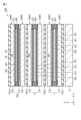
図2は、図1に示した表示装置DSPの一構成例を示す断面図である。
ここに示す第1方向X、第2方向Y、及び、第3方向Zは、互いに直交しているが、90度以外の角度で互いに交差していてもよい。第1方向X及び第2方向Yは、例えば表示装置DSPに含まれる基板に平行な方向に相当し、また、第3方向Zは、表示装置DSPの厚さ方向に相当する。 FIG. 2 is a cross-sectional view showing an example of the configuration of the display device DSP shown in FIG.
The first direction X, the second direction Y, and the third direction Z shown here are mutually orthogonal, but may intersect at an angle other than 90 degrees. The first direction X and the second direction Y correspond to, for example, a direction parallel to a substrate included in the display device DSP, and the third direction Z corresponds to a thickness direction of the display device DSP.
第1視野角制御パネル1は、例えば液晶パネルであり、第1基板SUB1と、第2基板SUB2と、第1液晶層LC1と、を備えている。第1液晶層LC1は、第1基板SUB1と第2基板SUB2との間に保持され、シールSE1によって封止されている。第1液晶層LC1は、後述するように、ハイブリッド配向した液晶分子を含んでいる。The first viewing
第1基板SUB1は、絶縁基板10と、第1透明電極TE1と、第1配向膜AL1と、を備えている。第1透明電極TE1は、視野角を制御するための有効領域AA1において、ほぼ全域に亘って形成され、絶縁基板10と第1配向膜AL1との間に設けられている。The first substrate SUB1 includes an
第2基板SUB2は、第1基板SUB1の前面側に位置している。第2基板SUB2は、絶縁基板20と、第2透明電極TE2と、第2配向膜AL2と、を備えている。第2透明電極TE2は、有効領域AA1において、ほぼ全域に亘って形成され、絶縁基板20と第2配向膜AL2との間に設けられている。The second substrate SUB2 is located on the front side of the first substrate SUB1. The second substrate SUB2 includes an
第1配向膜AL1及び第2配向膜AL2は、第1液晶層LC1に接触している。これらの第1配向膜AL1及び第2配向膜AL2のうちの一方は水平配向膜であり、他方は垂直配向膜である。水平配向膜とは、第1方向X及び第2方向Yによって規定されるX-Y平面に略平行な配向規制力を有する配向膜である。垂直配向膜とは、X-Y平面に略垂直な配向規制力を有する配向膜である。The first alignment film AL1 and the second alignment film AL2 are in contact with the first liquid crystal layer LC1. One of the first alignment film AL1 and the second alignment film AL2 is a horizontal alignment film, and the other is a vertical alignment film. The horizontal alignment film is an alignment film that has an alignment regulation force that is approximately parallel to the X-Y plane defined by the first direction X and the second direction Y. The vertical alignment film is an alignment film that has an alignment regulation force that is approximately perpendicular to the X-Y plane.
第1透明電極TE1は、第3方向Zにおいて、第1液晶層LC1を介して第2透明電極TE2に重畳している。第1透明電極TE1及び第2透明電極TE2は、第1液晶層LC1に電圧を印加するように制御される。The first transparent electrode TE1 overlaps the second transparent electrode TE2 via the first liquid crystal layer LC1 in the third direction Z. The first transparent electrode TE1 and the second transparent electrode TE2 are controlled to apply a voltage to the first liquid crystal layer LC1.
第2視野角制御パネル2は、例えば液晶パネルであり、第3基板SUB3と、第4基板SUB4と、第2液晶層LC2と、を備えている。第2液晶層LC2は、第3基板SUB3と第4基板SUB4との間に保持され、シールSE2によって封止されている。第2液晶層LC2は、後述するように、ハイブリッド配向した液晶分子を含んでいる。The second viewing
第3基板SUB3は、絶縁基板30と、第3透明電極TE3と、第3配向膜AL3と、を備えている。第3透明電極TE3は、視野角を制御するための有効領域AA2において、ほぼ全域に亘って形成され、絶縁基板30と第3配向膜AL3との間に設けられている。The third substrate SUB3 includes an insulating
第4基板SUB4は、第3基板SUB3の前面側に位置している。第4基板SUB4は、絶縁基板40と、第4透明電極TE4と、第4配向膜AL4と、を備えている。第4透明電極TE4は、有効領域AA2において、ほぼ全域に亘って形成され、絶縁基板40と第4配向膜AL4との間に設けられている。The fourth substrate SUB4 is located on the front side of the third substrate SUB3. The fourth substrate SUB4 includes an insulating
第3配向膜AL3及び第4配向膜AL4は、第2液晶層LC2に接触している。これらの第3配向膜AL3及び第4配向膜AL4のうちの一方は水平配向膜であり、他方は垂直配向膜である。第1構成例において、第2視野角制御パネル2における水平配向膜の配向処理方向は、第1視野角制御パネル1における水平配向膜の配向処理方向と平行である。The third alignment film AL3 and the fourth alignment film AL4 are in contact with the second liquid crystal layer LC2. One of the third alignment film AL3 and the fourth alignment film AL4 is a horizontal alignment film, and the other is a vertical alignment film. In the first configuration example, the alignment treatment direction of the horizontal alignment film in the second viewing
第3透明電極TE3は、第3方向Zにおいて、第2液晶層LC2を介して第4透明電極TE4に重畳している。第3透明電極TE3及び第4透明電極TE4は、第2液晶層LC2に電圧を印加するように制御される。The third transparent electrode TE3 overlaps the fourth transparent electrode TE4 via the second liquid crystal layer LC2 in the third direction Z. The third transparent electrode TE3 and the fourth transparent electrode TE4 are controlled to apply a voltage to the second liquid crystal layer LC2.
第1透明電極TE1、第2透明電極TE2、第3透明電極TE3、及び、第4透明電極TE4の各々は、例えば単一のシート状電極であるが、第1方向X及び第2方向Yの少なくとも一方に沿って複数個に分割された電極であってもよい。Each of the first transparent electrode TE1, the second transparent electrode TE2, the third transparent electrode TE3, and the fourth transparent electrode TE4 is, for example, a single sheet-like electrode, but may also be an electrode divided into multiple pieces along at least one of the first direction X and the second direction Y.
上記の第1視野角制御パネル1及び第2視野角制御パネル2は、透過率の低下を抑制する観点で、遮光層及びカラーフィルタ層を備えていない。The above-mentioned first viewing
表示パネルPNLは、例えば液晶パネルであり、第5基板SUB5と、第6基板SUB6と、液晶層LC3、を備えている。液晶層LC3は、第5基板SUB5と第6基板SUB6との間に保持され、シールSE3によって封止されている。ここで説明する表示パネルPNLは、一例として、基板主面に沿った電界によって液晶層LC3に含まれる液晶分子の配向状態を制御するように構成されている。なお、本実施形態の表示パネルPNLは、図示した例に限らず、基板主面の法線に沿った電界によって液晶分子の配向状態を制御するように構成されていてもよい。ここでの基板主面とは、X-Y平面に相当する。The display panel PNL is, for example, a liquid crystal panel, and includes a fifth substrate SUB5, a sixth substrate SUB6, and a liquid crystal layer LC3. The liquid crystal layer LC3 is held between the fifth substrate SUB5 and the sixth substrate SUB6, and is sealed by a seal SE3. The display panel PNL described here is configured, as an example, to control the alignment state of the liquid crystal molecules contained in the liquid crystal layer LC3 by an electric field along the main surfaces of the substrates. Note that the display panel PNL of this embodiment is not limited to the example shown in the figure, and may be configured to control the alignment state of the liquid crystal molecules by an electric field along the normal to the main surfaces of the substrates. The main surfaces of the substrates here correspond to the X-Y plane.
第5基板SUB5は、絶縁基板50と、絶縁膜51と、共通電極CEと、複数の画素電極PEと、配向膜AL5と、を備えている。共通電極CEは、絶縁基板50と絶縁膜51との間に設けられている。複数の画素電極PEは、絶縁膜51と配向膜AL5との間に設けられている。画像を表示する表示領域DAにおいて、複数の画素電極PEは、絶縁膜51を介して1つの共通電極CEに重畳している。画素電極PE及び共通電極CEは、液晶層LC3に電圧を印加するように制御される。なお、ここでは、主要部のみを簡素化して図示しているが、第5基板SUB5は、さらに、複数の走査線、複数の信号線、各画素電極PEと電気的に接続されるスイッチング素子、各種絶縁膜などを備えている。The fifth substrate SUB5 includes an insulating
第6基板SUB6は、第5基板SUB5の前面側に位置している。第6基板SUB6は、絶縁基板60と、配向膜AL6と、を備えている。なお、ここでは、主要部のみを簡素化して図示しているが、第6基板SUB6は、さらに、遮光層、カラーフィルタ層、オーバーコート層、スペーサなどを備えている。The sixth substrate SUB6 is located on the front side of the fifth substrate SUB5. The sixth substrate SUB6 includes an insulating
配向膜AL5及び配向膜AL6は、液晶層LC3に接触している。これらの配向膜AL5及び配向膜AL6は、一例では双方が水平配向膜であるが、双方が垂直配向膜であってもよいし、一方が水平配向膜であって他方が垂直配向膜であってもよい。The alignment films AL5 and AL6 are in contact with the liquid crystal layer LC3. In one example, both of these alignment films AL5 and AL6 are horizontal alignment films, but both may be vertical alignment films, or one may be a horizontal alignment film and the other a vertical alignment film.
ここで、第1視野角制御パネル1と、第2視野角制御パネル2と、表示パネルPNLとの関係に着目する。
第1液晶層LC1、第2液晶層LC2、及び、液晶層LC3は、第3方向Zにおいて互いに重畳している。有効領域AA1、有効領域AA2、及び、表示領域DAは、第3方向Zにおいて互いに重畳している。共通電極CE、複数の画素電極PE、第1透明電極TE1、第2透明電極TE2、第3透明電極TE3、及び、第4透明電極TE4は、第3方向Zにおいて互いに重畳している。 Here, attention is focused on the relationship between the first viewing
The first liquid crystal layer LC1, the second liquid crystal layer LC2, and the liquid crystal layer LC3 overlap each other in the third direction Z. The effective area AA1, the effective area AA2, and the display area DA overlap each other in the third direction Z. The common electrode CE, the multiple pixel electrodes PE, the first transparent electrode TE1, the second transparent electrode TE2, the third transparent electrode TE3, and the fourth transparent electrode TE4 overlap each other in the third direction Z.
絶縁基板10、20、30、40、50、60は、例えばガラス基板や樹脂基板などの透明基板である。なお、これらの6枚の絶縁基板のうちの一部の基板が他の基板とは異なる材料で形成されていてもよい。例えば、絶縁基板10、20、30、40が樹脂基板であり、絶縁基板50及び60がガラス基板であってもよい。The insulating
共通電極CE、画素電極PE、第1透明電極TE1、第2透明電極TE2、第3透明電極TE3、及び、第4透明電極TE4は、インジウム錫酸化物(ITO)やインジウム亜鉛酸化物(IZO)などの透明導電材料によって形成された透明電極である。The common electrode CE, the pixel electrode PE, the first transparent electrode TE1, the second transparent electrode TE2, the third transparent electrode TE3, and the fourth transparent electrode TE4 are transparent electrodes formed from a transparent conductive material such as indium tin oxide (ITO) or indium zinc oxide (IZO).
第1偏光板POL1は、絶縁基板10に接着されている。第2偏光板POL2は、絶縁基板20及び絶縁基板30の少なくとも一方に接着されている。第3偏光板POL3は、絶縁基板40に接着されている。第4偏光板POL4は、絶縁基板60に接着されている。これらの第1乃至第5偏光板POL1乃至POL5は、予め成形されたフィルムの片面に粘着剤を有するものであるが、絶縁基板の表面に直接形成されてもよい。The first polarizing plate POL1 is adhered to the insulating
このような表示装置DSPにおいて、照明装置ILから出射された照明光(無偏光)は、第3方向Zに沿って進行し、第1視野角制御パネル1及び第2視野角制御パネル2を順次透過した後に、表示パネルPNLを照明する。In such a display device DSP, the illumination light (unpolarized) emitted from the illumination device IL travels along the third direction Z, sequentially passes through the first viewing
より具体的には、照明装置ILから出射された照明光が無偏光である場合、第1偏光板POL1は、照明光の一部の偏光成分を透過する。
第1視野角制御パネル1は、第1液晶層LC1において、第1偏光板POL1を透過した偏光成分を変調して透過する。第2偏光板POL2は、第1視野角制御パネル1を透過した偏光成分を透過する。
第2視野角制御パネル2は、第2液晶層LC2において、第2偏光板POL2を透過した偏光成分を変調して透過する。第3偏光板POL3は、第2視野角制御パネル2を透過した偏光成分を透過する。
表示パネルPNLは、第3偏光板POL3を透過した偏光成分によって照明され、液晶層LC3において偏光成分を変調する。第4偏光板POL4は、表示パネルPNLを透過した偏光成分の少なくとも一部を透過する。
ここで説明した偏光成分は、X-Y平面に偏光軸を有する直線偏光である。 More specifically, when the illumination light emitted from the illumination device IL is unpolarized, the first polarizer POL1 transmits a portion of the polarized component of the illumination light.
The first viewing
The second viewing
The display panel PNL is illuminated by the polarized light component that has passed through the third polarizer POL3, and the polarized light component is modulated in the liquid crystal layer LC3. The fourth polarizer POL4 transmits at least a part of the polarized light component that has passed through the display panel PNL.
The polarized light components described here are linearly polarized light with their polarization axis in the XY plane.
図3は、図1に示した表示装置DSPを構成する各光学要素の軸角度を説明するための図である。
ここでは、X-Y平面内において、第1方向X(X軸)を示す矢印の先端の方位を基準方位とし、基準方位に対して反時計回りの角度を正の角度とする。 FIG. 3 is a diagram for explaining the axial angles of the optical elements constituting the display device DSP shown in FIG.
Here, in the XY plane, the direction of the tip of the arrow indicating the first direction X (X-axis) is defined as the reference direction, and a counterclockwise angle with respect to the reference direction is defined as a positive angle.
第1偏光板POL1は、第1透過軸T1を有している。第2偏光板POL2は、第2透過軸T2を有している。第3偏光板POL3は、互いにほぼ直交する第3吸収軸A3及び第3透過軸T3を有している。第4偏光板POL4は、互いにほぼ直交する第4吸収軸A4及び第4透過軸T4を有している。
なお、図示を省略するが、第1偏光板POL1の第1吸収軸は第1透過軸T1にほぼ直交し、第2偏光板POL2の第2吸収軸は第2透過軸T2にほぼ直交している。 The first polarizer POL1 has a first transmission axis T1. The second polarizer POL2 has a second transmission axis T2. The third polarizer POL3 has a third absorption axis A3 and a third transmission axis T3 that are substantially perpendicular to each other. The fourth polarizer POL4 has a fourth absorption axis A4 and a fourth transmission axis T4 that are substantially perpendicular to each other.
Although not shown, the first absorption axis of the first polarizing plate POL1 is substantially perpendicular to the first transmission axis T1, and the second absorption axis of the second polarizing plate POL2 is substantially perpendicular to the second transmission axis T2.
表示パネルPNLを挟む第3偏光板POL3及び第4偏光板POL4のそれぞれの透過軸は、互いに直交している。例えば、第4吸収軸A4は、第1方向Xにほぼ平行であり、0°の方位に位置している。第4透過軸T4は、90°の方位に位置している。第3吸収軸A3は、第4吸収軸A4にほぼ直交し、90°の方位に位置している。第3透過軸T3は、第4透過軸T4にほぼ直交し、0°の方位に位置している。The transmission axes of the third polarizer POL3 and the fourth polarizer POL4, which sandwich the display panel PNL, are perpendicular to each other. For example, the fourth absorption axis A4 is nearly parallel to the first direction X and is located at an orientation of 0°. The fourth transmission axis T4 is located at an orientation of 90°. The third absorption axis A3 is nearly perpendicular to the fourth absorption axis A4 and is located at an orientation of 90°. The third transmission axis T3 is nearly perpendicular to the fourth transmission axis T4 and is located at an orientation of 0°.
第1視野角制御パネル1を挟む第1偏光板POL1及び第2偏光板POL2のそれぞれの透過軸は、互いに平行である。また、第2視野角制御パネル2を挟む第2偏光板POL2及び第3偏光板POL3のそれぞれの透過軸は、互いに平行である。つまり、第1透過軸T1、第2透過軸T2、及び、第3透過軸T3は、互いに平行であり、いずれも0°の方位に位置している。The transmission axes of the first polarizer POL1 and the second polarizer POL2 that sandwich the first viewing
第1視野角制御パネル1における水平配向膜の配向処理方向AD1、及び、第2視野角制御パネル2における水平配向膜の配向処理方向AD2は、互いに平行である。図3に示す例では、配向処理方向AD1及びAD2は、第1透過軸T1、第2透過軸T2、及び、第3透過軸T3に直交している。つまり、配向処理方向AD1及びAD2は、90°の方位に位置している。
なお、配向処理方向AD1及びAD2は、第1透過軸T1、第2透過軸T2、及び、第3透過軸T3に平行であってもよい。この場合、配向処理方向AD1及びAD2は、0°の方位に位置している。 The alignment treatment direction AD1 of the horizontal alignment film in the first viewing
The alignment directions AD1 and AD2 may be parallel to the first transmission axis T1, the second transmission axis T2, and the third transmission axis T3. In this case, the alignment directions AD1 and AD2 are located at an azimuth of 0°.
また、第1透過軸T1、第2透過軸T2、及び、第3透過軸T3が90°の方位に位置し、配向処理方向AD1及びAD2が0°の方位または90°の方位に位置していてもよい。In addition, the first transmission axis T1, the second transmission axis T2, and the third transmission axis T3 may be located at an orientation of 90°, and the alignment directions AD1 and AD2 may be located at an orientation of 0° or 90°.
ここでの0°の方位とはX-Y平面における0°-180°に亘る方位に相当し、90°の方位とは90°-270°に亘る方位に相当する。Here, the 0° orientation corresponds to an orientation ranging from 0°-180° on the XY plane, and the 90° orientation corresponds to an orientation ranging from 90°-270°.
このような表示装置DSPにおいて、第3方向Zに沿って光が進行する場合、第1偏光板POL1を透過した直線偏光は第1透過軸T1に沿った第1偏光軸を有し、第1視野角制御パネル1を経て第2偏光板POL2を透過した直線偏光は第2透過軸T2に沿った第2偏光軸を有している。第2偏光板POL2を透過した後に第2視野角制御パネル2を透過した直線偏光は、第3透過軸T3に沿った第3偏光軸を有している。In such a display device DSP, when light travels along the third direction Z, the linearly polarized light transmitted through the first polarizer POL1 has a first polarization axis along the first transmission axis T1, and the linearly polarized light transmitted through the first viewing
上記の通り、第1透過軸T1、第2透過軸T2、及び、第3透過軸T3が互いに平行であるため、光が電子機器100を透過する過程で、直線偏光の偏光軸は同一方向に維持される。図3に示す例では、第1偏光軸、第2偏光軸、及び、第3偏光軸は、互いに平行であり、いずれも0°の方位(あるいは、0°-180°の方位、または、第1方向X)に位置している。As described above, since the first transmission axis T1, the second transmission axis T2, and the third transmission axis T3 are parallel to each other, the polarization axis of the linearly polarized light is maintained in the same direction as the light passes through the
第3偏光板POL3を透過した直線偏光は、表示パネルPNLを照明する。表示パネルPNLを照明する直線偏光は、液晶層LC3において適宜変調され、その少なくとも一部が第4偏光板POL4を透過することで画面(X-Y平面と平行な面)に画像を形成する。第4偏光板POL4を透過した直線偏光は、第4透過軸T4に沿った偏光軸を有している。つまり、第4偏光板POL4を透過した直線偏光の偏光軸は、90°の方位(あるいは、90°-270°の方位)に位置している。The linearly polarized light that has passed through the third polarizer POL3 illuminates the display panel PNL. The linearly polarized light that illuminates the display panel PNL is appropriately modulated in the liquid crystal layer LC3, and at least a portion of it passes through the fourth polarizer POL4 to form an image on the screen (a surface parallel to the X-Y plane). The linearly polarized light that has passed through the fourth polarizer POL4 has a polarization axis that is aligned with the fourth transmission axis T4. In other words, the polarization axis of the linearly polarized light that has passed through the fourth polarizer POL4 is located in an orientation of 90° (or an orientation of 90°-270°).
電子機器100と表示パネルPNLとを重ね合わせる際、画面内の水平方向を第1方向Xとし、画面内の垂直方向を第2方向Yとし、画面の法線方向を第3方向Zとしたとき、配向処理方向AD1及びAD2は、第2方向Yに平行となるように設定される。図示したX-Y平面において、0°-180°の方位は画面内の水平方向(あるいは画面内の左右方向)に相当し、90°-270°の方位は画面内の垂直方向(あるいは画面内の上下方向)に相当する。When the
一般的な偏光サングラスの吸収軸は、第4偏光板POL4の第4吸収軸A4と平行であるため、偏光サングラスを介して表示装置DSPを観察した場合であっても、画面に表示された画像を視認することができる。The absorption axis of typical polarized sunglasses is parallel to the fourth absorption axis A4 of the fourth polarizer POL4, so the image displayed on the screen can be seen even when observing the display device DSP through polarized sunglasses.
次に、第1視野角制御パネル1及び第2視野角制御パネル2について説明する。
図4は、第1視野角制御パネル1及び第2視野角制御パネル2の一構成例を説明するための図である。
ここでは、第1液晶層LC1に電圧が印加されていないオフ時の液晶分子LM1の初期配向状態、及び、第2液晶層LC2に電圧が印加されていないオフ時の液晶分子LM2の初期配向状態を示している。また、ここに示す例では、第1配向膜AL1及び第3配向膜AL3が垂直配向膜であり、第2配向膜AL2及び第4配向膜AL4が水平配向膜である場合について説明する。但し、第1配向膜AL1及び第3配向膜AL3が水平配向膜であり、第2配向膜AL2及び第4配向膜AL4が垂直配向膜であってもよい。 Next, the first viewing
FIG. 4 is a diagram for explaining an example of the configuration of the first viewing
Here, the initial alignment state of the liquid crystal molecules LM1 in the off state when no voltage is applied to the first liquid crystal layer LC1, and the initial alignment state of the liquid crystal molecules LM2 in the off state when no voltage is applied to the second liquid crystal layer LC2 are shown. In the example shown here, the first alignment film AL1 and the third alignment film AL3 are vertical alignment films, and the second alignment film AL2 and the fourth alignment film AL4 are horizontal alignment films. However, the first alignment film AL1 and the third alignment film AL3 may be horizontal alignment films, and the second alignment film AL2 and the fourth alignment film AL4 may be vertical alignment films.
水平配向膜である第2配向膜AL2及び第4配向膜AL4に対しては配向処理が必要であり、垂直配向膜である第1配向膜AL1及び第3配向膜AL3に対しては配向処理が不要である。但し、安定な配向状態を得る観点では、第1配向膜AL1及び第3配向膜AL3に対して配向処理を行うことが望ましい。この場合、第1配向膜AL1の配向処理方向AD11及び第3配向膜AL3の配向処理方向AD21は、第2配向膜AL2の配向処理方向AD1及び第4配向膜AL4の配向処理方向AD2にほぼ平行であり、且つ、逆向きである。なお、配向処理とは、ラビング処理であってもよいし、光配向処理であってもよい。The second alignment film AL2 and the fourth alignment film AL4, which are horizontal alignment films, require alignment treatment, whereas the first alignment film AL1 and the third alignment film AL3, which are vertical alignment films, do not require alignment treatment. However, from the viewpoint of obtaining a stable alignment state, it is desirable to perform alignment treatment on the first alignment film AL1 and the third alignment film AL3. In this case, the alignment treatment direction AD11 of the first alignment film AL1 and the alignment treatment direction AD21 of the third alignment film AL3 are substantially parallel to and opposite to the alignment treatment direction AD1 of the second alignment film AL2 and the alignment treatment direction AD2 of the fourth alignment film AL4. The alignment treatment may be a rubbing treatment or a photo-alignment treatment.
図4に示す構成例では、配向処理方向AD1及び配向処理方向AD2は、90°の方位に位置し、配向処理方向AD11及び配向処理方向AD21は、270°の方位に位置している。In the configuration example shown in FIG. 4, the alignment process direction AD1 and the alignment process direction AD2 are positioned at an orientation of 90°, and the alignment process direction AD11 and the alignment process direction AD21 are positioned at an orientation of 270°.
第1液晶層LC1において、第1配向膜AL1と第2配向膜AL2との間で第3方向Zに沿って並んだ複数の液晶分子LM1は、ハイブリッド配向している。なお、図4では、平面視における複数の液晶分子LM1を模式的に示している。第1基板SUB1に近接する側の液晶分子LMAは、その長軸が基板の法線(第3方向)に沿うように垂直配向している。In the first liquid crystal layer LC1, multiple liquid crystal molecules LM1 aligned along the third direction Z between the first alignment film AL1 and the second alignment film AL2 are hybrid aligned. Note that FIG. 4 shows multiple liquid crystal molecules LM1 in a planar view. The liquid crystal molecules LMA on the side closest to the first substrate SUB1 are vertically aligned with their major axes aligned along the normal (third direction) of the substrate.
第2基板SUB2に近接する側の液晶分子(第1液晶分子)LMBは、X-Y平面に沿って水平配向しており、その長軸が配向処理方向AD1に沿うように初期配向している。あるいは、液晶分子LMBの第1初期配向方向は、配向処理方向AD1に平行であり、第1透過軸T1に直交している。つまり、液晶分子LMBは、90°-270°の方位(あるいは画面内の垂直方向)に初期配向している。しかも、液晶分子LMBは、配向処理方向AD1を示す矢印の先端側の端部が第2基板SUB2から離間するように傾斜している(あるいは、配向処理方向AD1を示す矢印の後端側の端部が第2基板SUB2に近接するように傾斜している)。The liquid crystal molecules (first liquid crystal molecules) LMB on the side close to the second substrate SUB2 are horizontally aligned along the X-Y plane, and are initially aligned so that their major axes are aligned along the alignment treatment direction AD1. Alternatively, the first initial alignment direction of the liquid crystal molecules LMB is parallel to the alignment treatment direction AD1 and perpendicular to the first transmission axis T1. In other words, the liquid crystal molecules LMB are initially aligned in the 90°-270° direction (or the vertical direction in the screen). Moreover, the liquid crystal molecules LMB are inclined so that the end on the tip side of the arrow indicating the alignment treatment direction AD1 is away from the second substrate SUB2 (or the end on the rear end side of the arrow indicating the alignment treatment direction AD1 is inclined so that the end close to the second substrate SUB2).
なお、配向処理方向AD1を示す矢印、及び、配向処理方向AD11を示す矢印がそれぞれ逆向きであってもよい。また、第1配向膜AL1が水平配向膜であって第2配向膜AL2が垂直配向膜である場合には、液晶分子LMAが90°-270°の方位に水平配向し、液晶分子LMBが垂直配向している。The arrow indicating the alignment direction AD1 and the arrow indicating the alignment direction AD11 may point in opposite directions. In addition, when the first alignment film AL1 is a horizontal alignment film and the second alignment film AL2 is a vertical alignment film, the liquid crystal molecules LMA are horizontally aligned in the 90°-270° direction, and the liquid crystal molecules LMB are vertically aligned.
第2液晶層LC2において、第3配向膜AL3と第4配向膜AL4との間で第3方向Zに沿って並んだ複数の液晶分子LM2は、ハイブリッド配向している。なお、図4では、平面視における複数の液晶分子LM2を模式的に示している。第3基板SUB3に近接する側の液晶分子LMCは、その長軸が基板の法線(第3方向)に沿うように垂直配向している。In the second liquid crystal layer LC2, the liquid crystal molecules LM2 aligned along the third direction Z between the third alignment film AL3 and the fourth alignment film AL4 are hybrid aligned. Note that FIG. 4 shows the liquid crystal molecules LM2 in a plan view. The liquid crystal molecules LMC on the side closest to the third substrate SUB3 are vertically aligned with their major axes aligned along the normal (third direction) of the substrate.
第4基板SUB4に近接する側の液晶分子(第2液晶分子)LMDは、X-Y平面に沿って水平配向しており、その長軸が配向処理方向AD2に沿うように初期配向している。あるいは、液晶分子LMDの第2初期配向方向は、配向処理方向AD2に平行であり、第1透過軸T1に直交している。つまり、液晶分子LMDは、90°-270°の方位(あるいは画面内の垂直方向)に初期配向している。しかも、液晶分子LMDは、配向処理方向AD2を示す矢印の先端側の端部が第4基板SUB4から離間するように傾斜している(あるいは、配向処理方向AD2を示す矢印の後端側の端部が第4基板SUB4に近接するように傾斜している)。The liquid crystal molecules (second liquid crystal molecules) LMD on the side close to the fourth substrate SUB4 are aligned horizontally along the X-Y plane, and are initially aligned so that their major axes are aligned along the alignment treatment direction AD2. Alternatively, the second initial alignment direction of the liquid crystal molecules LMD is parallel to the alignment treatment direction AD2 and perpendicular to the first transmission axis T1. In other words, the liquid crystal molecules LMD are initially aligned in the 90°-270° direction (or the vertical direction in the screen). Moreover, the liquid crystal molecules LMD are inclined so that the end on the tip side of the arrow indicating the alignment treatment direction AD2 is away from the fourth substrate SUB4 (or the end on the rear side of the arrow indicating the alignment treatment direction AD2 is inclined so that the end close to the fourth substrate SUB4).
なお、配向処理方向AD2を示す矢印、及び、配向処理方向AD21を示す矢印がそれぞれ逆向きであってもよい。また、第3配向膜AL3が水平配向膜であって第4配向膜AL4が垂直配向膜である場合には、液晶分子LMCが90°-270°の方位に水平配向し、液晶分子LMDが垂直配向している。The arrow indicating the alignment process direction AD2 and the arrow indicating the alignment process direction AD21 may point in opposite directions. In addition, when the third alignment film AL3 is a horizontal alignment film and the fourth alignment film AL4 is a vertical alignment film, the liquid crystal molecules LMC are horizontally aligned in the 90°-270° direction, and the liquid crystal molecules LMD are vertically aligned.
このように、第1液晶層LC1の液晶分子のうちの水平配向した液晶分子LMBの第1初期配向方向、及び、第2液晶層LC2の液晶分子のうちの水平配向した液晶分子LMDの第2初期配向方向は、互いに平行であり、且つ、第1透過軸T1、第2透過軸T2、第3透過軸T3と直交している。In this way, the first initial alignment direction of the horizontally aligned liquid crystal molecules LMB of the first liquid crystal layer LC1 and the second initial alignment direction of the horizontally aligned liquid crystal molecules LMD of the second liquid crystal layer LC2 are parallel to each other and perpendicular to the first transmission axis T1, the second transmission axis T2, and the third transmission axis T3.
なお、配向処理方向AD1及びAD2が0°の方位に位置していてもよく、この場合には、液晶分子LMBの第1初期配向方向、及び、液晶分子LMDの第2初期配向方向は、互いに平行であり、且つ、第1透過軸T1、第2透過軸T2、第3透過軸T3と平行である。The alignment directions AD1 and AD2 may be oriented at 0°. In this case, the first initial alignment direction of the liquid crystal molecules LMB and the second initial alignment direction of the liquid crystal molecules LMD are parallel to each other and to the first transmission axis T1, the second transmission axis T2, and the third transmission axis T3.
図5は、第1視野角制御パネル1の動作を説明するための図である。
図の左側に示す断面図は第1透明電極TE1と第2透明電極TE2の間に電位差が生じていないオフ状態(OFF)を示し、図の右側に示す断面図は第1透明電極TE1と第2透明電極TE2の間に電位差が生じているオン状態(ON)を示している。 FIG. 5 is a diagram for explaining the operation of the first viewing
The cross-sectional view shown on the left side of the figure shows the off state (OFF) in which no potential difference occurs between the first transparent electrode TE1 and the second transparent electrode TE2, and the cross-sectional view shown on the right side of the figure shows the on state (ON) in which a potential difference occurs between the first transparent electrode TE1 and the second transparent electrode TE2.
第1液晶層LC1は、負の誘電率異方性を有する液晶材料(ネガ型液晶材料)によって形成されている。図5には示していないが、第2視野角制御パネル2の第2液晶層LC2も、ネガ型液晶材料によって形成されている。第3方向Zに沿って配列した複数の液晶分子LM1は、液晶分子LMA及びLMBを含んでいる。オフ状態では、第1配向膜AL1の近傍の液晶分子LMAはほぼ垂直配向を呈し、第2配向膜AL2の近傍の液晶分子LMBはほぼ水平配向を呈する。また、液晶分子LMAと液晶分子LMBとの間の他の液晶分子LM1は、それぞれのチルト角が連続的に変化している。このように、複数の液晶分子LM1は、ハイブリッド配向を呈するように初期配向している。
オン状態では、ネガ型液晶材料については、液晶分子LM1の長軸は、電界と交差するように配向する。つまり、液晶分子LM1は、それぞれ水平配向している。 The first liquid crystal layer LC1 is made of a liquid crystal material having a negative dielectric anisotropy (negative liquid crystal material). Although not shown in FIG. 5, the second liquid crystal layer LC2 of the second viewing
In the on-state, for a negative type liquid crystal material, the long axes of the liquid crystal molecules LM1 are aligned across the electric field, i.e., the liquid crystal molecules LM1 are each horizontally aligned.
ここでは、第1視野角制御パネル1として、第1液晶層LC1がネガ型液晶材料によって形成された場合について説明したが、第1液晶層LC1が正の誘電率異方性を有するポジ型液晶材料によって形成されてもよい。また、第1視野角制御パネル1は、電界制御複屈折モードを適用した液晶パネルであってもよい。この場合も、第1配向膜AL1の配向処理方向AD11、及び、第2配向膜AL2の配向処理方向AD1は、互いに平行であり、且つ、逆向きであって、90°-270°の方位に位置するように設定される。Here, the first viewing
図5では、第1視野角制御パネル1の動作について説明したが、第2視野角制御パネル2の動作も第1視野角制御パネル1の動作と実質的に同一であり、説明を省略する。In Figure 5, the operation of the first viewing
次に、表示パネルPNLについて説明する。
図6は、表示パネルPNLにおける画素レイアウトの一例を示す平面図である。
ここでは、説明に必要な構成のみを図示している。第5基板SUB5は、複数の走査線Gと、複数の信号線Sと、複数のスイッチング素子SWと、複数の画素電極PE1及びPE2と、共通電極CEと、を備えている。 Next, the display panel PNL will be described.
FIG. 6 is a plan view showing an example of a pixel layout in the display panel PNL.
Here, only the configuration necessary for explanation is shown. The fifth substrate SUB5 includes a plurality of scanning lines G, a plurality of signal lines S, a plurality of switching elements SW, a plurality of pixel electrodes PE1 and PE2, and a common electrode CE.
複数の走査線Gは、それぞれ第1方向Xに沿って直線的に延出し、第2方向Yに間隔をおいて並んでいる。複数の信号線Sは、それぞれ概ね第2方向Yに沿って延出し、第1方向Xに間隔をおいて並んでいる。スイッチング素子SWは、いずれかの走査線G及びいずれかの信号線Sと電気的に接続されている。画素電極PE1及びPE2の各々は、いずれかのスイッチング素子SWと電気的に接続されている。The multiple scanning lines G each extend linearly along the first direction X and are arranged at intervals in the second direction Y. The multiple signal lines S each extend roughly along the second direction Y and are arranged at intervals in the first direction X. The switching element SW is electrically connected to any of the scanning lines G and any of the signal lines S. Each of the pixel electrodes PE1 and PE2 is electrically connected to any of the switching elements SW.
複数の画素電極PE1は、第1方向Xに沿って並んでいる。画素電極PE1は、共通電極CEに重畳する帯電極Pa1を有している。帯電極Pa1は、第1方向X及び第2方向Yとは異なる方向D1に沿って延出している。
複数の画素電極PE2は、第1方向Xに沿って並んでいる。画素電極PE2は、共通電極CEに重畳する帯電極Pa2を有している。帯電極Pa2は、方向D1とは異なる方向D2に沿って延出している。なお、帯電極Pa1及びPa2の本数は、1本でもよいし、3本以上であってもよい。 The pixel electrodes PE1 are arranged in a first direction X. Each pixel electrode PE1 has a charging electrode Pa1 overlapping a common electrode CE. The charging electrode Pa1 extends in a direction D1 different from the first direction X and the second direction Y.
The pixel electrodes PE2 are arranged along the first direction X. The pixel electrodes PE2 have a charging electrode Pa2 overlapping the common electrode CE. The charging electrode Pa2 extends along a direction D2 different from the direction D1. The number of charging electrodes Pa1 and Pa2 may be one or three or more.
図7は、表示パネルPNLの一構成例を説明するための図である。
ここでは、配向膜AL5と配向膜AL6との間の液晶層LC3に電圧が印加されていないオフ時の液晶分子LMの初期配向状態を示している。 FIG. 7 is a diagram for explaining an example of the configuration of the display panel PNL.
Here, the initial alignment state of the liquid crystal molecules LM at the off time when no voltage is applied to the liquid crystal layer LC3 between the alignment films AL5 and AL6 is shown.
配向膜AL5の配向処理方向AD5、及び、配向膜AL6の配向処理方向AD6は、ほぼ平行であり、互いに逆向きである。配向処理方向AD5及び配向処理方向AD6は、例えば第4透過軸T4とほぼ平行である。つまり、X-Y平面において、配向処理方向AD5を示す矢印の先端は90°の方位に位置し、配向処理方向AD6を示す矢印の先端は270°の方位に位置している。液晶層LC3において、第3方向Zに沿って並んだ複数の液晶分子LM3は、ホモジニアス配向している。液晶分子LM3は、その長軸が第2方向Yに沿うように配向している。The alignment process direction AD5 of the alignment film AL5 and the alignment process direction AD6 of the alignment film AL6 are substantially parallel and opposite to each other. The alignment process direction AD5 and the alignment process direction AD6 are, for example, substantially parallel to the fourth transmission axis T4. That is, in the X-Y plane, the tip of the arrow indicating the alignment process direction AD5 is located at an azimuth of 90°, and the tip of the arrow indicating the alignment process direction AD6 is located at an azimuth of 270°. In the liquid crystal layer LC3, multiple liquid crystal molecules LM3 aligned along the third direction Z are homogeneously aligned. The liquid crystal molecules LM3 are aligned so that their major axes are aligned along the second direction Y.
なお、配向処理方向AD5及び配向処理方向AD6は、第4透過軸T4とほぼ直交していてもよい。また、第3透過軸T3が90°の方位に位置し、第4透過軸T4が0°の方位に位置していてもよいが、上記の通り、偏光サングラスを介して表示画像を視認する観点では、図示したように、第4透過軸T4が90°の方位に位置し、第3透過軸T3が0°の方位に位置していることが望ましい。The alignment direction AD5 and the alignment direction AD6 may be substantially perpendicular to the fourth transmission axis T4. The third transmission axis T3 may be located at an orientation of 90° and the fourth transmission axis T4 may be located at an orientation of 0°. However, as described above, from the viewpoint of viewing the display image through polarized sunglasses, it is preferable that the fourth transmission axis T4 is located at an orientation of 90° and the third transmission axis T3 is located at an orientation of 0°, as shown in the figure.
次に、第1構成例の電子機器100の視野角特性について説明する。Next, the viewing angle characteristics of the
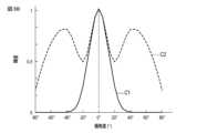
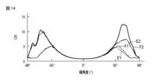
図8Aは、電子機器100におけるオフ時及びオン時の視野角特性を示す図である。
図の横軸は、電子機器100の法線に対する極角度(°)を示し、ここでは、上記のX-Y平面における第1方向X、つまり、0°-180°方位に沿った極角度を示している。X-Y平面における0°の方位(第1方向Xを示す矢印の先端)を正の角度とし、X-Y平面における180°の方位(第1方向Xを示す矢印の後端)を負の角度としている。図の縦軸は、輝度(相対値)を示している。 FIG. 8A is a diagram showing the viewing angle characteristics of
The horizontal axis of the diagram indicates the polar angle (°) with respect to the normal to the
ここで説明するシミュレーションの条件は、以下の通りである。照明装置ILからの照明光は無偏光であり、第1視野角制御パネル1が第1偏光板POL1と第2偏光板POL2とで挟持され、第2視野角制御パネル2が第2偏光板POL2と第3偏光板POL3とで挟持され、その他の光学素子は設けず、オン時における第1液晶層LC1及び第2液晶層LC2の駆動電圧は30Vであり、透過光の波長は550nmである。
第1液晶層LC1及び第2液晶層LC2におけるそれぞれの屈折率異方性Δnは0.15とし、第1液晶層LC1及び第2液晶層LC2のそれぞれの厚さdは30μmとし、第1液晶層LC1及び第2液晶層LC2はそれぞれネガ型液晶材料によって形成されているものとする。
オン時及びオフ時について、それぞれ第3偏光板POL3を透過した光の輝度をシミュレーションにより算出した。 The conditions of the simulation described here are as follows: the illumination light from the illumination device IL is unpolarized, the first viewing
The refractive index anisotropy Δn of each of the first liquid crystal layer LC1 and the second liquid crystal layer LC2 is 0.15, the thickness d of each of the first liquid crystal layer LC1 and the second liquid crystal layer LC2 is 30 μm, and the first liquid crystal layer LC1 and the second liquid crystal layer LC2 are each formed from a negative type liquid crystal material.
The luminance of light transmitted through the third polarizer POL3 when the liquid crystal display device is on and when the liquid crystal display device is off was calculated by simulation.
本実施形態の電子機器100におけるシミュレーション結果を図中のA1及びA2として示す。図中のA1で示すシミュレーション結果はオフ時の視野角特性に相当し、図中のA2で示すシミュレーション結果はオン時の視野角特性に相当する。The simulation results for the
オフ時の視野角特性A1及びオン時の視野角特性A2のいずれも、法線方向から観察した場合(極角度が0°の場合)に、輝度が最大となる。また、視野角特性A1及びA2のいずれにおいても、法線方向に対して0°の方位に観察位置を傾けた場合(すなわち正の極角度の場合)であっても、法線方向に対して180°の方位に観察位置を傾けた場合(すなわち負の極角度の場合)であっても、極角度の増加に伴って輝度が低下する傾向を呈し、輝度分布がほぼ対称となる。For both viewing angle characteristic A1 when off and viewing angle characteristic A2 when on, the luminance is maximum when observed from the normal direction (when the polar angle is 0°). In addition, for both viewing angle characteristics A1 and A2, the luminance tends to decrease as the polar angle increases, whether the observation position is tilted at an azimuth of 0° from the normal direction (i.e., in the case of a positive polar angle) or the observation position is tilted at an azimuth of 180° from the normal direction (i.e., in the case of a negative polar angle), and the luminance distribution becomes nearly symmetrical.
オフ時における高輝度の範囲は、オン時における高輝度の範囲より小さい。例えば、オン時の視野角特性A2に着目すると、極角度が80°であっても、法線方向での輝度に対して15%以上の輝度が得られる。一方、オフ時の視野角特性A1に着目すると、極角度が40°を超えると、法線方向での輝度に対して1%未満の輝度しか得られない。The range of high brightness when the display is off is smaller than the range of high brightness when the display is on. For example, when looking at the viewing angle characteristic A2 when the display is on, even if the polar angle is 80°, a brightness of 15% or more is obtained compared to the brightness in the normal direction. On the other hand, when looking at the viewing angle characteristic A1 when the display is off, when the polar angle exceeds 40°, a brightness of less than 1% is obtained compared to the brightness in the normal direction.
図8Aには、比較例のシミュレーション結果も併せて図示している。
比較例のシミュレーションの条件は、第1視野角制御パネル1が第1偏光板POL1と第2偏光板POL2とで挟持され、第2視野角制御パネル2及び第3偏光板POL3は設けないものとし、その他の条件は上記と同一である。 FIG. 8A also shows the simulation results of a comparative example.
The conditions for the simulation of the comparative example are that the first viewing
比較例の電子機器におけるシミュレーション結果を図中のB1及びB2として示す。図中のB1で示すシミュレーション結果はオフ時の視野角特性に相当し、図中のB2で示すシミュレーション結果はオン時の視野角特性に相当する。オン時の視野角特性B2は、本実施形態の電子機器100おけるオン時の視野角特性A2と同等である。The simulation results for the electronic device of the comparative example are shown as B1 and B2 in the figure. The simulation result shown as B1 in the figure corresponds to the viewing angle characteristics when off, and the simulation result shown as B2 in the figure corresponds to the viewing angle characteristics when on. The viewing angle characteristics B2 when on are equivalent to the viewing angle characteristics A2 when on in the
オフ時の視野角特性B1は、視野角特性A1と比較して、よりブロードな傾向を呈する。すなわち、視野角特性B1に着目すると、極角度が40°の場合に、法線方向での輝度に対して約5%の輝度が得られ、極角度が60°の場合に、法線方向での輝度に対して1%程度の輝度となる。The viewing angle characteristic B1 when off tends to be broader than the viewing angle characteristic A1. In other words, when focusing on the viewing angle characteristic B1, when the polar angle is 40°, the brightness is about 5% of the brightness in the normal direction, and when the polar angle is 60°, the brightness is about 1% of the brightness in the normal direction.
以上のシミュレーション結果から、本実施形態の電子機器100によれば、第1視野角制御パネル1及び第2視野角制御パネル2のオン/オフを制御することにより、高い視野角制御能を実現できることが確認された。From the above simulation results, it was confirmed that the
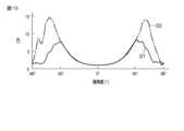
参考までに、第2偏光板POL2が存在する場合と存在しない場合とでのオフ時の視野角特性を比較した。図8Bにオフ時の視野角特性のシミュレーション結果を示す。図中のC1は、第2偏光板POL2が存在する場合(第1構成例に相当)のシミュレーション結果を示し、図中のC2は、第2偏光板POL2が存在しない場合のシミュレーション結果を示している。
図の横軸は極角度(°)を示し、図の縦軸は輝度(相対値)を示している。
視野角特性C2は、視野角特性C1と比較して、よりブロードな傾向を呈することが確認された。すなわち、視野角特性C2に着目すると、極角度が0°から20°まで増加するにしたがって次第に輝度が低下するものの、極角度が20°から50°まで増加するにしたがって再び輝度が増大する傾向が確認された。
これらのシミュレーション結果から、第1構成例においては、第1視野角制御パネル1と第2視野角制御パネル2との間に第2偏光板POL2を配置することが極めて重要であり、そして、第2偏光板POL2の第2透過軸T2を第1透過軸T1及び第3透過軸T3と平行に設定することにより、より高い視野角制御能を実現できることが確認された。 For reference, the viewing angle characteristics when the second polarizer POL2 is present and when it is not present are compared. Figure 8B shows the simulation results of the viewing angle characteristics when the second polarizer POL2 is present (corresponding to the first configuration example), and C2 shows the simulation results when the second polarizer POL2 is not present.
The horizontal axis of the diagram represents the polar angle (°), and the vertical axis of the diagram represents the luminance (relative value).
It was confirmed that the viewing angle characteristic C2 shows a broader tendency than the viewing angle characteristic C1. That is, focusing on the viewing angle characteristic C2, it was confirmed that the luminance gradually decreases as the polar angle increases from 0° to 20°, but the luminance tends to increase again as the polar angle increases from 20° to 50°.
From these simulation results, it was confirmed that in the first configuration example, it is extremely important to place the second polarizing plate POL2 between the first viewing
図9は、図8Aに示したシミュレーション結果に基づくコントラスト比(CR)の計算結果を示す図である。
図の横軸は極角度(°)を示し、図の縦軸はコントラスト比を示している。コントラスト比は、(オン時の輝度/オフ時の輝度)として算出した。 FIG. 9 is a diagram showing the calculation results of the contrast ratio (CR) based on the simulation results shown in FIG. 8A.
The horizontal axis of the figure represents the polar angle (°), and the vertical axis of the figure represents the contrast ratio, which was calculated as (brightness when on/brightness when off).
本実施形態の電子機器100によれば、図中にA3として示すように、極角度が40°の場合に1:100のコントラスト比が得られ、極角度が50°の場合に1:600のコントラスト比が得られた。比較例の電子機器によれば、極角度が80°であっても、コントラスト比は1:100を実現できなかった。As shown by A3 in the figure, the
《第2構成例》
次に、図1に示した表示装置DSPに適用可能な他の電子機器100について説明する。 Second Configuration Example
Next, another
図10は、図1に示した表示装置DSPを構成する各光学要素の軸角度を説明するための図である。
図10に示す第2構成例は、図3に示した第1構成例と比較して、第1視野角制御パネル1の配向処理方向AD1と第2視野角制御パネル2の配向処理方向AD2とが互いに直交している点で相違している。その他は、第1構成例と同一であり、詳細な説明を省略する。 FIG. 10 is a diagram for explaining the axial angles of the optical elements constituting the display device DSP shown in FIG.
The second configuration example shown in Fig. 10 differs from the first configuration example shown in Fig. 3 in that the alignment treatment direction AD1 of the first viewing
第2偏光板POL2は、第1視野角制御パネル1と第2視野角制御パネル2との間に設けられている。第1視野角制御パネル1は、第1偏光板POL1と第2偏光板POL2との間に設けられている。第2視野角制御パネル2は、第2偏光板POL2と第3偏光板POL3との間に設けられている。第1透過軸T1、第2透過軸T2、及び、第3透過軸T3は、互いに平行であり、0°の方位に位置している。第4透過軸T4は、第3透過軸T3に直交し、90°の方位に位置している。
配向処理方向AD1及び配向処理方向AD2のうちの一方は、第1透過軸T1と直交し、他方は、第1透過軸T1と平行である。図10に示す例では、配向処理方向AD1は、第1透過軸T1、第2透過軸T2、及び、第3透過軸T3と平行であり、配向処理方向AD2は、第1透過軸T1、第2透過軸T2、及び、第3透過軸T3に直交している。つまり、配向処理方向AD1は0°の方位に位置し、配向処理方向AD2は90°の方位に位置している。
なお、配向処理方向AD1が90°の方位に位置し、配向処理方向AD2が0°の方位に位置していてもよい。また、第1透過軸T1、第2透過軸T2、及び、第3透過軸T3が90°の方位に位置していてもよい。 The second polarizing plate POL2 is provided between the first viewing
One of the alignment treatment direction AD1 and the alignment treatment direction AD2 is perpendicular to the first transmission axis T1, and the other is parallel to the first transmission axis T1. In the example shown in Fig. 10, the alignment treatment direction AD1 is parallel to the first transmission axis T1, the second transmission axis T2, and the third transmission axis T3, and the alignment treatment direction AD2 is perpendicular to the first transmission axis T1, the second transmission axis T2, and the third transmission axis T3. In other words, the alignment treatment direction AD1 is located at an orientation of 0°, and the alignment treatment direction AD2 is located at an orientation of 90°.
The alignment treatment direction AD1 may be located at an orientation of 90°, and the alignment treatment direction AD2 may be located at an orientation of 0°. Also, the first transmission axis T1, the second transmission axis T2, and the third transmission axis T3 may be located at an orientation of 90°.
電子機器100と表示パネルPNLとを重ね合わせる際、画面内の水平方向を第1方向Xとし、画面内の垂直方向を第2方向Yとし、画面の法線方向を第3方向Zとしたとき、配向処理方向AD1及びAD2の一方は、第1方向Xに平行となるように設定され、他方は第2方向Yに平行となるように設定される。上記の通り、図示したX-Y平面において、90°-270°の方位は画面内の垂直方向(あるいは画面内の上下方向)に相当する。When the
次に、第1視野角制御パネル1及び第2視野角制御パネル2について説明する。
図11は、第1視野角制御パネル1及び第2視野角制御パネル2の一構成例を説明するための図である。
ここでは、第1液晶層LC1に電圧が印加されていないオフ時の液晶分子LM1の初期配向状態、及び、第2液晶層LC2に電圧が印加されていないオフ時の液晶分子LM2の初期配向状態を示している。また、ここに示す例では、第1配向膜AL1及び第3配向膜AL3が垂直配向膜であり、第2配向膜AL2及び第4配向膜AL4が水平配向膜である場合について説明する。但し、第1配向膜AL1及び第3配向膜AL3が水平配向膜であり、第2配向膜AL2及び第4配向膜AL4が垂直配向膜であってもよい。 Next, the first viewing
FIG. 11 is a diagram for explaining an example of the configuration of the first viewing
Here, the initial alignment state of the liquid crystal molecules LM1 in the off state when no voltage is applied to the first liquid crystal layer LC1, and the initial alignment state of the liquid crystal molecules LM2 in the off state when no voltage is applied to the second liquid crystal layer LC2 are shown. In the example shown here, the first alignment film AL1 and the third alignment film AL3 are vertical alignment films, and the second alignment film AL2 and the fourth alignment film AL4 are horizontal alignment films. However, the first alignment film AL1 and the third alignment film AL3 may be horizontal alignment films, and the second alignment film AL2 and the fourth alignment film AL4 may be vertical alignment films.
水平配向膜である第2配向膜AL2及び第4配向膜AL4に対しては配向処理が必要である。図11に示す構成例では、第2配向膜AL2の配向処理方向AD1は0°の方位に位置し、第4配向膜AL4の配向処理方向AD2は90°の方位に位置している。Alignment processing is required for the second alignment film AL2 and the fourth alignment film AL4, which are horizontal alignment films. In the configuration example shown in FIG. 11, the alignment processing direction AD1 of the second alignment film AL2 is located at an orientation of 0°, and the alignment processing direction AD2 of the fourth alignment film AL4 is located at an orientation of 90°.
垂直配向膜である第1配向膜AL1及び第3配向膜AL3に対しては配向処理が不要であるが、安定な配向状態を得る観点では、第1配向膜AL1及び第3配向膜AL3に対して配向処理を行うことが望ましい。図11に示す構成例では、第1配向膜AL1の配向処理方向AD11は180°の方位に位置し、第3配向膜AL3の配向処理方向AD21は270°の方位に位置している。The first alignment film AL1 and the third alignment film AL3, which are vertical alignment films, do not require alignment treatment, but from the viewpoint of obtaining a stable alignment state, it is desirable to perform alignment treatment on the first alignment film AL1 and the third alignment film AL3. In the configuration example shown in FIG. 11, the alignment treatment direction AD11 of the first alignment film AL1 is located at an azimuth of 180°, and the alignment treatment direction AD21 of the third alignment film AL3 is located at an azimuth of 270°.
第1液晶層LC1において、第1配向膜AL1と第2配向膜AL2との間で第3方向Zに沿って並んだ複数の液晶分子LM1は、ハイブリッド配向している。第1基板SUB1に近接する側の液晶分子LMAは、その長軸が基板の法線(第3方向)に沿うように垂直配向している。In the first liquid crystal layer LC1, multiple liquid crystal molecules LM1 aligned along the third direction Z between the first alignment film AL1 and the second alignment film AL2 are hybrid aligned. The liquid crystal molecules LMA on the side closest to the first substrate SUB1 are vertically aligned with their major axes aligned along the normal (third direction) of the substrate.
第2基板SUB2に近接する側の液晶分子(第1液晶分子)LMBは、X-Y平面に沿って水平配向しており、その長軸が配向処理方向AD1に沿うように初期配向している。あるいは、液晶分子LMBの第1初期配向方向は、配向処理方向AD1に平行であり、第1透過軸T1に平行である。つまり、液晶分子LMBは、0°-180°の方位(あるいは画面内の水平方向)に初期配向している。しかも、液晶分子LMBは、配向処理方向AD1を示す矢印の先端側の端部が第2基板SUB2から離間するように傾斜している(あるいは、配向処理方向AD1を示す矢印の後端側の端部が第2基板SUB2に近接するように傾斜している)。The liquid crystal molecules (first liquid crystal molecules) LMB on the side close to the second substrate SUB2 are horizontally aligned along the X-Y plane, and are initially aligned so that their major axes are aligned along the alignment treatment direction AD1. Alternatively, the first initial alignment direction of the liquid crystal molecules LMB is parallel to the alignment treatment direction AD1 and parallel to the first transmission axis T1. In other words, the liquid crystal molecules LMB are initially aligned in the 0°-180° direction (or the horizontal direction in the screen). Moreover, the liquid crystal molecules LMB are inclined so that the end at the tip of the arrow indicating the alignment treatment direction AD1 is away from the second substrate SUB2 (or the end at the rear of the arrow indicating the alignment treatment direction AD1 is inclined so that the end close to the second substrate SUB2).
なお、配向処理方向AD1を示す矢印、及び、配向処理方向AD11を示す矢印がそれぞれ逆向きであってもよい。また、第1配向膜AL1が水平配向膜であって第2配向膜AL2が垂直配向膜である場合には、液晶分子LMAが0°-180°の方位に水平配向し、液晶分子LMBが垂直配向している。The arrow indicating the alignment direction AD1 and the arrow indicating the alignment direction AD11 may point in opposite directions. In addition, when the first alignment film AL1 is a horizontal alignment film and the second alignment film AL2 is a vertical alignment film, the liquid crystal molecules LMA are horizontally aligned in the 0°-180° direction, and the liquid crystal molecules LMB are vertically aligned.
第2液晶層LC2において、第3配向膜AL3と第4配向膜AL4との間で第3方向Zに沿って並んだ複数の液晶分子LM2は、ハイブリッド配向している。第3基板SUB3に近接する側の液晶分子LMCは、その長軸が基板の法線(第3方向)に沿うように垂直配向している。In the second liquid crystal layer LC2, multiple liquid crystal molecules LM2 aligned along the third direction Z between the third alignment film AL3 and the fourth alignment film AL4 are hybrid aligned. The liquid crystal molecules LMC on the side closest to the third substrate SUB3 are vertically aligned with their major axes aligned along the normal to the substrate (third direction).
第4基板SUB4に近接する側の液晶分子(第2液晶分子)LMDは、X-Y平面に沿って水平配向しており、その長軸が配向処理方向AD2に沿うように初期配向している。あるいは、液晶分子LMDの第2初期配向方向は、配向処理方向AD2に平行であり、第1透過軸T1に直交している。つまり、液晶分子LMDは、90°-270°の方位(あるいは画面内の垂直方向)に初期配向している。しかも、液晶分子LMDは、配向処理方向AD2を示す矢印の先端側の端部が第4基板SUB4から離間するように傾斜している(あるいは、配向処理方向AD2を示す矢印の後端側の端部が第4基板SUB4に近接するように傾斜している)。The liquid crystal molecules (second liquid crystal molecules) LMD on the side close to the fourth substrate SUB4 are aligned horizontally along the X-Y plane, and are initially aligned so that their major axes are aligned along the alignment treatment direction AD2. Alternatively, the second initial alignment direction of the liquid crystal molecules LMD is parallel to the alignment treatment direction AD2 and perpendicular to the first transmission axis T1. In other words, the liquid crystal molecules LMD are initially aligned in the 90°-270° direction (or the vertical direction in the screen). Moreover, the liquid crystal molecules LMD are inclined so that the end on the tip side of the arrow indicating the alignment treatment direction AD2 is away from the fourth substrate SUB4 (or the end on the rear side of the arrow indicating the alignment treatment direction AD2 is inclined so that the end close to the fourth substrate SUB4).
なお、配向処理方向AD2を示す矢印、及び、配向処理方向AD21を示す矢印がそれぞれ逆向きであってもよい。また、第3配向膜AL3が水平配向膜であって第4配向膜AL4が垂直配向膜である場合には、液晶分子LMCが90°-270°の方位に水平配向し、液晶分子LMDが垂直配向していてもよい。The arrow indicating the alignment process direction AD2 and the arrow indicating the alignment process direction AD21 may point in opposite directions. In addition, when the third alignment film AL3 is a horizontal alignment film and the fourth alignment film AL4 is a vertical alignment film, the liquid crystal molecules LMC may be horizontally aligned in the 90°-270° direction, and the liquid crystal molecules LMD may be vertically aligned.
このように、第1液晶層LC1の液晶分子のうちの水平配向した液晶分子LMBの第1初期配向方向、及び、第2液晶層LC2の液晶分子のうちの水平配向した液晶分子LMDの第2初期配向方向は、互いに直交し、且つ、第1初期配向方向及び第2初期配向方向のいずれか一方は、第1透過軸T1、第2透過軸T2、第3透過軸T3と直交している。In this way, the first initial alignment direction of the horizontally aligned liquid crystal molecules LMB of the first liquid crystal layer LC1 and the second initial alignment direction of the horizontally aligned liquid crystal molecules LMD of the second liquid crystal layer LC2 are perpendicular to each other, and either the first initial alignment direction or the second initial alignment direction is perpendicular to the first transmission axis T1, the second transmission axis T2, and the third transmission axis T3.
《第2構成例;変形例》
図12は、電子機器100の変形例を示す図である。
図12に示す変形例は、図1に示した構成例と比較して、第2偏光板POL2が省略された点で相違している。すなわち、図1に示した電子機器100においては、第2偏光板POL2が第1視野角制御パネル1と第2視野角制御パネル2との間に設けられていたが、図12に示す電子機器100においては、第1視野角制御パネル1及び第2視野角制御パネル2が互いに接している。 Second Configuration Example: Modified Example
FIG. 12 is a diagram showing a modified example of the
The modified example shown in Fig. 12 differs from the configuration example shown in Fig. 1 in that the second polarizing plate POL2 is omitted. That is, in the
第1視野角制御パネル1、第2視野角制御パネル2、第1偏光板POL1、及び、第2偏光板POL2の軸角度については、図10及び図11に示した通りであり、説明を省略する。The axial angles of the first viewing
図12に示すような第2偏光板POL2を省略する変形例は、配向処理方向AD1と配向処理方向AD2とが互いに直交している第2構成例に適用可能であり、配向処理方向AD1と配向処理方向AD2とが互いに平行である第1構成例には適用しない。The modified example in which the second polarizing plate POL2 is omitted as shown in FIG. 12 is applicable to the second configuration example in which the alignment direction AD1 and the alignment direction AD2 are perpendicular to each other, but is not applicable to the first configuration example in which the alignment direction AD1 and the alignment direction AD2 are parallel to each other.
図13は、第2偏光板POL2を備えた第2構成例の電子機器100におけるコントラスト比の視野角特性を示す図である。
図14は、第2偏光板POL2を備えていない変形例の電子機器100におけるコントラスト比の視野角特性を示す図である。
各図の横軸は、電子機器100の法線に対する極角度(°)を示している。また、各図の縦軸は、コントラスト比(CR)を示している。 FIG. 13 is a diagram showing the viewing angle characteristics of the contrast ratio in the
FIG. 14 is a diagram showing the viewing angle characteristics of the contrast ratio in the
The horizontal axis of each diagram indicates the polar angle (°) with respect to the normal to the
コントラスト比の算出条件は、以下の通りである。まず、第1視野角制御パネル1及び第2視野角制御パネル2がオフ時のときの第1輝度を測定し、第1視野角制御パネル1及び第2視野角制御パネル2がオン時のときの第2輝度を測定し、第1輝度と第2輝度との比をコントラスト比として算出した。The conditions for calculating the contrast ratio are as follows. First, the first luminance was measured when the first viewing
図10及び図11を参照して説明した第2構成例の電子機器100の測定結果を図13にD1及びD2として示す。図中のD1で示す測定結果は、X-Y平面における第1方向X、つまり、0°-180°方位に沿った極角度に対するコントラスト比を示している。図中のD2で示す測定結果は、X-Y平面における第2方向Y、つまり、90°-270°方位に沿った極角度に対するコントラスト比を示している。The measurement results of the
このような測定結果から、本実施形態の電子機器100によれば、第1視野角制御パネル1及び第2視野角制御パネル2のオン/オフを制御することにより、画面内の左右方向、及び、画面内の上下方向について、視野角制御能を実現できることが確認された。From these measurement results, it was confirmed that the
また、図12を参照して説明した変形例の電子機器100の測定結果を図14にE1、E2、F1、及び、F2として示す。
図中のE1で示す測定結果は、X-Y平面における第1方向X、つまり、0°-180°方位に沿った極角度に対するコントラスト比を示している。図中のE2で示す測定結果は、X-Y平面における第2方向Y、つまり、90°-270°方位に沿った極角度に対するコントラスト比を示している。
図中のF1で示す測定結果は、X-Y平面における第1方向X、つまり、2°-182°方位に沿った極角度に対するコントラスト比を示している。図中のF2で示す測定結果は、X-Y平面における第2方向Y、つまり、92°-272°方位に沿った極角度に対するコントラスト比を示している。 Moreover, the measurement results of the
The measurement result indicated by E1 in the figure shows the contrast ratio versus polar angle along a first direction X in the XY plane, i.e., 0°-180° azimuth. The measurement result indicated by E2 in the figure shows the contrast ratio versus polar angle along a second direction Y in the XY plane, i.e., 90°-270° azimuth.
The measurement result indicated by F1 in the figure shows the contrast ratio versus polar angle along a first direction X in the XY plane, i.e., 2°-182° azimuth. The measurement result indicated by F2 in the figure shows the contrast ratio versus polar angle along a second direction Y in the XY plane, i.e., 92°-272° azimuth.
このような測定結果から、本実施形態の電子機器100によれば、第1視野角制御パネル1及び第2視野角制御パネル2のオン/オフを制御することにより、画面内の左右方向、及び、画面内の上下方向について、視野角制御能を実現できることが確認された。From these measurement results, it was confirmed that the
《バリエーション》
次に、本実施形態の電子機器100を適用した表示装置DSPの他の構成例について説明する。 Variations
Next, another configuration example of the display device DSP to which the
図15は、表示装置DSPの他の構成例を示す図である。
図15に示す構成例は、図1に示した構成例と比較して、表示パネルPNL及び第4偏光板POL4が照明装置ILと電子機器100との間に位置している点で相違している。すなわち、第4偏光板POL4は、照明装置ILの前面側に設けられている。表示パネルPNLは、例えば液晶パネルであり、第4偏光板POL4の前面側に設けられている。第1偏光板POL1は、表示パネルPNLの前面側に設けられている。電子機器100を構成する他の部材は、図1に示した構成例と同様に設けられている。 FIG. 15 is a diagram showing another example of the configuration of the display device DSP.
The configuration example shown in Fig. 15 differs from the configuration example shown in Fig. 1 in that the display panel PNL and the fourth polarizer POL4 are located between the illumination device IL and the
図16は、表示装置DSPの他の構成例を示す図である。
図16に示す構成例は、図15に示した構成例と比較して、表示パネルPNLが自発光型であり、第4偏光板POL4及び照明装置ILを省略した点で相違している。表示パネルPNLは、例えば、表示素子として有機発光ダイオードを備えるOLEDパネルである。第1偏光板POL1は、表示パネルPNLの前面側に設けられている。電子機器100を構成する他の部材は、図1に示した構成例と同様に設けられている。 FIG. 16 is a diagram showing another example of the configuration of the display device DSP.
The configuration example shown in Fig. 16 differs from the configuration example shown in Fig. 15 in that the display panel PNL is a self-luminous type, and the fourth polarizer POL4 and the illumination device IL are omitted. The display panel PNL is, for example, an OLED panel equipped with organic light-emitting diodes as display elements. The first polarizer POL1 is provided on the front side of the display panel PNL. Other members constituting the
図15及び図16に示した表示装置DSPに適用される電子機器100としては、第1視野角制御パネル1における第1液晶分子の第1初期配向方向、及び、第2視野角制御パネル2における第2液晶分子の第2初期配向方向が互いに平行である第1構成例の電子機器100であってもよいし、第1初期配向方向及び第2初期配向方向が互いに直交している第2構成例の電子機器100であってもよい。また、第2偏光板POL2を省略した変形例の電子機器100が適用されてもよい。The
以上説明したように、本実施形態によれば、高い視野角制御能を発揮することが可能な電子機器を提供することができる。As described above, this embodiment can provide an electronic device that can exhibit high viewing angle control capabilities.
なお、この発明は、上記実施形態そのものに限定されるものではなく、その実施の段階ではその要旨を逸脱しない範囲で構成要素を変形して具体化できる。また、上記実施形態に開示されている複数の構成要素の適宜な組み合せにより種々の発明を形成できる。例えば、実施形態に示される全構成要素から幾つかの構成要素を削除してもよい。更に、異なる実施形態に亘る構成要素を適宜組み合せてもよい。Note that this invention is not limited to the above-described embodiment itself, and at the implementation stage, the components can be modified and embodied without departing from the gist of the invention. In addition, various inventions can be formed by appropriately combining multiple components disclosed in the above-described embodiment. For example, some components may be deleted from all the components shown in the embodiment. Furthermore, components from different embodiments may be appropriately combined.
100…電子機器 DSP…表示装置 PNL…表示パネル IL…照明装置
1…第1視野角制御パネル LC1…第1液晶層
2…第2視野角制御パネル LC2…第2液晶層
POL1…第1偏光板 T1…第1透過軸
POL2…第2偏光板 T2…第1透過軸
POL3…第3偏光板 T3…第3透過軸
POL4…第4偏光板 T4…第4透過軸 REFERENCE SIGNS
Claims (3)
Translated fromJapanese前記第1偏光板の前面側に設けられ、ハイブリッド配向した液晶分子を含む第1液晶層を備える第1視野角制御パネルと、
前記第1視野角制御パネルの前面側に設けられ、ハイブリッド配向した液晶分子を含む第2液晶層を備える第2視野角制御パネルと、
前記第2視野角制御パネルの前面側に設けられ、前記第1透過軸と平行な第3透過軸を有する第3偏光板と、を備え、
前記第1視野角制御パネルと前記第2視野角制御パネルとは、互いに接し、
平面視において、前記第1液晶層の液晶分子のうちの水平配向した第1液晶分子の第1初期配向方向、及び、前記第2液晶層の液晶分子のうちの水平配向した第2液晶分子の第2初期配向方向は、互いに直交し、
前記第1初期配向方向及び前記第2初期配向方向のいずれか一方は、前記第1透過軸と直交している、電子機器。 a first polarizer having a first transmission axis;
a first viewing angle control panel provided on a front side of the first polarizing plate and including a first liquid crystal layer including liquid crystal molecules that are hybrid-oriented;
a second viewing angle control panel provided on a front side of the first viewing angle control panel and including a second liquid crystal layer including liquid crystal molecules in a hybrid orientation;
a third polarizing plate provided on a front side of the second viewing angle control panel and having a third transmission axis parallel to the first transmission axis;
the first viewing angle control panel and the second viewing angle control panel are in contact with each other,
In a plan view, a first initial alignment direction of horizontally aligned first liquid crystal molecules among the liquid crystal molecules of the first liquid crystal layer and a second initial alignment direction of horizontally aligned second liquid crystal molecules among the liquid crystal molecules of the second liquid crystal layer are perpendicular to each other;
The electronic device, wherein one of the first initial alignment direction and the second initial alignment direction is perpendicular to the first transmission axis.
前記第2視野角制御パネルは、前記第1有効領域に重畳する第2有効領域の全域に亘って形成された第3透明電極及び第3配向膜を備える第3基板と、前記第2有効領域の全域に亘って形成された第4透明電極及び第4配向膜を備える第4基板と、前記第3基板と前記第4基板との間に保持された第2液晶層と、を備え、
前記第1配向膜及び前記第3配向膜は、垂直配向膜であり、
前記第2配向膜及び前記第4配向膜は、水平配向膜である、請求項1または2に記載の電子機器。 the first viewing angle control panel comprises: a first substrate having a first transparent electrode and a first alignment film formed over an entire first effective area; a second substrate having a second transparent electrode and a second alignment film formed over an entire first effective area; and a first liquid crystal layer held between the first substrate and the second substrate;
the second viewing angle control panel comprises: a third substrate having a third transparent electrode and a third alignment film formed over an entire second effective area overlapping the first effective area; a fourth substrate having a fourth transparent electrode and a fourth alignment film formed over an entire second effective area; and a second liquid crystal layer held between the third substrate and the fourth substrate;
the first alignment film and the third alignment film are vertical alignment films,
The electronic device according to claim1 , wherein the second alignment film and the fourth alignment film are horizontal alignment films.
Priority Applications (2)
| Application Number | Priority Date | Filing Date | Title |
|---|---|---|---|
| JP2021104319AJP7642455B2 (en) | 2021-06-23 | 2021-06-23 | Electronics |
| US17/847,432US11809036B2 (en) | 2021-06-23 | 2022-06-23 | Display device, viewing angle control device, electronic display device, and multiple image display device having a viewing angle control panel with a transparent electrode and alignment film |
Applications Claiming Priority (1)
| Application Number | Priority Date | Filing Date | Title |
|---|---|---|---|
| JP2021104319AJP7642455B2 (en) | 2021-06-23 | 2021-06-23 | Electronics |
Publications (2)
| Publication Number | Publication Date |
|---|---|
| JP2023003250A JP2023003250A (en) | 2023-01-11 |
| JP7642455B2true JP7642455B2 (en) | 2025-03-10 |
Family
ID=84543152
Family Applications (1)
| Application Number | Title | Priority Date | Filing Date |
|---|---|---|---|
| JP2021104319AActiveJP7642455B2 (en) | 2021-06-23 | 2021-06-23 | Electronics |
Country Status (2)
| Country | Link |
|---|---|
| US (1) | US11809036B2 (en) |
| JP (1) | JP7642455B2 (en) |
Families Citing this family (17)
| Publication number | Priority date | Publication date | Assignee | Title |
|---|---|---|---|---|
| EP3458897B1 (en) | 2016-05-19 | 2025-04-02 | RealD Spark, LLC | Wide angle imaging directional backlights |
| US20210199879A1 (en) | 2017-05-08 | 2021-07-01 | Reald Spark, Llc | Optical stack for imaging directional backlights |
| TWI878209B (en) | 2017-09-15 | 2025-04-01 | 美商瑞爾D斯帕克有限責任公司 | Display device and a view angle control optical element for application to a display device |
| US10976578B2 (en) | 2018-01-25 | 2021-04-13 | Reald Spark, Llc | Reflective optical stack for privacy display |
| KR102759510B1 (en) | 2018-01-25 | 2025-02-04 | 리얼디 스파크, 엘엘씨 | Touchscreen for privacy display |
| WO2020018552A1 (en) | 2018-07-18 | 2020-01-23 | Reald Spark, Llc | Optical stack for switchable directional display |
| US11106103B2 (en) | 2018-10-03 | 2021-08-31 | Reald Spark, Llc | Privacy display apparatus controlled in response to environment of apparatus |
| US11092852B2 (en) | 2018-11-07 | 2021-08-17 | Reald Spark, Llc | Directional display apparatus |
| US11733578B2 (en) | 2019-11-13 | 2023-08-22 | ReaID Spark, LLC | Display device with uniform off-axis luminance reduction |
| CN114761844A (en) | 2019-12-10 | 2022-07-15 | 瑞尔D斯帕克有限责任公司 | Control of reflection of display device |
| WO2021222598A1 (en)* | 2020-04-30 | 2021-11-04 | Reald Spark, Llc | Directional display apparatus |
| EP4189447A4 (en) | 2020-07-29 | 2024-07-31 | RealD Spark, LLC | Pupillated illumination apparatus |
| WO2023154217A1 (en) | 2022-02-09 | 2023-08-17 | Reald Spark, Llc | Observer-tracked privacy display |
| TW202332973A (en)* | 2022-02-09 | 2023-08-16 | 美商瑞爾D斯帕克有限責任公司 | Display device with uniform off-axis luminance reduction |
| CN117008363A (en)* | 2022-04-27 | 2023-11-07 | 群创光电股份有限公司 | electronic device |
| WO2024226506A1 (en) | 2023-04-25 | 2024-10-31 | Reald Spark, Llc | Switchable privacy display |
| WO2025030030A2 (en) | 2023-08-03 | 2025-02-06 | Reald Spark, Llc | Privacy displays |
Citations (10)
| Publication number | Priority date | Publication date | Assignee | Title |
|---|---|---|---|---|
| WO2001090808A1 (en) | 2000-05-22 | 2001-11-29 | Nippon Kayaku Kabushiki Kaisha | Contrast ratio improving method for liquid crystal projector |
| JP2002014233A (en) | 2000-04-28 | 2002-01-18 | Konica Corp | Optical compensation sheet, elliptically polarizing plate and liquid crystal display device |
| JP2002182036A (en) | 2000-04-06 | 2002-06-26 | Fujitsu Ltd | Viewing angle compensation film and liquid crystal display device |
| JP2004191865A (en) | 2002-12-13 | 2004-07-08 | Fuji Photo Film Co Ltd | Polarizer and liquid crystal display device |
| JP2005275342A (en) | 2004-02-26 | 2005-10-06 | Seiko Epson Corp | Viewing angle control element and manufacturing method thereof, liquid crystal display device, electronic device |
| JP2006113479A (en) | 2004-10-18 | 2006-04-27 | Toshiba Matsushita Display Technology Co Ltd | Liquid crystal display device |
| JP2006330164A (en) | 2005-05-24 | 2006-12-07 | Casio Comput Co Ltd | Liquid crystal display |
| US20070146578A1 (en) | 2005-12-23 | 2007-06-28 | Sharp Kabushiki Kaisha | Display device, viewing angle control device, electronic display device, and multiple image display device |
| JP2008111901A (en) | 2006-10-30 | 2008-05-15 | Epson Imaging Devices Corp | Liquid crystal device and electronic device |
| US20210026194A1 (en) | 2019-07-23 | 2021-01-28 | Innolux Corporation | Electronic device |
- 2021
- 2021-06-23JPJP2021104319Apatent/JP7642455B2/enactiveActive
- 2022
- 2022-06-23USUS17/847,432patent/US11809036B2/enactiveActive
Patent Citations (10)
| Publication number | Priority date | Publication date | Assignee | Title |
|---|---|---|---|---|
| JP2002182036A (en) | 2000-04-06 | 2002-06-26 | Fujitsu Ltd | Viewing angle compensation film and liquid crystal display device |
| JP2002014233A (en) | 2000-04-28 | 2002-01-18 | Konica Corp | Optical compensation sheet, elliptically polarizing plate and liquid crystal display device |
| WO2001090808A1 (en) | 2000-05-22 | 2001-11-29 | Nippon Kayaku Kabushiki Kaisha | Contrast ratio improving method for liquid crystal projector |
| JP2004191865A (en) | 2002-12-13 | 2004-07-08 | Fuji Photo Film Co Ltd | Polarizer and liquid crystal display device |
| JP2005275342A (en) | 2004-02-26 | 2005-10-06 | Seiko Epson Corp | Viewing angle control element and manufacturing method thereof, liquid crystal display device, electronic device |
| JP2006113479A (en) | 2004-10-18 | 2006-04-27 | Toshiba Matsushita Display Technology Co Ltd | Liquid crystal display device |
| JP2006330164A (en) | 2005-05-24 | 2006-12-07 | Casio Comput Co Ltd | Liquid crystal display |
| US20070146578A1 (en) | 2005-12-23 | 2007-06-28 | Sharp Kabushiki Kaisha | Display device, viewing angle control device, electronic display device, and multiple image display device |
| JP2008111901A (en) | 2006-10-30 | 2008-05-15 | Epson Imaging Devices Corp | Liquid crystal device and electronic device |
| US20210026194A1 (en) | 2019-07-23 | 2021-01-28 | Innolux Corporation | Electronic device |
Also Published As
| Publication number | Publication date |
|---|---|
| US11809036B2 (en) | 2023-11-07 |
| US20220413338A1 (en) | 2022-12-29 |
| JP2023003250A (en) | 2023-01-11 |
Similar Documents
| Publication | Publication Date | Title |
|---|---|---|
| JP7642455B2 (en) | Electronics | |
| JP7395328B2 (en) | Vehicle display device | |
| JP7467220B2 (en) | Display system and vehicle | |
| WO2018221413A1 (en) | Display device | |
| US11988933B2 (en) | Display device comprising first and second viewing angle control panels and a polarization axis rotation element between the first viewing angle control panel and a display panel | |
| US9013657B2 (en) | Liquid crystal device, electronic device and projector with maximum-light-intensity direction inclined from the direction normal to the substrates | |
| WO2007138731A1 (en) | Liquid crystal display | |
| CN115202082B (en) | Display device | |
| US20130107160A1 (en) | Transparent display apparatus | |
| CN106662776B (en) | Liquid crystal display device having a plurality of pixel electrodes | |
| US10928670B2 (en) | Liquid crystal display device | |
| WO2005078516A1 (en) | Liquid crystal display element | |
| US7884902B2 (en) | Transmission liquid crystal display having discotic molecular film | |
| US20130271680A1 (en) | Liquid crystal panel, and liquid crystal display | |
| JP6991723B2 (en) | Liquid crystal display device and its control method | |
| JP4686164B2 (en) | Liquid crystal display | |
| JP2006337676A (en) | Liquid crystal display element | |
| US20230384628A1 (en) | Optical element and display device | |
| JP2007193272A (en) | Liquid crystal display device | |
| JP5401057B2 (en) | Liquid crystal display | |
| JP2023169673A (en) | liquid crystal display device | |
| JP2007193169A (en) | Liquid crystal display device | |
| JP2010008687A (en) | Liquid crystal display device |
Legal Events
| Date | Code | Title | Description |
|---|---|---|---|
| A621 | Written request for application examination | Free format text:JAPANESE INTERMEDIATE CODE: A621 Effective date:20240603 | |
| A977 | Report on retrieval | Free format text:JAPANESE INTERMEDIATE CODE: A971007 Effective date:20241129 | |
| A131 | Notification of reasons for refusal | Free format text:JAPANESE INTERMEDIATE CODE: A131 Effective date:20241203 | |
| A521 | Request for written amendment filed | Free format text:JAPANESE INTERMEDIATE CODE: A523 Effective date:20250122 | |
| TRDD | Decision of grant or rejection written | ||
| A01 | Written decision to grant a patent or to grant a registration (utility model) | Free format text:JAPANESE INTERMEDIATE CODE: A01 Effective date:20250212 | |
| A61 | First payment of annual fees (during grant procedure) | Free format text:JAPANESE INTERMEDIATE CODE: A61 Effective date:20250226 | |
| R150 | Certificate of patent or registration of utility model | Ref document number:7642455 Country of ref document:JP Free format text:JAPANESE INTERMEDIATE CODE: R150 |