JP7641519B2 - Manufacturing method of element chip and substrate processing method - Google Patents
Manufacturing method of element chip and substrate processing methodDownload PDFInfo
- Publication number
- JP7641519B2 JP7641519B2JP2021091414AJP2021091414AJP7641519B2JP 7641519 B2JP7641519 B2JP 7641519B2JP 2021091414 AJP2021091414 AJP 2021091414AJP 2021091414 AJP2021091414 AJP 2021091414AJP 7641519 B2JP7641519 B2JP 7641519B2
- Authority
- JP
- Japan
- Prior art keywords
- region
- metal film
- semiconductor substrate
- semiconductor layer
- main surface
- Prior art date
- Legal status (The legal status is an assumption and is not a legal conclusion. Google has not performed a legal analysis and makes no representation as to the accuracy of the status listed.)
- Active
Links
Images


Classifications
- H—ELECTRICITY
- H01—ELECTRIC ELEMENTS
- H01L—SEMICONDUCTOR DEVICES NOT COVERED BY CLASS H10
- H01L21/00—Processes or apparatus adapted for the manufacture or treatment of semiconductor or solid state devices or of parts thereof
- H01L21/02—Manufacture or treatment of semiconductor devices or of parts thereof
- H01L21/02002—Preparing wafers
- H01L21/02005—Preparing bulk and homogeneous wafers
- H01L21/02008—Multistep processes
- H01L21/0201—Specific process step
- H01L21/02019—Chemical etching
- H—ELECTRICITY
- H01—ELECTRIC ELEMENTS
- H01L—SEMICONDUCTOR DEVICES NOT COVERED BY CLASS H10
- H01L21/00—Processes or apparatus adapted for the manufacture or treatment of semiconductor or solid state devices or of parts thereof
- H01L21/70—Manufacture or treatment of devices consisting of a plurality of solid state components formed in or on a common substrate or of parts thereof; Manufacture of integrated circuit devices or of parts thereof
- H01L21/77—Manufacture or treatment of devices consisting of a plurality of solid state components or integrated circuits formed in, or on, a common substrate
- H01L21/78—Manufacture or treatment of devices consisting of a plurality of solid state components or integrated circuits formed in, or on, a common substrate with subsequent division of the substrate into plural individual devices
- H—ELECTRICITY
- H01—ELECTRIC ELEMENTS
- H01L—SEMICONDUCTOR DEVICES NOT COVERED BY CLASS H10
- H01L21/00—Processes or apparatus adapted for the manufacture or treatment of semiconductor or solid state devices or of parts thereof
- H01L21/02—Manufacture or treatment of semiconductor devices or of parts thereof
- H01L21/027—Making masks on semiconductor bodies for further photolithographic processing not provided for in group H01L21/18 or H01L21/34
- H01L21/0271—Making masks on semiconductor bodies for further photolithographic processing not provided for in group H01L21/18 or H01L21/34 comprising organic layers
- H01L21/0272—Making masks on semiconductor bodies for further photolithographic processing not provided for in group H01L21/18 or H01L21/34 comprising organic layers for lift-off processes
- H—ELECTRICITY
- H01—ELECTRIC ELEMENTS
- H01L—SEMICONDUCTOR DEVICES NOT COVERED BY CLASS H10
- H01L21/00—Processes or apparatus adapted for the manufacture or treatment of semiconductor or solid state devices or of parts thereof
- H01L21/02—Manufacture or treatment of semiconductor devices or of parts thereof
- H01L21/04—Manufacture or treatment of semiconductor devices or of parts thereof the devices having potential barriers, e.g. a PN junction, depletion layer or carrier concentration layer
- H01L21/18—Manufacture or treatment of semiconductor devices or of parts thereof the devices having potential barriers, e.g. a PN junction, depletion layer or carrier concentration layer the devices having semiconductor bodies comprising elements of Group IV of the Periodic Table or AIIIBV compounds with or without impurities, e.g. doping materials
- H01L21/30—Treatment of semiconductor bodies using processes or apparatus not provided for in groups H01L21/20 - H01L21/26
- H01L21/302—Treatment of semiconductor bodies using processes or apparatus not provided for in groups H01L21/20 - H01L21/26 to change their surface-physical characteristics or shape, e.g. etching, polishing, cutting
- H01L21/306—Chemical or electrical treatment, e.g. electrolytic etching
- H01L21/3065—Plasma etching; Reactive-ion etching
- H01L21/30655—Plasma etching; Reactive-ion etching comprising alternated and repeated etching and passivation steps, e.g. Bosch process
- H—ELECTRICITY
- H01—ELECTRIC ELEMENTS
- H01L—SEMICONDUCTOR DEVICES NOT COVERED BY CLASS H10
- H01L21/00—Processes or apparatus adapted for the manufacture or treatment of semiconductor or solid state devices or of parts thereof
- H01L21/02—Manufacture or treatment of semiconductor devices or of parts thereof
- H01L21/04—Manufacture or treatment of semiconductor devices or of parts thereof the devices having potential barriers, e.g. a PN junction, depletion layer or carrier concentration layer
- H01L21/34—Manufacture or treatment of semiconductor devices or of parts thereof the devices having potential barriers, e.g. a PN junction, depletion layer or carrier concentration layer the devices having semiconductor bodies not provided for in groups H01L21/18, H10D48/04 and H10D48/07, with or without impurities, e.g. doping materials
- H01L21/46—Treatment of semiconductor bodies using processes or apparatus not provided for in groups H01L21/428
- H01L21/461—Treatment of semiconductor bodies using processes or apparatus not provided for in groups H01L21/428 to change their surface-physical characteristics or shape, e.g. etching, polishing, cutting
- H01L21/463—Mechanical treatment, e.g. grinding, ultrasonic treatment
- H—ELECTRICITY
- H01—ELECTRIC ELEMENTS
- H01L—SEMICONDUCTOR DEVICES NOT COVERED BY CLASS H10
- H01L21/00—Processes or apparatus adapted for the manufacture or treatment of semiconductor or solid state devices or of parts thereof
- H01L21/67—Apparatus specially adapted for handling semiconductor or electric solid state devices during manufacture or treatment thereof; Apparatus specially adapted for handling wafers during manufacture or treatment of semiconductor or electric solid state devices or components ; Apparatus not specifically provided for elsewhere
- H01L21/68—Apparatus specially adapted for handling semiconductor or electric solid state devices during manufacture or treatment thereof; Apparatus specially adapted for handling wafers during manufacture or treatment of semiconductor or electric solid state devices or components ; Apparatus not specifically provided for elsewhere for positioning, orientation or alignment
- H01L21/681—Apparatus specially adapted for handling semiconductor or electric solid state devices during manufacture or treatment thereof; Apparatus specially adapted for handling wafers during manufacture or treatment of semiconductor or electric solid state devices or components ; Apparatus not specifically provided for elsewhere for positioning, orientation or alignment using optical controlling means
- H—ELECTRICITY
- H01—ELECTRIC ELEMENTS
- H01L—SEMICONDUCTOR DEVICES NOT COVERED BY CLASS H10
- H01L21/00—Processes or apparatus adapted for the manufacture or treatment of semiconductor or solid state devices or of parts thereof
- H01L21/67—Apparatus specially adapted for handling semiconductor or electric solid state devices during manufacture or treatment thereof; Apparatus specially adapted for handling wafers during manufacture or treatment of semiconductor or electric solid state devices or components ; Apparatus not specifically provided for elsewhere
- H01L21/683—Apparatus specially adapted for handling semiconductor or electric solid state devices during manufacture or treatment thereof; Apparatus specially adapted for handling wafers during manufacture or treatment of semiconductor or electric solid state devices or components ; Apparatus not specifically provided for elsewhere for supporting or gripping
- H01L21/6835—Apparatus specially adapted for handling semiconductor or electric solid state devices during manufacture or treatment thereof; Apparatus specially adapted for handling wafers during manufacture or treatment of semiconductor or electric solid state devices or components ; Apparatus not specifically provided for elsewhere for supporting or gripping using temporarily an auxiliary support
- H01L21/6836—Wafer tapes, e.g. grinding or dicing support tapes
- H—ELECTRICITY
- H01—ELECTRIC ELEMENTS
- H01L—SEMICONDUCTOR DEVICES NOT COVERED BY CLASS H10
- H01L22/00—Testing or measuring during manufacture or treatment; Reliability measurements, i.e. testing of parts without further processing to modify the parts as such; Structural arrangements therefor
- H01L22/10—Measuring as part of the manufacturing process
- H01L22/12—Measuring as part of the manufacturing process for structural parameters, e.g. thickness, line width, refractive index, temperature, warp, bond strength, defects, optical inspection, electrical measurement of structural dimensions, metallurgic measurement of diffusions
- H—ELECTRICITY
- H01—ELECTRIC ELEMENTS
- H01L—SEMICONDUCTOR DEVICES NOT COVERED BY CLASS H10
- H01L2221/00—Processes or apparatus adapted for the manufacture or treatment of semiconductor or solid state devices or of parts thereof covered by H01L21/00
- H01L2221/67—Apparatus for handling semiconductor or electric solid state devices during manufacture or treatment thereof; Apparatus for handling wafers during manufacture or treatment of semiconductor or electric solid state devices or components; Apparatus not specifically provided for elsewhere
- H01L2221/683—Apparatus for handling semiconductor or electric solid state devices during manufacture or treatment thereof; Apparatus for handling wafers during manufacture or treatment of semiconductor or electric solid state devices or components; Apparatus not specifically provided for elsewhere for supporting or gripping
- H01L2221/68304—Apparatus for handling semiconductor or electric solid state devices during manufacture or treatment thereof; Apparatus for handling wafers during manufacture or treatment of semiconductor or electric solid state devices or components; Apparatus not specifically provided for elsewhere for supporting or gripping using temporarily an auxiliary support
- H01L2221/68327—Apparatus for handling semiconductor or electric solid state devices during manufacture or treatment thereof; Apparatus for handling wafers during manufacture or treatment of semiconductor or electric solid state devices or components; Apparatus not specifically provided for elsewhere for supporting or gripping using temporarily an auxiliary support used during dicing or grinding
- H—ELECTRICITY
- H01—ELECTRIC ELEMENTS
- H01L—SEMICONDUCTOR DEVICES NOT COVERED BY CLASS H10
- H01L2223/00—Details relating to semiconductor or other solid state devices covered by the group H01L23/00
- H01L2223/544—Marks applied to semiconductor devices or parts
- H01L2223/54426—Marks applied to semiconductor devices or parts for alignment
- H—ELECTRICITY
- H01—ELECTRIC ELEMENTS
- H01L—SEMICONDUCTOR DEVICES NOT COVERED BY CLASS H10
- H01L2223/00—Details relating to semiconductor or other solid state devices covered by the group H01L23/00
- H01L2223/544—Marks applied to semiconductor devices or parts
- H01L2223/54453—Marks applied to semiconductor devices or parts for use prior to dicing
- H—ELECTRICITY
- H01—ELECTRIC ELEMENTS
- H01L—SEMICONDUCTOR DEVICES NOT COVERED BY CLASS H10
- H01L23/00—Details of semiconductor or other solid state devices
- H01L23/544—Marks applied to semiconductor devices or parts, e.g. registration marks, alignment structures, wafer maps
Landscapes
- Engineering & Computer Science (AREA)
- Physics & Mathematics (AREA)
- Microelectronics & Electronic Packaging (AREA)
- General Physics & Mathematics (AREA)
- Computer Hardware Design (AREA)
- Condensed Matter Physics & Semiconductors (AREA)
- Power Engineering (AREA)
- Manufacturing & Machinery (AREA)
- Chemical & Material Sciences (AREA)
- Chemical Kinetics & Catalysis (AREA)
- General Chemical & Material Sciences (AREA)
- Plasma & Fusion (AREA)
- Dicing (AREA)
Description
Translated fromJapanese本開示は、素子チップの製造方法および基板処理方法に関する。This disclosure relates to a method for manufacturing element chips and a method for processing substrates.
素子チップは、通常、半導体層などを備える基板をダイシングすることによって製造される。基板は、複数の素子領域と当該素子領域を画定する分割領域とを備える。基板は、分割領域に対応する半導体層を除去することでダイシングされ、それにより複数の素子チップが形成される。特許文献1は、ストリートと称される分割領域に溝状のギャップをレーザ光により形成し、ギャップから露出する半導体層にプラズマを照射して半導体層をエッチングして、基板をダイシングすることを教示している。Element chips are usually manufactured by dicing a substrate including a semiconductor layer. The substrate includes a plurality of element regions and division regions that define the element regions. The substrate is diced by removing the semiconductor layer that corresponds to the division regions, thereby forming a plurality of element chips.
電気自動車(EV)の技術発展などに伴い、パワーデバイスといわれる素子チップの需要が高まっている。パワーMOSFETなどのパワーデバイスは、主に電力変換などに用いられ、高耐圧性でありかつ高耐熱性であることが求められる。そのため、パワーデバイスに代表される放熱を必要とするデバイスは、厚さ方向に電流を流す構造を備え、裏面側に金属膜を備える場合がある。このような素子チップは、例えば、金属膜および半導体層を備える基板をダイシングすることにより得られる。しかし、特に金属膜が反応性に乏しい高融点金属などを含む場合などには、プラズマ照射により金属膜をエッチングすることは困難である。With technological developments in electric vehicles (EVs), the demand for element chips known as power devices is increasing. Power devices such as power MOSFETs are mainly used for power conversion, and are required to have high voltage resistance and high heat resistance. For this reason, devices that require heat dissipation, such as power devices, may have a structure that allows current to flow in the thickness direction and a metal film on the back side. Such element chips can be obtained, for example, by dicing a substrate that includes a metal film and a semiconductor layer. However, it is difficult to etch the metal film by plasma irradiation, especially when the metal film contains a high-melting point metal that has poor reactivity.
本開示に係る一局面は、素子チップの製造方法に関する。当該製造方法は、複数の素子領域、前記素子領域を画定する分割領域およびアライメントマークを備える第1主面と前記第1主面の反対側の第2主面とを有する第1層を備え、前記第1層は半導体層を含む、半導体基板を準備する準備工程と、前記第2主面における前記アライメントマークに対応する第1領域をレジスト膜で被覆する被覆工程と、前記第2主面上に金属膜を形成する金属膜形成工程と、前記レジスト膜を除去し、前記第1領域に対応する前記半導体層を露出させる第1露出工程と、前記金属膜の表面側から、前記半導体基板を、前記半導体層を透過する電磁波を感知するカメラにより撮像して、前記第1領域に対応する前記半導体層を通して前記アライメントマークの位置を検出し、検出された前記アライメントマークの位置に基づいて、前記金属膜の表面において前記分割領域に対応する第2領域を算出する算出工程と、前記金属膜の表面側から前記第2領域に第1のレーザ光を照射して、前記第2領域に対応する前記金属膜を除去し、前記第2領域に対応する前記半導体層を露出させる第2露出工程と、前記第2露出工程の後、露出した前記第2領域に対応する前記半導体層を除去して、前記半導体基板を複数の素子チップに分割するダイシング工程と、を備える。One aspect of the present disclosure relates to a method for manufacturing an element chip. The method includes a preparation step of preparing a semiconductor substrate having a first layer having a first main surface with a plurality of element regions, division regions defining the element regions, and alignment marks, and a second main surface opposite to the first main surface, the first layer including a semiconductor layer; a coating step of coating a first region corresponding to the alignment marks on the second main surface with a resist film; a metal film formation step of forming a metal film on the second main surface; a first exposure step of removing the resist film to expose the semiconductor layer corresponding to the first region; and a camera that detects electromagnetic waves passing through the semiconductor layer and the semiconductor substrate from the surface side of the metal film. The method includes a calculation step of detecting the position of the alignment mark through the semiconductor layer corresponding to the first region by imaging with a laser beam, and calculating a second region on the surface of the metal film corresponding to the divided region based on the detected position of the alignment mark; a second exposure step of irradiating the second region from the surface side of the metal film with a first laser beam to remove the metal film corresponding to the second region and expose the semiconductor layer corresponding to the second region; and a dicing step of removing the exposed semiconductor layer corresponding to the second region after the second exposure step to divide the semiconductor substrate into a plurality of element chips.
本開示に係る別の一局面は、基板処理方法に関する。当該基板処理方法は、複数の素子領域、前記素子領域を画定する分割領域およびアライメントマークを備える第1主面と前記第1主面の反対側の第2主面とを有する第1層を備え、前記第1層は半導体層を含む、半導体基板を準備する準備工程と、前記第2主面における前記アライメントマークに対応する第1領域をレジスト膜で被覆する被覆工程と、前記第2主面上に金属膜を形成する金属膜形成工程と、前記レジスト膜を除去し、前記第1領域に対応する前記半導体層を露出させる第1露出工程と、前記金属膜の表面側から、前記半導体基板を、前記半導体層を透過する電磁波を感知するカメラにより撮像して、前記第1領域に対応する前記半導体層を通して前記アライメントマークの位置を検出し、検出された前記アライメントマークの位置に基づいて、前記金属膜の表面において前記分割領域に対応する第2領域を算出する算出工程と、前記金属膜の表面側から前記第2領域に第1のレーザ光を照射して、前記第2領域に対応する前記金属膜を除去し、前記第2領域に対応する前記半導体層を露出させる第2露出工程と、前記第2露出工程の後、露出した前記第2領域に対応する前記半導体層をプラズマでエッチングするエッチング工程と、を備える。Another aspect of the present disclosure relates to a substrate processing method, the substrate processing method including a preparation step of preparing a semiconductor substrate including a first layer having a first main surface including a plurality of element regions, division regions defining the element regions, and alignment marks, and a second main surface opposite to the first main surface, the first layer including a semiconductor layer, a coating step of coating a first region corresponding to the alignment marks on the second main surface with a resist film, a metal film formation step of forming a metal film on the second main surface, a first exposure step of removing the resist film to expose the semiconductor layer corresponding to the first region, and a step of exposing the semiconductor substrate from the surface side of the metal film by an electromagnetic wave that transmits through the semiconductor layer. The method includes a calculation step of detecting the position of the alignment mark through the semiconductor layer corresponding to the first region by capturing an image with a camera that senses the alignment mark, and calculating a second region on the surface of the metal film corresponding to the divided region based on the detected position of the alignment mark; a second exposure step of irradiating the second region from the surface side of the metal film with a first laser light to remove the metal film corresponding to the second region and expose the semiconductor layer corresponding to the second region; and an etching step of etching the exposed semiconductor layer corresponding to the second region with plasma after the second exposure step.
本開示によれば、金属膜が形成された半導体基板を高精度でダイシングまたはエッチングすることができる。According to the present disclosure, a semiconductor substrate on which a metal film is formed can be diced or etched with high precision.
本開示に係る素子チップの製造方法および基板処理方法の実施形態について例を挙げて以下に説明する。しかしながら、本開示は以下に説明する例に限定されない。以下の説明では、具体的な数値や材料を例示する場合があるが、本開示の効果が得られる限り、他の数値や材料を適用してもよい。Embodiments of the manufacturing method for element chips and the substrate processing method according to the present disclosure are described below with reference to examples. However, the present disclosure is not limited to the examples described below. In the following description, specific numerical values and materials may be given as examples, but other numerical values and materials may be applied as long as the effects of the present disclosure are obtained.
(素子チップの製造方法)
本開示に係る素子チップの製造方法は、準備工程と、被覆工程と、金属膜形成工程と、第1露出工程と、算出工程と、第2露出工程と、ダイシング工程とを備える。 (Method of Manufacturing Element Chip)
The manufacturing method of the component chip according to the present disclosure includes a preparation step, a coating step, a metal film forming step, a first exposing step, a calculating step, a second exposing step, and a dicing step.
準備工程では、半導体層を含む第1層を備える半導体基板を準備する。第1層は、複数の素子領域、当該素子領域を画定する分割領域、およびアライメントマークを備える第1主面と、第1主面の反対側の第2主面とを有する。ここで、アライメントマークとは、分割領域を示すマークあるいは位置決めのために設けられるマークのことである。In the preparation step, a semiconductor substrate is prepared that includes a first layer that includes a semiconductor layer. The first layer has a first main surface that includes a plurality of element regions, division regions that define the element regions, and alignment marks, and a second main surface opposite the first main surface. Here, the alignment marks are marks that indicate the division regions or marks that are provided for positioning.
被覆工程では、第1領域をレジスト膜で被覆する。ここで、第1領域は、第1層の第2主面におけるアライメントマークに対応する領域(例えば、アライメントマークの裏側の領域)である。レジスト膜は、任意のレジスト材料で構成されてもよい。レジスト膜は、表面の面積が裏面の面積よりも大きくてもよく、この場合において表面側から裏面側に向かって幅狭になっていてもよい。レジスト膜は、厚さ方向に直交する断面における断面積が、表面において最大であってもよい。レジスト膜は、表面から裏面にわたって幅が実質的に一定であってもよい。In the coating step, the first region is coated with a resist film. Here, the first region is a region corresponding to the alignment mark on the second main surface of the first layer (e.g., the region behind the alignment mark). The resist film may be made of any resist material. The area of the front surface of the resist film may be larger than the area of the back surface, and in this case, the width may be narrower from the front surface side to the back surface side. The cross-sectional area of the resist film in a cross section perpendicular to the thickness direction may be maximum at the front surface. The width of the resist film may be substantially constant from the front surface to the back surface.
金属膜形成工程では、第1層の第2主面上に金属膜を形成する。金属膜形成工程では、第2主面のうちレジスト膜で被覆された領域(第1領域)には金属膜が形成されない。金属膜は、例えば蒸着法またはスパッタ法によって形成されてもよい。金属膜は、レジスト膜上にも形成されてもよい。金属膜の材料は、例えば、銀、銅、アルミニウム、アルミニウム合金、タングステン、ニッケル、金、白金、チタンなどである。In the metal film forming process, a metal film is formed on the second main surface of the first layer. In the metal film forming process, the metal film is not formed on the region (first region) of the second main surface that is covered with the resist film. The metal film may be formed by, for example, a vapor deposition method or a sputtering method. The metal film may also be formed on the resist film. The material of the metal film is, for example, silver, copper, aluminum, aluminum alloy, tungsten, nickel, gold, platinum, titanium, etc.
第1露出工程では、レジスト膜を除去し、第1領域に対応する半導体層を露出させる。レジスト膜は、例えば、レジスト膜を溶解させる溶液を半導体基板に接触させることで除去されてもよい。レジスト膜上にも金属膜が形成されている場合、レジスト膜の除去に伴ってその上の金属膜も除去され得る。In the first exposure step, the resist film is removed to expose the semiconductor layer corresponding to the first region. The resist film may be removed, for example, by contacting the semiconductor substrate with a solution that dissolves the resist film. If a metal film is also formed on the resist film, the metal film on top of it may also be removed when the resist film is removed.
算出工程では、アライメントマークの位置を検出し、検出されたアライメントマークの位置に基づいて、金属膜の表面において分割領域に対応する第2領域を算出する。アライメントマークの位置の検出は、半導体基板を、半導体層を透過する電磁波を感知するカメラで撮像することによって行う。これにより、アライメントマークを金属膜の表面側から検出することができる。半導体層を透過する電磁波は、例えば、半導体層がシリコンからなる場合、1100nm以上、6μm以下の波長を有する電磁波であってもよい。In the calculation process, the position of the alignment mark is detected, and a second region on the surface of the metal film corresponding to the divided region is calculated based on the detected position of the alignment mark. The position of the alignment mark is detected by capturing an image of the semiconductor substrate with a camera that detects electromagnetic waves transmitted through the semiconductor layer. This allows the alignment mark to be detected from the surface side of the metal film. The electromagnetic waves transmitted through the semiconductor layer may be electromagnetic waves having a wavelength of 1100 nm or more and 6 μm or less, for example, when the semiconductor layer is made of silicon.
第2露出工程では、金属膜の表面側から第2領域に第1のレーザ光を照射して、第2領域に対応する金属膜を除去し、第2領域に対応する半導体層を露出させる。第1のレーザ光は、金属膜に吸収されるレーザ光であってもよい。第1のレーザ光は、半導体層を透過するレーザ光であってもよい。In the second exposure step, a first laser light is irradiated from the surface side of the metal film to the second region to remove the metal film corresponding to the second region and expose the semiconductor layer corresponding to the second region. The first laser light may be laser light that is absorbed by the metal film. The first laser light may be laser light that is transmitted through the semiconductor layer.
ダイシング工程では、第2露出工程の後、露出した第2領域に対応する半導体層を除去して、半導体基板を複数の素子チップに分割する。半導体層は、例えば、プラズマを照射することで除去してもよい。In the dicing process, after the second exposure process, the semiconductor layer corresponding to the exposed second region is removed to divide the semiconductor substrate into multiple element chips. The semiconductor layer may be removed, for example, by irradiating it with plasma.
上述のように、金属膜形成工程では、第2主面のうちレジスト膜で被覆された領域(第1領域)に金属膜が形成されない。このため、アライメントマークの位置をカメラで検出できるようにするために、第1領域において、第2主面からレジスト膜を除去する必要はあるものの第2主面から金属膜を除去する必要はない。第2主面からのレジスト膜の除去は、第2主面からの金属膜の除去に比べて、第2主面の損傷が小さくてすむ。したがって、第2主面の第1領域の平滑性が損なわれにくく、第1領域に対応する半導体層を透過する電磁波が散乱しにくい。よって、当該電磁波を感知するカメラでアライメントマークを鮮明に撮像することができ、アライメントマークの位置を精確に検出することが可能となる。アライメントマークの位置を精確に検出できると、その後の第2領域の算出、第2領域に対応する半導体層の露出、および半導体基板のダイシングを高精度で行うことができる。As described above, in the metal film forming process, the metal film is not formed in the region (first region) of the second main surface covered with the resist film. Therefore, in order to enable the position of the alignment mark to be detected by the camera, it is necessary to remove the resist film from the second main surface in the first region, but it is not necessary to remove the metal film from the second main surface. Removing the resist film from the second main surface causes less damage to the second main surface than removing the metal film from the second main surface. Therefore, the smoothness of the first region of the second main surface is less likely to be damaged, and the electromagnetic waves passing through the semiconductor layer corresponding to the first region are less likely to be scattered. Therefore, the alignment mark can be clearly imaged by a camera that senses the electromagnetic waves, and the position of the alignment mark can be accurately detected. If the position of the alignment mark can be accurately detected, the calculation of the second region, the exposure of the semiconductor layer corresponding to the second region, and the dicing of the semiconductor substrate can be performed with high accuracy.
素子チップの製造方法は、第2露出工程よりも前に、金属膜の表面を被覆する保護膜を形成する保護膜形成工程をさらに備えてもよい。この場合、第2露出工程において、第2領域に対応する金属膜と共に第2領域に対応する保護膜を除去してもよく、ダイシング工程において、第2領域にプラズマを照射することにより、第2領域に対応する半導体層を除去してもよい。この構成では、プラズマ照射を伴うダイシング工程において、保護膜によって金属膜がプラズマやデブリから保護され得る。The manufacturing method of the element chip may further include a protective film forming step of forming a protective film that covers the surface of the metal film prior to the second exposure step. In this case, in the second exposure step, the protective film that corresponds to the second region may be removed together with the metal film that corresponds to the second region, and in the dicing step, the semiconductor layer that corresponds to the second region may be removed by irradiating the second region with plasma. In this configuration, in the dicing step involving plasma irradiation, the protective film can protect the metal film from plasma and debris.
素子チップの製造方法は、ダイシング工程よりも前に、半導体基板の第1主面を保持シートに貼着する貼着工程をさらに備えてもよい。さらに、ダイシング工程を、半導体基板が保持シートに保持された状態で行ってもよい。この構成によると、半導体基板のハンドリング性が向上する。また、ダイシング工程で形成される複数の素子チップを、保持シートで保持しておくことが可能となる。貼着工程は、ダイシング工程よりも前に行えばよいが、例えば算出工程の前に行うことが望ましい。貼着工程は、第1露出工程の前に行ってもよく、第1露出工程の後で行ってもよい。第1露出工程の後であれば、第1露出工程でレジスト膜を溶解させる溶液を用いる場合でも、当該溶液が保持シートに付着するのを回避できる。The manufacturing method of the element chip may further include a bonding step of bonding the first main surface of the semiconductor substrate to a holding sheet before the dicing step. Furthermore, the dicing step may be performed with the semiconductor substrate held by the holding sheet. This configuration improves the handleability of the semiconductor substrate. Also, it becomes possible to hold the multiple element chips formed in the dicing step by the holding sheet. The bonding step may be performed before the dicing step, but is preferably performed, for example, before the calculation step. The bonding step may be performed before the first exposure step or after the first exposure step. If it is performed after the first exposure step, even if a solution that dissolves the resist film is used in the first exposure step, the solution can be prevented from adhering to the holding sheet.
素子チップの製造方法は、被覆工程よりも前に、半導体基板の第2主面を研磨する研磨工程をさらに備えてもよい。これにより、第1領域を含む第2主面の平滑性が向上し、第1領域に対応する半導体層を透過する電磁波の散乱がより一層抑制され得る。The manufacturing method of the element chip may further include a polishing step of polishing the second main surface of the semiconductor substrate prior to the coating step. This improves the smoothness of the second main surface including the first region, and can further suppress scattering of electromagnetic waves passing through the semiconductor layer corresponding to the first region.
(基板処理方法)
本開示に係る基板処理方法は、準備工程と、被覆工程と、金属膜形成工程と、第1露出工程と、算出工程と、第2露出工程と、エッチング工程とを備える。 (Substrate Processing Method)
The substrate processing method according to the present disclosure includes a preparing step, a coating step, a metal film forming step, a first exposing step, a calculating step, a second exposing step, and an etching step.
準備工程、被覆工程、金属膜形成工程、第1露出工程、算出工程、および第2露出工程は、上述の素子チップの製造方法のものと同じであってもよい。The preparation process, coating process, metal film formation process, first exposure process, calculation process, and second exposure process may be the same as those in the manufacturing method of the element chip described above.
エッチング工程では、第2露出工程の後、露出した第2領域に対応する半導体層をプラズマでエッチングする。このエッチングにより、分割領域において半導体層に溝が形成される。上述の素子チップの製造方法と同様、半導体層のプラズマエッチングを高精度で行うことができる。In the etching step, after the second exposure step, the semiconductor layer corresponding to the exposed second region is etched with plasma. This etching forms a groove in the semiconductor layer in the division region. As with the manufacturing method of the element chip described above, plasma etching of the semiconductor layer can be performed with high precision.
以上のように、本開示によれば、金属膜が形成された半導体基板を高精度でダイシングまたはエッチングすることができる。As described above, according to the present disclosure, a semiconductor substrate on which a metal film is formed can be diced or etched with high precision.
以下では、本開示に係る素子チップの製造方法および基板処理方法の一例について、図面を参照して具体的に説明する。以下で説明する一例の素子チップの製造方法および基板処理方法の工程には、上述した工程を適用できる。以下で説明する一例の素子チップの製造方法および基板処理方法の工程は、上述した記載に基づいて変更できる。また、以下で説明する事項を、上記の実施形態に適用してもよい。以下で説明する一例の素子チップの製造方法および基板処理方法の工程のうち、本開示に係る素子チップの製造方法および基板処理方法に必須ではない工程は省略してもよい。なお、以下で示す図は模式的なものであり、実際の部材の形状や数を正確に反映するものではない。Below, an example of the manufacturing method of the element chip and the substrate processing method according to the present disclosure will be specifically described with reference to the drawings. The above-mentioned steps can be applied to the steps of the manufacturing method of the element chip and the substrate processing method according to the example described below. The steps of the manufacturing method of the element chip and the substrate processing method according to the example described below can be modified based on the above description. In addition, the matters described below may be applied to the above embodiment. Among the steps of the manufacturing method of the element chip and the substrate processing method according to the example described below, steps that are not essential to the manufacturing method of the element chip and the substrate processing method according to the present disclosure may be omitted. Note that the figures shown below are schematic and do not accurately reflect the shape and number of the actual components.
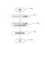
図1は、本実施形態に係る素子チップの製造方法を示すフローチャートである。Figure 1 is a flowchart showing the manufacturing method of the element chip according to this embodiment.
(1)準備工程(S1)
まず、ダイシングの対象となる半導体基板を準備する。 (1) Preparation process (S1)
First, a semiconductor substrate to be diced is prepared.
(半導体基板)
半導体基板は、複数の素子領域、素子領域を画定する分割領域、およびアライメントマークを備える第1主面と、第1主面の反対側の第2主面とを有する第1層を備える。第1層は、半導体層を含む。 (Semiconductor Substrate)
The semiconductor substrate includes a first layer having a first main surface including a plurality of element regions, division regions that define the element regions, and alignment marks, and a second main surface opposite to the first main surface. The first layer includes a semiconductor layer.
第1層は、さらに第1主面側に配線層および絶縁膜を備えてもよい。この場合、素子領域に対応する半導体基板は、例えば、配線層と半導体層とを備える。分割領域に対応する半導体基板は、例えば、絶縁膜と半導体層とを備える。絶縁膜は、TEG(Test Element Group)などの金属材料を含んでもよい。分割領域に対応する半導体基板を厚さ方向にエッチングすることにより、複数の素子チップが得られる。The first layer may further include a wiring layer and an insulating film on the first main surface side. In this case, the semiconductor substrate corresponding to the element region includes, for example, a wiring layer and a semiconductor layer. The semiconductor substrate corresponding to the division region includes, for example, an insulating film and a semiconductor layer. The insulating film may include a metal material such as TEG (Test Element Group). By etching the semiconductor substrate corresponding to the division region in the thickness direction, multiple element chips are obtained.
半導体基板の大きさは特に限定されず、例えば、最大径50mm以上、300mm以下程度である。半導体基板の形状も特に限定されず、例えば、円形、角形、六角形である。また、半導体基板には、オリエンテーションフラット(オリフラ)、ノッチなどの切欠きが設けられてもよい。The size of the semiconductor substrate is not particularly limited, and may be, for example, a maximum diameter of 50 mm or more and 300 mm or less. The shape of the semiconductor substrate is also not particularly limited, and may be, for example, a circle, a square, or a hexagon. The semiconductor substrate may also be provided with a cutout such as an orientation flat or a notch.
半導体層は、例えば、シリコン(Si)、ガリウム砒素(GaAs)、窒化ガリウム(GaN)、炭化ケイ素(SiC)などを含む。素子チップにおける半導体層の厚さは特に限定されず、例えば、20μm以上、1000μm以下であり、100μm以上、300μm以下であってもよい。The semiconductor layer includes, for example, silicon (Si), gallium arsenide (GaAs), gallium nitride (GaN), silicon carbide (SiC), etc. The thickness of the semiconductor layer in the element chip is not particularly limited and may be, for example, 20 μm or more and 1000 μm or less, or 100 μm or more and 300 μm or less.
配線層は、例えば、半導体回路、電子部品素子、MEMSなどを構成しており、絶縁膜、金属材料、樹脂層(例えば、ポリイミド)、レジスト層、電極パッド、バンプなどを備えてもよい。絶縁膜は、配線用の金属材料との積層体(多層配線層あるいは再配線層)として含まれてもよい。The wiring layer constitutes, for example, a semiconductor circuit, an electronic component element, a MEMS, etc., and may include an insulating film, a metal material, a resin layer (e.g., polyimide), a resist layer, an electrode pad, a bump, etc. The insulating film may be included as a laminate with a metal material for wiring (a multilayer wiring layer or a rewiring layer).
分割領域の形状は、直線状に限られず、所望の素子チップの形状に応じて設定されればよく、ジグザグ状であってもよいし、波線状であってもよい。なお、素子チップの形状としては、例えば、矩形、六角形などが挙げられる。The shape of the division region is not limited to a straight line, but may be zigzag or wavy as long as it is set according to the desired shape of the element chip. Examples of the shape of the element chip include a rectangle and a hexagon.
分割領域の幅は特に限定されず、半導体基板や素子チップの大きさなどに応じて、適宜設定すればよい。分割領域の幅は、例えば、10μm以上、300μm以下である。複数の分割領域の幅は、同じであってもよいし、異なっていてもよい。分割領域は、通常、半導体基板に複数本配置されている。隣接する分割領域同士のピッチも特に限定されず、半導体基板や素子チップの大きさなどに応じて、適宜設定すればよい。The width of the divided regions is not particularly limited, and may be set appropriately depending on the size of the semiconductor substrate and the element chip. The width of the divided regions is, for example, 10 μm or more and 300 μm or less. The widths of the multiple divided regions may be the same or different. Multiple divided regions are usually arranged on the semiconductor substrate. The pitch between adjacent divided regions is also not particularly limited, and may be set appropriately depending on the size of the semiconductor substrate and the element chip.
アライメントマークは、半導体基板の位置決めのために第1主面の表面に配置されている。アライメントマークは特に限定されず、分割領域と素子領域との境界を示すマーク(例えば、シールあるいはシールリングと称される金属パターン、スクライブラインと称される絶縁材料によるパターンなど)であってもよく、位置決めのために特別に設けられたマークであってもよい。アライメントマークは、通常、画像認識により半導体層および配線層とは区別可能である。アライメントマークの形状は特に限定されない。アライメントマークの形状は、複数の直線の組合せ(例えば、平行線、格子など)であってもよく、十字形、円形、矩形などであってもよい。境界線以外のアライメントマークは、例えば、分割領域であって半導体基板の外縁部分に配置される。アライメントマークは、必要に応じて、素子領域に配置されてもよい。The alignment mark is arranged on the surface of the first main surface for positioning the semiconductor substrate. The alignment mark is not particularly limited, and may be a mark indicating the boundary between the division region and the element region (for example, a metal pattern called a seal or seal ring, a pattern made of an insulating material called a scribe line, etc.), or may be a mark specially provided for positioning. The alignment mark can usually be distinguished from the semiconductor layer and the wiring layer by image recognition. The shape of the alignment mark is not particularly limited. The shape of the alignment mark may be a combination of multiple straight lines (for example, parallel lines, a grid, etc.), or may be a cross, a circle, a rectangle, etc. Alignment marks other than the boundary line are arranged, for example, in the division region, which is the outer edge portion of the semiconductor substrate. The alignment mark may be arranged in the element region as necessary.
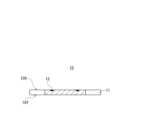
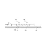
図2Aは、第1主面側から見た半導体基板を模式的に示す上面図である。図2Bは、図2Aに示される半導体基板のX-X線における断面図である。Figure 2A is a top view showing a schematic diagram of a semiconductor substrate viewed from the first main surface side. Figure 2B is a cross-sectional view of the semiconductor substrate shown in Figure 2A taken along line X-X.
半導体基板10は、複数の素子領域101、素子領域101を画定する分割領域102、およびアライメントマーク15を備える第1主面10Xと、第1主面10Xの反対側の第2主面10Yとを有する第1層を備える。第1層は、半導体層11を含む。第1主面10Xの外縁には、十字形のアライメントマーク15が4箇所配置されている。半導体基板10は、1箇所のノッチ10aを備える。The
(2)貼着工程(S2)
準備工程の後、ダイシング工程よりも前に(この例では、研磨工程の前に)、半導体基板の第1主面を保持シートに貼着してもよい。これにより、半導体基板のハンドリング性が向上する。 (2) Pasting process (S2)
After the preparation step and before the dicing step (before the polishing step in this example), the first main surface of the semiconductor substrate may be attached to a holding sheet, which improves the handleability of the semiconductor substrate.
(保持シート)
ハンドリング性がより向上する点で、保持シートはフレームに固定されてもよい。半導体基板は、例えば、フレームとフレームに固定された保持シートとを備える搬送キャリアに保持された状態で各工程に供されてもよい。 (Retaining sheet)
In order to improve handling, the holding sheet may be fixed to a frame. The semiconductor substrate may be subjected to each process while being held by, for example, a transport carrier including a frame and a holding sheet fixed to the frame.
フレームは、半導体基板の全体と同じかそれ以上の面積の開口を有する枠体であり、所定の幅および略一定の薄い厚さを有する。フレームは、保持シートおよび半導体基板を保持した状態で搬送できる程度の剛性を有する。フレームの開口の形状は特に限定されないが、例えば、円形や、矩形、六角形など多角形であってもよい。フレームの材質としては、例えば、アルミニウム、ステンレス鋼などの金属や、樹脂などが挙げられる。The frame is a frame body having an opening with an area equal to or greater than the entire semiconductor substrate, and has a predetermined width and a generally constant thin thickness. The frame has a degree of rigidity that allows it to be transported while holding the holding sheet and semiconductor substrate. The shape of the opening of the frame is not particularly limited, but may be, for example, a circle or a polygon such as a rectangle or hexagon. Examples of materials for the frame include metals such as aluminum and stainless steel, and resins.
保持シートの材質は特に限定されない。中でも、半導体基板が貼着されやすい点で、保持シートは、粘着層と柔軟性のある非粘着層とを含むことが好ましい。The material of the holding sheet is not particularly limited. In particular, it is preferable that the holding sheet includes an adhesive layer and a flexible non-adhesive layer, since this makes it easy to attach the semiconductor substrate.
非粘着層の材質は特に限定されず、例えば、ポリエチレンおよびポリプロピレンなどのポリオレフィン、ポリ塩化ビニル、ポリエチレンテレフタレートなどのポリエステルなどの熱可塑性樹脂が挙げられる。樹脂フィルムには、伸縮性を付加するためのゴム成分(例えば、エチレン-プロピレンゴム(EPM)、エチレン-プロピレン-ジエンゴム(EPDM)など)、可塑剤、軟化剤、酸化防止剤、導電性材料などの各種添加剤が配合されていてもよい。また、上記熱可塑性樹脂は、アクリル基などの光重合反応を示す官能基を有してもよい。非粘着層の厚さは特に限定されず、例えば、50μm以上、300μm以下であり、好ましくは50μm以上、150μm以下である。The material of the non-adhesive layer is not particularly limited, and examples thereof include thermoplastic resins such as polyolefins such as polyethylene and polypropylene, and polyesters such as polyvinyl chloride and polyethylene terephthalate. The resin film may contain various additives such as rubber components (e.g., ethylene-propylene rubber (EPM), ethylene-propylene-diene rubber (EPDM)) to impart elasticity, plasticizers, softeners, antioxidants, and conductive materials. The thermoplastic resin may also have functional groups that exhibit photopolymerization reactions, such as acrylic groups. The thickness of the non-adhesive layer is not particularly limited, and is, for example, 50 μm or more and 300 μm or less, and preferably 50 μm or more and 150 μm or less.
粘着層を備える面(粘着面)の外周縁は、フレームの一方の面に貼着しており、フレームの開口を覆っている。粘着面のうちフレームの開口から露出した部分に、半導体基板の一方の主面(第1主面)が貼着されることにより、半導体基板は保持シートに保持される。半導体基板は、ダイアタッチフィルム(DAF)を介して、保持シートに保持されてもよい。The outer edge of the surface having the adhesive layer (adhesive surface) is attached to one surface of the frame, covering the opening of the frame. One main surface (first main surface) of the semiconductor substrate is attached to the portion of the adhesive surface exposed from the opening of the frame, thereby holding the semiconductor substrate on the holding sheet. The semiconductor substrate may be held on the holding sheet via a die attach film (DAF).
粘着層は、紫外線(UV)の照射によって粘着力が減少する粘着成分からなることが好ましい。これにより、ダイシング後に素子チップをピックアップする際、UV照射を行うことで、素子チップが粘着層から容易に剥離されて、ピックアップしやすくなる。例えば、粘着層は、非粘着層の片面に、UV硬化型アクリル粘着剤を5μm以上、100μm以下(好ましくは5μm以上、15μm以下)の厚さに塗布することにより得られる。The adhesive layer is preferably made of an adhesive component whose adhesive strength decreases when irradiated with ultraviolet (UV) light. As a result, when picking up the element chip after dicing, UV irradiation allows the element chip to be easily peeled off from the adhesive layer, making it easier to pick up. For example, the adhesive layer can be obtained by applying a UV-curable acrylic adhesive to one side of the non-adhesive layer to a thickness of 5 μm or more and 100 μm or less (preferably 5 μm or more and 15 μm or less).
図3は、搬送キャリアとこれに保持された半導体基板とを模式的に示す上面図である。図4は、本実施形態に係る貼着工程後の半導体基板の、図2AのX-X線における断面図である。搬送キャリア20は、フレーム21とフレーム21に固定された保持シート22とを備える。フレーム21には、位置決めのためのノッチ21aやコーナーカット21bが設けられてもよい。保持シート22の粘着面22Xの外周縁は、フレーム21の一方の面に貼着し、粘着面22Xのうちフレーム21の開口から露出した部分に、半導体基板10の一方の主面が貼着される。プラズマ処理の際、保持シート22は、プラズマ処理装置内に設置されるステージと、粘着面22Xとは反対側の非粘着面22Yとが接するように、ステージに載置される。Figure 3 is a top view showing a schematic diagram of a transport carrier and a semiconductor substrate held thereon. Figure 4 is a cross-sectional view of the semiconductor substrate after the bonding process according to this embodiment, taken along line X-X in Figure 2A. The
(3)研磨工程(S3)
被覆工程よりも前に、半導体基板の第2主面を研磨してもよい。これにより、第2主面の平滑性が向上する。また、この研磨工程では、半導体基板を所望の厚さまで薄くしてもよい。 (3) Polishing process (S3)
Prior to the covering step, the second main surface of the semiconductor substrate may be polished to improve the smoothness of the second main surface, and the polishing step may thin the semiconductor substrate to a desired thickness.
(4)被覆工程(S4)
第2主面におけるアライメントマークに対応する第1領域をレジスト膜で被覆する。 (4) Covering process (S4)
A first area on the second main surface corresponding to the alignment mark is covered with a resist film.
レジスト膜は、レジスト材料を含む。レジスト材料は、液状のレジスト溶液に含まれていてもよいし、ドライフィルムレジストでもよい。レジスト材料は、例えばフォトレジストであってもよい。フォトレジストは、例えば、レジスト樹脂、感光剤、添加剤などを含む。レジスト樹脂は、特に限定されないが、例えばノボラック型樹脂(フェノールノボラック樹脂など)が使用される。感光剤としては、例えば光照射により酸性度の強い有機酸を生成する酸発生剤を用いることができる。レジスト膜は、ポジ型でもよく、ネガ型でもよいが、パターニングされたレジスト膜の断面形状の露光量による調整が容易であることから、ネガ型レジストが好ましい。レジスト樹脂は、水溶性樹脂であってもよい。レジスト膜の厚さは特に限定されないが、後述する第1露出工程(S6)における金属膜の除去(リフトオフ)を容易とするため、後述する金属膜形成工程(S5)で形成される金属膜の膜厚よりも厚い方が好ましい。The resist film includes a resist material. The resist material may be contained in a liquid resist solution or may be a dry film resist. The resist material may be, for example, a photoresist. The photoresist includes, for example, a resist resin, a photosensitizer, an additive, and the like. The resist resin is not particularly limited, but for example, a novolac resin (such as a phenol novolac resin) is used. As the photosensitizer, for example, an acid generator that generates an organic acid with high acidity upon irradiation with light can be used. The resist film may be a positive type or a negative type, but a negative type resist is preferred because it is easy to adjust the cross-sectional shape of the patterned resist film by the amount of exposure. The resist resin may be a water-soluble resin. The thickness of the resist film is not particularly limited, but it is preferable that the thickness is thicker than the thickness of the metal film formed in the metal film formation process (S5) described later in order to facilitate removal (lift-off) of the metal film in the first exposure process (S6) described later.
レジスト膜の形成方法は、特に限定されないが、レジスト溶液を塗布して形成してもよく、ドライフィルムレジストを貼り合わせ機を用いて貼り付けることにより形成してもよい。レジスト溶液は、例えば、レジスト材料と溶媒を含む。溶媒は、特に限定されないが、例えば、メチルエチルケトン、プロピレングリコールモノメチルエーテルアセテートなどを用い得る。レジスト溶液を第2主面に塗布して塗膜を形成し、塗膜を乾燥させることでレジスト膜が形成される。乾燥のために塗膜を加熱する温度は、50℃以上でもよく、60℃以上でもよく、90℃以上でもよい。The method for forming the resist film is not particularly limited, but may be formed by applying a resist solution, or may be formed by pasting a dry film resist using a laminating machine. The resist solution contains, for example, a resist material and a solvent. The solvent is not particularly limited, but may be, for example, methyl ethyl ketone, propylene glycol monomethyl ether acetate, or the like. The resist film is formed by applying the resist solution to the second main surface to form a coating film, and drying the coating film. The temperature to which the coating film is heated for drying may be 50°C or higher, 60°C or higher, or 90°C or higher.
塗膜を第2主面に形成する(レジスト溶液を第2主面に塗布する)手法は、レジスト溶液が第2主面上に均一に塗布される手法であればよく、例えば、回転塗布やスプレー塗布、スリットコートなどの手法でもよい。回転塗布は、スピンコーティング塗布装置を用いて行われる。スプレー塗布は、スプレー塗布装置を用いて行われる。スリットコートは、スリットコータを用いて行われる。The method for forming a coating film on the second main surface (applying the resist solution to the second main surface) may be any method that allows the resist solution to be applied uniformly onto the second main surface, and may be, for example, spin coating, spray coating, slit coating, or other methods. Spin coating is performed using a spin coating application device. Spray coating is performed using a spray application device. Slit coating is performed using a slit coater.
次に、レジスト膜をパターニングして、第1領域を選択的にレジスト膜で被覆する。パターニングは、第1領域の配置に対応するパターンでレジスト膜に光を照射する露光工程と、第1領域以外を覆うレジスト膜を現像液で除去する現像工程とを有する。パターニングは、さらに、残存する現像液を純水などで洗浄する洗浄工程を有してもよい。露光工程は、例えばUV光をレジスト膜に照射することにより、レジスト膜の現像液に対する溶解性を変化させる工程である。現像工程は、レジスト膜の特性に適合した現像液および現像方式(ディップ現像またはスプレー現像)を用いて行えばよい。なお、露光条件や現像条件を調整することにより、パターニングされたレジスト膜の断面形状を逆テーパ状にすることが好ましい。レジスト膜の断面形状を逆テーパ状にすることにより、後述する金属膜形成工程において、パターニングされたレジスト膜の側面に金属膜が形成されにくくなるため、後述する第1露出工程において、第1領域に対応する半導体層を露出させやすくすることができる。Next, the resist film is patterned to selectively cover the first region with the resist film. The patterning includes an exposure process in which the resist film is irradiated with light in a pattern corresponding to the arrangement of the first region, and a development process in which the resist film covering the region other than the first region is removed with a developer. The patterning may further include a washing process in which the remaining developer is washed with pure water or the like. The exposure process is a process in which the resist film is irradiated with UV light, for example, to change the solubility of the resist film in the developer. The development process may be performed using a developer and a development method (dip development or spray development) that are suitable for the characteristics of the resist film. It is preferable to make the cross-sectional shape of the patterned resist film in an inverse tapered shape by adjusting the exposure conditions and development conditions. By making the cross-sectional shape of the resist film in an inverse tapered shape, it becomes difficult to form a metal film on the side of the patterned resist film in the metal film formation process described later, so that it is possible to easily expose the semiconductor layer corresponding to the first region in the first exposure process described later.
(第1領域)
第1領域は、例えば、半導体基板に設けられたオリフラやノッチなどの切欠きの位置、あるいは、フレームに設けられたコーナーカットやノッチなどの切欠きの位置から、設計図などの設計情報を参照して決定される。設計情報には、各切欠きとアライメントマークとの位置関係が示されている。切欠きの位置から決定されたアライメントマークに対応する第2主面の一部が、第1領域である。換言すると、アライメントマークの少なくとも一部と第1領域の少なくとも一部とは対向しており、第2主面の法線方向から見たとき、アライメントマークの少なくとも一部は第1領域と重複する。 (First region)
The first region is determined, for example, from the position of a cutout such as an orientation flat or a notch provided on a semiconductor substrate, or the position of a cutout such as a corner cut or a notch provided on a frame, with reference to design information such as a design drawing. The design information indicates the positional relationship between each cutout and an alignment mark. A part of the second main surface corresponding to the alignment mark determined from the position of the cutout is the first region. In other words, at least a part of the alignment mark and at least a part of the first region face each other, and at least a part of the alignment mark overlaps with the first region when viewed from the normal direction of the second main surface.
上記のように設計情報を参照して決定されるアライメントマークの位置は、基板の寸法ばらつきやアライメントマーク形成位置のばらつき等により、実際のアライメントマークの位置とずれている場合がある。しかし、例えば、数百μm程度の位置ずれは許容される。ここでは、第2主面において、アライメントマークに対応する比較的広い領域を第1領域として決定すればよい。The position of the alignment mark determined by referring to the design information as described above may deviate from the actual position of the alignment mark due to variations in the dimensions of the substrate and variations in the position of the alignment mark formation. However, a positional deviation of, for example, several hundred μm is permissible. Here, a relatively wide area on the second main surface that corresponds to the alignment mark may be determined as the first area.
アライメントマークが境界線である場合、第1領域は、少なくとも2本の境界線の一部(例えば、格子状の境界線の交点、隣接する2本の平行線の一部)を含む。このような第1領域は、例えば、半導体基板の外縁に沿う円弧あるいはリングである。境界線以外のアライメントマークの場合、第2主面の法線方向から見たとき、アライメントマークの全体が第1領域と重複する。境界線以外のアライメントマークを囲む最小の円を描いたとき、当該円の直径の5~10倍の程度の直径(あるいは、長辺長さ)を有し、当該円と重複する円形または矩形の部分を第1領域と決定すればよい。When the alignment mark is a boundary line, the first region includes at least parts of two boundary lines (e.g., an intersection of a grid-like boundary line, or parts of two adjacent parallel lines). Such a first region is, for example, an arc or ring along the outer edge of the semiconductor substrate. When an alignment mark is not a boundary line, the entire alignment mark overlaps with the first region when viewed from the normal direction of the second main surface. When the smallest circle that surrounds the alignment mark other than a boundary line is drawn, the circular or rectangular portion that has a diameter (or long side length) of about 5 to 10 times the diameter of the circle and overlaps with the circle can be determined as the first region.
算出工程で使用されるカメラの視野に、金属膜形成工程で形成される金属膜が入り込まないように、第1領域を決定することが好ましい。金属膜をアライメントマークと誤認することを避けるためである。例えば、上記最小の円の直径が100μmであり、カメラの視野が300μm四方である場合、第1領域の直径(あるいは、長辺長さ)は500μm程度であればよい。It is preferable to determine the first region so that the metal film formed in the metal film formation process does not enter the field of view of the camera used in the calculation process. This is to avoid mistaking the metal film for an alignment mark. For example, if the diameter of the smallest circle is 100 μm and the field of view of the camera is 300 μm square, the diameter (or the length of the long side) of the first region should be approximately 500 μm.
図5は、本実施形態に係る被覆工程後の半導体基板の、図2AのX-X線における断面図である。半導体基板10の第2主面10Yにおける第1領域R1に、レジスト膜50が形成されている。レジスト膜50は、表面側(第2主面10Yから遠い方)から裏面側(第2主面10Yに近い方)に向かって幅狭になっている。このような逆テーパ形状により、この後の金属膜形成工程において、第2主面10Y上に形成される金属膜30と、レジスト膜50上に形成される金属膜30とが互いに分離しやすくなる。Figure 5 is a cross-sectional view of the semiconductor substrate after the coating process according to this embodiment, taken along line X-X in Figure 2A. A resist
(5)金属膜形成工程(S5)
被覆工程の後、半導体基板の第2主面上に金属膜を形成する。 (5) Metal film forming step (S5)
After the covering step, a metal film is formed on the second main surface of the semiconductor substrate.
金属膜は、例えば、厚さ方向に電流を流したり、放熱性を高めたりするために形成される。金属膜は、半導体層に隣接して配置されるが、両者の間に接着剤層などが介在してもよい。金属膜の材料は、例えば、銀、銅、アルミニウム、アルミニウム合金、タングステン、ニッケル、金、白金、チタンなどである。金属膜は、例えば、蒸着法、スパッタ法、メッキ法などにより形成される。金属膜は単層であってもよく、2層以上であってもよい。金属膜は、例えば、半導体層にチタンとニッケルと金とを順番に積層したもの(Au/Ni/Ti)であってもよく、半導体層にチタンとニッケルと銀とを順番に積層したもの(Ag/Ni/Ti)であってもよく、半導体層にチタンとニッケルとアルミニウム合金とを順番に積層したもの(Al合金/Ni/Ti)であってもよい。The metal film is formed, for example, to pass a current in the thickness direction or to improve heat dissipation. The metal film is disposed adjacent to the semiconductor layer, but an adhesive layer or the like may be interposed between the two. The material of the metal film is, for example, silver, copper, aluminum, aluminum alloy, tungsten, nickel, gold, platinum, titanium, etc. The metal film is formed, for example, by a vapor deposition method, a sputtering method, a plating method, etc. The metal film may be a single layer, or may be two or more layers. The metal film may be, for example, a semiconductor layer in which titanium, nickel, and gold are laminated in order (Au/Ni/Ti), a semiconductor layer in which titanium, nickel, and silver are laminated in order (Ag/Ni/Ti), or a semiconductor layer in which titanium, nickel, and aluminum alloy are laminated in order (Al alloy/Ni/Ti).
金属膜の厚さ(合計の厚さ)は特に限定されず、素子チップの用途などにより適宜設定される。金属膜の厚さは、例えば、50nm以上、100μm以下である。金属膜がAu/Ni/Tiの積層体である場合、例えば、Auの膜厚は50nm以上、200nm以下であり、Niの膜厚は200nm以上、400nm以下であり、Tiの膜厚は100nm以上、300nm以下である。金属膜がAg/Ni/Tiの積層体である場合、例えば、Agの膜厚は200nm以上、30μm以下であり、Niの膜厚は200nm以上、400nm以下であり、Tiの膜厚は100nm以上、300nm以下である。金属膜がAl合金/Ni/Tiの積層体である場合、例えば、Al合金の膜厚は200nm以上、30μm以下であり、Niの膜厚は200nm以上、400nm以下であり、Tiの膜厚は100nm以上、300nm以下である。The thickness (total thickness) of the metal film is not particularly limited and is appropriately set depending on the application of the element chip. The thickness of the metal film is, for example, 50 nm or more and 100 μm or less. When the metal film is a laminate of Au/Ni/Ti, for example, the thickness of Au is 50 nm or more and 200 nm or less, the thickness of Ni is 200 nm or more and 400 nm or less, and the thickness of Ti is 100 nm or more and 300 nm or less. When the metal film is a laminate of Ag/Ni/Ti, for example, the thickness of Ag is 200 nm or more and 30 μm or less, the thickness of Ni is 200 nm or more and 400 nm or less, and the thickness of Ti is 100 nm or more and 300 nm or less. When the metal film is a laminate of Al alloy/Ni/Ti, for example, the thickness of the Al alloy is 200 nm or more and 30 μm or less, the thickness of the Ni is 200 nm or more and 400 nm or less, and the thickness of the Ti is 100 nm or more and 300 nm or less.
図6は、本実施形態に係る金属膜形成工程後の半導体基板の、図2AのX-X線における断面図である。半導体基板10の第2主面10Yにおける第1領域R1を除く領域に、金属膜30が形成されている。また、レジスト膜50上にも金属膜30が形成されている。第2主面10Y上の金属膜30と、レジスト膜50上の金属膜30とは、互いに分離している。ただし、両者の金属膜30は、互いにつながっていてもよい。Figure 6 is a cross-sectional view of the semiconductor substrate after the metal film formation process according to this embodiment, taken along line X-X in Figure 2A. A
(6)第1露出工程(S6)
金属膜形成工程の後、レジスト膜とその上の金属膜を除去(リフトオフ)し、第1領域に対応する半導体層を露出させる。 (6) First exposure step (S6)
After the metal film forming step, the resist film and the metal film thereon are removed (lifted off) to expose the semiconductor layer corresponding to the first region.
第1露出工程では、レジスト膜を溶解させる溶液(現像液)を半導体基板に接触させることにより、レジスト膜とその上の金属膜を除去してもよい。レジスト膜を溶解させる溶液の種類は特に限定されない。In the first exposure step, the resist film and the metal film thereon may be removed by contacting the semiconductor substrate with a solution (developer) that dissolves the resist film. There are no particular limitations on the type of solution that dissolves the resist film.
図7Aは、本実施形態に係る第1露出工程後の半導体基板の、図2AのX-X線における断面図である。図7Bは、本実施形態に係る第1露出工程後の半導体基板を模式的に示す上面図である。半導体基板10の第1主面10X上に配置された4箇所のアライメントマーク15の全体がそれぞれ露出するように、4箇所の第1領域R1におけるレジスト膜50と金属膜30が除去されている。第1領域R1は、アライメントマーク15を取り囲む円形である。図7Bでは、便宜的に金属膜30にハッチングを入れて示している。Figure 7A is a cross-sectional view of the semiconductor substrate after the first exposure step according to this embodiment, taken along line X-X in Figure 2A. Figure 7B is a top view that shows a schematic diagram of the semiconductor substrate after the first exposure step according to this embodiment. The resist
(7)保護膜形成工程(S7)
第2露出工程よりも前に(この例では、算出工程の前に)、金属膜の表面を被覆する保護膜を形成する。保護膜は、ダイシング工程において、素子領域に対応する金属膜をダイシング工程で用いるプラズマやダイシング工程で生成するデブリから保護する。第2領域に対応する保護膜は、第2露出工程において金属膜と共に除去される。 (7) Protective film formation step (S7)
Prior to the second exposure step (in this example, prior to the calculation step), a protective film is formed to cover the surface of the metal film. The protective film protects the metal film corresponding to the element region from plasma used in the dicing step and debris generated in the dicing step in the dicing step. The protective film corresponding to the second region is removed together with the metal film in the second exposure step.
(保護膜)
保護膜は、例えば、ポリイミドなどの熱硬化性樹脂、フォトレジストなどのレジスト材料、あるいは、アクリル樹脂などの水溶性樹脂を含む。保護膜は、例えば、保護膜の原料液を、回転塗布やスプレー塗布などの方法を用いて金属膜の表面に塗布することにより形成される。中でも、水洗による除去が可能な点で水溶性樹脂が好ましい。水溶性樹脂としては、例えば、ポリビニルアルコール、ポリアクリルアミド、ポリビニルピロリドン、2-アクリルアミド-2-メチルプロパンスルホン酸、ポリアクリル酸ナトリウム、ポリスチレンスルホン酸ナトリウム、ポリスチレンスルホン酸リチウム、ジアリルジメチルアンモニウムクロライドなどを用い得る。 (Protective Film)
The protective film includes, for example, a thermosetting resin such as polyimide, a resist material such as a photoresist, or a water-soluble resin such as an acrylic resin. The protective film is formed, for example, by applying a raw material liquid of the protective film to the surface of the metal film using a method such as spin coating or spray coating. Among them, a water-soluble resin is preferable because it can be removed by washing with water. Examples of the water-soluble resin that can be used include polyvinyl alcohol, polyacrylamide, polyvinylpyrrolidone, 2-acrylamido-2-methylpropanesulfonic acid, sodium polyacrylate, sodium polystyrenesulfonate, lithium polystyrenesulfonate, and diallyldimethylammonium chloride.
保護膜の厚さは特に限定されないが、プラズマダイシング工程において完全には除去されない程度であることが好ましい。保護膜の厚さは、例えば、プラズマダイシング工程において保護膜がエッチングされる量(厚さ)を算出し、このエッチング量以上になるように設定される。The thickness of the protective film is not particularly limited, but it is preferable that the thickness is such that it is not completely removed in the plasma dicing process. For example, the thickness of the protective film is calculated by calculating the amount (thickness) of the protective film that is etched in the plasma dicing process, and set to be equal to or greater than this amount of etching.
保護膜は、半導体層を透過する電磁波を透過させる。このため、半導体層が露出した第1領域に保護膜が形成されても、算出工程で使用されるカメラによるアライメントマークの撮像は、当該保護膜によって妨げられない。The protective film allows electromagnetic waves to pass through the semiconductor layer. Therefore, even if a protective film is formed on the first region where the semiconductor layer is exposed, the protective film does not prevent the camera used in the calculation process from capturing an image of the alignment mark.
図8は、本実施形態に係る保護膜形成工程後の半導体基板の、図2AのX-X線における断面図である。保護膜40は、半導体基板10の金属膜30を覆うように形成される。Figure 8 is a cross-sectional view of the semiconductor substrate after the protective film formation process according to this embodiment, taken along line X-X in Figure 2A. The
(8)算出工程(S8)
半導体基板を金属膜の表面側から半導体層を透過する電磁波を感知するカメラにより撮像して、第1領域に対応する半導体層を通してアライメントマークの位置および形状などを検出する。検出されたアライメントマークに関するデータに基づき、金属膜の表面における分割領域に対応する第2領域が算出される。 (8) Calculation step (S8)
The semiconductor substrate is imaged from the surface side of the metal film by a camera that senses electromagnetic waves transmitted through the semiconductor layer, and the position and shape of the alignment mark are detected through the semiconductor layer corresponding to the first region. Based on data related to the detected alignment mark, a second region corresponding to the divided region on the surface of the metal film is calculated.
(カメラ)
カメラは、半導体層を透過する電磁波を感知することができる。これにより、金属膜の表面側から第1領域に対応する半導体層を通してアライメントマークを撮像することができる。なお、半導体層を透過する電磁波は、例えば、金属膜の表面側に配置され、ピーク波長が1000nm以上である近赤外ハロゲンランプにより発生させてもよい。 (camera)
The camera can sense the electromagnetic waves transmitted through the semiconductor layer. This allows the alignment mark to be imaged from the front side of the metal film through the semiconductor layer corresponding to the first region. The electromagnetic waves transmitted through the semiconductor layer may be generated by, for example, a near-infrared halogen lamp disposed on the front side of the metal film and having a peak wavelength of 1000 nm or more.
カメラは、例えば、近赤外領域(750nm以上、1200nm以下の波長帯)の電磁波を感知できる赤外線カメラを用いることも可能であるが、より長い波長域に感度を持つ赤外線カメラの方が好ましい。赤外線カメラは、後述するレーザ光照射装置の撮像部を構成する。撮像部は、赤外線カメラ以外のカメラ(例えば、可視光を感知するカメラなど)を備えてもよい。撮像部は、複数の赤外線カメラを備えてもよい。赤外線カメラの視野は特に限定されないが、精度向上の観点から300μm四方以上であってもよい。The camera may be, for example, an infrared camera capable of detecting electromagnetic waves in the near-infrared region (wavelength band of 750 nm or more and 1200 nm or less), but an infrared camera with sensitivity to longer wavelengths is preferable. The infrared camera constitutes the imaging section of the laser light irradiation device described below. The imaging section may include a camera other than an infrared camera (for example, a camera that detects visible light). The imaging section may include multiple infrared cameras. The field of view of the infrared camera is not particularly limited, but may be 300 μm square or more from the viewpoint of improving accuracy.
(レーザ光照射装置)
レーザ光照射装置は、例えば、半導体基板の搬出入を行うアーム、半導体基板を載置するステージ、レーザ光を照射する照射ヘッド、ステージを駆動させる駆動部、分割領域、第1領域および/またはアライメントマークに関するデータが入力される入力部、ステージに載置された半導体基板を撮像する撮像部、撮像された半導体基板の形状などを検出する画像処理部、画像処理部で検出された半導体基板の形状などと入力されたデータとに基づいて、半導体基板の位置、第1領域および/または第2領域を決定する演算部、および、これらを制御する制御部を備える。 (Laser light irradiation device)
The laser light irradiation device includes, for example, an arm for loading and unloading the semiconductor substrate, a stage for placing the semiconductor substrate, an irradiation head for irradiating the laser light, a drive unit for driving the stage, an input unit for inputting data relating to the divided region, the first region and/or the alignment mark, an imaging unit for imaging the semiconductor substrate placed on the stage, an image processing unit for detecting the shape of the imaged semiconductor substrate, etc., a calculation unit for determining the position of the semiconductor substrate, the first region and/or the second region based on the shape of the semiconductor substrate detected by the image processing unit and the input data, and a control unit for controlling these.
入力部は、例えばタッチパネルを備える。入力部には、例えばオペレータによって、上記各種データが入力される。制御部、画像処理部、および演算部は、例えばコンピュータを備える。撮像部は、カメラを備える。駆動部は、例えば、ボールネジとリニアガイド機構を備える。ボールネジが回転することにより、ステージは、照射ヘッドおよびカメラの下方で並進移動および/または垂直移動する。The input unit includes, for example, a touch panel. The above-mentioned various data are input to the input unit, for example, by an operator. The control unit, image processing unit, and calculation unit include, for example, a computer. The imaging unit includes, for example, a camera. The drive unit includes, for example, a ball screw and a linear guide mechanism. As the ball screw rotates, the stage moves translationally and/or vertically below the irradiation head and the camera.
(第2領域)
第2領域は、検出されたアライメントマークの位置と入力部のデータとから算出される。第2領域は、分割領域に対応する金属膜の表面の一部である。換言すると、分割領域の少なくとも一部と第2領域の少なくとも一部とは対向しており、金属膜の表面の法線方向から見たとき、分割領域の少なくとも一部は第2領域と重複する。好ましくは、分割領域全体が第2領域と重複する。 (Second Area)
The second region is calculated from the position of the detected alignment mark and the data of the input unit. The second region is a part of the surface of the metal film corresponding to the divided region. In other words, at least a part of the divided region and at least a part of the second region face each other, and when viewed from the normal direction of the surface of the metal film, at least a part of the divided region overlaps with the second region. Preferably, the entire divided region overlaps with the second region.
図9は、本実施形態に係るレーザ光照射装置の算出工程における動作を示すフローチャートである。Figure 9 is a flowchart showing the operation of the calculation process of the laser light irradiation device according to this embodiment.
保護膜形成工程が終了すると、レーザ光照射装置の算出工程における動作が開始される(T10)。駆動部はステージを駆動して、第1領域を赤外線カメラの下方に移動させる。撮像部は、金属膜の表面側から、赤外線カメラにより第1領域に対応する半導体層を通してアライメントマークを撮像する(T11)。画像処理部は撮像された画像を処理して、アライメントマークの位置および形状などを検出する(T12)。演算部は、検出されたアライメントマークおよび入力された分割領域に関するデータから、金属膜の表面における分割領域の位置を算出する(T13)。これにより、金属膜の表面における分割領域に対応する第2領域が決定される。その後、レーザ光照射装置の算出工程における動作は終了する(T14)。When the protective film formation process is completed, the operation of the calculation process of the laser light irradiation device is started (T10). The driving unit drives the stage to move the first region below the infrared camera. The imaging unit images the alignment mark from the surface side of the metal film through the semiconductor layer corresponding to the first region using the infrared camera (T11). The image processing unit processes the captured image to detect the position and shape of the alignment mark (T12). The calculation unit calculates the position of the divided region on the surface of the metal film from the detected alignment mark and the input data related to the divided region (T13). This determines the second region corresponding to the divided region on the surface of the metal film. Thereafter, the operation of the calculation process of the laser light irradiation device is completed (T14).
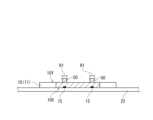
図10は、本実施形態の係る算出工程中の半導体基板の、図2AのX-X線における断面図である。赤外線カメラ300により第1領域R1に対応する半導体層11を通してアライメントマーク15が撮像される。撮像された画像は画像処理されて、アライメントマーク15の形状などが検出される。この検出されたアライメントマーク15の形状などから、分割領域の位置が算出される。Figure 10 is a cross-sectional view of the semiconductor substrate during the calculation process of this embodiment, taken along line X-X in Figure 2A. An
(9)第2露出工程(S9)
金属膜の表面側から第2領域に第1のレーザ光を照射して、第2領域に対応する保護膜および金属膜を除去する。これにより、第2領域に対応する半導体層が露出する。 (9) Second exposure step (S9)
The second region is irradiated with a first laser beam from the front surface side of the metal film to remove the protective film and the metal film corresponding to the second region, thereby exposing the semiconductor layer corresponding to the second region.
駆動部はステージを駆動して、半導体基板の端部を照射ヘッドの下方に移動させる。半導体基板が所定の位置に配置されると、照射部は第2領域への第1のレーザ光の照射を開始する。第1のレーザ光が照射された状態で、駆動部はさらに、第2領域の大きさおよび形状などに基づいてステージを平面方向に移動させる。これにより、第2領域に対応する保護膜と金属膜が除去される。The drive unit drives the stage to move the edge of the semiconductor substrate below the irradiation head. When the semiconductor substrate is positioned at a predetermined position, the irradiation unit starts irradiating the second region with the first laser light. While the first laser light is being irradiated, the drive unit further moves the stage in a planar direction based on the size and shape of the second region. This removes the protective film and metal film corresponding to the second region.
(第1のレーザ光)
第1のレーザ光は、金属膜に吸収される一方、半導体層を透過することが好ましい。その場合、第1のレーザ光の照射によって金属膜は除去されるものの、金属膜の下にある半導体層の表面の荒れや内部の結晶の乱れは抑制される。 (First laser light)
It is preferable that the first laser light is absorbed by the metal film and transmitted through the semiconductor layer, in which case the metal film is removed by irradiation with the first laser light, but roughness of the surface of the semiconductor layer below the metal film and disorder of the crystals inside the semiconductor layer are suppressed.
第1のレーザ光は、半導体層の損傷抑制の観点から、半導体層を構成する半導体に吸収され難い波長を有することが好ましい。例えば、半導体層がシリコンである場合、第1のレーザ光は、1100nm以上、6μm以下の波長を有することが好ましく、一酸化炭素レーザなどが例として挙げられる。第1のレーザ光の波長は、この波長域に限るものではなく、集光性が高いという利点を備える、より短い波長域であってもよい。具体的には、第1のレーザ光は、850nm以上、1100nm以下の波長を有してもよく、190nm以上、450nm以下の波長を有してもよい。より具体的には、第1のレーザ光の波長は、近赤外領域の980nm、1064nm、または1030nmであってもよいし、紫外領域の355nm、305nm、308nm、または266nmであってもよい。From the viewpoint of suppressing damage to the semiconductor layer, it is preferable that the first laser light has a wavelength that is not easily absorbed by the semiconductor that constitutes the semiconductor layer. For example, when the semiconductor layer is silicon, the first laser light preferably has a wavelength of 1100 nm or more and 6 μm or less, and an example thereof is a carbon monoxide laser. The wavelength of the first laser light is not limited to this wavelength range, and may be a shorter wavelength range that has the advantage of high light concentration. Specifically, the first laser light may have a wavelength of 850 nm or more and 1100 nm or less, or may have a wavelength of 190 nm or more and 450 nm or less. More specifically, the wavelength of the first laser light may be 980 nm, 1064 nm, or 1030 nm in the near infrared region, or 355 nm, 305 nm, 308 nm, or 266 nm in the ultraviolet region.
第1のレーザ光の周波数は特に限定されないが、例えば、1kHz以上、200kHz以下である。第1のレーザ光のレーザ発振機構は特に限定されず、レーザ発振の媒体として半導体を用いる半導体レーザ、媒体として炭酸ガス(CO2)などの気体を用いる気体レーザ、YAGなどを用いる固体レーザ、およびファイバレーザなどが挙げられる。レーザ発振器も特に限定されないが、半導体基板に与える熱影響が小さい点で、パルスレーザ光を発振するパルスレーザ発振器が好ましい。 The frequency of the first laser light is not particularly limited, but is, for example, 1 kHz or more and 200 kHz or less. The laser oscillation mechanism of the first laser light is not particularly limited, and examples thereof include a semiconductor laser using a semiconductor as a medium for laser oscillation, a gas laser using a gas such as carbon dioxide gas (CO2 ) as a medium, a solid-state laser using YAG or the like, and a fiber laser. The laser oscillator is also not particularly limited, but a pulsed laser oscillator that oscillates a pulsed laser light is preferable because it has a small thermal effect on the semiconductor substrate.
レーザ光のパルス幅は特に限定されないが、熱影響がより小さくなると共に、半導体層の損傷抑制の観点から、500ナノ秒以下であることが好ましく、200ナノ秒以下であることがより好ましい。特に、数フェムト秒(1×10-15秒)あるいは数百フェムト秒(100×10-15秒)から100ピコ秒(100×10-12秒)のパルス幅を有する超短パルスレーザ光を用いることが好ましい。 The pulse width of the laser light is not particularly limited, but from the viewpoint of reducing the thermal effect and suppressing damage to the semiconductor layer, it is preferably 500 nanoseconds or less, and more preferably 200 nanoseconds or less. In particular, it is preferable to use an ultrashort pulse laser light having a pulse width of several femtoseconds (1×10 sec) or several hundred femtoseconds (100×10 sec) to 100 picoseconds (100×10 sec).
第2露出工程の後、露出した半導体層に第2のレーザ光を照射して、当該半導体層の平滑性を向上させてもよい。第2のレーザ光には、例えば、数百ナノ秒~数ミリ秒のパルス幅を有する長パルスレーザ光が用いられてもよく、さらには、光軸と直交する面内における強度分布をフラットトップ分布(トップハット分布)に整形したレーザ光などが用いられてもよい。After the second exposure step, the exposed semiconductor layer may be irradiated with a second laser beam to improve the smoothness of the semiconductor layer. For example, a long-pulse laser beam having a pulse width of several hundred nanoseconds to several milliseconds may be used as the second laser beam, or a laser beam whose intensity distribution in a plane perpendicular to the optical axis is shaped to a flat-top distribution (top-hat distribution) may be used.
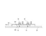
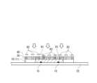
図11Aは、本実施形態に係る第2露出工程後の半導体基板の、図2AのX-X線における断面図である。図11Bは、本実施形態に係る第2露出工程後の半導体基板を模式的に示す上面図である。第2領域R2に対応する保護膜40および金属膜30が除去されて、第2領域R2に対応する半導体層11が露出している。図11Bでは、便宜的に保護膜40にハッチングを入れて示している。Figure 11A is a cross-sectional view of the semiconductor substrate after the second exposure step according to this embodiment, taken along line X-X in Figure 2A. Figure 11B is a top view that shows a schematic of the semiconductor substrate after the second exposure step according to this embodiment. The
(10)ダイシング工程(S10)
露出した第2領域に対応する半導体層を除去して、半導体基板を複数の素子チップに分割する。ダイシング工程は、金属膜の表面側から第2領域にプラズマ(第1のプラズマ)を照射することにより行うことができる。 (10) Dicing process (S10)
The semiconductor layer corresponding to the exposed second region is removed to divide the semiconductor substrate into a plurality of element chips. The dicing step can be performed by irradiating the second region with plasma (first plasma) from the front side of the metal film.
図12は、本実施形態に係るダイシング工程後の半導体基板の、図2AのX-X線における断面図である。第2領域R2に対応する半導体層11が除去されて、複数の素子チップ200が形成されている。Figure 12 is a cross-sectional view of the semiconductor substrate after the dicing process according to this embodiment, taken along line X-X in Figure 2A. The
ダイシング工程を行う前に、金属膜の表面を第2のプラズマによりクリーニングする工程を行ってもよい。第2のプラズマは、通常、ダイシングを行うときに発生させる第1のプラズマとは異なる条件で発生させる。このようなクリーニング工程は、例えば、第2露出工程に起因する残渣を低減する目的で行われる。これにより、より高品質のプラズマダイシングを行うことが可能になる。Before carrying out the dicing step, a step of cleaning the surface of the metal film with a second plasma may be carried out. The second plasma is usually generated under conditions different from the first plasma generated during dicing. Such a cleaning step is carried out, for example, for the purpose of reducing residues resulting from the second exposure step. This makes it possible to carry out plasma dicing of higher quality.
続いて、ダイシング工程で使用されるプラズマ処理装置の一実施形態を具体的に説明する。図13は、プラズマ処理装置の構造を概略的に示す断面図である。図13では、半導体基板が搬送キャリアに保持されている。プラズマ処理装置の構造は、これに限定されるものではない。Next, one embodiment of a plasma processing apparatus used in the dicing process will be specifically described. FIG. 13 is a cross-sectional view showing a schematic structure of the plasma processing apparatus. In FIG. 13, the semiconductor substrate is held by a transport carrier. The structure of the plasma processing apparatus is not limited to this.
(プラズマ処理装置)
プラズマ処理装置100は、ステージ111を備える。搬送キャリア20は、保持シート22の半導体基板10を保持している面が上方を向くように、ステージ111に載置される。ステージ111は、搬送キャリア20の全体を載置できる程度の大きさを備える。ステージ111の上方には、半導体基板10の少なくとも一部を露出させるための窓部124Wを有するカバー124が配置されている。カバー124には、フレーム21がステージ111に載置されている状態のとき、フレーム21を押圧するための押さえ部材107が配置されている。押さえ部材107は、フレーム21と点接触できる部材(例えば、コイルばねや弾力性を有する樹脂)であることが好ましい。これにより、フレーム21およびカバー124の熱が互いに影響し合うことを抑制しながら、フレーム21の歪みを矯正することができる。 (Plasma Processing Apparatus)
The
ステージ111およびカバー124は、真空チャンバ103内に配置されている。真空チャンバ103は、上部が開口した概ね円筒状であり、上部開口は蓋体である誘電体部材108により閉鎖されている。真空チャンバ103を構成する材料としては、アルミニウム、ステンレス鋼(SUS)、表面をアルマイト加工したアルミニウムなどが例示できる。誘電体部材108を構成する材料としては、酸化イットリウム(Y2O3)、窒化アルミニウム(AlN)、アルミナ(Al2O3)、石英(SiO2)などの誘電体材料が例示できる。誘電体部材108の上方には、上部電極としての第1の電極109が配置されている。第1の電極109は、第1の高周波電源110Aと電気的に接続されている。ステージ111は、真空チャンバ103内の底部側に配置される。 The
真空チャンバ103には、ガス導入口103aが接続されている。ガス導入口103aには、プラズマ発生用ガス(プロセスガス)の供給源であるプロセスガス源112およびアッシングガス源113が、それぞれ配管によって接続されている。また、真空チャンバ103には、排気口103bが設けられている。排気口103bには、真空チャンバ103内のガスを排気して減圧するための真空ポンプを含む減圧機構114が接続されている。真空チャンバ103内にプロセスガスが供給された状態で、第1の電極109に第1の高周波電源110Aから高周波電力が供給されることにより、真空チャンバ103内にプラズマが発生する。A
ステージ111は、それぞれ略円形の電極層115と、金属層116と、電極層115および金属層116を支持する基台117と、電極層115、金属層116、および基台117を取り囲む外周部118とを備える。外周部118は、導電性および耐エッチング性を有する金属により構成されており、電極層115、金属層116、および基台117をプラズマから保護する。外周部118の上面には、円環状の外周リング129が配置されている。外周リング129は、外周部118の上面をプラズマから保護する役割をもつ。電極層115および外周リング129は、例えば、上記の誘電体材料により構成される。The
電極層115の内部には、静電吸着(Electrostatic Chuck)用電極(以下、ESC電極119という。)と、第2の高周波電源110Bに電気的に接続された第2の電極120とが配置されている。ESC電極119には、直流電源126が電気的に接続されている。ESC電極119および直流電源126は、静電吸着機構を構成している。静電吸着機構によって、保持シート22はステージ111に押し付けられて固定される。以下、保持シート22をステージ111に固定する固定機構として、静電吸着機構を備える場合を例に挙げて説明するが、これに限定されない。保持シート22のステージ111への固定は、図示しないクランプによって行われてもよい。Inside the
金属層116は、例えば、表面にアルマイト被覆を形成したアルミニウムなどにより構成される。金属層116内には、冷媒流路127が形成されている。冷媒流路127は、ステージ111を冷却する。ステージ111が冷却されることにより、ステージ111に載置された保持シート22が冷却されると共に、ステージ111にその一部が接触しているカバー124も冷却される。これにより、半導体基板10や保持シート22が、プラズマ処理中に加熱されることによって損傷されることが抑制される。冷媒流路127内の冷媒は、冷媒循環装置125により循環される。The
ステージ111の外周付近には、ステージ111を貫通する複数の支持部122が配置されている。支持部122は、搬送キャリア20のフレーム21を支持する。支持部122は、第1の昇降機構123Aにより昇降駆動される。搬送キャリア20が真空チャンバ103内に搬送されると、所定の位置まで上昇した支持部122に受け渡される。支持部122の上端面がステージ111と同じレベル以下にまで降下することにより、搬送キャリア20は、ステージ111の所定の位置に載置される。A number of
カバー124の端部には、複数の昇降ロッド121が連結しており、カバー124を昇降可能にしている。昇降ロッド121は、第2の昇降機構123Bにより昇降駆動される。第2の昇降機構123Bによるカバー124の昇降の動作は、第1の昇降機構123Aとは独立して行うことができる。
制御装置128は、第1の高周波電源110A、第2の高周波電源110B、プロセスガス源112,アッシングガス源113、減圧機構114、冷媒循環装置125、第1の昇降機構123A、第2の昇降機構123B、および静電吸着機構を含むプラズマ処理装置100を構成する要素の動作を制御する。図14は、本実施形態で使用されるプラズマ処理装置のブロック図である。The
半導体基板10のエッチングは、半導体基板10が保持された搬送キャリア20を真空チャンバ103内に搬入し、半導体基板10がステージ111に載置された状態で行われる。半導体基板10の搬入の際、真空チャンバ103内では、昇降ロッド121の駆動により、カバー124が所定の位置まで上昇している。図示しないゲートバルブが開いて搬送キャリア20が搬入される。複数の支持部122は、上昇した状態で待機している。搬送キャリア20がステージ111上方の所定の位置に到達すると、支持部122に搬送キャリア20が受け渡される。搬送キャリア20は、保持シート22の粘着面22Xが上方を向くように、支持部122の上端面に受け渡される。The etching of the
搬送キャリア20が支持部122に受け渡されると、真空チャンバ103は密閉状態に置かれる。次に、支持部122が降下を開始する。支持部122の上端面が、ステージ111と同じレベル以下にまで降下することにより、搬送キャリア20は、ステージ111に載置される。続いて、昇降ロッド121が駆動する。昇降ロッド121は、カバー124を所定の位置にまで降下させる。このとき、カバー124に配置された押さえ部材107がフレーム21に点接触できるように、カバー124とステージ111との距離は調節されている。これにより、フレーム21が押さえ部材107によって押圧されると共に、フレーム21がカバー124によって覆われ、半導体基板10は窓部124Wから露出する。When the
カバー124は、例えば、略円形の外形輪郭を有したドーナツ形であり、一定の幅および薄い厚さを備える。窓部124Wの直径はフレーム21の内径よりも小さく、その外径はフレーム21の外径よりも大きい。したがって、搬送キャリア20をステージ111の所定の位置に搭載し、カバー124を降下させると、カバー124は、フレーム21を覆うことができる。窓部124Wからは、半導体基板10の少なくとも一部が露出する。The
カバー124は、例えば、セラミックス(例えば、アルミナ、窒化アルミニウムなど)や石英などの誘電体や、アルミニウムあるいは表面がアルマイト処理されたアルミニウムなどの金属で構成される。押さえ部材107は、上記の誘電体や金属の他、樹脂材料で構成され得る。The
搬送キャリア20が支持部122に受け渡された後、直流電源126からESC電極119に電圧を印加する。これにより、保持シート22がステージ111に接触すると同時にステージ111に静電吸着される。なお、ESC電極119への電圧の印加は、保持シート22がステージ111に載置された後(接触した後)に開始されてもよい。After the
エッチングが終了すると、真空チャンバ103内のガスが排出され、ゲートバルブが開く。複数の素子チップ200を保持する搬送キャリア20は、ゲートバルブから進入した搬送機構によって、プラズマ処理装置100から搬出される。搬送キャリア20が搬出されると、ゲートバルブは速やかに閉じられる。搬送キャリア20の搬出プロセスは、上記のような搬送キャリア20をステージ111に搭載する手順とは逆の手順で行われてもよい。すなわち、カバー124を所定の位置まで上昇させた後、ESC電極119への印加電圧をゼロにして、搬送キャリア20のステージ111への吸着を解除し、支持部122を上昇させる。支持部122が所定の位置まで上昇した後、搬送キャリア20は搬出される。When etching is completed, the gas in the
半導体層をエッチングするプラズマ(第1のプラズマ)の発生条件は、半導体層の材質などに応じて設定される。The conditions for generating the plasma (first plasma) that etches the semiconductor layer are set according to the material of the semiconductor layer, etc.
半導体層は、例えば、ボッシュプロセスによりプラズマエッチングされる。ボッシュプロセスでは、半導体層が深さ方向(厚さ方向)に垂直にエッチングされる。半導体層がSiを含む場合、ボッシュプロセスは、堆積ステップと、堆積膜エッチングステップと、Siエッチングステップとを順次繰り返すことにより、半導体層を深さ方向に掘り進む。The semiconductor layer is plasma etched, for example, by the Bosch process. In the Bosch process, the semiconductor layer is etched vertically in the depth direction (thickness direction). When the semiconductor layer contains Si, the Bosch process digs into the semiconductor layer in the depth direction by sequentially repeating a deposition step, a deposition film etching step, and a Si etching step.
堆積ステップは、例えば、プロセスガスとしてC4F8を150sccm以上、250sccm以下で供給しながら、真空チャンバ内の圧力を15Pa以上、25Pa以下に調整し、第1の高周波電源から第1の電極への投入電力を1500W以上、2500W以下として、第2の高周波電源から第2の電極への投入電力を0W以上、50W以下として、2秒以上、15秒以下、処理する条件で行われる。 The deposition step is performed underthe following conditions: for example,C4F8 is supplied as a process gas at 150 sccm or more and 250 sccm or less, the pressure in the vacuum chamber is adjusted to 15 Pa or more and 25 Pa or less, the power input from the first high frequency power supply to the first electrode is set to 1500 W or more and 2500 W or less, and the power input from the second high frequency power supply to the second electrode is set to 0 W or more and 50 W or less, and the processing time is 2 seconds or more and 15 seconds or less.
堆積膜エッチングステップは、例えば、プロセスガスとしてSF6を200sccm以上、400sccm以下で供給しながら、真空チャンバ内の圧力を5Pa以上、15Pa以下に調整し、第1の高周波電源から第1の電極への投入電力を1500W以上、2500W以下として、第2の高周波電源から第2の電極への投入電力を300W以上、1000W以下として、2秒以上、10秒以下、処理する条件で行われる。 The deposition film etching step is performed under the following conditions: for example, while supplyingSF6 as a process gas at 200 sccm or more and 400 sccm or less, the pressure inside the vacuum chamber is adjusted to 5 Pa or more and 15 Pa or less, the power input from the first high frequency power supply to the first electrode is set to 1500 W or more and 2500 W or less, and the power input from the second high frequency power supply to the second electrode is set to 300 W or more and 1000 W or less, and the processing time is 2 seconds or more and 10 seconds or less.
Siエッチングステップは、例えば、プロセスガスとしてSF6を200sccm以上、400sccm以下で供給しながら、真空チャンバ内の圧力を5Pa以上、15Pa以下に調整し、第1の高周波電源から第1の電極への投入電力を1500W以上、2500W以下として、第2の高周波電源から第2の電極への投入電力を50W以上、500W以下として、10秒以上、20秒以下、処理する条件で行われる。 The Si etching step is performed under the following conditions: for example, while supplyingSF6 as a process gas at 200 sccm or more and 400 sccm or less, the pressure inside the vacuum chamber is adjusted to 5 Pa or more and 15 Pa or less, the power input from the first high frequency power supply to the first electrode is set to 1500 W or more and 2500 W or less, and the power input from the second high frequency power supply to the second electrode is set to 50 W or more and 500 W or less, and the processing time is 10 seconds or more and 20 seconds or less.
上記のような条件で、堆積ステップ、堆積膜エッチングステップおよびSiエッチングステップを繰り返すことにより、Siを含む半導体層は、10μm/分以上、20μm/分以下の速度で深さ方向に垂直にエッチングされ得る。By repeating the deposition step, deposition film etching step, and Si etching step under the above conditions, the semiconductor layer containing Si can be etched vertically in the depth direction at a rate of 10 μm/min or more and 20 μm/min or less.
ここまで、ダイシング工程を備える素子チップの製造方法について説明してきたが、ダイシング工程に代えてエッチング工程を備える基板処理方法も、本実施形態に包含される。基板処理方法のエッチング工程では、第2露出工程の後、露出した第2領域に対応する半導体層をプラズマでエッチングする。このエッチング工程では、半導体基板は分割されず、分割領域に対応する溝が半導体基板に形成され得る。So far, we have described a method for manufacturing element chips that includes a dicing process, but this embodiment also includes a substrate processing method that includes an etching process instead of a dicing process. In the etching process of the substrate processing method, after the second exposure process, the semiconductor layer corresponding to the exposed second region is etched with plasma. In this etching process, the semiconductor substrate is not divided, and grooves corresponding to the division regions can be formed in the semiconductor substrate.
本開示は、素子チップの製造方法および基板処理方法に利用できる。This disclosure can be used in element chip manufacturing methods and substrate processing methods.
10:半導体基板
10a:ノッチ
10X:第1主面
10Y:第2主面
101:素子領域
102:分割領域
11:半導体層
15:アライメントマーク
R1:第1領域
R2:第2領域
20:搬送キャリア
21:フレーム
21a:ノッチ
21b:コーナーカット
22:保持シート
22X:粘着面
22Y:非粘着面
30:金属膜
40:保護膜
50:レジスト膜
100:プラズマ処理装置
103:真空チャンバ
103a:ガス導入口
103b:排気口
108:誘電体部材
109:第1の電極
110A:第1の高周波電源
110B:第2の高周波電源
111:ステージ
112:プロセスガス源
113:アッシングガス源
114:減圧機構
115:電極層
116:金属層
117:基台
118:外周部
119:ESC電極
120:第2の電極
121:昇降ロッド
122:支持部
123A:第1の昇降機構
123B:第2の昇降機構
124:カバー
124W:窓部
125:冷媒循環装置
126:直流電源
127:冷媒流路
128:制御装置
129:外周リング
200:素子チップ
300:赤外線カメラ10:
Claims (5)
Translated fromJapanese前記第2主面における前記アライメントマークに対応する第1領域をレジスト膜で被覆する被覆工程と、
前記第2主面上に金属膜を形成する金属膜形成工程と、
前記レジスト膜を除去し、前記第1領域に対応する前記半導体層を露出させる第1露出工程と、
前記金属膜の表面側から、前記半導体基板を、前記半導体層を透過する電磁波を感知するカメラにより撮像して、前記第1領域に対応する前記半導体層を通して前記アライメントマークの位置を検出し、検出された前記アライメントマークの位置に基づいて、前記金属膜の表面において前記分割領域に対応する第2領域を算出する算出工程と、
前記金属膜の表面側から前記第2領域に第1のレーザ光を照射して、前記第2領域に対応する前記金属膜を除去し、前記第2領域に対応する前記半導体層を露出させる第2露出工程と、
前記第2露出工程の後、露出した前記第2領域に対応する前記半導体層を除去して、前記半導体基板を複数の素子チップに分割するダイシング工程と、
を備える、素子チップの製造方法。 a preparation step of preparing a semiconductor substrate, the semiconductor substrate including a first layer having a first main surface including a plurality of element regions, division regions defining the element regions, and an alignment mark, and a second main surface opposite to the first main surface, the first layer including a semiconductor layer;
a coating step of coating a first area of the second main surface corresponding to the alignment mark with a resist film;
a metal film forming step of forming a metal film on the second main surface;
a first exposure step of removing the resist film to expose the semiconductor layer corresponding to the first region;
a calculation step of capturing an image of the semiconductor substrate from the surface side of the metal film by a camera that senses electromagnetic waves transmitted through the semiconductor layer, detecting a position of the alignment mark through the semiconductor layer corresponding to the first region, and calculating a second region on the surface of the metal film corresponding to the divided region based on the detected position of the alignment mark;
a second exposure step of irradiating the second region with a first laser light from a surface side of the metal film to remove the metal film corresponding to the second region and expose the semiconductor layer corresponding to the second region;
a dicing step of removing the semiconductor layer corresponding to the exposed second region after the second exposure step, and dividing the semiconductor substrate into a plurality of element chips;
A method for manufacturing an element chip comprising the steps of:
前記第2露出工程において、前記第2領域に対応する前記金属膜と共に前記第2領域に対応する前記保護膜を除去し、
前記ダイシング工程において、前記第2領域にプラズマを照射することにより、前記第2領域に対応する前記半導体層を除去する、請求項1に記載の素子チップの製造方法。 The method further includes a protective film forming step of forming a protective film that covers a surface of the metal film before the second exposure step,
In the second exposure step, the protective film corresponding to the second region is removed together with the metal film corresponding to the second region;
2. The method for producing element chips according to claim 1, wherein in the dicing step, the semiconductor layer corresponding to the second region is removed by irradiating the second region with plasma.
前記ダイシング工程を、前記半導体基板が前記保持シートに保持された状態で行う、請求項1または2に記載の素子チップの製造方法。 The method further includes a step of attaching the first main surface of the semiconductor substrate to a holding sheet prior to the dicing step,
3. The method for producing element chips according to claim 1, wherein the dicing step is performed in a state where the semiconductor substrate is held by the holding sheet.
前記第2主面における前記アライメントマークに対応する第1領域をレジスト膜で被覆する被覆工程と、
前記第2主面上に金属膜を形成する金属膜形成工程と、
前記レジスト膜を除去し、前記第1領域に対応する前記半導体層を露出させる第1露出工程と、
前記金属膜の表面側から、前記半導体基板を、前記半導体層を透過する電磁波を感知するカメラにより撮像して、前記第1領域に対応する前記半導体層を通して前記アライメントマークの位置を検出し、検出された前記アライメントマークの位置に基づいて、前記金属膜の表面において前記分割領域に対応する第2領域を算出する算出工程と、
前記金属膜の表面側から前記第2領域に第1のレーザ光を照射して、前記第2領域に対応する前記金属膜を除去し、前記第2領域に対応する前記半導体層を露出させる第2露出工程と、
前記第2露出工程の後、露出した前記第2領域に対応する前記半導体層をプラズマでエッチングするエッチング工程と、
を備える、基板処理方法。 a preparation step of preparing a semiconductor substrate, the semiconductor substrate including a first layer having a first main surface including a plurality of element regions, division regions defining the element regions, and an alignment mark, and a second main surface opposite to the first main surface, the first layer including a semiconductor layer;
a coating step of coating a first area of the second main surface corresponding to the alignment mark with a resist film;
a metal film forming step of forming a metal film on the second main surface;
a first exposure step of removing the resist film to expose the semiconductor layer corresponding to the first region;
a calculation step of capturing an image of the semiconductor substrate from the surface side of the metal film by a camera that senses electromagnetic waves transmitted through the semiconductor layer, detecting a position of the alignment mark through the semiconductor layer corresponding to the first region, and calculating a second region on the surface of the metal film corresponding to the divided region based on the detected position of the alignment mark;
a second exposure step of irradiating the second region with a first laser light from a surface side of the metal film to remove the metal film corresponding to the second region and expose the semiconductor layer corresponding to the second region;
an etching step of etching the semiconductor layer corresponding to the exposed second region with plasma after the second exposure step;
A substrate processing method comprising:
Priority Applications (2)
| Application Number | Priority Date | Filing Date | Title |
|---|---|---|---|
| JP2021091414AJP7641519B2 (en) | 2021-05-31 | 2021-05-31 | Manufacturing method of element chip and substrate processing method |
| US17/663,452US12300482B2 (en) | 2021-05-31 | 2022-05-16 | Element chip manufacturing method and substrate processing method |
Applications Claiming Priority (1)
| Application Number | Priority Date | Filing Date | Title |
|---|---|---|---|
| JP2021091414AJP7641519B2 (en) | 2021-05-31 | 2021-05-31 | Manufacturing method of element chip and substrate processing method |
Publications (2)
| Publication Number | Publication Date |
|---|---|
| JP2022183892A JP2022183892A (en) | 2022-12-13 |
| JP7641519B2true JP7641519B2 (en) | 2025-03-07 |
Family
ID=84194275
Family Applications (1)
| Application Number | Title | Priority Date | Filing Date |
|---|---|---|---|
| JP2021091414AActiveJP7641519B2 (en) | 2021-05-31 | 2021-05-31 | Manufacturing method of element chip and substrate processing method |
Country Status (2)
| Country | Link |
|---|---|
| US (1) | US12300482B2 (en) |
| JP (1) | JP7641519B2 (en) |
Families Citing this family (2)
| Publication number | Priority date | Publication date | Assignee | Title |
|---|---|---|---|---|
| JP2023119304A (en)* | 2022-02-16 | 2023-08-28 | 株式会社ディスコ | Substrate processing method |
| JP2024003614A (en)* | 2022-06-27 | 2024-01-15 | キヤノン株式会社 | Evaluation device, information processing device, program, film forming system, and article manufacturing method |
Citations (4)
| Publication number | Priority date | Publication date | Assignee | Title |
|---|---|---|---|---|
| JP2007133258A (en) | 2005-11-11 | 2007-05-31 | Fujifilm Corp | LAMINATE FOR PRINTED WIRING BOARD AND METHOD FOR PRODUCING PRINTED WIRING BOARD USING SAME |
| JP2013131653A (en) | 2011-12-21 | 2013-07-04 | Fujitsu Semiconductor Ltd | Semiconductor device and method for manufacturing the same |
| US20200243391A1 (en) | 2019-01-25 | 2020-07-30 | Semiconductor Components Industries, Llc | Backside metal patterning die singulation system and related methods |
| JP2020194918A (en) | 2019-05-29 | 2020-12-03 | パナソニックIpマネジメント株式会社 | Method for manufacturing element chip |
Family Cites Families (6)
| Publication number | Priority date | Publication date | Assignee | Title |
|---|---|---|---|---|
| JP4659300B2 (en)* | 2000-09-13 | 2011-03-30 | 浜松ホトニクス株式会社 | Laser processing method and semiconductor chip manufacturing method |
| US20060138681A1 (en) | 2004-12-27 | 2006-06-29 | Asml Netherlands B.V. | Substrate and lithography process using the same |
| US8299584B2 (en) | 2010-03-08 | 2012-10-30 | International Business Machines Corporation | Alignment of wafers for 3D integration |
| US8642448B2 (en) | 2010-06-22 | 2014-02-04 | Applied Materials, Inc. | Wafer dicing using femtosecond-based laser and plasma etch |
| JP5743958B2 (en)* | 2012-05-30 | 2015-07-01 | キヤノン株式会社 | Measuring method, exposure method and apparatus |
| JP2022175498A (en)* | 2021-05-13 | 2022-11-25 | パナソニックIpマネジメント株式会社 | Device chip manufacturing method and substrate processing method |
- 2021
- 2021-05-31JPJP2021091414Apatent/JP7641519B2/enactiveActive
- 2022
- 2022-05-16USUS17/663,452patent/US12300482B2/enactiveActive
Patent Citations (4)
| Publication number | Priority date | Publication date | Assignee | Title |
|---|---|---|---|---|
| JP2007133258A (en) | 2005-11-11 | 2007-05-31 | Fujifilm Corp | LAMINATE FOR PRINTED WIRING BOARD AND METHOD FOR PRODUCING PRINTED WIRING BOARD USING SAME |
| JP2013131653A (en) | 2011-12-21 | 2013-07-04 | Fujitsu Semiconductor Ltd | Semiconductor device and method for manufacturing the same |
| US20200243391A1 (en) | 2019-01-25 | 2020-07-30 | Semiconductor Components Industries, Llc | Backside metal patterning die singulation system and related methods |
| JP2020194918A (en) | 2019-05-29 | 2020-12-03 | パナソニックIpマネジメント株式会社 | Method for manufacturing element chip |
Also Published As
| Publication number | Publication date |
|---|---|
| US20220384177A1 (en) | 2022-12-01 |
| US12300482B2 (en) | 2025-05-13 |
| JP2022183892A (en) | 2022-12-13 |
Similar Documents
| Publication | Publication Date | Title |
|---|---|---|
| JP4544231B2 (en) | Manufacturing method of semiconductor chip | |
| JP7142236B2 (en) | Element chip manufacturing method | |
| JP5023614B2 (en) | Semiconductor chip manufacturing method and semiconductor wafer processing method | |
| CN108231676B (en) | Method for processing wafer | |
| US20220367273A1 (en) | Element chip manufacturing method and substrate processing method | |
| US11289428B2 (en) | Element chip manufacturing method | |
| US20130014905A1 (en) | Film peeling apparatus and film peeling method | |
| KR20040086725A (en) | Method for dividing semiconductor wafer | |
| JP2016506087A (en) | Laser-plasma etched wafer dicing using an etch chamber shield ring for film frame wafer applications | |
| JP6524553B2 (en) | Method of manufacturing element chip | |
| JP7641519B2 (en) | Manufacturing method of element chip and substrate processing method | |
| CN107204274A (en) | Method of plasma processing and plasma processing apparatus | |
| CN107452597B (en) | Manufacturing method of component chip | |
| JP6524558B2 (en) | Method of manufacturing element chip | |
| JP7281709B2 (en) | Element chip manufacturing method | |
| US10546783B2 (en) | Manufacturing process of element chip and substrate heating apparatus | |
| CN115547929A (en) | How the chip is made | |
| JP7292803B2 (en) | Wafer processing method | |
| JP7316638B2 (en) | Method for manufacturing resin composition, resin-coated substrate and element chip | |
| JP7390615B2 (en) | Resin coating equipment, resin film forming method, and device chip manufacturing method | |
| JP2020196023A (en) | Laser machining equipment, laser machining method, and device chip manufacturing method | |
| JP2018056486A (en) | Mask forming method and wafer processing method | |
| KR20240043690A (en) | Method for processing device wafer | |
| JP2025039183A (en) | Processing method | |
| KR20240002926A (en) | Method for processing a device wafer |
Legal Events
| Date | Code | Title | Description |
|---|---|---|---|
| A621 | Written request for application examination | Free format text:JAPANESE INTERMEDIATE CODE: A621 Effective date:20240308 | |
| A977 | Report on retrieval | Free format text:JAPANESE INTERMEDIATE CODE: A971007 Effective date:20241226 | |
| TRDD | Decision of grant or rejection written | ||
| A01 | Written decision to grant a patent or to grant a registration (utility model) | Free format text:JAPANESE INTERMEDIATE CODE: A01 Effective date:20250114 | |
| A61 | First payment of annual fees (during grant procedure) | Free format text:JAPANESE INTERMEDIATE CODE: A61 Effective date:20250210 | |
| R150 | Certificate of patent or registration of utility model | Ref document number:7641519 Country of ref document:JP Free format text:JAPANESE INTERMEDIATE CODE: R150 |