JP7638735B2 - Electronics - Google Patents
ElectronicsDownload PDFInfo
- Publication number
- JP7638735B2 JP7638735B2JP2021037180AJP2021037180AJP7638735B2JP 7638735 B2JP7638735 B2JP 7638735B2JP 2021037180 AJP2021037180 AJP 2021037180AJP 2021037180 AJP2021037180 AJP 2021037180AJP 7638735 B2JP7638735 B2JP 7638735B2
- Authority
- JP
- Japan
- Prior art keywords
- power
- electronic device
- switch
- input
- stored
- Prior art date
- Legal status (The legal status is an assumption and is not a legal conclusion. Google has not performed a legal analysis and makes no representation as to the accuracy of the status listed.)
- Active
Links
Images


Classifications
- Y—GENERAL TAGGING OF NEW TECHNOLOGICAL DEVELOPMENTS; GENERAL TAGGING OF CROSS-SECTIONAL TECHNOLOGIES SPANNING OVER SEVERAL SECTIONS OF THE IPC; TECHNICAL SUBJECTS COVERED BY FORMER USPC CROSS-REFERENCE ART COLLECTIONS [XRACs] AND DIGESTS
- Y02—TECHNOLOGIES OR APPLICATIONS FOR MITIGATION OR ADAPTATION AGAINST CLIMATE CHANGE
- Y02D—CLIMATE CHANGE MITIGATION TECHNOLOGIES IN INFORMATION AND COMMUNICATION TECHNOLOGIES [ICT], I.E. INFORMATION AND COMMUNICATION TECHNOLOGIES AIMING AT THE REDUCTION OF THEIR OWN ENERGY USE
- Y02D10/00—Energy efficient computing, e.g. low power processors, power management or thermal management
Landscapes
- Power Sources (AREA)
- Facsimiles In General (AREA)
Description
Translated fromJapanese本発明は、ファクシミリ機能等を有する画像形成装置等の電子機器に関するものである。The present invention relates to electronic devices such as image forming devices that have facsimile functions, etc.
従来の電子機器、例えばファクシミリ機能を有する複合機(画像形成装置)には、急な停電等により異常終了した後で停電状態が解消された場合に、停電前の状態まで、もしくはスタンバイ状態まで、自動的に復帰する機能を有するものがある。Some conventional electronic devices, such as multifunction peripherals (image forming devices) with facsimile functions, have a function that automatically restores the device to the state before the power outage or to a standby state when the power outage is resolved after the device has abnormally shut down due to a sudden power outage or other reason.
特許文献1には、前回の商用電源供給が停止する直前の動作状態を不揮発メモリに記憶させ、次に商用電源供給が再開された際に、前記不揮発メモリのデータを読み取ることによって複合機を自動復帰させるかどうかを切り替える技術が開示されている。すなわち、不揮発メモリに記録されているデータにより、前回の電源供給停止前に複合機が正常終了されていないことを認識した場合は、使用者が電源スイッチを押すことなく複合機を再起動させる技術が開示されている。Patent Document 1 discloses a technique for storing in non-volatile memory the operating state immediately before the previous interruption of commercial power supply, and then, when commercial power supply is resumed, reading the data in the non-volatile memory to switch whether or not the multifunction device should automatically return to normal. In other words, if it is recognized from the data stored in the non-volatile memory that the multifunction device was not shut down normally before the previous power supply interruption, the technique discloses a technique for restarting the multifunction device without the user having to press the power switch.
また、特許文献2には、例えば製造工程で正常終了されなかった場合に、複合機が出荷・納品されて最初に複合機の電源プラグが電源コンセントに挿されたときに複合機が再起動してしまうことを防止する技術が開示されている。不揮発メモリを用いるところは特許文献1と同様であるが、特許文献2には、加えて電源が切れてから所定時間以上経過したかどうかを認識する手段が設けられている。特許文献2では、正常終了していない場合でも所定時間以上経過していた場合は複合機を再起動させないようにしている。これは、製造工程から出荷後にユーザ先に納品されるまでには相当の時間が経過していることを想定したものである。Patent Document 2 also discloses a technique for preventing a multifunction device from restarting when the power plug of the multifunction device is first inserted into a power outlet after it is shipped and delivered, for example, if the manufacturing process has not ended normally. The use of non-volatile memory is similar to Patent Document 1, but Patent Document 2 also includes a means for recognizing whether a predetermined time has passed since the power was turned off. Patent Document 2 prevents the multifunction device from restarting if a predetermined time has passed, even if the device has not ended normally. This is based on the assumption that a considerable amount of time has passed between the manufacturing process and delivery to the user after shipping.
しかし、従来の構成では、以下に示すように意図しない停電復帰動作(上述した自動で復帰する動作)を確実に防ぐことができないという課題があった。その課題について図10を用いて説明する。However, the conventional configuration had the problem that it was not possible to reliably prevent unintended power failure recovery operations (the automatic recovery operations described above), as shown below. This problem will be explained using Figure 10.
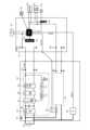
図10は、従来の画像形成装置内の電気構成の一部を抽出したブロック図である。
商用電源20は、不図示の電源コンセントを介して電力を供給する。電源基板21は、電源コンセントに電源プラグが挿されて電源ケーブルを介して商用電源20に接続されたことにより電力が供給されると、画像形成装置内で使用するDC電圧を生成する。電源基板21には、容量が大きい平滑用の電解コンデンサ22が接続されている。 FIG. 10 is a block diagram showing a part of the electrical configuration in a conventional image forming apparatus.
The
DCコントローラ基板23は、画像形成装置の各種制御を行う。DCコントローラ基板23は、CPU24、不揮発メモリ25を有する。CPU24には、不揮発メモリ25がアクセス可能に接続されている。また、DCコントローラ基板23には、電源スイッチ(SW)26が接続されている。電源スイッチ26は、該電源スイッチ26が操作された場合に、そのことをCPU24が検出することが可能なように接続されている。The
商用電源が供給されている場合、電源基板21からDC電圧(3.3V)が出力され、コントローラ基板23に供給される。
電源スイッチ26が押されたことを検知すると、CPU24は、画像形成装置の各部を起動するとともに、不揮発性メモリ25に電源ONされたことを示す情報“電源ONフラグ”を記憶させ、画像形成装置をスタンバイ状態にする。 When commercial power is supplied, a DC voltage (3.3 V) is output from the
When the
次に、スタンバイ状態で電源スイッチ26を押されたことを検知すると、CPU24は、所定のシャットダウン処理を行った後に不揮発性メモリ25に正常終了したことを記録(前述の“電源ONフラグ”を解除)した後に画像形成装置をオフ状態にする。Next, when it detects that the
なお、画像形成装置がオフ状態となった後に電源コンセントから電源プラグを抜き、商用電源の供給が停止された場合でも、電源基板21内の電解コンデンサ22にはしばらくの間電荷が残っている。そのため、電解コンデンサ22に電荷が残っている間は、DC電圧(3.3V)が電源基板21から出力され、コントローラ基板23に供給され続ける。この場合、画像形成装置の電力消費は非常に小さいため平滑用の電解コンデンサ22の放電がなかなか進まず、数分(5~10分)程度この状態が継続することになる。Even if the power plug is removed from the power outlet after the image forming apparatus has been turned off and the supply of commercial power is stopped, a charge remains in the
この状態で、誤ってユーザが電源スイッチ26を押してしまうと、CPU24は、画像形成装置の起動処理を開始するとともに不揮発性メモリ25に“電源ONフラグ“を記録する。しかし、起動処理により消費電力が増加するため、電解コンデンサ22は短時間(数百msec程度)で放電してしまい、DC電圧の供給が途絶え、強制的にシャットダウンされることになる。この場合、CPU24は、不揮発性メモリ25に記憶された”電源ONフラグ“を解除することができないため、”電源ONフラグ“が記録されたままとなってしまう。In this state, if the user accidentally presses the
その後、電源コンセントに電源プラグを再度接続し商用電源供給が再開されると、電源基板21からはDC電圧(3.3V)がDCコントローラ基板23に供給され、CPU24が起動する。該起動したCPU24は、不揮発性メモリ25にアクセスし、”電源ONフラグ“が残っていることを認識すると、前回は停電などの原因により異常終了したものと判断して、画像形成装置が意図せずに再起動してしまう。これは、ユーザ観点では意図しない動作であり、望ましいものではない。
なお、各種電子機器(家電等も含む)にも上述のような停電復帰機能を有するものがあり、このような電子機器でも共通の課題であった。
このように従来の電子機器では、意図しない停電復帰動作を確実に防ぐことができないという課題があった。 Thereafter, when the power plug is reconnected to the power outlet and commercial power supply is resumed, DC voltage (3.3 V) is supplied from the
It should be noted that various electronic devices (including home appliances) also have the above-mentioned power failure recovery function, and this problem is common to such electronic devices as well.
Thus, conventional electronic devices have a problem in that they cannot reliably prevent unintended power failure recovery operations.
本発明は、上記の課題を解決するためになされたものである。本発明は、ユーザの意図しない停電復帰動作を確実に防ぐことができる仕組みを提供することを目的とするものである。The present invention has been made to solve the above problems. The purpose of the present invention is to provide a mechanism that can reliably prevent power outage recovery operations unintentionally by the user.
本発明は、電子機器であって、前記電子機器を制御する制御手段と不揮発性の記憶手段とを備える制御部と、第1電力が入力された状態で前記第1電力からコンデンサを介して第2電力を生成し、前記第2電力を前記制御部に供給するものであり、前記第1電力の入力がなくなっても前記コンデンサの電荷により前記第2電力の供給が可能な電源手段と、ユーザが前記電子機器の起動を指示するためのスイッチと、を有し、前記制御手段は、前記スイッチの操作なしに前記電源手段から前記制御部への前記第2電力の供給が再開された場合、前記記憶手段に電力の供給に係る所定情報が記憶されている場合には前記電子機器の起動を開始し、前記記憶手段に前記所定情報が記憶されていない場合には前記電子機器の起動を行わないよう制御し、前記電子機器がシャットダウン状態から前記スイッチの操作により前記起動が指示された場合に所定時間以上経過した後に前記記憶手段に前記所定情報を記憶し、前記所定情報が記憶されている状態で前記スイッチの操作により前記電子機器のシャットダウンが正常に終了した場合に前記記憶手段から前記所定情報を消去するものであり、前記所定情報は前記スイッチが操作されて前記電子機器の電源がオンされたことを示す情報であり、前記所定時間は、前記第1電力が入力されていない状態で前記スイッチが操作されてから前記第2電力が前記制御手段へ供給されなくなるまでの時間に対応する時間以上の時間であることを特徴とする。 The present invention relates to an electronic device, comprising: a control unit including a control means for controlling the electronic device and a non-volatile storage means; power supply means for generating a second power from a first powervia a capacitor when the first power is input, and supplying the second power to the control unit, the power supply means being capable of supplying the second power by the charge of the capacitor even when the input of the first power is no longer input ; and a switch for a user to instruct startup of the electronic device, the control means starting the startup of the electronic device when the supply of the second power from the power supply means to the control unit is resumed without the operation of the switch, if predetermined information related to the supply of power is stored in the storage means, and starting the startup of the electronic device when the predetermined information is not stored in the storage means. In this case, the electronic device is controlled not to be started up, and when the startup ofthe electronic device is instructed by operating the switch from a shutdown state, the specified information is stored in the storage means after a specified timehas elapsed , and when shutdown of the electronic device is normally completed by operating the switch while the specified information is stored, the specified informationisinformation indicating that the switch has been operated to turn on the power of the electronic device, and the specified time is a time equal to or longer than the time corresponding to the time from when the switch is operated when the first power is not input to when the second power is no longer supplied to the control means .
本発明によれば、ユーザの意図しない停電復帰動作を確実に防ぐことができる。This invention can reliably prevent the user from unintentionally performing power outage recovery operations.
以下に、図面を参照して、この発明の実施の形態を例示的に詳しく説明する。ただし、この実施の形態に記載されている構成要素はあくまで例示であり、この発明の範囲をそれらのみに限定するものではない。Below, an embodiment of the present invention will be described in detail with reference to the drawings. However, the components described in this embodiment are merely examples, and the scope of the present invention is not limited to them.
〔第1実施形態〕
図1は、本発明の第1実施形態を示す電子機器の一例を示す画像形成装置の電気構成の一部を抽出したブロック図である。 First Embodiment
FIG. 1 is a block diagram showing a part of the electrical configuration of an image forming apparatus as an example of an electronic device according to a first embodiment of the present invention.
商用電源120は、不図示の電源コンセントを介して商用電源(AC100V)を供給する。電源基板(電源ユニット)121は、電源コンセントに電源プラグが挿されて電源ケーブルを介して商用電源120に接続されたことにより電力が供給されると、画像形成装置内で使用するDC電圧を生成する。電源基板121に供給された商用電源は、第一のAC/DCコンバータ回路130に入力される。供給された商用電源は、第一のAC/DCコンバータ回路130に入力された後、整流回路125で整流され、平滑用の電解コンデンサ126で平滑される。スイッチングFET127、絶縁トランス128、整流・平滑回路129を介してDC電圧(3.3V)が生成される。このDC電圧は、比較回路131と制御IC132によりフィードバックされた周波数、デューティー比でスイッチングFET127をスイッチングすることにより3.3Vに安定して制御される。このDC電圧(3.3V)は、商用電源120が供給されている状態では、第一のAC/DCコンバータ回路130から常に出力される構成となっている。The
第二のAC/DCコンバータ123は、画像形成装置内の駆動モーターや画像形成に使用する高圧電源を駆動するための比較的大きな電力を賄うDC電圧(24V)を生成する回路である。第二のAC/DCコンバータ123の内部回路の構成は、第一のAC/DCコンバータ回路130と同様である。第二のAC/DCコンバータ123への商用電源供給は、リレー124により制御される。画像形成装置本体が省電力モードの時やシャットダウン状態などの場合に、無駄な電力消費を防止するために、リレー124により第二のAC/DCコンバータ123への商用電源の供給を遮断する機能を有している。The second AC/
DCコントローラ基板101は、画像形成装置における各動作の制御を行っている制御部である。DCコントローラ基板101は、画像形成装置内の各負荷動作の制御を担っている。
CPU102には、不揮発メモリ(EEPROM)103が接続されており、メモリ内に任意のデータを読み書きすることが可能である。CPU102は、不揮発性メモリ103又はその他の不図示のROM等に格納されたプログラムを読み出して実行することにより各種制御を行う。 The
A non-volatile memory (EEPROM) 103 is connected to the
電源スイッチ104は、画像形成装置の外装にユーザが操作可能なように取り付けられており、操作されたことを検知できるようにCPU102に電気的に接続されている。なお、画像形成装置がシャットダウンされた状態で電源スイッチ104を操作することにより、ユーザは画像形成装置の起動を指示することができる。また、画像形成装置が起動状態(スタンバイ状態等)で電源スイッチ104を操作することにより、ユーザは画像形成装置のシャットダウンを指示することができる。The
モータードライバIC(M-Drv)105は、画像形成装置を動作させるためのモーター106を駆動する機能を有し、CPU102の制御の基に24Vが供給された状態でモーター106を駆動することが可能である。
高圧基板107は、画像形成動作に必要な高圧電源電圧を生成する機能を有しており、CPU102の制御の基に24Vが供給された状態で動作することが可能である。
操作部ユニット108は、ユーザが画像形成装置を操作するための操作キーや液晶表示部を有している。操作部ユニット108は、CPU102の制御の基に、24Vが供給された状態で動作することが可能である。 A motor driver IC (M-Drv) 105 has a function of driving a
The high-
The
センサ109は、画像形成装置内の用紙位置を検知するためのセンサである。実際の画像形成装置においては、複数のモーター、センサ、その他の基板がDCコントローラ基板101に接続されている。しかし、図1においては説明を簡潔にするために、DCコントローラ基板101に接続される各負荷の一部のみを示している。
図2は、画像形成装置の電源プラグを電源コンセントに挿してからの電源状態の遷移の一例を示すタイミングチャートである。
タイミングT1で電源プラグを電源コンセントに挿すと、商用電源120から電源ケーブルを介して電源基板121に対して電力が供給され、電源基板121で3.3V電圧が作られ、DCコントローラ基板101に供給される。3.3VがDCコントローラ基板101内のCPU102に供給されることにより、CPU102が起動する。 FIG. 2 is a timing chart showing an example of the transition of the power state after the power plug of the image forming apparatus is inserted into the power outlet.
When the power plug is inserted into the power outlet at timing T1, power is supplied from
タイミングT2で電源スイッチ104が押されたことをCPU102が検知(即ち起動指示を検知)すると、タイミングT3で24V_ON信号が出力され、リレー124がONされ、タイミングT4で24V電圧が生成される。24Vは各基板や負荷に供給され、画像形成装置全体が起動状態となる。When the
次に、タイミングT5で電源スイッチ104が押されると、画像形成装置は各基板や負荷のシャットダウン処理を行い、タイミングT6で24V_ON信号を反転させてリレー124をOFFすることにより24V出力を停止させ、装置をシャットダウンする。この時点で3.3Vは正常に出力され続けており、CPU102の動作状態も継続している。Next, when the
図3は、画像形成装置がシャットダウンされた状態で電源プラグを電源コンセントから抜いた場合の電源状態遷移の一例を示すタイミングチャートである。
タイミングT7で電源プラグを電源コンセントから抜くと、商用電源120からの電力供給は停止するが、平滑用の電解コンデンサ126が大容量であるため数分(例えば5~10分)程度3.3V電圧が出力され続ける。すなわち、電源基板121では、電解コンデンサ126に蓄えられている電荷を電源として3.3V電圧が生成される。電解コンデンサ126がある程度放電されたタイミング(T8)で3.3Vの出力が停止し、CPU102も停止状態となる。 FIG. 3 is a timing chart showing an example of power state transition when the power plug is unplugged from the power outlet while the image forming apparatus is shut down.
When the power plug is removed from the power outlet at timing T7, the power supply from
図4は、画像形成装置がシャットダウン(電源オフ)された状態で電源プラグを電源コンセントから抜いた直後に電源スイッチを押した場合の電源状態遷移の一例を示すタイミングチャートである。
タイミングT7で電源プラグを抜き、その直後のタイミング(T9)で電源スイッチ104が押されると、CPU102が未だ動作状態であるため、24V_ON信号がタイミングT10でONとなる。これにより、タイミングT11で24Vが出力され画像形成装置の起動動作が開始される。 FIG. 4 is a timing chart showing an example of power state transition when the power switch is pressed immediately after the power plug is removed from the power outlet while the image forming apparatus is shut down (powered off).
When the power plug is pulled out at timing T7 and the
しかし、この起動動作で電力消費が増加するため、電解コンデンサ126が速やかに放電され、3.3V、24Vとも、短時間(例えば100~200msec程度)で出力が停止し(タイミングT12)、画像形成装置本体が強制的にシャットダウンされる。
図4内の所定時間Tdは、電源プラグが抜かれている状態で、電源スイッチ104が押されてからシャットダウン状態になるまでの時間を示しており、例えば100~200msec程度となる。すなわち、所定時間Tdは、商用電源の入力が断たれた状態で電源スイッチ104が押されてからDC電圧(3.3V、24V)の供給がなくなるまでの時間に対応するとも言える。 However, since this startup operation increases power consumption, the
4 indicates the time from when the
図5は、電源コンセントに電源プラグを挿した場合の動作を説明するためのフローチャートである。このフローチャートの処理は、CPU102が不揮発性メモリ103又はその他の不図示のROM等に格納されたプログラムを読み出して実行することにより実現される。Figure 5 is a flowchart for explaining the operation when the power plug is inserted into the power outlet. The processing of this flowchart is realized by the
電源プラグを電源コンセントに挿すことによりCPU102に3.3V電圧の供給が開始(再開)され、CPU102が起動する(S501)。
S502において、CPU102は、不揮発性メモリ103の所定アドレスにある電源ONフラグを確認し“1”が立っているか否かを判定する。なお、電源ONフラグは、不揮発性メモリ103の所定アドレスに、電源ONされたことを示す所定情報として記憶され(“1”が記憶される)、正常終了した場合に解除(消去)される(“0”が記憶される)ものである。 When the power plug is inserted into the power outlet, the supply of 3.3V voltage to the
In S502, the
電源ONフラグに“1”が立っている場合(S502でYesの場合)、CPU102は、S503に処理を進める。
S503では、CPU102は、画像形成装置の起動処理を開始する。
次にS504において、CPU102は、起動処理の終了を待つ。起動処理が終了すると(S504でYesとなると)、CPU102は、S505に処理を進め、スタンバイ状態に移行する。 If the power ON flag is set to "1" (Yes in S502), the
In S503, the
Next, in S504, the
一方、電源ONフラグに“1”が立っていない場合(S502でNoの場合)、CPU102は、画像形成装置を起動せずにS506に処理を進め、シャットダウン状態に移行する。On the other hand, if the power ON flag is not set to "1" (No in S502), the
図6は、画像形成装置がスタンバイ状態の時に電源スイッチ104が押された場合の動作(停電復帰動作)を説明するためのフローチャートである。このフローチャートの処理は、CPU102が不揮発性メモリ103又はその他の不図示のROM等に格納されたプログラムを読み出して実行することにより実現される。Figure 6 is a flowchart for explaining the operation (power failure recovery operation) when the
スタンバイ状態の時に電源スイッチ104が押されると(S601)、CPU102は、それを検知し、S602に処理を進める。
S602では、CPU102は、シャットダウン処理を実行し、シャットダウン処理が終了すると(S602でYesになると)、S603に処理を進める。 When the
In S602, the
S603では、CPU102は、24V_ON信号をOFFにする。
次にCPU102は、S604において、不揮発性メモリ103の所定アドレスに書き込まれている電源ONフラグを“0”に更新し、S605において、シャットダウン状態に移行する。 In S603, the
Next, in S604, the
図7は、第1実施形態の画像形成装置がシャットダウン状態の時に電源スイッチが押された場合の動作を説明するためのフローチャートである。このフローチャートの処理は、CPU102が不揮発性メモリ103又はその他の不図示のROM等に格納されたプログラムを読み出して実行することにより実現される。Figure 7 is a flowchart for explaining the operation when the power switch is pressed while the image forming apparatus of the first embodiment is in a shutdown state. The processing of this flowchart is realized by the
シャットダウン状態の時に電源スイッチ104が押されると(S701)、CPU102は、それを検知し、S702に処理を進める。
S702では、CPU102は、24V_ON信号をONし、電源から24V電圧を出力させる。 When the
In S702, the
次にS703において、CPU102は、画像形成装置の起動処理を開始する。
次にCPU102は、S704において、所定時間Td経過した後にS705に処理を進めるように制御する。所定時間Tdは、図4に示したように、商用電源の入力が断たれた状態でスイッチ104の操作により画像形成装置の起動が指示されてからDC電圧(3.3V)のCPU102への供給がなくなるまでの時間に対応する。よって、電源プラグが抜かれている状態で電源スイッチ104が押された場合には、S704で所定時間Tdの経過を判断している間にCPU102への電力供給が断たれ、S705以降の処理は実行されないことになる。 Next, in step S703, the
Next, the
CPU102は、所定時間Td経過した(S704でYesとなった)後に、S705において、不揮発性メモリ(103)の所定アドレスに電源ONフラグ=1を書き込む。なお、上記S704で待機する時間はTdに限定されるものではなくTd以上の時間であればよい。After a predetermined time Td has elapsed (S704 becomes Yes), in S705, the
次にCPU102は、S706において、画像形成装置の起動処理終了を待ち、起動処理が終了したら(S706でYesとなったら)後に、S707において、スタンバイ状態に移行する。Next, in S706, the
本実施形態では、図7のS704で所定時間以上経過した後にS705の処理(“電源ONフラグ”を立てる)を実行するように構成する。これにより、電源プラグが抜かれている状態(商用電源の入力が断たれた状態)で電源スイッチ104が誤って押された場合でも、S705で電源ONフラグに“1”を書き込む前に3.3V電圧の供給が停止し、シャットダウンする。このため、次に電源プラグが挿された際に図5のS502で電源ONフラグが“0”となっているため、意図せずに画像形成装置が起動してしまうことを防止することができる。なお、本実施形態では、平滑用の電解コンデンサ126を急速放電する回路などを追加する必要がなく、基板の大型化やコストアップすることもなく、意図せずに画像形成装置が起動してしまうことを防止するという課題を解決することができる。In this embodiment, the process of S705 (setting the "power ON flag") is executed after a predetermined time or more has elapsed in S704 in FIG. 7. As a result, even if the
〔第2実施形態〕
図8は、本発明の第2実施形態を示す画像形成装置の電気構成の一部を抽出したブロック図である。第2実施形態で示す図8と第1実施形態で示した図1との差異は、ゼロクロス検知回路801の有無であり、図1と同一のものには同一の符号を付してある。 Second Embodiment
Fig. 8 is a block diagram showing a part of the electrical configuration of an image forming apparatus according to a second embodiment of the present invention. The difference between Fig. 8 showing the second embodiment and Fig. 1 showing the first embodiment is the presence or absence of a zero-
ゼロクロス検知回路(ZC)801は、商用電源120から供給されるAC電圧が0Vとなるタイミングで出力が反転するZEROX信号を生成する回路である。例えば、供給されている商用電源が100V/50Hzの場合、ZEROX信号として50Hzの矩形波を出力する。また、電源プラグが電源コンセントから抜かれている場合にはZEROX信号は生成されない。なお、ZEROX信号は、CPU102で検出可能なように接続されている。The zero-cross detection circuit (ZC) 801 is a circuit that generates a ZEROX signal whose output is inverted when the AC voltage supplied from the
図9は、第2実施形態の画像形成装置がシャットダウン状態の時に電源スイッチが押された場合の動作を説明するためのフローチャートである。このフローチャートの処理は、CPU102が不揮発性メモリ103又はその他の不図示のROM等に格納されたプログラムを読み出して実行することにより実現される。
なお、図7と同一のステップには同一のステップ番号を付してあり、説明を省略する。 9 is a flowchart for explaining the operation when the power switch is pressed while the image forming apparatus according to the second embodiment is in a shutdown state. The processing of this flowchart is realized by the
The same steps as those in FIG. 7 are given the same step numbers, and the explanation thereof will be omitted.
第2実施形態では、S703において画像形成装置の起動処理を開始した後、CPU102は、S901に処理を進める。
S901では、CPU102は、ZEROX信号が入力されているかどうかを検知する。ZEROX信号が入力されている場合(S901でYesの場合)、CPU102は、商用電源が入力されている状態と判断し、S705に処理を進め、電源ONフラグ=1を書き込む。 In the second embodiment, after starting the startup process of the image forming apparatus in step S703, the
In S901, the
一方、ZEROX信号が検出されない場合(S901でNoの場合)、CPU102は、商用電源の入力が断たれた状態と判断し、電源ONフラグ=1を書き込むことなく、S902に処理を進める。
S902では、CPU102は、所定時間Td(第1実施形態のTdと同じ時間)経過後にS903に処理を進めるように制御する。CPU102は、所定時間Td経過した(S902でYesとなった)後に、S903において、ZEROX信号が異常であることを示すエラーを表示(通知)する。 On the other hand, if the ZEROX signal is not detected (No in S901), the
In S902, the
上述のように、S902で所定時間Td待つことにより、電源プラグが抜かれていた場合にはエラー検知する前に3.3V電圧及び24V電圧の供給が停止し、画像形成装置本体がシャットダウンするため、誤ってエラーを検知することを防止できる。なお、上記S902で待機する時間はTdに限定されるものではなくTd以上の時間であればよい。
なお、電源コンセントに電源プラグを接続して商用電源の供給が開始されるときの動作フローチャートは、第1実施形態で示した図5と同じである。 As described above, by waiting for the predetermined time Td in S902, if the power plug is unplugged, the supply of 3.3V and 24V voltages is stopped and the image forming apparatus main body is shut down before an error is detected, thereby preventing erroneous error detection. Note that the waiting time in S902 is not limited to Td, and may be any time equal to or greater than Td.
The operation flowchart when the power plug is connected to the power outlet and the supply of commercial power is started is the same as that shown in FIG. 5 in the first embodiment.
第2実施形態においては、電源プラグが抜かれている状態で電源スイッチ104が誤って押されたしまったとしても、S901でZEROX信号が検出されない場合にはS705の書き込み動作を行うことがない。このため、次に電源プラグが挿された際に図5のS502で電源ONフラグが“0”となっているため意図せずに画像形成装置が起動してしまうことを防止することができる。In the second embodiment, even if the
上記各実施形態では、商用電源120の電源コンセントに対して画像形成装置の電源ケーブルの電源プラグを挿す/抜く場合を例にして説明した。なお、画像形成装置本体に対して電源ケーブル挿す/抜くことが可能な構成の場合、商用電源120の電源コンセントに画像形成装置の電源ケーブルの電源プラグを挿した状態で画像形成装置本体に対して電源ケーブル挿す/抜く場合も同様である。In each of the above embodiments, the case where the power plug of the power cable of the image forming apparatus is inserted/removed from the power outlet of the
第1実施形態では、電源スイッチ104が押されたことを検知してから不揮発性メモリに“電源ONフラグ”をセットするタイミングを所定時間以上遅らせる構成について説明した。また、第2実施形態では、電源スイッチ104が押されたことを検知した場合であってZEROX信号が検出された場合に不揮発性メモリに“電源ONフラグ”をセットし、ZEROX信号が検出されない場合にセットしない構成について説明した。なお、第2実施形態はZEROX信号の検出に限定されるものではなく、商用電源120の入力の有無を検出可能な手段であれば、どのような手段を用いてもよい。
また、本発明はこれらの構成に限定されるものではなく、商用電源120が入力されていない状態で電源スイッチ104が押された場合、不揮発性メモリに“電源ONフラグ”を書き込まない制御を実現可能な構成であれば、どのような方法を用いてもよい。 In the first embodiment, a configuration was described in which the timing of setting the "power ON flag" in the non-volatile memory is delayed by a predetermined time or more after it is detected that the
Furthermore, the present invention is not limited to these configurations, and any method may be used as long as it is possible to realize control that does not write a “power ON flag” to non-volatile memory when
以上各実施形態によれば、電源プラグがコンセントから抜かれて間もない状態で電源スイッチを押された場合に、再度シャットダウンされてしまう前に不揮発性メモリに“電源ONフラグ”が記憶されてしまうことを防止することができる。したがって、次に商用電源の供給が再開された際に、意図しない場合は停電復帰動作をしないようにすることができる。
また、本発明は、画像形成装置に限定されるものではなく、家電等も含む各種電子機器にも適用可能であり、ユーザの意図しない機器の停電復帰動作を防ぐことができる。 According to each of the above embodiments, when the power switch is pressed immediately after the power plug is unplugged from the outlet, it is possible to prevent the "power ON flag" from being stored in the non-volatile memory before the device is shut down again. Therefore, when the supply of commercial power is resumed next time, it is possible to prevent the device from performing an unintended power outage recovery operation.
Furthermore, the present invention is not limited to image forming apparatuses, but can also be applied to various electronic devices including home appliances, and can prevent the device from performing a power outage recovery operation unintended by the user.
なお、上述した各種データの構成及びその内容はこれに限定されるものではなく、用途や目的に応じて、様々な構成や内容で構成されることは言うまでもない。
以上、一実施形態について示したが、本発明は、例えば、システム、装置、方法、プログラムもしくは記憶媒体等としての実施態様をとることが可能である。具体的には、複数の機器から構成されるシステムに適用しても良いし、また、一つの機器からなる装置に適用しても良い。
また、上記各実施形態を組み合わせた構成も全て本発明に含まれるものである。 It goes without saying that the configurations and contents of the various data described above are not limited to those described above, and the data may have various configurations and contents depending on the application and purpose.
Although one embodiment has been described above, the present invention can be embodied as, for example, a system, an apparatus, a method, a program, a storage medium, etc. Specifically, the present invention may be applied to a system composed of multiple devices, or may be applied to an apparatus composed of a single device.
Furthermore, any combination of the above embodiments is also included in the present invention.
(その他の実施形態)
本発明は、上述の実施形態の1以上の機能を実現するプログラムを、ネットワーク又は記憶媒体を介してシステム又は装置に供給し、そのシステム又は装置のコンピュータにおける1つ以上のプロセッサーがプログラムを読出し実行する処理でも実現可能である。また、1以上の機能を実現する回路(例えば、ASIC)によっても実現可能である。
また、本発明は、複数の機器から構成されるシステムに適用しても、1つの機器からなる装置に適用してもよい。
本発明は上記実施形態に限定されるものではなく、本発明の趣旨に基づき種々の変形(各実施形態の有機的な組合せを含む)が可能であり、それらを本発明の範囲から除外するものではない。即ち、上述した各実施形態及びその変形例を組み合わせた構成も全て本発明に含まれるものである。Other Embodiments
The present invention can also be realized by a process in which a program for implementing one or more of the functions of the above-described embodiments is supplied to a system or device via a network or a storage medium, and one or more processors in a computer of the system or device read and execute the program. The present invention can also be realized by a circuit (e.g., ASIC) that implements one or more of the functions.
Furthermore, the present invention may be applied to a system made up of a plurality of devices, or to an apparatus made up of a single device.
The present invention is not limited to the above-described embodiment, and various modifications (including organic combinations of the embodiments) are possible based on the spirit of the present invention, and are not excluded from the scope of the present invention. In other words, the present invention includes all configurations that combine the above-described embodiments and their modifications.
101 DCコントローラユニット
102 CPU
103 不揮発性メモリ
104 電源スイッチ
121 電源基板
120 商用電源
126 平滑用の電解コンデンサ
130 第一のAC/DCコンバータ回路 101
103
Claims (6)
Translated fromJapanese前記電子機器を制御する制御手段と不揮発性の記憶手段とを備える制御部と、
第1電力が入力された状態で前記第1電力からコンデンサを介して第2電力を生成し、前記第2電力を前記制御部に供給するものであり、前記第1電力の入力がなくなっても前記コンデンサの電荷により前記第2電力の供給が可能な電源手段と、
ユーザが前記電子機器の起動を指示するためのスイッチと、を有し、
前記制御手段は、前記スイッチの操作なしに前記電源手段から前記制御部への前記第2電力の供給が再開された場合、前記記憶手段に電力の供給に係る所定情報が記憶されている場合には前記電子機器の起動を開始し、前記記憶手段に前記所定情報が記憶されていない場合には前記電子機器の起動を行わないよう制御し、
前記電子機器がシャットダウン状態から前記スイッチの操作により前記起動が指示された場合に所定時間以上経過した後に前記記憶手段に前記所定情報を記憶し、前記所定情報が記憶されている状態で前記スイッチの操作により前記電子機器のシャットダウンが正常に終了した場合に前記記憶手段から前記所定情報を消去するものであり、
前記所定情報は前記スイッチが操作されて前記電子機器の電源がオンされたことを示す情報であり、
前記所定時間は、前記第1電力が入力されていない状態で前記スイッチが操作されてから前記第2電力が前記制御手段へ供給されなくなるまでの時間に対応する時間以上の時間であることを特徴とする電子機器。 An electronic device,
A control unit including a control unit for controlling the electronic device and a non-volatile storage unit;
a power supply means for generating a second power from a first powervia a capacitor while the first power is being input,and supplying the second power to the control unit, the power supply means being capable of supplying the second power by the charge of the capacitor even when the input of the first power is no longer present;
a switch for a user to instruct activation of the electronic device;
the control means, when the supply of the second power from the power supply means to the control unit is resumed without the operation of the switch, controls so as to start the startup of the electronic device if predetermined information related to the supply of power is stored in the storage means, and does not start the electronic device if the predetermined information is not stored in the storage means;
when the electronic device is in a shutdown state and the start-up is instructed by operating the switch, the specified information is stored in the storage means after a specified time has elapsed,and when the shutdown of the electronic device is normally completed by operating the switch while the specified information is stored, the specified information is erased from the storagemeans ,
the predetermined information is information indicating that the switch has been operated to turn on the power supply of the electronic device,
The electronic device characterized in that the specified time is equal to or longer than the time corresponding to the time from when the switch is operated while the first power is not being input to when the second power is no longer supplied to the control means .
前記電子機器を制御する制御手段と不揮発性の記憶手段を備える制御部と、
第1電力が入力された状態で前記第1電力からコンデンサを介して第2電力を生成し、前記第2電力を前記制御部に供給するものであり、前記第1電力の入力がなくなっても前記コンデンサの電荷により前記第2電力の供給が可能な電源手段と、
ユーザが前記電子機器の起動の指示を行うためのスイッチと、
前記第1電力の入力を検知するための検知手段と、を有し、
前記制御手段は、前記スイッチの操作なしに前記電源手段から前記制御部への前記第2電力の供給が再開された場合、前記記憶手段に電力の供給に係る所定情報が記憶されている場合には前記電子機器の起動を開始し、前記記憶手段に前記所定情報が記憶されていない場合には前記電子機器の起動を行わないよう制御し、
前記電子機器がシャットダウン状態で前記スイッチの操作により前記起動が指示された場合に前記検知手段により前記第1電力の入力が検知されている場合には前記所定情報を前記記憶手段に記憶し、前記検知手段により前記第1電力の入力が検知されていない場合には前記所定情報を前記記憶手段に記憶しないものであり、
前記記憶手段に前記所定情報が記憶されている状態で前記スイッチの操作により前記電子機器のシャットダウンが正常に終了すると前記記憶手段から前記所定情報を消去するものであり、
前記所定情報は前記スイッチが操作されて前記電子機器の電源がオンされたことを示す情報である
ことを特徴とする電子機器。 An electronic device,
a control unit including a control unit for controlling the electronic device and a non-volatile storage unit;
a power supply means for generating a second power from a first powervia a capacitor while the first power is being input,and supplying the second power to the control unit, the power supply means being capable of supplying the second power by the charge of the capacitor even when the input of the first power is no longer present;
a switch for a user to instruct activation of the electronic device;
a detection means for detecting an input of the first power,
the control means, when the supply of the second power from the power supply means to the control unit is resumed without the operation of the switch, controls so as to start the startup of the electronic device if predetermined information related to the supply of power is stored in the storage means, and does not start the electronic device if the predetermined information is not stored in the storage means;
when the electronic device is in a shutdown state and the start-up is instructed by operating the switch, if the input of the first power is detected by the detection means, the predetermined information is stored in the storage means, and if the input of the first power is not detected by the detection means, the predetermined informationis not stored in the storage means,
when the shutdown of the electronic device is normally completed by operating the switchwhile the predetermined information is stored in the storage means, the predetermined informationis erased from the storage means,
The predetermined information is information indicating that the switch has been operated to turn on the power of the electronic device.
1. An electronic device comprising:
前記所定時間は、前記第1電力が入力されていない状態で前記スイッチが操作されてから前記第2電力が前記制御手段へ供給されなくなるまでの時間に対応する時間以上の時間であることを特徴とする請求項2に記載の電子機器。 the control means notifies the detection means that an abnormality has occurred when the input of the first power is not detected by the detectionmeans when the start-up is instructed by the operation of the switch and a predetermined time has elapsed since the operation of the switch,
3. The electronic device according to claim 2, wherein the predetermined time is equal to or longer than the time corresponding to the time from when the switch is operated while the first power is not being input to when the second power is no longer supplied to the control means .
前記検知手段は、前記商用交流電源からの交流電圧のゼロクロスを検知する検知回路を含み、前記第1電力が入力された状態で前記ゼロクロスの検知に応じた所定の信号を出力し、前記第1電力が入力されていない状態で前記所定の信号を出力しない手段であり、
前記検知手段により前記第1電力の入力が検知されている状態は、前記検知手段から前記所定の信号が出力されている状態であり、
前記検知手段により前記第1電力の入力が検知されていない状態は、前記検知手段から前記所定の信号が出力されていない状態である、ことを特徴とする請求項2又は3に記載の電子機器。the first power is power supplied from a commercial AC power source,
the detection meansincludes a detection circuit that detects a zero crossing of the AC voltage from the commercial AC power supply, and outputs a predetermined signalin response to the detection of the zero crossing when the first power is being input, and does not output the predetermined signal when the first power is not being input,
a state in which the detection means detects the input of the first power is a state in which the detection means outputs the predetermined signal,
4. The electronic device according to claim 2, wherein the state in which the input of the first power is not detected by the detection means is a state in which the predetermined signal is not output from the detection means.
Priority Applications (1)
| Application Number | Priority Date | Filing Date | Title |
|---|---|---|---|
| JP2021037180AJP7638735B2 (en) | 2021-03-09 | 2021-03-09 | Electronics |
Applications Claiming Priority (1)
| Application Number | Priority Date | Filing Date | Title |
|---|---|---|---|
| JP2021037180AJP7638735B2 (en) | 2021-03-09 | 2021-03-09 | Electronics |
Publications (3)
| Publication Number | Publication Date |
|---|---|
| JP2022137617A JP2022137617A (en) | 2022-09-22 |
| JP2022137617A5 JP2022137617A5 (en) | 2024-03-18 |
| JP7638735B2true JP7638735B2 (en) | 2025-03-04 |
Family
ID=83319686
Family Applications (1)
| Application Number | Title | Priority Date | Filing Date |
|---|---|---|---|
| JP2021037180AActiveJP7638735B2 (en) | 2021-03-09 | 2021-03-09 | Electronics |
Country Status (1)
| Country | Link |
|---|---|
| JP (1) | JP7638735B2 (en) |
Citations (1)
| Publication number | Priority date | Publication date | Assignee | Title |
|---|---|---|---|---|
| JP2011160526A (en) | 2010-01-29 | 2011-08-18 | Canon Inc | Electronic apparatus |
- 2021
- 2021-03-09JPJP2021037180Apatent/JP7638735B2/enactiveActive
Patent Citations (1)
| Publication number | Priority date | Publication date | Assignee | Title |
|---|---|---|---|---|
| JP2011160526A (en) | 2010-01-29 | 2011-08-18 | Canon Inc | Electronic apparatus |
Also Published As
| Publication number | Publication date |
|---|---|
| JP2022137617A (en) | 2022-09-22 |
Similar Documents
| Publication | Publication Date | Title |
|---|---|---|
| JP2998737B2 (en) | Power supply control device for peripheral equipment | |
| JP4164073B2 (en) | Computer with multi-function power button and related method | |
| JP6589907B2 (en) | Image forming apparatus | |
| CN102665022A (en) | Information processing device capable of appropriately performing shutdown processing and control method thereof | |
| US20130346770A1 (en) | Information processing apparatus capable of being instructed to power off by a command from external apparatus, method of controlling the same, and storage medium | |
| US20150358491A1 (en) | Image processing apparatus, control method and recording medium | |
| US9442547B2 (en) | Method and system for automatically returning an information processing apparatus to a state before power outage | |
| JP2016122436A (en) | Information processing apparatus and information processing method | |
| JP7638735B2 (en) | Electronics | |
| EP1612647A2 (en) | Image forming apparatus having power supply apparatus | |
| JP2019043029A (en) | Image processing apparatus and control method of image processing apparatus | |
| US9025169B2 (en) | Image forming apparatus | |
| JP2020075386A (en) | Printing device and printing device control method | |
| JP2017027458A (en) | Memory control apparatus and image forming apparatus having the same | |
| JP2002027159A (en) | Image processing device | |
| JP2009223384A (en) | Information processor | |
| JP6842641B2 (en) | Image forming device | |
| JP6565845B2 (en) | Image forming apparatus | |
| CN101015999A (en) | Printing apparatus and control method | |
| JP5531522B2 (en) | Image forming apparatus and data storage method | |
| JP7387281B2 (en) | Electronic equipment and control method for electronic equipment | |
| JP3815907B2 (en) | Energy saving standby image forming apparatus | |
| JP2003032399A (en) | Image processing unit and feeding method | |
| JP2008119939A (en) | Printer | |
| JPH05249769A (en) | Copier memory system |
Legal Events
| Date | Code | Title | Description |
|---|---|---|---|
| A521 | Request for written amendment filed | Free format text:JAPANESE INTERMEDIATE CODE: A523 Effective date:20240306 | |
| A621 | Written request for application examination | Free format text:JAPANESE INTERMEDIATE CODE: A621 Effective date:20240306 | |
| A977 | Report on retrieval | Free format text:JAPANESE INTERMEDIATE CODE: A971007 Effective date:20241016 | |
| A131 | Notification of reasons for refusal | Free format text:JAPANESE INTERMEDIATE CODE: A131 Effective date:20241022 | |
| A521 | Request for written amendment filed | Free format text:JAPANESE INTERMEDIATE CODE: A523 Effective date:20241223 | |
| TRDD | Decision of grant or rejection written | ||
| A01 | Written decision to grant a patent or to grant a registration (utility model) | Free format text:JAPANESE INTERMEDIATE CODE: A01 Effective date:20250121 | |
| A61 | First payment of annual fees (during grant procedure) | Free format text:JAPANESE INTERMEDIATE CODE: A61 Effective date:20250219 | |
| R150 | Certificate of patent or registration of utility model | Ref document number:7638735 Country of ref document:JP Free format text:JAPANESE INTERMEDIATE CODE: R150 |