JP7635383B2 - Packaging module and electronic device - Google Patents
Packaging module and electronic deviceDownload PDFInfo
- Publication number
- JP7635383B2 JP7635383B2JP2023532830AJP2023532830AJP7635383B2JP 7635383 B2JP7635383 B2JP 7635383B2JP 2023532830 AJP2023532830 AJP 2023532830AJP 2023532830 AJP2023532830 AJP 2023532830AJP 7635383 B2JP7635383 B2JP 7635383B2
- Authority
- JP
- Japan
- Prior art keywords
- chip
- layer
- substrate layer
- packaging module
- connection surface
- Prior art date
- Legal status (The legal status is an assumption and is not a legal conclusion. Google has not performed a legal analysis and makes no representation as to the accuracy of the status listed.)
- Active
Links
Images


Classifications
- H—ELECTRICITY
- H01—ELECTRIC ELEMENTS
- H01L—SEMICONDUCTOR DEVICES NOT COVERED BY CLASS H10
- H01L24/00—Arrangements for connecting or disconnecting semiconductor or solid-state bodies; Methods or apparatus related thereto
- H01L24/01—Means for bonding being attached to, or being formed on, the surface to be connected, e.g. chip-to-package, die-attach, "first-level" interconnects; Manufacturing methods related thereto
- H01L24/26—Layer connectors, e.g. plate connectors, solder or adhesive layers; Manufacturing methods related thereto
- H01L24/28—Structure, shape, material or disposition of the layer connectors prior to the connecting process
- H01L24/29—Structure, shape, material or disposition of the layer connectors prior to the connecting process of an individual layer connector
- H—ELECTRICITY
- H01—ELECTRIC ELEMENTS
- H01L—SEMICONDUCTOR DEVICES NOT COVERED BY CLASS H10
- H01L23/00—Details of semiconductor or other solid state devices
- H01L23/28—Encapsulations, e.g. encapsulating layers, coatings, e.g. for protection
- H01L23/31—Encapsulations, e.g. encapsulating layers, coatings, e.g. for protection characterised by the arrangement or shape
- H01L23/3107—Encapsulations, e.g. encapsulating layers, coatings, e.g. for protection characterised by the arrangement or shape the device being completely enclosed
- H01L23/3121—Encapsulations, e.g. encapsulating layers, coatings, e.g. for protection characterised by the arrangement or shape the device being completely enclosed a substrate forming part of the encapsulation
- H—ELECTRICITY
- H01—ELECTRIC ELEMENTS
- H01L—SEMICONDUCTOR DEVICES NOT COVERED BY CLASS H10
- H01L23/00—Details of semiconductor or other solid state devices
- H01L23/48—Arrangements for conducting electric current to or from the solid state body in operation, e.g. leads, terminal arrangements ; Selection of materials therefor
- H01L23/488—Arrangements for conducting electric current to or from the solid state body in operation, e.g. leads, terminal arrangements ; Selection of materials therefor consisting of soldered or bonded constructions
- H01L23/498—Leads, i.e. metallisations or lead-frames on insulating substrates, e.g. chip carriers
- H01L23/49811—Additional leads joined to the metallisation on the insulating substrate, e.g. pins, bumps, wires, flat leads
- H01L23/49816—Spherical bumps on the substrate for external connection, e.g. ball grid arrays [BGA]
- H—ELECTRICITY
- H01—ELECTRIC ELEMENTS
- H01L—SEMICONDUCTOR DEVICES NOT COVERED BY CLASS H10
- H01L23/00—Details of semiconductor or other solid state devices
- H01L23/48—Arrangements for conducting electric current to or from the solid state body in operation, e.g. leads, terminal arrangements ; Selection of materials therefor
- H01L23/488—Arrangements for conducting electric current to or from the solid state body in operation, e.g. leads, terminal arrangements ; Selection of materials therefor consisting of soldered or bonded constructions
- H01L23/498—Leads, i.e. metallisations or lead-frames on insulating substrates, e.g. chip carriers
- H01L23/49822—Multilayer substrates
- H—ELECTRICITY
- H01—ELECTRIC ELEMENTS
- H01L—SEMICONDUCTOR DEVICES NOT COVERED BY CLASS H10
- H01L23/00—Details of semiconductor or other solid state devices
- H01L23/48—Arrangements for conducting electric current to or from the solid state body in operation, e.g. leads, terminal arrangements ; Selection of materials therefor
- H01L23/488—Arrangements for conducting electric current to or from the solid state body in operation, e.g. leads, terminal arrangements ; Selection of materials therefor consisting of soldered or bonded constructions
- H01L23/498—Leads, i.e. metallisations or lead-frames on insulating substrates, e.g. chip carriers
- H01L23/49827—Via connections through the substrates, e.g. pins going through the substrate, coaxial cables
- H—ELECTRICITY
- H01—ELECTRIC ELEMENTS
- H01L—SEMICONDUCTOR DEVICES NOT COVERED BY CLASS H10
- H01L23/00—Details of semiconductor or other solid state devices
- H01L23/48—Arrangements for conducting electric current to or from the solid state body in operation, e.g. leads, terminal arrangements ; Selection of materials therefor
- H01L23/488—Arrangements for conducting electric current to or from the solid state body in operation, e.g. leads, terminal arrangements ; Selection of materials therefor consisting of soldered or bonded constructions
- H01L23/498—Leads, i.e. metallisations or lead-frames on insulating substrates, e.g. chip carriers
- H01L23/49838—Geometry or layout
- H—ELECTRICITY
- H01—ELECTRIC ELEMENTS
- H01L—SEMICONDUCTOR DEVICES NOT COVERED BY CLASS H10
- H01L23/00—Details of semiconductor or other solid state devices
- H01L23/52—Arrangements for conducting electric current within the device in operation from one component to another, i.e. interconnections, e.g. wires, lead frames
- H01L23/538—Arrangements for conducting electric current within the device in operation from one component to another, i.e. interconnections, e.g. wires, lead frames the interconnection structure between a plurality of semiconductor chips being formed on, or in, insulating substrates
- H01L23/5386—Geometry or layout of the interconnection structure
- H—ELECTRICITY
- H01—ELECTRIC ELEMENTS
- H01L—SEMICONDUCTOR DEVICES NOT COVERED BY CLASS H10
- H01L23/00—Details of semiconductor or other solid state devices
- H01L23/52—Arrangements for conducting electric current within the device in operation from one component to another, i.e. interconnections, e.g. wires, lead frames
- H01L23/538—Arrangements for conducting electric current within the device in operation from one component to another, i.e. interconnections, e.g. wires, lead frames the interconnection structure between a plurality of semiconductor chips being formed on, or in, insulating substrates
- H01L23/5389—Arrangements for conducting electric current within the device in operation from one component to another, i.e. interconnections, e.g. wires, lead frames the interconnection structure between a plurality of semiconductor chips being formed on, or in, insulating substrates the chips being integrally enclosed by the interconnect and support structures
- H—ELECTRICITY
- H01—ELECTRIC ELEMENTS
- H01L—SEMICONDUCTOR DEVICES NOT COVERED BY CLASS H10
- H01L24/00—Arrangements for connecting or disconnecting semiconductor or solid-state bodies; Methods or apparatus related thereto
- H01L24/01—Means for bonding being attached to, or being formed on, the surface to be connected, e.g. chip-to-package, die-attach, "first-level" interconnects; Manufacturing methods related thereto
- H01L24/10—Bump connectors ; Manufacturing methods related thereto
- H01L24/15—Structure, shape, material or disposition of the bump connectors after the connecting process
- H01L24/16—Structure, shape, material or disposition of the bump connectors after the connecting process of an individual bump connector
- H—ELECTRICITY
- H01—ELECTRIC ELEMENTS
- H01L—SEMICONDUCTOR DEVICES NOT COVERED BY CLASS H10
- H01L24/00—Arrangements for connecting or disconnecting semiconductor or solid-state bodies; Methods or apparatus related thereto
- H01L24/01—Means for bonding being attached to, or being formed on, the surface to be connected, e.g. chip-to-package, die-attach, "first-level" interconnects; Manufacturing methods related thereto
- H01L24/26—Layer connectors, e.g. plate connectors, solder or adhesive layers; Manufacturing methods related thereto
- H01L24/31—Structure, shape, material or disposition of the layer connectors after the connecting process
- H01L24/32—Structure, shape, material or disposition of the layer connectors after the connecting process of an individual layer connector
- H—ELECTRICITY
- H01—ELECTRIC ELEMENTS
- H01L—SEMICONDUCTOR DEVICES NOT COVERED BY CLASS H10
- H01L24/00—Arrangements for connecting or disconnecting semiconductor or solid-state bodies; Methods or apparatus related thereto
- H01L24/01—Means for bonding being attached to, or being formed on, the surface to be connected, e.g. chip-to-package, die-attach, "first-level" interconnects; Manufacturing methods related thereto
- H01L24/26—Layer connectors, e.g. plate connectors, solder or adhesive layers; Manufacturing methods related thereto
- H01L24/31—Structure, shape, material or disposition of the layer connectors after the connecting process
- H01L24/33—Structure, shape, material or disposition of the layer connectors after the connecting process of a plurality of layer connectors
- H—ELECTRICITY
- H01—ELECTRIC ELEMENTS
- H01L—SEMICONDUCTOR DEVICES NOT COVERED BY CLASS H10
- H01L24/00—Arrangements for connecting or disconnecting semiconductor or solid-state bodies; Methods or apparatus related thereto
- H01L24/01—Means for bonding being attached to, or being formed on, the surface to be connected, e.g. chip-to-package, die-attach, "first-level" interconnects; Manufacturing methods related thereto
- H01L24/42—Wire connectors; Manufacturing methods related thereto
- H01L24/47—Structure, shape, material or disposition of the wire connectors after the connecting process
- H01L24/48—Structure, shape, material or disposition of the wire connectors after the connecting process of an individual wire connector
- H—ELECTRICITY
- H01—ELECTRIC ELEMENTS
- H01L—SEMICONDUCTOR DEVICES NOT COVERED BY CLASS H10
- H01L24/00—Arrangements for connecting or disconnecting semiconductor or solid-state bodies; Methods or apparatus related thereto
- H01L24/73—Means for bonding being of different types provided for in two or more of groups H01L24/10, H01L24/18, H01L24/26, H01L24/34, H01L24/42, H01L24/50, H01L24/63, H01L24/71
- H—ELECTRICITY
- H01—ELECTRIC ELEMENTS
- H01L—SEMICONDUCTOR DEVICES NOT COVERED BY CLASS H10
- H01L25/00—Assemblies consisting of a plurality of semiconductor or other solid state devices
- H01L25/03—Assemblies consisting of a plurality of semiconductor or other solid state devices all the devices being of a type provided for in a single subclass of subclasses H10B, H10D, H10F, H10H, H10K or H10N, e.g. assemblies of rectifier diodes
- H01L25/04—Assemblies consisting of a plurality of semiconductor or other solid state devices all the devices being of a type provided for in a single subclass of subclasses H10B, H10D, H10F, H10H, H10K or H10N, e.g. assemblies of rectifier diodes the devices not having separate containers
- H01L25/065—Assemblies consisting of a plurality of semiconductor or other solid state devices all the devices being of a type provided for in a single subclass of subclasses H10B, H10D, H10F, H10H, H10K or H10N, e.g. assemblies of rectifier diodes the devices not having separate containers the devices being of a type provided for in group H10D89/00
- H01L25/0652—Assemblies consisting of a plurality of semiconductor or other solid state devices all the devices being of a type provided for in a single subclass of subclasses H10B, H10D, H10F, H10H, H10K or H10N, e.g. assemblies of rectifier diodes the devices not having separate containers the devices being of a type provided for in group H10D89/00 the devices being arranged next and on each other, i.e. mixed assemblies
- H—ELECTRICITY
- H01—ELECTRIC ELEMENTS
- H01L—SEMICONDUCTOR DEVICES NOT COVERED BY CLASS H10
- H01L25/00—Assemblies consisting of a plurality of semiconductor or other solid state devices
- H01L25/18—Assemblies consisting of a plurality of semiconductor or other solid state devices the devices being of the types provided for in two or more different main groups of the same subclass of H10B, H10D, H10F, H10H, H10K or H10N
- H—ELECTRICITY
- H01—ELECTRIC ELEMENTS
- H01L—SEMICONDUCTOR DEVICES NOT COVERED BY CLASS H10
- H01L25/00—Assemblies consisting of a plurality of semiconductor or other solid state devices
- H01L25/50—Multistep manufacturing processes of assemblies consisting of devices, the devices being individual devices of subclass H10D or integrated devices of class H10
- H—ELECTRICITY
- H01—ELECTRIC ELEMENTS
- H01L—SEMICONDUCTOR DEVICES NOT COVERED BY CLASS H10
- H01L2224/00—Indexing scheme for arrangements for connecting or disconnecting semiconductor or solid-state bodies and methods related thereto as covered by H01L24/00
- H01L2224/01—Means for bonding being attached to, or being formed on, the surface to be connected, e.g. chip-to-package, die-attach, "first-level" interconnects; Manufacturing methods related thereto
- H01L2224/10—Bump connectors; Manufacturing methods related thereto
- H01L2224/15—Structure, shape, material or disposition of the bump connectors after the connecting process
- H01L2224/16—Structure, shape, material or disposition of the bump connectors after the connecting process of an individual bump connector
- H01L2224/161—Disposition
- H01L2224/16151—Disposition the bump connector connecting between a semiconductor or solid-state body and an item not being a semiconductor or solid-state body, e.g. chip-to-substrate, chip-to-passive
- H01L2224/16221—Disposition the bump connector connecting between a semiconductor or solid-state body and an item not being a semiconductor or solid-state body, e.g. chip-to-substrate, chip-to-passive the body and the item being stacked
- H01L2224/16225—Disposition the bump connector connecting between a semiconductor or solid-state body and an item not being a semiconductor or solid-state body, e.g. chip-to-substrate, chip-to-passive the body and the item being stacked the item being non-metallic, e.g. insulating substrate with or without metallisation
- H01L2224/16235—Disposition the bump connector connecting between a semiconductor or solid-state body and an item not being a semiconductor or solid-state body, e.g. chip-to-substrate, chip-to-passive the body and the item being stacked the item being non-metallic, e.g. insulating substrate with or without metallisation the bump connector connecting to a via metallisation of the item
- H—ELECTRICITY
- H01—ELECTRIC ELEMENTS
- H01L—SEMICONDUCTOR DEVICES NOT COVERED BY CLASS H10
- H01L2224/00—Indexing scheme for arrangements for connecting or disconnecting semiconductor or solid-state bodies and methods related thereto as covered by H01L24/00
- H01L2224/01—Means for bonding being attached to, or being formed on, the surface to be connected, e.g. chip-to-package, die-attach, "first-level" interconnects; Manufacturing methods related thereto
- H01L2224/10—Bump connectors; Manufacturing methods related thereto
- H01L2224/15—Structure, shape, material or disposition of the bump connectors after the connecting process
- H01L2224/16—Structure, shape, material or disposition of the bump connectors after the connecting process of an individual bump connector
- H01L2224/161—Disposition
- H01L2224/16151—Disposition the bump connector connecting between a semiconductor or solid-state body and an item not being a semiconductor or solid-state body, e.g. chip-to-substrate, chip-to-passive
- H01L2224/16221—Disposition the bump connector connecting between a semiconductor or solid-state body and an item not being a semiconductor or solid-state body, e.g. chip-to-substrate, chip-to-passive the body and the item being stacked
- H01L2224/16225—Disposition the bump connector connecting between a semiconductor or solid-state body and an item not being a semiconductor or solid-state body, e.g. chip-to-substrate, chip-to-passive the body and the item being stacked the item being non-metallic, e.g. insulating substrate with or without metallisation
- H01L2224/16238—Disposition the bump connector connecting between a semiconductor or solid-state body and an item not being a semiconductor or solid-state body, e.g. chip-to-substrate, chip-to-passive the body and the item being stacked the item being non-metallic, e.g. insulating substrate with or without metallisation the bump connector connecting to a bonding area protruding from the surface of the item
- H—ELECTRICITY
- H01—ELECTRIC ELEMENTS
- H01L—SEMICONDUCTOR DEVICES NOT COVERED BY CLASS H10
- H01L2224/00—Indexing scheme for arrangements for connecting or disconnecting semiconductor or solid-state bodies and methods related thereto as covered by H01L24/00
- H01L2224/01—Means for bonding being attached to, or being formed on, the surface to be connected, e.g. chip-to-package, die-attach, "first-level" interconnects; Manufacturing methods related thereto
- H01L2224/26—Layer connectors, e.g. plate connectors, solder or adhesive layers; Manufacturing methods related thereto
- H01L2224/31—Structure, shape, material or disposition of the layer connectors after the connecting process
- H01L2224/32—Structure, shape, material or disposition of the layer connectors after the connecting process of an individual layer connector
- H01L2224/321—Disposition
- H01L2224/32135—Disposition the layer connector connecting between different semiconductor or solid-state bodies, i.e. chip-to-chip
- H01L2224/32145—Disposition the layer connector connecting between different semiconductor or solid-state bodies, i.e. chip-to-chip the bodies being stacked
- H—ELECTRICITY
- H01—ELECTRIC ELEMENTS
- H01L—SEMICONDUCTOR DEVICES NOT COVERED BY CLASS H10
- H01L2224/00—Indexing scheme for arrangements for connecting or disconnecting semiconductor or solid-state bodies and methods related thereto as covered by H01L24/00
- H01L2224/01—Means for bonding being attached to, or being formed on, the surface to be connected, e.g. chip-to-package, die-attach, "first-level" interconnects; Manufacturing methods related thereto
- H01L2224/26—Layer connectors, e.g. plate connectors, solder or adhesive layers; Manufacturing methods related thereto
- H01L2224/31—Structure, shape, material or disposition of the layer connectors after the connecting process
- H01L2224/32—Structure, shape, material or disposition of the layer connectors after the connecting process of an individual layer connector
- H01L2224/321—Disposition
- H01L2224/32151—Disposition the layer connector connecting between a semiconductor or solid-state body and an item not being a semiconductor or solid-state body, e.g. chip-to-substrate, chip-to-passive
- H01L2224/32221—Disposition the layer connector connecting between a semiconductor or solid-state body and an item not being a semiconductor or solid-state body, e.g. chip-to-substrate, chip-to-passive the body and the item being stacked
- H01L2224/32225—Disposition the layer connector connecting between a semiconductor or solid-state body and an item not being a semiconductor or solid-state body, e.g. chip-to-substrate, chip-to-passive the body and the item being stacked the item being non-metallic, e.g. insulating substrate with or without metallisation
- H—ELECTRICITY
- H01—ELECTRIC ELEMENTS
- H01L—SEMICONDUCTOR DEVICES NOT COVERED BY CLASS H10
- H01L2224/00—Indexing scheme for arrangements for connecting or disconnecting semiconductor or solid-state bodies and methods related thereto as covered by H01L24/00
- H01L2224/01—Means for bonding being attached to, or being formed on, the surface to be connected, e.g. chip-to-package, die-attach, "first-level" interconnects; Manufacturing methods related thereto
- H01L2224/26—Layer connectors, e.g. plate connectors, solder or adhesive layers; Manufacturing methods related thereto
- H01L2224/31—Structure, shape, material or disposition of the layer connectors after the connecting process
- H01L2224/33—Structure, shape, material or disposition of the layer connectors after the connecting process of a plurality of layer connectors
- H01L2224/3301—Structure
- H01L2224/3303—Layer connectors having different sizes, e.g. different heights or widths
- H—ELECTRICITY
- H01—ELECTRIC ELEMENTS
- H01L—SEMICONDUCTOR DEVICES NOT COVERED BY CLASS H10
- H01L2224/00—Indexing scheme for arrangements for connecting or disconnecting semiconductor or solid-state bodies and methods related thereto as covered by H01L24/00
- H01L2224/01—Means for bonding being attached to, or being formed on, the surface to be connected, e.g. chip-to-package, die-attach, "first-level" interconnects; Manufacturing methods related thereto
- H01L2224/42—Wire connectors; Manufacturing methods related thereto
- H01L2224/47—Structure, shape, material or disposition of the wire connectors after the connecting process
- H01L2224/48—Structure, shape, material or disposition of the wire connectors after the connecting process of an individual wire connector
- H01L2224/481—Disposition
- H01L2224/48135—Connecting between different semiconductor or solid-state bodies, i.e. chip-to-chip
- H01L2224/48145—Connecting between different semiconductor or solid-state bodies, i.e. chip-to-chip the bodies being stacked
- H—ELECTRICITY
- H01—ELECTRIC ELEMENTS
- H01L—SEMICONDUCTOR DEVICES NOT COVERED BY CLASS H10
- H01L2224/00—Indexing scheme for arrangements for connecting or disconnecting semiconductor or solid-state bodies and methods related thereto as covered by H01L24/00
- H01L2224/01—Means for bonding being attached to, or being formed on, the surface to be connected, e.g. chip-to-package, die-attach, "first-level" interconnects; Manufacturing methods related thereto
- H01L2224/42—Wire connectors; Manufacturing methods related thereto
- H01L2224/47—Structure, shape, material or disposition of the wire connectors after the connecting process
- H01L2224/48—Structure, shape, material or disposition of the wire connectors after the connecting process of an individual wire connector
- H01L2224/481—Disposition
- H01L2224/48151—Connecting between a semiconductor or solid-state body and an item not being a semiconductor or solid-state body, e.g. chip-to-substrate, chip-to-passive
- H01L2224/48221—Connecting between a semiconductor or solid-state body and an item not being a semiconductor or solid-state body, e.g. chip-to-substrate, chip-to-passive the body and the item being stacked
- H01L2224/48225—Connecting between a semiconductor or solid-state body and an item not being a semiconductor or solid-state body, e.g. chip-to-substrate, chip-to-passive the body and the item being stacked the item being non-metallic, e.g. insulating substrate with or without metallisation
- H—ELECTRICITY
- H01—ELECTRIC ELEMENTS
- H01L—SEMICONDUCTOR DEVICES NOT COVERED BY CLASS H10
- H01L2224/00—Indexing scheme for arrangements for connecting or disconnecting semiconductor or solid-state bodies and methods related thereto as covered by H01L24/00
- H01L2224/01—Means for bonding being attached to, or being formed on, the surface to be connected, e.g. chip-to-package, die-attach, "first-level" interconnects; Manufacturing methods related thereto
- H01L2224/42—Wire connectors; Manufacturing methods related thereto
- H01L2224/47—Structure, shape, material or disposition of the wire connectors after the connecting process
- H01L2224/48—Structure, shape, material or disposition of the wire connectors after the connecting process of an individual wire connector
- H01L2224/481—Disposition
- H01L2224/48151—Connecting between a semiconductor or solid-state body and an item not being a semiconductor or solid-state body, e.g. chip-to-substrate, chip-to-passive
- H01L2224/48221—Connecting between a semiconductor or solid-state body and an item not being a semiconductor or solid-state body, e.g. chip-to-substrate, chip-to-passive the body and the item being stacked
- H01L2224/48245—Connecting between a semiconductor or solid-state body and an item not being a semiconductor or solid-state body, e.g. chip-to-substrate, chip-to-passive the body and the item being stacked the item being metallic
- H01L2224/48247—Connecting between a semiconductor or solid-state body and an item not being a semiconductor or solid-state body, e.g. chip-to-substrate, chip-to-passive the body and the item being stacked the item being metallic connecting the wire to a bond pad of the item
- H01L2224/48248—Connecting between a semiconductor or solid-state body and an item not being a semiconductor or solid-state body, e.g. chip-to-substrate, chip-to-passive the body and the item being stacked the item being metallic connecting the wire to a bond pad of the item the bond pad being disposed in a recess of the surface of the item
- H—ELECTRICITY
- H01—ELECTRIC ELEMENTS
- H01L—SEMICONDUCTOR DEVICES NOT COVERED BY CLASS H10
- H01L2224/00—Indexing scheme for arrangements for connecting or disconnecting semiconductor or solid-state bodies and methods related thereto as covered by H01L24/00
- H01L2224/73—Means for bonding being of different types provided for in two or more of groups H01L2224/10, H01L2224/18, H01L2224/26, H01L2224/34, H01L2224/42, H01L2224/50, H01L2224/63, H01L2224/71
- H01L2224/732—Location after the connecting process
- H01L2224/73201—Location after the connecting process on the same surface
- H01L2224/73207—Bump and wire connectors
- H—ELECTRICITY
- H01—ELECTRIC ELEMENTS
- H01L—SEMICONDUCTOR DEVICES NOT COVERED BY CLASS H10
- H01L2224/00—Indexing scheme for arrangements for connecting or disconnecting semiconductor or solid-state bodies and methods related thereto as covered by H01L24/00
- H01L2224/73—Means for bonding being of different types provided for in two or more of groups H01L2224/10, H01L2224/18, H01L2224/26, H01L2224/34, H01L2224/42, H01L2224/50, H01L2224/63, H01L2224/71
- H01L2224/732—Location after the connecting process
- H01L2224/73201—Location after the connecting process on the same surface
- H01L2224/73215—Layer and wire connectors
- H—ELECTRICITY
- H01—ELECTRIC ELEMENTS
- H01L—SEMICONDUCTOR DEVICES NOT COVERED BY CLASS H10
- H01L2224/00—Indexing scheme for arrangements for connecting or disconnecting semiconductor or solid-state bodies and methods related thereto as covered by H01L24/00
- H01L2224/73—Means for bonding being of different types provided for in two or more of groups H01L2224/10, H01L2224/18, H01L2224/26, H01L2224/34, H01L2224/42, H01L2224/50, H01L2224/63, H01L2224/71
- H01L2224/732—Location after the connecting process
- H01L2224/73251—Location after the connecting process on different surfaces
- H01L2224/73253—Bump and layer connectors
- H—ELECTRICITY
- H01—ELECTRIC ELEMENTS
- H01L—SEMICONDUCTOR DEVICES NOT COVERED BY CLASS H10
- H01L2225/00—Details relating to assemblies covered by the group H01L25/00 but not provided for in its subgroups
- H01L2225/03—All the devices being of a type provided for in the same main group of the same subclass of class H10, e.g. assemblies of rectifier diodes
- H01L2225/04—All the devices being of a type provided for in the same main group of the same subclass of class H10, e.g. assemblies of rectifier diodes the devices not having separate containers
- H01L2225/065—All the devices being of a type provided for in the same main group of the same subclass of class H10
- H01L2225/06503—Stacked arrangements of devices
- H01L2225/06506—Wire or wire-like electrical connections between devices
- H—ELECTRICITY
- H01—ELECTRIC ELEMENTS
- H01L—SEMICONDUCTOR DEVICES NOT COVERED BY CLASS H10
- H01L2225/00—Details relating to assemblies covered by the group H01L25/00 but not provided for in its subgroups
- H01L2225/03—All the devices being of a type provided for in the same main group of the same subclass of class H10, e.g. assemblies of rectifier diodes
- H01L2225/04—All the devices being of a type provided for in the same main group of the same subclass of class H10, e.g. assemblies of rectifier diodes the devices not having separate containers
- H01L2225/065—All the devices being of a type provided for in the same main group of the same subclass of class H10
- H01L2225/06503—Stacked arrangements of devices
- H01L2225/0651—Wire or wire-like electrical connections from device to substrate
- H—ELECTRICITY
- H01—ELECTRIC ELEMENTS
- H01L—SEMICONDUCTOR DEVICES NOT COVERED BY CLASS H10
- H01L2225/00—Details relating to assemblies covered by the group H01L25/00 but not provided for in its subgroups
- H01L2225/03—All the devices being of a type provided for in the same main group of the same subclass of class H10, e.g. assemblies of rectifier diodes
- H01L2225/04—All the devices being of a type provided for in the same main group of the same subclass of class H10, e.g. assemblies of rectifier diodes the devices not having separate containers
- H01L2225/065—All the devices being of a type provided for in the same main group of the same subclass of class H10
- H01L2225/06503—Stacked arrangements of devices
- H01L2225/06517—Bump or bump-like direct electrical connections from device to substrate
- H—ELECTRICITY
- H01—ELECTRIC ELEMENTS
- H01L—SEMICONDUCTOR DEVICES NOT COVERED BY CLASS H10
- H01L2225/00—Details relating to assemblies covered by the group H01L25/00 but not provided for in its subgroups
- H01L2225/03—All the devices being of a type provided for in the same main group of the same subclass of class H10, e.g. assemblies of rectifier diodes
- H01L2225/04—All the devices being of a type provided for in the same main group of the same subclass of class H10, e.g. assemblies of rectifier diodes the devices not having separate containers
- H01L2225/065—All the devices being of a type provided for in the same main group of the same subclass of class H10
- H01L2225/06503—Stacked arrangements of devices
- H01L2225/06524—Electrical connections formed on device or on substrate, e.g. a deposited or grown layer
- H—ELECTRICITY
- H01—ELECTRIC ELEMENTS
- H01L—SEMICONDUCTOR DEVICES NOT COVERED BY CLASS H10
- H01L2225/00—Details relating to assemblies covered by the group H01L25/00 but not provided for in its subgroups
- H01L2225/03—All the devices being of a type provided for in the same main group of the same subclass of class H10, e.g. assemblies of rectifier diodes
- H01L2225/04—All the devices being of a type provided for in the same main group of the same subclass of class H10, e.g. assemblies of rectifier diodes the devices not having separate containers
- H01L2225/065—All the devices being of a type provided for in the same main group of the same subclass of class H10
- H01L2225/06503—Stacked arrangements of devices
- H01L2225/06548—Conductive via connections through the substrate, container, or encapsulation
- H—ELECTRICITY
- H01—ELECTRIC ELEMENTS
- H01L—SEMICONDUCTOR DEVICES NOT COVERED BY CLASS H10
- H01L2225/00—Details relating to assemblies covered by the group H01L25/00 but not provided for in its subgroups
- H01L2225/03—All the devices being of a type provided for in the same main group of the same subclass of class H10, e.g. assemblies of rectifier diodes
- H01L2225/04—All the devices being of a type provided for in the same main group of the same subclass of class H10, e.g. assemblies of rectifier diodes the devices not having separate containers
- H01L2225/065—All the devices being of a type provided for in the same main group of the same subclass of class H10
- H01L2225/06503—Stacked arrangements of devices
- H01L2225/06555—Geometry of the stack, e.g. form of the devices, geometry to facilitate stacking
- H01L2225/06562—Geometry of the stack, e.g. form of the devices, geometry to facilitate stacking at least one device in the stack being rotated or offset
- H—ELECTRICITY
- H01—ELECTRIC ELEMENTS
- H01L—SEMICONDUCTOR DEVICES NOT COVERED BY CLASS H10
- H01L2225/00—Details relating to assemblies covered by the group H01L25/00 but not provided for in its subgroups
- H01L2225/03—All the devices being of a type provided for in the same main group of the same subclass of class H10, e.g. assemblies of rectifier diodes
- H01L2225/04—All the devices being of a type provided for in the same main group of the same subclass of class H10, e.g. assemblies of rectifier diodes the devices not having separate containers
- H01L2225/065—All the devices being of a type provided for in the same main group of the same subclass of class H10
- H01L2225/06503—Stacked arrangements of devices
- H01L2225/06582—Housing for the assembly, e.g. chip scale package [CSP]
- H01L2225/06586—Housing with external bump or bump-like connectors
- H—ELECTRICITY
- H01—ELECTRIC ELEMENTS
- H01L—SEMICONDUCTOR DEVICES NOT COVERED BY CLASS H10
- H01L25/00—Assemblies consisting of a plurality of semiconductor or other solid state devices
- H01L25/03—Assemblies consisting of a plurality of semiconductor or other solid state devices all the devices being of a type provided for in a single subclass of subclasses H10B, H10D, H10F, H10H, H10K or H10N, e.g. assemblies of rectifier diodes
- H01L25/10—Assemblies consisting of a plurality of semiconductor or other solid state devices all the devices being of a type provided for in a single subclass of subclasses H10B, H10D, H10F, H10H, H10K or H10N, e.g. assemblies of rectifier diodes the devices having separate containers
- H01L25/105—Assemblies consisting of a plurality of semiconductor or other solid state devices all the devices being of a type provided for in a single subclass of subclasses H10B, H10D, H10F, H10H, H10K or H10N, e.g. assemblies of rectifier diodes the devices having separate containers the devices being integrated devices of class H10
- H—ELECTRICITY
- H01—ELECTRIC ELEMENTS
- H01L—SEMICONDUCTOR DEVICES NOT COVERED BY CLASS H10
- H01L2924/00—Indexing scheme for arrangements or methods for connecting or disconnecting semiconductor or solid-state bodies as covered by H01L24/00
- H01L2924/10—Details of semiconductor or other solid state devices to be connected
- H01L2924/11—Device type
- H01L2924/14—Integrated circuits
- H01L2924/143—Digital devices
- H01L2924/1432—Central processing unit [CPU]
- H—ELECTRICITY
- H01—ELECTRIC ELEMENTS
- H01L—SEMICONDUCTOR DEVICES NOT COVERED BY CLASS H10
- H01L2924/00—Indexing scheme for arrangements or methods for connecting or disconnecting semiconductor or solid-state bodies as covered by H01L24/00
- H01L2924/10—Details of semiconductor or other solid state devices to be connected
- H01L2924/11—Device type
- H01L2924/14—Integrated circuits
- H01L2924/143—Digital devices
- H01L2924/1434—Memory
- H01L2924/1435—Random access memory [RAM]
- H01L2924/1436—Dynamic random-access memory [DRAM]
- H—ELECTRICITY
- H01—ELECTRIC ELEMENTS
- H01L—SEMICONDUCTOR DEVICES NOT COVERED BY CLASS H10
- H01L2924/00—Indexing scheme for arrangements or methods for connecting or disconnecting semiconductor or solid-state bodies as covered by H01L24/00
- H01L2924/10—Details of semiconductor or other solid state devices to be connected
- H01L2924/11—Device type
- H01L2924/14—Integrated circuits
- H01L2924/143—Digital devices
- H01L2924/1434—Memory
- H01L2924/1435—Random access memory [RAM]
- H01L2924/1438—Flash memory
- H—ELECTRICITY
- H01—ELECTRIC ELEMENTS
- H01L—SEMICONDUCTOR DEVICES NOT COVERED BY CLASS H10
- H01L2924/00—Indexing scheme for arrangements or methods for connecting or disconnecting semiconductor or solid-state bodies as covered by H01L24/00
- H01L2924/10—Details of semiconductor or other solid state devices to be connected
- H01L2924/11—Device type
- H01L2924/14—Integrated circuits
- H01L2924/143—Digital devices
- H01L2924/1434—Memory
- H01L2924/145—Read-only memory [ROM]
- H01L2924/1451—EPROM
- H01L2924/14511—EEPROM
Landscapes
- Engineering & Computer Science (AREA)
- Microelectronics & Electronic Packaging (AREA)
- Power Engineering (AREA)
- Computer Hardware Design (AREA)
- Physics & Mathematics (AREA)
- Condensed Matter Physics & Semiconductors (AREA)
- General Physics & Mathematics (AREA)
- Geometry (AREA)
- Manufacturing & Machinery (AREA)
- Structures For Mounting Electric Components On Printed Circuit Boards (AREA)
- Production Of Multi-Layered Print Wiring Board (AREA)
- Combinations Of Printed Boards (AREA)
Description
Translated fromJapanese本出願は、チップパッケージング技術の分野に関し、特に、パッケージングモジュールおよび電子デバイスに関する。This application relates to the field of chip packaging technology, and in particular to packaging modules and electronic devices.
半導体デバイスは、携帯電話やスマートウォッチなどの電子デバイスに広く使用されており、電子デバイスの主たる電子部品として使用されている。電子デバイスの薄型化の進展に伴い、パッケージングモジュールのサイズが、電子デバイスのさらなる薄型化を制限する主要因となっている。 Semiconductordevices are widely used in electronic devices such as mobile phones and smart watches, and are used as the main electronic components of the electronic devices. With the progress of thinning of electronic devices, the size of the packaging module has become a major factor limiting further thinning of the electronic devices.
半導体産業の継続的な発展に伴い、半導体デバイスのサイズはより小型化し、半導体デバイスの内部電子部品の密度はより高くなりつつある。加えて、占有空間をさらに削減するために、複数の半導体デバイスが積層され、パッケージ化されてパッケージングモジュールを形成する。しかしながら、電子デバイス内のシステムレベルのパッケージングモジュールの場合、システムレベルのパッケージングモジュールは比較的多数のチップを保持する必要があり、チップが保持される場合に比較的多数の基板が使用されるので、パッケージングモジュールは、小型化をさらに実現することができず、既存の電子デバイスの小型化要件が満たされることができない。 With the continuous development of the semiconductor industry, the size of semiconductordevices is becoming smaller, and the density of electronic components inside semiconductordevices is becoming higher. In addition, in order to further reduce the occupied space, multiple semiconductordevices are stacked and packaged to form a packaging module. However, for the system-level packaging module in an electronic device, the system-level packaging module needs to hold a relatively large number of chips, and a relatively large number of substrates are used when the chips are held, so the packaging module cannot further achieve miniaturization, and the miniaturization requirements of existing electronic devices cannot be met.
本出願は、パッケージングモジュールのサイズを改善し、パッケージングモジュールの小型化の進展を容易にするために、パッケージングモジュールおよび電子デバイスを提供する。The present application provides a packaging module and an electronic device to improve the size of the packaging module and facilitate the advancement of miniaturization of the packaging module.
第1の態様によれば、パッケージングモジュールが提供される。パッケージングモジュールは、積層状に配置された基板層と、基板層上に積層された複数のチップ層とを含む。基板層は、複数のチップ層を支持する支持構造体として機能する。加えて、基板層には、チップ層に導電的に接続される、回路層も設けられ、それによって、パッケージングモジュールの機能を実現する。複数のチップ層は、最上チップ層を含み、最上チップ層は、複数のチップ層の中で基板層から最も遠いチップ層である。最上チップ層は第1のチップを含み、第1のチップの接続面は基板層に面し、第1のチップの接続面は、第1の導体を使用することによって隣接チップ層のチップに導電的に接続される。前述の技術的解決策では、使用される基板の数を低減し、パッケージングモジュールの厚さをさらに低減するために、すべてのチップが1枚の基板(基板層)によって支持される。加えて、第1のチップの接続面が基板層に面するので、第1のチップおよび別のチップに接続された第1の導体が追加の空間を占有せずに、パッケージングモジュールの厚さを低減し、パッケージングモジュールの小型化を容易にする。According to a first aspect, a packaging module is provided. The packaging module includes a substrate layer arranged in a stacked manner and a plurality of chip layers stacked on the substrate layer. The substrate layer functions as a support structure supporting the plurality of chip layers. In addition, the substrate layer is also provided with a circuit layer that is conductively connected to the chip layers, thereby realizing the function of the packaging module. The plurality of chip layers includes a top chip layer, which is the chip layer farthest from the substrate layer among the plurality of chip layers. The top chip layer includes a first chip, the connection surface of the first chip faces the substrate layer, and the connection surface of the first chip is conductively connected to a chip of an adjacent chip layer by using a first conductor. In the above technical solution, all the chips are supported by one substrate (substrate layer) to reduce the number of substrates used and further reduce the thickness of the packaging module. In addition, since the connection surface of the first chip faces the substrate layer, the first conductor connected to the first chip and another chip does not occupy additional space, thereby reducing the thickness of the packaging module and facilitating miniaturization of the packaging module.
特定の可能な実装形態では、隣接チップ層のチップの接続面は基板層に面し、第1の導体の一端は第1のチップの接続面に接続され、第1の導体の他端は隣接チップ層のチップの接続面に接続される。したがって、第1の導体の配置が容易になる。 In a specific possible implementation, the connection surface of the chip of the adjacent chip layer faces the substrate layer, one end of the first conductor is connected to the connection surface of the first chip, and the other endof the first conductor is connected to the connection surface of the chip of the adjacent chip layer, thus facilitating the arrangement of the first conductor.
特定の可能な実装形態では、第1の導体は、第1のチップの基板層に面する側に位置する。これは、パッケージングモジュールの高さに対する第1の導体の影響を低減する。In a particular possible implementation, the first conductor is located on the side of the first chip that faces the substrate layer. This reduces the impact of the first conductor on the height of the packaging module.
特定の可能な実装形態では、第1のチップの接続面には、隣接チップ層のチップの上面に対して露出した接続領域が設けられ、第1の導体の一端は露出した接続領域に接続される。したがって、第1の導体の配置が容易になる。In a particular possible implementation, the connection surface of the first chip is provided with a connection area exposed to the top surface of the chip of the adjacent chip layer, and one end of the first conductor is connected to the exposed connection area. This facilitates placement of the first conductor.
特定の可能な実装形態では、第1のチップの接続領域は、第1のチップの接続面の縁部領域または中央領域に位置する。したがって、第1の導体の配置が容易になる。In certain possible implementations, the connection area of the first chip is located in an edge region or a central region of the connection surface of the first chip. This facilitates the placement of the first conductor.
特定の可能な実装形態では、導体は、異なる層のチップ間の接続を容易にするために、ボンディングワイヤである。In one possible implementation, the conductors are bond wires to facilitate connections between chips on different layers.
特定の可能な実装形態では、隣接チップ層は最上チップ層よりも基板層に近く、隣接チップ層は1つまたは複数のチップを含む。1つまたは複数のチップの1つまたは複数の接続面は、基板層に面するか、またはすべて基板層に面し、基板層の回路層に導電的に接続される。第1のチップの接続面は、1つの第1の導体を使用することによって、1つまたは複数のチップの1つまたは複数の接続面のいずれかに接続される。パッケージングモジュールの機能を実現するために2つのチップ層が使用される。In a particular possible implementation, the adjacent chip layer is closer to the substrate layer than the top chip layer, and the adjacent chip layer includes one or more chips. One or more connection surfaces of the one or more chips face the substrate layer or all face the substrate layer and are conductively connected to a circuit layer of the substrate layer. The connection surface of the first chip is connected to any of the one or more connection surfaces of the one or more chips by using one first conductor. Two chip layers are used to realize the functionality of the packaging module.
特定の可能な実装形態では、隣接チップ層は複数のチップを含み、複数のチップは第2のチップおよび第3のチップを含む。第2のチップおよび第3のチップの接続面は両方とも基板層に面し、第2のチップおよび第3のチップは、基板層の回路層に別々に導電的に接続される。第1のチップは、第1の導体を使用することによって第2のチップに導電的に接続されるか、または、第1のチップは、1つの第1の導体を使用することによって第2のチップに導電的に接続され、第1のチップは、別の第1の導体を使用することによって第3のチップに導電的に接続される。パッケージングモジュールの機能を実現するために2つのチップ層が使用される。In a particular possible implementation, the adjacent chip layer includes multiple chips, the multiple chips including a second chip and a third chip. The connection surfaces of the second chip and the third chip both face the substrate layer, and the second chip and the third chip are separately conductively connected to the circuit layer of the substrate layer. The first chip is conductively connected to the second chip by using a first conductor, or the first chip is conductively connected to the second chip by using one first conductor and the first chip is conductively connected to the third chip by using another first conductor. Two chip layers are used to realize the functionality of the packaging module.
特定の可能な実装形態では、隣接チップ層は複数のチップを含み、複数のチップは第4のチップおよび第5のチップを含む。第4のチップの接続面は基板層に面し、第1のチップの接続面は、第1の導体を使用することによって第4のチップの接続面に導電的に接続される。第5のチップの接続面は基板層から離れた方に面し、第5のチップの接続面は、第2の導体を使用することによって基板層の回路層に導電的に接続される。パッケージングモジュールの機能を実現するために2つのチップ層が使用される。 In a particular possible implementation, the adjacent chip layer includes a plurality of chips, the plurality of chips including a fourth chip and a fifth chip. The connection surface of the fourth chip faces the substrate layer, and the connection surface of the first chip is conductively connected to the connection surface of the fourth chip by using a first conductor. The connection surface of the fifth chipfaces away from the substrate layer, and the connection surface of the fifth chip is conductively connected to the circuit layer of the substrate layer by using a second conductor. Two chip layers are used to realize the functionality of the packaging module.
特定の可能な実装形態では、基板層には、第1の導体を回避するための回避溝が設けられる。パッケージングモジュールの厚さがさらに低減される。In a particular possible implementation, the substrate layer is provided with an avoidance groove to avoid the first conductor. The thickness of the packaging module is further reduced.
特定の可能な実装形態では、複数のチップ層は最下チップ層をさらに含み、最下チップ層は基板層に最も近いチップ層であり、隣接チップ層は最下チップ層と最上チップ層との間に位置する。In a particular possible implementation, the multiple chip layers further include a bottom chip layer, the bottom chip layer being the chip layer closest to the substrate layer, and the adjacent chip layers being located between the bottom chip layer and the top chip layer.
隣接チップ層に位置するチップは第6のチップを含み、第6のチップの接続面は基板層に面する。最下チップ層に位置するチップは第7のチップを含み、第7のチップの接続面は基板層に面し、基板層の回路層に導電的に接続される。第6のチップの接続面は、1つの第1の導体を使用することによって第1のチップの接続面に導電的に接続され、別の第1の導体を使用することによって第7のチップの接続面に導電的に接続される。パッケージングモジュールの機能を実現するために3つのチップ層が使用される。The chips located in the adjacent chip layer include a sixth chip, the connection surface of the sixth chip facing the substrate layer. The chips located in the bottom chip layer include a seventh chip, the connection surface of the seventh chip facing the substrate layer and conductively connected to the circuit layer of the substrate layer. The connection surface of the sixth chip is conductively connected to the connection surface of the first chip by using one first conductor and to the connection surface of the seventh chip by using another first conductor. Three chip layers are used to realize the functionality of the packaging module.
特定の可能な実装形態では、パッケージングモジュールは、基板層に配置された埋め込みチップをさらに含み、埋め込みチップは、基板層の回路層に導電的に接続される。パッケージングモジュールの厚さがさらに低減される。In a particular possible implementation, the packaging module further includes an embedded chip disposed on the substrate layer, the embedded chip being conductively connected to the circuit layer of the substrate layer. The thickness of the packaging module is further reduced.
特定の可能な実装形態では、複数のチップ層は最下チップ層をさらに含み、最下チップ層は基板層に最も近いチップ層であり、隣接チップ層は最下チップ層と最上チップ層との間に位置する。In a particular possible implementation, the multiple chip layers further include a bottom chip layer, the bottom chip layer being the chip layer closest to the substrate layer, and the adjacent chip layers being located between the bottom chip layer and the top chip layer.
隣接チップ層に位置するチップは第8のチップを含み、第8のチップの接続面は基板層に面する。最下チップ層に位置するチップは第9のチップを含み、第9のチップの接続面は基板層に面し、基板層の回路層に導電的に接続される。第1のチップの接続面は、第1の導体を使用することによって第8のチップの接続面に導電的に接続され、第9のチップの接続面は、第3の導体を使用することによって基板層の回路層に導電的に接続される。パッケージングモジュールの機能を実現するために3つのチップ層が使用される。 The chips located in the adjacent chip layer include an eighth chip, and the connection surface of theeighth chip faces the substrate layer. The chips located in the bottom chip layer include a ninth chip, and the connection surface of the ninth chip faces the substrate layer and is conductively connected to the circuit layer of the substrate layer. The connection surface of the first chip is conductively connected to the connection surface of the eighth chip by using a first conductor, and the connection surface of the ninth chip is conductively connected to the circuit layer of the substrate layer by using a third conductor. Three chip layers are used to realize the function of the packaging module.
特定の可能な実装形態では、複数のチップ層の中の隣接チップ層が接合される。これは、チップ層間の固定を容易にする。In a particular possible implementation, adjacent chip layers of the multiple chip layers are bonded together, which facilitates fixation between the chip layers.
特定の可能な実装形態では、パッケージングモジュールは、複数のチップ層をパッケージ化するパッケージング層をさらに含む。これは、チップの安全性を向上させる。In a particular possible implementation, the packaging module further includes a packaging layer that packages the multiple chip layers. This improves the safety of the chips.
第2の態様によれば、電子デバイスが提供され、電子デバイスは、ハウジングと、ハウジング内に配置された前述の実装形態のいずれか1つによるパッケージングモジュールとを含む。前述の技術的解決策では、使用される基板の数を低減し、パッケージングモジュールの厚さをさらに低減するために、すべてのチップが1枚の基板(基板層)によって支持される。加えて、第1のチップの接続面が基板層に面するので、第1のチップおよび別のチップに接続された第1の導体が追加の空間を占有せずに、パッケージングモジュールの厚さを低減し、パッケージングモジュールの小型化を容易にする。According to a second aspect, an electronic device is provided, the electronic device including a housing and a packaging module according to any one of the above-mentioned implementations arranged in the housing. In the above-mentioned technical solution, all chips are supported by one substrate (substrate layer) to reduce the number of substrates used and further reduce the thickness of the packaging module. In addition, since the connection surface of the first chip faces the substrate layer, the first chip and the first conductor connected to another chip do not occupy additional space, reducing the thickness of the packaging module and facilitating miniaturization of the packaging module.
以下は、添付の図面を参照して本出願の実施形態をさらに説明する。The following further describes embodiments of the present application with reference to the accompanying drawings.
本出願の実施形態で提供されるパッケージングモジュールの理解を容易にするために、パッケージングモジュールの適用シナリオがまず説明される。To facilitate understanding of the packaging module provided in the embodiments of the present application, an application scenario of the packaging module is first described.
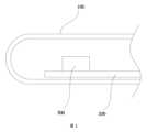
本出願の実施形態で提供されるパッケージングモジュールは、携帯電話やスマートウォッチなどの電子デバイスに適用される。図1は、電子デバイスに適用されたパッケージングモジュールの構造体の概略図である。電子デバイスは、ハウジング100と、ハウジング100内に配置されたメインボード200とを含む。パッケージングモジュール300は、メインボード200上に固定され、メインボード200に導電的に接続されている。 The packaging module provided in the embodiment of the present application is applied to electronic devices such as mobile phones and smart watches. Figure 1 isa schematic diagram of a structure of the packaging moduleapplied to an electronic device. The electronic device includes a
従来のシステムレベルのパッケージングモジュールが図2に示されている。パッケージングモジュールは、積層された第1の基板1と第2の基板2とを含み、第1の基板1と第2の基板2は、はんだボールを使用することによって接続されている。第1の基板1はチップ6を保持し、チップ6は、はんだボールを使用することによって第1の基板1に接続されており、第1の基板1と第2の基板2との間に位置する。第2の基板2は、積層されたチップ3およびチップ4と、チップ3およびチップ4をパッケージ化するパッケージング層5とを保持する。チップ3およびチップ4は、ポジティブマウント式に配置されている。具体的には、チップ3の接続面とチップ4の接続面は、チップの上面(チップの第2の基板2から離れた方に面する表面)に位置する。本出願のこの実施形態では、チップの接続面とは、チップに、別のチップまたは回路層への導電接続に使用されるはんだパッドまたは窓が設けられた表面を指す。チップ3およびチップ4が第2の基板2に接続される場合、チップ3の接続面およびチップ4の接続面は、ボンディングワイヤ7を使用することによって別々に第2の基板2に接続される。図2から、従来技術におけるパッケージングモジュールは、少なくとも2枚の基板(第1の基板1および第2の基板2)を含み、ボンディングワイヤ7の高さが、パッケージングモジュールの高さ方向に沿って確保される必要があることが分かる。電子デバイスの小型化の進展に伴い、電子デバイスの内部空間も徐々に縮小される。その結果、従来技術におけるパッケージングモジュールは、小型化された電子デバイスに適用できなくなり、電子デバイスのさらなる小型化を制限する主要因となる。したがって、本出願の一実施形態は、パッケージングモジュール内のチップの組み合わせ方を改善することによってパッケージングモジュールをさらに小型化するための、パッケージングモジュールを提供する。以下は、特定の添付の図面を参照して、本出願の実施形態で提供されるパッケージングモジュールを詳細に説明する。 A conventional system-level packaging module is shown in FIG. 2. The packaging module includes astacked first substrate 1 and a second substrate 2, which are connected by using solder balls. The first substrate 1 holds a chip 6, which is connected to the first substrate 1 by using solder balls and is located between the first substrate 1 and the second substrate 2. The second substrate 2 holds stacked
本出願の実施形態で提供されるパッケージングモジュールは、システムレベルのパッケージングモジュールであり、システムレベルのパッケージングモジュールは、CPU(中央処理装置)、SOC(システム・オン・チップ)、DRAM(ダイナミックランダムアクセスメモリ)、およびNAND(NANDフラッシュメモリ)などの異なる機能を有するチップを含む場合がある。 The packaging module provided in the embodiment of the present application is a system-level packaging module, which may include chips with different functions, such as a CPU(Central Processing Unit), a SOC(System on Chip), a DRAM(Dynamic Random Access Memory), and a NAND (NAND flash memory ).
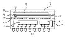
図3は、本出願の一実施形態によるパッケージングモジュールの断面の概略図である。パッケージングモジュールは、基板層10と複数のチップ層とを含み、パッケージングモジュールの層構造体は、説明を容易にするために命名されている。パッケージングモジュールの複数のチップ層は、最上チップ層30および最下チップ層20を含む。最上チップ層30は、複数のチップ層の中で基板層10から最も遠いチップ層であり、最下チップ層20は、複数のチップ層の中で基板層10から最も近いチップ層である。図3に示される構造体では、基板層10、最下チップ層20、および最上チップ層30は、垂直方向に積層されている(垂直方向は、パッケージングモジュールの厚さ方向と呼ばれてもよく、パッケージングモジュールの厚さ方向は、基板層10の厚さ方向と同じである)。最下チップ層20は、最上チップ層30の隣接チップ層である。加えて、最下チップ層20は、最上チップ層30よりも基板層10に近い。 FIG. 3 isa schematic diagram of a cross section of a packaging module according to an embodiment of the present application. The packaging module includes a
基板層10は、最上チップ層30および最下チップ層20を保持するための構造体として機能する。加えて、基板層10は、外部回路と最上チップ層30および最下チップ層20のチップとの間の導電接続を実現するためにさらに使用される。例えば、回路層が基板層10の表面上と基板層10の内部とに別々に配置され、基板層10の表面上の回路層と基板層10の内部の回路層とが、ビアを使用することによって電気的に接続されてもよい。The
任意選択の解決策では、基板層10内に埋め込みチップが配置され、埋め込みチップは、ビアまたは第1の導体aを使用することによって、基板層10の表面上の回路層または基板層10内に埋め込まれた回路層に電気的に接続される。図3は、2つの埋め込みチップ、第1の埋め込みチップ11および第2の埋め込みチップ12を示している。第1の埋め込みチップ11および第2の埋め込みチップ12は、ビアを使用することによって基板層10の回路層に導電的に接続されている。図3には2つの埋め込みチップが示されているが、埋め込みチップの数は、本出願のこの実施形態で提供されるパッケージングモジュールでは特に限定されず、埋め込みチップの数は1つ、3つなどであってもよいことを理解されたい。In an optional solution, an embedded chip is disposed in the
任意選択の解決策では、基板層10は、プリント回路基板であっても、別のタイプの回路基板であってもよい。In an optional solution, the
最下チップ層20は、同じ層に配置されたチップによって形成された層構造体である。例えば、最下チップ層20のチップは1つまたは複数のチップを含む。1つまたは複数のチップは、最上チップ層の第1のチップ31に接続するために使用されるチップである。図3に示されるように、例えば、最下チップ層20は、第2のチップ21および第3のチップ22を含む。最下チップ層20のチップが配置されている場合、1つまたは複数のチップの1つまたは複数の接続面は、基板層10に面するか、またはすべて基板層10に面し、基板層10の回路層に導電的に接続されている。例えば、第2のチップ21の接続面は基板層10に面し、はんだボールを使用することによって基板層10の回路層に導電的に接続されている。第3のチップ22の接続面は基板層10に面し、第3のチップ22の接続面は、基板層10の回路層に導電的に接続されている。組み立て中に、第2のチップ21の接続面は、はんだボールを使用することによって基板層10の回路層に導電的に接続され、第3のチップ22の接続面は、はんだボールを使用することによって基板層10の回路層に導電的に接続される。第2のチップ21および第3のチップ22は、基板層10の回路層を使用することによって、埋め込みチップ(第1の埋め込みチップまたは第2の埋め込みチップ)に電気的に接続されてもよい。The
本出願のこの実施形態で提供されるパッケージングモジュールは、最下チップ層20のチップの数を制限せず、異なる数のチップが必要に応じて配置されてもよいことを理解されたい。例えば、最下チップ層20のチップの数は、1つ、2つ、または3つである。 It should be understood that the packaging module provided in this embodiment of the present application does not limit the number of chips in the
最上チップ層30は、同じ層に配置されたチップによって形成された層構造体である。最上チップ層30は第1のチップ31を含む。図3では、例えば、最上チップ層30は1つの第1のチップ31を含む。第1のチップ31、第2のチップ21、および第3のチップ22は、積層されている。第1のチップ31の接続面は基板層10に面し、第1のチップ31の接続面は、第1の導体aを使用することによって第2のチップ21の接続面に導電的に接続されている。具体的には、第1の導体aの一端は第1のチップ31の接続面に接続されており、第1の導体aの他端は隣接チップ層のチップ(第2のチップ21)の接続面に接続されている。例えば、第1の導体aは、ボンディングワイヤであってもよいし、別の種類の導線であってもよい。 The
さらに図3を参照すると、配置されているとき、第1の導体aは、第1のチップ31の基板層10に面する側に配置されており、第1の導体aの最高点は、第1のチップ31の上面(基板層10から離れた方に面する表面)よりも低い。 Further referring to FIG. 3, when placed, the first conductor a is placed on the side of the
第1のチップ31が第2のチップ21に接続されるとき、第1のチップ31の接続面は、接着剤を使用することによって、第2のチップ21の、接続面から離れた方に面する上面と、第3のチップ22の、接続面から離れた方に面する上面とに別々に接合される。第1のチップ31の接続面には、第2のチップ21および第3のチップ22に対して露出した接続領域311が設けられている。第1の導体aの一端は、接続領域311に接続されている。図3に示されるように、例えば、接続領域311は、第1のチップ31の接続面の縁部領域に位置する。したがって、第1の導体aの配置が容易になる。 When the
本出願のこの実施形態で提供されるパッケージングモジュールは、パッケージング層40をさらに含む。パッケージング層40は、最下チップ層20、最上チップ層30、最下チップ層20と最上チップ層30との間の第1の導体a、および最下チップ層20を基板層10に接続するために使用されるはんだボールを包んで、パッケージングモジュール内のチップなどの構成部品を保護する。 The packaging module provided in this embodiment of the present application further includes a
本出願のこの実施形態で提供されるパッケージングモジュールの理解を容易にするために、以下は、パッケージングモジュールの作製ステップを詳細に説明する。To facilitate understanding of the packaging module provided in this embodiment of the present application, the following provides a detailed description of the fabrication steps of the packaging module.
ステップ1:第1のチップ31を保持プレート400に取り付ける。Step 1: Attach the
図4aを参照すると、保持プレート400は、金属、ガラス、またはシリコンなどの材料を使用することによって作製されてもよい。保持プレート400は、フィルム接着材料の層で覆われ、この材料の層は、第1のチップ31を固定するために使用される。フィルム接着材料は、感光性材料または感熱性材料であってもよい。紫外線によって照射されるか、または特定の加熱条件下に置かれた後、材料の接着力は大幅に低減されて、後の界面分離操作が容易になる。第1のチップ31が保持プレート400に固定されるとき、第1のチップ31の接続面は保持プレート400から離れた方に面する。第1のチップ31の厚さ範囲は、25μm~400μmであってもよい。例えば、第1のチップ31の厚さは、25μm、50μm、80μm、または400μmであってもよい。 Referring to FIG. 4a, the holding
ステップ2:第3のチップ22および第2のチップ21を第1のチップ31に取り付ける。Step 2: Attach the
図4bを参照すると、第3のチップ22の最下部および第2のチップ21の最下部で接着材料が提供され、第1のチップ31上に第3のチップ22および第2のチップ21を接合し、固定するために使用される。第3のチップ22の表面および第2のチップ21の表面には各々、基板層の回路層に接続される、はんだパッド構造体(図示せず)が設けられている。第3のチップ22および第2のチップ21が第1のチップ31に固定されるとき、第3のチップ22のはんだパッド(接続面上の構造体)および第2のチップ21のはんだパッドは、第1のチップ31から離れた方に面する。第2のチップ21、第3のチップ22、および第1のチップ31は、積層チップを形成する。 Referring to FIG. 4b, an adhesive material is provided at the bottom of the
第3のチップ22および第2のチップ21と第1のチップ31との間の接合に使用される接合材料は、特定の温度または紫外線環境で硬化されてもよい。第1のチップ31の厚さは、第2のチップ21の厚さと同じに設定される。例えば、第3のチップ22および第2のチップ21の各々の厚さ範囲は、25μm~400μmである。例えば、第2のチップ21の厚さおよび第3のチップ22の厚さは、各々、25μm、50μm、80μm、または400μmである。 The bonding material used for bonding between the
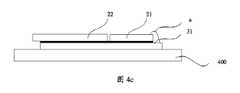
ステップ3:ボンディングワイヤを使用することによって第1のチップ31と第2のチップ21とを接続する。Step 3: Connect the
図4cを参照すると、第1のチップ31の接続面および第2のチップ21のはんだパッドに対してボンディングワイヤ接続を実施するために、ワイヤボンディングプロセスが使用される。ワイヤボンディングとは、熱、圧力、および超音波エネルギーにより、微細なボンディングワイヤを使用することによって、金属リード線と基板はんだパッドとを強固に溶接することを指す。前述のボンディングワイヤとして金、銅、または合金のボンディングワイヤが使用されてもよく、ボンディングワイヤの直径は、18μm~30μmであってもよい。例えば、ボンディングワイヤの直径は、18μm、25μm、または30μmである。 Referring to FIG. 4c, a wire bonding process is used to perform bonding wire connections to the connection surface of the
ステップ4:保持プレート400から積層チップを取り外し、積層チップを上下逆さまに置く。Step 4: Remove the stacked chip from the holding
図4dを参照すると、保持プレート400上のフィルム接着材料の接着力は、紫外線や加熱により大幅に低減され、次いで、第2のチップ21および第2のチップ21の上面は真空ゴム吸着ノズルによって吸着される。真空ゴム吸着ノズルは、第1のチップ31を保持プレート400から分離するために引き上げ装置によって上昇駆動され、積層チップ構造体は、仮の保持台500上に上下逆さまに置かれる。 4d, the adhesive force of the film adhesive material on the holding
ステップ5:基板層10を製造し、基板層10の表面上に金属バンプ13を打ち込む。Step 5: Manufacture the
図4eを参照すると、基板層10は、ファンアウト成形技術またはパネルレベルパッケージ技術を使用することによって実装される。基板層10は、第1の埋め込みチップ11および第2の埋め込みチップ12を埋め込まれ、第1の埋め込みチップ11および第2の埋め込みチップ12は、第1の埋め込みチップ11の接続端部および第2の埋め込みチップ12の接続端部をファンアウトするために、それぞれ回路層およびビアを使用することによって基板層10の表面上に再配線構造体を実装する。基板層10の表面上の回路層ははんだパッド構造体を含み、金属バンプ13は、メインボードまたは別の回路構造体に接続するために、はんだパッド構造体に打ち込まれる。基板層10の表面上の回路層は銅材料から作られてもよく、はんだパッド構造体の材料は銅を使用してもよく、はんだパッド上のバンプの材料は銅またはスズを使用してもよい。 Referring to FIG. 4e, the
金属バンプ13が基板層10上に作製されるとき、金属バンプ13は、印刷または電気めっきによってはんだパッド構造体に打ち込まれる。金属バンプ13の高さは、20μm~70μmであってもよい。例えば、金属バンプ13の高さは、20μm、40μm、または70μmである。 When the metal bumps 13 are fabricated on the
ステップ6:金属バンプを使用することによって積層チップ構造体を基板層10と接合する。 Step 6: Bond the stacked chip structure with the
図4fを参照すると、積層チップ構造体と基板層10とが合わせて置かれ、これにより金属バンプは、第3のチップ22に対応するパッドおよび第2のチップ21に対応するパッドと位置合わせされる。金属バンプは、リフローはんだ付けプロセスまたは熱圧入プロセスにより、第3のチップ22上のパッドおよび第2のチップ21上のパッドと金属接合される。前述の作製プロセスでは、リフローはんだ付けプロセスおよび熱圧入プロセスにより温度が上昇して、はんだを溶融させ、はんだを金属バンプの材料と溶融接合する。Referring to FIG. 4f, the stacked chip structure and the
ステップ7:パッケージング構造体全体を塑性的にパッケージ化し、はんだボールを基板層10に打ち込む。Step 7: The entire packaging structure is plastically packaged and the solder balls are hammered into the
図4gを参照すると、成形ツールおよび熱硬化性材料を使用することによってチップ構造体全体がパッケージ化されてもよく、パッケージング層40を形成するためにパッケージング材料が加熱によって硬化される。最後に、はんだボールが基板層10の下面に打ち込まれ、はんだボールは、はんだ印刷およびリフローはんだ付けによって打ち込まれてもよい。 4g, the entire chip structure may be packaged by using a molding tool and a thermosetting material, and the packaging material is cured by heating to form a
前述の説明から、本出願のこの実施形態で提供されるパッケージングモジュールでは、第1のチップ31が反転される(第1のチップ31の接続面が基板層10に面する)ので、第1のチップ31を第2のチップ21に接続するための第1の導体aの高さ値は、第2のチップ21の厚さ範囲内にありうることになり、追加の高さは必要とされないことが分かる。したがって、パッケージングモジュールはより薄くすることができる。 From the above description, it can be seen that in the packaging module provided in this embodiment of the present application, the
本出願のこの実施形態で提供されるパッケージングモジュールの薄型化効果の理解を容易にするために、本出願のこの実施形態で提供されるパッケージングモジュールは、図2に示される従来技術におけるパッケージングモジュールと比較される。To facilitate understanding of the thinning effect of the packaging module provided in this embodiment of the present application, the packaging module provided in this embodiment of the present application is compared with a packaging module in the prior art shown in FIG. 2.
本出願のこの実施形態では、図2に示されるチップはポジティブマウント式に配置され、チップ(チップ3およびチップ4)の接続面は、基板層から離れた方に面する。したがって、チップが第2の基板に接続されるとき、ボンディングワイヤはチップ4の最上部から引き出される必要がある。ボンディングワイヤが配線されるとき、必要な曲げラジアンが確保される必要があり、ボンディングワイヤを覆うために、パッケージング層5から最上部チップ(チップ4)までの厚さが少なくとも100μmに達する必要がある。しかしながら、本出願のこの実施形態で提供されるパッケージングモジュールでは、第1のチップの接続面が基板層に面するので、ボンディングワイヤは基板層に向かって配置される。ボンディングワイヤが最下チップ層のチップに接続されるときに曲げラジアンが確保される必要があるが、ボンディングワイヤの曲げによって占有される空間は、最下チップ層と基板層とを溶接するために使用されるはんだボールの空間と重複するので、追加の空間は必要とされない。本出願の図3から、チップ積層方向に沿ったボンディングワイヤの最高点(第1のチップの接続面に接続された点)が、第1のチップの上面よりも低く、パッケージング層から第1のチップの上面までの厚さに対する制限を効果的に低減することが分かる。したがって、パッケージングモジュールはより薄くすることができ、パッケージングモジュールのサイズは最小化される。 In this embodiment of the present application, the chips shown in FIG. 2 are arranged in a positive mount manner, and the connection surfaces of the chips (
加えて、従来技術におけるシステムレベルのパッケージングモジュールは、2枚の基板(第1の基板1および第2の基板2)を含むので、パッケージングモジュールのパッケージング厚さが増加する。しかしながら、本出願のこの実施形態では、一部のチップ(第1の埋め込みチップ11および第2の埋め込みチップ12)は埋め込み式に配置され、他のチップ(第1のチップ31、第2のチップ21、および第3のチップ22)は基板層10と直接接合される。これは、図2に示されるシステムレベルのパッケージングモジュールと比較して1つの基板構成部品の厚さを節減し、パッケージングモジュールの全体の厚さを低減する。加えて、チップと基板層との直接接合方式を使用することによって、従来のシステムレベルのパッケージングモジュールと比較してより多くのI/O(入力/出力)接続が実現されて、システムレベルのパッケージングモジュールのチップ間の接続帯域幅を増加させるか、または電力消費を削減することができる。 In addition, the system-level packaging module in the prior art includes two substrates (the first substrate 1 and the second substrate 2), which increases the packaging thickness of the packaging module.However, in this embodiment of the present application, some chips (the first embedded
前述の説明から、従来技術におけるパッケージングモジュールと比較して、本出願のこの実施形態で開示されるパッケージングモジュールは、パッケージング占有高さを大幅に低減することができることが分かる。例えば、従来技術では、携帯電話のプロセッサチップの積層パッケージングモジュールにおけるパッケージング層の占有高さは約1.2mmであり、スマートウォッチのプロセッサの積層パッケージングモジュールにおけるパッケージング層の占有高さは約0.8mmである。しかしながら、本出願のこの実施形態で提供されるパッケージングモジュールにおけるパッケージング層の厚さは、わずかに約0.5mmである。加えて、パッケージングモジュールが2枚の基板を使用する従来技術における解決策と比較して、本出願のこの実施形態で提供されるパッケージングモジュールでは、チップが基板層に直接接続される場合、パッケージングモジュールの内部のチップのI/O相互接続の数が増加されることができる。例えば、従来技術では、積層パッケージングモジュール内のCPUと上層DRAMパッケージングとの間のI/O接続の数は約200であり、本出願のこの実施形態で提供される基板層の、埋め込みチップと上層チップとの間のI/O接続の数は500よりも大きい。これは、I/O接続の数を大幅に増加させ、接続帯域幅をさらに増加させるか、または消費電力を削減する。 From the above description, it can be seen that compared with the packaging module in the prior art, the packaging module disclosed in this embodiment of the present applicationcan greatly reduce the packaging occupation height. For example, in the prior art, the occupation height of the packaging layer in the stacked packaging moduleofthe processor chip of the mobile phone is about 1.2 mm, and the occupation height of the packaging layer in the stacked packaging moduleof the processor of the smart watch is about 0.8 mm. However, the thickness of the packaging layer in the packaging module provided in this embodiment of the present application is only about 0.5 mm. In addition, compared with the solution in the prior art in which the packaging module uses two substrates, in the packaging module provided in this embodiment of the present application, the number of I/O interconnections of the chip inside the packaging modulecan be increased when the chip is directly connected to the substrate layer. For example, in the prior art, the number of I/Oconnections between the CPU and the upper layer DRAM packaging in the stacked packaging module is about 200, and the number of I/O connections between the embedded chip and the upper layer chip in the substrate layer provided in this embodiment of the present application is greater than 500. This allows for a significant increase in the number of I/Oconnections , further increasing connection bandwidth or reducing power consumption.
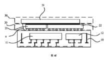
図5は、図3に示されるパッケージングモジュールに基づく変形構造体を示している。第2のチップ21および第3のチップ22は最下チップ層20に位置し、第1のチップ31は最上チップ層30に位置する。第2のチップ21および第3のチップ22と基板層10との接続方式については、図3の関連説明を参照されたい。ここでは詳細は再度説明されない。Figure 5 shows a modified structure based on the packaging module shown in Figure 3. The
基板層10には、ボンディングワイヤを回避するための回避溝14が設けられてもよく、回避溝14は、基板層10の第2のチップに面する表面に位置する。回避溝14の配置位置、幅、深さは、第1のチップ31および第2のチップ21に接続されたボンディングワイヤaの曲げ構造体の位置およびサイズに基づいて合致されてもよい。これは、本出願のこの実施形態において特に限定されない。The
加えて、回避溝14の数も、本出願のこの実施形態では特に限定されず、その数はボンディングワイヤaの数と合致してもよいし、または回避溝14の数はボンディングワイヤaの数よりも少ない。構成時には、1つの回避溝14が1つのボンディングワイヤaの曲げ構造体を収容してもよいし、または1つの回避溝14は、複数のボンディングワイヤaの曲げ構造体を収容する。特定の配置時に、回避溝14の位置および回避溝14の数は、配置された回避溝14が回路層の金属配線に影響を及ぼすのを防ぐために、基板層10の表面上の回路層の金属配線に基づいて柔軟に構成されてもよい。In addition, the number of avoidance grooves 14 is also not particularly limited in this embodiment of the present application, and the number may match the number of bonding wires a, or the number of avoidance grooves 14 is less than the number of bonding wires a. When configured, one avoidance groove 14 may accommodate the bending structure of one bonding wire a, or one avoidance groove 14 accommodates the bending structures of multiple bonding wires a. When specifically arranged, the position of the avoidance groove 14 and the number of avoidance grooves 14 may be flexibly configured based on the metal wiring of the circuit layer on the surface of the
図5から、回避溝14が配置される場合、パッケージングモジュールのサイズがさらに縮小されることができるので、第2のチップ21および第3のチップ22を基板層10に接続するはんだボールは、パッケージングモジュールの高さをさらに低減するために、より小さいサイズを有することができることが分かる。加えて、回避溝14が配置されているので、ボンディングワイヤは曲げのためのより大きい空間を有する。これは、曲げ加工後のボンディングワイヤの信頼性を確実にする。 It can be seen from Fig. 5 that when the avoidance groove 14 is arranged, the size of the packaging modulecan be further reduced, so that the solder balls connecting the
図6は、図3に示されるパッケージングモジュールに基づく別の変形構造体を示している。第2のチップ21および第3のチップ22は最下チップ層20に位置し、第1のチップ31は最上チップ層30に位置する。第2のチップ21および第3のチップ22と基板層10との接続方式については、図3の関連説明を参照されたい。ここでは詳細は再度説明されない。Figure 6 shows another modified structure based on the packaging module shown in Figure 3. The
図6に示されるパッケージング構造体では、パッケージングモジュールの第2のチップ21および第3のチップ22は、第1のチップ31の中央領域に別々に接続されている。図6から分かるように、第1のチップ31の接続領域311は、第1のチップ31の接続面の中央領域に位置し、第2のチップ21と第3のチップ22とは間隔を置いて配置されており、接続領域311を露出させるための空間が、第2のチップ21と第3のチップ22との間に間隔を置いて配置されている。第1のチップ31が第2のチップ21および第3のチップ22に接続される場合、第1のチップ31は、1つの第1の導体を使用することによって第2のチップ21に導電的に接続され、第1のチップ31は、別の第1の導体を使用することによって第3のチップ22に導電的に接続される。In the packaging structure shown in FIG. 6, the
第1の導体は、ボンディングワイヤを使用する。例えば、第2のチップ21と第3のチップ22との間の間隙にボンディングワイヤbおよびボンディングワイヤcが位置する。図6に示されるパッケージング構造体が使用される場合、ボンディングワイヤbおよびボンディングワイヤcを収容するための空間が、第1のチップ31のサイズと、第2のチップ21のサイズと、第3のチップ22のサイズとの差を利用することによって、第2のチップ21と第3のチップ22との間に形成される。したがって、ボンディングワイヤbおよびボンディングワイヤcは、パッケージングモジュールの水平方向(図6に示される方向B)のサイズに影響を及ぼさない。これは、パッケージングモジュールのサイズをさらに縮小し、パッケージングモジュールの小型化を容易にする。The first conductor uses a bonding wire. For example, the bonding wire b and the bonding wire c are located in the gap between the
加えて、図6に示されるパッケージングモジュールは、図5に示される回避溝も使用してもよい。具体的には、パッケージングモジュールの高さをさらに低減するために、図6に示されるパッケージングモジュールの基板層10上に、ボンディングワイヤbおよびボンディングワイヤcと合致する回避溝も配置されてもよい。 In addition, the packaging module shown in Fig. 6 may also use the avoidance groove shown in Fig. 5. Specifically, to further reduce the height of the packaging module, an avoidance groove that matches the bonding wireb and the bonding wirec may also be disposed on the
図7は、図3に示されるパッケージングモジュールに基づく変形例によって得られたパッケージングモジュールを示している。図7の一部の参照符号については、図3の同じ参照符号を参照されたい。第4のチップ23および第5のチップ24が最下チップ層20に位置し、第1のチップ31は最上チップ層30に位置する。Figure 7 shows a packaging module obtained by a modified example based on the packaging module shown in Figure 3. For some reference numbers in Figure 7, please refer to the same reference numbers in Figure 3. The
図7に示されるパッケージングモジュールでは、最下チップ層20の一部のチップの引き出し面が基板層10に面している。図7に示されるように、第4のチップ23の引き出し面は、基板層10に面している。第4のチップ23と基板層10との接続方式については、図3の第2のチップ21および基板層10の関連説明を参照されたい。ここでは詳細は再度説明されない。第5のチップ24が配置される場合、第5のチップ24は基板層10と接合され、第5のチップ24の接続面は基板層10から離れた方に面する。第5のチップ24の接続面は、第2の導体を使用することによって基板層10の回路層に導電的に接続されている。例えば、第2の導体は、ボンディングワイヤdを使用してもよい。 In the packaging module shown in FIG. 7, the lead-out surface of some chips in the
第1のチップ31および第5のチップ24が配置される場合、第5のチップ24と第1のチップ31とは互い違いに配置されるので、第5のチップ24の接続面は第1のチップ31の外側に露出し、ボンディングワイヤdは、第1のチップ31の外側に露出した第5のチップ24の接続面の一部に接続される。When the
任意選択の解決策では、ボンディングワイヤdの高さは、配置されたボンディングワイヤdがパッケージングモジュールの高さに影響を及ぼすのを防ぐために、基板層10から離れた方に面する第1のチップ31の表面の高さよりも低い。In an optional solution, the height of the bonding wire d is less than the height of the surface of the
図8は、図3に示されるパッケージングモジュールに基づく別の変形構造体を示している。図8の一部の参照符号については、図3の同じ参照符号を参照されたい。複数のチップ層は、最上チップ層30、中間チップ層50、および最下チップ層20を含む。最下チップ層20は、基板層に最も近いチップ層である。中間チップ層50は、最下チップ層20と最上チップ層30との間に位置するチップ層であり、中間チップ層50は、最上チップ層30に隣接するチップ層である。最上チップ層30は第1のチップ31を含み、中間チップ層は第6のチップ51を含む。第6のチップ51の接続面は基板層10に面し、最下チップ層20は、第7のチップ25および第10のチップ26を含む。第7のチップ25の接続面および第10のチップ26の接続面は、基板層10に面し、基板層10の回路層に導電的に接続されている。 FIG. 8 shows another modified structure based on the packaging module shown in FIG. 3. Some reference numbers in FIG. 8 should be referred to the same reference numbers in FIG. 3. The multiple chip layers include a
最下チップ層20の第7のチップ25および第10のチップ26と基板層10との接続方式については、図3に示される第2のチップ21および第3のチップ22と基板層10との接続方式を参照されたい。ここでは詳細は再度説明されない。For the connection method between the
第6のチップ51の接続面は、第1の導体を使用することによって、第1のチップ31の接続面と第7のチップ25の接続面とに別々に導電的に接続されている。図8に示されるように、第1の導体は、ボンディングワイヤeおよびボンディングワイヤfである。第1のチップ31と第6のチップ51とは、ボンディングワイヤeを使用することによって接続されており、第6のチップ51と第7のチップ25とは、ボンディングワイヤfを使用することによって接続されている。具体的な接続方式については、第1のチップ31と第2のチップ21とが図3のボンディングワイヤaを使用することによって接続される方式を参照されたい。ここでは詳細は再度説明されない。 The connection surface of the
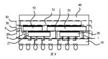
図9は、図3に示されるパッケージングモジュールに基づく別の変形構造体を示している。図9に示される構造体では、図3に示される基板層10の埋め込みチップが基板層の表面に配置されているものと理解されよう。Figure 9 shows another modified structure based on the packaging module shown in Figure 3. It will be understood that in the structure shown in Figure 9, the embedded chip of the
図9では、複数のチップ層は、最上チップ層30、中間チップ層50、および最下チップ層20を含む。最下チップ層20は、基板層に最も近いチップ層である。中間チップ層50は、最下チップ層20と最上チップ層30との間に位置するチップ層であり、中間チップ層50は、最上チップ層20に隣接するチップ層である。最下チップ層20は第9のチップ27および第11のチップ28を含み、中間チップ層50は第8のチップ52および第12のチップ53を含み、最上チップ層30は第1のチップ31を含む。In FIG. 9, the multiple chip layers include a
最下チップ層20の第9のチップ27および第11のチップ28と基板層10との接続方式については、図3に示される第2のチップ21および第3のチップ22と基板層10との接続方式を参照されたい。ここでは詳細は再度説明されない。For the connection method between the
第9のチップ27の接続面および第11のチップ28の接続面は両方とも基板層10に面している。第9のチップ27および第11のチップ28は、はんだパッドを使用することによって基板層10の回路層に導電的に接続されている。加えて、第9のチップ27および第11のチップ28は、別のチップと基板層10の回路層との間の導電接続のための配線空間を確保するために、間隔を置いて配置されている。The connection surface of the
中間チップ層50の第8のチップ52と第9のチップ27は、接着剤によって接合されている。第8のチップ52と第9のチップ27とは互い違いに配置されているので、第8のチップ52は、第9のチップ27の外部に部分的に露出している。第8のチップ52の接続面は基板層10に面し、第9のチップ27の外部に露出した第8のチップ52の接続面の一部は、導電柱hを使用することによって基板層10の回路層に導電的に接続されている。第12のチップ53は、接着剤によって第9のチップ27および第11のチップ28と接合されている。第12のチップ53と第11のチップ28とは互い違いに配置されているので、第12のチップ53は、第11のチップ28の外部に部分的に露出している。第12のチップ53の接続面は基板層10に面し、第9のチップ27および第11のチップ28の外部に露出した第12のチップ53の接続面の一部は、導電柱(第3の導体)使用することによって、基板層10の回路層に導電的に接続されている。図9に示されるように、第12のチップ53は、導電柱jおよび導電柱iを別々に使用することによって、基板層10の回路層に導電的に接続されている。図9に示される第12のチップ53と基板層10の回路層との導電接続方式は、単なる特定の方式例にすぎないことを理解されたい。実際の製造において、配線設計は、チップの特定の位置に基づいて実装されてもよい。 The
最上チップ層30は第1のチップ31を含み、第1のチップ31は、接着剤によって、第8のチップ52および第12のチップ53と別々に接合されている。加えて、第1のチップ31と第8のチップ52とは互い違いに配置されているので、第1のチップ31は、第8のチップ52の外側に部分的に露出している。第1のチップ31の接続面は基板層10に面し、第8のチップ52の外部に露出した第1のチップ31の接続面の一部は、ボンディングワイヤg(第1の導体)を使用することによって、第8のチップ52の接続面に導電的に接続されている。 The
前述の例は、異なるチップ層が1つまたは2つのチップを含むことを示しているが、本出願のこの実施形態では、各チップ層のチップの数は特に限定されず、異なる数のチップが実際の状況に基づいて選択されてもよいことを理解されたい。Although the above examples show that different chip layers include one or two chips, it should be understood that in this embodiment of the present application, the number of chips in each chip layer is not particularly limited, and different numbers of chips may be selected based on actual circumstances.
図9に示されるパッケージングモジュールの構造体から、本出願のこの実施形態で提供されるパッケージングモジュールでは、最上層のチップが反転されるので、最上層のチップと別の層のチップとの間の導電接続のための導体がパッケージングモジュールの空間を占有しないことが分かる。パッケージングモジュールのサイズが縮小される。加えて、図9に示されるパッケージングモジュールは埋め込みチップを使用しないが、図9に示されるパッケージングモジュールは、図2に示されるパッケージングモジュールと比較して、使用される基板の数を低減する。これもまた、パッケージングモジュールのサイズを縮小させる。From the structure of the packaging module shown in FIG. 9, it can be seen that in the packaging module provided in this embodiment of the present application, the chip in the top layer is inverted, so that the conductor for the conductive connection between the chip in the top layer and the chip in another layer does not occupy the space of the packaging module. The size of the packaging module is reduced. In addition, although the packaging module shown in FIG. 9 does not use an embedded chip, the packaging module shown in FIG. 9 reduces the number of substrates used compared with the packaging module shown in FIG. 2. This also reduces the size of the packaging module.
本出願の一実施形態は、携帯電話やスマートウォッチなどの電子デバイスをさらに提供する。図1に示される電子デバイスの構造体が一例として使用される。電子デバイスは、ハウジング100と、ハウジング100内に配置されたメインボード200とを含む。パッケージングモジュール300は、メインボード200上に固定され、メインボード200に導電的に接続されている。パッケージングモジュール300が前述の例におけるパッケージングモジュールを使用する場合、使用される基板の数を低減し、パッケージングモジュールの厚さをさらに低減するために、すべてのチップが1枚の基板(基板層)によって支持される。加えて、第1のチップの接続面が基板層に面するので、第1のチップおよび別のチップに接続された第1の導体が追加の空間を占有せずに、パッケージングモジュールの厚さを低減し、パッケージングモジュールの小型化を容易にする。 An embodiment of the present application further provides an electronic device, such as a mobile phone or a smart watch. The structure of the electronic device shown in FIG. 1 is used as an example. The electronic device includes a
明らかに、当業者は、本出願の範囲から逸脱することなく、本出願に対して様々な修正および変形を行うことができる。本出願は、本出願のそれらの修正および変形が以下の特許請求の範囲およびその均等な技術によって規定される保護範囲内にあるならば、それらの修正および変形を包含することを意図されている。 Obviously, those skilled in the art can make various modifications and variations to this application without departing fromthe scope of this application. This application is intended to cover those modifications and variations of this application as long as they fall within the scope of protection defined by the following claims and their equivalent technologies.
1 第1の基板
2 第2の基板
3 チップ
4 チップ
5 パッケージング層
6 チップ
7 ボンディングワイヤ
10 基板層
11 第1の埋め込みチップ
12 第2の埋め込みチップ
13 金属バンプ
14 回避溝
20 最下チップ層
21 第2のチップ
22 第3のチップ
23 第4のチップ
24 第5のチップ
25 第7のチップ
26 第10のチップ
27 第9のチップ
28 第11のチップ
30 最上チップ層
31 第1のチップ
40 パッケージング層
50 中間チップ層
51 第6のチップ
52 第8のチップ
53 第12のチップ
100 ハウジング
200 メインプレート
300 パッケージングモジュール
311 接続領域
400 保持プレート
500 仮の保持プレート 1 First Substrate
2 Second Board
3. Chip
4 Chips
5 Packaging Layer
6. Chips
7 Bonding Wire
10 Substrate Layer
11 The first embedded chip
12 Second embedded chip
13 Metal bump
14 Avoidance Groove
20 Bottom Chip Layer
21 The second chip
22 The third chip
23 The Fourth Chip
24 The Fifth Chip
25 The Seventh Chip
26 The 10th Chip
27 The 9th Chip
28 The 11th Chip
30 Top Chip Layer
31 The First Chip
40 Packaging Layer
50 Middle chip layer
51 The Sixth Chip
52 The 8th Chip
53 The 12th Chip
100 Housing
200 Main Plate
300 Packaging Module
311 Connection Area
400 Retaining Plate
500 Temporary Retaining Plate
Claims (12)
Translated fromJapanese前記最上チップ層は第1のチップを含み、前記第1のチップの接続面は前記基板層に面し、前記第1のチップの前記接続面は、第1の導体を使用することによって、隣接チップ層のチップに導電的に接続されており、
前記基板層に、前記第1の導体を回避するための回避溝が設けられている、パッケージングモジュール。 A packaging module including a substrate layer and a plurality of chip layers stacked on the substrate layer, the plurality of chip layers including a top chip layer, the top chip layer being the chip layer furthest from the substrate layer;
the top chip layer includes a first chip, a connection side of the first chip facing the substrate layer, the connection side of the first chip conductively connected to a chip of an adjacent chip layer by using a first conductor;
A packaging module, wherein the substrate layer is provided with an avoidance groove for avoiding the first conductor .
前記第1のチップは、前記第1の導体を使用することによって前記第2のチップに導電的に接続されているか、または、
前記第1のチップは、1つの第1の導体を使用することによって前記第2のチップに導電的に接続されており、前記第1のチップは、別の第1の導体を使用することによって前記第3のチップに導電的に接続されている、請求項5に記載のパッケージングモジュール。 the adjacent chip layer includes a plurality of chips, the plurality of chips including a second chip and a third chip, a connection surface of the second chip and a connection surface of the third chip both facing the substrate layer, the second chip and the third chip being separately conductively connected to the circuit layer of the substrate layer;
the first chip is conductively connected to the second chip by using the first conductor; or
6. The packaging module of claim 5, wherein the first chip is conductively connected to the second chip by using one first conductor, and the first chip is conductively connected to the third chip by using another first conductor.
前記第5のチップの接続面は前記基板層から離れた方に面し、前記第5のチップの前記接続面は、第2の導体を使用することによって前記基板層の前記回路層に導電的に接続されている、請求項5に記載のパッケージングモジュール。 the adjacent chip layer includes a plurality of chips, the plurality of chips including a fourth chip and a fifth chip, a connection surface of the fourth chip facing the substrate layer, the connection surface of the first chip conductively connected to the connection surface of the fourth chip by using the first conductor;
6. The packaging module of claim 5, wherein a connection surface of the fifth chip faces away from the substrate layer, and the connection surface of the fifth chip is conductively connected to the circuit layer of the substrate layer by using a second conductor.
前記隣接チップ層に位置するチップは第6のチップを含み、前記第6のチップの接続面は前記基板層に面し、前記最下チップ層に位置するチップは第7のチップを含み、前記第7のチップの接続面は前記基板層に面し、前記基板層の回路層に導電的に接続されており、
前記第6のチップの前記接続面は、1つの第1の導体を使用することによって前記第1のチップの前記接続面に導電的に接続されており、別の第1の導体を使用することによって前記第7のチップの前記接続面に導電的に接続されている、請求項1から4のいずれか一項に記載のパッケージングモジュール。 the plurality of chip layers further includes a bottom chip layer, the bottom chip layer being the chip layer closest to the substrate layer, and the adjacent chip layer being located between the bottom chip layer and the top chip layer;
the chips located in the adjacent chip layer include a sixth chip, a connection surface of the sixth chip facing the substrate layer, the chips located in the bottom chip layer include a seventh chip, a connection surface of the seventh chip facing the substrate layer and conductively connected to a circuit layer of the substrate layer;
5. A packaging module according to claim 1, wherein the connection surface of the sixth chip is conductively connected to the connection surface of the first chip by using one first conductor and is conductively connected to the connection surface of the seventh chip by using another first conductor.
前記隣接チップ層に位置するチップは第8のチップを含み、前記第8のチップの接続面は前記基板層に面し、前記最下チップ層に位置するチップは第9のチップを含み、前記第9のチップの接続面は前記基板層に面し、前記基板層の回路層に導電的に接続されており、
前記第1のチップの前記接続面は、前記第1の導体を使用することによって前記第8のチップの前記接続面に導電的に接続されており、
前記第9のチップの前記接続面は、第3の導体を使用することによって前記基板層の前記回路層に導電的に接続されている、請求項1から4のいずれか一項に記載のパッケージングモジュール。 the plurality of chip layers further includes a bottom chip layer, the bottom chip layer being the chip layer closest to the substrate layer, and the adjacent chip layer being located between the bottom chip layer and the top chip layer;
the chips located in the adjacent chip layer include an eighth chip, a connection surface of the eighth chip facing the substrate layer, the chips located in the bottom chip layer include a ninth chip, a connection surface of the ninth chip facing the substrate layer and conductively connected to a circuit layer of the substrate layer;
the connection surface of the first chip is conductively connected to the connection surface of the eighth chip by using the first conductor;
5. The packaging module of claim 1, wherein the connection surface of the ninth chip is conductively connected to the circuit layer of the substrate layer by using a third conductor.
Applications Claiming Priority (3)
| Application Number | Priority Date | Filing Date | Title |
|---|---|---|---|
| CN202011380744.2ACN112614830A (en) | 2020-11-30 | 2020-11-30 | Encapsulation module and electronic equipment |
| CN202011380744.2 | 2020-11-30 | ||
| PCT/CN2021/097931WO2022110746A1 (en) | 2020-11-30 | 2021-06-02 | Packaging module, and electronic apparatus |
Publications (2)
| Publication Number | Publication Date |
|---|---|
| JP2023551331A JP2023551331A (en) | 2023-12-07 |
| JP7635383B2true JP7635383B2 (en) | 2025-02-25 |
Family
ID=75229801
Family Applications (1)
| Application Number | Title | Priority Date | Filing Date |
|---|---|---|---|
| JP2023532830AActiveJP7635383B2 (en) | 2020-11-30 | 2021-06-02 | Packaging module and electronic device |
Country Status (6)
| Country | Link |
|---|---|
| US (1) | US20230307428A1 (en) |
| EP (1) | EP4246578A4 (en) |
| JP (1) | JP7635383B2 (en) |
| KR (1) | KR102808830B1 (en) |
| CN (1) | CN112614830A (en) |
| WO (1) | WO2022110746A1 (en) |
Families Citing this family (1)
| Publication number | Priority date | Publication date | Assignee | Title |
|---|---|---|---|---|
| CN112614830A (en)* | 2020-11-30 | 2021-04-06 | 华为技术有限公司 | Encapsulation module and electronic equipment |
Citations (6)
| Publication number | Priority date | Publication date | Assignee | Title |
|---|---|---|---|---|
| JP2003031760A (en) | 2001-07-11 | 2003-01-31 | Nec Kyushu Ltd | Semiconductor device |
| JP2006294974A (en) | 2005-04-13 | 2006-10-26 | Denso Corp | Electronic equipment and its manufacturing method |
| US20080284003A1 (en) | 2007-05-17 | 2008-11-20 | Chua Swee Kwang | Semiconductor Packages And Method For Fabricating Semiconductor Packages With Discrete Components |
| US20090091042A1 (en) | 2007-10-04 | 2009-04-09 | Byung Tai Do | Integrated circuit package system including die having relieved active region |
| JP2014150265A (en) | 2014-03-10 | 2014-08-21 | Dainippon Printing Co Ltd | Wiring board for electronic module |
| US20170033087A1 (en) | 2015-07-31 | 2017-02-02 | Samsung Electronics Co., Ltd. | Stack semiconductor package structure and method of manufacturing the same |
Family Cites Families (17)
| Publication number | Priority date | Publication date | Assignee | Title |
|---|---|---|---|---|
| KR20070088177A (en)* | 2006-02-24 | 2007-08-29 | 삼성테크윈 주식회사 | Semiconductor package and manufacturing method thereof |
| JP2008270597A (en)* | 2007-04-23 | 2008-11-06 | Toshiba Corp | Semiconductor device |
| KR20100049283A (en)* | 2008-11-03 | 2010-05-12 | 삼성전자주식회사 | Semiconductor package and method for manufacturing of the same |
| US8236607B2 (en)* | 2009-06-19 | 2012-08-07 | Stats Chippac Ltd. | Integrated circuit packaging system with stacked integrated circuit and method of manufacture thereof |
| KR101686199B1 (en)* | 2010-03-26 | 2016-12-14 | 삼성전자주식회사 | Semiconductor Package Structure |
| TWI409933B (en)* | 2010-06-15 | 2013-09-21 | Powertech Technology Inc | Chip stacked package structure and its fabrication method |
| CN104392979A (en)* | 2014-11-17 | 2015-03-04 | 三星半导体(中国)研究开发有限公司 | Chip stacking encapsulation structure |
| US9633974B2 (en)* | 2015-03-04 | 2017-04-25 | Apple Inc. | System in package fan out stacking architecture and process flow |
| CN105006470A (en)* | 2015-07-31 | 2015-10-28 | 三星半导体(中国)研究开发有限公司 | A semiconductor stack package structure and manufacturing method thereof |
| CN105870024B (en)* | 2016-06-15 | 2018-07-27 | 通富微电子股份有限公司 | System-in-a-package method |
| CN206236120U (en)* | 2016-09-09 | 2017-06-09 | 深圳芯启航科技有限公司 | A kind of fingerprint recognition module |
| US11276667B2 (en)* | 2016-12-31 | 2022-03-15 | Intel Corporation | Heat removal between top and bottom die interface |
| CN110246812A (en)* | 2018-03-08 | 2019-09-17 | 恒劲科技股份有限公司 | A kind of semiconductor package and preparation method thereof |
| US10340249B1 (en)* | 2018-06-25 | 2019-07-02 | Taiwan Semiconductor Manufacturing Company, Ltd. | Semiconductor device and method |
| CN109585431A (en)* | 2018-12-17 | 2019-04-05 | 华进半导体封装先导技术研发中心有限公司 | A kind of fan-out packaging structure and its manufacturing method of Flash chip stacking |
| JP7455951B2 (en)* | 2019-11-29 | 2024-03-26 | 長江存儲科技有限責任公司 | Chip package structure and method for manufacturing chip package structure |
| CN112614830A (en)* | 2020-11-30 | 2021-04-06 | 华为技术有限公司 | Encapsulation module and electronic equipment |
- 2020
- 2020-11-30CNCN202011380744.2Apatent/CN112614830A/enactivePending
- 2021
- 2021-06-02JPJP2023532830Apatent/JP7635383B2/enactiveActive
- 2021-06-02WOPCT/CN2021/097931patent/WO2022110746A1/ennot_activeCeased
- 2021-06-02EPEP21896255.3Apatent/EP4246578A4/enactivePending
- 2021-06-02KRKR1020237022063Apatent/KR102808830B1/enactiveActive
- 2023
- 2023-05-30USUS18/325,306patent/US20230307428A1/enactivePending
Patent Citations (6)
| Publication number | Priority date | Publication date | Assignee | Title |
|---|---|---|---|---|
| JP2003031760A (en) | 2001-07-11 | 2003-01-31 | Nec Kyushu Ltd | Semiconductor device |
| JP2006294974A (en) | 2005-04-13 | 2006-10-26 | Denso Corp | Electronic equipment and its manufacturing method |
| US20080284003A1 (en) | 2007-05-17 | 2008-11-20 | Chua Swee Kwang | Semiconductor Packages And Method For Fabricating Semiconductor Packages With Discrete Components |
| US20090091042A1 (en) | 2007-10-04 | 2009-04-09 | Byung Tai Do | Integrated circuit package system including die having relieved active region |
| JP2014150265A (en) | 2014-03-10 | 2014-08-21 | Dainippon Printing Co Ltd | Wiring board for electronic module |
| US20170033087A1 (en) | 2015-07-31 | 2017-02-02 | Samsung Electronics Co., Ltd. | Stack semiconductor package structure and method of manufacturing the same |
Also Published As
| Publication number | Publication date |
|---|---|
| US20230307428A1 (en) | 2023-09-28 |
| JP2023551331A (en) | 2023-12-07 |
| CN112614830A (en) | 2021-04-06 |
| KR102808830B1 (en) | 2025-05-15 |
| WO2022110746A1 (en) | 2022-06-02 |
| EP4246578A4 (en) | 2024-07-17 |
| EP4246578A1 (en) | 2023-09-20 |
| KR20230111246A (en) | 2023-07-25 |
Similar Documents
| Publication | Publication Date | Title |
|---|---|---|
| US10555417B2 (en) | Mainboard assembly including a package overlying a die directly attached to the mainboard | |
| US10879219B2 (en) | Lower IC package structure for coupling with an upper IC package to form a package-on-package (PoP) assembly and PoP assembly including such a lower IC package structure | |
| US8664780B2 (en) | Semiconductor package having plural semiconductor chips and method of forming the same | |
| JP5205867B2 (en) | Semiconductor device and manufacturing method thereof | |
| US8026584B2 (en) | Semiconductor package, module, system having solder ball coupled to chip pad and manufacturing method thereof | |
| JP4149289B2 (en) | Semiconductor device | |
| US20090146283A1 (en) | Stacked-type chip package structure and fabrication method thereof | |
| KR20110128748A (en) | Integrated circuit packaging system with double side connections and manufacturing method thereof | |
| JP2002222889A (en) | Semiconductor device and method of manufacturing the same | |
| TWI536523B (en) | Integrated circuit packaging system with vertical interconnects and method of manufacture thereof | |
| KR20030018642A (en) | Stack chip module | |
| KR20120029169A (en) | Print circuit board having hexagonal bump pad for substrate of semiconductor package and semiconductor package having the same | |
| JP4930699B2 (en) | Semiconductor device | |
| JP2006295183A (en) | A multi-package module comprising a stacked package comprising a die and a mold body arranged asymmetrically. | |
| JP7635383B2 (en) | Packaging module and electronic device | |
| US20030015803A1 (en) | High-density multichip module and method for manufacturing the same | |
| TW200933868A (en) | Stacked chip package structure | |
| CN222462894U (en) | Flip chip packaging structure and electronic equipment | |
| CN221783207U (en) | Chip packaging structure and electronic equipment | |
| TW201343019A (en) | System in package assembly, print circuit board assembly and fabrications thereof | |
| CN117393534A (en) | Chip packaging structure and electronic equipment | |
| KR20080074654A (en) | Laminated Semiconductor Packages | |
| JP2001127241A (en) | Semiconductor multi-chip package, semiconductor device, electronic device, and manufacturing method thereof | |
| CN117712131A (en) | Semiconductor chip packaging structure and formation method thereof | |
| WO2025030593A1 (en) | Chip stacking heat dissipation structure, three-dimensional stacking packaging system and manufacturing method |
Legal Events
| Date | Code | Title | Description |
|---|---|---|---|
| A521 | Request for written amendment filed | Free format text:JAPANESE INTERMEDIATE CODE: A523 Effective date:20230711 | |
| A621 | Written request for application examination | Free format text:JAPANESE INTERMEDIATE CODE: A621 Effective date:20230711 | |
| A977 | Report on retrieval | Free format text:JAPANESE INTERMEDIATE CODE: A971007 Effective date:20240725 | |
| A131 | Notification of reasons for refusal | Free format text:JAPANESE INTERMEDIATE CODE: A131 Effective date:20240805 | |
| A521 | Request for written amendment filed | Free format text:JAPANESE INTERMEDIATE CODE: A523 Effective date:20241017 | |
| TRDD | Decision of grant or rejection written | ||
| A01 | Written decision to grant a patent or to grant a registration (utility model) | Free format text:JAPANESE INTERMEDIATE CODE: A01 Effective date:20250128 | |
| A61 | First payment of annual fees (during grant procedure) | Free format text:JAPANESE INTERMEDIATE CODE: A61 Effective date:20250212 | |
| R150 | Certificate of patent or registration of utility model | Ref document number:7635383 Country of ref document:JP Free format text:JAPANESE INTERMEDIATE CODE: R150 |