JP7633255B2 - Chamber Deposition and Etch Process - Google Patents
Chamber Deposition and Etch ProcessDownload PDFInfo
- Publication number
- JP7633255B2 JP7633255B2JP2022533217AJP2022533217AJP7633255B2JP 7633255 B2JP7633255 B2JP 7633255B2JP 2022533217 AJP2022533217 AJP 2022533217AJP 2022533217 AJP2022533217 AJP 2022533217AJP 7633255 B2JP7633255 B2JP 7633255B2
- Authority
- JP
- Japan
- Prior art keywords
- substrate
- substrate support
- faceplate
- semiconductor processing
- plasma
- Prior art date
- Legal status (The legal status is an assumption and is not a legal conclusion. Google has not performed a legal analysis and makes no representation as to the accuracy of the status listed.)
- Active
Links
Images


Classifications
- H—ELECTRICITY
- H01—ELECTRIC ELEMENTS
- H01L—SEMICONDUCTOR DEVICES NOT COVERED BY CLASS H10
- H01L21/00—Processes or apparatus adapted for the manufacture or treatment of semiconductor or solid state devices or of parts thereof
- H01L21/02—Manufacture or treatment of semiconductor devices or of parts thereof
- H01L21/027—Making masks on semiconductor bodies for further photolithographic processing not provided for in group H01L21/18 or H01L21/34
- H01L21/033—Making masks on semiconductor bodies for further photolithographic processing not provided for in group H01L21/18 or H01L21/34 comprising inorganic layers
- H01L21/0334—Making masks on semiconductor bodies for further photolithographic processing not provided for in group H01L21/18 or H01L21/34 comprising inorganic layers characterised by their size, orientation, disposition, behaviour, shape, in horizontal or vertical plane
- H01L21/0337—Making masks on semiconductor bodies for further photolithographic processing not provided for in group H01L21/18 or H01L21/34 comprising inorganic layers characterised by their size, orientation, disposition, behaviour, shape, in horizontal or vertical plane characterised by the process involved to create the mask, e.g. lift-off masks, sidewalls, or to modify the mask, e.g. pre-treatment, post-treatment
- H—ELECTRICITY
- H01—ELECTRIC ELEMENTS
- H01L—SEMICONDUCTOR DEVICES NOT COVERED BY CLASS H10
- H01L21/00—Processes or apparatus adapted for the manufacture or treatment of semiconductor or solid state devices or of parts thereof
- H01L21/02—Manufacture or treatment of semiconductor devices or of parts thereof
- H01L21/02041—Cleaning
- H01L21/02082—Cleaning product to be cleaned
- H01L21/02087—Cleaning of wafer edges
- H—ELECTRICITY
- H01—ELECTRIC ELEMENTS
- H01L—SEMICONDUCTOR DEVICES NOT COVERED BY CLASS H10
- H01L21/00—Processes or apparatus adapted for the manufacture or treatment of semiconductor or solid state devices or of parts thereof
- H01L21/02—Manufacture or treatment of semiconductor devices or of parts thereof
- H01L21/02104—Forming layers
- H01L21/02107—Forming insulating materials on a substrate
- H01L21/02109—Forming insulating materials on a substrate characterised by the type of layer, e.g. type of material, porous/non-porous, pre-cursors, mixtures or laminates
- H01L21/02112—Forming insulating materials on a substrate characterised by the type of layer, e.g. type of material, porous/non-porous, pre-cursors, mixtures or laminates characterised by the material of the layer
- H01L21/02115—Forming insulating materials on a substrate characterised by the type of layer, e.g. type of material, porous/non-porous, pre-cursors, mixtures or laminates characterised by the material of the layer the material being carbon, e.g. alpha-C, diamond or hydrogen doped carbon
- H—ELECTRICITY
- H01—ELECTRIC ELEMENTS
- H01L—SEMICONDUCTOR DEVICES NOT COVERED BY CLASS H10
- H01L21/00—Processes or apparatus adapted for the manufacture or treatment of semiconductor or solid state devices or of parts thereof
- H01L21/02—Manufacture or treatment of semiconductor devices or of parts thereof
- H01L21/02104—Forming layers
- H01L21/02107—Forming insulating materials on a substrate
- H01L21/02225—Forming insulating materials on a substrate characterised by the process for the formation of the insulating layer
- H01L21/0226—Forming insulating materials on a substrate characterised by the process for the formation of the insulating layer formation by a deposition process
- H01L21/02263—Forming insulating materials on a substrate characterised by the process for the formation of the insulating layer formation by a deposition process deposition from the gas or vapour phase
- H01L21/02271—Forming insulating materials on a substrate characterised by the process for the formation of the insulating layer formation by a deposition process deposition from the gas or vapour phase deposition by decomposition or reaction of gaseous or vapour phase compounds, i.e. chemical vapour deposition
- H01L21/02274—Forming insulating materials on a substrate characterised by the process for the formation of the insulating layer formation by a deposition process deposition from the gas or vapour phase deposition by decomposition or reaction of gaseous or vapour phase compounds, i.e. chemical vapour deposition in the presence of a plasma [PECVD]
- H—ELECTRICITY
- H01—ELECTRIC ELEMENTS
- H01L—SEMICONDUCTOR DEVICES NOT COVERED BY CLASS H10
- H01L21/00—Processes or apparatus adapted for the manufacture or treatment of semiconductor or solid state devices or of parts thereof
- H01L21/02—Manufacture or treatment of semiconductor devices or of parts thereof
- H01L21/027—Making masks on semiconductor bodies for further photolithographic processing not provided for in group H01L21/18 or H01L21/34
- H01L21/033—Making masks on semiconductor bodies for further photolithographic processing not provided for in group H01L21/18 or H01L21/34 comprising inorganic layers
- H01L21/0332—Making masks on semiconductor bodies for further photolithographic processing not provided for in group H01L21/18 or H01L21/34 comprising inorganic layers characterised by their composition, e.g. multilayer masks, materials
- H—ELECTRICITY
- H01—ELECTRIC ELEMENTS
- H01L—SEMICONDUCTOR DEVICES NOT COVERED BY CLASS H10
- H01L21/00—Processes or apparatus adapted for the manufacture or treatment of semiconductor or solid state devices or of parts thereof
- H01L21/02—Manufacture or treatment of semiconductor devices or of parts thereof
- H01L21/027—Making masks on semiconductor bodies for further photolithographic processing not provided for in group H01L21/18 or H01L21/34
- H01L21/033—Making masks on semiconductor bodies for further photolithographic processing not provided for in group H01L21/18 or H01L21/34 comprising inorganic layers
- H01L21/0334—Making masks on semiconductor bodies for further photolithographic processing not provided for in group H01L21/18 or H01L21/34 comprising inorganic layers characterised by their size, orientation, disposition, behaviour, shape, in horizontal or vertical plane
- H01L21/0335—Making masks on semiconductor bodies for further photolithographic processing not provided for in group H01L21/18 or H01L21/34 comprising inorganic layers characterised by their size, orientation, disposition, behaviour, shape, in horizontal or vertical plane characterised by their behaviour during the process, e.g. soluble masks, redeposited masks
- H—ELECTRICITY
- H01—ELECTRIC ELEMENTS
- H01L—SEMICONDUCTOR DEVICES NOT COVERED BY CLASS H10
- H01L21/00—Processes or apparatus adapted for the manufacture or treatment of semiconductor or solid state devices or of parts thereof
- H01L21/02—Manufacture or treatment of semiconductor devices or of parts thereof
- H01L21/04—Manufacture or treatment of semiconductor devices or of parts thereof the devices having potential barriers, e.g. a PN junction, depletion layer or carrier concentration layer
- H01L21/18—Manufacture or treatment of semiconductor devices or of parts thereof the devices having potential barriers, e.g. a PN junction, depletion layer or carrier concentration layer the devices having semiconductor bodies comprising elements of Group IV of the Periodic Table or AIIIBV compounds with or without impurities, e.g. doping materials
- H01L21/30—Treatment of semiconductor bodies using processes or apparatus not provided for in groups H01L21/20 - H01L21/26
- H01L21/31—Treatment of semiconductor bodies using processes or apparatus not provided for in groups H01L21/20 - H01L21/26 to form insulating layers thereon, e.g. for masking or by using photolithographic techniques; After treatment of these layers; Selection of materials for these layers
- H01L21/3105—After-treatment
- H01L21/311—Etching the insulating layers by chemical or physical means
- H01L21/31105—Etching inorganic layers
- H01L21/31111—Etching inorganic layers by chemical means
- H01L21/31116—Etching inorganic layers by chemical means by dry-etching
- H01L21/31122—Etching inorganic layers by chemical means by dry-etching of layers not containing Si, e.g. PZT, Al2O3
Landscapes
- Engineering & Computer Science (AREA)
- Physics & Mathematics (AREA)
- Manufacturing & Machinery (AREA)
- Computer Hardware Design (AREA)
- Power Engineering (AREA)
- Microelectronics & Electronic Packaging (AREA)
- Condensed Matter Physics & Semiconductors (AREA)
- General Physics & Mathematics (AREA)
- Chemical & Material Sciences (AREA)
- Inorganic Chemistry (AREA)
- Chemical Kinetics & Catalysis (AREA)
- General Chemical & Material Sciences (AREA)
- Plasma & Fusion (AREA)
- Chemical Vapour Deposition (AREA)
- Formation Of Insulating Films (AREA)
- Drying Of Semiconductors (AREA)
- Crystals, And After-Treatments Of Crystals (AREA)
Description
Translated fromJapanese 関連する出願への相互参照
[0001]この出願は、2019年12月2日に出願された米国特許出願第16/700,758号の優先権の利益を主張し、その内容は、あらゆる目的のためにその全体が参照により本明細書に組み込まれる。 CROSS-REFERENCE TO RELATED APPLICATIONS [0001] This application claims the benefit of priority to U.S. patent application Ser. No. 16/700,758, filed Dec. 2, 2019, the contents of which are incorporated by reference in their entirety for all purposes.
技術分野
[0002]本技術は、半導体処理の方法及び構成要素に関する。より詳細には、本技術は、ハードマスクフィルムを製造するためのシステム及び方法に関する。 TECHNICAL FIELD [0002] The present technology relates to semiconductor processing methods and components. More particularly, the present technology relates to systems and methods for manufacturing hardmask films.
背景
[0003]集積回路は、基板表面に複雑にパターン化された材料層を生成するプロセスによって可能になる。基板上にパターン化された材料を製造するには、材料を形成及び除去するための制御された方法が必要である。デバイスのサイズが縮小し続けると、構造のアスペクト比が大きくなる可能性があり、除去操作中にこれらの構造の寸法を維持することが困難になる可能性がある。基板上の材料のパターン化を容易にするために、ハードマスクを使用することができる。パターン化される材料層の数が増えるにつれて、ハードマスクの使用と複数の材料への選択性がより重要になる。 2. Background [0003] Integrated circuits are made possible by processes that produce intricately patterned layers of material on a substrate surface. Fabricating patterned materials on a substrate requires controlled methods for forming and removing materials. As device sizes continue to shrink, the aspect ratios of structures can become large, and maintaining the dimensions of these structures during removal operations can be difficult. To facilitate the patterning of materials on a substrate, hard masks can be used. As the number of material layers to be patterned increases, the use of hard masks and selectivity to multiple materials becomes more important.
[0004]したがって、高品質のデバイス及び構造を製造するために使用できる改善されたシステム及び方法が必要である。これら及び他のニーズは、本技術によって対処される。[0004] Thus, there is a need for improved systems and methods that can be used to manufacture high quality devices and structures. These and other needs are addressed by the present technology.
[0005]半導体処理の例示的な方法は、半導体処理チャンバの処理領域に収容された基板支持体上に取り付けた基板上に材料を堆積させることを含み得る。処理領域は、基板支持体及びフェースプレートによって少なくとも部分的に画定され得る。基板支持体は、フェースプレートに対して処理領域内の第1の位置にあってもよい。本方法は、基板支持体をフェースプレートに対して第2の位置に並進させることを含み得る。本方法は、半導体処理チャンバの処理領域内にエッチャント前駆体のプラズマを形成することを含み得る。本方法は、基板のエッジ領域をエッチングすることを含み得る。[0005] An exemplary method of semiconductor processing may include depositing material on a substrate mounted on a substrate support housed in a processing region of a semiconductor processing chamber. The processing region may be defined at least in part by a substrate support and a faceplate. The substrate support may be at a first position in the processing region relative to the faceplate. The method may include translating the substrate support to a second position relative to the faceplate. The method may include forming a plasma of an etchant precursor in the processing region of the semiconductor processing chamber. The method may include etching an edge region of the substrate.
[0006]いくつかの実施形態では、堆積は、炭素含有前駆体を半導体処理チャンバの処理領域に送達することを含み得る。堆積は、炭素含有前駆体のプラズマを形成すること、及び炭素含有材料を基板上に堆積することを含み得る。エッチャント前駆体は、酸素含有前駆体であり得るか、又はそれを含み得る。第2の位置での基板支持体とフェースプレートとの間の距離は、第1の位置での基板支持体とフェースプレートとの間の距離よりも短くてもよい。基板支持体が第2の位置にあるとき、フェースプレートに面する基板の表面は、フェースプレートから約5mm以下に位置付けることができる。基板支持体は、基板支持体の外側エッジにある凹んだレッジによって特徴付けられ得る。凹んだレッジでフェースプレートに面する基板支持体の表面は、基板支持体が第2の位置にあるとき、フェースプレートから約2mm以上に位置付けることができる。エッチャント前駆体のプラズマを形成することは、基板支持体のエッジ領域の周りに環状プラズマを形成することを含み得る。基板のエッジ領域をエッチングすることが、基板の外側エッジから約50mm以下に延びる距離に実質的に制限されたエッチングを実行する方法。[0006] In some embodiments, the deposition may include delivering a carbon-containing precursor to a processing region of a semiconductor processing chamber. The deposition may include forming a plasma of the carbon-containing precursor and depositing the carbon-containing material on the substrate. The etchant precursor may be or may include an oxygen-containing precursor. The distance between the substrate support and the faceplate at the second position may be less than the distance between the substrate support and the faceplate at the first position. When the substrate support is in the second position, the surface of the substrate facing the faceplate may be located about 5 mm or less from the faceplate. The substrate support may be characterized by a recessed ledge at an outer edge of the substrate support. The surface of the substrate support facing the faceplate at the recessed ledge may be located about 2 mm or more from the faceplate when the substrate support is in the second position. The forming of the plasma of the etchant precursor may include forming an annular plasma around an edge region of the substrate support. The method of performing an etch substantially limited to a distance extending about 50 mm or less from the outer edge of the substrate, wherein etching the edge region of the substrate.
[0007]本技術のいくつかの実施形態は、半導体処理方法を包含し得る。本方法は、半導体処理チャンバの処理領域に収容された基板支持体上に取り付けた基板上に材料を堆積することを含み得る。処理領域は、基板支持体及びフェースプレートによって少なくとも部分的に画定され得る。基板支持体は、基板支持体の外側エッジにある凹んだレッジによって特徴付けられ得る。本方法は、基板支持体を、フェースプレートに面する基板の表面がフェースプレートから約5mm以下に位置付ける位置まで持ち上げることを含み得る。本方法は、半導体処理チャンバの処理領域内にエッチャント前駆体のプラズマを形成することを含み得る。本方法は、基板の中央領域に堆積された材料を実質的に維持しながら、基板のエッジ領域をエッチングすることを含み得る。[0007] Some embodiments of the present technology may include a semiconductor processing method. The method may include depositing material on a substrate mounted on a substrate support housed in a processing region of a semiconductor processing chamber. The processing region may be at least partially defined by a substrate support and a faceplate. The substrate support may be characterized by a recessed ledge at an outer edge of the substrate support. The method may include raising the substrate support to a position where a surface of the substrate facing the faceplate is positioned about 5 mm or less from the faceplate. The method may include forming a plasma of an etchant precursor in the processing region of the semiconductor processing chamber. The method may include etching an edge region of the substrate while substantially maintaining material deposited in a central region of the substrate.
[0008]いくつかの実施形態では、基板上に堆積される材料は、炭素含有ハードマスクであり得るか、又は炭素含有ハードマスクを含み得る。エッチャント前駆体のプラズマを形成することは、酸素含有前駆体を半導体処理チャンバの処理領域に流入させることを含み得る。本方法は、酸素含有前駆体のプラズマを形成すること、及び酸素含有前駆体のプラズマ放出物で基板上に堆積された材料をエッチングすることを含み得る。基板支持体を持ち上げることによって、フェースプレートに面する基板の表面が、フェースプレートから約2mm以下に配置され得る。エッチャント前駆体のプラズマを形成することは、基板支持体のエッジ領域の周りに環状プラズマを形成することを含み得る。基板のエッジ領域をエッチングすることが、基板の外側エッジから約50mm以下に延びる距離に実質的に制限されたエッチングを実行する方法。本方法は、材料を堆積することに続いて、半導体処理チャンバの処理領域をパージするために、半導体処理チャンバ内の圧力を低下させることを含み得る。基板支持体は、堆積中の傾斜によって特徴付けることができ、本方法は、基板がフェースプレートと実質的に平行になるように、基板支持体を水平にすることを含み得る。[0008] In some embodiments, the material deposited on the substrate may be or may include a carbon-containing hard mask. Forming a plasma of an etchant precursor may include flowing an oxygen-containing precursor into a processing region of a semiconductor processing chamber. The method may include forming a plasma of an oxygen-containing precursor and etching the material deposited on the substrate with plasma effluents of the oxygen-containing precursor. By raising the substrate support, a surface of the substrate facing the faceplate may be positioned about 2 mm or less from the faceplate. Forming a plasma of an etchant precursor may include forming an annular plasma around an edge region of the substrate support. The method of performing an etch substantially limited to a distance extending about 50 mm or less from an outer edge of the substrate, wherein etching the edge region of the substrate. The method may include reducing pressure in the semiconductor processing chamber to purge the processing region of the semiconductor processing chamber following depositing the material. The substrate support may be characterized by a tilt during deposition, and the method may include leveling the substrate support such that the substrate is substantially parallel to the faceplate.
[0009]本技術のいくつかの実施形態は、半導体処理方法を包含し得る。本方法は、半導体処理チャンバの処理領域において炭素含有前駆体のプラズマを形成することを含み得る。処理領域は、基板支持体及びフェースプレートによって少なくとも部分的に画定され得る。本方法は、基板支持体上に配置された基板上に炭素含有材料を堆積することを含み得る。基板支持体は、フェースプレートに対して処理領域内の第1の位置にあってもよい。本方法は、基板支持体をフェースプレートに対して第2の位置に持ち上げることを含み得る。本方法は、半導体処理チャンバの処理領域内に酸素含有前駆体の環状プラズマを形成することを含み得る。本方法は、基板のエッジ領域をエッチングすることを含み得る。[0009] Some embodiments of the present technology may include a semiconductor processing method. The method may include forming a plasma of a carbon-containing precursor in a processing region of a semiconductor processing chamber. The processing region may be at least partially defined by a substrate support and a faceplate. The method may include depositing a carbon-containing material on a substrate disposed on the substrate support. The substrate support may be at a first position in the processing region relative to the faceplate. The method may include lifting the substrate support to a second position relative to the faceplate. The method may include forming an annular plasma of an oxygen-containing precursor in the processing region of the semiconductor processing chamber. The method may include etching an edge region of the substrate.
[0010]いくつかの実施形態では、基板支持体は、基板を基板支持体上に維持するための位置決めタブを含み得る。基板支持体は、基板が配置される領域の半径方向外側に基板支持体の外側エッジにある凹んだレッジによって特徴付けられ得る。基板支持体が第2の位置にあるとき、フェースプレートに面する基板の表面は、フェースプレートから約2mm以下であってよい。凹んだレッジでフェースプレートに面する基板支持体の表面は、基板支持体が第2の位置にあるとき、フェースプレートから約2mm以上であってよい。[0010] In some embodiments, the substrate support may include positioning tabs for maintaining the substrate on the substrate support. The substrate support may be characterized by a recessed ledge at an outer edge of the substrate support radially outward of the region where the substrate is placed. When the substrate support is in the second position, the surface of the substrate that faces the faceplate may be about 2 mm or less from the faceplate. When the substrate support is in the second position, the surface of the substrate that faces the faceplate at the recessed ledge may be about 2 mm or more from the faceplate.
[0011]このような技術は、従来のシステムや技術に比べて多くの利点を提供する可能性がある。例えば、本技術の実施形態は、単一の処理チャンバ内で堆積及びエッチングプロセスを実行することができ、これにより、処理キュー時間を短縮することができる。更に、本技術は、斜角エッチングを行うことにより、形成されたフィルムの剥離を低減することができる。これら及び他の実施形態は、それらの利点及び特徴の多くと共に、以下の説明及び添付の図と併せてより詳細に説明される。[0011] Such techniques may provide many advantages over conventional systems and techniques. For example, embodiments of the present technique may perform deposition and etching processes in a single processing chamber, thereby reducing processing queue times. Additionally, the present technique may reduce delamination of formed films by performing angled etches. These and other embodiments, along with many of their advantages and features, are described in more detail in conjunction with the following description and accompanying figures.
[0012]開示された技術の性質及び利点の更なる理解は、明細書及び図面の残りの部分を参照することによって実現することができる。[0012] A further understanding of the nature and advantages of the disclosed technology may be realized by reference to the remaining portions of the specification and drawings.
[0018]図のいくつかは概略図として含まれている。これらの図は説明を目的としたものであり、特に縮尺であると述べられていない限り、縮尺であると見なされるべきではないことを理解されたい。更に、概略図として、図は理解を助けるために提供されており、現実的な表現と比較してすべての側面又は情報を含むとは限らず、説明のために誇張された資料を含む場合がある。[0018] Some of the figures are included as schematics. It is understood that these figures are for illustrative purposes and should not be considered to be to scale unless specifically stated to be to scale. Additionally, as schematics, the figures are provided to aid in understanding and may not include all aspects or information compared to a realistic representation and may include exaggerated material for illustrative purposes.
[0019]添付の図では、同様の構成要素や機能に同じ参照ラベルが付いている場合がある。更に、同種の様々な構成要素は、類似の構成要素を区別する文字で参照符号をたどることによって区別され得る。本明細書で第1の参照符号のみが使用される場合、説明は、文字に関係なく、同じ第1の参照符号を有する類似の構成要素の任意の1つに適用可能である。[0019] In the accompanying figures, similar components or features may have the same reference label. Additionally, various components of the same type may be distinguished by tracing the reference numbers with a letter that distinguishes the similar components. When only a first reference number is used in this specification, the description is applicable to any one of the similar components having the same first reference number, regardless of the letter.
[0020]プラズマ増強堆積処理は、1つ又は複数の構成前駆体にエネルギーを与えて、基板上での膜形成を促進し得る。導電性及び誘電性フィルム、並びに材料の並進及び除去を容易にするフィルムを含む、半導体構造を開発するための、任意の数の材料フィルムを製造することができる。例えば、ハードマスクフィルムは、他の方法で維持される下にある材料を保護しながら、基板のパターン化を容易にするために形成することができる。多くの処理チャンバでは、いくつかの前駆体がガスパネル内で混合され、基板が配置され得るチャンバの処理領域に送達され得る。処理領域内で、プラズマが点火され、堆積用の材料が生成される場合がある。炭素含有膜の非限定的な例では、プラズマ堆積はまた、比較的高い温度下で起こる場合があり、これは、基板の表面への炭素ラジカルの吸着を促進し得る。[0020] Plasma enhanced deposition processes can energize one or more constituent precursors to facilitate film formation on a substrate. Any number of material films can be produced to develop semiconductor structures, including conductive and dielectric films, as well as films that facilitate material translation and removal. For example, hard mask films can be formed to facilitate substrate patterning while protecting otherwise preserved underlying materials. In many processing chambers, several precursors can be mixed in a gas panel and delivered to a processing region of the chamber where a substrate can be placed. Within the processing region, a plasma can be ignited to generate materials for deposition. In the non-limiting example of a carbon-containing film, plasma deposition can also occur under relatively high temperatures, which can facilitate the adsorption of carbon radicals to the surface of the substrate.
[0021]この種の堆積は、基板のエッジ領域に延在することができるフィルムを生成する可能性があり、また、基板の斜角外側エッジに延在してよい。この材料は、露出した基板表面に堆積した材料と比較して接着力が低下していることを特徴とすることができる。更に、水素がフィルムに組み込まれる可能性があり、これにより、処理中の接着が更に低下する可能性がある。後続の操作はリソグラフィを含んでよく、1つの非限定的なリソグラフィ技術において、液浸リソグラフィが使用され得る。液浸リソグラフィは、ツールの最終レンズと基板表面との間の空隙を、屈折率が1より大きい液体媒体で置き換えることができる。本技術の解像度は、液体の屈折率に等しい係数で空気中で増加する可能性がある。いくつかの液浸リソグラフィ技術は、液体媒体として精製水を利用する場合がある。水性媒体は、表面張力によって特徴付けることができ、これは、基板の斜角エッジの周りなど、より低い接着によって特徴付けることができるハードマスクフィルムの層間剥離の機会を更に増加させる場合がある。[0021] This type of deposition can produce a film that can extend to the edge region of the substrate and may extend to the beveled outer edge of the substrate. The material can be characterized by reduced adhesion compared to material deposited on the exposed substrate surface. Additionally, hydrogen can be incorporated into the film, which can further reduce adhesion during processing. Subsequent operations can include lithography, and in one non-limiting lithography technique, immersion lithography can be used. Immersion lithography can replace the gap between the final lens of the tool and the substrate surface with a liquid medium with a refractive index greater than 1. The resolution of the technique can increase in air by a factor equal to the refractive index of the liquid. Some immersion lithography techniques may utilize purified water as the liquid medium. Aqueous media can be characterized by surface tension, which can further increase the chance of delamination of the hardmask film, which can be characterized by lower adhesion, such as around the beveled edges of the substrate.
[0022]この影響を制限するために、基板上でエッジエッチングを実行して、基板の斜角上の残留材料を除去することができる。プロセスは、堆積処理チャンバから堆積された材料を含む基板を移送した後にエッジ領域をエッチングするロードロック又は他のエッチングチャンバで実行され得る。多くのプラットフォームにはロードロックよりも多くの堆積チャンバが含まれているため、このようなエッチングプロセスは制限される可能性がある。更に、複数のポンプダウン操作を実行して、基板のスループットを更に遅くすることもできる。[0022] To limit this effect, an edge etch can be performed on the substrate to remove residual material on the bevel of the substrate. The process can be performed in a load lock or other etch chamber that etches the edge region after transferring the substrate containing the deposited material from the deposition processing chamber. Since many platforms contain more deposition chambers than load locks, such an etch process can be limited. Additionally, multiple pump down operations can be performed to further slow substrate throughput.
[0023]本技術は、堆積が終了した後に、その場でのエッチングプロセスを実行することによってこれらの問題を克服する。本技術は、いくつかの実施形態において、変更された基板支持体を利用することができ、これは、エッチングプラズマの制御を容易にすることができる。更に、堆積直後にエッチングを実行することにより、マルチチャンバシステムのスループットの問題を解決でき得る。[0023] The present technique overcomes these problems by performing an in-situ etching process after deposition is completed. The present technique, in some embodiments, can utilize a modified substrate support, which can facilitate control of the etching plasma. Additionally, performing the etch immediately after deposition can solve throughput issues in multi-chamber systems.
[0024]残りの開示は、開示された技術を利用する特定の堆積処理を型どおり特定しているが、システム及び方法は、他の堆積、エッチング、及び洗浄チャンバ、並びに記載されたチャンバで起こり得るプロセスに等しく適用可能であることは容易に理解されよう。したがって、この技術は、これらの特定の堆積処理又はチャンバのみで使用するために制限されていると見なされるべきではない。本開示は、本技術の実施形態によるこのシステムへの追加の変形及び調整が説明される前に、本技術の実施形態によるプロセスを実行するために使用され得る1つの可能なチャンバについて論じる。[0024] While the remaining disclosure routinely identifies a particular deposition process utilizing the disclosed technology, it will be readily understood that the systems and methods are equally applicable to other deposition, etching, and cleaning chambers and processes that may occur in the described chambers. Thus, the technology should not be considered limited for use with only these particular deposition processes or chambers. This disclosure discusses one possible chamber that may be used to perform processes according to embodiments of the present technology before additional modifications and adjustments to this system according to embodiments of the present technology are described.
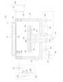
[0025]図1は、本技術のいくつかの実施形態による例示的な処理チャンバ100の断面図を示している。該図は、本技術の1つ又は複数の態様を組み込んだ、及び/又は本技術の実施形態による1つ又は複数の動作を実行するように特別に構成され得るシステムの概要を示し得る。チャンバ100又は実施される方法の追加の詳細は、以下で更に説明され得る。チャンバ100は、本技術のいくつかの実施形態に従ってフィルム層を形成するために利用され得るが、方法は、フィルム形成が起こり得る任意のチャンバにおいて同様に実行され得ることが理解されるべきである。処理チャンバ100は、チャンバ本体102、チャンバ本体102の内部に配置された基板支持体104、及びチャンバ本体102と結合され、処理領域(processing volume)120内に基板支持体104を封入するリッドアセンブリ106を含んでよい。基板103は、開口部126を介して処理領域120に設けることができ、開口部126は、スリットバルブ又はドアを使用して処理するために従来の方法で密封することができる。基板103は、処理中に基板支持体の表面105上に取り付けることができる。基板支持体104は、矢印145によって示されるように、軸147に沿って回転可能であることができ、ここで、基板支持体104のシャフト144を配置することができる。あるいはまた、基板支持体104は、堆積プロセス中に必要に応じて回転するように持ち上げることができる。[0025] FIG. 1 illustrates a cross-sectional view of an exemplary processing chamber 100 according to some embodiments of the present technique. The diagram may provide an overview of a system that may incorporate one or more aspects of the present technique and/or be specifically configured to perform one or more operations according to embodiments of the present technique. Additional details of the chamber 100 or the method performed may be further described below. Although the chamber 100 may be utilized to form a film layer according to some embodiments of the present technique, it should be understood that the method may similarly be performed in any chamber in which film formation may occur. The processing chamber 100 may include a
[0026]プラズマプロファイル変調器111は、基板支持体104上に配置された基板103を横切るプラズマ分布を制御するために、処理チャンバ100内に配置され得る。プラズマプロファイル変調器111は、チャンバ本体102に隣接して配置され得る第1の電極108を含むことができ、そしてチャンバ本体102をリッドアセンブリ106の他の構成要素から分離させることができる。第1の電極108は、リッドアセンブリ106の一部であり得るか、又は別個の側壁電極であり得る。例えば、以下で更に説明されるいくつかの実施形態では、第1の電極108は、フェースプレートであり得る。第1の電極108は、環状又はリング状の部材であり得、リング電極であり得る。第1の電極108は、処理領域120を取り囲む処理チャンバ100の円周の周りの連続ループであり得るか、又は必要に応じて選択された位置で不連続であり得る。第1の電極108はまた、有孔リング又はメッシュ電極などの有孔電極であり得るか、あるいは、例えば、二次ガス分配器などのプレート電極であり得る。[0026] A
[0027]セラミック又は金属酸化物、例えば酸化アルミニウム及び/又は窒化アルミニウムなどの誘電体材料であり得る1つ又は複数のアイソレータ110a、110bは、第1の電極108に接触し、第1の電極108をガス分配器112及びチャンバ本体102から電気的及び熱的に分離することができる。ガス分配器112は、プロセス前駆体を処理領域120に分配するための開孔118を画定することができる。ガス分配器112は、RF発生器、RF電源、DC電源、パルスDC電源、パルスRF電源、又は処理室と結合可能な任意の他の電源などの第1の電源142と結合することができる。いくつかの実施形態では、第1の電源142は、RF電源であり得る。[0027] One or more isolators 110a, 110b, which may be a dielectric material such as a ceramic or metal oxide, e.g., aluminum oxide and/or aluminum nitride, may contact the first electrode 108 and electrically and thermally isolate the first electrode 108 from the gas distributor 112 and the
[0028]ガス分配器112は、導電性ガス分配器又は非導電性ガス分配器であり得る。ガス分配器112はまた、導電性及び非導電性構成要素から形成され得る。例えば、ガス分配器112の本体は導電性であり得るが、ガス分配器112のフェースプレートは非導電性であってよい。ガス分配器112は、例えば、図1に示されるような第1の電力源142によって電力を供給され得るか、又はガス分配器112は、いくつかの実施形態において、地面と結合され得る。[0028] The gas distributor 112 can be a conductive gas distributor or a non-conductive gas distributor. The gas distributor 112 can also be formed from conductive and non-conductive components. For example, the body of the gas distributor 112 can be conductive, while the faceplate of the gas distributor 112 can be non-conductive. The gas distributor 112 can be powered, for example, by a
[0029]第1の電極108は、処理チャンバ100の接地経路を制御することができる第1の調整回路128と結合することができる。第1の調整回路128は、第1の電子センサ130及び第1の電子コントローラ134を含み得る。第1の電子コントローラ134は、可変コンデンサ又は他の回路要素であり得るか、あるいはそれらを含み得る。第1の調整回路128は、1つ又は複数のインダクタ132であり得るか、あるいはそれらを含み得る。第1の調整回路128は、処理中に処理領域120に存在するプラズマ条件下で可変又は制御可能なインピーダンスを可能にする任意の回路であり得る。図示のいくつかの実施形態では、第1の調整回路128は、接地と第1の電子センサ130との間に並列に結合された第1の回路脚及び第2の回路脚を含み得る。第1の回路脚は、第1のインダクタ132Aを含み得る。第2の回路脚は、第1の電子コントローラ134と直列に結合された第2のインダクタ132Bを含み得る。第2のインダクタ132Bは、第1の電子コントローラ134と、第1及び第2の回路脚の両方を第1の電子センサ130に接続するノードとの間に配置することができる。第1の電子センサ130は、電圧又は電流センサであることができ、第1の電子コントローラ134と結合することができ、これは、処理領域120内のプラズマ状態のある程度の閉ループ制御を可能にし得る。[0029] The first electrode 108 can be coupled to a
[0030]第2の電極122は、基板支持体104と結合され得る。第2の電極122は、基板支持体104内に埋め込まれるか、又は基板支持体104の表面と結合され得る。第2の電極122は、プレート、穴あきプレート、メッシュ、ワイヤスクリーン、又は導電性要素の他の任意の分散配置であり得る。第2の電極122は、調整電極であることができ、例えば、基板支持体104のシャフト144に配置されている、例えば、50オームなどの選択された抵抗を持つケーブルなどの導管146によって第2の調整回路136と結合することができる。第2の調整回路136は、第2の電子センサ138と、第2の可変コンデンサであり得る第2の電子コントローラ140とを有することができる。第2の電子センサ138は、電圧又は電流センサであることができ、第2の電子コントローラ140と結合されて、処理領域120内のプラズマ状態を更に制御することができる。[0030] The second electrode 122 may be coupled to the
[0031]バイアス電極及び/又は静電チャッキング電極であり得る第3の電極124は、基板支持体104と結合され得る。第3の電極は、インピーダンス整合回路であり得るフィルタ148を介して第2の電力源150と結合され得る。第2の電力源150は、DC電力、パルスDC電力、RFバイアス電力、パルスRF源又はバイアス電力、あるいはこれら若しくは他の電源の組み合わせであり得る。いくつかの実施形態では、第2の電力源150は、RFバイアス電力であり得る。[0031] A third electrode 124, which may be a bias electrode and/or an electrostatic chucking electrode, may be coupled to the
[0032]図1のリッドアセンブリ106及び基板支持体104は、プラズマ又は熱処理のための任意の処理チャンバと共に使用することができる。動作中、処理チャンバ100は、処理領域120内のプラズマ状態のリアルタイム制御を提供することができる。基板103は、基板支持体104上に配置することができ、プロセスガスは、任意の所望のフロープランに従って、入口114を使用して、リッドアセンブリ106を通って流れることができる。ガスは、出口152を通って処理チャンバ100を出ることができる。電力は、ガス分配器112と結合されて、処理領域120内にプラズマを確立することができる。いくつかの実施形態では、基板は、第3の電極124を使用して電気的バイアスに供することができる。[0032] The lid assembly 106 and
[0033]処理ボリューム120内のプラズマにエネルギーを与えると、プラズマと第1の電極108との間に電位差が確立され得る。電位差はまた、プラズマと第2の電極122との間に確立され得る。次に、電子コントローラ134、140を使用して、2つの調整回路128及び136によって表される接地経路の流動特性を調整することができる。設定点は、第1の調整回路128及び第2の調整回路136に供給されて、堆積速度及び中心から端までのプラズマ密度の均一性の独立した制御を提供することができる。電子コントローラが両方とも可変コンデンサであり得る実施形態では、電子センサは、堆積速度を最大化し、厚さの不均一性を独立して最小化するように可変コンデンサを調整することができる。[0033] Upon energizing the plasma in the process volume 120, a potential difference may be established between the plasma and the first electrode 108. A potential difference may also be established between the plasma and the second electrode 122. Electronic controllers 134, 140 may then be used to adjust the flow characteristics of the ground paths represented by the two
[0034]調整回路128、136のそれぞれは、それぞれの電子コントローラ134、140を使用して調整することができる可変インピーダンスを有することができる。電子コントローラ134、140が可変コンデンサである場合、各可変コンデンサの静電容量範囲、及び第1のインダクタ132Aと第2のインダクタ132Bのインダクタンスを選択して、インピーダンス範囲を提供することができる。この範囲は、プラズマの周波数及び電圧特性に依存する可能性があり、各可変コンデンサの静電容量範囲が最小になる可能性がある。したがって、第1の電子コントローラ134の静電容量が最小又は最大である場合、第1の調整回路128のインピーダンスは高くなり得、その結果、基板支持体上に最小の空中又は横方向の及ぶ範囲を有するプラズマ形状が生ずる。第1の電子コントローラ134の静電容量が第1の調整回路128のインピーダンスを最小化する値に近づくと、プラズマの空中の及ぶ範囲は最大になり、基板支持体104の作業領域全体を効果的に覆うことができる。第1の電子コントローラ134の静電容量が最小インピーダンス設定から逸脱するにつれて、プラズマ形状がチャンバ壁から収縮する可能性があり、基板支持体の空中の及ぶ範囲が低下する可能性がある。第2の電子制御装置140は、同様の効果を有し得、第2の電子コントローラ140の静電容量が変化し得るので、基板支持体上のプラズマの空中の及ぶ範囲を増加及び減少させることができる。[0034] Each of the
[0035]電子センサ130、138は、閉ループでそれぞれの回路128、136を調整するために使用され得る。使用するセンサタイプに応じて、電流又は電圧の設定値を各センサに取り付けることができ、センサは、設定点からの逸脱を最小にするために、それぞれの電子コントローラ134、140への調整を決定する制御ソフトウェアを備えていてもよい。その結果、プラズマ形状が選択され、処理中に動的に制御され得る。前述の議論は、可変コンデンサである可能性がある電子コントローラ134、140に基づいているが、調整可能な特性を備えた任意の電子部品を使用して、調整可能なインピーダンスを調整回路128及び136に提供することができることは理解されるべきである。[0035]
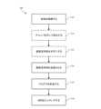
[0036]図2は、本技術のいくつかの実施形態による処理方法200における例示的な動作を示している。この方法は、上記の処理チャンバ100を含む様々な処理チャンバで実施することができる。方法200は、本技術による方法のいくつかの実施形態に具体的に関連付けられてもされなくてもよい、いくつかの任意の操作を含み得る。例えば、操作の多くは、構造形成のより広い範囲を提供するために説明されているが、技術にとって重要ではないか、又は容易に理解されるように代替の方法論によって実行され得る。方法200は、図3A~図3Bに概略的に示される処理チャンバ300で実行されるように示される操作を説明することができ、その図は、方法200の操作と併せて説明される。チャンバ300は、上記のチャンバ100の任意の態様を含み得る。図は部分的な概略図のみを示しており、基板は、図に示されているような側面を有する任意の数の構造セクション、並びに本技術の操作から依然として利益を得ることができる代替の構造的側面を含み得ることが理解されるべきである。[0036] FIG. 2 illustrates exemplary operations in a
[0037]方法200は、リストされた操作の開始前に追加の操作を含み得る。例えば、追加の処理操作は、半導体基板上に構造を形成することを含み得、これは、材料の形成及び除去の両方を含み得る。前処理操作は、方法200が実行され得るチャンバ内で実行され得るか、又は処理は、方法200が実行され得る半導体処理チャンバに基板を送達する前に、1つ又は複数の他の処理チャンバにおいて実行され得る。いずれにせよ、方法200は、任意選択で、半導体基板を、上記の処理チャンバ100などの半導体処理チャンバ、又は上記の構成要素を含み得る他のチャンバの処理領域に送達することを含み得る。基板は、基板支持体104などのペデスタルであり得る基板支持体上に堆積することができ、そしてそれは、上記の処理領域120などのチャンバの処理領域に存在し得る。例示的な基板305は、図3Aに示され、本技術による動作が実行され得る基板の態様であるか、又はそれを含むことができる。[0037]
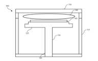
[0038]基板305は任意の数の材料であってよく、その上に材料を堆積することができる。基板は、シリコン、ゲルマニウム、酸化ケイ素若しくは窒化ケイ素を含む誘電体材料、金属材料、又はこれらの材料の任意の数の組み合わせであるか、又はそれらを含むことができ、これは、基板305、あるいは基板305上に形成された材料であり得る。チャンバ300は、前駆体が処理のために送達することができ、そしてチャンバの処理領域内にプラズマを生成するための電源と結合することができる、フェースプレート310を含む処理チャンバを含むことができる。チャンバはまた、図示のように側壁及びベースを含み得るチャンバ本体315を含み得る。ペデスタル又は基板支持体310は、前述のように、チャンバのベースを通って延在させることができる。処理領域は、ペデスタル、フェースプレート、及び/又はチャンバ壁の間に少なくとも部分的に画定することができる。基板支持体は、半導体基板305を支持することができる支持プラテン325を含み得る。支持プラテン325は、シャフト330と結合させることができ、シャフト330は、チャンバのベースを通って延在させることができる。[0038] The
[0039]方法200は、処理のためのチャンバを準備するための多数の操作、及びハードマスクフィルムを形成すること、又は他の堆積操作を含むことができるが、他の任意の堆積処理も同様に本技術に包含することができる。操作205で、材料を基板上に堆積することができる。堆積中、基板支持体310は、フェースプレート310に対して第1の垂直位置であり得る第1の位置に配置することができる。位置は、図に示されているように、基板支持体を横切るプラズマの発生を容易にするフェースプレートからの任意の距離であってよい。いくつかの操作では基板を傾けることもでき、これにより、チャンバの特徴を説明するための均一性の向上が促進される場合がある。基板の第1の位置は、容量結合プラズマが生成され得る、フェースプレートと基板支持体との間にプラズマ体積340を生成するように構成された高さであってよい。[0039]
[0040]1つの非限定的な実施形態では、堆積は、炭素含有ハードマスクの場合などのハードマスク堆積であり得る。炭素含有前駆体を処理領域に送達することができ、プラズマを生成して炭素含有ラジカルを生成することができ、これを基板上に堆積又は吸着させて、ハードマスクなどの炭素含有膜を生成することができる。任意の炭素含有材料を堆積に使用することができ、炭素含有前駆体は、任意のアルカン、アルケン、又は任意の他の炭素含有材料であるか、又はそれらを含むことができる。前駆体は、炭素-水素含有前駆体を含むことができ、これは、任意の量の炭素及び水素結合を含み得る。いくつかの実施形態では、炭素含有前駆体は、炭素-炭素結合及び炭素-水素結合からなるものであってよい。堆積は、基板上で均一に、又は比較的均一に発生する可能性があり、基板の上又は斜面エッジまでを含むエッジ領域に延在させることができる。堆積は、実行されている特定の堆積に基づいて調整され得る任意の数の処理条件で実行され得る。例 えば、炭素含有ハードマスクの場合、プロセスは、約600℃以上、約650℃以上、又はそれよりも高い温度で起こり得る。更に、チャンバ内の圧力は、約1~約20Torrの間に維持することができ、これは、例えば、約3~約9Torrなど、この範囲内の任意のより小さな範囲を含み得る。[0040] In one non-limiting embodiment, the deposition can be a hardmask deposition, such as in the case of a carbon-containing hardmask. A carbon-containing precursor can be delivered to the processing region, and a plasma can be generated to generate carbon-containing radicals, which can be deposited or adsorbed on the substrate to generate a carbon-containing film, such as a hardmask. Any carbon-containing material can be used for the deposition, and the carbon-containing precursor can be or include any alkane, alkene, or any other carbon-containing material. The precursor can include a carbon-hydrogen-containing precursor, which can include any amount of carbon and hydrogen bonds. In some embodiments, the carbon-containing precursor can be comprised of carbon-carbon bonds and carbon-hydrogen bonds. The deposition can occur uniformly or relatively uniformly on the substrate, and can extend to the edge region, including over or up to the bevel edge of the substrate. The deposition can be performed at any number of processing conditions, which can be adjusted based on the particular deposition being performed. For example, in the case of a carbon-containing hardmask, the process can occur at temperatures of about 600° C. or higher, about 650° C. or higher, or higher. Further, the pressure in the chamber can be maintained between about 1 and about 20 Torr, which can include any smaller range within this range, such as, for example, about 3 to about 9 Torr.
[0041]任意の厚さまで実行することができる堆積に続いて、任意の操作210で、チャンバをポンプダウンして、残留堆積前駆体又は堆積副生成物を除去することができる。例えば、チャンバは、残留物質を排出するために、約3Torr以下、約2Torr以下、約1Torr以下、又はそれより低くポンプダウンされ得る。更に、平坦化操作を実行して、基板が堆積中に傾斜していた場合のように、基板をフェースプレートと平行に又は実質的に平行にすることができる。実質的に平行とは、機械の公差に基づいて完全な平行性が実現できない可能性があることを意味し、許容誤差は、フェースプレートに対する完全な平面からのわずかな偏差を説明するための用語に含まれる。基板支持プラテン325及び基板は、任意の操作215で水平にすることができ、これは、その後の並進動作を容易にすることができる。[0041] Following deposition, which may be performed to any thickness, in
[0042]操作220において、基板支持体は垂直に並進させることができる。例えば、基板支持体は、フェースプレート310に向かって持ち上げることができ、フェースプレートに対して第1の位置から第2の位置に移動することができる。第2の位置は、図3Bに示されるように、支持体が第1の位置にあるときの基板支持体とフェースプレートとの間の距離よりも短い距離であるなど、いくつかの実施形態ではフェースプレートにより近い場合がある。以下で更に説明するように、この距離は、基板とフェースプレートとの間のプラズマ生成を制限するのに十分である可能性がある。エッチングプロセスを開始するために、エッチャント前駆体をチャンバに流入させることができる。エッチングされる材料に応じて、任意の数のエッチャント材料を実施形態で使用することができる。例えば、炭素含有フィルムの場合、酸素含有前駆体をチャンバに流入して、エッチャントとして使用することができる。本技術全体で説明されるような任意の操作で使用される酸素含有前駆体は、O2、N2O、NO2、O3、H2O、オゾン、並びフィルムエッチング、又はその他のフィルム変換若しくは除去操作で使用できる他の任意の酸素含有前駆体を含むことができる。いくつかの実施形態では、遠隔プラズマは、エッチャント前駆体から形成されない場合がある。遠隔プラズマが生成されると、プラズマ流出物はチャンバ構成要素を通って流れる可能性があり、基板全体に均一に分布する可能性がある。これは、斜角エッチングが望まれる可能性があるエッジ領域と同じかそれ以上の中央領域でフィルムをエッチングする可能性がある。 [0042] In
[0043]操作225において、プラズマは、チャンバの処理領域内のエッチャント前駆体から生成され得る。例えば、酸素含有前駆体の場合、酸素含有前駆体は、フェースプレートを通ってチャンバの処理領域に流入させることができる。プラズマは、基板支持体の位置によって影響を受ける可能性があるが、酸素含有前駆体に衝突する可能性がある。2つのプラズマ電極は、フェースプレート及び基板支持体であり得るか、又はそれらを含み得る。例えば、フェースプレートは、電力を供給されるRF電極として動作することができるが、いくつかの実施形態では、基板支持体は、フェースプレートに対してホット電極として動作することができる。前述のように、基板支持体は、プラズマ生成を制限するために、基板をフェースプレートから離れた位置に配置することができる。容量結合プラズマは、プラズマシースの距離を超えて間隔を空けることができる2つの電極の間に生成され得る。容量性プラズマでは、各電極は、バルク領域空間と電極の固体表面との間の遷移でプラズマシースを形成することができる。被覆に対応するために数デバイ長の距離を下回ると、プラズマが形成されない場合がある。したがって、基板を数デバイ長未満の距離に配置することにより、基板とフェースプレートとの間にプラズマが生成されない場合がある。[0043] In
[0044]したがって、いくつかの実施形態では、基板支持体が第2の位置にあるとき、フェースプレートに面する基板の表面は、フェースプレートから約5mm以下に位置付けることができ、フェースプレートから約4mm以下、約3mm以下、約2mm以下、1mm以下、又はそれ未満に位置付けることができる。チャンバのダイナミクスに応じて、プラズマシースは、各電極から約0.5mm以上~約1mmの距離で基板を横切って形成することができ、したがって、電極間の合計距離は約1mmと約2mmとの間である。その結果、基板をこの距離又はその範囲内に維持することにより、プラズマが基板とフェースプレートとの間に生成されない可能性がある。[0044] Thus, in some embodiments, when the substrate support is in the second position, the surface of the substrate facing the faceplate can be positioned about 5 mm or less from the faceplate, about 4 mm or less, about 3 mm or less, about 2 mm or less, 1 mm or less, or less from the faceplate. Depending on the dynamics of the chamber, a plasma sheath can form across the substrate at a distance of about 0.5 mm or more to about 1 mm from each electrode, such that the total distance between the electrodes is between about 1 mm and about 2 mm. As a result, by maintaining the substrate at this distance or within that range, plasma may not be generated between the substrate and the faceplate.
[0045]しかしながら、平面基板支持体、又は凹型ポケット若しくはエッジリングを備えた基板支持体の場合、基板支持体をフェースプレートの近くに配置することにより、プラズマは領域内に全く生成されない可能性がある。したがって、いくつかの実施形態では、基板支持体は、図示のように、支持体のエッジ領域にある凹んだレッジによって特徴付けることができる。いくつかのデバイ長を超えて延び得るエッジ距離を作成することにより、プラズマは、中央領域から制限されながら、エッジ領域の周りに形成することができる。結果として、エッチングは、形成されたフィルムの残りを実質的に維持しながら、基板の斜角及び/又はエッジ領域の周りで実行され得る。形成されたプラズマは、基板の周りに延在している環状形状によって特徴付けることができ、操作230でエッジ材料をエッチングできる。[0045] However, for planar substrate supports or substrate supports with recessed pockets or edge rings, by placing the substrate support close to the faceplate, plasma may not be generated in the region at all. Thus, in some embodiments, the substrate support may be characterized by a recessed ledge at the edge region of the support, as shown. By creating an edge distance that may extend beyond several Debye lengths, plasma may form around the edge region while being confined from the central region. As a result, etching may be performed around the bevel and/or edge region of the substrate while substantially preserving the remainder of the formed film. The formed plasma may be characterized by an annular shape extending around the substrate, and edge material may be etched in
[0046]上記のように、プラズマを生成するために、凹んだレッジとフェースプレートとの間の距離は、基板支持体が第2の位置にある間にプラズマを生成するのに十分であることができる。したがって、凹みは、約1mm以上、約2mm以上、約3mm以上、約4mm以上、又はそれより大きいものであることができる。図3Bに示されるように、凹んだレッジ345は、環状又は他の形状のプラズマ350が基板支持体の周りに形成され得るように、フェースプレートから十分に延在させることができる。これにより、基板の斜角がエッチングされ、堆積したフィルムの張り出しを除去できる。更に、基板と基板支持体との間の距離を増加させることにより、生成されたプラズマは、少なくとも部分的に半径方向内側に延在させることができ、これにより、基板のエッジ領域でのエッチングの制御された伸長が可能になる。例えば、エッチングは、基板の外側エッジから約50mm以下の距離で実施することができ、約45mm以下、約40mm以下、約35mm以下、約30mm以下、約25mm以下、約20mm以下、約15mm以下、約10mm以下、約5mm以下、約2mm以下、又はそれより短い距離に制御することができる。プラズマは密度勾配のために中心に拡散する可能性があるが、中心に到達したり、生成されたバルクフィルムの公称エッチングを超えたりすることはほとんどない。[0046] As described above, to generate a plasma, the distance between the recessed ledge and the faceplate can be sufficient to generate a plasma while the substrate support is in the second position. Thus, the recess can be about 1 mm or more, about 2 mm or more, about 3 mm or more, about 4 mm or more, or more. As shown in FIG. 3B, the recessed
[0047]図4は、本技術のいくつかの実施形態による例示的な基板支持体400の概略上面平面図を示している。基板支持体400は、他の場所で議論される任意の基板支持体の追加の図であり得、議論される任意のチャンバ、又は半導体処理で使用され得る任意の他のチャンバに含まれ得る。図示のように、基板支持体400は、支持体の中央領域405に基板402を取り付けることができる。凹んだレッジ410は、斜面エッチング用のプラズマ生成領域を生成するために、基板支持体の周りに延在させることができる。図示のように、凹んだレッジ410は、基板から外側にある距離だけ延在させることができ、基板の端から約5mm以上、約10mm以上、約15mm以上、約20mm以上、約25mm以上、30mm以上、又はそれ以上延在させることができる。[0047] FIG. 4 shows a schematic top plan view of an
[0048]多くの基板支持体には、ウエハ用のポケット又はエッジリングが含まれており、これらは両方とも、他の利点の中でも特に位置上の利点を提供することができる。例えば、チャンバの排気及び加圧中に、基板の位置を維持するための適切な取付け又は構成要素がないと、基板は、基板支持体上でシフト又は浮遊する可能性があり、これは、中心軸からオフセットされたウエハ上のプロセスの均一性に影響を与える可能性がある。凹んだレッジのあるヒーターを利用することにより、エッジリングやポケットのような側面が利用できない場合がある。したがって、本技術のいくつかの実施形態は、位置決めタブ415を組み込むことができ、これは、凹んだ外側レッジがあっても、処理中に基板が所定の位置に維持されることを確実にすることができる。タブは、斜面でのエッチングプロセスへの影響を制限するために、制限された垂直方向の延長によって形成又は包含され、特徴付けることができる。したがって、いくつかの実施形態では、タブは、基板が取り付けられる表面の上の高さが約20mm以下であることによって特徴付けることができ、表面からの、約15mm以下、約12mm以下、約10mm以下、約9mm以下、約8mm以下、約7mm以下、約6mm以下、約5mm以下、約4mm以下、約3mm以下、約2mm以下、又はそれよりを下回る高さによって特徴付けることができる。基板支持体上に凹んだレッジを含めることにより、本技術は、制御されたエッジプラズマ及びエッチングを生成することを可能にし得る。そのようなプラズマは、堆積が基板上に実行された単一のチャンバ内でその場でのエッチングを実行することを可能にし得る。[0048] Many substrate supports include a pocket or edge ring for the wafer, both of which can provide positional advantages, among other benefits. For example, without the proper mounting or components to maintain the position of the substrate during evacuation and repressurization of the chamber, the substrate may shift or float on the substrate support, which can affect process uniformity on wafers offset from the central axis. By utilizing a heater with a recessed ledge, sides such as an edge ring or pocket may not be available. Thus, some embodiments of the present technology may incorporate a
[0049]前述の説明では、説明の目的で、本技術の様々な実施形態の理解を提供するために多くの詳細が示されている。しかしながら、当業者には、これらの詳細のうちの一部がなくても、あるいは、追加の詳細があれば、特定の実施形態を実施できることが明らかであろう。[0049] In the foregoing description, for purposes of explanation, numerous details are set forth to provide an understanding of various embodiments of the present technology. However, it will be apparent to one of ordinary skill in the art that certain embodiments may be practiced without some of these details or with additional details.
[0050]いくつかの実施形態を開示したが、当業者は、実施形態の趣旨から逸脱することなく、様々な修正、代替構造、及び等価物を使用できることが認識されるであろう。更に、本技術を不必要にあいまいにすることを避けるために、いくつかの周知のプロセス及び要素については説明しなかった。したがって、上記の説明は、本技術の範囲を制限するものとして解釈されるべきではない。[0050] Although several embodiments have been disclosed, those skilled in the art will recognize that various modifications, alternative constructions, and equivalents may be used without departing from the spirit of the embodiments. Moreover, some well-known processes and elements have not been described in order to avoid unnecessarily obscuring the technology. Thus, the above description should not be construed as limiting the scope of the technology.
[0051]値の範囲が提示される場合、文脈上明らかに別段の指示がない限り、その範囲の上限と下限の間の各介在値はまた、下限の単位の最小単位まで具体的に開示されることが理解される。記載された範囲の任意の記載値又は記載されていない介在値の間の任意の狭い範囲、そしてその記載範囲のその他任意の記載された又は介在する値も包含される。これらの小さい範囲の上限と下限は、個別に範囲に含めることも除外することもでき、いずれか、どちらでもない、又は両方の制限がより狭い範囲に含まれている各範囲も本技術に含まれ、指定された範囲で特に除外された制限が適用される。記載された範囲に制限の一方又は両方が含まれる場合、含まれる制限のいずれか又は両方を除く範囲も含まれる。[0051] When a range of values is presented, it is understood that each intervening value between the upper and lower limits of that range is also specifically disclosed to the nearest unit of the lower limit, unless the context clearly dictates otherwise. Any narrower ranges between any stated or unstated intervening value in a stated range, and any other stated or intervening value in that stated range, are also encompassed. The upper and lower limits of these smaller ranges may be individually included or excluded in the range, and each range in which either, neither, or both limits are included in the narrower range is also encompassed in the technology, subject to the specifically excluded limit in the stated range. When a stated range includes one or both of the limits, ranges excluding either or both of the included limits are also included.
[0052]本明細書及び添付の特許請求の範囲で使用されるように、単数形「1つの(a)」、「1つの(an)」、及び「その(the)」は、文脈上別途明示しない限り複数の指示物を含む。したがって、例えば、「前駆体」への言及は、複数のそのような前駆体への言及を含み、「層」への言及は、1つ又は複数の層、並びに当業者に知られているその等価物への言及などを含む。[0052] As used herein and in the appended claims, the singular forms "a," "an," and "the" include plural referents unless the context clearly indicates otherwise. Thus, for example, a reference to "a precursor" includes a reference to a plurality of such precursors, a reference to "a layer" includes a reference to one or more layers and equivalents thereof known to those skilled in the art, and so forth.
[0053]また、「含む(comprise(s))」、「含んでいる(comprising)」、「含有する(contain(s))」、「含有している(containing)」、「含む(include(s))」、及び「含んでいる(including)」という用語は、本明細書及び特許請求の範囲で使用された場合、記載された特徴、整数、構成要素、又はステップの存在を特定することを意図しているが、一又は複数のその他の特徴、整数、構成要素、工程、動作、又はグループの存在又は追加を除外するものではない。[0053] Additionally, the terms "comprise(s)", "comprising", "contain(s)", "containing", "include(s)", and "including", when used in this specification and claims, are intended to specify the presence of stated features, integers, components, or steps, but do not exclude the presence or addition of one or more other features, integers, components, steps, operations, or groups.
Claims (20)
Translated fromJapanese前記基板支持体を前記フェースプレートに対して第2の位置に持ち上げること;
前記半導体処理チャンバの前記処理領域内にエッチャント前駆体のプラズマを形成すること;及び
前記基板のエッジ領域をエッチングすること
を含む、半導体処理方法。 depositing material onto a substrate mounted on a substrate support contained in a processing region of a semiconductor processing chamber, the processing region being at least partially defined by the substrate support and a faceplate, the substrate support being at a first position within the processing region relative to the faceplate;
lifting the substrate support to a second position relative to the faceplate;
forming a plasma of an etchant precursor in the processing region of the semiconductor processing chamber; and etching an edge region of the substrate.
炭素含有前駆体を前記半導体処理チャンバの前記処理領域に送達すること、
前記炭素含有前駆体のプラズマを形成すること、及び
前記基板上に炭素含有材料を堆積すること
を含む、請求項1に記載の半導体処理方法。 The depositing step comprises:
delivering a carbon-containing precursor to the processing region of the semiconductor processing chamber;
The semiconductor processing method of claim 1 , comprising forming a plasma of the carbon-containing precursor; and depositing a carbon-containing material on the substrate.
前記基板支持体を、前記フェースプレートに面する前記基板の表面が前記フェースプレートから約5mm以下に位置付けられる位置まで持ち上げること;
前記半導体処理チャンバの前記処理領域内にエッチャント前駆体のプラズマを形成すること;及び
前記基板の中央領域に堆積された前記材料を実質的に維持しながら、前記基板のエッジ領域をエッチングすること
を含む、半導体処理方法。 depositing material onto a substrate mounted on a substrate support contained in a processing region of a semiconductor processing chamber, the processing region being defined at least in part by the substrate support and a faceplate, the substrate support being characterized by a recessed ledge at an outer edge of the substrate support;
raising the substrate support to a position such that a surface of the substrate facing the faceplate is positioned no more than about 5 mm from the faceplate;
forming a plasma of an etchant precursor in the processing region of the semiconductor processing chamber; and etching an edge region of the substrate while substantially maintaining the material deposited in a central region of the substrate.
酸素含有前駆体を前記半導体処理チャンバの前記処理領域に流入させること、
前記酸素含有前駆体のプラズマを形成すること、及び
前記酸素含有前駆体のプラズマ放出物で前記基板上に堆積された前記材料をエッチングすること
を含む、請求項10に記載の半導体処理方法。 Forming a plasma of an etchant precursor includes:
flowing an oxygen-containing precursor into the processing region of the semiconductor processing chamber;
11. The semiconductor processing method of claim 10, comprising forming a plasma of the oxygen-containing precursor; and etching the material deposited on the substrate with plasma effluents of the oxygen-containing precursor.
を更に含む、請求項10に記載の半導体処理方法。 11. The semiconductorprocessing method of claim 10, further comprising reducing the pressure in the semiconductor processing chamber subsequent to depositing the material to purge the processing region of the semiconductor processing chamber.
前記基板が前記フェースプレートと実質的に平行になるように、前記基板支持体を水平にすること
を更に含む、請求項10に記載の半導体処理方法。 The substrate support is characterized by tilt during deposition, and the method comprises:
The semiconductor processing method of claim 10 further comprising leveling the substrate support such that the substrate is substantially parallel to the faceplate.
前記基板支持体上に配置された基板上に炭素含有材料を堆積することであって、前記基板支持体は、前記フェースプレートに対して前記処理領域内の第1の位置にある、前記基板上に炭素含有材料を堆積すること;
前記基板支持体を前記フェースプレートに対して第2の位置に持ち上げること;
前記半導体処理チャンバの前記処理領域内に酸素含有前駆体の環状プラズマを形成すること;及び
前記基板のエッジ領域をエッチングすること
を含む、半導体処理方法。 forming a plasma of a carbon-containing precursor in a processing region of a semiconductor processing chamber, the processing region being defined at least in part by a substrate support and a faceplate;
depositing a carbon-containing material on a substrate disposed on the substrate support, the substrate support being at a first position within the processing region relative to the faceplate; depositing a carbon-containing material on the substrate;
lifting the substrate support to a second position relative to the faceplate;
forming an annular plasma of an oxygen-containing precursor in the processing region of the semiconductor processing chamber; and etching an edge region of the substrate.
Applications Claiming Priority (3)
| Application Number | Priority Date | Filing Date | Title |
|---|---|---|---|
| US16/700,758 | 2019-12-02 | ||
| US16/700,758US11139168B2 (en) | 2019-12-02 | 2019-12-02 | Chamber deposition and etch process |
| PCT/US2020/062595WO2021113178A1 (en) | 2019-12-02 | 2020-11-30 | Chamber deposition and etch process |
Publications (2)
| Publication Number | Publication Date |
|---|---|
| JP2023504673A JP2023504673A (en) | 2023-02-06 |
| JP7633255B2true JP7633255B2 (en) | 2025-02-19 |
Family
ID=76091754
Family Applications (1)
| Application Number | Title | Priority Date | Filing Date |
|---|---|---|---|
| JP2022533217AActiveJP7633255B2 (en) | 2019-12-02 | 2020-11-30 | Chamber Deposition and Etch Process |
Country Status (6)
| Country | Link |
|---|---|
| US (1) | US11139168B2 (en) |
| JP (1) | JP7633255B2 (en) |
| KR (1) | KR102779995B1 (en) |
| CN (1) | CN114930507A (en) |
| TW (1) | TWI780529B (en) |
| WO (1) | WO2021113178A1 (en) |
Families Citing this family (1)
| Publication number | Priority date | Publication date | Assignee | Title |
|---|---|---|---|---|
| US12131934B2 (en)* | 2020-10-05 | 2024-10-29 | Applied Materials, Inc. | Semiconductor substrate support leveling apparatus |
Citations (2)
| Publication number | Priority date | Publication date | Assignee | Title |
|---|---|---|---|---|
| US20090014127A1 (en) | 2007-07-12 | 2009-01-15 | Applied Materials, Inc. | Systems for plasma enhanced chemical vapor deposition and bevel edge etching |
| JP2017152689A (en) | 2016-02-05 | 2017-08-31 | ラム リサーチ コーポレーションLam Research Corporation | Chamber for patterning non-volatile metals |
Family Cites Families (22)
| Publication number | Priority date | Publication date | Assignee | Title |
|---|---|---|---|---|
| US6829056B1 (en)* | 2003-08-21 | 2004-12-07 | Michael Barnes | Monitoring dimensions of features at different locations in the processing of substrates |
| KR100572131B1 (en) | 2003-12-11 | 2006-04-18 | (주)울텍 | Plasma Etching Device for Simultaneously Etching the Edge, Side, and Bottom of a Silicon Wafer |
| KR20060060997A (en) | 2004-12-01 | 2006-06-07 | 삼성전자주식회사 | Wafer Edge Etching Equipment |
| US20070209684A1 (en)* | 2006-03-07 | 2007-09-13 | Applied Materials, Inc. | Copper deposition chamber having integrated bevel clean with edge bevel removal detection |
| US7718542B2 (en)* | 2006-08-25 | 2010-05-18 | Lam Research Corporation | Low-k damage avoidance during bevel etch processing |
| US8398778B2 (en)* | 2007-01-26 | 2013-03-19 | Lam Research Corporation | Control of bevel etch film profile using plasma exclusion zone rings larger than the wafer diameter |
| KR101342989B1 (en) | 2007-05-03 | 2013-12-18 | (주)소슬 | Equipment for etching substrate edge |
| CN101687229B (en)* | 2007-07-12 | 2012-01-18 | 应用材料股份有限公司 | Apparatus and method for centering a substrate in a process chamber |
| US20090302002A1 (en)* | 2008-02-29 | 2009-12-10 | Applied Materials, Inc. | Method and apparatus for removing polymer from a substrate |
| US20090293907A1 (en)* | 2008-05-28 | 2009-12-03 | Nancy Fung | Method of substrate polymer removal |
| US8658937B2 (en)* | 2010-01-08 | 2014-02-25 | Uvtech Systems, Inc. | Method and apparatus for processing substrate edges |
| CN103650118B (en)* | 2011-05-31 | 2016-08-24 | 应用材料公司 | Dynamic Ion Radical Sieve and Ion Radical Aperture in an Inductively Coupled Plasma (ICP) Reactor |
| WO2014052228A1 (en)* | 2012-09-26 | 2014-04-03 | Applied Materials, Inc. | Bottom and side plasma tuning having closed loop control |
| US9315891B2 (en)* | 2013-03-15 | 2016-04-19 | Applied Materials, Inc. | Methods for processing a substrate using multiple substrate support positions |
| US9564285B2 (en) | 2013-07-15 | 2017-02-07 | Lam Research Corporation | Hybrid feature etching and bevel etching systems |
| US10937634B2 (en)* | 2013-10-04 | 2021-03-02 | Lam Research Corporation | Tunable upper plasma-exclusion-zone ring for a bevel etcher |
| US10903066B2 (en)* | 2017-05-08 | 2021-01-26 | Applied Materials, Inc. | Heater support kit for bevel etch chamber |
| US10276364B2 (en)* | 2017-05-08 | 2019-04-30 | Applied Materials, Inc. | Bevel etch profile control |
| JP7326275B2 (en)* | 2017-12-01 | 2023-08-15 | アプライド マテリアルズ インコーポレイテッド | Amorphous carbon film with high etching selectivity |
| KR20200101833A (en)* | 2018-01-17 | 2020-08-28 | 에스피피 테크놀로지스 컴퍼니 리미티드 | Wide gap semiconductor substrate, manufacturing apparatus of wide gap semiconductor substrate, and manufacturing method of wide gap semiconductor substrate |
| JP2019140220A (en)* | 2018-02-09 | 2019-08-22 | 東芝メモリ株式会社 | Semiconductor processing device and semiconductor processing method |
| US20190341275A1 (en)* | 2018-05-07 | 2019-11-07 | Lam Research Corporation | Edge ring focused deposition during a cleaning process of a processing chamber |
- 2019
- 2019-12-02USUS16/700,758patent/US11139168B2/enactiveActive
- 2020
- 2020-11-30WOPCT/US2020/062595patent/WO2021113178A1/ennot_activeCeased
- 2020-11-30JPJP2022533217Apatent/JP7633255B2/enactiveActive
- 2020-11-30KRKR1020227022329Apatent/KR102779995B1/enactiveActive
- 2020-11-30CNCN202080092245.5Apatent/CN114930507A/enactivePending
- 2020-12-02TWTW109142312Apatent/TWI780529B/enactive
Patent Citations (2)
| Publication number | Priority date | Publication date | Assignee | Title |
|---|---|---|---|---|
| US20090014127A1 (en) | 2007-07-12 | 2009-01-15 | Applied Materials, Inc. | Systems for plasma enhanced chemical vapor deposition and bevel edge etching |
| JP2017152689A (en) | 2016-02-05 | 2017-08-31 | ラム リサーチ コーポレーションLam Research Corporation | Chamber for patterning non-volatile metals |
Also Published As
| Publication number | Publication date |
|---|---|
| JP2023504673A (en) | 2023-02-06 |
| CN114930507A (en) | 2022-08-19 |
| KR102779995B1 (en) | 2025-03-10 |
| US20210166942A1 (en) | 2021-06-03 |
| TW202137297A (en) | 2021-10-01 |
| US11139168B2 (en) | 2021-10-05 |
| WO2021113178A1 (en) | 2021-06-10 |
| TWI780529B (en) | 2022-10-11 |
| KR20220107045A (en) | 2022-08-01 |
Similar Documents
| Publication | Publication Date | Title |
|---|---|---|
| JP6050944B2 (en) | Plasma etching method and plasma processing apparatus | |
| US12412741B2 (en) | Silicon oxide gap fill using capacitively coupled plasmas | |
| JP2023502094A (en) | Edge Uniformity Tunability in Bipolar Electrostatic Chucks | |
| JP7633255B2 (en) | Chamber Deposition and Etch Process | |
| JP2022544230A (en) | Chamber configuration for controlled deposition | |
| JP7594587B2 (en) | A layer of material that encases the surface | |
| TWI826843B (en) | Electric arc mitigating faceplate | |
| KR102799704B1 (en) | Plasma-enhanced deposition of silicon-containing films at low temperatures | |
| JP2024519162A (en) | Boron Nitride for Mask Patterning | |
| US20230360924A1 (en) | Low temperature carbon gapfill | |
| US20220020589A1 (en) | Dielectric coating for deposition chamber | |
| TWI809496B (en) | High conductance process kit | |
| US11515150B2 (en) | Hardmask tuning by electrode adjustment | |
| JP2024511958A (en) | Systems and methods for improved carbon bonding | |
| JP2024519841A (en) | Low impedance current path for end face nonuniformity tuning | |
| KR20210059444A (en) | Method of forming stacked thin films and Apparatus for treating substrate |
Legal Events
| Date | Code | Title | Description |
|---|---|---|---|
| A621 | Written request for application examination | Free format text:JAPANESE INTERMEDIATE CODE: A621 Effective date:20231127 | |
| A977 | Report on retrieval | Free format text:JAPANESE INTERMEDIATE CODE: A971007 Effective date:20240814 | |
| A131 | Notification of reasons for refusal | Free format text:JAPANESE INTERMEDIATE CODE: A131 Effective date:20240820 | |
| A521 | Request for written amendment filed | Free format text:JAPANESE INTERMEDIATE CODE: A523 Effective date:20241119 | |
| TRDD | Decision of grant or rejection written | ||
| A01 | Written decision to grant a patent or to grant a registration (utility model) | Free format text:JAPANESE INTERMEDIATE CODE: A01 Effective date:20250107 | |
| A61 | First payment of annual fees (during grant procedure) | Free format text:JAPANESE INTERMEDIATE CODE: A61 Effective date:20250206 | |
| R150 | Certificate of patent or registration of utility model | Ref document number:7633255 Country of ref document:JP Free format text:JAPANESE INTERMEDIATE CODE: R150 |