JP7630598B2 - Semiconductor Device - Google Patents
Semiconductor DeviceDownload PDFInfo
- Publication number
- JP7630598B2 JP7630598B2JP2023215949AJP2023215949AJP7630598B2JP 7630598 B2JP7630598 B2JP 7630598B2JP 2023215949 AJP2023215949 AJP 2023215949AJP 2023215949 AJP2023215949 AJP 2023215949AJP 7630598 B2JP7630598 B2JP 7630598B2
- Authority
- JP
- Japan
- Prior art keywords
- oxide semiconductor
- film
- transistor
- insulating film
- region
- Prior art date
- Legal status (The legal status is an assumption and is not a legal conclusion. Google has not performed a legal analysis and makes no representation as to the accuracy of the status listed.)
- Active
Links
Images


Classifications
- H—ELECTRICITY
- H10—SEMICONDUCTOR DEVICES; ELECTRIC SOLID-STATE DEVICES NOT OTHERWISE PROVIDED FOR
- H10D—INORGANIC ELECTRIC SEMICONDUCTOR DEVICES
- H10D30/00—Field-effect transistors [FET]
- H10D30/60—Insulated-gate field-effect transistors [IGFET]
- H10D30/67—Thin-film transistors [TFT]
- H10D30/674—Thin-film transistors [TFT] characterised by the active materials
- H10D30/6755—Oxide semiconductors, e.g. zinc oxide, copper aluminium oxide or cadmium stannate
- H—ELECTRICITY
- H01—ELECTRIC ELEMENTS
- H01L—SEMICONDUCTOR DEVICES NOT COVERED BY CLASS H10
- H01L21/00—Processes or apparatus adapted for the manufacture or treatment of semiconductor or solid state devices or of parts thereof
- H01L21/02—Manufacture or treatment of semiconductor devices or of parts thereof
- H01L21/02104—Forming layers
- H01L21/02107—Forming insulating materials on a substrate
- H01L21/02109—Forming insulating materials on a substrate characterised by the type of layer, e.g. type of material, porous/non-porous, pre-cursors, mixtures or laminates
- H01L21/02112—Forming insulating materials on a substrate characterised by the type of layer, e.g. type of material, porous/non-porous, pre-cursors, mixtures or laminates characterised by the material of the layer
- H01L21/02123—Forming insulating materials on a substrate characterised by the type of layer, e.g. type of material, porous/non-porous, pre-cursors, mixtures or laminates characterised by the material of the layer the material containing silicon
- H01L21/02126—Forming insulating materials on a substrate characterised by the type of layer, e.g. type of material, porous/non-porous, pre-cursors, mixtures or laminates characterised by the material of the layer the material containing silicon the material containing Si, O, and at least one of H, N, C, F, or other non-metal elements, e.g. SiOC, SiOC:H or SiONC
- H01L21/0214—Forming insulating materials on a substrate characterised by the type of layer, e.g. type of material, porous/non-porous, pre-cursors, mixtures or laminates characterised by the material of the layer the material containing silicon the material containing Si, O, and at least one of H, N, C, F, or other non-metal elements, e.g. SiOC, SiOC:H or SiONC the material being a silicon oxynitride, e.g. SiON or SiON:H
- H—ELECTRICITY
- H01—ELECTRIC ELEMENTS
- H01L—SEMICONDUCTOR DEVICES NOT COVERED BY CLASS H10
- H01L21/00—Processes or apparatus adapted for the manufacture or treatment of semiconductor or solid state devices or of parts thereof
- H01L21/02—Manufacture or treatment of semiconductor devices or of parts thereof
- H01L21/02104—Forming layers
- H01L21/02107—Forming insulating materials on a substrate
- H01L21/02109—Forming insulating materials on a substrate characterised by the type of layer, e.g. type of material, porous/non-porous, pre-cursors, mixtures or laminates
- H01L21/02112—Forming insulating materials on a substrate characterised by the type of layer, e.g. type of material, porous/non-porous, pre-cursors, mixtures or laminates characterised by the material of the layer
- H01L21/02123—Forming insulating materials on a substrate characterised by the type of layer, e.g. type of material, porous/non-porous, pre-cursors, mixtures or laminates characterised by the material of the layer the material containing silicon
- H01L21/02164—Forming insulating materials on a substrate characterised by the type of layer, e.g. type of material, porous/non-porous, pre-cursors, mixtures or laminates characterised by the material of the layer the material containing silicon the material being a silicon oxide, e.g. SiO2
- H—ELECTRICITY
- H01—ELECTRIC ELEMENTS
- H01L—SEMICONDUCTOR DEVICES NOT COVERED BY CLASS H10
- H01L21/00—Processes or apparatus adapted for the manufacture or treatment of semiconductor or solid state devices or of parts thereof
- H01L21/02—Manufacture or treatment of semiconductor devices or of parts thereof
- H01L21/02104—Forming layers
- H01L21/02107—Forming insulating materials on a substrate
- H01L21/02109—Forming insulating materials on a substrate characterised by the type of layer, e.g. type of material, porous/non-porous, pre-cursors, mixtures or laminates
- H01L21/02112—Forming insulating materials on a substrate characterised by the type of layer, e.g. type of material, porous/non-porous, pre-cursors, mixtures or laminates characterised by the material of the layer
- H01L21/02123—Forming insulating materials on a substrate characterised by the type of layer, e.g. type of material, porous/non-porous, pre-cursors, mixtures or laminates characterised by the material of the layer the material containing silicon
- H01L21/0217—Forming insulating materials on a substrate characterised by the type of layer, e.g. type of material, porous/non-porous, pre-cursors, mixtures or laminates characterised by the material of the layer the material containing silicon the material being a silicon nitride not containing oxygen, e.g. SixNy or SixByNz
- H—ELECTRICITY
- H01—ELECTRIC ELEMENTS
- H01L—SEMICONDUCTOR DEVICES NOT COVERED BY CLASS H10
- H01L21/00—Processes or apparatus adapted for the manufacture or treatment of semiconductor or solid state devices or of parts thereof
- H01L21/02—Manufacture or treatment of semiconductor devices or of parts thereof
- H01L21/02104—Forming layers
- H01L21/02107—Forming insulating materials on a substrate
- H01L21/02225—Forming insulating materials on a substrate characterised by the process for the formation of the insulating layer
- H01L21/0226—Forming insulating materials on a substrate characterised by the process for the formation of the insulating layer formation by a deposition process
- H01L21/02263—Forming insulating materials on a substrate characterised by the process for the formation of the insulating layer formation by a deposition process deposition from the gas or vapour phase
- H01L21/02271—Forming insulating materials on a substrate characterised by the process for the formation of the insulating layer formation by a deposition process deposition from the gas or vapour phase deposition by decomposition or reaction of gaseous or vapour phase compounds, i.e. chemical vapour deposition
- H01L21/02274—Forming insulating materials on a substrate characterised by the process for the formation of the insulating layer formation by a deposition process deposition from the gas or vapour phase deposition by decomposition or reaction of gaseous or vapour phase compounds, i.e. chemical vapour deposition in the presence of a plasma [PECVD]
- H—ELECTRICITY
- H01—ELECTRIC ELEMENTS
- H01L—SEMICONDUCTOR DEVICES NOT COVERED BY CLASS H10
- H01L21/00—Processes or apparatus adapted for the manufacture or treatment of semiconductor or solid state devices or of parts thereof
- H01L21/02—Manufacture or treatment of semiconductor devices or of parts thereof
- H01L21/02104—Forming layers
- H01L21/02365—Forming inorganic semiconducting materials on a substrate
- H01L21/02518—Deposited layers
- H01L21/02521—Materials
- H01L21/02551—Group 12/16 materials
- H01L21/02554—Oxides
- H—ELECTRICITY
- H01—ELECTRIC ELEMENTS
- H01L—SEMICONDUCTOR DEVICES NOT COVERED BY CLASS H10
- H01L21/00—Processes or apparatus adapted for the manufacture or treatment of semiconductor or solid state devices or of parts thereof
- H01L21/02—Manufacture or treatment of semiconductor devices or of parts thereof
- H01L21/02104—Forming layers
- H01L21/02365—Forming inorganic semiconducting materials on a substrate
- H01L21/02518—Deposited layers
- H01L21/02521—Materials
- H01L21/02565—Oxide semiconducting materials not being Group 12/16 materials, e.g. ternary compounds
- H—ELECTRICITY
- H01—ELECTRIC ELEMENTS
- H01L—SEMICONDUCTOR DEVICES NOT COVERED BY CLASS H10
- H01L21/00—Processes or apparatus adapted for the manufacture or treatment of semiconductor or solid state devices or of parts thereof
- H01L21/02—Manufacture or treatment of semiconductor devices or of parts thereof
- H01L21/02104—Forming layers
- H01L21/02365—Forming inorganic semiconducting materials on a substrate
- H01L21/02612—Formation types
- H01L21/02617—Deposition types
- H01L21/0262—Reduction or decomposition of gaseous compounds, e.g. CVD
- H—ELECTRICITY
- H01—ELECTRIC ELEMENTS
- H01L—SEMICONDUCTOR DEVICES NOT COVERED BY CLASS H10
- H01L21/00—Processes or apparatus adapted for the manufacture or treatment of semiconductor or solid state devices or of parts thereof
- H01L21/02—Manufacture or treatment of semiconductor devices or of parts thereof
- H01L21/02104—Forming layers
- H01L21/02365—Forming inorganic semiconducting materials on a substrate
- H01L21/02612—Formation types
- H01L21/02617—Deposition types
- H01L21/02631—Physical deposition at reduced pressure, e.g. MBE, sputtering, evaporation
- H—ELECTRICITY
- H01—ELECTRIC ELEMENTS
- H01L—SEMICONDUCTOR DEVICES NOT COVERED BY CLASS H10
- H01L21/00—Processes or apparatus adapted for the manufacture or treatment of semiconductor or solid state devices or of parts thereof
- H01L21/02—Manufacture or treatment of semiconductor devices or of parts thereof
- H01L21/04—Manufacture or treatment of semiconductor devices or of parts thereof the devices having potential barriers, e.g. a PN junction, depletion layer or carrier concentration layer
- H01L21/34—Manufacture or treatment of semiconductor devices or of parts thereof the devices having potential barriers, e.g. a PN junction, depletion layer or carrier concentration layer the devices having semiconductor bodies not provided for in groups H01L21/18, H10D48/04 and H10D48/07, with or without impurities, e.g. doping materials
- H01L21/46—Treatment of semiconductor bodies using processes or apparatus not provided for in groups H01L21/428
- H01L21/461—Treatment of semiconductor bodies using processes or apparatus not provided for in groups H01L21/428 to change their surface-physical characteristics or shape, e.g. etching, polishing, cutting
- H01L21/465—Chemical or electrical treatment, e.g. electrolytic etching
- H—ELECTRICITY
- H01—ELECTRIC ELEMENTS
- H01L—SEMICONDUCTOR DEVICES NOT COVERED BY CLASS H10
- H01L21/00—Processes or apparatus adapted for the manufacture or treatment of semiconductor or solid state devices or of parts thereof
- H01L21/02—Manufacture or treatment of semiconductor devices or of parts thereof
- H01L21/04—Manufacture or treatment of semiconductor devices or of parts thereof the devices having potential barriers, e.g. a PN junction, depletion layer or carrier concentration layer
- H01L21/34—Manufacture or treatment of semiconductor devices or of parts thereof the devices having potential barriers, e.g. a PN junction, depletion layer or carrier concentration layer the devices having semiconductor bodies not provided for in groups H01L21/18, H10D48/04 and H10D48/07, with or without impurities, e.g. doping materials
- H01L21/46—Treatment of semiconductor bodies using processes or apparatus not provided for in groups H01L21/428
- H01L21/461—Treatment of semiconductor bodies using processes or apparatus not provided for in groups H01L21/428 to change their surface-physical characteristics or shape, e.g. etching, polishing, cutting
- H01L21/469—Treatment of semiconductor bodies using processes or apparatus not provided for in groups H01L21/428 to change their surface-physical characteristics or shape, e.g. etching, polishing, cutting to form insulating layers thereon, e.g. for masking or by using photolithographic techniques; After-treatment of these layers
- H01L21/4757—After-treatment
- H01L21/47573—Etching the layer
- H—ELECTRICITY
- H01—ELECTRIC ELEMENTS
- H01L—SEMICONDUCTOR DEVICES NOT COVERED BY CLASS H10
- H01L21/00—Processes or apparatus adapted for the manufacture or treatment of semiconductor or solid state devices or of parts thereof
- H01L21/02—Manufacture or treatment of semiconductor devices or of parts thereof
- H01L21/04—Manufacture or treatment of semiconductor devices or of parts thereof the devices having potential barriers, e.g. a PN junction, depletion layer or carrier concentration layer
- H01L21/34—Manufacture or treatment of semiconductor devices or of parts thereof the devices having potential barriers, e.g. a PN junction, depletion layer or carrier concentration layer the devices having semiconductor bodies not provided for in groups H01L21/18, H10D48/04 and H10D48/07, with or without impurities, e.g. doping materials
- H01L21/46—Treatment of semiconductor bodies using processes or apparatus not provided for in groups H01L21/428
- H01L21/477—Thermal treatment for modifying the properties of semiconductor bodies, e.g. annealing, sintering
- H—ELECTRICITY
- H10—SEMICONDUCTOR DEVICES; ELECTRIC SOLID-STATE DEVICES NOT OTHERWISE PROVIDED FOR
- H10D—INORGANIC ELECTRIC SEMICONDUCTOR DEVICES
- H10D30/00—Field-effect transistors [FET]
- H10D30/60—Insulated-gate field-effect transistors [IGFET]
- H10D30/67—Thin-film transistors [TFT]
- H10D30/6704—Thin-film transistors [TFT] having supplementary regions or layers in the thin films or in the insulated bulk substrates for controlling properties of the device
- H10D30/6713—Thin-film transistors [TFT] having supplementary regions or layers in the thin films or in the insulated bulk substrates for controlling properties of the device characterised by the properties of the source or drain regions, e.g. compositions or sectional shapes
- H—ELECTRICITY
- H10—SEMICONDUCTOR DEVICES; ELECTRIC SOLID-STATE DEVICES NOT OTHERWISE PROVIDED FOR
- H10D—INORGANIC ELECTRIC SEMICONDUCTOR DEVICES
- H10D30/00—Field-effect transistors [FET]
- H10D30/60—Insulated-gate field-effect transistors [IGFET]
- H10D30/67—Thin-film transistors [TFT]
- H10D30/6729—Thin-film transistors [TFT] characterised by the electrodes
- H10D30/673—Thin-film transistors [TFT] characterised by the electrodes characterised by the shapes, relative sizes or dispositions of the gate electrodes
- H10D30/6733—Multi-gate TFTs
- H10D30/6734—Multi-gate TFTs having gate electrodes arranged on both top and bottom sides of the channel, e.g. dual-gate TFTs
- H—ELECTRICITY
- H10—SEMICONDUCTOR DEVICES; ELECTRIC SOLID-STATE DEVICES NOT OTHERWISE PROVIDED FOR
- H10D—INORGANIC ELECTRIC SEMICONDUCTOR DEVICES
- H10D30/00—Field-effect transistors [FET]
- H10D30/60—Insulated-gate field-effect transistors [IGFET]
- H10D30/67—Thin-film transistors [TFT]
- H10D30/6729—Thin-film transistors [TFT] characterised by the electrodes
- H10D30/6737—Thin-film transistors [TFT] characterised by the electrodes characterised by the electrode materials
- H10D30/6739—Conductor-insulator-semiconductor electrodes
- H—ELECTRICITY
- H10—SEMICONDUCTOR DEVICES; ELECTRIC SOLID-STATE DEVICES NOT OTHERWISE PROVIDED FOR
- H10D—INORGANIC ELECTRIC SEMICONDUCTOR DEVICES
- H10D30/00—Field-effect transistors [FET]
- H10D30/60—Insulated-gate field-effect transistors [IGFET]
- H10D30/67—Thin-film transistors [TFT]
- H10D30/6757—Thin-film transistors [TFT] characterised by the structure of the channel, e.g. transverse or longitudinal shape or doping profile
- H—ELECTRICITY
- H10—SEMICONDUCTOR DEVICES; ELECTRIC SOLID-STATE DEVICES NOT OTHERWISE PROVIDED FOR
- H10D—INORGANIC ELECTRIC SEMICONDUCTOR DEVICES
- H10D62/00—Semiconductor bodies, or regions thereof, of devices having potential barriers
- H10D62/40—Crystalline structures
- H10D62/405—Orientations of crystalline planes
- H—ELECTRICITY
- H10—SEMICONDUCTOR DEVICES; ELECTRIC SOLID-STATE DEVICES NOT OTHERWISE PROVIDED FOR
- H10D—INORGANIC ELECTRIC SEMICONDUCTOR DEVICES
- H10D62/00—Semiconductor bodies, or regions thereof, of devices having potential barriers
- H10D62/80—Semiconductor bodies, or regions thereof, of devices having potential barriers characterised by the materials
- H—ELECTRICITY
- H10—SEMICONDUCTOR DEVICES; ELECTRIC SOLID-STATE DEVICES NOT OTHERWISE PROVIDED FOR
- H10D—INORGANIC ELECTRIC SEMICONDUCTOR DEVICES
- H10D64/00—Electrodes of devices having potential barriers
- H10D64/60—Electrodes characterised by their materials
- H10D64/66—Electrodes having a conductor capacitively coupled to a semiconductor by an insulator, e.g. MIS electrodes
- H10D64/667—Electrodes having a conductor capacitively coupled to a semiconductor by an insulator, e.g. MIS electrodes the conductor comprising a layer of alloy material, compound material or organic material contacting the insulator, e.g. TiN workfunction layers
- H—ELECTRICITY
- H10—SEMICONDUCTOR DEVICES; ELECTRIC SOLID-STATE DEVICES NOT OTHERWISE PROVIDED FOR
- H10D—INORGANIC ELECTRIC SEMICONDUCTOR DEVICES
- H10D86/00—Integrated devices formed in or on insulating or conducting substrates, e.g. formed in silicon-on-insulator [SOI] substrates or on stainless steel or glass substrates
- H10D86/01—Manufacture or treatment
- H10D86/021—Manufacture or treatment of multiple TFTs
- H—ELECTRICITY
- H10—SEMICONDUCTOR DEVICES; ELECTRIC SOLID-STATE DEVICES NOT OTHERWISE PROVIDED FOR
- H10D—INORGANIC ELECTRIC SEMICONDUCTOR DEVICES
- H10D86/00—Integrated devices formed in or on insulating or conducting substrates, e.g. formed in silicon-on-insulator [SOI] substrates or on stainless steel or glass substrates
- H10D86/40—Integrated devices formed in or on insulating or conducting substrates, e.g. formed in silicon-on-insulator [SOI] substrates or on stainless steel or glass substrates characterised by multiple TFTs
- H10D86/421—Integrated devices formed in or on insulating or conducting substrates, e.g. formed in silicon-on-insulator [SOI] substrates or on stainless steel or glass substrates characterised by multiple TFTs having a particular composition, shape or crystalline structure of the active layer
- H10D86/423—Integrated devices formed in or on insulating or conducting substrates, e.g. formed in silicon-on-insulator [SOI] substrates or on stainless steel or glass substrates characterised by multiple TFTs having a particular composition, shape or crystalline structure of the active layer comprising semiconductor materials not belonging to the Group IV, e.g. InGaZnO
- H—ELECTRICITY
- H10—SEMICONDUCTOR DEVICES; ELECTRIC SOLID-STATE DEVICES NOT OTHERWISE PROVIDED FOR
- H10D—INORGANIC ELECTRIC SEMICONDUCTOR DEVICES
- H10D86/00—Integrated devices formed in or on insulating or conducting substrates, e.g. formed in silicon-on-insulator [SOI] substrates or on stainless steel or glass substrates
- H10D86/40—Integrated devices formed in or on insulating or conducting substrates, e.g. formed in silicon-on-insulator [SOI] substrates or on stainless steel or glass substrates characterised by multiple TFTs
- H10D86/60—Integrated devices formed in or on insulating or conducting substrates, e.g. formed in silicon-on-insulator [SOI] substrates or on stainless steel or glass substrates characterised by multiple TFTs wherein the TFTs are in active matrices
- H—ELECTRICITY
- H10—SEMICONDUCTOR DEVICES; ELECTRIC SOLID-STATE DEVICES NOT OTHERWISE PROVIDED FOR
- H10D—INORGANIC ELECTRIC SEMICONDUCTOR DEVICES
- H10D99/00—Subject matter not provided for in other groups of this subclass
- H—ELECTRICITY
- H10—SEMICONDUCTOR DEVICES; ELECTRIC SOLID-STATE DEVICES NOT OTHERWISE PROVIDED FOR
- H10K—ORGANIC ELECTRIC SOLID-STATE DEVICES
- H10K59/00—Integrated devices, or assemblies of multiple devices, comprising at least one organic light-emitting element covered by group H10K50/00
- H10K59/10—OLED displays
- H10K59/12—Active-matrix OLED [AMOLED] displays
- H10K59/1201—Manufacture or treatment
- H—ELECTRICITY
- H10—SEMICONDUCTOR DEVICES; ELECTRIC SOLID-STATE DEVICES NOT OTHERWISE PROVIDED FOR
- H10K—ORGANIC ELECTRIC SOLID-STATE DEVICES
- H10K59/00—Integrated devices, or assemblies of multiple devices, comprising at least one organic light-emitting element covered by group H10K50/00
- H10K59/10—OLED displays
- H10K59/12—Active-matrix OLED [AMOLED] displays
- H10K59/121—Active-matrix OLED [AMOLED] displays characterised by the geometry or disposition of pixel elements
- H10K59/1213—Active-matrix OLED [AMOLED] displays characterised by the geometry or disposition of pixel elements the pixel elements being TFTs
Landscapes
- Engineering & Computer Science (AREA)
- Manufacturing & Machinery (AREA)
- Physics & Mathematics (AREA)
- Microelectronics & Electronic Packaging (AREA)
- Condensed Matter Physics & Semiconductors (AREA)
- General Physics & Mathematics (AREA)
- Computer Hardware Design (AREA)
- Power Engineering (AREA)
- Chemical & Material Sciences (AREA)
- Chemical Kinetics & Catalysis (AREA)
- Plasma & Fusion (AREA)
- Thin Film Transistor (AREA)
- Devices For Indicating Variable Information By Combining Individual Elements (AREA)
- Composite Materials (AREA)
- Materials Engineering (AREA)
- Electroluminescent Light Sources (AREA)
- Solid State Image Pick-Up Elements (AREA)
- Liquid Crystal (AREA)
- Semiconductor Memories (AREA)
- Non-Volatile Memory (AREA)
Description
Translated fromJapanese 本発明の一態様は、酸化物半導体膜を有する半導体装置及び該半導体装置を有する表示
装置に関する。 One embodiment of the present invention relates to a semiconductor device including an oxide semiconductor film and a display device including the semiconductor device.
なお、本発明の一態様は、上記の技術分野に限定されない。本明細書等で開示する発明
の一態様の技術分野は、物、方法、または、製造方法に関する。または、本発明は、プロ
セス、マシン、マニュファクチャ、または、組成物(コンポジション・オブ・マター)に
関する。特に、本発明の一態様は、半導体装置、表示装置、発光装置、蓄電装置、記憶装
置、それらの駆動方法、またはそれらの製造方法に関する。 Note that one embodiment of the present invention is not limited to the above technical field. The technical field of one embodiment of the present invention disclosed in this specification and the like relates to an object, a method, or a manufacturing method. Alternatively, the present invention relates to a process, a machine, a manufacture, or a composition of matter. In particular, one embodiment of the present invention relates to a semiconductor device, a display device, a light-emitting device, a power storage device, a memory device, a driving method thereof, or a manufacturing method thereof.
なお、本明細書等において、半導体装置とは、半導体特性を利用することで機能しうる
装置全般を指す。トランジスタなどの半導体素子をはじめ、半導体回路、演算装置、記憶
装置は、半導体装置の一態様である。撮像装置、表示装置、液晶表示装置、発光装置、電
気光学装置、発電装置(薄膜太陽電池、有機薄膜太陽電池等を含む)、及び電子機器は、
半導体装置を有している場合がある。 In this specification and the like, a semiconductor device refers to any device that can function by utilizing semiconductor characteristics. Semiconductor elements such as transistors, semiconductor circuits, arithmetic devices, and memory devices are one embodiment of semiconductor devices. Imaging devices, display devices, liquid crystal display devices, light-emitting devices, electro-optical devices, power generation devices (including thin-film solar cells, organic thin-film solar cells, and the like), and electronic devices are all embodiments of semiconductor devices.
The device may include a semiconductor device.
絶縁表面を有する基板上に形成された半導体薄膜を用いてトランジスタ(電界効果トラ
ンジスタ(FET)、または薄膜トランジスタ(TFT)ともいう)を構成する技術が注
目されている。該トランジスタは集積回路(IC)や画像表示装置(表示装置)のような
電子デバイスに広く応用されている。トランジスタに適用可能な半導体薄膜としてシリコ
ンを代表とする半導体材料が広く知られているが、その他の材料として酸化物半導体が注
目されている。 A technique for constructing a transistor (also called a field effect transistor (FET) or a thin film transistor (TFT)) using a semiconductor thin film formed on a substrate having an insulating surface has been attracting attention. Such transistors are widely applied to electronic devices such as integrated circuits (ICs) and image display devices (display devices). Semiconductor materials typified by silicon are widely known as semiconductor thin films that can be used for transistors, but oxide semiconductors have also been attracting attention as another material.
例えば、酸化物半導体として、In、Zn、Ga、Snなどを含む非晶質酸化物を用い
てトランジスタを作製する技術が開示されている(特許文献1参照)。また、自己整列ト
ップゲート構造を有する酸化物薄膜のトランジスタを作製する技術が開示されている(特
許文献2参照)。 For example, a technique for manufacturing a transistor using an amorphous oxide containing In, Zn, Ga, Sn, or the like as an oxide semiconductor has been disclosed (see Patent Document 1). Also, a technique for manufacturing a transistor using an oxide thin film having a self-aligned top-gate structure has been disclosed (see Patent Document 2).
また、チャネルを形成する酸化物半導体層の下地絶縁層に、加熱により酸素を放出する
絶縁層を用い、該酸化物半導体層の酸素欠損を低減する半導体装置が開示されている(特
許文献3参照)。 In addition, a semiconductor device has been disclosed in which an insulating layer that releases oxygen when heated is used as a base insulating layer of an oxide semiconductor layer in which a channel is formed, and oxygen vacancies in the oxide semiconductor layer are reduced (see Patent Document 3).
酸化物半導体膜を有するトランジスタとしては、例えば、逆スタガ型(ボトムゲート構
造ともいう)またはスタガ型(トップゲート構造ともいう)等が挙げられる。酸化物半導
体膜を有するトランジスタを表示装置に適用する場合、スタガ型のトランジスタよりも逆
スタガ型のトランジスタの方が、作製工程が比較的簡単であり製造コストを抑えられるた
め、利用される場合が多い。しかしながら、表示装置の画面の大型化、または表示装置の
画質の高精細化(例えば、4K×2K(水平方向画素数=3840画素、垂直方向画素数
=2160画素)または8K×4K(水平方向画素数=7680画素、垂直方向画素数=
4320画素)に代表される高精細な表示装置)が進むと、逆スタガ型のトランジスタで
は、ゲート電極とソース電極及びドレイン電極との間の寄生容量があるため、該寄生容量
によって信号遅延等が大きくなり、表示装置の画質が劣化するという問題があった。そこ
で、酸化物半導体膜を有するスタガ型のトランジスタについて、安定した半導体特性及び
高い信頼性を有する構造の開発が望まれている。 Examples of transistors having an oxide semiconductor film include an inverted staggered type (also referred to as a bottom-gate structure) and a staggered type (also referred to as a top-gate structure). When a transistor having an oxide semiconductor film is applied to a display device, an inverted staggered type transistor is often used because the manufacturing process of the inverted staggered type transistor is relatively simpler and the manufacturing cost can be reduced than that of a staggered type transistor. However, as the screen of a display device becomes larger or the image quality of the display device becomes higher (for example, 4K×2K (number of horizontal pixels=3840 pixels, number of vertical pixels=2160 pixels) or 8K×4K (number of horizontal pixels=7680 pixels, number of vertical pixels=
As high-resolution display devices (typified by 4320 pixels) become available, inverted staggered transistors have a problem that a signal delay or the like becomes large due to parasitic capacitance between a gate electrode and a source electrode and between a gate electrode and a drain electrode, and the image quality of the display device deteriorates due to the parasitic capacitance. Thus, there is a need to develop a structure of a staggered transistor having an oxide semiconductor film that has stable semiconductor characteristics and high reliability.
また、酸化物半導体膜をチャネル領域に用いてトランジスタを作製する場合、酸化物半
導体膜のチャネル領域中に形成される酸素欠損は、トランジスタ特性に影響を与えるため
問題となる。例えば、酸化物半導体膜のチャネル領域中に酸素欠損が形成されると、該酸
素欠損に起因してキャリアが生成される。酸化物半導体膜のチャネル領域中にキャリアが
生成されると、酸化物半導体膜をチャネル領域に有するトランジスタの電気特性の変動、
代表的にはしきい値電圧のシフトが生じる。また、トランジスタごとに電気特性がばらつ
くという問題がある。したがって、酸化物半導体膜のチャネル領域においては、酸素欠損
が少ないほど好ましい。一方で、酸化物半導体膜をチャネル領域に用いるトランジスタに
おいて、ソース電極及びドレイン電極と接する酸化物半導体膜としては、ソース電極及び
ドレイン電極との接触抵抗を低減するために酸素欠損が多く、抵抗が低い方が好ましい。 Furthermore, when a transistor is manufactured using an oxide semiconductor film for its channel region, oxygen vacancies formed in the channel region of the oxide semiconductor film affect transistor characteristics, which is problematic. For example, when oxygen vacancies are formed in the channel region of the oxide semiconductor film, carriers are generated due to the oxygen vacancies. When carriers are generated in the channel region of the oxide semiconductor film, the electrical characteristics of a transistor having the oxide semiconductor film in its channel region change,
Typically, a threshold voltage shift occurs. In addition, there is a problem that electrical characteristics vary from transistor to transistor. Therefore, it is preferable that the channel region of the oxide semiconductor film has fewer oxygen vacancies. On the other hand, in a transistor using an oxide semiconductor film for a channel region, it is preferable that the oxide semiconductor film in contact with the source electrode and the drain electrode has many oxygen vacancies and low resistance in order to reduce contact resistance with the source electrode and the drain electrode.
上記問題に鑑み、本発明の一態様は、酸化物半導体を有するトランジスタにおいて、電
気特性の変動を抑制すると共に、信頼性を向上させることを課題の1つとする。または、
本発明の一態様は、酸化物半導体を有するスタガ型のトランジスタを提供することを課題
の1つとする。または、本発明の一態様は、酸化物半導体を有するオン電流が大きいトラ
ンジスタを提供することを課題の1つとする。または、本発明の一態様は、酸化物半導体
を有するオフ電流が小さいトランジスタを提供することを課題の1つとする。または、本
発明の一態様は、消費電力が低減された半導体装置を提供することを課題の1つとする。
または、本発明の一態様は、新規な半導体装置を提供することを課題の1つとする。 In view of the above problems, an object of one embodiment of the present invention is to suppress change in electrical characteristics and improve reliability of a transistor including an oxide semiconductor.
An object of one embodiment of the present invention is to provide a staggered transistor including an oxide semiconductor.Another object of one embodiment of the present invention is to provide a transistor including an oxide semiconductor and having high on-state current.Another object of one embodiment of the present invention is to provide a transistor including an oxide semiconductor and having low off-state current.Another object of one embodiment of the present invention is to provide a semiconductor device with reduced power consumption.
Another object of one embodiment of the present invention is to provide a novel semiconductor device.
なお、上記の課題の記載は、他の課題の存在を妨げるものではない。なお、本発明の一
態様は、必ずしも、これらの課題の全てを解決する必要はない。上記以外の課題は、明細
書等の記載から自ずと明らかになるものであり、明細書等の記載から上記以外の課題を抽
出することが可能である。 Note that the description of the above problems does not preclude the existence of other problems. Note that one embodiment of the present invention does not necessarily have to solve all of these problems. Problems other than those described above will become apparent from the description of the specification, etc., and problems other than those described above can be extracted from the description of the specification, etc.
本発明の一態様は、トランジスタを有する半導体装置であって、トランジスタは、第1
の絶縁膜上の第1の酸化物半導体膜と、第1の酸化物半導体膜上のゲート絶縁膜と、ゲー
ト絶縁膜上の第2の酸化物半導体膜と、第1の酸化物半導体膜、及び第2の酸化物半導体
膜上の第2の絶縁膜と、を有し、第1の酸化物半導体膜は、ゲート絶縁膜と接するチャネ
ル領域と、第2の絶縁膜と接するソース領域と、第2の絶縁膜と接するドレイン領域と、
を有し、第2の酸化物半導体膜は、第1の酸化物半導体膜よりもキャリア密度が高い、半
導体装置である。 One embodiment of the present invention is a semiconductor device including a transistor, the transistor comprising:
the first oxide semiconductor film includes a channel region in contact with the gate insulating film, a source region in contact with the second insulating film, and a drain region in contact with the second insulating film;
The second oxide semiconductor film has a higher carrier density than the first oxide semiconductor film.
また、本発明の他の一態様は、トランジスタを有する半導体装置であって、トランジス
タは、第1の絶縁膜上の第1の酸化物半導体膜と、第1の酸化物半導体膜上のゲート絶縁
膜と、ゲート絶縁膜上の第2の酸化物半導体膜と、第2の酸化物半導体膜上の導電膜と、
第1の酸化物半導体膜、及び導電膜上の第2の絶縁膜と、を有し、第1の酸化物半導体膜
は、ゲート絶縁膜と接するチャネル領域と、第2の絶縁膜と接するソース領域と、第2の
絶縁膜と接するドレイン領域と、を有し、第2の酸化物半導体膜は、第1の酸化物半導体
膜よりもキャリア密度が高い、半導体装置である。 Another embodiment of the present invention is a semiconductor device including a transistor. The transistor includes a first oxide semiconductor film over a first insulating film, a gate insulating film over the first oxide semiconductor film, a second oxide semiconductor film over the gate insulating film, and a conductive film over the second oxide semiconductor film.
A semiconductor device includes a first oxide semiconductor film and a second insulating film over a conductive film, the first oxide semiconductor film has a channel region in contact with a gate insulating film, a source region in contact with the second insulating film, and a drain region in contact with the second insulating film, and the second oxide semiconductor film has a higher carrier density than the first oxide semiconductor film.
また、上記態様において、ゲート絶縁膜の上端部は、第2の酸化物半導体膜の下端部と
揃う領域、または第2の酸化物半導体膜の下端部よりも外側に位置する領域を有すると好
ましい。 In the above embodiment, the upper end of the gate insulating film preferably has a region aligned with a lower end of the second oxide semiconductor film or a region located outside the lower end of the second oxide semiconductor film.
また、上記態様において、第2の絶縁膜は、窒素または水素のいずれか一方または双方
を有すると好ましい。 In the above embodiment, the second insulating film preferably contains either or both of nitrogen and hydrogen.
また、上記態様において、トランジスタは、さらに、第2の絶縁膜上の第3の絶縁膜と
、第2の絶縁膜及び第3の絶縁膜に設けられた開口部を介して、ソース領域に接続するソ
ース電極と、第2の絶縁膜及び第3の絶縁膜に設けられた開口部を介して、ドレイン領域
に接続するドレイン電極と、を有すると好ましい。 In the above aspect, it is preferable that the transistor further has a third insulating film on the second insulating film, a source electrode connected to the source region through an opening provided in the second insulating film and the third insulating film, and a drain electrode connected to the drain region through an opening provided in the second insulating film and the third insulating film.
また、上記態様において、ソース領域及びドレイン領域は、第2の酸化物半導体膜と水
素濃度が同じ領域を有すると好ましい。また、上記態様において、ソース領域及びドレイ
ン領域は、水素、ホウ素、炭素、窒素、フッ素、リン、硫黄、または希ガスの1以上を有
すると好ましい。 In the above embodiment, the source region and the drain region preferably have the same hydrogen concentration as the second oxide semiconductor film, and preferably contain one or more of hydrogen, boron, carbon, nitrogen, fluorine, phosphorus, sulfur, and a rare gas.
また、上記態様において、第1の酸化物半導体膜、及び第2の酸化物半導体膜のいずれ
か一方または双方は、酸素と、Inと、Znと、M(MはAl、Ga、Y、またはSn)
とを有すると好ましい。また、上記態様において、第1の酸化物半導体膜、及び第2の酸
化物半導体膜のいずれか一方または双方は、結晶部を有し、結晶部は、c軸配向性を有す
ると好ましい。 In the above embodiment, either one or both of the first oxide semiconductor film and the second oxide semiconductor film may contain oxygen, In, Zn, and M (M is Al, Ga, Y, or Sn).
In the above embodiment, it is preferable that one or both of the first oxide semiconductor film and the second oxide semiconductor film have crystal parts, and the crystal parts have c-axis orientation.
また、本発明の他の一態様は、上記各態様にいずれか一つに記載の半導体装置と表示素
子とを有する表示装置である。また、本発明の他の一態様は、該表示装置とタッチセンサ
とを有する表示モジュールである。また、本発明の他の一態様は、上記各態様にいずれか
一つに記載の半導体装置、上記表示装置、または上記表示モジュールと、操作キーまたは
バッテリとを有する電子機器である。 Another embodiment of the present invention is a display device including the semiconductor device described in any one of the above embodiments and a display element. Another embodiment of the present invention is a display module including the display device and a touch sensor. Another embodiment of the present invention is an electronic device including the semiconductor device described in any one of the above embodiments, the display device, or the display module, and an operation key or a battery.
本発明の一態様により、酸化物半導体を有するトランジスタにおいて、電気特性の変動
を抑制することで、信頼性を向上させることができる。または、本発明の一態様により、
酸化物半導体を有するスタガ型のトランジスタを提供することができる。または、本発明
の一態様により、酸化物半導体を有するオン電流が大きいトランジスタを提供することが
できる。または、本発明の一態様により、酸化物半導体を有するオフ電流が小さいトラン
ジスタを提供することができる。または、本発明の一態様により、消費電力が低減された
半導体装置を提供することができる。または、本発明の一態様により、新規な半導体装置
を提供することができる。 According to one embodiment of the present invention, in a transistor including an oxide semiconductor, a change in electrical characteristics can be suppressed, so that reliability can be improved.
A staggered transistor including an oxide semiconductor can be provided. According to one embodiment of the present invention, a transistor including an oxide semiconductor and having high on-state current can be provided. According to one embodiment of the present invention, a transistor including an oxide semiconductor and having low off-state current can be provided. According to one embodiment of the present invention, a semiconductor device with reduced power consumption can be provided. According to one embodiment of the present invention, a novel semiconductor device can be provided.
なお、これらの効果の記載は、他の効果の存在を妨げるものではない。なお、本発明の
一態様は、必ずしも、これらの効果の全てを有する必要はない。なお、これら以外の効果
は、明細書、図面、請求項などの記載から、自ずと明らかとなるものであり、明細書、図
面、請求項などの記載から、これら以外の効果を抽出することが可能である。 Note that the description of these effects does not preclude the existence of other effects. Note that one embodiment of the present invention does not necessarily have all of these effects. Note that effects other than these will become apparent from the description in the specification, drawings, claims, etc., and it is possible to extract effects other than these from the description in the specification, drawings, claims, etc.
以下、実施の形態および実施例について図面を参照しながら説明する。但し、実施の形
態および実施例は多くの異なる態様で実施することが可能であり、趣旨及びその範囲から
逸脱することなくその形態及び詳細を様々に変更し得ることは当業者であれば容易に理解
される。従って、本発明は、以下の実施の形態および実施例の記載内容に限定して解釈さ
れるものではない。 Hereinafter, the embodiments and examples will be described with reference to the drawings. However, it will be easily understood by those skilled in the art that the embodiments and examples can be implemented in many different ways, and that the modes and details can be changed in various ways without departing from the spirit and scope of the present invention. Therefore, the present invention should not be interpreted as being limited to the description of the following embodiments and examples.
また、図面において、大きさ、層の厚さ、又は領域は、明瞭化のために誇張されている
場合がある。よって、必ずしもそのスケールに限定されない。なお図面は、理想的な例を
模式的に示したものであり、図面に示す形状又は値などに限定されない。 In addition, in the drawings, the size, layer thickness, or area may be exaggerated for clarity. Therefore, the drawings are not necessarily limited to the scale. Note that the drawings are schematic illustrations of ideal examples, and are not limited to the shapes or values shown in the drawings.
また、本明細書にて用いる「第1」、「第2」、「第3」という序数詞は、構成要素の
混同を避けるために付したものであり、数的に限定するものではないことを付記する。 It should also be noted that the ordinal numbers "first,""second," and "third" used in this specification are used to avoid confusion of components and are not intended to limit the numbers.
また、本明細書において、「上に」、「下に」などの配置を示す語句は、構成同士の位
置関係を、図面を参照して説明するために、便宜上用いている。また、構成同士の位置関
係は、各構成を描写する方向に応じて適宜変化するものである。従って、明細書で説明し
た語句に限定されず、状況に応じて適切に言い換えることができる。 In addition, in this specification, the terms indicating the arrangement, such as "above" and "below", are used for convenience in order to explain the positional relationship between the components with reference to the drawings. In addition, the positional relationship between the components changes as appropriate depending on the direction in which each component is depicted. Therefore, the terms are not limited to those described in the specification, and can be rephrased appropriately depending on the situation.
また、本明細書等において、トランジスタとは、ゲートと、ドレインと、ソースとを含
む少なくとも三つの端子を有する素子である。そして、ドレイン(ドレイン端子、ドレイ
ン領域またはドレイン電極)とソース(ソース端子、ソース領域またはソース電極)の間
にチャネル領域を有しており、ドレインとチャネル領域とソースとを介して電流を流すこ
とができるものである。なお、本明細書等において、チャネル領域とは、電流が主として
流れる領域をいう。 In this specification, a transistor is an element having at least three terminals including a gate, a drain, and a source. A channel region is provided between the drain (drain terminal, drain region, or drain electrode) and the source (source terminal, source region, or source electrode), and a current can flow through the drain, channel region, and source. In this specification, a channel region refers to a region through which a current mainly flows.
また、ソースやドレインの機能は、異なる極性のトランジスタを採用する場合や、回路
動作において電流の方向が変化する場合などには入れ替わることがある。このため、本明
細書等においては、ソースやドレインの用語は、入れ替えて用いることができるものとす
る。 Furthermore, the functions of the source and drain may be interchangeable when transistors of different polarities are used, when the direction of current changes during circuit operation, etc. For this reason, in this specification and the like, the terms source and drain may be used interchangeably.
また、本明細書等において、「電気的に接続」には、「何らかの電気的作用を有するも
の」を介して接続されている場合が含まれる。ここで、「何らかの電気的作用を有するも
の」は、接続対象間での電気信号の授受を可能とするものであれば、特に制限を受けない
。例えば、「何らかの電気的作用を有するもの」には、電極や配線をはじめ、トランジス
タなどのスイッチング素子、抵抗素子、インダクタ、キャパシタ、その他の各種機能を有
する素子などが含まれる。 In addition, in this specification, "electrical connection" includes a case where a connection is made via "something having some electrical action." Here, "something having some electrical action" is not particularly limited as long as it enables transmission and reception of an electrical signal between the connection objects. For example, "something having some electrical action" includes electrodes and wiring, as well as switching elements such as transistors, resistive elements, inductors, capacitors, and other elements having various functions.
また、本明細書等において、「平行」とは、二つの直線が-10°以上10°以下の角
度で配置されている状態をいう。したがって、-5°以上5°以下の場合も含まれる。ま
た、「垂直」とは、二つの直線が80°以上100°以下の角度で配置されている状態を
いう。したがって、85°以上95°以下の場合も含まれる。 In addition, in this specification, "parallel" refers to a state in which two straight lines are arranged at an angle of -10° or more and 10° or less. Therefore, it also includes the case of -5° or more and 5° or less. Furthermore, "perpendicular" refers to a state in which two straight lines are arranged at an angle of 80° or more and 100° or less. Therefore, it also includes the case of 85° or more and 95° or less.
また、本明細書等において、「膜」という用語と、「層」という用語とは、互いに入れ
替えることが可能である。例えば、「導電層」という用語を、「導電膜」という用語に変
更することが可能な場合がある。または、例えば、「絶縁膜」という用語を、「絶縁層」
という用語に変更することが可能な場合がある。 In addition, in this specification and the like, the terms "film" and "layer" can be interchangeable. For example, the term "conductive layer" can be changed to the term "conductive film". Or, for example, the term "insulating film" can be changed to "insulating layer".
It may be possible to change the term to:
また、本明細書等において、特に断りがない場合、オフ電流とは、トランジスタがオフ
状態(非導通状態、遮断状態、ともいう)にあるときのドレイン電流をいう。オフ状態と
は、特に断りがない場合、nチャネル型トランジスタでは、ゲートとソースの間の電圧V
gsがしきい値電圧Vthよりも低い状態、pチャネル型トランジスタでは、ゲートとソ
ースの間の電圧Vgsがしきい値電圧Vthよりも高い状態をいう。例えば、nチャネル
型のトランジスタのオフ電流とは、ゲートとソースの間の電圧Vgsがしきい値電圧Vt
hよりも低いときのドレイン電流を言う場合がある。 In this specification and the like, unless otherwise specified, the off-state current refers to the drain current when the transistor is in an off state (also referred to as a non-conducting state or a cut-off state). Unless otherwise specified, the off-state refers to the voltage V between the gate and the source of an n-channel transistor.
In the case of a p-channel transistor, the off-current is a state in which the gate-source voltage Vgs is lower than the threshold voltage Vth. In the case of a p-channel transistor, the off-current is a state in which the gate-source voltage Vgs is higher than the threshold voltage Vth. For example, the off-current of an n-channel transistor is a state in which the gate-source voltage Vgs is lower than the threshold voltage Vth.
It may refer to the drain current when the drain current is lower than h.
トランジスタのオフ電流は、Vgsに依存する場合がある。従って、トランジスタのオ
フ電流がI以下である、とは、トランジスタのオフ電流がI以下となるVgsの値が存在
することを言う場合がある。トランジスタのオフ電流は、所定のVgsにおけるオフ状態
、所定の範囲内のVgsにおけるオフ状態、または、十分に低減されたオフ電流が得られ
るVgsにおけるオフ状態、等におけるオフ電流を指す場合がある。 The off-state current of a transistor may depend on Vgs. Thus, the off-state current of a transistor being I or less may mean that there is a value of Vgs at which the off-state current of the transistor is I or less. The off-state current of a transistor may refer to an off-state at a specific Vgs, an off-state at a Vgs within a specific range, or an off-state at a Vgs at which a sufficiently reduced off-state current is obtained, etc.
一例として、しきい値電圧Vthが0.5Vであり、Vgsが0.5Vにおけるドレイ
ン電流が1×10⁻⁹Aであり、Vgsが0.1Vにおけるドレイン電流が1×10⁻¹
3Aであり、Vgsがー0.5Vにおけるドレイン電流が1×10-19Aであり、Vg
sがー0.8Vにおけるドレイン電流が1×10-22Aであるようなnチャネル型トラ
ンジスタを想定する。当該トランジスタのドレイン電流は、Vgsが-0.5Vにおいて
、または、Vgsが-0.5V乃至-0.8Vの範囲において、1×10-19A以下で
あるから、当該トランジスタのオフ電流は1×10-19A以下である、と言う場合があ
る。当該トランジスタのドレイン電流が1×10-22A以下となるVgsが存在するた
め、当該トランジスタのオフ電流は1×10-22A以下である、と言う場合がある。 As an example, the threshold voltage Vth is 0.5 V, the drain current when Vgs is 0.5 V is 1×10⁻⁹ A, and the drain current when Vgs is 0.1 V is 1×10⁻¹
3 A, the drain current at Vgs of -0.5 V is 1×10⁻¹⁹ A,
Consider an n-channel transistor whose drain current is 1×10⁻²² A when Vgs is −0.8 V. The drain current of the transistor is 1×10⁻¹⁹ A or less when Vgs is −0.5 V or in the range of Vgs from −0.5 V to −0.8 V, so it may be said that the off-state current of the transistor is 1×10⁻¹⁹ A or less. Since there exists a Vgs at which the drain current of the transistor is 1×10⁻²² A or less, it may be said that the off-state current of the transistor is 1×10⁻²² A or less.
また、本明細書等では、チャネル幅Wを有するトランジスタのオフ電流を、チャネル幅
Wあたりを流れる電流値で表す場合がある。また、所定のチャネル幅(例えば1μm)あ
たりを流れる電流値で表す場合がある。後者の場合、オフ電流の単位は、電流/長さの次
元を持つ単位(例えば、A/μm)で表される場合がある。 In this specification and the like, the off-current of a transistor having a channel width W may be expressed as a current value flowing per channel width W. Also, it may be expressed as a current value flowing per a predetermined channel width (e.g., 1 μm). In the latter case, the unit of the off-current may be expressed in a unit having a dimension of current/length (e.g., A/μm).
トランジスタのオフ電流は、温度に依存する場合がある。本明細書において、オフ電流
は、特に記載がない場合、室温、60℃、85℃、95℃、または125℃におけるオフ
電流を表す場合がある。または、当該トランジスタが含まれる半導体装置等の信頼性が保
証される温度、または、当該トランジスタが含まれる半導体装置等が使用される温度(例
えば、5℃乃至35℃のいずれか一の温度)におけるオフ電流、を表す場合がある。トラ
ンジスタのオフ電流がI以下である、とは、室温、60℃、85℃、95℃、125℃、
当該トランジスタが含まれる半導体装置等の信頼性が保証される温度、または、当該トラ
ンジスタが含まれる半導体装置等が使用される温度(例えば、5℃乃至35℃のいずれか
一の温度)、におけるトランジスタのオフ電流がI以下となるVgsの値が存在すること
を指す場合がある。 The off-state current of a transistor may depend on temperature. In this specification, unless otherwise specified, the off-state current may refer to the off-state current at room temperature, 60° C., 85° C., 95° C., or 125° C. Alternatively, the off-state current may refer to the off-state current at a temperature at which the reliability of a semiconductor device or the like including the transistor is guaranteed, or at a temperature at which a semiconductor device or the like including the transistor is used (for example, any one of temperatures from 5° C. to 35° C.). The off-state current of a transistor being I or less means that the off-state current is at room temperature, 60° C., 85° C., 95° C., 125° C.,
This may refer to the existence of a value of Vgs at which the off-state current of the transistor is I or less at a temperature at which the reliability of a semiconductor device including the transistor is guaranteed or at a temperature at which a semiconductor device including the transistor is used (for example, any one of temperatures from 5° C. to 35° C.).
トランジスタのオフ電流は、ドレインとソースの間の電圧Vdsに依存する場合がある
。本明細書において、オフ電流は、特に記載がない場合、Vdsが0.1V、0.8V、
1V、1.2V、1.8V,2.5V,3V、3.3V、10V、12V、16V、また
は20Vにおけるオフ電流を表す場合がある。または、当該トランジスタが含まれる半導
体装置等の信頼性が保証されるVds、または、当該トランジスタが含まれる半導体装置
等において使用されるVdsにおけるオフ電流、を表す場合がある。トランジスタのオフ
電流がI以下である、とは、Vdsが0.1V、0.8V、1V、1.2V、1.8V,
2.5V,3V、3.3V、10V、12V、16V、20V、当該トランジスタが含ま
れる半導体装置等の信頼性が保証されるVds、または、当該トランジスタが含まれる半
導体装置等において使用されるVds、におけるトランジスタのオフ電流がI以下となる
Vgsの値が存在することを指す場合がある。 The off-state current of a transistor may depend on the voltage Vds between the drain and the source. In this specification, the off-state current is measured when Vds is 0.1 V, 0.8 V,
It may refer to the off-current at 1 V, 1.2 V, 1.8 V, 2.5 V, 3 V, 3.3 V, 10 V, 12 V, 16 V, or 20 V. It may also refer to the off-current at Vds at which the reliability of a semiconductor device or the like including the transistor is guaranteed, or at Vds used in a semiconductor device or the like including the transistor. The off-current of a transistor being I or less means that Vds is 0.1 V, 0.8 V, 1 V, 1.2 V, 1.8 V,
This may mean that there exists a Vgs value at which the off-state current of a transistor is I or less at 2.5 V, 3 V, 3.3 V, 10 V, 12 V, 16 V, or 20 V, which is a Vds value that ensures the reliability of a semiconductor device or the like that includes the transistor, or a Vds value used in a semiconductor device or the like that includes the transistor.
上記オフ電流の説明において、ドレインをソースと読み替えてもよい。つまり、オフ電
流は、トランジスタがオフ状態にあるときのソースを流れる電流を言う場合もある。 In the above description of the off-state current, the drain may be read as the source, that is, the off-state current may refer to the current that flows through the source when the transistor is in the off state.
また、本明細書等では、オフ電流と同じ意味で、リーク電流と記載する場合がある。ま
た、本明細書等において、オフ電流とは、例えば、トランジスタがオフ状態にあるときに
、ソースとドレインとの間に流れる電流を指す場合がある。 In this specification, the term "leakage current" may be used to mean the same thing as "off-state current." In this specification, the term "off-state current" may refer to, for example, a current that flows between a source and a drain when a transistor is in an off state.
(実施の形態1)
本実施の形態では、トランジスタを有する半導体装置、及び該半導体装置の作製方法の
一例について、図1乃至図19を用いて説明する。(Embodiment 1)
In this embodiment, an example of a semiconductor device including a transistor and a manufacturing method of the semiconductor device will be described with reference to FIGS.
<1-1.半導体装置の構成例1>
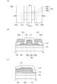
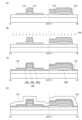
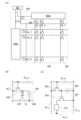
図1(A)(B)(C)に、トランジスタを有する半導体装置の一例を示す。なお、図
1(A)(B)(C)に示すトランジスタは、トップゲート構造である。<1-1. Configuration example 1 of semiconductor device>
1A to 1C show examples of a semiconductor device including a transistor. Note that the transistors shown in FIGS. 1A to 1C have a top-gate structure.
図1(A)は、トランジスタ100の上面図であり、図1(B)は図1(A)の一点鎖
線X1-X2間の断面図であり、図1(C)は図1(A)の一点鎖線Y1-Y2間の断面
図である。なお、図1(A)では、明瞭化のため、絶縁膜110などの構成要素を省略し
て図示している。なお、トランジスタの上面図においては、以降の図面においても図1(
A)と同様に、構成要素の一部を省略して図示する場合がある。また、一点鎖線X1-X
2方向をチャネル長(L)方向、一点鎖線Y1-Y2方向をチャネル幅(W)方向と呼称
する場合がある。 1A is a top view of a
As in A), some of the components may be omitted.
The two directions may be referred to as channel length (L) directions, and the direction of the dashed dotted line Y1-Y2 may be referred to as channel width (W) direction.
図1(A)(B)(C)に示すトランジスタ100は、基板102上に形成された絶縁
膜104と、絶縁膜104上の酸化物半導体膜108と、酸化物半導体膜108上の絶縁
膜110と、絶縁膜110上の酸化物半導体膜112と、絶縁膜104、酸化物半導体膜
108、及び酸化物半導体膜112上の絶縁膜116と、を有する。また、酸化物半導体
膜108は、酸化物半導体膜112が重畳し、且つ絶縁膜110と接するチャネル領域1
08iと、絶縁膜116と接するソース領域108sと、絶縁膜116と接するドレイン
領域108dと、を有する。 1A, 1B, and 1C includes an insulating
1, a
また、トランジスタ100は、絶縁膜116上の絶縁膜118と、絶縁膜116、11
8に設けられた開口部141aを介して、ソース領域108sに電気的に接続される導電
膜120aと、絶縁膜116、118に設けられた開口部141bを介して、ドレイン領
域108dに電気的に接続される導電膜120bと、を有していてもよい。 The
8, and a
なお、本明細書等において、絶縁膜104を第1の絶縁膜と、絶縁膜116を第2の絶
縁膜と、絶縁膜118を第3の絶縁膜と、それぞれ呼称する場合がある。また、絶縁膜1
10は、ゲート絶縁膜としての機能を有し、酸化物半導体膜112は、ゲート電極として
の機能を有する。また、導電膜120aは、ソース電極としての機能を有し、導電膜12
0bは、ドレイン電極としての機能を有する。 In this specification and the like, the insulating
The
0b functions as a drain electrode.
また、絶縁膜116は、窒素または水素のいずれか一方または双方を有する。絶縁膜1
16が窒素または水素のいずれか一方または双方を有する構成とすることで、酸化物半導
体膜108、及び酸化物半導体膜112に窒素または水素のいずれか一方または双方を供
給することができる。 The insulating
When the
また、酸化物半導体膜112は、絶縁膜110に酸素を供給する機能を有する。酸化物
半導体膜112が、絶縁膜110に酸素を供給する機能を有することで、絶縁膜110中
に過剰酸素を含ませることが可能となる。絶縁膜110が過剰酸素領域を有することで、
酸化物半導体膜108、より具体的にはチャネル領域108i中に当該過剰酸素を供給す
ることができる。よって、信頼性の高い半導体装置を提供することができる。 The
The excess oxygen can be supplied to the
なお、酸化物半導体膜108中に過剰酸素を供給させるためには、酸化物半導体膜10
8の下方に形成される絶縁膜104が過剰酸素を有していてもよい。ただし、絶縁膜10
4が過剰酸素を有する場合、絶縁膜104中に含まれる過剰酸素は、酸化物半導体膜10
8が有するソース領域108s、及びドレイン領域108dにも供給され得る。ソース領
域108s、及びドレイン領域108d中に過剰酸素が供給されると、ソース領域108
s、及びドレイン領域108d中の抵抗が高くなる場合がある。 In order to supply excess oxygen to the
The insulating
In the case where the insulating
When excess oxygen is supplied to the
s and the resistance in the
一方で、酸化物半導体膜108の上方に形成される絶縁膜110が過剰酸素を有する構
成とすることで、チャネル領域108iにのみ選択的に過剰酸素を供給させることが可能
となる。あるいは、チャネル領域108i、ソース領域108s、及びドレイン領域10
8dに過剰酸素を供給させたのち、ソース領域108s、及びドレイン領域108dのキ
ャリア密度を選択的に高めればよい。 On the other hand, when the insulating
After excess oxygen is supplied to the
また、酸化物半導体膜112は、絶縁膜110に酸素を供給したのち、絶縁膜116か
ら窒素または水素のいずれか一方または双方が供給されることで、キャリア密度が高くな
る。別言すると、酸化物半導体膜112は、酸化物導電体(OC:Oxide Cond
uctor)としての機能も有する。したがって、酸化物半導体膜112は、酸化物半導
体膜108よりもキャリア密度が高くなる。 In addition, the
Therefore, the
また、酸化物半導体膜108が有するソース領域108s、及びドレイン領域108d
、並びに酸化物半導体膜112は、それぞれ、酸素欠損を形成する元素を有していてもよ
い。上記酸素欠損を形成する元素としては、代表的には水素、ホウ素、炭素、窒素、フッ
素、リン、硫黄、塩素、希ガス等が挙げられる。また、希ガス元素の代表例としては、ヘ
リウム、ネオン、アルゴン、クリプトン、及びキセノン等がある。 The
and the
不純物元素が酸化物半導体膜に添加されると、酸化物半導体膜中の金属元素と酸素の結
合が切断され、酸素欠損が形成される。または、不純物元素が酸化物半導体膜に添加され
ると、酸化物半導体膜中の金属元素と結合していた酸素が不純物元素と結合し、金属元素
から酸素が脱離され、酸素欠損が形成される。これらの結果、酸化物半導体膜においてキ
ャリア密度が増加し、導電性が高くなる。 When an impurity element is added to an oxide semiconductor film, a bond between a metal element and oxygen in the oxide semiconductor film is cut, and oxygen vacancies are formed. Alternatively, when an impurity element is added to an oxide semiconductor film, oxygen that was bonded to a metal element in the oxide semiconductor film is bonded to the impurity element, and oxygen is released from the metal element, and oxygen vacancies are formed. As a result, the carrier density in the oxide semiconductor film is increased, and the conductivity is increased.
また、トランジスタ100において、絶縁膜110の側端部と、酸化物半導体膜112
の側端部とが、揃う領域を有すると好ましい。別言すると、トランジスタ100において
、絶縁膜110の上端部と、酸化物半導体膜112の下端部が概略揃う構成である。例え
ば、酸化物半導体膜112をマスクとして絶縁膜110を加工することで、上記構造とす
ることができる。 In the
In other words, in the
次に、図1(A)(B)(C)に示す半導体装置の構成要素の詳細について説明する。Next, the components of the semiconductor device shown in Figures 1(A), (B), and (C) will be described in detail.
[基板]
基板102としては、様々な基板を用いることができ、特定のものに限定されることは
ない。基板の一例としては、半導体基板(例えば単結晶基板またはシリコン基板)、SO
I基板、ガラス基板、石英基板、プラスチック基板、金属基板、ステンレス・スチル基板
、ステンレス・スチル・ホイルを有する基板、タングステン基板、タングステン・ホイル
を有する基板、可撓性基板、貼り合わせフィルム、繊維状の材料を含む紙、または基材フ
ィルムなどがある。ガラス基板の一例としては、バリウムホウケイ酸ガラス、アルミノホ
ウケイ酸ガラス、またはソーダライムガラスなどがある。可撓性基板、貼り合わせフィル
ム、基材フィルムなどの一例としては、以下のものがあげられる。例えば、ポリエチレン
テレフタレート(PET)、ポリエチレンナフタレート(PEN)、ポリエーテルサルフ
ォン(PES)に代表されるプラスチックがある。または、一例としては、アクリル等の
合成樹脂などがある。または、一例としては、ポリプロピレン、ポリエステル、ポリフッ
化ビニル、ポリ塩化ビニルなどがある。または、一例としては、ポリアミド、ポリイミド
、アラミド、エポキシ、無機蒸着フィルム、または紙類などがある。特に、半導体基板、
単結晶基板、またはSOI基板などを用いてトランジスタを製造することによって、特性
、サイズ、または形状などのばらつきが少なく、電流能力が高く、サイズの小さいトラン
ジスタを製造することができる。このようなトランジスタによって回路を構成すると、回
路の低消費電力化、または回路の高集積化を図ることができる。[substrate]
Various substrates can be used as the
Examples of the substrate include an I substrate, a glass substrate, a quartz substrate, a plastic substrate, a metal substrate, a stainless steel substrate, a substrate having a stainless steel foil, a tungsten substrate, a substrate having a tungsten foil, a flexible substrate, a laminated film, a paper containing a fibrous material, or a base film. Examples of the glass substrate include barium borosilicate glass, aluminoborosilicate glass, or soda lime glass. Examples of the flexible substrate, the laminated film, the base film, or the like include the following. For example, there are plastics represented by polyethylene terephthalate (PET), polyethylene naphthalate (PEN), and polyethersulfone (PES). As another example, there are synthetic resins such as acrylic. As another example, there are polypropylene, polyester, polyvinyl fluoride, and polyvinyl chloride. As another example, there are polyamide, polyimide, aramid, epoxy, inorganic vapor deposition films, and papers. In particular, semiconductor substrates,
By manufacturing a transistor using a single crystal substrate, an SOI substrate, etc., it is possible to manufacture a transistor that has a small size, high current capability, and little variation in characteristics, size, shape, etc. By configuring a circuit using such transistors, it is possible to reduce the power consumption of the circuit or to increase the integration density of the circuit.
また、基板102として、可撓性基板を用い、可撓性基板上に直接、トランジスタを形
成してもよい。または、基板102とトランジスタの間に剥離層を設けてもよい。剥離層
は、その上に半導体装置を一部あるいは全部完成させた後、基板102より分離し、他の
基板に転載するのに用いることができる。その際、トランジスタを耐熱性の劣る基板や可
撓性の基板にも転載できる。なお、上述の剥離層には、例えば、タングステン膜と酸化シ
リコン膜との無機膜の積層構造の構成、または基板上にポリイミド等の有機樹脂膜が形成
された構成等を用いることができる。 Alternatively, a flexible substrate may be used as the
トランジスタが転載される基板の一例としては、上述したトランジスタを形成すること
が可能な基板に加え、紙基板、セロファン基板、アラミドフィルム基板、ポリイミドフィ
ルム基板、石材基板、木材基板、布基板(天然繊維(絹、綿、麻)、合成繊維(ナイロン
、ポリウレタン、ポリエステル)若しくは再生繊維(アセテート、キュプラ、レーヨン、
再生ポリエステル)などを含む)、皮革基板、またはゴム基板などがある。これらの基板
を用いることにより、特性のよいトランジスタの形成、消費電力の小さいトランジスタの
形成、壊れにくい装置の製造、耐熱性の付与、軽量化、または薄型化を図ることができる
。 Examples of the substrate on which the transistors are transferred include, in addition to the substrates on which the above-mentioned transistors can be formed, paper substrates, cellophane substrates, aramid film substrates, polyimide film substrates, stone substrates, wood substrates, cloth substrates (natural fibers (silk, cotton, hemp), synthetic fibers (nylon, polyurethane, polyester) or regenerated fibers (acetate, cupra, rayon,
The substrates include substrates made of materials such as recycled polyester, leather, and rubber. By using these substrates, it is possible to form transistors with good characteristics, transistors with low power consumption, and to manufacture devices that are durable, heat resistant, lightweight, and thin.
[第1の絶縁膜]
絶縁膜104としては、スパッタリング法、CVD法、蒸着法、パルスレーザー堆積(
PLD)法、印刷法、塗布法等を適宜用いて形成することができる。また、絶縁膜104
としては、例えば、酸化物絶縁膜または窒化物絶縁膜を単層または積層して形成すること
ができる。なお、酸化物半導体膜108との界面特性を向上させるため、絶縁膜104に
おいて少なくとも酸化物半導体膜108と接する領域は酸化物絶縁膜で形成することが好
ましい。また、絶縁膜104として加熱により酸素を放出する酸化物絶縁膜を用いること
で、加熱処理により絶縁膜104に含まれる酸素を、酸化物半導体膜108に移動させる
ことが可能である。[First insulating film]
The insulating
The insulating
For example, the insulating
絶縁膜104の厚さは、50nm以上、または100nm以上3000nm以下、また
は200nm以上1000nm以下とすることができる。絶縁膜104を厚くすることで
、絶縁膜104の酸素放出量を増加させることができると共に、絶縁膜104と酸化物半
導体膜108との界面における界面準位、並びに酸化物半導体膜108のチャネル領域1
08iに含まれる酸素欠損を低減することが可能である。 The thickness of the insulating
It is possible to reduce the oxygen vacancies contained in 08i.
絶縁膜104として、例えば酸化シリコン、酸化窒化シリコン、窒化酸化シリコン、窒
化シリコン、酸化アルミニウム、酸化ハフニウム、酸化ガリウムまたはGa-Zn酸化物
などを用いればよく、単層または積層で設けることができる。本実施の形態では、絶縁膜
104として、窒化シリコン膜と、酸化窒化シリコン膜との積層構造を用いる。このよう
に、絶縁膜104を積層構造として、下層側に窒化シリコン膜を用い、上層側に酸化窒化
シリコン膜を用いることで、酸化物半導体膜108中に効率よく酸素を導入することがで
きる。 The insulating
[酸化物半導体膜]
酸化物半導体膜108及び酸化物半導体膜112のいずれか一方または双方は、In-
M-Zn酸化物(MはAl、Ga、Y、またはSn)等の金属酸化物で形成される。また
、酸化物半導体膜108及び酸化物半導体膜112として、In-Ga酸化物、In-Z
n酸化物を用いてもよい。とくに、酸化物半導体膜108と、酸化物半導体膜112とは
、同じ構成元素からなる金属酸化物で形成されると、製造コストを低減できるため好まし
い。[Oxide Semiconductor Film]
One or both of the
The
In particular, it is preferable that the
なお、酸化物半導体膜108及び酸化物半導体膜112がIn-M-Zn酸化物の場合
、InとMの原子数比率は、In及びMの和を100atomic%としたときInが2
5atomic%より高く、Mが75atomic%未満、またはInが34atomi
c%より高く、Mが66atomic%未満とする。 Note that in the case where the
5 atomic % or more, M is less than 75 atomic %, or In is 34 atomic % or more
c%, and M is less than 66 atomic %.
酸化物半導体膜108及び酸化物半導体膜112は、エネルギーギャップが2eV以上
、または2.5eV以上、または3eV以上であると好ましい。 The
酸化物半導体膜108の厚さは、3nm以上200nm以下、好ましくは3nm以上1
00nm以下、さらに好ましくは3nm以上60nm以下である。また、酸化物半導体膜
112の厚さは、5nm以上500nm以下、好ましくは10nm以上300nm以下、
さらに好ましくは20nm以上100nm以下である。 The thickness of the
The thickness of the
More preferably, it is 20 nm or more and 100 nm or less.
酸化物半導体膜108、及び酸化物半導体膜112がIn-M-Zn酸化物の場合、I
n-M-Zn酸化物を成膜するために用いるスパッタリングターゲットの金属元素の原子
数比は、In≧M、Zn≧Mを満たすことが好ましい。このようなスパッタリングターゲ
ットの金属元素の原子数比として、In:M:Zn=1:1:1、In:M:Zn=1:
1:1.2、In:M:Zn=2:1:1.5、In:M:Zn=2:1:2.3、In
:M:Zn=2:1:3、In:M:Zn=3:1:2、In:M:Zn=4:2:4.
1、In:M:Zn=5:1:7等が好ましい。なお、成膜される酸化物半導体膜108
、及び酸化物半導体膜112の原子数比はそれぞれ、上記のスパッタリングターゲットに
含まれる金属元素の原子数比のプラスマイナス40%程度変動することがある。例えば、
スパッタリングターゲットとして、原子数比がIn:Ga:Zn=4:2:4.1を用い
る場合、成膜される酸化物半導体膜108、及び酸化物半導体膜112の原子数比は、I
n:Ga:Zn=4:2:3近傍となる場合がある。 When the
The atomic ratio of metal elements in a sputtering target used to form a film of n-M-Zn oxide preferably satisfies In≧M and Zn≧M. The atomic ratio of metal elements in such a sputtering target is preferably In:M:Zn=1:1:1, In:M:Zn=1:
1:1.2, In:M:Zn=2:1:1.5, In:M:Zn=2:1:2.3, In
:M:Zn=2:1:3, In:M:Zn=3:1:2, In:M:Zn=4:2:4.
In:M:Zn=5:1:7, for example.
and the atomic ratio of the
When a sputtering target having an atomic ratio of In:Ga:Zn=4:2:4.1 is used, the atomic ratio of the
In some cases, the n:Ga:Zn ratio is approximately 4:2:3.
また、酸化物半導体膜108において、第14族元素の一つであるシリコンや炭素が含
まれると、酸素欠損が増加し、n型となる場合がある。このため、酸化物半導体膜108
、特にチャネル領域108iにおいて、シリコンあるいは炭素の濃度(二次イオン質量分
析法により得られる濃度)を、2×10¹⁸atoms/cm3以下、または2×101
7atoms/cm3以下とすることができる。この結果、トランジスタは、しきい値電
圧がプラスとなる電気特性(ノーマリーオフ特性ともいう。)を有する。 In addition, when the
In particular, in the
7 atoms/cm3 or less. As a result, the transistor has electrical characteristics in which the threshold voltage is positive (also referred to as normally-off characteristics).
また、チャネル領域108iにおいて、二次イオン質量分析法により得られるアルカリ
金属またはアルカリ土類金属の濃度を、1×10¹⁸atoms/cm3以下、または2
×1016atoms/cm3以下とすることができる。アルカリ金属及びアルカリ土類
金属は、酸化物半導体と結合するとキャリアを生成する場合があり、トランジスタのオフ
電流が増大してしまうことがある。このため、チャネル領域108iのアルカリ金属また
はアルカリ土類金属の濃度を低減することが好ましい。この結果、トランジスタは、しき
い値電圧がプラスとなる電気特性(ノーマリーオフ特性ともいう。)を有する。 In the
×1016 atoms/cm3 or less. When an alkali metal or an alkaline earth metal is bonded to an oxide semiconductor, carriers may be generated, which may increase the off-state current of the transistor. For this reason, it is preferable to reduce the concentration of the alkali metal or alkaline earth metal in the
また、チャネル領域108iに窒素が含まれていると、キャリアである電子が生じ、キ
ャリア密度が増加し、n型となる場合がある。この結果、窒素が含まれている酸化物半導
体膜を用いたトランジスタはノーマリーオン特性となりやすい。従って、チャネル領域1
08iにおいて、窒素はできる限り低減されていることが好ましい。例えば、二次イオン
質量分析法により得られる窒素濃度を、5×10¹⁸atoms/cm3以下とすればよ
い。 Furthermore, when nitrogen is contained in the
In the case of 08i, it is preferable that the nitrogen content is reduced as much as possible. For example, the nitrogen concentration obtained by secondary ion mass spectrometry may be reduced to 5×10¹⁸ atoms/cm3 or less.
また、チャネル領域108iにおいて、不純物元素を低減することで、酸化物半導体膜
のキャリア密度を低減することができる。このため、チャネル領域108iにおいては、
キャリア密度を1×10¹⁷個/cm3以下、または1×1015個/cm3以下、また
は1×10¹³個/cm3以下、または1×1011個/cm3以下とすることができる
。 Furthermore, by reducing the impurity elements in the
The carrier density can be 1×10¹⁷ particles/cm3 or less, or 1×10¹⁵ particles/cm3 or less, or 1×10¹³ particles/cm3 or less, or 1×10¹¹ particles/cm3 or less.
チャネル領域108iとして、不純物濃度が低く、欠陥準位密度の低い酸化物半導体膜
を用いることで、さらに優れた電気特性を有するトランジスタを作製することができる。
ここでは、不純物濃度が低く、欠陥準位密度の低い(酸素欠損の少ない)ことを高純度真
性または実質的に高純度真性と呼ぶ。あるいは、真性、または実質的に真性と呼ぶ。高純
度真性または実質的に高純度真性である酸化物半導体は、キャリア発生源が少ないため、
キャリア密度を低くすることができる場合がある。従って、当該酸化物半導体膜にチャネ
ル領域が形成されるトランジスタは、しきい値電圧がプラスとなる電気特性(ノーマリー
オフ特性ともいう。)になりやすい。また、高純度真性または実質的に高純度真性である
酸化物半導体膜は、欠陥準位密度が低いため、トラップ準位密度も低くなる場合がある。
また、高純度真性または実質的に高純度真性である酸化物半導体膜は、オフ電流が著しく
小さい特性を得ることができる。従って、当該酸化物半導体膜にチャネル領域が形成され
るトランジスタは、電気特性の変動が小さく、信頼性の高いトランジスタとなる場合があ
る。 When an oxide semiconductor film with a low impurity concentration and a low density of defect states is used for the
Here, an oxide semiconductor having a low impurity concentration and a low density of defect states (few oxygen vacancies) is referred to as being highly pure intrinsic or substantially highly pure intrinsic. Alternatively, it is referred to as being intrinsic or substantially intrinsic. A highly pure intrinsic or substantially highly pure intrinsic oxide semiconductor has a small number of carrier generation sources,
The carrier density can be reduced in some cases. Therefore, a transistor in which a channel region is formed in the oxide semiconductor film tends to have electrical characteristics in which the threshold voltage is positive (also referred to as normally-off characteristics). In addition, a highly-purified intrinsic or substantially highly-purified intrinsic oxide semiconductor film has a low density of defect states, and therefore the density of trap states can also be reduced in some cases.
In addition, a highly-purified intrinsic or substantially highly-purified intrinsic oxide semiconductor film can have an extremely small off-state current. Therefore, a transistor in which a channel region is formed in the oxide semiconductor film has small fluctuation in electrical characteristics and can be a highly reliable transistor in some cases.
一方で、ソース領域108s、ドレイン領域108d、及び酸化物半導体膜112は、
絶縁膜116と接する。ソース領域108s、ドレイン領域108d、及び酸化物半導体
膜112が絶縁膜116と接することで、絶縁膜116からソース領域108s、ドレイ
ン領域108d、及び酸化物半導体膜112に水素及び窒素のいずれか一方または双方が
添加されるため、キャリア密度が高くなる。 On the other hand, the
The
また、酸化物半導体膜108、及び酸化物半導体膜112のいずれか一方または双方は
、非単結晶構造でもよい。非単結晶構造は、例えば、後述するCAAC-OS(C Ax
is Aligned Crystalline Oxide Semiconduct
or)、多結晶構造、後述する微結晶構造、または非晶質構造を含む。非単結晶構造にお
いて、非晶質構造は最も欠陥準位密度が高く、CAAC-OSは最も欠陥準位密度が低い
。 Either or both of the
is Aligned Crystalline Oxide Semiconductor
Among non-single crystal structures, the amorphous structure has the highest density of defect states, and the CAAC-OS has the lowest density of defect states.
なお、酸化物半導体膜108が、非晶質構造の領域、微結晶構造の領域、多結晶構造の
領域、CAAC-OSの領域、及び単結晶構造の領域の二種以上を有する単層膜、あるい
はこの膜が積層された構造であってもよい。また、酸化物半導体膜112が、非晶質構造
の領域、微結晶構造の領域、多結晶構造の領域、CAAC-OSの領域、及び単結晶構造
の領域の二種以上を有する単層膜、あるいはこの膜が積層された構造であってもよい。 Note that the
なお、酸化物半導体膜108において、チャネル領域108iと、ソース領域108s
及びドレイン領域108dとの結晶性が異なる場合がある。具体的には、酸化物半導体膜
108において、チャネル領域108iよりもソース領域108s及びドレイン領域10
8dの方が、結晶性が低い場合がある。これは、ソース領域108s及びドレイン領域1
08dに不純物元素が添加された際に、ソース領域108s及びドレイン領域108dに
ダメージが入ってしまい、結晶性が低下するためである。 Note that in the
Specifically, in the
The
This is because, when an impurity element is added to the
[ゲート絶縁膜として機能する絶縁膜]
絶縁膜110は、酸化物絶縁膜または窒化物絶縁膜を単層または積層して形成すること
ができる。なお、酸化物半導体膜108との界面特性を向上させるため、絶縁膜110に
おいて少なくとも酸化物半導体膜108と接する領域は酸化物絶縁膜を用いて形成するこ
とが好ましい。絶縁膜110として、例えば酸化シリコン、酸化窒化シリコン、窒化酸化
シリコン、窒化シリコン、酸化アルミニウム、酸化ハフニウム、酸化ガリウムまたはGa
-Zn酸化物などを用いればよく、単層または積層で設けることができる。[Insulating film functioning as a gate insulating film]
The insulating
A -Zn oxide or the like may be used, and the layer may be formed as a single layer or a multilayer.
また、絶縁膜110として、酸素、水素、水等のブロッキング効果を有する絶縁膜を設
けることで、酸化物半導体膜108からの酸素の外部への拡散と、外部から酸化物半導体
膜108への水素、水等の侵入を防ぐことができる。酸素、水素、水等のブロッキング効
果を有する絶縁膜としては、酸化アルミニウム膜、酸化窒化アルミニウム膜、酸化ガリウ
ム膜、酸化窒化ガリウム膜、酸化イットリウム膜、酸化窒化イットリウム膜、酸化ハフニ
ウム膜、酸化窒化ハフニウム膜等がある。 Furthermore, by providing an insulating film having a blocking effect against oxygen, hydrogen, water, and the like as the insulating
また、絶縁膜110として、ハフニウムシリケート(HfSiOx)、窒素が添加され
たハフニウムシリケート(HfSixOyNz)、窒素が添加されたハフニウムアルミネ
ート(HfAlxOyNz)、酸化ハフニウム、酸化イットリウムなどのhigh-k材
料を用いることでトランジスタのゲートリークを低減できる。 Furthermore, by using a high-k material such as hafnium silicate (HfSiOx ), hafnium silicate doped with nitrogen (HfSix Oy Nz ), hafnium aluminate doped with nitrogen (HfAlx Oy Nz ), hafnium oxide, or yttrium oxide for the insulating
また、絶縁膜110として、加熱により酸素を放出する酸化物絶縁膜を用いることで、
加熱処理により絶縁膜110に含まれる酸素を、酸化物半導体膜108に移動させること
が可能である。 In addition, by using an oxide insulating film that releases oxygen by heating as the insulating
By the heat treatment, oxygen contained in the insulating
絶縁膜110の厚さは、5nm以上400nm以下、または5nm以上300nm以下
、または10nm以上250nm以下とすることができる。 The thickness of the insulating
[第2の絶縁膜]
絶縁膜116は、窒素または水素のいずれか一方または双方を有する。絶縁膜116と
しては、例えば、窒化物絶縁膜が挙げられる。該窒化物絶縁膜としては、窒化シリコン、
窒化酸化シリコン、窒化アルミニウム、窒化酸化アルミニウム等を用いて形成することが
できる。絶縁膜116に含まれる水素濃度は、1×10²²atoms/cm3以上であ
ると好ましい。また、絶縁膜116は、酸化物半導体膜108のソース領域108s、及
びドレイン領域108dと接する。また、絶縁膜116は、酸化物半導体膜112と接す
る。したがって、絶縁膜116と接するソース領域108s、ドレイン領域108d、及
び酸化物半導体膜112中の水素濃度が高くなり、ソース領域108s、ドレイン領域1
08d、及び酸化物半導体膜112のキャリア密度を高めることができる。なお、ソース
領域108s、ドレイン領域108d、及び酸化物半導体膜112としては、それぞれ絶
縁膜116と接することで、膜中の水素濃度が同じ領域を有する場合がある。[Second insulating film]
The insulating
The insulating
This can increase the carrier density in the
[第3の絶縁膜]
絶縁膜118としては、酸化物絶縁膜または窒化物絶縁膜を単層または積層して形成す
ることができる。絶縁膜118として、例えば酸化シリコン、酸化窒化シリコン、窒化酸
化シリコン、窒化シリコン、酸化アルミニウム、酸化ハフニウム、酸化ガリウムまたはG
a-Zn酸化物などを用いればよく、単層または積層で設けることができる。[Third insulating film]
The insulating
A-Zn oxide or the like may be used, and the layer may be formed as a single layer or a multilayer.
また、絶縁膜118としては、外部からの水素、水等のバリア膜として機能する膜であ
ることが好ましい。 The insulating
絶縁膜118の厚さは、30nm以上500nm以下、または100nm以上400n
m以下とすることができる。 The thickness of the insulating
m or less.
[導電膜]
導電膜120a、120bとしては、スパッタリング法、真空蒸着法、パルスレーザー
堆積(PLD)法、熱CVD法等を用いて形成することができる。また、導電膜120a
、120bとしては、例えば、アルミニウム、クロム、銅、タンタル、チタン、モリブデ
ン、ニッケル、鉄、コバルト、タングステンから選ばれた金属元素、または上述した金属
元素を成分とする合金か、上述した金属元素を組み合わせた合金等を用いて形成すること
ができる。また、マンガン、ジルコニウムのいずれか一または複数から選択された金属元
素を用いてもよい。また、導電膜120a、120bは、単層構造でも、二層以上の積層
構造としてもよい。例えば、シリコンを含むアルミニウム膜の単層構造、マンガンを含む
銅膜の単層構造、アルミニウム膜上にチタン膜を積層する二層構造、窒化チタン膜上にチ
タン膜を積層する二層構造、窒化チタン膜上にタングステン膜を積層する二層構造、窒化
タンタル膜または窒化タングステン膜上にタングステン膜を積層する二層構造、マンガン
を含む銅膜上に銅膜を積層する二層構造、チタン膜上に銅膜を積層する二層構造、チタン
膜と、そのチタン膜上にアルミニウム膜を積層し、さらにその上にチタン膜を形成する三
層構造、マンガンを含む銅膜上に銅膜を積層し、さらにその上にマンガンを含む銅膜を形
成する三層構造等がある。また、アルミニウムに、チタン、タンタル、タングステン、モ
リブデン、クロム、ネオジム、スカンジウムから選ばれた一または複数を組み合わせた合
金膜、もしくは窒化膜を用いてもよい。[Conductive film]
The
The
また、導電膜120a、120bは、インジウム錫酸化物(Indium Tin O
xide:ITO)、酸化タングステンを含むインジウム酸化物、酸化タングステンを含
むインジウム亜鉛酸化物、酸化チタンを含むインジウム酸化物、酸化チタンを含むインジ
ウム錫酸化物、インジウム亜鉛酸化物、シリコンを含むインジウム錫酸化物(In-Sn
-Si酸化物:ITSOともいう)等の透光性を有する導電性材料を適用することもでき
る。また、上記透光性を有する導電性材料と、上記金属元素の積層構造とすることもでき
る。 The
xide: ITO), indium oxide containing tungsten oxide, indium zinc oxide containing tungsten oxide, indium oxide containing titanium oxide, indium tin oxide containing titanium oxide, indium zinc oxide, indium tin oxide containing silicon (In-Sn
A light-transmitting conductive material such as -Si oxide (also referred to as ITSO) can also be used. A stacked structure of the above light-transmitting conductive material and the above metal element can also be used.
導電膜120a、120bの厚さとしては、30nm以上500nm以下、または10
0nm以上400nm以下とすることができる。 The thickness of the
The thickness can be set to 0 nm or more and 400 nm or less.
<1-2.半導体装置の構成例2>
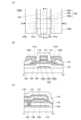
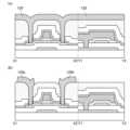
次に、図1(A)(B)(C)に示す半導体装置と異なる構成について、図2(A)(
B)(C)を用いて説明する。<1-2. Configuration example 2 of semiconductor device>
Next, regarding a semiconductor device having a structure different from that shown in FIG.
B) (C) will be used to explain.
図2(A)は、トランジスタ150の上面図であり、図2(B)は図2(A)の一点鎖
線X1-X2間の断面図であり、図2(C)は図2(A)の一点鎖線Y1-Y2間の断面
図である。 2A is a top view of a
図2(A)(B)(C)に示すトランジスタ150は、基板102上に形成された絶縁
膜104と、絶縁膜104上の酸化物半導体膜108と、酸化物半導体膜108上の絶縁
膜110と、絶縁膜110上の酸化物半導体膜112と、酸化物半導体膜112上の導電
膜114と、絶縁膜104、酸化物半導体膜108、及び導電膜114上の絶縁膜116
と、を有する。また、酸化物半導体膜108は、酸化物半導体膜112が重畳し、且つ絶
縁膜110と接するチャネル領域108iと、絶縁膜116と接するソース領域108s
と、絶縁膜116と接するドレイン領域108dと、を有する。 A
The
and a
また、トランジスタ150は、絶縁膜116上の絶縁膜118と、絶縁膜116、11
8に設けられた開口部141aを介して、ソース領域108sに電気的に接続される導電
膜120aと、絶縁膜116、118に設けられた開口部141bを介して、ドレイン領
域108dに電気的に接続される導電膜120bと、を有していてもよい。 The
8, and a
なお、トランジスタ150においては、酸化物半導体膜112と、導電膜114とがゲ
ート電極としての機能を有する。また、導電膜114は、酸化物半導体膜112をn型に
する機能を有する。導電膜114が酸化物半導体膜112をn型にする機能を有する構成
とすることで、酸化物半導体膜112は、ゲート電極の一部として機能する。 Note that in the
また、絶縁膜116は、窒素または水素のいずれか一方または双方を有する。絶縁膜1
16が窒素または水素のいずれか一方または双方を有する構成とすることで、ソース領域
108s及びドレイン領域108dに窒素または水素のいずれか一方または双方を供給す
ることができる。 The insulating
By using a structure in which the second insulating
また、酸化物半導体膜112は、絶縁膜110に酸素を供給する機能を有する。酸化物
半導体膜112が、絶縁膜110に酸素を供給する機能を有することで、絶縁膜110中
に過剰酸素を含ませることが可能となる。絶縁膜110が過剰酸素領域を有することで、
チャネル領域108i中に当該過剰酸素を供給することができる。よって、信頼性の高い
半導体装置を提供することができる。 The
The excess oxygen can be supplied into the
なお、酸化物半導体膜112は、絶縁膜110に酸素を供給したのち、キャリア密度が
高くなる。また、酸化物半導体膜112が導電膜114と接することによって、導電膜1
14の構成元素が酸化物半導体膜112へ拡散し、キャリア密度が高くなる場合がある。
別言すると、酸化物半導体膜112は、酸化物導電体(OC)としての機能も有する。し
たがって、製造工程を増加させることが無く、酸化物半導体膜112をゲート電極の一部
として機能させることが可能となる。 Note that the
A constituent element of the
In other words, the
導電膜114としては、先に記載の導電膜120a、120bと同様の形成方法、及び
同様の材料を用いて形成される。特に導電膜114としては、チタン、銅、またはタング
ステンを用いて、スパッタリング法を用いて形成すると好適である。導電膜114にチタ
ン、銅、またはタングステンを用いることで、導電膜114と接する酸化物半導体膜11
2の導電性を向上させることができる。また、導電膜114を積層構造としてもよい。当
該積層構造としては、例えば、マンガンを含む銅膜上に銅膜を有する構造、または、タン
グステン膜上にアルミニウム膜を有する構造とすればよい。 The
The
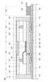
<1-3.半導体装置の構成例3>
次に、図1(A)(B)(C)に示す半導体装置と異なる構成について、図3(A)(
B)(C)を用いて説明する。<1-3. Configuration example 3 of semiconductor device>
Next, regarding a semiconductor device having a structure different from that shown in FIG.
B) (C) will be used to explain.
図3(A)は、トランジスタ100Aの上面図であり、図3(B)は図3(A)の一点
鎖線X1-X2間の断面図であり、図3(C)は図3(A)の一点鎖線Y1-Y2間の断
面図である。 3A is a top view of a
図3(A)(B)(C)に示すトランジスタ100Aは、基板102上に形成された導
電膜106と、導電膜106上の絶縁膜104と、絶縁膜104上の酸化物半導体膜10
8と、酸化物半導体膜108上の絶縁膜110と、絶縁膜110上の酸化物半導体膜11
2と、絶縁膜104、酸化物半導体膜108、及び酸化物半導体膜112上の絶縁膜11
6と、を有する。また、酸化物半導体膜108は、絶縁膜110と接するチャネル領域1
08iと、絶縁膜116と接するソース領域108sと、絶縁膜116と接するドレイン
領域108dと、を有する。 A
8, an insulating
2, and the insulating
The
1, a
トランジスタ100Aは、先に示すトランジスタ100の構成に加え、導電膜106と
、開口部143と、を有する。 The
なお、開口部143は、絶縁膜104、110に設けられる。また、導電膜106は、
開口部143を介して、酸化物半導体膜112と、電気的に接続される。よって、導電膜
106と酸化物半導体膜112には、同じ電位が与えられる。また、開口部143を設け
ずに、導電膜106と、酸化物半導体膜112と、に異なる電位を与えてもよい。 The
The
なお、導電膜106は、第1のゲート電極(ボトムゲート電極ともいう)としての機能
を有し、酸化物半導体膜112は、第2のゲート電極(トップゲート電極ともいう)とし
ての機能を有する。また、絶縁膜104は、第1のゲート絶縁膜としての機能を有し、絶
縁膜110は、第2のゲート絶縁膜としての機能を有する。 Note that the
このように、図3(A)(B)(C)に示すトランジスタ100Aは、先に説明したト
ランジスタ100と異なり、酸化物半導体膜108の上下にゲート電極として機能する導
電膜および酸化物半導体膜を有する構造である。トランジスタ100Aに示すように、本
発明の一態様の半導体装置には、2つ以上のゲート電極を設けてもよい。 3A, 3B, and 3C has a structure including a conductive film and an oxide semiconductor film functioning as a gate electrode above and below the
また、図3(C)に示すように、酸化物半導体膜108は、第1のゲート電極として機
能する導電膜106と、第2のゲート電極として機能する酸化物半導体膜112のそれぞ
れと対向するように位置し、2つのゲート電極として機能する導電膜および酸化物半導体
膜に挟まれている。 As shown in FIG. 3C , the
また、酸化物半導体膜112のチャネル幅方向の長さは、酸化物半導体膜108のチャ
ネル幅方向の長さよりも長く、酸化物半導体膜108のチャネル幅方向全体は、絶縁膜1
10を介して酸化物半導体膜112に覆われている。また、酸化物半導体膜112と導電
膜106とは、絶縁膜104及び絶縁膜110に設けられる開口部143において接続さ
れるため、酸化物半導体膜108のチャネル幅方向の側面の一方は、酸化物半導体膜11
2と対向している。 In addition, the length of the
Since the
It is opposite to 2.
別言すると、トランジスタ100Aのチャネル幅方向において、導電膜106及び酸化
物半導体膜112は、絶縁膜104及び絶縁膜110に設けられる開口部143において
接続すると共に、絶縁膜104及び絶縁膜110を介して酸化物半導体膜108を取り囲
む構成である。 In other words, in the channel width direction of the
このような構成を有することで、トランジスタ100Aに含まれる酸化物半導体膜10
8を、第1のゲート電極として機能する導電膜106及び第2のゲート電極として機能す
る酸化物半導体膜112の電界によって電気的に取り囲むことができる。トランジスタ1
00Aのように、第1のゲート電極及び第2のゲート電極の電界によって、チャネル領域
が形成される酸化物半導体膜108を電気的に取り囲むトランジスタのデバイス構造をS
urrounded channel(S-channel)構造と呼ぶことができる。 With such a configuration, the
The
00A, the device structure of the transistor in which the
This can be called an S-channel (surrounded channel) structure.
トランジスタ100Aは、S-channel構造を有するため、導電膜106または
酸化物半導体膜112によってチャネルを誘起させるための電界を効果的に酸化物半導体
膜108に印加することができるため、トランジスタ100Aの電流駆動能力が向上し、
高いオン電流特性を得ることが可能となる。また、オン電流を高くすることが可能である
ため、トランジスタ100Aを微細化することが可能となる。また、酸化物半導体膜10
8は、導電膜106、及び酸化物半導体膜112によって取り囲まれた構造を有するため
、酸化物半導体膜108の機械的強度を高めることができる。 Since the
It is possible to obtain high on-state current characteristics. In addition, since the on-state current can be increased, the
Since the
なお、トランジスタ100Aのチャネル幅方向において、酸化物半導体膜108の開口
部143が形成されていない側面に、開口部143と異なる開口部を形成してもよい。 Note that an opening different from the
また、トランジスタ100Aに示すように、トランジスタが、半導体膜を間に挟んで存
在する一対のゲート電極を有している場合、一方のゲート電極には信号Aが、他方のゲー
ト電極には固定電位Vbが与えられてもよい。また、一方のゲート電極には信号Aが、他
方のゲート電極には信号Bが与えられてもよい。また、一方のゲート電極には固定電位V
aが、他方のゲート電極には固定電位Vbが与えられてもよい。 In addition, as shown in the
a, and a fixed potential Vb may be applied to the other gate electrode.
信号Aは、例えば、導通状態または非導通状態を制御するための信号である。信号Aは
、電位V1、または電位V2(V1>V2とする)の2種類の電位をとるデジタル信号で
あってもよい。例えば、電位V1を高電源電位とし、電位V2を低電源電位とすることが
できる。信号Aは、アナログ信号であってもよい。 The signal A is, for example, a signal for controlling a conductive state or a non-conductive state. The signal A may be a digital signal having two types of potentials, a potential V1 or a potential V2 (V1>V2). For example, the potential V1 may be a high power supply potential, and the potential V2 may be a low power supply potential. The signal A may be an analog signal.
固定電位Vbは、例えば、トランジスタのしきい値電圧VthAを制御するための電位
である。固定電位Vbは、電位V1、または電位V2であってもよい。固定電位Vbは、
電位V1、または電位V2と異なる電位であってもよい。固定電位Vbを低くすることで
、しきい値電圧VthAを高くできる場合がある。その結果、ゲートーソース間電圧Vg
sが0Vのときのドレイン電流を低減し、トランジスタを有する回路のリーク電流を低減
できる場合がある。例えば、固定電位Vbを低電源電位よりも低くしてもよい。固定電位
Vbを高くすることで、しきい値電圧VthAを低くできる場合がある。その結果、ゲー
トーソース間電圧VgsがVDDのときのドレイン電流を向上させ、トランジスタを有す
る回路の動作速度を向上できる場合がある。例えば、固定電位Vbを低電源電位よりも高
くしてもよい。 The fixed potential Vb is, for example, a potential for controlling the threshold voltage VthA of the transistor. The fixed potential Vb may be a potential V1 or a potential V2. The fixed potential Vb is,
The fixed potential Vb may be different from the potential V1 or the potential V2. By lowering the fixed potential Vb, the threshold voltage VthA may be increased. As a result, the gate-source voltage Vg
It may be possible to reduce the drain current when s is 0V, and reduce the leakage current of a circuit having a transistor. For example, the fixed potential Vb may be lower than the low power supply potential. It may be possible to lower the threshold voltage VthA by increasing the fixed potential Vb. As a result, it may be possible to improve the drain current when the gate-source voltage Vgs is VDD, and to improve the operating speed of a circuit having a transistor. For example, the fixed potential Vb may be higher than the low power supply potential.
信号Bは、例えば、導通状態または非導通状態を制御するための信号である。信号Bは
、電位V3、または電位V4(V3>V4とする)の2種類の電位をとるデジタル信号で
あってもよい。例えば、電位V3を高電源電位とし、電位V4を低電源電位とすることが
できる。信号Bは、アナログ信号であってもよい。 The signal B is, for example, a signal for controlling a conductive state or a non-conductive state. The signal B may be a digital signal having two types of potentials, a potential V3 or a potential V4 (V3>V4). For example, the potential V3 may be a high power supply potential, and the potential V4 may be a low power supply potential. The signal B may be an analog signal.
信号Aと信号Bが共にデジタル信号である場合、信号Bは、信号Aと同じデジタル値を
持つ信号であってもよい。この場合、トランジスタのオン電流を向上し、トランジスタを
有する回路の動作速度を向上できる場合がある。このとき、信号Aにおける電位V1及び
電位V2は、信号Bにおける電位V3及び電位V4と、異なっていても良い。例えば、信
号Bが入力されるゲートに対応するゲート絶縁膜が、信号Aが入力されるゲートに対応す
るゲート絶縁膜よりも厚い場合、信号Bの電位振幅(V3-V4)を、信号Aの電位振幅
(V1-V2)より大きくしても良い。そうすることで、トランジスタの導通状態または
非導通状態に対して、信号Aが与える影響と、信号Bが与える影響と、を同程度とするこ
とができる場合がある。 When both the signal A and the signal B are digital signals, the signal B may be a signal having the same digital value as the signal A. In this case, the on-current of the transistor may be improved, and the operating speed of the circuit having the transistor may be improved. In this case, the potentials V1 and V2 of the signal A may be different from the potentials V3 and V4 of the signal B. For example, when the gate insulating film corresponding to the gate to which the signal B is input is thicker than the gate insulating film corresponding to the gate to which the signal A is input, the potential amplitude (V3-V4) of the signal B may be made larger than the potential amplitude (V1-V2) of the signal A. By doing so, it may be possible to make the influence of the signal A and the influence of the signal B on the conductive or non-conductive state of the transistor comparable.
信号Aと信号Bが共にデジタル信号である場合、信号Bは、信号Aと異なるデジタル値
を持つ信号であってもよい。この場合、トランジスタの制御を信号Aと信号Bによって別
々に行うことができ、より高い機能を実現できる場合がある。例えば、トランジスタがn
チャネル型である場合、信号Aが電位V1であり、かつ、信号Bが電位V3である場合の
み導通状態となる場合や、信号Aが電位V2であり、かつ、信号Bが電位V4である場合
のみ非導通状態となる場合には、一つのトランジスタでNAND回路やNOR回路等の機
能を実現できる場合がある。また、信号Bは、しきい値電圧VthAを制御するための信
号であってもよい。例えば、信号Bは、トランジスタを有する回路が動作している期間と
、当該回路が動作していない期間と、で電位が異なる信号であっても良い。信号Bは、回
路の動作モードに合わせて電位が異なる信号であってもよい。この場合、信号Bは信号A
ほど頻繁には電位が切り替わらない場合がある。 When both the signal A and the signal B are digital signals, the signal B may have a digital value different from that of the signal A. In this case, the transistors can be controlled separately by the signal A and the signal B, and a higher level of functionality can be achieved. For example, when the transistor is n
In the case of a channel type, when the transistor is in a conductive state only when signal A is at potential V1 and signal B is at potential V3, or when the transistor is in a non-conductive state only when signal A is at potential V2 and signal B is at potential V4, a single transistor may be able to realize the function of a NAND circuit, a NOR circuit, or the like. Furthermore, signal B may be a signal for controlling the threshold voltage VthA. For example, signal B may be a signal whose potential differs between a period when a circuit having a transistor is operating and a period when the circuit is not operating. Signal B may be a signal whose potential differs according to the operation mode of the circuit. In this case, signal B is signal A.
In some cases, the potential may not switch as frequently as
信号Aと信号Bが共にアナログ信号である場合、信号Bは、信号Aと同じ電位のアナロ
グ信号、信号Aの電位を定数倍したアナログ信号、または、信号Aの電位を定数だけ加算
もしくは減算したアナログ信号等であってもよい。この場合、トランジスタのオン電流が
向上し、トランジスタを有する回路の動作速度を向上できる場合がある。信号Bは、信号
Aと異なるアナログ信号であってもよい。この場合、トランジスタの制御を信号Aと信号
Bによって別々に行うことができ、より高い機能を実現できる場合がある。 When both signals A and B are analog signals, signal B may be an analog signal with the same potential as signal A, an analog signal with the potential of signal A multiplied by a constant, or an analog signal with the potential of signal A increased or decreased by a constant. In this case, the on-current of the transistor may be improved, and the operating speed of the circuit having the transistor may be improved. Signal B may be an analog signal different from signal A. In this case, the transistor may be controlled separately by signals A and B, and higher functionality may be achieved.
信号Aがデジタル信号であり、信号Bがアナログ信号であってもよい。または信号Aが
アナログ信号であり、信号Bがデジタル信号であってもよい。 Signal A may be a digital signal and signal B an analog signal, or signal A may be an analog signal and signal B a digital signal.
トランジスタの両方のゲート電極に固定電位を与える場合、トランジスタを、抵抗素子
と同等の素子として機能させることができる場合がある。例えば、トランジスタがnチャ
ネル型である場合、固定電位Vaまたは固定電位Vbを高く(低く)することで、トラン
ジスタの実効抵抗を低く(高く)することができる場合がある。固定電位Va及び固定電
位Vbを共に高く(低く)することで、一つのゲートしか有さないトランジスタによって
得られる実効抵抗よりも低い(高い)実効抵抗が得られる場合がある。 When a fixed potential is applied to both gate electrodes of a transistor, the transistor may function as an element equivalent to a resistor. For example, when the transistor is an n-channel type, the effective resistance of the transistor may be lowered (higher) by increasing (lowering) the fixed potential Va or the fixed potential Vb. By increasing (lowering) both the fixed potential Va and the fixed potential Vb, an effective resistance lower (higher) than that obtained by a transistor having only one gate may be obtained.
なお、トランジスタ100Aのその他の構成は、先に示すトランジスタ100と同様で
あり、同様の効果を奏する。 Other configurations of the
また、先に示すトランジスタ150においても、トランジスタ100Aと同様に、導電
膜106及び開口部143を設けてもよい。その場合の一例を図4(A)(B)(C)に
示す。図4(A)は、トランジスタ150Aの上面図であり、図4(B)は図4(A)の
一点鎖線X1-X2間の断面図であり、図4(C)は図4(A)の一点鎖線Y1-Y2間
の断面図である。 Similarly to the
このように、本発明の一態様のトランジスタにおいては、先に説明するトランジスタを
適宜組み合わせて用いることができる。 In this manner, the transistors described above can be used in appropriate combination as a transistor of one embodiment of the present invention.
<1-4.半導体装置の構成例4>
次に、図1(A)(B)(C)に示す半導体装置と異なる構成について、図5(A)(
B)(C)を用いて説明する。<1-4. Configuration example 4 of semiconductor device>
Next, regarding a semiconductor device having a different structure from that shown in FIGS.
B) (C) will be used to explain.
図5(A)は、トランジスタ100Bの上面図であり、図5(B)は図5(A)の一点
鎖線X1-X2間の断面図であり、図5(C)は図5(A)の一点鎖線Y1-Y2間の断
面図である。 5A is a top view of a
図5(A)(B)(C)に示すトランジスタ100Bは、先に示すトランジスタ100
Aと酸化物半導体膜112の形状が異なる。具体的には、トランジスタ100Bが有する
酸化物半導体膜112の下端部は、絶縁膜110の上端部よりも内側に形成される。別言
すると、絶縁膜110の側端部は、酸化物半導体膜112の側端部よりも外側に位置する
。 The
The shape of the
例えば、酸化物半導体膜112と、絶縁膜110と、を同じマスクで加工し、酸化物半
導体膜112をウエットエッチング法で、絶縁膜110をドライエッチング法で、それぞ
れ加工することで、上記構造とすることができる。 For example, the
また、酸化物半導体膜112を上記の構造とすることで、酸化物半導体膜108中に、
領域108fが形成される場合がある。領域108fは、チャネル領域108iとソース
領域108sとの間、及びチャネル領域108iとドレイン領域108dとの間に形成さ
れる。 In addition, when the
領域108fは、高抵抗領域あるいは低抵抗領域のいずれか一方として機能する。高抵
抗領域とは、チャネル領域108iと同等の抵抗を有し、ゲート電極として機能する酸化
物半導体膜112が重畳しない領域である。領域108fが高抵抗領域の場合、領域10
8fは、所謂オフセット領域として機能する。領域108fがオフセット領域として機能
する場合においては、トランジスタ100Bのオン電流の低下を抑制するために、チャネ
ル長(L)方向において、領域108fを1μm以下とすればよい。 The
When the
また、低抵抗領域とは、チャネル領域108iよりも抵抗が低く、且つソース領域10
8s及びドレイン領域108dよりも抵抗が高い領域である。領域108fが低抵抗領域
の場合、領域108fは、所謂、LDD(Lightly Doped Drain)領
域として機能する。領域108fがLDD領域として機能する場合においては、ドレイン
領域の電界緩和が可能となるため、ドレイン領域の電界に起因したトランジスタのしきい
値電圧の変動を低減することができる。 The low resistance region is a region having a lower resistance than the
The
なお、領域108fを低抵抗領域とする場合には、例えば、絶縁膜116から領域10
8fに水素または窒素のいずれか一方または双方を供給する、あるいは、絶縁膜110及
び酸化物半導体膜112をマスクとして、酸化物半導体膜112の上方から不純物元素を
添加することで、当該不純物が絶縁膜110を介し、酸化物半導体膜108に添加される
ことで領域108fが形成される。 In addition, when the
Either hydrogen or nitrogen, or both, are supplied to the
また、先に示すトランジスタ150も、第2のゲート電極として機能する酸化物半導体
膜112の形状を変えることで、トランジスタ100Bと同様の構成とすることができる
。この場合の一例を図6(A)(B)(C)に示す。なお、図6(A)は、トランジスタ
150Bの上面図であり、図6(B)は図6(A)の一点鎖線X1-X2間の断面図であ
り、図6(C)は図6(A)の一点鎖線Y1-Y2間の断面図である。 The above-described
<1-5.半導体装置の変形例1>
次に、図3(A)(B)(C)に示す半導体装置の変形例について、図7(A)(B)
を用いて説明する。<1-5.
Next, regarding the modified example of the semiconductor device shown in FIGS. 3A, 3B, and 3C,
This will be explained using:
図7(A)(B)は、トランジスタ100Cの断面図である。トランジスタ100Cの
上面図としては、図5(A)に示すトランジスタ100Bと同様であるため、図5(A)
を援用して説明する。図7(A)は図5(A)の一点鎖線X1-X2間の断面図であり、
図7(B)は図5(A)の一点鎖線Y1-Y2間の断面図である。 7A and 7B are cross-sectional views of the
7A is a cross-sectional view taken along dashed line X1-X2 in FIG.
FIG. 7B is a cross-sectional view taken along dashed line Y1-Y2 in FIG.
トランジスタ100Cは、先に示すトランジスタ100Bに平坦化絶縁膜として機能す
る絶縁膜122が設けられている点が異なる。それ以外の構成については、先に示すトラ
ンジスタ100Bと同様の構成であり、同様の効果を奏する。 The
絶縁膜122は、トランジスタ等に起因する凹凸等を平坦化させる機能を有する。絶縁
膜122としては、絶縁性であればよく、無機材料または有機材料を用いて形成される。
該無機材料としては、酸化シリコン膜、酸化窒化シリコン膜、窒化酸化シリコン膜、窒化
シリコン膜、酸化アルミニウム膜、窒化アルミニウム膜等が挙げられる。該有機材料とし
ては、例えば、アクリル樹脂、またはポリイミド樹脂等の感光性の樹脂材料が挙げられる
。 The insulating
Examples of the inorganic material include a silicon oxide film, a silicon oxynitride film, a silicon nitride oxide film, a silicon nitride film, an aluminum oxide film, an aluminum nitride film, etc. Examples of the organic material include a photosensitive resin material such as an acrylic resin or a polyimide resin.
なお、図7(A)(B)においては、絶縁膜122が有する開口部の大きさは、開口部
141a、141bよりも小さい形状としたが、これに限定されず、例えば、開口部14
1a、141bと同じ形状、または開口部141a、141bよりも大きい形状としても
よい。 In addition, in FIGS. 7A and 7B, the size of the openings in the insulating
It may be the same shape as the
また、図7(A)(B)においては、絶縁膜122上に導電膜120a、120bを設
ける構成について例示したがこれに限定されず、例えば、絶縁膜118上に導電膜120
a、120bを設け、導電膜120a、120b上に絶縁膜122を設ける構成としても
よい。 Although the structure in which the
Alternatively, a structure in which the
<1-6.半導体装置の変形例2>
次に、図1(A)(B)(C)に示す半導体装置の変形例について、図8及び図9を用
いて説明する。<1-6.
Next, modifications of the semiconductor device shown in FIGS. 1A, 1B, and 1C will be described with reference to FIGS.
図8(A)(B)は、トランジスタ100Dの断面図である。トランジスタ100Dの
上面図としては、図1(A)に示すトランジスタ100と同様であるため、図1(A)を
援用して説明する。図8(A)は図1(A)の一点鎖線X1-X2間の断面図であり、図
8(B)は図1(A)の一点鎖線Y1-Y2間の断面図である。 8A and 8B are cross-sectional views of the
トランジスタ100Dは、先に示すトランジスタ100と絶縁膜110の形状が異なる
。それ以外の構成については、先に示すトランジスタ100と同様の構成であり、同様の
効果を奏する。 The
トランジスタ100Dが有する絶縁膜110は、酸化物半導体膜112よりも内側に位
置する。別言すると、絶縁膜110の側面は、酸化物半導体膜112の下端部よりも内側
に位置する。例えば、酸化物半導体膜112を加工したあとに、エッチャント等を用い絶
縁膜110をサイドエッチングすることで、図8(A)(B)に示す構成とすることがで
きる。なお、絶縁膜110を上記構造とすることで、酸化物半導体膜112の下方には、
中空領域147が形成される。 The insulating
A
中空領域147は、空気を有し、ゲート絶縁膜の一部として機能する。なお、中空領域
147の比誘電率は、空気と同じく、概ね1となる。したがって、トランジスタ100D
の構造とすることで、ゲート電極として機能する酸化物半導体膜112に電圧が印加され
た場合、中空領域147の下方の酸化物半導体膜108に与えられる電圧が、絶縁膜11
0の下方の酸化物半導体膜108(チャネル領域108i)に与えられる電圧よりも低く
なる。よって、中空領域147の下方の酸化物半導体膜108は、実効的にオーバーラッ
プ領域(Lov領域ともいう)として機能する。酸化物半導体膜108中にLov領域を
設けることで、ソース端及びドレイン端に集中する電界を緩和することができる。なお、
Lov領域とは、ゲート電極として機能する酸化物半導体膜112と重なり、且つチャネ
ル領域108iよりも抵抗が低い領域である。 The
With this structure, when a voltage is applied to the
0 than the voltage applied to the oxide semiconductor film 108 (
The Lov region is a region which overlaps with the
図9(A)(B)は、トランジスタ100Eの断面図である。トランジスタ100Eの
上面図としては、図1(A)に示すトランジスタ100と同様であるため、図1(A)を
援用して説明する。図9(A)は図1(A)の一点鎖線X1-X2間の断面図であり、図
9(B)は図1(A)の一点鎖線Y1-Y2間の断面図である。 9A and 9B are cross-sectional views of the
トランジスタ100Eは、先に示すトランジスタ100と絶縁膜110と、絶縁膜11
6の形状が異なる。それ以外の構成については、先に示すトランジスタ100と同様の構
成であり、同様の効果を奏する。 The
The other configuration is the same as that of the
トランジスタ100Eが有する絶縁膜110は、酸化物半導体膜112よりも内側に位
置する。別言すると、絶縁膜110の側面は、酸化物半導体膜112の下端部よりも内側
に位置する。例えば、酸化物半導体膜112を加工したあとに、エッチャント等を用い絶
縁膜110をサイドエッチングすることで、図9(A)(B)に示す構成とすることがで
きる。また、絶縁膜110を上記構造としたのち、絶縁膜116を形成することで、絶縁
膜116が、酸化物半導体膜112の下側にも入り込み、絶縁膜116が、酸化物半導体
膜112の下方に位置する酸化物半導体膜108と接する。 The insulating
上記構成とすることで、ソース領域108s、及びドレイン領域108dは、酸化物半
導体膜112の下端部よりも内側に位置する。よって、トランジスタ100Eは、Lov
領域を有する。 With the above structure, the
Has an area.
トランジスタ100D、及びトランジスタ100EのようにLov領域を有する構造と
することで、チャネル領域108iと、ソース領域108s及びドレイン領域108dと
の間に高抵抗領域が形成されないため、トランジスタのオン電流を高めることが可能とな
る。 By using a structure having a Lov region like the
<1-7.半導体装置の変形例3>
次に、図3(A)(B)(C)に示す半導体装置の変形例について、図10乃至図12
を用いて説明する。<1-7.
Next, regarding modifications of the semiconductor device shown in FIGS. 3A, 3B, and 3C, FIGS.
This will be explained using:
図10(A)(B)は、トランジスタ100Fの断面図である。トランジスタ100F
の上面図としては、図3(A)に示すトランジスタ100Aと同様であるため、図3(A
)を援用して説明する。図10(A)は図3(A)の一点鎖線X1-X2間の断面図であ
り、図10(B)は図3(A)の一点鎖線Y1-Y2間の断面図である。 10A and 10B are cross-sectional views of the
3A. The top view of the
10A is a cross-sectional view taken along dashed line X1-X2 in FIG. 3A, and FIG. 10B is a cross-sectional view taken along dashed line Y1-Y2 in FIG.
トランジスタ100Fは、先に示すトランジスタ100Bと酸化物半導体膜108の構
造が異なる。それ以外の構成については、先に示すトランジスタ100Bと同様の構成で
あり、同様の効果を奏する。 The
トランジスタ100Fが有する酸化物半導体膜108は、絶縁膜116上の酸化物半導
体膜108_1と、酸化物半導体膜108_1上の酸化物半導体膜108_2と、酸化物
半導体膜108_2上の酸化物半導体膜108_3と、を有する。 The
また、チャネル領域108i、ソース領域108s、及びドレイン領域108dは、そ
れぞれ、酸化物半導体膜108_1、酸化物半導体膜108_2、及び酸化物半導体膜1
08_3の3層の積層構造である。 The
It has a three-layer laminate structure of 08_3.
図11(A)(B)は、トランジスタ100Gの断面図である。トランジスタ100G
の上面図としては、図3(A)に示すトランジスタ100Aと同様であるため、図3(A
)を援用して説明する。図11(A)は図3(A)の一点鎖線X1-X2間の断面図であ
り、図11(B)は図3(A)の一点鎖線Y1-Y2間の断面図である。 11A and 11B are cross-sectional views of the
3A. The top view of the
11A is a cross-sectional view taken along dashed line X1-X2 in FIG. 3A, and FIG. 11B is a cross-sectional view taken along dashed line Y1-Y2 in FIG.
トランジスタ100Gは、先に示すトランジスタ100Aと酸化物半導体膜108の構
造が異なる。それ以外の構成については、先に示すトランジスタ100Aと同様の構成で
あり、同様の効果を奏する。 The
トランジスタ100Gが有する酸化物半導体膜108は、絶縁膜116上の酸化物半導
体膜108_2と、酸化物半導体膜108_2上の酸化物半導体膜108_3と、を有す
る。 The
また、チャネル領域108i、ソース領域108s、及びドレイン領域108dは、そ
れぞれ、酸化物半導体膜108_2、及び酸化物半導体膜108_3の2層の積層構造で
ある。 The
<1-8.バンド構造>
ここで、絶縁膜104、酸化物半導体膜108_1、108_2、108_3、及び絶
縁膜110のバンド構造、並びに、絶縁膜104、酸化物半導体膜108_2、108_
3、及び絶縁膜110のバンド構造について、図12を用いて説明する。<1-8. Band structure>
Here, the band structures of the insulating
The band structures of the insulating
図12(A)は、絶縁膜104、酸化物半導体膜108_1、108_2、108_3
、及び絶縁膜110を有する積層構造の膜厚方向のバンド構造の一例である。また、図1
2(B)は、絶縁膜104、酸化物半導体膜108_2、108_3、及び絶縁膜110
を有する積層構造の膜厚方向のバンド構造の一例である。なお、バンド構造は、理解を容
易にするため絶縁膜104、酸化物半導体膜108_1、108_2、108_3、及び
絶縁膜110の伝導帯下端のエネルギー準位(Ec)を示す。 FIG. 12A illustrates the insulating
1 is an example of a band structure in the thickness direction of a laminated structure having an insulating
2(B) shows the insulating
1 is an example of a band structure in the thickness direction of a stacked layer structure having the following structure: Note that for ease of understanding, the band structure shows the energy level (Ec) of the conduction band minimum of the insulating
また、図12(A)は、絶縁膜104、110として酸化シリコン膜を用い、酸化物半
導体膜108_1として金属元素の原子数比をIn:Ga:Zn=1:3:2の金属酸化
物ターゲットを用いて形成される酸化物半導体膜を用い、酸化物半導体膜108_2とし
て金属元素の原子数比をIn:Ga:Zn=4:2:4.1の金属酸化物ターゲットを用
いて形成される酸化物半導体膜を用い、酸化物半導体膜108_3として金属元素の原子
数比をIn:Ga:Zn=1:3:2の金属酸化物ターゲットを用いて形成される酸化物
半導体膜を用いる構成のバンド図である。 FIG. 12A is a band diagram of a structure in which silicon oxide films are used as the insulating
また、図12(B)は、絶縁膜104、110として酸化シリコン膜を用い、酸化物半
導体膜108_2として金属元素の原子数比をIn:Ga:Zn=4:2:4.1の金属
酸化物ターゲットを用いて形成される酸化物半導体膜を用い、酸化物半導体膜108_3
として金属元素の原子数比をIn:Ga:Zn=1:3:2の金属酸化物ターゲットを用
いて形成される酸化物半導体膜を用いる構成のバンド図である。 FIG. 12B shows a case where silicon oxide films are used as the insulating
1 is a band diagram of a structure using an oxide semiconductor film formed using a metal oxide target having an atomic ratio of metal elements of In:Ga:Zn=1:3:2.
図12(A)に示すように、酸化物半導体膜108_1、108_2、108_3にお
いて、伝導帯下端のエネルギー準位はなだらかに変化する。また、図12(B)に示すよ
うに、酸化物半導体膜108_2、108_3において、伝導帯下端のエネルギー準位は
なだらかに変化する。換言すると、連続的に変化または連続接合するともいうことができ
る。このようなバンド構造を有するためには、酸化物半導体膜108_1と酸化物半導体
膜108_2との界面、または酸化物半導体膜108_2と酸化物半導体膜108_3と
の界面において、トラップ中心や再結合中心のような欠陥準位を形成するような不純物が
存在しないとする。 As shown in FIG 12A, the energy levels of the conduction band bottoms change gradually in the oxide semiconductor films 108_1, 108_2, and 108_3. As shown in FIG 12B, the energy levels of the conduction band bottoms change gradually in the oxide semiconductor films 108_2 and 108_3. In other words, it can be said that the energy levels change continuously or have a continuous junction. In order to have such a band structure, impurities that form defect levels such as trap centers or recombination centers are not present at the interface between the oxide semiconductor film 108_1 and the oxide semiconductor film 108_2 or at the interface between the oxide semiconductor film 108_2 and the oxide semiconductor film 108_3.
酸化物半導体膜108_1、108_2、108_3に連続接合を形成するためには、
ロードロック室を備えたマルチチャンバー方式の成膜装置(スパッタリング装置)を用い
て各膜を大気に触れさせることなく連続して積層することが必要となる。 In order to form a continuous junction in the oxide semiconductor films 108_1, 108_2, and 108_3,
It is necessary to use a multi-chamber film-forming apparatus (sputtering apparatus) equipped with a load-lock chamber to laminate each film in succession without exposing them to the atmosphere.
図12(A)(B)に示す構成とすることで酸化物半導体膜108_2がウェル(井戸
)となり、上記積層構造を用いたトランジスタにおいて、チャネル領域が酸化物半導体膜
108_2に形成されることがわかる。 It can be seen that the oxide semiconductor film 108_2 serves as a well in the structure shown in FIGS. 12A and 12B, and a channel region is formed in the oxide semiconductor film 108_2 in a transistor using the above stacked structure.
なお、酸化物半導体膜108_1、108_3を設けることにより、酸化物半導体膜1
08_2に形成されうるトラップ準位を酸化物半導体膜108_2より遠ざけることがで
きる。 Note that by providing the oxide semiconductor films 108_1 and 108_3, the
Therefore, trap states that may be formed in the oxide semiconductor film 108_2 can be made farther away from the oxide semiconductor film 108_2.
また、トラップ準位がチャネル領域として機能する酸化物半導体膜108_2の伝導帯
下端のエネルギー準位(Ec)より真空準位から遠くなることがあり、トラップ準位に電
子が蓄積しやすくなってしまう。トラップ準位に電子が蓄積されることで、マイナスの固
定電荷となり、トランジスタのしきい値電圧はプラス方向にシフトしてしまう。したがっ
て、トラップ準位が酸化物半導体膜108_2の伝導帯下端のエネルギー準位(Ec)よ
り真空準位に近くなるような構成にすると好ましい。このようにすることで、トラップ準
位に電子が蓄積しにくくなり、トランジスタのオン電流を増大させることが可能であると
共に、電界効果移動度を高めることができる。 In addition, the trap level may be farther from the vacuum level than the energy level (Ec) of the bottom of the conduction band of the oxide semiconductor film 108_2 functioning as a channel region, and electrons are likely to accumulate in the trap level. When electrons are accumulated in the trap level, negative fixed charges are generated, and the threshold voltage of the transistor is shifted in the positive direction. Therefore, it is preferable to configure the trap level so that it is closer to the vacuum level than the energy level (Ec) of the bottom of the conduction band of the oxide semiconductor film 108_2. In this manner, electrons are less likely to accumulate in the trap level, and the on-state current of the transistor can be increased and the field-effect mobility can be improved.
また、酸化物半導体膜108_1、108_3は、酸化物半導体膜108_2よりも伝
導帯下端のエネルギー準位が真空準位に近く、代表的には、酸化物半導体膜108_2の
伝導帯下端のエネルギー準位と、酸化物半導体膜108_1、108_3の伝導帯下端の
エネルギー準位との差が、0.15eV以上、または0.5eV以上、かつ2eV以下、
または1eV以下である。すなわち、酸化物半導体膜108_1、108_3の電子親和
力と、酸化物半導体膜108_2の電子親和力との差が、0.15eV以上、または0.
5eV以上、かつ2eV以下、または1eV以下である。 The energy levels of the conduction band bottoms of the oxide semiconductor films 108_1 and 108_3 are closer to the vacuum level than the oxide semiconductor film 108_2. Typically, the difference between the energy level of the conduction band bottom of the oxide semiconductor film 108_2 and the energy level of the conduction band bottoms of the oxide semiconductor films 108_1 and 108_3 is 0.15 eV or more, or 0.5 eV or more and 2 eV or less.
In other words, the difference between the electron affinity of the oxide semiconductor films 108_1 and 108_3 and the electron affinity of the oxide semiconductor film 108_2 is 0.15 eV or more, or 0.
It is 5 eV or more and 2 eV or less, or 1 eV or less.
このような構成を有することで、酸化物半導体膜108_2が主な電流経路となる。す
なわち、酸化物半導体膜108_2は、チャネル領域としての機能を有し、酸化物半導体
膜108_1、108_3は、酸化物絶縁膜としての機能を有する。また、酸化物半導体
膜108_1、108_3は、チャネル領域が形成される酸化物半導体膜108_2を構
成する金属元素の一種以上から構成される酸化物半導体膜を用いると好ましい。このよう
な構成とすることで、酸化物半導体膜108_1と酸化物半導体膜108_2との界面、
または酸化物半導体膜108_2と酸化物半導体膜108_3との界面において、界面散
乱が起こりにくい。従って、該界面においてはキャリアの動きが阻害されないため、トラ
ンジスタの電界効果移動度が高くなる。 With such a structure, the oxide semiconductor film 108_2 serves as a main current path. That is, the oxide semiconductor film 108_2 functions as a channel region, and the oxide semiconductor films 108_1 and 108_3 function as oxide insulating films. In addition, it is preferable that the oxide semiconductor films 108_1 and 108_3 be formed using oxide semiconductor films containing one or more metal elements constituting the oxide semiconductor film 108_2 in which a channel region is formed. With such a structure, the interface between the oxide semiconductor film 108_1 and the oxide semiconductor film 108_2,
Alternatively, interfacial scattering is unlikely to occur at the interface between the oxide semiconductor film 108_2 and the oxide semiconductor film 108_3. Therefore, the movement of carriers is not hindered at the interface, so that the field-effect mobility of the transistor is high.
また、酸化物半導体膜108_1、108_3は、チャネル領域の一部として機能する
ことを防止するため、導電率が十分に低い材料を用いるものとする。そのため、酸化物半
導体膜108_1、108_3を、その物性及び/または機能から、それぞれ酸化物絶縁
膜とも呼べる。または、酸化物半導体膜108_1、108_3には、電子親和力(真空
準位と伝導帯下端のエネルギー準位との差)が酸化物半導体膜108_2よりも小さく、
伝導帯下端のエネルギー準位が酸化物半導体膜108_2の伝導帯下端エネルギー準位と
差分(バンドオフセット)を有する材料を用いるものとする。また、ドレイン電圧の大き
さに依存したしきい値電圧の差が生じることを抑制するためには、酸化物半導体膜108
_1、108_3の伝導帯下端のエネルギー準位が、酸化物半導体膜108_2の伝導帯
下端のエネルギー準位よりも真空準位に近い材料を用いると好適である。例えば、酸化物
半導体膜108_2の伝導帯下端のエネルギー準位と、酸化物半導体膜108_1、10
8_3の伝導帯下端のエネルギー準位との差が、0.2eV以上、好ましくは0.5eV
以上とすることが好ましい。 In addition, the oxide semiconductor films 108_1 and 108_3 are formed using a material with sufficiently low electrical conductivity in order to prevent the oxide semiconductor films 108_1 and 108_3 from functioning as part of a channel region. Therefore, the oxide semiconductor films 108_1 and 108_3 can also be called oxide insulating films based on their physical properties and/or functions. Alternatively, the oxide semiconductor films 108_1 and 108_3 have a smaller electron affinity (a difference between the vacuum level and the energy level at the bottom of the conduction band) than the oxide semiconductor film 108_2,
A material having a difference (band offset) between the energy level of the conduction band minimum and the energy level of the oxide semiconductor film 108_2 is used.
For example, it is preferable to use a material in which the energy level of the conduction band minimum of the oxide semiconductor film 108_1, 108_2 is closer to the vacuum level than the energy level of the conduction band minimum of the oxide semiconductor film 108_2.
The difference between the energy level of the conduction band minimum of 8_3 is 0.2 eV or more, preferably 0.5 eV.
It is preferable that the amount is equal to or more than that.
また、酸化物半導体膜108_1、108_3は、膜中にスピネル型の結晶構造が含ま
れないことが好ましい。酸化物半導体膜108_1、108_3の膜中にスピネル型の結
晶構造を含む場合、該スピネル型の結晶構造と他の領域との界面において、導電膜120
a、120bの構成元素が酸化物半導体膜108_2へ拡散してしまう場合がある。なお
、酸化物半導体膜108_1、108_3がCAAC-OSである場合、導電膜120a
、120bの構成元素、例えば、銅元素のブロッキング性が高くなり好ましい。 In addition, it is preferable that the oxide semiconductor films 108_1 and 108_3 not contain a spinel crystal structure. When the oxide semiconductor films 108_1 and 108_3 contain a spinel crystal structure, the
In some cases, the constituent elements of the
, 120b, for example, copper element has a high blocking property, which is preferable.
また、本実施の形態においては、酸化物半導体膜108_1、108_3として、金属
元素の原子数比をIn:Ga:Zn=1:3:2の金属酸化物ターゲットを用いて形成さ
れる酸化物半導体膜を用いる構成について例示したが、これに限定されない。例えば、酸
化物半導体膜108_1、108_3として、In:Ga:Zn=1:1:1[原子数比
]、In:Ga:Zn=1:1:1.2[原子数比]、In:Ga:Zn=1:3:4[
原子数比]、またはIn:Ga:Zn=1:3:6[原子数比]の金属酸化物ターゲット
を用いて形成される酸化物半導体膜を用いてもよい。 In this embodiment, the oxide semiconductor films 108_1 and 108_3 are formed using a metal oxide target having an atomic ratio of metal elements of In:Ga:Zn=1:3:2. However, the present invention is not limited to this example. For example, the oxide semiconductor films 108_1 and 108_3 may be formed using a metal oxide target having an atomic ratio of metal elements of In:Ga:Zn=1:1:1, In:Ga:Zn=1:1:1.2, In:Ga:Zn=1:3:4, or In:Ga:Zn=1:3:4.
Alternatively, an oxide semiconductor film formed using a metal oxide target having an atomic ratio of In:Ga:Zn=1:3:6 may be used.
なお、酸化物半導体膜108_1、108_3として、In:Ga:Zn=1:1:1
[原子数比]の金属酸化物ターゲットを用いる場合、酸化物半導体膜108_1、108
_3は、In:Ga:Zn=1:β1(0<β1≦2):β2(0<β2≦2)となる場
合がある。また、酸化物半導体膜108_1、108_3として、In:Ga:Zn=1
:3:4[原子数比]の金属酸化物ターゲットを用いる場合、酸化物半導体膜108_1
、108_3は、In:Ga:Zn=1:β3(1≦β3≦5):β4(2≦β4≦6)
となる場合がある。また、酸化物半導体膜108_1、108_3として、In:Ga:
Zn=1:3:6[原子数比]の金属酸化物ターゲットを用いる場合、酸化物半導体膜1
08_1、108_3は、In:Ga:Zn=1:β5(1≦β5≦5):β6(4≦β
6≦8)となる場合がある。 Note that the oxide semiconductor films 108_1 and 108_3 have a composition of In:Ga:Zn=1:1:1
When a metal oxide target having the following atomic ratio is used, the oxide semiconductor films 108_1 and 108
In some cases, the oxide semiconductor films 108_1 and 108_3 may have a composition ratio of In:Ga:Zn=1:β1 (0<β1≦2):β2 (0<β2≦2).
When a metal oxide target having an atomic ratio of 1:3:4 is used, the oxide semiconductor film 108_1
, 108_3 is In:Ga:Zn=1:β3 (1≦β3≦5):β4 (2≦β4≦6)
In addition, the oxide semiconductor films 108_1 and 108_3 may be formed of In:Ga:
When a metal oxide target having an atomic ratio of Zn=1:3:6 is used, the
08_1 and 108_3 are In:Ga:Zn=1:β5 (1≦β5≦5):β6 (4≦β
6≦8).
<1-9.半導体装置の作製方法1>
次に、図1に示すトランジスタ100の作製方法の一例について、図13乃至図15を
用いて説明する。なお、図13乃至図15は、トランジスタ100の作製方法を説明する
チャネル長(L)方向、及びチャネル幅(W)方向の断面図である。<1-9.
1 will be described with reference to Fig. 13 to Fig. 15. Note that Fig. 13 to Fig. 15 are cross-sectional views in the channel length (L) direction and the channel width (W) direction illustrating a method for manufacturing the
まず、基板102上に絶縁膜104を形成し、絶縁膜104上に酸化物半導体膜を形成
する。その後、当該酸化物半導体膜を島状に加工することで、酸化物半導体膜107を形
成する(図13(A)参照)。 First, the insulating
絶縁膜104としては、スパッタリング法、CVD法、蒸着法、パルスレーザー堆積(
PLD)法、印刷法、塗布法等を適宜用いて形成することができる。本実施の形態におい
ては、絶縁膜104として、PECVD装置を用い、厚さ400nmの窒化シリコン膜と
、厚さ50nmの酸化窒化シリコン膜とを形成する。 The insulating
The insulating
また、絶縁膜104を形成した後、絶縁膜104に酸素を添加してもよい。絶縁膜10
4に添加する酸素としては、酸素ラジカル、酸素原子、酸素原子イオン、酸素分子イオン
等がある。また、添加方法としては、イオンドーピング法、イオン注入法、プラズマ処理
法等がある。また、絶縁膜上に酸素の脱離を抑制する膜を形成した後、該膜を介して絶縁
膜104に酸素を添加してもよい。 After the insulating
Examples of oxygen to be added to the insulating
上述の酸素の脱離を抑制する膜として、インジウム、亜鉛、ガリウム、錫、アルミニウ
ム、クロム、タンタル、チタン、モリブデン、ニッケル、鉄、コバルト、タングステンか
ら選ばれた金属元素、上述した金属元素を成分とする合金、上述した金属元素を組み合わ
せた合金、上述した金属元素を有する金属窒化物、上述した金属元素を有する金属酸化物
、上述した金属元素を有する金属窒化酸化物等の導電性を有する材料を用いて形成するこ
とができる。 The film that suppresses the detachment of oxygen as described above can be formed using a conductive material such as a metal element selected from indium, zinc, gallium, tin, aluminum, chromium, tantalum, titanium, molybdenum, nickel, iron, cobalt, and tungsten, an alloy containing the above-mentioned metal elements, an alloy combining the above-mentioned metal elements, a metal nitride having the above-mentioned metal element, a metal oxide having the above-mentioned metal element, or a metal nitride oxide having the above-mentioned metal element.
また、プラズマ処理で酸素の添加を行う場合、マイクロ波で酸素を励起し、高密度な酸
素プラズマを発生させることで、絶縁膜104への酸素添加量を増加させることができる
。 In addition, in the case where oxygen is added by plasma treatment, oxygen is excited by microwaves to generate high-density oxygen plasma, whereby the amount of oxygen added to the insulating
酸化物半導体膜107としては、スパッタリング法、塗布法、パルスレーザー蒸着法、
レーザーアブレーション法、熱CVD法等により形成することができる。なお、酸化物半
導体膜107への加工には、酸化物半導体膜上にリソグラフィ工程によりマスクを形成し
た後、該マスクを用いて酸化物半導体膜の一部をエッチングすること形成することができ
る。また、印刷法を用いて、島状の酸化物半導体膜107を直接形成してもよい。 The
The
スパッタリング法で酸化物半導体膜を形成する場合、プラズマを発生させるための電源
装置は、RF電源装置、AC電源装置、DC電源装置等を適宜用いることができる。また
、酸化物半導体膜を形成する場合のスパッタリングガスは、希ガス(代表的にはアルゴン
)、酸素、希ガス及び酸素の混合ガスを適宜用いる。なお、希ガス及び酸素の混合ガスの
場合、希ガスに対して酸素のガス比を高めることが好ましい。 When an oxide semiconductor film is formed by a sputtering method, an RF power supply, an AC power supply, a DC power supply, or the like can be used as a power supply for generating plasma. In addition, a rare gas (typically argon), oxygen, or a mixed gas of a rare gas and oxygen is used as a sputtering gas when an oxide semiconductor film is formed as appropriate. In the case of a mixed gas of a rare gas and oxygen, it is preferable to increase the gas ratio of oxygen to the rare gas.
なお、酸化物半導体膜を形成する際に、例えば、スパッタリング法を用いる場合、基板
温度を150℃以上750℃以下、または150℃以上450℃以下、または200℃以
上350℃以下として、酸化物半導体膜を成膜することで、結晶性を高めることができる
ため好ましい。 When the oxide semiconductor film is formed by a sputtering method, for example, the substrate temperature is preferably set to 150° C. to 750° C., or 150° C. to 450° C., or 200° C. to 350° C. to form the oxide semiconductor film, because the crystallinity can be improved.
なお、本実施の形態においては、酸化物半導体膜107として、スパッタリング装置を
用い、スパッタリングターゲットとしてIn-Ga-Zn金属酸化物(In:Ga:Zn
=1:1:1.2[原子数比])を用いて、膜厚40nmの酸化物半導体膜を成膜する。 Note that in this embodiment, a sputtering apparatus is used to form the
= 1:1:1.2 [atomic ratio]) to form a 40 nm-thick oxide semiconductor film.
また、酸化物半導体膜107を形成した後、加熱処理を行い、酸化物半導体膜107の
脱水素化または脱水化をしてもよい。加熱処理の温度は、代表的には、150℃以上基板
歪み点未満、または250℃以上450℃以下、または300℃以上450℃以下である
。 After the
加熱処理は、ヘリウム、ネオン、アルゴン、キセノン、クリプトン等の希ガス、または
窒素を含む不活性ガス雰囲気で行うことができる。または、不活性ガス雰囲気で加熱した
後、酸素雰囲気で加熱してもよい。なお、上記不活性雰囲気及び酸素雰囲気に水素、水な
どが含まれないことが好ましい。処理時間は3分以上24時間以下とすればよい。 The heat treatment can be performed in an inert gas atmosphere containing a rare gas such as helium, neon, argon, xenon, or krypton, or nitrogen. Alternatively, the heat treatment may be performed in an inert gas atmosphere and then in an oxygen atmosphere. Note that it is preferable that the inert atmosphere and the oxygen atmosphere do not contain hydrogen, water, or the like. The treatment time may be 3 minutes or more and 24 hours or less.
該加熱処理は、電気炉、RTA装置等を用いることができる。RTA装置を用いること
で、短時間に限り、基板の歪み点以上の温度で熱処理を行うことができる。そのため加熱
処理時間を短縮することができる。 The heat treatment can be performed using an electric furnace, an RTA apparatus, etc. By using an RTA apparatus, the heat treatment can be performed at a temperature equal to or higher than the distortion point of the substrate for a short period of time, and therefore the heat treatment time can be shortened.
酸化物半導体膜を加熱しながら成膜する、または酸化物半導体膜を形成した後、加熱処
理を行うことで、酸化物半導体膜において、二次イオン質量分析法により得られる水素濃
度を5×10¹⁹atoms/cm3以下、または1×1019atoms/cm3以下
、5×10¹⁸atoms/cm3以下、または1×1018atoms/cm3以下、
または5×10¹⁷atoms/cm3以下、または1×1016atoms/cm3以
下とすることができる。 By forming the oxide semiconductor film while heating or by performing heat treatment after forming the oxide semiconductor film, the hydrogen concentration in the oxide semiconductor film measured by secondary ion mass spectrometry can be 5×10¹⁹ atoms/cm3 or less, 1×10¹⁹ atoms/cm3 or less, 5×10¹⁸ atoms/cm3 or less, or 1×10¹⁸ atoms/cm3 or less,
Alternatively, it can be 5×10¹⁷ atoms/cm3 or less, or 1×10¹⁶ atoms/cm3 or less.
次に、絶縁膜104及び酸化物半導体膜107上に絶縁膜110_0を形成する(図1
3(B)参照)。 Next, an insulating film 110_0 is formed over the insulating
See 3(B)).
絶縁膜110_0としては、酸化シリコン膜または酸化窒化シリコン膜を、PECVD
法を用いて形成することができる。この場合、原料ガスとしては、シリコンを含む堆積性
気体及び酸化性気体を用いることが好ましい。シリコンを含む堆積性気体の代表例として
は、シラン、ジシラン、トリシラン、フッ化シラン等がある。酸化性気体としては、酸素
、オゾン、一酸化二窒素、二酸化窒素等がある。 The insulating film 110_0 is a silicon oxide film or a silicon oxynitride film formed by PECVD.
The method can be used to form the silicon-containing deposition gas and the oxidizing gas. In this case, it is preferable to use a deposition gas containing silicon and an oxidizing gas as the source gas. Representative examples of the deposition gas containing silicon include silane, disilane, trisilane, and silane fluoride. Examples of the oxidizing gas include oxygen, ozone, nitrous oxide, and nitrogen dioxide.
また、絶縁膜110_0として、堆積性気体の流量に対して酸化性気体の流量を20倍
より大きく100倍未満、または40倍以上80倍以下とし、処理室内の圧力を100P
a未満、または50Pa以下とするPECVD法を用いることで、欠陥量の少ない酸化窒
化シリコン膜を形成することができる。 For the insulating film 110_0, the flow rate of the oxidizing gas is set to be more than 20 times and less than 100 times, or 40 times or more and 80 times or less, relative to the flow rate of the deposition gas, and the pressure in the processing chamber is set to 100 P.
By using a PECVD method with a pressure of less than a or 50 Pa or less, a silicon oxynitride film with few defects can be formed.
また、絶縁膜110_0として、PECVD装置の真空排気された処理室内に載置され
た基板を280℃以上400℃以下に保持し、処理室に原料ガスを導入して処理室内にお
ける圧力を20Pa以上250Pa以下、さらに好ましくは100Pa以上250Pa以
下とし、処理室内に設けられる電極に高周波電力を供給する条件により、緻密である酸化
シリコン膜または酸化窒化シリコン膜を形成することができる。 Furthermore, as the insulating film 110_0, a dense silicon oxide film or silicon oxynitride film can be formed under the following conditions: a substrate placed in an evacuated processing chamber of a PECVD apparatus is maintained at 280° C. or higher and 400° C. or lower; a raw material gas is introduced into the processing chamber to set the pressure in the processing chamber to 20 Pa or higher and 250 Pa or lower, and more preferably 100 Pa or higher and 250 Pa or lower; and high-frequency power is supplied to an electrode provided in the processing chamber.
また、絶縁膜110_0を、マイクロ波を用いたPECVD法を用いて形成してもよい
。マイクロ波とは300MHzから300GHzの周波数域を指す。マイクロ波は、電子
温度が低く、電子エネルギーが小さい。また、マイクロ波を用いたPECVD装置を用い
ると、供給された電力のうちプラズマを生成する、すなわち分子の電離に用いられる電力
の割合が高く、電子の加速に用いられる電力の割合が少ない。したがって、密度の高いプ
ラズマ(高密度プラズマ)を励起することができる。このため、被成膜面及び堆積物への
プラズマダメージが少なく、欠陥の少ない絶縁膜110_0を形成することができる。 The insulating film 110_0 may be formed by a PECVD method using microwaves. Microwaves refer to a frequency range from 300 MHz to 300 GHz. Microwaves have a low electron temperature and low electron energy. When a PECVD apparatus using microwaves is used, a high proportion of the supplied power is used to generate plasma, i.e., to ionize molecules, and a low proportion of the power is used to accelerate electrons. Therefore, a high-density plasma can be excited. Therefore, the insulating film 110_0 can be formed with few defects and with little plasma damage to the deposition surface and deposits.
また、絶縁膜110_0を、有機シランガスを用いたCVD法を用いて形成することが
できる。有機シランガスとしては、珪酸エチル(TEOS:化学式Si(OC2H5)4
)、テトラメチルシラン(TMS:化学式Si(CH3)4)、テトラメチルシクロテト
ラシロキサン(TMCTS)、オクタメチルシクロテトラシロキサン(OMCTS)、ヘ
キサメチルジシラザン(HMDS)、トリエトキシシラン(SiH(OC2H5)3)、
トリスジメチルアミノシラン(SiH(N(CH3)2)3)などのシリコン含有化合物
を用いることができる。有機シランガスを用いたCVD法を用いることで、被覆性の高い
絶縁膜110_0を形成することができる。 The insulating film 110_0 can be formed by a CVD method using an organosilane gas. The organosilane gas can be ethyl silicate (TEOS: chemical formula Si(OC2 H5 )4
), tetramethylsilane (TMS: chemical formula Si(CH3 )4 ), tetramethylcyclotetrasiloxane (TMCTS), octamethylcyclotetrasiloxane (OMCTS), hexamethyldisilazane (HMDS), triethoxysilane (SiH(OC2 H5 )3 ),
A silicon-containing compound such as trisdimethylaminosilane (SiH(N(CH3 )2 )3 ) can be used. By using a CVD method using an organosilane gas, the insulating film 110_0 with high coverage can be formed.
本実施の形態では絶縁膜110_0として、PECVD装置を用い、厚さ100nmの
酸化窒化シリコン膜を形成する。 In this embodiment, a silicon oxynitride film having a thickness of 100 nm is formed as the insulating film 110_0 using a PECVD apparatus.
次に、絶縁膜110_0上に酸化物半導体膜112_0を形成する。なお、酸化物半導
体膜112_0の形成時において、酸化物半導体膜112_0から絶縁膜110_0中に
酸素が添加される(図13(C)参照)。 Next, the oxide semiconductor film 112_0 is formed over the insulating film 110_0. Note that when the oxide semiconductor film 112_0 is formed, oxygen is added from the oxide semiconductor film 112_0 to the insulating film 110_0 (see FIG. 13C ).
酸化物半導体膜112_0の形成方法としては、スパッタリング法を用い、形成時に酸
素ガスを含む雰囲気で形成すると好ましい。形成時に酸素ガスを含む雰囲気で酸化物半導
体膜112_0を形成することで、絶縁膜110_0中に酸素を好適に添加することがで
きる。 The oxide semiconductor film 112_0 is preferably formed by a sputtering method in an atmosphere containing oxygen gas, whereby oxygen can be suitably added to the insulating film 110_0.
なお、図13(C)において、絶縁膜110_0中に添加される酸素を矢印で模式的に
表している。また、酸化物半導体膜112_0としては、先に記載の酸化物半導体膜10
7の材料と同様の材料を用いることができる。 13C , oxygen added to the insulating film 110_0 is represented by arrows.
The same materials as those in 7 can be used.
本実施の形態においては、酸化物半導体膜112_0として、スパッタリング装置を用
い、スパッタリングターゲットとしてIn-Ga-Zn金属酸化物(In:Ga:Zn=
4:2:4.1[原子数比])を用いて、膜厚100nmの酸化物半導体膜を成膜する。 In this embodiment, the oxide semiconductor film 112_0 is formed by a sputtering apparatus using an In—Ga—Zn metal oxide (In:Ga:Zn=
A 100-nm-thick oxide semiconductor film was formed using a SiO 2 -SiO 2 (atomic ratio: 4:2:4.1).
次に、酸化物半導体膜112_0上の所望の位置に、リソグラフィ工程によりマスク1
40を形成する(図13(D)参照)。 Next, a
40 is formed (see FIG. 13(D)).
次に、マスク140上から、エッチングを行うことで、酸化物半導体膜112_0と、
絶縁膜110_0と、を加工したのち、マスク140を除去することで、島状の酸化物半
導体膜112と、島状の絶縁膜110とを形成する(図14(A)参照)。 Next, etching is performed from above the
After the insulating film 110_0 is processed, the
本実施の形態においては、酸化物半導体膜112_0、及び絶縁膜110_0の加工と
しては、ドライエッチング法を用いて行う。 In this embodiment, the oxide semiconductor film 112_0 and the insulating film 110_0 are processed by a dry etching method.
なお、酸化物半導体膜112と、絶縁膜110との加工の際に、酸化物半導体膜112
が重畳しない領域の酸化物半導体膜107の膜厚が薄くなる場合がある。または、酸化物
半導体膜112と、絶縁膜110との加工の際に、酸化物半導体膜107が重畳しない領
域の絶縁膜104の膜厚が薄くなる場合がある。 Note that when the
In some cases, the thickness of the
次に、絶縁膜104、酸化物半導体膜107、及び酸化物半導体膜112上から、不純
物元素145の添加を行う(図14(B)参照)。 Next, an
不純物元素145の添加方法としては、イオンドーピング法、イオン注入法、プラズマ
処理法等がある。プラズマ処理法の場合、添加する不純物元素を含むガス雰囲気にてプラ
ズマを発生させて、プラズマ処理を行うことによって、不純物元素を添加することができ
る。上記プラズマを発生させる装置としては、ドライエッチング装置、アッシング装置、
PECVD装置、高密度PECVD装置等を用いることができる。 The
A PECVD apparatus, a high density PECVD apparatus, or the like can be used.
なお、不純物元素145の原料ガスとして、B2H6、PH3、CH4、N2、NH3
、AlH3、AlCl3、SiH4、Si2H6、F2、HF、H2及び希ガス(例えば
アルゴン)の一以上を用いることができる。または、希ガスで希釈されたB2H6、PH
3、N2、NH3、AlH3、AlCl3、F2、HF、及びH2の一以上を用いること
ができる。希ガスで希釈されたB2H6、PH3、N2、NH3、AlH3、AlCl3
、F2、HF、及びH2の一以上を用いて不純物元素145を酸化物半導体膜107及び
酸化物半導体膜112に添加することで、希ガス、水素、ホウ素、炭素、窒素、フッ素、
リン、硫黄、及び塩素の一以上を酸化物半導体膜107及び酸化物半導体膜112に添加
することができる。 The source gas of the
, AlH3 , AlCl3 , SiH4 , Si2 H6 , F2 , HF, H2 and a noble gas (e.g., argon) can be used. Alternatively, B2 H6 diluted with a noble gas, PH
3 ,N2 ,NH3 ,AlH3 ,AlCl3 ,F2 , HF, andH2 can be used.B2H6 ,PH3 ,N2 ,NH3 ,AlH3 ,AlCl3 diluted witha rare gas.
, F2 , HF, or H2 is used to add the
One or more of phosphorus, sulfur, and chlorine can be added to the
または、不純物元素145は、希ガスを原料ガスとして添加した後、B2H6、PH3
、CH4、N2、NH3、AlH3、AlCl3、SiH4、Si2H6、F2、HF、
及びH2の一以上を原料ガスとして酸化物半導体膜107及び酸化物半導体膜112に添
加してもよい。 Alternatively, the
, CH4 , N2 , NH3 , AlH3 , AlCl3 , SiH4 , Si2 H6 , F2 , HF,
and H2 may be added to the
または、不純物元素145は、B2H6、PH3、CH4、N2、NH3、AlH3、
AlCl3、SiH4、Si2H6、F2、HF、及びH2の一以上を原料ガスとして添
加した後、希ガスを原料ガスとして酸化物半導体膜107及び酸化物半導体膜112に添
加してもよい。 Alternatively,the
After one or more of AlCl3 , SiH4 , Si2 H6 , F2 , HF, and H2 are added as a source gas, a rare gas may be added as a source gas to the
不純物元素145の添加は、加速電圧、ドーズ量などの注入条件を適宜設定して制御す
ればよい。例えば、イオン注入法でアルゴンの添加を行う場合、加速電圧10kV以上1
00kV以下、ドーズ量は1×10¹³ions/cm2以上1×1016ions/c
m2以下とすればよく、例えば、1×10¹⁴ions/cm2とすればよい。また、イ
オン注入法でリンイオンの添加を行う場合、加速電圧30kV、ドーズ量は1×10¹³
ions/cm2以上5×1016ions/cm2以下とすればよく、例えば、1×1
015ions/cm2とすればよい。 The addition of the
00 kV or less, and the dose is 1×10¹³ ions/cm2 or more and 1×10¹⁶ ions/cm
For example, 1×10 ions/cm2 or less may be used. When phosphorus ions are added by ion implantation, the acceleration voltage is 30 kV and the dose is1 ×1013
ions/cm2 or more and 5×10¹⁶ ions/cm2 or less, for example, 1×1
015 ions/cm2 may be used.
また、本実施の形態においては、マスク140を除去してから、不純物元素145を添
加する構成について例示したが、これに限定されず、例えば、マスク140を残したまま
の状態で不純物元素145の添加を行ってもよい。 In addition, in this embodiment, a configuration in which the
また、本実施の形態においては、不純物元素145として、ドーピング装置を用いて、
アルゴンを酸化物半導体膜107及び酸化物半導体膜112に添加する。なお、本実施の
形態においては、不純物元素145を添加する構成について例示したがこれに限定されず
、例えば、不純物元素145を添加する工程を行わなくてもよい。 In this embodiment, the
Argon is added to the
次に、絶縁膜104、酸化物半導体膜107、及び酸化物半導体膜112上に絶縁膜1
16を形成する。なお、絶縁膜116を形成することで、絶縁膜116と接する酸化物半
導体膜107は、ソース領域108s及びドレイン領域108dとなる。また、絶縁膜1
16と接しない酸化物半導体膜107、別言すると絶縁膜110と接する酸化物半導体膜
107はチャネル領域108iとなる。これにより、チャネル領域108i、ソース領域
108s、及びドレイン領域108dを有する酸化物半導体膜108が形成される(図1
4(C)参照)。 Next, an insulating
By forming the insulating
16, in other words, the
See 4(C).
絶縁膜116としては、先に記載の材料を選択することで形成できる。本実施の形態に
おいては、絶縁膜116として、PECVD装置を用い、厚さ100nmの窒化シリコン
膜を形成する。 The insulating
絶縁膜116として、窒化シリコン膜を用いることで、絶縁膜116に接する酸化物半
導体膜112、ソース領域108s、及びドレイン領域108dに窒化シリコン膜中の水
素が入り込み、酸化物半導体膜112、ソース領域108s、及びドレイン領域108d
のキャリア密度を高めることができる。 When a silicon nitride film is used as the insulating
The carrier density can be increased.
次に、絶縁膜116上に絶縁膜118を形成する(図14(D)参照)。Next, insulating
絶縁膜118としては、先に記載の材料を選択することで形成できる。本実施の形態に
おいては、絶縁膜118として、PECVD装置を用い、厚さ300nmの酸化窒化シリ
コン膜を形成する。 The insulating
次に、絶縁膜118の所望の位置に、リソグラフィ工程によりマスクを形成した後、絶
縁膜118及び絶縁膜116の一部をエッチングすることで、ソース領域108sに達す
る開口部141aと、ドレイン領域108dに達する開口部141bと、を形成する(図
15(A)参照)。 Next, a mask is formed at a desired position of the insulating
絶縁膜118及び絶縁膜116をエッチングする方法としては、ウエットエッチング法
及び/またはドライエッチング法を適宜用いることができる。本実施の形態においては、
ドライエッチング法を用い、絶縁膜118、及び絶縁膜116を加工する。 As a method for etching the insulating
The insulating
次に、開口部141a、141bを覆うように、絶縁膜118上に導電膜120を形成
する(図15(B)参照)。 Next, a
導電膜120としては、導電膜120a、120bに用いることのできる材料を選択す
ることで形成できる。本実施の形態においては、導電膜120として、スパッタリング装
置を用い、厚さ50nmのチタン膜と、厚さ400nmのアルミニウム膜と、厚さ100
nmのチタン膜の積層膜を形成する。 The
A laminate film of a titanium film having a thickness of nm is formed.
次に、導電膜120上の所望の位置に、リソグラフィ工程によりマスクを形成した後、
導電膜120の一部をエッチングすることで、導電膜120a、120bを形成する(図
15(C)参照)。 Next, a mask is formed at a desired position on the
Part of the
導電膜120の加工方法としては、ウエットエッチング法及び/またはドライエッチン
グ法を適宜用いることができる。本実施の形態では、ドライエッチング法を用い、導電膜
120を加工し、導電膜120a、120bを形成する。 A wet etching method and/or a dry etching method can be appropriately used as a method for processing the
以上の工程により、図1に示すトランジスタ100を作製することができる。By using the above steps, the
なお、トランジスタ100を構成する膜(絶縁膜、酸化物半導体膜、導電膜等)は、ス
パッタリング法、化学気相堆積(CVD)法、真空蒸着法、パルスレーザー堆積(PLD
)法、ALD(原子層成膜)法を用いて形成することができる。あるいは、塗布法や印刷
法で形成することができる。成膜方法としては、スパッタリング法、プラズマ化学気相堆
積(PECVD)法が代表的であるが、熱CVD法でもよい。熱CVD法の例として、M
OCVD(有機金属化学気相堆積)法が挙げられる。 Note that films constituting the transistor 100 (an insulating film, an oxide semiconductor film, a conductive film, and the like) can be formed by a sputtering method, a chemical vapor deposition (CVD) method, a vacuum deposition method, a pulsed laser deposition (PLD) method, or the like.
The film can be formed by using a deposition method such as a deposition method, a deposition method, or an atomic layer deposition (ALD) method. Alternatively, the film can be formed by a coating method or a printing method. As a film formation method, a sputtering method or a plasma enhanced chemical vapor deposition (PECVD) method is representative, but a thermal CVD method may also be used. As an example of a thermal CVD method, there is a method using M
An example of such a method is OCVD (metal organic chemical vapor deposition).
熱CVD法は、チャンバー内を大気圧または減圧下とし、原料ガスと酸化剤を同時にチ
ャンバー内に送り、基板近傍または基板上で反応させて基板上に堆積させることで成膜を
行う。このように、熱CVD法は、プラズマを発生させない成膜方法であるため、プラズ
マダメージにより欠陥が生成されることが無いという利点を有する。 In the thermal CVD method, the pressure in the chamber is set to atmospheric pressure or reduced pressure, and a source gas and an oxidizing agent are simultaneously fed into the chamber, and the gas and the oxidizing agent are reacted near or on the substrate to deposit the film on the substrate. In this way, the thermal CVD method is a film formation method that does not generate plasma, and therefore has the advantage that defects due to plasma damage are not generated.
また、ALD法は、チャンバー内を大気圧または減圧下とし、反応のための原料ガスを
チャンバーに導入・反応させ、これを繰り返すことで成膜を行う。原料ガスと一緒に不活
性ガス(アルゴン、或いは窒素など)をキャリアガスとして導入しても良い。例えば2種
類以上の原料ガスを順番にチャンバーに供給してもよい。その際、複数種の原料ガスが混
ざらないように第1の原料ガスの反応後、不活性ガスを導入し、第2の原料ガスを導入す
る。あるいは、不活性ガスを導入する代わりに真空排気によって第1の原料ガスを排出し
た後、第2の原料ガスを導入してもよい。第1の原料ガスが基板の表面に吸着・反応して
第1の層を成膜し、後から導入される第2の原料ガスが吸着・反応して、第2の層が第1
の層上に積層されて薄膜が形成される。このガス導入順序を制御しつつ所望の厚さになる
まで複数回繰り返すことで、段差被覆性に優れた薄膜を形成することができる。薄膜の厚
さは、ガス導入を繰り返す回数によって調節することができるため、精密な膜厚調節が可
能であり、微細なFETを作製する場合に適している。 In addition, in the ALD method, the chamber is kept at atmospheric pressure or reduced pressure, and a source gas for reaction is introduced into the chamber and reacted, and this is repeated to form a film. An inert gas (argon, nitrogen, etc.) may be introduced as a carrier gas together with the source gas. For example, two or more types of source gas may be supplied to the chamber in sequence. In this case, after the reaction of the first source gas, an inert gas is introduced, and then a second source gas is introduced so that the multiple types of source gas are not mixed. Alternatively, instead of introducing an inert gas, the first source gas may be exhausted by vacuum evacuation, and then the second source gas may be introduced. The first source gas is adsorbed and reacted on the surface of the substrate to form a first layer, and the second source gas introduced later is adsorbed and reacted to form the second layer on the first layer.
A thin film is formed by stacking the layers. By repeating this process several times while controlling the gas introduction order until the desired thickness is reached, a thin film with excellent step coverage can be formed. The thickness of the thin film can be adjusted by the number of times the gas introduction is repeated, allowing precise film thickness adjustment, which is suitable for the production of fine FETs.
MOCVD法などの熱CVD法は、上記記載の導電膜、絶縁膜、酸化物半導体膜などの
膜を形成することができ、例えば、In-Ga-Zn-O膜を成膜する場合には、トリメ
チルインジウム(In(CH3)3)、トリメチルガリウム(Ga(CH3)3)、及び
ジメチル亜鉛(Zn(CH3)2)を用いる。これらの組み合わせに限定されず、トリメ
チルガリウムに代えてトリエチルガリウム(Ga(C2H5)3)を用いることもでき、
ジメチル亜鉛に代えてジエチル亜鉛(Zn(C2H5)2)を用いることもできる。 Thermal CVD such as MOCVD can form the conductive film, insulating film, oxide semiconductor film, and other films described above. For example, when forming an In-Ga-Zn-O film, trimethylindium (In(CH3 )3 ), trimethylgallium (Ga(CH3 )3 ), and dimethylzinc (Zn(CH3 )2 ) are used. The combination is not limited to these, and triethylgallium (Ga(C2 H5 )3 ) can be used instead of trimethylgallium.
Diethylzinc (Zn(C2 H5 )2 ) can also be used in place of dimethylzinc.
例えば、ALDを利用する成膜装置により酸化ハフニウム膜を形成する場合には、溶媒
とハフニウム前駆体を含む液体(ハフニウムアルコキシドや、テトラキスジメチルアミド
ハフニウム(TDMAH、Hf[N(CH3)2]4)やテトラキス(エチルメチルアミ
ド)ハフニウムなどのハフニウムアミド)を気化させた原料ガスと、酸化剤としてオゾン
(O3)の2種類のガスを用いる。 For example, when a hafnium oxide film is formed using a film formation apparatus that utilizes ALD, two types of gas are used: a source gas obtained by vaporizing a liquid containing a solvent and a hafnium precursor (hafnium alkoxide or hafnium amide such as tetrakisdimethylamidohafnium (TDMAH, Hf[N(CH3 )2 ]4 ) or tetrakis(ethylmethylamido)hafnium), and ozone (O3 ) as an oxidizing agent.
例えば、ALDを利用する成膜装置により酸化アルミニウム膜を形成する場合には、溶
媒とアルミニウム前駆体を含む液体(トリメチルアルミニウム(TMA、Al(CH3)
3)など)を気化させた原料ガスと、酸化剤としてH2Oの2種類のガスを用いる。他の
材料としては、トリス(ジメチルアミド)アルミニウム、トリイソブチルアルミニウム、
アルミニウムトリス(2,2,6,6-テトラメチル-3,5-ヘプタンジオナート)な
どがある。 For example, when forming an aluminum oxide film using a film forming apparatus that uses ALD, a solvent and a liquid containing an aluminum precursor (trimethylaluminum (TMA, Al(CH3 )
Two types of gases are used: a source gas made by vaporizing aluminum (III ) and H2 O as an oxidizing agent. Other materials include tris(dimethylamido)aluminum, triisobutylaluminum,
Aluminum tris(2,2,6,6-tetramethyl-3,5-heptanedionate), etc.
例えば、ALDを利用する成膜装置により酸化シリコン膜を形成する場合には、ヘキサ
クロロジシランを被成膜面に吸着させ、酸化性ガス(O2、一酸化二窒素)のラジカルを
供給して吸着物と反応させる。 For example, when a silicon oxide film is formed by a film formation apparatus using ALD, hexachlorodisilane is adsorbed onto the film formation surface, and radicals of an oxidizing gas (O2 , dinitrogen monoxide) are supplied to react with the adsorbed material.
例えば、ALDを利用する成膜装置によりタングステン膜を成膜する場合には、WF6
ガスとB2H6ガスを順次導入して初期タングステン膜を形成し、その後、WF6ガスと
H2ガスとを用いてタングステン膜を形成する。なお、B2H6ガスに代えてSiH4ガ
スを用いてもよい。 For example, when a tungsten film is formed using a film forming apparatus that uses ALD, WF6
The initial tungsten film is formed by sequentially introducing WF gas and B2 H6 gas, and then the tungsten film is formed using WF6 gas and H2 gas. Note that SiH4 gas may be used instead of B2 H6 gas.
例えば、ALDを利用する成膜装置により酸化物半導体膜、例えばIn-Ga-Zn-
O膜を成膜する場合には、In(CH3)3ガスとO3ガスを用いてIn-O層を形成し
、その後、Ga(CH3)3ガスとO3ガスとを用いてGa-O層を形成し、更にその後
Zn(CH3)2ガスとO3ガスとを用いてZn-O層を形成する。なお、これらの層の
順番はこの例に限らない。また、これらのガスを用いてIn-Ga-O層やIn-Zn-
O層、Ga-Zn-O層などの混合化合物層を形成しても良い。なお、O3ガスに変えて
Ar等の不活性ガスで水をバブリングして得られたH2Oガスを用いても良いが、Hを含
まないO3ガスを用いる方が好ましい。 For example, an oxide semiconductor film, such as In--Ga--Zn--
When forming an In-O film, an In(CH3 )3 gas and anO3 gas are used to form an In-O layer, then a Ga(CH3 )3 gas and anO3 gas are used to form a Ga-O layer, and then a Zn(CH3 )2 gas and anO3 gas are used to form a Zn-O layer. Note that the order of these layers is not limited to this example. Also, an In-Ga-O layer or an In-Zn-O layer may be formed using these gases.
A mixed compound layer such as a Ga-Zn-O layer or a Ga-Zn-O layer may be formed. Note that, instead ofO3 gas,H2O gas obtained by bubbling water with an inert gas such as Ar may be used, but it is preferable to useO3 gas that does not contain H.
<1-10.半導体装置の作製方法2>
次に、図7に示すトランジスタ100Cの作製方法の一例について、図16乃至図19
を用いて説明する。なお、図16乃至図19は、トランジスタ100Cの作製方法を説明
するチャネル長(L)方向、及びチャネル幅(W)方向の断面図である。<1-10.
Next, an example of a method for manufacturing the
16 to 19 are cross-sectional views in the channel length (L) and channel width (W) directions illustrating a method for manufacturing the
まず、基板102上に導電膜106を形成する。次に、基板102、及び導電膜106
上に絶縁膜104を形成し、絶縁膜104上に酸化物半導体膜を形成する。その後、当該
酸化物半導体膜を島状に加工することで、酸化物半導体膜107を形成する(図16(A
)参照)。 First, the
An insulating
)reference).
導電膜106としては、酸化物半導体膜112または導電膜120a、120bと同様
の材料、及び同様の手法により形成することができる。本実施の形態においては、導電膜
106として、厚さ100nmのタングステン膜をスパッタリング法により形成する。 The
次に、絶縁膜104及び酸化物半導体膜107上に絶縁膜110_0を形成する(図1
6(B)参照)。 Next, an insulating film 110_0 is formed over the insulating
See 6(B)).
次に、絶縁膜110_0上の所望の位置に、リソグラフィによりマスクを形成した後、
絶縁膜110_0及び絶縁膜104の一部をエッチングすることで、導電膜106に達す
る開口部143を形成する(図16(C)参照)。 Next, a mask is formed by lithography at a desired position on the insulating film 110_0,
The insulating film 110_0 and part of the insulating
開口部143の形成方法としては、ウエットエッチング法及び/またはドライエッチン
グ法を適宜用いることができる。本実施の形態においては、ドライエッチング法を用い、
開口部143を形成する。 The
An
次に、開口部143を覆うように、絶縁膜110_0上に酸化物半導体膜112_0を
形成する。なお、酸化物半導体膜112_0の形成時において、酸化物半導体膜112_
0から絶縁膜110_0中に酸素が添加される(図16(D)参照)。 Next, the oxide semiconductor film 112_0 is formed over the insulating film 110_0 so as to cover the
0, oxygen is added to the insulating film 110_0 (see FIG. 16D).
なお、図16(D)において、絶縁膜110_0中に添加される酸素を矢印で模式的に
表している。また、開口部143を覆うように、酸化物半導体膜112_0を形成するこ
とで、導電膜106と、酸化物半導体膜112_0とが電気的に接続される。 16D, oxygen added to the insulating film 110_0 is diagrammatically represented by arrows. By forming the oxide semiconductor film 112_0 so as to cover the
次に、酸化物半導体膜112_0上の所望の位置に、リソグラフィ工程によりマスク1
40を形成する(図17(A)参照)。 Next, a
40 is formed (see FIG. 17(A)).
次に、マスク140上から、エッチングを行うことで酸化物半導体膜112_0を加工
し、島状の酸化物半導体膜112を形成する(図17(B)参照)。 Next, the oxide semiconductor film 112_0 is processed by etching from above the
本実施の形態においては、ウエットエッチング法を用い、酸化物半導体膜112_0を
加工する。 In this embodiment, the oxide semiconductor film 112_0 is processed by wet etching.
続けて、マスク140上から、エッチングを行うことで絶縁膜110_0を加工し、島
状の絶縁膜110を形成する(図17(C)参照)。 Subsequently, the insulating film 110_0 is processed by etching from above the
本実施の形態においては、ドライエッチング法を用い、絶縁膜110_0を加工する。In this embodiment, the insulating film 110_0 is processed using a dry etching method.
次に、マスク140を除去した後、絶縁膜104、酸化物半導体膜107、及び酸化物
半導体膜112上から、不純物元素145の添加を行う(図17(D)参照)。 Next, after the
なお、不純物元素145の添加の際に、酸化物半導体膜107の表面が露出している領
域(後にソース領域108s、及びドレイン領域108dとなる領域)には、多くの不純
物が添加される。一方で、酸化物半導体膜107の酸化物半導体膜112が重畳しなく、
且つ絶縁膜110が重畳する領域(後に領域108fとなる領域)には、絶縁膜110を
介して不純物元素145が添加されるため、ソース領域108s、及びドレイン領域10
8dよりも不純物元素145の添加量が少なくなる。 Note that when the
In addition, the
The amount of the
また、本実施の形態においては、不純物元素145として、ドーピング装置を用いて、
アルゴンを酸化物半導体膜107及び酸化物半導体膜112に添加する。 In this embodiment, the
Argon is added to the
なお、本実施の形態においては、不純物元素145として、アルゴンを添加する構成に
ついて例示したがこれに限定されず、例えば、不純物元素145を添加する工程を行わな
くてもよい。不純物元素145を添加する工程を行わない場合、領域108fは、チャネ
ル領域108iと同等の不純物濃度となる。 Note that, although the embodiment has been described with reference to a structure in which argon is added as the
次に、絶縁膜104、酸化物半導体膜107、絶縁膜110、及び酸化物半導体膜11
2上に絶縁膜116を形成する。なお、絶縁膜116を形成することで、絶縁膜116と
接する酸化物半導体膜107は、ソース領域108s及びドレイン領域108dとなる。
また、絶縁膜116と接しない酸化物半導体膜107、別言すると絶縁膜110と接する
酸化物半導体膜107はチャネル領域108iとなる。これにより、チャネル領域108
i、ソース領域108s、及びドレイン領域108dを有する酸化物半導体膜108が形
成される(図18(A)参照)。 Next, the insulating
2. Note that by forming the insulating
The
In this manner, an
なお、チャネル領域108iと、ソース領域108sとの間、及びチャネル領域108
iと、ドレイン領域108dとの間には、領域108fが形成される。 Note that between the
A
次に、絶縁膜116上に絶縁膜118を形成する(図18(B)参照)。Next, insulating
次に、絶縁膜118の所望の位置に、リソグラフィ工程によりマスクを形成した後、絶
縁膜118及び絶縁膜116の一部をエッチングすることで、ソース領域108sに達す
る開口部141aと、ドレイン領域108dに達する開口部141bと、を形成する(図
18(C)参照)。 Next, a mask is formed at a desired position of the insulating
次に、絶縁膜118上に絶縁膜122を形成する(図18(D)参照)。Next, insulating
なお、絶縁膜122は、平坦化絶縁膜としての機能を有する。また、絶縁膜122は、
開口部141a、及び開口部141bに重畳する位置に開口部を有する。 Note that the insulating
The insulating film 141 has an opening at a position overlapping the
本実施の形態としては、絶縁膜122として、スピンコーター装置を用いて感光性のア
クリル系樹脂を塗布し、その後該アクリル系樹脂の所望の領域を感光させることで、開口
部を有する絶縁膜122を形成する。 In this embodiment, a photosensitive acrylic resin is applied as the insulating
次に、開口部141a、141bを覆うように、絶縁膜122上に導電膜120を形成
する(図19(A)参照)。 Next, a
次に、導電膜120上の所望の位置に、リソグラフィ工程によりマスクを形成した後、
導電膜120の一部をエッチングすることで、導電膜120a、120bを形成する(図
19(B)参照)。 Next, a mask is formed at a desired position on the
Part of the
本実施の形態においては、導電膜120の加工にはドライエッチング法を用いる。また
、導電膜120の加工の際に、絶縁膜122の上部の一部が除去される場合がある。 In this embodiment mode, a dry etching method is used to process the
以上の工程により、図7に示すトランジスタ100Cを作製することができる。By performing the above steps, the
なお、上記のトランジスタ100Cの作製時において、絶縁膜104、酸化物半導体膜
107、絶縁膜110_0、酸化物半導体膜112_0、不純物元素145、絶縁膜11
6、絶縁膜118、開口部141a、141b、及び導電膜120としては、<1-9.
半導体装置の作製方法1>に記載の内容を援用することで形成することができる。 Note that during the manufacturing of the
6. The insulating
The present invention can be formed by incorporating the contents described in
また、本実施の形態において、トランジスタが酸化物半導体膜を有する場合の例を示し
たが、本発明の一態様は、これに限定されない。本発明の一態様では、トランジスタが酸
化物半導体膜を有さなくてもよい。一例としては、トランジスタのチャネル領域、チャネ
ル領域の近傍、ソース領域、またはドレイン領域において、Si(シリコン)、Ge(ゲ
ルマニウム)、SiGe(シリコンゲルマニウム)、GaAs(ガリウムヒ素)、などを
有する材料で形成してもよい。 Although an example in which the transistor includes an oxide semiconductor film is described in this embodiment, one embodiment of the present invention is not limited thereto. In one embodiment of the present invention, the transistor does not necessarily include an oxide semiconductor film. For example, a channel region, a vicinity of the channel region, a source region, or a drain region of a transistor may be formed using a material containing Si (silicon), Ge (germanium), SiGe (silicon germanium), GaAs (gallium arsenide), or the like.
以上、本実施の形態で示す構成、方法は、他の実施の形態または実施例で示す構成、方
法と適宜組み合わせて用いることができる。 The structures and methods described in this embodiment mode can be used in appropriate combination with structures and methods described in other embodiment modes or examples.
(実施の形態2)
本実施の形態においては、酸化物半導体の構造等について、図20乃至図24を参照し
て説明する。(Embodiment 2)
In this embodiment, a structure of an oxide semiconductor will be described with reference to FIGS.
<2-1.酸化物半導体の構造>
酸化物半導体は、単結晶酸化物半導体と、それ以外の非単結晶酸化物半導体と、に分け
られる。非単結晶酸化物半導体としては、CAAC-OS(c-axis-aligne
d crystalline oxide semiconductor)、多結晶酸化
物半導体、nc-OS(nanocrystalline oxide semicon
ductor)、擬似非晶質酸化物半導体(a-like OS:amorphous-
like oxide semiconductor)および非晶質酸化物半導体などが
ある。2-1. Structure of oxide semiconductor
Oxide semiconductors are classified into single-crystal oxide semiconductors and other non-single-crystal oxide semiconductors.
d crystalline oxide semiconductor, polycrystalline oxide semiconductor, nc-OS (nanocrystalline oxide semiconductor)
conductor), pseudo-amorphous oxide semiconductor (a-like OS: amorphous-
like oxide semiconductor and amorphous oxide semiconductor.
また別の観点では、酸化物半導体は、非晶質酸化物半導体と、それ以外の結晶性酸化物
半導体と、に分けられる。結晶性酸化物半導体としては、単結晶酸化物半導体、CAAC
-OS、多結晶酸化物半導体およびnc-OSなどがある。 From another point of view, oxide semiconductors are classified into amorphous oxide semiconductors and other crystalline oxide semiconductors.
-OS, polycrystalline oxide semiconductor, and nc-OS.
非晶質構造は、一般に、等方的であって不均質構造を持たない、準安定状態で原子の配
置が固定化していない、結合角度が柔軟である、短距離秩序は有するが長距離秩序を有さ
ない、などといわれている。 Amorphous structures are generally said to be isotropic and have no heterogeneous structure, to be in a metastable state in which the atomic arrangement is not fixed, to have flexible bond angles, and to have short-range order but no long-range order.
逆の見方をすると、安定な酸化物半導体を完全な非晶質(completely am
orphous)酸化物半導体とは呼べない。また、等方的でない(例えば、微小な領域
において周期構造を有する)酸化物半導体を、完全な非晶質酸化物半導体とは呼べない。
一方、a-like OSは、等方的でないが、鬆(ボイドともいう。)を有する不安定
な構造である。不安定であるという点では、a-like OSは、物性的に非晶質酸化
物半導体に近い。 From the other perspective, a stable oxide semiconductor can be considered as completely amorphous.
In addition, an oxide semiconductor that is not isotropic (for example, having a periodic structure in a microscopic domain) cannot be called a completely amorphous oxide semiconductor.
On the other hand, the a-like OS is not isotropic but has an unstable structure having voids. In terms of being unstable, the a-like OS is similar in physical properties to an amorphous oxide semiconductor.
<2-2.CAAC-OS>
まずは、CAAC-OSについて説明する。<2-2. CAAC-OS>
First, the CAAC-OS will be described.
CAAC-OSは、c軸配向した複数の結晶部(ペレットともいう。)を有する酸化物
半導体の一種である。 CAAC-OS is a type of oxide semiconductor that has a plurality of crystal parts (also referred to as pellets) that are c-axis aligned.
CAAC-OSをX線回折(XRD:X-Ray Diffraction)によって
解析した場合について説明する。例えば、空間群R-3mに分類されるInGaZnO4
の結晶を有するCAAC-OSに対し、out-of-plane法による構造解析を行
うと、図20(A)に示すように回折角(2θ)が31°近傍にピークが現れる。このピ
ークは、InGaZnO4の結晶の(009)面に帰属されることから、CAAC-OS
では、結晶がc軸配向性を有し、c軸がCAAC-OSの膜を形成する面(被形成面とも
いう。)、または上面に略垂直な方向を向いていることが確認できる。なお、2θが31
°近傍のピークの他に、2θが36°近傍にもピークが現れる場合がある。2θが36°
近傍のピークは、空間群Fd-3mに分類される結晶構造に起因する。そのため、CAA
C-OSは、該ピークを示さないことが好ましい。 The case where CAAC-OS is analyzed by X-ray diffraction (XRD) will be described. For example, InGaZnO4
When the structure of CAAC-OS having the crystal structure of
In the figure, it can be seen that the crystal has a c-axis orientation, and the c-axis is oriented in a direction substantially perpendicular to a surface on which the CAAC-OS film is formed (also referred to as a surface on which the film is formed) or to the top surface.
In addition to the peaks around 2θ of 36°, a peak may also appear around 2θ of 36°.
The nearby peak is due to a crystal structure classified into the space group Fd-3m.
It is preferable that the C-OS does not exhibit such a peak.
一方、CAAC-OSに対し、被形成面に平行な方向からX線を入射させるin-pl
ane法による構造解析を行うと、2θが56°近傍にピークが現れる。このピークは、
InGaZnO4の結晶の(110)面に帰属される。そして、2θを56°近傍に固定
し、試料面の法線ベクトルを軸(φ軸)として試料を回転させながら分析(φスキャン)
を行っても、図20(B)に示すように明瞭なピークは現れない。一方、単結晶InGa
ZnO4に対し、2θを56°近傍に固定してφスキャンした場合、図20(C)に示す
ように(110)面と等価な結晶面に帰属されるピークが6本観察される。したがって、
XRDを用いた構造解析から、CAAC-OSは、a軸およびb軸の配向が不規則である
ことが確認できる。 On the other hand, in-plane X-ray irradiation is performed on the CAAC-OS in a direction parallel to the surface on which the CAAC-OS is to be formed.
When the structure is analyzed by the ane method, a peak appears at 2θ of about 56°.
This is attributed to the (110) plane of the InGaZnO4 crystal. Then, 2θ was fixed at around 56°, and the analysis was performed while rotating the sample around the normal vector of the sample surface as the axis (φ axis) (φ scan).
However, no clear peak appears as shown in FIG.
WhenZnO4 is scanned with φ with 2θ fixed at approximately 56°, six peaks attributable to crystal planes equivalent to the (110) plane are observed, as shown in FIG.
From the structure analysis using XRD, it can be seen that the orientation of the a-axis and the b-axis of CAAC-OS is irregular.
次に、電子回折によって解析したCAAC-OSについて説明する。例えば、InGa
ZnO4の結晶を有するCAAC-OSに対し、CAAC-OSの被形成面に平行にプロ
ーブ径が300nmの電子線を入射させると、図20(D)に示すような回折パターン(
制限視野電子回折パターンともいう。)が現れる場合がある。この回折パターンには、I
nGaZnO4の結晶の(009)面に起因するスポットが含まれる。したがって、電子
回折によっても、CAAC-OSに含まれるペレットがc軸配向性を有し、c軸が被形成
面または上面に略垂直な方向を向いていることがわかる。一方、同じ試料に対し、試料面
に垂直にプローブ径が300nmの電子線を入射させたときの回折パターンを図20(E
)に示す。図20(E)より、リング状の回折パターンが確認される。したがって、プロ
ーブ径が300nmの電子線を用いた電子回折によっても、CAAC-OSに含まれるペ
レットのa軸およびb軸は配向性を有さないことがわかる。なお、図20(E)における
第1リングは、InGaZnO4の結晶の(010)面および(100)面などに起因す
ると考えられる。また、図20(E)における第2リングは(110)面などに起因する
と考えられる。 Next, the CAAC-OS analyzed by electron diffraction will be described.
When anelectron beam with a probe diameter of 300 nm is incident parallel to the CAAC-OS surface on which the CAAC-OS is to be formed, a diffraction pattern (
This is also called the selected area electron diffraction pattern.
The diffraction pattern of the same sample when an electron beam with a probe diameter of 300nm is incident perpendicularly to the sample surface is shown in FIG.
) is shown in FIG. 20(E). A ring-shaped diffraction pattern is observed. Therefore, even by electron diffraction using an electron beam with a probe diameter of 300 nm, it is found that the a-axis and b-axis of the pellets contained in CAAC-OS do not have orientation. Note that the first ring in FIG. 20(E) is considered to be due to the (010) and (100) planes of the InGaZnO4 crystals. Also, the second ring in FIG. 20(E) is considered to be due to the (110) plane.
また、透過型電子顕微鏡(TEM:Transmission Electron M
icroscope)によって、CAAC-OSの明視野像と回折パターンとの複合解析
像(高分解能TEM像ともいう。)を観察すると、複数のペレットを確認することができ
る。一方、高分解能TEM像であってもペレット同士の境界、即ち結晶粒界(グレインバ
ウンダリーともいう。)を明確に確認することができない場合がある。そのため、CAA
C-OSは、結晶粒界に起因する電子移動度の低下が起こりにくいといえる。 In addition, a transmission electron microscope (TEM)
When a composite analysis image (also called a high-resolution TEM image) of a bright-field image and a diffraction pattern of CAAC-OS is observed by a microscope, multiple pellets can be confirmed. On the other hand, even in a high-resolution TEM image, the boundaries between the pellets, that is, the grain boundaries, may not be clearly confirmed.
It can be said that in C-OS, a decrease in electron mobility caused by crystal grain boundaries is unlikely to occur.
図21(A)に、試料面と略平行な方向から観察したCAAC-OSの断面の高分解能
TEM像を示す。高分解能TEM像の観察には、球面収差補正(Spherical A
berration Corrector)機能を用いた。球面収差補正機能を用いた高
分解能TEM像を、特にCs補正高分解能TEM像と呼ぶ。Cs補正高分解能TEM像は
、例えば、日本電子株式会社製原子分解能分析電子顕微鏡JEM-ARM200Fなどに
よって観察することができる。 FIG. 21A shows a high-resolution TEM image of a cross section of CAAC-OS observed from a direction approximately parallel to the sample surface.
A spherical aberration corrector function was used. A high-resolution TEM image using the spherical aberration corrector function is particularly called a Cs-corrected high-resolution TEM image. A Cs-corrected high-resolution TEM image can be observed, for example, by an atomic resolution analytical electron microscope JEM-ARM200F manufactured by JEOL Ltd.
図21(A)より、金属原子が層状に配列している領域であるペレットを確認すること
ができる。ペレット一つの大きさは1nm以上のものや、3nm以上のものがあることが
わかる。したがって、ペレットを、ナノ結晶(nc:nanocrystal)と呼ぶこ
ともできる。また、CAAC-OSを、CANC(C-Axis Aligned na
nocrystals)を有する酸化物半導体と呼ぶこともできる。ペレットは、CAA
C-OSの膜を被形成面または上面の凹凸を反映しており、CAAC-OSの被形成面ま
たは上面と平行となる。 From FIG. 21A, pellets, which are regions in which metal atoms are arranged in layers, can be seen. It can be seen that the size of each pellet is 1 nm or more, or 3 nm or more. Therefore, the pellets can also be called nanocrystals (nc). CAAC-OS is also called C-Axis Aligned Nanocrystals (CANC).
The pellet can also be called an oxide semiconductor having a CAA
The C-OS film reflects the unevenness of the surface on which it is formed or the top surface, and is parallel to the surface on which it is formed or the top surface of the CAAC-OS film.
また、図21(B)および図21(C)に、試料面と略垂直な方向から観察したCAA
C-OSの平面のCs補正高分解能TEM像を示す。図21(D)および図21(E)は
、それぞれ図21(B)および図21(C)を画像処理した像である。以下では、画像処
理の方法について説明する。まず、図21(B)を高速フーリエ変換(FFT:Fast
Fourier Transform)処理することでFFT像を取得する。次に、取
得したFFT像において原点を基準に、2.8nm-1から5.0nm-1の間の範囲を
残すマスク処理する。次に、マスク処理したFFT像を、逆高速フーリエ変換(IFFT
:Inverse Fast Fourier Transform)処理することで画
像処理した像を取得する。こうして取得した像をFFTフィルタリング像と呼ぶ。FFT
フィルタリング像は、Cs補正高分解能TEM像から周期成分を抜き出した像であり、格
子配列を示している。 21B and 21C show CAA observed from a direction substantially perpendicular to the sample surface.
21 shows a Cs-corrected high-resolution TEM image of a plane of C-OS. FIG. 21D and FIG. 21E are images obtained by processing FIG. 21B and FIG. 21C, respectively. The image processing method will be described below. First, FIG. 21B is subjected to a fast Fourier transform (FFT).
An FFT image is obtained by performing inverse fast Fourier transform (IFFT) on the obtained FFT image. Next, a mask process is performed to leave a range between 2.8 nm−1 and 5.0 nm−1 with the origin as a reference in the obtained FFT image. Next, the masked FFT image is subjected to inverse fast Fourier transform (IFFT)
An image processed by FFT (Inverse Fast Fourier Transform) processing is obtained. The image obtained in this way is called an FFT filtered image.
The filtered image is an image in which periodic components are extracted from a Cs-corrected high-resolution TEM image, and shows a lattice arrangement.
図21(D)では、格子配列の乱れた箇所を破線で示している。破線で囲まれた領域が
、一つのペレットである。そして、破線で示した箇所がペレットとペレットとの連結部で
ある。破線は、六角形状であるため、ペレットが六角形状であることがわかる。なお、ペ
レットの形状は、正六角形状とは限らず、非正六角形状である場合が多い。 In Fig. 21(D), the area where the lattice arrangement is disturbed is indicated by a dashed line. The area surrounded by the dashed line is one pellet. The area indicated by the dashed line is the connection between the pellets. Since the dashed line is a hexagon, it can be seen that the pellet is hexagonal. Note that the shape of the pellet is not limited to a regular hexagon, and is often a non-regular hexagon.
図21(E)では、格子配列の揃った領域と、別の格子配列の揃った領域と、の間を点
線で示している。点線近傍においても、明確な結晶粒界を確認することはできない。点線
近傍の格子点を中心に周囲の格子点を繋ぐと、歪んだ六角形が形成できる。即ち、格子配
列を歪ませることによって結晶粒界の形成を抑制していることがわかる。これは、CAA
C-OSが、a-b面方向において原子配列が稠密でないことや、金属元素が置換するこ
とで原子間の結合距離が変化することなどによって、歪みを許容することができるためと
考えられる。 In FIG. 21(E), a dotted line indicates the boundary between an area with a uniform lattice arrangement and an area with a different uniform lattice arrangement. Even near the dotted line, no clear grain boundaries can be confirmed. If the lattice points near the dotted line are connected to the surrounding lattice points, a distorted hexagon can be formed. In other words, it can be seen that the formation of grain boundaries is suppressed by distorting the lattice arrangement. This is the CAA
This is believed to be because C-OS can tolerate distortion due to the fact that the atomic arrangement in the ab plane direction is not dense and the bond distance between atoms changes due to substitution of a metal element.
以上に示すように、CAAC-OSは、c軸配向性を有し、かつa-b面方向において
複数のペレット(ナノ結晶)が連結し、歪みを有した結晶構造となっている。よって、C
AAC-OSを、CAA crystal(c-axis-aligned a-b-p
lane-anchored crystal)を有する酸化物半導体と称することもで
きる。 As described above, the CAAC-OS has a c-axis orientation, and a plurality of pellets (nanocrystals) are connected in the a-b plane direction, forming a distorted crystal structure.
AAC-OS is a CAA crystal (c-axis-aligned a-b-p
The oxide semiconductor may also be referred to as an oxide semiconductor having a lane-anchored crystal.
CAAC-OSは結晶性の高い酸化物半導体である。酸化物半導体の結晶性は不純物の
混入や欠陥の生成などによって低下する場合があるため、逆の見方をするとCAAC-O
Sは不純物や欠陥(酸素欠損など)の少ない酸化物半導体ともいえる。 CAAC-OS is an oxide semiconductor with high crystallinity. The crystallinity of an oxide semiconductor can be reduced by the introduction of impurities or the generation of defects.
S can be said to be an oxide semiconductor with few impurities and defects (such as oxygen vacancies).
なお、不純物は、酸化物半導体の主成分以外の元素で、水素、炭素、シリコン、遷移金
属元素などがある。例えば、シリコンなどの、酸化物半導体を構成する金属元素よりも酸
素との結合力の強い元素は、酸化物半導体から酸素を奪うことで酸化物半導体の原子配列
を乱し、結晶性を低下させる要因となる。また、鉄やニッケルなどの重金属、アルゴン、
二酸化炭素などは、原子半径(または分子半径)が大きいため、酸化物半導体の原子配列
を乱し、結晶性を低下させる要因となる。 Impurities are elements other than the main components of an oxide semiconductor, such as hydrogen, carbon, silicon, and transition metal elements. For example, elements such as silicon that bond more strongly with oxygen than metal elements constituting an oxide semiconductor remove oxygen from the oxide semiconductor, thereby disrupting the atomic arrangement of the oxide semiconductor and causing a decrease in crystallinity. In addition, heavy metals such as iron and nickel, argon,
Carbon dioxide and the like have a large atomic radius (or molecular radius), and therefore disrupt the atomic arrangement of an oxide semiconductor, which can cause a decrease in crystallinity.
酸化物半導体が不純物や欠陥を有する場合、光や熱などによって特性が変動する場合が
ある。例えば、酸化物半導体に含まれる不純物は、キャリアトラップとなる場合や、キャ
リア発生源となる場合がある。例えば、酸化物半導体中の酸素欠損は、キャリアトラップ
となる場合や、水素を捕獲することによってキャリア発生源となる場合がある。 When an oxide semiconductor has impurities or defects, its characteristics may change due to light, heat, or the like. For example, impurities contained in the oxide semiconductor may become a carrier trap or a carrier generation source. For example, oxygen vacancies in the oxide semiconductor may become a carrier trap or a carrier generation source by capturing hydrogen.
不純物および酸素欠損の少ないCAAC-OSは、キャリア密度の低い酸化物半導体で
ある。具体的には、8×10¹¹個/cm3未満、好ましくは1×1011/cm3未満
、さらに好ましくは1×10¹⁰個/cm3未満であり、1×10-9個/cm3以上の
キャリア密度の酸化物半導体とすることができる。そのような酸化物半導体を、高純度真
性または実質的に高純度真性な酸化物半導体と呼ぶ。CAAC-OSは、不純物濃度が低
く、欠陥準位密度が低い。即ち、安定な特性を有する酸化物半導体であるといえる。 CAAC-OS with few impurities and oxygen vacancies is an oxide semiconductor with low carrier density. Specifically, the carrier density is less than 8×10¹¹ /cm3 , preferably less than 1×10¹¹ /cm3 , further preferably less than 1×10¹⁰ /cm3 , and can be 1×10⁻⁹ /cm3 or more. Such an oxide semiconductor is called a high-purity intrinsic or substantially high-purity intrinsic oxide semiconductor. CAAC-OS has a low impurity concentration and a low density of defect states. That is, it can be said to be an oxide semiconductor with stable characteristics.
<2-3.nc-OS>
次に、nc-OSについて説明する。<2-3. nc-OS>
Next, the nc-OS will be described.
nc-OSをXRDによって解析した場合について説明する。例えば、nc-OSに対
し、out-of-plane法による構造解析を行うと、配向性を示すピークが現れな
い。即ち、nc-OSの結晶は配向性を有さない。 The case where the nc-OS is analyzed by XRD will be described. For example, when the structure of the nc-OS is analyzed by an out-of-plane method, no peak indicating orientation appears. That is, the crystals of the nc-OS do not have orientation.
また、例えば、InGaZnO4の結晶を有するnc-OSを薄片化し、厚さが34n
mの領域に対し、被形成面に平行にプローブ径が50nmの電子線を入射させると、図2
2(A)に示すようなリング状の回折パターン(ナノビーム電子回折パターン)が観測さ
れる。また、同じ試料にプローブ径が1nmの電子線を入射させたときの回折パターン(
ナノビーム電子回折パターン)を図22(B)に示す。図22(B)より、リング状の領
域内に複数のスポットが観測される。したがって、nc-OSは、プローブ径が50nm
の電子線を入射させることでは秩序性が確認されないが、プローブ径が1nmの電子線を
入射させることでは秩序性が確認される。 For example, an nc-OS having InGaZnO4 crystals is sliced to a thickness of 34 nm.
When an electron beam with a probe diameter of 50 nm is incident parallel to the surface to be formed on a region of 100 nm, the
A ring-shaped diffraction pattern (nanobeam electron diffraction pattern) as shown in FIG. 2(A) is observed. In addition, when an electron beam with a probe diameter of 1 nm is incident on the same sample, the diffraction pattern (
The nanobeam electron diffraction pattern (nB) is shown in FIG. 22B. As shown in FIG. 22B, multiple spots are observed in the ring-shaped region. Therefore, the nc-OS is
However, when an electron beam with a probe diameter of 1 nm is incident, order is confirmed.
また、厚さが10nm未満の領域に対し、プローブ径が1nmの電子線を入射させると
、図22(C)に示すように、スポットが略正六角状に配置された電子回折パターンを観
測される場合がある。したがって、厚さが10nm未満の範囲において、nc-OSが秩
序性の高い領域、即ち結晶を有することがわかる。なお、結晶が様々な方向を向いている
ため、規則的な電子回折パターンが観測されない領域もある。 When an electron beam with a probe diameter of 1 nm is incident on a region with a thickness of less than 10 nm, an electron diffraction pattern in which spots are arranged in a substantially regular hexagonal shape may be observed, as shown in Fig. 22C. This indicates that the nc-OS has highly ordered regions, i.e., crystals, in the range with a thickness of less than 10 nm. Note that since the crystals are oriented in various directions, there are also regions in which a regular electron diffraction pattern is not observed.
図22(D)に、被形成面と略平行な方向から観察したnc-OSの断面のCs補正高
分解能TEM像を示す。nc-OSは、高分解能TEM像において、補助線で示す箇所な
どのように結晶部を確認することのできる領域と、明確な結晶部を確認することのできな
い領域と、を有する。nc-OSに含まれる結晶部は、1nm以上10nm以下の大きさ
であり、特に1nm以上3nm以下の大きさであることが多い。なお、結晶部の大きさが
10nmより大きく100nm以下である酸化物半導体を微結晶酸化物半導体(micr
o crystalline oxide semiconductor)と呼ぶことが
ある。nc-OSは、例えば、高分解能TEM像では、結晶粒界を明確に確認できない場
合がある。なお、ナノ結晶は、CAAC-OSにおけるペレットと起源を同じくする可能
性がある。そのため、以下ではnc-OSの結晶部をペレットと呼ぶ場合がある。 22D shows a Cs-corrected high-resolution TEM image of a cross section of the nc-OS observed from a direction approximately parallel to the surface on which the nc-OS is formed. In the high-resolution TEM image, the nc-OS has regions where crystal parts can be confirmed, such as the regions indicated by the auxiliary lines, and regions where no clear crystal parts can be confirmed. The crystal parts in the nc-OS are 1 nm to 10 nm in size, and in many cases, 1 nm to 3 nm in size. Note that an oxide semiconductor whose crystal parts are 10 nm to 100 nm in size is called a microcrystalline oxide semiconductor (microcrystalline oxide semiconductor).
In the nc-OS, for example, the crystal grain boundaries may not be clearly identified in a high-resolution TEM image. Note that nanocrystals may have the same origin as pellets in CAAC-OS. Therefore, hereinafter, the crystalline parts of the nc-OS may be referred to as pellets.
このように、nc-OSは、微小な領域(例えば、1nm以上10nm以下の領域、特
に1nm以上3nm以下の領域)において原子配列に周期性を有する。また、nc-OS
は、異なるペレット間で結晶方位に規則性が見られない。そのため、膜全体で配向性が見
られない。したがって、nc-OSは、分析方法によっては、a-like OSや非晶
質酸化物半導体と区別が付かない場合がある。 In this way, the nc-OS has periodic atomic arrangement in a microscopic region (for example, a region of 1 nm to 10 nm, particularly a region of 1 nm to 3 nm).
In the case of the nc-OS, no regularity is observed in the crystal orientation between different pellets. Therefore, no orientation is observed in the entire film. Therefore, depending on the analysis method, the nc-OS may not be distinguished from an a-like OS or an amorphous oxide semiconductor.
なお、ペレット(ナノ結晶)間で結晶方位が規則性を有さないことから、nc-OSを
、RANC(Random Aligned nanocrystals)を有する酸化
物半導体、またはNANC(Non-Aligned nanocrystals)を有
する酸化物半導体と呼ぶこともできる。 Note that since there is no regularity in the crystal orientation between pellets (nanocrystals), the nc-OS can also be referred to as an oxide semiconductor having random aligned nanocrystals (RANC) or an oxide semiconductor having non-aligned nanocrystals (NANC).
nc-OSは、非晶質酸化物半導体よりも規則性の高い酸化物半導体である。そのため
、nc-OSは、a-like OSや非晶質酸化物半導体よりも欠陥準位密度が低くな
る。ただし、nc-OSは、異なるペレット間で結晶方位に規則性が見られない。そのた
め、nc-OSは、CAAC-OSと比べて欠陥準位密度が高くなる。 The nc-OS is an oxide semiconductor with higher regularity than an amorphous oxide semiconductor. Therefore, the nc-OS has a lower density of defect states than an a-like OS or an amorphous oxide semiconductor. However, the nc-OS does not have regularity in the crystal orientation between different pellets. Therefore, the nc-OS has a higher density of defect states than the CAAC-OS.
<2-4.a-like OS>
a-like OSは、nc-OSと非晶質酸化物半導体との間の構造を有する酸化物
半導体である。<2-4. a-like OS>
The a-like OS is an oxide semiconductor having a structure between the nc-OS and an amorphous oxide semiconductor.
図23に、a-like OSの高分解能断面TEM像を示す。ここで、図23(A)
は電子照射開始時におけるa-like OSの高分解能断面TEM像である。図23(
B)は4.3×10⁸e-/nm2の電子(e-)照射後におけるa-like OSの
高分解能断面TEM像である。図23(A)および図23(B)より、a-like O
Sは電子照射開始時から、縦方向に延伸する縞状の明領域が観察されることがわかる。ま
た、明領域は、電子照射後に形状が変化することがわかる。なお、明領域は、鬆または低
密度領域と推測される。 FIG. 23 shows a high-resolution cross-sectional TEM image of the a-like OS.
is a high-resolution cross-sectional TEM image of a-like OS at the start of electron irradiation.
23B) is a high-resolution cross-sectional TEM image of a-like OS after electron (e− ) irradiation at 4.3×10⁸ e− /nm2 .
It can be seen that striped bright regions extending in the vertical direction are observed in S from the start of electron irradiation. It can also be seen that the shape of the bright regions changes after electron irradiation. The bright regions are presumed to be voids or low-density regions.
鬆を有するため、a-like OSは、不安定な構造である。以下では、a-lik
e OSが、CAAC-OSおよびnc-OSと比べて不安定な構造であることを示すた
め、電子照射による構造の変化を示す。 Because of the porosity, the a-like OS has an unstable structure.
In order to show that e-OS has an unstable structure compared with CAAC-OS and nc-OS, the change in structure due to electron irradiation is shown.
試料として、a-like OS、nc-OSおよびCAAC-OSを準備する。いず
れの試料もIn-Ga-Zn酸化物である。 As samples, an a-like OS, an nc-OS, and a CAAC-OS were prepared. All of the samples were In—Ga—Zn oxides.
まず、各試料の高分解能断面TEM像を取得する。高分解能断面TEM像により、各試
料は、いずれも結晶部を有する。 First, a high-resolution cross-sectional TEM image of each sample is obtained. From the high-resolution cross-sectional TEM image, each sample is found to have a crystalline portion.
なお、InGaZnO4の結晶の単位格子は、In-O層を3層有し、またGa-Zn
-O層を6層有する、計9層がc軸方向に層状に重なった構造を有することが知られてい
る。これらの近接する層同士の間隔は、(009)面の格子面間隔(d値ともいう。)と
同程度であり、結晶構造解析からその値は0.29nmと求められている。したがって、
以下では、格子縞の間隔が0.28nm以上0.30nm以下である箇所を、InGaZ
nO4の結晶部と見なした。なお、格子縞は、InGaZnO4の結晶のa-b面に対応
する。 The unit cell of the InGaZnO4 crystal has three In-O layers and Ga-Zn
It is known that the structure has a total of nine layers, including six -O layers, stacked in layers in the c-axis direction. The distance between these adjacent layers is approximately the same as the lattice spacing (also called the d value) of the (009) plane, and the value has been determined to be 0.29 nm from crystal structure analysis. Therefore,
In the following, the area where the lattice spacing is 0.28 nm or more and 0.30 nm or less is referred to as InGaZ
The lattice fringes correspond to the ab plane ofthe InGaZnO 4crystal .
図24は、各試料の結晶部(22箇所から30箇所)の平均の大きさを調査した例であ
る。なお、上述した格子縞の長さを結晶部の大きさとしている。図24より、a-lik
e OSは、TEM像の取得などに係る電子の累積照射量に応じて結晶部が大きくなって
いくことがわかる。図24より、TEMによる観察初期においては1.2nm程度の大き
さだった結晶部(初期核ともいう。)が、電子(e-)の累積照射量が4.2×10⁸e
-/nm2においては1.9nm程度の大きさまで成長していることがわかる。一方、n
c-OSおよびCAAC-OSは、電子照射開始時から電子の累積照射量が4.2×10
8e-/nm2までの範囲で、結晶部の大きさに変化が見られないことがわかる。図24
より、電子の累積照射量によらず、nc-OSおよびCAAC-OSの結晶部の大きさは
、それぞれ1.3nm程度および1.8nm程度であることがわかる。なお、電子線照射
およびTEMの観察は、日立透過電子顕微鏡H-9000NARを用いた。電子線照射条
件は、加速電圧を300kV、電流密度を6.7×10⁵e-/(nm2・s)、照射領
域の直径を230nmとした。 FIG. 24 shows an example of the average size of the crystal parts (22 to 30 places) of each sample. The length of the lattice fringes is the size of the crystal parts.
It can be seen that the crystal part of e OS grows in size according to the cumulative dose of electron irradiation for obtaining a TEM image, etc. As shown in FIG. 24, a crystal part (also called an initial nucleus) that was about 1.2 nm in size at the beginning of TEM observation grows in size according to the cumulative dose of electron (e− ) irradiation of 4.2×10⁸ e
It can be seen that in then − /nm2 case, the size has grown to about 1.9 nm.
For c-OS and CAAC-OS, the cumulative amount of electron irradiation from the start of electron irradiation was 4.2 × 10
It can be seen that no change in the size of the crystal part is observed within the range of up to8 e- /nm2 .
From this, it can be seen that the sizes of the crystal parts of the nc-OS and CAAC-OS are about 1.3 nm and about 1.8 nm, respectively, regardless of the cumulative electron irradiation dose. Note that a Hitachi transmission electron microscope H-9000NAR was used for the electron beam irradiation and TEM observation. The electron beam irradiation conditions were an acceleration voltage of 300 kV, a current density of 6.7×10⁵ e- /(nm2 ·s), and a diameter of the irradiated region of 230 nm.
このように、a-like OSは、電子照射によって結晶部の成長が見られる場合が
ある。一方、nc-OSおよびCAAC-OSは、電子照射による結晶部の成長がほとん
ど見られない。即ち、a-like OSは、nc-OSおよびCAAC-OSと比べて
、不安定な構造であることがわかる。 As described above, in the a-like OS, growth of crystal parts due to electron irradiation is sometimes observed. On the other hand, in the nc-OS and CAAC-OS, growth of crystal parts due to electron irradiation is hardly observed. That is, it is found that the a-like OS has an unstable structure compared to the nc-OS and CAAC-OS.
また、鬆を有するため、a-like OSは、nc-OSおよびCAAC-OSと比
べて密度の低い構造である。具体的には、a-like OSの密度は、同じ組成の単結
晶の密度の78.6%以上92.3%未満となる。また、nc-OSの密度およびCAA
C-OSの密度は、同じ組成の単結晶の密度の92.3%以上100%未満となる。単結
晶の密度の78%未満となる酸化物半導体は、成膜すること自体が困難である。 In addition, due to the voids, the a-like OS has a structure with a lower density than the nc-OS and CAAC-OS. Specifically, the density of the a-like OS is 78.6% or more and less than 92.3% of the density of a single crystal of the same composition.
The density of C-OS is 92.3% or more and less than 100% of the density of a single crystal having the same composition. It is difficult to form an oxide semiconductor film having a density of less than 78% of the density of a single crystal.
例えば、In:Ga:Zn=1:1:1[原子数比]を満たす酸化物半導体において、
菱面体晶構造を有する単結晶InGaZnO4の密度は6.357g/cm3となる。よ
って、例えば、In:Ga:Zn=1:1:1[原子数比]を満たす酸化物半導体におい
て、a-like OSの密度は5.0g/cm3以上5.9g/cm3未満となる。ま
た、例えば、In:Ga:Zn=1:1:1[原子数比]を満たす酸化物半導体において
、nc-OSの密度およびCAAC-OSの密度は5.9g/cm3以上6.3g/cm
3未満となる。 For example, in an oxide semiconductor having an atomic ratio of In:Ga:Zn=1:1:1,
The density of single crystal InGaZnO4 having a rhombohedral crystal structure is 6.357 g/cm3. Therefore, for example, in an oxide semiconductor that satisfies the atomic ratio of In:Ga:Zn=1:1:1, the density of an a-like OS is 5.0 g/cm3 or more and less than 5.9 g/cm3. For example, in an oxide semiconductor that satisfies the atomic ratio of In:Ga:Zn=1:1:1, the density of an nc-OS and the density of a CAAC-OS are 5.9 g/cm3 or more and 6.3 g/
It will be less than3 .
なお、同じ組成の単結晶が存在しない場合、任意の割合で組成の異なる単結晶を組み合
わせることにより、所望の組成における単結晶に相当する密度を見積もることができる。
所望の組成の単結晶に相当する密度は、組成の異なる単結晶を組み合わせる割合に対して
、加重平均を用いて見積もればよい。ただし、密度は、可能な限り少ない種類の単結晶を
組み合わせて見積もることが好ましい。 When a single crystal of the same composition does not exist, the density equivalent to a single crystal of a desired composition can be estimated by combining single crystals of different compositions in any ratio.
The density corresponding to a single crystal of a desired composition may be estimated by taking a weighted average of the ratio of the single crystals of different compositions to be combined, although it is preferable to estimate the density by combining as few types of single crystals as possible.
以上のように、酸化物半導体は、様々な構造をとり、それぞれが様々な特性を有する。
なお、酸化物半導体は、例えば、非晶質酸化物半導体、a-like OS、nc-OS
、CAAC-OSのうち、二種以上を有する積層膜であってもよい。 As described above, oxide semiconductors have various structures and each structure has various characteristics.
Note that the oxide semiconductor may be, for example, an amorphous oxide semiconductor, an a-like OS, or an nc-OS.
The
以上、本実施の形態に示す構成は、他の実施の形態または実施例に示す構成と適宜、組
み合わせて用いることができる。 The structure described in this embodiment mode can be used in appropriate combination with structures described in other embodiment modes or examples.
(実施の形態3)
本実施の形態においては、先の実施の形態で例示したトランジスタを有する表示装置の
一例について、図25乃至図27を用いて以下説明を行う。(Embodiment 3)
In this embodiment, an example of a display device including the transistor described in the above embodiment will be described below with reference to FIGS.
図25は、表示装置の一例を示す上面図である。図25に示す表示装置700は、第1
の基板701上に設けられた画素部702と、第1の基板701に設けられたソースドラ
イバ回路部704及びゲートドライバ回路部706と、画素部702、ソースドライバ回
路部704、及びゲートドライバ回路部706を囲むように配置されるシール材712と
、第1の基板701に対向するように設けられる第2の基板705と、を有する。なお、
第1の基板701と第2の基板705は、シール材712によって封止されている。すな
わち、画素部702、ソースドライバ回路部704、及びゲートドライバ回路部706は
、第1の基板701とシール材712と第2の基板705によって封止されている。なお
、図25には図示しないが、第1の基板701と第2の基板705の間には表示素子が設
けられる。 25 is a top view showing an example of a display device. The
The
The
また、表示装置700は、第1の基板701上のシール材712によって囲まれている
領域とは異なる領域に、画素部702、ソースドライバ回路部704、及びゲートドライ
バ回路部706と、それぞれ電気的に接続されるFPC端子部708(FPC:Flex
ible printed circuit)が設けられる。また、FPC端子部708
には、FPC716が接続され、FPC716によって画素部702、ソースドライバ回
路部704、及びゲートドライバ回路部706に各種信号等が供給される。また、画素部
702、ソースドライバ回路部704、ゲートドライバ回路部706、及びFPC端子部
708には、信号線710が各々接続されている。FPC716により供給される各種信
号等は、信号線710を介して、画素部702、ソースドライバ回路部704、ゲートド
ライバ回路部706、及びFPC端子部708に与えられる。 In addition, in the
In addition, an FPC
An
また、表示装置700にゲートドライバ回路部706を複数設けてもよい。また、表示
装置700としては、ソースドライバ回路部704、及びゲートドライバ回路部706を
画素部702と同じ第1の基板701に形成している例を示しているが、この構成に限定
されない。例えば、ゲートドライバ回路部706のみを第1の基板701に形成しても良
い、またはソースドライバ回路部704のみを第1の基板701に形成しても良い。この
場合、ソースドライバ回路またはゲートドライバ回路等が形成された基板(例えば、単結
晶半導体膜、多結晶半導体膜で形成された駆動回路基板)を、第1の基板701に実装す
る構成としても良い。なお、別途形成した駆動回路基板の接続方法は、特に限定されるも
のではなく、COG(Chip On Glass)方法、ワイヤボンディング方法など
を用いることができる。 A plurality of gate
また、表示装置700が有する画素部702、ソースドライバ回路部704及びゲート
ドライバ回路部706は、複数のトランジスタを有しており、本発明の一態様の半導体装
置であるトランジスタを適用することができる。 Further, the
また、表示装置700は、様々な素子を有することが出来る。該素子の一例としては、
例えば、エレクトロルミネッセンス(EL)素子(有機物及び無機物を含むEL素子、有
機EL素子、無機EL素子、LEDなど)、発光トランジスタ(電流に応じて発光するト
ランジスタ)、電子放出素子、液晶素子、電子インク素子、電気泳動素子、エレクトロウ
ェッティング素子、プラズマディスプレイ(PDP)、MEMS(マイクロ・エレクトロ
・メカニカル・システム)ディスプレイ(例えば、グレーティングライトバルブ(GLV
)、デジタルマイクロミラーデバイス(DMD)、デジタル・マイクロ・シャッター(D
MS)素子、インターフェアレンス・モジュレーション(IMOD)素子など)、圧電セ
ラミックディスプレイなどが挙げられる。 The
For example, electroluminescence (EL) elements (EL elements including organic and inorganic materials, organic EL elements, inorganic EL elements, LEDs, etc.), light-emitting transistors (transistors that emit light in response to current), electron emission elements, liquid crystal elements, electronic ink elements, electrophoretic elements, electrowetting elements, plasma displays (PDPs), MEMS (microelectromechanical systems) displays (for example, grating light valves (GLVs)
), Digital Micromirror Device (DMD), Digital Microshutter (D
MS elements, interference modulation (IMOD) elements, etc.), piezoelectric ceramic displays, etc.
また、EL素子を用いた表示装置の一例としては、ELディスプレイなどがある。電子
放出素子を用いた表示装置の一例としては、フィールドエミッションディスプレイ(FE
D)又はSED方式平面型ディスプレイ(SED:Surface-conductio
n Electron-emitter Display)などがある。液晶素子を用い
た表示装置の一例としては、液晶ディスプレイ(透過型液晶ディスプレイ、半透過型液晶
ディスプレイ、反射型液晶ディスプレイ、直視型液晶ディスプレイ、投射型液晶ディスプ
レイ)などがある。電子インク素子又は電気泳動素子を用いた表示装置の一例としては、
電子ペーパーなどがある。なお、半透過型液晶ディスプレイや反射型液晶ディスプレイを
実現する場合には、画素電極の一部、または、全部が、反射電極としての機能を有するよ
うにすればよい。例えば、画素電極の一部、または、全部が、アルミニウム、銀、などを
有するようにすればよい。さらに、その場合、反射電極の下に、SRAMなどの記憶回路
を設けることも可能である。これにより、さらに、消費電力を低減することができる。 An example of a display device using an EL element is an EL display. An example of a display device using an electron emission element is a field emission display (FE
D) or SED type flat panel display (SED: Surface-conductive
Examples of display devices using liquid crystal elements include liquid crystal displays (transmissive liquid crystal displays, semi-transmissive liquid crystal displays, reflective liquid crystal displays, direct-view liquid crystal displays, projection liquid crystal displays). Examples of display devices using electronic ink elements or electrophoretic elements include
Examples include electronic paper. When realizing a semi-transmissive liquid crystal display or a reflective liquid crystal display, a part or all of the pixel electrodes may be made to function as a reflective electrode. For example, a part or all of the pixel electrodes may be made to include aluminum, silver, or the like. In this case, a memory circuit such as an SRAM may be provided under the reflective electrode. This can further reduce power consumption.
なお、表示装置700における表示方式は、プログレッシブ方式やインターレース方式
等を用いることができる。また、カラー表示する際に画素で制御する色要素としては、R
GB(Rは赤、Gは緑、Bは青を表す)の三色に限定されない。例えば、Rの画素とGの
画素とBの画素とW(白)の画素の四画素から構成されてもよい。または、ペンタイル配
列のように、RGBのうちの2色分で一つの色要素を構成し、色要素によって、異なる2
色を選択して構成してもよい。またはRGBに、イエロー、シアン、マゼンタ等を一色以
上追加してもよい。なお、色要素のドット毎にその表示領域の大きさが異なっていてもよ
い。ただし、開示する発明はカラー表示の表示装置に限定されるものではなく、モノクロ
表示の表示装置に適用することもできる。 The display method of the
The color is not limited to the three colors GB (R stands for red, G for green, and B for blue). For example, it may be composed of four pixels, an R pixel, a G pixel, a B pixel, and a W (white) pixel. Alternatively, as in a Pentile arrangement, one color element is composed of two colors out of RGB, and different two colors are assigned depending on the color element.
The color may be selected. Alternatively, one or more colors such as yellow, cyan, magenta, etc. may be added to RGB. The size of the display area may differ for each dot of the color element. However, the disclosed invention is not limited to a color display device, and may also be applied to a monochrome display device.
また、バックライト(有機EL素子、無機EL素子、LED、蛍光灯など)に白色発光
(W)を用いて表示装置をフルカラー表示させるために、着色層(カラーフィルタともい
う。)を用いてもよい。着色層は、例えば、レッド(R)、グリーン(G)、ブルー(B
)、イエロー(Y)などを適宜組み合わせて用いることができる。着色層を用いることで
、着色層を用いない場合と比べて色の再現性を高くすることができる。このとき、着色層
を有する領域と、着色層を有さない領域と、を配置することによって、着色層を有さない
領域における白色光を直接表示に利用しても構わない。一部に着色層を有さない領域を配
置することで、明るい表示の際に、着色層による輝度の低下を少なくでき、消費電力を2
割から3割程度低減できる場合がある。ただし、有機EL素子や無機EL素子などの自発
光素子を用いてフルカラー表示する場合、R、G、B、Y、Wを、それぞれの発光色を有
する素子から発光させても構わない。自発光素子を用いることで、着色層を用いた場合よ
りも、さらに消費電力を低減できる場合がある。 In addition, in order to make the display device display full color by using white light (W) from a backlight (organic EL element, inorganic EL element, LED, fluorescent lamp, etc.), a colored layer (also called a color filter) may be used. The colored layer may be, for example, red (R), green (G), blue (B), or red (C).
), yellow (Y), etc. can be used in appropriate combination. By using a colored layer, it is possible to improve color reproducibility compared to when no colored layer is used. In this case, by arranging a region having a colored layer and a region not having a colored layer, it is possible to directly use white light in the region not having a colored layer for display. By arranging a region not having a colored layer in part, it is possible to reduce the decrease in luminance caused by the colored layer during bright display, and power consumption can be reduced by 2.
In some cases, the power consumption can be reduced by about 10% to 30%. However, when using self-luminous elements such as organic EL elements or inorganic EL elements to display in full color, R, G, B, Y, and W may be emitted from elements having the respective luminous colors. By using self-luminous elements, the power consumption can be reduced even further than when a colored layer is used.
また、カラー化方式としては、上述の白色発光からの発光の一部をカラーフィルタを通
すことで赤色、緑色、青色に変換する方式(カラーフィルタ方式)の他、赤色、緑色、青
色の発光をそれぞれ用いる方式(3色方式)、または青色発光からの発光の一部を赤色や
緑色に変換する方式(色変換方式、量子ドット方式)を適用してもよい。 As a colorization method, in addition to the above-mentioned method of converting a portion of white light emission into red, green, or blue by passing it through a color filter (color filter method), a method of using red, green, and blue light emission separately (three-color method), or a method of converting a portion of blue light emission into red or green (color conversion method, quantum dot method) may be applied.
本実施の形態においては、表示素子として液晶素子及びEL素子を用いる構成について
、図26及び図27を用いて説明する。なお、図26は、図25に示す一点鎖線Q-Rに
おける断面図であり、表示素子として液晶素子を用いた構成である。また、図27は、図
25に示す一点鎖線Q-Rにおける断面図であり、表示素子としてEL素子を用いた構成
である。 In this embodiment, a configuration using liquid crystal elements and EL elements as display elements will be described with reference to Fig. 26 and Fig. 27. Fig. 26 is a cross-sectional view taken along dashed line QR in Fig. 25, showing a configuration using liquid crystal elements as display elements. Fig. 27 is a cross-sectional view taken along dashed line QR in Fig. 25, showing a configuration using EL elements as display elements.
まず、図26及び図27に示す共通部分について最初に説明し、次に異なる部分につい
て以下説明する。 First, the common parts shown in FIG. 26 and FIG. 27 will be described, and then the different parts will be described below.
<3-1.表示装置の共通部分に関する説明>
図26及び図27に示す表示装置700は、引き回し配線部711と、画素部702と
、ソースドライバ回路部704と、FPC端子部708と、を有する。また、引き回し配
線部711は、信号線710を有する。また、画素部702は、トランジスタ750及び
容量素子790を有する。また、ソースドライバ回路部704は、トランジスタ752を
有する。<3-1. Explanation of common parts of the display device>
26 and 27 includes a
トランジスタ750及びトランジスタ752は、先に示すトランジスタ100と同様の
構成である。なお、トランジスタ750及びトランジスタ752の構成については、先の
実施の形態に示す、その他のトランジスタを用いてもよい。 The
本実施の形態で用いるトランジスタは、高純度化し、酸素欠損の形成を抑制した酸化物
半導体膜を有する。該トランジスタは、オフ電流を低くすることができる。よって、画像
信号等の電気信号の保持時間を長くすることができ、電源オン状態では書き込み間隔も長
く設定できる。よって、リフレッシュ動作の頻度を少なくすることができるため、消費電
力を抑制する効果を奏する。 The transistor used in this embodiment has an oxide semiconductor film that is highly purified and in which formation of oxygen vacancies is suppressed. The off-state current of the transistor can be reduced. Thus, the retention time of an electric signal such as an image signal can be increased, and the writing interval can be set to be long in a power-on state. Thus, the frequency of a refresh operation can be reduced, which leads to an effect of suppressing power consumption.
また、本実施の形態で用いるトランジスタは、比較的高い電界効果移動度が得られるた
め、高速駆動が可能である。例えば、このような高速駆動が可能なトランジスタを液晶表
示装置に用いることで、画素部のスイッチングトランジスタと、駆動回路部に使用するド
ライバトランジスタを同一基板上に形成することができる。すなわち、別途駆動回路とし
て、シリコンウェハ等により形成された半導体装置を用いる必要がないため、半導体装置
の部品点数を削減することができる。また、画素部においても、高速駆動が可能なトラン
ジスタを用いることで、高画質な画像を提供することができる。 In addition, the transistor used in this embodiment mode can achieve high-speed operation because it has a relatively high field-effect mobility. For example, by using such a transistor capable of high-speed operation in a liquid crystal display device, a switching transistor in a pixel portion and a driver transistor used in a driver circuit portion can be formed over the same substrate. In other words, since it is not necessary to use a semiconductor device formed of a silicon wafer or the like as a separate driver circuit, the number of components in the semiconductor device can be reduced. Furthermore, by using a transistor capable of high-speed operation in the pixel portion, a high-quality image can be provided.
容量素子790は、下部電極と、上部電極と、を有する。下部電極は酸化物半導体膜を
加工する工程を経て形成される。酸化物半導体膜及びトランジスタ750が有する第1の
酸化物半導体膜は同一工程を経て形成される。上部電極は導電膜を加工する工程を経て形
成される。導電膜およびトランジスタ750が有するソース電極及びドレイン電極として
機能する導電膜は同一工程を経て形成される。また、下部電極と上部電極との間には、ト
ランジスタ750が有する第2の絶縁膜として機能する絶縁膜、及び第3の絶縁膜として
機能する絶縁膜が設けられる。すなわち、容量素子790は、一対の電極間に誘電体とし
て機能する絶縁膜が挟持された積層型の構造である。 The
また、図26及び図27において、トランジスタ750、トランジスタ752、及び容
量素子790上に平坦化絶縁膜770が設けられている。 26 and 27, a
平坦化絶縁膜770としては、ポリイミド樹脂、アクリル樹脂、ポリイミドアミド樹脂
、ベンゾシクロブテン樹脂、ポリアミド樹脂、エポキシ樹脂等の耐熱性を有する有機材料
を用いることができる。なお、これらの材料で形成される絶縁膜を複数積層させることで
、平坦化絶縁膜770を形成してもよい。また、平坦化絶縁膜770を設けない構成とし
てもよい。 The
また、信号線710は、トランジスタ750、752のソース電極及びドレイン電極と
して機能する導電膜と同じ工程を経て形成される。なお、信号線710は、トランジスタ
750、752のソース電極及びドレイン電極と異なる工程を経て形成された導電膜、例
えば、ゲート電極として機能する酸化物半導体膜と同じ工程を経て形成される酸化物半導
体膜を用いてもよい。信号線710として、例えば、銅元素を含む材料を用いた場合、配
線抵抗に起因する信号遅延等が少なく、大画面での表示が可能となる。 The
また、FPC端子部708は、接続電極760、異方性導電膜780、及びFPC71
6を有する。なお、接続電極760は、トランジスタ750、752のソース電極及びド
レイン電極として機能する導電膜と同じ工程を経て形成される。また、接続電極760は
、FPC716が有する端子と異方性導電膜780を介して、電気的に接続される。 The FPC
Note that the
また、第1の基板701及び第2の基板705としては、例えばガラス基板を用いるこ
とができる。また、第1の基板701及び第2の基板705として、可撓性を有する基板
を用いてもよい。該可撓性を有する基板としては、例えばプラスチック基板等が挙げられ
る。 Further, for example, a glass substrate can be used as the
また、第1の基板701と第2の基板705の間には、構造体778が設けられる。構
造体778は、絶縁膜を選択的にエッチングすることで得られる柱状のスペーサであり、
第1の基板701と第2の基板705の間の距離(セルギャップ)を制御するために設け
られる。なお、構造体778として、球状のスペーサを用いていても良い。 In addition, a
The
また、第2の基板705側には、ブラックマトリクスとして機能する遮光膜738と、
カラーフィルタとして機能する着色膜736と、遮光膜738及び着色膜736に接する
絶縁膜734が設けられる。 In addition, on the
A
<3-2.液晶素子を用いる表示装置の構成例>
図26に示す表示装置700は、液晶素子775を有する。液晶素子775は、導電膜
772、導電膜774、及び液晶層776を有する。導電膜774は、第2の基板705
側に設けられ、対向電極としての機能を有する。図26に示す表示装置700は、導電膜
772と導電膜774に印加される電圧によって、液晶層776の配向状態が変わること
によって光の透過、非透過が制御され画像を表示することができる。<3-2. Configuration example of display device using liquid crystal element>
26 includes a
26, the orientation state of the
また、導電膜772は、トランジスタ750が有するソース電極及びドレイン電極とし
て機能する導電膜に接続される。導電膜772は、平坦化絶縁膜770上に形成され画素
電極、すなわち表示素子の一方の電極として機能する。また、導電膜772は、反射電極
としての機能を有する。図26に示す表示装置700は、外光を利用し導電膜772で光
を反射して着色膜736を介して表示する、所謂反射型のカラー液晶表示装置である。 The
導電膜772としては、可視光において透光性のある導電膜、または可視光において反
射性のある導電膜を用いることができる。可視光において透光性のある導電膜としては、
例えば、インジウム(In)、亜鉛(Zn)、錫(Sn)の中から選ばれた一種を含む材
料を用いるとよい。可視光において反射性のある導電膜としては、例えば、アルミニウム
、または銀を含む材料を用いるとよい。本実施の形態においては、導電膜772として、
可視光において、反射性のある導電膜を用いる。 The
For example, a material containing one selected from the group consisting of indium (In), zinc (Zn), and tin (Sn) may be used. For a conductive film that is reflective to visible light, a material containing aluminum or silver may be used. In this embodiment, the
A conductive film that is reflective in visible light is used.
また、図26に示す表示装置700においては、画素部702の平坦化絶縁膜770の
一部に凹凸が設けられている。該凹凸は、例えば、平坦化絶縁膜770を樹脂膜で形成し
、該樹脂膜の表面に凹凸を設けることで形成することができる。また、反射電極として機
能する導電膜772は、上記凹凸に沿って形成される。したがって、外光が導電膜772
に入射した場合において、導電膜772の表面で光を乱反射することが可能となり、視認
性を向上させることができる。 26, a part of the
When light is incident on the
なお、図26に示す表示装置700は、反射型のカラー液晶表示装置について例示した
が、これに限定されない、例えば、導電膜772を可視光において、透光性のある導電膜
を用いることで透過型のカラー液晶表示装置としてもよい。透過型のカラー液晶表示装置
の場合、平坦化絶縁膜770に設けられる凹凸については、設けない構成としてもよい。 26 is a reflective color liquid crystal display device, but is not limited thereto, and may be a transmissive color liquid crystal display device by using a conductive film that transmits visible light as the
なお、図26において図示しないが、導電膜772、774の液晶層776と接する側
に、それぞれ配向膜を設ける構成としてもよい。また、図26において図示しないが、偏
光部材、位相差部材、反射防止部材などの光学部材(光学基板)などは適宜設けてもよい
。例えば、偏光基板及び位相差基板による円偏光を用いてもよい。また、光源としてバッ
クライト、サイドライトなどを用いてもよい。 26, an alignment film may be provided on each of the
表示素子として液晶素子を用いる場合、サーモトロピック液晶、低分子液晶、高分子液
晶、高分子分散型液晶、強誘電性液晶、反強誘電性液晶等を用いることができる。これら
の液晶材料は、条件により、コレステリック相、スメクチック相、キュービック相、カイ
ラルネマチック相、等方相等を示す。 When a liquid crystal element is used as a display element, it is possible to use thermotropic liquid crystal, low molecular weight liquid crystal, polymer liquid crystal, polymer dispersion type liquid crystal, ferroelectric liquid crystal, antiferroelectric liquid crystal, etc. These liquid crystal materials exhibit a cholesteric phase, a smectic phase, a cubic phase, a chiral nematic phase, an isotropic phase, etc., depending on the conditions.
また、横電界方式を採用する場合、配向膜を用いないブルー相を示す液晶を用いてもよ
い。ブルー相は液晶相の一つであり、コレステリック液晶を昇温していくと、コレステリ
ック相から等方相へ転移する直前に発現する相である。ブルー相は狭い温度範囲でしか発
現しないため、温度範囲を改善するために数重量%以上のカイラル剤を混合させた液晶組
成物を液晶層に用いる。ブルー相を示す液晶とカイラル剤とを含む液晶組成物は、応答速
度が短く、光学的等方性であるため配向処理が不要である。また配向膜を設けなくてもよ
いのでラビング処理も不要となるため、ラビング処理によって引き起こされる静電破壊を
防止することができ、作製工程中の液晶表示装置の不良や破損を軽減することができる。
また、ブルー相を示す液晶材料は、視野角依存性が小さい。 In addition, when the in-plane switching mode is adopted, liquid crystals exhibiting a blue phase without using an alignment film may be used. The blue phase is one of the liquid crystal phases, and is a phase that appears immediately before the cholesteric phase transitions to an isotropic phase when the temperature of the cholesteric liquid crystal is increased. Since the blue phase appears only in a narrow temperature range, a liquid crystal composition containing a chiral agent of several weight percent or more is used in the liquid crystal layer to improve the temperature range. A liquid crystal composition containing a liquid crystal exhibiting a blue phase and a chiral agent has a short response speed and is optically isotropic, so alignment processing is not required. In addition, since an alignment film is not required, rubbing processing is also not required, so electrostatic destruction caused by rubbing processing can be prevented, and defects and damage to the liquid crystal display device during the manufacturing process can be reduced.
Furthermore, liquid crystal materials exhibiting a blue phase have little viewing angle dependency.
また、表示素子として液晶素子を用いる場合、TN(Twisted Nematic
)モード、IPS(In-Plane-Switching)モード、FFS(Frin
ge Field Switching)モード、ASM(Axially Symme
tric aligned Micro-cell)モード、OCB(Optical
Compensated Birefringence)モード、FLC(Ferroe
lectric Liquid Crystal)モード、AFLC(AntiFerr
oelectric Liquid Crystal)モードなどを用いることができる
。 When a liquid crystal element is used as a display element, a TN (Twisted Nematic)
) mode, IPS (In-Plane-Switching) mode, FFS (Frequency Shift Switching) mode
ge Field Switching mode, ASM (Axially Symme
tric aligned Micro-cell) mode, OCB (Optical
Compensated Birefringence mode, FLC (Ferrole
electric Liquid Crystal) mode, AFLC (AntiFerr
A 3D electrochemical liquid crystal mode or the like can be used.
また、ノーマリーブラック型の液晶表示装置、例えば垂直配向(VA)モードを採用し
た透過型の液晶表示装置としてもよい。垂直配向モードとしては、いくつか挙げられるが
、例えば、MVA(Multi-Domain Vertical Alignment
)モード、PVA(Patterned Vertical Alignment)モー
ド、ASVモードなどを用いることができる。 In addition, the liquid crystal display device may be a normally black type liquid crystal display device, for example, a transmissive type liquid crystal display device that employs a vertical alignment (VA) mode. There are several types of vertical alignment modes, for example, MVA (Multi-Domain Vertical Alignment
) mode, PVA (Patterned Vertical Alignment) mode, ASV mode, etc. can be used.
<3-3.発光素子を用いる表示装置>
図27に示す表示装置700は、発光素子782を有する。発光素子782は、導電膜
784、EL層786、及び導電膜788を有する。図27に示す表示装置700は、発
光素子782が有するEL層786が発光することによって、画像を表示することができ
る。<3-3. Display device using light-emitting element>
27 includes a light-emitting
また、導電膜784は、トランジスタ750が有するソース電極及びドレイン電極とし
て機能する導電膜に接続される。導電膜784は、平坦化絶縁膜770上に形成され画素
電極、すなわち表示素子の一方の電極として機能する。導電膜784としては、可視光に
おいて透光性のある導電膜、または可視光において反射性のある導電膜を用いることがで
きる。可視光において透光性のある導電膜としては、例えば、インジウム(In)、亜鉛
(Zn)、錫(Sn)の中から選ばれた一種を含む材料を用いるとよい。可視光において
反射性のある導電膜としては、例えば、アルミニウム、または銀を含む材料を用いるとよ
い。 The
また、図27に示す表示装置700には、平坦化絶縁膜770及び導電膜784上に絶
縁膜730が設けられる。絶縁膜730は、導電膜784の一部を覆う。なお、発光素子
782はトップエミッション構造である。したがって、導電膜788は透光性を有し、E
L層786が発する光を透過する。なお、本実施の形態においては、トップエミッション
構造について、例示するが、これに限定されない。例えば、導電膜784側に光を射出す
るボトムエミッション構造や、導電膜784及び導電膜788の双方に光を射出するデュ
アルエミッション構造にも適用することができる。 27, an insulating
The light emitted by the
また、発光素子782と重なる位置に、着色膜736が設けられ、絶縁膜730と重な
る位置、引き回し配線部711、及びソースドライバ回路部704に遮光膜738が設け
られている。また、着色膜736及び遮光膜738は、絶縁膜734で覆われている。ま
た、発光素子782と絶縁膜734の間は封止膜732で充填されている。なお、図27
に示す表示装置700においては、着色膜736を設ける構成について例示したが、これ
に限定されない。例えば、EL層786を塗り分けにより形成する場合においては、着色
膜736を設けない構成としてもよい。 A
7 shows an example of the
本実施の形態に示す構成は、他の実施の形態または実施例に示す構成と適宜組み合わせ
て用いることができる。 The structure described in this embodiment mode can be used in appropriate combination with structures described in other embodiment modes or examples.
(実施の形態4)
本実施の形態では、電力が供給されない状況でも記憶内容の保持が可能で、且つ書き込
み回数にも制限が無い半導体装置の回路構成の一例について図28を用いて説明する。(Embodiment 4)
In this embodiment mode, an example of a circuit configuration of a semiconductor device in which stored contents can be held even in a state where power is not supplied and the number of times writing is not limited will be described with reference to FIG.
<4-1.回路構成>
図28は、半導体装置の回路構成を説明する図である。図28において、第1の配線(
1st Line)と、p型トランジスタ1280aのソース電極またはドレイン電極の
一方とは、電気的に接続されている。また、p型トランジスタ1280aのソース電極ま
たはドレイン電極の他方と、n型トランジスタ1280bのソース電極またはドレイン電
極の一方とは、電気的に接続されている。また、n型トランジスタ1280bのソース電
極またはドレイン電極の他方と、n型トランジスタ1280cのソース電極またはドレイ
ン電極の一方とは、電気的に接続されている。<4-1. Circuit configuration>
FIG. 28 is a diagram illustrating a circuit configuration of a semiconductor device. In FIG.
The first line) is electrically connected to one of the source electrode or drain electrode of the p-
また、第2の配線(2nd Line)と、トランジスタ1282のソース電極または
ドレイン電極の一方とは、電気的に接続されている。また、トランジスタ1282のソー
ス電極またはドレイン電極の他方と、容量素子1281の電極の一方及びn型トランジス
タ1280cのゲート電極とは、電気的に接続されている。 A second wiring (2nd Line) is electrically connected to one of a source electrode or a drain electrode of the transistor 1282. The other of the source electrode or the drain electrode of the transistor 1282 is electrically connected to one of the electrodes of the
また、第3の配線(3rd Line)と、p型トランジスタ1280a及びn型トラ
ンジスタ1280bのゲート電極とは、電気的に接続されている。また、第4の配線(4
th Line)と、トランジスタ1282のゲート電極とは、電気的に接続されている
。また、第5の配線(5th Line)と、容量素子1281の電極の他方及びn型ト
ランジスタ1280cのソース電極またはドレイン電極の他方とは、電気的に接続されて
いる。また、第6の配線(6th Line)と、p型トランジスタ1280aのソース
電極またはドレイン電極の他方及びn型トランジスタ1280bのソース電極またはドレ
イン電極の一方とは、電気的に接続されている。 The third wiring (3rd Line) is electrically connected to the gate electrodes of the p-
A fifth wiring (5th Line) is electrically connected to the gate electrode of the transistor 1282. A fifth wiring (5th Line) is electrically connected to the other electrode of the
なお、トランジスタ1282は、酸化物半導体(OS:Oxide Semicond
uctor)により形成することができる。したがって、図28において、トランジスタ
1282に「OS」の記号を付記してある。なお、トランジスタ1282を酸化物半導体
以外の材料により形成してもよい。 Note that the transistor 1282 is formed using an oxide semiconductor (OS).
28, the transistor 1282 is denoted by "OS." Note that the transistor 1282 may be formed using a material other than an oxide semiconductor.
また、図28において、トランジスタ1282のソース電極またはドレイン電極の他方
と、容量素子1281の電極の一方と、n型トランジスタ1280cのゲート電極と、の
接続箇所には、フローティングノード(FN)を付記してある。トランジスタ1282を
オフ状態とすることで、フローティングノード、容量素子1281の電極の一方、及びn
型トランジスタ1280cのゲート電極に与えられた電位を保持することができる。 28, a floating node (FN) is added to a connection point between the other of the source electrode or drain electrode of the transistor 1282, one of the electrodes of the
The potential applied to the gate electrode of the
図28に示す回路構成では、n型トランジスタ1280cのゲート電極の電位が保持可
能という特徴を生かすことで、次のように、情報の書き込み、保持、読み出しが可能であ
る。 In the circuit configuration shown in FIG. 28, by utilizing the feature that the potential of the gate electrode of the n-
<4-2.情報の書き込み及び保持>
まず、情報の書き込み及び保持について説明する。第4の配線の電位を、トランジスタ
1282がオン状態となる電位にして、トランジスタ1282をオン状態とする。これに
より、第2の配線の電位がn型トランジスタ1280cのゲート電極、及び容量素子12
81に与えられる。すなわち、n型トランジスタ1280cのゲート電極には、所定の電
荷が与えられる(書き込み)。その後、第4の配線の電位を、トランジスタ1282がオ
フ状態となる電位にして、トランジスタ1282をオフ状態とする。これにより、n型ト
ランジスタ1280cのゲート電極に与えられた電荷が保持される(保持)。<4-2. Writing and storing information>
First, writing and holding of data will be described. The potential of the fourth wiring is set to a potential that turns on the transistor 1282, thereby turning on the transistor 1282. As a result, the potential of the second wiring is applied to the gate electrode of the n-
81. That is, a predetermined charge is applied to the gate electrode of the n-
トランジスタ1282のオフ電流は極めて小さいため、n型トランジスタ1280cの
ゲート電極の電荷は長時間にわたって保持される。 Since the off-state current of the transistor 1282 is extremely small, the charge in the gate electrode of the n-
<4-3.情報の読み出し>
次に、情報の読み出しについて説明する。第3の配線の電位をLowレベル電位とした
際、p型トランジスタ1280aがオン状態となり、n型トランジスタ1280bがオフ
状態となる。この時、第1の配線の電位は第6の配線に与えられる。一方、第3の配線の
電位をHighレベル電位とした際、p型トランジスタ1280aがオフ状態となり、n
型トランジスタ1280bがオン状態となる。この時、フローティングノード(FN)に
保持された電荷量に応じて、第6の配線は異なる電位をとる。このため、第6の配線の電
位をみることで、保持されている情報を読み出すことができる(読み出し)。<4-3. Reading information>
Next, reading of information will be described. When the potential of the third wiring is set to a low level potential, the p-
The
また、トランジスタ1282は、酸化物半導体をチャネル形成領域に用いるため、極め
てオフ電流が小さいトランジスタである。酸化物半導体を用いたトランジスタ1282の
オフ電流は、シリコン半導体などで形成されるトランジスタの10万分の1以下のオフ電
流であるため、トランジスタ1282のリークによる、フローティングノード(FN)に
蓄積される電荷の消失を無視することが可能である。つまり、酸化物半導体を用いたトラ
ンジスタ1282により、電力の供給が無くても情報の保持が可能な不揮発性の記憶回路
を実現することが可能である。 In addition, the transistor 1282 has an extremely small off-state current because an oxide semiconductor is used for a channel formation region. The off-state current of the transistor 1282 using an oxide semiconductor is 1/100,000 or less of that of a transistor formed using a silicon semiconductor or the like, so loss of charge accumulated in a floating node (FN) due to leakage from the transistor 1282 can be ignored. In other words, the transistor 1282 using an oxide semiconductor can provide a nonvolatile memory circuit that can retain data even without power supply.
また、このような回路構成を用いた半導体装置を、レジスタやキャッシュメモリなどの
記憶装置に用いることで、電源電圧の供給停止による記憶装置内のデータの消失を防ぐこ
とができる。また、電源電圧の供給を再開した後、短時間で電源供給停止前の状態に復帰
することができる。よって、記憶装置全体、もしくは記憶装置を構成する一または複数の
論理回路において、待機状態のときに短い時間でも電源停止を行うことができるため、消
費電力を抑えることができる。 Furthermore, by using a semiconductor device using such a circuit configuration in a storage device such as a register or cache memory, it is possible to prevent data loss in the storage device due to a power supply voltage being stopped. Furthermore, after the supply of the power supply voltage is resumed, the storage device can be restored to the state before the power supply was stopped in a short time. Therefore, the power supply can be stopped for a short time in the standby state in the entire storage device or in one or more logic circuits constituting the storage device, thereby reducing power consumption.
以上、本実施の形態に示す構成、方法などは、他の実施の形態または実施例に示す構成
、方法などと適宜組み合わせて用いることができる。 The structures, methods, and the like described in this embodiment mode can be used in appropriate combination with structures, methods, and the like described in other embodiment modes or examples.
(実施の形態5)
本実施の形態では、本発明の一態様の半導体装置に用いることのできる画素回路の構成
について、図29(A)を用いて以下説明を行う。(Embodiment 5)
In this embodiment, a structure of a pixel circuit that can be used in a semiconductor device of one embodiment of the present invention will be described below with reference to FIG.
<5-1.画素回路の構成>
図29(A)は、画素回路の構成を説明する図である。図29(A)に示す回路は、光
電変換素子1360、トランジスタ1351、トランジスタ1352、トランジスタ13
53、及びトランジスタ1354を有する。5-1. Pixel circuit configuration
29A is a diagram illustrating the configuration of a pixel circuit. The circuit shown in FIG. 29A includes a
53 and a
光電変換素子1360のアノードは配線1316に接続され、カソードはトランジスタ
1351のソース電極またはドレイン電極の一方と接続される。トランジスタ1351の
ソース電極またはドレイン電極の他方は電荷蓄積部(FD)と接続され、ゲート電極は配
線1312(TX)と接続される。トランジスタ1352のソース電極またはドレイン電
極の一方は配線1314(GND)と接続され、ソース電極またはドレイン電極の他方は
トランジスタ1354のソース電極またはドレイン電極の一方と接続され、ゲート電極は
電荷蓄積部(FD)と接続される。トランジスタ1353のソース電極またはドレイン電
極の一方は電荷蓄積部(FD)と接続され、ソース電極またはドレイン電極の他方は配線
1317と接続され、ゲート電極は配線1311(RS)と接続される。トランジスタ1
354のソース電極またはドレイン電極の他方は配線1315(OUT)と接続され、ゲ
ート電極は配線1313(SE)に接続される。なお、上記接続は全て電気的な接続とす
る。 The anode of the
The other of the source electrode and the drain electrode of 354 is connected to a wiring 1315 (OUT), and the gate electrode is connected to a wiring 1313 (SE). Note that all of the above connections are electrical connections.
なお、配線1314には、GND、VSS、VDDなどの電位が供給されていてもよい
。ここで、電位や電圧は相対的なものである。そのため、GNDの電位の大きさは、必ず
しも、0ボルトであるとは限らないものとする。 Note that a potential such as GND, VSS, or VDD may be supplied to the
光電変換素子1360は受光素子であり、画素回路に入射した光に応じた電流を生成す
る機能を有する。トランジスタ1353は、光電変換素子1360による電荷蓄積部(F
D)への電荷蓄積を制御する機能を有する。トランジスタ1354は、電荷蓄積部(FD
)の電位に応じた信号を出力する機能を有する。トランジスタ1352は、電荷蓄積部(
FD)の電位のリセットする機能を有する。トランジスタ1352は、読み出し時に画素
回路の選択を制御する機能を有する。 The
The
The
The
なお、電荷蓄積部(FD)は、電荷保持ノードであり、光電変換素子1360が受ける
光の量に応じて変化する電荷を保持する。 The charge storage section (FD) is a charge storage node, and stores a charge that changes depending on the amount of light received by the
なお、トランジスタ1352とトランジスタ1354とは、配線1315と配線131
4との間で、直列接続されていればよい。したがって、配線1314、トランジスタ13
52、トランジスタ1354、配線1315の順で並んでもよいし、配線1314、トラ
ンジスタ1354、トランジスタ1352、配線1315の順で並んでもよい。 The
4 in series.
Alternatively, the
配線1311(RS)は、トランジスタ1353を制御するための信号線としての機能
を有する。配線1312(TX)は、トランジスタ1351を制御するための信号線とし
ての機能を有する。配線1313(SE)は、トランジスタ1354を制御するための信
号線としての機能を有する。配線1314(GND)は、基準電位(例えばGND)を設
定する信号線としての機能を有する。配線1315(OUT)は、トランジスタ1352
から出力される信号を読み出すための信号線としての機能を有する。配線1316は電荷
蓄積部(FD)から光電変換素子1360を介して電荷を出力するための信号線としての
機能を有し、図29(A)の回路においては低電位線である。また、配線1317は電荷
蓄積部(FD)の電位をリセットするための信号線としての機能を有し、図29(A)の
回路においては高電位線である。 The wiring 1311 (RS) functions as a signal line for controlling the
The
次に、図29(A)に示す各素子の構成について説明する。Next, we will explain the configuration of each element shown in Figure 29 (A).
<5-2.光電変換素子>
光電変換素子1360には、セレンまたはセレンを含む化合物(以下、セレン系材料と
する)を有する素子、あるいはシリコンを有する素子(例えば、pin型の接合が形成さ
れた素子)を用いることができる。また、酸化物半導体を用いたトランジスタと、セレン
系材料を用いた光電変換素子とを組み合わせることで信頼性を高くすることができるため
好ましい。<5-2. Photoelectric conversion element>
An element including selenium or a compound including selenium (hereinafter, referred to as a selenium-based material) or an element including silicon (for example, an element having a pin-type junction) can be used for the
<5-3.トランジスタ>
トランジスタ1351、トランジスタ1352、トランジスタ1353、およびトラン
ジスタ1354は、非晶質シリコン、微結晶シリコン、多結晶シリコン、単結晶シリコン
などのシリコン半導体を用いて形成することも可能であるが、酸化物半導体を用いたトラ
ンジスタで形成することが好ましい。酸化物半導体でチャネル形成領域を形成したトラン
ジスタは、極めてオフ電流が低い特性を示す特徴を有している。また、酸化物半導体でチ
ャネル形成領域を形成したトランジスタとしては、例えば、実施の形態1に示すトランジ
スタを用いることができる。<5-3. Transistor>
The
特に、電荷蓄積部(FD)と接続されているトランジスタ1351、及びトランジスタ
1353のリーク電流が大きいと、電荷蓄積部(FD)に蓄積された電荷が保持できる時
間が十分でなくなる。したがって、少なくとも当該二つのトランジスタに酸化物半導体を
用いたトランジスタを使用することで、電荷蓄積部(FD)からの不要な電荷の流出を防
止することができる。 In particular, when the leakage current of the
また、トランジスタ1352、及びトランジスタ1354においても、リーク電流が大
きいと、配線1314または配線1315に不必要な電荷の出力が起こるため、これらの
トランジスタとして、酸化物半導体でチャネル形成領域を形成したトランジスタを用いる
ことが好ましい。 In addition, in the
また、図29(A)において、ゲート電極が一つの構成のトランジスタについて例示し
たが、これに限定されず、例えば、複数のゲート電極を有する構成としてもよい。複数の
ゲート電極を有するトランジスタとしては、例えば、チャネル形成領域が形成される半導
体膜と重なる、第1のゲート電極と、第2のゲート電極(バックゲート電極ともいう)と
、を有する構成とすればよい。バックゲート電極としては、例えば、第1のゲート電極と
同じ電位、フローティング電位、または第1のゲート電極と異なる電位を与えればよい。 29A illustrates a transistor having one gate electrode, but the present invention is not limited thereto, and may have a plurality of gate electrodes. A transistor having a plurality of gate electrodes may have a first gate electrode and a second gate electrode (also called a back gate electrode) that overlap with a semiconductor film in which a channel formation region is formed. The back gate electrode may be given, for example, the same potential as that of the first gate electrode, a floating potential, or a potential different from that of the first gate electrode.
<5-4.回路動作のタイミングチャート>
次に、図29(A)に示す回路の回路動作の一例について図29(B)に示すタイミン
グチャートを用いて説明する。<5-4. Timing chart of circuit operation>
Next, an example of the circuit operation of the circuit shown in FIG. 29A will be described with reference to a timing chart shown in FIG.
図29(B)では簡易に説明するため、各配線の電位は、二値変化する信号として与え
る。ただし、各電位はアナログ信号であるため、実際には状況に応じて二値に限らず種々
の値を取り得る。なお、図29(B)に示す信号1401は配線1311(RS)の電位
、信号1402は配線1312(TX)の電位、信号1403は配線1313(SE)の
電位、信号1404は電荷蓄積部(FD)の電位、信号1405は配線1315(OUT
)の電位に相当する。なお、配線1316の電位は常時”Low”、配線1317の電位
は常時”High”とする。 For the sake of simplicity, the potential of each wiring is given as a signal that changes between two values in FIG. 29B. However, since each potential is an analog signal, it can actually take various values, not limited to two values, depending on the situation. Note that a
Note that the potential of the
時刻Aにおいて、配線1311の電位(信号1401)を”High”、配線1312
の電位(信号1402)を”High”とすると、電荷蓄積部(FD)の電位(信号14
04)は配線1317の電位(”High”)に初期化され、リセット動作が開始される
。なお、配線1315の電位(信号1405)は、”High”にプリチャージしておく
。 At time A, the potential of the wiring 1311 (signal 1401) is set to “High” and the potential of the
When the potential (signal 1402) of the charge storage unit (FD) is set to "High", the potential (
The potential of the wiring 1315 (signal 1405) is precharged to "High".
時刻Bにおいて、配線1311の電位(信号1401)を”Low”とするとリセット
動作が終了し、蓄積動作が開始される。ここで、光電変換素子1360には逆方向バイア
スが印加されるため、逆方向電流により、電荷蓄積部(FD)の電位(信号1404)が
低下し始める。光電変換素子1360は、光が照射されると逆方向電流が増大するので、
照射される光の量に応じて電荷蓄積部(FD)の電位(信号1404)の低下速度は変化
する。すなわち、光電変換素子1360に照射する光の量に応じて、トランジスタ135
4のソースとドレイン間のチャネル抵抗が変化する。 At time B, when the potential (signal 1401) of the
The rate at which the potential (signal 1404) of the charge storage portion (FD) decreases changes depending on the amount of light irradiated.
The channel resistance between the source and drain of 4 changes.
時刻Cにおいて、配線1312の電位(信号1402)を”Low”とすると蓄積動作
が終了し、電荷蓄積部(FD)の電位(信号1404)は一定となる。ここで、当該電位
は、蓄積動作中に光電変換素子1360が生成した電荷量により決まる。すなわち、光電
変換素子1360に照射されていた光の量に応じて変化する。また、トランジスタ135
1およびトランジスタ1353は、酸化膜半導体でチャネル形成領域を形成したオフ電流
が極めて低いトランジスタで構成されているため、後の選択動作(読み出し動作)を行う
まで、電荷蓄積部(FD)の電位を一定に保つことが可能である。 At time C, when the potential of the wiring 1312 (signal 1402) is set to "Low", the accumulation operation ends, and the potential of the charge accumulation unit (FD) (signal 1404) becomes constant. Here, the potential is determined by the amount of charge generated by the
Since the
なお、配線1312の電位(信号1402)を”Low”とする際に、配線1312と
電荷蓄積部(FD)との間における寄生容量により、電荷蓄積部(FD)の電位に変化が
生じることがある。当該電位の変化量が大きい場合は、蓄積動作中に光電変換素子136
0が生成した電荷量を正確に取得できないことになる。当該電位の変化量を低減するには
、トランジスタ1351のゲート電極-ソース電極(もしくはゲート電極-ドレイン電極
)間容量を低減する、トランジスタ1352のゲート容量を増大する、電荷蓄積部(FD
)に保持容量を設ける、などの対策が有効である。なお、本実施の形態では、これらの対
策により当該電位の変化を無視できるものとしている。 When the potential of the wiring 1312 (signal 1402) is set to "Low", the potential of the charge storage unit (FD) may change due to parasitic capacitance between the
In order to reduce the amount of change in the potential, the capacitance between the gate electrode and the source electrode (or the gate electrode and the drain electrode) of the
In this embodiment, it is assumed that the change in potential can be ignored by taking these measures.
時刻Dに、配線1313の電位(信号1403)を”High”にすると、トランジス
タ1354が導通して選択動作が開始され、配線1314と配線1315が、トランジス
タ1352とトランジスタ1354とを介して導通する。そして、配線1315の電位(
信号1405)は、低下していく。なお、配線1315のプリチャージは、時刻D以前に
終了しておけばよい。ここで、配線1315の電位(信号1405)が低下する速さは、
トランジスタ1352のソース電極とドレイン電極間の電流に依存する。すなわち、蓄積
動作中に光電変換素子1360に照射されている光の量に応じて変化する。 At time D, when the potential of the wiring 1313 (signal 1403) is set to “High”, the
The precharging of the
It depends on the current between the source electrode and the drain electrode of the
時刻Eにおいて、配線1313の電位(信号1403)を”Low”にすると、トラン
ジスタ1354が遮断されて選択動作は終了し、配線1315の電位(信号1405)は
、一定値となる。ここで、一定値となる値は、光電変換素子1360に照射されていた光
の量に応じて変化する。したがって、配線1315の電位を取得することで、蓄積動作中
に光電変換素子1360に照射されていた光の量を知ることができる。 At time E, when the potential of the wiring 1313 (signal 1403) is set to "Low," the
より具体的には、光電変換素子1360に照射されている光が強いと、電荷蓄積部(F
D)の電位、すなわちトランジスタ1352のゲート電圧は低下する。そのため、トラン
ジスタ1352のソース電極-ドレイン電極間に流れる電流は小さくなり、配線1315
の電位(信号1405)はゆっくりと低下する。したがって、配線1315からは比較的
高い電位を読み出すことができる。 More specifically, when the light irradiating the
D), that is, the gate voltage of the
Therefore, a relatively high potential can be read out from the
逆に、光電変換素子1360に照射されている光が弱いと、電荷蓄積部(FD)の電位
、すなわち、トランジスタ1352のゲート電圧は高くなる。そのため、トランジスタ1
352のソース電極-ドレイン電極間に流れる電流は大きくなり、配線1315の電位(
信号1405)は速く低下する。したがって、配線1315からは比較的低い電位を読み
出すことができる。 Conversely, when the light irradiated to the
The current flowing between the source electrode and the drain electrode of 352 increases, and the potential of the wiring 1315 (
Therefore, a relatively low potential can be read out from the
本実施の形態に示す構成は、他の実施の形態または実施例に示す構成と適宜組み合わせ
て用いることが可能である。 The structure described in this embodiment mode can be used in appropriate combination with structures described in other embodiment modes or examples.
(実施の形態6)
本実施の形態では、本発明の一態様の半導体装置を有する表示装置について、図30を
用いて説明を行う。(Embodiment 6)
In this embodiment, a display device including a semiconductor device of one embodiment of the present invention will be described with reference to FIGS.
<6.表示装置の回路構成>
図30(A)に示す表示装置は、画素を有する領域(以下、画素部502という)と、
画素部502の外側に配置され、画素を駆動するための回路を有する回路部(以下、駆動
回路部504という)と、素子の保護機能を有する回路(以下、保護回路506という)
と、端子部507と、を有する。なお、保護回路506は、設けない構成としてもよい。6. Circuit configuration of display device
The display device shown in FIG. 30A includes a region having pixels (hereinafter referred to as a pixel portion 502).
A circuit portion (hereinafter referred to as a driver circuit portion 504) having a circuit for driving the pixel and a circuit having a function of protecting the element (hereinafter referred to as a protection circuit 506) are disposed outside the
and a
駆動回路部504の一部、または全部は、画素部502と同一基板上に形成されている
ことが望ましい。これにより、部品数や端子数を減らすことが出来る。駆動回路部504
の一部、または全部が、画素部502と同一基板上に形成されていない場合には、駆動回
路部504の一部、または全部は、COGやTAB(Tape Automated B
onding)によって、実装することができる。 It is preferable that a part or the whole of the
In the case where a part or the whole of the
This can be implemented by the following:
画素部502は、X行(Xは2以上の自然数)Y列(Yは2以上の自然数)に配置され
た複数の表示素子を駆動するための回路(以下、画素回路501という)を有し、駆動回
路部504は、画素を選択する信号(走査信号)を出力する回路(以下、ゲートドライバ
504aという)、画素の表示素子を駆動するための信号(データ信号)を供給するため
の回路(以下、ソースドライバ504b)などの駆動回路を有する。 The
ゲートドライバ504aは、シフトレジスタ等を有する。ゲートドライバ504aは、
端子部507を介して、シフトレジスタを駆動するための信号が入力され、信号を出力す
る。例えば、ゲートドライバ504aは、スタートパルス信号、クロック信号等が入力さ
れ、パルス信号を出力する。ゲートドライバ504aは、走査信号が与えられる配線(以
下、走査線GL_1乃至GL_Xという)の電位を制御する機能を有する。なお、ゲート
ドライバ504aを複数設け、複数のゲートドライバ504aにより、走査線GL_1乃
至GL_Xを分割して制御してもよい。または、ゲートドライバ504aは、初期化信号
を供給することができる機能を有する。ただし、これに限定されず、ゲートドライバ50
4aは、別の信号を供給することも可能である。 The
A signal for driving the shift register is input through the
4a may also provide another signal.
ソースドライバ504bは、シフトレジスタ等を有する。ソースドライバ504bは、
端子部507を介して、シフトレジスタを駆動するための信号の他、データ信号の元とな
る信号(画像信号)が入力される。ソースドライバ504bは、画像信号を元に画素回路
501に書き込むデータ信号を生成する機能を有する。また、ソースドライバ504bは
、スタートパルス、クロック信号等が入力されて得られるパルス信号に従って、データ信
号の出力を制御する機能を有する。また、ソースドライバ504bは、データ信号が与え
られる配線(以下、データ線DL_1乃至DL_Yという)の電位を制御する機能を有す
る。または、ソースドライバ504bは、初期化信号を供給することができる機能を有す
る。ただし、これに限定されず、ソースドライバ504bは、別の信号を供給することも
可能である。 The
In addition to a signal for driving the shift register, a signal (image signal) that is the source of a data signal is input via the
ソースドライバ504bは、例えば複数のアナログスイッチなどを用いて構成される。
ソースドライバ504bは、複数のアナログスイッチを順次オン状態にすることにより、
画像信号を時分割した信号をデータ信号として出力できる。また、シフトレジスタなどを
用いてソースドライバ504bを構成してもよい。 The
The
A signal obtained by time-sharing an image signal can be output as a data signal. The
複数の画素回路501のそれぞれは、走査信号が与えられる複数の走査線GLの一つを
介してパルス信号が入力され、データ信号が与えられる複数のデータ線DLの一つを介し
てデータ信号が入力される。また、複数の画素回路501のそれぞれは、ゲートドライバ
504aによりデータ信号のデータの書き込み及び保持が制御される。例えば、m行n列
目の画素回路501は、走査線GL_m(mはX以下の自然数)を介してゲートドライバ
504aからパルス信号が入力され、走査線GL_mの電位に応じてデータ線DL_n(
nはY以下の自然数)を介してソースドライバ504bからデータ信号が入力される。 A pulse signal is input to each of the
A data signal is input from the
図30(A)に示す保護回路506は、例えば、ゲートドライバ504aと画素回路5
01の間の配線である走査線GLに接続される。または、保護回路506は、ソースドラ
イバ504bと画素回路501の間の配線であるデータ線DLに接続される。または、保
護回路506は、ゲートドライバ504aと端子部507との間の配線に接続することが
できる。または、保護回路506は、ソースドライバ504bと端子部507との間の配
線に接続することができる。なお、端子部507は、外部の回路から表示装置に電源及び
制御信号、及び画像信号を入力するための端子が設けられた部分をいう。 The
01. Alternatively, the
保護回路506は、自身が接続する配線に一定の範囲外の電位が与えられたときに、該
配線と別の配線とを導通状態にする回路である。 The
図30(A)に示すように、画素部502と駆動回路部504にそれぞれ保護回路50
6を設けることにより、ESD(Electro Static Discharge:
静電気放電)などにより発生する過電流に対する表示装置の耐性を高めることができる。
ただし、保護回路506の構成はこれに限定されず、例えば、ゲートドライバ504aに
保護回路506を接続した構成、またはソースドライバ504bに保護回路506を接続
した構成とすることもできる。あるいは、端子部507に保護回路506を接続した構成
とすることもできる。 As shown in FIG. 30A, a
By providing the 6, ESD (Electro Static Discharge:
This can improve the resistance of the display device to overcurrent caused by electrostatic discharge or the like.
However, the configuration of the
また、図30(A)においては、ゲートドライバ504aとソースドライバ504bに
よって駆動回路部504を形成している例を示しているが、この構成に限定されない。例
えば、ゲートドライバ504aのみを形成し、別途用意されたソースドライバ回路が形成
された基板(例えば、単結晶半導体膜、多結晶半導体膜で形成された駆動回路基板)を実
装する構成としても良い。 30A shows an example in which the
また、図30(A)に示す複数の画素回路501は、例えば、図30(B)に示す構成
とすることができる。 Further, the
図30(B)に示す画素回路501は、液晶素子570と、トランジスタ550と、容
量素子560と、を有する。トランジスタ550に先の実施の形態に示すトランジスタを
適用することができる。 30B includes a
液晶素子570の一対の電極の一方の電位は、画素回路501の仕様に応じて適宜設定
される。液晶素子570は、書き込まれるデータにより配向状態が設定される。なお、複
数の画素回路501のそれぞれが有する液晶素子570の一対の電極の一方に共通の電位
(コモン電位)を与えてもよい。また、各行の画素回路501の液晶素子570の一対の
電極の一方に異なる電位を与えてもよい。 The potential of one of a pair of electrodes of the
例えば、液晶素子570を備える表示装置の駆動方法としては、TNモード、STNモ
ード、VAモード、ASM(Axially Symmetric Aligned M
icro-cell)モード、OCB(Optically Compensated
Birefringence)モード、FLC(Ferroelectric Liqu
id Crystal)モード、AFLC(AntiFerroelectric Li
quid Crystal)モード、MVAモード、PVA(Patterned Ve
rtical Alignment)モード、IPSモード、FFSモード、又はTBA
(Transverse Bend Alignment)モードなどを用いてもよい。
また、表示装置の駆動方法としては、上述した駆動方法の他、ECB(Electric
ally Controlled Birefringence)モード、PDLC(P
olymer Dispersed Liquid Crystal)モード、PNLC
(Polymer Network Liquid Crystal)モード、ゲストホ
ストモードなどがある。ただし、これに限定されず、液晶素子及びその駆動方式として様
々なものを用いることができる。 For example, the driving method of the display device including the
icro-cell mode, OCB (Optically Compensated)
Birefringence mode, FLC (Ferroelectric Liquid
id Crystal) mode, AFLC (AntiFerroelectric Li
quid Crystal) mode, MVA mode, PVA (Patterned Ve
(Artical Alignment) mode, IPS mode, FFS mode, or TBA mode
(Transverse Bend Alignment) mode, etc. may also be used.
In addition to the above-mentioned driving method, the display device can be driven by an ECB (Electric Carbide (ECB)).
Ally Controlled Birefringence mode, PDLC (P
Olmer Dispersed Liquid Crystal) mode, PNLC
(Polymer Network Liquid Crystal) mode, guest-host mode, etc. However, the present invention is not limited to these, and various liquid crystal elements and driving methods thereof may be used.
m行n列目の画素回路501において、トランジスタ550のソース電極またはドレイ
ン電極の一方は、データ線DL_nに電気的に接続され、他方は液晶素子570の一対の
電極の他方に電気的に接続される。また、トランジスタ550のゲート電極は、走査線G
L_mに電気的に接続される。トランジスタ550は、オン状態またはオフ状態になるこ
とにより、データ信号のデータの書き込みを制御する機能を有する。 In the
L_m. The
容量素子560の一対の電極の一方は、電位が供給される配線(以下、電位供給線VL
)に電気的に接続され、他方は、液晶素子570の一対の電極の他方に電気的に接続され
る。なお、電位供給線VLの電位の値は、画素回路501の仕様に応じて適宜設定される
。容量素子560は、書き込まれたデータを保持する保持容量としての機能を有する。 One of the pair of electrodes of the
) and the other is electrically connected to the other of the pair of electrodes of the
例えば、図30(B)の画素回路501を有する表示装置では、例えば、図30(A)
に示すゲートドライバ504aにより各行の画素回路501を順次選択し、トランジスタ
550をオン状態にしてデータ信号のデータを書き込む。 For example, in a display device having the
5. The
データが書き込まれた画素回路501は、トランジスタ550がオフ状態になることで
保持状態になる。これを行毎に順次行うことにより、画像を表示できる。 The
また、図30(A)に示す複数の画素回路501は、例えば、図30(C)に示す構成
とすることができる。 Further, the
また、図30(C)に示す画素回路501は、トランジスタ552、554と、容量素
子562と、発光素子572と、を有する。トランジスタ552及びトランジスタ554
のいずれか一方または双方に先の実施の形態に示すトランジスタを適用することができる
。 30C includes
The transistor described in any of the above embodiments can be used for either one or both of the above.
トランジスタ552のソース電極及びドレイン電極の一方は、データ信号が与えられる
配線(以下、データ線DL_nという)に電気的に接続される。さらに、トランジスタ5
52のゲート電極は、ゲート信号が与えられる配線(以下、走査線GL_mという)に電
気的に接続される。 One of a source electrode and a drain electrode of the
The gate electrode 52 is electrically connected to a wiring (hereinafter, referred to as a scanning line GL_m) to which a gate signal is applied.
トランジスタ552は、オン状態またはオフ状態になることにより、データ信号のデー
タの書き込みを制御する機能を有する。 The
容量素子562の一対の電極の一方は、電位が与えられる配線(以下、電位供給線VL
_aという)に電気的に接続され、他方は、トランジスタ552のソース電極及びドレイ
ン電極の他方に電気的に接続される。 One of the pair of electrodes of the
_a), and the other is electrically connected to the other of the source electrode and drain electrode of the
容量素子562は、書き込まれたデータを保持する保持容量としての機能を有する。The
トランジスタ554のソース電極及びドレイン電極の一方は、電位供給線VL_aに電
気的に接続される。さらに、トランジスタ554のゲート電極は、トランジスタ552の
ソース電極及びドレイン電極の他方に電気的に接続される。 One of the source electrode and the drain electrode of the
発光素子572のアノード及びカソードの一方は、電位供給線VL_bに電気的に接続
され、他方は、トランジスタ554のソース電極及びドレイン電極の他方に電気的に接続
される。 One of the anode and the cathode of the light-emitting
発光素子572としては、例えば有機エレクトロルミネセンス素子(有機EL素子とも
いう)などを用いることができる。ただし、発光素子572としては、これに限定されず
、無機材料からなる無機EL素子を用いても良い。 For example, an organic electroluminescence element (also referred to as an organic EL element) can be used as the light-emitting
なお、電位供給線VL_a及び電位供給線VL_bの一方には、高電源電位VDDが与
えられ、他方には、低電源電位VSSが与えられる。 Note that a high power supply potential VDD is applied to one of the potential supply line VL_a and the potential supply line VL_b, and a low power supply potential VSS is applied to the other.
図30(C)の画素回路501を有する表示装置では、例えば、図30(A)に示すゲ
ートドライバ504aにより各行の画素回路501を順次選択し、トランジスタ552を
オン状態にしてデータ信号のデータを書き込む。 In a display device having the
データが書き込まれた画素回路501は、トランジスタ552がオフ状態になることで
保持状態になる。さらに、書き込まれたデータ信号の電位に応じてトランジスタ554の
ソース電極とドレイン電極の間に流れる電流量が制御され、発光素子572は、流れる電
流量に応じた輝度で発光する。これを行毎に順次行うことにより、画像を表示できる。 The
本実施の形態に示す構成は、他の実施の形態または実施例に示す構成と適宜組み合わせ
て用いることができる。 The structure described in this embodiment mode can be used in appropriate combination with structures described in other embodiment modes or examples.
(実施の形態7)
本実施の形態では、本発明の一態様の半導体装置を有する表示モジュール及び電子機器
について、図31及び図32を用いて説明を行う。(Seventh embodiment)
In this embodiment, a display module and an electronic device including a semiconductor device of one embodiment of the present invention will be described with reference to FIGS.
<7-1.表示モジュール>
図31に示す表示モジュール8000は、上部カバー8001と下部カバー8002と
の間に、FPC8003に接続されたタッチパネル8004、FPC8005に接続され
た表示パネル8006、バックライト8007、フレーム8009、プリント基板801
0、バッテリ8011を有する。<7-1. Display module>
A
0, has a
本発明の一態様の半導体装置は、例えば、表示パネル8006に用いることができる。The semiconductor device of one embodiment of the present invention can be used, for example, in the
上部カバー8001及び下部カバー8002は、タッチパネル8004及び表示パネル
8006のサイズに合わせて、形状や寸法を適宜変更することができる。 The shape and dimensions of the
タッチパネル8004は、抵抗膜方式または静電容量方式のタッチパネルを表示パネル
8006に重畳して用いることができる。また、表示パネル8006の対向基板(封止基
板)に、タッチパネル機能を持たせるようにすることも可能である。また、表示パネル8
006の各画素内に光センサを設け、光学式のタッチパネルとすることも可能である。 The
It is also possible to provide an optical sensor in each pixel of the touch panel 006 to form an optical touch panel.
バックライト8007は、光源8008を有する。なお、図31において、バックライ
ト8007上に光源8008を配置する構成について例示したが、これに限定さない。例
えば、バックライト8007の端部に光源8008を配置し、さらに光拡散板を用いる構
成としてもよい。なお、有機EL素子等の自発光型の発光素子を用いる場合、または反射
型パネル等の場合においては、バックライト8007を設けない構成としてもよい。 The
フレーム8009は、表示パネル8006の保護機能の他、プリント基板8010の動
作により発生する電磁波を遮断するための電磁シールドとしての機能を有する。またフレ
ーム8009は、放熱板としての機能を有していてもよい。 The
プリント基板8010は、電源回路、ビデオ信号及びクロック信号を出力するための信
号処理回路を有する。電源回路に電力を供給する電源としては、外部の商用電源であって
も良いし、別途設けたバッテリ8011による電源であってもよい。バッテリ8011は
、商用電源を用いる場合には、省略可能である。 The printed
また、表示モジュール8000は、偏光板、位相差板、プリズムシートなどの部材を追
加して設けてもよい。 The
<7-2.電子機器>
図32(A)乃至図32(G)は、電子機器を示す図である。これらの電子機器は、筐
体9000、表示部9001、スピーカ9003、操作キー9005(電源スイッチ、又
は操作スイッチを含む)、接続端子9006、センサ9007(力、変位、位置、速度、
加速度、角速度、回転数、距離、光、液、磁気、温度、化学物質、音声、時間、硬度、電
場、電流、電圧、電力、放射線、流量、湿度、傾度、振動、におい又は赤外線を測定する
機能を含むもの)、マイクロフォン9008、等を有することができる。<7-2. Electronic equipment>
32A to 32G are diagrams showing electronic devices. These electronic devices include a
The sensor may have a sensor device that can measure acceleration, angular velocity, number of rotations, distance, light, liquid, magnetism, temperature, chemicals, sound, time, hardness, electric field, current, voltage, power, radiation, flow rate, humidity, gradient, vibration, odor or infrared light), a
図32(A)乃至図32(G)に示す電子機器は、様々な機能を有することができる。
例えば、様々な情報(静止画、動画、テキスト画像など)を表示部に表示する機能、タッ
チパネル機能、カレンダー、日付または時刻などを表示する機能、様々なソフトウェア(
プログラム)によって処理を制御する機能、無線通信機能、無線通信機能を用いて様々な
コンピュータネットワークに接続する機能、無線通信機能を用いて様々なデータの送信ま
たは受信を行う機能、記録媒体に記録されているプログラムまたはデータを読み出して表
示部に表示する機能、等を有することができる。なお、図32(A)乃至図32(G)に
示す電子機器が有することのできる機能はこれらに限定されず、様々な機能を有すること
ができる。また、図32(A)乃至図32(G)には図示していないが、電子機器には、
複数の表示部を有する構成としてもよい。また、該電子機器にカメラ等を設け、静止画を
撮影する機能、動画を撮影する機能、撮影した画像を記録媒体(外部またはカメラに内蔵
)に保存する機能、撮影した画像を表示部に表示する機能、等を有していてもよい。 The electronic devices illustrated in FIGS. 32A to 32G can have various functions.
For example, functions to display various information (still images, videos, text images, etc.) on the display unit, touch panel functions, functions to display calendars, dates, or times, and various software (
The electronic devices may have a function of controlling processing by a program, a wireless communication function, a function of connecting to various computer networks using the wireless communication function, a function of transmitting or receiving various data using the wireless communication function, a function of reading out a program or data recorded on a recording medium and displaying it on a display unit, etc. Note that the functions that the electronic devices shown in Figures 32(A) to 32(G) can have are not limited to these, and the electronic devices may have various functions. Also, although not shown in Figures 32(A) to 32(G), the electronic devices may have
The electronic device may have a configuration having a plurality of display units. In addition, the electronic device may be provided with a camera or the like, and may have a function of taking still images, a function of taking videos, a function of storing the taken images in a recording medium (external or built-in in the camera), a function of displaying the taken images on the display unit, and the like.
図32(A)乃至図32(G)に示す電子機器の詳細について、以下説明を行う。The details of the electronic devices shown in Figures 32(A) to 32(G) are described below.
図32(A)は、テレビジョン装置9100を示す斜視図である。テレビジョン装置9
100は、例えば、50インチ以上、または100インチ以上の大画面の表示部9001
を組み込むことが可能である。 FIG. 32A is a perspective view showing a
100 is a
It is possible to incorporate.
図32(B)は、携帯情報端末9101を示す斜視図である。携帯情報端末9101は
、例えば電話機、手帳又は情報閲覧装置等から選ばれた一つ又は複数の機能を有する。具
体的には、スマートフォンとして用いることができる。なお、携帯情報端末9101は、
スピーカ、接続端子、センサ等を設けてもよい。また、携帯情報端末9101は、文字や
画像情報をその複数の面に表示することができる。例えば、3つの操作ボタン9050(
操作アイコンまたは単にアイコンともいう)を表示部9001の一の面に表示することが
できる。また、破線の矩形で示す情報9051を表示部9001の他の面に表示すること
ができる。なお、情報9051の一例としては、電子メールやSNS(ソーシャル・ネッ
トワーキング・サービス)や電話などの着信を知らせる表示、電子メールやSNSなどの
題名、電子メールやSNSなどの送信者名、日時、時刻、バッテリの残量、アンテナ受信
の強度などがある。または、情報9051が表示されている位置に、情報9051の代わ
りに、操作ボタン9050などを表示してもよい。 32B is a perspective view showing a
A speaker, a connection terminal, a sensor, and the like may be provided. The
An operation icon (also referred to simply as an icon) can be displayed on one surface of the
図32(C)は、携帯情報端末9102を示す斜視図である。携帯情報端末9102は
、表示部9001の3面以上に情報を表示する機能を有する。ここでは、情報9052、
情報9053、情報9054がそれぞれ異なる面に表示されている例を示す。例えば、携
帯情報端末9102の使用者は、洋服の胸ポケットに携帯情報端末9102を収納した状
態で、その表示(ここでは情報9053)を確認することができる。具体的には、着信し
た電話の発信者の電話番号又は氏名等を、携帯情報端末9102の上方から観察できる位
置に表示する。使用者は、携帯情報端末9102をポケットから取り出すことなく、表示
を確認し、電話を受けるか否かを判断できる。 32C is a perspective view of a
In this example,
図32(D)は、腕時計型の携帯情報端末9200を示す斜視図である。携帯情報端末
9200は、移動電話、電子メール、文章閲覧及び作成、音楽再生、インターネット通信
、コンピュータゲームなどの種々のアプリケーションを実行することができる。また、表
示部9001はその表示面が湾曲して設けられ、湾曲した表示面に沿って表示を行うこと
ができる。また、携帯情報端末9200は、通信規格された近距離無線通信を実行するこ
とが可能である。例えば無線通信可能なヘッドセットと相互通信することによって、ハン
ズフリーで通話することもできる。また、携帯情報端末9200は、接続端子9006を
有し、他の情報端末とコネクターを介して直接データのやりとりを行うことができる。ま
た接続端子9006を介して充電を行うこともできる。なお、充電動作は接続端子900
6を介さずに無線給電により行ってもよい。 FIG. 32D is a perspective view showing a wristwatch-type
Alternatively, power may be supplied wirelessly without going through 6.
図32(E)(F)(G)は、折り畳み可能な携帯情報端末9201を示す斜視図であ
る。また、図32(E)が携帯情報端末9201を展開した状態の斜視図であり、図32
(F)が携帯情報端末9201を展開した状態または折り畳んだ状態の一方から他方に変
化する途中の状態の斜視図であり、図32(G)が携帯情報端末9201を折り畳んだ状
態の斜視図である。携帯情報端末9201は、折り畳んだ状態では可搬性に優れ、展開し
た状態では、継ぎ目のない広い表示領域により表示の一覧性に優れる。携帯情報端末92
01が有する表示部9001は、ヒンジ9055によって連結された3つの筐体9000
に支持されている。ヒンジ9055を介して2つの筐体9000間を屈曲させることによ
り、携帯情報端末9201を展開した状態から折りたたんだ状態に可逆的に変形させるこ
とができる。例えば、携帯情報端末9201は、曲率半径1mm以上150mm以下で曲
げることができる。 32E, 32F, and 32G are perspective views showing a foldable
32F is a perspective view of the
The
The
本実施の形態において述べた電子機器は、何らかの情報を表示するための表示部を有す
ることを特徴とする。ただし、本発明の一態様の半導体装置は、表示部を有さない電子機
器にも適用することができる。 The electronic devices described in this embodiment each have a display portion for displaying some information, however, the semiconductor device of one embodiment of the present invention can also be applied to electronic devices that do not have a display portion.
本実施の形態に示す構成は、他の実施の形態または実施例に示す構成と適宜組み合わせ
て用いることができる。 The structure described in this embodiment mode can be used in appropriate combination with structures described in other embodiment modes or examples.
本実施例においては、本発明の一態様のトランジスタを作製し、当該トランジスタの電
気特性の測定、及び断面形状の観察を行った。 In this example, a transistor of one embodiment of the present invention was manufactured, and the electrical characteristics of the transistor were measured and the cross-sectional shape of the transistor was observed.
なお、本実施例においては、試料A1を作製した。まず、試料A1の作製方法について
、以下説明を行う。なお、試料A1は、図7(A)(B)に示すトランジスタ100Cに
相当するトランジスタが形成された試料である。なお、以下の説明においては、図7(A
)(B)に示すトランジスタ100Cが有する構成と同様の構成については、同様の符号
を用いて説明する。 In this example, a sample A1 was fabricated. First, a method for fabricating the sample A1 will be described below. The sample A1 is a sample in which a transistor corresponding to the
) The same components as those of the
<1-1.試料A1の作製方法>
まず、基板102を準備した。基板102としては、ガラス基板を用いた。次に、基板
102上に導電膜106を形成した。導電膜106としては、厚さ100nmのタングス
テン膜を、スパッタリング装置を用いて形成した。<1-1. Method for preparing sample A1>
First, a
次に、基板102及び導電膜106上に絶縁膜104を形成した。なお、本実施例にお
いては、絶縁膜104として、絶縁膜104_1と、絶縁膜104_2と、絶縁膜104
_3と、絶縁膜104_4(図7(A)(B)では図示しない)とを順に、PECVD装
置を用いて、真空中で連続して形成した。なお、絶縁膜104_1としては、厚さ50n
mの窒化シリコン膜とした。また、絶縁膜104_2としては、厚さ300nmの窒化シ
リコン膜とした。また、絶縁膜104_3としては、厚さ50nmの窒化シリコン膜とし
た。また、絶縁膜104_4としては、厚さ50nmの酸化窒化シリコン膜とした。 Next, the insulating
The insulating film 104_1 and the insulating film 104_4 (not shown in FIGS. 7A and 7B) were successively formed in vacuum in this order using a PECVD apparatus.
The insulating film 104_2 was a silicon nitride film having a thickness of 300 nm, the insulating film 104_3 was a silicon nitride film having a thickness of 50 nm, and the insulating film 104_4 was a silicon oxynitride film having a thickness of 50 nm.
次に、絶縁膜104上に酸化物半導体膜を形成し、当該酸化物半導体膜を島状に加工す
ることで、酸化物半導体膜108を形成した。酸化物半導体膜108としては、厚さ40
nmの酸化物半導体膜を形成した。なお、酸化物半導体膜108としては、スパッタリン
グ装置を用い、In:Ga:Zn=1:1:1.2[原子数比]の金属酸化物をスパッタ
リングターゲットとし、該スパッタリングターゲットに印加する電源としてはAC電源を
用いて形成した。また、酸化物半導体膜108の加工には、ウエットエッチング法を用い
た。 Next, an oxide semiconductor film was formed over the insulating
The
次に、絶縁膜104及び酸化物半導体膜108上に、後に絶縁膜110となる絶縁膜を
形成した。当該絶縁膜としては、厚さ10nmの酸化窒化シリコン膜と、厚さ90nmの
酸化窒化シリコン膜とを、PECVD装置を用いて真空中で連続して形成した。 Next, an insulating film which will later become the insulating
次に、熱処理を行った。当該熱処理としては、窒素と酸素との混合ガス雰囲気下で、3
50℃ 1時間の熱処理とした。 Next, a heat treatment was performed. The heat treatment was performed in a mixed gas atmosphere of nitrogen and oxygen for 3 h.
The heat treatment was carried out at 50° C. for 1 hour.
次に、絶縁膜上に酸化物半導体膜を形成し、当該酸化物半導体膜を島状に加工すること
で、酸化物半導体膜112を形成した。また、酸化物半導体膜112を形成後、続けて、
酸化物半導体膜112の下側に接する絶縁膜を加工することで、絶縁膜110を形成した
。 Next, an oxide semiconductor film was formed over the insulating film and processed into an island shape to form the
The insulating film in contact with the lower side of the
なお、酸化物半導体膜112の加工には、ウエットエッチング法を用い、絶縁膜110
の加工にはドライエッチング法を用いた。 Note that the
The dry etching method was used for processing.
次に、絶縁膜104、酸化物半導体膜108、絶縁膜110、及び酸化物半導体膜11
2上から不純物元素の添加処理を行った。不純物元素の添加処理としては、ドーピング装
置を用い、不純物元素としてはアルゴンを用いた。 Next, the insulating
An impurity element was added from above 2. A doping device was used for the impurity element addition process, and argon was used as the impurity element.
次に、絶縁膜104、酸化物半導体膜108、絶縁膜110、及び酸化物半導体膜11
2上に絶縁膜116を形成した。絶縁膜116としては、厚さ100nmの窒化シリコン
膜を、PECVD装置を用いて形成した。 Next, the insulating
An insulating
次に、絶縁膜116上に絶縁膜118を形成した。絶縁膜118としては、厚さ300
nmの酸化窒化シリコン膜を、PECVD装置を用いて形成した。 Next, an insulating
A silicon oxynitride film having a thickness of nm was formed using a PECVD apparatus.
次に、絶縁膜118上にマスクを形成し、当該マスクを用いて、絶縁膜116、118
に開口部141a、141bを形成した。なお、開口部141a、141bの加工にはド
ライエッチング装置を用いた。 Next, a mask is formed on the insulating
The
次に、絶縁膜118上に絶縁膜122を形成した。絶縁膜122としては、厚さ1.5
μmのアクリル系の感光性樹脂膜を用いた。なお、絶縁膜122としては、開口部141
a、141bと重なる領域に開口部を設けた。 Next, an insulating
The insulating
An opening was provided in the area overlapping with 141a and 141b.
次に、絶縁膜122上に開口部141a、141bを充填するように、導電膜を形成し
、当該導電膜を島状に加工することで、導電膜120a、120bを形成した。 Next, a conductive film was formed over the insulating
導電膜120a、120bとしては、厚さ50nmのチタン膜と、厚さ400nmのア
ルミニウム膜と、厚さ100nmのチタン膜と、スパッタリング装置を用いて真空中で連
続して形成した。 The
以上の工程により、図7(A)(B)に示すトランジスタ100Cに相当するトランジ
スタを作製した。 Through the above steps, a transistor corresponding to the
なお、本実施例においては、トランジスタ100Cに相当するトランジスタとして、チ
ャネル幅Wを50μmとし、チャネル長Lを1.5μm、2.0μm、及び3.0μmと
した。なお、各チャネル幅Lのトランジスタを、それぞれ20個ずつ基板上に形成した。 In this example, the transistors corresponding to the
<1-2.トランジスタの電気特性>
図33(A)(B)(C)に、本実施例で作製した試料A1のトランジスタのドレイン
電流-ゲート電圧(Id-Vg)特性結果を示す。<1-2. Electrical characteristics of transistors>
33A, 33B, and 33C show the drain current-gate voltage (Id-Vg) characteristics of the transistor of Sample A1 fabricated in this example.
なお、図33(A)は、W/L=50μm/1.5μmサイズの特性結果であり、図3
3(B)は、W/L=50μm/2.0μmサイズの特性結果であり、図33(C)は、
W/L=50μm/3.0μmサイズの特性結果である。また、図33(A)(B)(C
)において、第1縦軸がId[A]を、第2縦軸が電界効果移動度(μFE[cm2/V
s])を、横軸がVg[V]を、それぞれ表す。 FIG. 33A shows the characteristic results for a size of W/L=50 μm/1.5 μm.
FIG. 3(B) shows the characteristic results for a size of W/L=50 μm/2.0 μm, and FIG. 33(C) shows the characteristic results for a size of W/L=50 μm/2.0 μm.
The results are characteristic results for a size of W/L=50 μm/3.0 μm.
), the first vertical axis represents Id [A], and the second vertical axis represents the field effect mobility (μFE [cm2 /V
s]) and the horizontal axis represents Vg [V].
なお、トランジスタのId-Vg特性の測定条件としては、トランジスタの第1のゲー
ト電極として機能する導電膜106に印加する電圧(以下、ゲート電圧(Vg)ともいう
)、及び第2のゲート電極として機能する酸化物半導体膜112に印加する電圧(以下、
バックゲート電圧(Vbg)ともいう)としては、-15Vから+20Vまで0.25V
のステップで印加した。また、ソース電極として機能する導電膜120aに印加する電圧
(以下、ソース電圧(Vs)ともいう)を0V(comm)とし、ドレイン電極として機
能する導電膜120bに印加する電圧(以下、ドレイン電圧(Vd)ともいう)を、1V
及び10Vとした。ただし、W/L=50μm/1.5μmサイズのトランジスタにおい
ては、Vg及びVbgとしては、-15Vから+15Vとした。 Note that the Id-Vg characteristics of the transistor were measured under the following conditions: a voltage applied to the
The back gate voltage (Vbg) is set to 0.25V from -15V to +20V.
The voltage applied to the
and 10 V. However, in a transistor with a size of W/L=50 μm/1.5 μm, Vg and Vbg were set to −15 V to +15 V.
図33(A)(B)(C)に示すように、本実施例で作製した試料A1は、チャネル長
(L)の長さに起因せずに、良好な電気特性であることが示された。 As shown in FIGS. 33(A), (B), and (C), the sample A1 fabricated in this example was shown to have good electrical characteristics, regardless of the channel length (L).
次に、上記作製したW/L=50μm/2.0μmサイズのトランジスタの断面観察を
行った。当該トランジスタの断面観察の結果を図34(A)(B)に示す。なお、断面観
察としては、透過型電子顕微鏡(TEM:Transmission Electron
Microscope)を用いた。 Next, a cross-section of the transistor having a W/L of 50 μm and 2.0 μm was observed. The cross-section observation results of the transistor are shown in FIGS. 34A and 34B. Note that the cross-section was observed using a transmission electron microscope (TEM).
A microscope (Microscope) was used.
また、図34(A)は、図7(A)に示す一点鎖線X1-X2方向の断面に相当し、図
34(B)は、図7(A)に示す一点鎖線Y1-Y2方向の断面に相当する。 34A corresponds to a cross section taken along dashed line X1-X2 in FIG. 7A, and FIG. 34B corresponds to a cross section taken along dashed line Y1-Y2 in FIG. 7A.
図34(A)(B)に示すように、本実施例で作製した試料A1は、良好な断面形状で
あった。 As shown in FIGS. 34(A) and (B), the sample A1 produced in this example had a good cross-sectional shape.
以上、本実施例に示す構成、方法などは、他の実施例または実施の形態に示す構成、方
法などと適宜組み合わせて用いることができる。 The structures, methods, and the like described in this embodiment can be used in appropriate combination with structures, methods, and the like described in other embodiments or mode of implementation.
本実施例においては、図3に示すトランジスタ100Aに相当するトランジスタを作製
し評価を行った。なお、当該評価としては、トランジスタの電気特性、及びトランジスタ
の信頼性試験とした。 In this example, a transistor corresponding to the
また、本実施例においては、図3に示すトランジスタ100Aに相当するトランジスタ
が形成された試料として、試料B1乃至B3を作製した。試料B1のトランジスタサイズ
は、チャネル長Lを3μm、チャネル幅Wを50μmとし、試料B2のトランジスタサイ
ズは、チャネル長Lを2μm、チャネル幅Wを50μmとし、試料B3のトランジスタサ
イズは、チャネル長Lを1.5μm、チャネル幅Wを3μmとした。 In this example, Samples B1 to B3 were fabricated as samples in which a transistor corresponding to the
なお、試料B1との比較のために、比較用のトランジスタ300Aが形成された試料C
1を作製した。比較用のトランジスタ300Aの構造を、図35(A)(B)(C)に示
す。 For comparison with sample B1, sample C in which a
A structure of a
図3に示すトランジスタ100Aがスタガ型のトランジスタ構造であるのに対し、比較
用のトランジスタ300Aは、逆スタガ型のトランジスタ構造である。 The
図35(A)は、トランジスタ300Aの上面図であり、図35(B)は、図35(A
)に示す一点鎖線X1-X2間における切断面の断面図に相当し、図35(C)は、図3
5(A)に示す一点鎖線Y1-Y2間における切断面の断面図に相当する。 FIG. 35A is a top view of a
35(C) corresponds to a cross-sectional view taken along the dashed line X1-X2 shown in FIG.
5(A) along dashed line Y1-Y2.
トランジスタ300Aは、基板302上の第1のゲート電極として機能する導電膜30
4と、基板302及び導電膜304上の絶縁膜306と、絶縁膜306上の絶縁膜307
と、絶縁膜307上の酸化物半導体膜308と、酸化物半導体膜308に電気的に接続さ
れるソース電極として機能する導電膜312aと、酸化物半導体膜308に電気的に接続
されるドレイン電極として機能する導電膜312bと、酸化物半導体膜308、及び導電
膜312a、312b上の絶縁膜314と、絶縁膜314上の絶縁膜316と、絶縁膜3
16上の絶縁膜318と、絶縁膜318上の導電膜320と、を有する。なお、酸化物半
導体膜308は、酸化物半導体膜308_2と、酸化物半導体膜308_2上の酸化物半
導体膜308_3との積層構造とした。 The
4, an insulating
an
16 and a
また、トランジスタ300Aにおいて、絶縁膜314、316、318は、第2のゲー
ト絶縁膜としての機能を有する。 In the
また、トランジスタ300Aにおいて、導電膜320は、第2のゲート電極(バックゲ
ート電極ともいう)として機能する。なお、図35(C)に示すように導電膜320は絶
縁膜306、307に設けられる開口部341と、絶縁膜314、316、318に設け
られる開口部342において、導電膜312cを介して、第1のゲート電極として機能す
る導電膜304に接続される。よって、導電膜320と導電膜304とは、同じ電位が与
えられる。なお、トランジスタ300Aは、先に説明のS-channel構造を有する
。 In the
また、試料C1のトランジスタサイズは、チャネル長Lを3μm、チャネル幅Wを50
μmとした。なお、本実施例において、試料B1乃至B3、及び試料C1には、それぞれ
、10個のトランジスタを形成した。 The transistor size of sample C1 was a channel length L of 3 μm and a channel width W of 50
In this example, ten transistors were formed in each of Samples B1 to B3 and Sample C1.
<2-1.試料B1乃至B3の作製方法>
本実施例で用いた試料B1乃至B3の作製方法について、以下説明を行う。なお、以下
の説明においては、図3(A)(B)に示すトランジスタ100Aが有する構成と同様の
構成については、同様の符号を用いて説明する。<2-1. Method for fabricating samples B1 to B3>
A manufacturing method of Samples B1 to B3 used in this embodiment will be described below. Note that in the following description, the same components as those of the
まず、基板102を準備した。基板102としては、ガラス基板を用いた。次に、基板
102上に導電膜106を形成した。導電膜106としては、厚さ100nmのタングス
テン膜を、スパッタリング装置を用いて形成した。 First, a
次に、基板102及び導電膜106上に絶縁膜104を形成した。なお、本実施例にお
いては、絶縁膜104として、絶縁膜104_1と、絶縁膜104_2と、絶縁膜104
_3と、絶縁膜104_4とを順に、PECVD装置を用いて、真空中で連続して形成し
た。なお、絶縁膜104_1としては、厚さ50nmの窒化シリコン膜とした。また、絶
縁膜104_2としては、厚さ300nmの窒化シリコン膜とした。また、絶縁膜104
_3としては、厚さ50nmの窒化シリコン膜とした。また、絶縁膜104_4としては
、厚さ50nmの酸化窒化シリコン膜とした。 Next, the insulating
The insulating film 104_3 and the insulating film 104_4 were successively formed in vacuum in this order using a PECVD apparatus. The insulating film 104_1 was a silicon nitride film having a thickness of 50 nm. The insulating film 104_2 was a silicon nitride film having a thickness of 300 nm.
The insulating film 104_3 was a silicon nitride film having a thickness of 50 nm, and the insulating film 104_4 was a silicon oxynitride film having a thickness of 50 nm.
次に、絶縁膜104上に酸化物半導体膜を形成し、当該酸化物半導体膜を島状に加工す
ることで、酸化物半導体膜108を形成した。酸化物半導体膜108としては、厚さ40
nmの酸化物半導体膜を形成した。なお、酸化物半導体膜108としては、スパッタリン
グ装置を用い、In:Ga:Zn=4:2:4.1[原子数比]の金属酸化物をスパッタ
リングターゲットとし、該スパッタリングターゲットに印加する電源としてはAC電源を
用いて形成した。また、酸化物半導体膜108の加工には、ウエットエッチング法を用い
た。 Next, an oxide semiconductor film was formed over the insulating
The
次に、絶縁膜104及び酸化物半導体膜108上に、後に絶縁膜110となる絶縁膜を
形成した。当該絶縁膜としては、厚さ30nmの酸化窒化シリコン膜と、厚さ100nm
の酸化窒化シリコン膜と、厚さ20nmの酸化窒化シリコン膜とを、PECVD装置を用
いて真空中で連続して形成した。 Next, an insulating film which will later become the insulating
A silicon oxynitride film having a thickness of 10 nm and a silicon oxynitride film having a thickness of 20 nm were successively formed in vacuum using a PECVD apparatus.
次に、熱処理を行った。当該熱処理としては、窒素雰囲気下で、350℃ 1時間の熱
処理とした。 Next, a heat treatment was performed at 350° C. for 1 hour in a nitrogen atmosphere.
次に、開口部143を形成した。開口部143の加工には、ドライエッチング法を用い
た。 Next, the
次に、絶縁膜上に酸化物半導体膜を形成し、当該酸化物半導体膜を島状に加工すること
で、酸化物半導体膜112を形成した。酸化物半導体膜112としては、厚さ100nm
の酸化物半導体膜とした。なお、酸化物半導体膜112の組成としては、先に記載の酸化
物半導体膜108と同じとした。また、酸化物半導体膜112を形成後、続けて、絶縁膜
を加工することで、島状の絶縁膜110を形成した。 Next, an oxide semiconductor film was formed over the insulating film and processed into an island shape to form the
The composition of the
なお、酸化物半導体膜112の加工には、ウエットエッチング法を用い、絶縁膜110
の加工にはドライエッチング法を用いた。 Note that the
The dry etching method was used for processing.
次に、絶縁膜104、酸化物半導体膜108、絶縁膜110、及び酸化物半導体膜11
2上から不純物元素の添加処理を行った。不純物元素の添加処理としては、ドーピング装
置を用い、不純物元素としてはアルゴンを用いた。 Next, the insulating
An impurity element was added from above 2. A doping device was used for the impurity element addition process, and argon was used as the impurity element.
次に、絶縁膜104、酸化物半導体膜108、及び酸化物半導体膜112上に絶縁膜1
16を形成した。絶縁膜116としては、厚さ100nmの窒化シリコン膜を、PECV
D装置を用いて形成した。 Next, an insulating
The insulating
The film was formed using the D apparatus.
次に、絶縁膜116上に絶縁膜118を形成した。絶縁膜118としては、厚さ300
nmの酸化窒化シリコン膜を、PECVD装置を用いて形成した。 Next, an insulating
A silicon oxynitride film having a thickness of nm was formed using a PECVD apparatus.
次に、絶縁膜118上にマスクを形成し、当該マスクを用いて、絶縁膜116、118
に開口部141a、141bを形成した。なお、開口部141a、141bの加工にはド
ライエッチング装置を用いた。 Next, a mask is formed on the insulating
The
次に、絶縁膜118上に開口部141a、141bを充填するように、導電膜を形成し
、当該導電膜を島状に加工することで、導電膜120a、120bを形成した。 Next, a conductive film was formed over the insulating
導電膜120a、120bとしては、厚さ50nmのチタン膜と、厚さ400nmのア
ルミニウム膜と、厚さ100nmのチタン膜と、スパッタリング装置を用いて真空中で連
続して形成した。 The
次に、熱処理を行った。当該熱処理としては、窒素雰囲気下で、250℃ 1時間の熱
処理とした。 Next, a heat treatment was performed at 250° C. for 1 hour in a nitrogen atmosphere.
以上の工程により、試料B1乃至B3を作製した。Samples B1 to B3 were produced using the above process.
<2-2.試料C1の作製方法>
次に、本実施例で用いた試料C1の作製方法について、以下説明を行う。<2-2. Fabrication method of sample C1>
Next, a method for fabricating the sample C1 used in this example will be described below.
まず、基板302を準備した。基板302としては、ガラス基板を用いた。次に、基板
302上に導電膜304を形成した。導電膜304としては、厚さ100nmのタングス
テン膜を、スパッタリング装置を用いて形成した。 First, a
次に、基板302及び導電膜304上に絶縁膜306、307を形成した。なお、本実
施例においては、絶縁膜306として、第1の絶縁膜と、第2の絶縁膜と、第3の絶縁膜
とを順に、PECVD装置を用いて、真空中で連続して形成した。なお、第1の絶縁膜と
しては、厚さ50nmの窒化シリコン膜とした。また、第2の絶縁膜としては、厚さ30
0nmの窒化シリコン膜とした。また、第3の絶縁膜としては、厚さ50nmの窒化シリ
コン膜とした。また、絶縁膜307としては、厚さ50nmの酸化窒化シリコン膜とした
。 Next, insulating
The third insulating film was a silicon nitride film having a thickness of 50 nm, and the insulating
次に、絶縁膜307上に酸化物半導体膜を形成し、当該酸化物半導体膜を島状に加工す
ることで、酸化物半導体膜308を形成した。酸化物半導体膜308としては、厚さ10
nmの酸化物半導体膜308_2と、厚さ15nmの酸化物半導体膜308_3との、積
層構造とした。なお、酸化物半導体膜308_2としては、スパッタリング装置を用い、
In:Ga:Zn=4:2:4.1[原子数比]の金属酸化物をスパッタリングターゲッ
トとし、該スパッタリングターゲットに印加する電源としてはAC電源を用いて形成した
。また、酸化物半導体膜308_3としては、スパッタリング装置を用い、In:Ga:
Zn=1:1:1.2[原子数比]の金属酸化物をスパッタリングターゲットとし、該ス
パッタリングターゲットに印加する電源としてはAC電源を用いて形成した。また、酸化
物半導体膜308の加工には、ウエットエッチング法を用いた。 Next, an oxide semiconductor film was formed over the insulating
The oxide semiconductor film 308_2 was formed by a sputtering apparatus using a stacked structure of an oxide semiconductor film 308_3 having a thickness of 15 nm and an oxide semiconductor film 308_2 having a thickness of 15 nm.
A metal oxide having an atomic ratio of In:Ga:Zn=4:2:4.1 was used as a sputtering target, and an AC power supply was used as a power source to apply to the sputtering target.
A metal oxide having an atomic ratio of Zn=1:1:1.2 was used as a sputtering target, and an AC power source was used as a power source to apply power to the sputtering target. In addition, the
次に、絶縁膜306及び絶縁膜307に開口部341を形成した。開口部341として
は、ドライエッチング装置を用いて加工した。 Next, an
次に、絶縁膜307、及び酸化物半導体膜308上に導電膜を形成し、当該導電膜を島
状に加工することで、導電膜312a、312bを形成した。導電膜312a、312b
、312cとしては、スパッタリング装置を用いて、厚さ50nmのタングステン膜と、
厚さ400nmのアルミニウム膜と、厚さ100nmのチタン膜とを順に積層した。 Next, a conductive film was formed over the insulating
, 312c is a tungsten film having a thickness of 50 nm,
An aluminum film having a thickness of 400 nm and a titanium film having a thickness of 100 nm were laminated in this order.
次に、酸化物半導体膜308の表面(バックチャネル側)を洗浄した。当該洗浄として
は、スピン洗浄装置を用いて、リン酸(濃度が85体積%)を水で1/100に希釈した
リン酸水溶液を、酸化物半導体膜308及び導電膜312a、312b上から塗布した。
なお、洗浄の時間としては15秒とした。 Next, the surface (back channel side) of the
The cleaning time was 15 seconds.
次に、酸化物半導体膜308、及び導電膜312a、312b上に絶縁膜314、31
6を形成した。絶縁膜314としては、厚さ40nmの酸化窒化シリコン膜を、PECV
D装置を用いて形成した。また、絶縁膜316としては、厚さ400nmの酸化窒化シリ
コン膜を、PECVD装置を用いて形成した。 Next, insulating
As the insulating
The insulating
次に、熱処理を行った。当該熱処理としては、窒素雰囲気下で、350℃ 1時間の熱
処理とした。 Next, a heat treatment was performed at 350° C. for 1 hour in a nitrogen atmosphere.
次に、絶縁膜316上に、厚さ5nmのITSO膜を、スパッタリング装置を用いて形
成した。続けて、ITSO膜を介して、酸化物半導体膜308、及び絶縁膜306、30
7に酸素添加処理を行った。該酸素添加処理としては、アッシング装置を用い、基板温度
を40℃とし、流量250sccmの酸素ガスをチャンバー内に導入し、圧力を15Pa
とし、基板側にバイアスが印加されるように、アッシング装置内に設置された平行平板の
電極間に4500WのRF電力を120sec供給して行った。 Next, a 5-nm-thick ITSO film was formed over the insulating
The oxygen addition process was carried out on the substrate 7 by using an ashing device, setting the substrate temperature at 40° C., introducing oxygen gas into the chamber at a flow rate of 250 sccm, and setting the pressure at 15 Pa.
An RF power of 4500 W was supplied for 120 seconds between parallel plate electrodes installed in the ashing device so that a bias was applied to the substrate side.
次に、ITSO膜を除去し、絶縁膜316を露出させた。ITSO膜の除去方法として
は、ウエットエッチング装置を用い、濃度5%のシュウ酸水溶液を用いて、300sec
のエッチングを行った後、濃度0.5%のフッ化水素酸を用いて、15secのエッチン
グを行った。 Next, the ITSO film was removed to expose the insulating
After that, etching was performed for 15 seconds using hydrofluoric acid with a concentration of 0.5%.
次に、絶縁膜316上に絶縁膜318を形成した。絶縁膜318としては、厚さ100
nmの窒化シリコン膜を、PECVD装置を用いて形成した。 Next, an insulating
A silicon nitride film having a thickness of nm was formed using a PECVD apparatus.
次に、導電膜312cに達する開口部342を形成した。開口部342としては、ドラ
イエッチング装置を用いて加工した。 Next, an
次に、開口部342を覆うように、導電膜312c及び絶縁膜318上の所望の位置に
導電膜を形成することで、導電膜320を形成した。導電膜320としては、厚さ100
nmのITSO膜を、スパッタリング装置を用いて形成した。 Next, a conductive film was formed at a desired position over the
An ITSO film with a thickness of nm was formed using a sputtering apparatus.
次に、熱処理を行った。当該熱処理としては、窒素雰囲気下で250℃ 1時間とした
。 Next, a heat treatment was performed at 250° C. for 1 hour in a nitrogen atmosphere.
以上の工程で比較用の試料C1を作製した。Using the above steps, comparative sample C1 was produced.
<2-3.トランジスタの電気特性>
上記作製した試料B1乃至試料B3のトランジスタのドレイン電流-ゲート電圧(Id
-Vg)特性、及び試料C1のトランジスタのId-Vg特性結果を、図36乃至図40
に示す。なお、図36は試料B1のトランジスタの特性結果であり、図37は試料B2の
トランジスタの特性結果であり、図38は試料B3のトランジスタの特性結果である。ま
た、図39は試料B1のトランジスタの特性結果であり、図40は試料C1のトランジス
タの特性結果である。なお、図39は、図36に示すId-Vg特性結果に、電界効果移
動度を重ねて表示させた図である。また、図36乃至図40において、合計10個のトラ
ンジスタのデータを、それぞれ重ねて示している。2-3. Electrical characteristics of transistors
The drain current vs. gate voltage (Id
The Id-Vg characteristics of the transistor of sample C1 and the Id-Vg characteristics of the transistor of sample C2 are shown in FIGS.
36 shows the results of characteristics of the transistor of Sample B1, FIG. 37 shows the results of characteristics of the transistor of Sample B2, and FIG. 38 shows the results of characteristics of the transistor of Sample B3. FIG. 39 shows the results of characteristics of the transistor of Sample B1, and FIG. 40 shows the results of characteristics of the transistor of Sample C1. FIG. 39 is a graph in which the field-effect mobility is superimposed on the Id-Vg characteristics results shown in FIG. 36. In addition, data for a total of 10 transistors are superimposed on each other in FIGS. 36 to 40.
図36乃至図38において、縦軸がId[A]を、横軸がVg[V]を、それぞれ表す
。また、図39及び図40において、第1縦軸がId[A]を、第2縦軸が電界効果移動
度(μFE[cm2/Vs])を、横軸がVg[V]を、それぞれ表す。 36 to 38, the vertical axis represents Id [A] and the horizontal axis represents Vg [V]. In addition, in Fig. 39 and Fig. 40, the first vertical axis represents Id [A], the second vertical axis represents the field effect mobility (μFE [cm2 /Vs]), and the horizontal axis represents Vg [V].
また、試料B1において、トランジスタのId-Vg特性の測定条件としては、トラン
ジスタの第1のゲート電極として機能する導電膜106に印加する電圧(以下、バックゲ
ート電圧(Vbg)ともいう)、及び第2のゲート電極として機能する酸化物半導体膜1
12に印加する電圧(以下、ゲート電圧(Vg)ともいう)としては、-15Vから+2
0Vまで0.25Vのステップで印加した。また、試料B2において、トランジスタのI
d-Vg特性の測定条件としては、バックゲート電圧(Vbg)、及びゲート電圧(Vg
)としては、-15Vから+15Vまで0.25Vのステップで印加した。また、試料B
3において、トランジスタのId-Vg特性の測定条件としては、バックゲート電圧(V
bg)、及びゲート電圧(Vg)としては、-15Vから+10Vまで0.25Vのステ
ップで印加した。また、試料C1において、トランジスタのId-Vg特性の測定条件と
しては、トランジスタの第1のゲート電極として機能する導電膜304に印加する電圧(
ゲート電圧(Vg))、及びトランジスタの第2のゲート電極として機能する導電膜32
0に印加する電圧(バックゲート電圧(Vbg))としては、-15Vから+15Vまで
0.25Vのステップで印加した。 In addition, in the sample B1, the Id-Vg characteristics of the transistor were measured under the following conditions: a voltage (hereinafter also referred to as a back-gate voltage (Vbg)) applied to the
The voltage applied to 12 (hereinafter also referred to as gate voltage (Vg)) is −15V to +2
The voltage was applied in steps of 0.25 V down to 0 V. In addition, in sample B2, the I
The measurement conditions for the d-Vg characteristics were back gate voltage (Vbg) and gate voltage (Vg
) was applied in steps of 0.25 V from −15 V to +15 V.
In 3, the measurement conditions for the Id-Vg characteristics of the transistor are the back gate voltage (V
bg) and the gate voltage (Vg) were applied from −15 V to +10 V in steps of 0.25 V. In addition, in the sample C1, the Id-Vg characteristics of the transistor were measured under the following conditions: a voltage (
A gate voltage (Vg) and a conductive film 32 serving as a second gate electrode of the transistor
The voltage applied to 0 (back gate voltage (Vbg)) was applied in steps of 0.25 V from −15 V to +15 V.
試料B1乃至B3、及び試料C1において、ソース電極として機能する導電膜(導電膜
120a、または導電膜312a)に印加する電圧(以下、ソース電圧(Vs)ともいう
)を0V(comm)とし、ドレイン電極として機能する導電膜(導電膜120b、また
は導電膜312b)に印加する電圧(以下、ドレイン電圧(Vd)ともいう)を、0.1
V及び20Vとした。 In Samples B1 to B3 and Sample C1, a voltage (hereinafter also referred to as a source voltage (Vs)) applied to a conductive film (the
The voltages were set to 20V and 20V.
図36乃至図38に示す結果より、本発明の一態様のトランジスタは、チャネル長を1
.5μmまで短くしても、ノーマリーオフであった。また、基板面内でバラツキの少ない
結果であることが確認された。 36 to 38 , the transistor of one embodiment of the present invention has a channel length of 1
Even when the distance was shortened to .5 μm, the device was normally off. It was also confirmed that the results showed little variation within the substrate surface.
図39及び図40に示す結果より、試料B1及び試料C1のトランジスタともに、電界
効果移動度が30cm2/Vsを超える。ただし、試料B1と試料C1とを比較した場合
、本発明の一態様である試料B1の方が、電界効果移動度が高い結果であった。 39 and 40 show that the field-effect mobility of both the transistors of Sample B1 and Sample C1 exceeds 30 cm2 /Vs. However, when Sample B1 is compared with Sample C1, Sample B1, which is one embodiment of the present invention, has a higher field-effect mobility.
<2-5.定電流ストレス試験>
次に、上記作製した試料B1及び試料C1に対し、定電流ストレス試験を行った。なお
、定電流ストレス試験としては、大気雰囲気下、暗状態(dark)で行った。2-5. Constant current stress test
Next, a constant current stress test was performed on the thus prepared samples B1 and C1. The constant current stress test was performed in an air atmosphere in a dark state.
なお、Id-Vg特性の測定は、ドレイン電圧を0.1V及び10Vとし、ゲート電圧
を-15Vから15Vの範囲で掃引したときのドレイン電流を測定することで行った。 The Id-Vg characteristics were measured by setting the drain voltage to 0.1V and 10V and sweeping the gate voltage in the range from -15V to 15V and measuring the drain current.
試料B1の定電流ストレス試験では、まず基板の温度を室温として、1回目のId-V
g特性、及びId-Vd特性の測定を行った。その後、基板の温度を60℃とし、ソース
電位を接地電位(GND)、ドレイン電位を10V、ゲート電位を1.88Vとし、48
時間保持した。その後、2回目のId-Vg特性、及びId-Vd特性の測定を行った。 In the constant current stress test of sample B1, the substrate temperature was set to room temperature, and the first Id-V
Then, the substrate temperature was set to 60° C., the source potential was set to the ground potential (GND), the drain potential was set to 10 V, and the gate potential was set to 1.88 V.
After that, the second measurement of the Id-Vg characteristics and the Id-Vd characteristics was carried out.
また、試料C1の定電流ストレス試験では、まず基板の温度を室温として、1回目のI
d-Vg特性、及びId-Vd特性の測定を行った。その後、基板の温度を60℃とし、
ソース電位を接地電位(GND)、ドレイン電位を10V、ゲート電位を1.99Vとし
、24時間保持した。その後、2回目のId-Vg特性、及びId-Vd特性の測定を行
った。 In the constant current stress test of sample C1, the substrate temperature was set to room temperature.
The d-Vg characteristic and the Id-Vd characteristic were measured. After that, the temperature of the substrate was set to 60° C.
The source potential was set to the ground potential (GND), the drain potential was set to 10 V, and the gate potential was set to 1.99 V, and these potentials were maintained for 24 hours. Thereafter, a second measurement of the Id-Vg characteristics and the Id-Vd characteristics was carried out.
図41(A)(B)(C)に試料B1及び試料C1の定電流ストレス試験の結果を示す
。なお、図41(A)は、試料B1及び試料C1のストレス時間に対するドレイン電流(
Id)の変化率を説明する図である。また、図41(B)は、試料B1のストレス試験前
後のId-Vg特性結果であり、図41(C)は、試料B1のストレス試験前後のId-
Vd特性結果である。 41(A), (B), and (C) show the results of the constant current stress test for samples B1 and C1. Note that FIG. 41(A) shows the drain current (
41B shows the Id-Vg characteristic results before and after the stress test of sample B1, and FIG.
This shows the Vd characteristic results.
なお、図41(A)において、黒色の実線が試料B1の測定結果であり、灰色の実線が
試料C1の測定結果である。また、図41(B)において、実線がストレス試験前、破線
がストレス試験後のId-Vg特性結果である。また、図41(C)において、実線がス
トレス試験前、破線がストレス試験後のId-Vd特性結果である。 In Fig. 41A, the black solid line is the measurement result of sample B1, and the gray solid line is the measurement result of sample C1. In Fig. 41B, the solid line is the Id-Vg characteristic result before the stress test, and the dashed line is the Id-Vd characteristic result after the stress test. In Fig. 41C, the solid line is the Id-Vd characteristic result before the stress test, and the dashed line is the Id-Vd characteristic result after the stress test.
図41(A)(B)(C)より、本発明の一態様の試料B1は、ストレス試験前後での
ドレイン電流の変化が小さいことがわかる。以上のことから、本発明の一態様のトランジ
スタを有する半導体装置は信頼性が高いことが示された。 41A, 41B, and 41C show that the change in drain current before and after the stress test is small in Sample B1 of one embodiment of the present invention. This shows that a semiconductor device including a transistor of one embodiment of the present invention has high reliability.
以上、本実施例に示す構成、方法などは、他の実施例または実施の形態に示す構成、方
法などと適宜組み合わせて用いることができる。 The structures, methods, and the like described in this embodiment can be used in appropriate combination with structures, methods, and the like described in other embodiments or mode of implementation.
本実施例においては、本発明の一態様のトランジスタが形成された試料D1を作製し、
試料D1の断面形状の観察を行った。 In this example, a sample D1 including a transistor of one embodiment of the present invention was manufactured.
The cross-sectional shape of sample D1 was observed.
<3-1.断面観察>
なお、試料D1としては、図3に示すトランジスタ100Aに相当するトランジスタ上
に平坦化絶縁膜を形成した。なお、試料D1のトランジスタサイズとしては、チャネル長
Lを2μm、チャネル幅Wを50μmのサイズとした。<3-1. Cross-sectional observation>
As for Sample D1, a planarization insulating film was formed over a transistor corresponding to the
試料D1の構造について、図3に示すトランジスタ100Aの符号等を用いて、以下説
明する。 The structure of the sample D1 will be described below using the reference symbols of the
導電膜106として、スパッタリング装置を用いて、厚さ10nmの窒化タンタル膜と
、厚さ100nmの銅膜との積層膜を形成した。また、絶縁膜104として、PECVD
装置を用いて、厚さ400nmの窒化酸化シリコン膜と、厚さ50nmの酸化窒化シリコ
ン膜とを形成した。また、酸化物半導体膜108として、厚さ40nmのIn-Ga-Z
n酸化物を形成した。なお、当該In-Ga-Zn酸化物としては、スパッタリング装置
を用い、In:Ga:Zn=1:1:1.2[原子数比]の金属酸化物をスパッタリング
ターゲットとし、該スパッタリングターゲットに印加する電源としてはAC電源を用いて
形成した。また、絶縁膜110として、PECVD装置を用いて、厚さ100nmの酸化
窒化シリコン膜を形成した。また、酸化物半導体膜112として、スパッタリング装置を
用いて、厚さ100nmのIn-Ga-Zn酸化物を形成した。なお、当該In-Ga-
Zn酸化物としては、スパッタリング装置を用い、In:Ga:Zn=4:2:4.1[
原子数比]の金属酸化物をスパッタリングターゲットとし、該スパッタリングターゲット
に印加する電源としてはAC電源を用いて形成した。また、絶縁膜116として、PEC
VD装置を用いて、厚さ100nmの窒化シリコン膜を形成した。また、絶縁膜118と
して、PECVD装置を用いて、厚さ400nmの酸化窒化シリコン膜を形成した。また
、導電膜120a、120bとして、スパッタリング装置を用い、厚さ50nmの銅合金
(Cu-Mn)膜と、厚さ100nmの銅膜を形成した。 The
A 400-nm-thick silicon nitride oxide film and a 50-nm-thick silicon oxynitride film were formed using the apparatus.
A sputtering apparatus was used to form the In-Ga-Zn oxide, and a metal oxide having an atomic ratio of In:Ga:Zn=1:1:1.2 was used as a sputtering target. An AC power supply was used as a power source to be applied to the sputtering target. A silicon oxynitride film having a thickness of 100 nm was formed as the insulating
As for Zn oxide, a sputtering device was used, and In:Ga:Zn=4:2:4.1 [
The insulating
A silicon nitride film having a thickness of 100 nm was formed using a VD apparatus. A silicon oxynitride film having a thickness of 400 nm was formed as the insulating
また、試料D1においては、絶縁膜118及び導電膜120a、120b上に、絶縁膜
158として、厚さ1.5μmのアクリル系の樹脂膜を形成した。 In addition, in the sample D1, an acrylic resin film having a thickness of 1.5 μm was formed as the insulating film 158 over the insulating
上記作製した試料D1の断面観察結果を図42に示す。図42に示す通り、本実施例で
作製した試料D1は良好な断面形状であることが確認された。特に、チャネル長Lが2.
01μmであり、第1のゲート電極として機能する導電膜106と、ソース電極及びドレ
イン電極として機能する導電膜120a、120bとの間の距離が長いため、寄生容量が
小さいことが示唆される。 The cross-sectional observation result of the sample D1 prepared above is shown in Fig. 42. As shown in Fig. 42, it was confirmed that the sample D1 prepared in this example had a good cross-sectional shape. In particular, when the channel length L was 2.
01 μm, and the distance between the
以上、本実施例に示す構成は、他の実施例または実施の形態に示す構成と適宜組み合わ
せて用いることができる。 As described above, the structure shown in this embodiment can be used in appropriate combination with structures shown in other embodiments or mode of embodiment.
100 トランジスタ
100A トランジスタ
100B トランジスタ
100C トランジスタ
100D トランジスタ
100E トランジスタ
100F トランジスタ
100G トランジスタ
102 基板
104 絶縁膜
104_1 絶縁膜
104_2 絶縁膜
104_3 絶縁膜
104_4 絶縁膜
106 導電膜
107 酸化物半導体膜
108 酸化物半導体膜
108_1 酸化物半導体膜
108_2 酸化物半導体膜
108_3 酸化物半導体膜
108d ドレイン領域
108f 領域
108i チャネル領域
108s ソース領域
110 絶縁膜
110_0 絶縁膜
112 酸化物半導体膜
112_0 酸化物半導体膜
114 導電膜
116 絶縁膜
118 絶縁膜
120 導電膜
120a 導電膜
120b 導電膜
122 絶縁膜
140 マスク
141a 開口部
141b 開口部
143 開口部
145 不純物元素
147 中空領域
150 トランジスタ
150A トランジスタ
150B トランジスタ
158 絶縁膜
300A トランジスタ
302 基板
304 導電膜
306 絶縁膜
307 絶縁膜
308 酸化物半導体膜
308_2 酸化物半導体膜
308_3 酸化物半導体膜
312a 導電膜
312b 導電膜
312c 導電膜
314 絶縁膜
316 絶縁膜
318 絶縁膜
320 導電膜
341 開口部
342 開口部
501 画素回路
502 画素部
504 駆動回路部
504a ゲートドライバ
504b ソースドライバ
506 保護回路
507 端子部
550 トランジスタ
552 トランジスタ
554 トランジスタ
560 容量素子
562 容量素子
570 液晶素子
572 発光素子
700 表示装置
701 基板
702 画素部
704 ソースドライバ回路部
705 基板
706 ゲートドライバ回路部
708 FPC端子部
710 信号線
711 配線部
712 シール材
716 FPC
730 絶縁膜
732 封止膜
734 絶縁膜
736 着色膜
738 遮光膜
750 トランジスタ
752 トランジスタ
760 接続電極
770 平坦化絶縁膜
772 導電膜
774 導電膜
775 液晶素子
776 液晶層
778 構造体
780 異方性導電膜
782 発光素子
784 導電膜
786 EL層
788 導電膜
790 容量素子
1280a p型トランジスタ
1280b n型トランジスタ
1280c n型トランジスタ
1281 容量素子
1282 トランジスタ
1311 配線
1312 配線
1313 配線
1314 配線
1315 配線
1316 配線
1317 配線
1351 トランジスタ
1352 トランジスタ
1353 トランジスタ
1354 トランジスタ
1360 光電変換素子
1401 信号
1402 信号
1403 信号
1404 信号
1405 信号
8000 表示モジュール
8001 上部カバー
8002 下部カバー
8003 FPC
8004 タッチパネル
8005 FPC
8006 表示パネル
8007 バックライト
8008 光源
8009 フレーム
8010 プリント基板
8011 バッテリ
9000 筐体
9001 表示部
9003 スピーカ
9005 操作キー
9006 接続端子
9007 センサ
9008 マイクロフォン
9050 操作ボタン
9051 情報
9052 情報
9053 情報
9054 情報
9055 ヒンジ
9100 テレビジョン装置
9101 携帯情報端末
9102 携帯情報端末
9200 携帯情報端末
9201 携帯情報端末100 Transistor 100A Transistor 100B Transistor 100C Transistor 100D Transistor 100E Transistor 100F Transistor 100G Transistor 102 Substrate 104 Insulating film 104_1 Insulating film 104_2 Insulating film 104_3 Insulating film 104_4 Insulating film 106 Conductive film 107 Oxide semiconductor film 108 Oxide semiconductor film 108_1 Oxide semiconductor film 108_2 Oxide semiconductor film 108_3 Oxide semiconductor film 108d Drain region 108f Region 108i Channel region 108s Source region 110 Insulating film 110_0 Insulating film 112 Oxide semiconductor film 112_0 Oxide semiconductor film 114 Conductive film 116 Insulating film 118 Insulating film 120 Conductive film 120a Conductive film 120b Conductive film 122 Insulating film 140 Mask 141a Opening 141b Opening 143 Opening 145 Impurity element 147 Hollow region 150 Transistor 150A Transistor 150B Transistor 158 Insulating film 300A Transistor 302 Substrate 304 Conductive film 306 Insulating film 307 Insulating film 308 Oxide semiconductor film 308_2 Oxide semiconductor film 308_3 Oxide semiconductor film 312a Conductive film 312b Conductive film 312c Conductive film 314 Insulating film 316 Insulating film 318 Insulating film 320 Conductive film 341 Opening 342 Opening 501 Pixel circuit 502 Pixel portion 504 Driver circuit portion 504a Gate driver 504b Source driver 506 Protection circuit 507 Terminal portion 550 Transistor 552 Transistor 554 Transistor 560 Capacitor 562 Capacitor 570 Liquid crystal element 572 Light-emitting element 700 Display device 701 Substrate 702 Pixel portion 704, source driver circuit portion 705, substrate 706, gate driver circuit portion 708, FPC terminal portion 710, signal line 711, wiring portion 712, sealing material 716, FPC
730
8004
8006
Claims (3)
Translated fromJapanese第1のゲート電極としての機能を有する第1の導電層と、a first conductive layer having a function as a first gate electrode;
前記第1の導電層の上方に位置する領域を有する第1の絶縁層と、a first insulating layer having a region overlying the first conductive layer;
前記第1の絶縁層の上方に位置する領域を有し、且つIn、Ga及びZnを有する酸化物半導体層と、an oxide semiconductor layer having a region located above the first insulating layer and containing In, Ga, and Zn;
前記酸化物半導体層の上方に位置する領域を有する第2の絶縁層と、a second insulating layer having a region located above the oxide semiconductor layer;
前記第2の絶縁層の上方に位置する領域を有し、且つ第2のゲート電極としての機能を有する第2の導電層と、a second conductive layer having a region located above the second insulating layer and functioning as a second gate electrode;
前記第2の導電層の上方に位置する領域を有し、且つ水素及び窒素を有する第3の絶縁層と、a third insulating layer having a region located above the second conductive layer and comprising hydrogen and nitrogen;
前記第3の絶縁層の上方に位置する領域を有し、且つソース電極及びドレイン電極の一方としての機能を有する第3の導電層と、を有し、a third conductive layer having a region located above the third insulating layer and functioning as one of a source electrode and a drain electrode;
前記トランジスタのチャネル長方向における断面視において、前記第1の導電層の長さは、前記第2の導電層の長さよりも大きく、In a cross-sectional view of the transistor in a channel length direction, a length of the first conductive layer is greater than a length of the second conductive layer;
前記トランジスタのチャネル長方向における断面視において、前記第2の絶縁層の端部は、前記酸化物半導体層の上面に位置し、an end of the second insulating layer is located on an upper surface of the oxide semiconductor layer in a cross-sectional view of the transistor in a channel length direction;
前記酸化物半導体層の上面は、前記第3の絶縁層と接する第1の領域と、前記第3の絶縁層と接する第2の領域と、前記第1の領域と前記第2の領域の間に位置し、且つ前記第2の絶縁層と接する第3の領域と、を有し、an upper surface of the oxide semiconductor layer has a first region in contact with the third insulating layer, a second region in contact with the third insulating layer, and a third region located between the first region and the second region and in contact with the second insulating layer;
前記第3の導電層は、前記第3の絶縁層に設けられた開口部を介して、前記酸化物半導体層と電気的に接続され、the third conductive layer is electrically connected to the oxide semiconductor layer through an opening provided in the third insulating layer;
前記断面視において、前記第2の導電層の端部は、前記第2の絶縁層の上面に位置し、an end of the second conductive layer is located on an upper surface of the second insulating layer in the cross-sectional view;
前記第2の絶縁層の上面は、前記第3の絶縁層と接する第4の領域と、前記第3の絶縁層と接する第5の領域と、前記第4の領域と前記第5の領域の間に位置し、且つ前記第2の導電層と接する第6の領域と、を有し、an upper surface of the second insulating layer has a fourth region in contact with the third insulating layer, a fifth region in contact with the third insulating layer, and a sixth region located between the fourth region and the fifth region and in contact with the second conductive layer;
前記第2の導電層は、金属酸化物を有する第1の層と、Ti、Cu、W、Mo又はAlを有する第2の層と、を有する積層構造を有し、the second conductive layer has a laminated structure including a first layer having a metal oxide and a second layer having Ti, Cu, W, Mo, or Al;
前記金属酸化物は、In及びZnを有し、且つ結晶部を有する、半導体装置。The metal oxide includes In and Zn and has a crystal portion.
第1のゲート電極としての機能を有する第1の導電層と、a first conductive layer having a function as a first gate electrode;
前記第1の導電層の上方に位置する領域を有する第1の絶縁層と、a first insulating layer having a region overlying the first conductive layer;
前記第1の絶縁層の上方に位置する領域を有し、且つIn、Ga及びZnを有する酸化物半導体層と、an oxide semiconductor layer having a region located above the first insulating layer and containing In, Ga, and Zn;
前記酸化物半導体層の上方に位置する領域を有する第2の絶縁層と、a second insulating layer having a region located above the oxide semiconductor layer;
前記第2の絶縁層の上方に位置する領域を有し、且つ第2のゲート電極としての機能を有する第2の導電層と、a second conductive layer having a region located above the second insulating layer and functioning as a second gate electrode;
前記第2の導電層の上方に位置する領域を有し、且つ水素及び窒素を有する第3の絶縁層と、a third insulating layer having a region located above the second conductive layer and comprising hydrogen and nitrogen;
前記第3の絶縁層の上方に位置する領域を有し、且つソース電極及びドレイン電極の一方としての機能を有する第3の導電層と、を有し、a third conductive layer having a region located above the third insulating layer and functioning as one of a source electrode and a drain electrode;
前記トランジスタのチャネル長方向における断面視において、前記第1の導電層の長さは、前記第2の導電層の長さよりも大きく、In a cross-sectional view of the transistor in a channel length direction, a length of the first conductive layer is greater than a length of the second conductive layer;
前記トランジスタのチャネル長方向における断面視において、前記第2の絶縁層の端部は、前記酸化物半導体層の上面に位置し、an end of the second insulating layer is located on an upper surface of the oxide semiconductor layer in a cross-sectional view of the transistor in a channel length direction;
前記酸化物半導体層の上面は、前記第3の絶縁層と接する第1の領域と、前記第3の絶縁層と接する第2の領域と、前記第1の領域と前記第2の領域の間に位置し、且つ前記第2の絶縁層と接する第3の領域と、を有し、an upper surface of the oxide semiconductor layer has a first region in contact with the third insulating layer, a second region in contact with the third insulating layer, and a third region located between the first region and the second region and in contact with the second insulating layer;
前記第3の導電層は、前記第3の絶縁層に設けられた開口部を介して、前記酸化物半導体層と電気的に接続され、the third conductive layer is electrically connected to the oxide semiconductor layer through an opening provided in the third insulating layer;
前記断面視において、前記第2の導電層の端部は、前記第2の絶縁層の上面に位置し、an end of the second conductive layer is located on an upper surface of the second insulating layer in the cross-sectional view;
前記第2の絶縁層の上面は、前記第3の絶縁層と接する第4の領域と、前記第3の絶縁層と接する第5の領域と、前記第4の領域と前記第5の領域の間に位置し、且つ前記第2の導電層と接する第6の領域と、を有し、an upper surface of the second insulating layer has a fourth region in contact with the third insulating layer, a fifth region in contact with the third insulating layer, and a sixth region located between the fourth region and the fifth region and in contact with the second conductive layer;
前記第2の導電層は、金属酸化物を有する第1の層と、Ti、Cu、W、Mo又はAlを有する第2の層と、を有する積層構造を有し、the second conductive layer has a laminated structure including a first layer having a metal oxide and a second layer having Ti, Cu, W, Mo, or Al;
前記金属酸化物は、In及びZnを有し、且つ結晶部を有し、The metal oxide contains In and Zn and has a crystal part,
前記第2の導電層は、前記第1の絶縁層に設けられた開口部を介して、前記第1の導電層と接する領域を有する、半導体装置。the second conductive layer has a region in contact with the first conductive layer through an opening provided in the first insulating layer.
第1のゲート電極としての機能を有する第1の導電層と、a first conductive layer having a function as a first gate electrode;
前記第1の導電層の上方位置する領域を有する第1の絶縁層と、a first insulating layer having a region overlying the first conductive layer;
前記第1の絶縁層の上方に位置する領域を有し、且つIn、Ga及びZnを有する酸化物半導体層と、an oxide semiconductor layer having a region located above the first insulating layer and containing In, Ga, and Zn;
前記酸化物半導体層の上方に位置する領域を有する第2の絶縁層と、a second insulating layer having a region located above the oxide semiconductor layer;
前記第2の絶縁層の上方に位置する領域を有し、且つ第2のゲート電極としての機能を有する第2の導電層と、a second conductive layer having a region located above the second insulating layer and functioning as a second gate electrode;
前記第2の導電層の上方に位置する領域を有し、且つ水素及び窒素を有する第3の絶縁層と、a third insulating layer having a region located above the second conductive layer and comprising hydrogen and nitrogen;
前記第3の絶縁層の上方に位置する領域を有し、且つソース電極及びドレイン電極の一方としての機能を有する第3の導電層と、を有し、a third conductive layer having a region located above the third insulating layer and functioning as one of a source electrode and a drain electrode;
前記酸化物半導体層は結晶部を有し、the oxide semiconductor layer has a crystal portion,
前記トランジスタのチャネル長方向における断面視において、前記第1の導電層の長さは、前記第2の導電層の長さよりも大きく、In a cross-sectional view of the transistor in a channel length direction, a length of the first conductive layer is greater than a length of the second conductive layer;
前記トランジスタのチャネル長方向における断面視において、前記第2の絶縁層の端部は、前記酸化物半導体層の上面に位置し、an end of the second insulating layer is located on an upper surface of the oxide semiconductor layer in a cross-sectional view of the transistor in a channel length direction;
前記酸化物半導体層の上面は、前記第3の絶縁層と接する第1の領域と、前記第3の絶縁層と接する第2の領域と、前記第1の領域と前記第2の領域の間に位置し、且つ前記第2の絶縁層と接する第3の領域と、を有し、an upper surface of the oxide semiconductor layer has a first region in contact with the third insulating layer, a second region in contact with the third insulating layer, and a third region located between the first region and the second region and in contact with the second insulating layer;
前記第3の導電層は、前記第3の絶縁層に設けられた開口部を介して、前記酸化物半導体層と電気的に接続され、the third conductive layer is electrically connected to the oxide semiconductor layer through an opening provided in the third insulating layer;
前記断面視において、前記第2の導電層の端部は、前記第2の絶縁層の上面に位置し、an end of the second conductive layer is located on an upper surface of the second insulating layer in the cross-sectional view;
前記第2の絶縁層の上面は、前記第3の絶縁層と接する第4の領域と、前記第3の絶縁層と接する第5の領域と、前記第4の領域と前記第5の領域の間に位置し、且つ前記第2の導電層と接する第6の領域と、を有し、an upper surface of the second insulating layer has a fourth region in contact with the third insulating layer, a fifth region in contact with the third insulating layer, and a sixth region located between the fourth region and the fifth region and in contact with the second conductive layer;
前記第2の導電層は、金属酸化物を有する第1の層と、Ti、Cu、W、Mo又はAlを有する第2の層と、を有する積層構造を有し、the second conductive layer has a laminated structure including a first layer having a metal oxide and a second layer having Ti, Cu, W, Mo, or Al;
前記金属酸化物は、In及びZnを有し、且つ結晶部を有する、半導体装置。The metal oxide includes In and Zn and has a crystal portion.
Priority Applications (1)
| Application Number | Priority Date | Filing Date | Title |
|---|---|---|---|
| JP2025016680AJP2025071107A (en) | 2015-05-22 | 2025-02-04 | Semiconductor Device |
Applications Claiming Priority (6)
| Application Number | Priority Date | Filing Date | Title |
|---|---|---|---|
| JP2015104502 | 2015-05-22 | ||
| JP2015104502 | 2015-05-22 | ||
| JP2015150231 | 2015-07-30 | ||
| JP2015150231 | 2015-07-30 | ||
| JP2020125988AJP6999758B2 (en) | 2015-05-22 | 2020-07-24 | Semiconductor device |
| JP2021207862AJP7410110B2 (en) | 2015-05-22 | 2021-12-22 | semiconductor equipment |
Related Parent Applications (1)
| Application Number | Title | Priority Date | Filing Date |
|---|---|---|---|
| JP2021207862ADivisionJP7410110B2 (en) | 2015-05-22 | 2021-12-22 | semiconductor equipment |
Related Child Applications (1)
| Application Number | Title | Priority Date | Filing Date |
|---|---|---|---|
| JP2025016680ADivisionJP2025071107A (en) | 2015-05-22 | 2025-02-04 | Semiconductor Device |
Publications (2)
| Publication Number | Publication Date |
|---|---|
| JP2024050539A JP2024050539A (en) | 2024-04-10 |
| JP7630598B2true JP7630598B2 (en) | 2025-02-17 |
Family
ID=57325750
Family Applications (6)
| Application Number | Title | Priority Date | Filing Date |
|---|---|---|---|
| JP2016097633AActiveJP6563853B2 (en) | 2015-05-22 | 2016-05-16 | Transistor |
| JP2019136908AWithdrawnJP2019197917A (en) | 2015-05-22 | 2019-07-25 | Transistor |
| JP2020125988AActiveJP6999758B2 (en) | 2015-05-22 | 2020-07-24 | Semiconductor device |
| JP2021207862AActiveJP7410110B2 (en) | 2015-05-22 | 2021-12-22 | semiconductor equipment |
| JP2023215949AActiveJP7630598B2 (en) | 2015-05-22 | 2023-12-21 | Semiconductor Device |
| JP2025016680APendingJP2025071107A (en) | 2015-05-22 | 2025-02-04 | Semiconductor Device |
Family Applications Before (4)
| Application Number | Title | Priority Date | Filing Date |
|---|---|---|---|
| JP2016097633AActiveJP6563853B2 (en) | 2015-05-22 | 2016-05-16 | Transistor |
| JP2019136908AWithdrawnJP2019197917A (en) | 2015-05-22 | 2019-07-25 | Transistor |
| JP2020125988AActiveJP6999758B2 (en) | 2015-05-22 | 2020-07-24 | Semiconductor device |
| JP2021207862AActiveJP7410110B2 (en) | 2015-05-22 | 2021-12-22 | semiconductor equipment |
Family Applications After (1)
| Application Number | Title | Priority Date | Filing Date |
|---|---|---|---|
| JP2025016680APendingJP2025071107A (en) | 2015-05-22 | 2025-02-04 | Semiconductor Device |
Country Status (4)
| Country | Link |
|---|---|
| US (5) | US9837547B2 (en) |
| JP (6) | JP6563853B2 (en) |
| TW (4) | TWI859779B (en) |
| WO (1) | WO2016189411A1 (en) |
Families Citing this family (94)
| Publication number | Priority date | Publication date | Assignee | Title |
|---|---|---|---|---|
| US11024725B2 (en) | 2015-07-24 | 2021-06-01 | Semiconductor Energy Laboratory Co., Ltd. | Semiconductor device including metal oxide film |
| US11189736B2 (en)* | 2015-07-24 | 2021-11-30 | Semiconductor Energy Laboratory Co., Ltd. | Semiconductor device and manufacturing method thereof |
| CN106409919A (en) | 2015-07-30 | 2017-02-15 | 株式会社半导体能源研究所 | Semiconductor device and display device including the semiconductor device |
| WO2017029576A1 (en) | 2015-08-19 | 2017-02-23 | Semiconductor Energy Laboratory Co., Ltd. | Manufacturing method of semiconductor device |
| WO2017064590A1 (en) | 2015-10-12 | 2017-04-20 | Semiconductor Energy Laboratory Co., Ltd. | Method for manufacturing semiconductor device |
| CN116154003A (en) | 2015-11-20 | 2023-05-23 | 株式会社半导体能源研究所 | Semiconductor device, display device including the semiconductor device, and electronic equipment including the semiconductor device |
| JP7023114B2 (en) | 2015-11-20 | 2022-02-21 | 株式会社半導体エネルギー研究所 | Semiconductor devices, display devices, display modules, electronic devices |
| WO2017122110A1 (en)* | 2016-01-15 | 2017-07-20 | 株式会社半導体エネルギー研究所 | Display device, display module, and electronic instrument |
| CN109121438B (en)* | 2016-02-12 | 2022-02-18 | 株式会社半导体能源研究所 | Semiconductor device and display device including the same |
| US10095470B2 (en) | 2016-02-22 | 2018-10-09 | Sonos, Inc. | Audio response playback |
| US9811314B2 (en) | 2016-02-22 | 2017-11-07 | Sonos, Inc. | Metadata exchange involving a networked playback system and a networked microphone system |
| US10142754B2 (en)* | 2016-02-22 | 2018-11-27 | Sonos, Inc. | Sensor on moving component of transducer |
| US9947316B2 (en) | 2016-02-22 | 2018-04-17 | Sonos, Inc. | Voice control of a media playback system |
| US9826306B2 (en) | 2016-02-22 | 2017-11-21 | Sonos, Inc. | Default playback device designation |
| US10264030B2 (en) | 2016-02-22 | 2019-04-16 | Sonos, Inc. | Networked microphone device control |
| US9965247B2 (en) | 2016-02-22 | 2018-05-08 | Sonos, Inc. | Voice controlled media playback system based on user profile |
| US9978390B2 (en) | 2016-06-09 | 2018-05-22 | Sonos, Inc. | Dynamic player selection for audio signal processing |
| US10134399B2 (en) | 2016-07-15 | 2018-11-20 | Sonos, Inc. | Contextualization of voice inputs |
| US10152969B2 (en) | 2016-07-15 | 2018-12-11 | Sonos, Inc. | Voice detection by multiple devices |
| US10115400B2 (en) | 2016-08-05 | 2018-10-30 | Sonos, Inc. | Multiple voice services |
| US9942678B1 (en) | 2016-09-27 | 2018-04-10 | Sonos, Inc. | Audio playback settings for voice interaction |
| US9743204B1 (en) | 2016-09-30 | 2017-08-22 | Sonos, Inc. | Multi-orientation playback device microphones |
| US10181323B2 (en) | 2016-10-19 | 2019-01-15 | Sonos, Inc. | Arbitration-based voice recognition |
| JP7126823B2 (en) | 2016-12-23 | 2022-08-29 | 株式会社半導体エネルギー研究所 | Manufacturing method of semiconductor device |
| KR102447148B1 (en) | 2017-03-13 | 2022-09-23 | 가부시키가이샤 한도오따이 에네루기 켄큐쇼 | Semiconductor device and method of manufacturing semiconductor device |
| US11183181B2 (en) | 2017-03-27 | 2021-11-23 | Sonos, Inc. | Systems and methods of multiple voice services |
| CN107369716B (en)* | 2017-07-17 | 2021-02-12 | 京东方科技集团股份有限公司 | Thin film transistor, manufacturing method and display device |
| US10475449B2 (en) | 2017-08-07 | 2019-11-12 | Sonos, Inc. | Wake-word detection suppression |
| US10048930B1 (en) | 2017-09-08 | 2018-08-14 | Sonos, Inc. | Dynamic computation of system response volume |
| US10446165B2 (en) | 2017-09-27 | 2019-10-15 | Sonos, Inc. | Robust short-time fourier transform acoustic echo cancellation during audio playback |
| US10051366B1 (en) | 2017-09-28 | 2018-08-14 | Sonos, Inc. | Three-dimensional beam forming with a microphone array |
| US10482868B2 (en) | 2017-09-28 | 2019-11-19 | Sonos, Inc. | Multi-channel acoustic echo cancellation |
| US10621981B2 (en) | 2017-09-28 | 2020-04-14 | Sonos, Inc. | Tone interference cancellation |
| US10466962B2 (en) | 2017-09-29 | 2019-11-05 | Sonos, Inc. | Media playback system with voice assistance |
| US10880650B2 (en) | 2017-12-10 | 2020-12-29 | Sonos, Inc. | Network microphone devices with automatic do not disturb actuation capabilities |
| US10818290B2 (en) | 2017-12-11 | 2020-10-27 | Sonos, Inc. | Home graph |
| KR102704499B1 (en)* | 2017-12-22 | 2024-09-11 | 가부시키가이샤 한도오따이 에네루기 켄큐쇼 | semiconductor devices |
| US11322442B2 (en) | 2018-01-05 | 2022-05-03 | Semiconductor Energy Laboratory Co., Ltd. | Semiconductor device including transistor with oxide semiconductor and method for manufacturing the semiconductor device |
| US11343614B2 (en) | 2018-01-31 | 2022-05-24 | Sonos, Inc. | Device designation of playback and network microphone device arrangements |
| KR102491653B1 (en)* | 2018-03-08 | 2023-01-25 | 삼성디스플레이 주식회사 | Stretchable display device |
| JP7242633B2 (en)* | 2018-03-16 | 2023-03-20 | 株式会社半導体エネルギー研究所 | SEMICONDUCTOR DEVICE AND METHOD FOR MANUFACTURING SEMICONDUCTOR DEVICE |
| US11362215B2 (en) | 2018-03-30 | 2022-06-14 | Intel Corporation | Top-gate doped thin film transistor |
| US11257956B2 (en) | 2018-03-30 | 2022-02-22 | Intel Corporation | Thin film transistor with selectively doped oxide thin film |
| JP7180989B2 (en)* | 2018-03-30 | 2022-11-30 | 株式会社ジャパンディスプレイ | Semiconductor device and display device |
| US11175880B2 (en) | 2018-05-10 | 2021-11-16 | Sonos, Inc. | Systems and methods for voice-assisted media content selection |
| US10847178B2 (en) | 2018-05-18 | 2020-11-24 | Sonos, Inc. | Linear filtering for noise-suppressed speech detection |
| CN112334867A (en) | 2018-05-24 | 2021-02-05 | 纽约州立大学研究基金会 | Capacitive sensor |
| US10959029B2 (en) | 2018-05-25 | 2021-03-23 | Sonos, Inc. | Determining and adapting to changes in microphone performance of playback devices |
| US10681460B2 (en) | 2018-06-28 | 2020-06-09 | Sonos, Inc. | Systems and methods for associating playback devices with voice assistant services |
| WO2020012276A1 (en) | 2018-07-09 | 2020-01-16 | 株式会社半導体エネルギー研究所 | Semiconductor device |
| TW202032242A (en)* | 2018-08-03 | 2020-09-01 | 日商半導體能源研究所股份有限公司 | Semiconductor device |
| KR102612577B1 (en) | 2018-08-13 | 2023-12-08 | 엘지디스플레이 주식회사 | Thin film trnasistor substrate, shift resister and display device |
| US10461710B1 (en) | 2018-08-28 | 2019-10-29 | Sonos, Inc. | Media playback system with maximum volume setting |
| US11076035B2 (en) | 2018-08-28 | 2021-07-27 | Sonos, Inc. | Do not disturb feature for audio notifications |
| US10587430B1 (en) | 2018-09-14 | 2020-03-10 | Sonos, Inc. | Networked devices, systems, and methods for associating playback devices based on sound codes |
| US10878811B2 (en) | 2018-09-14 | 2020-12-29 | Sonos, Inc. | Networked devices, systems, and methods for intelligently deactivating wake-word engines |
| US11024331B2 (en) | 2018-09-21 | 2021-06-01 | Sonos, Inc. | Voice detection optimization using sound metadata |
| US10811015B2 (en) | 2018-09-25 | 2020-10-20 | Sonos, Inc. | Voice detection optimization based on selected voice assistant service |
| US11100923B2 (en) | 2018-09-28 | 2021-08-24 | Sonos, Inc. | Systems and methods for selective wake word detection using neural network models |
| US10692518B2 (en) | 2018-09-29 | 2020-06-23 | Sonos, Inc. | Linear filtering for noise-suppressed speech detection via multiple network microphone devices |
| US11899519B2 (en) | 2018-10-23 | 2024-02-13 | Sonos, Inc. | Multiple stage network microphone device with reduced power consumption and processing load |
| EP3654249A1 (en) | 2018-11-15 | 2020-05-20 | Snips | Dilated convolutions and gating for efficient keyword spotting |
| US11183183B2 (en) | 2018-12-07 | 2021-11-23 | Sonos, Inc. | Systems and methods of operating media playback systems having multiple voice assistant services |
| US11132989B2 (en) | 2018-12-13 | 2021-09-28 | Sonos, Inc. | Networked microphone devices, systems, and methods of localized arbitration |
| US10602268B1 (en) | 2018-12-20 | 2020-03-24 | Sonos, Inc. | Optimization of network microphone devices using noise classification |
| US11107929B2 (en)* | 2018-12-21 | 2021-08-31 | Semiconductor Energy Laboratory Co., Ltd. | Semiconductor device |
| WO2020161775A1 (en)* | 2019-02-04 | 2020-08-13 | シャープ株式会社 | Display device |
| US11315556B2 (en) | 2019-02-08 | 2022-04-26 | Sonos, Inc. | Devices, systems, and methods for distributed voice processing by transmitting sound data associated with a wake word to an appropriate device for identification |
| US10867604B2 (en) | 2019-02-08 | 2020-12-15 | Sonos, Inc. | Devices, systems, and methods for distributed voice processing |
| US11120794B2 (en) | 2019-05-03 | 2021-09-14 | Sonos, Inc. | Voice assistant persistence across multiple network microphone devices |
| US11200894B2 (en) | 2019-06-12 | 2021-12-14 | Sonos, Inc. | Network microphone device with command keyword eventing |
| US10586540B1 (en) | 2019-06-12 | 2020-03-10 | Sonos, Inc. | Network microphone device with command keyword conditioning |
| US11361756B2 (en) | 2019-06-12 | 2022-06-14 | Sonos, Inc. | Conditional wake word eventing based on environment |
| US11138969B2 (en) | 2019-07-31 | 2021-10-05 | Sonos, Inc. | Locally distributed keyword detection |
| US11138975B2 (en) | 2019-07-31 | 2021-10-05 | Sonos, Inc. | Locally distributed keyword detection |
| US10871943B1 (en) | 2019-07-31 | 2020-12-22 | Sonos, Inc. | Noise classification for event detection |
| US11189286B2 (en) | 2019-10-22 | 2021-11-30 | Sonos, Inc. | VAS toggle based on device orientation |
| JP7534083B2 (en)* | 2019-11-26 | 2024-08-14 | 株式会社ジャパンディスプレイ | Method for manufacturing thin film transistor |
| US11200900B2 (en) | 2019-12-20 | 2021-12-14 | Sonos, Inc. | Offline voice control |
| US11562740B2 (en) | 2020-01-07 | 2023-01-24 | Sonos, Inc. | Voice verification for media playback |
| US11556307B2 (en) | 2020-01-31 | 2023-01-17 | Sonos, Inc. | Local voice data processing |
| US11308958B2 (en) | 2020-02-07 | 2022-04-19 | Sonos, Inc. | Localized wakeword verification |
| KR102293405B1 (en)* | 2020-02-24 | 2021-08-26 | 연세대학교 산학협력단 | Organic light emitting diode, and using stretchable light-emitting material and a manufacturing method of thereof |
| US11482224B2 (en) | 2020-05-20 | 2022-10-25 | Sonos, Inc. | Command keywords with input detection windowing |
| US11727919B2 (en) | 2020-05-20 | 2023-08-15 | Sonos, Inc. | Memory allocation for keyword spotting engines |
| US11308962B2 (en) | 2020-05-20 | 2022-04-19 | Sonos, Inc. | Input detection windowing |
| US12387716B2 (en) | 2020-06-08 | 2025-08-12 | Sonos, Inc. | Wakewordless voice quickstarts |
| US11698771B2 (en) | 2020-08-25 | 2023-07-11 | Sonos, Inc. | Vocal guidance engines for playback devices |
| US12283269B2 (en) | 2020-10-16 | 2025-04-22 | Sonos, Inc. | Intent inference in audiovisual communication sessions |
| US11984123B2 (en) | 2020-11-12 | 2024-05-14 | Sonos, Inc. | Network device interaction by range |
| US11551700B2 (en) | 2021-01-25 | 2023-01-10 | Sonos, Inc. | Systems and methods for power-efficient keyword detection |
| EP4409933A1 (en) | 2021-09-30 | 2024-08-07 | Sonos, Inc. | Enabling and disabling microphones and voice assistants |
| US12327549B2 (en) | 2022-02-09 | 2025-06-10 | Sonos, Inc. | Gatekeeping for voice intent processing |
| TWI869115B (en)* | 2023-12-15 | 2025-01-01 | 友達光電股份有限公司 | Semiconductor device and manufacturing method thereof |
Citations (4)
| Publication number | Priority date | Publication date | Assignee | Title |
|---|---|---|---|---|
| JP2000294799A (en) | 2000-01-01 | 2000-10-20 | Semiconductor Energy Lab Co Ltd | Semiconductor device |
| JP2012129511A (en) | 2010-11-26 | 2012-07-05 | Semiconductor Energy Lab Co Ltd | Semiconductor device and method of manufacturing the same |
| JP2014056963A (en) | 2012-09-13 | 2014-03-27 | Toshiba Corp | Thin-film transistor and solid-state imaging device |
| JP2014096607A (en) | 2010-12-28 | 2014-05-22 | Semiconductor Energy Lab Co Ltd | Semiconductor device |
Family Cites Families (162)
| Publication number | Priority date | Publication date | Assignee | Title |
|---|---|---|---|---|
| US2009101A (en) | 1932-08-19 | 1935-07-23 | Bendix Aviat Corp | Brake |
| JPS60198861A (en) | 1984-03-23 | 1985-10-08 | Fujitsu Ltd | Thin film transistor |
| JPH0244256B2 (en) | 1987-01-28 | 1990-10-03 | Kagaku Gijutsucho Mukizaishitsu Kenkyushocho | INGAZN2O5DESHIMESARERUROTSUHOSHOKEINOSOJOKOZOOJUSURUKAGOBUTSUOYOBISONOSEIZOHO |
| JPH0244260B2 (en) | 1987-02-24 | 1990-10-03 | Kagaku Gijutsucho Mukizaishitsu Kenkyushocho | INGAZN5O8DESHIMESARERUROTSUHOSHOKEINOSOJOKOZOOJUSURUKAGOBUTSUOYOBISONOSEIZOHO |
| JPH0244258B2 (en) | 1987-02-24 | 1990-10-03 | Kagaku Gijutsucho Mukizaishitsu Kenkyushocho | INGAZN3O6DESHIMESARERUROTSUHOSHOKEINOSOJOKOZOOJUSURUKAGOBUTSUOYOBISONOSEIZOHO |
| JPS63210023A (en) | 1987-02-24 | 1988-08-31 | Natl Inst For Res In Inorg Mater | Compound having a hexagonal layered structure represented by InGaZn↓4O↓7 and its manufacturing method |
| JPH0244262B2 (en) | 1987-02-27 | 1990-10-03 | Kagaku Gijutsucho Mukizaishitsu Kenkyushocho | INGAZN6O9DESHIMESARERUROTSUHOSHOKEINOSOJOKOZOOJUSURUKAGOBUTSUOYOBISONOSEIZOHO |
| JPH0244263B2 (en) | 1987-04-22 | 1990-10-03 | Kagaku Gijutsucho Mukizaishitsu Kenkyushocho | INGAZN7O10DESHIMESARERUROTSUHOSHOKEINOSOJOKOZOOJUSURUKAGOBUTSUOYOBISONOSEIZOHO |
| JPH05251705A (en) | 1992-03-04 | 1993-09-28 | Fuji Xerox Co Ltd | Thin-film transistor |
| JP3479375B2 (en) | 1995-03-27 | 2003-12-15 | 科学技術振興事業団 | Metal oxide semiconductor device in which a pn junction is formed with a thin film transistor made of a metal oxide semiconductor such as cuprous oxide, and methods for manufacturing the same |
| KR100394896B1 (en) | 1995-08-03 | 2003-11-28 | 코닌클리케 필립스 일렉트로닉스 엔.브이. | A semiconductor device including a transparent switching element |
| JP3625598B2 (en) | 1995-12-30 | 2005-03-02 | 三星電子株式会社 | Manufacturing method of liquid crystal display device |
| JP4170454B2 (en) | 1998-07-24 | 2008-10-22 | Hoya株式会社 | Article having transparent conductive oxide thin film and method for producing the same |
| JP2000150861A (en) | 1998-11-16 | 2000-05-30 | Tdk Corp | Oxide thin film |
| JP3276930B2 (en) | 1998-11-17 | 2002-04-22 | 科学技術振興事業団 | Transistor and semiconductor device |
| TW460731B (en) | 1999-09-03 | 2001-10-21 | Ind Tech Res Inst | Electrode structure and production method of wide viewing angle LCD |
| JP4089858B2 (en) | 2000-09-01 | 2008-05-28 | 国立大学法人東北大学 | Semiconductor device |
| KR20020038482A (en) | 2000-11-15 | 2002-05-23 | 모리시타 요이찌 | Thin film transistor array, method for producing the same, and display panel using the same |
| JP3997731B2 (en) | 2001-03-19 | 2007-10-24 | 富士ゼロックス株式会社 | Method for forming a crystalline semiconductor thin film on a substrate |
| JP2002289859A (en) | 2001-03-23 | 2002-10-04 | Minolta Co Ltd | Thin film transistor |
| JP3925839B2 (en) | 2001-09-10 | 2007-06-06 | シャープ株式会社 | Semiconductor memory device and test method thereof |
| JP4090716B2 (en) | 2001-09-10 | 2008-05-28 | 雅司 川崎 | Thin film transistor and matrix display device |
| WO2003040441A1 (en) | 2001-11-05 | 2003-05-15 | Japan Science And Technology Agency | Natural superlattice homologous single crystal thin film, method for preparation thereof, and device using said single crystal thin film |
| JP4164562B2 (en) | 2002-09-11 | 2008-10-15 | 独立行政法人科学技術振興機構 | Transparent thin film field effect transistor using homologous thin film as active layer |
| JP4083486B2 (en) | 2002-02-21 | 2008-04-30 | 独立行政法人科学技術振興機構 | Method for producing LnCuO (S, Se, Te) single crystal thin film |
| CN1445821A (en) | 2002-03-15 | 2003-10-01 | 三洋电机株式会社 | Forming method of ZnO film and ZnO semiconductor layer, semiconductor element and manufacturing method thereof |
| JP3933591B2 (en) | 2002-03-26 | 2007-06-20 | 淳二 城戸 | Organic electroluminescent device |
| US7339187B2 (en) | 2002-05-21 | 2008-03-04 | State Of Oregon Acting By And Through The Oregon State Board Of Higher Education On Behalf Of Oregon State University | Transistor structures |
| JP2004022625A (en) | 2002-06-13 | 2004-01-22 | Murata Mfg Co Ltd | Semiconductor device and method of manufacturing the semiconductor device |
| US7105868B2 (en) | 2002-06-24 | 2006-09-12 | Cermet, Inc. | High-electron mobility transistor with zinc oxide |
| US7015471B2 (en)* | 2002-09-25 | 2006-03-21 | North Carolina State University | Surface plasmon resonance systems and methods having a variable charge density layer |
| US7067843B2 (en) | 2002-10-11 | 2006-06-27 | E. I. Du Pont De Nemours And Company | Transparent oxide semiconductor thin film transistors |
| JP4166105B2 (en) | 2003-03-06 | 2008-10-15 | シャープ株式会社 | Semiconductor device and manufacturing method thereof |
| JP2004273732A (en) | 2003-03-07 | 2004-09-30 | Sharp Corp | Active matrix substrate and manufacturing method thereof |
| JP4108633B2 (en) | 2003-06-20 | 2008-06-25 | シャープ株式会社 | THIN FILM TRANSISTOR, MANUFACTURING METHOD THEREOF, AND ELECTRONIC DEVICE |
| US7262463B2 (en) | 2003-07-25 | 2007-08-28 | Hewlett-Packard Development Company, L.P. | Transistor including a deposited channel region having a doped portion |
| CN1998087B (en) | 2004-03-12 | 2014-12-31 | 独立行政法人科学技术振兴机构 | Amorphous oxide and thin film transistor |
| US7282782B2 (en) | 2004-03-12 | 2007-10-16 | Hewlett-Packard Development Company, L.P. | Combined binary oxide semiconductor device |
| US7297977B2 (en) | 2004-03-12 | 2007-11-20 | Hewlett-Packard Development Company, L.P. | Semiconductor device |
| US7145174B2 (en) | 2004-03-12 | 2006-12-05 | Hewlett-Packard Development Company, Lp. | Semiconductor device |
| US7211825B2 (en) | 2004-06-14 | 2007-05-01 | Yi-Chi Shih | Indium oxide-based thin film transistors and circuits |
| JP2006100760A (en) | 2004-09-02 | 2006-04-13 | Casio Comput Co Ltd | Thin film transistor and manufacturing method thereof |
| US7285501B2 (en) | 2004-09-17 | 2007-10-23 | Hewlett-Packard Development Company, L.P. | Method of forming a solution processed device |
| US7298084B2 (en) | 2004-11-02 | 2007-11-20 | 3M Innovative Properties Company | Methods and displays utilizing integrated zinc oxide row and column drivers in conjunction with organic light emitting diodes |
| US7829444B2 (en) | 2004-11-10 | 2010-11-09 | Canon Kabushiki Kaisha | Field effect transistor manufacturing method |
| JP5138163B2 (en) | 2004-11-10 | 2013-02-06 | キヤノン株式会社 | Field effect transistor |
| KR100953596B1 (en) | 2004-11-10 | 2010-04-21 | 캐논 가부시끼가이샤 | Light emitting device |
| US7453065B2 (en) | 2004-11-10 | 2008-11-18 | Canon Kabushiki Kaisha | Sensor and image pickup device |
| US7791072B2 (en) | 2004-11-10 | 2010-09-07 | Canon Kabushiki Kaisha | Display |
| AU2005302964B2 (en) | 2004-11-10 | 2010-11-04 | Canon Kabushiki Kaisha | Field effect transistor employing an amorphous oxide |
| EP2453481B1 (en) | 2004-11-10 | 2017-01-11 | Canon Kabushiki Kaisha | Field effect transistor with amorphous oxide |
| US7863611B2 (en) | 2004-11-10 | 2011-01-04 | Canon Kabushiki Kaisha | Integrated circuits utilizing amorphous oxides |
| US7579224B2 (en) | 2005-01-21 | 2009-08-25 | Semiconductor Energy Laboratory Co., Ltd. | Method for manufacturing a thin film semiconductor device |
| TWI445178B (en) | 2005-01-28 | 2014-07-11 | Semiconductor Energy Lab | Semiconductor device, electronic device, and method of manufacturing semiconductor device |
| TWI505473B (en) | 2005-01-28 | 2015-10-21 | Semiconductor Energy Lab | Semiconductor device, electronic device, and method of manufacturing semiconductor device |
| US7858451B2 (en) | 2005-02-03 | 2010-12-28 | Semiconductor Energy Laboratory Co., Ltd. | Electronic device, semiconductor device and manufacturing method thereof |
| US7948171B2 (en) | 2005-02-18 | 2011-05-24 | Semiconductor Energy Laboratory Co., Ltd. | Light emitting device |
| US20060197092A1 (en) | 2005-03-03 | 2006-09-07 | Randy Hoffman | System and method for forming conductive material on a substrate |
| US8681077B2 (en) | 2005-03-18 | 2014-03-25 | Semiconductor Energy Laboratory Co., Ltd. | Semiconductor device, and display device, driving method and electronic apparatus thereof |
| US7544967B2 (en) | 2005-03-28 | 2009-06-09 | Massachusetts Institute Of Technology | Low voltage flexible organic/transparent transistor for selective gas sensing, photodetecting and CMOS device applications |
| US7645478B2 (en) | 2005-03-31 | 2010-01-12 | 3M Innovative Properties Company | Methods of making displays |
| US8300031B2 (en) | 2005-04-20 | 2012-10-30 | Semiconductor Energy Laboratory Co., Ltd. | Semiconductor device comprising transistor having gate and drain connected through a current-voltage conversion element |
| JP2006344849A (en) | 2005-06-10 | 2006-12-21 | Casio Comput Co Ltd | Thin film transistor |
| US7691666B2 (en) | 2005-06-16 | 2010-04-06 | Eastman Kodak Company | Methods of making thin film transistors comprising zinc-oxide-based semiconductor materials and transistors made thereby |
| US7402506B2 (en) | 2005-06-16 | 2008-07-22 | Eastman Kodak Company | Methods of making thin film transistors comprising zinc-oxide-based semiconductor materials and transistors made thereby |
| US7507618B2 (en) | 2005-06-27 | 2009-03-24 | 3M Innovative Properties Company | Method for making electronic devices using metal oxide nanoparticles |
| KR100711890B1 (en) | 2005-07-28 | 2007-04-25 | 삼성에스디아이 주식회사 | OLED display and manufacturing method thereof |
| JP2007059128A (en) | 2005-08-23 | 2007-03-08 | Canon Inc | Organic EL display device and manufacturing method thereof |
| JP5116225B2 (en) | 2005-09-06 | 2013-01-09 | キヤノン株式会社 | Manufacturing method of oxide semiconductor device |
| JP2007073705A (en) | 2005-09-06 | 2007-03-22 | Canon Inc | Oxide semiconductor channel thin film transistor and method for manufacturing the same |
| JP4280736B2 (en) | 2005-09-06 | 2009-06-17 | キヤノン株式会社 | Semiconductor element |
| JP4850457B2 (en) | 2005-09-06 | 2012-01-11 | キヤノン株式会社 | Thin film transistor and thin film diode |
| EP1770788A3 (en) | 2005-09-29 | 2011-09-21 | Semiconductor Energy Laboratory Co., Ltd. | Semiconductor device having oxide semiconductor layer and manufacturing method thereof |
| JP4367393B2 (en)* | 2005-09-30 | 2009-11-18 | 日立電線株式会社 | Semiconductor light emitting device having a transparent conductive film |
| JP5037808B2 (en) | 2005-10-20 | 2012-10-03 | キヤノン株式会社 | Field effect transistor using amorphous oxide, and display device using the transistor |
| CN101577231B (en) | 2005-11-15 | 2013-01-02 | 株式会社半导体能源研究所 | Semiconductor device and method of manufacturing the same |
| TWI292281B (en) | 2005-12-29 | 2008-01-01 | Ind Tech Res Inst | Pixel structure of active organic light emitting diode and method of fabricating the same |
| US7867636B2 (en) | 2006-01-11 | 2011-01-11 | Murata Manufacturing Co., Ltd. | Transparent conductive film and method for manufacturing the same |
| JP4977478B2 (en) | 2006-01-21 | 2012-07-18 | 三星電子株式会社 | ZnO film and method of manufacturing TFT using the same |
| US7576394B2 (en) | 2006-02-02 | 2009-08-18 | Kochi Industrial Promotion Center | Thin film transistor including low resistance conductive thin films and manufacturing method thereof |
| US7977169B2 (en) | 2006-02-15 | 2011-07-12 | Kochi Industrial Promotion Center | Semiconductor device including active layer made of zinc oxide with controlled orientations and manufacturing method thereof |
| KR20070101595A (en) | 2006-04-11 | 2007-10-17 | 삼성전자주식회사 | ZnO TFT |
| US20070252928A1 (en) | 2006-04-28 | 2007-11-01 | Toppan Printing Co., Ltd. | Structure, transmission type liquid crystal display, reflection type display and manufacturing method thereof |
| JP5028033B2 (en) | 2006-06-13 | 2012-09-19 | キヤノン株式会社 | Oxide semiconductor film dry etching method |
| JP4999400B2 (en) | 2006-08-09 | 2012-08-15 | キヤノン株式会社 | Oxide semiconductor film dry etching method |
| JP4609797B2 (en) | 2006-08-09 | 2011-01-12 | Nec液晶テクノロジー株式会社 | Thin film device and manufacturing method thereof |
| JP4332545B2 (en) | 2006-09-15 | 2009-09-16 | キヤノン株式会社 | Field effect transistor and manufacturing method thereof |
| JP4274219B2 (en) | 2006-09-27 | 2009-06-03 | セイコーエプソン株式会社 | Electronic devices, organic electroluminescence devices, organic thin film semiconductor devices |
| JP5164357B2 (en) | 2006-09-27 | 2013-03-21 | キヤノン株式会社 | Semiconductor device and manufacturing method of semiconductor device |
| US7622371B2 (en) | 2006-10-10 | 2009-11-24 | Hewlett-Packard Development Company, L.P. | Fused nanocrystal thin film semiconductor and method |
| US7772021B2 (en) | 2006-11-29 | 2010-08-10 | Samsung Electronics Co., Ltd. | Flat panel displays comprising a thin-film transistor having a semiconductive oxide in its channel and methods of fabricating the same for use in flat panel displays |
| JP2008140684A (en) | 2006-12-04 | 2008-06-19 | Toppan Printing Co Ltd | Color EL display and manufacturing method thereof |
| JP5305630B2 (en)* | 2006-12-05 | 2013-10-02 | キヤノン株式会社 | Manufacturing method of bottom gate type thin film transistor and manufacturing method of display device |
| KR101303578B1 (en) | 2007-01-05 | 2013-09-09 | 삼성전자주식회사 | Etching method of thin film |
| JP5111867B2 (en) | 2007-01-16 | 2013-01-09 | 株式会社ジャパンディスプレイイースト | Display device |
| US8207063B2 (en) | 2007-01-26 | 2012-06-26 | Eastman Kodak Company | Process for atomic layer deposition |
| KR100851215B1 (en) | 2007-03-14 | 2008-08-07 | 삼성에스디아이 주식회사 | Thin film transistor and organic light emitting display device using same |
| US7795613B2 (en) | 2007-04-17 | 2010-09-14 | Toppan Printing Co., Ltd. | Structure with transistor |
| KR101325053B1 (en) | 2007-04-18 | 2013-11-05 | 삼성디스플레이 주식회사 | Thin film transistor substrate and manufacturing method thereof |
| KR20080094300A (en) | 2007-04-19 | 2008-10-23 | 삼성전자주식회사 | Thin film transistors and methods of manufacturing the same and flat panel displays comprising thin film transistors |
| KR101334181B1 (en) | 2007-04-20 | 2013-11-28 | 삼성전자주식회사 | Thin Film Transistor having selectively crystallized channel layer and method of manufacturing the same |
| CN101663762B (en) | 2007-04-25 | 2011-09-21 | 佳能株式会社 | Oxynitride semiconductor |
| KR101345376B1 (en) | 2007-05-29 | 2013-12-24 | 삼성전자주식회사 | Fabrication method of ZnO family Thin film transistor |
| US8202365B2 (en) | 2007-12-17 | 2012-06-19 | Fujifilm Corporation | Process for producing oriented inorganic crystalline film, and semiconductor device using the oriented inorganic crystalline film |
| JP5704790B2 (en) | 2008-05-07 | 2015-04-22 | キヤノン株式会社 | Thin film transistor and display device |
| US20090278120A1 (en)* | 2008-05-09 | 2009-11-12 | Korea Institute Of Science And Technology | Thin Film Transistor |
| KR101496148B1 (en) | 2008-05-15 | 2015-02-27 | 삼성전자주식회사 | Semiconductor device and manufacturing method thereof |
| JP2010056541A (en)* | 2008-07-31 | 2010-03-11 | Semiconductor Energy Lab Co Ltd | Semiconductor device and manufacturing method thereof |
| TWI424506B (en)* | 2008-08-08 | 2014-01-21 | Semiconductor Energy Lab | Semiconductor device manufacturing method |
| JP5345456B2 (en)* | 2008-08-14 | 2013-11-20 | 富士フイルム株式会社 | Thin film field effect transistor |
| TWI511299B (en)* | 2008-09-01 | 2015-12-01 | Semiconductor Energy Lab | Semiconductor device manufacturing method |
| JP4623179B2 (en) | 2008-09-18 | 2011-02-02 | ソニー株式会社 | Thin film transistor and manufacturing method thereof |
| JP5451280B2 (en) | 2008-10-09 | 2014-03-26 | キヤノン株式会社 | Wurtzite crystal growth substrate, manufacturing method thereof, and semiconductor device |
| WO2011065243A1 (en)* | 2009-11-28 | 2011-06-03 | Semiconductor Energy Laboratory Co., Ltd. | Semiconductor device and manufacturing method thereof |
| CN102906881B (en) | 2010-05-21 | 2016-02-10 | 株式会社半导体能源研究所 | Semiconductor device |
| JP2012033836A (en) | 2010-08-03 | 2012-02-16 | Canon Inc | Top gate type thin film transistor and display device including the same |
| TWI535014B (en) | 2010-11-11 | 2016-05-21 | 半導體能源研究所股份有限公司 | Semiconductor device and method of manufacturing same |
| US9048142B2 (en) | 2010-12-28 | 2015-06-02 | Semiconductor Energy Laboratory Co., Ltd. | Semiconductor device |
| US8883556B2 (en) | 2010-12-28 | 2014-11-11 | Semiconductor Energy Laboratory Co., Ltd. | Semiconductor device and manufacturing method thereof |
| JP5975635B2 (en)* | 2010-12-28 | 2016-08-23 | 株式会社半導体エネルギー研究所 | Semiconductor device |
| JP6005401B2 (en) | 2011-06-10 | 2016-10-12 | 株式会社半導体エネルギー研究所 | Method for manufacturing semiconductor device |
| US9112036B2 (en) | 2011-06-10 | 2015-08-18 | Semiconductor Energy Laboratory Co., Ltd. | Manufacturing method of semiconductor device |
| US8748886B2 (en) | 2011-07-08 | 2014-06-10 | Semiconductor Energy Laboratory Co., Ltd. | Semiconductor device and method for manufacturing semiconductor device |
| TWI567985B (en) | 2011-10-21 | 2017-01-21 | 半導體能源研究所股份有限公司 | Semiconductor device and method of manufacturing same |
| WO2013061895A1 (en)* | 2011-10-28 | 2013-05-02 | Semiconductor Energy Laboratory Co., Ltd. | Semiconductor device and manufacturing method thereof |
| WO2013089115A1 (en) | 2011-12-15 | 2013-06-20 | Semiconductor Energy Laboratory Co., Ltd. | Semiconductor device and method for manufacturing the same |
| JP2013149953A (en)* | 2011-12-20 | 2013-08-01 | Semiconductor Energy Lab Co Ltd | Semiconductor device and method for manufacturing semiconductor device |
| US9653614B2 (en) | 2012-01-23 | 2017-05-16 | Semiconductor Energy Laboratory Co., Ltd. | Semiconductor device and method for manufacturing the same |
| US9735280B2 (en) | 2012-03-02 | 2017-08-15 | Semiconductor Energy Laboratory Co., Ltd. | Semiconductor device, method for manufacturing semiconductor device, and method for forming oxide film |
| KR20130107937A (en) | 2012-03-23 | 2013-10-02 | 삼성디스플레이 주식회사 | Thin film transistor, display device having the same, and manufacturing method of the same |
| JP2013247270A (en) | 2012-05-28 | 2013-12-09 | Sony Corp | Imaging device and imaging display system |
| KR20130136063A (en) | 2012-06-04 | 2013-12-12 | 삼성디스플레이 주식회사 | Thin film transistor, thin film transistor array panel including the same and manufacturing method thereof |
| KR102099445B1 (en) | 2012-06-29 | 2020-04-09 | 가부시키가이샤 한도오따이 에네루기 켄큐쇼 | Semiconductor device and method for manufacturing semiconductor device |
| KR102343715B1 (en)* | 2012-07-20 | 2021-12-27 | 가부시키가이샤 한도오따이 에네루기 켄큐쇼 | Semiconductor device and method for manufacturing semiconductor device |
| JP6033045B2 (en) | 2012-10-17 | 2016-11-30 | 株式会社半導体エネルギー研究所 | Semiconductor device |
| WO2014073585A1 (en) | 2012-11-08 | 2014-05-15 | Semiconductor Energy Laboratory Co., Ltd. | Metal oxide film and method for forming metal oxide film |
| KR102853941B1 (en) | 2012-12-28 | 2025-09-02 | 가부시키가이샤 한도오따이 에네루기 켄큐쇼 | Semiconductor device |
| US8981374B2 (en) | 2013-01-30 | 2015-03-17 | Semiconductor Energy Laboratory Co., Ltd. | Semiconductor device |
| JP6405100B2 (en)* | 2013-03-08 | 2018-10-17 | 株式会社半導体エネルギー研究所 | Semiconductor device |
| US9577107B2 (en) | 2013-03-19 | 2017-02-21 | Semiconductor Energy Laboratory Co., Ltd. | Oxide semiconductor film and method for forming oxide semiconductor film |
| TWI809474B (en)* | 2013-05-16 | 2023-07-21 | 日商半導體能源研究所股份有限公司 | Semiconductor device |
| JP2015195327A (en)* | 2013-06-05 | 2015-11-05 | 株式会社半導体エネルギー研究所 | semiconductor device |
| WO2015009768A1 (en)* | 2013-07-15 | 2015-01-22 | Polyera Corporation | Photopatternable materials and related electronic devices and methods |
| JP6322503B2 (en)* | 2013-07-16 | 2018-05-09 | 株式会社半導体エネルギー研究所 | Semiconductor device |
| KR102244553B1 (en)* | 2013-08-23 | 2021-04-23 | 가부시키가이샤 한도오따이 에네루기 켄큐쇼 | Capacitor and semiconductor device |
| US9443987B2 (en)* | 2013-08-23 | 2016-09-13 | Semiconductor Energy Laboratory Co., Ltd. | Semiconductor device |
| KR102307142B1 (en) | 2013-09-13 | 2021-09-29 | 가부시키가이샤 한도오따이 에네루기 켄큐쇼 | Display device |
| JP2015079946A (en)* | 2013-09-13 | 2015-04-23 | 株式会社半導体エネルギー研究所 | Semiconductor device manufacturing method |
| JP6383616B2 (en) | 2013-09-25 | 2018-08-29 | 株式会社半導体エネルギー研究所 | Semiconductor device |
| WO2015060203A1 (en) | 2013-10-22 | 2015-04-30 | Semiconductor Energy Laboratory Co., Ltd. | Display device |
| JP6433757B2 (en) | 2013-10-31 | 2018-12-05 | 株式会社半導体エネルギー研究所 | Semiconductor devices, display devices, electronic equipment |
| US9577110B2 (en) | 2013-12-27 | 2017-02-21 | Semiconductor Energy Laboratory Co., Ltd. | Semiconductor device including an oxide semiconductor and the display device including the semiconductor device |
| US9929279B2 (en)* | 2014-02-05 | 2018-03-27 | Semiconductor Energy Laboratory Co., Ltd. | Semiconductor device and manufacturing method thereof |
| US9443876B2 (en) | 2014-02-05 | 2016-09-13 | Semiconductor Energy Laboratory Co., Ltd. | Semiconductor device, display device including the semiconductor device, display module including the display device, and electronic device including the semiconductor device, the display device, and the display module |
| US9640669B2 (en) | 2014-03-13 | 2017-05-02 | Semiconductor Energy Laboratory Co., Ltd. | Semiconductor device, display device including the semiconductor device, display module including the display device, and electronic appliance including the semiconductor device, the display device, and the display module |
| US9887291B2 (en)* | 2014-03-19 | 2018-02-06 | Semiconductor Energy Laboratory Co., Ltd. | Semiconductor device, display device including the semiconductor device, display module including the display device, and electronic device including the semiconductor device, the display device, or the display module |
| US10043913B2 (en) | 2014-04-30 | 2018-08-07 | Semiconductor Energy Laboratory Co., Ltd. | Semiconductor film, semiconductor device, display device, module, and electronic device |
| US20150329371A1 (en) | 2014-05-13 | 2015-11-19 | Semiconductor Energy Laboratory Co., Ltd. | Oxide, semiconductor device, module, and electronic device |
| US10002971B2 (en) | 2014-07-03 | 2018-06-19 | Semiconductor Energy Laboratory Co., Ltd. | Semiconductor device and display device including the semiconductor device |
| JP6803682B2 (en) | 2015-05-22 | 2020-12-23 | 株式会社半導体エネルギー研究所 | Manufacturing method of semiconductor device |
| WO2017208119A1 (en)* | 2016-06-03 | 2017-12-07 | Semiconductor Energy Laboratory Co., Ltd. | Metal oxide and field-effect transistor |
| TWI715699B (en)* | 2016-10-21 | 2021-01-11 | 日商半導體能源硏究所股份有限公司 | Composite oxide and transistor |
- 2016
- 2016-05-10USUS15/150,755patent/US9837547B2/enactiveActive
- 2016-05-13WOPCT/IB2016/052758patent/WO2016189411A1/ennot_activeCeased
- 2016-05-16JPJP2016097633Apatent/JP6563853B2/enactiveActive
- 2016-05-19TWTW112110289Apatent/TWI859779B/enactive
- 2016-05-19TWTW110107158Apatent/TWI799800B/enactive
- 2016-05-19TWTW113137082Apatent/TW202508077A/enunknown
- 2016-05-19TWTW105115502Apatent/TWI721985B/ennot_activeIP Right Cessation
- 2017
- 2017-11-21USUS15/819,008patent/US10319861B2/enactiveActive
- 2019
- 2019-04-15USUS16/384,069patent/US10861981B2/enactiveActive
- 2019-07-25JPJP2019136908Apatent/JP2019197917A/ennot_activeWithdrawn
- 2020
- 2020-07-24JPJP2020125988Apatent/JP6999758B2/enactiveActive
- 2020-08-13USUS16/992,373patent/US10903368B2/enactiveActive
- 2020-12-08USUS17/114,765patent/US11695078B2/enactiveActive
- 2021
- 2021-12-22JPJP2021207862Apatent/JP7410110B2/enactiveActive
- 2023
- 2023-12-21JPJP2023215949Apatent/JP7630598B2/enactiveActive
- 2025
- 2025-02-04JPJP2025016680Apatent/JP2025071107A/enactivePending
Patent Citations (4)
| Publication number | Priority date | Publication date | Assignee | Title |
|---|---|---|---|---|
| JP2000294799A (en) | 2000-01-01 | 2000-10-20 | Semiconductor Energy Lab Co Ltd | Semiconductor device |
| JP2012129511A (en) | 2010-11-26 | 2012-07-05 | Semiconductor Energy Lab Co Ltd | Semiconductor device and method of manufacturing the same |
| JP2014096607A (en) | 2010-12-28 | 2014-05-22 | Semiconductor Energy Lab Co Ltd | Semiconductor device |
| JP2014056963A (en) | 2012-09-13 | 2014-03-27 | Toshiba Corp | Thin-film transistor and solid-state imaging device |
Also Published As
| Publication number | Publication date |
|---|---|
| JP2024050539A (en) | 2024-04-10 |
| JP2020205423A (en) | 2020-12-24 |
| TW201711205A (en) | 2017-03-16 |
| JP2019197917A (en) | 2019-11-14 |
| TW202349725A (en) | 2023-12-16 |
| TWI721985B (en) | 2021-03-21 |
| TW202127676A (en) | 2021-07-16 |
| JP2022058387A (en) | 2022-04-12 |
| JP7410110B2 (en) | 2024-01-09 |
| US10861981B2 (en) | 2020-12-08 |
| JP2017028252A (en) | 2017-02-02 |
| WO2016189411A1 (en) | 2016-12-01 |
| US9837547B2 (en) | 2017-12-05 |
| JP6999758B2 (en) | 2022-01-19 |
| JP6563853B2 (en) | 2019-08-21 |
| TWI859779B (en) | 2024-10-21 |
| TW202508077A (en) | 2025-02-16 |
| US10903368B2 (en) | 2021-01-26 |
| US20180076333A1 (en) | 2018-03-15 |
| US20160343866A1 (en) | 2016-11-24 |
| US20200373432A1 (en) | 2020-11-26 |
| TWI799800B (en) | 2023-04-21 |
| JP2025071107A (en) | 2025-05-02 |
| US20190245091A1 (en) | 2019-08-08 |
| US10319861B2 (en) | 2019-06-11 |
| US11695078B2 (en) | 2023-07-04 |
| US20210119056A1 (en) | 2021-04-22 |
Similar Documents
| Publication | Publication Date | Title |
|---|---|---|
| JP7630598B2 (en) | Semiconductor Device | |
| JP7599462B2 (en) | Liquid crystal display device | |
| JP2025109852A (en) | Semiconductor Device | |
| JP7293282B2 (en) | semiconductor equipment | |
| JP6608633B2 (en) | Semiconductor device | |
| JP2023009058A (en) | semiconductor equipment | |
| JP2017005064A (en) | Semiconductor device, and display device having the same | |
| WO2017122110A1 (en) | Display device, display module, and electronic instrument | |
| JP2020127016A (en) | Semiconductor device | |
| TW202535183A (en) | Semiconductor device |
Legal Events
| Date | Code | Title | Description |
|---|---|---|---|
| A521 | Request for written amendment filed | Free format text:JAPANESE INTERMEDIATE CODE: A523 Effective date:20240118 | |
| A621 | Written request for application examination | Free format text:JAPANESE INTERMEDIATE CODE: A621 Effective date:20240118 | |
| A977 | Report on retrieval | Free format text:JAPANESE INTERMEDIATE CODE: A971007 Effective date:20241226 | |
| TRDD | Decision of grant or rejection written | ||
| A01 | Written decision to grant a patent or to grant a registration (utility model) | Free format text:JAPANESE INTERMEDIATE CODE: A01 Effective date:20250107 | |
| A61 | First payment of annual fees (during grant procedure) | Free format text:JAPANESE INTERMEDIATE CODE: A61 Effective date:20250204 | |
| R150 | Certificate of patent or registration of utility model | Ref document number:7630598 Country of ref document:JP Free format text:JAPANESE INTERMEDIATE CODE: R150 |