JP7625682B2 - Semiconductor Device - Google Patents
Semiconductor DeviceDownload PDFInfo
- Publication number
- JP7625682B2 JP7625682B2JP2023223272AJP2023223272AJP7625682B2JP 7625682 B2JP7625682 B2JP 7625682B2JP 2023223272 AJP2023223272 AJP 2023223272AJP 2023223272 AJP2023223272 AJP 2023223272AJP 7625682 B2JP7625682 B2JP 7625682B2
- Authority
- JP
- Japan
- Prior art keywords
- transistor
- film
- circuit
- semiconductor
- oxide
- Prior art date
- Legal status (The legal status is an assumption and is not a legal conclusion. Google has not performed a legal analysis and makes no representation as to the accuracy of the status listed.)
- Active
Links
- 239000004065semiconductorSubstances0.000titleclaimsdescription508
- 239000003990capacitorSubstances0.000claimsdescription70
- 239000010408filmSubstances0.000description701
- 230000015654memoryEffects0.000description243
- 239000000758substrateSubstances0.000description179
- 239000010410layerSubstances0.000description114
- 238000000034methodMethods0.000description97
- 239000008188pelletSubstances0.000description85
- 239000013078crystalSubstances0.000description73
- 239000001301oxygenSubstances0.000description63
- 229910052760oxygenInorganic materials0.000description63
- 230000006870functionEffects0.000description61
- QVGXLLKOCUKJST-UHFFFAOYSA-Natomic oxygenChemical compound[O]QVGXLLKOCUKJST-UHFFFAOYSA-N0.000description60
- 239000000463materialSubstances0.000description50
- 238000010586diagramMethods0.000description44
- 239000011701zincSubstances0.000description44
- 229910052710siliconInorganic materials0.000description43
- 239000010703siliconSubstances0.000description43
- XUIMIQQOPSSXEZ-UHFFFAOYSA-NSiliconChemical compound[Si]XUIMIQQOPSSXEZ-UHFFFAOYSA-N0.000description42
- 239000012535impuritySubstances0.000description34
- 239000002245particleSubstances0.000description32
- 230000008569processEffects0.000description25
- 239000011575calciumSubstances0.000description23
- 229910052721tungstenInorganic materials0.000description23
- 239000010937tungstenSubstances0.000description23
- 229910052782aluminiumInorganic materials0.000description22
- XAGFODPZIPBFFR-UHFFFAOYSA-NaluminiumChemical compound[Al]XAGFODPZIPBFFR-UHFFFAOYSA-N0.000description22
- 238000004519manufacturing processMethods0.000description22
- 229910052751metalInorganic materials0.000description22
- WFKWXMTUELFFGS-UHFFFAOYSA-NtungstenChemical compound[W]WFKWXMTUELFFGS-UHFFFAOYSA-N0.000description22
- 229910052739hydrogenInorganic materials0.000description21
- 238000005259measurementMethods0.000description21
- 239000001257hydrogenSubstances0.000description20
- 229910052581Si3N4Inorganic materials0.000description19
- VYPSYNLAJGMNEJ-UHFFFAOYSA-NSilicium dioxideChemical compoundO=[Si]=OVYPSYNLAJGMNEJ-UHFFFAOYSA-N0.000description19
- HQVNEWCFYHHQES-UHFFFAOYSA-Nsilicon nitrideChemical compoundN12[Si]34N5[Si]62N3[Si]51N64HQVNEWCFYHHQES-UHFFFAOYSA-N0.000description19
- 239000010936titaniumSubstances0.000description19
- RTAQQCXQSZGOHL-UHFFFAOYSA-NTitaniumChemical compound[Ti]RTAQQCXQSZGOHL-UHFFFAOYSA-N0.000description17
- 238000010438heat treatmentMethods0.000description17
- 239000000523sampleSubstances0.000description17
- 229910052719titaniumInorganic materials0.000description17
- UFHFLCQGNIYNRP-UHFFFAOYSA-NHydrogenChemical compound[H][H]UFHFLCQGNIYNRP-UHFFFAOYSA-N0.000description16
- 238000002173high-resolution transmission electron microscopyMethods0.000description16
- 239000002184metalSubstances0.000description16
- 239000000203mixtureSubstances0.000description16
- TWNQGVIAIRXVLR-UHFFFAOYSA-Noxo(oxoalumanyloxy)alumaneChemical compoundO=[Al]O[Al]=OTWNQGVIAIRXVLR-UHFFFAOYSA-N0.000description16
- -1copper-magnesium-aluminumChemical compound0.000description15
- AJNVQOSZGJRYEI-UHFFFAOYSA-Ndigallium;oxygen(2-)Chemical compound[O-2].[O-2].[O-2].[Ga+3].[Ga+3]AJNVQOSZGJRYEI-UHFFFAOYSA-N0.000description15
- 238000007667floatingMethods0.000description15
- 229910001195gallium oxideInorganic materials0.000description15
- 239000007789gasSubstances0.000description15
- 229910052814silicon oxideInorganic materials0.000description15
- 230000015572biosynthetic processEffects0.000description14
- 239000010949copperSubstances0.000description14
- 229910052738indiumInorganic materials0.000description14
- 230000007246mechanismEffects0.000description13
- PXHVJJICTQNCMI-UHFFFAOYSA-NNickelChemical compound[Ni]PXHVJJICTQNCMI-UHFFFAOYSA-N0.000description12
- XLOMVQKBTHCTTD-UHFFFAOYSA-NZinc monoxideChemical compound[Zn]=OXLOMVQKBTHCTTD-UHFFFAOYSA-N0.000description12
- 125000004429atomChemical group0.000description12
- APFVFJFRJDLVQX-UHFFFAOYSA-Nindium atomChemical compound[In]APFVFJFRJDLVQX-UHFFFAOYSA-N0.000description12
- 239000012212insulatorSubstances0.000description12
- 238000004544sputter depositionMethods0.000description12
- RYGMFSIKBFXOCR-UHFFFAOYSA-NCopperChemical compound[Cu]RYGMFSIKBFXOCR-UHFFFAOYSA-N0.000description11
- ZOKXTWBITQBERF-UHFFFAOYSA-NMolybdenumChemical compound[Mo]ZOKXTWBITQBERF-UHFFFAOYSA-N0.000description11
- 229910007541Zn OInorganic materials0.000description11
- 229910052802copperInorganic materials0.000description11
- 229910052750molybdenumInorganic materials0.000description11
- 239000011733molybdenumSubstances0.000description11
- IJGRMHOSHXDMSA-UHFFFAOYSA-NAtomic nitrogenChemical compoundN#NIJGRMHOSHXDMSA-UHFFFAOYSA-N0.000description10
- 238000004458analytical methodMethods0.000description10
- 238000004364calculation methodMethods0.000description10
- PMHQVHHXPFUNSP-UHFFFAOYSA-Mcopper(1+);methylsulfanylmethane;bromideChemical compoundBr[Cu].CSCPMHQVHHXPFUNSP-UHFFFAOYSA-M0.000description10
- 238000000151depositionMethods0.000description10
- 238000009792diffusion processMethods0.000description10
- 229910000449hafnium oxideInorganic materials0.000description10
- WIHZLLGSGQNAGK-UHFFFAOYSA-Nhafnium(4+);oxygen(2-)Chemical compound[O-2].[O-2].[Hf+4]WIHZLLGSGQNAGK-UHFFFAOYSA-N0.000description10
- 230000010354integrationEffects0.000description10
- MRELNEQAGSRDBK-UHFFFAOYSA-Nlanthanum(3+);oxygen(2-)Chemical compound[O-2].[O-2].[O-2].[La+3].[La+3]MRELNEQAGSRDBK-UHFFFAOYSA-N0.000description10
- PLDDOISOJJCEMH-UHFFFAOYSA-Nneodymium(3+);oxygen(2-)Chemical compound[O-2].[O-2].[O-2].[Nd+3].[Nd+3]PLDDOISOJJCEMH-UHFFFAOYSA-N0.000description10
- 239000011347resinSubstances0.000description10
- 229920005989resinPolymers0.000description10
- 239000002356single layerSubstances0.000description10
- 229910052715tantalumInorganic materials0.000description10
- XKRFYHLGVUSROY-UHFFFAOYSA-NArgonChemical compound[Ar]XKRFYHLGVUSROY-UHFFFAOYSA-N0.000description9
- 239000011521glassSubstances0.000description9
- 230000002093peripheral effectEffects0.000description9
- NRTOMJZYCJJWKI-UHFFFAOYSA-NTitanium nitrideChemical compound[Ti]#NNRTOMJZYCJJWKI-UHFFFAOYSA-N0.000description8
- 229910045601alloyInorganic materials0.000description8
- 239000000956alloySubstances0.000description8
- 239000011651chromiumSubstances0.000description8
- 238000004891communicationMethods0.000description8
- 230000007547defectEffects0.000description8
- 238000005530etchingMethods0.000description8
- AMWRITDGCCNYAT-UHFFFAOYSA-Lhydroxy(oxo)manganese;manganeseChemical compound[Mn].O[Mn]=O.O[Mn]=OAMWRITDGCCNYAT-UHFFFAOYSA-L0.000description8
- SIWVEOZUMHYXCS-UHFFFAOYSA-Noxo(oxoyttriooxy)yttriumChemical compoundO=[Y]O[Y]=OSIWVEOZUMHYXCS-UHFFFAOYSA-N0.000description8
- 229910052725zincInorganic materials0.000description8
- 230000008859changeEffects0.000description7
- 238000005229chemical vapour depositionMethods0.000description7
- 230000005669field effectEffects0.000description7
- 229910052735hafniumInorganic materials0.000description7
- 150000002500ionsChemical class0.000description7
- 238000002955isolationMethods0.000description7
- 239000002159nanocrystalSubstances0.000description7
- 229920000728polyesterPolymers0.000description7
- 229920001721polyimidePolymers0.000description7
- CURLTUGMZLYLDI-UHFFFAOYSA-NCarbon dioxideChemical compoundO=C=OCURLTUGMZLYLDI-UHFFFAOYSA-N0.000description6
- VYZAMTAEIAYCRO-UHFFFAOYSA-NChromiumChemical compound[Cr]VYZAMTAEIAYCRO-UHFFFAOYSA-N0.000description6
- XEEYBQQBJWHFJM-UHFFFAOYSA-NIronChemical compound[Fe]XEEYBQQBJWHFJM-UHFFFAOYSA-N0.000description6
- HCHKCACWOHOZIP-UHFFFAOYSA-NZincChemical compound[Zn]HCHKCACWOHOZIP-UHFFFAOYSA-N0.000description6
- 230000000903blocking effectEffects0.000description6
- 229910052804chromiumInorganic materials0.000description6
- 230000000694effectsEffects0.000description6
- 229910052733galliumInorganic materials0.000description6
- 229910021421monocrystalline siliconInorganic materials0.000description6
- 230000003287optical effectEffects0.000description6
- BPUBBGLMJRNUCC-UHFFFAOYSA-Noxygen(2-);tantalum(5+)Chemical compound[O-2].[O-2].[O-2].[O-2].[O-2].[Ta+5].[Ta+5]BPUBBGLMJRNUCC-UHFFFAOYSA-N0.000description6
- GUVRBAGPIYLISA-UHFFFAOYSA-Ntantalum atomChemical compound[Ta]GUVRBAGPIYLISA-UHFFFAOYSA-N0.000description6
- 229910001936tantalum oxideInorganic materials0.000description6
- 238000002230thermal chemical vapour depositionMethods0.000description6
- 239000011787zinc oxideSubstances0.000description6
- 229910052786argonInorganic materials0.000description5
- 238000006243chemical reactionMethods0.000description5
- 239000004020conductorSubstances0.000description5
- 230000005684electric fieldEffects0.000description5
- 238000002003electron diffractionMethods0.000description5
- YBMRDBCBODYGJE-UHFFFAOYSA-Ngermanium oxideInorganic materialsO=[Ge]=OYBMRDBCBODYGJE-UHFFFAOYSA-N0.000description5
- VBJZVLUMGGDVMO-UHFFFAOYSA-Nhafnium atomChemical compound[Hf]VBJZVLUMGGDVMO-UHFFFAOYSA-N0.000description5
- CPLXHLVBOLITMK-UHFFFAOYSA-Nmagnesium oxideInorganic materials[Mg]=OCPLXHLVBOLITMK-UHFFFAOYSA-N0.000description5
- 239000000395magnesium oxideSubstances0.000description5
- AXZKOIWUVFPNLO-UHFFFAOYSA-Nmagnesium;oxygen(2-)Chemical compound[O-2].[Mg+2]AXZKOIWUVFPNLO-UHFFFAOYSA-N0.000description5
- 239000011572manganeseSubstances0.000description5
- 238000002488metal-organic chemical vapour depositionMethods0.000description5
- 229910052759nickelInorganic materials0.000description5
- 229910052757nitrogenInorganic materials0.000description5
- PVADDRMAFCOOPC-UHFFFAOYSA-NoxogermaniumChemical compound[Ge]=OPVADDRMAFCOOPC-UHFFFAOYSA-N0.000description5
- RVTZCBVAJQQJTK-UHFFFAOYSA-Noxygen(2-);zirconium(4+)Chemical compound[O-2].[O-2].[Zr+4]RVTZCBVAJQQJTK-UHFFFAOYSA-N0.000description5
- 229910052727yttriumInorganic materials0.000description5
- 229910001928zirconium oxideInorganic materials0.000description5
- GYHNNYVSQQEPJS-UHFFFAOYSA-NGalliumChemical compound[Ga]GYHNNYVSQQEPJS-UHFFFAOYSA-N0.000description4
- 229910052771TerbiumInorganic materials0.000description4
- 239000004760aramidSubstances0.000description4
- 229920003235aromatic polyamidePolymers0.000description4
- 230000005540biological transmissionEffects0.000description4
- 238000003776cleavage reactionMethods0.000description4
- 150000001875compoundsChemical class0.000description4
- 230000001186cumulative effectEffects0.000description4
- 230000008021depositionEffects0.000description4
- AXAZMDOAUQTMOW-UHFFFAOYSA-NdimethylzincChemical compoundC[Zn]CAXAZMDOAUQTMOW-UHFFFAOYSA-N0.000description4
- 238000010894electron beam technologyMethods0.000description4
- 239000000835fiberSubstances0.000description4
- 239000011888foilSubstances0.000description4
- 239000010931goldSubstances0.000description4
- 150000002431hydrogenChemical class0.000description4
- 150000002739metalsChemical class0.000description4
- 125000004430oxygen atomChemical groupO*0.000description4
- 238000004806packaging method and processMethods0.000description4
- 238000000623plasma-assisted chemical vapour depositionMethods0.000description4
- 229920000139polyethylene terephthalatePolymers0.000description4
- 239000005020polyethylene terephthalateSubstances0.000description4
- 230000007017scissionEffects0.000description4
- 239000010935stainless steelSubstances0.000description4
- 229910001220stainless steelInorganic materials0.000description4
- 239000010409thin filmSubstances0.000description4
- 229910052718tinInorganic materials0.000description4
- XCZXGTMEAKBVPV-UHFFFAOYSA-NtrimethylgalliumChemical compoundC[Ga](C)CXCZXGTMEAKBVPV-UHFFFAOYSA-N0.000description4
- IBEFSUTVZWZJEL-UHFFFAOYSA-NtrimethylindiumChemical compoundC[In](C)CIBEFSUTVZWZJEL-UHFFFAOYSA-N0.000description4
- VWQVUPCCIRVNHF-UHFFFAOYSA-Nyttrium atomChemical compound[Y]VWQVUPCCIRVNHF-UHFFFAOYSA-N0.000description4
- 229910052726zirconiumInorganic materials0.000description4
- 239000004925Acrylic resinSubstances0.000description3
- 229920000178Acrylic resinPolymers0.000description3
- 208000005156DehydrationDiseases0.000description3
- PWHULOQIROXLJO-UHFFFAOYSA-NManganeseChemical compound[Mn]PWHULOQIROXLJO-UHFFFAOYSA-N0.000description3
- 229910052779NeodymiumInorganic materials0.000description3
- OAICVXFJPJFONN-UHFFFAOYSA-NPhosphorusChemical compound[P]OAICVXFJPJFONN-UHFFFAOYSA-N0.000description3
- 239000004642PolyimideSubstances0.000description3
- 238000003917TEM imageMethods0.000description3
- ATJFFYVFTNAWJD-UHFFFAOYSA-NTinChemical compound[Sn]ATJFFYVFTNAWJD-UHFFFAOYSA-N0.000description3
- 238000002441X-ray diffractionMethods0.000description3
- QCWXUUIWCKQGHC-UHFFFAOYSA-NZirconiumChemical compound[Zr]QCWXUUIWCKQGHC-UHFFFAOYSA-N0.000description3
- 238000003491arrayMethods0.000description3
- GPBUGPUPKAGMDK-UHFFFAOYSA-NazanylidynemolybdenumChemical compound[Mo]#NGPBUGPUPKAGMDK-UHFFFAOYSA-N0.000description3
- 229910002092carbon dioxideInorganic materials0.000description3
- 239000001569carbon dioxideSubstances0.000description3
- 239000000969carrierSubstances0.000description3
- 229910017052cobaltInorganic materials0.000description3
- 239000010941cobaltSubstances0.000description3
- GUTLYIVDDKVIGB-UHFFFAOYSA-Ncobalt atomChemical compound[Co]GUTLYIVDDKVIGB-UHFFFAOYSA-N0.000description3
- 238000012937correctionMethods0.000description3
- 230000018044dehydrationEffects0.000description3
- 238000006297dehydration reactionMethods0.000description3
- 238000006356dehydrogenation reactionMethods0.000description3
- 230000006866deteriorationEffects0.000description3
- KPUWHANPEXNPJT-UHFFFAOYSA-NdisiloxaneChemical class[SiH3]O[SiH3]KPUWHANPEXNPJT-UHFFFAOYSA-N0.000description3
- 238000005516engineering processMethods0.000description3
- 239000003822epoxy resinSubstances0.000description3
- 238000011049fillingMethods0.000description3
- 235000013305foodNutrition0.000description3
- 230000007274generation of a signal involved in cell-cell signalingEffects0.000description3
- 230000012447hatchingEffects0.000description3
- 229910003437indium oxideInorganic materials0.000description3
- PJXISJQVUVHSOJ-UHFFFAOYSA-Nindium(iii) oxideChemical compound[O-2].[O-2].[O-2].[In+3].[In+3]PJXISJQVUVHSOJ-UHFFFAOYSA-N0.000description3
- AMGQUBHHOARCQH-UHFFFAOYSA-Nindium;oxotinChemical compound[In].[Sn]=OAMGQUBHHOARCQH-UHFFFAOYSA-N0.000description3
- 238000005468ion implantationMethods0.000description3
- 239000004973liquid crystal related substanceSubstances0.000description3
- 230000014759maintenance of locationEffects0.000description3
- 229910052748manganeseInorganic materials0.000description3
- 229910044991metal oxideInorganic materials0.000description3
- 150000004706metal oxidesChemical class0.000description3
- 150000004767nitridesChemical class0.000description3
- 230000010355oscillationEffects0.000description3
- 230000000737periodic effectEffects0.000description3
- 239000005011phenolic resinSubstances0.000description3
- 229910052698phosphorusInorganic materials0.000description3
- 239000011574phosphorusSubstances0.000description3
- 229920003023plasticPolymers0.000description3
- 239000004033plasticSubstances0.000description3
- 229920006122polyamide resinPolymers0.000description3
- 229920000647polyepoxidePolymers0.000description3
- 238000012545processingMethods0.000description3
- 229910021332silicideInorganic materials0.000description3
- FVBUAEGBCNSCDD-UHFFFAOYSA-Nsilicide(4-)Chemical compound[Si-4]FVBUAEGBCNSCDD-UHFFFAOYSA-N0.000description3
- HBMJWWWQQXIZIP-UHFFFAOYSA-Nsilicon carbideChemical compound[Si+]#[C-]HBMJWWWQQXIZIP-UHFFFAOYSA-N0.000description3
- 229910010271silicon carbideInorganic materials0.000description3
- QTBSBXVTEAMEQO-UHFFFAOYSA-MAcetateChemical compoundCC([O-])=OQTBSBXVTEAMEQO-UHFFFAOYSA-M0.000description2
- ZOXJGFHDIHLPTG-UHFFFAOYSA-NBoronChemical compound[B]ZOXJGFHDIHLPTG-UHFFFAOYSA-N0.000description2
- 244000025254Cannabis sativaSpecies0.000description2
- 235000012766Cannabis sativa ssp. sativa var. sativaNutrition0.000description2
- 235000012765Cannabis sativa ssp. sativa var. spontaneaNutrition0.000description2
- OKTJSMMVPCPJKN-UHFFFAOYSA-NCarbonChemical compound[C]OKTJSMMVPCPJKN-UHFFFAOYSA-N0.000description2
- 229920000298CellophanePolymers0.000description2
- 229910052684CeriumInorganic materials0.000description2
- 229920000742CottonPolymers0.000description2
- 229910017566Cu-MnInorganic materials0.000description2
- 229910017871Cu—MnInorganic materials0.000description2
- 102100040844Dual specificity protein kinase CLK2Human genes0.000description2
- 239000004593EpoxySubstances0.000description2
- 229910002601GaNInorganic materials0.000description2
- JMASRVWKEDWRBT-UHFFFAOYSA-NGallium nitrideChemical compound[Ga]#NJMASRVWKEDWRBT-UHFFFAOYSA-N0.000description2
- 101000749291Homo sapiens Dual specificity protein kinase CLK2Proteins0.000description2
- 241000700560Molluscum contagiosum virusSpecies0.000description2
- GQPLMRYTRLFLPF-UHFFFAOYSA-NNitrous OxideChemical compound[O-][N+]#NGQPLMRYTRLFLPF-UHFFFAOYSA-N0.000description2
- 239000004677NylonSubstances0.000description2
- BPQQTUXANYXVAA-UHFFFAOYSA-NOrthosilicateChemical compound[O-][Si]([O-])([O-])[O-]BPQQTUXANYXVAA-UHFFFAOYSA-N0.000description2
- 229920012266Poly(ether sulfone) PESPolymers0.000description2
- 239000004952PolyamideSubstances0.000description2
- 239000004743PolypropyleneSubstances0.000description2
- 229920000297RayonPolymers0.000description2
- 229910000577Silicon-germaniumInorganic materials0.000description2
- GWEVSGVZZGPLCZ-UHFFFAOYSA-NTitan oxideChemical compoundO=[Ti]=OGWEVSGVZZGPLCZ-UHFFFAOYSA-N0.000description2
- LEVVHYCKPQWKOP-UHFFFAOYSA-N[Si].[Ge]Chemical compound[Si].[Ge]LEVVHYCKPQWKOP-UHFFFAOYSA-N0.000description2
- 230000009471actionEffects0.000description2
- 230000004075alterationEffects0.000description2
- 239000005407aluminoborosilicate glassSubstances0.000description2
- 229910052785arsenicInorganic materials0.000description2
- RQNWIZPPADIBDY-UHFFFAOYSA-Narsenic atomChemical compound[As]RQNWIZPPADIBDY-UHFFFAOYSA-N0.000description2
- 229910052788bariumInorganic materials0.000description2
- DSAJWYNOEDNPEQ-UHFFFAOYSA-Nbarium atomChemical compound[Ba]DSAJWYNOEDNPEQ-UHFFFAOYSA-N0.000description2
- 229910052796boronInorganic materials0.000description2
- 239000005388borosilicate glassSubstances0.000description2
- 235000009120camoNutrition0.000description2
- 229910052799carbonInorganic materials0.000description2
- 235000005607chanvre indienNutrition0.000description2
- 238000013461designMethods0.000description2
- HQWPLXHWEZZGKY-UHFFFAOYSA-NdiethylzincChemical groupCC[Zn]CCHQWPLXHWEZZGKY-UHFFFAOYSA-N0.000description2
- 229940079593drugDrugs0.000description2
- 239000003814drugSubstances0.000description2
- 229920001971elastomerPolymers0.000description2
- 230000005264electron captureEffects0.000description2
- 238000002524electron diffraction dataMethods0.000description2
- 238000011156evaluationMethods0.000description2
- 239000004744fabricSubstances0.000description2
- 239000002657fibrous materialSubstances0.000description2
- 230000014509gene expressionEffects0.000description2
- 229910052732germaniumInorganic materials0.000description2
- GNPVGFCGXDBREM-UHFFFAOYSA-Ngermanium atomChemical compound[Ge]GNPVGFCGXDBREM-UHFFFAOYSA-N0.000description2
- PCHJSUWPFVWCPO-UHFFFAOYSA-NgoldChemical compound[Au]PCHJSUWPFVWCPO-UHFFFAOYSA-N0.000description2
- 229910052737goldInorganic materials0.000description2
- 239000011487hempSubstances0.000description2
- 238000003384imaging methodMethods0.000description2
- 239000011261inert gasSubstances0.000description2
- 229910052742ironInorganic materials0.000description2
- 229910052746lanthanumInorganic materials0.000description2
- 239000010985leatherSubstances0.000description2
- 238000002844meltingMethods0.000description2
- 230000004048modificationEffects0.000description2
- 238000012986modificationMethods0.000description2
- QEFYFXOXNSNQGX-UHFFFAOYSA-Nneodymium atomChemical compound[Nd]QEFYFXOXNSNQGX-UHFFFAOYSA-N0.000description2
- QGLKJKCYBOYXKC-UHFFFAOYSA-NnonaoxidotritungstenChemical compoundO=[W]1(=O)O[W](=O)(=O)O[W](=O)(=O)O1QGLKJKCYBOYXKC-UHFFFAOYSA-N0.000description2
- 229920001778nylonPolymers0.000description2
- 239000013307optical fiberSubstances0.000description2
- 230000001590oxidative effectEffects0.000description2
- 230000003071parasitic effectEffects0.000description2
- 238000005498polishingMethods0.000description2
- 229920002647polyamidePolymers0.000description2
- 239000011112polyethylene naphthalateSubstances0.000description2
- 239000009719polyimide resinSubstances0.000description2
- 229920001155polypropylenePolymers0.000description2
- 229920002635polyurethanePolymers0.000description2
- 239000004814polyurethaneSubstances0.000description2
- 239000004800polyvinyl chlorideSubstances0.000description2
- 229920000915polyvinyl chloridePolymers0.000description2
- 229920002620polyvinyl fluoridePolymers0.000description2
- 239000010453quartzSubstances0.000description2
- 239000002964rayonSubstances0.000description2
- 230000000717retained effectEffects0.000description2
- 230000002441reversible effectEffects0.000description2
- 229910052706scandiumInorganic materials0.000description2
- SIXSYDAISGFNSX-UHFFFAOYSA-Nscandium atomChemical compound[Sc]SIXSYDAISGFNSX-UHFFFAOYSA-N0.000description2
- 239000005361soda-lime glassSubstances0.000description2
- 239000004575stoneSubstances0.000description2
- 238000003860storageMethods0.000description2
- 239000000126substanceSubstances0.000description2
- 229920002994synthetic fiberPolymers0.000description2
- 239000012209synthetic fiberSubstances0.000description2
- OGIDPMRJRNCKJF-UHFFFAOYSA-Ntitanium oxideInorganic materials[Ti]=OOGIDPMRJRNCKJF-UHFFFAOYSA-N0.000description2
- 238000012546transferMethods0.000description2
- RGGPNXQUMRMPRA-UHFFFAOYSA-NtriethylgalliumChemical groupCC[Ga](CC)CCRGGPNXQUMRMPRA-UHFFFAOYSA-N0.000description2
- OTRPZROOJRIMKW-UHFFFAOYSA-NtriethylindiganeChemical groupCC[In](CC)CCOTRPZROOJRIMKW-UHFFFAOYSA-N0.000description2
- 229910001930tungsten oxideInorganic materials0.000description2
- 229910052720vanadiumInorganic materials0.000description2
- 238000007740vapor depositionMethods0.000description2
- 239000002023woodSubstances0.000description2
- 229910001233yttria-stabilized zirconiaInorganic materials0.000description2
- YVTHLONGBIQYBO-UHFFFAOYSA-Nzinc indium(3+) oxygen(2-)Chemical compound[O--].[Zn++].[In+3]YVTHLONGBIQYBO-UHFFFAOYSA-N0.000description2
- MGWGWNFMUOTEHG-UHFFFAOYSA-N4-(3,5-dimethylphenyl)-1,3-thiazol-2-amineChemical compoundCC1=CC(C)=CC(C=2N=C(N)SC=2)=C1MGWGWNFMUOTEHG-UHFFFAOYSA-N0.000description1
- 229910000838Al alloyInorganic materials0.000description1
- JBRZTFJDHDCESZ-UHFFFAOYSA-NAsGaChemical compound[As]#[Ga]JBRZTFJDHDCESZ-UHFFFAOYSA-N0.000description1
- FIPWRIJSWJWJAI-UHFFFAOYSA-NButyl carbitol 6-propylpiperonyl etherChemical compoundC1=C(CCC)C(COCCOCCOCCCC)=CC2=C1OCO2FIPWRIJSWJWJAI-UHFFFAOYSA-N0.000description1
- OYPRJOBELJOOCE-UHFFFAOYSA-NCalciumChemical compound[Ca]OYPRJOBELJOOCE-UHFFFAOYSA-N0.000description1
- UGFAIRIUMAVXCW-UHFFFAOYSA-NCarbon monoxideChemical compound[O+]#[C-]UGFAIRIUMAVXCW-UHFFFAOYSA-N0.000description1
- 102100040862Dual specificity protein kinase CLK1Human genes0.000description1
- 241000196324EmbryophytaSpecies0.000description1
- 229910001218Gallium arsenideInorganic materials0.000description1
- 229910004129HfSiOInorganic materials0.000description1
- 101000749294Homo sapiens Dual specificity protein kinase CLK1Proteins0.000description1
- GPXJNWSHGFTCBW-UHFFFAOYSA-NIndium phosphideChemical compound[In]#PGPXJNWSHGFTCBW-UHFFFAOYSA-N0.000description1
- FYYHWMGAXLPEAU-UHFFFAOYSA-NMagnesiumChemical compound[Mg]FYYHWMGAXLPEAU-UHFFFAOYSA-N0.000description1
- 241001465754MetazoaSpecies0.000description1
- BQCADISMDOOEFD-UHFFFAOYSA-NSilverChemical compound[Ag]BQCADISMDOOEFD-UHFFFAOYSA-N0.000description1
- 230000001133accelerationEffects0.000description1
- NIXOWILDQLNWCW-UHFFFAOYSA-Nacrylic acid groupChemical groupC(C=C)(=O)ONIXOWILDQLNWCW-UHFFFAOYSA-N0.000description1
- FTWRSWRBSVXQPI-UHFFFAOYSA-Nalumanylidynearsane;gallanylidynearsaneChemical compound[As]#[Al].[As]#[Ga]FTWRSWRBSVXQPI-UHFFFAOYSA-N0.000description1
- 229910021417amorphous siliconInorganic materials0.000description1
- 230000008901benefitEffects0.000description1
- 210000004556brainAnatomy0.000description1
- 239000011449brickSubstances0.000description1
- 229910052791calciumInorganic materials0.000description1
- 229910002091carbon monoxideInorganic materials0.000description1
- 230000015556catabolic processEffects0.000description1
- ZMIGMASIKSOYAM-UHFFFAOYSA-NceriumChemical compound[Ce][Ce][Ce][Ce][Ce][Ce][Ce][Ce][Ce][Ce][Ce][Ce][Ce][Ce][Ce][Ce][Ce][Ce][Ce][Ce][Ce][Ce][Ce][Ce][Ce][Ce][Ce][Ce][Ce][Ce][Ce][Ce][Ce][Ce][Ce][Ce][Ce][Ce]ZMIGMASIKSOYAM-UHFFFAOYSA-N0.000description1
- 238000000576coating methodMethods0.000description1
- 239000002131composite materialSubstances0.000description1
- 239000000470constituentSubstances0.000description1
- 230000008878couplingEffects0.000description1
- 238000010168coupling processMethods0.000description1
- 238000005859coupling reactionMethods0.000description1
- 238000005336crackingMethods0.000description1
- 229910021419crystalline siliconInorganic materials0.000description1
- 230000002950deficientEffects0.000description1
- 238000006731degradation reactionMethods0.000description1
- 238000003795desorptionMethods0.000description1
- 238000001514detection methodMethods0.000description1
- 238000007599dischargingMethods0.000description1
- 238000006073displacement reactionMethods0.000description1
- 238000005401electroluminescenceMethods0.000description1
- 230000005672electromagnetic fieldEffects0.000description1
- 230000005674electromagnetic inductionEffects0.000description1
- 238000010893electron trapMethods0.000description1
- 230000001747exhibiting effectEffects0.000description1
- 239000000284extractSubstances0.000description1
- 230000002349favourable effectEffects0.000description1
- 238000009499grossingMethods0.000description1
- 125000005843halogen groupChemical group0.000description1
- 229910001385heavy metalInorganic materials0.000description1
- 238000007654immersionMethods0.000description1
- 230000006698inductionEffects0.000description1
- 238000007689inspectionMethods0.000description1
- 239000011810insulating materialSubstances0.000description1
- 230000001788irregularEffects0.000description1
- FZLIPJUXYLNCLC-UHFFFAOYSA-Nlanthanum atomChemical compound[La]FZLIPJUXYLNCLC-UHFFFAOYSA-N0.000description1
- 229910052749magnesiumInorganic materials0.000description1
- 239000011777magnesiumSubstances0.000description1
- 230000005389magnetismEffects0.000description1
- 238000001755magnetron sputter depositionMethods0.000description1
- 230000007257malfunctionEffects0.000description1
- WPBNNNQJVZRUHP-UHFFFAOYSA-Lmanganese(2+);methyl n-[[2-(methoxycarbonylcarbamothioylamino)phenyl]carbamothioyl]carbamate;n-[2-(sulfidocarbothioylamino)ethyl]carbamodithioateChemical compound[Mn+2].[S-]C(=S)NCCNC([S-])=S.COC(=O)NC(=S)NC1=CC=CC=C1NC(=S)NC(=O)OCWPBNNNQJVZRUHP-UHFFFAOYSA-L0.000description1
- 238000000691measurement methodMethods0.000description1
- 229940127554medical productDrugs0.000description1
- RUFLMLWJRZAWLJ-UHFFFAOYSA-Nnickel silicideChemical compound[Ni]=[Si]=[Ni]RUFLMLWJRZAWLJ-UHFFFAOYSA-N0.000description1
- 229910021334nickel silicideInorganic materials0.000description1
- 229910052758niobiumInorganic materials0.000description1
- 239000010955niobiumSubstances0.000description1
- GUCVJGMIXFAOAE-UHFFFAOYSA-Nniobium atomChemical compound[Nb]GUCVJGMIXFAOAE-UHFFFAOYSA-N0.000description1
- JCXJVPUVTGWSNB-UHFFFAOYSA-Nnitrogen dioxideInorganic materialsO=[N]=OJCXJVPUVTGWSNB-UHFFFAOYSA-N0.000description1
- 239000001272nitrous oxideSubstances0.000description1
- 230000001151other effectEffects0.000description1
- 230000003647oxidationEffects0.000description1
- 238000007254oxidation reactionMethods0.000description1
- 230000000704physical effectEffects0.000description1
- 238000009832plasma treatmentMethods0.000description1
- 229910021420polycrystalline siliconInorganic materials0.000description1
- 239000011148porous materialSubstances0.000description1
- 238000010248power generationMethods0.000description1
- 230000005855radiationEffects0.000description1
- 230000000630rising effectEffects0.000description1
- 229920006395saturated elastomerPolymers0.000description1
- 150000003376siliconChemical class0.000description1
- 229910052709silverInorganic materials0.000description1
- 239000004332silverSubstances0.000description1
- 238000004611spectroscopical analysisMethods0.000description1
- 238000004528spin coatingMethods0.000description1
- 238000009662stress testingMethods0.000description1
- 238000012916structural analysisMethods0.000description1
- 239000000057synthetic resinSubstances0.000description1
- 229920003002synthetic resinPolymers0.000description1
- MZLGASXMSKOWSE-UHFFFAOYSA-Ntantalum nitrideChemical compound[Ta]#NMZLGASXMSKOWSE-UHFFFAOYSA-N0.000description1
- 238000012360testing methodMethods0.000description1
- XOLBLPGZBRYERU-UHFFFAOYSA-Ntin dioxideChemical compoundO=[Sn]=OXOLBLPGZBRYERU-UHFFFAOYSA-N0.000description1
- 229910001887tin oxideInorganic materials0.000description1
- 229910052723transition metalInorganic materials0.000description1
- GPPXJZIENCGNKB-UHFFFAOYSA-NvanadiumChemical compound[V]#[V]GPPXJZIENCGNKB-UHFFFAOYSA-N0.000description1
- 238000012795verificationMethods0.000description1
- XLYOFNOQVPJJNP-UHFFFAOYSA-NwaterSubstancesOXLYOFNOQVPJJNP-UHFFFAOYSA-N0.000description1
Images


Classifications
- H—ELECTRICITY
- H10—SEMICONDUCTOR DEVICES; ELECTRIC SOLID-STATE DEVICES NOT OTHERWISE PROVIDED FOR
- H10D—INORGANIC ELECTRIC SEMICONDUCTOR DEVICES
- H10D88/00—Three-dimensional [3D] integrated devices
- H—ELECTRICITY
- H10—SEMICONDUCTOR DEVICES; ELECTRIC SOLID-STATE DEVICES NOT OTHERWISE PROVIDED FOR
- H10D—INORGANIC ELECTRIC SEMICONDUCTOR DEVICES
- H10D62/00—Semiconductor bodies, or regions thereof, of devices having potential barriers
- H10D62/40—Crystalline structures
- H10D62/405—Orientations of crystalline planes
- H—ELECTRICITY
- H10—SEMICONDUCTOR DEVICES; ELECTRIC SOLID-STATE DEVICES NOT OTHERWISE PROVIDED FOR
- H10B—ELECTRONIC MEMORY DEVICES
- H10B41/00—Electrically erasable-and-programmable ROM [EEPROM] devices comprising floating gates
- H10B41/20—Electrically erasable-and-programmable ROM [EEPROM] devices comprising floating gates characterised by three-dimensional arrangements, e.g. with cells on different height levels
- H—ELECTRICITY
- H10—SEMICONDUCTOR DEVICES; ELECTRIC SOLID-STATE DEVICES NOT OTHERWISE PROVIDED FOR
- H10B—ELECTRONIC MEMORY DEVICES
- H10B41/00—Electrically erasable-and-programmable ROM [EEPROM] devices comprising floating gates
- H10B41/30—Electrically erasable-and-programmable ROM [EEPROM] devices comprising floating gates characterised by the memory core region
- H—ELECTRICITY
- H10—SEMICONDUCTOR DEVICES; ELECTRIC SOLID-STATE DEVICES NOT OTHERWISE PROVIDED FOR
- H10B—ELECTRONIC MEMORY DEVICES
- H10B41/00—Electrically erasable-and-programmable ROM [EEPROM] devices comprising floating gates
- H10B41/70—Electrically erasable-and-programmable ROM [EEPROM] devices comprising floating gates the floating gate being an electrode shared by two or more components
- H—ELECTRICITY
- H10—SEMICONDUCTOR DEVICES; ELECTRIC SOLID-STATE DEVICES NOT OTHERWISE PROVIDED FOR
- H10D—INORGANIC ELECTRIC SEMICONDUCTOR DEVICES
- H10D30/00—Field-effect transistors [FET]
- H10D30/60—Insulated-gate field-effect transistors [IGFET]
- H10D30/67—Thin-film transistors [TFT]
- H10D30/6729—Thin-film transistors [TFT] characterised by the electrodes
- H10D30/673—Thin-film transistors [TFT] characterised by the electrodes characterised by the shapes, relative sizes or dispositions of the gate electrodes
- H10D30/6733—Multi-gate TFTs
- H10D30/6734—Multi-gate TFTs having gate electrodes arranged on both top and bottom sides of the channel, e.g. dual-gate TFTs
- H—ELECTRICITY
- H10—SEMICONDUCTOR DEVICES; ELECTRIC SOLID-STATE DEVICES NOT OTHERWISE PROVIDED FOR
- H10D—INORGANIC ELECTRIC SEMICONDUCTOR DEVICES
- H10D30/00—Field-effect transistors [FET]
- H10D30/60—Insulated-gate field-effect transistors [IGFET]
- H10D30/67—Thin-film transistors [TFT]
- H10D30/674—Thin-film transistors [TFT] characterised by the active materials
- H10D30/6755—Oxide semiconductors, e.g. zinc oxide, copper aluminium oxide or cadmium stannate
- H—ELECTRICITY
- H10—SEMICONDUCTOR DEVICES; ELECTRIC SOLID-STATE DEVICES NOT OTHERWISE PROVIDED FOR
- H10D—INORGANIC ELECTRIC SEMICONDUCTOR DEVICES
- H10D30/00—Field-effect transistors [FET]
- H10D30/60—Insulated-gate field-effect transistors [IGFET]
- H10D30/67—Thin-film transistors [TFT]
- H10D30/6757—Thin-film transistors [TFT] characterised by the structure of the channel, e.g. transverse or longitudinal shape or doping profile
- H—ELECTRICITY
- H10—SEMICONDUCTOR DEVICES; ELECTRIC SOLID-STATE DEVICES NOT OTHERWISE PROVIDED FOR
- H10D—INORGANIC ELECTRIC SEMICONDUCTOR DEVICES
- H10D30/00—Field-effect transistors [FET]
- H10D30/60—Insulated-gate field-effect transistors [IGFET]
- H10D30/68—Floating-gate IGFETs
- H—ELECTRICITY
- H10—SEMICONDUCTOR DEVICES; ELECTRIC SOLID-STATE DEVICES NOT OTHERWISE PROVIDED FOR
- H10D—INORGANIC ELECTRIC SEMICONDUCTOR DEVICES
- H10D62/00—Semiconductor bodies, or regions thereof, of devices having potential barriers
- H10D62/80—Semiconductor bodies, or regions thereof, of devices having potential barriers characterised by the materials
- H—ELECTRICITY
- H10—SEMICONDUCTOR DEVICES; ELECTRIC SOLID-STATE DEVICES NOT OTHERWISE PROVIDED FOR
- H10D—INORGANIC ELECTRIC SEMICONDUCTOR DEVICES
- H10D86/00—Integrated devices formed in or on insulating or conducting substrates, e.g. formed in silicon-on-insulator [SOI] substrates or on stainless steel or glass substrates
- H10D86/40—Integrated devices formed in or on insulating or conducting substrates, e.g. formed in silicon-on-insulator [SOI] substrates or on stainless steel or glass substrates characterised by multiple TFTs
- H10D86/421—Integrated devices formed in or on insulating or conducting substrates, e.g. formed in silicon-on-insulator [SOI] substrates or on stainless steel or glass substrates characterised by multiple TFTs having a particular composition, shape or crystalline structure of the active layer
- H10D86/423—Integrated devices formed in or on insulating or conducting substrates, e.g. formed in silicon-on-insulator [SOI] substrates or on stainless steel or glass substrates characterised by multiple TFTs having a particular composition, shape or crystalline structure of the active layer comprising semiconductor materials not belonging to the Group IV, e.g. InGaZnO
- H—ELECTRICITY
- H10—SEMICONDUCTOR DEVICES; ELECTRIC SOLID-STATE DEVICES NOT OTHERWISE PROVIDED FOR
- H10D—INORGANIC ELECTRIC SEMICONDUCTOR DEVICES
- H10D86/00—Integrated devices formed in or on insulating or conducting substrates, e.g. formed in silicon-on-insulator [SOI] substrates or on stainless steel or glass substrates
- H10D86/40—Integrated devices formed in or on insulating or conducting substrates, e.g. formed in silicon-on-insulator [SOI] substrates or on stainless steel or glass substrates characterised by multiple TFTs
- H10D86/481—Integrated devices formed in or on insulating or conducting substrates, e.g. formed in silicon-on-insulator [SOI] substrates or on stainless steel or glass substrates characterised by multiple TFTs integrated with passive devices, e.g. auxiliary capacitors
- H—ELECTRICITY
- H10—SEMICONDUCTOR DEVICES; ELECTRIC SOLID-STATE DEVICES NOT OTHERWISE PROVIDED FOR
- H10D—INORGANIC ELECTRIC SEMICONDUCTOR DEVICES
- H10D86/00—Integrated devices formed in or on insulating or conducting substrates, e.g. formed in silicon-on-insulator [SOI] substrates or on stainless steel or glass substrates
- H10D86/40—Integrated devices formed in or on insulating or conducting substrates, e.g. formed in silicon-on-insulator [SOI] substrates or on stainless steel or glass substrates characterised by multiple TFTs
- H10D86/60—Integrated devices formed in or on insulating or conducting substrates, e.g. formed in silicon-on-insulator [SOI] substrates or on stainless steel or glass substrates characterised by multiple TFTs wherein the TFTs are in active matrices
Landscapes
- Semiconductor Memories (AREA)
- Thin Film Transistor (AREA)
- Dram (AREA)
- Metal-Oxide And Bipolar Metal-Oxide Semiconductor Integrated Circuits (AREA)
- Electroluminescent Light Sources (AREA)
- Non-Volatile Memory (AREA)
- Internal Circuitry In Semiconductor Integrated Circuit Devices (AREA)
- Physical Deposition Of Substances That Are Components Of Semiconductor Devices (AREA)
- Semiconductor Integrated Circuits (AREA)
Description
Translated fromJapanese 本発明の一態様は、半導体を利用した回路システムやその他の半導体装置に関する。ま
たは、本発明の一態様は、半導体装置のための駆動方法、または作製方法に関する。 1. Field of the Invention One embodiment of the present invention relates to a circuit system using a semiconductor or other semiconductor device, or to a driving method or manufacturing method for a semiconductor device.
本発明の一態様は、上記の技術分野に限定されない。本明細書等で開示する発明の一態
様の技術分野は、物、方法、または、製造方法に関する。または、本発明の一態様は、プ
ロセス、マシン、マニュファクチャ、または、組成物(コンポジション・オブ・マター)
に関する。特に、本発明の一態様は、半導体装置、表示装置、発光装置、蓄電装置、記憶
装置、それらの駆動方法、またはそれらの製造方法に関する。 One embodiment of the present invention is not limited to the above technical field. The technical field of one embodiment of the invention disclosed in the present specification and the like relates to an object, a method, or a manufacturing method. Alternatively, one embodiment of the present invention relates to a process, a machine, a manufacture, or a composition of matter.
In particular, one embodiment of the present invention relates to a semiconductor device, a display device, a light-emitting device, a power storage device, a memory device, a driving method thereof, or a manufacturing method thereof.
本明細書等において、半導体装置とは、半導体特性を利用することで機能しうる装置全
般を指す。トランジスタなどの半導体素子をはじめ、半導体回路、演算装置、記憶装置は
、半導体装置の一態様である。撮像装置、表示装置、液晶表示装置、発光装置、電気光学
装置、発電装置(薄膜太陽電池、有機薄膜太陽電池等を含む)、及び電子機器は、半導体
装置を有している場合がある。 In this specification and the like, a semiconductor device refers to any device that can function by utilizing semiconductor characteristics. Semiconductor elements such as transistors, semiconductor circuits, arithmetic devices, and memory devices are one embodiment of semiconductor devices. Imaging devices, display devices, liquid crystal display devices, light-emitting devices, electro-optical devices, power generation devices (including thin-film solar cells, organic thin-film solar cells, and the like), and electronic devices may include semiconductor devices.
本明細書等において、回路システムとは、容量素子、トランジスタ、抵抗素子、記憶素
子、配線等の半導体装置を有する回路全般のことを指す。または、回路システムには、半
導体装置を駆動させる駆動回路、電源回路等が含まれていてもよい。または、回路システ
ムには、インバータ回路、NAND回路、AND回路、NOR回路、OR回路、バッファ
、レベルシフタ、XOR回路、XNOR回路、AND-NOR回路、OR-NAND回路
、AND-OR-INV回路、OR-AND-INV回路、アナログスイッチ、フリップ
フロップ、セット可能なフリップフロップ、リセット可能なフリップフロップ、セットお
よびリセット可能なフリップフロップ、加算器、半加算器、マルチプレクサ、デマルチプ
レクサ、レジスタ、スキャンレジスタ、リテンションレジスタ、アイソレータ、およびデ
コーダ等の1つまたは複数が含まれてもよい。 In this specification and the like, a circuit system refers to a general circuit having semiconductor devices such as a capacitance element, a transistor, a resistance element, a memory element, and wiring. Alternatively, the circuit system may include a driver circuit for driving the semiconductor device, a power supply circuit, and the like. Alternatively, the circuit system may include one or more of an inverter circuit, a NAND circuit, an AND circuit, a NOR circuit, an OR circuit, a buffer, a level shifter, an XOR circuit, an XNOR circuit, an AND-NOR circuit, an OR-NAND circuit, an AND-OR-INV circuit, an OR-AND-INV circuit, an analog switch, a flip-flop, a settable flip-flop, a resettable flip-flop, a settable and resettable flip-flop, an adder, a half adder, a multiplexer, a demultiplexer, a register, a scan register, a retention register, an isolator, and a decoder.
半導体材料を用いてトランジスタを構成する技術が注目されている。該トランジスタは
集積回路(IC)や画像表示装置(単に表示装置とも表記する)のような電子デバイスに
広く応用されている。トランジスタに適用可能な半導体材料としてシリコン系半導体材料
が広く知られているが、その他の材料として酸化物半導体が注目されている。 A technology for constructing transistors using semiconductor materials has been attracting attention. Such transistors are widely applied to electronic devices such as integrated circuits (ICs) and image display devices (also simply referred to as display devices). Silicon-based semiconductor materials are widely known as semiconductor materials applicable to transistors, but oxide semiconductors have also been attracting attention as other materials.
例えば、酸化物半導体として酸化亜鉛、またはIn-Ga-Zn酸化物を用いてトラン
ジスタを作製する技術が開示されている(特許文献1及び特許文献2参照)。 For example, techniques for manufacturing a transistor using zinc oxide or In--Ga--Zn oxide as an oxide semiconductor have been disclosed (see
また、近年では電子機器の高性能化、小型化、または軽量化に伴い、微細化されたトラ
ンジスタなどの半導体素子を高密度に集積した集積回路の要求が高まっている。 Furthermore, in recent years, with the trend toward higher performance, smaller size, and lighter weight of electronic devices, there has been an increasing demand for integrated circuits in which semiconductor elements such as miniaturized transistors are densely integrated.
本発明の一態様は、良好な電気特性を有するトランジスタを有する回路システムを提供
することを課題の一つとする。または、本発明の一態様は、良好な電気特性を有するトラ
ンジスタと、静電容量が小さい容量素子とを有する回路システムを提供することを課題の
一つとする。または、本発明の一態様は、微細化に適したトランジスタを有する回路シス
テムを提供することを課題の一つとする。または、本発明の一態様は、スイッチング速度
(動作速度ともいう)が向上する回路システムを提供することを課題の一つとする。また
は、本発明の一態様は、書き込み速度が向上する回路システムを提供することを課題の一
つとする。または、本発明の一態様は、読み出し速度が向上する回路システムを提供する
ことを課題の一つとする。または、本発明の一態様は、消費電力の小さい回路システムを
提供することを課題の一つとする。または、本発明の一態様は、保持特性の良好な記憶素
子を有する回路システムを提供することを課題の一つとする。または、新規な回路システ
ムを提供することを課題の一つとする。または、新規な半導体装置を提供することを課題
の一つとする。 An object of one embodiment of the present invention is to provide a circuit system including a transistor having good electrical characteristics. Another object of one embodiment of the present invention is to provide a circuit system including a transistor having good electrical characteristics and a capacitor with small capacitance. Another object of one embodiment of the present invention is to provide a circuit system including a transistor suitable for miniaturization. Another object of one embodiment of the present invention is to provide a circuit system with improved switching speed (also referred to as operation speed). Another object of one embodiment of the present invention is to provide a circuit system with improved writing speed. Another object of one embodiment of the present invention is to provide a circuit system with improved reading speed. Another object of one embodiment of the present invention is to provide a circuit system with low power consumption. Another object of one embodiment of the present invention is to provide a circuit system including a memory element with good retention characteristics. Another object of one embodiment of the present invention is to provide a novel circuit system. Another object of one embodiment of the present invention is to provide a novel semiconductor device.
なお、これらの課題の記載は、他の課題の存在を妨げるものではない。なお、本発明の
一態様は、これらの課題の全てを解決する必要はないものとする。なお、これら以外の課
題は、明細書、図面、請求項などの記載から、自ずと明らかとなるものであり、明細書、
図面、請求項などの記載から、これら以外の課題を抽出することが可能である。 Note that the description of these problems does not preclude the existence of other problems. Note that one embodiment of the present invention does not necessarily solve all of these problems. Note that problems other than these will become apparent from the description of the specification, drawings, claims, etc., and will not be described in detail without departing from the spirit and scope of the present invention.
Other issues can be extracted from the drawings, claims, etc.
本発明の一態様は、容量素子と、容量素子と電気的に接続されるトランジスタと、を有
する半導体装置において、容量素子の静電容量は、0.1fF以上10fF未満であり、
トランジスタは、酸化物半導体膜を有し、室温動作時において、半導体装置の書き込み時
間が0.1n秒以上5n秒未満である半導体装置である。 One embodiment of the present invention is a semiconductor device including a capacitor and a transistor electrically connected to the capacitor, the capacitance of the capacitor being greater than or equal to 0.1 fF and less than 10 fF,
The transistor is a semiconductor device that includes an oxide semiconductor film, and the write time of the semiconductor device is greater than or equal to 0.1 ns and less than 5 ns when operated at room temperature.
本発明の一態様は、記憶回路および回路が同一の基板に作製されている半導体装置であ
って、記憶回路は、容量素子、第1のトランジスタ、および第2のトランジスタを有し、
第1のトランジスタのゲートには、容量素子および第2のトランジスタのソースまたはド
レインのいずれか一方が電気的に接続され、回路は、第3のトランジスタと、第4のトラ
ンジスタと、を有し、第3のトランジスタと、第4のトランジスタとは、互いに直列に接
続され、第1のトランジスタおよび第3のトランジスタは、シリコンを含む活性層を有し
、第2のトランジスタおよび第4のトランジスタは、酸化物半導体膜で形成された活性層
を有する半導体装置である。 One embodiment of the present invention is a semiconductor device in which a memory circuit and a circuit are manufactured over the same substrate. The memory circuit includes a capacitor, a first transistor, and a second transistor.
A capacitor and either a source or a drain of the second transistor are electrically connected to a gate of the first transistor, the circuit includes a third transistor and a fourth transistor, the third transistor and the fourth transistor are connected in series to each other, the first transistor and the third transistor have active layers containing silicon, and the second transistor and the fourth transistor have active layers formed of an oxide semiconductor film.
本発明の一態様は、記憶回路および回路が同一の基板に作製されている半導体装置であ
って、記憶回路は、容量素子、第1のトランジスタ、および第2のトランジスタを有し、
第1のトランジスタのゲートには、容量素子、および第2のトランジスタのソースまたは
ドレインのいずれか一方が電気的に接続され、回路は、第3のトランジスタと、第4のト
ランジスタと、を有し、第3のトランジスタと、第4のトランジスタとは、互いに直列に
接続され、第1乃至第4のトランジスタは、酸化物半導体膜で形成された活性層を有する
半導体装置である。 One embodiment of the present invention is a semiconductor device in which a memory circuit and a circuit are manufactured over the same substrate. The memory circuit includes a capacitor, a first transistor, and a second transistor.
A capacitor and either a source or a drain of the second transistor are electrically connected to a gate of the first transistor, and the circuit includes a third transistor and a fourth transistor, the third transistor and the fourth transistor are connected in series to each other, and the first to fourth transistors are a semiconductor device having an active layer formed using an oxide semiconductor film.
上記各態様において、酸化物半導体膜で形成された活性層を有するトランジスタは、チ
ャネル長が1nm以上100nm未満である領域を有すると好ましい。また、上記各態様
において、酸化物半導体膜は、酸素と、Inと、Znと、M(Mは、Ti、Ga、Y、Z
r、La、Ce、Nd、またはHf)とを有することが好ましい。また、上記各態様おい
て、酸化物半導体膜は結晶部を有すると好ましい。また、上記各態様おいて、酸化物半導
体膜は、c軸配向した結晶部を有すると好ましい。 In each of the above aspects, the transistor having an active layer formed of an oxide semiconductor film preferably has a region in which the channel length is 1 nm or more and less than 100 nm.
In each of the above embodiments, the oxide semiconductor film preferably has a crystal part. In each of the above embodiments, the oxide semiconductor film preferably has a crystal part that is c-axis aligned.
本発明の一態様により、良好な電気特性を有するトランジスタを有する回路システムを
提供することができる。または、本発明の一態様により、良好な電気特性を有するトラン
ジスタと、静電容量が小さい容量素子とを有する回路システムを提供することができる。
または、本発明の一態様により、微細化に適したトランジスタを有する回路システムを提
供することができる。または、本発明の一態様により、スイッチング速度(動作速度とも
いう)が向上する回路システムを提供することができる。または、本発明の一態様により
、書き込み速度が向上する回路システムを提供することができる。または、本発明の一態
様により、読み出し速度が向上する回路システムを提供することができる。または、本発
明の一態様により、消費電力の小さい回路システムを提供することができる。または、本
発明の一態様により、保持特性の良好な記憶素子を有する回路システムを提供することが
できる。または、新規な回路システムを提供することができる。または、新規な半導体装
置を提供することができる。 According to one embodiment of the present invention, a circuit system including a transistor with good electrical characteristics can be provided. Alternatively, according to one embodiment of the present invention, a circuit system including a transistor with good electrical characteristics and a capacitor with small capacitance can be provided.
Alternatively, according to one embodiment of the present invention, a circuit system including a transistor suitable for miniaturization can be provided. Alternatively, according to one embodiment of the present invention, a circuit system with improved switching speed (also referred to as operation speed) can be provided. Alternatively, according to one embodiment of the present invention, a circuit system with improved writing speed can be provided. Alternatively, according to one embodiment of the present invention, a circuit system with improved reading speed can be provided. Alternatively, according to one embodiment of the present invention, a circuit system with low power consumption can be provided. Alternatively, according to one embodiment of the present invention, a circuit system including a memory element with good retention characteristics can be provided. Alternatively, a novel circuit system can be provided. Alternatively, a novel semiconductor device can be provided.
なお、これらの効果の記載は、他の効果の存在を妨げるものではない。なお、本発明の
一態様は、必ずしも、これらの効果の全てを有する必要はない。なお、これら以外の効果
は、明細書、図面、請求項などの記載から、自ずと明らかとなるものであり、明細書、図
面、請求項などの記載から、これら以外の効果を抽出することが可能である。 Note that the description of these effects does not preclude the existence of other effects. Note that one embodiment of the present invention does not necessarily have all of these effects. Note that effects other than these will become apparent from the description in the specification, drawings, claims, etc., and it is possible to extract effects other than these from the description in the specification, drawings, claims, etc.
実施の形態について、図面を用いて詳細に説明する。但し、本発明は以下の説明に限定
されず、本発明の趣旨及びその範囲から逸脱することなくその形態及び詳細を様々に変更
し得ることは当業者であれば容易に理解される。従って、本発明は以下に示す実施の形態
の記載内容に限定して解釈されるものではない。 The embodiments will be described in detail with reference to the drawings. However, the present invention is not limited to the following description, and it will be easily understood by those skilled in the art that the modes and details of the present invention can be modified in various ways without departing from the spirit and scope of the present invention. Therefore, the present invention should not be interpreted as being limited to the description of the embodiments shown below.
以下に説明する発明の構成において、同一部分又は同様な機能を有する部分には同一の
符号を異なる図面間で共通して用い、その繰り返しの説明は省略する。また、同様の機能
を指す場合には、ハッチパターンを同じくし、特に符号を付さない場合がある。 In the configuration of the invention described below, the same parts or parts having similar functions are denoted by the same reference numerals in different drawings, and the repeated explanations are omitted. In addition, when referring to similar functions, the same hatch pattern may be used and no particular reference numeral may be used.
本明細書で説明する各図において、各構成の大きさ、層の厚さ、または領域は、明瞭化
のために誇張されている場合がある。よって、必ずしもそのスケールに限定されない。 In each figure described in this specification, the size of each component, the thickness of a layer, or an area may be exaggerated for clarity, and therefore, is not necessarily limited to the scale.
本明細書等における「第1」、「第2」等の序数詞は、構成要素の混同を避けるために
付すものであり、数的に限定するものではない。 In this specification, ordinal numbers such as "first" and "second" are used to avoid confusion of components and do not limit the numbers.
本明細書等において、「平行」とは、二つの直線が-10°以上10°以下の角度で配
置されている状態をいう。従って、-5°以上5°以下の場合も含まれる。また、「垂直
」とは、二つの直線が80°以上100°以下の角度で配置されている状態をいう。従っ
て、85°以上95°以下の場合も含まれる。 In this specification, "parallel" refers to a state in which two straight lines are arranged at an angle of -10° or more and 10° or less. Therefore, it also includes the case of -5° or more and 5° or less. Furthermore, "perpendicular" refers to a state in which two straight lines are arranged at an angle of 80° or more and 100° or less. Therefore, it also includes the case of 85° or more and 95° or less.
トランジスタは半導体素子の一種であり、電流や電圧の増幅や、導通または非導通を制
御するスイッチング動作などを実現することができる。本明細書等におけるトランジスタ
は、IGFET(Insulated Gate Field Effect Tran
sistor)や薄膜トランジスタ(TFT:Thin Film Transisto
r)を含む。また、トランジスタは、ゲート、ソース、およびドレインと呼ばれる3つの
端子を有する。本明細書等において、トランジスタのゲート以外の2つの端子について、
これらをトランジスタの第1端子、第2端子と呼ぶ場合がある。 A transistor is a type of semiconductor element and can realize a switching operation for amplifying a current or a voltage and controlling conduction or non-conduction. The transistor in this specification and the like is an IGFET (Insulated Gate Field Effect Transistor).
transistors (TFTs) and thin film transistors (TFTs)
A transistor has three terminals called a gate, a source, and a drain. In this specification and the like, the two terminals other than the gate of a transistor are
These may be referred to as a first terminal and a second terminal of the transistor.
例えば、本明細書等において、XとYとが接続されている、と明示的に記載する場合は
、XとYとが電気的に接続されている場合と、XとYとが機能的に接続されている場合と
、XとYとが直接接続されている場合とを含むものとする。したがって、所定の接続関係
、例えば、図または文章に示された接続関係に限定されず、図または文章に示された接続
関係以外のものも含むものとする。 For example, in this specification and the like, when it is explicitly stated that X and Y are connected, this includes the case where X and Y are electrically connected, the case where X and Y are functionally connected, and the case where X and Y are directly connected. Therefore, it is not limited to a specific connection relationship, for example, a connection relationship shown in a figure or text, but also includes a connection relationship other than that shown in a figure or text.
ここで、X、Yは、対象物(例えば、装置、素子、回路、配線、電極、端子、導電膜、
層、など)であるとする。 Here, X and Y are the objects (e.g., devices, elements, circuits, wiring, electrodes, terminals, conductive films,
layer, etc.).
XとYとが電気的に接続されている場合の一例としては、XとYとの電気的な接続を可
能とする素子(例えば、スイッチ、トランジスタ、容量素子、インダクタ、抵抗素子、ダ
イオード、表示素子、発光素子、負荷など)が、XとYとの間に1個以上接続されること
が可能である。なお、スイッチは、オンオフが制御される機能を有している。つまり、ス
イッチは、導通状態(オン状態)、または、非導通状態(オフ状態)になり、電流を流す
か流さないかを制御する機能を有している。または、スイッチは、電流を流す経路を選択
して切り替える機能を有している。 As an example of a case where X and Y are electrically connected, one or more elements (e.g., a switch, a transistor, a capacitance element, an inductor, a resistance element, a diode, a display element, a light-emitting element, a load, etc.) that enable the electrical connection between X and Y can be connected between X and Y. The switch has a function of controlling on/off. In other words, the switch has a function of being in a conductive state (on state) or a non-conductive state (off state) and controlling whether or not a current flows. Alternatively, the switch has a function of selecting and switching a path through which a current flows.
XとYとが機能的に接続されている場合の一例としては、XとYとの機能的な接続を可
能とする回路(例えば、論理回路(インバータ、NAND回路、NOR回路など)、信号
変換回路(DA変換回路、AD変換回路、ガンマ補正回路など)、電位レベル変換回路(
電源回路(昇圧回路、降圧回路など)、信号の電位レベルを変えるレベルシフタ回路など
)、電圧源、電流源、切り替え回路、増幅回路(信号振幅または電流量などを大きく出来
る回路、オペアンプ、差動増幅回路、ソースフォロワ回路、バッファ回路など)、信号生
成回路、記憶回路、制御回路など)が、XとYとの間に1個以上接続されることが可能で
ある。なお、一例として、XとYとの間に別の回路を挟んでいても、Xから出力された信
号がYへ伝達される場合は、XとYとは機能的に接続されているものとする。 As an example of a case where X and Y are functionally connected, a circuit that enables the functional connection between X and Y (for example, a logic circuit (inverter, NAND circuit, NOR circuit, etc.), a signal conversion circuit (DA conversion circuit, AD conversion circuit, gamma correction circuit, etc.), a potential level conversion circuit (
One or more of the following may be connected between X and Y: power supply circuits (such as a step-up circuit or a step-down circuit, a level shifter circuit that changes the potential level of a signal), voltage sources, current sources, switching circuits, amplifier circuits (circuits that can increase the signal amplitude or amount of current, such as an operational amplifier, a differential amplifier circuit, a source follower circuit, a buffer circuit, a signal generation circuit, a memory circuit, a control circuit, etc.). As an example, even if another circuit is sandwiched between X and Y, if a signal output from X is transmitted to Y, X and Y are considered to be functionally connected.
なお、XとYとが接続されている、と明示的に記載する場合は、XとYとが電気的に接
続されている場合(つまり、XとYとの間に別の素子又は別の回路を挟んで接続されてい
る場合)と、XとYとが機能的に接続されている場合(つまり、XとYとの間に別の回路
を挟んで機能的に接続されている場合)と、XとYとが直接接続されている場合(つまり
、XとYとの間に別の素子又は別の回路を挟まずに接続されている場合)とを含むものと
する。つまり、電気的に接続されている、と明示的に記載する場合は、単に、接続されて
いる、とのみ明示的に記載されている場合と同じであるとする。 In addition, when it is explicitly stated that X and Y are connected, this includes the case where X and Y are electrically connected (i.e., when they are connected with another element or circuit between them), the case where X and Y are functionally connected (i.e., when they are functionally connected with another circuit between them), and the case where X and Y are directly connected (i.e., when they are connected without another element or circuit between them). In other words, when it is explicitly stated that X and Y are electrically connected, it is the same as when it is explicitly stated that they are simply connected.
なお、例えば、トランジスタのソース(又は第1端子など)が、Z1を介して(又は介
さず)、Xと電気的に接続され、トランジスタのドレイン(又は第2端子など)が、Z2
を介して(又は介さず)、Yと電気的に接続されている場合や、トランジスタのソース(
又は第1端子など)が、Z1の一部と直接的に接続され、Z1の別の一部がXと直接的に
接続され、トランジスタのドレイン(又は第2端子など)が、Z2の一部と直接的に接続
され、Z2の別の一部がYと直接的に接続されている場合では、以下のように表現するこ
とが出来る。 For example, the source (or the first terminal, etc.) of the transistor is electrically connected to X via Z1 (or not via Z1), and the drain (or the second terminal, etc.) of the transistor is electrically connected to Z2.
In the case where the transistor is electrically connected to Y through (or without)
In the case where a drain (or a first terminal, etc.) of a transistor is directly connected to a part of Z1, another part of Z1 is directly connected to X, a drain (or a second terminal, etc.) of a transistor is directly connected to a part of Z2, and another part of Z2 is directly connected to Y, this can be expressed as follows:
例えば、「XとYとトランジスタのソース(又は第1端子など)とドレイン(又は第2
端子など)とは、互いに電気的に接続されており、X、トランジスタのソース(又は第1
端子など)、トランジスタのドレイン(又は第2端子など)、Yの順序で電気的に接続さ
れている。」と表現することができる。または、「トランジスタのソース(又は第1端子
など)は、Xと電気的に接続され、トランジスタのドレイン(又は第2端子など)はYと
電気的に接続され、X、トランジスタのソース(又は第1端子など)、トランジスタのド
レイン(又は第2端子など)、Yは、この順序で電気的に接続されている」と表現するこ
とができる。または、「Xは、トランジスタのソース(又は第1端子など)とドレイン(
又は第2端子など)とを介して、Yと電気的に接続され、X、トランジスタのソース(又
は第1端子など)、トランジスタのドレイン(又は第2端子など)、Yは、この接続順序
で設けられている」と表現することができる。これらの例と同様な表現方法を用いて、回
路構成における接続の順序について規定することにより、トランジスタのソース(又は第
1端子など)と、ドレイン(又は第2端子など)とを、区別して、技術的範囲を決定する
ことができる。なお、これらの表現方法は、一例であり、これらの表現方法に限定されな
い。ここで、X、Y、Z1、Z2は、対象物(例えば、装置、素子、回路、配線、電極、
端子、導電膜、層、など)であるとする。 For example, "X and Y and the source (or first terminal, etc.) and drain (or second terminal, etc.) of a transistor"
The terminals (or the like) of the transistors are electrically connected to each other, and X, the source (or the first
The transistor is electrically connected to the source (or first terminal, etc.) of the transistor, the drain (or second terminal, etc.) of the transistor, and Y in that order." Alternatively, the transistor can be expressed as "The transistor's source (or first terminal, etc.) is electrically connected to X, the transistor's drain (or second terminal, etc.) is electrically connected to Y, and X, the transistor's source (or first terminal, etc.), the transistor's drain (or second terminal, etc.), and Y are electrically connected in this order." Alternatively, the transistor can be expressed as "X is electrically connected to the source (or first terminal, etc.) and drain (
or a second terminal, etc.), and X, the source (or a first terminal, etc.) of the transistor, the drain (or a second terminal, etc.) of the transistor, and Y are provided in this connection order." By specifying the order of connections in a circuit configuration using expressions similar to these examples, the source (or a first terminal, etc.) and the drain (or a second terminal, etc.) of the transistor can be distinguished to determine the technical scope. Note that these expressions are merely examples and are not limiting. Here, X, Y, Z1, and Z2 represent objects (for example, a device, an element, a circuit, a wiring, an electrode,
terminal, conductive film, layer, etc.).
(実施の形態1)
本実施の形態では、本発明の一態様の回路システムについて、図1乃至図18を用いて
説明する。ここでは、回路システムの一例として記憶装置について説明する。(Embodiment 1)
In this embodiment, a circuit system of one embodiment of the present invention will be described with reference to FIGS. 1 to 18. Here, a memory device will be described as an example of a circuit system.
<回路システムの構成例>
図1は、回路システムの一例を示すブロック図である。<Example of circuit system configuration>
FIG. 1 is a block diagram showing an example of a circuit system.
図1に示す回路システム10は、メモリセルアレイ12、および周辺回路14を有する
。周辺回路14はメモリセルアレイ12と電気的に接続されている。周辺回路14には、
行選択ドライバ(Row Driver)、列選択ドライバ(Column Drive
r)、及びA/Dコンバータ(A/D Converter)等が設けられる。また、周
辺回路14には、論理回路等を設けてもよい。 1 includes a
Row Driver, Column Driver
r), an A/D converter, etc. The peripheral circuit 14 may also be provided with a logic circuit, etc.
なお、メモリセルアレイ12と、メモリセルアレイ12に電気的に接続する周辺回路1
4(ここでは、行選択ドライバ、列選択ドライバ、及びA/Dコンバータ)を含む構成を
、記憶装置と称してもよい。 The
4 (here, the row selection driver, the column selection driver, and the A/D converter) may be referred to as a memory device.
ここで、図2を用いて、本発明の一態様の回路システムに用いることのできる記憶回路
の一例を説明する。 Here, an example of a memory circuit that can be used in the circuit system of one embodiment of the present invention will be described with reference to FIG.
図2(A)は、記憶装置の一例を示す回路図である。図2(A)に示す記憶回路25は
、トランジスタ21、トランジスタ22、および容量素子23を有する。記憶回路25は
、電力が供給されない状況でもデータの保持が可能であり、且つ、書き込み回数にも制限
が無い。また、記憶回路25は、例えば、図1に示すメモリセルアレイ12のメモリセル
に適用することが可能である。 2A is a circuit diagram showing an example of a memory device. A
トランジスタ21及びトランジスタ22は、具体的には、酸化物半導体を有する半導体
層にチャネルが形成されるトランジスタ(以下、”OSトランジスタ”と呼ぶ場合がある
。)である。なお、図2(A)に示すように、OS(Oxide Semiconduc
tor)を付記しているものは、酸化物半導体層を有するトランジスタであることを表し
ている。他の図面でも同様である。また、図2(A)には、トランジスタ21及びトラン
ジスタ22の双方ともOSトランジスタである例示しているが、これに限定されず、トラ
ンジスタ21またはトランジスタ22の少なくとも一方がOSトランジスタであればよい
。トランジスタ22がOSトランジスタであることが非常に好適である。トランジスタ2
2にOSトランジスタを適用することで、記憶回路25の消費電力を低減することが可能
となる。具体的には、トランジスタ22のオフ電流を小さくできるため、長期間にわたり
記憶内容を保持することが可能となる。つまり、リフレッシュ動作を必要としない、また
は、リフレッシュ動作の頻度を極めて少なくすることが可能となるため、消費電力を十分
に低減された記憶回路25を提供することができる。 Specifically, the
The transistors with "tor" attached thereto indicate that they have an oxide semiconductor layer. The same applies to the other drawings. Although FIG. 2A illustrates an example in which both the
By using an OS transistor as the
また、図2(A)に示す記憶回路25は、データの書き込みに高い電圧が不要であるた
め、素子の劣化が起こりにくい。例えば、従来のフラッシュメモリのように、フローティ
ングゲートへの電子の注入や、フローティングゲートからの電子の引き抜きを行わないた
め、絶縁体の劣化といった問題が生じない。すなわち、図2(A)に示す記憶回路25は
、従来のフラッシュメモリで問題となっている書き換え可能回数に制限はなく、信頼性が
飛躍的に向上した半導体装置である。また、トランジスタ22の導通状態、非導通状態に
よって、データの書き込みが行われるため、高速な動作が可能となる。 In addition, the
また、記憶回路25の容量素子23の静電容量は、0.1fF以上10fF未満である
ことが好ましい。容量素子23の静電容量を上記の範囲とすることで、書き込み速度を向
上させることができる。言い換えると、書き込み時間を短時間とすることができる。具体
的には、室温動作時において、書き込み時間を0.1nsec以上5nsec未満とする
ことができる。または、室温動作時において、書き込み速度の周波数を、0.2GHzを
超えて10GHz以下とすることができる。または室温動作時において、書き込み時間を
、ビット速度(bit rateともいう)に換算して、400Mbps(bit pe
r second)以上20Gbps以下とすることができる。 The capacitance of the
The bandwidth can be set to 20 Gbps or more (r second).
ここでは、書き込み時間とは、記憶回路25の容量素子23を充電することで、データ
を書き込む場合に容量素子23を90%充電するのに要する時間のことであり、別言する
と、ノードFNの電位を、ローレベルの電位からデータ書き込み用のビット線(配線WB
L)の電位の90%まで上昇させるのに要する時間のことを言う。 Here, the write time refers to the time required to charge the
This refers to the time required for the potential of the electrode (L) to increase to 90% of its original potential.
書き込み速度は、記憶回路の書き込みトランジスタが非導通状態から導通状態となる時
間で表してもよい。或いは、書き込み速度は書き込みトランジスタの電流利得が1以上と
なる最大の周波数(遮断周波数)で表してもよい。なお、記憶回路25では、トランジス
タ22が書き込みトランジスタとなる。 The write speed may be expressed as the time it takes for the write transistor of the memory circuit to go from a non-conductive state to a conductive state, or as the maximum frequency (cutoff frequency) at which the current gain of the write transistor is equal to or greater than 1. In the
トランジスタ21およびトランジスタ22のいずれか一方または双方は、チャネル長が
1nm以上100nm未満の領域を有することが好ましく、チャネル長が5nm以上60
nm以下の領域を有することがさらに好ましい。トランジスタのチャネル長を上述の範囲
とすることで、微細化された記憶装置、または該記憶装置を有する回路面積が小さい回路
システム、または該記憶装置を有する消費電力が低い回路システムを提供することができ
る。 Either one or both of the
By setting the channel length of the transistor in the above range, a miniaturized memory device, a circuit system having a small circuit area and including the memory device, or a circuit system having low power consumption and including the memory device can be provided.
図2(A)に示す記憶回路25は、配線WBL(書き込みビット配線ともいう)、配線
RBL(読み出しビット配線ともいう)、配線WWL(書き込みワード配線ともいう)、
配線RWL(読み出しワード配線ともいう)、および配線SL(ソース線ともいう)と電
気的に接続されている。配線RBLはトランジスタ21の第1端子と電気的に接続され、
配線SLはトランジスタ21の第2端子と電気的に接続されている。また、配線WBLは
トランジスタ22の第1端子と電気的に接続され、配線WWLはトランジスタ22のゲー
ト電極と電気的に接続されている。また、トランジスタ21のゲート電極は、トランジス
タ22の第2端子、および容量素子23の第1端子(第1電極)と電気的に接続され、配
線RWLは容量素子23の第2端子(第2電極)と電気的に接続されている。 The
The wiring RBL is electrically connected to a first terminal of the
The wiring SL is electrically connected to a second terminal of the
また、図2(A)において、容量素子23の電極とトランジスタ21のゲート電極とが
電気的に接続されているノードをノードFNと呼ぶ。符号“FN”は電気的に浮遊状態に
なることが可能なノードであることを示している。なお、本明細書等において、ノードと
は、素子間を電気的に接続するために設けられる配線上のいずれかの箇所のことである。 2A, a node where the electrode of the
図2(A)に示す記憶回路25では、トランジスタ21のゲート電極(ノードFN)の
電位を長期間保持することが可能である。以下に、記憶回路25の書き込み、保持、読み
出しについて説明する。 2A can hold the potential of the gate electrode (node FN) of the
データの書き込みは、まず、配線WWLの電位をトランジスタ22がオン状態となる電
位にする。これにより、トランジスタ22がオン状態となり、トランジスタ21のゲート
電極および容量素子23の第1端子に配線WBLの電位が与えられる。すなわち、容量素
子23には所定の電荷が与えられる。ここでは、配線WBLには、ローレベルまたはハイ
レベルの二つの電位レベルの何れか一方を与えることとする。容量素子23には配線WB
Lの電位レベルに対応する電荷が与えられる。次に、配線WWLの電位をトランジスタ2
2がオフ状態となる電位にする。トランジスタ22をオフ状態となることにより、ノード
FNが電気的に浮遊状態となり、容量素子23に与えられた電荷が保持される。このよう
にして、図2(A)に示す記憶回路25に書き込みを行う。 To write data, first, the potential of the wiring WWL is set to a potential that turns on the
Next, the potential of the wiring WWL is applied to the
When the
トランジスタ22のオフ電流は極めて小さいため、容量素子23に与えられた電荷は長
期間にわたって保持される。したがって、電源が供給されない状態でもデータの保持が可
能となる。 Since the off-state current of the
データの読み出しについて説明する。配線RBLに所定の電位(定電位)を与えた状態
で、配線RWLに適切な電位(読み出し電位)を与えると、容量素子23に保持された電
荷量に応じて、配線SLは異なる電位をとる。トランジスタ21をnチャネル型とすると
、トランジスタ21のゲート電極にハイレベル電位が与えられている場合の見かけのしき
い値Vth_Hは、一般に、トランジスタ21のゲート電極にローレベルの電位が与えら
れている場合の見かけのしきい値Vth_Lより低くなる。ここで、見かけのしきい値電
圧とは、トランジスタ21を「オン状態」とするために必要な配線RWLの電位をいうも
のとする。したがって、配線RWLの電位をVth_HとVth_Lの間の電位V0とす
ることにより、トランジスタ21のゲート電極に与えられた電位を判別できる。例えば、
書き込みにおいて、トランジスタ21のゲート電極にハイレベル電位が与えられていた場
合には、配線RWLの電位がV0(>Vth_H)となれば、トランジスタ21は「オン
状態」となる。ローレベル電位が与えられていた場合には、配線RWLの電位がV0(<
Vth_L)となっても、トランジスタ21は「オフ状態」のままである。このため、配
線RBLの電位を判別することで、保持されているデータを読み出すことができる。 The reading of data will be described. When a predetermined potential (constant potential) is applied to the wiring RBL and an appropriate potential (read potential) is applied to the wiring RWL, the wiring SL has a different potential depending on the amount of charge held in the
In writing, when a high-level potential is applied to the gate electrode of the
Vth_L ), the
なお、記憶回路25をアレイ状に配置して用いる場合、所望の記憶回路25のデータの
みを読み出せることが必要になる。このようにデータを読み出さない場合には、容量素子
23に保持された電荷量にかかわらずトランジスタ21が「オフ状態」となるような電位
、つまり、Vth_Hより小さい電位を配線RWLに与えればよい。または、データを読
み出す場合には、容量素子23に保持された電荷量にかかわらずトランジスタ21が「オ
ン状態」となるような電位、つまり、Vth_Lより大きい電位を配線RWLに与えれば
よい。 Note that when the
図2(A)は、2トランジスタのゲインセル構造の一例である。メモリセルの構造は、
図2(A)に限定されない。例えば、図2(B)に示す記憶回路26や、図2(C)に示
す記憶回路27をメモリセルに適用することが可能である。 FIG. 2A shows an example of a two-transistor gain cell structure. The memory cell structure is as follows:
The present invention is not limited to the embodiment shown in Fig. 2A. For example, a
図2(B)に示す記憶回路26は、3トランジスタのゲインセル構造の一例である。記
憶回路26において、トランジスタ24は読み出し用トランジスタとして機能し、配線R
WLにゲートが電気的に接続されている。容量素子23の第1端子はノードFNと電気的
に接続され、第2端子は配線CNLと電気的に接続されている。記憶回路26も記憶回路
25と同様に駆動することができる。データの読み出し時に、必要に応じて、配線CNL
の電位を制御して、ノードFNの電位を上昇させるようにすればよい。 The
The gate of the
The potential of the node FN may be increased by controlling the potential of the node FN.
図2(C)に示す記憶回路27は、トランジスタ21を設けていない点で記憶回路25
と相違している。記憶回路27も記憶回路25と同様に駆動することができる。記憶回路
27のデータの読み出し動作を説明する。トランジスタ22がオン状態となると、浮遊状
態である配線WBLと容量素子23とが導通し、配線WBLに付随する配線容量と容量素
子23の間で電荷が再分配される。その結果、配線WBLの電位が変化する。配線WBL
の電位の変化量は、容量素子23に蓄積された電荷量(または容量素子23の第1端子の
電位)によって、異なる値をとる。 A
The
The amount of change in potential varies depending on the amount of charge stored in the capacitance element 23 (or the potential of the first terminal of the capacitance element 23).
例えば、容量素子23の第1端子(ノードFN)の電位をV、容量素子23の容量をC
、配線WBLに付随する配線容量をCB、電荷が再分配される前の配線WBLの電位をV
B0とし、配線RWLの電位を0[V]、配線WBLに付随する配線容量の他方の電極の
電位を0[V]とすると、電荷が再分配された後の配線WBLの電位は、(CB×VB0
+C×V)/(CB+C)となる。したがって、記憶回路27の状態が、容量素子23の
第1端子の電位VがV1とV0(V1>V0)の2状態をとるとすると、電位V1を保持
している場合の配線WBLの電位(=(CB×VB0+C×V1)/(CB+C))は、
電位V0を保持している場合の配線WBLの電位(=(CB×VB0+C×V0)/(C
B+C))よりも高くなることがわかる。よって、配線WBLの電位を所定の電位と比較
することで、データを読み出すことができる。 For example, the potential of the first terminal (node FN) of the
, the wiring capacitance associated with the wiring WBL is CB, and the potential of the wiring WBL before the charge is redistributed is V
B0, the potential of the wiring RWL is 0 [V], and the potential of the other electrode of the wiring capacitance associated with the wiring WBL is 0 [V]. Then, the potential of the wiring WBL after the charge is redistributed is (CB×VB0
Therefore, if the potential V of the first terminal of the
The potential of the wiring WBL when the potential V0 is held (=(CB×VB0+C×V0)/(C
It can be seen that the potential of the wiring WBL is higher than the potential of the wiring WBL+B+C). Therefore, by comparing the potential of the wiring WBL with a predetermined potential, data can be read out.
図2(A)に示す記憶回路25のデバイス構造の一例を図2(D)に示す。図2(D)
には、記憶回路25のトランジスタ21、22のチャネル長の方向の断面を図示している
。なお、実際の記憶回路25において、トランジスタ21とトランジスタ22のチャネル
長方向が一致していなくてもよい。これは、他の図面においても同様である。 An example of a device structure of the
1 illustrates a cross section in the channel length direction of the
図2(D)に示す記憶回路25は、基板31上のトランジスタ21と、トランジスタ2
1の上方の容量素子23と、トランジスタ21及び容量素子23上のトランジスタ22と
、を有する。トランジスタ21は、基板31上の導電膜32と、導電膜32上の絶縁膜3
3と、絶縁膜33上の半導体膜34aと、半導体膜34a上の半導体膜34bと、半導体
膜34bと電気的に接続される導電膜35と、半導体膜34bと電気的に接続される導電
膜36と、導電膜35、半導体膜34b、及び導電膜36上の半導体膜34cと、半導体
膜34c上の絶縁膜37と、絶縁膜37上の導電膜38と、を有する。 The
The
3, a
トランジスタ21において、導電膜32は、バックゲート電極としての機能を有する。
また、絶縁膜33は、半導体膜34の下地膜としての機能、及びゲート絶縁膜としての機
能を有する。また、導電膜35、36は、ソース電極及びドレイン電極としての機能を有
する。また、絶縁膜37は、ゲート絶縁膜としての機能を有する。また、導電膜38は、
ゲート電極としての機能を有する。 In the
The insulating
It functions as a gate electrode.
トランジスタ22は、導電膜42と、導電膜42上の絶縁膜43と、絶縁膜43上の半
導体膜44aと、半導体膜44a上の半導体膜44bと、半導体膜44bと電気的に接続
される導電膜45と、半導体膜44bと電気的に接続される導電膜46と、導電膜45、
半導体膜44b、及び導電膜46上の半導体膜44cと、半導体膜44c上の絶縁膜47
と、絶縁膜47上の導電膜48と、を有する。 The
A
and a
トランジスタ22において、導電膜42は、バックゲート電極としての機能を有する。
また、絶縁膜43は、半導体膜44の下地膜としての機能、及びゲート絶縁膜としての機
能を有する。また、導電膜45、46は、ソース電極及びドレイン電極としての機能を有
する。また、絶縁膜47は、ゲート絶縁膜としての機能を有する。また、導電膜48は、
ゲート電極としての機能を有する。図2(D)には、トランジスタ21及びトランジスタ
22がバックゲート電極を有する構成を例示しているが、これに限定されず、バックゲー
ト電極を設けない構成としてもよい。 In the
The insulating
2D illustrates an example of a structure in which the
図2(D)に示すように、トランジスタ21、容量素子23、及びトランジスタ22の
構成要素の少なくとも一部を重ねて配置させることで、回路面積の小さい回路システムと
することができる。 As shown in FIG. 2D, by arranging at least parts of the components of the
次に、図2(D)に示す記憶回路25を複数有する半導体装置の一例について、図3乃
至図7を用いて説明する。 Next, an example of a semiconductor device including a plurality of
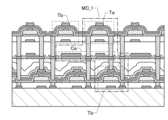
<メモリセルアレイの構成例>
図3(A)は、メモリセルアレイの一例を示す模式図である。図3(A)に示すメモリ
セルアレイ300には、サブアレイSCAが、平面において横a個×縦b個(a、bは自
然数)のアレイ状に配置されている。各サブアレイSCAは、積層されているc個(cは
自然数)のメモリセルMCからなる。このように、メモリセルアレイ300はメモリセル
MCが3次元的に配列されている構造を有する。<Configuration example of memory cell array>
Fig. 3A is a schematic diagram showing an example of a memory cell array. In the
明細書、図面において、同じ要素(信号、配線、素子、回路等)を区別するため、”_
1”、”[L1]”などの行番号、列番号、順序等を表す識別記号を用語に付ける場合が
ある。例えば、”MC_j”とは、サブアレイSCAの第j(jは1からcまでの自然数
)のメモリセルMCであることを表している。 In the specification and drawings, in order to distinguish between the same elements (signals, wiring, elements, circuits, etc.), "
In some cases, an identification symbol such as "[L1]" or "[L1]" may be added to a term to indicate the row number, column number, order, etc. For example, "MC_j" indicates the jth (j is a natural number from 1 to c) memory cell MC in the sub-array SCA.
メモリセルMCは、記憶回路25―27(図2)と同様な回路構成とすることができる
。図3(B)にメモリセルMC_jの回路図の一例を示す。図3(B)に示すメモリセル
MC_jは、トランジスタTa_j、トランジスタTb_j及び容量素子Ca_jを有す
る。図3(B)に示すメモリセルMC_jは、図2(A)に示す記憶回路25の変形例で
ある。ここで、”Ta_j”の符号は、トランジスタTaがメモリセルMC_jの構成要
素であることを示している。他の図面でも、このような符号を用いる場合がある。 The memory cell MC can have a circuit configuration similar to that of the memory circuit 25-27 (FIG. 2). FIG. 3B shows an example of a circuit diagram of a memory cell MC_j. The memory cell MC_j shown in FIG. 3B has a transistor Ta_j, a transistor Tb_j, and a capacitor Ca_j. The memory cell MC_j shown in FIG. 3B is a modified example of the
トランジスタTa_jの第1端子は配線BLと電気的に接続され、第2端子はトランジ
スタTb_jのゲート電極と電気的に接続されている。トランジスタTa_jのゲート電
極は配線WWL_jに電気的に接続されている。トランジスタTb_jの第1端子は配線
BLと電気的に接続され、第2端子は配線SLと電気的に接続されている。容量素子Ca
_jの第1端子(第1電極)はトランジスタTb_jのゲート電極と電気的に接続され、
第2端子(第2電極)は配線RWL_jと電気的に接続される。 A first terminal of the transistor Ta_j is electrically connected to the wiring BL, and a second terminal of the transistor Ta_j is electrically connected to the gate electrode of the transistor Tb_j. The gate electrode of the transistor Ta_j is electrically connected to the wiring WWL_j. A first terminal of the transistor Tb_j is electrically connected to the wiring BL, and a second terminal of the transistor Tb_j is electrically connected to the wiring SL.
a first terminal (first electrode) of the transistor Tb_j is electrically connected to a gate electrode of the transistor Tb_j,
The second terminal (second electrode) is electrically connected to the wiring RWL_j.
トランジスタTa_jは、バックゲート電極(BG)を有する。例えば、バックゲート
電極にソース電極よりも低い電位または高い電位を印加することができるため、トランジ
スタTa_jのしきい値電圧をプラス方向またはマイナス方向へ変動させることができる
。nチャネル型トランジスタのしきい値電圧をプラス方向に変動させることで、ゲート電
位が0Vであってもトランジスタが非導通状態(オフ状態)となる、ノーマリーオフが実
現できる場合がある。なお、バックゲート電極に印加する電位は、可変であってもよいし
、固定であってもよい。バックゲート電極に印加する電位を可変にする場合、電位を制御
する回路をバックゲート電極に接続してもよい。また、バックゲート電極は、トランジス
タTa_jのゲート電極と接続してもよい。バックゲート電極とゲート電極とを接続し、
同じ電位を印加することにより、オン電流の増加、初期特性バラつきの低減、-GBT(
-Gate Bias-Temperature)ストレス試験の劣化の抑制、及び異な
るドレイン電圧におけるオン電流の立ち上がり電圧の変動の抑制が可能である。トランジ
スタTa_jのオン電流を増加させることにより、例えばメモリセルアレイ300の書き
込み時間を短縮することができる。 The transistor Ta_j has a back gate electrode (BG). For example, a lower or higher potential than that of the source electrode can be applied to the back gate electrode, so that the threshold voltage of the transistor Ta_j can be shifted in the positive or negative direction. By shifting the threshold voltage of an n-channel transistor in the positive direction, a normally-off transistor in which the transistor is in a non-conducting state (off state) even when the gate potential is 0 V can be realized. Note that the potential applied to the back gate electrode may be variable or fixed. When the potential applied to the back gate electrode is made variable, a circuit for controlling the potential may be connected to the back gate electrode. The back gate electrode may be connected to the gate electrode of the transistor Ta_j. The back gate electrode and the gate electrode are connected to each other,
By applying the same potential, the on-current increases, the initial characteristic variations are reduced, and the -GBT (
In addition, it is possible to suppress deterioration in a (-Gate Bias-Temperature) stress test and suppress fluctuations in the rise voltage of the on-current at different drain voltages. By increasing the on-current of the transistor Ta_j, it is possible to shorten the write time of the
また、図3(B)には図示しないが、トランジスタTb_jも、バックゲート電極を有
してもよい。バックゲート電極を設けることで、トランジスタTb_jのオン電流を増加
させることが可能であり、オン電流の増加により、例えばメモリセルアレイ300の読み
出し速度を高めることができる。 3B, the transistor Tb_j may also have a backgate electrode. By providing the backgate electrode, the on-state current of the transistor Tb_j can be increased. The increase in the on-state current can increase the read speed of the
ここでは、配線WWL_jに与えられるワード信号を制御することで、ノードFNの電
位が配線BLの電位に応じた電位にすることを、メモリセルMC_jにデータを書き込む
、という。また、配線RWL_jに与えられる読み出し信号を制御することで、配線BL
の電位をノードFNの電位に応じた電位にすることを、メモリセルMC_jからデータを
読み出す、という。 Here, writing data to the memory cell MC_j means changing the potential of the node FN to a potential corresponding to the potential of the wiring BL by controlling a word signal applied to the wiring WWL_j.
Setting the potential of the memory cell MC_j to a potential corresponding to the potential of the node FN is referred to as reading data from the memory cell MC_j.
配線BLには、2値、または多値のデータに対応する電位が与えられる。多値のデータ
は、kビット(kは2以上の自然数)のデータである。具体的には、2ビットのデータで
あれば4値のデータであり、配線BLに入力される信号は4種類の電位レベルを有するこ
とになる。配線RWL_jには、読み出し信号が与えられる。読み出し信号は、メモリセ
ルMC_jからデータを選択的に読み出すために、ノードFNの電位を制御するための信
号である。また、配線WWL_jには、ワード信号が与えられる。ワード信号は、配線B
Lの電位をノードFNに与えるために、トランジスタTa_jを導通状態とする信号であ
る。 A potential corresponding to binary or multi-valued data is applied to the wiring BL. Multi-valued data is k-bit data (k is a natural number equal to or greater than 2). Specifically, 2-bit data is four-valued data, and a signal input to the wiring BL has four types of potential levels. A read signal is applied to the wiring RWL_j. The read signal is a signal for controlling the potential of the node FN in order to selectively read data from the memory cell MC_j. A word signal is applied to the wiring WWL_j. The word signal is input to the wiring B
This is a signal that turns on the transistor Ta_j in order to provide the potential of L to the node FN.
ノードFNは、容量素子Ca_jの第1電極、トランジスタTa_jの第2端子、及び
トランジスタTb_jのゲート電極を接続する配線上のいずれかのノードに相当する。例
えば、ノードFNに液晶素子や有機EL(Electroluminescence)素
子などの表示素子を電気的に接続してもよい。上記表示素子を有する場合、メモリセルM
C_jの一部を表示装置の画素として機能させることができる。 The node FN corresponds to any node on the wiring that connects the first electrode of the capacitor Ca_j, the second terminal of the transistor Ta_j, and the gate electrode of the transistor Tb_j. For example, a display element such as a liquid crystal element or an organic EL (Electroluminescence) element may be electrically connected to the node FN.
A portion of C_j can function as pixels of a display device.
ノードFNの電位は、配線BLに与えられるデータに基づく電位である。ノードFNは
、トランジスタTa_jを非導通状態とすることで電気的に浮遊状態になり、また、容量
素子Ca_jによって配線RWL_jとトランジスタTb_jが容量結合している。その
ため、配線RWL_jの電位を変化させることで、ノードFNの電位を変化させることが
できる。配線RWL_jに与えられる読み出し信号の電位を変化させると、ノードFNの
電位は元の電位に読み出し信号の電位の変化分が加わった電位となる。 The potential of the node FN is a potential based on data supplied to the wiring BL. The node FN is in an electrically floating state by turning off the transistor Ta_j, and the wiring RWL_j and the transistor Tb_j are capacitively coupled by the capacitor Ca_j. Therefore, the potential of the node FN can be changed by changing the potential of the wiring RWL_j. When the potential of the read signal supplied to the wiring RWL_j is changed, the potential of the node FN becomes the sum of the original potential and the change in the potential of the read signal.
トランジスタTa_jは、導通状態と非導通状態とを切り換えることで、データの書き
込みを制御するスイッチとしての機能を有する。また、トランジスタTa_jは、非導通
状態を維持することで、書き込んだデータに基づく電位を保持する機能を有する。ここで
は、トランジスタTa_jはnチャネル型のトランジスタとする。 The transistor Ta_j has a function as a switch that controls writing of data by switching between a conductive state and a non-conductive state. The transistor Ta_j also has a function of holding a potential based on written data by maintaining a non-conductive state. Here, the transistor Ta_j is an n-channel transistor.
なお、トランジスタTa_jは、非導通状態においてソース電極とドレイン電極との間
を流れる電流(オフ電流)が低いトランジスタが用いられることが好適である。ここでは
、オフ電流が低いとは、室温において、ソース電極とドレイン電極との間の電圧を10V
とし、チャネル幅1μmあたりの規格化されたオフ電流が10zA以下であることをいう
。このようにオフ電流が少ないトランジスタとしては、半導体層に酸化物半導体を有する
トランジスタが挙げられる。 Note that the transistor Ta_j is preferably a transistor that has a low current (off-state current) flowing between the source electrode and the drain electrode in a non-conducting state. Here, the term "low off-state current" means that the voltage between the source electrode and the drain electrode is 10 V at room temperature.
This means that the normalized off-state current per 1 μm of channel width is 10 zA or less. An example of a transistor with such a low off-state current is a transistor that includes an oxide semiconductor in a semiconductor layer.
トランジスタTa_jにオフ電流の小さいトランジスタを用いることによって、電気的
に浮遊状態とされているノードFNの電位を長期間に渡って保持することができる。した
がって、メモリセルMC_jのリフレッシュ頻度を低減することができるため、消費電力
の少ない半導体装置を実現することができる。 By using a transistor with low off-state current as the transistor Ta_j, the potential of the node FN which is in an electrically floating state can be held for a long period of time, which reduces the frequency of refreshing the memory cell MC_j, thereby making it possible to realize a semiconductor device with low power consumption.
例えば、ノードFNに保持された電位を85℃において10年間(3.15×10⁸秒
)保持するためには、トランジスタTa_jは、容量1fFあたり、規格化されたオフ電
流値が4.3yA(ヨクトアンペア:1yAは1×10-24A)未満であることが好ま
しい。この場合、ノードFNの許容される電位の変動が0.5V以内であることが好まし
い。または、95℃において、規格化されたオフ電流が1.5yA未満であることが好ま
しい。 For example, in order to hold the potential held at the node FN for 10 years (3.15×10⁸ seconds) at 85° C., the transistor Ta_j preferably has a normalized off-current value of less than 4.3 yA (yoctoampere: 1 yA is 1×10⁻²⁴ A) per capacitance of 1 fF. In this case, the allowable fluctuation in the potential of the node FN is preferably within 0.5 V. Alternatively, the normalized off-current at 95° C. is preferably less than 1.5 yA.
図3(B)に示すメモリセルMC_jの構成では、トランジスタTa_jの非導通状態
を維持することで、ノードFNの電位を保持している。そのため、ノードFNでの電荷の
移動を伴った電位の変動を抑えることが可能なスイッチとして、トランジスタTa_jは
オフ電流が少ないトランジスタであることが特に好ましい。 3B, the transistor Ta_j is kept off to hold the potential of the node FN. Therefore, it is particularly preferable that the transistor Ta_j be a transistor with low off-state current as a switch capable of suppressing a potential fluctuation accompanied by transfer of charge at the node FN.
よって、トランジスタTa_jをオフ電流が少ないトランジスタとすることで、メモリ
セルアレイ300を不揮発性のメモリとすることができる。つまり、一旦、メモリセルM
C_jに書き込まれたデータは、再度、トランジスタTa_jを導通状態とするまで、ノ
ードFNに保持し続けることができる。 Therefore, by using the transistor Ta_j as a transistor with a small off-state current, the
The data written to C_j can be held in the node FN until the transistor Ta_j is turned on again.
トランジスタTb_jは、ノードFNの電位に従って、ソース電極とドレイン電極との
間に電流Idを流す機能を有する。図3(B)に示すメモリセルMC_jの構成では、ト
ランジスタTb_jのソース電極とドレイン電極との間に流れる電流Idは、配線BLと
配線SLとの間に流れる電流である。トランジスタTb_jは、例えばシリコンを活性層
に用いたトランジスタ(以下、Siトランジスタと呼ぶ)を用いてもよく、また酸化物半
導体を活性層に用いたOSトランジスタを用いてもよい。ここでは、トランジスタTb_
jはOSトランジスタであり、かつnチャネル型のトランジスタとする。 The transistor Tb_j has a function of causing a current Id to flow between the source electrode and the drain electrode in accordance with the potential of the node FN. In the configuration of the memory cell MC_j illustrated in FIG. 3B, the current Id flowing between the source electrode and the drain electrode of the transistor Tb_j is a current flowing between the wiring BL and the wiring SL. The transistor Tb_j may be, for example, a transistor using silicon for an active layer (hereinafter referred to as a Si transistor) or an OS transistor using an oxide semiconductor for an active layer. Here, the transistor Tb_j
The transistor j is an OS transistor and is an n-channel transistor.
トランジスタTa_j及びトランジスタTb_jは、一例として、スイッチング速度の
速いnチャネル型トランジスタを用いることができる。例えば、トランジスタのスイッチ
ング速度は、0.1n秒以上5n秒未満である。一例として、チャネル領域が酸化物半導
体(好ましくはIn、Ga、及びZnを含む酸化物)を含むOSトランジスタを用いるこ
とで、上記のスイッチング速度を実現することができる。なお、トランジスタのスイッチ
ング速度とは、一つのトランジスタが非導通状態から導通状態となる時間を表す。或いは
、トランジスタのスイッチング速度とは、トランジスタを増幅器として用いる場合に、電
流利得が1以上となる最大の周波数(遮断周波数)に対応する速度で表しても良い。 For example, n-channel transistors with a high switching speed can be used as the transistors Ta_j and Tb_j. For example, the switching speed of the transistors is 0.1 nsec or more and less than 5 nsec. For example, the above switching speed can be achieved by using an OS transistor whose channel region contains an oxide semiconductor (preferably an oxide containing In, Ga, and Zn). Note that the switching speed of a transistor refers to the time it takes for a transistor to change from a non-conducting state to a conducting state. Alternatively, the switching speed of a transistor may be expressed as a speed corresponding to a maximum frequency (cutoff frequency) at which a current gain is 1 or more when the transistor is used as an amplifier.
<メモリセルアレイの回路構成例1>
ここで、図3(B)に示すメモリセルMC_jを3次元的に配列し、メモリセルアレイ
300とする場合の一例を図4に示す。図4は、メモリセルアレイ300の一例を示す回
路図であり、サブアレイSCAの一例を示す回路図でもある。図4に示すように、サブア
レイSCAはc個のメモリセルMCを有し、各メモリセルMCは、それぞれ、配線BL及
び配線SLを共有している。<Circuit configuration example 1 of memory cell array>
Here, an example of a
<メモリセルアレイの動作例>
次に、図4に示すメモリセルアレイ300の動作を説明する。図5は、図4に示すメモ
リセルアレイ300の動作の一例を説明するタイミングチャートである。図5のタイミン
グチャートは、配線WWL_c、配線RWL_c、ノードFN、配線BL、及び配線SL
に与えられる各信号の変化を示すものである。<Example of memory cell array operation>
Next, an operation of the
, which shows the changes in each signal applied to
まず、図5(A)を用いて、書き込みの動作を説明する。ここでは2値のデータの書き
込みについて説明を行うが、メモリセルアレイ300は2値のデータの書き込みに限定さ
れず、多値のデータを書き込むこともできる。図5(A)に示すタイミングチャートには
、書き込み期間T1、休止期間T2、及び非選択期間T3を示す。 First, the write operation will be described with reference to Fig. 5A. Here, the write of binary data will be described, but the
書き込み期間T1では、まず配線WWL_cに電位V2が与えられる。次いで、配線B
Lに2値のデータに応じた電位、つまりハイ(H)レベルの電位またはロー(L)レベル
の電位が与えられる。また、配線SLには、配線BLと同じレベルの電位を与える。配線
BLがHレベルの時、配線SLにもHレベルの電位が与えられる。配線BLがLレベルの
時、配線SLにも、Lレベルの電位が与えられる。 In the writing period T1, first, a potential V2 is applied to the wiring WWL_c.
A potential corresponding to binary data, that is, a high (H) level potential or a low (L) level potential, is applied to the wiring L. A potential of the same level as that of the wiring BL is applied to the wiring SL. When the wiring BL is at the H level, an H level potential is also applied to the wiring SL. When the wiring BL is at the L level, an L level potential is also applied to the wiring SL.
休止期間T2では、配線BL及び配線SLにLレベルの電位が与えられ、配線RWL_
c及び配線WWL_cには電位V0が与えられる。ここで、例えば電位V0は接地電位と
し、電位V2は正の電位とすればよい。また、電位V2の絶対値は、Hレベルの電位より
大きいことが好ましく、例えば、Hレベルの電位+トランジスタTa_cのしきい値電圧
よりも大きく、且つHレベルの電位+トランジスタTa_cのしきい値電圧の3倍未満と
すればよい。 In the idle period T2, an L-level potential is applied to the wiring BL and the wiring SL.
A potential V0 is applied to the wiring WWL_c and the wiring WWL_c. Here, for example, the potential V0 may be a ground potential, and the potential V2 may be a positive potential. The absolute value of the potential V2 is preferably larger than the H-level potential, and may be, for example, larger than the H-level potential plus the threshold voltage of the transistor Ta_c and less than three times the H-level potential plus the threshold voltage of the transistor Ta_c.
非選択期間T3では、配線RWL_c及び配線WWL_cに電位V1が与えられる。電
位V1は例えば負の電位とすればよい。電位V1の絶対値は、Hレベルの電位より大きい
ことが好ましく、例えば、Hレベルの電位+トランジスタTb_cのしきい値電圧よりも
大きく、且つHレベルの電位+トランジスタTb_cのしきい値電圧の3倍未満とすれば
よい。また、配線BL及び配線SLにはLレベルの電位が与えられる。 In the non-selection period T3, a potential V1 is applied to the wiring RWL_c and the wiring WWL_c. The potential V1 may be, for example, a negative potential. The absolute value of the potential V1 is preferably larger than an H-level potential, and may be, for example, larger than the H-level potential plus the threshold voltage of the transistor Tb_c and less than the H-level potential plus three times the threshold voltage of the transistor Tb_c. In addition, an L-level potential is applied to the wiring BL and the wiring SL.
次に、図5(B)を用いて、読み出しの動作について説明する。図5(B)に示すタイ
ミングチャートには、配線BLの電位をプリチャージする期間T4、データを読み出すた
めに配線BLの放電を行う期間T5、非選択の期間T6を示している。 Next, the read operation will be described with reference to Fig. 5B. The timing chart shown in Fig. 5B shows a period T4 in which the potential of the wiring BL is precharged, a period T5 in which the wiring BL is discharged in order to read data, and a non-selection period T6.
図5(B)に示す期間T4では、配線BLをプリチャージする。このとき、配線WWL
_cに電位V1が与えられる。また、配線RWL_cは、電位V1が与えられる。ここで
、V1は、V0よりも低い電位である。例えば、V0を接地電位とし、V1を負の電位と
すればよい。また、ノードFNでは、データに対応する電位が保持されている。また、配
線BLは、Hレベルの電位(VH)が与えられる。また、配線SLは、Lレベルの電位が
与えられる。ここで、電位V1の絶対値は、Hレベルの電位より大きいことが好ましく、
例えば、Hレベルの電位+トランジスタTb_cのしきい値電圧よりも大きく、且つHレ
ベルの電位+トランジスタTb_cのしきい値電圧の3倍未満にすればよい。 In the period T4 shown in FIG. 5B, the wiring BL is precharged.
A potential V1 is applied to the wiring RWL_c. A potential V1 is applied to the wiring RWL_c. Here, V1 is a potential lower than V0. For example, V0 may be a ground potential, and V1 may be a negative potential. A potential corresponding to data is held in the node FN. An H-level potential (VH) is applied to the wiring BL. An L-level potential is applied to the wiring SL. Here, the absolute value of the potential V1 is preferably larger than the H-level potential,
For example, it may be set to a value greater than the H-level potential plus the threshold voltage of the transistor Tb_c and less than three times the H-level potential plus the threshold voltage of the transistor Tb_c.
期間T4では、配線BLは、Hレベルの電位VHが与えられた後、電気的に浮遊状態と
なる。すなわち、配線BLは、電荷の充電又は放電により電位の変動が生じる状態となる
。この浮遊状態は、配線BLに電位を与えるスイッチをオフにすることで実現できる。 In the period T4, the wiring BL is supplied with an H-level potential VH and then is placed in an electrically floating state. That is, the wiring BL is placed in a state in which a potential fluctuates due to charging or discharging of electric charge. This floating state can be achieved by turning off a switch that supplies a potential to the wiring BL.
次いで、図5(B)に示す期間T5では、データを読み出すためにノードFNの電位に
より配線BLの放電を行う。このとき、配線WWL_cは、期間T4に引き続き、電位V
1が与えられる。配線SLは、前の期間に引き続き、Lレベルの電位が与えられる。配線
RWL_cは、電位V0の電位が与えられるため、ノードFNの電位が上昇する。ノード
FNの電位により、トランジスタTb_cの導通状態が変化する。ノードFNにHレベル
の電位が書き込まれている場合には、トランジスタTb_cが導通状態となり、配線BL
の電位は降下し、電位VLとなる。ノードFNにLレベルの電位が書き込まれている場合
には、トランジスタTb_cが非導通状態のため、配線BLの電位はHレベルの状態が維
持される。 Next, in the period T5 shown in FIG. 5B, the wiring BL is discharged by the potential of the node FN in order to read data. At this time, the wiring WWL_c is discharged at the potential V
1 is applied to the wiring SL as in the previous period. Since the potential V0 is applied to the wiring RWL_c, the potential of the node FN rises. The conduction state of the transistor Tb_c changes depending on the potential of the node FN. When an H-level potential is written to the node FN, the transistor Tb_c is turned on, and the wiring BL
The potential of the wiring BL drops to the potential VL. When an L-level potential is written to the node FN, the transistor Tb_c is off, so that the potential of the wiring BL is kept at the H-level.
次いで、図5(B)に示す期間T6では、配線RWL_cの電位をV1とし、メモリセ
ルMC_cを非選択の状態にする。これで、メモリセルMC_cからデータを読み出す動
作が完了する。 5B, the potential of the wiring RWL_c is set to V1, and the memory cell MC_c is put into an unselected state, completing the operation of reading data from the memory cell MC_c.
<メモリセルアレイの回路構成例2、3>
メモリセルアレイ300の他の回路構成例を図6及び図7に示す。図6及び図7は、メ
モリセルアレイ300の一例を示す回路図であり、サブアレイSCAの回路図である。<Circuit configuration examples 2 and 3 of memory cell array>
6 and 7 show other examples of the circuit configuration of the
図6の回路構成例は、図4の変形例である。図4の例と異なる点は、奇数番のメモリセ
ルMCと偶数番のメモリセルMCとが異なる配線SLに電気的に接続されていること、配
線BLに対して、奇数番のメモリセルMCと偶数番のメモリセルMCが互い違いに接続さ
れていることである。そのため、サブアレイSCAの集積度を高めることができる。また
は、面積あたりの記憶容量を高めることができる。図7に示すサブアレイSCAでは、c
個のメモリセルMCが1つの配線SLを共有している。このため、配線SLの本数を少な
くすることができる。 The circuit configuration example of Fig. 6 is a modified example of Fig. 4. The difference from the example of Fig. 4 is that the odd-numbered memory cells MC and the even-numbered memory cells MC are electrically connected to different wirings SL, and that the odd-numbered memory cells MC and the even-numbered memory cells MC are alternately connected to the wirings BL. This makes it possible to increase the integration degree of the sub-array SCA. Alternatively, it makes it possible to increase the memory capacity per area. In the sub-array SCA shown in Fig. 7,
The memory cells MC share one wiring SL, so that the number of wirings SL can be reduced.
<メモリセルの積層構造例1>
図8はメモリセルアレイの一例を示す断面図である。図8の例は、図4の回路構成を有
するサブアレイSCAでメモリセルアレイを構成した例に相当する。<Memory Cell Stack Structure Example 1>
8 is a cross-sectional view showing an example of a memory cell array, which corresponds to an example in which the memory cell array is configured with sub-arrays SCA each having the circuit configuration shown in FIG.
図8には、隣接する3つのサブアレイ(SCA[α-1]、SCA[α]、SCA[α
+1])を図示している。サブアレイSCAが互いに隣接するとは、図3(A)に示すx
y平面においてx座標、y座標の一方が1異なり、他方が同じであることを示す。例えば
、3つのサブアレイ(SCA[α-1]、SCA[α]、SCA[α+1])のy座標が
等しい場合、サブアレイSCA[α]のx座標がk(kは2以上a以下の整数)であれば
、サブアレイSCA[α-1]のx座標はk-1であり、サブアレイSCA[α+1]の
x座標はk+1である。 FIG. 8 shows three adjacent subarrays (SCA[α-1], SCA[α], and SCA[α
The sub-arrays SCA being adjacent to each other are the x
This indicates that one of the x and y coordinates differs by 1 in the y plane, and the other is the same. For example, when the y coordinates of three subarrays (SCA[α-1], SCA[α], SCA[α+1]) are equal, if the x coordinate of the subarray SCA[α] is k (k is an integer between 2 and a), the x coordinate of the subarray SCA[α-1] is k-1, and the x coordinate of the subarray SCA[α+1] is k+1.
図8には、サブアレイ(SCA[α-1]、SCA[α]、SCA[α+1])のメモ
リセルMC_1及びメモリセルMC_2を示している。図示しないが、各サブアレイのメ
モリセルMC_2の上には,それぞれ、メモリセルMC_3が積層され、順にメモリセル
MC_cまで積層される。メモリセルMCの積層数を多くすることで、回路面積を増加さ
せずに、メモリセルアレイ300の集積度を高めることができる。 8 shows memory cells MC_1 and MC_2 of subarrays (SCA[α-1], SCA[α], SCA[α+1]). Although not shown, memory cells MC_3 are stacked on top of memory cells MC_2 of each subarray, and are stacked in order up to memory cell MC_c. By increasing the number of stacked memory cells MC, it is possible to increase the integration density of the
以下、図8に示すメモリセルアレイ300のデバイス構造について説明する。図8にお
いて、図面の明瞭化のため、メモリセルアレイ300を構成する一部の要素(トランジス
タTa等)の符号には、識別記号”_1”を付けていない。明細書中では、識別符号”_
1”等を付して、または付けずに、メモリセルアレイ300の構造を説明する場合がある
。他の図面についても同様である。 The device structure of the
The structure of the
各メモリセルMCは、トランジスタTa及びトランジスタTbは、酸化物半導体材料を
含んで構成される。トランジスタTbの上には容量素子Caが設けられている。トランジ
スタTbと容量素子Caの間には絶縁膜216が設けられている。容量素子Caの少なく
とも一部は、トランジスタTbと重なるように設けられることが好ましい。絶縁膜115
は、導電膜151及び導電膜155に挟まれ、容量素子Caを形成する。導電膜204a
、導電膜204bは、それぞれ、トランジスタTbのソース電極またはドレイン電極とし
て機能する。導電膜151は、プラグ141を介してトランジスタTbのゲート電極20
3と電気的に接続される。 In each memory cell MC, the transistor Ta and the transistor Tb are formed of an oxide semiconductor material. A capacitor Ca is provided over the transistor Tb. An insulating
The
The
3 is electrically connected to
容量素子Caの上にはトランジスタTaが設けられている。容量素子Caとトランジス
タTaの間には絶縁膜156が設けられている。トランジスタTaの少なくとも一部は、
容量素子Caと重なるように設けられることが好ましい。導電膜104a、導電膜104
bはそれぞれ、トランジスタTaのソース電極またはドレイン電極として機能する。 The transistor Ta is provided on the capacitance element Ca. An insulating
It is preferable that the
b function as the source electrode and the drain electrode of the transistor Ta, respectively.
導電膜204a、204bは配線SL(図示しない)に電気的に接続される。導電膜2
04aは、プラグ142、導電膜153、及びプラグ145等を介して導電膜104aと
電気的に接続される。導電膜204a及び導電膜104aは配線BL(図示しない)に電
気的に接続されている。プラグ142、導電膜153、及びプラグ145等を配線BLと
して機能させてもよい。 The
The
隣接する2つのメモリセルMC_jは、プラグ142、導電膜153等を共有する。具
体的には、サブアレイSCA[α]のメモリセルMC_jは、サブアレイSCA[α-1
]のメモリセルMC_jと、プラグ142、プラグ145および導電膜153を共有する
。隣接する2つのサブアレイSCAでプラグや導電層を共有することにより、メモリセル
アレイ300の集積度を高めることができる。 Two adjacent memory cells MC_j share the
], the
また、隣接するMC_jにおいて導電膜104aおよび導電膜204bが共有されてい
る。具体的には、サブアレイSCA[α-1]とサブアレイSCA[α]のそれぞれのト
ランジスタTaは、導電膜104aを共有する。サブアレイSCA[α]とサブアレイS
CA[α+1]のそれぞれのトランジスタTbは導電膜204aを共有する。このように
導電膜を共有することにより、メモリセルアレイ300の集積度を高めることができる。 In addition, the
The transistors Tb of CA[α+1] share the
<メモリセルの積層構造例2>
図9及び図10に、図8示すメモリセルアレイ300の変形例を示す。図10は図9の
一部を拡大した図である。図9に示すメモリセルアレイ300は基板100上に形成され
、層291乃至層297を有する。また、層291はトランジスタを有する。また、層2
92及び層293は導電膜を有する。また、層294はトランジスタを有する。また、層
295及び層296は導電膜を有する。また、層297はトランジスタを有する。<Memory Cell Stack Structure Example 2>
9 and 10 show modified examples of the
The
図8に示すメモリセルアレイ300のサブアレイSCAでは、トランジスタTb、容量
素子Ca、トランジスタTa、トランジスタTb、容量素子Ca、トランジスタTaの順
に積層されている。これに対し、図9に示すサブアレイSCAでは、メモリセルMCを互
い違いに配置することによりトランジスタTb、容量素子Ca、トランジスタTa、容量
素子Ca、トランジスタTbの順に積層される。よって、工程を簡略化することができる
。 In the subarray SCA of the
メモリセルMCにおいて、トランジスタTbの上には容量素子Caが設けられ、容量素
子Ca上にトランジスタTaが設けられている。容量素子Caは、トランジスタTbと重
なる領域を有し、また、トランジスタTaと重なる領域を有することが好ましい。また、
容量素子Caの一部は、隣接するメモリセルMCのトランジスタTbと重なる領域を有し
ていてもよい。図9に示すようなデバイス構造とすることで、メモリセルアレイ300の
集積度を高めることができる。 In the memory cell MC, a capacitance element Ca is provided on the transistor Tb, and a transistor Ta is provided on the capacitance element Ca. The capacitance element Ca has an area overlapping with the transistor Tb, and preferably has an area overlapping with the transistor Ta.
A part of the capacitance element Ca may have an area overlapping with the transistor Tb of the adjacent memory cell MC. By using the device structure as shown in FIG.
具体的には、サブアレイSCA[α]において、メモリセルMC_2とメモリセルMC
_3は左右対称の構造を有する。そのため、容量素子Caは、トランジスタTa、および
トランジスタTbと重なっている。このような構造とすることにより、サブアレイSCA
において、メモリセルMCを互い違いに配置することができ、1つ下のメモリセルMCの
トランジスタTa上に容量素子を形成することができ、集積度を高めることができる。図
8に示すメモリセルアレイ300と比べて工程を簡略化することができる。 Specifically, in the subarray SCA[α], the memory cell MC_2 and the memory cell MC
The subarray SCA_3 has a symmetrical structure. Therefore, the capacitance element Ca overlaps with the transistor Ta and the transistor Tb.
In the
また、サブアレイSCA[α]において、c個のメモリセルMCを互い違いに配置する
ことにより、上下に隣接する2つのメモリセルMCでは、それぞれ、トランジスタTaと
トランジスタTbとが同じ層に形成される。このように、上下に隣接するメモリセルの有
するトランジスタが同一層に形成されることで、メモリセルアレイ300を構成する層の
数が削減されるため、より少ない工程でメモリセルアレイ300を作製することができる
。少ない工程で作製することにより、歩留まりを高めることができる。また、積層される
層数が増えるのに伴い、例えば、絶縁膜、導電膜、半導体膜等が有する膜応力により、膜
の剥がれや割れなどが生じる可能性がある。よって、積層される膜の数を少なくすること
により、膜剥がれ等による半導体装置の故障を低減することができる。 In addition, by arranging the c memory cells MC alternately in the subarray SCA[α], the transistors Ta and Tb are formed in the same layer in two memory cells MC adjacent to each other vertically. In this way, the transistors of the memory cells adjacent to each other vertically are formed in the same layer, so that the number of layers constituting the
<メモリセルの積層構造例3>
図11にメモリセルアレイの一例を示す。図11に示すメモリセルアレイ300は、図
8及び図9に示すメモリセルアレイ300の変形例である。<Memory Cell Stack Structure Example 3>
An example of a memory cell array is shown in Fig. 11. The
図11に示すメモリセルアレイ300は、メモリセルMCが互い違いに配置されている
点で図9と共通する。次の点で相違する。メモリセルMCでは、トランジスタTaの上に
容量素子Caが位置し、容量素子Caの上にトランジスタTbが位置している。また、奇
数番目のメモリセルMC(図11中では、MC_1、MC_3)では、トランジスタTb
のゲート電極203が容量素子Caと電気的に接続されている。偶数番目のメモリセルM
C(図11中ではメモリセルMC_2及びメモリセルMC_4)では、導電膜205が、
容量素子Caと電気的に接続されている。導電膜205は、トランジスタTbのバックゲ
ート電極として機能する。 The
The
In C (memory cell MC_2 and memory cell MC_4 in FIG. 11), the
The
つまり、図11の例では、jが奇数のメモリセルMC_jと,偶数のメモリセルMC_
jとで構造が異なる。また、図11の例では、トランジスタTaとトランジスタTbを同
一の層に形成する必要がなく、トランジスタTaの有する半導体膜とトランジスタTbの
有する半導体膜が異なる半導体膜から形成することができる。そのため、トランジスタT
aとトランジスタTbのそれぞれの半導体膜を、例えば構成元素や原子数比の異なる酸化
物半導体膜で形成することが容易である。 That is, in the example of FIG. 11, there are memory cells MC_j, where j is an odd number, and memory cells MC_
In the example of FIG. 11, the transistors Ta and Tb do not need to be formed in the same layer, and the semiconductor film of the transistor Ta and the semiconductor film of the transistor Tb can be formed from different semiconductor films.
In this case, it is easy to form the semiconductor films of the transistors T1 and Tb using oxide semiconductor films having different constituent elements or atomic ratios.
以上がメモリセルアレイ300の構成例についての説明である。次に、メモリセルアレ
イ300が有するトランジスタTa及びトランジスタTbの構造について説明する。 This concludes the description of the configuration example of the
<トランジスタの構成例1>
図12(B)は、トランジスタの構成の一例を示す上面図であり、図12(A)は、図
12(B)のA-B線断面図であり、図12(C)は図12(B)のC-D線断面図であ
る。図12に示すトランジスタTR1はOSトランジスタであり、メモリセルMCのトラ
ンジスタTaに相当するトランジスタの例である。トランジスタTR1は、トランジスタ
Tbにも適用が可能である。<Transistor Configuration Example 1>
12B is a top view showing an example of the configuration of a transistor, FIG 12A is a cross-sectional view taken along line A-B in FIG 12B, and FIG 12C is a cross-sectional view taken along line C-D in FIG 12B. The transistor TR1 shown in FIG 12 is an OS transistor and is an example of a transistor corresponding to the transistor Ta in the memory cell MC. The transistor TR1 can also be applied to the transistor Tb.
トランジスタTR1は、半導体膜101、導電膜104a、導電膜104b、ゲート絶
縁膜102、ゲート電極103、導電膜105、および絶縁膜114を有する。 The
半導体膜101は、絶縁膜114の上面に接する半導体膜101a、半導体膜101a
の上面に接する半導体膜101b、および半導体膜101bの上面に接する半導体膜10
1cを有する。図12(A)の例では、半導体膜101は、半導体膜101a、半導体膜
101bおよび半導体膜101cの積層構造である。ただし、半導体膜101は、上記積
層構造に限定されず、単層で形成してもよい。ゲート電極103、ゲート絶縁膜102お
よび半導体膜101cの端部が概略一致する。これは、ゲート絶縁膜102および半導体
膜101cを形成するためのエッチング工程で、ゲート電極103がマスクとして機能す
るからである。 The
A
12A, the
導電膜104a及び導電膜104bは、それぞれ、ソース電極またはドレイン電極とし
て機能する。導電膜104a及び導電膜104bは、半導体膜101bの上面と接し、且
つ、その上面で離間されている。半導体膜101cは、半導体膜101b、導電膜104
a及び導電膜104bのそれぞれの上面と接する。ゲート電極103はゲート絶縁膜10
2を介して半導体膜101と対向し、導電膜105は絶縁膜114を介して半導体膜10
1と対向する。導電膜105はトランジスタTR1のバックゲート電極として機能する。 The
The
The
The
別言すると、半導体膜101aは、絶縁膜114と半導体膜101bの間に設けられて
いる。また、半導体膜101cは、半導体膜101bとゲート絶縁膜102の間に設けら
れている。また、導電膜104aおよび導電膜104bは、半導体膜101bの上面に接
し、半導体膜101cの下面と接する。半導体膜101bの側面は、導電膜104aおよ
び導電膜104bと接する。 In other words, the
なお、導電膜105を設けない構成としてもよい。または、図示しないが、導電膜10
5は、ゲート電極103と電気的に接続する構成としてもよい。例えば、導電膜105を
ゲート電極103と電気的に接続し、同じ電位を印加する構成とした場合、オン電流の増
加、初期特性バラつきの低減、-GBT(-Gate Bias-Temperatur
e)ストレス試験の劣化の抑制、及び異なるドレイン電圧におけるオン電流の立ち上がり
電圧の変動の抑制が可能である。トランジスタTR1のオン電流を増加させることにより
、例えばメモリセルアレイ300の読み出し速度を高めることができる。 Note that the
For example, when the
e) It is possible to suppress degradation during stress testing and suppress fluctuations in the on-state current rise voltage at different drain voltages. By increasing the on-state current of the transistor TR1, for example, the read speed of the
また、ゲート電極103の電界によって、半導体膜101bを電気的に取り囲むことが
できる(導電膜の電界によって、半導体膜を電気的に取り囲むトランジスタの構造を、s
urrounded channel(s-channel)構造とよぶ。)。トランジ
スタTR1はs-channel構造のデバイスである。そのため、半導体膜101bの
全体(バルク)にチャネルが形成される場合がある。s-channel構造では、トラ
ンジスタのソース電極-ドレイン電極間に大電流を流すことができ、導通時の電流(オン
電流)を高くすることができる。 In addition, the
This is called a rounded channel (s-channel) structure. The transistor TR1 is an s-channel structure device. Therefore, a channel may be formed in the
上述のs-channel構造は、高いオン電流が得られるため、微細化されたOSト
ランジスタに適した構造といえる。また、OSトランジスタを微細化できるため、該OS
トランジスタを有する半導体装置は、集積度の高い、高密度化された半導体装置とするこ
とが可能となる。例えば、OSトランジスタは、チャネル長が1nm以上100nm未満
、さらに好ましくはチャネル長が5nm以上60nm以下の領域を有すると好ましい。 The above-described s-channel structure can provide a high on-state current and is therefore suitable for miniaturized OS transistors.
A semiconductor device including the transistor can be a semiconductor device with high integration and high density. For example, an OS transistor preferably has a channel length of 1 nm to less than 100 nm, more preferably 5 nm to 60 nm.
なお、チャネル長とは、例えば、トランジスタの上面図において、半導体(またはトラ
ンジスタがオン状態のときに半導体の中で電流の流れる部分)とゲート電極とが重なる領
域、またはチャネルが形成される領域における、ソース(ソース領域またはソース電極)
とドレイン(ドレイン領域またはドレイン電極)との間の距離をいう。なお、一つのトラ
ンジスタにおいて、チャネル長が全ての領域で同じ値をとるとは限らない。即ち、一つの
トランジスタのチャネル長は、一つの値に定まらない場合がある。そのため、本明細書等
では、チャネル長は、チャネルの形成される領域における、いずれか一の値、最大値、最
小値または平均値とする。 Note that the channel length is, for example, the length of a region where a semiconductor (or a portion where a current flows in the semiconductor when the transistor is on) overlaps with a gate electrode in a top view of a transistor, or the length of a source (source region or source electrode) in a region where a channel is formed.
The channel length refers to the distance between the drain (drain region or drain electrode) and the source. Note that the channel length of one transistor does not necessarily have the same value in all regions. That is, the channel length of one transistor may not be determined to one value. Therefore, in this specification and the like, the channel length refers to any one value, maximum value, minimum value, or average value in the region where the channel is formed.
また、チャネル幅とは、例えば、半導体(またはトランジスタがオン状態のときに半導
体の中で電流の流れる部分)とゲート電極とが重なる領域、またはチャネルが形成される
領域における、ソース(ソース領域またはソース電極)とドレイン(ドレイン領域または
ドレイン電極)とが向かい合っている部分の長さをいう。なお、一つのトランジスタにお
いて、チャネル幅がすべての領域で同じ値をとるとは限らない。即ち、一つのトランジス
タのチャネル幅は、一つの値に定まらない場合がある。そのため、本明細書では、チャネ
ル幅は、チャネルの形成される領域における、いずれか一の値、最大値、最小値または平
均値とする。 The channel width refers to, for example, the length of the portion where the source (source region or source electrode) and the drain (drain region or drain electrode) face each other in the region where the semiconductor (or the portion in the semiconductor through which current flows when the transistor is on) and the gate electrode overlap, or in the region where the channel is formed. Note that the channel width of one transistor does not necessarily have the same value in all regions. That is, the channel width of one transistor may not be determined to one value. Therefore, in this specification, the channel width is defined as any one value, maximum value, minimum value, or average value in the region where the channel is formed.
なお、トランジスタの構造によっては、実際にチャネルの形成される領域におけるチャ
ネル幅(以下、実効的なチャネル幅と呼ぶ。)と、トランジスタの上面図において示され
るチャネル幅(以下、見かけ上のチャネル幅と呼ぶ。)と、が異なる場合がある。例えば
、立体的な構造を有するトランジスタでは、実効的なチャネル幅が、トランジスタの上面
図において示される見かけ上のチャネル幅よりも大きくなり、その影響が無視できなくな
る場合がある。例えば、微細かつ立体的な構造を有するトランジスタでは、半導体の上面
に形成されるチャネル領域の割合に対して、半導体の側面に形成されるチャネル領域の割
合が大きくなる場合がある。その場合は、上面図において示される見かけ上のチャネル幅
よりも、実際にチャネルの形成される実効的なチャネル幅の方が大きくなる。 Depending on the structure of the transistor, the channel width in the region where the channel is actually formed (hereinafter referred to as the effective channel width) may differ from the channel width shown in the top view of the transistor (hereinafter referred to as the apparent channel width). For example, in a transistor having a three-dimensional structure, the effective channel width may be larger than the apparent channel width shown in the top view of the transistor, and the influence of this may not be negligible. For example, in a transistor having a fine and three-dimensional structure, the ratio of the channel region formed on the side of the semiconductor may be larger than the ratio of the channel region formed on the top surface of the semiconductor. In that case, the effective channel width where the channel is actually formed is larger than the apparent channel width shown in the top view.
また、立体的な構造を有するトランジスタにおいては、実効的なチャネル幅の、実測に
よる見積もりが困難となる場合がある。例えば、設計値から実効的なチャネル幅を見積も
るためには、半導体の形状が既知という仮定が必要である。したがって、半導体の形状が
正確にわからない場合には、実効的なチャネル幅を正確に測定することは困難である。 In addition, in a transistor having a three-dimensional structure, it may be difficult to estimate the effective channel width by actual measurement. For example, in order to estimate the effective channel width from a design value, it is necessary to assume that the shape of the semiconductor is known. Therefore, if the shape of the semiconductor is not precisely known, it is difficult to accurately measure the effective channel width.
そこで、本明細書等では、トランジスタの上面図において、半導体とゲート電極とが重
なる領域における、ソース(ソース領域またはソース電極)とドレイン(ドレイン領域ま
たはドレイン電極)とが向かい合っている部分の長さである見かけ上のチャネル幅を、「
囲い込みチャネル幅(SCW:Surrounded Channel Width)」
と呼ぶ場合がある。また、本明細書等では、単にチャネル幅と記載した場合には、囲い込
みチャネル幅または見かけ上のチャネル幅を指す場合がある。または、本明細書等では、
単にチャネル幅と記載した場合には、実効的なチャネル幅を指す場合がある。なお、チャ
ネル長、チャネル幅、実効的なチャネル幅、見かけ上のチャネル幅、囲い込みチャネル幅
などは、断面TEM像などを取得して、その画像を解析することなどによって、値を決定
することができる。 Therefore, in this specification and the like, the apparent channel width, which is the length of the portion where the source (source region or source electrode) and the drain (drain region or drain electrode) face each other in the region where the semiconductor and the gate electrode overlap in a top view of a transistor, is defined as "
Surrounded Channel Width (SCW)
In addition, in this specification, when the term "channel width" is used simply, it may refer to the enclosed channel width or the apparent channel width.
When simply described as a channel width, it may refer to an effective channel width. Note that the values of the channel length, channel width, effective channel width, apparent channel width, enclosed channel width, etc. can be determined by acquiring a cross-sectional TEM image or the like and analyzing the image.
なお、トランジスタの電界効果移動度や、チャネル幅当たりの電流値などを計算して求
める場合、囲い込みチャネル幅を用いて計算する場合がある。その場合には、実効的なチ
ャネル幅を用いて計算する場合とは異なる値をとる場合がある。 In addition, when calculating the field effect mobility of a transistor, the current value per channel width, and the like, the calculation may be performed using the enclosed channel width. In that case, the calculated value may be different from the value calculated using the effective channel width.
以下、図12に示すトランジスタTR1が有する各構成要素の詳細について説明する。Below, we will explain in detail each component of transistor TR1 shown in Figure 12.
<下地膜として機能する絶縁膜>
絶縁膜114は、酸化物を含むことが好ましい。特に加熱により酸素を脱離する酸化物
材料を含むことが好ましい。また、半導体膜101は、絶縁膜114上に設けられること
が好ましい。<Insulating film functioning as a base film>
The insulating
加熱により酸素を脱離する酸化物材料として、化学量論的組成を満たす酸素よりも多く
の酸素を含む酸化物を用いることが好ましい。化学量論的組成を満たす酸素よりも多くの
酸素を含む酸化物膜は、昇温脱離ガス分光法(TDS:Thermal Desorpt
ion Spectroscopy)分析にて、酸素原子に換算しての酸素の脱離量が1
.0×1018atoms/cm3以上、好ましくは3.0×1020atoms/cm
3以上である酸化物膜である。なお、上記TDS分析時における膜の表面温度としては1
00℃以上700℃以下、または100℃以上500℃以下の範囲が好ましい。 As the oxide material that releases oxygen by heating, it is preferable to use an oxide that contains more oxygen than the oxygen that satisfies the stoichiometric composition. The oxide film that contains more oxygen than the oxygen that satisfies the stoichiometric composition can be measured by thermal desorption spectroscopy (TDS).
The amount of oxygen released, calculated as oxygen atoms, was 1
0×1018 atoms/cm3 or more, preferably 3.0×10²⁰ atoms/cm
The oxide film has a surface temperature of 1.3 ormore during the TDS analysis.
The range of 00°C or higher and 700°C or lower, or 100°C or higher and 500°C or lower, is preferred.
加熱により酸素を脱離する酸化物材料として、例えば、酸化シリコンまたは酸化窒化シ
リコンを含む材料を用いることが好ましい。または、金属酸化物を用いることもできる。
金属酸化物として、酸化アルミニウム、酸化窒化アルミニウム、酸化ガリウム、酸化窒化
ガリウム、酸化イットリウム、酸化窒化イットリウム、酸化ハフニウム、酸化窒化ハフニ
ウム等を用いる事ができる。なお、本明細書中において、酸化窒化シリコンとは、その組
成として窒素よりも酸素の含有量が多い材料を指し、窒化酸化シリコンとは、その組成と
して、酸素よりも窒素の含有量が多い材料を示す。 As the oxide material that releases oxygen by heating, for example, a material containing silicon oxide or silicon oxynitride is preferably used. Alternatively, a metal oxide can also be used.
Examples of the metal oxide that can be used include aluminum oxide, aluminum oxynitride, gallium oxide, gallium oxynitride, yttrium oxide, yttrium oxynitride, hafnium oxide, hafnium oxynitride, etc. In this specification, silicon oxynitride refers to a material having a higher oxygen content than nitrogen, and silicon nitride oxide refers to a material having a higher nitrogen content than oxygen.
半導体膜101として酸化物半導体を用いた場合、絶縁膜114から脱離した酸素が酸
化物半導体に供給され、酸化物半導体中の酸素欠損を低減することが可能となる。その結
果、トランジスタTR1の電気特性の変動を抑制し、信頼性を高めることができる。 In the case where an oxide semiconductor is used for the
また、絶縁膜114の上面は平坦化処理、例えば、CMP(Chemical Mec
hanical Polishing)法等を用いた平坦化処理により平坦化されている
ことが好ましい。 The upper surface of the insulating
It is preferable that the surface is planarized by a planarization treatment using a method such as a planarization process using a polishing technique.
<半導体膜>
半導体膜101は、シリコンよりもバンドギャップの大きな半導体を含むことが好まし
い。好適には、半導体膜101は酸化物半導体を含んで構成される。シリコンよりもバン
ドギャップが広く、且つキャリア密度の小さい半導体材料を用いると、トランジスタのオ
フ状態における電流を低減できるため好ましい。半導体膜101としてこのような材料を
用いることで、電気特性の変動が抑制され、信頼性の高いトランジスタを実現できる。<Semiconductor film>
The
より具体的には、半導体膜101としては、酸化物半導体膜を用いると好ましい。例え
ば、半導体膜101bとして、In:Ga:Zn=1:1:1、2:1:3、3:1:2
、または4:2:3の原子数比のIn-Ga-Zn酸化物を用いた場合、半導体膜101
aまたは半導体膜101cとして、In:Ga:Zn=1:3:2、1:3:4、1:3
:6、1:6:4、1:6:8、1:6:10、1:9:6、または1:2:3などの原
子数比のIn-Ga-Zn酸化物を用いることができる。なお、半導体膜101b、半導
体膜101aおよび半導体膜101cの原子数比はそれぞれ、誤差として上記の原子数比
のプラスマイナス20%の変動を含む。また、半導体膜101aと半導体膜101cは、
組成の同じ材料を用いてもよいし、異なる組成の材料を用いてもよい。 More specifically, an oxide semiconductor film is preferably used as the
In the case of using an In—Ga—Zn oxide having an atomic ratio of 4:2:3, the
a or the
It is possible to use an In-Ga-Zn oxide having an atomic ratio of 1:6, 1:6:4, 1:6:8, 1:6:10, 1:9:6, or 1:2:3. Note that the atomic ratios of the
Materials having the same composition may be used, or materials having different compositions may be used.
また、半導体膜101bとしてIn-M-Zn酸化物を用いた場合、半導体膜101b
となる半導体膜を成膜するために用いるターゲットは、該ターゲットが含有する金属元素
の原子数比をIn:M:Zn=x1:y1:z1としたときに、x1/y1の値が1/3
以上6以下、好ましくは1以上6以下であり、z1/y1が1/3以上6以下、好ましく
は1以上6以下の原子数比の酸化物を用いることが好ましい。なお、z1/y1を6以下
とすることで、後述するCAAC-OS膜が形成されやすくなる。ターゲットの金属元素
の原子数比の代表例としては、In:M:Zn=1:1:1、2:1:3、3:1:2な
どがある。 In addition, when an In-M-Zn oxide is used as the
In the target used for depositing the semiconductor film having the above-mentioned structure, when the atomic ratio of metal elements contained in the target is In:M:Zn=x1 :y1 :z1 , the value ofx1 /y1 is 1/3.
It is preferable to use an oxide having an atomic ratio of z1 /y1 of 1/3 to 6, preferably 1 to 6. Note that a CAAC-OS film described later is easily formed by setting z1 /y1 to 6 or less. Typical examples of the atomic ratio of metal elements in the target include In:M:Zn=1:1:1, 2:1:3, 3:1:2, and the like.
また、半導体膜101a、半導体膜101cとしてIn-M-Zn酸化物を用いた場合
、半導体膜101a、半導体膜101cとなる半導体膜を成膜するために用いるターゲッ
トは、該ターゲットが含有する金属元素の原子数比をIn:M:Zn=x2:y2:z2
としたときに、x2/y2<x1/y1であり、z2/y2の値が1/3以上6以下、好
ましくは1以上6以下の原子数比の酸化物を用いることが好ましい。なお、z2/y2を
6以下とすることで、後述するCAAC-OS膜が形成されやすくなる。ターゲットの金
属元素の原子数比の代表例としては、In:M:Zn=1:3:4、1:3:6、1:3
:8などがある。 In addition, when an In-M-Zn oxide is used for the
When the atomic ratio of the metal elements in the target is set as follows, x2 /y2 <x1 /y1 , and the value of z2 /y2 is preferably from 1/3 to 6, more preferably from 1 to 6. When z2 /y2 is set to 6 or less, a CAAC-OS film, which will be described later, is easily formed. Typical examples of the atomic ratio of the metal elements in the target include In:M:Zn=1:3:4, 1:3:6, and 1:3
:8 etc.
半導体膜101cを酸化ガリウム膜で形成することが好ましい。酸化ガリウム膜はイン
ジウム拡散を防ぐ、ブロッキング機能を有する。そのため、半導体膜101cを酸化ガリ
ウム膜で形成することで半導体膜101a、半導体膜101bからゲート絶縁膜102へ
のインジウム拡散を防ぐことができ、トランジスタTR1のオフ電流を低減することがで
きる。 The
酸化物半導体をスパッタリング法で成膜する場合、ターゲットの原子数比からずれた原
子数比の膜が形成される場合がある。特に、亜鉛は、ターゲットの原子数比よりも膜の原
子数比が小さくなる場合がある。具体的には、ターゲットに含まれる亜鉛の原子数比の4
0atomic%以上90atomic%程度以下となる場合がある。 When an oxide semiconductor film is formed by a sputtering method, a film having an atomic ratio different from that of a target may be formed. In particular, the atomic ratio of zinc in the film may be smaller than that of the target. Specifically, when the atomic ratio of zinc contained in the target is 4.0, the atomic ratio of the zinc in the film may be smaller than that of the target.
The atomic percentage may be in the range of 0 atomic % to about 90 atomic %.
<ソース電極及びドレイン電極として機能する導電膜>
導電膜104a、導電膜104bは、アルミニウム、チタン、クロム、ニッケル、銅、
イットリウム、ジルコニウム、モリブデン、銀、タンタル、またはタングステンなどの金
属、またはこれを主成分とする合金を単層構造または積層構造として用いる。例えば、シ
リコンを含むアルミニウム膜の単層構造、チタン膜上にアルミニウム膜を積層する二層構
造、タングステン膜上にアルミニウム膜を積層する二層構造、銅-マグネシウム-アルミ
ニウム合金膜上に銅膜を積層する二層構造、チタン膜上に銅膜を積層する二層構造、タン
グステン膜上に銅膜を積層する二層構造、チタン膜または窒化チタン膜と、そのチタン膜
または窒化チタン膜上に重ねてアルミニウム膜または銅膜を積層し、さらにその上にチタ
ン膜または窒化チタン膜を形成する三層構造、モリブデン膜または窒化モリブデン膜と、
そのモリブデン膜または窒化モリブデン膜上に重ねてアルミニウム膜または銅膜を積層し
、さらにその上にモリブデン膜または窒化モリブデン膜を形成する三層構造等がある。な
お、酸化インジウム、酸化錫または酸化亜鉛を含む透明導電材料を用いてもよい。<Conductive Film Functioning as Source Electrode and Drain Electrode>
The
Metals such as yttrium, zirconium, molybdenum, silver, tantalum, or tungsten, or alloys containing these as the main component, are used as a single layer structure or a laminate structure. For example, a single layer structure of an aluminum film containing silicon, a two-layer structure in which an aluminum film is laminated on a titanium film, a two-layer structure in which an aluminum film is laminated on a tungsten film, a two-layer structure in which a copper film is laminated on a copper-magnesium-aluminum alloy film, a two-layer structure in which a copper film is laminated on a titanium film, a two-layer structure in which a copper film is laminated on a tungsten film, a three-layer structure in which a titanium film or titanium nitride film is laminated on the titanium film or titanium nitride film, and an aluminum film or copper film is further laminated on the titanium film or titanium nitride film, and a titanium film or titanium nitride film is further formed thereon, a molybdenum film or molybdenum nitride film,
A three-layer structure is available in which an aluminum film or a copper film is laminated on the molybdenum film or the molybdenum nitride film, and a molybdenum film or a molybdenum nitride film is further formed thereon. A transparent conductive material containing indium oxide, tin oxide, or zinc oxide may also be used.
<ゲート絶縁膜>
ゲート絶縁膜102は、例えば酸化シリコン、酸化窒化シリコン、窒化酸化シリコン、
酸化アルミニウム、酸化ハフニウム、酸化ガリウムまたはGa-Zn系金属酸化物、窒化
シリコンなどを用いればよく、積層または単層で設ける。<Gate insulating film>
The
Aluminum oxide, hafnium oxide, gallium oxide, Ga-Zn based metal oxide, silicon nitride, or the like may be used, and the film may be provided as a laminated layer or a single layer.
また、ゲート絶縁膜102として、ハフニウムシリケート(HfSiOx)、窒素が添
加されたハフニウムシリケート(HfSixOyNz)、窒素が添加されたハフニウムア
ルミネート(HfAlxOyNz)、酸化イットリウムなどのhigh-k材料を用いて
もよい。 Alternatively, the
また、ゲート絶縁膜102として、酸化アルミニウム、酸化マグネシウム、酸化シリコ
ン、酸化窒化シリコン、酸化ガリウム、酸化ゲルマニウム、酸化イットリウム、酸化ジル
コニウム、酸化ランタン、酸化ネオジム、酸化ハフニウムおよび酸化タンタルなどの酸化
物絶縁膜、窒化シリコン、窒化酸化シリコン、窒化アルミニウム、窒化酸化アルミニウム
などの窒化物絶縁膜、または上記材料を混合した膜を用いて形成することができる。 The
また、ゲート絶縁膜102として、絶縁膜114と同様に、化学量論的組成を満たす酸
素よりも多くの酸素を含む酸化物絶縁膜を用いることが好ましい。 Like the insulating
なお、特定の材料をゲート絶縁膜に用いると、特定の条件でゲート絶縁膜に電子を捕獲
せしめて、しきい値電圧を増大させることもできる。例えば、酸化シリコンと酸化ハフニ
ウムの積層膜のように、ゲート絶縁膜の一部に酸化ハフニウム、酸化アルミニウム、酸化
タンタルのような電子捕獲準位の多い材料を用い、より高い温度(半導体装置の使用温度
あるいは保管温度よりも高い温度、あるいは、125℃以上450℃以下、代表的には1
50℃以上300℃以下)の下で、ゲート電極の電位をソース電極やドレイン電極の電位
より高い状態を、1秒以上、代表的には1分以上維持することで、半導体層からゲート電
極に向かって、電子が移動し、そのうちのいくらかは電子捕獲準位に捕獲される。 In addition, when a specific material is used for the gate insulating film, it is possible to trap electrons in the gate insulating film under specific conditions, thereby increasing the threshold voltage. For example, a material with many electron trapping levels, such as hafnium oxide, aluminum oxide, or tantalum oxide, is used for a part of the gate insulating film, such as a laminated film of silicon oxide and hafnium oxide, and the threshold voltage can be increased at a higher temperature (a temperature higher than the operating temperature or storage temperature of the semiconductor device, or 125° C. to 450° C., typically 1
By maintaining a state in which the potential of the gate electrode is higher than the potentials of the source electrode and drain electrode at a temperature (temperature equal to or higher than 50° C. and equal to or lower than 300° C.) for one second or more, typically for one minute or more, electrons move from the semiconductor layer to the gate electrode, and some of them are captured by the electron capture level.
このように電子捕獲準位に必要な量の電子を捕獲させたトランジスタは、しきい値電圧
がプラス側にシフトする。ゲート電極の電圧の制御によって電子の捕獲する量を制御する
ことができ、それに伴ってしきい値電圧を制御することができる。また、電子を捕獲せし
める処理は、トランジスタの作製過程に行なえばよい。 In this way, the threshold voltage of a transistor that has captured the necessary amount of electrons to the electron capture level shifts to the positive side. The amount of electrons captured can be controlled by controlling the voltage of the gate electrode, and the threshold voltage can be controlled accordingly. The process of trapping electrons may be performed during the manufacturing process of the transistor.
例えば、トランジスタのソース電極あるいはドレイン電極に接続する配線メタルの形成
後、あるいは、前工程(ウェハー処理)の終了後、あるいは、ウェハーダイシング工程後
、パッケージ後等、工場出荷前のいずれかの段階で行うとよい。いずれの場合にも、その
後に125℃以上の温度に1時間以上さらされないことが好ましい。 For example, it may be performed at any stage before shipment from a factory, such as after forming a wiring metal connected to a source electrode or drain electrode of a transistor, after the end of a pre-process (wafer processing), after a wafer dicing process, after packaging, etc. In any case, it is preferable not to expose the wafer to a temperature of 125° C. or higher for one hour or more thereafter.
<ゲート電極>
ゲート電極103は、例えばアルミニウム、クロム、銅、タンタル、チタン、モリブデ
ン、タングステンから選ばれた金属、または上述した金属を成分とする合金か、上述した
金属を組み合わせた合金等を用いて形成される。また、マンガン、ジルコニウムのいずれ
か一または複数から選択された金属を用いてもよい。また、リン等の不純物元素をドーピ
ングした多結晶シリコンに代表される半導体、ニッケルシリサイド等のシリサイドを用い
てもよい。また、ゲート電極103は、単層構造でも、二層以上の積層構造としてもよい
。例えば、シリコンを含むアルミニウム膜の単層構造、アルミニウム膜上にチタン膜を積
層する二層構造、窒化チタン膜上にチタン膜を積層する二層構造、窒化チタン膜上にタン
グステン膜を積層する二層構造、窒化タンタル膜または窒化タングステン膜上にタングス
テン膜を積層する二層構造、チタン膜と、そのチタン膜上にアルミニウム膜を積層し、さ
らにその上にチタン膜を形成する三層構造等がある。また、アルミニウムに、チタン、タ
ンタル、タングステン、モリブデン、クロム、ネオジム、スカンジウムから選ばれた一ま
たは複数の金属を組み合わせた合金膜、もしくは窒化膜を用いてもよい。<Gate electrode>
The
また、ゲート電極103は、インジウム錫酸化物、酸化タングステンを含むインジウム
酸化物、酸化タングステンを含むインジウム亜鉛酸化物、酸化チタンを含むインジウム酸
化物、酸化チタンを含むインジウム錫酸化物、インジウム亜鉛酸化物、酸化シリコンを添
加したインジウム錫酸化物等の透光性を有する導電性材料を適用することもできる。また
、上記透光性を有する導電性材料と、上記金属の積層構造とすることもできる。 The
また、ゲート電極103とゲート絶縁膜の間に、In-Ga-Zn酸化窒化物半導体膜
、In-Sn酸化窒化物半導体膜、In-Ga酸化窒化物半導体膜、In-Zn酸化窒化
物半導体膜、Sn酸化窒化物半導体膜、In酸化窒化物半導体膜、金属窒化膜(InN、
ZnN等)等を設けてもよい。これらの膜は5eV以上、好ましくは5.5eV以上の仕
事関数を有し、酸化物半導体の電子親和力よりも大きい値であるため、酸化物半導体を用
いたトランジスタのしきい値電圧をプラスにシフトすることができ、所謂ノーマリーオフ
特性のスイッチング素子を実現できる。例えば、In-Ga-Zn酸化窒化物半導体膜を
用いる場合、少なくとも半導体膜101より高い窒素濃度、具体的には7原子%以上のI
n-Ga-Zn酸化窒化物半導体膜を用いる。 Between the
These films have a work function of 5 eV or more, preferably 5.5 eV or more, which is larger than the electron affinity of an oxide semiconductor. Therefore, the threshold voltage of a transistor using an oxide semiconductor can be shifted to the positive side, and a switching element with so-called normally-off characteristics can be realized. For example, when an In-Ga-Zn oxynitride semiconductor film is used, the In-Ga-Zn oxynitride semiconductor film has a nitrogen concentration at least higher than that of the
An n-Ga-Zn oxynitride semiconductor film is used.
<バックゲート電極として機能する導電膜>
導電膜105は、ゲート電極103と同様の材料を用いればよい。<Conductive film functioning as a back gate electrode>
The
<トランジスタの構成例2-6>
次に、図12に示すトランジスタTR1とは異なる構成例を説明する。図13および図
14にトランジスタTR1の変形例を示す。<Transistor Configuration Example 2-6>
Next, a description will be given of a configuration example different from that of the transistor TR1 shown in Fig. 12. Modifications of the transistor TR1 are shown in Fig. 13 and Fig. 14.
図12に示すトランジスタTR1は、ゲート絶縁膜102と半導体膜101cの端部が
概略一致するように加工されている。図13に示すTR2は、半導体膜101cの端部が
ゲート絶縁膜102よりも内側に位置するように加工されている。図13(B)はトラン
ジスタTR2の上面図である。図13(A)は図13(B)のA-B線断面図であり、図
13(C)は、同C-D断面図である。 The transistor TR1 shown in Fig. 12 is processed so that the ends of the
図14に示すトランジスタは、メモリセルMCのトランジスタTa、およびトランジス
タTbに適用が可能である。図14はトランジスタのチャネル長方向の断面図である。 The transistor shown in Fig. 14 can be applied to the transistor Ta and the transistor Tb of the memory cell MC. Fig. 14 is a cross-sectional view of the transistor in the channel length direction.
図14(A)に示すトランジスタTR3はトランジスタTR2の変形例であり、導電膜
104aと導電膜104bの構造が異なる。例えば、トランジスタTR3は次のような工
程を経て作製することができる。半導体膜101aおよび半導体膜101bを形成するた
め、2層の半導体膜を形成し、半導体膜の積層膜上に、導電膜104a及び導電膜104
bとなる導電膜を形成する。導電膜上にレジストマスクを形成し、上記導電膜をエッチン
グして導電膜でなるマスクを形成する。このマスクを用いて、半導体膜の積層膜をエッチ
ングして、半導体膜101aと半導体膜101bを形成する。次にマスクを加工し導電膜
104aおよび導電膜104bを形成する。 14A is a modified example of the transistor TR2, and is different in the structure of the
A conductive film that will become
図14(B)に示すトランジスタTR4はトランジスタTR2の変形例である。トラン
ジスタTR4では、導電膜104a及び導電膜104bの下面に接して半導体膜101c
が設けられている。このような構成とすることで、半導体膜101a、半導体膜101b
及び半導体膜101cを構成するそれぞれの膜の成膜時において、大気に触れさせること
なく連続的に成膜することができるため、各々の界面欠陥を低減することができる。 The transistor TR4 shown in FIG. 14B is a modified example of the transistor TR2. In the transistor TR4, the
By adopting such a structure, the
Since the films constituting the
図14(C)に示すトランジスタTR5はトランジスタTR4の変形例である。トラン
ジスタTR5では、絶縁膜116に開口部を設けてプラグ118aおよびプラグ118b
を形成し、該プラグをトランジスタのソース電極及びドレイン電極としている。 The transistor TR5 shown in FIG. 14C is a modified example of the transistor TR4. In the transistor TR5, an opening is provided in the insulating
The plugs are used as the source and drain electrodes of a transistor.
図14(D)に示すトランジスタTR6はトランジスタTR5の変形例である。トラン
ジスタTR6では、半導体膜101に低抵抗領域171aおよび低抵抗領域171bが設
けられている。例えば、該低抵抗領域の形成は以下のように行う。絶縁膜114上に半導
体膜101を形成する。次に、ゲート絶縁膜102およびゲート電極103を形成する。
次に、ゲート電極103をマスクとして、低抵抗領域171aおよび低抵抗領域171b
を形成する。低抵抗領域171a、171bは、キャリア密度の高い領域である。 14D is a modified example of the transistor TR5. In the transistor TR6, a low-
Next, the
The
キャリア密度を高める方法として、たとえば不純物の添加や、酸素欠損の形成等が挙げ
られる。例えばキャリア密度を高める方法として、イオン注入を用いて元素を添加すれば
よい。用いることのできる元素としては、例えばアルゴン、ホウ素、炭素、マグネシウム
、アルミニウム、シリコン、リン、カルシウム、スカンジウム、チタン、バナジウム、ク
ロム、マンガン、鉄、コバルト、ニッケル、ガリウム、ゲルマニウム、ヒ素、イットリウ
ム、ジルコニウム、ニオブ、モリブデン、インジウム、スズ、ランタン、セリウム、ネオ
ジム、ハフニウム、タンタル、タングステンから選択された一種以上を添加することが好
ましい。低抵抗領域171aおよび低抵抗領域171bは、上述の不純物元素を5×10
19atoms/cm3以上、好ましくは1×1020atoms/cm3以上、さらに
好ましくは2×10²⁰atoms/cm3以上、より好ましくは5×1020atom
s/cm3以上含む領域である。 Examples of methods for increasing the carrier density include the addition of impurities and the formation of oxygen vacancies. For example, an element may be added using ion implantation to increase the carrier density. As usable elements, it is preferable to add one or more selected from argon, boron, carbon, magnesium, aluminum, silicon, phosphorus, calcium, scandium, titanium, vanadium, chromium, manganese, iron, cobalt, nickel, gallium, germanium, arsenic, yttrium, zirconium, niobium, molybdenum, indium, tin, lanthanum, cerium, neodymium, hafnium, tantalum, and tungsten. The
19 atoms/cm3 or more, preferably 1×10²⁰ atoms/cm3 or more, more preferably 2×10²⁰ atoms/cm3 or more, and even more preferably 5×10²⁰ atoms/
This is a region containing3 s/cm or more.
低抵抗領域171a及び低抵抗領域171bは、不要な水素をトラップすることができ
る可能性がある。不要な水素を低抵抗領域171a及び低抵抗領域171bにトラップす
ることによりチャネル領域の水素濃度を低くすることができる。 The low-
以上が、トランジスタTaおよびトランジスタTbに適用することが可能なトランジス
タの構成例の説明である。 The above is a description of examples of the transistor configuration that can be applied to the transistor Ta and the transistor Tb.
<メモリセルの作製方法例>
以下では、図15乃至図18を参照して、図9に示すメモリセルアレイ300の作製方
法の一例について説明する。ここでは、トランジスタTa、トランジスタTbに図13に
示すトランジスタTR2が適用されている。<Example of memory cell manufacturing method>
9 will be described with reference to FIGS. 15 to 18. Here, the transistor TR2 shown in FIG. 13 is used as the transistors Ta and Tb.
基板100を準備する。基板100としては、例えば単結晶シリコン基板(p型の半導
体基板、またはn型の半導体基板を含む)、炭化シリコンや窒化ガリウムを材料とした化
合物半導体基板、またはガラス基板などを用いることができる。また、基板100として
、SOI基板を用いてもよい。以下では、基板100として単結晶シリコンを用いた場合
について説明する。 A
次に、基板100上に導電膜105等となる導電膜を形成する。導電膜105等となる
導電膜の形成方法としては、例えばスパッタリング法、CVD法(熱CVD法、MOCV
D法、PECVD法等を含む)、MBE法、ALD法またはPLD法などを用いることが
できる。次に、レジストマスクを形成し、導電膜105等となる導電膜の不要な部分をエ
ッチングにより除去する。その後レジストマスクを除去し、導電膜105等を形成する。 Next, a conductive film that will become the
For example, a deposition method such as a deposition method, a deposition method using a conductive film ...
次に、基板100、導電膜105上に絶縁膜114を成膜する。絶縁膜114は、例え
ばスパッタリング法、CVD法(熱CVD法、MOCVD法、PECVD法等を含む)、
MBE法、ALD法またはPLD法などを用いて形成することができる。特に、当該絶縁
膜をCVD法、好ましくはPECVD法によって成膜すると、被覆性を向上させることが
できるため好ましい。またプラズマによるダメージを減らすには、熱CVD法、MOCV
D法あるいはALD法が好ましい。 Next, the insulating
The insulating film can be formed by using MBE, ALD, PLD, or the like. In particular, it is preferable to form the insulating film by CVD, preferably PECVD, since it can improve the coverage. In addition, in order to reduce damage caused by plasma, it is preferable to form the insulating film by thermal CVD, MOCVD, or the like.
The D method or the ALD method is preferred.
また、絶縁膜114に酸素を過剰に含有させるためには、例えば酸素雰囲気下にて絶縁
膜114の成膜を行えばよい。または、成膜後の絶縁膜114に酸素を導入して酸素を過
剰に含有する領域を形成してもよく、双方の手段を組み合わせてもよい。 To make the insulating
例えば、成膜後の絶縁膜114に酸素(少なくとも酸素ラジカル、酸素原子、酸素イオ
ンのいずれかを含む)を導入して酸素を過剰に含有する領域を形成する。酸素の導入方法
としては、イオン注入法、イオンドーピング法、プラズマイマージョンイオン注入法、プ
ラズマ処理などを用いることができる。 For example, a region containing excess oxygen is formed by introducing oxygen (including at least any one of oxygen radicals, oxygen atoms, and oxygen ions) into the formed insulating
酸素導入処理には、酸素を含むガスを用いることができる。酸素を含むガスとしては、
酸素、一酸化二窒素、二酸化窒素、二酸化炭素、一酸化炭素などを用いることができる。
また、酸素導入処理において、酸素を含むガスに希ガスを含ませてもよい。または、水素
等を含ませてもよい。例えば、二酸化炭素、水素およびアルゴンの混合ガスを用いるとよ
い。 In the oxygen introduction process, a gas containing oxygen can be used. Examples of the gas containing oxygen include:
Oxygen, nitrous oxide, nitrogen dioxide, carbon dioxide, carbon monoxide, and the like can be used.
In the oxygen introduction process, the gas containing oxygen may contain a rare gas, or hydrogen, etc. For example, a mixed gas of carbon dioxide, hydrogen, and argon may be used.
また、絶縁膜114を成膜した後、その上面の平坦性を高めるためにCMP法等を用い
た平坦化処理を行ってもよい。 After the insulating
次に、絶縁膜114の上にトランジスタTbのソース電極またはドレイン電極等に接続
するためのプラグを形成する。まず、絶縁膜114に開口部を設ける。次に、該開口部を
埋めるように、プラグとなる導電膜133を成膜する(図15(A))。 Next, a plug for connecting to the source electrode or drain electrode of the transistor Tb is formed on the insulating
次に、絶縁膜114の表面が露出するように、導電膜133に平坦化処理を行い、プラ
グ134を形成する(図15(B))。 Next, the
次に、絶縁膜114上に半導体膜101a等となる半導体膜と、半導体膜101b等と
なる半導体膜を順に成膜する。当該半導体膜は、大気に触れさせることなく連続して成膜
することが好ましい。半導体膜101aとなる半導体膜、および半導体膜101bとなる
半導体膜は、スパッタリング法、CVD法、MBE法またはPLD法、ALD法などを用
いて成膜すればよい。 Next, a semiconductor film to be the
なお、半導体膜101a等となる半導体膜、および半導体膜101b等となる半導体膜
として、In-Ga-Zn酸化物膜をMOCVD法によって成膜する場合、原料ガスとし
てトリメチルインジウム、トリメチルガリウムおよびジメチル亜鉛などを用いればよい。
なお、上記原料ガスの組み合わせに限定されず、トリメチルインジウムに代えてトリエチ
ルインジウムなどを用いてもよい。また、トリメチルガリウムに代えてトリエチルガリウ
ムなどを用いてもよい。また、ジメチル亜鉛に代えてジエチル亜鉛などを用いてもよい。 When an In--Ga--Zn oxide film is formed by MOCVD as the semiconductor film that becomes the
The combination of source gases is not limited to the above, and trimethylindium may be replaced with triethylindium, trimethylgallium may be replaced with triethylgallium, and dimethylzinc may be replaced with diethylzinc.
半導体膜101a及び半導体膜101bとなる半導体膜を成膜後、加熱処理を行うこと
が好ましい。該加熱処理は、250℃以上650℃以下、好ましくは300℃以上500
℃以下の温度で、不活性ガス雰囲気、酸化性ガスを10ppm以上含む雰囲気、または減
圧状態で行えばよい。また、加熱処理の雰囲気は、不活性ガス雰囲気で加熱処理した後に
、脱離した酸素を補うために酸化性ガスを10ppm以上含む雰囲気で行ってもよい。加
熱処理は、半導体膜を成膜した直後に行ってもよいし、半導体膜を加工して島状の半導体
膜101a、半導体膜101b等を形成した後に行ってもよい。加熱処理により、絶縁膜
114から半導体膜に酸素が供給され、半導体膜中の酸素欠損を低減することができる。 After the semiconductor films to be the
The heat treatment may be performed at a temperature of ° C. or lower in an inert gas atmosphere, an atmosphere containing 10 ppm or more of an oxidizing gas, or under reduced pressure. The heat treatment may be performed in an atmosphere containing 10 ppm or more of an oxidizing gas in order to compensate for desorbed oxygen after the heat treatment in an inert gas atmosphere. The heat treatment may be performed immediately after the semiconductor film is formed, or after the semiconductor film is processed to form island-shaped
その後、レジストマスクを形成し、不要な部分をエッチングにより除去する。その後レ
ジストマスクを除去することにより、島状の半導体膜101a、半導体膜101b等の積
層構造を形成する(図15(C))。 After that, a resist mask is formed and unnecessary portions are removed by etching, and then the resist mask is removed to form a stacked structure of island-shaped
なお、半導体膜のエッチングの際に、絶縁膜114の一部がエッチングされ、半導体膜
101a、半導体膜101b等に覆われていない領域における絶縁膜114が薄膜化する
場合がある。したがって、当該エッチングにより絶縁膜114が消失しないよう、予め厚
く形成しておくことが好ましい。 Note that when the semiconductor film is etched, part of the insulating
その後、導電膜204a、204bとなる導電膜を成膜する。該導電膜の成膜は、スパ
ッタリング法、CVD法(熱CVD法、MOCVD法、PECVD法等を含む)、MBE
法、ALD法またはPLD法などを用いて形成することができる。次に、レジストマスク
を形成し、導電膜204a、204bとなる導電膜の不要な部分をエッチングにより除去
する。その後レジストマスクを除去し、導電膜204a、導電膜204b等を形成する(
図15(D))。 Thereafter, a conductive film that will become the
A method, an ALD method, a PLD method, or the like can be used. Next, a resist mask is formed, and unnecessary portions of the conductive film that will become the
Figure 15(D)).
ここで、上記導電膜のエッチングの際に、半導体膜101bや絶縁膜114の上部の一
部などがエッチングされ、導電膜204aや導電膜204bと重ならない部分が薄膜化す
ることがある。したがって、半導体膜101bとなる半導体膜等の厚さを、エッチングさ
れる深さを考慮して予め厚く形成しておくことが好ましい。 Here, during etching of the conductive film, a part of the
次に、ゲート絶縁膜202、半導体膜101cを形成する。なお、ゲート絶縁膜202
及び半導体膜101c形成後に、レジストマスクを形成し、エッチングによりゲート絶縁
膜202及び半導体膜101cを加工してもよい。次にゲート電極203となる導電膜を
形成する。その後、レジストマスクを形成し、エッチングにより該導電膜を加工し、ゲー
ト電極203を形成する。その後レジストマスクを除去する。この段階でトランジスタT
bが形成される(図16(A))。 Next, the
After the formation of the
b is formed (FIG. 16(A)).
半導体膜101cとなる半導体膜は、スパッタリング法、CVD法、MBE法またはP
LD法、ALD法などを用いて成膜すればよい。 The semiconductor film that becomes the
The film may be formed by using an LD method, an ALD method, or the like.
なお、半導体膜101cとなる半導体膜として、In-Ga-Zn酸化物膜をMOCV
D法によって成膜する場合、原料ガスとしてトリメチルインジウム、トリメチルガリウム
およびジメチル亜鉛などを用いればよい。なお、上記原料ガスの組み合わせに限定されず
、トリメチルインジウムに代えてトリエチルインジウムなどを用いてもよい。また、トリ
メチルガリウムに代えてトリエチルガリウムなどを用いてもよい。また、ジメチル亜鉛に
代えてジエチル亜鉛などを用いてもよい。 As a semiconductor film to be the
When forming a film by the D method, trimethylindium, trimethylgallium, dimethylzinc, or the like may be used as a source gas. The combination of source gases is not limited to the above, and triethylindium, or the like may be used instead of trimethylindium. Triethylgallium, or the like may be used instead of trimethylgallium. Diethylzinc, or the like may be used instead of dimethylzinc.
なお、図8乃至図11には図示していないが、トランジスタTb上に絶縁膜212及び
絶縁膜213を形成してもよい(図16(B))。 Although not shown in FIGS. 8 to 11, the insulating
絶縁膜212は、例えばスパッタリング法、CVD法(熱CVD法、MOCVD法、P
ECVD法等を含む)、MBE法、ALD法またはPLD法などを用いて形成することが
できる。また、絶縁膜212の成膜後、加熱処理を行うことが好ましい。該加熱処理によ
り、絶縁膜114等から半導体膜101bに対して酸素を供給し、半導体膜101b中の
酸素欠損を低減することができる。また、絶縁膜212を2層以上の積層構造としてもよ
い。その場合には、例えば絶縁膜212を2層の積層構造とし、下層に例えば酸化シリコ
ン、酸化窒化シリコン、窒化酸化シリコン、窒化シリコン、酸化アルミニウム、酸化窒化
アルミニウム、窒化酸化アルミニウム、窒化アルミニウムなどを用いればよい。 The insulating
The insulating
絶縁膜213は、例えば酸化シリコン、酸化窒化シリコン、窒化酸化シリコン、窒化シ
リコン、酸化アルミニウム、酸化窒化アルミニウム、窒化酸化アルミニウム、窒化アルミ
ニウムなどを用いればよく、積層または単層で設ける。 The insulating
次に、絶縁膜213上に絶縁膜216を形成する。絶縁膜216は、例えば酸化シリコ
ン、酸化窒化シリコン、窒化酸化シリコン、窒化シリコン、酸化アルミニウム、酸化窒化
アルミニウム、窒化酸化アルミニウム、窒化アルミニウムなどを用いればよく、積層また
は単層で設ける。絶縁膜216は、例えばスパッタリング法、CVD法(熱CVD法、M
OCVD法、PECVD法等を含む)、MBE法、ALD法またはPLD法などを用いて
形成することができる。また絶縁膜216として有機樹脂などの有機絶縁材料を用いる場
合には、スピンコート法などの塗布法を用いて形成してもよい。また、絶縁膜216を形
成した後にその上面に対して平坦化処理を行うことが好ましい。 Next, an insulating
The insulating
次に、絶縁膜216、絶縁膜213、絶縁膜212、ゲート絶縁膜202及び半導体膜
101等に開口部を設け、開口部を埋め込むようにプラグ141、プラグ142、プラグ
143等となる導電膜を形成し、絶縁膜216の表面が露出するように平坦化処理を行い
、プラグ141、プラグ142、プラグ143等を形成する(図16(C))。 Next, openings are provided in the insulating
次に、絶縁膜216及びプラグ141等の上に、導電膜を形成し、マスク形成してエッ
チングを行い、導電膜151、152、153等を形成する。その後、絶縁膜115を形
成する(図17(A))。絶縁膜115は、容量素子Caの絶縁膜として機能することが
できる。絶縁膜115に用いることのできる材料等は、例えばゲート絶縁膜102の記載
を参照すればよい。 Next, a conductive film is formed over the insulating
次に、絶縁膜115上に、導電膜155等を形成する。導電膜155等に用いることの
できる材料等は、例えば導電膜105の記載を参照すればよい。このようにして、容量素
子Caを形成することができる(図17(B))。 Next, a
次に、導電膜155及び絶縁膜115上に、絶縁膜156を形成する。絶縁膜156の
上面は平坦化されていてもよい。絶縁膜156については、絶縁膜216の記載を参照す
る。次に、絶縁膜156上に、導電膜105等を形成する。次に、絶縁膜114を形成す
る。次に、絶縁膜156及び絶縁膜114に開口部を設け、開口部を埋め込むように導電
膜を形成し、絶縁膜114が露出するように導電膜の表面を平坦化し、プラグ144、プ
ラグ145等を形成する(図17(C))。 Next, an insulating
次に、トランジスタTa等を形成する(図18参照)。Next, transistors Ta etc. are formed (see Figure 18).
トランジスタTaの形成については、トランジスタTbの記載を参照すればよい。また
、図18に示すように、メモリセルMC_1の有するトランジスタTaと、メモリセルM
C_2の有するトランジスタTbを同じ工程で形成することができる。 The transistor Ta may be formed by referring to the description of the transistor Tb. As shown in FIG.
The transistor Tb included in C_2 can be formed in the same process.
以上の工程を繰り返すことで、図9に示すメモリセルアレイ300を作製することがで
きる。 By repeating the above steps, the
以上、本実施の形態で示す構成、方法は、他の実施の形態で示す構成、方法と適宜組み
合わせて用いることができる。 The structures and methods described in this embodiment mode can be used in appropriate combination with structures and methods described in other embodiment modes.
(実施の形態2)
図19乃至図21を参照して、本実施の形態では、本発明の一態様の回路システムに用
いることのできる回路の構成例について詳細に説明する。(Embodiment 2)
In this embodiment, a configuration example of a circuit that can be used in a circuit system of one embodiment of the present invention will be described in detail with reference to FIGS.
<CMOS回路>
図19(A)に示す回路2011は、pチャネル型のトランジスタ2200とnチャネ
ル型のトランジスタ2100を直列に接続し、且つそれぞれのゲートを接続した、いわゆ
るCMOSで構成したインバータ回路である。図19(B)に回路2011のデバイス構
造の一例を示す。<CMOS circuit>
19A is a so-called CMOS inverter circuit in which a p-
図19(B)は回路2011の構成例を示す断面図である。回路2011は、基板22
01と、トランジスタ2200と、トランジスタ2100と、配線2202と、プラグ2
203と、配線2206と、配線2205と、素子分離層2204と、絶縁膜2207と
、絶縁膜2208と、を有している。また、トランジスタ2200は、ソース領域又はド
レイン領域として機能する不純物領域2001と、ゲート電極2003と、ゲート絶縁膜
2004と、側壁絶縁層2005と、を有している。 19B is a cross-sectional view showing a configuration example of the
01, a
The
図19(B)に示す回路2011は、下部に第1の半導体材料を用いたトランジスタ2
200を有し、上部に第2の半導体材料を用いたトランジスタ2100を有している。図
19(B)では、第2の半導体材料を用いたトランジスタ2100として、実施の形態1
で例示したOSトランジスタが適用されている。なお、一点鎖線より左側がトランジスタ
2100及びトランジスタ2200のチャネル長方向の断面、右側がトランジスタ210
0及びトランジスタ2200のチャネル幅方向の断面である。図示のように、2種類のト
ランジスタを積層することにより、回路の占有面積が低減され、より高密度に複数の回路
を配置することができる。 The
19B, the
The OS transistor shown in FIG. 1 is used in the present embodiment. Note that the left side of the dashed dotted line is a cross section of the
22 is a cross section in the channel width direction of a
第1の半導体材料と第2の半導体材料は異なる禁制帯幅を持つ材料とすることが好まし
い。例えば、第1の半導体材料を酸化物半導体以外の半導体材料(シリコン(歪シリコン
含む)、ゲルマニウム、シリコンゲルマニウム、炭化シリコン、ガリウムヒ素、アルミニ
ウムガリウムヒ素、インジウムリン、窒化ガリウム、有機半導体など)とし、第2の半導
体材料を酸化物半導体とすることができる。酸化物半導体以外の材料として単結晶シリコ
ンなどを用いたトランジスタは、高速動作が容易である。一方で、酸化物半導体を用いた
トランジスタは、先の実施の形態で例示したトランジスタを適用することで、優れたサブ
スレッショルド特性が得られ、微細なトランジスタとすることが可能である。また、スイ
ッチ速度が速いため高速動作が可能であり、オフ電流が低いためリーク電流が小さい。 The first semiconductor material and the second semiconductor material are preferably materials having different band gaps. For example, the first semiconductor material can be a semiconductor material other than an oxide semiconductor (such as silicon (including strained silicon), germanium, silicon germanium, silicon carbide, gallium arsenide, aluminum gallium arsenide, indium phosphide, gallium nitride, or an organic semiconductor), and the second semiconductor material can be an oxide semiconductor. A transistor using single crystal silicon or the like as a material other than an oxide semiconductor can easily operate at high speed. On the other hand, the transistor using an oxide semiconductor can have excellent subthreshold characteristics and can be a fine transistor by applying the transistor exemplified in the above embodiment. In addition, a high-speed operation is possible due to a high switching speed, and a leakage current is small due to a low off-current.
トランジスタ2200は、nチャネル型のトランジスタまたはpチャネル型のトランジ
スタのいずれであってもよく、回路によって適切なトランジスタを用いればよい。図19
(A)の回路2011では、トランジスタ2200はpチャネル型である。 The
In the
また、図19(C)に示すように、トランジスタ2200に不純物領域2002を設け
てもよい。不純物領域2002は、LDD(Lightly Doped Drain)
領域やエクステンション領域として機能する。不純物領域2001の不純物濃度は、不純
物領域2002よりも高い。ゲート電極2003及び側壁絶縁層2005をマスクとして
用いて、不純物領域2001及び不純物領域2002を自己整合的に形成することができ
る。特に、トランジスタ2200をnチャネル型とする場合は、ホットキャリアによる劣
化を抑制するため、不純物領域2002を設けることが好ましい。 19C, an
The
また、トランジスタ2200としてシリサイド(サリサイド)を有するトランジスタや
、側壁絶縁層2005を有さないトランジスタを用いてもよい。シリサイド(サリサイド
)を有する構造であると、ソース領域およびドレイン領域がより低抵抗化でき、半導体装
置の高速化が可能である。また、低電圧で動作できるため、半導体装置の消費電力を低減
することが可能である。 In addition, a transistor having silicide (salicide) or a transistor not having a
図19(B)ではトランジスタ2100にバックゲート電極を設けた構成を示している
が、バックゲート電極を設けない構成であってもよい。 Although FIG. 19B illustrates a structure in which a backgate electrode is provided in the
基板2201としては、シリコンや炭化シリコンを材料とした単結晶半導体基板、多結
晶半導体基板、シリコンゲルマニウムを材料とした化合物半導体基板や、SOI(Sil
icon on Insulator)基板などを用いることができる。半導体基板を用
いて形成されたトランジスタは、高速動作が容易である。なお、基板2201としてp型
の単結晶シリコン基板を用いた場合、基板2201の一部にn型を付与する不純物元素を
添加してn型のウェルを形成し、n型のウェルが形成された領域にp型のトランジスタを
形成することも可能である。n型を付与する不純物元素としては、リン(P)、砒素(A
s)等を用いることができる。p型を付与する不純物元素としては、ボロン(B)等を用
いることができる。 The
A p-type single crystal silicon substrate can be used. A transistor formed using a semiconductor substrate can easily operate at high speed. When a p-type single crystal silicon substrate is used as the
As an impurity element that imparts p-type conductivity, boron (B) or the like can be used.
また、基板2201は導電基板、または絶縁基板上に半導体膜を設けたものでもよい。
該導電基板としては、金属基板、ステンレス・スチル基板、ステンレス・スチル・ホイル
を有する基板、タングステン基板、タングステン・ホイルを有する基板などが挙げられる
。該絶縁基板として、例えば、ガラス基板、石英基板、プラスチック基板、可撓性基板、
貼り合わせフィルム、繊維状の材料を含む紙、又は基材フィルムなどが挙げられる。ガラ
ス基板の一例としては、バリウムホウケイ酸ガラス、アルミノホウケイ酸ガラス、又はソ
ーダライムガラスなどがある。可撓性基板の一例としては、ポリエチレンテレフタレート
(PET)、ポリエチレンナフタレート(PEN)、ポリエーテルサルフォン(PES)
に代表されるプラスチック、又はアクリル等の可撓性を有する合成樹脂などがある。貼り
合わせフィルムの一例としては、ポリプロピレン、ポリエステル、ポリフッ化ビニル、又
はポリ塩化ビニルなどがある。基材フィルムの一例としては、ポリエステル、ポリアミド
、ポリイミド、アラミド、エポキシ、無機蒸着フィルム、又は紙類などがある。 The
Examples of the conductive substrate include a metal substrate, a stainless steel substrate, a substrate having stainless steel foil, a tungsten substrate, a substrate having tungsten foil, etc. Examples of the insulating substrate include a glass substrate, a quartz substrate, a plastic substrate, a flexible substrate,
Examples of the substrate include laminated films, paper containing fibrous materials, and base films. Examples of glass substrates include barium borosilicate glass, aluminoborosilicate glass, and soda lime glass. Examples of flexible substrates include polyethylene terephthalate (PET), polyethylene naphthalate (PEN), and polyethersulfone (PES).
Examples of the laminated film include polypropylene, polyester, polyvinyl fluoride, and polyvinyl chloride. Examples of the base film include polyester, polyamide, polyimide, aramid, epoxy, inorganic vapor deposition film, and paper.
なお、ある基板を用いて半導体素子を形成し、その後、別の基板に半導体素子を転置し
てもよい。半導体素子が転置される基板の一例としては、上述した基板に加え、紙基板、
セロファン基板、アラミドフィルム基板、ポリイミドフィルム基板、石材基板、木材基板
、布基板(天然繊維(絹、綿、麻)、合成繊維(ナイロン、ポリウレタン、ポリエステル
)若しくは再生繊維(アセテート、キュプラ、レーヨン、再生ポリエステル)などを含む
)、皮革基板、又はゴム基板などがある。これらの基板を用いることにより、特性のよい
トランジスタの形成、消費電力の小さいトランジスタの形成、壊れにくい装置の製造、耐
熱性の付与、軽量化、又は薄型化を図ることができる。 Note that a semiconductor element may be formed using a certain substrate, and then the semiconductor element may be transferred to another substrate. Examples of the substrate onto which the semiconductor element is transferred include a paper substrate, in addition to the above-mentioned substrates.
Examples of substrates include cellophane substrates, aramid film substrates, polyimide film substrates, stone substrates, wood substrates, cloth substrates (including natural fibers (silk, cotton, hemp), synthetic fibers (nylon, polyurethane, polyester) or regenerated fibers (acetate, cupra, rayon, regenerated polyester)), leather substrates, and rubber substrates. By using these substrates, it is possible to form transistors with good characteristics, form transistors with low power consumption, manufacture devices that are durable, impart heat resistance, and reduce weight or thickness.
トランジスタ2200は、素子分離層2204により、基板2201に形成される他の
トランジスタと分離されている。素子分離層2204は、酸化アルミニウム、酸化窒化ア
ルミニウム、酸化マグネシウム、酸化シリコン、酸化窒化シリコン、窒化酸化シリコン、
窒化シリコン、酸化ゲルマニウム、酸化イットリウム、酸化ジルコニウム、酸化ランタン
、酸化ネオジム、酸化ハフニウム、酸化タンタルなどから選ばれた一種以上含む絶縁体を
用いることができる。 The
An insulator containing at least one selected from silicon nitride, germanium oxide, yttrium oxide, zirconium oxide, lanthanum oxide, neodymium oxide, hafnium oxide, tantalum oxide, and the like can be used.
ここで、下層に設けられるトランジスタ2200にシリコン系半導体材料を用いた場合
、トランジスタ2200の半導体膜の近傍に設けられる絶縁膜中の水素はシリコンのダン
グリングボンドを終端し、トランジスタ2200の信頼性を向上させる効果がある。一方
、上層に設けられるトランジスタ2100に酸化物半導体を用いた場合、トランジスタ2
100の半導体膜の近傍に設けられる絶縁膜中の水素は、酸化物半導体中にキャリアを生
成する要因の一つとなるため、トランジスタ2100の信頼性を低下させる要因となる場
合がある。したがって、シリコン系半導体材料を用いたトランジスタ2200の上層に酸
化物半導体を用いたトランジスタ2100を積層して設ける場合、これらの間に水素の拡
散を防止する機能を有する絶縁膜2207を設けることは特に効果的である。絶縁膜22
07により、下層に水素を閉じ込めることでトランジスタ2200の信頼性が向上するこ
とに加え、下層から上層に水素が拡散することが抑制されることでトランジスタ2100
の信頼性も同時に向上させることができる。 Here, when a silicon-based semiconductor material is used for the
Hydrogen in the insulating film provided near the
07, hydrogen is confined in the lower layer, thereby improving the reliability of the
At the same time, the reliability of the system can be improved.
絶縁膜2207としては、例えば酸化アルミニウム、酸化窒化アルミニウム、酸化ガリ
ウム、酸化窒化ガリウム、酸化イットリウム、酸化窒化イットリウム、酸化ハフニウム、
酸化窒化ハフニウム、イットリア安定化ジルコニア(YSZ)等を用いることができる。 The insulating
Hafnium oxynitride, yttria stabilized zirconia (YSZ), etc. may be used.
また、酸化物半導体膜を含んで構成されるトランジスタ2100を覆うように、トラン
ジスタ2100上に水素の拡散を防止する機能を有する絶縁膜2208を形成することが
好ましい。絶縁膜2208としては、絶縁膜2207と同様の材料を用いることができ、
特に酸化アルミニウムを適用することが好ましい。酸化アルミニウム膜は、水素、水分な
どの不純物および酸素の双方に対して膜を透過させない遮断(ブロッキング)効果が高い
。したがって、トランジスタ2100を覆う絶縁膜2208として酸化アルミニウム膜を
用いることで、トランジスタ2100に含まれる酸化物半導体膜からの酸素の脱離を防止
するとともに、酸化物半導体膜への水および水素の混入を防止することができる。 Further, an insulating
In particular, it is preferable to use aluminum oxide. An aluminum oxide film has a high blocking effect of preventing both impurities such as hydrogen and moisture and oxygen from passing through the film. Therefore, by using an aluminum oxide film as the insulating
プラグ2203は、銅(Cu)、タングステン(W)、モリブデン(Mo)、金(Au
)、アルミニウム(Al)、マンガン(Mn)、チタン(Ti)、タンタル(Ta)、ニ
ッケル(Ni)、クロム(Cr)、鉛(Pb)、錫(Sn)、鉄(Fe)、コバルト(C
o)の低抵抗材料からなる単体、もしくは合金、またはこれらを主成分とする化合物を含
む導電膜の単層または積層とすることが好ましい。特に、耐熱性と導電性を両立するタン
グステンやモリブデンなどの高融点材料を用いることが好ましい。また、アルミニウムや
銅などの低抵抗導電性材料で形成することが好ましい。さらに、Cu-Mn合金を用いる
と、酸素を含む絶縁体との界面に酸化マンガンを形成し、酸化マンガンがCuの拡散を抑
制する機能を持つので好ましい。 The
), aluminum (Al), manganese (Mn), titanium (Ti), tantalum (Ta), nickel (Ni), chromium (Cr), lead (Pb), tin (Sn), iron (Fe), cobalt (C
It is preferable to use a single layer or a laminate of conductive films containing a low-resistance material such as o), an alloy, or a compound mainly composed of these. In particular, it is preferable to use a high-melting point material such as tungsten or molybdenum that has both heat resistance and conductivity. It is also preferable to form the conductive film from a low-resistance conductive material such as aluminum or copper. Furthermore, it is preferable to use a Cu-Mn alloy, since it forms manganese oxide at the interface with the insulator containing oxygen, and the manganese oxide has the function of suppressing the diffusion of Cu.
配線2202及び配線2205、銅(Cu)、タングステン(W)、モリブデン(Mo
)、金(Au)、アルミニウム(Al)、マンガン(Mn)、チタン(Ti)、タンタル
(Ta)、ニッケル(Ni)、クロム(Cr)、鉛(Pb)、錫(Sn)、鉄(Fe)、
コバルト(Co)の低抵抗材料からなる単体、もしくは合金、またはこれらを主成分とす
る化合物を含む導電膜の単層または積層とすることが好ましい。特に、耐熱性と導電性を
両立するタングステンやモリブデンなどの高融点材料を用いることが好ましい。また、ア
ルミニウムや銅などの低抵抗導電性材料で形成することが好ましい。さらに、Cu-Mn
合金を用いると、酸素を含む絶縁体との界面に酸化マンガンを形成し、酸化マンガンがC
uの拡散を抑制する機能を持つので好ましい。
), gold (Au), aluminum (Al), manganese (Mn), titanium (Ti), tantalum (Ta), nickel (Ni), chromium (Cr), lead (Pb), tin (Sn), iron (Fe),
It is preferable to use a single layer or a laminate of a conductive film containing a low-resistance material such as cobalt (Co), an alloy, or a compound containing these as a main component. In particular, it is preferable to use a high-melting point material such as tungsten or molybdenum that has both heat resistance and conductivity. It is also preferable to form the conductive film from a low-resistance conductive material such as aluminum or copper. Furthermore, it is preferable to use a Cu-Mn
When an alloy is used, manganese oxide is formed at the interface with the insulator containing oxygen, and the manganese oxide becomes C
This is preferable since it has the function of suppressing the diffusion of u.
配線2206は、トランジスタ2100のソース電極またはドレイン電極と同じ材料で
形成することができる。 The
なお、図19(B)、(C)において、符号及びハッチングパターンが与えられていな
い領域は絶縁体で構成された領域を表している。これらの領域には、酸化アルミニウム、
窒化酸化アルミニウム、酸化マグネシウム、酸化シリコン、酸化窒化シリコン、窒化酸化
シリコン、窒化シリコン、酸化ガリウム、酸化ゲルマニウム、酸化イットリウム、酸化ジ
ルコニウム、酸化ランタン、酸化ネオジム、酸化ハフニウム、酸化タンタルなどから選ば
れた一種以上含む絶縁体を用いることができる。また、当該領域には、ポリイミド樹脂、
ポリアミド樹脂、アクリル樹脂、シロキサン樹脂、エポキシ樹脂、フェノール樹脂等の有
機樹脂を用いることもできる。これは、後述する図20(B)、(C)、および図21(
B)も同様である。 In addition, in Fig. 19B and 19C, the regions without symbols and hatching patterns represent regions made of an insulator. These regions include aluminum oxide,
An insulator containing at least one selected from aluminum oxide nitride, magnesium oxide, silicon oxide, silicon oxynitride, silicon nitride oxide, silicon nitride, gallium oxide, germanium oxide, yttrium oxide, zirconium oxide, lanthanum oxide, neodymium oxide, hafnium oxide, tantalum oxide, etc. can be used in the region.
Organic resins such as polyamide resin, acrylic resin, siloxane resin, epoxy resin, and phenol resin can also be used. This is described later in FIG. 20(B), (C), and FIG.
The same applies to B).
トランジスタ2100やトランジスタ2200の電極を適宜接続することにより、様々
な回路を構成することができる。図20、図21に他の例を示す。 Various circuits can be configured by appropriately connecting the electrodes of the
<アナログスイッチ>
図20(A)に示す回路2012は、トランジスタ2100とトランジスタ2200の
それぞれのソースとドレインを接続した回路構成を有し、いわゆるアナログスイッチとし
て機能させることができる。図20(B)は回路2012のデバイス構造の一例を示す断
面図である。図19(B)に示すトランジスタ2200は、プレーナ型のトランジスタと
したが、トランジスタ2200には、様々なタイプのトランジスタとすることができる。
例えば、FIN(フィン)型、TRI-GATE(トライゲート)型などの立体構造のト
ランジスタなどとすることができる。そのような例を、図20(B)に示す。<Analog switch>
The
For example, a transistor having a three-dimensional structure such as a FIN type or a TRI-GATE type can be used. Such an example is shown in FIG.
図20(B)に示すように、半導体基板2211の上に、絶縁膜2212が設けられて
いる。半導体基板2211は、先端の細い凸部(フィンともいう)を有する。なお、凸部
の上には、絶縁膜が設けられていてもよい。その絶縁膜は、凸部を形成するときに、半導
体基板2211がエッチングされないようにするためのマスクとして機能するものである
。なお、凸部は、先端が細くなくてもよく、例えば、略直方体の凸部であってもよいし、
先端が太い凸部であってもよい。半導体基板2211の凸部の上には、ゲート絶縁膜22
14が設けられ、その上には、ゲート電極2213が設けられている。半導体基板221
1には、ソース領域又はドレイン領域として機能する不純物領域2215が形成されてい
る。また、図20(C)に示すように、不純物領域2216を設けてもよい。不純物領域
2216はLDD領域やエクステンション領域として機能する。 As shown in Fig. 20B, an insulating
The protrusion may have a thick tip.
14 is provided on the semiconductor substrate 221, and a
20C, an
<記憶回路>
本発明の一態様であるトランジスタを使用し、電力が供給されない状況でも記憶内容の
保持が可能で、かつ、書き込み回数に制限が無い半導体装置(記憶装置)の一例を説明す
る。<Memory circuit>
An example of a semiconductor device (memory device) which includes a transistor according to one embodiment of the present invention, can retain stored data even when power is not supplied, and has no limit on the number of times data can be written to is described below.
図21(A)に示す回路2013は、第2の半導体材料を用いたトランジスタ2100
と第1の半導体材料を用いたトランジスタ2200、および容量素子2300を有してい
る。回路2013は、図2(A)の記憶回路25と同様の回路構成を有し、同様の機能を
有する。そのため、回路2013の構成の説明は、記憶回路25の説明を援用する。図2
1(A)の例では、トランジスタ2200をnチャネル型としている。 The
The
In the example of FIG. 1(A), the
トランジスタ2100は、酸化物半導体を有する半導体層にチャネルが形成されるトラ
ンジスタである。トランジスタ2100は、オフ電流が小さいため、これを用いることに
より長期にわたり記憶内容を保持することが可能である。つまり、リフレッシュ動作を必
要としない、或いは、リフレッシュ動作の頻度が極めて少ない半導体装置とすることが可
能となるため、消費電力を十分に低減することができる。 The
また、トランジスタ2100は、実施の形態1で例示したトランジスタを適用すること
で、優れたサブスレッショルド特性が得られ、微細なトランジスタとすることが可能であ
る。また、スイッチ速度が速いため高速動作が可能である。一方、トランジスタ2200
は、酸化物半導体以外の半導体材料として単結晶シリコンなどを用いたトランジスタであ
り、微細なトランジスタや高速動作が可能である。これらを組み合わせることで、小型の
半導体装置を実現できる。また、高速な書き込み動作、読み出し動作が可能となる。 In addition, by using the transistor described in
The transistors are transistors using single crystal silicon or the like as a semiconductor material other than an oxide semiconductor, and can be miniaturized and operate at high speed. By combining these, a small semiconductor device can be realized. In addition, high-speed writing and reading operations can be achieved.
図21(B)に回路2013のデバイス構造の一例を示す。回路2013では、トラン
ジスタ2200は、nチャネル型でもpチャネル型でもよい。トランジスタ2200がp
チャネル型である場合は不純物領域2002を設けてもよいし、設けなくてもよい。また
、トランジスタ2100は、バックゲート電極を設けない構成であってもよい。 21B shows an example of a device structure of the
In the case of a channel type, the
図19乃至図21の例では、基板2201及び半導体基板2211にバルク状のものを
用いたが、本発明の一態様はこれに限定されない。例えば、SOI基板を用いることもで
きる。 19 to 21, a bulk substrate is used as the
以上、本実施の形態で示す構成、方法は、他の実施の形態で示す構成、方法と適宜組み
合わせて用いることができる。 The structures and methods described in this embodiment mode can be used in appropriate combination with structures and methods described in other embodiment modes.
(実施の形態3)
本実施の形態では、本発明の一態様の回路システムに適用可能な回路の一例について、
図22を用いて説明する。(Embodiment 3)
In this embodiment, an example of a circuit that can be used in a circuit system of one embodiment of the present invention will be described.
This will be explained using Figure 22.
活性層に酸化物半導体を用いたトランジスタ、または活性層にシリコンを用いたトラン
ジスタを用いた回路の例を図22(a)乃至図22(i)に示す。以下では、活性層に酸
化物半導体を用いたトランジスタをOSトランジスタと呼び、シリコンを活性層に用いた
トランジスタをSiトランジスタと呼ぶ。また、pチャネル型のSiトランジスタをp-
Siトランジスタと呼び、nチャネル型のSiトランジスタをn-Siトランジスタと呼
ぶ。なお、OSトランジスタの導電型は、特段の断りがない場合、nチャネル型である。
また、便宜上、図22には、pチャネル型トランジスタをPMOSと、nチャネル型トラ
ンジスタNMOSと記載している。 22A to 22I show examples of circuits using a transistor having an oxide semiconductor for an active layer or a transistor having silicon for an active layer. Hereinafter, a transistor having an oxide semiconductor for an active layer is referred to as an OS transistor, and a transistor having silicon for an active layer is referred to as a Si transistor. A p-channel Si transistor is referred to as a p-type Si transistor.
An OS transistor is called a Si transistor, and an n-channel Si transistor is called an n-Si transistor. Note that the conductivity type of an OS transistor is an n-channel type unless otherwise specified.
For convenience, in FIG. 22, a p-channel transistor is indicated as a PMOS, and an n-channel transistor is indicated as an NMOS.
製造を容易にしつつ集積度を高め、かつ短チャネル効果の小さいOSトランジスタのメ
リットを活かすためには、OSトランジスタのチャネル長は1nm以上100nm未満で
あることが好ましく、5nm以上、60nm以下とすることがより好ましい。Siトラン
ジスタにおいても、OSトランジスタと同一基板に形成するためには、Siトランジスタ
のチャネル長は1nm以上100nm未満であることが好ましい。または、チャネル長は
、5nm以上60nm以下、または5nm以上30nm以下がより好ましい。 In order to make the most of the advantages of OS transistors, which have a small short-channel effect and can increase the integration degree while facilitating manufacturing, the channel length of the OS transistor is preferably 1 nm or more and less than 100 nm, and more preferably 5 nm or more and 60 nm or less. In the case of a Si transistor, in order to form the Si transistor over the same substrate as the OS transistor, the channel length of the Si transistor is preferably 1 nm or more and less than 100 nm. Alternatively, the channel length is more preferably 5 nm or more and 60 nm or less, or 5 nm or more and 30 nm or less.
図22(a)、図22(b)に示す回路は、トランジスタ700を有し、例えばスイッ
チ回路として機能する。トランジスタ700はOSトランジスタである。図22(b)に
示すトランジスタ700は、第1のゲート(トップゲート、もしくはフロントゲート)と
第2のゲート(バックゲート)を有するデュアルゲート型のOSトランジスタであり、第
1のゲートと第2のゲートを別々に制御することで、オン特性の改善、及びオフ特性の改
善が可能である。 22A and 22B each include a
図22(c)に示す回路は、トランジスタ700と、トランジスタ701と、ノードF
Nを有しており、ノードFNで電位を保持することで、記憶回路25(図2(A))と同
様に、記憶回路として機能することができる。図22(c)の例では、トランジスタ70
0はOSトランジスタである。トランジスタ701は、p-Siトランジスタでもよいし
、n-Siトランジスタでもよいし、OSトランジスタでもよい。 The circuit shown in FIG. 22C includes a
By holding a potential at the node FN, the transistor 70 can function as a memory circuit similar to the memory circuit 25 (FIG. 2A).
The
図22(d)に示す回路は、トランジスタ700と、トランジスタ701と、容量素子
705と、ノードFNを有している。図22(d)に示す回路は、記憶回路25(図2(
A))と回路構成が同様であり、記憶回路として機能することができる。ここでは、トラ
ンジスタ700はデュアルゲート型のOSトランジスタである。トランジスタ701は、
p-Siトランジスタでもよいし、n-Siトランジスタでもよいし、OSトランジスタ
でもよい。p-Siトランジスタとする場合は、データ入力のシーケンスが図5のタイミ
ングチャートと異なる。 The circuit illustrated in FIG. 22D includes a
The
The transistors may be p-Si transistors, n-Si transistors, or OS transistors. In the case of using p-Si transistors, the data input sequence differs from that in the timing chart of FIG.
図22(c)や図22(d)の回路では、トランジスタ700、701がOSトランジ
スタである場合、基板はシリコン基板を用いる必要はなく、ガラスや石英ガラスなどの透
明基板や金属基板等を用いることが可能となる。 In the circuits in Figures 22C and 22D, when the
微細化を行う上で、nチャネル型トランジスタはLDDや歪形成など、pチャネル型ト
ランジスタに比べて複雑な工程を必要とする。OSトランジスタは、LDDや歪形成など
の複雑な工程が必要ない。そのため、図22(c)や図22(d)の回路では、トランジ
スタ701をp-Siトランジスタとし、トランジスタ700をOSトランジスタとする
ことで、製造工程の簡略化が可能となる。 In miniaturization, n-channel transistors require more complicated processes such as LDD and strain formation compared to p-channel transistors. OS transistors do not require complicated processes such as LDD and strain formation. Therefore, in the circuits of Figure 22 (c) and Figure 22 (d), the
OSトランジスタは、900℃以上の高温プロセスを必要としないため、Siトランジ
スタよりも集積化に適している。また、OSトランジスタは他の半導体素子と積層するこ
とが可能であり、OSトランジスタを回路に適用することで、3次元的に素子が集積され
た集積度の高い半導体装置を提供することが可能である。つまり、OSトランジスタは、
Siトランジスタよりも低温プロセスで形成可能であるため、Siトランジスタ上にOS
トランジスタを積層することで、信頼性が高く、高性能な半導体装置を提供することが可
能である。 OS transistors are more suitable for integration than Si transistors because they do not require high-temperature processes at 900° C. or higher. In addition, OS transistors can be stacked with other semiconductor elements, and by using OS transistors in circuits, it is possible to provide a highly integrated semiconductor device in which elements are integrated three-dimensionally.
Since it can be formed at a lower temperature than Si transistors, it is possible to form an OS on a Si transistor.
By stacking transistors, a highly reliable and high-performance semiconductor device can be provided.
図22(e)の回路は、図22(d)の変形例であり、トランジスタ701の代わりに
、直列に電気的に接続されたトランジスタ702とトランジスタ703を有する。例えば
、トランジスタ702の第1端子は、高電源電位(VDD)が与えられる配線または電極
に電気的に接続され、トランジスタ703の第2端子は、接地電位(GND)が与えられ
る配線または電極に電気的に接続する。トランジスタ700は、デュアルゲート型のOS
トランジスタであり、トランジスタ702はp-Siトランジスタであり、トランジスタ
703はn-Siトランジスタである。トランジスタ702及びトランジスタ703はC
MOSインバータ回路を構成している。トランジスタ700の作製は低温プロセスで行う
ことができ、一般的なSiトランジスタの製造プロセスとの整合性も高いため、トランジ
スタ702及びトランジスタ703上にトランジスタ700を形成することは容易である
。 22(e) is a modification of the circuit in FIG. 22(d), and includes a
The
The
図22(f)に、CMOSインバータ回路の例を示す。トランジスタ700はOSトラ
ンジスタであり、トランジスタ702はp-Siトランジスタである。トランジスタ70
0の作製は低温プロセスで行うことができ、一般的なSiトランジスタの製造プロセスと
の整合性も高いため、トランジスタ702上にトランジスタ700を形成することは容易
である。 22F shows an example of a CMOS inverter circuit. A
Since the formation of the
図22(g)に示す回路は、トランジスタ700と、トランジスタ701と、トランジ
スタ704と、ダイオード706と、ノードFNを有する。トランジスタ701とトラン
ジスタ704は直列に電気的に接続されている。トランジスタ701のゲートは、トラン
ジスタ700を介して、ダイオード706の入力端子と電気的に接続されている。ダイオ
ード706の入力端子、トランジスタ700のゲート、トランジスタ701の第1端子、
およびトランジスタ704の第2端子は、図示されていない、互いに異なる配線または電
極に電気的に接続されている。トランジスタ700と、トランジスタ701と、トランジ
スタ704と、ダイオード706と、ノードFNで構成される回路は、図22(c)等の
回路と同様に、記憶回路として機能することができる。ダイオード706の入力端子およ
び出力端子間の電位に応じたデータをノードFNで保持させることができる。ダイオード
706をフォトダイオードとすることで、センサ素子として機能させることができる。こ
の場合、図22(g)に示す回路は、光センサ回路として機能させることができる。ノー
ドFNに、フォトダイオード(ダイオード706)を流れる光電流に応じた電位を保持さ
せることができる。 22G includes a
and the second terminal of the
図22(g)に示す回路に適用されるセンサ素子は、光センサ素子に限定されるもので
なく、様々なセンサを用いることができる。例えば、センサ素子には、力、変位、位置、
速度、加速度、角速度、回転数、距離、光(例えば、可視光、赤外線)、電磁波(例えば
、脳波)、磁気、温度、化学物質、音、時間、硬度、電場、電流、電圧、電力、放射線、
流量、湿度、傾度、振動、又はにおい等を測定する、または検出して、その結果を電圧信
号または電流信号に変換する機能を有する素子が用いられる。例えば、フォトダイオード
(706)の代わりに、温度特性が異なる2つの抵抗素子を直列に接続した温度センサ素
子を設けてもよい。 The sensor element applied to the circuit shown in FIG. 22(g) is not limited to an optical sensor element, and various sensors can be used. For example, the sensor element can detect force, displacement, position,
Speed, acceleration, angular velocity, number of rotations, distance, light (e.g. visible light, infrared), electromagnetic waves (e.g. brain waves), magnetism, temperature, chemical substances, sound, time, hardness, electric field, current, voltage, power, radiation,
An element having a function of measuring or detecting flow rate, humidity, gradient, vibration, odor, etc. and converting the result into a voltage signal or current signal is used. For example, instead of the photodiode (706), a temperature sensor element in which two resistance elements with different temperature characteristics are connected in series may be provided.
図22(g)の回路図において、トランジスタ700はOSトランジスタである。トラ
ンジスタ701およびトランジスタ704は、p-Siトランジスタでもよいし、n-S
iトランジスタでもよいし、OSトランジスタでもよい。ダイオード706は、例えば、
シリコンを用いたフォトダイオードでも良い。トランジスタ701およびトランジスタ7
04がSiトランジスタの場合、トランジスタ700の作製は低温プロセスで行うことが
でき、一般的なSiトランジスタの製造プロセスとの整合性も高いため、トランジスタ7
01およびトランジスタ704上にトランジスタ700を形成することは容易である。 22G, a
The
A photodiode using silicon may be used.
When the
It is easy to form
また、図22(g)の回路において、トランジスタ701及びトランジスタ704の一
方にSiトランジスタを用い、他方にOSトランジスタを用いる場合、Siトランジスタ
の高速特性とOSトランジスタの低リーク特性を組み合わせた回路を形成することが可能
である。 In the circuit of FIG. 22G, when one of the
また、図22(g)の回路において、トランジスタ701及びトランジスタ704がO
Sトランジスタである場合、更に工程を簡略化することが可能となる。後述する実施例1
、および実施例3で示すように、テクノロジーノードが微細であれば、OSトランジスタ
はSiトランジスタに同等の周波数特性を得ることが可能なため、上述のような構成でも
高速動作と低リーク特性を組み合わせた回路を形成することが可能である。 In the circuit of FIG. 22(g), the
In the case of an S transistor, the process can be further simplified.
As shown in Example 1 and Example 3, if the technology node is fine, OS transistors can have frequency characteristics equivalent to those of Si transistors; therefore, even with the above-described configuration, a circuit that combines high-speed operation and low leakage characteristics can be formed.
図22(h)に示す回路は、直列に電気的に接続されたトランジスタ700とトランジ
スタ704を有する。トランジスタ700は、第1のゲートが第1端子に電気的に接続さ
れ、第2端子は図示されていない配線または電極に電気的に接続されている。第1のゲー
トと第2端子を互いに電気的に接続してもよい。トランジスタ704の第1端子は、図示
されていない配線または電極に電気的に接続されている。図22(h)は、Enhanc
ement/Depletion型のインバータ回路として機能することが可能である。
トランジスタ700はデュアルゲート型のOSトランジスタであり、第2のゲート電位を
可変とすることで、図22(h)に示す回路(インバータ回路)の特性を制御することが
可能となる。トランジスタ704は、OSトランジスタまたはn-Siトランジスタとす
ることができる。 The circuit shown in FIG. 22(h) includes a
It is possible for the device to function as an element/depletion type inverter circuit.
The
図22(i)に示す回路は、図22(h)の回路と同様に、直列に電気的に接続された
トランジスタ700とトランジスタ704とを有する。図22(i)に示す回路は、トラ
ンジスタ700のゲートが図示されていない配線または電極に電気的に接続されている点
が、図22(h)の回路と異なる。図22(i)に示す回路は、Enhancement
/Enhancement型のインバータとして機能することが可能である。トランジス
タ700のゲート電位は固定としてもよいし、可変としても良い。トランジスタ700は
OSトランジスタである。トランジスタ704は、OSトランジスタまたはn-Siトラ
ンジスタとすることができる。 22(i) includes a
The
図22(h)および図22(i)において、トランジスタ704をSiトランジスタと
する場合は、図22(c)等に示す回路と同様に、トランジスタ704上にトランジスタ
700を作製することができる。 In FIGS. 22H and 22I, when the
なお、図22(a)乃至図22(i)の回路図に用いられるOSトランジスタには、必
要に応じて、第2のゲート電極を設けてもよいし、設けなくてもよい。 Note that the OS transistors used in the circuit diagrams in FIGS. 22A to 22I may or may not include a second gate electrode as necessary.
図22(a)乃至図22(i)に示す回路(半導体装置)を全て同一基板上に作製する
ことが可能である。そのため、異なる機能、性能等を有する複数の回路を、同一基板上に
作製することができる。例として、図22(d)と図22(f)に示す回路を同一基板上
に作製した場合の半導体装置を図23(A)に示し、図22(d)と図22(i)に示す
回路を同一基板上に作製した場合の半導体装置を図24(A)に示す。 All of the circuits (semiconductor devices) shown in Figures 22(a) to 22(i) can be manufactured on the same substrate. Therefore, a plurality of circuits having different functions, performance, etc. can be manufactured on the same substrate. For example, Figure 23(A) shows a semiconductor device in which the circuits shown in Figures 22(d) and 22(f) are manufactured on the same substrate, and Figure 24(A) shows a semiconductor device in which the circuits shown in Figures 22(d) and 22(i) are manufactured on the same substrate.
図23(A)は半導体装置の構成の一例を示す断面図である。左側に、図23(B)の
回路を示し、右側に図23(C)の回路を示している。図23(B)の回路図は図22(
f)の回路図に相当し、図23(C)の回路図は図22(d)の回路図に相当する。図2
3(A)に示す半導体装置は、トランジスタ700がOSトランジスタであり、トランジ
スタ701及びトランジスタ702はp-Siトランジスタである例を示している。また
、図23(A)には、各トランジスタのチャネル長方向の断面構造を示している。 23A is a cross-sectional view showing an example of the structure of a semiconductor device. The left side shows the circuit of FIG. 23B, and the right side shows the circuit of FIG. 23C. The circuit diagram of FIG. 23B is the same as that of FIG.
f), and the circuit diagram in FIG. 23C corresponds to the circuit diagram in FIG. 22D.
23A shows an example of a semiconductor device in which a
図23(A)に示す半導体装置は、トランジスタ700と、トランジスタ701と、ト
ランジスタ702と、容量素子705と、基板730と、素子分離層731と、絶縁膜7
32と、絶縁膜733と、プラグ711と、プラグ712と、プラグ713と、プラグ7
14と、配線721と、配線722と、配線723と、配線724と、および、配線74
1とを有している。なお、図23(A)において、同一の層に形成されている複数のプラ
グのうち、ある一つのプラグのみに符号を記載し、それ以外のプラグには、煩雑さを避け
るために符号の記載を省略している。 The semiconductor device shown in FIG. 23A includes a
32, an insulating
14,
23A, among a plurality of plugs formed in the same layer, only one plug is indicated by a reference numeral, and the reference numerals of the other plugs are omitted to avoid complication.
基板730の詳細は、図19(B)の基板2201の記載を参照し、素子分離層731
の詳細は、図19(B)の素子分離層2204を参照し、絶縁膜732の詳細は、図19
(B)の絶縁膜2207の記載を参照し、絶縁膜733の詳細は、図19(B)の絶縁膜
2208の記載を参照し、プラグ711乃至プラグ714の詳細は、図19(B)のプラ
グ2203の記載を参照し、配線721乃至723の詳細は、図19(B)の配線220
2の記載を参照する。 For details of the
For details of the insulating
19B , the description of the insulating
Please refer to the description of 2.
配線741は、トランジスタ700の第2のゲート電極としての機能を有する。配線7
41は、配線721乃至配線723に用いることができる材料で形成してもよい。なお、
場合によっては、配線741を省略してもよい。配線724は、トランジスタ700のソ
ース電極またはドレイン電極と、同一の材料で形成することができる。 The
The wiring 41 may be formed using a material that can be used for the
In some cases, the
図23(A)において、符号及びハッチングパターンが与えられていない領域は絶縁体
で構成された領域を表している。これらの領域には、酸化アルミニウム、窒化酸化アルミ
ニウム、酸化マグネシウム、酸化シリコン、酸化窒化シリコン、窒化酸化シリコン、窒化
シリコン、酸化ガリウム、酸化ゲルマニウム、酸化イットリウム、酸化ジルコニウム、酸
化ランタン、酸化ネオジム、酸化ハフニウム、酸化タンタルなどから選ばれた一種以上含
む絶縁体を用いることができる。また、当該領域には、ポリイミド樹脂、ポリアミド樹脂
、アクリル樹脂、シロキサン樹脂、エポキシ樹脂、フェノール樹脂等の有機樹脂を用いる
こともできる。 23A, regions without symbols and hatching patterns represent regions made of an insulator. For these regions, an insulator containing one or more selected from aluminum oxide, aluminum nitride oxide, magnesium oxide, silicon oxide, silicon oxynitride, silicon nitride oxide, silicon nitride, gallium oxide, germanium oxide, yttrium oxide, zirconium oxide, lanthanum oxide, neodymium oxide, hafnium oxide, tantalum oxide, etc. may be used. For these regions, an organic resin such as a polyimide resin, a polyamide resin, an acrylic resin, a siloxane resin, an epoxy resin, or a phenol resin may be used.
半導体装置を、図23(A)のような構成にすることで、記憶回路(トランジスタとフ
ローティングノードを含む)とその周辺回路を同一基板上に作製することができる。また
、OSトランジスタは、900℃以上の熱処理が不要なため、より低温なプロセスで回路
を作製することが可能である。また、微細化されたOSトランジスタは、活性層にシリコ
ンを用いたnチャネル型のトランジスタと同等の周波数特性を示し、OSトランジスタと
p-Siトランジスタを組み合わせたCMOS回路は高速動作が可能である。 23A, a memory circuit (including a transistor and a floating node) and its peripheral circuits can be manufactured over the same substrate. Since OS transistors do not require heat treatment at 900° C. or higher, circuits can be manufactured using a process at a lower temperature. Miniaturized OS transistors exhibit frequency characteristics equivalent to those of n-channel transistors using silicon for the active layer, and a CMOS circuit in which an OS transistor and a p-Si transistor are combined can operate at high speed.
図24(A)は半導体装置の構成例を示す断面図であり、左側に図24(B)に示す回
路を示し、右側に図24(C)に示す回路を示す。図24(B)の回路図は図22(i)
の回路図に相当し、図24(C)の回路図は図22(d)の回路図に相当する。図24(
A)に示す半導体装置は、トランジスタ700、トランジスタ701及びトランジスタ7
04にOSトランジスタを用いた例を示している。図24(A)は、各トランジスタのチ
ャネル長方向の断面図である。 24A is a cross-sectional view showing a configuration example of a semiconductor device, in which the circuit shown in FIG. 24B is shown on the left side, and the circuit shown in FIG. 24C is shown on the right side. The circuit diagram of FIG. 24B is the same as that of FIG.
The circuit diagram of FIG. 24(C) corresponds to the circuit diagram of FIG. 22(d).
The semiconductor device shown in A) includes a
24A is a cross-sectional view of each transistor in the channel length direction.
図24(A)に示す半導体装置は、トランジスタ700と、トランジスタ701と、ト
ランジスタ704と、容量素子705と、基板735と、絶縁膜732と、絶縁膜733
と、プラグ711と、プラグ712と、プラグ713と、プラグ714と、配線721と
、配線722と、配線723と、配線724と、配線741と、配線742と、および、
配線743とを有している。なお、図24(A)において、同一の層に形成されている複
数のプラグのうち、ある一つのプラグのみに符号を与え、それ以外のプラグは、煩雑さを
避けるために符号を省略している。 The semiconductor device illustrated in FIG. 24A includes a
, a
24A, a reference numeral is given to only one of a plurality of plugs formed in the same layer, and the reference numerals of the other plugs are omitted to avoid complication.
基板735の詳細は、図19(B)の基板2201の記載を参照する。また、基板73
5の中に他のデバイスが形成されていてもよい。その場合は、基板735の表面が平坦に
なるようにCMP法等で平坦化処理を行うことが好ましい。 For details of the
Other devices may be formed in the
絶縁膜732の詳細は、図19(B)の絶縁膜2207の記載を参照し、絶縁膜733
の詳細は、図19(B)の絶縁膜2208の記載を参照し、プラグ711乃至プラグ71
4の詳細は、図19(B)のプラグ2203の記載を参照し、配線721乃至723の詳
細は、図19(B)の配線2202の記載を参照する。 For details of the insulating
For details, see the description of the insulating
For details of No. 4, refer to the description of the
配線741はトランジスタ700の第2のゲート電極としての機能を有し、配線742
はトランジスタ701の第2のゲート電極としての機能を有し、配線743はトランジス
タ704の第2のゲート電極としての機能を有している。配線741乃至配線743は、
配線721乃至配線723に用いることができる材料で形成することができる。なお、場
合によっては、配線741乃至配線743を省略してもよい。 The
The
The
配線724は、トランジスタ700及びトランジスタ704のソース電極またはドレイ
ン電極と同じ材料で形成することができる。 The
なお、図24(A)において、符号及びハッチングパターンが与えられていない領域は
絶縁体で構成された領域を表している。これらの領域には、酸化アルミニウム、窒化酸化
アルミニウム、酸化マグネシウム、酸化シリコン、酸化窒化シリコン、窒化酸化シリコン
、窒化シリコン、酸化ガリウム、酸化ゲルマニウム、酸化イットリウム、酸化ジルコニウ
ム、酸化ランタン、酸化ネオジム、酸化ハフニウム、酸化タンタルなどから選ばれた一種
以上含む絶縁体を用いることができる。また、当該領域には、ポリイミド樹脂、ポリアミ
ド樹脂、アクリル樹脂、シロキサン樹脂、エポキシ樹脂、フェノール樹脂等の有機樹脂を
用いることもできる。 24A, regions without symbols and hatching patterns represent regions made of an insulator. For these regions, an insulator containing one or more selected from aluminum oxide, aluminum nitride oxide, magnesium oxide, silicon oxide, silicon oxynitride, silicon nitride oxide, silicon nitride, gallium oxide, germanium oxide, yttrium oxide, zirconium oxide, lanthanum oxide, neodymium oxide, hafnium oxide, tantalum oxide, etc. may be used. For these regions, an organic resin such as a polyimide resin, a polyamide resin, an acrylic resin, a siloxane resin, an epoxy resin, or a phenol resin may be used.
半導体装置を、図24(A)のような構成にすることで、記憶回路(トランジスタとフ
ローティングノードを含む)とその周辺回路を同一基板上に作製することができる。また
、OSトランジスタは、900℃以上の熱処理が不要なため、より低温なプロセスで半導
体装置を作製することが可能である。また、OSトランジスタは他の半導体素子と積層す
ることが可能であり、3次元的に素子を配置することができ、集積度の高い半導体装置を
作製することができる。また、微細化されたOSトランジスタは、活性層にシリコンを用
いたnチャネル型のトランジスタと同等の周波数特性を示し、OSトランジスタで作製し
た回路は高速動作が可能である。 By configuring the semiconductor device as shown in FIG. 24A, a memory circuit (including a transistor and a floating node) and its peripheral circuits can be manufactured over the same substrate. In addition, since an OS transistor does not require heat treatment at 900° C. or higher, a semiconductor device can be manufactured using a process at a lower temperature. In addition, an OS transistor can be stacked with other semiconductor elements, and elements can be arranged three-dimensionally, so that a semiconductor device with a high degree of integration can be manufactured. In addition, miniaturized OS transistors exhibit frequency characteristics equivalent to those of n-channel transistors using silicon for an active layer, and a circuit manufactured using an OS transistor can operate at high speed.
また、OSトランジスタにおける電子移動度のチャネル長依存性は、Siトランジスタ
における電子移動度のチャネル長依存性ほど影響が大きくない。また、OSトランジスタ
は、チャネル長を10μmから100nmまで微細化しても、電界効果移動度の明確な低
下がみられない。 The channel length dependence of electron mobility in an OS transistor is not as large as that in a Si transistor. Furthermore, even when the channel length of an OS transistor is reduced from 10 μm to 100 nm, no clear decrease in field-effect mobility is observed.
そのため、OSトランジスタをチャネル長が10μm以下のトランジスタに用いる場合
、Siトランジスタとの電界効果移動度の差はトランジスタのチャネル長を10μm以上
としたときよりも小さくなる。OSトランジスタを100nm以下のチャネル長のトラン
ジスタに用いる場合、Siトランジスタの30分の1程度、好ましくは10分の1程度、
より好ましくは3分の1程度の電界効果移動度まで差を縮めることが可能である。 Therefore, when an OS transistor is used as a transistor with a channel length of 10 μm or less, the difference in field effect mobility between the OS transistor and a Si transistor is smaller than when the channel length of the transistor is 10 μm or more. When an OS transistor is used as a transistor with a channel length of 100 nm or less, the field effect mobility is about one-thirtieth, preferably one-tenth, of that of a Si transistor.
More preferably, the difference can be reduced to about one third of the field effect mobility.
また、OSトランジスタをチャネル長が約100nmのトランジスタに用いる場合、S
iトランジスタと同程度の電界効果移動度を実現することが可能だと考えられる。そのた
め、微細加工されたOSトランジスタでは、Siトランジスタと同等のスイッチング速度
、周波数特性を実現することが可能である。 In addition, when an OS transistor is used as a transistor with a channel length of about 100 nm,
It is believed that a field-effect mobility comparable to that of an i-transistor can be achieved by a microfabricated OS transistor. Therefore, a microfabricated OS transistor can achieve switching speed and frequency characteristics comparable to those of a Si transistor.
また、OSトランジスタは、オフ電流が低い特性を有する。OSトランジスタを用いた
回路においては、オフ電流が低いことで電荷を保持するための容量を小さくすることがで
きる。 In addition, an OS transistor has a characteristic of having a low off-state current, which means that a capacitance for holding charge can be reduced in a circuit including an OS transistor.
本実施の形態の構成は、他の実施の形態および実施例と適宜組み合わせることができる
。 The configuration of this embodiment mode can be appropriately combined with other embodiment modes and examples.
(実施の形態4)
本実施の形態では、上記実施の形態で例示したメモリセルアレイ300等の記憶装置を
含むRFデバイスについて説明する。ここで記憶装置はメモリセルアレイに接続する行選
択ドライバ、列選択ドライバ、及びA/Dコンバータ等を含んでもよい。(Embodiment 4)
In this embodiment, an RF device including a memory device such as the
本実施の形態におけるRFデバイスは、内部に記憶回路を有し、記憶回路に必要な情報
を記憶し、非接触手段、例えば無線通信を用いて外部と情報の授受を行うものである。こ
のような特徴から、RFデバイスは、物品などの個体情報を読み取ることにより物品の識
別を行う個体認証システムなどに用いることが可能である。なお、これらの用途に用いる
ためには極めて高い信頼性が要求される。 The RF device in this embodiment has an internal memory circuit, stores necessary information in the memory circuit, and transmits and receives information to and from the outside using a non-contact means, for example, wireless communication. Because of these characteristics, the RF device can be used in an individual authentication system that identifies an item by reading individual information of the item. Note that extremely high reliability is required for use in these applications.
図25は、RFデバイスの構成例を示すブロック図である。図25に示すRFデバイス
800は、アンテナ804、整流回路805、定電圧回路806、復調回路807、変調
回路808、論理回路809、記憶回路810、およびROM811を有している。 25 is a block diagram showing an example of the configuration of an RF device. An
復調回路807に含まれる整流作用を示すトランジスタに逆方向電流を十分に抑制する
ことが可能な材料、例えば、酸化物半導体、が用いられた構成としてもよい。これにより
、逆方向電流に起因する整流作用の低下を抑制し、復調回路の出力が飽和することを防止
できる。つまり、復調回路の入力に対する復調回路の出力を線形に近づけることができる
。なお、データの伝送形式は、一対のコイルを対向配置して相互誘導によって交信を行う
電磁結合方式、誘導電磁界によって交信する電磁誘導方式、電波を利用して交信する電波
方式の3つに大別される。本実施の形態に示すRFデバイス800は、そのいずれの方式
に用いることも可能である。 A material capable of sufficiently suppressing reverse current, such as an oxide semiconductor, may be used for the transistor exhibiting a rectifying action included in the
次に各回路の構成について説明する。アンテナ804は、通信器801(質問器、リー
ダ/ライタなどともいう)に接続されたアンテナ802との間で無線信号803の送受信
を行うためのものである。整流回路805は、アンテナ804で無線信号を受信すること
により生成される入力交流信号を整流、例えば、半波2倍圧整流し、後段に設けられた容
量素子により、整流された信号を平滑化することで入力電位を生成するための回路である
。なお、整流回路805の入力側または出力側には、リミッタ回路を設けてもよい。リミ
ッタ回路とは、入力交流信号の振幅が大きく、内部生成電圧が大きい場合に、ある電力以
上の電力を後段の回路に入力しないように制御するための回路である。 Next, the configuration of each circuit will be described. The
定電圧回路806は、入力電位から安定した電源電圧を生成し、各回路に供給するため
の回路である。なお、定電圧回路806は、内部にリセット信号生成回路を有していても
よい。リセット信号生成回路は、安定した電源電圧の立ち上がりを利用して、論理回路8
09のリセット信号を生成するための回路である。 The
09 is a circuit for generating a reset signal.
復調回路807は、入力交流信号を包絡線検出することにより復調し、復調信号を生成
するための回路である。また、変調回路808は、アンテナ804より出力するデータに
応じて変調をおこなうための回路である。 The
論理回路809は復調信号を解析し、処理を行うための回路である。記憶回路810は
、入力された情報を保持する回路であり、ロウデコーダ、カラムデコーダ、記憶領域など
を有する。また、ROM811は、固有番号(ID)などを格納し、処理に応じて出力を
行うための回路である。 The
なお、上述の各回路は、必要に応じて、適宜、取捨することができる。The above circuits can be selected or removed as needed.
ここで、先の実施の形態で説明した記憶回路を、記憶回路810に適用することができ
る。本発明の一態様の記憶回路は、電源が遮断された状態であっても情報を保持できるた
め、RFデバイスに好適に用いることができる。さらに本発明の一態様の記憶回路は、デ
ータの書き込みに必要な電力(電圧)が従来の不揮発性メモリに比べて著しく小さいため
、データの読み出し時と書込み時の最大通信距離の差を生じさせないことも可能である。
さらに、データの書き込み時に電力が不足し、誤動作または誤書込みが生じることを抑制
することができる。 Here, the memory circuit described in the above embodiment can be applied to the
Furthermore, it is possible to prevent malfunctions or erroneous writing caused by a power shortage when writing data.
また、本発明の一態様の記憶回路は、不揮発性のメモリとして用いることが可能である
ため、ROM811に適用することもできる。その場合には、生産者がROM811にデ
ータを書き込むためのコマンドを別途用意し、ユーザが自由に書き換えできないようにし
ておくことが好ましい。生産者が出荷前に固有番号を書込んだのちに製品を出荷すること
で、作製したRFデバイスすべてについて固有番号を付与するのではなく、出荷する良品
にのみ固有番号を割り当てることが可能となり、出荷後の製品の固有番号が不連続になる
ことがなく出荷後の製品に対応した顧客管理が容易となる。 Furthermore, the memory circuit of one embodiment of the present invention can be used as a nonvolatile memory and can therefore be applied to the
次に、図26を参照して、RFデバイスの使用例について説明する。RFデバイスの用
途は広範にわたるが、例えば、紙幣、硬貨、有価証券類、無記名債券類、証書類(運転免
許証や住民票等、図26(A))、包装用容器類(包装紙やボトル等、図26(C))、
記録媒体(DVDやビデオテープ等、図26(B))、乗り物類(自転車等、図26(D
))、身の回り品(鞄や眼鏡等)、食品類、植物類、動物類、人体、衣類、生活用品類、
薬品や薬剤を含む医療品、または電子機器(液晶表示装置、EL表示装置、テレビジョン
装置、または携帯電話)等の物品、若しくは各物品に取り付ける荷札(図26(E)、図
26(F))等に設けて使用することができる。 Next, examples of the use of RF devices will be described with reference to Fig. 26. RF devices are used in a wide range of applications, including paper money, coins, securities, bearer bonds, certificates (driver's licenses, resident cards, etc., Fig. 26(A)), packaging containers (wrapping paper, bottles, etc., Fig. 26(C)),
Recording media (DVDs, video tapes, etc., Fig. 26(B)), vehicles (bicycles, etc., Fig. 26(D)
) ), personal belongings (bags, glasses, etc.), food, plants, animals, the human body, clothing, daily necessities,
The device can be used on medical products containing medicines or drugs, or on items such as electronic devices (liquid crystal display devices, EL display devices, television devices, or mobile phones), or on tags attached to each item (Figures 26 (E) and 26 (F)).
本発明の一態様に係るRFデバイス4000は、表面に貼る、または埋め込むことによ
り、物品に固定される。例えば、本であれば紙に埋め込み、有機樹脂からなるパッケージ
であれば当該有機樹脂の内部に埋め込み、各物品に固定される。本発明の一態様に係るR
Fデバイス4000は、小型、薄型、軽量を実現するため、物品に固定した後もその物品
自体のデザイン性を損なうことがない。また、紙幣、硬貨、有価証券類、無記名債券類、
または証書類等に本発明の一態様に係るRFデバイス4000を設けることにより、認証
機能を設けることができ、この認証機能を活用すれば、偽造を防止することができる。ま
た、包装用容器類、記録媒体、身の回り品、食品類、衣類、生活用品類、または電子機器
等に本発明の一態様に係るRFデバイスを取り付けることにより、検品システム等のシス
テムの効率化を図ることができる。また、乗り物類であっても、本発明の一態様に係るR
Fデバイスを取り付けることにより、盗難などに対するセキュリティ性を高めることがで
きる。 The
The
Alternatively, by providing a document or the like with the
By installing the F device, security against theft and the like can be improved.
以上のように、本発明の一態様に係るRFデバイスを本実施の形態に挙げた各用途に用
いることにより、情報の書込みや読み出しを含む動作電力を低減できるため、最大通信距
離を長くとることが可能となる。また、電力が遮断された状態であっても情報を極めて長
い期間保持可能であるため、書き込みや読み出しの頻度が低い用途にも好適に用いること
ができる。 As described above, by using the RF device according to one embodiment of the present invention for each application described in this embodiment, the operating power including writing and reading of information can be reduced, and therefore the maximum communication distance can be extended. In addition, since the RF device can hold information for an extremely long period even when the power is cut off, the RF device can be suitably used for applications where writing and reading are not performed frequently.
以上、本実施の形態で示す構成、方法は、他の実施の形態で示す構成、方法と適宜組み
合わせて用いることができる。 The structures and methods described in this embodiment mode can be used in appropriate combination with structures and methods described in other embodiment modes.
(実施の形態5)
本実施の形態では、少なくとも実施の形態で説明したメモリセルアレイ300等を含む
記憶装置を含むCPUについて説明する。ここで記憶装置はメモリセルアレイに接続する
行選択ドライバ、列選択ドライバ、及びA/Dコンバータ等を含んでもよい。(Embodiment 5)
In this embodiment, a CPU including a memory device including at least the
図27は、先の実施の形態で説明した記憶装置や、その他の半導体装置を少なくとも一
部に用いたCPUの一例の構成を示すブロック図である。 FIG. 27 is a block diagram showing a configuration of an example of a CPU that uses, at least in part, the memory device described in the previous embodiment or another semiconductor device.
図27に示すCPUは、基板1190上に、ALU1191(ALU:Arithme
tic logic unit、演算回路)、ALUコントローラ1192、インストラ
クションデコーダ1193、インタラプトコントローラ1194、タイミングコントロー
ラ1195、レジスタ1196、レジスタコントローラ1197、バスインターフェース
1198(Bus I/F)、書き換え可能なROM1199、およびROMインターフ
ェース1189(ROM I/F)を有している。基板1190は、半導体基板、SOI
基板、ガラス基板などを用いる。ROM1199およびROMインターフェース1189
は、別チップに設けてもよい。もちろん、図27に示すCPUは、その構成を簡略化して
示した一例にすぎず、実際のCPUはその用途によって多種多様な構成を有している。例
えば、図27に示すCPUまたは演算回路を含む構成を一つのコアとし、当該コアを複数
含み、それぞれのコアが並列で動作するような構成としてもよい。また、CPUが内部演
算回路やデータバスで扱えるビット数は、例えば8ビット、16ビット、32ビット、6
4ビットなどとすることができる。 The CPU shown in FIG. 27 includes an ALU 1191 (ALU: Arithmetic Unit) on a
The
A substrate, a glass substrate, etc. are used.
Alternatively, the CPU may be provided on a separate chip. Of course, the CPU shown in FIG. 27 is merely an example showing a simplified configuration, and actual CPUs have a wide variety of configurations depending on their applications. For example, the configuration including the CPU or arithmetic circuit shown in FIG. 27 may be one core, and multiple such cores may be included, with each core operating in parallel. The number of bits that the CPU can handle in its internal arithmetic circuit or data bus may be, for example, 8 bits, 16 bits, 32 bits, 6
It may be 4 bits, etc.
バスインターフェース1198を介してCPUに入力された命令は、インストラクショ
ンデコーダ1193に入力され、デコードされた後、ALUコントローラ1192、イン
タラプトコントローラ1194、レジスタコントローラ1197、タイミングコントロー
ラ1195に入力される。 An instruction input to the CPU via the
ALUコントローラ1192、インタラプトコントローラ1194、レジスタコントロ
ーラ1197、タイミングコントローラ1195は、デコードされた命令に基づき、各種
制御を行なう。具体的にALUコントローラ1192は、ALU1191の動作を制御す
るための信号を生成する。また、インタラプトコントローラ1194は、CPUのプログ
ラム実行中に、外部の入出力装置や、周辺回路からの割り込み要求を、その優先度やマス
ク状態から判断し、処理する。レジスタコントローラ1197は、レジスタ1196のア
ドレスを生成し、CPUの状態に応じてレジスタ1196の読み出しや書き込みを行なう
。 The
また、タイミングコントローラ1195は、ALU1191、ALUコントローラ11
92、インストラクションデコーダ1193、インタラプトコントローラ1194、およ
びレジスタコントローラ1197の動作のタイミングを制御する信号を生成する。例えば
タイミングコントローラ1195は、基準クロック信号CLK1を元に、内部クロック信
号CLK2を生成する内部クロック生成部を備えており、内部クロック信号CLK2を上
記各種回路に供給する。 The
92,
図27に示すCPUでは、レジスタ1196に、メモリセルが設けられている。レジス
タ1196のメモリセルとして、先の実施の形態に示したトランジスタを用いることがで
きる。 27, a memory cell is provided in a
図27に示すCPUにおいて、レジスタコントローラ1197は、ALU1191から
の指示に従い、レジスタ1196における保持動作の選択を行う。すなわち、レジスタ1
196が有するメモリセルにおいて、フリップフロップによるデータの保持を行うか、容
量素子によるデータの保持を行うかを、選択する。フリップフロップによるデータの保持
が選択されている場合、レジスタ1196内のメモリセルへの、電源電圧の供給が行われ
る。容量素子におけるデータの保持が選択されている場合、容量素子へのデータの書き換
えが行われ、レジスタ1196内のメモリセルへの電源電圧の供給を停止することができ
る。 In the CPU shown in FIG. 27, a
In the memory cells of
図28は、レジスタ1196として用いることのできる記憶素子の回路図の一例である
。記憶回路1200は、電源遮断で記憶データが揮発する回路1201と、電源遮断で記
憶データが揮発しない回路1202と、スイッチ1203と、スイッチ1204と、論理
素子1206と、容量素子1207と、選択機能を有する回路1220と、を有する。回
路1202は、容量素子1208と、トランジスタ1209と、トランジスタ1210と
、を有する。なお、記憶回路1200は、必要に応じて、ダイオード、抵抗素子、インダ
クタなどのその他の素子をさらに有していても良い。トランジスタ1209は酸化物半導
体層にチャネルが形成されるトランジスタであることが好ましい。 28 is an example of a circuit diagram of a memory element that can be used as the
ここで、回路1202には、先の実施の形態で説明した記憶装置を用いることができる
。記憶回路1200への電源電圧の供給が停止した際、回路1202のトランジスタ12
09のゲートには接地電位(0V)、またはトランジスタ1209がオフする電位が入力
され続ける構成とする。例えば、トランジスタ1209のゲートが抵抗等の負荷を介して
接地される構成とする。 Here, the memory device described in the above embodiment can be used for the
A ground potential (0 V) or a potential that turns off the
スイッチ1203は、一導電型(例えば、nチャネル型)のトランジスタ1213を用
いて構成され、スイッチ1204は、一導電型とは逆の導電型(例えば、pチャネル型)
のトランジスタ1214を用いて構成した例を示す。ここで、スイッチ1203の第1端
子はトランジスタ1213のソースとドレインの一方に対応し、スイッチ1203の第2
端子はトランジスタ1213のソースとドレインの他方に対応し、スイッチ1203はト
ランジスタ1213のゲートに入力される制御信号RDによって、第1端子と第2端子の
間の導通または非導通(つまり、トランジスタ1213のオン状態またはオフ状態)が選
択される。スイッチ1204の第1端子はトランジスタ1214のソースとドレインの一
方に対応し、スイッチ1204の第2端子はトランジスタ1214のソースとドレインの
他方に対応し、スイッチ1204はトランジスタ1214のゲートに入力される制御信号
RDによって、第1端子と第2端子の間の導通または非導通(つまり、トランジスタ12
14のオン状態またはオフ状態)が選択される。 The
Here, the first terminal of the
A terminal of the
14 (on or off state) is selected.
トランジスタ1209のソースとドレインの一方は、容量素子1208の一対の電極の
うちの一方、およびトランジスタ1210のゲートと電気的に接続される。ここで、接続
部分をノードM2とする。トランジスタ1210のソースとドレインの一方は、低電源電
位を供給することのできる配線(例えばGND線)に電気的に接続され、他方は、スイッ
チ1203の第1端子(トランジスタ1213のソースとドレインの一方)と電気的に接
続される。スイッチ1203の第2端子(トランジスタ1213のソースとドレインの他
方)はスイッチ1204の第1端子(トランジスタ1214のソースとドレインの一方)
と電気的に接続される。スイッチ1204の第2端子(トランジスタ1214のソースと
ドレインの他方)は電源電位VDDを供給することのできる配線と電気的に接続される。
スイッチ1203の第2端子(トランジスタ1213のソースとドレインの他方)と、ス
イッチ1204の第1端子(トランジスタ1214のソースとドレインの一方)と、論理
素子1206の入力端子と、容量素子1207の一対の電極のうちの一方と、は電気的に
接続される。ここで、接続部分をノードM1とする。容量素子1207の一対の電極のう
ちの他方は、一定の電位が入力される構成とすることができる。例えば、低電源電位(G
ND等)または高電源電位(VDD等)が入力される構成とすることができる。容量素子
1207の一対の電極のうちの他方は、低電源電位を供給することのできる配線(例えば
GND線)と電気的に接続される。容量素子1208の一対の電極のうちの他方は、一定
の電位が入力される構成とすることができる。例えば、低電源電位(GND等)または高
電源電位(VDD等)が入力される構成とすることができる。容量素子1208の一対の
電極のうちの他方は、低電源電位を供給することのできる配線(例えばGND線)と電気
的に接続される。 One of the source and drain of the
A second terminal of the switch 1204 (the other of the source and the drain of the transistor 1214) is electrically connected to a wiring that can supply a power supply potential VDD.
The second terminal of the switch 1203 (the other of the source and drain of the transistor 1213), the first terminal of the switch 1204 (one of the source and drain of the transistor 1214), the input terminal of the
The other of the pair of electrodes of the
なお、容量素子1207および容量素子1208は、トランジスタや配線の寄生容量等
を積極的に利用することによって省略することも可能である。 Note that the
トランジスタ1209の第1ゲート(第1のゲート電極)には、制御信号WEが入力さ
れる。スイッチ1203およびスイッチ1204は、制御信号WEとは異なる制御信号R
Dによって第1端子と第2端子の間の導通状態または非導通状態を選択され、一方のスイ
ッチの第1端子と第2端子の間が導通状態のとき他方のスイッチの第1端子と第2端子の
間は非導通状態となる。 A control signal WE is input to a first gate (first gate electrode) of the
D selects a conductive state or a non-conductive state between the first terminal and the second terminal, so that when the first terminal and the second terminal of one switch are in a conductive state, the first terminal and the second terminal of the other switch are in a non-conductive state.
トランジスタ1209のソースとドレインの他方には、回路1201に保持されたデー
タに対応する信号が入力される。図28では、回路1201から出力された信号が、トラ
ンジスタ1209のソースとドレインの他方に入力される例を示した。スイッチ1203
の第2端子(トランジスタ1213のソースとドレインの他方)から出力される信号は、
論理素子1206によってその論理値が反転された反転信号となり、回路1220を介し
て回路1201に入力される。 A signal corresponding to the data held in the
The signal output from the second terminal (the other of the source and drain of the transistor 1213) is
The logic value is inverted by the
なお、図28では、スイッチ1203の第2端子(トランジスタ1213のソースとド
レインの他方)から出力される信号は、論理素子1206および回路1220を介して回
路1201に入力する例を示したがこれに限定されない。スイッチ1203の第2端子(
トランジスタ1213のソースとドレインの他方)から出力される信号が、論理値を反転
させられることなく、回路1201に入力されてもよい。例えば、回路1201内に、入
力端子から入力された信号の論理値が反転した信号が保持されるノードが存在する場合に
、スイッチ1203の第2端子(トランジスタ1213のソースとドレインの他方)から
出力される信号を当該ノードに入力することができる。 28 shows an example in which a signal output from the second terminal of the switch 1203 (the other of the source and drain of the transistor 1213) is input to the
A signal output from a second terminal of the switch 1203 (the other of the source and drain of the transistor 1213) may be input to the
また、図28において、記憶回路1200に用いられるトランジスタのうち、トランジ
スタ1209以外のトランジスタは、酸化物半導体以外の半導体でなる層または基板11
90にチャネルが形成されるトランジスタとすることができる。例えば、シリコン層また
はシリコン基板にチャネルが形成されるSiトランジスタとすることができる。また、記
憶回路1200に用いられるトランジスタ全てを、チャネルが酸化物半導体層で形成され
るOSトランジスタとすることもできる。または、記憶回路1200は、トランジスタ1
209以外にも、OSトランジスタを含んでいてもよく、残りのトランジスタは酸化物半
導体以外の半導体でなる層または基板1190にチャネルが形成されるトランジスタとす
ることもできる。 In addition, in FIG. 28 , among the transistors used in the
For example, a Si transistor having a channel formed in a silicon layer or a silicon substrate can be used. Alternatively, all the transistors used in the
In addition to the transistor 209 , an OS transistor may be included, and the remaining transistors may be transistors whose channels are formed in a layer made of a semiconductor other than an oxide semiconductor or in the
図28における回路1201には例えばフリップフロップ回路を用いることができる。
また、論理素子1206には例えばインバータやクロックドインバータ等を用いることが
できる。 A flip-flop circuit, for example, can be used for the
The
本発明の一態様の半導体装置では、記憶回路1200に電源電圧が供給されない間は、
回路1201に記憶されていたデータを、回路1202に設けられた容量素子1208に
よって保持することができる。 In the semiconductor device of one embodiment of the present invention, while a power supply voltage is not supplied to the
The data stored in the
また、OSトランジスタはオフ電流が極めて小さい。例えば、OSトランジスタのオフ
電流は、結晶性を有するシリコンにチャネルが形成されるトランジスタのオフ電流に比べ
て著しく低い。そのため、トランジスタ1209をOSトランジスタとすることによって
、記憶回路1200に電源電圧が供給されない間も容量素子1208に保持された信号は
長期間にわたり保たれる。こうして、記憶回路1200は電源電圧の供給が停止した間も
記憶内容(データ)を保持することが可能である。 In addition, the off-state current of an OS transistor is extremely small. For example, the off-state current of an OS transistor is much lower than that of a transistor whose channel is formed in crystalline silicon. Therefore, by using an OS transistor as the
また、スイッチ1203およびスイッチ1204を設けることによって、プリチャージ
動作を行うことを特徴とする記憶素子であるため、電源電圧供給再開後に、回路1201
が元のデータを保持しなおすまでの時間を短くすることができる。 In addition, since the memory element is characterized by performing a precharge operation by providing the
This can shorten the time it takes to restore the original data.
また、回路1202において、容量素子1208によって保持された信号はトランジス
タ1210のゲートに入力される。そのため、記憶回路1200への電源電圧の供給が再
開された後、容量素子1208によって保持された信号を、トランジスタ1210の状態
(オン状態、またはオフ状態)に変換して、回路1202から読み出すことができる。そ
れ故、容量素子1208に保持された信号に対応する電位が多少変動していても、元の信
号を正確に読み出すことが可能である。 In the
このような記憶回路1200を、プロセッサが有するレジスタやキャッシュメモリなど
の記憶装置に用いることで、電源電圧の供給停止による記憶装置内のデータの消失を防ぐ
ことができる。また、電源電圧の供給を再開した後、短時間で電源供給停止前の状態に復
帰することができる。よって、プロセッサ全体、もしくはプロセッサを構成する一つ、ま
たは複数の論理回路において、短い時間でも電源停止を行うことができるため、消費電力
を抑えることができる。 By using such a
本実施の形態では、記憶回路1200をCPUに用いる例として説明したが、記憶回路
1200は、DSP(Digital Signal Processor)、カスタム
LSI、PLD(Programmable Logic Device)等のLSI、
RFデバイス(Radio Frequency Device)にも応用可能である。 In the present embodiment, the
It is also applicable to RF devices (Radio Frequency Devices).
例えば、本明細書等において、様々な基板を用いて、トランジスタを形成することが出
来る。基板の種類は、特定のものに限定されることはない。その基板の一例としては、半
導体基板(例えば単結晶基板又はシリコン基板)、SOI基板、ガラス基板、石英基板、
プラスチック基板、金属基板、ステンレス・スチル基板、ステンレス・スチル・ホイルを
有する基板、タングステン基板、タングステン・ホイルを有する基板、可撓性基板、貼り
合わせフィルム、繊維状の材料を含む紙、又は基材フィルムなどがある。ガラス基板の一
例としては、バリウムホウケイ酸ガラス、アルミノホウケイ酸ガラス、又はソーダライム
ガラスなどがある。可撓性基板、貼り合わせフィルム、基材フィルムなどの一例としては
、以下のものがあげられる。例えば、ポリエチレンテレフタレート(PET)、ポリエチ
レンナフタレート(PEN)、ポリエーテルサルフォン(PES)に代表されるプラスチ
ックがある。または、一例としては、アクリル等の合成樹脂などがある。または、一例と
しては、ポリプロピレン、ポリエステル、ポリフッ化ビニル、又はポリ塩化ビニルなどが
ある。または、一例としては、ポリアミド、ポリイミド、アラミド、エポキシ、無機蒸着
フィルム、又は紙類などがある。特に、半導体基板、単結晶基板、又はSOI基板などを
用いてトランジスタを製造することによって、特性、サイズ、又は形状などのばらつきが
少なく、電流能力が高く、サイズの小さいトランジスタを製造することができる。このよ
うなトランジスタによって回路を構成すると、回路の低消費電力化、又は回路の高集積化
を図ることができる。 For example, in this specification and the like, a transistor can be formed using various substrates. The type of the substrate is not limited to a specific one. Examples of the substrate include a semiconductor substrate (e.g., a single crystal substrate or a silicon substrate), an SOI substrate, a glass substrate, a quartz substrate,
Examples of the substrate include a plastic substrate, a metal substrate, a stainless steel substrate, a substrate having a stainless steel foil, a tungsten substrate, a substrate having a tungsten foil, a flexible substrate, a laminated film, a paper containing a fibrous material, or a base film. Examples of glass substrates include barium borosilicate glass, aluminoborosilicate glass, or soda lime glass. Examples of the flexible substrate, laminated film, base film, or the like include the following. For example, there are plastics represented by polyethylene terephthalate (PET), polyethylene naphthalate (PEN), and polyethersulfone (PES). As another example, there are synthetic resins such as acrylic. As another example, there are polypropylene, polyester, polyvinyl fluoride, or polyvinyl chloride. As another example, there are polyamide, polyimide, aramid, epoxy, inorganic vapor deposition film, or paper. In particular, by manufacturing a transistor using a semiconductor substrate, a single crystal substrate, an SOI substrate, or the like, it is possible to manufacture a transistor that has a small size, high current capability, and little variation in characteristics, size, shape, etc. By configuring a circuit using such transistors, it is possible to reduce the power consumption of the circuit or to increase the integration density of the circuit.
また、基板として、可撓性基板を用い、可撓性基板上に直接、トランジスタを形成して
もよい。または、基板とトランジスタの間に剥離層を設けてもよい。剥離層は、その上に
半導体装置を一部あるいは全部完成させた後、基板より分離し、他の基板に転載するため
に用いることができる。その際、トランジスタは耐熱性の劣る基板や可撓性の基板にも転
載できる。なお、上述の剥離層には、例えば、タングステン膜と酸化シリコン膜との無機
膜の積層構造の構成や、基板上にポリイミド等の有機樹脂膜が形成された構成等を用いる
ことができる。 Alternatively, a flexible substrate may be used as the substrate, and the transistor may be formed directly on the flexible substrate. Alternatively, a peeling layer may be provided between the substrate and the transistor. The peeling layer can be used to separate the semiconductor device from the substrate after a part or whole of the semiconductor device is completed thereon, and to transfer the semiconductor device to another substrate. In this case, the transistor can be transferred to a substrate having poor heat resistance or a flexible substrate. Note that the above-mentioned peeling layer may be, for example, a laminated structure of inorganic films of a tungsten film and a silicon oxide film, or a structure in which an organic resin film such as polyimide is formed on a substrate.
つまり、ある基板を用いてトランジスタを形成し、その後、別の基板にトランジスタを
転置し、別の基板上にトランジスタを配置してもよい。トランジスタが転置される基板の
一例としては、上述したトランジスタを形成することが可能な基板に加え、紙基板、セロ
ファン基板、アラミドフィルム基板、ポリイミドフィルム基板、石材基板、木材基板、布
基板(天然繊維(絹、綿、麻)、合成繊維(ナイロン、ポリウレタン、ポリエステル)若
しくは再生繊維(アセテート、キュプラ、レーヨン、再生ポリエステル)などを含む)、
皮革基板、又はゴム基板などがある。これらの基板を用いることにより、特性のよいトラ
ンジスタの形成、消費電力の小さいトランジスタの形成、壊れにくい装置の製造、耐熱性
の付与、軽量化、又は薄型化を図ることができる。 That is, a transistor may be formed using a certain substrate, and then the transistor may be transferred to another substrate, and the transistor may be disposed on the other substrate. Examples of substrates onto which transistors may be transferred include, in addition to the substrates on which the transistors described above can be formed, paper substrates, cellophane substrates, aramid film substrates, polyimide film substrates, stone substrates, wood substrates, cloth substrates (including natural fibers (silk, cotton, hemp), synthetic fibers (nylon, polyurethane, polyester), or regenerated fibers (acetate, cupra, rayon, regenerated polyester)), etc.
Leather substrates, rubber substrates, etc. By using these substrates, it is possible to form transistors with good characteristics, transistors with low power consumption, manufacture devices that are not easily broken, provide heat resistance, and reduce weight or thickness.
以上、本実施の形態で示す構成、方法は、他の実施の形態で示す構成、方法と適宜組み
合わせて用いることができる。 The structures and methods described in this embodiment mode can be used in appropriate combination with structures and methods described in other embodiment modes.
(実施の形態6)
本発明の一態様に係る半導体装置は、表示機器、パーソナルコンピュータ、記録媒体を
備えた画像再生装置(代表的にはDVD:Digital Versatile Dis
c等の記録媒体を再生し、その画像を表示しうるディスプレイを有する装置)に用いるこ
とができる。その他に、本発明の一態様に係る半導体装置を用いることができる電子機器
として、携帯電話、携帯型を含むゲーム機、携帯データ端末、電子書籍、ビデオカメラ、
デジタルスチルカメラ等のカメラ、ゴーグル型ディスプレイ(ヘッドマウントディスプレ
イ)、ナビゲーションシステム、音響再生装置(カーオーディオ、デジタルオーディオプ
レイヤー等)、複写機、ファクシミリ、プリンタ、プリンタ複合機、現金自動預け入れ払
い機(ATM)、自動販売機などが挙げられる。これら電子機器の具体例を図29に示す
。(Embodiment 6)
A semiconductor device according to one embodiment of the present invention can be used in a display device, a personal computer, or an image playback device including a recording medium (typically, a DVD: Digital Versatile Disk)
Other examples of electronic devices that can use the semiconductor device according to one embodiment of the present invention include mobile phones, game consoles including portable ones, portable data terminals, e-books, video cameras,
Examples include cameras such as digital still cameras, goggle-type displays (head-mounted displays), navigation systems, audio playback devices (car audio, digital audio players, etc.), copiers, facsimiles, printers, printer-combination machines, automated teller machines (ATMs), vending machines, etc. Specific examples of these electronic devices are shown in FIG.
図29(A)に示す携帯型ゲーム機は、筐体901、筐体902、表示部903、表示
部904、マイクロフォン905、スピーカー906、操作キー907、スタイラス90
8等を有する。なお、図29(A)に示した携帯型ゲーム機は、2つの表示部903と表
示部904とを有しているが、携帯型ゲーム機が有する表示部の数は、これに限定されな
い。 The portable game machine shown in FIG. 29A includes a
29A includes the two
図29(B)に示す携帯データ端末は、第1筐体911、第2筐体912、第1表示部
913、第2表示部914、接続部915、操作キー916等を有する。第1表示部91
3は第1筐体911に設けられており、第2表示部914は第2筐体912に設けられて
いる。そして、第1筐体911と第2筐体912とは、接続部915により接続されてお
り、第1筐体911と第2筐体912の間の角度は、接続部915により変更が可能であ
る。第1表示部913における映像を、接続部915における第1筐体911と第2筐体
912との間の角度に従って、切り替える構成としても良い。また、第1表示部913お
よび第2表示部914の少なくとも一方に、位置入力装置としての機能が付加された表示
装置を用いるようにしても良い。なお、位置入力装置としての機能は、表示装置にタッチ
パネルを設けることで付加することができる。或いは、位置入力装置としての機能は、フ
ォトセンサとも呼ばれる光電変換素子を表示装置の画素部に設けることでも、付加するこ
とができる。 The portable data terminal shown in FIG. 29B includes a
3 is provided in the
図29(C)に示すノート型パーソナルコンピュータは、筐体921、表示部922、
キーボード923、ポインティングデバイス924等を有する。 The notebook personal computer shown in FIG. 29C includes a
It has a
図29(D)に示す電気冷凍冷蔵庫は、筐体931、冷蔵室用扉932、冷凍室用扉9
33等を有する。 The electric refrigerator-freezer shown in FIG. 29D includes a
33 etc.
図29(E)に示すビデオカメラは、第1筐体941、第2筐体942、表示部943
、操作キー944、レンズ945、接続部946等を有する。操作キー944およびレン
ズ945は第1筐体941に設けられており、表示部943は第2筐体942に設けられ
ている。そして、第1筐体941と第2筐体942とは、接続部946により接続されて
おり、第1筐体941と第2筐体942の間の角度は、接続部946により変更が可能で
ある。表示部943における映像を、接続部946における第1筐体941と第2筐体9
42との間の角度に従って切り替える構成としても良い。 The video camera shown in FIG. 29E includes a
,
42.
図29(F)に示す普通自動車は、車体951、車輪952、ダッシュボード953、
ライト954等を有する。 The ordinary automobile shown in FIG. 29(F) includes a
以上、本実施の形態で示す構成、方法は、他の実施の形態で示す構成、方法と適宜組み
合わせて用いることができる。 The structures and methods described in this embodiment mode can be used in appropriate combination with structures and methods described in other embodiment modes.
(実施の形態7)
本実施の形態では、半導体装置が有する酸化物半導体膜について詳細に説明する。(Seventh embodiment)
In this embodiment, an oxide semiconductor film included in a semiconductor device will be described in detail.
酸化物半導体膜は、インジウムを含む酸化物半導体である。酸化物半導体膜は、例えば
、インジウムを含むと、キャリア移動度(電子移動度)が高くなる。とくに、本発明の一
態様の回路システムには、酸素と、Inと、Znと、M(Mは、Ti、Ga、Y、Zr、
La、Ce、Nd、またはHf)とを有する酸化物半導体膜を用いると好適である。元素
Mは、例えば、酸素との結合エネルギーが高い元素である。例えば、酸素との結合エネル
ギーがインジウムよりも高い元素である。または、元素Mは、例えば、酸化物半導体のエ
ネルギーギャップを大きくする機能を有する元素である。また、半導体膜は、亜鉛を含む
と好ましい。酸化物半導体は、亜鉛を含むと結晶化しやすくなる場合がある。 The oxide semiconductor film is an oxide semiconductor containing indium. When the oxide semiconductor film contains, for example, indium, carrier mobility (electron mobility) is increased. In particular, the circuit system of one embodiment of the present invention includes an oxide semiconductor film containing oxygen, In, Zn, and M (M is Ti, Ga, Y, Zr,
It is preferable to use an oxide semiconductor film containing an element selected from the group consisting of La, Ce, Nd, and Hf. The element M is, for example, an element having a high bond energy with oxygen. For example, the element M is an element having a bond energy with oxygen higher than that of indium. Alternatively, the element M is, for example, an element having a function of increasing the energy gap of the oxide semiconductor. In addition, the semiconductor film preferably contains zinc. When an oxide semiconductor contains zinc, it may be easily crystallized.
また、酸化物半導体膜としては、エネルギーギャップが大きい酸化物を用いると好適で
ある。酸化物半導体膜のエネルギーギャップは、例えば、2.5eV以上4.2eV以下
、好ましくは2.8eV以上3.8eV以下、さらに好ましくは3eV以上3.5eV以
下とする。 The oxide semiconductor film is preferably made of an oxide having a large energy gap, for example, from 2.5 eV to 4.2 eV, preferably from 2.8 eV to 3.8 eV, more preferably from 3 eV to 3.5 eV.
また、酸化物半導体膜が積層構造の場合、例えば、図2(D)に示すように、半導体膜
44a、半導体膜44b、及び半導体膜44cの積層構造としてもよい。 In the case where the oxide semiconductor film has a stacked-layer structure, for example, as shown in FIG. 2D, a
なお、半導体膜44aおよび半導体膜44cは、半導体膜44bを構成する酸素以外の
元素一種以上、または二種以上から構成される酸化物半導体である。半導体膜44bを構
成する酸素以外の元素一種以上、または二種以上から半導体膜44aおよび半導体膜44
cが構成されるため、半導体膜44aと半導体膜44bとの界面、および半導体膜44b
と半導体膜44cとの界面において、界面準位が形成されにくい。 The
c is formed, the interface between the
An interface state is unlikely to be formed at the interface between the
また、半導体膜44a、半導体膜44b、及び半導体膜44cは、少なくともインジウ
ムを含むと好ましい。なお、半導体膜44aがIn-M-Zn酸化物のとき、Inおよび
Mの和を100atomic%としたとき、好ましくはInが50atomic%未満、
Mが50atomic%より高く、さらに好ましくはInが25atomic%未満、M
が75atomic%より高くする。また、半導体膜44bがIn-M-Zn酸化物のと
き、InおよびMの和を100atomic%としたとき、好ましくはInが25ato
mic%より高く、Mが75atomic%未満、さらに好ましくはInが34atom
ic%より高く、Mが66atomic%未満とする。また、半導体膜44cがIn-M
-Zn酸化物のとき、InおよびMの和を100atomic%としたとき、好ましくは
Inが50atomic%未満、Mが50atomic%より高く、さらに好ましくはI
nが25atomic%未満、Mが75atomic%より高くする。なお、半導体膜4
4cは、半導体膜44aと同種の酸化物を用いても構わない。 In addition, the
M is more than 50 atomic %, and more preferably In is less than 25 atomic %.
When the
mic%, M is less than 75 atomic%, and more preferably In is 34 atomic%.
% or more and M is less than 66 atomic %.
In the case of -Zn oxide, when the sum of In and M is 100 atomic %, preferably In is less than 50 atomic %, M is more than 50 atomic %, and more preferably I
n is less than 25 atomic %, and M is higher than 75 atomic %.
The film 4c may be made of the same oxide as that of the
半導体膜44bは、半導体膜44aおよび半導体膜44cよりも電子親和力の大きい酸
化物を用いる。例えば、半導体膜44bとして、半導体膜44aおよび半導体膜44cよ
りも電子親和力の0.07eV以上1.3eV以下、好ましくは0.1eV以上0.7e
V以下、さらに好ましくは0.15eV以上0.4eV以下大きい酸化物を用いる。なお
、電子親和力は、真空準位と伝導帯下端のエネルギーとの差である。 The
The oxide to be used has an electron affinity of 0.15 eV or less, and more preferably 0.15 eV to 0.4 eV. The electron affinity is the difference between the vacuum level and the energy at the bottom of the conduction band.
なお、インジウムガリウム酸化物は、小さい電子親和力と、高い酸素ブロック性を有す
る。そのため、半導体膜44cがインジウムガリウム酸化物を含むと好ましい。ガリウム
原子割合[In/(In+Ga)]は、例えば、70%以上、好ましくは80%以上、さ
らに好ましくは90%以上とする。 Indium gallium oxide has a small electron affinity and a high oxygen blocking property. Therefore, it is preferable that the
また、半導体膜44cは、酸化ガリウムを含むことがより好ましい。酸化ガリウム膜は
、インジウム拡散を防ぐブロッキング膜として機能させることができる。半導体膜44c
に酸化ガリウム膜で形成することで、下層の半導体膜44b、半導体膜44aからのイン
ジウム拡散をなくす、あるいは抑制することができる。 More preferably, the
By forming the
トランジスタのゲート電極に電界を印加すると、半導体膜44a、半導体膜44b、半
導体膜44cのうち、電子親和力の大きい半導体膜44bにチャネルが形成される。 When an electric field is applied to the gate electrode of the transistor, a channel is formed in the
ここで、絶縁膜及び酸化物半導体膜の積層構造におけるバンド構造について、図30に
示す。図30には、真空準位(vacuum levelと表記。)、各膜(絶縁膜43
、半導体膜44a、半導体膜44b、半導体膜44c、及び絶縁膜47)の伝導帯下端の
エネルギー(Ecと表記。)および価電子帯上端のエネルギー(Evと表記。)を示す。 Here, the band structure in the stacked structure of the insulating film and the oxide semiconductor film is shown in FIG. 30. In FIG. 30, the vacuum level and the band structure of each film (the insulating
1 shows the conduction band minimum energy (denoted as Ec) and the valence band maximum energy (denoted as Ev) of the
なお、半導体膜44aと半導体膜44bとの間には、半導体膜44aと半導体膜44b
との混合領域を有する場合がある。また、半導体膜44bと半導体膜44cとの間には、
半導体膜44bと半導体膜44cとの混合領域を有する場合がある。該混合領域は、界面
準位密度が低くなる。そのため、半導体膜44a、半導体膜44bおよび半導体膜44c
の積層体は、それぞれの界面近傍において、エネルギーが連続的に変化する(連続接合と
もいう。)バンド構造となる。 Between the
In addition, between the
There may be a mixed region of the
The laminate has a band structure in which the energy changes continuously near the interfaces (also called a continuous junction).
なお、図30では、半導体膜44aと半導体膜44cのEcが同様である場合について
示したが、それぞれが異なっていてもよい。例えば、半導体膜44aよりも半導体膜44
cのEcが高いエネルギーを有してもよい。 30 shows a case where the Ec of the
The Ec of c may have high energy.
このとき、電子は、半導体膜44a中および半導体膜44c中ではなく、半導体膜44
b中を主として移動する。 At this time, the electrons are not transferred to the
It moves mainly through b.
上述したように、半導体膜44aおよび半導体膜44bの界面における界面準位密度、
半導体膜44bと半導体膜44cとの界面における界面準位密度が低くすることによって
、半導体膜44b中で電子の移動が阻害されることが少なく、トランジスタのオン電流を
高くすることができる。 As described above, the interface state density at the interface between the
By reducing the interface state density at the interface between the
なお、トランジスタが先に示すs-channel構造を有する場合、半導体膜44b
の全体にチャネルが形成される。したがって、半導体膜44bが厚いほどチャネル領域は
大きくなる。即ち、半導体膜44bが厚いほど、トランジスタのオン電流を高くすること
ができる。例えば、20nm以上、好ましくは40nm以上、さらに好ましくは60nm
以上、より好ましくは100nm以上の厚さの領域を有する半導体膜44bとすればよい
。ただし、半導体装置の生産性が低下する場合があるため、例えば、300nm以下、好
ましくは200nm以下、さらに好ましくは150nm以下の厚さの領域を有する半導体
膜44bとすればよい。 In addition, when the transistor has the above-described s-channel structure, the
A channel is formed over the
More preferably, the
また、トランジスタのオン電流を高くするためには、半導体膜44cの厚さは小さいほ
ど好ましい。例えば、10nm未満、好ましくは5nm以下、さらに好ましくは3nm以
下の領域を有する半導体膜44cとすればよい。一方、半導体膜44cは、チャネルの形
成される半導体膜44bへ、隣接する絶縁体を構成する酸素以外の元素(水素、シリコン
など)が入り込まないようブロックする機能を有する。そのため、半導体膜44cは、あ
る程度の厚さを有することが好ましい。例えば、0.3nm以上、好ましくは1nm以上
、さらに好ましくは2nm以上の厚さの領域を有する半導体膜44cとすればよい。また
、半導体膜44cは、絶縁膜43などから放出される酸素の外方拡散を抑制するために、
酸素をブロックする性質を有すると好ましい。 In order to increase the on-state current of the transistor, the smaller the thickness of the
It is preferable that the material has oxygen blocking properties.
また、信頼性を高くするためには、半導体膜44aは厚く、半導体膜44cは薄いこと
が好ましい。例えば、10nm以上、好ましくは20nm以上、さらに好ましくは40n
m以上、より好ましくは60nm以上の厚さの領域を有する半導体膜44aとすればよい
。半導体膜44aの厚さを、厚くすることで、隣接する絶縁膜と半導体膜44aとの界面
からチャネルの形成される半導体膜44bまでの距離を離すことができる。ただし、半導
体装置の生産性が低下する場合があるため、例えば、200nm以下、好ましくは120
nm以下、さらに好ましくは80nm以下の厚さの領域を有する半導体膜44aとすれば
よい。 In order to improve reliability, it is preferable that the
The
The
酸化物半導体膜に水素が多量に含まれると、酸化物半導体と結合することによって、水
素の一部がドナーとなり、キャリアである電子を生じてしまう。これにより、トランジス
タのしきい値電圧がマイナス方向にシフトしてしまう。そのため、酸化物半導体膜の形成
後において、脱水化処理(脱水素化処理)を行い酸化物半導体膜から、水素、又は水分を
除去して不純物が極力含まれないように高純度化することが好ましい。 When a large amount of hydrogen is contained in the oxide semiconductor film, some of the hydrogen becomes a donor by bonding with the oxide semiconductor and generates electrons as carriers. This causes the threshold voltage of the transistor to shift in the negative direction. Therefore, after the oxide semiconductor film is formed, it is preferable to purify the oxide semiconductor film by performing dehydration treatment (dehydrogenation treatment) to remove hydrogen or moisture from the oxide semiconductor film so that impurities are not contained as much as possible.
なお、酸化物半導体膜への脱水化処理(脱水素化処理)によって、酸化物半導体膜の酸
素欠損が増加する場合がある。よって、酸化物半導体膜への脱水化処理(脱水素化処理)
によって増加した酸素欠損を補填するため酸素を酸化物半導体膜に加える処理を行うこと
が好ましい。本明細書等において、酸化物半導体膜に酸素を加える処理を、加酸素化処理
と記す場合がある。または酸化物半導体膜に含まれる酸素を化学量論的組成よりも多くす
る処理を、過酸素化処理と記す場合がある。 Note that dehydration treatment (dehydrogenation treatment) of the oxide semiconductor film might increase oxygen vacancies in the oxide semiconductor film.
In order to fill oxygen vacancies increased by the oxidation, it is preferable to perform a treatment of adding oxygen to the oxide semiconductor film. In this specification and the like, the treatment of adding oxygen to the oxide semiconductor film may be referred to as an oxygen adding treatment. Alternatively, the treatment of increasing the amount of oxygen contained in the oxide semiconductor film to be higher than the stoichiometric composition may be referred to as an excess oxygen treatment.
このように、酸化物半導体膜は、脱水化処理(脱水素化処理)により、水素または水分
が除去され、加酸素化処理により酸素欠損を補填することによって、i型(真性)化また
はi型に限りなく近く実質的にi型(真性)である酸化物半導体膜とすることができる。
なお、実質的に真性とは、酸化物半導体膜中にドナーに由来するキャリアが極めて少なく
(ゼロに近く)、キャリア密度が8×10¹¹/cm3未満、好ましくは1×1011/
cm3未満、さらに好ましくは1×10¹⁰/cm3未満であり、1×10-9/cm3
以上であることをいう。 In this manner, the oxide semiconductor film can be made into an i-type (intrinsic) oxide semiconductor film or an oxide semiconductor film that is nearly i-type or substantially i-type (intrinsic) by removing hydrogen or moisture through a dehydration treatment (dehydrogenation treatment) and filling oxygen vacancies through an oxygen-adding treatment.
Note that the term "substantially intrinsic" means that the number of carriers derived from donors in the oxide semiconductor film is extremely small (close to zero) and the carrier density is less than 8×10¹¹ /cm3 , preferably less than 1×10¹¹ /
cm3 , more preferably less than 1×10¹⁰ /cm3 , and more preferably less than 1×10⁻⁹ /cm3
This means that the above is the case.
また、i型又は実質的にi型である酸化物半導体膜を備えるトランジスタは、極めて優
れたオフ電流特性を実現できる。例えば、酸化物半導体膜を用いたトランジスタがオフ状
態のときのドレイン電流を、室温(25℃程度)にて1×10-18A以下、好ましくは
1×10-21A以下、さらに好ましくは1×10-24A以下、または85℃にて1×
10-15A以下、好ましくは1×10-18A以下、さらに好ましくは1×10-21
A以下とすることができる。なお、トランジスタがオフ状態とは、nチャネル型のトラン
ジスタの場合、ゲート電圧がしきい値電圧よりも十分小さい状態をいう。具体的には、ゲ
ート電圧がしきい値電圧よりも1V以上、2V以上または3V以上小さければ、トランジ
スタはオフ状態となる。 Furthermore, a transistor including an i-type or substantially i-type oxide semiconductor film can achieve extremely excellent off-state current characteristics. For example, the drain current of a transistor including an oxide semiconductor film in an off state is set to 1×10⁻¹⁸ A or less at room temperature (about 25° C.), preferably 1×10⁻²¹ A or less, further preferably 1×10 −24 A or less, or 1×10⁻²⁵ A or less at 85° C.
10−15 A or less, preferably 1×10⁻¹⁸ A or less, more preferably 1×10⁻²¹
A or less. Note that, in the case of an n-channel transistor, the off state of a transistor refers to a state in which the gate voltage is sufficiently lower than the threshold voltage. Specifically, when the gate voltage is lower than the threshold voltage by 1 V or more, 2 V or more, or 3 V or more, the transistor is in the off state.
次に、酸化物半導体の構造について説明する。Next, we will explain the structure of oxide semiconductors.
酸化物半導体は、単結晶酸化物半導体と、それ以外の非単結晶酸化物半導体とに分けら
れる。非単結晶酸化物半導体としては、CAAC-OS(C Axis Aligned
Crystalline Oxide Semiconductor)、多結晶酸化物
半導体、nc-OS(nanocrystalline Oxide Semicond
uctor)、擬似非晶質酸化物半導体(a-like OS:amorphous l
ike Oxide Semiconductor)、非晶質酸化物半導体などがある。 Oxide semiconductors are classified into single-crystal oxide semiconductors and non-single-crystal oxide semiconductors other than single-crystal oxide semiconductors.
Crystalline oxide semiconductor, polycrystalline oxide semiconductor, nc-OS (nanocrystalline oxide semiconductor)
ctor), pseudo amorphous oxide semiconductor (a-like OS: amorphous
Examples of the semiconductor include amorphous oxide semiconductors and amorphous oxide semiconductors.
また別の観点では、酸化物半導体は、非晶質酸化物半導体と、それ以外の結晶性酸化物
半導体とに分けられる。結晶性酸化物半導体としては、単結晶酸化物半導体、CAAC-
OS、多結晶酸化物半導体、nc-OSなどがある。 From another point of view, oxide semiconductors are classified into amorphous oxide semiconductors and other crystalline oxide semiconductors.
Examples of such materials include OS, polycrystalline oxide semiconductor, and nc-OS.
非晶質構造の定義としては、一般に、準安定状態で固定化していないこと、等方的であ
って不均質構造を持たないことなどが知られている。また、結合角度が柔軟であり、短距
離秩序性は有するが、長距離秩序性を有さない構造と言い換えることもできる。 The definition of an amorphous structure is generally known as being in a metastable state, not fixed, isotropic, and not having a heterogeneous structure, etc. It can also be described as a structure in which the bond angle is flexible and there is short-range order, but no long-range order.
逆の見方をすると、本質的に安定な酸化物半導体の場合、完全な非晶質(comple
tely amorphous)酸化物半導体と呼ぶことはできない。また、等方的でな
い(例えば、微小な領域において周期構造を有する)酸化物半導体を、完全な非晶質酸化
物半導体と呼ぶことはできない。ただし、a-like OSは、微小な領域において周
期構造を有するものの、鬆(ボイドともいう。)を有し、不安定な構造である。そのため
、物性的には非晶質酸化物半導体に近いといえる。 On the other hand, in the case of an essentially stable oxide semiconductor,
An oxide semiconductor that is not isotropic (for example, has a periodic structure in a microscopic region) cannot be called a completely amorphous oxide semiconductor. However, although an a-like OS has a periodic structure in a microscopic region, it has voids and is an unstable structure. Therefore, it can be said that the a-like OS is close to an amorphous oxide semiconductor in terms of physical properties.
<CAAC-OS>
まずは、CAAC-OSについて説明する。<CAAC-OS>
First, the CAAC-OS will be described.
CAAC-OSは、c軸配向した複数の結晶部(ペレットともいう。)を有する酸化物
半導体の一つである。 CAAC-OS is a type of oxide semiconductor that has a plurality of crystal parts (also referred to as pellets) that are c-axis aligned.
透過型電子顕微鏡(TEM:Transmission Electron Micr
oscope)によって、CAAC-OSの明視野像と回折パターンとの複合解析像(高
分解能TEM像ともいう。)を観察すると、複数のペレットを確認することができる。一
方、高分解能TEM像ではペレット同士の境界、即ち結晶粒界(グレインバウンダリーと
もいう。)を明確に確認することができない。そのため、CAAC-OSは、結晶粒界に
起因する電子移動度の低下が起こりにくいといえる。 Transmission Electron Microscope (TEM)
When a composite analysis image (also referred to as a high-resolution TEM image) of a bright-field image and a diffraction pattern of the CAAC-OS is observed by a TEM (transmission electron microscope), multiple pellets can be confirmed. On the other hand, the boundaries between the pellets, that is, the grain boundaries, cannot be clearly confirmed in the high-resolution TEM image. Therefore, it can be said that the decrease in electron mobility due to the grain boundaries is unlikely to occur in the CAAC-OS.
以下では、TEMによって観察したCAAC-OSについて説明する。図43(A)に
、試料面と略平行な方向から観察したCAAC-OSの断面の高分解能TEM像を示す。
高分解能TEM像の観察には、球面収差補正(Spherical Aberratio
n Corrector)機能を用いた。球面収差補正機能を用いた高分解能TEM像を
、特にCs補正高分解能TEM像と呼ぶ。Cs補正高分解能TEM像の取得は、例えば、
日本電子株式会社製原子分解能分析電子顕微鏡JEM-ARM200Fなどによって行う
ことができる。 The CAAC-OS observed by TEM will be described below. Figure 43A shows a high-resolution TEM image of a cross section of the CAAC-OS observed from a direction approximately parallel to the sample surface.
For high-resolution TEM imaging, spherical aberration correction is required.
The high-resolution TEM image using the spherical aberration correction function is specifically called a Cs-corrected high-resolution TEM image. The Cs-corrected high-resolution TEM image is obtained, for example, by
This can be done using an atomic resolution analytical electron microscope, such as JEM-ARM200F manufactured by JEOL Ltd.
図43(A)の領域(1)を拡大したCs補正高分解能TEM像を図43(B)に示す
。図43(B)より、ペレットにおいて、金属原子が層状に配列していることを確認でき
る。金属原子の各層の配列は、CAAC-OSの膜を形成する面(被形成面ともいう。)
または上面の凹凸を反映しており、CAAC-OSの被形成面または上面と平行となる。 FIG 43B shows a Cs-corrected high-resolution TEM image enlarged from region (1) in FIG 43A. From FIG 43B, it can be seen that metal atoms are arranged in layers in the pellet. The arrangement of the layers of metal atoms is the same as that of the surface on which the CAAC-OS film is formed (also referred to as the surface on which the film is formed).
Alternatively, the unevenness of the top surface is reflected, and the surface is parallel to the surface on which the CAAC-OS is formed or the top surface.
図43(B)に示すように、CAAC-OSは特徴的な原子配列を有する。図43(C
)は、特徴的な原子配列を、補助線で示したものである。図43(B)および図43(C
)より、ペレット一つの大きさは1nm以上3nm以下程度であり、ペレットとペレット
との傾きにより生じる隙間の大きさは0.8nm程度であることがわかる。したがって、
ペレットを、ナノ結晶(nc:nanocrystal)と呼ぶこともできる。また、C
AAC-OSを、CANC(C-Axis Aligned nanocrystals
)を有する酸化物半導体と呼ぶこともできる。 As shown in FIG. 43B, the CAAC-OS has a characteristic atomic arrangement.
43(B) and 43(C) show the characteristic atomic arrangement with auxiliary lines.
) it can be seen that the size of each pellet is about 1 nm to 3 nm, and the size of the gap caused by the inclination of the pellets is about 0.8 nm.
The pellets may also be referred to as nanocrystals (nc).
AAC-OS, CANC (C-Axis Aligned nanocrystals)
) can also be referred to as an oxide semiconductor.
ここで、Cs補正高分解能TEM像をもとに、基板5120上のCAAC-OSのペレ
ット5100の配置を模式的に示すと、レンガまたはブロックが積み重なったような構造
となる(図43(D)参照)。図43(C)で観察されたペレットとペレットとの間で傾
きが生じている箇所は、図43(D)に示す領域5161に相当する。 Here, based on the Cs-corrected high-resolution TEM image, the arrangement of CAAC-OS pellets 5100 on a substrate 5120 is shown as a structure in which bricks or blocks are stacked (see FIG. 43D). The portion where the pellets are tilted as observed in FIG. 43C corresponds to a region 5161 shown in FIG. 43D.
また、図44(A)に、試料面と略垂直な方向から観察したCAAC-OSの平面のC
s補正高分解能TEM像を示す。図44(A)の領域(1)、領域(2)および領域(3
)を拡大したCs補正高分解能TEM像を、それぞれ図44(B)、図44(C)および
図44(D)に示す。図44(B)、図44(C)および図44(D)より、ペレットは
、金属原子が三角形状、四角形状または六角形状に配列していることを確認できる。しか
しながら、異なるペレット間で、金属原子の配列に規則性は見られない。 FIG. 44A shows a plan view of the CAAC-OS observed from a direction substantially perpendicular to the sample surface.
44(A) and 44(B) are shown.
44(B), 44(C), and 44(D) are enlarged Cs-corrected high-resolution TEM images of the pellets. From FIG. 44(B), FIG. 44(C), and FIG. 44(D), it can be seen that the metal atoms in the pellets are arranged in a triangular, rectangular, or hexagonal shape. However, no regularity is observed in the arrangement of the metal atoms between different pellets.
次に、X線回折(XRD:X-Ray Diffraction)によって解析したC
AAC-OSについて説明する。例えば、InGaZnO4の結晶を有するCAAC-O
Sに対し、out-of-plane法による構造解析を行うと、図45(A)に示すよ
うに回折角(2θ)が31°近傍にピークが現れる場合がある。このピークは、InGa
ZnO4の結晶の(009)面に帰属されることから、CAAC-OSの結晶がc軸配向
性を有し、c軸が被形成面または上面に略垂直な方向を向いていることが確認できる。 Next, C analyzed by X-ray diffraction (XRD)
AAC-OS will be described. For example, CAAC-OS having InGaZnO4 crystals will be described.
When a structural analysis is performed on S by the out-of-plane method, a peak may appear at a diffraction angle (2θ) of about 31°, as shown in FIG.
Since this is attributed to the (009) plane of the ZnO4 crystal, it can be confirmed that the CAAC-OS crystal has c-axis orientation, and the c-axis faces in a direction approximately perpendicular to the surface on which the CAAC-OS is formed or the upper surface.
なお、CAAC-OSのout-of-plane法による構造解析では、2θが31
°近傍のピークの他に、2θが36°近傍にもピークが現れる場合がある。2θが36°
近傍のピークは、CAAC-OS中の一部に、c軸配向性を有さない結晶が含まれること
を示している。より好ましいCAAC-OSは、out-of-plane法による構造
解析では、2θが31°近傍にピークを示し、2θが36°近傍にピークを示さない。 In addition, in the structure analysis of CAAC-OS by the out-of-plane method, 2θ is 31
In addition to the peaks around 2θ of 36°, a peak may also appear around 2θ of 36°.
The peak near the c-axis indicates that some of the CAAC-OS contains crystals that do not have c-axis orientation. In a more preferable CAAC-OS, a structure analysis by an out-of-plane method shows a peak at 2θ of around 31° and does not show a peak at 2θ of around 36°.
一方、CAAC-OSに対し、c軸に略垂直な方向からX線を入射させるin-pla
ne法による構造解析を行うと、2θが56°近傍にピークが現れる。このピークは、I
nGaZnO4の結晶の(110)面に帰属される。CAAC-OSの場合は、2θを5
6°近傍に固定し、試料面の法線ベクトルを軸(φ軸)として試料を回転させながら分析
(φスキャン)を行っても、図45(B)に示すように明瞭なピークは現れない。これに
対し、InGaZnO4の単結晶酸化物半導体であれば、2θを56°近傍に固定してφ
スキャンした場合、図45(C)に示すように(110)面と等価な結晶面に帰属される
ピークが6本観察される。したがって、XRDを用いた構造解析から、CAAC-OSは
、a軸およびb軸の配向が不規則であることが確認できる。 On the other hand, in-plain X-ray irradiation is performed on the CAAC-OS in a direction substantially perpendicular to the c-axis.
When the structure is analyzed by the NE method, a peak appears at 2θ of about 56°.
This is attributed to the (110) plane of the crystal of nGaZnO4. In the case of CAAC-OS, 2θ is set to 5
45B. In contrast, when 2θ is fixed at approximately 56° and φ is rotated around the normal vector of the sample surface as an axis (φ axis) for analysis (φ scan) , no clear peak appears as shown in FIG.
When the sample was scanned, six peaks attributable to a crystal plane equivalent to the (110) plane were observed, as shown in Fig. 45C. Therefore, the structure analysis using XRD confirmed that the orientation of the a-axis and b-axis of the CAAC-OS was irregular.
次に、電子回折によって解析したCAAC-OSについて説明する。例えば、InGa
ZnO4の結晶を有するCAAC-OSに対し、試料面に平行にプローブ径が300nm
の電子線を入射させると、図46(A)に示すような回折パターン(制限視野透過電子回
折パターンともいう。)が現れる場合がある。この回折パターンには、InGaZnO4
の結晶の(009)面に起因するスポットが含まれる。したがって、電子回折によっても
、CAAC-OSに含まれるペレットがc軸配向性を有し、c軸が被形成面または上面に
略垂直な方向を向いていることがわかる。一方、同じ試料に対し、試料面に垂直にプロー
ブ径が300nmの電子線を入射させたときの回折パターンを図46(B)に示す。図4
6(B)より、リング状の回折パターンが確認される。したがって、電子回折によっても
、CAAC-OSに含まれるペレットのa軸およびb軸は配向性を有さないことがわかる
。なお、図46(B)における第1リングは、InGaZnO4の結晶の(010)面お
よび(100)面などに起因すると考えられる。また、図46(B)における第2リング
は(110)面などに起因すると考えられる。 Next, the CAAC-OS analyzed by electron diffraction will be described.
For CAAC-OS with ZnO4 crystals, a probe diameter of 300 nm was used parallel to the sample surface.
When an electron beam of InGaZnO4 is incident on the substrate, a diffraction pattern (also called a selected area transmission electron diffraction pattern) as shown in FIG.
The diffraction pattern of the same sample when an electron beam with a probe diameter of 300 nm is incident perpendicularly to the sample surface is shown in FIG.
46B, a ring-shaped diffraction pattern is observed. Therefore, it is found that the a-axis and b-axis of the pellets contained in CAAC-OS do not have any orientation even by electron diffraction. The first ring in FIG. 46B is considered to be caused by the (010) and (100) planes of the InGaZnO4 crystal. The second ring in FIG. 46B is considered to be caused by the (110) plane.
上述したように、CAAC-OSは結晶性の高い酸化物半導体である。酸化物半導体の
結晶性は不純物の混入や欠陥の生成などによって低下する場合があるため、逆の見方をす
るとCAAC-OSは不純物や欠陥(酸素欠損など)の少ない酸化物半導体ともいえる。 As described above, the CAAC-OS is an oxide semiconductor with high crystallinity. The crystallinity of an oxide semiconductor can be reduced by the inclusion of impurities, the generation of defects, or the like. From the other perspective, the CAAC-OS can also be said to be an oxide semiconductor with few impurities and defects (such as oxygen vacancies).
なお、不純物は、酸化物半導体の主成分以外の元素で、水素、炭素、シリコン、遷移金
属元素などがある。例えば、シリコンなどの、酸化物半導体を構成する金属元素よりも酸
素との結合力の強い元素は、酸化物半導体から酸素を奪うことで酸化物半導体の原子配列
を乱し、結晶性を低下させる要因となる。また、鉄やニッケルなどの重金属、アルゴン、
二酸化炭素などは、原子半径(または分子半径)が大きいため、酸化物半導体の原子配列
を乱し、結晶性を低下させる要因となる。 Impurities are elements other than the main components of an oxide semiconductor, such as hydrogen, carbon, silicon, and transition metal elements. For example, elements such as silicon that bond more strongly with oxygen than metal elements constituting an oxide semiconductor remove oxygen from the oxide semiconductor, thereby disrupting the atomic arrangement of the oxide semiconductor and causing a decrease in crystallinity. In addition, heavy metals such as iron and nickel, argon,
Carbon dioxide and the like have a large atomic radius (or molecular radius), and therefore disrupt the atomic arrangement of an oxide semiconductor, which can cause a decrease in crystallinity.
酸化物半導体が不純物や欠陥を有する場合、光や熱などによって特性が変動する場合が
ある。例えば、酸化物半導体に含まれる不純物は、キャリアトラップとなる場合や、キャ
リア発生源となる場合がある。また、酸化物半導体中の酸素欠損は、キャリアトラップと
なる場合や、水素を捕獲することによってキャリア発生源となる場合がある。 When an oxide semiconductor has impurities or defects, its characteristics may change due to light, heat, or the like. For example, impurities contained in the oxide semiconductor may become a carrier trap or a carrier generation source. Furthermore, oxygen vacancies in the oxide semiconductor may become a carrier trap or a carrier generation source by capturing hydrogen.
不純物および酸素欠損の少ないCAAC-OSは、キャリア密度の低い酸化物半導体で
ある。具体的には、キャリア密度を8×10¹¹/cm3未満、好ましくは1×1011
/cm3未満、さらに好ましくは1×1010/cm3未満であり、1×10-9/cm
3以上とすることができる。そのような酸化物半導体を、高純度真性または実質的に高純
度真性な酸化物半導体と呼ぶ。CAAC-OSは、不純物濃度が低く、欠陥準位密度が低
い。即ち、安定な特性を有する酸化物半導体であるといえる。 The CAAC-OS,which hasfewimpurities and oxygen vacancies, is an oxide semiconductor having a low carrier density.
/cm3 , more preferably less than 1×10¹⁰ /cm3 , and more preferably less than 1×10⁻⁹ /cm
The ratio of the impurity concentration to the defect state density can be3 or more. Such an oxide semiconductor is called a high-purity intrinsic or substantially high-purity intrinsic oxide semiconductor. The CAAC-OS has a low impurity concentration and a low density of defect states. In other words, the CAAC-OS can be said to be an oxide semiconductor with stable characteristics.
<nc-OS>
次に、nc-OSについて説明する。<nc-OS>
Next, the nc-OS will be described.
nc-OSは、高分解能TEM像において、結晶部を確認することのできる領域と、明
確な結晶部を確認することのできない領域と、を有する。nc-OSに含まれる結晶部は
、1nm以上10nm以下、または1nm以上3nm以下の大きさであることが多い。な
お、結晶部の大きさが10nmより大きく100nm以下である酸化物半導体を微結晶酸
化物半導体と呼ぶことがある。nc-OSは、例えば、高分解能TEM像では、結晶粒界
を明確に確認できない場合がある。なお、ナノ結晶は、CAAC-OSにおけるペレット
と起源を同じくする可能性がある。そのため、以下ではnc-OSの結晶部をペレットと
呼ぶ場合がある。 In a high-resolution TEM image, the nc-OS has a region where a crystal part can be confirmed and a region where a clear crystal part cannot be confirmed. The crystal parts included in the nc-OS often have a size of 1 nm to 10 nm, or 1 nm to 3 nm. Note that an oxide semiconductor whose crystal part has a size of more than 10 nm and less than or equal to 100 nm is sometimes called a microcrystalline oxide semiconductor. In the nc-OS, for example, the crystal grain boundaries may not be clearly confirmed in a high-resolution TEM image. Note that nanocrystals may have the same origin as the pellets in the CAAC-OS. Therefore, hereinafter, the crystal parts of the nc-OS may be called pellets.
nc-OSは、微小な領域(例えば、1nm以上10nm以下の領域、特に1nm以上
3nm以下の領域)において原子配列に周期性を有する。また、nc-OSは、異なるペ
レット間で結晶方位に規則性が見られない。そのため、膜全体で配向性が見られない。し
たがって、nc-OSは、分析方法によっては、a-like OSや非晶質酸化物半導
体と区別が付かない場合がある。例えば、nc-OSに対し、ペレットよりも大きい径の
X線を用いた場合、out-of-plane法による解析では、結晶面を示すピークは
検出されない。また、nc-OSに対し、ペレットよりも大きいプローブ径(例えば50
nm以上)の電子線を用いる電子回折を行うと、ハローパターンのような回折パターンが
観測される。一方、nc-OSに対し、ペレットの大きさと近いかペレットより小さいプ
ローブ径の電子線を用いるナノビーム電子回折を行うと、スポットが観測される。また、
nc-OSに対しナノビーム電子回折を行うと、円を描くように(リング状に)輝度の高
い領域が観測される場合がある。さらに、リング状の領域内に複数のスポットが観測され
る場合がある。 The nc-OS has periodic atomic arrangement in a minute region (for example, a region of 1 nm to 10 nm, particularly a region of 1 nm to 3 nm). The nc-OS has no regularity in crystal orientation between different pellets. Therefore, no orientation is observed in the entire film. Therefore, the nc-OS may be indistinguishable from an a-like OS or an amorphous oxide semiconductor depending on the analysis method. For example, when an X-ray having a diameter larger than that of the pellet is used for the nc-OS, no peak indicating a crystal plane is detected in an analysis by the out-of-plane method. Furthermore, when an X-ray having a diameter larger than that of the pellet is used for the nc-OS (for example, 50
When electron diffraction is performed using an electron beam with a probe diameter of 1 nm or more, a diffraction pattern resembling a halo pattern is observed. On the other hand, when nanobeam electron diffraction is performed on nc-OS using an electron beam with a probe diameter close to or smaller than the size of the pellet, spots are observed.
When nanobeam electron diffraction is performed on nc-OS, a circular (ring-shaped) region with high brightness is observed in some cases, and multiple spots are observed within the ring-shaped region in some cases.
このように、ペレット(ナノ結晶)間では結晶方位が規則性を有さないことから、nc
-OSを、RANC(Random Aligned nanocrystals)を有
する酸化物半導体、またはNANC(Non-Aligned nanocrystal
s)を有する酸化物半導体と呼ぶこともできる。 In this way, since the crystal orientation is not regular between the pellets (nanocrystals),
The -OS is formed using an oxide semiconductor having random aligned nanocrystals (RANC) or non-aligned nanocrystals (NANC).
The semiconductor may also be referred to as an oxide semiconductor having a structure in which the first and second regions are in contact with each other.
nc-OSは、非晶質酸化物半導体よりも規則性の高い酸化物半導体である。そのため
、nc-OSは、a-like OSや非晶質酸化物半導体よりも欠陥準位密度が低くな
る。ただし、nc-OSは、異なるペレット間で結晶方位に規則性が見られない。そのた
め、nc-OSは、CAAC-OSと比べて欠陥準位密度が高くなる。 The nc-OS is an oxide semiconductor with higher regularity than an amorphous oxide semiconductor. Therefore, the nc-OS has a lower density of defect states than an a-like OS or an amorphous oxide semiconductor. However, the nc-OS does not have regularity in the crystal orientation between different pellets. Therefore, the nc-OS has a higher density of defect states than the CAAC-OS.
<a-like OS>
a-like OSは、nc-OSと非晶質酸化物半導体との間の構造を有する酸化物
半導体である。<a-like OS>
The a-like OS is an oxide semiconductor having a structure between the nc-OS and an amorphous oxide semiconductor.
a-like OSは、高分解能TEM像において鬆が観察される場合がある。また、
高分解能TEM像において、明確に結晶部を確認することのできる領域と、結晶部を確認
することのできない領域と、を有する。 In a-like OS, pores may be observed in high-resolution TEM images.
In the high-resolution TEM image, there are regions where the crystal parts can be clearly identified and regions where the crystal parts cannot be identified.
鬆を有するため、a-like OSは、不安定な構造である。以下では、a-lik
e OSが、CAAC-OSおよびnc-OSと比べて不安定な構造であることを示すた
め、電子照射による構造の変化を示す。 Because of the porosity, the a-like OS has an unstable structure.
In order to show that e-OS has an unstable structure compared with CAAC-OS and nc-OS, the change in structure due to electron irradiation is shown.
電子照射を行う試料として、a-like OS(試料Aと表記する。)、nc-OS
(試料Bと表記する。)およびCAAC-OS(試料Cと表記する。)を準備する。いず
れの試料もIn-Ga-Zn酸化物である。 The samples to be irradiated with electrons were an a-like OS (referred to as sample A), an nc-OS,
In the present embodiment, a CAAC-OS (referred to as sample B) and a CAAC-OS (referred to as sample C) were prepared. Both samples were In—Ga—Zn oxides.
まず、各試料の高分解能断面TEM像を取得する。高分解能断面TEM像により、各試
料は、いずれも結晶部を有することがわかる。 First, a high-resolution cross-sectional TEM image of each sample is obtained. The high-resolution cross-sectional TEM image shows that each sample has a crystalline portion.
なお、どの部分を一つの結晶部と見なすかの判定は、以下のように行えばよい。例えば
、InGaZnO4の結晶の単位格子は、In-O層を3層有し、またGa-Zn-O層
を6層有する、計9層がc軸方向に層状に重なった構造を有することが知られている。こ
れらの近接する層同士の間隔は、(009)面の格子面間隔(d値ともいう。)と同程度
であり、結晶構造解析からその値は0.29nmと求められている。したがって、格子縞
の間隔が0.28nm以上0.30nm以下である箇所を、InGaZnO4の結晶部と
見なすことができる。なお、格子縞は、InGaZnO4の結晶のa-b面に対応する。 It should be noted that the determination of which part is regarded as one crystal part can be made as follows. For example, it is known that the unit lattice of the InGaZnO4 crystal has a structure in which a total of nine layers, including three In-O layers and six Ga-Zn-O layers, are layered in the c-axis direction. The distance between these adjacent layers is approximately the same as the lattice spacing (also called the d value) of the (009) plane, and the value is determined to be 0.29 nm from crystal structure analysis. Therefore, a portion where the spacing of the lattice fringes is 0.28 nm or more and 0.30 nm or less can be regarded as the crystal part of InGaZnO4. It should be noted that the lattice fringes correspond to the a-b plane of the InGaZnO4 crystal.
図47は、各試料の結晶部(22箇所から45箇所)の平均の大きさを調査した例であ
る。ただし、上述した格子縞の長さを結晶部の大きさとしている。図47より、a-li
ke OSは、電子の累積照射量に応じて結晶部が大きくなっていくことがわかる。具体
的には、図47中に(1)で示すように、TEMによる観察初期においては1.2nm程
度の大きさだった結晶部(初期核ともいう。)が、累積照射量が4.2×10⁸e-/n
m2においては2.6nm程度の大きさまで成長していることがわかる。一方、nc-O
SおよびCAAC-OSは、電子照射開始時から電子の累積照射量が4.2×10⁸e-
/nm2までの範囲で、結晶部の大きさに変化が見られないことがわかる。具体的には、
図47中の(2)および(3)で示すように、電子の累積照射量によらず、nc-OSお
よびCAAC-OSの結晶部の大きさは、それぞれ1.4nm程度および2.1nm程度
であることがわかる。 FIG. 47 shows an example of the average size of the crystal parts (22 to 45 places) of each sample. The length of the lattice fringes is the size of the crystal parts.
47, the crystal part of the ke OS increases in size according to the cumulative dose of electron irradiation. Specifically, as shown by (1) in FIG. 47, a crystal part (also called an initial nucleus) that was about 1.2 nm in size at the beginning of the TEM observation grows in size with the cumulative dose of electron irradiation of 4.2×10⁸ e− /n
It can be seen that the size of the nc-O
For S and CAAC-OS, the cumulative amount of electron irradiation from the start of electron irradiation was 4.2×10⁸ e−
It can be seen that no change in the size of the crystal part is observed within the range of2 nm/nm.
As shown by (2) and (3) in FIG. 47, the sizes of the crystal parts of the nc-OS and CAAC-OS are about 1.4 nm and about 2.1 nm, respectively, regardless of the cumulative dose of electron irradiation.
このように、a-like OSは、電子照射によって結晶部の成長が見られる場合が
ある。一方、nc-OSおよびCAAC-OSは、電子照射による結晶部の成長がほとん
ど見られないことがわかる。即ち、a-like OSは、nc-OSおよびCAAC-
OSと比べて、不安定な構造であることがわかる。 As described above, in the a-like OS, the growth of crystal parts due to electron irradiation can be observed in some cases. On the other hand, in the nc-OS and CAAC-OS, the growth of crystal parts due to electron irradiation can hardly be observed.
It can be seen that it has an unstable structure compared to the OS.
また、鬆を有するため、a-like OSは、nc-OSおよびCAAC-OSと比
べて密度の低い構造である。具体的には、a-like OSの密度は、同じ組成の単結
晶の密度の78.6%以上92.3%未満となる。また、nc-OSの密度およびCAA
C-OSの密度は、同じ組成の単結晶の密度の92.3%以上100%未満となる。単結
晶の密度の78%未満となる酸化物半導体は、成膜すること自体が困難である。 In addition, due to the voids, the a-like OS has a structure with a lower density than the nc-OS and CAAC-OS. Specifically, the density of the a-like OS is 78.6% or more and less than 92.3% of the density of a single crystal of the same composition.
The density of C-OS is 92.3% or more and less than 100% of the density of a single crystal having the same composition. It is difficult to form an oxide semiconductor film having a density of less than 78% of the density of a single crystal.
例えば、In:Ga:Zn=1:1:1[原子数比]を満たす酸化物半導体において、
菱面体晶構造を有する単結晶InGaZnO4の密度は6.357g/cm3となる。よ
って、例えば、In:Ga:Zn=1:1:1[原子数比]を満たす酸化物半導体におい
て、a-like OSの密度は5.0g/cm3以上5.9g/cm3未満となる。ま
た、例えば、In:Ga:Zn=1:1:1[原子数比]を満たす酸化物半導体において
、nc-OSの密度およびCAAC-OSの密度は5.9g/cm3以上6.3g/cm
3未満となる。 For example, in an oxide semiconductor having an atomic ratio of In:Ga:Zn=1:1:1,
The density of single crystal InGaZnO4 having a rhombohedral crystal structure is 6.357 g/cm3. Therefore, for example, in an oxide semiconductor that satisfies the atomic ratio of In:Ga:Zn=1:1:1, the density of an a-like OS is 5.0 g/cm3 or more and less than 5.9 g/cm3. For example, in an oxide semiconductor that satisfies the atomic ratio of In:Ga:Zn=1:1:1, the density of an nc-OS and the density of a CAAC-OS are 5.9 g/cm3 or more and 6.3 g/
It will be less than3 .
なお、同じ組成の単結晶が存在しない場合がある。その場合、任意の割合で組成の異な
る単結晶を組み合わせることにより、所望の組成における単結晶に相当する密度を見積も
ることができる。所望の組成の単結晶に相当する密度は、組成の異なる単結晶を組み合わ
せる割合に対して、加重平均を用いて見積もればよい。ただし、密度は、可能な限り少な
い種類の単結晶を組み合わせて見積もることが好ましい。 There may be cases where single crystals of the same composition do not exist. In such cases, the density corresponding to a single crystal of the desired composition can be estimated by combining single crystals of different compositions in any ratio. The density corresponding to a single crystal of the desired composition can be estimated by using a weighted average of the ratio of the single crystals of different compositions to be combined. However, it is preferable to estimate the density by combining as few types of single crystals as possible.
以上のように、酸化物半導体は、様々な構造をとり、それぞれが様々な特性を有する。
なお、酸化物半導体は、例えば、非晶質酸化物半導体、a-like OS、nc-OS
、CAAC-OSのうち、二種以上を有する積層膜であってもよい。 As described above, oxide semiconductors have various structures and each structure has various characteristics.
Note that the oxide semiconductor may be, for example, an amorphous oxide semiconductor, an a-like OS, or an nc-OS.
The
<CAAC-OS及びnc-OSの成膜方法>
次に、CAAC-OSの成膜方法の一例について説明する。<Formation method of CAAC-OS and nc-OS>
Next, an example of a method for forming a CAAC-OS film will be described.
図48(A)は、成膜室内の模式図である。CAAC-OSは、スパッタリング法によ
り成膜することができる。 48A is a schematic diagram of the inside of a deposition chamber. The CAAC-OS can be deposited by a sputtering method.
図48(A)に示すように、基板5220とターゲット5230とは向かい合うように
配置している。基板5220とターゲット5230との間にはプラズマ5240がある。
また、基板5220の下部には加熱機構5260が設けられている。図示しないが、ター
ゲット5230は、バッキングプレートに接着されている。バッキングプレートを介して
ターゲット5230と向かい合う位置には、複数のマグネットが配置される。マグネット
の磁場を利用して成膜速度を高めるスパッタリング法は、マグネトロンスパッタリング法
と呼ばれる。 48A, a
In addition, a
基板5220とターゲット5230との距離d(ターゲット-基板間距離(T-S間距
離)ともいう。)は0.01m以上1m以下、好ましくは0.02m以上0.5m以下と
する。成膜室内は、ほとんどが成膜ガス(例えば、酸素、アルゴン、または酸素を5体積
%以上の割合で含む混合ガス)で満たされ、0.01Pa以上100Pa以下、好ましく
は0.1Pa以上10Pa以下に制御される。ここで、ターゲット5230に一定以上の
電圧を印加することで、放電が始まり、プラズマ5240が確認される。なお、ターゲッ
ト5230の近傍には磁場によって、高密度プラズマ領域が形成される。高密度プラズマ
領域では、成膜ガスがイオン化することで、イオン5201が生じる。イオン5201は
、例えば、酸素の陽イオン(O+)やアルゴンの陽イオン(Ar+)などである。 The distance d between the
ターゲット5230は、複数の結晶粒を有する多結晶構造を有し、いずれかの結晶粒に
は劈開面が含まれる。一例として、図49に、ターゲット5230に含まれるInMZn
O4(元素Mは、例えばGaまたはSn)の結晶構造を示す。なお、図49は、b軸に平
行な方向から観察した場合のInMZnO4の結晶構造である。InMZnO4の結晶で
は、酸素原子が負の電荷を有することにより、近接する二つのM-Zn-O層の間に斥力
が生じている。そのため、InMZnO4の結晶は、近接する二つのM-Zn-O層の間
に劈開面を有する。 The
FIG.49 shows the crystal structure of InMZnO4 (wherein element M is, for example, Ga or Sn). Note that FIG. 49 shows the crystal structure ofInMZnO4 when observed from a direction parallel to the b-axis. In theInMZnO4 crystal, oxygen atoms have a negative charge, which generates a repulsive force between two adjacent M-Zn-O layers. Therefore, theInMZnO4 crystal has a cleavage plane between two adjacent M-Zn-O layers.
高密度プラズマ領域で生じたイオン5201は、電界によってターゲット5230側に
加速され、やがてターゲット5230と衝突する。このとき、劈開面から平板状またはペ
レット状のスパッタ粒子であるペレット5200が剥離する(図48(A)参照)。
ペレット5200は、図49に示す二つの劈開面に挟まれた部分である。よって、ペレ
ット5200のみ抜き出すと、その断面は図48(B)のようになり、上面は図48(C
)のようになることがわかる。なお、ペレット5200は、イオン5201の衝突の衝撃
によって、構造に歪みが生じる場合がある。なお、ペレット5200の剥離に伴い、ター
ゲット5230から粒子5203も弾き出される。粒子5203は、原子1個または原子
数個の集合体を有する。そのため、粒子5203を原子状粒子(atomic part
icles)と呼ぶこともできる。 The
) in the
It can also be called icles.
ペレット5200は、三角形、例えば正三角形の平面を有する平板状またはペレット状
のスパッタ粒子である。または、ペレット5200は、六角形、例えば正六角形の平面を
有する平板状またはペレット状のスパッタ粒子である。ただし、ペレット5200の形状
は、三角形、六角形に限定されない、例えば、三角形が複数個合わさった形状となる場合
がある。例えば、三角形(例えば、正三角形)が2個合わさった四角形(例えば、ひし形
)となる場合もある。 The
ペレット5200は、成膜ガスの種類などに応じて厚さが決定する。例えば、ペレット
5200は、厚さを0.4nm以上1nm以下、好ましくは0.6nm以上0.8nm以
下とする。また、例えば、ペレット5200は、幅を1nm以上3nm以下、好ましくは
1.2nm以上2.5nm以下とする。例えば、In-M-Zn酸化物を有するターゲッ
ト5230にイオン5201を衝突させる。そうすると、M-Zn-O層、In-O層お
よびM-Zn-O層の3層を有するペレット5200が剥離する。なお、ペレット520
0の剥離に伴い、ターゲット5230から粒子5203も弾き出される。 The thickness of the
As the
ペレット5200は、プラズマ5240を通過する際に、表面が負または正に帯電する
場合がある。例えば、ペレット5200がプラズマ5240中にあるO2-から負の電荷
を受け取る場合がある。その結果、ペレット5200の表面の酸素原子が負に帯電する場
合がある。また、ペレット5200は、プラズマ5240を通過する際に、プラズマ52
40中のインジウム、元素M、亜鉛または酸素などと結合することで成長する場合がある
。 The
It may grow by bonding with indium, element M, zinc, oxygen, etc. in 40.
プラズマ5240を通過したペレット5200および粒子5203は、基板5220の
表面に達する。なお、粒子5203の一部は、質量が小さいため真空ポンプなどによって
外部に排出される場合がある。 The
次に、基板5220の表面におけるペレット5200および粒子5203の堆積につい
て図50を用いて説明する。 Next, deposition of the
まず、一つ目のペレット5200が基板5220に堆積する。ペレット5200は平板
状であるため、平面側を基板5220の表面に向けて堆積する(図50(A)参照)。こ
のとき、ペレット5200の基板5220側の表面の電荷が、基板5220を介して抜け
る。 First, a
次に、二つ目のペレット5200が、基板5220に達する。このとき、一つ目のペレ
ット5200の表面、および二つ目のペレット5200の表面が電荷を帯びているため、
互いに反発し合う力が生じる(図50(B)参照)。 Next, the
A mutually repulsive force is generated (see FIG. 50B).
その結果、二つ目のペレット5200は、一つ目のペレット5200上を避け、基板5
220の表面の少し離れた場所に堆積する(図50(C)参照)。これを繰り返すことで
、基板5220の表面には、無数のペレット5200が一層分の厚みだけ堆積する。また
、ペレット5200と別のペレット5200との間には、ペレット5200の堆積してい
ない領域が生じる。 As a result, the
The
次に、粒子5203が基板5220の表面に達する(図50(D)参照)。Next, the
粒子5203は、ペレット5200の表面などの活性な領域には堆積することができな
い。そのため、ペレット5200の堆積していない領域を埋めるように堆積する。そして
、ペレット5200間で粒子5203が横方向に成長(ラテラル成長ともいう。)するこ
とで、ペレット5200間を連結させる。このように、ペレット5200の堆積していな
い領域を埋めるまで粒子5203が堆積する。このメカニズムは、ALD法の堆積メカニ
ズムに類似する。 The
なお、ペレット5200間で粒子5203がラテラル成長するメカニズムは複数の可能
性がある。例えば、図50(E)に示すように、一層目のM-Zn-O層の側面から連結
するメカニズムがある。この場合、一層目のM-Zn-O層が形成された後で、In-O
層、二層目のM-Zn-O層の順に、一層ずつ連結していく(第1のメカニズム)。 There are several possible mechanisms by which the
The first M-Zn-O layer is then joined to the second M-Zn-O layer (first mechanism).
または、例えば、図51(A)に示すように、まず一層目のM-Zn-O層の一側面に
つき粒子5203の一つが結合する。次に、図51(B)に示すようにIn-O層の一側
面につき一つの粒子5203が結合する。次に、図51(C)に示すように二層目のM-
Zn-O層の一側面につき一つの粒子5203が結合することで連結する場合もある(第
2のメカニズム)。 Alternatively, for example, as shown in FIG. 51A, one
In some cases, the Zn--O layer is connected by bonding one
なお、図51(A)、図51(B)および図51(C)が同時に起こることで連結する
場合もある(第3のメカニズム)。 In addition, there are also cases where the states of Figures 51(A), 51(B) and 51(C) occur simultaneously to form a connection (third mechanism).
以上に示したように、ペレット5200間における粒子5203のラテラル成長のメカ
ニズムとしては、上記3種類が考えられる。ただし、その他のメカニズムによってペレッ
ト5200間で粒子5203がラテラル成長する可能性もある。 As described above, the above three types of mechanisms are considered as mechanisms of lateral growth of the
したがって、複数のペレット5200がそれぞれ異なる方向を向いている場合でも、複
数のペレット5200間を粒子5203がラテラル成長しながら埋めることにより、結晶
粒界の形成が抑制される。また、複数のペレット5200間を、粒子5203が滑らかに
結びつけるため、単結晶とも多結晶とも異なる結晶構造が形成される。言い換えると、微
小な結晶領域(ペレット5200)間に歪みを有する結晶構造が形成される。このように
、結晶領域間を埋める領域は、歪んだ結晶領域であるため、該領域を指して非晶質構造と
呼ぶのは適切ではないと考えられる。 Therefore, even if the
粒子5203が、ペレット5200間を埋め終わると、ペレット5200と同程度の厚
さを有する第1の層が形成される。第1の層の上には新たな一つ目のペレット5200が
堆積する。そして、第2の層が形成される。さらに、これが繰り返されることで、積層体
を有する薄膜構造が形成される(図48(D)参照)。 When the
なお、ペレット5200の堆積の仕方は、基板5220の表面温度などによっても変化
する。例えば、基板5220の表面温度が高いと、ペレット5200が基板5220の表
面でマイグレーションを起こす。その結果、ペレット5200と別のペレット5200と
が、粒子5203を介さずに連結する割合が増加するため、配向性の高いCAAC-OS
となる。CAAC-OSを成膜する際の基板5220の表面温度は、100℃以上500
℃未満、好ましくは140℃以上450℃未満、さらに好ましくは170℃以上400℃
未満である。したがって、基板5220として第8世代以上の大面積基板を用いた場合で
も、反りなどはほとんど生じないことがわかる。 Note that the manner in which the
The surface temperature of the
° C. or less, preferably 140° C. or more and less than 450° C., and more preferably 170° C. or more and 400° C.
Therefore, even when a large-area substrate of the eighth generation or later is used as the
一方、基板5220の表面温度が低いと、ペレット5200が基板5220の表面でマ
イグレーションを起こしにくくなる。その結果、ペレット5200同士が積み重なること
で配向性の低いnc-OSなどとなる(図52参照)。nc-OSでは、ペレット520
0が負に帯電していることにより、ペレット5200は一定間隔を開けて堆積する可能性
がある。したがって、配向性は低いものの、僅かに規則性を有することにより、非晶質酸
化物半導体と比べて緻密な構造となる。 On the other hand, when the surface temperature of the
Since the ZnO particles are negatively charged, the
また、CAAC-OSにおいて、ペレット同士の隙間が極めて小さくなることで、一つ
の大きなペレットが形成される場合がある。一つの大きなペレットの内部は単結晶構造を
有する。例えば、ペレットの大きさが、上面から見て10nm以上200nm以下、15
nm以上100nm以下、または20nm以上50nm以下となる場合がある。 In addition, in the CAAC-OS, the gap between pellets may become extremely small, resulting in the formation of one large pellet. The inside of one large pellet has a single crystal structure. For example, the size of the pellet may be 10 nm to 200 nm, 15 nm to 200 nm, as viewed from the top.
The thickness may be from 20 nm to 50 nm.
以上のようなモデルにより、ペレット5200が基板5220の表面に堆積していくと
考えられる。被形成面が結晶構造を有さない場合においても、CAAC-OSの成膜が可
能であることから、エピタキシャル成長とは異なる成長機構であることがわかる。また、
CAAC-OSおよびnc-OSは、大面積のガラス基板などであっても均一な成膜が可
能である。例えば、基板5220の表面(被形成面)の構造が非晶質構造(例えば非晶質
酸化シリコン)であっても、CAAC-OSを成膜することは可能である。 From the above model, it is considered that the
The CAAC-OS and nc-OS can be formed uniformly even on a large-area glass substrate, etc. For example, even if the surface (formation surface) of the
また、被形成面である基板5220の表面に凹凸がある場合でも、その形状に沿ってペ
レット5200が配列することがわかる。 It can also be seen that even if the surface of the
以上、本実施の形態で示す構成、方法は、他の実施の形態で示す構成、方法と適宜組み
合わせて用いることができる。 The structures and methods described in this embodiment mode can be used in appropriate combination with structures and methods described in other embodiment modes.
本実施例では、OSトランジスタを作製し、遮断周波数を測定した。具体的には、OS
トランジスタのチャネル長に対する遮断周波数を測定した。図31に、測定結果を示す。 In this example, an OS transistor was manufactured and its cutoff frequency was measured.
The cutoff frequency versus channel length of the transistor was measured, and the measurement results are shown in FIG.
作製したOSトランジスタは図12に示すトランジスタTR1と同様のデバイス構造を
有する。ゲート絶縁膜102は、厚さ10nmの酸化窒化シリコン膜で形成した。導電膜
104a及び導電膜104bは10nmのタングステン膜で形成した。ゲート電極103
は、厚さ10nmの窒化チタン膜と厚さ10nmのタングステン膜の積層膜で形成した。
バックゲート電極(導電膜105)は設けていない。試作したCAAC-OS FETの
半導体膜は3層のIn-Ga-Zn酸化物膜で形成されている。2層目のIn-Ga-Z
n酸化物膜は、c軸に配向する結晶部を有するように、基板を加熱しながらスパッタ装置
で成膜した。なお、当該基板としては、シリコンウェハを用いた。 The fabricated OS transistor had a device structure similar to that of the transistor TR1 shown in FIG. 12. The
was formed of a laminated film of a titanium nitride film having a thickness of 10 nm and a tungsten film having a thickness of 10 nm.
A back gate electrode (conductive film 105) is not provided. The semiconductor film of the prototype CAAC-OS FET is formed of three layers of In—Ga—Zn oxide films.
The n-oxide film was formed by a sputtering apparatus while heating the substrate, which was a silicon wafer, so as to have a crystal portion oriented in the c-axis direction.
チャネル長Lが60nm、100nm、180nm、350nmのOSトランジスタを
作製した。ネットワークアナライザにより、各OSトランジスタの周波数特性を測定し、
それぞれの遮断周波数を求めた。一のチャネル長Lに対するトランジスタの測定数は、1
0である。 OS transistors with channel lengths L of 60 nm, 100 nm, 180 nm, and 350 nm were fabricated. The frequency characteristics of each OS transistor were measured using a network analyzer.
The cutoff frequency of each transistor was calculated. The number of transistors measured for one channel length L was 1.
The answer is 0.
図31の測定結果から、チャネル長Lが60nmでは、遮断周波数は約2GHzと見積
もられる。微細化されたOSトランジスタは優れた周波数特性を有することが示された。 31, the cutoff frequency is estimated to be about 2 GHz when the channel length L is 60 nm. This shows that the miniaturized OS transistor has excellent frequency characteristics.
本発明の一態様の回路システムを作製し、各種評価を行った。本実施例では、評価結果
について説明する。 A circuit system according to one embodiment of the present invention was manufactured and various evaluations were performed. In this example, the evaluation results are described.
図12に示すトランジスタTR1に相当するOSトランジスタを作製し、その電気特性
を評価した。 An OS transistor corresponding to the transistor TR1 in FIG. 12 was manufactured, and its electrical characteristics were evaluated.
試作したOSトランジスタは、チャネル長L/チャネル幅W=60/60nmである。
バックゲート電極は、厚さ50nmのタングステン膜で形成した。該バックゲート電極上
の絶縁膜は、厚さ100nmの酸化窒化シリコン膜と、厚さ50nmの酸化アルミニウム
膜と、厚さ50nmの酸化シリコン膜との積層構造とした。また、酸化物半導体膜は、厚
さ20nmのIn-Ga-Zn酸化物(In:Ga:Zn=1:3:4[原子%])と、
厚さ15nmのIn-Ga-Zn酸化物(In:Ga:Zn=1:1:1[原子%])と
、厚さ5nmのIn-Ga-Zn酸化物(In:Ga:Zn=1:3:2[原子%])と
の積層構造とした。ソース電極及びドレイン電極は、厚さ20nmのタングステン膜とし
た。またゲート絶縁膜は、厚さ10nmの酸化窒化シリコン膜とした。また、ゲート電極
は、厚さ10nmの窒化チタン膜と、厚さ10nmのタングステン膜との積層構造とした
。 The fabricated OS transistor has a channel length L/channel width W=60/60 nm.
The back gate electrode was formed of a tungsten film having a thickness of 50 nm. The insulating film on the back gate electrode had a stacked structure of a silicon oxynitride film having a thickness of 100 nm, an aluminum oxide film having a thickness of 50 nm, and a silicon oxide film having a thickness of 50 nm. The oxide semiconductor film was formed of an In—Ga—Zn oxide film (In:Ga:Zn=1:3:4 [atomic %]) having a thickness of 20 nm and
A laminated structure of a 15 nm thick In-Ga-Zn oxide (In:Ga:Zn=1:1:1 [atomic %]) and a 5 nm thick In-Ga-Zn oxide (In:Ga:Zn=1:3:2 [atomic %]) was used. The source electrode and the drain electrode were 20 nm thick tungsten films. The gate insulating film was a 10 nm thick silicon oxynitride film. The gate electrode was a 10 nm thick titanium nitride film and a 10 nm thick tungsten film.
図32に、本実施例で作製したOSトランジスタのId-Vg(ドレイン電流-ゲート
電圧)特性を示す。図32において、縦軸がId(ドレイン電流)であり、横軸がVg(
ゲート電圧)である。トランジスタのVd(ドレイン電圧)を0.1Vと1.8Vとし、
バックゲート電極には、電位を与えない、すなわちフローティング状態で測定した。図3
2には、同一基板上の13個のトランジスタのデータを示し、また、Vd=0.1Vのデ
ータと、Vd=1.8Vのデータを重ねて示している。図32に示すId-Vg特性より
、本実施例のOSトランジスタは良好なトランジスタ特性を有していることが確認できた
。 32 shows the Id-Vg (drain current-gate voltage) characteristics of the OS transistor manufactured in this example. In FIG. 32, the vertical axis represents Id (drain current) and the horizontal axis represents Vg (
The Vd (drain voltage) of the transistor is 0.1 V and 1.8 V.
No potential was applied to the back gate electrode, i.e., the measurement was performed in a floating state.
2 shows data of 13 transistors on the same substrate, and also shows data for Vd = 0.1 V and data for Vd = 1.8 V. The Id-Vg characteristics shown in FIG 32 confirm that the OS transistor of this example has favorable transistor characteristics.
次に、図32の測定対象と同様のデバイス構造のOSトランジスタを有する回路を作製
し、その動作を検証した。図33(A)に作製した回路の回路図を示す。該回路は実施の
形態1に示す図2(A)の記憶回路25と同様の構成であり、トランジスタM1、トラン
ジスタM2および容量素子Csを有する。 Next, a circuit including an OS transistor having a device structure similar to that of the measurement target in Fig. 32 was manufactured, and its operation was examined. A circuit diagram of the manufactured circuit is shown in Fig. 33A. The circuit has a structure similar to that of the
図33(B)に作製した回路のレイアウト図を示し、図33(C)に作製した回路の光
学顕微鏡写真を示す。図33(C)は、図33(B)の領域3000に相当する領域の光
学顕微鏡写真である。図33(C)に示す光学顕微鏡写真の結果より、所望の回路が作製
されていることが確認された。 Fig. 33B shows a layout diagram of the manufactured circuit, and Fig. 33C shows an optical microscope photograph of the manufactured circuit. Fig. 33C is an optical microscope photograph of a region corresponding to region 3000 in Fig. 33B. From the optical microscope photograph shown in Fig. 33C, it was confirmed that a desired circuit had been manufactured.
作製した回路において、トランジスタM1は、W/L=60/60nmのOSトランジ
スタであり、トランジスタM2は、W/L=60/60nmのOSトランジスタである。
ここでは、容量素子Csの容量が1fF及び3fFの2種類の回路を作製した。ここでは
、前者を記憶回路Mem1と呼び、後者を記憶回路Mem2と呼ぶこととする。 In the manufactured circuit, the transistor M1 is an OS transistor with W/L=60/60 nm, and the transistor M2 is an OS transistor with W/L=60/60 nm.
Here, two types of circuits were fabricated, one with a capacitance element Cs of 1 fF and the other with a capacitance of 3 fF. Here, the former is referred to as a memory circuit Mem1, and the latter is referred to as a memory circuit Mem2.
作製した記憶回路Mem1、Mem2の書き込み動作について評価を行った。図34は
、書き込み動作のタイミングチャートである。図34は、論理レベルがハイのデータを書
き込む動作を示しており、容量素子Cs(ノードFN)を充電する動作に対応する。デー
タ信号として配線WBLに1.1Vの電圧を印加した。また、配線WWLに3Vのパルス
信号を印加しトランジスタM1を導通状態にした。配線SLの電位は0Vとした。書き込
み時間Twriteは、ノードFNの電圧を配線WBLの電圧の90%まで上昇させる時
間としている。図34に示す動作例では、時間TwriteはノードFNの電位が0Vか
ら1V(配線WBLの電位1.1Vの約90%の電位)に達する時間である。 The write operation of the fabricated memory circuits Mem1 and Mem2 was evaluated. FIG. 34 is a timing chart of the write operation. FIG. 34 shows the operation of writing data whose logic level is high, which corresponds to the operation of charging the capacitor element Cs (node FN). A voltage of 1.1 V was applied to the wiring WBL as a data signal. A pulse signal of 3 V was applied to the wiring WWL to turn on the transistor M1. The potential of the wiring SL was set to 0 V. The write time Twrite is the time required to increase the voltage of the node FN to 90% of the voltage of the wiring WBL. In the operation example shown in FIG. 34, the time Twrite is the time required for the potential of the node FN to reach 1 V from 0 V (a potential that is about 90% of the potential of the wiring WBL, 1.1 V).
図35に、書き込み時間に対するノードFNの電圧の測定結果を示す。図35(A)は
記憶回路Mem1の測定結果であり、図35(B)は記憶回路Mem2の測定結果であり
、それぞれ、測定数は5である。ノードFNの電圧は、書き込み動作時に配線RBLに流
れる電流を測定することで求めた。配線RBLに流れる電流はトランジスタM2のドレイ
ン電流に相当し、また、ノードFNの電圧はトランジスタM2のゲート電圧に相当するこ
とから、測定した電流値と、予め取得したトランジスタM2のId-Vg特性とから、ノ
ードFNの電位を求めている。なお、図35の横軸の書き込み時間は、配線WWLに3V
を印加している時間である。 FIG. 35 shows the measurement results of the voltage of node FN versus write time. FIG. 35A shows the measurement results of the memory circuit Mem1, and FIG. 35B shows the measurement results of the memory circuit Mem2, with five measurements for each. The voltage of node FN was found by measuring the current flowing through the wiring RBL during a write operation. The current flowing through the wiring RBL corresponds to the drain current of the transistor M2, and the voltage of node FN corresponds to the gate voltage of the transistor M2. Therefore, the potential of node FN was found from the measured current value and the previously obtained Id-Vg characteristics of the transistor M2. Note that the write time on the horizontal axis of FIG. 35 is calculated by measuring the current flowing through the wiring WWL when 3V is applied to the wiring WWL.
is applied.
図35(A)(B)の測定結果は、極短時間で容量素子Csを90%充電することが可
能であること、つまり、極短時間でデータの書き込みができることを示している。図35
(A)は、容量素子Csの容量が1fFの場合は、2nsec以内にノードFNの電位を
0Vから1Vに上昇することが可能であることを示している。また、図35(B)は、容
量素子Csの容量が3fFの場合は、5nsec以内にノードFNの電位を0Vから1V
に上昇することが可能であることを示している。 The measurement results in Figures 35(A) and (B) show that it is possible to charge the capacitance element Cs to 90% in an extremely short time, that is, it is possible to write data in an extremely short time.
FIG. 35A shows that when the capacitance of the capacitor Cs is 1 fF, the potential of the node FN can be increased from 0 V to 1 V within 2 nsec. FIG. 35B shows that when the capacitance of the capacitor Cs is 3 fF, the potential of the node FN can be increased from 0 V to 1 V within 5 nsec.
This shows that it is possible to increase
次に、記憶回路(Mem1、Mem2)の書き込み時間と、書き込み用トランジスタの
移動度との関係を説明する。 Next, the relationship between the write time of the memory circuits (Mem1, Mem2) and the mobility of the write transistor will be described.
図36に、記憶回路(Mem1、Mem2)の容量素子Csの静電容量と書き込み時間
の関係を示す。図36の実測値は、図35の測定結果から得られた値である。また、図3
6には、5つの記憶回路Mem1の書き込み時間の平均値と、5つの記憶回路Mem2の
書き込み時間の平均値をそれぞれ示す。また、記憶回路Mem1およびMem2の書き込
み時間を計算した。図36に示す3つの曲線は計算結果であり、実線は、動作環境が室温
(27℃)における書き込み時間の計算結果(計算結果1)である。なお、計算結果1は
、室温(27℃)におけるトランジスタM1の移動度を1倍にした結果である。また、一
点鎖線は、室温(27℃)におけるトランジスタM1の移動度2倍にした場合の計算結果
(計算結果2)であり、点線は、同移動度を3倍にした場合の計算結果(計算結果3)で
ある。 36 shows the relationship between the capacitance of the capacitance element Cs of the memory circuits (Mem1, Mem2) and the write time. The measured values in FIG. 36 are values obtained from the measurement results in FIG. 35.
6 shows the average value of the write time of five memory circuits Mem1 and the average value of the write time of five memory circuits Mem2. The write times of the memory circuits Mem1 and Mem2 were calculated. The three curves shown in FIG. 36 are the calculation results, and the solid line is the calculation result (calculation result 1) of the write time when the operating environment is room temperature (27° C.). Note that
図36に示す計算結果により、トランジスタM1の移動度を1倍、2倍、3倍とするこ
とで、書き込み時間が下がることが見積もられた。また、書き込み時間の実測値の平均値
は、移動度を3倍にした場合の計算結果に略重なる。容量素子Csが1fFの場合、実測
値は5nsec未満となった。 36, it was estimated that the write time would be reduced by increasing the mobility of the transistor M1 by 1, 2, or 3 times. The average value of the measured values of the write time almost overlaps with the calculated result when the mobility is increased by 3 times. When the capacitance element Cs is 1 fF, the measured value is less than 5 nsec.
以上のように、本実施例で作製した回路は、高速、低消費電力LSIへ応用が可能であ
ることが示された。 As described above, it has been shown that the circuit fabricated in this embodiment can be applied to high-speed, low-power consumption LSIs.
本実施例では、CAAC-OS膜で半導体領域が形成されているOSトランジスタ(以
下、”CAAC-OS FET”と呼ぶ場合がある。)を作製し、CAAC-OS FE
TのDC特性、RF特性を測定した。また、CAAC-OS FETで記憶回路を試作し
、その動作を検証した。以下に詳細を述べる。 In this embodiment, an OS transistor in which a semiconductor region is formed using a CAAC-OS film (hereinafter, sometimes referred to as a CAAC-OS FET) was manufactured.
We measured the DC and RF characteristics of T. We also fabricated a prototype memory circuit using CAAC-OS FETs and verified its operation. The details are described below.
<CAAC-OS FETの作製>
試作したCAAC-OS FETは、チャネル長Lが60nmであり、チャネル幅Wが
60nmである。CAAC-OS FETは実施例1で試作されたトランジスタと同様の
デバイス構造を有し、同様の工程で作製した。シリコンウエハ表面に下地絶縁膜を形成し
、下地絶縁膜上にCAAC-OS FETを形成した。下地絶縁膜を酸化シリコン膜に等
価換算したときの等価換算膜厚は390nmである。また、ゲート絶縁膜の等価換算膜厚
は11nmである。試作したCAAC-OS FETの半導体膜は3層のIn-Ga-Z
n酸化物膜で形成した。2層目のIn-Ga-Zn酸化物膜は、c軸に配向する結晶部を
有するように、シリコンウエハを加熱しながらスパッタ装置で成膜した。<Fabrication of CAAC-OS FET>
The fabricated CAAC-OS FET has a channel length L of 60 nm and a channel width W of 60 nm. The CAAC-OS FET has a device structure similar to that of the transistor fabricated in Example 1, and was fabricated in the same process. A base insulating film was formed on the surface of a silicon wafer, and a CAAC-OS FET was formed on the base insulating film. The equivalent thickness of the base insulating film, calculated as an equivalent thickness of a silicon oxide film, was 390 nm. The equivalent thickness of the gate insulating film was 11 nm. The semiconductor film of the fabricated CAAC-OS FET was a three-layer In-Ga-Z
The second layer, an In--Ga--Zn oxide film, was formed by using a sputtering device while heating the silicon wafer so as to have crystal parts oriented in the c-axis direction.
作製したCAAC-OS FETの電気特性を測定した。図37乃至図39に測定結果
を示す。図37乃至図39の測定データは、電気的に並列に接続された5000個のCA
AC-OS FET群のものである。個々のCAAC-OS FETは、L=60nm、
W=60nmである。つまり、図37乃至図39は、W/L=300μm/60nmのC
AAC-OS FETの電気特性を示している。 The electrical characteristics of the fabricated CAAC-OS FET were measured. The measurement results are shown in Fig. 37 to Fig. 39. The measurement data in Fig. 37 to Fig. 39 were obtained by measuring the electrical characteristics of 5000 CAAC-OS FETs electrically connected in parallel.
Each CAAC-OS FET has an L of 60 nm.
In other words, FIGS. 37 to 39 show the C
4 shows the electrical characteristics of an AAC-OS FET.
<DC特性>
図37(A)は、W/L=300μm/60nmのCAAC-OS FETのドレイン
電流-ゲート電圧(Id-Vg)特性を示し、図37(B)は、ドレイン電流-ドレイン
電圧(Id-Vd)特性を示す。Vg=2.2V、Vd=1.0Vにおけるオン電流Io
nは2.87mAであり、S値(サブスレッショルドスイング値)は0.09V/dec
である。オフ電流は1×10-13Aの測定下限以下であり、これは、CAAC-OS
FETの極小リーク電流の特徴を示している。<DC characteristics>
37A shows the drain current-gate voltage (Id-Vg) characteristics of a CAAC-OS FET with W/L=300 μm/60 nm, and FIG 37B shows the drain current-drain voltage (Id-Vd) characteristics.
n is 2.87mA, and the S value (subthreshold swing value) is 0.09V/dec.
The off-state current is below the measurement limit of 1×10⁻¹³ A, which is indicative of the CAAC-OS.
This shows the extremely small leakage current characteristic of the FET.
図38に、W/L=300μm/60nmのCAAC-OS FETの相互コンダクタ
ンスgm特性を示す。ドレイン電圧Vdが0.1V,1.0V,2.0V,3.0V,4
.0Vにおけるgmの最大値はそれぞれ0.4mS,3.9mS,6.5mS,8.0m
S,9.3mSである。gmが最大となるときのゲート電圧Vgは、それぞれ1.90V
,2.20V,2.35V,2.65V,2.85Vである。 38 shows the transconductancegm characteristics of a CAAC-OS FET with W/L=300 μm/60 nm.
The maximum values of gm at 0 V are 0.4 mS, 3.9 mS, 6.5 mS, and 8.0 mS, respectively.
s, and 9.3 mS. The gate voltage Vg at which gm is maximized is 1.90 V, respectively.
, 2.20V, 2.35V, 2.65V, and 2.85V.
<RF特性>
W/L=300μm/60nmのCAAC-OS FET(W/L=60nm/60n
mの5000個のCAAC-OS FET)のSパラメータ測定をおこない、RF利得(
電流利得|H21|および最大単方向電力利得Ug)を取得し、パラメータ遮断周波数(
fT)および最大発振周波数(fmax)を導出した。<RF characteristics>
CAAC-OS FET with W/L=300 μm/60 nm (W/L=60 nm/60 nm
The S-parameters of 5,000 CAAC-OS FETs with 1000 GHz band were measured, and the RF gain (
current gain |H21| and maximum unidirectional power gain Ug) and obtain the parameter cutoff frequency (
The oscillation frequency (fT ) and maximum oscillation frequency (fmax ) were derived.
図39に、周波数に対するRF利得(|H21|,Ug)を示す。Vd=1.0V,V
g=2.2Vである。図39は、fTおよびfmaxがともに1.9GHzであることを
示している。これら値は、開放状態と短絡状態キャリブレーションを用いてde-emb
eddingした後のものである。 FIG. 39 shows the RF gain (|H21|, Ug) versus frequency. Vd=1.0V, V
g = 2.2 V. Figure 39 shows thatfT andfmax are both 1.9 GHz. These values were de-embedded using open and short calibrations.
This is after editing.
図40にfTおよびfmaxのドレイン電圧Vd依存を示す。図38に示すgmが最大
値となる電圧条件でのfTおよびfmaxがプロットされている。ドレイン電圧Vdが0
.1V,1.0V,2.0V,3.0V,4.0Vにおいて、fTはそれぞれ0.2GH
z,1.9GHz,3.4GHz,4.7GHz,5.6GHzであり、fmaxはそれ
ぞれ、0.2GHz,1.9GHz,3.3GHz,4.2GHz,4.8GHzである
。図40は、Vdが高くなるとfTとfmaxいずれも高くなることを示している。 FIG. 40 shows the drain voltage Vd dependence offT andfmax .fT andfmax are plotted under the voltage condition where gm shown in FIG. 38 is at its maximum value.
At 1V, 1.0V, 2.0V, 3.0V, and 4.0V,fT is 0.2GHz.
z is 1.9 GHz, 3.4 GHz, 4.7 GHz, and 5.6 GHz, and fmax is 0.2 GHz, 1.9 GHz, 3.3 GHz, 4.2 GHz, and 4.8 GHz, respectively. Figure 40 shows that as Vd increases, both fT and fmax increase.
<CAAC-OS FETのLSIへの応用の可能性>
CAAC-OS FETと受動素子とで回路を試作し、CAAC-OS FETのLS
Iへの応用を検証した。ここでは、その一例として、図41に示す記憶回路の検証結果を
示す。図41に示す記憶回路は、図2(A)の記憶回路25と同様の回路構成を有し、書
き込みトランジスタMW、読み出しトランジスタMR、および容量素子Csを有する。書
き込みトランジスタMW、読み出しトランジスタMRはそれぞれW/L=60nm/60
nmのCAAC-OS FETである。ノードFNの負荷容量Cloadが1.0fF、
と3.0fFである2種類の記憶回路を作製した。図41に示すように、負荷容量Clo
adは、容量素子Csと寄生容量の総和である。<Possibility of applying CAAC-OS FET to LSI>
A prototype circuit was created using CAAC-OS FETs and passive elements, and the LS of the CAAC-OS FETs
The application of the present invention to the I-type semiconductor memory device was verified. As an example, the verification result of the memory circuit shown in FIG. 41 is shown here. The memory circuit shown in FIG. 41 has a circuit configuration similar to that of the
The load capacitance Cload of the node FN is 1.0 fF.
As shown in FIG. 41, two types of memory circuits were fabricated, one with a load capacitance Clo and the other with a load capacitance C lo of 3.0 fF.
ad is the sum of the capacitance element Cs and the parasitic capacitance.
図41に示す記憶回路の書き込み時間を測定した。図42に測定結果を示す。図42は
、記憶回路の負荷容量に対する書き込み時間の関係を示す。以下に、測定方法を示す。 The write time of the memory circuit shown in Fig. 41 was measured. The measurement results are shown in Fig. 42. Fig. 42 shows the relationship between the write time and the load capacitance of the memory circuit. The measurement method is described below.
初期状態として、ノードINの電位を0.0Vとし、ノードOSGの電位を3.0Vに
することでノードFNの電位を0.0Vにする、ノードOSGの電位を-1.0Vにし、
ノードINに1.1Vを印加する。ノードOSGにパルス(-1.0Vから3.0V)を
入力して、読み出しトランジスタMRのドレイン電流(ノードSとノードD間を流れる電
流)を測定する。予め測定されていた読み出しトランジスタMRのId-Vg特性からノ
ードFNの電位を見積もった。この測定は、ノードOSGに印加するパルス幅を変化させ
て行った。パルス幅とは、ノードOSGに3.0Vの電位が印加されている時間である。
書き込み時間はFNの電位が1.0V(ノードINの電位1.1Vの90%)となるパル
ス幅と定義した。なお、図42中に示す実線は、計算結果を表す。図42は、負荷容量C
loadが3.0fFの場合、書き込み時間は4.0nsecであり、1.0fFの場合
、書き込み時間は2.0nsecであることを示している。 In an initial state, the potential of the node IN is set to 0.0 V, and the potential of the node OSG is set to 3.0 V, so that the potential of the node FN is set to 0.0 V, and the potential of the node OSG is set to −1.0 V.
A voltage of 1.1 V is applied to node IN. A pulse (-1.0 V to 3.0 V) is input to node OSG to measure the drain current (current flowing between node S and node D) of the read transistor MR. The potential of node FN is estimated from the Id-Vg characteristics of the read transistor MR that were measured in advance. This measurement was performed by changing the pulse width applied to node OSG. The pulse width is the time during which a potential of 3.0 V is applied to node OSG.
The write time is defined as the pulse width at which the potential of FN becomes 1.0 V (90% of the potential of the node IN, 1.1 V). The solid line in FIG. 42 shows the calculation results.
It shows that whenthe load is 3.0 fF, the write time is 4.0 nsec, and when the load is 1.0 fF, the write time is 2.0 nsec.
<まとめ>
本実施例では、W/L=60nm/60nmのCAAC-OS FETを作製し、DC
特性とRF特性を測定した。W=300μmにおいて測定下限(1×10-13A)以下
のオフ電流、0.09V/decのS値、Vg=2.2V、Vd=1.0Vにおいて1.
9GHzのfT、1.9GHzのfmaxが得られた。また、記憶回路の書き込み速度は
、フローティングノードの負荷容量が3.0fFで4.0nsec、1.0fFで2.0
nsecであった。<Summary>
In this example, a CAAC-OS FET with W/L=60 nm/60 nm was fabricated.
The characteristics and RF characteristics were measured. At W=300 μm, the off-state current was below the lower limit of measurement (1×10⁻¹³ A), the S value was 0.09 V/dec, and at Vg=2.2 V and Vd=1.0 V, the characteristics were 1.
The write speed of the memory circuitwas 4.0 nsec when the load capacitance of the floating node was 3.0 fF and 2.0 nsec when the load capacitance of the floating node was 1.0fF .
It was nsec.
L=60nmのCAAC-OS FETは、低消費電力記憶装置などのLSIへの応用
が十分に可能である。また、微細化によってトランジスタのRF特性が向上することはよ
く知られている。このことは、テクノロジーノードが60nmよりも小さいCAAC-O
S FETが、さらに高い周波数のfT、fmaxを持つことを意味する。本実施例によ
り、CAAC-OS FETを微細化することで、GHzの周波数帯のマイクロ波集積回
路(MIC)への応用が可能であることが示された。 CAAC-OS FETs with L=60 nm are fully applicable to LSIs such as low-power memory devices. It is also well known that the RF characteristics of transistors improve with miniaturization. This is true for CAAC-OS FETs with technology nodes smaller than 60 nm.
This means that the S FET has higher frequencies fT and fmax . This example shows that miniaturizing the CAAC-OS FET enables application to microwave integrated circuits (MICs) in the GHz frequency band.
10 回路システム
12 メモリセルアレイ
14 周辺回路
21 トランジスタ
22 トランジスタ
23 容量素子
24 トランジスタ
25 記憶回路
26 記憶回路
27 記憶回路
31 基板
32 導電膜
33 絶縁膜
34 半導体膜
34a 半導体膜
34b 半導体膜
34c 半導体膜
35 導電膜
36 導電膜
37 絶縁膜
38 導電膜
42 導電膜
43 絶縁膜
44 半導体膜
44a 半導体膜
44b 半導体膜
44c 半導体膜
45 導電膜
46 導電膜
47 絶縁膜
48 導電膜
100 基板
101 半導体膜
101a 半導体膜
101b 半導体膜
101c 半導体膜
102 ゲート絶縁膜
103 ゲート電極
104a 導電膜
104b 導電膜
105 導電膜
114 絶縁膜
115 絶縁膜
116 絶縁膜
118a プラグ
118b プラグ
133 導電膜
134 プラグ
141 プラグ
142 プラグ
143 プラグ
144 プラグ
145 プラグ
151 導電膜
152 導電膜
153 導電膜
155 導電膜
156 絶縁膜
171a 低抵抗領域
171b 低抵抗領域
202 ゲート絶縁膜
203 ゲート電極
204a 導電膜
204b 導電膜
205 導電膜
212 絶縁膜
213 絶縁膜
216 絶縁膜
291 層
292 層
293 層
294 層
295 層
296 層
297 層
300 メモリセルアレイ
700 トランジスタ
701 トランジスタ
702 トランジスタ
703 トランジスタ
704 トランジスタ
705 容量素子
706 ダイオード
711 プラグ
712 プラグ
713 プラグ
714 プラグ
721 配線
722 配線
723 配線
724 配線
730 基板
731 素子分離層
732 絶縁膜
733 絶縁膜
735 基板
741 配線
742 配線
743 配線
800 RFデバイス
801 通信器
802 アンテナ
803 無線信号
804 アンテナ
805 整流回路
806 定電圧回路
807 復調回路
808 変調回路
809 論理回路
810 記憶回路
811 ROM
901 筐体
902 筐体
903 表示部
904 表示部
905 マイクロフォン
906 スピーカー
907 操作キー
908 スタイラス
911 筐体
912 筐体
913 表示部
914 表示部
915 接続部
916 操作キー
921 筐体
922 表示部
923 キーボード
924 ポインティングデバイス
931 筐体
932 冷蔵室用扉
933 冷凍室用扉
941 筐体
942 筐体
943 表示部
944 操作キー
945 レンズ
946 接続部
951 車体
952 車輪
953 ダッシュボード
954 ライト
1189 ROMインターフェース
1190 基板
1191 ALU
1192 ALUコントローラ
1193 インストラクションデコーダ
1194 インタラプトコントローラ
1195 タイミングコントローラ
1196 レジスタ
1197 レジスタコントローラ
1198 バスインターフェース
1199 ROM
1200 記憶回路
1201 回路
1202 回路
1203 スイッチ
1204 スイッチ
1206 論理素子
1207 容量素子
1208 容量素子
1209 トランジスタ
1210 トランジスタ
1213 トランジスタ
1214 トランジスタ
1220 回路
2001 不純物領域
2002 不純物領域
2003 ゲート電極
2004 ゲート絶縁膜
2005 側壁絶縁層
2011 回路
2012 回路
2013 回路
2100 トランジスタ
2200 トランジスタ
2201 基板
2202 配線
2203 プラグ
2204 素子分離層
2205 配線
2206 配線
2207 絶縁膜
2208 絶縁膜
2211 半導体基板
2212 絶縁膜
2213 ゲート電極
2214 ゲート絶縁膜
2215 不純物領域
2216 不純物領域
2300 容量素子
3000 領域
4000 RFデバイス
5100 ペレット
5120 基板
5161 領域
5200 ペレット
5201 イオン
5203 粒子
5220 基板
5230 ターゲット
5240 プラズマ
5260 加熱機構10 Circuit system 12 Memory cell array 14 Peripheral circuit 21 Transistor 22 Transistor 23 Capacitor element 24 Transistor 25 Memory circuit 26 Memory circuit 27 Memory circuit 31 Substrate 32 Conductive film 33 Insulating film 34 Semiconductor film 34a Semiconductor film 34b Semiconductor film 34c Semiconductor film 35 Conductive film 36 Conductive film 37 Insulating film 38 Conductive film 42 Conductive film 43 Insulating film 44 Semiconductor film 44a Semiconductor film 44b Semiconductor film 44c Semiconductor film 45 Conductive film 46 Conductive film 47 Insulating film 48 Conductive film 100 Substrate 101 Semiconductor film 101a Semiconductor film 101b Semiconductor film 101c Semiconductor film 102 Gate insulating film 103 Gate electrode 104a Conductive film 104b Conductive film 105 Conductive film 114 Insulating film 115 Insulating film 116 Insulating film 118a Plug 118b Plug 133 Conductive film 134 Plug 141 Plug 142 Plug 143 Plug 144 Plug 145 Plug 151 Conductive film 152 Conductive film 153 Conductive film 155 Conductive film 156 Insulating film 171a Low resistance region 171b Low resistance region 202 Gate insulating film 203 Gate electrode 204a Conductive film 204b Conductive film 205 Conductive film 212 Insulating film 213 Insulating film 216 Insulating film 291 Layer 292 Layer 293 Layer 294 Layer 295 Layer 296 Layer 297 Layer 300 Memory cell array 700 Transistor 701 Transistor 702 Transistor 703 Transistor 704 Transistor 705 Capacitive element 706 Diode 711 Plug 712 Plug 713 Plug 714 Plug 721 Wiring 722 Wiring 723 Wiring 724 Wiring 730 Substrate 731 Element isolation layer 732 Insulating film 733 Insulating film 735 Substrate 741 Wiring 742 Wiring 743 Wiring 800 RF device 801 Communication device 802 Antenna 803 Radio signal 804 Antenna 805 Rectifier circuit 806 Constant voltage circuit 807 Demodulation circuit 808 Modulation circuit 809 Logic circuit 810 Memory circuit 811 ROM
1192
1200
Claims (4)
Translated fromJapanese前記第1の回路及び前記第2の回路のそれぞれは、第1のトランジスタと、第2のトランジスタと、容量素子と、を有し、
前記第2のトランジスタのソース及びドレインの一方は、前記第1のトランジスタのゲートと電気的に接続され、
前記第2のトランジスタのソース及びドレインの他方は、前記第1のトランジスタのソース及びドレインの一方と電気的に接続され、
前記容量素子の一方の電極は、前記第1のトランジスタのゲートと電気的に接続される半導体装置であって、
前記第1のトランジスタのチャネル領域を有する第1の半導体膜と、
前記第1の半導体膜の上面と接する領域を有する第1の導電膜と、
前記第1の半導体膜の上面と接する領域を有する第2の導電膜と、
前記第1の半導体膜の上方に位置する領域を有し、かつ、前記容量素子の一方の電極としての機能を有する第3の導電膜と、
前記第3の導電膜の上方に位置する領域を有し、かつ、前記容量素子の他方の電極としての機能を有する第4の導電膜と、
前記第4の導電膜の上方に位置する領域を有する第1の絶縁膜と、
前記第1の絶縁膜の上方に位置する領域を有し、かつ、前記第2のトランジスタのチャネル領域を有する第2の半導体膜と、
前記第2の半導体膜の上面に接する領域を有し、かつ、前記第3の導電膜と電気的に接続される第5の導電膜と、
前記第2の半導体膜の上方に位置する領域を有し、かつ、前記第2のトランジスタのゲートとしての機能を有する第6の導電膜と、
を有し、
前記第3の導電膜及び前記第4の導電膜のそれぞれは、前記第1の半導体膜と重なりを有し、
前記第1の回路及び前記第2の回路は、一の前記第2の導電膜を共有している、
半導体装置。 A first circuit and a second circuit are included.
each of the first circuit and the second circuit includes a first transistor, a second transistor, and a capacitance element;
one of a source and a drain of the second transistor is electrically connected to a gate of the first transistor;
the other of the source and the drain of the second transistor is electrically connected to one of the source and the drain of the first transistor;
a first electrode of the capacitance element electrically connected to a gate of the first transistor,
a first semiconductor film having a channel region of the first transistor;
a first conductive film having a region in contact with an upper surface of the first semiconductor film;
a second conductive film having a region in contact with an upper surface of the first semiconductor film;
a third conductive film having a region located above the first semiconductor film and functioning as one electrode of the capacitor;
a fourth conductive film having a region located above the third conductive film and functioning as the other electrode of the capacitor;
a first insulating film having a region located above the fourth conductive film;
a second semiconductor film having a region located above the first insulating film and having a channel region of the second transistor;
a fifth conductive film having a region in contact with an upper surface of the second semiconductor film and electrically connected to the third conductive film;
a sixth conductive film having a region located above the second semiconductor film and functioning as a gate of the second transistor;
having
each of the third conductive film and the fourth conductive film overlaps with the first semiconductor film;
the first circuit and the second circuit share one of the second conductive films;
Semiconductor device.
前記第1の回路及び前記第2の回路のそれぞれは、第1のトランジスタと、第2のトランジスタと、容量素子と、を有し、
前記第2のトランジスタのソース及びドレインの一方は、前記第1のトランジスタのゲートと電気的に接続され、
前記第2のトランジスタのソース及びドレインの他方は、前記第1のトランジスタのソース及びドレインの一方と電気的に接続され、
前記容量素子の一方の電極は、前記第1のトランジスタのゲートと電気的に接続される半導体装置であって、
前記第1のトランジスタのチャネル領域を有する第1の半導体膜と、
前記第1の半導体膜の上面と接する領域を有する第1の導電膜と、
前記第1の半導体膜の上面と接する領域を有する第2の導電膜と、
前記第1の半導体膜の上方に位置する領域を有し、かつ、前記容量素子の一方の電極としての機能を有する第3の導電膜と、
前記第3の導電膜の上方に位置する領域を有し、かつ、前記容量素子の他方の電極としての機能を有する第4の導電膜と、
前記第4の導電膜の上方に位置する領域を有する第1の絶縁膜と、
前記第1の絶縁膜の上方に位置する領域を有し、かつ、前記第2のトランジスタのチャネル領域を有する第2の半導体膜と、
前記第2の半導体膜の上面に接する領域を有し、かつ、前記第3の導電膜と電気的に接続される第5の導電膜と、
前記第2の半導体膜の上方に位置する領域を有し、かつ、前記第2のトランジスタのゲートとしての機能を有する第6の導電膜と、
前記第6の導電膜の上方に位置する領域を有する第2の絶縁膜と、
前記第2の絶縁膜の上方に位置する領域を有し、かつ、前記第1の導電膜と電気的に接続される第7の導電膜と、
を有し、
前記第3の導電膜及び前記第4の導電膜のそれぞれは、前記第1の半導体膜と重なりを有し、
前記第1の回路及び前記第2の回路は、一の前記第2の導電膜を共有している、
半導体装置。 A first circuit and a second circuit are included.
each of the first circuit and the second circuit includes a first transistor, a second transistor, and a capacitance element;
one of a source and a drain of the second transistor is electrically connected to a gate of the first transistor;
the other of the source and the drain of the second transistor is electrically connected to one of the source and the drain of the first transistor;
a first electrode of the capacitance element electrically connected to a gate of the first transistor,
a first semiconductor film having a channel region of the first transistor;
a first conductive film having a region in contact with an upper surface of the first semiconductor film;
a second conductive film having a region in contact with an upper surface of the first semiconductor film;
a third conductive film having a region located above the first semiconductor film and functioning as one electrode of the capacitor;
a fourth conductive film having a region located above the third conductive film and functioning as the other electrode of the capacitor;
a first insulating film having a region located above the fourth conductive film;
a second semiconductor film having a region located above the first insulating film and having a channel region of the second transistor;
a fifth conductive film having a region in contact with an upper surface of the second semiconductor film and electrically connected to the third conductive film;
a sixth conductive film having a region located above the second semiconductor film and functioning as a gate of the second transistor;
a second insulating film having a region located above the sixth conductive film;
a seventh conductive film having a region located above the second insulating film and electrically connected to the first conductive film;
having
each of the third conductive film and the fourth conductive film overlaps with the first semiconductor film;
the first circuit and the second circuit share one of the second conductive films;
Semiconductor device.
前記第1の回路及び前記第2の回路のそれぞれは、第1のトランジスタと、第2のトランジスタと、容量素子と、を有し、
前記第2のトランジスタのソース及びドレインの一方は、前記第1のトランジスタのゲートと電気的に接続され、
前記第2のトランジスタのソース及びドレインの他方は、前記第1のトランジスタのソース及びドレインの一方と電気的に接続され、
前記容量素子の一方の電極は、前記第1のトランジスタのゲートと電気的に接続される半導体装置であって、
前記第1のトランジスタのチャネル領域を有する第1の半導体膜と、
前記第1の半導体膜の上面と接する領域を有する第1の導電膜と、
前記第1の半導体膜の上面と接する領域を有する第2の導電膜と、
前記第1の半導体膜の上方に位置する領域を有し、かつ、前記容量素子の一方の電極としての機能を有する第3の導電膜と、
前記第3の導電膜の上方に位置する領域を有し、かつ、前記容量素子の他方の電極としての機能を有する第4の導電膜と、
前記第4の導電膜の上方に位置する領域を有する第1の絶縁膜と、
前記第1の絶縁膜の上方に位置する領域を有し、かつ、前記第2のトランジスタのチャネル領域を有する第2の半導体膜と、
前記第2の半導体膜の上面に接する領域を有し、かつ、前記第3の導電膜と電気的に接続される第5の導電膜と、
前記第2の半導体膜の上方に位置する領域を有し、かつ、前記第2のトランジスタのゲートとしての機能を有する第6の導電膜と、
前記第6の導電膜の上方に位置する領域を有する第2の絶縁膜と、
前記第2の絶縁膜の上方に位置する領域を有し、かつ、前記第1の導電膜と電気的に接続される第7の導電膜と、
前記第2の導電膜と電気的に接続された第8の導電膜と、
を有し、
前記第7の導電膜及び前記第8の導電膜のそれぞれは、前記第2の絶縁膜の上面と接する領域を有し、
前記第3の導電膜及び前記第4の導電膜のそれぞれは、前記第1の半導体膜と重なりを有し、
前記第1の回路及び前記第2の回路は、一の前記第2の導電膜を共有している、
半導体装置。 A first circuit and a second circuit are included.
each of the first circuit and the second circuit includes a first transistor, a second transistor, and a capacitance element;
one of a source and a drain of the second transistor is electrically connected to a gate of the first transistor;
the other of the source and the drain of the second transistor is electrically connected to one of the source and the drain of the first transistor;
a first electrode of the capacitance element electrically connected to a gate of the first transistor,
a first semiconductor film having a channel region of the first transistor;
a first conductive film having a region in contact with an upper surface of the first semiconductor film;
a second conductive film having a region in contact with an upper surface of the first semiconductor film;
a third conductive film having a region located above the first semiconductor film and functioning as one electrode of the capacitor;
a fourth conductive film having a region located above the third conductive film and functioning as the other electrode of the capacitor;
a first insulating film having a region located above the fourth conductive film;
a second semiconductor film having a region located above the first insulating film and having a channel region of the second transistor;
a fifth conductive film having a region in contact with an upper surface of the second semiconductor film and electrically connected to the third conductive film;
a sixth conductive film having a region located above the second semiconductor film and functioning as a gate of the second transistor;
a second insulating film having a region located above the sixth conductive film;
a seventh conductive film having a region located above the second insulating film and electrically connected to the first conductive film;
an eighth conductive film electrically connected to the second conductive film;
having
each of the seventh conductive film and the eighth conductive film has a region in contact with an upper surface of the second insulating film;
each of the third conductive film and the fourth conductive film overlaps with the first semiconductor film;
the first circuit and the second circuit share one of the second conductive films;
Semiconductor device.
前記第2の半導体膜は、酸化物半導体を含む、
半導体装置。 In any one of claims 1 to 3,
the second semiconductor film includes an oxide semiconductor;
Semiconductor device.
Priority Applications (1)
| Application Number | Priority Date | Filing Date | Title |
|---|---|---|---|
| JP2025009276AJP2025066129A (en) | 2014-03-14 | 2025-01-22 | Semiconductor Device |
Applications Claiming Priority (13)
| Application Number | Priority Date | Filing Date | Title |
|---|---|---|---|
| JP2014052263 | 2014-03-14 | ||
| JP2014052263 | 2014-03-14 | ||
| JP2014052864 | 2014-03-16 | ||
| JP2014052864 | 2014-03-16 | ||
| JP2014055459 | 2014-03-18 | ||
| JP2014055459 | 2014-03-18 | ||
| JP2014070518 | 2014-03-28 | ||
| JP2014070518 | 2014-03-28 | ||
| JP2014093321 | 2014-04-30 | ||
| JP2014093321 | 2014-04-30 | ||
| JP2019207164AJP7026666B2 (en) | 2014-03-14 | 2019-11-15 | Semiconductor device |
| JP2021109229AJP2021166303A (en) | 2014-03-14 | 2021-06-30 | Semiconductor device |
| JP2022110329AJP2022141759A (en) | 2014-03-14 | 2022-07-08 | Semiconductor device |
Related Parent Applications (1)
| Application Number | Title | Priority Date | Filing Date |
|---|---|---|---|
| JP2022110329ADivisionJP2022141759A (en) | 2014-03-14 | 2022-07-08 | Semiconductor device |
Related Child Applications (1)
| Application Number | Title | Priority Date | Filing Date |
|---|---|---|---|
| JP2025009276ADivisionJP2025066129A (en) | 2014-03-14 | 2025-01-22 | Semiconductor Device |
Publications (2)
| Publication Number | Publication Date |
|---|---|
| JP2024040158A JP2024040158A (en) | 2024-03-25 |
| JP7625682B2true JP7625682B2 (en) | 2025-02-03 |
Family
ID=54069743
Family Applications (6)
| Application Number | Title | Priority Date | Filing Date |
|---|---|---|---|
| JP2015048995AActiveJP6619559B2 (en) | 2014-03-14 | 2015-03-12 | Semiconductor device |
| JP2019207164AActiveJP7026666B2 (en) | 2014-03-14 | 2019-11-15 | Semiconductor device |
| JP2021109229AWithdrawnJP2021166303A (en) | 2014-03-14 | 2021-06-30 | Semiconductor device |
| JP2022110329AWithdrawnJP2022141759A (en) | 2014-03-14 | 2022-07-08 | Semiconductor device |
| JP2023223272AActiveJP7625682B2 (en) | 2014-03-14 | 2023-12-28 | Semiconductor Device |
| JP2025009276APendingJP2025066129A (en) | 2014-03-14 | 2025-01-22 | Semiconductor Device |
Family Applications Before (4)
| Application Number | Title | Priority Date | Filing Date |
|---|---|---|---|
| JP2015048995AActiveJP6619559B2 (en) | 2014-03-14 | 2015-03-12 | Semiconductor device |
| JP2019207164AActiveJP7026666B2 (en) | 2014-03-14 | 2019-11-15 | Semiconductor device |
| JP2021109229AWithdrawnJP2021166303A (en) | 2014-03-14 | 2021-06-30 | Semiconductor device |
| JP2022110329AWithdrawnJP2022141759A (en) | 2014-03-14 | 2022-07-08 | Semiconductor device |
Family Applications After (1)
| Application Number | Title | Priority Date | Filing Date |
|---|---|---|---|
| JP2025009276APendingJP2025066129A (en) | 2014-03-14 | 2025-01-22 | Semiconductor Device |
Country Status (6)
| Country | Link |
|---|---|
| US (1) | US9685500B2 (en) |
| JP (6) | JP6619559B2 (en) |
| KR (3) | KR102367921B1 (en) |
| SG (1) | SG11201606647PA (en) |
| TW (1) | TWI646534B (en) |
| WO (1) | WO2015136412A1 (en) |
Families Citing this family (33)
| Publication number | Priority date | Publication date | Assignee | Title |
|---|---|---|---|---|
| US9716100B2 (en)* | 2014-03-14 | 2017-07-25 | Semiconductor Energy Laboratory Co., Ltd. | Semiconductor device, method for driving semiconductor device, and electronic device |
| JP6901831B2 (en) | 2015-05-26 | 2021-07-14 | 株式会社半導体エネルギー研究所 | Memory system and information processing system |
| WO2017068478A1 (en)* | 2015-10-22 | 2017-04-27 | Semiconductor Energy Laboratory Co., Ltd. | Semiconductor device or memory device including the semiconductor device |
| US10096631B2 (en)* | 2015-11-30 | 2018-10-09 | Semiconductor Energy Laboratory Co., Ltd. | Signal processing circuit and semiconductor device including the signal processing circuit |
| JP6807725B2 (en)* | 2015-12-22 | 2021-01-06 | 株式会社半導体エネルギー研究所 | Semiconductor devices, display panels, and electronic devices |
| US10177142B2 (en)* | 2015-12-25 | 2019-01-08 | Semiconductor Energy Laboratory Co., Ltd. | Circuit, logic circuit, processor, electronic component, and electronic device |
| JP6904907B2 (en)* | 2015-12-28 | 2021-07-21 | 株式会社半導体エネルギー研究所 | Method for manufacturing oxides and semiconductor devices |
| JP6858549B2 (en)* | 2015-12-28 | 2021-04-14 | 株式会社半導体エネルギー研究所 | Semiconductor device, storage device |
| KR20180109902A (en) | 2016-01-29 | 2018-10-08 | 가부시키가이샤 한도오따이 에네루기 켄큐쇼 | Semiconductor devices, electronic parts, and electronic devices |
| US10014325B2 (en)* | 2016-03-10 | 2018-07-03 | Semiconductor Energy Laboratory Co., Ltd. | Semiconductor device and electronic device |
| JP2017224676A (en)* | 2016-06-14 | 2017-12-21 | 株式会社ジャパンディスプレイ | Semiconductor device and display device |
| JP6715696B2 (en)* | 2016-06-22 | 2020-07-01 | 株式会社ワコム | Electronic pen |
| KR20180055701A (en) | 2016-11-17 | 2018-05-25 | 가부시키가이샤 한도오따이 에네루기 켄큐쇼 | Semiconductor device and method of manufacturing the same |
| KR102658411B1 (en)* | 2016-12-30 | 2024-04-16 | 엘지디스플레이 주식회사 | Oxide tft, method of manufacturing the same, and display panel and display apparatus using the same |
| KR102584150B1 (en)* | 2017-12-26 | 2023-09-27 | 엘지디스플레이 주식회사 | Thin film transistor and organic light emitting display device comprising the same |
| US10147614B1 (en)* | 2018-01-08 | 2018-12-04 | United Microelectronics Corp. | Oxide semiconductor transistor and method of manufacturing the same |
| KR102783947B1 (en)* | 2018-11-07 | 2025-03-18 | 엘지디스플레이 주식회사 | Display apparatus |
| JP7597581B2 (en) | 2018-12-27 | 2024-12-10 | 株式会社半導体エネルギー研究所 | Semiconductor Device |
| US10950545B2 (en) | 2019-03-08 | 2021-03-16 | International Business Machines Corporation | Circuit wiring techniques for stacked transistor structures |
| US11374494B2 (en)* | 2019-03-21 | 2022-06-28 | Infineon Technologies LLC | General-purpose analog switch with a controlled differential equalization voltage-slope limit |
| TW202118028A (en)* | 2019-06-26 | 2021-05-01 | 日商索尼半導體解決方案公司 | Imaging device |
| CN114258586A (en)* | 2019-08-22 | 2022-03-29 | 株式会社半导体能源研究所 | Storage unit and storage device |
| DE112020004415T5 (en)* | 2019-09-20 | 2022-06-15 | Semiconductor Energy Laboratory Co., Ltd. | Semiconductor device and method of manufacturing the semiconductor device |
| US11842002B2 (en)* | 2019-10-04 | 2023-12-12 | Semiconductor Energy Laboratory Co., Ltd. | Display device |
| US11379231B2 (en) | 2019-10-25 | 2022-07-05 | Semiconductor Energy Laboratory Co., Ltd. | Data processing system and operation method of data processing system |
| WO2021094878A1 (en)* | 2019-11-15 | 2021-05-20 | 株式会社半導体エネルギー研究所 | Semiconductor device |
| US11296224B1 (en)* | 2021-06-16 | 2022-04-05 | Purdue Research Foundation | Non-volatile polarization induced strain coupled 2D FET memory |
| US20240399394A1 (en) | 2021-10-08 | 2024-12-05 | Koito Manufacturing Co., Ltd. | Cleaner nozzle |
| JPWO2023148571A1 (en)* | 2022-02-04 | 2023-08-10 | ||
| KR20240155889A (en)* | 2022-02-25 | 2024-10-29 | 가부시키가이샤 한도오따이 에네루기 켄큐쇼 | semiconductor devices |
| WO2023170511A1 (en)* | 2022-03-11 | 2023-09-14 | 株式会社半導体エネルギー研究所 | Semiconductor device, storage device, and electronic device |
| WO2023187544A1 (en)* | 2022-03-31 | 2023-10-05 | 株式会社半導体エネルギー研究所 | Semiconductor device, memory device, and electronic device |
| WO2024161260A1 (en)* | 2023-02-02 | 2024-08-08 | 株式会社半導体エネルギー研究所 | Semiconductor device and semiconductor device manufacturing method |
Citations (3)
| Publication number | Priority date | Publication date | Assignee | Title |
|---|---|---|---|---|
| US20110298027A1 (en) | 2010-06-04 | 2011-12-08 | Semiconductor Energy Laboratory Co., Ltd. | Semiconductor device |
| JP2013009297A (en) | 2011-01-05 | 2013-01-10 | Semiconductor Energy Lab Co Ltd | Memory element, memory device, and signal processing circuit |
| US20130207112A1 (en) | 2012-02-09 | 2013-08-15 | Semiconductor Energy Laboratory Co., Ltd. | Semiconductor device |
Family Cites Families (154)
| Publication number | Priority date | Publication date | Assignee | Title |
|---|---|---|---|---|
| JPS60198861A (en) | 1984-03-23 | 1985-10-08 | Fujitsu Ltd | Thin film transistor |
| JPH0244256B2 (en) | 1987-01-28 | 1990-10-03 | Kagaku Gijutsucho Mukizaishitsu Kenkyushocho | INGAZN2O5DESHIMESARERUROTSUHOSHOKEINOSOJOKOZOOJUSURUKAGOBUTSUOYOBISONOSEIZOHO |
| JPH0244258B2 (en) | 1987-02-24 | 1990-10-03 | Kagaku Gijutsucho Mukizaishitsu Kenkyushocho | INGAZN3O6DESHIMESARERUROTSUHOSHOKEINOSOJOKOZOOJUSURUKAGOBUTSUOYOBISONOSEIZOHO |
| JPH0244260B2 (en) | 1987-02-24 | 1990-10-03 | Kagaku Gijutsucho Mukizaishitsu Kenkyushocho | INGAZN5O8DESHIMESARERUROTSUHOSHOKEINOSOJOKOZOOJUSURUKAGOBUTSUOYOBISONOSEIZOHO |
| JPS63210023A (en) | 1987-02-24 | 1988-08-31 | Natl Inst For Res In Inorg Mater | Compound having a hexagonal layered structure represented by InGaZn↓4O↓7 and its manufacturing method |
| JPH0244262B2 (en) | 1987-02-27 | 1990-10-03 | Kagaku Gijutsucho Mukizaishitsu Kenkyushocho | INGAZN6O9DESHIMESARERUROTSUHOSHOKEINOSOJOKOZOOJUSURUKAGOBUTSUOYOBISONOSEIZOHO |
| JPH0244263B2 (en) | 1987-04-22 | 1990-10-03 | Kagaku Gijutsucho Mukizaishitsu Kenkyushocho | INGAZN7O10DESHIMESARERUROTSUHOSHOKEINOSOJOKOZOOJUSURUKAGOBUTSUOYOBISONOSEIZOHO |
| JPH02271657A (en) | 1989-04-13 | 1990-11-06 | Nec Corp | Double active layer cmos inverter |
| JPH0442495A (en)* | 1990-06-07 | 1992-02-13 | Mitsubishi Electric Corp | semiconductor storage device |
| JPH05251705A (en) | 1992-03-04 | 1993-09-28 | Fuji Xerox Co Ltd | Thin-film transistor |
| JP3479375B2 (en) | 1995-03-27 | 2003-12-15 | 科学技術振興事業団 | Metal oxide semiconductor device in which a pn junction is formed with a thin film transistor made of a metal oxide semiconductor such as cuprous oxide, and methods for manufacturing the same |
| KR100394896B1 (en) | 1995-08-03 | 2003-11-28 | 코닌클리케 필립스 일렉트로닉스 엔.브이. | A semiconductor device including a transparent switching element |
| JP3625598B2 (en) | 1995-12-30 | 2005-03-02 | 三星電子株式会社 | Manufacturing method of liquid crystal display device |
| JP4170454B2 (en) | 1998-07-24 | 2008-10-22 | Hoya株式会社 | Article having transparent conductive oxide thin film and method for producing the same |
| JP2000150861A (en) | 1998-11-16 | 2000-05-30 | Tdk Corp | Oxide thin film |
| JP3276930B2 (en) | 1998-11-17 | 2002-04-22 | 科学技術振興事業団 | Transistor and semiconductor device |
| JPWO0051184A1 (en)* | 1999-02-23 | 2002-06-11 | ||
| TW460731B (en) | 1999-09-03 | 2001-10-21 | Ind Tech Res Inst | Electrode structure and production method of wide viewing angle LCD |
| JP4089858B2 (en) | 2000-09-01 | 2008-05-28 | 国立大学法人東北大学 | Semiconductor device |
| KR20020038482A (en) | 2000-11-15 | 2002-05-23 | 모리시타 요이찌 | Thin film transistor array, method for producing the same, and display panel using the same |
| JP3997731B2 (en) | 2001-03-19 | 2007-10-24 | 富士ゼロックス株式会社 | Method for forming a crystalline semiconductor thin film on a substrate |
| JP2002289859A (en) | 2001-03-23 | 2002-10-04 | Minolta Co Ltd | Thin film transistor |
| JP3925839B2 (en) | 2001-09-10 | 2007-06-06 | シャープ株式会社 | Semiconductor memory device and test method thereof |
| JP4090716B2 (en) | 2001-09-10 | 2008-05-28 | 雅司 川崎 | Thin film transistor and matrix display device |
| JP4164562B2 (en) | 2002-09-11 | 2008-10-15 | 独立行政法人科学技術振興機構 | Transparent thin film field effect transistor using homologous thin film as active layer |
| WO2003040441A1 (en) | 2001-11-05 | 2003-05-15 | Japan Science And Technology Agency | Natural superlattice homologous single crystal thin film, method for preparation thereof, and device using said single crystal thin film |
| JP4083486B2 (en) | 2002-02-21 | 2008-04-30 | 独立行政法人科学技術振興機構 | Method for producing LnCuO (S, Se, Te) single crystal thin film |
| CN1445821A (en) | 2002-03-15 | 2003-10-01 | 三洋电机株式会社 | Forming method of ZnO film and ZnO semiconductor layer, semiconductor element and manufacturing method thereof |
| JP3933591B2 (en) | 2002-03-26 | 2007-06-20 | 淳二 城戸 | Organic electroluminescent device |
| US7339187B2 (en) | 2002-05-21 | 2008-03-04 | State Of Oregon Acting By And Through The Oregon State Board Of Higher Education On Behalf Of Oregon State University | Transistor structures |
| JP2004022625A (en) | 2002-06-13 | 2004-01-22 | Murata Mfg Co Ltd | Semiconductor device and method of manufacturing the semiconductor device |
| US7105868B2 (en) | 2002-06-24 | 2006-09-12 | Cermet, Inc. | High-electron mobility transistor with zinc oxide |
| KR20040008614A (en)* | 2002-07-19 | 2004-01-31 | 주식회사 하이닉스반도체 | Ferroelectric Random Access Memory and method for fabricating the same |
| US7067843B2 (en) | 2002-10-11 | 2006-06-27 | E. I. Du Pont De Nemours And Company | Transparent oxide semiconductor thin film transistors |
| JP4166105B2 (en) | 2003-03-06 | 2008-10-15 | シャープ株式会社 | Semiconductor device and manufacturing method thereof |
| JP2004273732A (en) | 2003-03-07 | 2004-09-30 | Sharp Corp | Active matrix substrate and manufacturing method thereof |
| JP4108633B2 (en) | 2003-06-20 | 2008-06-25 | シャープ株式会社 | THIN FILM TRANSISTOR, MANUFACTURING METHOD THEREOF, AND ELECTRONIC DEVICE |
| US7262463B2 (en) | 2003-07-25 | 2007-08-28 | Hewlett-Packard Development Company, L.P. | Transistor including a deposited channel region having a doped portion |
| US7145174B2 (en) | 2004-03-12 | 2006-12-05 | Hewlett-Packard Development Company, Lp. | Semiconductor device |
| CN1998087B (en) | 2004-03-12 | 2014-12-31 | 独立行政法人科学技术振兴机构 | Amorphous oxide and thin film transistor |
| US7297977B2 (en) | 2004-03-12 | 2007-11-20 | Hewlett-Packard Development Company, L.P. | Semiconductor device |
| US7282782B2 (en) | 2004-03-12 | 2007-10-16 | Hewlett-Packard Development Company, L.P. | Combined binary oxide semiconductor device |
| US7211825B2 (en) | 2004-06-14 | 2007-05-01 | Yi-Chi Shih | Indium oxide-based thin film transistors and circuits |
| JP2006100760A (en) | 2004-09-02 | 2006-04-13 | Casio Comput Co Ltd | Thin film transistor and manufacturing method thereof |
| US7285501B2 (en) | 2004-09-17 | 2007-10-23 | Hewlett-Packard Development Company, L.P. | Method of forming a solution processed device |
| US7298084B2 (en) | 2004-11-02 | 2007-11-20 | 3M Innovative Properties Company | Methods and displays utilizing integrated zinc oxide row and column drivers in conjunction with organic light emitting diodes |
| US7453065B2 (en) | 2004-11-10 | 2008-11-18 | Canon Kabushiki Kaisha | Sensor and image pickup device |
| AU2005302964B2 (en) | 2004-11-10 | 2010-11-04 | Canon Kabushiki Kaisha | Field effect transistor employing an amorphous oxide |
| KR100953596B1 (en) | 2004-11-10 | 2010-04-21 | 캐논 가부시끼가이샤 | Light emitting device |
| US7791072B2 (en) | 2004-11-10 | 2010-09-07 | Canon Kabushiki Kaisha | Display |
| EP2453481B1 (en) | 2004-11-10 | 2017-01-11 | Canon Kabushiki Kaisha | Field effect transistor with amorphous oxide |
| US7829444B2 (en) | 2004-11-10 | 2010-11-09 | Canon Kabushiki Kaisha | Field effect transistor manufacturing method |
| US7863611B2 (en) | 2004-11-10 | 2011-01-04 | Canon Kabushiki Kaisha | Integrated circuits utilizing amorphous oxides |
| US7579224B2 (en) | 2005-01-21 | 2009-08-25 | Semiconductor Energy Laboratory Co., Ltd. | Method for manufacturing a thin film semiconductor device |
| GB0501733D0 (en) | 2005-01-27 | 2005-03-02 | British American Tobacco Co | Packages |
| TWI505473B (en) | 2005-01-28 | 2015-10-21 | Semiconductor Energy Lab | Semiconductor device, electronic device, and method of manufacturing semiconductor device |
| TWI445178B (en) | 2005-01-28 | 2014-07-11 | Semiconductor Energy Lab | Semiconductor device, electronic device, and method of manufacturing semiconductor device |
| US7858451B2 (en) | 2005-02-03 | 2010-12-28 | Semiconductor Energy Laboratory Co., Ltd. | Electronic device, semiconductor device and manufacturing method thereof |
| US7948171B2 (en) | 2005-02-18 | 2011-05-24 | Semiconductor Energy Laboratory Co., Ltd. | Light emitting device |
| US20060197092A1 (en) | 2005-03-03 | 2006-09-07 | Randy Hoffman | System and method for forming conductive material on a substrate |
| US8681077B2 (en) | 2005-03-18 | 2014-03-25 | Semiconductor Energy Laboratory Co., Ltd. | Semiconductor device, and display device, driving method and electronic apparatus thereof |
| US7544967B2 (en) | 2005-03-28 | 2009-06-09 | Massachusetts Institute Of Technology | Low voltage flexible organic/transparent transistor for selective gas sensing, photodetecting and CMOS device applications |
| US7645478B2 (en) | 2005-03-31 | 2010-01-12 | 3M Innovative Properties Company | Methods of making displays |
| US8300031B2 (en) | 2005-04-20 | 2012-10-30 | Semiconductor Energy Laboratory Co., Ltd. | Semiconductor device comprising transistor having gate and drain connected through a current-voltage conversion element |
| JP2006344849A (en) | 2005-06-10 | 2006-12-21 | Casio Comput Co Ltd | Thin film transistor |
| US7691666B2 (en) | 2005-06-16 | 2010-04-06 | Eastman Kodak Company | Methods of making thin film transistors comprising zinc-oxide-based semiconductor materials and transistors made thereby |
| US7402506B2 (en) | 2005-06-16 | 2008-07-22 | Eastman Kodak Company | Methods of making thin film transistors comprising zinc-oxide-based semiconductor materials and transistors made thereby |
| US7507618B2 (en) | 2005-06-27 | 2009-03-24 | 3M Innovative Properties Company | Method for making electronic devices using metal oxide nanoparticles |
| KR100711890B1 (en) | 2005-07-28 | 2007-04-25 | 삼성에스디아이 주식회사 | OLED display and manufacturing method thereof |
| JP2007059128A (en) | 2005-08-23 | 2007-03-08 | Canon Inc | Organic EL display device and manufacturing method thereof |
| JP4850457B2 (en) | 2005-09-06 | 2012-01-11 | キヤノン株式会社 | Thin film transistor and thin film diode |
| JP2007073705A (en) | 2005-09-06 | 2007-03-22 | Canon Inc | Oxide semiconductor channel thin film transistor and method for manufacturing the same |
| JP4280736B2 (en) | 2005-09-06 | 2009-06-17 | キヤノン株式会社 | Semiconductor element |
| JP5116225B2 (en) | 2005-09-06 | 2013-01-09 | キヤノン株式会社 | Manufacturing method of oxide semiconductor device |
| JP4560502B2 (en) | 2005-09-06 | 2010-10-13 | キヤノン株式会社 | Field effect transistor |
| JP5064747B2 (en) | 2005-09-29 | 2012-10-31 | 株式会社半導体エネルギー研究所 | Semiconductor device, electrophoretic display device, display module, electronic device, and method for manufacturing semiconductor device |
| JP5078246B2 (en) | 2005-09-29 | 2012-11-21 | 株式会社半導体エネルギー研究所 | Semiconductor device and manufacturing method of semiconductor device |
| EP1770788A3 (en) | 2005-09-29 | 2011-09-21 | Semiconductor Energy Laboratory Co., Ltd. | Semiconductor device having oxide semiconductor layer and manufacturing method thereof |
| JP2007102483A (en)* | 2005-10-04 | 2007-04-19 | Toshiba Corp | Semiconductor integrated circuit |
| JP5037808B2 (en) | 2005-10-20 | 2012-10-03 | キヤノン株式会社 | Field effect transistor using amorphous oxide, and display device using the transistor |
| CN101577231B (en) | 2005-11-15 | 2013-01-02 | 株式会社半导体能源研究所 | Semiconductor device and method of manufacturing the same |
| TWI292281B (en) | 2005-12-29 | 2008-01-01 | Ind Tech Res Inst | Pixel structure of active organic light emitting diode and method of fabricating the same |
| US7867636B2 (en) | 2006-01-11 | 2011-01-11 | Murata Manufacturing Co., Ltd. | Transparent conductive film and method for manufacturing the same |
| JP4977478B2 (en) | 2006-01-21 | 2012-07-18 | 三星電子株式会社 | ZnO film and method of manufacturing TFT using the same |
| US7576394B2 (en) | 2006-02-02 | 2009-08-18 | Kochi Industrial Promotion Center | Thin film transistor including low resistance conductive thin films and manufacturing method thereof |
| US7977169B2 (en) | 2006-02-15 | 2011-07-12 | Kochi Industrial Promotion Center | Semiconductor device including active layer made of zinc oxide with controlled orientations and manufacturing method thereof |
| KR20070101595A (en) | 2006-04-11 | 2007-10-17 | 삼성전자주식회사 | ZnO TFT |
| US7692223B2 (en) | 2006-04-28 | 2010-04-06 | Semiconductor Energy Laboratory Co., Ltd | Semiconductor device and method for manufacturing the same |
| US20070252928A1 (en) | 2006-04-28 | 2007-11-01 | Toppan Printing Co., Ltd. | Structure, transmission type liquid crystal display, reflection type display and manufacturing method thereof |
| JP5285235B2 (en) | 2006-04-28 | 2013-09-11 | 株式会社半導体エネルギー研究所 | Semiconductor device |
| JP5135709B2 (en) | 2006-04-28 | 2013-02-06 | 凸版印刷株式会社 | Thin film transistor and manufacturing method thereof |
| JP5028033B2 (en) | 2006-06-13 | 2012-09-19 | キヤノン株式会社 | Oxide semiconductor film dry etching method |
| JP4999400B2 (en) | 2006-08-09 | 2012-08-15 | キヤノン株式会社 | Oxide semiconductor film dry etching method |
| JP4609797B2 (en) | 2006-08-09 | 2011-01-12 | Nec液晶テクノロジー株式会社 | Thin film device and manufacturing method thereof |
| US7663165B2 (en) | 2006-08-31 | 2010-02-16 | Aptina Imaging Corporation | Transparent-channel thin-film transistor-based pixels for high-performance image sensors |
| JP4332545B2 (en) | 2006-09-15 | 2009-09-16 | キヤノン株式会社 | Field effect transistor and manufacturing method thereof |
| JP4274219B2 (en) | 2006-09-27 | 2009-06-03 | セイコーエプソン株式会社 | Electronic devices, organic electroluminescence devices, organic thin film semiconductor devices |
| JP5164357B2 (en) | 2006-09-27 | 2013-03-21 | キヤノン株式会社 | Semiconductor device and manufacturing method of semiconductor device |
| US7622371B2 (en) | 2006-10-10 | 2009-11-24 | Hewlett-Packard Development Company, L.P. | Fused nanocrystal thin film semiconductor and method |
| US8891264B1 (en)* | 2006-11-15 | 2014-11-18 | Thin Film Electronics Asa | Series circuits and devices |
| US7772021B2 (en) | 2006-11-29 | 2010-08-10 | Samsung Electronics Co., Ltd. | Flat panel displays comprising a thin-film transistor having a semiconductive oxide in its channel and methods of fabricating the same for use in flat panel displays |
| JP2008140684A (en) | 2006-12-04 | 2008-06-19 | Toppan Printing Co Ltd | Color EL display and manufacturing method thereof |
| KR101303578B1 (en) | 2007-01-05 | 2013-09-09 | 삼성전자주식회사 | Etching method of thin film |
| US8207063B2 (en) | 2007-01-26 | 2012-06-26 | Eastman Kodak Company | Process for atomic layer deposition |
| KR100851215B1 (en) | 2007-03-14 | 2008-08-07 | 삼성에스디아이 주식회사 | Thin film transistor and organic light emitting display device using same |
| US7795613B2 (en) | 2007-04-17 | 2010-09-14 | Toppan Printing Co., Ltd. | Structure with transistor |
| KR101325053B1 (en) | 2007-04-18 | 2013-11-05 | 삼성디스플레이 주식회사 | Thin film transistor substrate and manufacturing method thereof |
| KR20080094300A (en) | 2007-04-19 | 2008-10-23 | 삼성전자주식회사 | Thin film transistors and methods of manufacturing the same and flat panel displays comprising thin film transistors |
| KR101334181B1 (en) | 2007-04-20 | 2013-11-28 | 삼성전자주식회사 | Thin Film Transistor having selectively crystallized channel layer and method of manufacturing the same |
| CN101663762B (en) | 2007-04-25 | 2011-09-21 | 佳能株式会社 | Oxynitride semiconductor |
| JP5294651B2 (en) | 2007-05-18 | 2013-09-18 | キヤノン株式会社 | Inverter manufacturing method and inverter |
| KR101345376B1 (en) | 2007-05-29 | 2013-12-24 | 삼성전자주식회사 | Fabrication method of ZnO family Thin film transistor |
| JP5430846B2 (en) | 2007-12-03 | 2014-03-05 | 株式会社半導体エネルギー研究所 | Method for manufacturing semiconductor device |
| US8202365B2 (en) | 2007-12-17 | 2012-06-19 | Fujifilm Corporation | Process for producing oriented inorganic crystalline film, and semiconductor device using the oriented inorganic crystalline film |
| JP5305696B2 (en) | 2008-03-06 | 2013-10-02 | キヤノン株式会社 | Semiconductor device processing method |
| JP4623179B2 (en) | 2008-09-18 | 2011-02-02 | ソニー株式会社 | Thin film transistor and manufacturing method thereof |
| JP5451280B2 (en) | 2008-10-09 | 2014-03-26 | キヤノン株式会社 | Wurtzite crystal growth substrate, manufacturing method thereof, and semiconductor device |
| KR101065407B1 (en) | 2009-08-25 | 2011-09-16 | 삼성모바일디스플레이주식회사 | Organic light emitting display and manufacturing method thereof |
| WO2011027600A1 (en)* | 2009-09-07 | 2011-03-10 | シャープ株式会社 | Pixel circuit and display device |
| EP2491585B1 (en) | 2009-10-21 | 2020-01-22 | Semiconductor Energy Laboratory Co. Ltd. | Semiconductor device |
| CN105702688B (en) | 2009-10-21 | 2020-09-08 | 株式会社半导体能源研究所 | Liquid crystal display device and electronic apparatus including the same |
| SG10201406869QA (en)* | 2009-10-29 | 2014-12-30 | Semiconductor Energy Lab | Semiconductor device |
| CN104332177B (en)* | 2009-11-20 | 2018-05-08 | 株式会社半导体能源研究所 | Non-volatile latch circuit and logic circuit, and use its semiconductor devices |
| WO2011062068A1 (en)* | 2009-11-20 | 2011-05-26 | Semiconductor Energy Laboratory Co., Ltd. | Semiconductor device |
| WO2011068028A1 (en)* | 2009-12-04 | 2011-06-09 | Semiconductor Energy Laboratory Co., Ltd. | Semiconductor element, semiconductor device, and method for manufacturing the same |
| JP5497417B2 (en)* | 2009-12-10 | 2014-05-21 | 富士フイルム株式会社 | THIN FILM TRANSISTOR, MANUFACTURING METHOD THEREOF, AND APPARATUS HAVING THE THIN FILM TRANSISTOR |
| KR102198144B1 (en)* | 2009-12-28 | 2021-01-04 | 가부시키가이샤 한도오따이 에네루기 켄큐쇼 | Memory device and semiconductor device |
| KR101948707B1 (en)* | 2010-01-29 | 2019-02-15 | 가부시키가이샤 한도오따이 에네루기 켄큐쇼 | Semiconductor memory device |
| KR101921618B1 (en) | 2010-02-05 | 2018-11-26 | 가부시키가이샤 한도오따이 에네루기 켄큐쇼 | Semiconductor device and method of driving semiconductor device |
| CN104617105B (en)* | 2010-02-19 | 2018-01-26 | 株式会社半导体能源研究所 | Semiconductor device |
| KR102838177B1 (en)* | 2010-02-26 | 2025-07-23 | 가부시키가이샤 한도오따이 에네루기 켄큐쇼 | Liquid crystal display device |
| JP5631750B2 (en)* | 2010-03-19 | 2014-11-26 | 株式会社東芝 | Compound memory |
| WO2011114905A1 (en) | 2010-03-19 | 2011-09-22 | Semiconductor Energy Laboratory Co., Ltd. | Semiconductor memory device |
| TWI511236B (en)* | 2010-05-14 | 2015-12-01 | Semiconductor Energy Lab | Semiconductor device |
| WO2011145468A1 (en)* | 2010-05-21 | 2011-11-24 | Semiconductor Energy Laboratory Co., Ltd. | Memory device and semiconductor device |
| JP5671418B2 (en)* | 2010-08-06 | 2015-02-18 | 株式会社半導体エネルギー研究所 | Driving method of semiconductor device |
| US8339837B2 (en)* | 2010-08-26 | 2012-12-25 | Semiconductor Energy Laboratory Co., Ltd. | Driving method of semiconductor device |
| JP5827520B2 (en)* | 2010-09-13 | 2015-12-02 | 株式会社半導体エネルギー研究所 | Semiconductor memory device |
| US8854865B2 (en) | 2010-11-24 | 2014-10-07 | Semiconductor Energy Laboratory Co., Ltd. | Semiconductor memory device |
| JP5898527B2 (en) | 2011-03-04 | 2016-04-06 | 株式会社半導体エネルギー研究所 | Semiconductor device |
| JP5839474B2 (en)* | 2011-03-24 | 2016-01-06 | 株式会社半導体エネルギー研究所 | Signal processing circuit |
| US8681533B2 (en)* | 2011-04-28 | 2014-03-25 | Semiconductor Energy Laboratory Co., Ltd. | Memory circuit, signal processing circuit, and electronic device |
| TWI541978B (en) | 2011-05-11 | 2016-07-11 | 半導體能源研究所股份有限公司 | Semiconductor device and driving method of semiconductor device |
| TWI536502B (en)* | 2011-05-13 | 2016-06-01 | 半導體能源研究所股份有限公司 | Memory circuit and electronic device |
| JP5901927B2 (en)* | 2011-10-06 | 2016-04-13 | 株式会社半導体エネルギー研究所 | Semiconductor device |
| US9257422B2 (en) | 2011-12-06 | 2016-02-09 | Semiconductor Energy Laboratory Co., Ltd. | Signal processing circuit and method for driving signal processing circuit |
| US8941113B2 (en)* | 2012-03-30 | 2015-01-27 | Semiconductor Energy Laboratory Co., Ltd. | Semiconductor element, semiconductor device, and manufacturing method of semiconductor element |
| US8860022B2 (en)* | 2012-04-27 | 2014-10-14 | Semiconductor Energy Laboratory Co., Ltd. | Oxide semiconductor film and semiconductor device |
| JP2014095897A (en) | 2012-10-12 | 2014-05-22 | Semiconductor Energy Lab Co Ltd | Liquid crystal display device |
| TWI722545B (en) | 2013-03-15 | 2021-03-21 | 日商半導體能源研究所股份有限公司 | Semiconductor device |
| JP2014186777A (en)* | 2013-03-22 | 2014-10-02 | Toshiba Corp | Semiconductor memory device |
| JP6322503B2 (en) | 2013-07-16 | 2018-05-09 | 株式会社半導体エネルギー研究所 | Semiconductor device |
| WO2015114476A1 (en) | 2014-01-28 | 2015-08-06 | Semiconductor Energy Laboratory Co., Ltd. | Semiconductor device |
| JP6607681B2 (en) | 2014-03-07 | 2019-11-20 | 株式会社半導体エネルギー研究所 | Semiconductor device |
- 2015
- 2015-03-04KRKR1020217014006Apatent/KR102367921B1/enactiveActive
- 2015-03-04WOPCT/IB2015/051567patent/WO2015136412A1/enactiveApplication Filing
- 2015-03-04SGSG11201606647PApatent/SG11201606647PA/enunknown
- 2015-03-04KRKR1020227005949Apatent/KR102414469B1/enactiveActive
- 2015-03-04KRKR1020167026477Apatent/KR102252213B1/enactiveActive
- 2015-03-10TWTW104107570Apatent/TWI646534B/ennot_activeIP Right Cessation
- 2015-03-12JPJP2015048995Apatent/JP6619559B2/enactiveActive
- 2015-03-12USUS14/645,566patent/US9685500B2/enactiveActive
- 2019
- 2019-11-15JPJP2019207164Apatent/JP7026666B2/enactiveActive
- 2021
- 2021-06-30JPJP2021109229Apatent/JP2021166303A/ennot_activeWithdrawn
- 2022
- 2022-07-08JPJP2022110329Apatent/JP2022141759A/ennot_activeWithdrawn
- 2023
- 2023-12-28JPJP2023223272Apatent/JP7625682B2/enactiveActive
- 2025
- 2025-01-22JPJP2025009276Apatent/JP2025066129A/enactivePending
Patent Citations (6)
| Publication number | Priority date | Publication date | Assignee | Title |
|---|---|---|---|---|
| US20110298027A1 (en) | 2010-06-04 | 2011-12-08 | Semiconductor Energy Laboratory Co., Ltd. | Semiconductor device |
| JP2012015500A (en) | 2010-06-04 | 2012-01-19 | Semiconductor Energy Lab Co Ltd | Semiconductor device |
| JP2013009297A (en) | 2011-01-05 | 2013-01-10 | Semiconductor Energy Lab Co Ltd | Memory element, memory device, and signal processing circuit |
| US20140048802A1 (en) | 2011-01-05 | 2014-02-20 | Semiconductor Energy Laboratory Co., Ltd. | Storage Element, Storage Device, And Signal Processing Circuit |
| US20130207112A1 (en) | 2012-02-09 | 2013-08-15 | Semiconductor Energy Laboratory Co., Ltd. | Semiconductor device |
| JP2013165132A (en) | 2012-02-09 | 2013-08-22 | Semiconductor Energy Lab Co Ltd | Semiconductor device |
Also Published As
| Publication number | Publication date |
|---|---|
| US9685500B2 (en) | 2017-06-20 |
| JP2025066129A (en) | 2025-04-22 |
| JP2015222807A (en) | 2015-12-10 |
| JP2022141759A (en) | 2022-09-29 |
| WO2015136412A1 (en) | 2015-09-17 |
| KR102414469B1 (en) | 2022-06-30 |
| TW201601150A (en) | 2016-01-01 |
| KR20160132873A (en) | 2016-11-21 |
| KR20220028168A (en) | 2022-03-08 |
| KR20210056454A (en) | 2021-05-18 |
| SG11201606647PA (en) | 2016-09-29 |
| JP2024040158A (en) | 2024-03-25 |
| KR102367921B1 (en) | 2022-02-25 |
| TWI646534B (en) | 2019-01-01 |
| JP2021166303A (en) | 2021-10-14 |
| JP2020043349A (en) | 2020-03-19 |
| KR102252213B1 (en) | 2021-05-14 |
| JP6619559B2 (en) | 2019-12-11 |
| US20150263007A1 (en) | 2015-09-17 |
| JP7026666B2 (en) | 2022-02-28 |
Similar Documents
| Publication | Publication Date | Title |
|---|---|---|
| JP7625682B2 (en) | Semiconductor Device | |
| JP7305004B2 (en) | semiconductor equipment | |
| JP7650945B2 (en) | Semiconductor Device | |
| US11751409B2 (en) | Semiconductor device | |
| US9716003B2 (en) | Method of manufacturing semiconductor device | |
| JP2015164181A (en) | Semiconductor device, electronic apparatus and semiconductor device manufacturing method | |
| JP2025148517A (en) | Semiconductor Devices |
Legal Events
| Date | Code | Title | Description |
|---|---|---|---|
| A621 | Written request for application examination | Free format text:JAPANESE INTERMEDIATE CODE: A621 Effective date:20240108 | |
| A977 | Report on retrieval | Free format text:JAPANESE INTERMEDIATE CODE: A971007 Effective date:20241218 | |
| TRDD | Decision of grant or rejection written | ||
| A01 | Written decision to grant a patent or to grant a registration (utility model) | Free format text:JAPANESE INTERMEDIATE CODE: A01 Effective date:20250107 | |
| A61 | First payment of annual fees (during grant procedure) | Free format text:JAPANESE INTERMEDIATE CODE: A61 Effective date:20250122 | |
| R150 | Certificate of patent or registration of utility model | Ref document number:7625682 Country of ref document:JP Free format text:JAPANESE INTERMEDIATE CODE: R150 |