JP7624825B2 - Solid-state imaging device - Google Patents
Solid-state imaging deviceDownload PDFInfo
- Publication number
- JP7624825B2 JP7624825B2JP2020197355AJP2020197355AJP7624825B2JP 7624825 B2JP7624825 B2JP 7624825B2JP 2020197355 AJP2020197355 AJP 2020197355AJP 2020197355 AJP2020197355 AJP 2020197355AJP 7624825 B2JP7624825 B2JP 7624825B2
- Authority
- JP
- Japan
- Prior art keywords
- region
- light
- photoelectric conversion
- solid
- state imaging
- Prior art date
- Legal status (The legal status is an assumption and is not a legal conclusion. Google has not performed a legal analysis and makes no representation as to the accuracy of the status listed.)
- Active
Links
Images


Classifications
- H—ELECTRICITY
- H10—SEMICONDUCTOR DEVICES; ELECTRIC SOLID-STATE DEVICES NOT OTHERWISE PROVIDED FOR
- H10F—INORGANIC SEMICONDUCTOR DEVICES SENSITIVE TO INFRARED RADIATION, LIGHT, ELECTROMAGNETIC RADIATION OF SHORTER WAVELENGTH OR CORPUSCULAR RADIATION
- H10F39/00—Integrated devices, or assemblies of multiple devices, comprising at least one element covered by group H10F30/00, e.g. radiation detectors comprising photodiode arrays
- H10F39/80—Constructional details of image sensors
- H10F39/802—Geometry or disposition of elements in pixels, e.g. address-lines or gate electrodes
- H—ELECTRICITY
- H10—SEMICONDUCTOR DEVICES; ELECTRIC SOLID-STATE DEVICES NOT OTHERWISE PROVIDED FOR
- H10F—INORGANIC SEMICONDUCTOR DEVICES SENSITIVE TO INFRARED RADIATION, LIGHT, ELECTROMAGNETIC RADIATION OF SHORTER WAVELENGTH OR CORPUSCULAR RADIATION
- H10F39/00—Integrated devices, or assemblies of multiple devices, comprising at least one element covered by group H10F30/00, e.g. radiation detectors comprising photodiode arrays
- H10F39/011—Manufacture or treatment of image sensors covered by group H10F39/12
- H10F39/026—Wafer-level processing
- H—ELECTRICITY
- H10—SEMICONDUCTOR DEVICES; ELECTRIC SOLID-STATE DEVICES NOT OTHERWISE PROVIDED FOR
- H10F—INORGANIC SEMICONDUCTOR DEVICES SENSITIVE TO INFRARED RADIATION, LIGHT, ELECTROMAGNETIC RADIATION OF SHORTER WAVELENGTH OR CORPUSCULAR RADIATION
- H10F39/00—Integrated devices, or assemblies of multiple devices, comprising at least one element covered by group H10F30/00, e.g. radiation detectors comprising photodiode arrays
- H10F39/80—Constructional details of image sensors
- H10F39/805—Coatings
- H10F39/8057—Optical shielding
- H—ELECTRICITY
- H10—SEMICONDUCTOR DEVICES; ELECTRIC SOLID-STATE DEVICES NOT OTHERWISE PROVIDED FOR
- H10F—INORGANIC SEMICONDUCTOR DEVICES SENSITIVE TO INFRARED RADIATION, LIGHT, ELECTROMAGNETIC RADIATION OF SHORTER WAVELENGTH OR CORPUSCULAR RADIATION
- H10F39/00—Integrated devices, or assemblies of multiple devices, comprising at least one element covered by group H10F30/00, e.g. radiation detectors comprising photodiode arrays
- H10F39/80—Constructional details of image sensors
- H10F39/806—Optical elements or arrangements associated with the image sensors
- H—ELECTRICITY
- H10—SEMICONDUCTOR DEVICES; ELECTRIC SOLID-STATE DEVICES NOT OTHERWISE PROVIDED FOR
- H10F—INORGANIC SEMICONDUCTOR DEVICES SENSITIVE TO INFRARED RADIATION, LIGHT, ELECTROMAGNETIC RADIATION OF SHORTER WAVELENGTH OR CORPUSCULAR RADIATION
- H10F39/00—Integrated devices, or assemblies of multiple devices, comprising at least one element covered by group H10F30/00, e.g. radiation detectors comprising photodiode arrays
- H10F39/80—Constructional details of image sensors
- H10F39/812—Arrangements for transferring the charges in the image sensor perpendicular to the imaging plane, e.g. buried regions used to transfer generated charges to circuitry under the photosensitive region
Landscapes
- Solid State Image Pick-Up Elements (AREA)
- Transforming Light Signals Into Electric Signals (AREA)
Description
Translated fromJapanese本発明は、グローバルシャッター機能を有する固体撮像装置に関する。The present invention relates to a solid-state imaging device with a global shutter function.
固体撮像装置は、固体撮像装置のサイズを増大させることなく高画質を得るために、固体撮像装置に設けられる固体撮像装置の画素サイズを縮小させる傾向にある。特許文献1では、固体撮像装置の配線層に設けられた透明絶縁膜上に四辺形の平面形状を有する柱状の突起部を設けて、入射光が屈折によって受光部に集中的に入射されることにより、感度を高めて光学ノイズを低減させた固体撮像装置が開示されている。Solid-state imaging devices tend to reduce the pixel size of the solid-state imaging device in order to obtain high image quality without increasing the size of the solid-state imaging device.
しかし特許文献1の固体撮像装置では、屈折して受光部に向かう入射光が遮光膜を回折してメモリー部に入射することによって発生する寄生光感度ノイズを除去することができないという問題がある。However, the solid-state imaging device of
本発明は、寄生光感度ノイズを除去して、感度の高い高画質の画像を表示することができる固体撮像装置を実現することを目的とする。The present invention aims to realize a solid-state imaging device that can eliminate parasitic photosensitivity noise and display high-quality images with high sensitivity.
上記の課題を解決するために、本発明の一態様に係る固体撮像装置は、基板に複数の画素が行列状に配列された固体撮像装置であって、前記複数の画素のそれぞれが、前記基板に入射する光を電荷に変換するために前記基板の内部に配置された光電変換領域と、前記光電変換領域で変換された電荷を保持するために前記基板の内部の前記光電変換領域よりも前記光の入射側に配置された電荷保持領域と、前記基板の前記光の入射側の表面から前記光電変換領域に向かって少なくとも前記電荷保持領域に対応する深さまで掘り込まれた掘り込み領域と、前記電荷保持領域の前記基板の前記表面側を覆って前記掘り込み領域の側壁を延伸するように形成された遮光膜とを備えていることを特徴とする。In order to solve the above problem, a solid-state imaging device according to one aspect of the present invention is a solid-state imaging device in which a plurality of pixels are arranged in a matrix on a substrate, and each of the plurality of pixels includes a photoelectric conversion region arranged inside the substrate to convert light incident on the substrate into electric charge, a charge retention region arranged inside the substrate on the light incidence side of the photoelectric conversion region to retain the electric charge converted in the photoelectric conversion region, a recessed region recessed from the light incidence side surface of the substrate toward the photoelectric conversion region to a depth at least corresponding to the charge retention region, and a light-shielding film formed to cover the surface side of the substrate of the charge retention region and extend along the sidewall of the recessed region.
本発明の一態様による固体撮像装置によれば、寄生光感度ノイズを除去して、感度の高い高画質の画像を表示することができる。According to one aspect of the present invention, a solid-state imaging device can eliminate parasitic photosensitivity noise and display a high-quality image with high sensitivity.
〔実施形態1〕
以下、本発明の一実施形態について、詳細に説明する。 [Embodiment 1]
Hereinafter, one embodiment of the present invention will be described in detail.
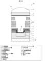
図1は実施形態1に係る固体撮像装置18に配列された画素21の構成を示す図である。図2は、実施形態1に係る固体撮像装置18の画素21の構造断面図である。図3は画素21の平面図である。FIG. 1 is a diagram showing the configuration of
固体撮像装置18は、基板19を備える。基板19は、半導体基板1と、半導体基板1の上に形成されたエピタキシャル層2とを含む。The solid-
固体撮像装置18は、基板19の上に行列状に配列された複数の画素21を備える。各画素21は、基板19に入射する光を電荷に変換するための光電変換領域3と、光電変換領域3で変換された電荷を保持するための電荷保持領域4と、光電変換領域3に形成された光電変換素子に蓄積した信号電荷を電圧に変換したり、画素をリセット及び選択したりする為に必要なトランジスタが形成される画素トランジスタ領域17とを含む。The solid-
光電変換領域3は、基板19に入射する光を電荷に変換するためにエピタキシャル層2の内部に配置される。電荷保持領域4は、エピタキシャル層2の内部の光電変換領域3よりも光の入射側に配置される。The
各画素21は、エピタキシャル層2の光の入射側の表面から光電変換領域3に向かって少なくとも電荷保持領域4に対応する深さまで掘り込まれた掘り込み領域20と、電荷保持領域4への光の到達を遮るために、電荷保持領域4のエピタキシャル層2の表面側を覆って掘り込み領域20の側壁を延伸するように形成された遮光膜8とを備える。Each
各画素21は、電荷を光電変換領域3から電荷保持領域4へ転送するための電荷転送ゲート電極6をさらに備える。光電変換領域3により光から変換された電荷は、光電変換領域3から電荷転送ゲート電極6を経由して電荷保持領域4に到達する電荷転送経路を通って電荷保持領域4へ転送される。Each
電荷転送経路とは、何れの実施形態においても、光電変換領域3と電荷転送ゲート電極6とがオーバーラップする領域(正確には電荷転送ゲート電極6がオン時の光電変換領域3のポテンシャルの最も深い領域)から電荷保持領域4のポテンシャルの最も深い領域までの経路を意味する。In any embodiment, the charge transfer path refers to the path from the region where the
電荷保持領域4まで電荷を転送した後は、いわゆる一般的なローリングシャッター方式のCIS(CMOS Image Sensor)と動作は同じである。即ち、電荷保持領域4からフローティングディフュージョン(FD)に電荷が転送される前にFDをリセットトランジスタによりリセットし、リセット時のFDの電荷をソースフォロアトランジスタにより電圧に変換する。そして、セレクトトランジスタにより検出画素を選択することでリセット信号をアナログ-デジタル変換(AD変換)し、ラッチ回路により取得する。その後、すぐに電荷保持領域4に蓄積していた光信号電荷をFDに転送し、FDに転送された電荷をソースフォロアトランジスタより電圧に変換する。そして、オン状態のセレクトトランジスタを介して光信号とリセット信号とをAD変換しラッチ回路より取得する。その後、デジタル回路によって光信号及びリセット信号からリセット信号を引き算することで光電変換により生じた信号を正しく取得することができる。After the charge is transferred to the
図2及び図3に示すように、電荷転送ゲート電極6が光電変換領域3のポテンシャルの深い部分と電荷保持領域4との両方にオーバーラップしている。このため、光電変換領域3から電荷保持領域4に電荷を転送する電荷転送経路が形成される。As shown in Figures 2 and 3, the charge
電荷転送ゲート電極6がオンの時、電荷転送ゲート電極6下に電界が印加され、電荷転送ゲート電極6下のポテンシャルが深い側に変調する。この時、エピタキシャル層2の表面の方が電界による影響を強く受け、さらに不純物注入とレイアウトによって形成された電荷保持領域4のポテンシャルスロープはこの時も引き継がれ、電荷転送ゲート電極6がオフの時のポテンシャルにオフセット分だけ深くなったポテンシャル形状となる。When the charge
したがって、電荷転送ゲート電極6がオンの時に光電変換領域3のポテンシャルの最も深い領域が、光電変換領域3と電荷転送ゲート電極6とがオーバーラップする領域下に形成される。そして、そこから電荷転送ゲート電極6で変調した分、光電変換領域3のポテンシャルの最も深い領域より、もっと深い電荷保持領域4のポテンシャルスロープに沿って、電荷保持領域4のポテンシャルの最も深い領域まで電荷は移動する。Therefore, when the charge
光電変換領域3は、掘り込み領域20の下側から電荷保持領域4の下側まで延伸して形成される。光電変換領域3上の堀り込み領域20は電荷保持領域4よりも深い位置まで掘り込まれて形成されている。この時、電荷は、電荷保持領域4の下方の光電変換領域3からその直上の電荷保持領域4に垂直に転送される。そして、電荷が垂直に転送される箇所の光電変換領域3と電荷保持領域4との間の距離を適切に構成するために、電荷保持領域4に向かって突出する突出部分が光電変換領域3に形成されている。光電変換領域3の直上の掘り込み領域20の掘り込み深さ次第では、突出部分が形成されない場合もあるし、逆に、電荷が垂直に転送される箇所の光電変換領域3と電荷保持領域4との間の距離を保たなくてはならない場合もある。この転送部の光電変換領域3と電荷保持領域4との間のおおよその距離は0.35μm~0.45μm程度であり得る。The
エピタキシャル層2の上に絶縁膜5が形成される。An
電荷転送ゲート電極6は、絶縁膜5の上に形成されて掘り込み領域20の側壁を掘り込み領域20の底に到達するまで延伸する。The charge
基板19に入射する光のロスを低減する反射防止膜7が、電荷転送ゲート電極6の上、及び掘り込み領域20の上に形成される。遮光膜8は、反射防止膜7の上に形成される。An
遮光膜8は、タングステン単層より光反射率が高くなる単数又は複数の膜構造で形成されている。The light-shielding
各画素21は、遮光膜8上に設けられ、複数の金属配線が形成された少なくとも1層の配線層10と、遮光膜8の上に形成された層間絶縁膜9とを備えている。Each
半導体基板1としては、公知の半導体基板が用いられ、例えばシリコン基板を用いることができる。光電変換領域3は、入射した光を電荷に変換できる構造を有していればよく、例えばフォトダイオードにより構成される。行列状に配列された複数の画素21において、図1に示すように、行方向に沿って互いに隣接する光電変換領域3の間に電荷保持領域4が設けられている。例えば、電荷保持領域4は、エピタキシャル層2内のn型層で構成されており、光電変換領域3と電荷保持領域4との間には、ポテンシャルバリアが形成されている。As the
また、光電変換領域3の上方には、掘り込み領域20が形成されている。電荷保持領域4の上側および掘り込み領域20の側壁には遮光膜8が配置されている。また、電荷転送ゲート電極6は、エピタキシャル層2および絶縁膜5を介して電荷保持領域4の上面および側面を覆うように配置されている。A recessed
本実施形態の固体撮像装置18は、配線層10上および層間絶縁膜9上を覆い、層間絶縁膜9よりも高い屈折率を有するパッシベーション膜12と、パッシベーション膜12上に設けられた平坦化膜13と、平坦化膜13上に光電変換領域3を覆うように配置されたマイクロレンズ15とを備えている。The solid-
パッシベーション膜12は、窒化シリコン系材料で構成されていてもよく、層間絶縁膜9は酸化シリコン系材料で構成されていてもよい。なお、窒化シリコン系材料とは、窒化シリコンを主成分とする材料を意味し、任意の不純物等が含まれていてもよい。また、酸化シリコン系材料とは、酸化シリコンを主成分とする材料を意味し、ここでは、絶縁性を有する限り、酸化シリコンに任意の不純物等が含まれていてもよい。The
図2に示すように、本実施形態の固体撮像装置18に入射した光は、マイクロレンズ15によってマイクロレンズ15の中心軸方向に屈折して平坦化膜13およびパッシベーション膜12に入射する。その後、光は層間絶縁膜9を通過して光電変換領域3へと入射する。光電変換領域3に入射した光は、電荷へと変換される。この光電変換によって生じた電荷は、電荷転送ゲート電極6への電圧印加によって電荷保持領域4へと転送される。電荷保持領域4に蓄積された電荷は、画像信号として利用され、信号処理により撮像画像を構成する。なお、本実施形態の固体撮像装置18は、グローバルシャッター方式を採用しているので、光電変換領域3での光電変換および光電変換領域3から電荷保持領域4への電荷の転送は、全ての画素について同じタイミングで行われる。2, the light incident on the solid-
上述の光電変換の際に、電荷保持領域4に直接光が入射すると、寄生光感度ノイズが発生する。これは、電荷保持領域4においても光電変換を生じてしまうためである。When light is directly incident on the
電荷保持領域4は、Siを含むエピタキシャル層2中にAsやPhなどのドナーを不純物注入により形成し、それにより形成された主に表面部のpnジャンクション容量により電荷を保持する。すなわち、光電変換領域3に形成されるフォトダイオードと同様に、電荷保持領域4は光が入射すると光電変換によりキャリアを発生させる。The
また、直接電荷保持領域4に光が入射しなくても、電荷保持領域4の下方のp領域(画素分離領域)で光電変換された電荷が拡散により電荷保持領域4に到達する成分もある。Even if light does not directly strike the
そこで、電荷保持領域4に光が入射するのを防ぐために、電荷転送ゲート電極6の上面および側面に遮光膜8が設けられている。この遮光膜8の構成材料としては、タングステン等の金属が用いられる。タングステンは、光の吸収係数が大きく、薄い膜厚でも高い遮光能力を有するので、遮光膜の材料としては好ましい。To prevent light from entering the
図4は比較例に係る固体撮像装置の画素の構造断面図である。図5は他の比較例に係る固体撮像装置の画素の構造断面図である。Figure 4 is a cross-sectional view of the structure of a pixel of a solid-state imaging device according to a comparative example. Figure 5 is a cross-sectional view of the structure of a pixel of a solid-state imaging device according to another comparative example.
掘り込み領域20は、図2で前述した実施形態1の固体撮像装置18と異なり、電荷保持領域4よりも浅い位置までしかエピタキシャル層2に掘り込まれていない。そして、光電変換領域3の上面と電荷保持領域4の上面とがエピタキシャル層2内に同じ深さで配置されている。遮光膜8は、電荷転送ゲート電極6を覆うように配置される。Unlike the solid-
図4に示す固体撮像装置は、カラーフィルタ14および光導波路11を有している。カラーフィルタ14は、入射した光を赤、緑、青に着色させてそれぞれの色素毎の光を光電変換領域3において電気信号に置き換えるための機能を有する。光導波路11は、入射した光を画素21の中心軸に集光させて、光電変換領域3に効率よく入射させる機能を有する。図5に示す固体撮像装置は、インナーレンズ16と上記カラーフィルタ14とを有している。The solid-state imaging device shown in FIG. 4 has a
このような図4及び図5に示す比較例の固体撮像装置の構造では、基板19に入射する光は、光電変換領域3だけでなく、電荷保持領域4にも入射するため、電荷保持領域4においても光電変換が生じてしまう。これにより、比較例の固体撮像装置では、光電変換領域3で光電変換された電荷以外の電荷が1フレーム前の信号電荷を保持している電荷保持領域4に蓄積されることになり、寄生光感度ノイズが生じることになる。In the structure of the comparative solid-state imaging device shown in Figures 4 and 5, the light incident on the
これに対して、本実施形態の固体撮像装置18は、光電変換領域3を電荷保持領域4の位置から半導体基板1側へ後退させて、電荷保持領域4の下面に沿って光電変換領域3を延伸させている。光電変換領域3を半導体基板1側に後退させて生じた空いたスペースに、掘り込み領域20を形成している。In contrast, in the solid-
掘り込み領域20の側壁は、電荷保持領域4の側面と対向している。遮光膜8は、反射防止膜7および電荷転送ゲート電極6を介して、電荷保持領域4のエピタキシャル層2の表面側を覆って掘り込み領域20の側壁を延伸するように形成される。The sidewalls of the recessed
このような構成を採用することで、層間絶縁膜9を通過してエピタキシャル層2に入射した光は遮光膜8によって遮られて電荷保持領域4に入射できなくなる。これによって、電荷保持領域4における光電変換が生じなくなり寄生光感度ノイズが発生しなくなる。By adopting such a configuration, light that passes through the
さらに、光電変換領域3は、電荷保持領域4の下側まで拡張させたことで、電荷保持領域4の下方のp領域(画素分離領域)で光電変換された電荷が拡散により電荷保持領域4に到達する成分を限りなく低減させるだけでなく、飽和容量を向上させることができる。そして、寄生光感度ノイズの消滅によって、本実施形態の固体撮像装置18は感度やF値特性(斜入射特性)の向上及びシェーディング抑制の為だけに基板上の集光構造を最適化できる。Furthermore, by extending the
集光構造を決定する時、感度と寄生光感度ノイズとがトレードオフの関係になってしまうことがしばしばある。例えば、光電変換領域3上の遮光膜8の開口を広くすれば、感度が向上するが寄生光感度ノイズは悪化する。逆に、開口を狭くすれば感度は減少するが寄生光感度ノイズは改善する。When determining the light collection structure, there is often a trade-off between sensitivity and parasitic photosensitivity noise. For example, widening the opening of the light-shielding
実際に集光構造を設計する時には、感度と寄生光感度ノイズとのバランスがとれる開口で設計される。ところが、本実施形態に係る集光構造では寄生光感度ノイズは原理的に発生しない。このため、遮光膜8の開口は製造限界まで広げることができるので、制限なく感度を向上するための集光構造を設計することができる。When actually designing a light-collecting structure, the opening is designed to balance the sensitivity and parasitic photosensitivity noise. However, in the light-collecting structure of this embodiment, parasitic photosensitivity noise does not occur in principle. Therefore, the opening of the light-shielding
また、感度と寄生光感度ノイズとの間のトレードオフ、または、シェーディング(撮像する際はレンズを介してCMOSイメージセンサーに光が入射されるため画面端の画素は角度のついた光が入射するので、一般に画面中央の画素よりも、画面端の画素の方が感度が落ちる感度のばらつきの現象)と寄生光感度ノイズとの間のトレードオフを気にせずに集光構造を決定することができる。このため、本実施形態に係る固体撮像装置18の集光構造は感度(光学特性)を向上させることができる。In addition, the light-collection structure can be determined without having to worry about the trade-off between sensitivity and parasitic photosensitivity noise, or between shading (a phenomenon of variation in sensitivity in which pixels at the edges of the screen generally have lower sensitivity than pixels in the center of the screen because light is incident on the CMOS image sensor through a lens when capturing an image, resulting in angled light incident on the pixels at the edges of the screen) and parasitic photosensitivity noise. Therefore, the light-collection structure of the solid-
比較例に係る図4及び図5に示す構造の場合、光電変換領域3と電荷保持領域4とのポテンシャルの深い部分(電荷蓄積の主要部分)はどちらもSiを含むエピタキシャル層2の最表面に位置するので、一定の距離離すようにレイアウトしなければならない。接近すると短チャネル化が起こり飽和容量が著しく減少するからである(光電変換領域3と電荷保持領域4の空乏層とが繋がることに起因する)。接近すると、それだけではなく、電荷保持領域4側に溢れるブルーミングが著しく劣化してしまう。したがって、上記のように光電変換領域3と電荷保持領域4とが接近しないように各画素21のレイアウトの大きさが制限されてしまう。また、画素21の画素トランジスタ領域17内の画素トランジスタ(フローティングディフュージョン(FD))に転送された電子を排出するリセットトランジスタ、電荷を電位に変換するソースフォロアトランジスタ、電子シャッターの役割である電荷排出用トランジスタ、セレクト有りの画素構造であれば、画素を選択するセレクトトランジスタはSiを含むエピタキシャル層2最表面に存在し、普通、画素トランジスタの周りはシャロートレンチアイソレーション(STI)で囲み光電変換領域3や電荷保持領域4から分離する。これは、画素トランジスタには濃度の高い不純物注入を行うため、空乏層の伸びが大きく、かなり距離をとらないと光電変換領域3などのN型領域と空乏層が繋がってしまい、リーク源となってしまうからである。STIを形成すれば、空乏層はSTIの下を周りこまなければならないので、画素トランジスタと光電変換領域3との間の距離をSTIの幅までは近づけることができる。このように、画素トランジスタによっても光電変換領域3のレイアウトサイズは制限されてしまう。In the comparative example shown in the structure of Figures 4 and 5, the deep potential parts (main charge storage parts) of the
これに対して、図2に示される固体撮像装置18に形成された光電変換領域3の電荷蓄積の主要部分(ポテンシャルの深い部分、この部分はなるべく電荷保持領域4に寄せたい)は、電荷保持領域4にも画素トランジスタにも影響されない深さに位置している。このため、この光電変換領域3は、隣接する画素21に形成された光電変換領域3(隣接フォトダイオード)との画素分離が十分できる大きさまでは拡大することができる。したがって、比較例よりも大幅に光電変換領域3の飽和領域を拡大することができる。In contrast, the main portion of the charge accumulation in the
図6は実施形態1に係る固体撮像装置18に設けられた遮光膜8の波長に対する反射率のスペクトルを示すグラフである。Figure 6 is a graph showing the spectrum of reflectance versus wavelength for the light-shielding
遮光膜8のタングステン(W)単層より光反射率が高くなる単数の膜構造としては、例えば、アルミニウム(Al)/窒化チタン(TiN)の膜構造、銅(Cu)/タンタル(Ta)の膜構造、W/TiNの膜構造、TiN/Ti/W/TiNの膜構造が挙げられる。Examples of single film structures that have a higher light reflectance than the single layer of tungsten (W) of the light-shielding
図6のグラフは、上記各膜構造における反射率スペクトルをシミュレーションした結果を示している。Al/TiNの膜構造、Cu/Taの膜構造の方が、どの波長領域においても、タングステン単層の膜構造よりも反射率が大幅に高いことが分かる。従って、反射率のみを考慮すれば、Al、Cuの方が、遮光膜8の材料としてはWよりも適切である。ただし、Cu製膜プロセスは遮光膜配線用の溝を形成後、Cuが絶縁膜中へ拡散することを防止するため、TaやTaNなどの安定な金属・金属化合物を絶縁膜上に製膜し、遮光膜配線溝にCuを埋め込んだ後、化学的機械研磨(CMP)により不要な部分を除去・平坦化するというプロセスフローでしか形成できない為、製造プロセス的な制約を受ける。すなわち、遮光膜構造の自由度が小さくなる。また、Cuが絶縁膜中や基板表面へ拡散してしまうと、金属汚染起因の白傷ピークを悪化させるなどデバイス特性を著しく劣化させる。このような理由から、実際遮光膜にCuは採用されていない。The graph in Figure 6 shows the results of simulating the reflectance spectrum for each of the above film structures. It can be seen that the Al/TiN film structure and the Cu/Ta film structure have significantly higher reflectance than the single-layer tungsten film structure in all wavelength regions. Therefore, if only the reflectance is considered, Al and Cu are more suitable materials for the light-shielding
また、信頼性等の観点から、遮光膜8はタングステン単層よりも絶縁膜上のTiN膜上にWを製膜するW/TiNの膜構造の方が好ましい。W/TiN膜構造の反射率スペクトルはW単層の反射率スペクトルとほとんど一致している。さらに、W/TiN膜上にTiN/Ti膜を形成することで反射率を高めることができる。ただし、この時の副作用として、Tiの水素吸蔵の性質が基板の界面準位の水素終端効果を妨害する方向に働き、暗時特性を悪化させてしまう可能性がある。In terms of reliability, the light-shielding
図7は実施形態1に係る固体撮像装置18に設けられたパッシベーション膜12の応力と暗電流との間の関係を示すグラフである。Figure 7 is a graph showing the relationship between the stress of the
パッシベーション膜12は、-5.0×10⁻⁹dyne/cm2以下のコンプレッシブ方向のストレスを有することが好ましい。パッシベーション膜12の膜質を変化させると、屈折率も変化するが、パッシベーション膜12がコンプレッシブ方向のストレスを持ち、イメージセンサー(固体撮像装置18の基板19)の反り(イメージセンサー全体にかかる応力)を、-5.0×10-9dyne/cm2以下に調節することができる。 The
これにより、光導波路11を導入することによる副作用をカバーすることができる。光導波路11は他の周辺の部材の材料と比較して熱収縮率が圧倒的に大きく、これにより暗電圧を悪化させる方向に働く応力がSiを含む基板19に伝搬する。そこで、イメージセンサーにかかる反りを暗電流に良い方向に調節するようにパッシベーション膜12の膜質を決定することが重要になってくる。This makes it possible to cover up the side effects of introducing the
パッシベーション膜12のストレスをコンプレッシブ方向に制御すると、パッシベーション膜12のコンプレッシブ方向のストレスが、光電変換領域3を含むエピタキシャル層2の表面のシリコンまで伝搬することにより、光電変換領域3を含むエピタキシャル層2の表面のシリコンのバンドギャップは大きくなる。このバンドギャップが大きくなると、暗電流は指数関数的に低減される。When the stress of the
図7に示すように、コンプレッシブ方向のストレスが-5.0×10⁻⁹dyne/cm2以下で暗電流の変化が緩やかになっていることから、-5.0×10-9dyne/cm2以下にパッシベーション膜12のコンプレッシブ方向のストレスを設定すると、暗電流を指数関数的に低減することができる。 As shown in FIG. 7, the change in dark current is gradual when the compressive stress is −5.0×10⁻⁹ dyne/cm2 orless. Therefore, by setting the compressive stress of the
〔実施形態1の変形例1〕
図8は、実施形態1の変形例1に係る固体撮像装置18Aの画素21の構造断面図である。 [
FIG. 8 is a cross-sectional view of the structure of a
実施形態1の固体撮像装置18との違いは、パッシベーション膜12と平坦化膜13との間に光導波路11が配置されていることである。その他の構造および作用効果については、実施形態1の固体撮像装置18と同じであるので説明は省略する。The difference from the solid-
固体撮像装置18Aに光導波路11を配置することによってマイクロレンズ15に入射した光は平坦化膜13を透過して光導波路11に入射する。光導波路11では、入射した光が基板19に対して垂直方向の中心軸に集光させられる。集光した入射光は、光導波路11を出射して、層間絶縁膜9を透過して光電変換領域3に入射する。By disposing the
このように、光導波路11は光電変換領域3に、光を集光して入射させるので、光導波路11が配置されない構成に比べて、光電変換領域3に入射する光量を増加させることができる。本実施形態の固体撮像装置18Aは、感度をより高くすることができる。In this way, the
表面照射型(FSI : Front side illumination)の構造においては、光入射側に配線層10が配置され、マイクロレンズ15で集めた光の一部が配線層10により遮られロスとなってしまう(メタルけられ)。さらに、グローバルシャッターCISでは、画素21内に電荷保持領域4(メモリーノード)も形成しなければならない為、画素面積に対する光電変換領域3(フォトダイオード部)の開口率(フィルファクター)がより小さくなってしまう。結果として、感度やF値特性(斜入射特性)、シェーディング特性が劣化してしまう。In a front side illumination (FSI) structure, the
その解決手段として、光導波路構造があり、光導波路11は、層間絶縁膜9よりも屈折率の高い材料を用いることにより光を閉じ込める効果を発揮する。すなわち、マイクロレンズ15から集光した光は光導波路11の入り口(上側開口)に入射さえすれば、周りに漏れることなく出口(下側開口)から照射されるので、マイクロレンズ15に入射した光を効率よく光電変換領域3まで導くことができる。One solution to this problem is the optical waveguide structure, where the
光電変換領域3の直上を掘りこみ、マイクロレンズ15から基板19までの距離が遠くなっている本実施形態の構成において、光導波路11は特に効果を発揮する。掘り込み領域20まで光導波路11により入射光を導きさえすれば、どんな方向で光導波路11から出てきた光が基板19上に入射しようが寄生光感度ノイズ(PLS)は起こらない。このため、光導波路11のテーパー角を気にすることなく設計できるので、自由度が増し感度やF値特性、シェーディングを向上させやすい。In the configuration of this embodiment, where the area directly above the
〔実施形態1の変形例2〕
図9は、実施形態1の変形例2に係る固体撮像装置18Bの画素21の構造断面図である。 [
FIG. 9 is a cross-sectional view of the structure of a
実施形態1の固体撮像装置18との違いは、平坦化膜13とマイクロレンズ15の間にカラーフィルタ14が配置されていることである。その他の構造および作用効果については、実施形態1の固体撮像装置18と同じであるので説明は省略する。The difference from the solid-
固体撮像装置18Bにカラーフィルタ14を配置することによって、マイクロレンズ15に入射した光はカラーフィルタ14で特定の波長の光のみ透過し、それ以外の光はカラーフィルタ14で吸収される。したがって、特定の波長の光のみ光電変換領域3に入射して光電変換される。By disposing a
このように、本実施形態の固体撮像装置18Bは、画素21ごとに透過する光の波長を変えたカラーフィルタ14を配置することで、光の3原色である赤色、緑色、青色の光を画素21ごと電気信号に変換させることができる。赤色、緑色、青色の3色の光を電気信号に変換後、再び電気信号を光に変換すれば、カラー画像を表示することができる。In this way, the solid-
〔実施形態1の変形例3〕
図10は、実施形態1の変形例3に係る固体撮像装置18Cの画素21の構造断面図である。 [
FIG. 10 is a cross-sectional view of the structure of a
実施形態1の固体撮像装置18との違いは、パッシベーション膜12と平坦化膜13との間に光導波路11を配置し、平坦化膜13とマイクロレンズ15との間にカラーフィルタ14が配置されていることである。その他の構造および作用効果については、実施形態1の固体撮像装置18と同じであるので説明は省略する。The difference with the solid-
本実施形態の固体撮像装置18Cは、実施形態1の変形例1と変形例2とを組み合わせたものである。固体撮像装置18Cにカラーフィルタ14を配置することによって、マイクロレンズ15に入射した光はカラーフィルタ14で特定の波長の光のみ透過し、それ以外の光はカラーフィルタ14で吸収される。カラーフィルタ14を透過した特定の波長の光は平坦化膜13を透過して光導波路11に入射する。光導波路11では、入射した特定の波長の光が基板19に対して垂直方向の中心軸に集光させられる。集光した特定の波長の入射光は、光導波路11を出射して、層間絶縁膜9を透過して光電変換領域3に入射する。The solid-
このように、本実施形態の固体撮像装置18Cは、特定の波長の光のみを取り出して、光電変換領域3に入射する光量を増加させることができる。光導波路11とカラーフィルタ14とを固体撮像装置18Cに配置することで、感度のより高いカラー画像を表示することが可能となる。In this way, the solid-
〔実施形態1の変形例4〕
図11は、実施形態1の変形例4に係る固体撮像装置18Dの画素21の構造断面図である。 [Fourth Modification of First Embodiment]
FIG. 11 is a cross-sectional view of the structure of a
実施形態1の固体撮像装置18との違いは、パッシベーション膜12と平坦化膜13との間にインナーレンズ16を配置していることである。その他の構造および作用効果については、実施形態1の固体撮像装置18と同じであるので説明は省略する。The difference from the solid-
固体撮像装置18Dに、インナーレンズ16を配置したことによって、マイクロレンズ15を透過した入射光は、平坦化膜13を透過してインナーレンズ16に入射して基板19と垂直方向の中心軸に向けて集光する。集光した入射光は、パッシベーション膜12および層間絶縁膜9を透過して光電変換領域3に入射する。インナーレンズ16を配置することによって、外からの入射光を集光して、光電変換領域3に入射させることができる。By disposing the
これによって、外からの入射光を効率的に光電変換領域3で電子に変換することができるので、感度をより向上させることができる。This allows external incident light to be efficiently converted into electrons in the
前述したように、FSI型のグローバルシャッターCISはフィルファクターの減少により集光率が悪化してしまうことが課題となる。前述した光導波路構造の他に、このようなインナーレンズ16を用いて、マイクロレンズ15から入射した光を効率よく基板19に集光することができる。As mentioned above, a problem with FSI-type global shutter CIS is that the light collection rate deteriorates due to a decrease in the fill factor. In addition to the optical waveguide structure described above, by using this type of
〔実施形態1の変形例5〕
図12は、実施形態1の変形例5に係る固体撮像装置18Eの画素21の構造断面図である。 Fifth Modification of the First Embodiment
FIG. 12 is a structural cross-sectional view of a
実施形態1の固体撮像装置18との違いは、パッシベーション膜12と平坦化膜13との間にインナーレンズ16を配置し、平坦化膜13とマイクロレンズ15との間にカラーフィルタ14が配置されていることである。その他の構造および作用効果については、実施形態1の固体撮像装置18と同じであるので説明は省略する。The difference with the solid-
本実施形態の固体撮像装置18Eは、実施形態1の変形例2と変形例4とを組み合わせたものである。固体撮像装置18Eにカラーフィルタ14を配置することによって、マイクロレンズ15に入射した光はカラーフィルタ14で特定の波長の光のみ透過し、それ以外の光はカラーフィルタ14で吸収される。カラーフィルタ14を透過した特定の波長の光は平坦化膜13を透過してインナーレンズ16に入射する。インナーレンズ16では、入射した特定の波長の光は基板19に対して垂直方向の中心軸に集光させられる。集光した特定の波長の入射光は、インナーレンズ16を出射して、層間絶縁膜9を透過して光電変換領域3に入射する。The solid-
このように、本実施形態の固体撮像装置18Eは、特定の波長の光のみを取り出して、光電変換領域3に入射する光の光量を増加させることができる。インナーレンズ16とカラーフィルタ14とを固体撮像装置18Eに配置することで、感度のより高いカラー画像を表示することが可能となる。In this way, the solid-
〔実施形態1の変形例6〕
図13は実施形態1の変形例6に係る固体撮像装置18Fの画素21の構造断面図である。 [Sixth Modification of the First Embodiment]
FIG. 13 is a structural cross-sectional view of a
実施形態1の固体撮像装置18との違いは、パッシベーション膜12と平坦化膜13との間に光導波路11及びインナーレンズ16が配置されていることである。その他の構造および作用効果については、実施形態1の固体撮像装置18と同じであるので説明は省略する。The difference from the solid-
マイクロレンズ15に入射した光は、平坦化膜13を透過してインナーレンズ16に入射して基板19と垂直方向の中心軸に向けて集光する。集光した入射光は、光導波路11に入射する。光導波路11では、入射した特定の波長の光が基板19に対して垂直方向の中心軸に集光させられる。集光した特定の波長の入射光は、光導波路11を出射して、層間絶縁膜9を透過して光電変換領域3に入射する。Light incident on the
〔実施形態1の変形例7〕
図14は実施形態1の変形例7に係る固体撮像装置18Gの画素21の構造断面図である。 [Seventh Modification of the First Embodiment]
FIG. 14 is a structural cross-sectional view of a
実施形態1の固体撮像装置18との違いは、パッシベーション膜12と平坦化膜13との間に光導波路11及びインナーレンズ16が配置され、平坦化膜13とマイクロレンズ15との間にカラーフィルタ14が配置されていることである。その他の構造および作用効果については、実施形態1の固体撮像装置18と同じであるので説明は省略する。The difference with the solid-
マイクロレンズ15に入射した光は、カラーフィルタ14で特定の波長の光のみ透過し、それ以外の光はカラーフィルタ14で吸収される。カラーフィルタ14を透過した特定の波長の光は平坦化膜13を透過してインナーレンズ16に入射する。インナーレンズ16では、入射した特定の波長の光は基板19に対して垂直方向の中心軸に集光させられる。集光した特定の波長の入射光は、インナーレンズ16を出射して、光導波路11に入射する。光導波路11では、入射した特定の波長の光が基板19に対して垂直方向の中心軸に集光させられる。集光した特定の波長の入射光は、光導波路11を出射して、層間絶縁膜9を透過して光電変換領域3に入射する。Of the light incident on the
〔実施形態1の変形例8〕
図15は実施形態1の変形例8に係る固体撮像装置18Hの画素21の構造断面図である。図16は図15に示される線ABに沿った断面図である。図17は画素21の平面図である。 [Eighth Modification of First Embodiment]
Fig. 15 is a structural cross-sectional view of a
実施形態1の固体撮像装置18との違いは、電荷転送ゲート電極6Hが、電荷保持領域4の両側面を覆って電荷保持領域4を挟むようにエピタキシャル層2に埋め込まれていることである。その他の構造および作用効果については、実施形態1の固体撮像装置18と同じであるので説明は省略する。The difference with the solid-
固体撮像装置18Hに入射した光は、マイクロレンズ15によってマイクロレンズ15の中心軸方向に屈折されて平坦化膜13およびパッシベーション膜12に入射する。その後、当該光は層間絶縁膜9を通過して光電変換領域3へと入射する。Light incident on the solid-
光電変換領域3に入射した光は、電荷へと変換される。この光電変換によって生じた電荷は、電荷転送ゲート電極6Hへの電圧印加によって電荷保持領域4へと転送される。Light incident on the
図15~図17に示すように、電荷転送ゲート電極6Hが光電変換領域3のポテンシャルの深い部分と電荷保持領域4との両方にオーバーラップしている。このため、光電変換領域3から電荷保持領域4に電荷を転送する電荷転送経路が形成される。As shown in Figures 15 to 17, the charge
このように、電荷保持領域4の両側面を覆って電荷保持領域4を挟むようにエピタキシャル層2に電荷転送ゲート電極6Hを埋め込んでしまえば、掘り込み領域20の側壁と電荷保持領域4との間に電荷転送ゲート電極6Hが形成されていなくても、光電変換領域3から電荷保持領域4への電荷の転送が可能になる。In this way, if the charge
このような電荷転送ゲート電極6Hの埋め込み構造は、光電変換領域3から電荷保持領域4への電荷の転送に有利なポテンシャルを形成しやすい。これにより、掘り込み領域20の側壁と電荷保持領域4との間に電荷転送ゲート電極6Hが存在しない分だけ、掘り込み領域20の側壁を延伸する遮光膜8の開口寸法を拡大することができる。従って、光電変換領域3の集光率が高められ、固体撮像装置18Hの感度が向上する。This buried structure of the charge
このように、Siをシャロートレンチアイソレーション(STI)と同じようにエッチングし、ポリシリコンゲート電極をエピタキシャル層2に埋め込むことにより、電荷保持領域4の両横に電荷転送ゲート電極6Hを埋め込み、電荷保持領域4の両横から挟むように電圧を電荷保持領域4に印加し、電荷転送をアシストするように構成される。In this way, by etching the Si in the same way as shallow trench isolation (STI) and embedding polysilicon gate electrodes in the
なお、図16及び図17では両横から電荷保持領域4を電荷転送ゲート電極6Hで挟み込む構造を示しているが、電荷保持領域4の片側だけに電荷転送ゲート電極6Hを設けてもよい。Note that although Figures 16 and 17 show a structure in which the
〔実施形態2〕
本発明の他の実施形態について、以下に説明する。なお、説明の便宜上、上記実施形態にて説明した部材と同じ機能を有する部材については、同じ符号を付記し、その説明を繰り返さない。 [Embodiment 2]
Other embodiments of the present invention will be described below. For ease of explanation, the same reference numerals are given to members having the same functions as those described in the above embodiment, and the description thereof will not be repeated.
図18は実施形態2に係る固体撮像装置18Iの画素21の構造断面図である。実施形態1の固体撮像装置18との違いは、光電変換領域3の直上の掘り込み領域20の深さが電荷保持領域4の下端の深さよりも浅いこと、及び、光電変換領域3が掘り込み領域20の下側にのみ形成され、電荷保持領域4の下側に延伸していないことである。Figure 18 is a structural cross-sectional view of a
電荷保持領域4まで光電変換領域3を伸ばすと、光電変換領域3と電荷保持領域4とが繋がってしまうため、光電変換領域3を電荷保持領域4まで拡大することができず、このような構成になっている。If the
電荷転送ゲート電極6は、電荷保持領域4を覆うようにエピタキシャル層2の上に形成され、掘り込み領域20の側壁を延伸して底面に到達し、底面の一部を延伸して。光電変換領域3及び電荷保持領域4とオーバーラップする。The charge
電荷転送ゲート電極6に電圧が印加されると、光電変換領域3により変換された電荷は、光電変換領域3から電荷転送ゲート電極6を通って電荷保持領域4に転送される。When a voltage is applied to the charge
〔実施形態2の変形例8〕
図19は実施形態2の変形例に係る固体撮像装置18Jの画素21の構造断面図である。実施形態2の固体撮像装置18Iとの違いは、光電変換領域3(フォトダイオード)の深い側の領域を電荷保持領域4(メモリーノード)の下側まで拡張していることである。 [Eighth Modification of the Second Embodiment]
19 is a structural cross-sectional view of a
この光電変換領域3は、深い側から浅い側にポテンシャルスロープが形成され、深い側で発生した電荷も浅い側に流れ、蓄積されるように不純物注入が調節される。これにより、光電変換領域3の飽和容量を図18に示す構成よりも拡大することができる。In this
〔まとめ〕
本発明の態様1に係る固体撮像装置18・18A~18Jは、基板19に複数の画素21が行列状に配列された固体撮像装置18・18A~18Jであって、前記複数の画素21のそれぞれが、前記基板19に入射する光を電荷に変換するために前記基板19の内部に配置された光電変換領域3と、前記光電変換領域3で変換された電荷を保持するために前記基板19の内部の前記光電変換領域3よりも前記光の入射側に配置された電荷保持領域4と、前記基板19の前記光の入射側の表面から前記光電変換領域3に向かって少なくとも前記電荷保持領域4に対応する深さまで掘り込まれた掘り込み領域20と、前記電荷保持領域4の前記基板19の前記表面側を覆って前記掘り込み領域20の側壁を延伸するように形成された遮光膜8とを備えている。 〔summary〕
Solid-
上記の構成によれば、光電変換領域で変換された電荷を保持するための電荷保持領域が基板の内部の光電変換領域よりも光の入射側に配置される。そして、基板の光の入射側の表面から掘り込まれる掘り込み領域が光電変換領域に向かって少なくとも電荷保持領域に対応する深さまで配置される。また、光の電荷保持領域への到達を遮るための遮光膜が電荷保持領域の基板の表面側を覆って掘り込み領域の側壁を延伸するように形成される。According to the above configuration, a charge retention region for retaining charges converted in the photoelectric conversion region is disposed on the light incident side of the photoelectric conversion region inside the substrate. A recessed region that is recessed from the surface of the substrate on the light incident side is disposed toward the photoelectric conversion region to a depth at least corresponding to the charge retention region. In addition, a light-shielding film for blocking light from reaching the charge retention region is formed so as to cover the surface side of the substrate of the charge retention region and extend along the sidewall of the recessed region.
このため、電荷保持領域の上面だけでなく電荷保持領域の側面も遮光膜により覆われる。この結果、基板の中に入射した光のうち電荷保持領域に回折して漏れこむ光に起因する寄生光感度ノイズが原理的に発生しない固体撮像装置を提供することができる。For this reason, not only the top surface of the charge retention region but also the side surface of the charge retention region are covered with the light-shielding film. As a result, it is possible to provide a solid-state imaging device that, in principle, does not generate parasitic photosensitivity noise caused by light that is diffracted and leaks into the charge retention region out of the light that enters the substrate.
本発明の態様2に係る固体撮像装置18・18A~18Jは、上記態様1において、前記電荷を前記光電変換領域3から前記電荷保持領域4へ転送するための電荷転送ゲート電極6・6Hをさらに備え、前記電荷は、前記光電変換領域3から前記電荷転送ゲート電極6・6Hを経由して前記電荷保持領域4に到達する電荷転送経路を通って前記電荷保持領域4へ転送されることが好ましい。The solid-
上記の構成によれば、電荷転送ゲート電極に電圧を印加することにより、基板に入射する光から変換された電荷を、光電変換領域から電荷保持領域へ転送することができる。According to the above configuration, by applying a voltage to the charge transfer gate electrode, the charge converted from the light incident on the substrate can be transferred from the photoelectric conversion region to the charge retention region.
本発明の態様3に係る固体撮像装置18・18A~18H、18Jでは、前記光電変換領域3は、前記掘り込み領域20の下側から前記電荷保持領域4の下側まで延伸して形成されることが好ましい。In the solid-
上記の構成によれば、光電変換領域の飽和容量を拡大することができる。The above configuration allows the saturation capacity of the photoelectric conversion region to be increased.
本発明の態様4に係る固体撮像装置18Hは、前記電荷転送ゲート電極6Hが、前記電荷保持領域4の側面を覆うように前記基板(エピタキシャル層2)に埋め込まれていることが好ましい。In the solid-
上記の構成によれば、電荷保持領域の掘り込み領域側に電荷転送ゲート電極を設ける必要が無くなり、遮光膜の開口を拡大することができる。このため、光電変換領域の集光率を高めることができ、固体撮像装置の感度を向上させることができる。The above configuration eliminates the need to provide a charge transfer gate electrode on the recessed region side of the charge retention region, and allows the opening of the light-shielding film to be enlarged. This increases the light collection rate of the photoelectric conversion region, improving the sensitivity of the solid-state imaging device.
本発明の態様5に係る固体撮像装置18・18A~18Jでは、前記遮光膜8は、タングステン単層より光反射率が高くなる単数又は複数の膜構造で形成されていることが好ましい。In the solid-
上記の構成によれば、電荷保持領域に向かう光の遮光膜による反射率を増大させることができるので、遮光膜の遮光性能を高めることができると同時に、光電変換領域に向かう光を増大させることができる為、感度を向上することができる。The above configuration increases the reflectance of the light-shielding film toward the charge-holding region, thereby improving the light-shielding performance of the light-shielding film, and at the same time increases the amount of light that is directed toward the photoelectric conversion region, thereby improving sensitivity.
本発明の態様6に係る固体撮像装置18A・18C・18F・18Gは、前記遮光膜8の上に形成された層間絶縁膜9と、前記光を前記光電変換領域3まで導くために、前記層間絶縁膜9と屈折率が異なる材料により前記層間絶縁膜9上に形成された光導波路11とをさらに備えることが好ましい。The solid-
上記の構成によれば、基板に入射する光を、掘り込み領域の下側に配置された光電変換領域まで、光導波路により効率よく導くことができる。With the above configuration, light incident on the substrate can be efficiently guided by the optical waveguide to the photoelectric conversion region located below the recessed region.
本発明の態様7に係る固体撮像装置18D・18E・18F・18Gは、前記遮光膜8の上に形成された層間絶縁膜9と、前記光を前記光電変換領域3まで導くように前記光を集光するために、前記層間絶縁膜9上に形成されたインナーレンズ16とをさらに備え、上記インナーレンズ16は、前記層間絶縁膜9を構成する材料と同一の材料または前記層間絶縁膜9を構成する材料と屈折率の異なる少なくとも1つ以上の材料で形成されていることが好ましい。The solid-
上記の構成によれば、基板に入射する光を、掘り込み領域の下側に配置された光電変換領域まで、インナーレンズにより効率よく導くことができる。With the above configuration, the light incident on the substrate can be efficiently guided by the inner lens to the photoelectric conversion region located below the recessed region.
本発明の態様8に係る固体撮像装置18A・18C・18D・18E・18F・18Gは、前記層間絶縁膜9と前記光導波路11又は前記インナーレンズ16との間に形成されたパッシベーション膜12をさらに備え、前記パッシベーション膜12は、-5.0×10⁻⁹dyne/cm2以下のコンプレッシブ方向ストレスを有することが好ましい。 The solid-
上記の構成によれば、固体撮像装置の暗電流を指数関数的に低減することができる。The above configuration allows the dark current of the solid-state imaging device to be exponentially reduced.
本発明は上述した各実施形態に限定されるものではなく、請求項に示した範囲で種々の変更が可能であり、異なる実施形態にそれぞれ開示された技術的手段を適宜組み合わせて得られる実施形態についても本発明の技術的範囲に含まれる。さらに、各実施形態にそれぞれ開示された技術的手段を組み合わせることにより、新しい技術的特徴を形成することができる。The present invention is not limited to the above-described embodiments, and various modifications are possible within the scope of the claims. The technical scope of the present invention also includes embodiments obtained by appropriately combining the technical means disclosed in the different embodiments. Furthermore, new technical features can be formed by combining the technical means disclosed in the respective embodiments.
1 半導体基板(基板)
2 エピタキシャル層(基板)
3 光電変換領域
4 電荷保持領域
5 絶縁膜
6 電荷転送ゲート電極
7 反射防止膜
8 遮光膜
9 層間絶縁膜
10 配線層
11 光導波路
12 パッシベーション膜
13 平坦化膜
14 カラーフィルタ
15 マイクロレンズ
16 インナーレンズ
17 画素トランジスタ領域
18 固体撮像装置
19 基板
20 掘り込み領域
21 画素 1. Semiconductor substrate (substrate)
2 Epitaxial layer (substrate)
REFERENCE SIGNS 3
Claims (7)
Translated fromJapanese前記複数の画素のそれぞれが、
前記基板に入射する光を電荷に変換するために前記基板の内部に配置された光電変換領域と、
前記光電変換領域で変換された電荷を保持するために前記基板の内部の前記光電変換領域よりも前記光の入射側に配置された電荷保持領域と、
前記基板の前記光の入射側の表面から前記光電変換領域に向かって少なくとも前記電荷保持領域よりも深い位置まで掘り込まれて、前記光を前記光電変換領域に導く掘り込み領域と、
前記電荷保持領域の前記基板の前記表面側を覆って前記掘り込み領域の側壁を延伸するように形成された遮光膜とを備え、
前記光電変換領域は、前記掘り込み領域の下側から前記電荷保持領域の下面に沿って延伸して形成されており、
前記光電変換領域は、前記電荷保持領域に向かって突出する突出部分を有することを特徴とする固体撮像装置。 A solid-state imaging device in which a plurality of pixels are arranged in a matrix on a substrate,
Each of the plurality of pixels is
a photoelectric conversion region disposed within the substrate for converting light incident on the substrate into an electric charge;
a charge retention region disposed inside the substrate on the light incident side of the photoelectric conversion region for retaining charges converted in the photoelectric conversion region;
a recessed region that is recessed from the surface of the substrate on the light incidence side toward the photoelectric conversion region to a position at least deeper than the charge retention region and that guides the light to the photoelectric conversion region;
a light-shielding film formed so as to cover the front surface side of the substrate of the charge retention region and extend along a side wall of the recessed region;
the photoelectric conversion regionis formed to extend from below the recessed region along a lower surface of the charge retention region,
13. A solid-state imaging device, comprising: a photoelectric conversion region having a protruding portion protruding toward the charge retention region .
前記電荷は、前記光電変換領域から前記電荷転送ゲート電極を経由して前記電荷保持領域に到達する電荷転送経路を通って前記電荷保持領域へ転送される請求項1に記載の固体撮像装置。 a charge transfer gate electrode for transferring the charge from the photoelectric conversion region to the charge retention region;
2. The solid-state imaging device according to claim 1, wherein the charges are transferred to the charge holding region through a charge transfer path that extends from the photoelectric conversion region through the charge transfer gate electrode to the charge holding region.
前記光を前記光電変換領域まで導くために、前記層間絶縁膜と屈折率が異なる材料により前記層間絶縁膜上に形成された光導波路とをさらに備える請求項1から4のいずれか1項に記載の固体撮像装置。5. The solid-state imaging device according to claim 1, further comprising an optical waveguide formed on the interlayer insulating film and made of a material having a refractive index different from that of the interlayer insulating film, in order to guide the light to the photoelectric conversion region.
前記光を前記光電変換領域まで導くように前記光を集光するために、前記層間絶縁膜上に形成されたインナーレンズとをさらに備え、an inner lens formed on the interlayer insulating film to condense the light so as to guide the light to the photoelectric conversion region;
上記インナーレンズは、前記層間絶縁膜を構成する材料と同一の材料または前記層間絶縁膜を構成する材料と屈折率の異なる少なくとも1つ以上の材料で形成されている請求項5に記載の固体撮像装置。6. The solid-state imaging device according to claim 5, wherein the inner lens is formed of at least one material having the same refractive index as the material constituting the interlayer insulating film or a refractive index different from that of the material constituting the interlayer insulating film.
前記パッシベーション膜は、-5.0×10The passivation film is −5.0×10⁻⁹-9dyne/cmdyne/cm22以下のコンプレッシブ方向ストレスを有する請求項6に記載の固体撮像装置。7. The solid-state imaging device according to claim 6, having the following compressive stress:
Priority Applications (3)
| Application Number | Priority Date | Filing Date | Title |
|---|---|---|---|
| JP2020197355AJP7624825B2 (en) | 2020-11-27 | 2020-11-27 | Solid-state imaging device |
| US17/520,314US11843012B2 (en) | 2020-11-27 | 2021-11-05 | Solid-state imaging device |
| CN202111315040.1ACN114566511B (en) | 2020-11-27 | 2021-11-08 | Solid-state imaging device |
Applications Claiming Priority (1)
| Application Number | Priority Date | Filing Date | Title |
|---|---|---|---|
| JP2020197355AJP7624825B2 (en) | 2020-11-27 | 2020-11-27 | Solid-state imaging device |
Publications (2)
| Publication Number | Publication Date |
|---|---|
| JP2022085593A JP2022085593A (en) | 2022-06-08 |
| JP7624825B2true JP7624825B2 (en) | 2025-01-31 |
Family
ID=81711828
Family Applications (1)
| Application Number | Title | Priority Date | Filing Date |
|---|---|---|---|
| JP2020197355AActiveJP7624825B2 (en) | 2020-11-27 | 2020-11-27 | Solid-state imaging device |
Country Status (3)
| Country | Link |
|---|---|
| US (1) | US11843012B2 (en) |
| JP (1) | JP7624825B2 (en) |
| CN (1) | CN114566511B (en) |
Citations (8)
| Publication number | Priority date | Publication date | Assignee | Title |
|---|---|---|---|---|
| JP2007294531A (en) | 2006-04-21 | 2007-11-08 | Nikon Corp | Solid-state imaging device |
| JP2010245355A (en) | 2009-04-07 | 2010-10-28 | Sharp Corp | Semiconductor device, method for manufacturing the same, and electronic information device |
| JP2012084902A (en) | 2006-02-24 | 2012-04-26 | Sony Corp | Solid-state imaging apparatus and camera |
| JP2014022421A (en) | 2012-07-13 | 2014-02-03 | Sony Corp | Solid-state imaging element, method for manufacturing the same, and electronic device |
| JP2015176969A (en) | 2014-03-14 | 2015-10-05 | キヤノン株式会社 | Solid-state imaging apparatus and imaging system |
| JP2018078281A (en) | 2016-10-28 | 2018-05-17 | キヤノン株式会社 | Photoelectric conversion device and imaging system |
| JP2019021660A (en) | 2017-07-11 | 2019-02-07 | キヤノン株式会社 | Photoelectric conversion device, apparatus provided with photoelectric conversion device, and method for manufacturing photoelectric conversion device |
| JP2020181973A (en) | 2019-04-23 | 2020-11-05 | シャープ株式会社 | Solid-state image sensor, electronic equipment and manufacturing method |
Family Cites Families (11)
| Publication number | Priority date | Publication date | Assignee | Title |
|---|---|---|---|---|
| JP4843951B2 (en)* | 2005-01-27 | 2011-12-21 | ソニー株式会社 | Solid-state imaging device manufacturing method, solid-state imaging device, and camera |
| JP4893244B2 (en)* | 2005-11-10 | 2012-03-07 | 株式会社Jvcケンウッド | Solid-state image sensor |
| JP2007287818A (en)* | 2006-04-14 | 2007-11-01 | Matsushita Electric Ind Co Ltd | Solid-state imaging device and manufacturing method thereof |
| JP5651986B2 (en)* | 2010-04-02 | 2015-01-14 | ソニー株式会社 | SOLID-STATE IMAGING DEVICE, ITS MANUFACTURING METHOD, ELECTRONIC DEVICE, AND CAMERA MODULE |
| JP5581954B2 (en)* | 2010-10-07 | 2014-09-03 | ソニー株式会社 | Solid-state imaging device, method for manufacturing solid-state imaging device, and electronic apparatus |
| JP2013145779A (en)* | 2012-01-13 | 2013-07-25 | Sony Corp | Solid-state imaging device and electronic apparatus |
| JP6928559B2 (en) | 2016-01-29 | 2021-09-01 | タワー パートナーズ セミコンダクター株式会社 | Solid-state image sensor |
| JP2020043098A (en)* | 2018-09-06 | 2020-03-19 | ソニーセミコンダクタソリューションズ株式会社 | Solid state imaging device and electronic apparatus |
| US10741593B1 (en)* | 2019-05-24 | 2020-08-11 | Omnivision Technologies, Inc. | Vertical transfer gate storage for a global shutter in an image sensor |
| CN110429091B (en)* | 2019-07-29 | 2023-03-03 | 上海集成电路研发中心有限公司 | Global pixel structure with light blocking structure and forming method |
| US11810940B2 (en)* | 2020-10-26 | 2023-11-07 | Omnivision Technologies, Inc. | Pointed-trench pixel-array substrate and associated fabrication method |
- 2020
- 2020-11-27JPJP2020197355Apatent/JP7624825B2/enactiveActive
- 2021
- 2021-11-05USUS17/520,314patent/US11843012B2/enactiveActive
- 2021-11-08CNCN202111315040.1Apatent/CN114566511B/enactiveActive
Patent Citations (8)
| Publication number | Priority date | Publication date | Assignee | Title |
|---|---|---|---|---|
| JP2012084902A (en) | 2006-02-24 | 2012-04-26 | Sony Corp | Solid-state imaging apparatus and camera |
| JP2007294531A (en) | 2006-04-21 | 2007-11-08 | Nikon Corp | Solid-state imaging device |
| JP2010245355A (en) | 2009-04-07 | 2010-10-28 | Sharp Corp | Semiconductor device, method for manufacturing the same, and electronic information device |
| JP2014022421A (en) | 2012-07-13 | 2014-02-03 | Sony Corp | Solid-state imaging element, method for manufacturing the same, and electronic device |
| JP2015176969A (en) | 2014-03-14 | 2015-10-05 | キヤノン株式会社 | Solid-state imaging apparatus and imaging system |
| JP2018078281A (en) | 2016-10-28 | 2018-05-17 | キヤノン株式会社 | Photoelectric conversion device and imaging system |
| JP2019021660A (en) | 2017-07-11 | 2019-02-07 | キヤノン株式会社 | Photoelectric conversion device, apparatus provided with photoelectric conversion device, and method for manufacturing photoelectric conversion device |
| JP2020181973A (en) | 2019-04-23 | 2020-11-05 | シャープ株式会社 | Solid-state image sensor, electronic equipment and manufacturing method |
Also Published As
| Publication number | Publication date |
|---|---|
| US20220173147A1 (en) | 2022-06-02 |
| US11843012B2 (en) | 2023-12-12 |
| CN114566511B (en) | 2025-07-29 |
| CN114566511A (en) | 2022-05-31 |
| JP2022085593A (en) | 2022-06-08 |
Similar Documents
| Publication | Publication Date | Title |
|---|---|---|
| KR101893325B1 (en) | Solid-state imaging device, method of manufacturing the same, and electronic apparatus | |
| US8835981B2 (en) | Solid-state image sensor | |
| KR102129147B1 (en) | Solid-state imaging element, method for manufacturing solid-state imaging element, and electronic instrument | |
| JP4599417B2 (en) | Back-illuminated solid-state image sensor | |
| US20220085220A1 (en) | Image sensor and image-capturing device | |
| US8378400B2 (en) | Solid state imaging device | |
| JP4751865B2 (en) | Back-illuminated solid-state imaging device and manufacturing method thereof | |
| JP2012169530A (en) | Solid state image sensor, manufacturing method therefor, and electronic apparatus | |
| CN107104117A (en) | Solid state image pickup device, the method and electronic equipment for manufacturing solid state image pickup device | |
| KR102225297B1 (en) | Imaging element and imaging device | |
| WO2013150839A1 (en) | Solid-state image pickup device, method for manufacturing solid-state image pickup device, and electronic apparatus | |
| WO2021251010A1 (en) | Imaging element | |
| CN114766062A (en) | Solid-state image pickup device and method for manufacturing the same | |
| JP7624825B2 (en) | Solid-state imaging device |
Legal Events
| Date | Code | Title | Description |
|---|---|---|---|
| A625 | Written request for application examination (by other person) | Free format text:JAPANESE INTERMEDIATE CODE: A625 Effective date:20230920 | |
| A977 | Report on retrieval | Free format text:JAPANESE INTERMEDIATE CODE: A971007 Effective date:20240430 | |
| A131 | Notification of reasons for refusal | Free format text:JAPANESE INTERMEDIATE CODE: A131 Effective date:20240521 | |
| A521 | Request for written amendment filed | Free format text:JAPANESE INTERMEDIATE CODE: A523 Effective date:20240620 | |
| A02 | Decision of refusal | Free format text:JAPANESE INTERMEDIATE CODE: A02 Effective date:20240924 | |
| A521 | Request for written amendment filed | Free format text:JAPANESE INTERMEDIATE CODE: A523 Effective date:20241113 | |
| A911 | Transfer to examiner for re-examination before appeal (zenchi) | Free format text:JAPANESE INTERMEDIATE CODE: A911 Effective date:20241120 | |
| TRDD | Decision of grant or rejection written | ||
| A01 | Written decision to grant a patent or to grant a registration (utility model) | Free format text:JAPANESE INTERMEDIATE CODE: A01 Effective date:20250107 | |
| A61 | First payment of annual fees (during grant procedure) | Free format text:JAPANESE INTERMEDIATE CODE: A61 Effective date:20250121 | |
| R150 | Certificate of patent or registration of utility model | Ref document number:7624825 Country of ref document:JP Free format text:JAPANESE INTERMEDIATE CODE: R150 |