JP7623204B2 - Burn-in board and burn-in device - Google Patents
Burn-in board and burn-in deviceDownload PDFInfo
- Publication number
- JP7623204B2 JP7623204B2JP2021070504AJP2021070504AJP7623204B2JP 7623204 B2JP7623204 B2JP 7623204B2JP 2021070504 AJP2021070504 AJP 2021070504AJP 2021070504 AJP2021070504 AJP 2021070504AJP 7623204 B2JP7623204 B2JP 7623204B2
- Authority
- JP
- Japan
- Prior art keywords
- socket
- burn
- sockets
- wiring
- board
- Prior art date
- Legal status (The legal status is an assumption and is not a legal conclusion. Google has not performed a legal analysis and makes no representation as to the accuracy of the status listed.)
- Active
Links
- 239000000758substrateSubstances0.000claimsdescription20
- 238000012360testing methodMethods0.000description16
- 230000005540biological transmissionEffects0.000description6
- 238000012937correctionMethods0.000description3
- 230000006866deteriorationEffects0.000description3
- 230000007547defectEffects0.000description2
- 238000010586diagramMethods0.000description2
- 239000011159matrix materialSubstances0.000description2
- 238000012216screeningMethods0.000description2
- 230000008646thermal stressEffects0.000description2
- 230000002159abnormal effectEffects0.000description1
- 230000002950deficientEffects0.000description1
- 238000013461designMethods0.000description1
- 238000012986modificationMethods0.000description1
- 230000004048modificationEffects0.000description1
- 230000003014reinforcing effectEffects0.000description1
- 239000004065semiconductorSubstances0.000description1
- 230000008054signal transmissionEffects0.000description1
Images


Classifications
- G—PHYSICS
- G01—MEASURING; TESTING
- G01R—MEASURING ELECTRIC VARIABLES; MEASURING MAGNETIC VARIABLES
- G01R31/00—Arrangements for testing electric properties; Arrangements for locating electric faults; Arrangements for electrical testing characterised by what is being tested not provided for elsewhere
- G01R31/28—Testing of electronic circuits, e.g. by signal tracer
- G01R31/2851—Testing of integrated circuits [IC]
- G01R31/2884—Testing of integrated circuits [IC] using dedicated test connectors, test elements or test circuits on the IC under test
- G—PHYSICS
- G01—MEASURING; TESTING
- G01R—MEASURING ELECTRIC VARIABLES; MEASURING MAGNETIC VARIABLES
- G01R1/00—Details of instruments or arrangements of the types included in groups G01R5/00 - G01R13/00 and G01R31/00
- G01R1/02—General constructional details
- G01R1/04—Housings; Supporting members; Arrangements of terminals
- G01R1/0408—Test fixtures or contact fields; Connectors or connecting adaptors; Test clips; Test sockets
- G01R1/0433—Sockets for IC's or transistors
- G01R1/0441—Details
- G01R1/0466—Details concerning contact pieces or mechanical details, e.g. hinges or cams; Shielding
- G—PHYSICS
- G01—MEASURING; TESTING
- G01R—MEASURING ELECTRIC VARIABLES; MEASURING MAGNETIC VARIABLES
- G01R31/00—Arrangements for testing electric properties; Arrangements for locating electric faults; Arrangements for electrical testing characterised by what is being tested not provided for elsewhere
- G01R31/28—Testing of electronic circuits, e.g. by signal tracer
- G01R31/2851—Testing of integrated circuits [IC]
- G01R31/2855—Environmental, reliability or burn-in testing
- G01R31/286—External aspects, e.g. related to chambers, contacting devices or handlers
- G01R31/2862—Chambers or ovens; Tanks
- G—PHYSICS
- G01—MEASURING; TESTING
- G01R—MEASURING ELECTRIC VARIABLES; MEASURING MAGNETIC VARIABLES
- G01R31/00—Arrangements for testing electric properties; Arrangements for locating electric faults; Arrangements for electrical testing characterised by what is being tested not provided for elsewhere
- G01R31/28—Testing of electronic circuits, e.g. by signal tracer
- G01R31/2851—Testing of integrated circuits [IC]
- G01R31/2855—Environmental, reliability or burn-in testing
- G01R31/286—External aspects, e.g. related to chambers, contacting devices or handlers
- G01R31/2863—Contacting devices, e.g. sockets, burn-in boards or mounting fixtures
Landscapes
- Engineering & Computer Science (AREA)
- Computer Hardware Design (AREA)
- Microelectronics & Electronic Packaging (AREA)
- Physics & Mathematics (AREA)
- General Physics & Mathematics (AREA)
- General Engineering & Computer Science (AREA)
- Environmental & Geological Engineering (AREA)
- Testing Of Individual Semiconductor Devices (AREA)
- Registering, Tensioning, Guiding Webs, And Rollers Therefor (AREA)
- Polishing Bodies And Polishing Tools (AREA)
- Road Signs Or Road Markings (AREA)
Description
Translated fromJapanese本発明は、半導体集積回路素子等の被試験電子部品(DUT:Device Under Test)のバーンイン(Burn-in)試験に用いられるバーンインボード、及び、そのバーンインボードを備えたバーンイン装置に関するものである。The present invention relates to a burn-in board used in burn-in testing of electronic devices under test (DUTs) such as semiconductor integrated circuit elements, and a burn-in apparatus equipped with the burn-in board.
DUTをそれぞれ装着可能な複数のソケットを備えたバーンインボードと、当該バーンインボードを収容してDUTに熱ストレスを印加するバーンインチャンバと、バーンインボードを介してDUTに信号を入出力するバーンインコントローラと、を備えたバーンイン装置が知られている(例えば、特許文献1参照)。このバーンイン装置では、バーンインボードのコネクタがバーンインチャンバのコネクタと嵌合することで、当該バーンインボードとバーンインコントローラとが電気的に接続される。A burn-in device is known that includes a burn-in board with multiple sockets to which a DUT can be attached, a burn-in chamber that houses the burn-in board and applies thermal stress to the DUT, and a burn-in controller that inputs and outputs signals to the DUT via the burn-in board (see, for example, Patent Document 1). In this burn-in device, the burn-in board and the burn-in controller are electrically connected by fitting a connector of the burn-in board to a connector of the burn-in chamber.
上記のソケットはコネクタを介してバーンインコントローラが有するドライバに接続され、このドライバからDUTに信号が入出力される。このドライバの数が限られているため、配線系統を介して複数のソケットを同一のドライバに接続する必要がある。The above sockets are connected to a driver in the burn-in controller via a connector, and signals are input/output from this driver to the DUT. Because the number of drivers is limited, multiple sockets must be connected to the same driver via a wiring system.
一方で、バーンインボード上に実装されるソケットの数が増加すると、当該複数のソケットの中で、コネクタとソケットとの間の配線の長さの差が大きくなる傾向がある。バーンインコントローラからDUTに対して入出力される信号の種類によっては、このソケット間の配線の長さの差がバーンイン試験の品質に影響を与えてしまうものが存在する。On the other hand, as the number of sockets mounted on a burn-in board increases, the difference in wiring length between the connector and the sockets among the multiple sockets tends to become larger. Depending on the type of signal input/output from the burn-in controller to the DUT, the difference in wiring length between the sockets can affect the quality of the burn-in test.
従って、バーンインボード上のソケットの数が増加した場合に、全ての配線系統を同じ種類の接続形態にすると、信号の種類によってはバーンイン試験の品質が低下してしまう場合がある、という問題がある。Therefore, if the number of sockets on a burn-in board increases and all wiring systems are connected in the same way, there is a problem that the quality of the burn-in test may decrease depending on the type of signal.
本発明が解決しようとする課題は、ソケットの数が増加した場合であっても、バーンイン試験の品質の低下の抑制を図ることが可能なバーンインボード及びバーンイン装置を提供することである。The problem that this invention aims to solve is to provide a burn-in board and burn-in device that can prevent a deterioration in the quality of the burn-in test even when the number of sockets is increased.
[1]本発明に係るバーンインボードは、基板と、前記基板に実装された複数のソケットと、前記基板に実装されたコネクタと、前記基板に設けられ、前記複数のソケットと前記コネクタとを接続する複数の配線系統と、を備えており、前記複数の配線系統は、第1の信号を伝送する第1の配線系統と、前記第1の信号とは異なる第2の信号を伝送する第2の配線系統と、を含み、前記第1の配線系統の第1の接続形態の種類と、前記第2の配線系統の第2の接続形態の種類とが相互に異なるバーンインボードである。[1] The burn-in board according to the present invention comprises a substrate, a plurality of sockets mounted on the substrate, a connector mounted on the substrate, and a plurality of wiring systems provided on the substrate and connecting the plurality of sockets and the connector, the plurality of wiring systems including a first wiring system that transmits a first signal and a second wiring system that transmits a second signal different from the first signal, and the first connection type of the first wiring system and the second connection type of the second wiring system are mutually different.
[2]上記発明において、前記第1の接続形態は、前記コネクタと前記ソケットとの間で配線が分岐して他の前記コネクタに接続された部分を有する接続形態であり、前記第2の接続形態は、前記コネクタと前記ソケットとの間で配線が分岐する部分を有していない接続形態であってもよい。[2] In the above invention, the first connection form may be a connection form in which the wiring branches between the connector and the socket and is connected to another connector, and the second connection form may be a connection form in which the wiring does not branch between the connector and the socket.
[3]上記発明において、前記ソケットは、第1~第4のソケットを含んでおり、前記第1の配線系統は、前記コネクタに接続された第1の主線と、前記第1の主線に分岐点で接続されていると共に、前記第1及び前記第3のソケットにそれぞれ接続された第1及び第2の副線と、前記第1のソケットと前記第2のソケットとを接続する第1の接続線と、前記第3のソケットと前記第4のソケットとを接続する第2の接続線と、を含んでいてもよい。[3] In the above invention, the sockets may include first to fourth sockets, and the first wiring system may include a first main line connected to the connector, first and second sub-lines connected to the first main line at a branch point and connected to the first and third sockets, respectively, a first connecting line connecting the first socket and the second socket, and a second connecting line connecting the third socket and the fourth socket.
[4]上記発明において、前記基板は、前記コネクタが実装された第1の端部と、前記第1の端部とは反対側の第2の端部と、を有し、前記第1及び第2のソケットは、前記第1の端部から前記第2の端部に向かう第1の方向に沿って並び、前記第3及び第4のソケットは、前記第1の方向に沿って並び、前記第1及び第3のソケットは、前記第1の方向に対して実質的に直交する第2の方向に沿って並び、前記第2及び第4のソケットは、前記第2の方向に沿って並んでいてもよい。[4] In the above invention, the board has a first end on which the connector is mounted and a second end opposite the first end, the first and second sockets are aligned along a first direction from the first end to the second end, the third and fourth sockets are aligned along the first direction, the first and third sockets are aligned along a second direction substantially perpendicular to the first direction, and the second and fourth sockets are aligned along the second direction.
[5]上記発明において、前記分岐点と前記第1のソケットとの間の配線の長さと、前記分岐点と前記第3のソケットとの間の配線の長さとが実質的に同一であり、前記分岐点と前記第2のソケットとの間の配線の長さと、前記分岐点と前記第4のソケットとの間の配線の長さとが実質的に同一であってもよい。[5] In the above invention, the length of the wiring between the branch point and the first socket and the length of the wiring between the branch point and the third socket may be substantially the same, and the length of the wiring between the branch point and the second socket and the length of the wiring between the branch point and the fourth socket may be substantially the same.
[6]上記発明において、前記ソケットは、第5~第7のソケットを含んでおり、前記第2の配線系統は、前記コネクタに接続されていると共に、前記第5のソケットに接続された第2の主線と、前記第5のソケットと前記第6のソケットとを接続する第3の接続線と、前記第6のソケットと前記第7のソケットとを接続する第4の接続線と、を含んでいてもよい。[6] In the above invention, the sockets may include fifth to seventh sockets, and the second wiring system may include a second main line connected to the connector and to the fifth socket, a third connecting line connecting the fifth socket and the sixth socket, and a fourth connecting line connecting the sixth socket and the seventh socket.
[7]上記発明において、前記基板は、前記コネクタが実装された第1の端部と、前記第1の端部とは反対側の第2の端部と、を有しており、前記第5~第7のソケットは、前記第1の端部から前記第2の端部に向かう第1の方向に沿って順に並べられていてもよい。[7] In the above invention, the board may have a first end on which the connector is mounted and a second end opposite the first end, and the fifth to seventh sockets may be arranged in order along a first direction from the first end toward the second end.
[8]上記発明において、前記第1のソケットと前記第5のソケットは、同一のソケットであり、前記第2のソケットと前記第6のソケットは、同一のソケットであってもよい。[8] In the above invention, the first socket and the fifth socket may be the same socket, and the second socket and the sixth socket may be the same socket.
[9]上記発明において、前記第1の信号は、前記ソケットに電気的に接続されるDUTからの出力信号を含み、前記第2の信号は、前記DUTへの入力信号を含んでいてもよい。[9] In the above invention, the first signal may include an output signal from a DUT electrically connected to the socket, and the second signal may include an input signal to the DUT.
[10]本発明に係るバーンイン装置は、上記のバーンインボードを備えたバーンイン装置である。[10] The burn-in device according to the present invention is a burn-in device equipped with the burn-in board described above.
本発明によれば、バーンインボードが備える複数の配線系統は、第1の信号を伝送する第1の配線系統と、第1の信号とは異なる第2の信号を伝送する第2の配線系統と、を含み、前記第1の配線系統の第1の接続形態の種類と、前記第2の配線系統の第2の接続形態の種類とが相互に異なっている。すなわち、本発明では、信号の種類に応じて、配線系統の接続形態の種類を異ならせている。これにより、本発明では、バーンインボード上のソケットの数が増加した場合であっても、バーンイン試験の試験品質の低下の抑制を図ることができる。According to the present invention, the multiple wiring systems provided on the burn-in board include a first wiring system that transmits a first signal and a second wiring system that transmits a second signal different from the first signal, and the type of the first connection form of the first wiring system and the type of the second connection form of the second wiring system are different from each other. That is, in the present invention, the type of the connection form of the wiring system is made different depending on the type of signal. As a result, in the present invention, even if the number of sockets on the burn-in board increases, it is possible to suppress a deterioration in the test quality of the burn-in test.
以下、本発明の実施形態を図面に基づいて説明する。The following describes an embodiment of the present invention with reference to the drawings.
先ず、本実施形態におけるバーンイン装置1の全体構成について、図1及び図2を参照しながら説明する。図1は本実施形態におけるバーンイン装置の正面図、図2は本実施形態におけるバーンイン装置のシステム構成を示すブロック図である。First, the overall configuration of the burn-in
本実施形態におけるバーンイン装置1は、ICチップ等のDUTの初期不良を摘出し、初期不良品の除去を目的としたスクリーニング試験の一種であるバーンイン試験を実施するための装置である。このバーンイン装置1は、図1及び図2に示すように、バーンインボード20を収容可能なバーンインチャンバ11と、当該バーンインボード20に装着されたDUT100(図2参照)に電源電圧を印加する試験用電源12と、当該DUT100に信号を入出力するバーンインコントローラ13と、を備えている。The burn-in
このバーンイン装置1は、バーンインチャンバ11内に収容されたバーンインボード20に装着されたDUT100に熱ストレス(例えば、-25℃~+125℃程度)を印加した状態で、当該DUT100に電源電圧を印加すると共に信号を入出力することで、DUT100のスクリーニングを実行する。本実施形態におけるDUT100は、メモリ系のデバイスである。なお、試験対象であるDUT100は、特に限定されないが、例えば、ロジック系のデバイス、及び、SoC(System on a chip)であってもよい。This burn-in
このバーンインチャンバ11は、図1に示すように、断熱壁等により区画された恒温室111と、当該恒温室111を開閉可能なドア112と、を有している。この恒温室111の中には、バーンインボード20を保持するためのスロット113が複数設けられている。それぞれのスロット113は、バーンインボード20の左右両端を支持する一対のレール114を有している。バーンインボード20は、このレール114の上をスライドしながら、ドア112を介して恒温室111内に搬入される。恒温室111内には、24段のスロット113が2列設けられており、合計で48枚のバーンインボード20を収容することが可能となっている。 1, the burn-in
なお、同図において、一方のドア(図中右側のドア)が図示されておらず、恒温室111が開放された状態で図示されている。これに対し、他方のドア112(図中左側のドア)は閉じた状態で図示されており、これに伴って、図中左側の24段のスロット113は図示されていない。また、スロット113の数や配置(すなわち、恒温室111内におけるバーンインボード20の収容枚数や位置関係)は、図1に示す例に限定されず、試験効率等を考慮して任意に設定することができる。In the figure, one of the doors (the door on the right side) is not shown, and the temperature-controlled
各スロット113の奥にはコネクタ115(図2参照)が設けられている。このコネクタ115には、スロット113に挿入されたバーンインボード20のコネクタ80が嵌合することが可能となっている。 A connector 115 (see FIG. 2) is provided at the back of each
図2に示すように、このコネクタ115は、DUT用電源12及びバーンインコントローラ13に電気的に接続されている。なお、図2には、1枚のバーンインボード20しか図示していないが、実際には、他のバーンインボード20も同様の要領で、DUT用電源12及びバーンインコントローラ13に接続されている。As shown in FIG. 2, this
さらに、図1に示すように、バーンインチャンバ11は、エバポレータ116と、ヒータ117と、ファン118と、を備えている。恒温室111内の空気は、ファン118によって循環されながら、エバポレータ116によって冷却されたり、ヒータ117によって加熱されることで、恒温室111内の温度調整が行われる。こうしたエバポレータ116、ヒータ117、及び、ファン118の動作は、バーンインコントローラ13によって制御されている。As shown in FIG. 1, the burn-in
DUT用電源12は、上記のコネクタ115,80を介して、バーンインボード20上の各DUT100に電源電圧を印加するように接続されており、バーンインコントローラ13によって制御されている。 The
バーンインコントローラ13は、DUT100への電圧印加の制御、当該DUT100への信号の入出力、及び、恒温室111内の温度調整の制御に加えて、バーンイン試験中に異常な反応があったDUTを不良品と判断し、当該DUTのシリアルナンバ(例えば、スロット113の番号とバーンインボード20上の位置とに対応したもの)を記憶して、その試験結果をフィードバックすることが可能となっている。The burn-in
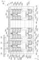
次に、本実施形態におけるバーンインボード20について、図3及び図4を参照しながら説明する。図3は本実施形態におけるバーンインボードの配線系統を示す平面模式図であり、図4は図3のIV部の拡大図である。Next, the burn-in
本実施形態におけるバーンインボード20は、図3に示すように、配線板30と、当該配線板30に実装された複数(本例では320個)のソケット70A1~70P20と、当該配線板30に実装されたコネクタ80と、を備えている。 As shown in FIG. 3 , the burn-in
ソケット70A1~70P20には、DUT100をそれぞれ装着することが可能となっている。以下において、ソケット70A1~70P20を総称してソケット70とも称する。また、コネクタ80は、配線板30の基板40において一方の端部(図3において上側の縁部)41に実装されており、上述のように、バーンインチャンバ11に設けられたコネクタ115に嵌合することが可能となっている。なお、このバーンインボード20が、配線板30を補強する補強枠や、当該配線板の裏面を保護するボトムカバーを備えていてもよい。
なお、本実施形態におけるソケット70A1が本発明における「第1のソケット」の一例に相当し、本実施形態におけるソケット70A2が本発明における「第2のソケット」の一例に相当し、本実施形態におけるソケット70B1が本発明における「第3のソケット」の一例に相当し、本実施形態におけるソケット70B2が本発明における「第4のソケット」の一例に相当する。また、本実施形態におけるソケット70A1が本発明における「第5のソケット」の一例に相当し、ソケット70A2が本発明における「第6のソケット」の一例に相当し、ソケット70A3が本発明における「第7のソケット」の一例に相当する。 The socket70A1 in this embodiment corresponds to an example of the "first socket" in the present invention, the socket70A2 in this embodiment corresponds to an example of the "second socket" in the present invention, the socket70B1 in this embodiment corresponds to an example of the "third socket" in the present invention, and the socket70B2 in this embodiment corresponds to an example of the "fourth socket" in the present invention. Also, the socket70A1 in this embodiment corresponds to an example of the "fifth socket" in the present invention, the socket70A2 corresponds to an example of the "sixth socket" in the present invention, and the socket70A3 corresponds to an example of the "seventh socket" in the present invention.
それぞれのソケット70は、図4に示すように、DUT100の端子に接触する複数(本例では16本)のコンタクトピン71を有している。この複数のコンタクトピン71は、DUT100の端子に対応するようにマトリクス状に配置されている。バーンイン試験に際して、DUT100がソケット70に装着されると、このコンタクトピン71がDUT100の端子に接触することで、DUT100とソケット70とが電気的に接続される。ソケット70A1~70P20は、いずれも同一の構造を有している。 4, each
なお、ソケット70が有するコンタクトピン71の本数は、特に上記に限定されない。また、ソケット70が有するコンタクトピン71の配置も、特に上記に限定されない。The number of contact pins 71 in the
そして、図3に示すように、複数のソケット70A1~70P20は、配線板30の基板40上にマトリクス状に配置されている。 As shown in FIG. 3, the plurality of sockets 70A1 to 70P20 are arranged in a matrix on the
より具体的には、本実施形態では、基板40において第1の方向に沿って20個のソケット70A1~70A20が一例に並べられており、これらのソケット70A1~70A20によって一つのソケット列75Aが構成されている。なお、この第1の方向は、基板40において、第1の端部41から、当該第1の端部41とは反対側の第2の端部42に向かう方向であり、図中の-Y方向に相当する。このソケット列75Aを構成する20個のソケット70A1~70A20は、実質的に等間隔に並べられている。 More specifically, in this embodiment, twenty sockets 70A1 to 70A20 are arranged in a first direction on the
同様に、第1の方向に沿って並ぶ20個のソケット70B1~70B20が一列に並べられており、これらのソケット70B1~70B20によって一つのソケット列75Bが構成されている。このソケット列75Bを構成する20個のソケット70B1~70B20も、実質的に等間隔に並べられている。同じ要領で、他の14個のソケット列75C~75Pも、第1の方向に沿って等間隔で並べられた20個のソケット70によってそれぞれ構成されている。 Similarly, 20 sockets 70B1 to 70B20 are aligned in a row along the first direction, and these sockets 70B1 to 70B20 constitute one
そして、これらの合計16個のソケット列75A~75Pは、第2の方向に沿って並べられている。なお、この第2の方向は、上述した第1の方向(図中の-Y方向)に対して実質的に直交する方向であり、図中のX方向に相当する。このソケット列75A~75Pは、実質的に等間隔に並べられている。These 16
なお、基板40上に実装されるソケット70の数は、特に上記に限定されない。また、基板40上におけるソケット70の配置も、特に上記に限定されない。 The number of
本実施形態における配線板30は、上述した複数のソケット70A1~70P20が実装されたプリント配線板である。この配線板30は、図3に示すように、電気絶縁性を有する基板40と、2種類の配線系統50a1~50h10,60a~60pと、を備えている。本実施形態では、配線板30は多層の配線板であり、それぞれの配線系統50a1~50h10,60a~60pは、基板40に形成された配線パターン及びビアホール等の導電路によって構成されている。 The
本実施形態では、第1の配線系統50a1~50h10の接続形態の種類と、第2の配線系統60a~60pの接続形態の種類とが相違している。ここで、接続形態(Connection form/Connection topology)とは、配線板30におけるコネクタ80と複数のソケット70との間の電気的な接続の形態であり、コネクタ80と複数のソケット70とを接続する配線及び分岐点を組み合わせて構成される接続経路(配線及び分岐点の位置関係)によって表現される。そして、この接続形態の種類は、分岐点の有無や当該分岐点の位置によって分類することができる。本実施形態では、第1の配線系統50a1~50h10は、分岐点を有する接続形態を有しているのに対し、第2の配線系統60a~60pは、分岐点を有しない接続形態を有している。なお、配線板30が有する配線系統の接続形態の種類の数は特に限定されず、配線板が3種類以上の接続形態の配線系統を備えていてもよい。 In this embodiment, the type of connection form of the first wiring system 50a1 to 50h10 is different from the type of connection form of the
第1の配線系統50a1~50h10は、基本的に同一の構成を有しているので、以下に第1の配線系統50a1の構成について代表的に説明し、他の第1の配線系統50a2~50h10の構成の説明については省略する。同様に、第2の配線系統60a~60pは、基本的に同一の構成を有しているので、以下に第2の配線系統60aの構成について代表的に説明し、他の第2の配線系統60b~60pの構成の説明については省略する。 Since the first wiring systems50a1 to50h10 basically have the same configuration, the configuration of the first wiring system50a1 will be described below as a representative, and descriptions of the configurations of the other first wiring systems50a2 to50h10 will be omitted. Similarly, the
第1の配線系統50a1は、コネクタ80とソケット70A1との間で配線が分岐してソケット70B1に接続された部分を有する接続形態を有している。具体的には、この第1の配線系統50a1は、図4に示すように、主線51と、副線52,53と、接続線54,55と、を備えている。なお、この主線51、副線52,53、及び、接続線54,55は、基板40に形成された配線パターン及びビアホール等の導電路によって構成されている。 The first wiring system50a1 has a connection form in which wiring branches between the
なお、本実施形態における主線51が本発明における「第1の主線」の一例に相当し、本実施形態における副線52が本発明における「第1の副線」の一例に相当し、本実施形態における副線53が本発明における「第2の副線」の一例に相当し、本実施形態における接続線54が本発明における「第1の接続線」の一例に相当し、本実施形態における接続線55が本発明における「第2の接続線」の一例に相当する。The
主線51は、その一端でコネクタ80に接続されている。この主線51の他端には分岐点511が設けられており、この分岐点511で主線51は2つの副線52,53に分岐している。一方の副線52は、その先端で、接続線54に接続されていると共にソケット70A1にも接続されている。そして、この接続線54は、その先端で次のソケット70A2に接続されている。同様に、他方の副線53も、その先端で、接続線55に接続されていると共にソケット70B1にも接続されている。そして、この接続線55は、その先端で次のソケット70B2に接続されている。 One end of the
すなわち、この第1の配線系統50a1では、コネクタ80とソケット70A1,70B1との間で配線が2つに分岐している。そして、この第1の配線系統50a1では、一方の副線52に接続されたソケット70A1と、第1の方向に沿って当該ソケット70A1に並んでいるソケット70A2とが、接続線54によってデイジーチェーン状に接続されている。同様に、この第1の配線系統50a1では、他方の副線53に接続されたソケット70B1と、第1の方向に沿って当該ソケット70B1に並んでいるソケット70B2とが、接続線55によってデイジーチェーン状に接続されている。 That is, in the first wiring system50a1, the wiring is branched into two between the connector 80 and the sockets 70A1 and 70B1. In the first wiring system 50a1,thesocket 70A1 connected to one of the secondary lines52 and the socket70A2 adjacent to the socket70A1 in the first direction are connected in a daisy chain by a
本実施形態では、分岐点511とソケット70A1との間の副線52の長さと、分岐点511とソケット70B1との間の副線53の長さとが実質的に同一となっている。このため、ソケット70A1の信号の伝送時間と、ソケット70B1の信号の伝送時間とが実質的に同一となっている。 In this embodiment, the length of the
また、ソケット70A1とソケット70A2の間の接続線54の長さと、ソケット70B1とソケット70B2との間の接続線55の長さとが実質的に同一となっている。従って、分岐点511とソケット70A2との間の副線52及び接続線54の合計の長さと、分岐点511とソケット70B2との間の副線53及び接続線55の合計の長さとが実質的に同一となっている。このため、ソケット70A2の信号の伝送時間と、ソケット70B2の信号の伝送時間とが実質的に同一となっている。 Furthermore, the length of the
第1の配線系統50a2も、上述した第1の配線系統50a1と同様の配線系統を有しており、図3に示すように、コネクタ80と4つのソケット70A3,70A4,70B3,70B4とを接続している。 The first wiring system50a2 also has a wiring system similar to the above-mentioned first wiring system50a1 , and as shown in FIG. 3, connects the
特に図示しないが、第1の配線系統50a3~50a9も上述した第1の配線系統50a1と同様の配線系統を有しており、第1の配線系統50a3がコネクタ80と4つのソケット70A5,70A6,70B5,70B6とを接続し、第1の配線系統50a4がコネクタ80と4つのソケット70A7,70A8,70B7,70B8とを接続し、第1の配線系統50a5がコネクタ80と4つのソケット70A9,70A10,70B9,70B10とを接続し、第1の配線系統50a6がコネクタ80と4つのソケット70A11,70A12,70B11,70B12とを接続し、第1の配線系統50a7がコネクタ80と4つのソケット70A13,70A14,70B13,70B14とを接続し、第1の配線系統50a8がコネクタ80と4つのソケット70A15,70A16,70B15,70B16とを接続し、第1の配線系統50a9がコネクタ80と4つのソケット70A17,70A18,70B17,70B18とを接続している。 Although not specifically shown, the first wiring systems50a3 to50a9 also have wiring systems similar to the above-mentioned first wiring system50a1 , with the first wiring system50a3 connecting the
第1の配線系統50a10も、上述した第1の配線系統50a1と同様の配線系統を有しており、図3に示すように、コネクタ80と4つのソケット70A19,70A20,70B19,70B20とを接続している。 The first wiring system50a10 also has a wiring system similar to the above-mentioned first wiring system50a1 , and as shown in FIG. 3, connects a
すなわち、2つのソケット列75A,75Bに対して、ソケット70を4個ずつコネクタ80に接続する第1の接続形態50a1~50a10が10個設けられている。同様に、他のソケット列75C~75Pにおいて、2つのソケット列毎に10個の第1の接続形態50b1~50h10が設けられている。結果的に、本実施形態のバーンインボード20は、320個のソケット70A1~70P20に対して、80個の第1の接続形態50a1~50h10を備えている。 That is, ten first connection configurations50a1-50a10 are provided for two socket rows 75A, 75B, each connecting four sockets 70 to the connector 80. Similarly, ten first connection configurations 50b1-50h10areprovidedfor each of the other socket rows75C -75P . As a result, the burn-in
これに対し、第2の配線系統60aは、コネクタ80とソケット70A1~70A20との間で配線が分岐する部分を有していない接続形態を有している。具体的には、この第2の配線系統60aは、図3及び図4に示すように、主線61aと、接続線62a1~62a19と、を備えている。なお、この主線61a、及び、接続線62a1~62a19は、基板40に形成された配線パターン及びビアホール等の導電路によって構成されている。 In contrast, the
なお、本実施形態における主線61aが本発明における「第2の主線」の一例に相当し、本実施形態における接続線62a1が本発明における「第3の接続線」の一例に相当し、本実施形態における接続線62a2が本発明における「第4の接続線」の一例に相当する。 The
主線61aは、その一端でコネクタ80に接続されている。この主線61aの他端は、接続線62a1に接続されていると共に、ソケット70A1に接続されている。そして、この接続線62a1は、その先端で、次の接続線62a2に接続されていると共に次のソケット70A2にも接続されている。同様に、接続線62a2~62a18が、その先端で、次の接続線62a3~62a19に接続されていると共に次のソケット70A3~70A19にも接続されている。そして、最後の接続線62a19が、その先端でソケット70A20に接続されている。 One end of the
すなわち、この第2の配線系統60aでは、コネクタ80とソケット70A1~70A20との間で配線が一切分岐していない。この第2の配線系統60aでは、第1の方向に沿って一列に並んでソケット列75Aを構成している20個のソケット70A1~70A20が、接続線62a1~62a19によってデイジーチェーン状に接続されている。 That is, in this
第2の配線系統60bも、上述した第2の配線系統60aと同様の配線系統を有しており、ソケット列75Bを構成する20個のソケット70B1~70B20をデイジーチェーン状に接続している。すなわち、図3及び図4に示すように、主線61bと、接続線62b1~62b19と、を備えている。主線61bは、その一端でコネクタ80に接続されている。この主線61bの他端は、接続線62b1に接続されていると共に、ソケット70B1にも接続されている。そして、20個のソケット70B1~70B20が接続線62b1~62b19によってデイジーチェーン状に接続されている。 The
同様に、第2の配線系統60c~60pも上述した第2の配線系統60aと同様の配線系統を有しており、それぞれの第2の配線系統60c~60pが、ソケット列75C~75Pをそれぞれ構成する20個のソケット70をデイジーチェーン状に接続している。Similarly, the
すなわち、一つのソケット列75A~75Pに対して、一つの第2の配線系統60a~60pが設けられており、結果的に、本実施形態のバーンインボード20は、320個のソケット70A1~70P20に対して、16個の第2の配線系統60a~60pを備えている。 That is, one
それぞれの第1の配線系統50a1~50h10は、コネクタ80に独立して個別に接続されている。そして、それぞれの第1の配線系統50a1~50h10は、当該コネクタ80を介して、バーンインコントローラ13が有する別々のドライバに接続されている。一例を挙げれば、図3に示すように、第1の配線系統50a1はドライバ14bに接続されているのに対し、別の第1の配線系統50a2は当該ドライバ14bとは別のドライバ14cに接続されている。 Each of the first wiring systems 50a1 to 50h10 is connected independently and individually to a
また、第1の配線系統50a1は、図4に示すように、ソケット70A1,70A2,70B1,70B2が有するコンタクトピン71の中で同一のコンタクトピン71a(例えば、図中において3行3列に位置するコンタクトピン71a)に接続されている。同様に、他の第1の配線系統50a2~50h10もソケット70において同じコンタクトピン71aに接続されている。 4, the first wiring system 50a-1is connected to the
そして、この第1の配線系統50a1~50h10を介してバーンインコントローラ13とソケット70との間で伝送される第1の信号は、当該ソケット70に電気的に接続されるDUT100に入力される入力信号と、当該DUT100から出力される出力信号との両方を含んでいる。こうした第1の信号の具体的としては、DUT100へのデータの書き込みを行う信号と、当該DUT100からデータの読み出しを行う信号と、を含む信号を例示することができる。この第1の信号は高い品質の波形が要求される信号であり、一つの配線系統に接続されているソケットの数が少ないほど信号の波形品質が良くなるため、本実施形態では、それぞれの第1の配線系統50a1~50h10は、4個のソケット70のみに接続されている。 The first signal transmitted between the burn-in
なお、第1の配線系統が有する分岐点の数は一つに限定されず、例えば、第1の配線系統が複数の分岐点を有していてもよい。因みに、信号の周波数が高いほど波形品質に影響を与えるため、分岐部の数は少ない方が好ましい。The number of branch points in the first wiring system is not limited to one, and for example, the first wiring system may have multiple branch points. Incidentally, the higher the signal frequency, the more it affects the waveform quality, so it is preferable to have a smaller number of branch points.
それぞれの第2の配線系統60a~60pも、コネクタ80に独立して個別に接続されている。そして、それぞれの第2の配線系統60a~60pは、当該コネクタ80を介してバーンインコントローラ13が有する別々のドライバに接続されている。一例を挙げれば、図3に示すように、第2の配線系統60aはドライバ14aに接続されているのに対し、別の第2の配線系統60bは当該ドライバ14aとは別のドライバ14dに接続されている。なお、ドライバ14a,14dは、上述の第1の配線系統50a1,50a2が接続されたドライバ14b,14cとも異なるドライバである。 Each of the
また、第2の配線系統60aは、図4に示すように、ソケット70A1~70A20が有するコンタクトピン71の中で、上述の第1の配線系統50aが接続されるコンタクトピン71aとは別のコンタクトピン71b(例えば、図中において2行2列に位置するコンタクトピン71b)に接続されている。同様に、他の第2の配線系統60b~60pもソケット70において同じコンタクトピン71bに接続されている。 4, the
そして、この第2の配線系統60aを介してバーンインコントローラ13とソケット70との間で伝送される第2の信号は、当該ソケット70に電気的に接続されるDUT100に入力される入力信号のみを含んでいる。こうした第2の信号の具体例としては、例えば、アドレス信号やクロック信号等を例示することができる。この第2の信号は、上記の第1の信号と比較して高い品質の波形が要求されないため、本実施形態では、それぞれの第2の配線系統60a~60pは、20個のソケット70に接続されている。The second signal transmitted between the burn-in
なお、一つの第2の配線系統によって接続するソケット70の数は、特に上記に限定されず、要求される波形品質等に応じて設定することができる。例えば、一つの第2の配線系統によって、5個のソケット70をデイジーチェーン状に接続してもよい。或いは、一つの第2の配線系統によって、10個のソケット70をデイジーチェーン状に接続してもよい。The number of
特に図示しないが、ソケット70が有する上記のコンタクトピン71a,71b以外のコンタクトピン71にも、他の配線系統が接続されている。すなわち、ソケット70が有する全てのコンタクトピン71に配線系統がそれぞれ独立して接続されている。 Although not particularly shown, other wiring systems are connected to the contact pins71 other than the contact pins 71a and 71b of the
当該他の配線系統が、上述した第1或いは第2の配線系統と同じ種類の接続形態を有していてもよいし、第1及び第2の配線形態とは異なる種類の接続形態を有していてもよい。例えば、当該他の配線系統が、上述した第1の配線形態とは異なる位置に分岐点を有する接続形態を有していてもよい。これらの他の配線系統の接続形態は、要求される波形品質等に応じて設定することができる。The other wiring system may have the same type of connection as the first or second wiring system described above, or may have a different type of connection from the first and second wiring systems. For example, the other wiring system may have a connection that has a branch point at a position different from the first wiring system described above. The connection forms of these other wiring systems can be set according to the required waveform quality, etc.
ここで、入力信号については、バーンインコントローラ13がタイミング補正機能を備えている場合には、このタイミング補正機能のキャリブレーションにより、全てのDUT100に対して同じタイミングで信号が入力することができる。これに対し、DUT100からの出力信号については、このタイミング補正機能を用いてもタイミングを合わせることが困難である。そのため、コネクタとソケットとの間の配線の長さに応じて、信号の伝送遅延時間が生じてしまう。なお、こうした伝送遅延時間に起因する問題は、信号の周波数が高くなるほど顕著になる傾向がある。Regarding input signals, if the burn-in
このため、本実施形態では、出力信号を含む第1の信号を伝送する第1の配線系統50a1~50h10の接続形態を、上述のような分岐点511を有する第1の接続形態とする。これにより、バーンインボード20上のソケット70の数が増加した場合であっても、第1の信号の伝送遅延時間を低減することができる。 For this reason, in this embodiment, the connection form of the first wiring system 50a1 to 50h10 that transmits the first signal including the output signal is the above-mentioned first connection form having the
一例を挙げれば、ソケット70の数の増加に伴って4つのソケット70A1~70A4を一列にデイジーチェーン状に接続する場合と比較して、ソケット70A3,70A4をコネクタ80に近いソケット70B1,70B2に替えて、4つのソケット70A1,70A2,70B1,70B2を上述の第1の配線系統50a1で接続することで、コネクタ80からソケット70B1、70B2までの配線の長さを短くすることができる。 As an example, compared to connecting four sockets70A1 to70A4 in a row in a daisy chain as the number of
一方で、第2の信号は第1の信号と比較して高い品質の波形が要求されないので、当該第2の信号を伝送する第2の配線系統60a~60pの接続形態を、上述のような分岐点を有しない第2の接続形態とする。これにより、デイジーチェーン状に接続するソケット70の数を増加させることで、ドライバの数が限られている中でソケット70の数の増加に対処することができる。On the other hand, since the second signal does not require a waveform of high quality compared to the first signal, the connection form of the
従って、本実施形態では、信号の種類に応じて配線系統の接続形態の種類を異ならせることで、ソケット70の数が増加した場合であっても、バーンイン試験の品質の低下の抑制を図ることができる。Therefore, in this embodiment, by varying the type of wiring system connection depending on the type of signal, it is possible to suppress deterioration in the quality of the burn-in test even if the number of
なお、以上説明した実施形態は、本発明の理解を容易にするために記載されたものであって、本発明を限定するために記載されたものではない。したがって、上記の実施形態に開示された各要素は、本発明の技術的範囲に属する全ての設計変更や均等物をも含む趣旨である。The above-described embodiments are described to facilitate understanding of the present invention, and are not described to limit the present invention. Therefore, each element disclosed in the above embodiments is intended to include all design modifications and equivalents that fall within the technical scope of the present invention.
例えば、上述したバーンイン装置1の構成は、一例に過ぎず、特に上記に限定されない。例えば、上述のバーンイン装置1は、恒温室111を用いてDUT100の温度調整を行う方式であるが、特にこれに限定されない。例えば、バーンイン装置1が、DUT100に温度調整用のプッシャを接触させることで当該DUTの温度調整を行う方式であってもよい。For example, the configuration of the burn-in
1…バーンイン装置
11…バーンインチャンバ
111…恒温室
112…ドア
113…スロット
114…レール
115…コネクタ
116…エバポレータ
117…ヒータ
118…ファン
12…試験用電源
13…バーンインコントローラ
14a~14d…ドライバ
20…バーンインボード
30…配線板
40…基板
41…端部
42…端部
50a1~50h10…第1の配線系統
51…主線
511…分岐点
52,53…副線
54,55…接続線
60a~60p…第2の配線系統
61a,61b…主線
62a1~62a19,62b1~62b19…接続線
70,70A1~70P20…ソケット
71,71a,71b…コンタクトピン
75A~75P…ソケット列
80…コネクタ
100…DUTREFERENCE SIGNS
511:
Claims (8)
Translated fromJapanese前記基板に実装された複数のソケットと、
前記基板に実装されたコネクタと、
前記基板に設けられ、前記複数のソケットと前記コネクタとを接続する複数の配線系統と、を備えており、
前記複数の配線系統は、
第1の信号を伝送する第1の配線系統と、
前記第1の信号とは異なる第2の信号を伝送する第2の配線系統と、を含み、
前記第1の配線系統の第1の接続形態は、前記コネクタと前記ソケットとの間で配線が分岐して他の前記ソケットに接続された部分を有する接続形態であり、
前記第2の配線系統の第2の接続形態は、前記コネクタと前記ソケットとの間で配線が分岐する部分を有していない接続形態であり、
前記第1の配線系統に接続されている前記ソケットの数は、前記第2の配線系統に接続されている前記ソケットの数よりも少ないバーンインボード。A substrate;
A plurality of sockets mounted on the substrate;
A connector mounted on the substrate;
a plurality of wiring systems provided on the board and connecting the plurality of sockets and the connector;
The plurality of wiring systems include
a first wiring system for transmitting a first signal;
a second wiring system transmitting a second signal different from the first signal;
a first connection formof the first wiring system is a connection form in which a wiring is branched between the connector and the socket and has a portion connected to another ofthe sockets ,
a second connection formof the second wiring systemis a connection form in which no wiring branch is provided between the connector and the socket,
A burn-in boardin which the number of the sockets connected to the first wiring system is smaller than the number of the sockets connected to the second wiring system .
前記ソケットは、第1~第4のソケットを含んでおり、
前記第1の配線系統は、
前記コネクタに接続された第1の主線と、
前記第1の主線に分岐点で接続されていると共に、前記第1及び前記第3のソケットにそれぞれ接続された第1及び第2の副線と、
前記第1のソケットと前記第2のソケットとを接続する第1の接続線と、
前記第3のソケットと前記第4のソケットとを接続する第2の接続線と、を含むバーンインボード。 2. The burn-in board of claim 1,
The sockets include first to fourth sockets,
The first wiring system includes:
a first main line connected to the connector;
first and second sub-lines connected to the first main line at a branch point and connected to the first and third sockets, respectively;
a first connection line connecting the first socket and the second socket;
a second connecting line connecting the third socket and the fourth socket.
前記基板は、
前記コネクタが実装された第1の端部と、
前記第1の端部とは反対側の第2の端部と、を有し、
前記第1及び第2のソケットは、前記第1の端部から前記第2の端部に向かう第1の方向に沿って並び、
前記第3及び第4のソケットは、前記第1の方向に沿って並び、
前記第1及び第3のソケットは、前記第1の方向に対して直交する第2の方向に沿って並び、
前記第2及び第4のソケットは、前記第2の方向に沿って並んでいるバーンインボード。 3. The burn-in board of claim2 ,
The substrate is
a first end having the connector mounted thereon;
a second end opposite the first end,
the first and second sockets are aligned along a first direction from the first end to the second end;
the third and fourth sockets are aligned along the first direction,
the first and third sockets are aligned along a second directionperpendicular to the first direction;
The second and fourth sockets are aligned along the second direction on the burn-in board.
前記分岐点と前記第1のソケットとの間の配線の長さと、前記分岐点と前記第3のソケットとの間の配線の長さとが同一であり、
前記分岐点と前記第2のソケットとの間の配線の長さと、前記分岐点と前記第4のソケットとの間の配線の長さとが同一であるバーンインボード。4. The burn-in board according to claim2 ,
a length of a wiring between the branch point and the first socket isequal to a length of a wiring between the branch point and the third socket;
a burn-in board in which the length of the wiring between the branch point and the second socketis the same as the length of the wiring between the branch point and the fourth socket;
前記ソケットは、第5~第7のソケットを含んでおり、
前記第2の配線系統は、
前記コネクタに接続されていると共に、前記第5のソケットに接続された第2の主線と、
前記第5のソケットと前記第6のソケットとを接続する第3の接続線と、
前記第6のソケットと前記第7のソケットとを接続する第4の接続線と、を含み、
前記第1のソケットと前記第5のソケットは、同一のソケットであり、
前記第2のソケットと前記第6のソケットは、同一のソケットであるバーンインボード。 The burn-in board according to any one of claims2 to 4 ,
The sockets include fifth to seventh sockets,
The second wiring system includes:
a second main line connected to the connector and to the fifth socket;
a third connection line connecting the fifth socket and the sixth socket;
a fourth connection line connecting the sixth socket and the seventh socket;
the first socket and the fifth socket are the same socket,
The second socket and the sixth socket are the same socket on the burn-in board.
前記基板は、
前記コネクタが実装された第1の端部と、
前記第1の端部とは反対側の第2の端部と、を有しており、
前記第5~第7のソケットは、前記第1の端部から前記第2の端部に向かう第1の方向に沿って順に並べられているバーンインボード。 6. The burn-in board of claim5 ,
The substrate is
a first end having the connector mounted thereon;
a second end opposite the first end,
The fifth to seventh sockets are arranged in order along a first direction from the first end to the second end of the burn-in board.
前記第1の信号は、前記ソケットに電気的に接続されるDUTからの出力信号を含み、
前記第2の信号は、前記DUTへの入力信号を含むバーンインボード。 The burn-in board according to any one of claims 1 to6 ,
the first signal includes an output signal from a DUT electrically connected to the socket;
The second signal includes an input signal to the DUT.
Priority Applications (5)
| Application Number | Priority Date | Filing Date | Title |
|---|---|---|---|
| JP2021070504AJP7623204B2 (en) | 2021-04-19 | 2021-04-19 | Burn-in board and burn-in device |
| KR1020220028508AKR102789995B1 (en) | 2021-04-19 | 2022-03-07 | Burn-in board and burn-in device |
| CN202210223654.5ACN115219876A (en) | 2021-04-19 | 2022-03-09 | Burning board and burning device |
| TW111110309ATWI808687B (en) | 2021-04-19 | 2022-03-21 | Burn-in plate, and burn-in device |
| US17/703,992US11719741B2 (en) | 2021-04-19 | 2022-03-25 | Burn-in board and burn-in apparatus |
Applications Claiming Priority (1)
| Application Number | Priority Date | Filing Date | Title |
|---|---|---|---|
| JP2021070504AJP7623204B2 (en) | 2021-04-19 | 2021-04-19 | Burn-in board and burn-in device |
Publications (2)
| Publication Number | Publication Date |
|---|---|
| JP2022165234A JP2022165234A (en) | 2022-10-31 |
| JP7623204B2true JP7623204B2 (en) | 2025-01-28 |
Family
ID=83602452
Family Applications (1)
| Application Number | Title | Priority Date | Filing Date |
|---|---|---|---|
| JP2021070504AActiveJP7623204B2 (en) | 2021-04-19 | 2021-04-19 | Burn-in board and burn-in device |
Country Status (5)
| Country | Link |
|---|---|
| US (1) | US11719741B2 (en) |
| JP (1) | JP7623204B2 (en) |
| KR (1) | KR102789995B1 (en) |
| CN (1) | CN115219876A (en) |
| TW (1) | TWI808687B (en) |
Families Citing this family (3)
| Publication number | Priority date | Publication date | Assignee | Title |
|---|---|---|---|---|
| JP7623204B2 (en)* | 2021-04-19 | 2025-01-28 | 株式会社アドバンテスト | Burn-in board and burn-in device |
| KR102557146B1 (en) | 2022-12-29 | 2023-07-19 | 주식회사 유수 | Test board for burn-in test of semiconductor chip |
| CN117292737A (en)* | 2023-10-11 | 2023-12-26 | 合肥兆芯电子有限公司 | Temperature change test system and operation method thereof |
Citations (8)
| Publication number | Priority date | Publication date | Assignee | Title |
|---|---|---|---|---|
| JP2001349925A (en) | 2000-06-09 | 2001-12-21 | Mitsubishi Electric Corp | Inspection apparatus and inspection method for semiconductor integrated circuit |
| JP2004205391A (en) | 2002-12-26 | 2004-07-22 | Renesas Technology Corp | Semiconductor testing device |
| US6815966B1 (en) | 2002-06-27 | 2004-11-09 | Aehr Test Systems | System for burn-in testing of electronic devices |
| US6982566B1 (en) | 2004-04-01 | 2006-01-03 | Altera Corporation | Method and apparatus for operating a burn-in board to achieve lower equilibrium temperature and to minimize thermal runaway |
| WO2008093807A1 (en) | 2007-02-01 | 2008-08-07 | Fujitsu Limited | Monitor burn-in test device and monitor burn-in test method |
| JP2012207958A (en) | 2011-03-29 | 2012-10-25 | Renesas Electronics Corp | Manufacturing method of semiconductor device |
| US20150084051A1 (en) | 2013-09-26 | 2015-03-26 | Renesas Electronics Corporation | Electronic Device, Test Board, and Semiconductor Device Manufacturing Method |
| JP2016125886A (en) | 2014-12-26 | 2016-07-11 | ルネサスエレクトロニクス株式会社 | Manufacturing method of semiconductor device |
Family Cites Families (21)
| Publication number | Priority date | Publication date | Assignee | Title |
|---|---|---|---|---|
| JPH09229995A (en)* | 1996-02-20 | 1997-09-05 | Fujitsu Ltd | Burn-in test board and burn-in test method using the same |
| JPH1183938A (en)* | 1997-09-08 | 1999-03-26 | Mitsubishi Electric Corp | Semiconductor device test board and semiconductor device evaluation test method using the same |
| US5794175A (en)* | 1997-09-09 | 1998-08-11 | Teradyne, Inc. | Low cost, highly parallel memory tester |
| US20020070745A1 (en)* | 2000-04-27 | 2002-06-13 | Johnson James E. | Cooling system for burn-in unit |
| US6472895B2 (en)* | 2000-12-06 | 2002-10-29 | Advanced Micro Devices, Inc. | Method and system for adapting burn-in boards to multiple burn-in systems |
| US7345495B2 (en)* | 2004-06-30 | 2008-03-18 | Intel Corporation | Temperature and voltage controlled integrated circuit processes |
| CN100501707C (en)* | 2006-08-15 | 2009-06-17 | 中兴通讯股份有限公司 | Device and method for realizing on-board programming of boot code chip of processor system |
| JP2009204329A (en)* | 2008-02-26 | 2009-09-10 | Nec Electronics Corp | Circuit board inspecting system and inspection method |
| CN201311636Y (en)* | 2008-12-19 | 2009-09-16 | 深圳市神舟电脑有限公司 | Display device burning system |
| JP2011242197A (en)* | 2010-05-17 | 2011-12-01 | Nippon Eng Kk | Burn-in board, burn-in apparatus, and burn-in system |
| JP2014025829A (en) | 2012-07-27 | 2014-02-06 | Advantest Corp | Burn-in board and burn-in device |
| KR20160007138A (en)* | 2014-07-11 | 2016-01-20 | (주)인포큐브 | Burn in test module |
| KR101857124B1 (en)* | 2016-10-25 | 2018-06-21 | (주)유니테스트 | Test board for burn-in testing |
| US10101382B2 (en)* | 2016-12-30 | 2018-10-16 | Texas Instruments Incorporated | Systems and methods for dynamic Rdson measurement |
| CN111051902B (en) | 2017-07-25 | 2022-05-27 | 皇虎科技(加拿大)有限公司 | System and method for automatic burn-in testing on integrated circuit devices |
| CN207458044U (en)* | 2017-11-29 | 2018-06-05 | 郑州云海信息技术有限公司 | A kind of multi-functional Transfer plates |
| CN108063838B (en)* | 2017-12-26 | 2021-03-09 | 广州视源电子科技股份有限公司 | Method and device for automatically burning MAC address on board card and board card |
| CN207946804U (en)* | 2018-03-14 | 2018-10-09 | 达特电子(上海)有限公司 | A kind of burning adapter and programming system |
| JP7143134B2 (en)* | 2018-07-26 | 2022-09-28 | 株式会社アドバンテスト | Load board and electronic component test equipment |
| JP7198127B2 (en)* | 2019-03-20 | 2022-12-28 | 株式会社アドバンテスト | Interposers, sockets, socket assemblies and wiring board assemblies |
| JP7623204B2 (en)* | 2021-04-19 | 2025-01-28 | 株式会社アドバンテスト | Burn-in board and burn-in device |
- 2021
- 2021-04-19JPJP2021070504Apatent/JP7623204B2/enactiveActive
- 2022
- 2022-03-07KRKR1020220028508Apatent/KR102789995B1/enactiveActive
- 2022-03-09CNCN202210223654.5Apatent/CN115219876A/enactivePending
- 2022-03-21TWTW111110309Apatent/TWI808687B/enactive
- 2022-03-25USUS17/703,992patent/US11719741B2/enactiveActive
Patent Citations (9)
| Publication number | Priority date | Publication date | Assignee | Title |
|---|---|---|---|---|
| JP2001349925A (en) | 2000-06-09 | 2001-12-21 | Mitsubishi Electric Corp | Inspection apparatus and inspection method for semiconductor integrated circuit |
| US6815966B1 (en) | 2002-06-27 | 2004-11-09 | Aehr Test Systems | System for burn-in testing of electronic devices |
| JP2004205391A (en) | 2002-12-26 | 2004-07-22 | Renesas Technology Corp | Semiconductor testing device |
| US6982566B1 (en) | 2004-04-01 | 2006-01-03 | Altera Corporation | Method and apparatus for operating a burn-in board to achieve lower equilibrium temperature and to minimize thermal runaway |
| WO2008093807A1 (en) | 2007-02-01 | 2008-08-07 | Fujitsu Limited | Monitor burn-in test device and monitor burn-in test method |
| US20090287362A1 (en) | 2007-02-01 | 2009-11-19 | Fujitsu Limited | Monitored burn-in test apparatus and monitored burn-in test method |
| JP2012207958A (en) | 2011-03-29 | 2012-10-25 | Renesas Electronics Corp | Manufacturing method of semiconductor device |
| US20150084051A1 (en) | 2013-09-26 | 2015-03-26 | Renesas Electronics Corporation | Electronic Device, Test Board, and Semiconductor Device Manufacturing Method |
| JP2016125886A (en) | 2014-12-26 | 2016-07-11 | ルネサスエレクトロニクス株式会社 | Manufacturing method of semiconductor device |
Also Published As
| Publication number | Publication date |
|---|---|
| US20220334173A1 (en) | 2022-10-20 |
| KR20220144306A (en) | 2022-10-26 |
| TWI808687B (en) | 2023-07-11 |
| KR102789995B1 (en) | 2025-04-01 |
| US11719741B2 (en) | 2023-08-08 |
| CN115219876A (en) | 2022-10-21 |
| TW202244516A (en) | 2022-11-16 |
| JP2022165234A (en) | 2022-10-31 |
Similar Documents
| Publication | Publication Date | Title |
|---|---|---|
| JP7623204B2 (en) | Burn-in board and burn-in device | |
| US6562636B1 (en) | Wafer level burn-in and electrical test system and method | |
| KR100371953B1 (en) | Low cost, highly parallel memory tester | |
| KR20020038597A (en) | Semiconductor parallel tester | |
| TW201329470A (en) | Test system and test method for PCBA | |
| KR20020075733A (en) | Method and apparatus for socket calibration of integrated circuit testers | |
| JP5024861B2 (en) | Probe card | |
| KR20010096955A (en) | Board for testing semiconductor device and testing apparatus for semiconductor device comprising the same | |
| KR20020036835A (en) | Wafer level burn-in and electrical test system and method | |
| US6181146B1 (en) | Burn-in board | |
| JP3864201B2 (en) | Probe card | |
| JP7623203B2 (en) | Burn-in board and burn-in device | |
| KR100761894B1 (en) | Semiconductor device testing apparatus and device interface board | |
| TWI861937B (en) | Automatic testing device and its interface device | |
| TWI870900B (en) | Automatic testing device and its interface device | |
| JP2624144B2 (en) | Test board | |
| TWI876380B (en) | Automatic testing device and its interface device | |
| TWI872573B (en) | Automatic testing device and its interface device | |
| US20250277845A1 (en) | Test board for burn-in test | |
| JPS62257072A (en) | Burn-in device | |
| US20090315584A1 (en) | Measuring board for examining different types of sections of mcp product |
Legal Events
| Date | Code | Title | Description |
|---|---|---|---|
| A621 | Written request for application examination | Free format text:JAPANESE INTERMEDIATE CODE: A621 Effective date:20240209 | |
| A977 | Report on retrieval | Free format text:JAPANESE INTERMEDIATE CODE: A971007 Effective date:20240930 | |
| A131 | Notification of reasons for refusal | Free format text:JAPANESE INTERMEDIATE CODE: A131 Effective date:20241008 | |
| A521 | Request for written amendment filed | Free format text:JAPANESE INTERMEDIATE CODE: A523 Effective date:20241118 | |
| TRDD | Decision of grant or rejection written | ||
| A01 | Written decision to grant a patent or to grant a registration (utility model) | Free format text:JAPANESE INTERMEDIATE CODE: A01 Effective date:20250114 | |
| A61 | First payment of annual fees (during grant procedure) | Free format text:JAPANESE INTERMEDIATE CODE: A61 Effective date:20250116 | |
| R150 | Certificate of patent or registration of utility model | Ref document number:7623204 Country of ref document:JP Free format text:JAPANESE INTERMEDIATE CODE: R150 |