JP7620646B2 - A peelable temporary substrate capable of handling very high temperatures and a process for transferring a working layer from said substrate - Patents.com - Google Patents
A peelable temporary substrate capable of handling very high temperatures and a process for transferring a working layer from said substrate - Patents.comDownload PDFInfo
- Publication number
- JP7620646B2 JP7620646B2JP2022572577AJP2022572577AJP7620646B2JP 7620646 B2JP7620646 B2JP 7620646B2JP 2022572577 AJP2022572577 AJP 2022572577AJP 2022572577 AJP2022572577 AJP 2022572577AJP 7620646 B2JP7620646 B2JP 7620646B2
- Authority
- JP
- Japan
- Prior art keywords
- substrate
- layer
- temporary substrate
- temporary
- temperature
- Prior art date
- Legal status (The legal status is an assumption and is not a legal conclusion. Google has not performed a legal analysis and makes no representation as to the accuracy of the status listed.)
- Active
Links
Images


Classifications
- H—ELECTRICITY
- H01—ELECTRIC ELEMENTS
- H01L—SEMICONDUCTOR DEVICES NOT COVERED BY CLASS H10
- H01L21/00—Processes or apparatus adapted for the manufacture or treatment of semiconductor or solid state devices or of parts thereof
- H01L21/67—Apparatus specially adapted for handling semiconductor or electric solid state devices during manufacture or treatment thereof; Apparatus specially adapted for handling wafers during manufacture or treatment of semiconductor or electric solid state devices or components ; Apparatus not specifically provided for elsewhere
- H01L21/683—Apparatus specially adapted for handling semiconductor or electric solid state devices during manufacture or treatment thereof; Apparatus specially adapted for handling wafers during manufacture or treatment of semiconductor or electric solid state devices or components ; Apparatus not specifically provided for elsewhere for supporting or gripping
- H01L21/6835—Apparatus specially adapted for handling semiconductor or electric solid state devices during manufacture or treatment thereof; Apparatus specially adapted for handling wafers during manufacture or treatment of semiconductor or electric solid state devices or components ; Apparatus not specifically provided for elsewhere for supporting or gripping using temporarily an auxiliary support
- H—ELECTRICITY
- H01—ELECTRIC ELEMENTS
- H01L—SEMICONDUCTOR DEVICES NOT COVERED BY CLASS H10
- H01L21/00—Processes or apparatus adapted for the manufacture or treatment of semiconductor or solid state devices or of parts thereof
- H01L21/02—Manufacture or treatment of semiconductor devices or of parts thereof
- H01L21/04—Manufacture or treatment of semiconductor devices or of parts thereof the devices having potential barriers, e.g. a PN junction, depletion layer or carrier concentration layer
- H01L21/18—Manufacture or treatment of semiconductor devices or of parts thereof the devices having potential barriers, e.g. a PN junction, depletion layer or carrier concentration layer the devices having semiconductor bodies comprising elements of Group IV of the Periodic Table or AIIIBV compounds with or without impurities, e.g. doping materials
- H01L21/185—Joining of semiconductor bodies for junction formation
- H01L21/187—Joining of semiconductor bodies for junction formation by direct bonding
- H—ELECTRICITY
- H01—ELECTRIC ELEMENTS
- H01L—SEMICONDUCTOR DEVICES NOT COVERED BY CLASS H10
- H01L21/00—Processes or apparatus adapted for the manufacture or treatment of semiconductor or solid state devices or of parts thereof
- H01L21/02—Manufacture or treatment of semiconductor devices or of parts thereof
- H01L21/04—Manufacture or treatment of semiconductor devices or of parts thereof the devices having potential barriers, e.g. a PN junction, depletion layer or carrier concentration layer
- H01L21/18—Manufacture or treatment of semiconductor devices or of parts thereof the devices having potential barriers, e.g. a PN junction, depletion layer or carrier concentration layer the devices having semiconductor bodies comprising elements of Group IV of the Periodic Table or AIIIBV compounds with or without impurities, e.g. doping materials
- H01L21/30—Treatment of semiconductor bodies using processes or apparatus not provided for in groups H01L21/20 - H01L21/26
- H01L21/322—Treatment of semiconductor bodies using processes or apparatus not provided for in groups H01L21/20 - H01L21/26 to modify their internal properties, e.g. to produce internal imperfections
- H01L21/3221—Treatment of semiconductor bodies using processes or apparatus not provided for in groups H01L21/20 - H01L21/26 to modify their internal properties, e.g. to produce internal imperfections of silicon bodies, e.g. for gettering
- H—ELECTRICITY
- H01—ELECTRIC ELEMENTS
- H01L—SEMICONDUCTOR DEVICES NOT COVERED BY CLASS H10
- H01L21/00—Processes or apparatus adapted for the manufacture or treatment of semiconductor or solid state devices or of parts thereof
- H01L21/02—Manufacture or treatment of semiconductor devices or of parts thereof
- H01L21/04—Manufacture or treatment of semiconductor devices or of parts thereof the devices having potential barriers, e.g. a PN junction, depletion layer or carrier concentration layer
- H01L21/18—Manufacture or treatment of semiconductor devices or of parts thereof the devices having potential barriers, e.g. a PN junction, depletion layer or carrier concentration layer the devices having semiconductor bodies comprising elements of Group IV of the Periodic Table or AIIIBV compounds with or without impurities, e.g. doping materials
- H01L21/30—Treatment of semiconductor bodies using processes or apparatus not provided for in groups H01L21/20 - H01L21/26
- H01L21/324—Thermal treatment for modifying the properties of semiconductor bodies, e.g. annealing, sintering
- H—ELECTRICITY
- H01—ELECTRIC ELEMENTS
- H01L—SEMICONDUCTOR DEVICES NOT COVERED BY CLASS H10
- H01L21/00—Processes or apparatus adapted for the manufacture or treatment of semiconductor or solid state devices or of parts thereof
- H01L21/70—Manufacture or treatment of devices consisting of a plurality of solid state components formed in or on a common substrate or of parts thereof; Manufacture of integrated circuit devices or of parts thereof
- H01L21/71—Manufacture of specific parts of devices defined in group H01L21/70
- H01L21/76—Making of isolation regions between components
- H01L21/762—Dielectric regions, e.g. EPIC dielectric isolation, LOCOS; Trench refilling techniques, SOI technology, use of channel stoppers
- H01L21/7624—Dielectric regions, e.g. EPIC dielectric isolation, LOCOS; Trench refilling techniques, SOI technology, use of channel stoppers using semiconductor on insulator [SOI] technology
- H01L21/76251—Dielectric regions, e.g. EPIC dielectric isolation, LOCOS; Trench refilling techniques, SOI technology, use of channel stoppers using semiconductor on insulator [SOI] technology using bonding techniques
- H01L21/76254—Dielectric regions, e.g. EPIC dielectric isolation, LOCOS; Trench refilling techniques, SOI technology, use of channel stoppers using semiconductor on insulator [SOI] technology using bonding techniques with separation/delamination along an ion implanted layer, e.g. Smart-cut, Unibond
- H—ELECTRICITY
- H01—ELECTRIC ELEMENTS
- H01L—SEMICONDUCTOR DEVICES NOT COVERED BY CLASS H10
- H01L2221/00—Processes or apparatus adapted for the manufacture or treatment of semiconductor or solid state devices or of parts thereof covered by H01L21/00
- H01L2221/67—Apparatus for handling semiconductor or electric solid state devices during manufacture or treatment thereof; Apparatus for handling wafers during manufacture or treatment of semiconductor or electric solid state devices or components; Apparatus not specifically provided for elsewhere
- H01L2221/683—Apparatus for handling semiconductor or electric solid state devices during manufacture or treatment thereof; Apparatus for handling wafers during manufacture or treatment of semiconductor or electric solid state devices or components; Apparatus not specifically provided for elsewhere for supporting or gripping
- H01L2221/68304—Apparatus for handling semiconductor or electric solid state devices during manufacture or treatment thereof; Apparatus for handling wafers during manufacture or treatment of semiconductor or electric solid state devices or components; Apparatus not specifically provided for elsewhere for supporting or gripping using temporarily an auxiliary support
- H01L2221/6835—Apparatus for handling semiconductor or electric solid state devices during manufacture or treatment thereof; Apparatus for handling wafers during manufacture or treatment of semiconductor or electric solid state devices or components; Apparatus not specifically provided for elsewhere for supporting or gripping using temporarily an auxiliary support used as a support during build up manufacturing of active devices
- H—ELECTRICITY
- H01—ELECTRIC ELEMENTS
- H01L—SEMICONDUCTOR DEVICES NOT COVERED BY CLASS H10
- H01L2221/00—Processes or apparatus adapted for the manufacture or treatment of semiconductor or solid state devices or of parts thereof covered by H01L21/00
- H01L2221/67—Apparatus for handling semiconductor or electric solid state devices during manufacture or treatment thereof; Apparatus for handling wafers during manufacture or treatment of semiconductor or electric solid state devices or components; Apparatus not specifically provided for elsewhere
- H01L2221/683—Apparatus for handling semiconductor or electric solid state devices during manufacture or treatment thereof; Apparatus for handling wafers during manufacture or treatment of semiconductor or electric solid state devices or components; Apparatus not specifically provided for elsewhere for supporting or gripping
- H01L2221/68304—Apparatus for handling semiconductor or electric solid state devices during manufacture or treatment thereof; Apparatus for handling wafers during manufacture or treatment of semiconductor or electric solid state devices or components; Apparatus not specifically provided for elsewhere for supporting or gripping using temporarily an auxiliary support
- H01L2221/68368—Apparatus for handling semiconductor or electric solid state devices during manufacture or treatment thereof; Apparatus for handling wafers during manufacture or treatment of semiconductor or electric solid state devices or components; Apparatus not specifically provided for elsewhere for supporting or gripping using temporarily an auxiliary support used in a transfer process involving at least two transfer steps, i.e. including an intermediate handle substrate
- H—ELECTRICITY
- H01—ELECTRIC ELEMENTS
- H01L—SEMICONDUCTOR DEVICES NOT COVERED BY CLASS H10
- H01L2221/00—Processes or apparatus adapted for the manufacture or treatment of semiconductor or solid state devices or of parts thereof covered by H01L21/00
- H01L2221/67—Apparatus for handling semiconductor or electric solid state devices during manufacture or treatment thereof; Apparatus for handling wafers during manufacture or treatment of semiconductor or electric solid state devices or components; Apparatus not specifically provided for elsewhere
- H01L2221/683—Apparatus for handling semiconductor or electric solid state devices during manufacture or treatment thereof; Apparatus for handling wafers during manufacture or treatment of semiconductor or electric solid state devices or components; Apparatus not specifically provided for elsewhere for supporting or gripping
- H01L2221/68304—Apparatus for handling semiconductor or electric solid state devices during manufacture or treatment thereof; Apparatus for handling wafers during manufacture or treatment of semiconductor or electric solid state devices or components; Apparatus not specifically provided for elsewhere for supporting or gripping using temporarily an auxiliary support
- H01L2221/68381—Details of chemical or physical process used for separating the auxiliary support from a device or wafer
Landscapes
- Engineering & Computer Science (AREA)
- Physics & Mathematics (AREA)
- Condensed Matter Physics & Semiconductors (AREA)
- General Physics & Mathematics (AREA)
- Manufacturing & Machinery (AREA)
- Computer Hardware Design (AREA)
- Microelectronics & Electronic Packaging (AREA)
- Power Engineering (AREA)
- Recrystallisation Techniques (AREA)
- Container, Conveyance, Adherence, Positioning, Of Wafer (AREA)
- Crystals, And After-Treatments Of Crystals (AREA)
Description
Translated fromJapanese(発明の分野)
本発明は、マイクロエレクトロニクス部品用半導体材料の分野に関する。本発明は、特に、1000℃よりも高い、又はさらには1200℃よりも高い温度で剥離可能な仮基板、及びかかる仮基板を製造するプロセスに関する。本発明はさらに、たとえば単結晶炭化ケイ素でできた加工層(working layer)を、前記仮基板からレシーバ基板に移動させるプロセスに関する。FIELD OF THEINVENTION
The present invention relates to the field of semiconductor materials for microelectronic components. The invention particularly relates to a temporary substrate that can be peeled off at temperatures above 1000° C., or even above 1200° C., and to a process for producing such a temporary substrate. The invention further relates to a process for transferring a working layer, for example made of monocrystalline silicon carbide, from said temporary substrate to a receiver substrate.
(発明の技術的背景)
炭化ケイ素(SiC:silicon carbide)への関心は、この半導体材料がエネルギー処理能力を高めることができるので、ここ数年で大幅に増加している。SiCは、革新的なパワーデバイスの製造にますます広く使用されており、特に電気自動車などのエレクトロニクスにおける、成長中の分野のニーズに応える。(Technical Background of the Invention)
Interest in silicon carbide (SiC) has increased significantly in recent years due to the semiconductor material's ability to enhance energy processing capabilities. SiC is increasingly being used to manufacture innovative power devices to meet the needs of growing sectors of electronics, particularly electric vehicles.
単結晶炭化ケイ素をベースとするパワーデバイス及び一体型電源システムは、シリコンでできた従来の同様のもの(homologue)と比較して、はるかに高い電力密度を管理することができ、より小さなアクティブゾーンの寸法で高い電力密度を実現する。SiCに基づくパワーデバイスの寸法をさらに制限するには、横方向ではなく縦方向の部品を製造するのが有利である。このため、SiC構造体は、前記構造体の前面に配置された電極と後面に配置された電極との間で、垂直方向の導電を可能にする必要がある。Power devices and integrated power systems based on monocrystalline silicon carbide can manage much higher power densities than their conventional counterparts made of silicon, achieving high power densities with smaller active zone dimensions. To further limit the dimensions of power devices based on SiC, it is advantageous to manufacture vertical components rather than lateral ones. For this reason, the SiC structure must allow vertical conduction between electrodes located on the front and rear sides of the structure.
それにもかかわらず、マイクロエレクトロニクス産業向けの単結晶SiC基板は、依然として高価であり、大きなサイズでの供給が困難である。したがって、典型的には、より安価なキャリア基板上に単結晶SiCの薄層を備える複合構造体を製造する、薄層の移動による解決策を利用することが有利である。1つのよく知られた薄層の移動による解決策に、軽イオン注入及び直接結合による接合に基づく、スマートカット(Smart Cut)(商標)プロセスがある。かかるプロセスにより、たとえば、単結晶SiC(c-SiC:monocrystalline SiC)でできた薄層を備える、複合構造体を製造することが可能となり、この薄層は、c-SiCでできたドナー基板から得られ、多結晶SiC(p-SiC:polycrystalline SiC)でできたキャリア基板と直接接触し、これにより、垂直方向の導電が可能となる。Nevertheless, monocrystalline SiC substrates for the microelectronics industry remain expensive and difficult to supply in large sizes. It is therefore advantageous to use layer transfer solutions, which typically produce composite structures with a thin layer of monocrystalline SiC on a cheaper carrier substrate. One well-known layer transfer solution is the Smart Cut™ process, which is based on light ion implantation and bonding by direct bonding. Such a process makes it possible to produce composite structures with a thin layer made of, for example, monocrystalline SiC (c-SiC), which is obtained from a donor substrate made of c-SiC and is in direct contact with a carrier substrate made of polycrystalline SiC (p-SiC), allowing vertical electrical conduction.
さらに文献、米国特許第8436363号が知られており、この文献は、金属キャリア基板上に配置される、c-SiCでできた薄層を備える複合構造体を製造するプロセスを説明しており、金属キャリア基板の熱膨張係数は、薄層の熱膨張係数と一致する。この製造プロセスは、c-SiCドナー基板に埋込み脆弱面(buried weakened plane)を形成し、前記埋込み脆弱面とドナー基板の前面との間で、薄層を画定するステップを含む。次に、たとえばタングステン又はモリブデンの金属層が、ドナー基板の前表面に堆積され、補強材として機能するのに十分な厚さを有するキャリア基板を形成する。このプロセスは、最後に、埋込み脆弱面に沿って分離し、一方で、金属キャリア基板及びc-SiCでできた薄層を備える複合構造体を、他方で、c-SiCドナー基板の残りの部分を形成するステップを含む。Further known is the document US Pat. No. 8,436,363, which describes a process for manufacturing a composite structure comprising a thin layer made of c-SiC, arranged on a metal carrier substrate, the thermal expansion coefficient of which matches that of the thin layer. The manufacturing process comprises the steps of forming a buried weakened plane in the c-SiC donor substrate and defining a thin layer between said buried weakened plane and the front surface of the donor substrate. A metal layer, for example tungsten or molybdenum, is then deposited on the front surface of the donor substrate to form a carrier substrate having a sufficient thickness to act as a stiffener. The process finally comprises the steps of separation along the buried weakened plane, forming on the one hand a composite structure comprising a metal carrier substrate and a thin layer made of c-SiC, and on the other hand the remaining part of the c-SiC donor substrate.
しかし、かかる製造プロセスは、キャリア基板を形成する材料が、1200℃を超える温度(p-SiCを製造するための通常の温度)での堆積を必要とするp-SiCである場合、対応できない。具体的には、こうした高温では、埋込み脆弱面に存在する空隙の成長速度が、p-SiC層の成長速度よりも速く、膨れが発生し始める前に、補強効果に必要な厚さに達せず、これは、空隙に応じて垂直方向に層が変形することと関係する。However, such a manufacturing process is not feasible when the material forming the carrier substrate is p-SiC, which requires deposition at temperatures above 1200°C (the usual temperature for manufacturing p-SiC). In particular, at such high temperatures, the growth rate of the voids present at the embedded weak surface is faster than that of the p-SiC layer, which does not reach the thickness required for the reinforcing effect before blistering begins, which is related to the vertical deformation of the layer in response to the voids.
(発明の主題)
本発明は、従来技術の解決策に対する代替の解決策に関し、上述の欠点を完全に又は部分的に克服することを目的とする。本発明は、特に、非常に高い温度で剥離可能な仮基板、及び関連する製造プロセスに関する。本発明はさらに、複合構造体を形成するために、特に単結晶炭化ケイ素でできていてもよい加工層を、仮基板からレシーバ基板に移動させるプロセスに関する。(Subject of the Invention)
The present invention relates to an alternative solution to the prior art solutions, aiming at overcoming the above mentioned drawbacks completely or partially. The invention particularly relates to a temporary substrate that can be released at very high temperatures, and to the associated manufacturing process. The invention further relates to a process for transferring a working layer, which may in particular be made of monocrystalline silicon carbide, from the temporary substrate to a receiver substrate in order to form a composite structure.
(発明の簡単な説明)
本発明は、1000℃を超える剥離温度で剥離可能な仮基板に関し、仮基板は、
主平面に沿って延在する、半導体加工層と、
キャリア基板と、
加工層とキャリア基板との間に配置され、主平面に垂直な軸線に沿って20nm未満の厚さを有する、中間層と、
中間層内又は中間層に隣り合って位置する、結合境界面と、
最大濃度が1021/cm3を超える、主平面に垂直な軸線に沿った濃度プロファイルに従って分布する、少なくとも1種の気体種の原子であって、前記原子が、仮基板が剥離温度より低い温度に曝されているとき、中間層、10nm以下の厚さを有するキャリア基板の隣り合う層、及び/又は10nm以下の厚さを有する加工層の隣り合う副層に閉じ込められた状態で保持され、前記原子が、仮基板が剥離温度以上の温度に曝されると、剥離境界面に拡散するよう意図されている、原子と、を備える。BRIEF DESCRIPTION OF THE DRAWINGS
The present invention relates to a temporary substrate that can be peeled off at a peeling temperature exceeding 1000° C., the temporary substrate comprising:
a semiconductor processing layer extending along a major surface;
A carrier substrate;
an intermediate layer disposed between the processing layer and the carrier substrate and having a thickness along an axis perpendicular to the main plane of the intermediate layer of less than 20 nm;
a bonding interface located within or adjacent to the intermediate layer;
and atoms of at least one gaseous species distributed according to a concentration profile along an axis perpendicular to the main plane with a maximum concentration exceeding1021 /cm3 , said atoms being kept confined in an intermediate layer, in adjacent layers of a carrier substrate having a thickness of 10 nm or less, and/or in adjacent sublayers of a processing layer having a thickness of 10 nm or less, when the temporary substrate is exposed to a temperature below the delamination temperature, said atoms being intended to diffuse to the delamination interface when the temporary substrate is exposed to a temperature above the delamination temperature.
本発明の他の有利で非限定的な特徴によれば、単独で、又は技術的に実現可能な任意の組合せで、以下が成立する。Other advantageous, non-limiting features of the present invention, taken alone or in any technically feasible combination, include the following:
加工層は、炭化ケイ素、ダイヤモンド、及び/又は窒化ガリウムを含む。The processing layer includes silicon carbide, diamond, and/or gallium nitride.
中間層は、タングステン、ニッケル、チタン、アルミニウム、モリブデン、タンタル、窒化チタン、窒化タンタル、アモルファスシリコンの中から選択される少なくとも1種の材料で形成される。The intermediate layer is formed of at least one material selected from tungsten, nickel, titanium, aluminum, molybdenum, tantalum, titanium nitride, tantalum nitride, and amorphous silicon.
気体種は、窒素、ヘリウム、アルゴン、キセノン、及び/又は水素である。The gas species are nitrogen, helium, argon, xenon, and/or hydrogen.
キャリア基板は、キャリア基板の熱膨張係数が、加工層の熱膨張係数に等しいか又は近い材料を含む。The carrier substrate comprises a material whose thermal expansion coefficient is equal to or close to the thermal expansion coefficient of the processing layer.
本発明はまた、上記の仮基板を製造するプロセスにも関し、このプロセスは、
a)ドナー基板を用意するステップと、
b)ドナー基板に埋込み脆弱面を形成するために、水素、ヘリウム、又はこれら2つの組合せの中から選択された軽イオンを前記ドナー基板に注入するステップであって、埋込み脆弱面が、ドナー基板の前面と共に、表面加工層を画定する、上記ステップと、
c)前面を有するキャリア基板を用意するステップと、
d)ドナー基板の前面及び/又はキャリア基板の前面に、中間層を形成するよう意図されている少なくとも1つの膜を堆積させるステップと、
e)少なくとも1つの膜が前記基板間に配置され、中間層を形成するように、ドナー基板とキャリア基板とを接合するステップと、
f)一方で仮基板を形成し、他方でドナー基板の残りの部分を形成するために、埋込み脆弱面に沿って分離するステップと、を含む。 The present invention also relates to a process for producing a temporary substrate as described above, said process comprising the steps of:
a) providing a donor substrate;
b) implanting light ions selected from hydrogen, helium or a combination of the two into the donor substrate to form a buried weak surface in said donor substrate, said buried weak surface defining, together with the front surface of the donor substrate, a textured layer;
c) providing a carrier substrate having a front surface;
d) depositing at least one film intended to form an intermediate layer on the front side of the donor substrate and/or on the front side of the carrier substrate;
e) bonding a donor substrate and a carrier substrate such that at least one film is disposed between said substrates forming an intermediate layer;
f) Separating along the buried weakened surface to form, on the one hand, the temporary substrate and, on the other hand, the remaining part of the donor substrate.
製造プロセスは、
堆積させるステップd)の前に、ドナー基板及び/若しくはキャリア基板の、それぞれの前面から10nm以下の深さまで、
堆積させるステップd)の後に、少なくとも1つの膜へ、又は
分離するステップf)の後に、中間層へ、
少なくとも1種の気体種の原子を、以下へ導入するステップをさらに含む。 The manufacturing process is
Prior to the depositing step d), a deposition step is performed on the donor substrate and/or the carrier substrate from the respective front surface to a depth of 10 nm or less,
after the depositing step d) into at least one membrane, or after the separating step f) into an intermediate layer,
The method further comprises the step of introducing atoms of at least one gaseous species into:
本発明の他の有利で非限定的な特徴によれば、単独で、又は技術的に実現可能な任意の組合せで、以下が成立する。Other advantageous, non-limiting features of the present invention, taken alone or in any technically feasible combination, include the following:
ドナー基板を用意するステップa)は、初期基板にドナー層をエピタキシャル成長させて、ドナー基板を形成することを含む。Step a) of preparing a donor substrate includes epitaxially growing a donor layer on an initial substrate to form the donor substrate.
初期基板及びドナー層は炭化ケイ素でできており、ステップa)は、初期基板に単結晶変換層を形成し、初期基板の基底面転位欠陥を、ドナー層のエピタキシャル成長の前に、貫通刃状転位欠陥に変換することを含む。The initial substrate and the donor layer are made of silicon carbide, and step a) includes forming a single crystal conversion layer on the initial substrate and converting basal plane dislocation defects in the initial substrate to threading edge dislocation defects prior to epitaxial growth of the donor layer.
エピタキシャル成長は、1200℃を超える温度、好ましくは1500℃~1650℃で実行される。Epitaxial growth is carried out at temperatures above 1200°C, preferably between 1500°C and 1650°C.
ステップf)は、900℃~1200℃の温度での熱処理を含む。Step f) involves a heat treatment at a temperature between 900°C and 1200°C.
本発明は、最後に、加工層を上記の仮基板からレシーバ基材に移動させるプロセスに関する。このプロセスは、
g)仮基板の加工層上に配置されたレシーバ基板を備える、剥離可能な構造体を形成するステップであって、形成するステップが、1000℃以上の第1の温度での処理を含む上記ステップと、
h)中間層内又は中間層に隣り合う剥離境界面に沿って剥離可能な構造体を剥離するステップであって、一方でレシーバ基板上に配置された加工層を備える複合構造体を、他方でキャリア基板を形成するための第1の温度よりも高い剥離温度での熱処理を含む上記ステップと、を含む。 The invention finally relates to a process for transferring the working layer from the temporary substrate to a receiver substrate, said process comprising the steps of:
g) forming a peelable structure comprising a receiver substrate disposed on a working layer of a temporary substrate, the forming step including treatment at a first temperature of 1000° C. or higher;
h) peeling the peelable structure along a peel interface within or adjacent to the intermediate layer, the step including a heat treatment at a peel temperature higher than the first temperature to form a composite structure comprising a processing layer arranged on a receiver substrate on the one hand and a carrier substrate on the other hand.
本発明の他の有利で非限定的な特徴によれば、単独で、又は技術的に実現可能な任意の組合せで、以下が成立する。Other advantageous, non-limiting features of the present invention, taken alone or in any technically feasible combination, include the following:
ステップg)は、仮基板の加工層の自由面上へのレシーバ基板の堆積を含む。Step g) involves depositing a receiver substrate onto the free surface of the processing layer of the temporary substrate.
レシーバ基板の堆積は、熱若しくは励起化学気相堆積(enhanced chemical vapour deposition)、又は蒸着によって、1000℃以上、好ましくは1200℃以上の温度で実行される。Deposition of the receiver substrate is carried out by thermal or enhanced chemical vapour deposition or by evaporation at a temperature of 1000°C or higher, preferably 1200°C or higher.
形成されるレシーバ基板は、多結晶炭化ケイ素でできている。The receiver substrate that is formed is made of polycrystalline silicon carbide.
レシーバ基板はバルク基板であり、ステップg)は、レシーバ基板を仮基板の加工層の自由面に接合するステップを含む。The receiver substrate is a bulk substrate, and step g) includes bonding the receiver substrate to the free surface of the processing layer of the temporary substrate.
接合するステップは、分子接着による直接結合と、1000℃以上、又はさらには1200℃以上の温度での熱処理とを含む。The bonding step includes direct bonding by molecular adhesion and heat treatment at temperatures of 1000°C or higher, or even 1200°C or higher.
ステップh)は、1400℃以上、又はさらには1500℃以上の温度での熱処理を含む。Step h) involves a heat treatment at a temperature of 1400°C or higher, or even 1500°C or higher.
移動プロセスは、加工層の自由面である複合構造体の前面の、化学洗浄、化学エッチング、及び/又は化学機械研磨の工程を含む、複合構造体を仕上げるステップi)を含む。The transfer process includes a step i) of finishing the composite structure, which includes a process of chemical cleaning, chemical etching, and/or chemical-mechanical polishing of the front surface of the composite structure, which is the free surface of the processing layer.
ステップi)は、レシーバ基板の自由面である複合構造体の後面の、化学洗浄、化学エッチング、機械研削、及び/又は化学機械研磨の工程を含む。Step i) includes chemical cleaning, chemical etching, mechanical grinding, and/or chemical-mechanical polishing of the rear surface of the composite structure, which is the free surface of the receiver substrate.
移動プロセスは、剥離するステップh)の前に、レシーバ基板の後面の化学洗浄、化学エッチング、機械研削、及び/又は化学機械研磨の工程を含む、剥離可能な構造体を処理するステップg’)を含む。The transfer process includes a step g') of treating the releasable structure, including chemical cleaning, chemical etching, mechanical grinding, and/or chemical-mechanical polishing of the rear surface of the receiver substrate, prior to the peeling step h).
移動プロセスは、新しい仮基板のキャリア基板として再利用するために、キャリア基板を再調整するステップj)を含む。The transfer process includes step j) of reconditioning the carrier substrate for reuse as a carrier substrate for a new temporary substrate.
移動プロセスは、場合によっては、加工層上への追加層のエピタキシャル成長の後に、複合構造体の加工層内又は加工層上に、電子部品を製造するステップを含む。The transfer process may include fabricating electronic components in or on the processed layer of the composite structure, possibly followed by epitaxial growth of additional layers on the processed layer.
本発明の他の特徴及び利点は、添付図を参照しながら提示される、本発明の以下の詳細な説明から明らかとなろう。Other features and advantages of the present invention will become apparent from the following detailed description of the invention, which is presented with reference to the accompanying drawings.
(発明の詳細な説明)
説明では、図中の同じ参照番号が、同じタイプの要素に使用されることがある。図は概略図であり、読みやすくするため、縮尺通りではない。特に、軸線zに沿った層の厚さは、軸線x及び軸線yに沿った横方向の寸法に対して縮尺通りではない。また、互いに対する層の相対的な厚さは、図では必ずしも考慮されていない。Detailed Description of the Invention
In the description, the same reference numbers in the figures may be used for the same types of elements. The figures are schematic and, for ease of reading, are not drawn to scale. In particular, the thickness of a layer along axis z is not drawn to scale relative to the lateral dimensions along axes x and y. Also, the relative thicknesses of layers with respect to one another are not necessarily taken into account in the figures.
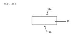
本発明は、1000℃より高い、好ましくはさらに1200℃より高い、1300℃より高い、1400℃より高い、又は1500℃より高い剥離温度で剥離可能な仮基板10に関する。剥離可能とは、仮基板10が、非常に高い温度で2つの部分に分離できること、この場合には、仮基板10の両方の部分である、加工層1をキャリア基板3から剥離することによって、前記加工層1を最終のレシーバ基板へ移動させることが可能であることを意味する。The present invention relates to a
仮基板10は、直径が100mm、150mm、200mm、又はさらに場合によっては450mmであり、典型的には300~800μmの厚さを有する、ウェハの形態で用意されることが好ましい。仮基板10は、図1a及び図1bに示されているように、主面(x、y)に沿って延在する、前面10a及び後面3bを有する。The
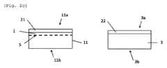
仮基板10は、中間層2上に配置された半導体加工層1を備え、中間層2自体は、キャリア基板3上に配置される。仮基板10はまた、中間層2内、又は中間層2と隣り合って位置する、すなわち、中間層2と加工層1との間又は中間層2とキャリア基板3との間に位置する、結合境界面4を有する。The
半導体材料でできた加工層1は、所与の用途に対処するために、部品をその中又は上に製造することが意図されている層である。仮基板10は、非常に高い処理温度を必要とする半導体材料に特に適しているので、加工層1は、炭化ケイ素を含んでおり有利である。加工層1はまた、もちろん、ダイヤモンド、たとえば窒化ガリウム若しくは窒化アルミニウムなどの、高い製造温度を必要とする2元若しくは3元のIII-V化合物、又は同様に高い処理温度若しくは製造温度(通常は1000°C若しくは1200°Cより高い)を必要とするII-VI化合物の中から選択される、1種又は複数の材料も含むことができる。The working
加工層1は、中間層2上に配置され、中間層2自体は仮基板10に備えられる。後者は、主平面(x、y)に垂直な軸線zに沿って、20nm未満、又はさらには10nm未満である、厚さを有する。この薄い厚さにより、たとえ中間層2の1種又は複数の構成材料が、剥離温度よりも低いクリープ又は溶融温度を有していても、仮基板10が、良好な機械的強度及び非常に高い温度との良好な適合性を保持できるという点で、重要である。The
中間層2は、主面(x,y)に平行に連続的に、又は不連続に、たとえば主面(x,y)に平行な面に並んで配置されたノジュールの形態で、延在してもよいことに留意されたい。It should be noted that the
中間層2は、たとえばタングステン、ニッケル、チタン、アルミニウム、モリブデン、タンタル、窒化チタン、窒化タンタル、及びアモルファスシリコンの中から選択される、少なくとも1種の金属又は半導体材料で形成されてもよい。The
中間層2の材料は、すなわち、加工層1の非常に薄い厚さ(10nm未満)にわたって、仮基板10を実現する、移動プロセス中に加えられる非常に高い温度で、加工層1に拡散及び/又は反応しないか、若しくはほとんど反応しないように選択される。これにより、加工層1の完全性及び純度を維持することができる。The material of the
中間層2は、キャリア基板3上に配置され、同様に、仮基板10の一部を形成する。キャリア基板3は、加工層1の処理に必要な又は目標となる高温に対応する、どんな材料で形成されてもよい。キャリア基板3は、その熱膨張係数が、加工層1の熱膨張係数に等しいか又は近い材料を含むことが好ましい。この材料は、たとえば、より低い結晶品質を示しながらも、加工層1と同じ性質であるように選択することができる。The
たとえば、加工層1が炭化ケイ素でできた特定の場合において、キャリア基板3自体は、加工層1よりも低い結晶品質の単結晶炭化ケイ素、又は多結晶炭化ケイ素で形成されてもよい。For example, in the particular case where the
仮基板10は、軸線zに沿った、最小濃度が1021/cm3よりも高い、濃度プロファイル2bに従って分布する、少なくとも1種の気体種の原子2aをさらに含む。 The
仮基板10を製造するプロセスでさらに詳細に説明されるように、この原子2aは、プロセスの様々な時点で、基板及び含まれる層の様々な場所に導入されてもよい。As will be described in more detail in the process of manufacturing the
したがって、原子2aの濃度プロファイル2bは、様々な形を取ってもよく、原子2aのほとんどが、中間層2に位置している一例が、図1bに示されている。別法として、原子2aのほとんどが、その厚さが10nm以下である、中間層2に隣り合うキャリア基板3の層内に位置してもよい。言い換えると、この場合、原子2aのほとんどが、キャリア基板3内に、ただし中間層2の非常に近くにある。さらに別の代替形態として、原子2aのほとんどが、その厚さが10nm以下である、中間層2に隣り合う加工層1の副層内に位置してもよい。The
原子2aの場所がどこであれ、濃度プロファイル2bは、原子2aの濃度が最大であり、1021/cm3以上、又はさらには数1021/cm3、通常は2E21/cm3~5E21/cm3の値に達する領域を、含む必要がある。 Wherever the
本発明によれば、原子2aは、仮基板10が剥離温度よりも低い温度に曝されているときには、中間層2、10nm以下の厚さを有するキャリア基板3の隣り合う層、及び/又は10nm以下の厚さを有する加工層1の隣り合う副層に閉じ込められた状態で保持されている。この原子2aは、仮基板10が剥離温度以上の温度に曝されると、中間層2内の又は中間層2に隣り合う、結合境界面4と一致するか又は結合境界面4の近傍の、剥離境界面に拡散することが意図されている。According to the invention, the
中間層2の材料及び気体種は、以下であるよう選択される。
原子のほとんどが、仮基板10が剥離温度よりも低い温度に曝されているとき、中間層2内の前記気体種の溶解度が高いことにより、中間層2に閉じ込められた状態で保持されるか、又は
原子のほとんどが、仮基板10が剥離温度よりも低い温度に曝されているとき、中間層2が、前記種に対して効果的なバリアを形成するので、キャリア基板3の隣り合う薄い層、及び/又は加工層1の隣り合う薄い副層に閉じ込められた状態で保持される。 The materials and gas species of the
Most of the atoms are either kept trapped in the
閉じ込められた原子2aのほとんどが、したがって、臨界温度(剥離温度)を超えると剥離境界面に蓄積し、仮基板10を使用する移動プロセスでさらに説明されるように、前記境界面に沿った剥離を引き起こす。Most of the trapped
気体種は、窒素、ヘリウム、アルゴン、キセノン、及び/又は水素の中から選択されることが好ましい。The gas species is preferably selected from nitrogen, helium, argon, xenon, and/or hydrogen.
ここで、仮基板10を製造するプロセスを、図2a~図2g、図3a、及び図3bを参照して説明することにする。The process for manufacturing the
製造プロセスは、最初に、前面11a及び後面11bを有するドナー基板11を用意するステップa)を含む(図2a)。ドナー基板11は、仮基板10の加工層1の元となり、したがって、少なくとも加工層1を形成する材料を含む。The manufacturing process first comprises step a) of providing a
ドナー基板11の前面11aの表面粗さは、原子間力顕微鏡(AFM:atomic force microscopy)を使って、20μm×20μmの走査により測定され、有利には、1nmRa(平均粗さ)未満となるよう選択される。The surface roughness of the
第1の選択肢によれば、ドナー基板11は、加工層1用に所望のレベルの品質を備えたバルク基板であり、この層は、ドナー基板11から直接もたらされる。According to a first option, the
第2の選択肢によれば、ステップa)は、ドナー基板11を形成するために、初期基板111にドナー層110をエピタキシャル成長させることを含む。ドナー層110は、初期基板111の結晶欠陥密度よりも低い結晶欠陥密度を有することが好ましい(図3a)。According to a second option, step a) comprises epitaxially growing a
ステップa)は、初期基板111及びドナー層110が炭化ケイ素でできている特定の場合には、初期基板111に単結晶変換層112を形成し、初期基板111の基底面転位欠陥を、ドナー層110のエピタキシャル成長の前に、貫通刃状転位欠陥に変換することを含んでもよい(図3b)。たとえば、ドナー層110で、1/cm2以下のBPD欠陥密度が目標となる。 Step a) may comprise, in the particular case where the
炭化ケイ素のエピタキシャル成長は、1200℃よりも高い温度、好ましくは1500℃~1650℃の温度で実行される。使用される前駆体は、モノシラン(SiH4)、プロパン(C3H8)又はエチレン(C2H4)であり、キャリアガスは、アルゴンを含むか又は含まない水素であってもよい。 The epitaxial growth of silicon carbide is carried out at temperatures above 1200° C., preferably between 1500° C. and 1650° C. The precursors used are monosilane (SiH4 ), propane (C3 H8 ) or ethylene (C2 H4 ), and the carrier gas may be hydrogen with or without argon.
ドナー層110(及び/又は変換層112)のエピタキシャル成長の前に、初期基板111の前面に存在する可能性がある微粒子、金属若しくは有機汚染物質、又は自然酸化物の層の全部又は一部を除去することを目的として、初期基板111を洗浄及び/又はエッチングする、従来のシーケンスを実行してもよいことに留意されたい。It should be noted that prior to epitaxial growth of the donor layer 110 (and/or the conversion layer 112), a conventional sequence may be performed to clean and/or etch the
製造プロセスは次に、前記ドナー基板11の埋込み脆弱面5を形成するために、水素、ヘリウム、又は両方の種の組合せの中から選択された軽イオンを、ドナー基板11(及び存在する場合は特に、ドナー層110に)に注入するステップb)を含む(図2b)。埋込み脆弱面5は、ドナー基板11の前面11aと共に、表面加工層1を画定する。The manufacturing process then comprises a step b) of implanting the donor substrate 11 (and, if present, the donor layer 110) with light ions selected from among hydrogen, helium or a combination of both species, in order to form a buried
スマートカット(商標)プロセスに関してよく知られているように、これらの軽い種が、注入深さの周囲に、ドナー基板11の前面11aに平行な、すなわち図の平面(x,y)に平行な薄い層に分布する、微小な空隙を形成することになる。この薄い層は、簡単にするために、埋込み脆弱面5と呼ばれる。As is well known for the Smart-Cut™ process, these light species will form tiny voids around the implantation depth, distributed in a thin layer parallel to the
軽い種の注入エネルギーは、ドナー基板11の決定された深さに到達するように選択され、この深さは、加工層1の目標厚さに一致する。たとえば、水素イオンでは、10keV~250keVのエネルギーで、5E16/cm2~1E17/cm2のドーズ量を注入されると、100~1500nm程度の厚さを有する加工層1を画定することになる。 The implantation energy of the light species is selected to reach a determined depth in the
軽い種のイオン注入のステップの前に、ドナー基板11の前面11aに、保護層が堆積されてもよいことに留意されたい。この保護層は、たとえば、シリコン酸化物又はシリコン窒化物などの材料で構成することができる。It should be noted that, prior to the step of ion implantation of light species, a protective layer may be deposited on the
仮基板10を製造するプロセスは、次に、キャリア基板3を用意することである、ステップc)を含む(図2c)。The process for manufacturing the
キャリア基板3は、上記で言及されたように、仮基板10に機械的支持をもたらし、所与の用途のために設計された最終的な複合構造体51に保持することを意図していない。したがって、キャリア基板3の主な特性は、低コスト、及び加工層1の機械的支持体としての信頼性であることが好ましい。The
製造プロセスは、次に、ドナー基板11及び/又はキャリア基板3に、少なくとも1つの膜21、22を堆積させるステップd)を含む(図2d)。言い換えると、第1の膜21が、ドナー基板11の前面11aに堆積されてもよく、代替的又は追加的に、第2の膜22が、キャリア基板3の前面3aに堆積されてもよい。図2dに示される例では、第1の膜21及び第2の膜22が、それぞれドナー基板11及びキャリア基板3に堆積される。The manufacturing process then comprises a step d) of depositing at least one
少なくとも1つの堆積された膜21、22は、仮基板10の中間層2を形成することを意図していることに留意されたい。Please note that at least one of the deposited
少なくとも1つの堆積膜21、22は、主平面(x、y)に垂直な軸線zに沿って、20nm未満、又はさらには10nm未満、たとえば0.3nm~10nmの厚さを有する。At least one of the deposited
少なくとも1つの膜21、22は、例として、タングステン、ニッケル、チタン、アルミニウム、モリブデン、タンタル、窒化チタン、窒化タンタル、アモルファスシリコンの中から選択される、少なくとも1種の材料で形成されてもよい。At least one of the
ステップd)の堆積は、特に直接液体噴射、プラズマ強化、熱、化学気相堆積(CVD:chemical vapour deposition)、スパッタリング又は蒸着による堆積など、任意の既知の技法を使用して実行されてもよい。The deposition of step d) may be carried out using any known technique, such as direct liquid injection, plasma-enhanced, thermal, chemical vapor deposition (CVD), sputtering or evaporation deposition, among others.
製造プロセスは、次に、ドナー基板11とキャリア基板3とを接合し、これにより少なくとも1つの膜21、22が前記基板11,3の間に配置され、中間層2を形成するステップe)を含む(図2e)。The manufacturing process then includes step e) of bonding the
ドナー基板11及びキャリア基板3は、これらのそれぞれの前面11a、3aで接合され、積層体311を形成する。2つの基板は、それ自体はよく知られているように、分子接着による、すなわち、この場合、基板11、3の前面を、面の一方又は両方に膜21、22が設けられた状態で、直接接触させて配置することによる、直接結合を使用して接合されてもよい。結合は、周囲温度又は800℃未満の温度で、大気中又は制御された雰囲気、たとえば真空下で行うことができる。The
ステップe)は、この接触の前に、結合境界面4の品質を向上させることができる(低い欠陥密度、良好な接着品質)、洗浄、表面活性化、又は他の表面処理の、従来のシーケンスを含んでもよい。Step e) may include a conventional sequence of cleaning, surface activation or other surface treatments prior to this contacting, which can improve the quality of the bonding interface 4 (low defect density, good adhesion quality).
接合又は結合境界面4は、中間層2内、中間層2と加工層1との間、又はさもなければ中間層2とキャリア基板3との間に位置する。The bonding or joining
製造プロセスは、次に、埋込み脆弱面5に沿って分離させ、一方で仮基板10を形成し、他方でドナー基板の残りの部分11’を形成することを含む、ステップf)を含む(図2f)。仮基板10の前面10aはまた、ドナー基板11から生じる加工層1の前面でもある。The manufacturing process then includes a step f) (FIG. 2f), which involves a separation along the embedded
1つの有利な実施態様によれば、分離させるステップf)は、積層体311に、分離温度で熱処理を加えることにより実行される。埋込み脆弱面5に存在する微小な空隙は、分割波が始まるまで成長速度に従い、分割波は、埋込み脆弱面5の全範囲にわたって伝播し、その結果ドナー基板の残りの部分11’から仮基板10が分離される。実際には、炭化ケイ素でできたドナー基板11では、温度は、ステップb)の注入条件に応じて、900℃~1200℃であってもよい。According to one advantageous embodiment, the separation step f) is carried out by subjecting the
1つの代替の実施態様によれば、分離ステップf)は、900℃~1200℃の温度での熱処理の全体又は一部が完了した後に、積層体311に機械的ストレスを加えることによって実行される。ストレスは、たとえば、埋込み脆弱面5の近傍に工具(たとえば剃刀の刃)を挿入することによって、加えることができる。分離ストレスは、例として、数GPa程度、好ましくは2GPaよりも大きくてもよい。According to one alternative embodiment, the separation step f) is performed by applying a mechanical stress to the laminate 311 after the heat treatment at a temperature between 900° C. and 1200° C. has been completed in whole or in part. The stress can be applied, for example, by inserting a tool (for example a razor blade) in the vicinity of the embedded
それ自体知られているように、分離ステップf)の終了時に、仮基板10の加工層1の前面10aは、5~100nm RMSの表面粗さを有する(原子間力顕微鏡(AFM)を使った、20μm×20μmの走査により測定される)。In a manner known per se, at the end of the separation step f), the
ステップf)は、任意選択で、分離後、加工層1を平滑化及び修復する処理を含んでもよい。特に、制御された(酸化若しくは還元する)雰囲気下での熱処理、加工層1の損傷した表面部分を除去するための、湿式若しくは乾式化学エッチング、及び/又は良好なレベルの粗さ(たとえば、20×20μmのAFMの範囲で0.5nm RMS未満、若しくはさらには0.3nm未満の、最終的な粗さ)を復元し、場合によっては損傷した表面部分を除去するための、加工層1の前面の化学機械研磨について、言及することができる。仮基板10に、従来の洗浄シーケンス、たとえば、SC1/SC2タイプ(標準洗浄1、標準洗浄2)、HF(フッ化水素酸)、及び/又はN2、Ar、CF4などを用いたプラズマでの洗浄もまた適用して、加工層1の前面10aの品質をさらに高めることができる。 Step f) may optionally include a treatment to smooth and repair the working
キャリア基板3は、加工層1に適合し、機械的に、また高温で安定するよう選択され、また中間層2は、非常に薄い厚さになるよう選択されるので、加工層1に高品質を取り戻すために必要な熱的、機械的、又は化学的処理を、加工層1への望ましからざるストレス又は損傷のリスクなしに、仮基板10へ容易に加えることができる。The
ステップf)の後に、仮基板10の加工層1に追加層をエピタキシャル成長させるステップを続けることができることに留意されたい。かかるステップは、加工層に、相対的にかなりの厚さ、典型的には数ミクロンから数十ミクロン程度、たとえば5μm~50μmが必要な場合に適用される。エピタキシ温度は、仮基板10の剥離が時期尚早に開始されるのを回避するために、有利には、1500℃より低く、又はさらには1300℃より低くなるよう選択される。It should be noted that step f) can be followed by a step of epitaxially growing an additional layer on the working
中間層2は、高温熱処理を含むことが好ましいステップf)の間又は終了時に、物理的及び/又は形態学的変化を起こすことがある。少なくとも1つの膜21、22は、加工層1の材料とキャリア基板3の材料との間の連続領域に、層間挿入されたノジュールを形成する可能性があり、中間層2は、この場合、ノジュールの不連続層で形成される。したがって、接合境界面4自体もまた実質的に変化し、ノジュール内、ノジュールと加工層1との間、ノジュールとキャリア基板3との間、並びに/又は加工層1とキャリア基板3との間に位置することがある。別法として、中間層2は、接合境界面4に沿ってずっと、中間層2の連続形態を保持していてもよい。The
製造プロセスは、少なくとも1種の気体種の原子2aを、少なくとも1つの膜21、22、又はその近傍に導入するステップをさらに含む。気体種は、上記の仮基板10の説明で言及したように、窒素、ヘリウム、アルゴン、キセノン、及び/又は水素であってもよい。この気体種の原子2aは、中間層2、10nm以下の厚さを有するキャリア基板3の隣り合う層、及び/又は10nm以下の厚さを有する加工層1の隣り合う副層に、閉じ込められることを意図したものである。The manufacturing process further comprises the step of introducing
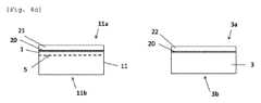
図4-1、図4d、図4e、及び図4fに示されている第1の実施態様において、原子2aを導入するこのステップは、膜21、22を堆積させるステップd)の前に実行されるので、-1)と呼ぶことにする。原子2aは、ドナー基板11及び/又はキャリア基板3に、それぞれの前面11a、3aから、10nm未満の浅い深さまで導入される。イオン注入は、原子2aをイオンの形態で、1つ又は複数の基板11、3に導入するために実行することができ、イオン注入エネルギーは、典型的には、10keVよりも小さく、又はさらには5keVよりも小さく、注入ドーズ量は、典型的には、2E15/cm2~数1E16/cm2である。したがって、注入ゾーン20は、ドナー基板11の前面11aの表面近傍、及び/又はキャリア基板3の前面3aの表面近傍に形成される。 In a first embodiment shown in Figures 4-1, 4d, 4e and 4f, this step of introducing
プロセスのステップd)~f)は、この場合、上記で説明されたように実行され、図4d、図4e、図4fに示されている。Process steps d) to f) are in this case carried out as described above and are illustrated in Figures 4d, 4e and 4f.
原子2aは、中間層2に隣り合うキャリア基板3の薄い層(厚さ10nm以下)内、及び中間層2に隣り合う加工層1の薄い副層(厚さ10nm以下)内に位置し、前記隣り合う層及び副層は、注入ゾーン20から始まる。原子2aは、気体種及び中間層2の性質に応じて、仮基板10に熱処理が加えられる間、後者が、ステップf)の分離温度よりも著しく高い、剥離温度以上の温度に曝されない限り、前述の層及び副層に閉じ込められた状態で保持されるか、又は中間層2に閉じ込められた状態になる可能性がある。The
気体種の原子2aは、主平面(x、y)に垂直な軸線zに沿った濃度プロファイルに従って分布し、最大濃度は1021/cm3よりも高い。 The
図5-1に示されている第2の実施態様において、原子2aを導入するステップは、膜21、22を堆積させるステップd)の後に実行されるので、-1)と呼ぶことにする。In the second embodiment shown in FIG. 5-1, the step of introducing
少なくとも1つの膜21、22は、上記で言及されたように、ドナー基板11上及び/又はキャリア基板3上に存在してもよい。At least one
原子2aは、少なくとも1つの膜21、22に導入される。イオン注入は、原子2aをイオンの形態で導入するために実行することができ、イオン注入エネルギーは、ステップd)で堆積される膜21、22の厚さに応じて、典型的には10keVよりも小さく、又はさらには5keVよりも小さい。注入ドーズ量は、典型的には、2E15/cm2~数1E16/cm2である。 The
気体種の原子2aは、中間層2内で、軸線zに沿った濃度プロファイルに従って分布し、最大濃度は、注入ピークに位置し、1021/cm3よりも高い。 The
プロセスのステップe)~f)は、この場合、上記で説明されたように実行される(図2e、図2f)。Process steps e) to f) are then carried out as described above (Figures 2e, 2f).
図6-1に示されている第3の実施態様において、原子2aを導入するステップは、分離ステップf)の後に実行されるので、-1)と呼ぶことにする。In the third embodiment shown in Figure 6-1, the step of introducing
原子2aは、たとえばイオン注入によって、中間層2に導入される。イオン注入エネルギーは、この場合、イオンが通過して中間層2に到達する、加工層1の性質及び厚さに依存する。注入ドーズ量は、典型的には、2E15/cm2~数1E16/cm2である。 The
気体種の原子2aは、この場合も、軸線zに沿った濃度プロファイルに従って分布し、最大濃度は、注入ピークに位置し、1021/cm3より高いと予測される。 The
説明された3つの実施態様のいずれにおいても、注入されるイオンの総ドーズ量は、完成した仮基板10において、原子2aの濃度プロファイルが1021/cm3よりも高い最大濃度を示すように定められる。 In all three described embodiments, the total dose of implanted ions is determined so that in the completed
気体種の原子2aの大きいドーズ量を、中間層2内及び/又は中間層2の非常に近くに導入することにより、下記で説明される本発明の移動プロセス中に、中間層2内又は中間層2に隣り合う剥離境界面を生成することが可能になる。By introducing a large dose of
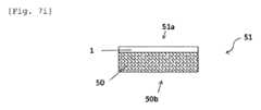
本発明はまた、加工層1を上記で説明された仮基板10からレシーバ基材50に移動させるプロセスにも関する。移動プロセスは、図7g~図7jを参照して説明される。The present invention also relates to a process for transferring the
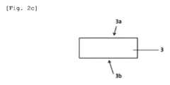
レシーバ基板50は、直径が100mm、150mm、200mm、又は場合によってはさらに450mmであり、典型的には300~800μmの厚さを有する、ウェハの形態で用意されることが好ましい。レシーバ基板50は、互いに反対側にある、前面及び後面50bを備える。レシーバ基板50は、最終用途向けに設計されており、したがって、レシーバ基板50の物理的及び電気的特性は、特に必要な仕様に合わせて選択される。The
加工層1が、たとえば高い結晶品質の炭化ケイ素でできているパワーエレクトロニクス用途では、レシーバ基板50は、特に多結晶炭化ケイ素でできており、垂直方向の導電経路を備えるために、良好な導電性を示すことができる。In power electronics applications, where the
移動プロセスは、仮基板10の加工層1上に配置されたレシーバ基板50を備える、剥離可能な構造体510を形成するステップg)を含む(図7g)。図7gの仮基板10が、中間層2に閉じ込められた気体種の原子2aと共に示されていることに留意されたい。原子2aが別の場所にある、上記で説明された他のどんな構成も、もちろん実施することができる。The transfer process includes step g) of forming a peelable structure 510 comprising a
ステップg)は、1000℃以上、且つ有利には1500℃以下である、第1の温度での処理を含む。Step g) involves treatment at a first temperature, which is greater than or equal to 1000°C and preferably less than or equal to 1500°C.
第1の実施形態によれば、ステップg)は、仮基板10の加工層1の自由面10aへの、レシーバ基板50の堆積を含む。堆積は、特に、高品質の多結晶炭化ケイ素でできたレシーバ基板50を、非常に高品質の単結晶炭化ケイ素でできた加工層1に堆積することが望まれる場合、1000℃より高いか、1200℃以上か、又はさらには1400℃より高い温度(第1の温度に一致する)で実行されてもよい。もちろん、レシーバ基板50を形成するための、非常に高い温度で堆積される他の材料が、興味深い場合がある。According to a first embodiment, step g) comprises the deposition of a
加工層1とレシーバ基板50との間の導電を必要とする用途では、これらの間に非絶縁性の境界面を画定しなければならない。言い換えると、ステップg)は、加工層1とレシーバ基板50との境界面が導電性になるように実行される。境界面の比抵抗は、典型的には、1mΩ・cm2未満が目標となる。加工層1の自由面10a上に存在する自然酸化物の除去が、境界面の導電性を確保するために、湿式又は乾式ルートでのHF(フッ化水素酸)脱酸によって実行されるので有利である。別法として、堆積されたレシーバ基板50の最初の数ナノメートルの過剰ドーピングにより、加工層1と前記基板50との境界面の導電性を高めてもよい。 In applications requiring electrical conductivity between the working
また、脱酸及び/又はレシーバ基板50形成の前に、仮基板10に洗浄シーケンスを施し、仮基板10の自由面10a、3bに存在する可能性がある微粒子、金属又は有機汚染物質の全部又は一部を除去するので有利である。It is also advantageous to subject the
第1の実施形態では、仮基板10の加工層1は、ステップf)の分離後に、仮基板10の表面粗さを完全に復元するために、必ずしも研磨する必要がないことに留意されたい。非常に高い温度(典型的には1100℃~1500℃)での堆積又はエピタキシによるレシーバ基板50の製造は、加工層1の表面の修復及び再構成を促すことができ、さらに、残留した粗さを許容することができる。It should be noted that in the first embodiment, the working
キャリア基板3は、加工層1に適合し、機械的に、また高温で安定するよう選択され、また中間層2は、非常に薄い厚さになるよう選択されるので、剥離可能な構造体510を形成するために必要な熱的、機械的、又は化学的処理を、加工層1への望ましからざるストレス又は損傷のリスクなしに、仮基板10へ容易に加えることができる。The
この第1の実施形態では、ステップg)の堆積は、蒸着又は化学気相堆積(CVD)技法を使用して実行されてもよい。大気圧CVD(APCVD:atmospheric-pressure CVD)若しくは低圧CVD(LPCVD:low-pressure CVD)などの熱CVD技法、プラズマ励起CVD(PECVD:plasma-enhanced CVD)、又はさもなければ直接液体噴射式CVD(DLI-CVD:direct-liquid-injection CVD)が使用されてもよい。In this first embodiment, the deposition of step g) may be carried out using evaporation or chemical vapor deposition (CVD) techniques. Thermal CVD techniques such as atmospheric-pressure CVD (APCVD) or low-pressure CVD (LPCVD), plasma-enhanced CVD (PECVD) or else direct-liquid-injection CVD (DLI-CVD) may be used.
前述のパワー用途に必要な導電特性を得るために、炭化ケイ素でできたレシーバ基板50の例に戻ると、基板は、たとえば、以下の構造上の特性を示すことができる。多結晶構造、3C SiCタイプの粒子、111配向、平均サイズは1~50μm、最終抵抗率が0.03ohm・cm以下のn型ドーピング。Returning to the example of a
レシーバ基板50は、ステップg)の終了時に、典型的には50μm以上の厚さ、又はさらには、100μm以上の厚さ、たとえば300μm程度の厚さを有する。ステップg)から得られる剥離可能な構造体510は、加工層1上に配置されたレシーバ基板50を備え、加工層1自体は、仮基板10内に備えられる。レシーバ基板50を製造するために実現される第1の温度は、剥離温度よりも低く、したがって、気体種の原子2aのほとんどが、中間層2、10nm以下の厚さを有するキャリア基板3の隣り合う層、及び/又は10nm以下の厚さを有する加工層1の隣り合う副層に、閉じ込められた状態で保持される。At the end of step g), the
レシーバ基板50がバルク基板である第2の実施形態によれば、ステップg)は、前記レシーバ基板50を、仮基板10の加工層1の自由面10aに接合して、剥離可能な構造体510を形成する工程を含む。According to a second embodiment in which the
接合工程は、任意の既知の技法を使用して、特に、分子接着による直接結合、熱圧着接合、又は非常に高い温度に対応する、別のタイプの結合を使用して、実行されてもよい。ステップg)は、この結合を強固にするために、1000℃以上、又はさらには1200℃以上の温度(第1の温度に一致する)での熱処理をさらに含む。The bonding process may be carried out using any known technique, in particular direct bonding by molecular adhesion, thermocompression bonding or another type of bonding compatible with very high temperatures. Step g) further comprises a heat treatment at a temperature of 1000°C or higher, or even 1200°C or higher (corresponding to the first temperature), in order to consolidate this bond.
本発明による移動プロセスは、次に、中間層2内又は中間層2に隣り合って位置する剥離境界面に沿って、剥離可能な構造体510を剥離するステップh)を含む。このステップは、一方で、レシーバ基板50上に配置された加工層1を備える複合構造体51を形成し、他方で、キャリア基板3を形成する(図7h)。剥離ステップは、ステップf)の分離温度よりも高く、ステップg)で加えられる第1の温度よりも高い剥離温度での、熱処理を含む。剥離温度は、1000℃より高い。The transfer process according to the invention then comprises a step h) of peeling the peelable structure 510 along a peel interface located in or adjacent to the
中間層2が、窒素の原子2aが注入されたタングステンを含み、加工層1及びキャリア基板3が、SiCでできた特定の場合において、剥離温度は、典型的には、1400℃以上、又はさらには1500℃以上、たとえば1600℃又は1700℃にすることができる。In the particular case where the
仮基板10内に存在する原子2aは、ステップh)の熱処理の過程にわたって移行し、中間層2内又は中間層2に隣り合う接合境界面4と一致するか又は接合境界面4近傍の、剥離境界面に蓄積する。気体種は、次いで、加圧された微小な亀裂を生成し、微小な亀裂は、圧力下で増大して、剥離可能な構造体510の内部で、剥離可能な構造体510の主面(x、y)に平行な全エリアにわたって、剥離を引き起こす。
1つの特定の実施形態によれば、中間層2は、ステップh)の間又は事前の先立つ熱処理の間に、ノジュールの形態へのセグメント化を起こす。このノジュールは、この場合、加工層1の材料とキャリア基板3の材料との間の連続領域に、層間挿入される。ステップh)で起こる気体種の蓄積は、この場合、前記連続領域で優先的に生じ、加圧された微小な亀裂を引き起こす。According to one particular embodiment, the
本発明による移動プロセスにおける剥離現象は、仮基板10又は剥離可能な構造体510に事前に加えられる非常に高い温度よりも高い、剥離温度でしか起こらないので、特に有利であり、したがって、前記剥離可能な構造体510を形成するための、いくつかのタイプのステップの利用が可能となる。高い第1の温度により、特に、非常に高品質のレシーバ基板50(第1の実施形態において)、及び/又はレシーバ基板50の加工層1への非常に高品質の接合(第2の実施形態において)を、中間層2での剥離境界面の早すぎる進行を引き起こすことなく、達成することができる。The delamination phenomenon in the transfer process according to the invention is particularly advantageous since it only occurs at delamination temperatures higher than the very high temperatures previously applied to the
したがって、第2段階で、より高い剥離温度で、剥離可能な構造体510の剥離を引き起こし、複合構造体51を形成することが可能である。Therefore, in the second stage, it is possible to induce peeling of the peelable structure 510 at a higher peeling temperature to form a
本発明による移動プロセスは、次に、加工層1の自由面である、複合構造体51の前面51aの化学洗浄、化学エッチング、及び/又は化学機械研磨の工程を含む、複合構造体51を仕上げるステップi)を含んでもよい。化学エッチング又は研磨は、複合構造体51の前面51aから、中間層2’の残留物を除去するのに有用な場合があることに留意されたい。The transfer process according to the invention may then include a step i) of finishing the
ステップi)はまた、レシーバ基板50の自由面50bである、複合構造体51の後面50bに施される化学洗浄、化学エッチング、機械研削、及び/又は化学機械研磨の工程を含んでもよい。Step i) may also include chemical cleaning, chemical etching, mechanical grinding, and/or chemical-mechanical polishing processes applied to the
特にレシーバ基板50が堆積によって形成される第1の実施形態において、縁部の環状の輪郭及び縁部の屑の形状を、マイクロエレクトロニクス製造プロセスの要件に適合したものにするための、複合構造体51の縁部の研磨又は研削もまた、このステップi)の間に実行されてもよい。Polishing or grinding of the edge of the
ステップi)は、最後に、複合構造体51の加工層1の追加層のエピタキシャル成長を含んでもよい。かかるステップは、一時的な基板10から移動された加工層1の厚さが、部品の製造に十分でない場合か、又は特定のドーピングタイプ若しくは特定の組成を有する層が、前記部品の加工表面1に必要な場合に、適用される。Step i) may finally comprise the epitaxial growth of an additional layer of the working
移動プロセスは、任意選択で、剥離ステップh)の前に、レシーバ基板50の後面50bの化学洗浄、化学エッチング、機械研削、及び/又は化学機械研磨、並びに場合によっては、剥離可能な構造体510の縁部の研削の工程を含む、剥離可能な構造体510を処理するステップg’)を含んでもよい。これにより、剥離可能な構造体510に依然として埋め込まれている加工層1を損傷するリスクなしに、レシーバ基板50の形状及び厚さを処理及び改良することが可能となる。Optionally, the transfer process may include a step g') of processing the releasable structure 510 prior to the peeling step h), including chemical cleaning, chemical etching, mechanical grinding, and/or chemical-mechanical polishing of the
本発明による移動プロセスは、最後に、特に新しい仮基板10のキャリア基板として再利用するために、キャリア基板3を再調整するステップj)を含んでもよい(図7j)。かかる再調整のステップは、ステップh)の終了時の、表面又は縁部の化学機械研磨、機械研削、及び/又は湿式若しくは乾式化学エッチングによる、基板3の前面の1つ又は複数の処理をベースとする。The transfer process according to the invention may finally comprise a step j) of reconditioning the
(例示的な実施態様)
非限定的で例示的な一実施態様によれば、製造プロセスのステップa)で用意される初期基板111は、4H型結晶多形のc-SiCでできたウェハであり、軸線<11-20>に対して4.0°±0.5°の方位を有し、直径150mm及び厚さ350μmである。RCAタイプ(標準洗浄1+標準洗浄2)、次いでカロ酸(硫酸と過酸化水素との混合物)、次いでHF(フッ化水素酸)の、従来の洗浄シーケンスが、初期基板111で、c-SiCでできたドナー層110のエピタキシャル成長の前に実行される。Illustrative Embodiments
According to one non-limiting exemplary embodiment, the
成長は、エピタキシ用チャンバで、1650°Cの温度で、モノシラン(SiH4)及びプロパン(C3H8)又はエチレン(C2H4)などの前駆体を使用して実行され、厚さ30μmのc-SiCドナー層110を生成する(成長速度は、10μm/時)。ドナー層110は、1/cm2程度のBPD欠陥密度を有する。 The growth is carried out in an epitaxy chamber at a temperature of 1650° C. using precursors such as monosilane (SiH4 ) and propane (C3 H8 ) or ethylene (C2 H4 ), producing a 30 μm thick c-SiC donor layer 110 (
ステップb)で注入される水素イオンは、150keVのエネルギー及び6E16 H+/cm2のドーズ量で、ドナー層110の自由表面を通して注入される。このようにして、ドナー層110の約800nmの深さで、埋込み脆弱面5が生成される。 The hydrogen ions implanted in step b) are implanted through the free surface of the
ステップc)で、直径150mm、厚さ550μmの低い結晶品質の単結晶炭化ケイ素でできたキャリア基板3を用意する。In step c), a
RCAタイプ+カロ酸の洗浄シーケンスが、ドナー基板11及びキャリア基板3に施され、ドナー基板11及びキャリア基板3の自由面から、可能性のある汚染物質が除去される。An RCA type + Caro's acid cleaning sequence is applied to the
第1の膜21及び第2の膜22を形成するために、タングステンが、ドナー基板11の前面11a及びキャリア基板3の前面3aに、700℃程度の温度での化学気相蒸着を使用して、0.5nmの厚さで堆積される(ステップd))。To form the
膜21に注入ピーク(最大濃度)を入れるために、窒素が、5keVの注入エネルギー及び1E16/cm2のドーズ量で、ドナー基板11の膜21に注入される(ステップ-1))。 Nitrogen is implanted into the
次に、ステップe)が、積層体311を形成するために、ドナー基板11の注入された膜21の、接合境界面4に沿った、キャリア基板3の膜22への分子接着による接合を実現する。2つの膜21、22は、中間層2を形成する。Next, step e) realizes the bonding by molecular adhesion of the implanted
分離ステップf)は、埋込み脆弱面5に沿って、950℃で数十分間又はさらには1時間の熱処理を加えることにより行われる。このようにして、表面加工層1を有する仮基板10が形成される。ドナー基板11’の残りの部分は、再調整して、新しいサイクルで再使用されてもよい。The separation step f) is carried out by applying a heat treatment at 950° C. for several tens of minutes or even an hour along the buried
1000℃以上の温度での、前記加工層1を修復するための熱処理のみならず、加工層1の表面から約200nmを除去する化学機械研磨の工程も実行される。気体種の原子2aのほとんどが、このステップの間、中間層2に閉じ込められた状態で保持される。Not only is a heat treatment at a temperature of 1000°C or higher performed to repair the processed
複合構造体51を製造するために、加工層1をレシーバ基板50に移動させる目的で、多結晶炭化ケイ素のLP-CVD堆積の工程が、仮基板10の加工層1で、メチルシラン前駆体を用いて、1250℃の温度で120分間、レシーバ基板50の厚さが360μmに達するように実行される。レシーバ基板50は、これらの条件下で、非常に高品質の多結晶である(ステップg))。レシーバ基板50の厚さ、及び場合によってはレシーバ基板50の周縁の形状を調整するために、研削及び/又は研磨のステップを実行することができる。このようにして、剥離可能な構造体510が生成される。For the purpose of transferring the working
剥離ステップh)は、剥離可能な構造体510に加えられる、1700℃での熱処理に対応する。中間層2に閉じ込められた窒素の原子2aの拡散、及び結合境界面4又は結合境界面4の非常に近くでの、加圧された微小な亀裂を形成するための原子2aの蓄積によって生じる剥離境界面が、剥離可能な構造体510の完全な剥離を引き起こすまで、中間層2内に形成される。このようにして、一方で、レシーバ基板50上に配置された加工層1を備える複合構造体51と、他方で、キャリア基板3とが得られる。複合構造体51及びキャリア基板3はそれぞれ、たとえば研磨又は化学エッチングによって除去することができる、中間層2の残留物2’、2’’を備える。The peeling step h) corresponds to a heat treatment at 1700 ° C. applied to the peelable structure 510. A peeling interface is formed in the
機械研削又は化学機械研磨が、剥離可能な構造体510で実行されなかった場合、複合構造体51の後面に施すことが好ましい。If mechanical grinding or chemical-mechanical polishing has not been performed on the peelable structure 510, it is preferable to apply it to the rear surface of the
原則として、加工層1の自由面51aに相当する、前記構造体51の前面51aは、一時的な基板10の層の品質及び前面51aの低い粗さが得られたので、従来の洗浄を必要としない。In principle, the front surface 51a of the
次に、場合によっては、加工層1での追加層のエピタキシャル成長の後に、複合構造体51上に、垂直方向の部品が製造されてもよい。Vertical components may then be manufactured on the
上記の例で説明されたものと同様の条件下で、少なくとも1つの膜21、22の材料は、アモルファスシリコンであってもよく、導入される原子2aは、アルゴン又はヘリウムであってもよい。Under conditions similar to those described in the above example, the material of at least one of the
言うまでもなく、本発明は、説明された実施形態及び例に限定されるものではなく、特許請求の範囲によって定められる本発明の範囲から逸脱することなく、実施態様の変形が本発明に加えられてもよい。Needless to say, the invention is not limited to the described embodiments and examples, and variations in implementation may be made to the invention without departing from the scope of the invention as defined by the claims.
Claims (15)
Translated fromJapanese主平面(x,y)に沿って延在する、半導体加工層(1)と、
キャリア基板(3)と、
前記加工層(1)と前記キャリア基板(3)との間に配置され、前記主平面(x、y)に垂直な軸線(z)に沿って20nm未満の厚さを有する、中間層(2)と、
前記中間層(2)内又は前記中間層(2)に隣り合って位置する、結合境界面(4)と、
最大濃度が1021/cm3を超え、前記主平面(x,y)に垂直な前記軸線(z)に沿った濃度プロファイル(2b)に従って分布する少なくとも1種の気体種の原子(2a)であり、前記原子(2a)が、前記仮基板(10)が前記剥離温度より低い温度に曝されているとき、前記中間層(2)、10nm以下の厚さを有する前記キャリア基板(3)の隣り合う層、及び/又は10nm以下の厚さを有する前記加工層(1)の隣り合う副層に閉じ込められた状態で保持され、前記原子(2a)が、前記仮基板(10)が前記剥離温度以上の温度に曝されると、剥離境界面に拡散するよう意図されている、原子(2a)と、
を備える、仮基板(10)。 A temporary substrate (10) that can be peeled off at a peeling temperature exceeding 1000°C, the temporary substrate (10) comprising:
A semiconductor processing layer (1) extending along a major plane (x, y);
A carrier substrate (3),
an intermediate layer (2) arranged between the processing layer (1) and the carrier substrate (3) and having a thickness along an axis (z) perpendicular to the main plane (x, y) of less than 20 nm;
a bonding interface (4) located within or adjacent to said intermediate layer (2);
atoms (2a) of at least one gaseous species with a maximum concentration of more than 1021 /cm3 and distributed according to a concentration profile (2b) along said axis (z) perpendicular to said main planes (x, y), said atoms (2a) being kept confined in said intermediate layer (2), in adjacent layers of said carrier substrate (3) having a thickness of 10 nm or less and/or in adjacent sublayers of said processing layer (1) having a thickness of 10 nm or less when said temporary substrate (10) is exposed to a temperature below said delamination temperature, said atoms (2a) being intended to diffuse to the delamination interface when said temporary substrate (10) is exposed to a temperature above said delamination temperature;
A temporary substrate (10).
a)ドナー基板(11)を用意するステップと、
b)前記ドナー基板(11)内に埋込み脆弱面(5)を形成するために、水素、ヘリウム、又はこれら2つの組合せの中から選択された軽イオンを前記ドナー基板(11)に注入するステップであり、前記埋込み脆弱面(5)が、前記ドナー基板(11)の前面(11a)と共に、表面加工層(1)を画定する、注入するステップと、
c)前面(3a)を有するキャリア基板(3)を用意するステップと、
d)前記ドナー基板(11)の前記前面(11a)及び/又は前記キャリア基板(3)の前記前面(3a)に、前記中間層(2)を形成するよう意図されている少なくとも1つの膜(21、22)を堆積させるステップと、
e)前記少なくとも1つの膜(21、22)が前記基板(11),(3)の間に配置されて、前記中間層(2)を形成するように、前記ドナー基板(11)と前記キャリア基板(3)とを接合するステップと、
f)一方で前記仮基板(10)を形成し、他方で前記ドナー基板の残りの部分(11’)を形成するために、前記埋込み脆弱面(5)に沿って分離するステップと、を含み、
前記製造するプロセスが、
堆積させるステップd)の前に、前記ドナー基板(11)及び/若しくは前記キャリア基板(3)の、それぞれの前面(11a、3a)から10nm以下の深さまで、
堆積させるステップd)の後に、前記少なくとも1つの膜(21、22)内へ、又は
分離するステップf)の後に、前記中間層(2)内へ、
前記少なくとも1種の気体種の原子(2a)を導入するステップをさらに含む、仮基板(10)を製造するプロセス。 A process for manufacturing a temporary substrate (10) according to any one of claims 1 to 4, said process comprising:
a) providing a donor substrate (11);
b) implanting the donor substrate (11) with light ions selected from hydrogen, helium or a combination of the two, in order to form a buried weak surface (5) in the donor substrate (11), the buried weak surface (5) defining, together with the front surface (11a) of the donor substrate (11), a surface engineered layer (1);
c) providing a carrier substrate (3) having a front surface (3a);
d) depositing on said front surface (11a) of said donor substrate (11) and/or on said front surface (3a) of said carrier substrate (3) at least one film (21, 22) intended to form said intermediate layer (2);
e) bonding the donor substrate (11) and the carrier substrate (3) such that the at least one film (21, 22) is disposed between the substrates (11), (3) to form the intermediate layer (2);
f) separating along said buried weak surface (5) to form, on the one hand, said temporary substrate (10) and, on the other hand, the remaining part of the donor substrate (11'),
The manufacturing process comprises:
Prior to the depositing step d), from the respective front surface (11a, 3a) of the donor substrate (11) and/or the carrier substrate (3) to a depth of 10 nm or less,
into said at least one membrane (21, 22) after the depositing step d), or into said intermediate layer (2) after the separating step f),
The process for producing a temporary substrate (10), further comprising the step of introducing atoms (2a) of said at least one gaseous species.
g)前記仮基板(10)の前記加工層(1)上に配置されたレシーバ基板(50)を備える、剥離可能な構造体(510)を形成するステップであり、1000℃以上の第1の温度で処理することを含む前記形成するステップと、
h)前記中間層(2)内又は前記中間層(2)に隣り合う剥離境界面に沿って前記剥離可能な構造体(510)を剥離するステップであり、一方で前記レシーバ基板(50)上に配置された前記加工層(1)を備える複合構造体(51)と、他方で前記キャリア基板(3)とを形成するために、前記第1の温度よりも高い剥離温度で熱処理することを含む前記剥離するステップと、
を含む、仮基板(10)から加工層(1)を移動させるプロセス。 A process for transferring a working layer (1) from a temporary substrate (10) according to any one of claims 1 to 4 to a receiver substrate (50), comprising the steps of:
g) forming a peelable structure (510) comprising a receiver substrate (50) disposed on the working layer (1) of the temporary substrate (10), said forming step including treating at a first temperature of 1000° C. or higher;
h) peeling the peelable structure (510) along a peel interface in or adjacent to the intermediate layer (2), said peeling step comprising a heat treatment at a peel temperature higher than said first temperature to form a composite structure (51) comprising the working layer (1) arranged on the receiver substrate (50) on the one hand and the carrier substrate (3) on the other hand;
A process for transferring a working layer (1) from a temporary substrate (10), comprising:
Applications Claiming Priority (3)
| Application Number | Priority Date | Filing Date | Title |
|---|---|---|---|
| FR2006023 | 2020-06-09 | ||
| FR2006023AFR3111232B1 (en) | 2020-06-09 | 2020-06-09 | REMOVABLE TEMPORARY SUBSTRATE COMPATIBLE WITH VERY HIGH TEMPERATURES AND METHOD FOR TRANSFERRING A USEFUL LAYER FROM SAID SUBSTRATE |
| PCT/FR2021/050718WO2021250333A1 (en) | 2020-06-09 | 2021-04-26 | Detachable temporary substrate compatible with very high temperatures and process for transferring a working layer from said substrate |
Publications (2)
| Publication Number | Publication Date |
|---|---|
| JP2023528784A JP2023528784A (en) | 2023-07-06 |
| JP7620646B2true JP7620646B2 (en) | 2025-01-23 |
Family
ID=72266550
Family Applications (1)
| Application Number | Title | Priority Date | Filing Date |
|---|---|---|---|
| JP2022572577AActiveJP7620646B2 (en) | 2020-06-09 | 2021-04-26 | A peelable temporary substrate capable of handling very high temperatures and a process for transferring a working layer from said substrate - Patents.com |
Country Status (8)
| Country | Link |
|---|---|
| US (1) | US20230230868A1 (en) |
| EP (1) | EP4162522B1 (en) |
| JP (1) | JP7620646B2 (en) |
| KR (1) | KR102857900B1 (en) |
| CN (1) | CN115715425A (en) |
| FR (1) | FR3111232B1 (en) |
| TW (1) | TWI872240B (en) |
| WO (1) | WO2021250333A1 (en) |
Families Citing this family (3)
| Publication number | Priority date | Publication date | Assignee | Title |
|---|---|---|---|---|
| FR3109016B1 (en)* | 2020-04-01 | 2023-12-01 | Soitec Silicon On Insulator | DEMOUNTABLE STRUCTURE AND METHOD FOR TRANSFERRING A LAYER USING SAID DEMOUNTABLE STRUCTURE |
| FR3151699A1 (en)* | 2023-07-25 | 2025-01-31 | Commissariat à l'Energie Atomique et aux Energies Alternatives | METHOD FOR PRODUCING A MULTI-MATERIAL SUBSTRATE |
| WO2025188114A1 (en)* | 2024-03-08 | 2025-09-12 | 웨이브로드 주식회사 | Method for manufacturing engineered growth substrate for high-quality group iii nitride semiconductor through hot self-split process |
Citations (2)
| Publication number | Priority date | Publication date | Assignee | Title |
|---|---|---|---|---|
| JP2001210810A (en) | 2000-01-25 | 2001-08-03 | Shin Etsu Handotai Co Ltd | Semiconductor wafer and manufacturing method thereof |
| WO2016104291A1 (en) | 2014-12-22 | 2016-06-30 | 信越化学工業株式会社 | Composite substrate, method for forming nanocarbon film, and nanocarbon film |
Family Cites Families (26)
| Publication number | Priority date | Publication date | Assignee | Title |
|---|---|---|---|---|
| FR2681472B1 (en)* | 1991-09-18 | 1993-10-29 | Commissariat Energie Atomique | PROCESS FOR PRODUCING THIN FILMS OF SEMICONDUCTOR MATERIAL. |
| US20020089016A1 (en)* | 1998-07-10 | 2002-07-11 | Jean-Pierre Joly | Thin layer semi-conductor structure comprising a heat distribution layer |
| US6326279B1 (en)* | 1999-03-26 | 2001-12-04 | Canon Kabushiki Kaisha | Process for producing semiconductor article |
| US6323108B1 (en)* | 1999-07-27 | 2001-11-27 | The United States Of America As Represented By The Secretary Of The Navy | Fabrication ultra-thin bonded semiconductor layers |
| FR2816445B1 (en)* | 2000-11-06 | 2003-07-25 | Commissariat Energie Atomique | METHOD FOR MANUFACTURING A STACKED STRUCTURE COMPRISING A THIN LAYER ADHERING TO A TARGET SUBSTRATE |
| FR2835096B1 (en)* | 2002-01-22 | 2005-02-18 | PROCESS FOR MANUFACTURING SELF-CARRIER SUBSTRATE OF SINGLE-CRYSTALLINE SEMICONDUCTOR MATERIAL | |
| FR2845523B1 (en)* | 2002-10-07 | 2005-10-28 | METHOD FOR MAKING A SUBSTRATE BY TRANSFERRING A DONOR WAFER HAVING FOREIGN SPECIES, AND ASSOCIATED DONOR WAFER | |
| JP2004247610A (en)* | 2003-02-14 | 2004-09-02 | Canon Inc | Substrate manufacturing method |
| EP1484794A1 (en)* | 2003-06-06 | 2004-12-08 | S.O.I. Tec Silicon on Insulator Technologies S.A. | A method for fabricating a carrier substrate |
| US7538010B2 (en)* | 2003-07-24 | 2009-05-26 | S.O.I.Tec Silicon On Insulator Technologies | Method of fabricating an epitaxially grown layer |
| FR2857983B1 (en)* | 2003-07-24 | 2005-09-02 | Soitec Silicon On Insulator | PROCESS FOR PRODUCING AN EPITAXIC LAYER |
| WO2006037783A1 (en)* | 2004-10-04 | 2006-04-13 | S.O.I.Tec Silicon On Insulator Technologies | Method for transferring a thin film comprising a controlled disturbance of a crystal structure |
| EP1973155B1 (en)* | 2004-11-19 | 2011-07-06 | S.O.I. TEC Silicon | Method for fabricating a germanium on insulator (GeOI) type wafer |
| KR20060069022A (en)* | 2004-12-17 | 2006-06-21 | 주식회사 실트론 | Manufacturing Method of SOI Wafer |
| FR2890489B1 (en)* | 2005-09-08 | 2008-03-07 | Soitec Silicon On Insulator | METHOD FOR MANUFACTURING A SEMICONDUCTOR TYPE HETEROSTRUCTURE ON INSULATION |
| FR2926674B1 (en)* | 2008-01-21 | 2010-03-26 | Soitec Silicon On Insulator | METHOD FOR MANUFACTURING COMPOSITE STRUCTURE WITH STABLE BONDING OXIDE LAYER |
| FR2926672B1 (en)* | 2008-01-21 | 2010-03-26 | Soitec Silicon On Insulator | PROCESS FOR MANUFACTURING LAYERS OF EPITAXY MATERIAL |
| US9099526B2 (en)* | 2010-02-16 | 2015-08-04 | Monolithic 3D Inc. | Integrated circuit device and structure |
| US8436363B2 (en) | 2011-02-03 | 2013-05-07 | Soitec | Metallic carrier for layer transfer and methods for forming the same |
| US20120309269A1 (en)* | 2011-06-01 | 2012-12-06 | King Abdulaziz City For Science And Technology | Low-temperature methods for spontaneous material spalling |
| FR2977069B1 (en)* | 2011-06-23 | 2014-02-07 | Soitec Silicon On Insulator | METHOD FOR MANUFACTURING A SEMICONDUCTOR STRUCTURE USING TEMPORARY COLLAGE |
| FR2983342B1 (en)* | 2011-11-30 | 2016-05-20 | Soitec Silicon On Insulator | METHOD FOR MANUFACTURING A HETEROSTRUCTURE LIMITING THE DEFECT FORMATION AND HETEROSTRUCTURE THUS OBTAINED |
| US8846550B1 (en)* | 2013-03-14 | 2014-09-30 | Asm Ip Holding B.V. | Silane or borane treatment of metal thin films |
| WO2017087393A1 (en)* | 2015-11-20 | 2017-05-26 | Sunedison Semiconductor Limited | Manufacturing method of smoothing a semiconductor surface |
| DE102016105610B4 (en)* | 2016-03-24 | 2020-10-08 | Infineon Technologies Ag | Semiconductor component with a graphene layer and a method for its production |
| FR3077924B1 (en)* | 2018-02-13 | 2020-01-17 | Soitec | REMOVABLE STRUCTURE AND DISASSEMBLY METHOD USING THE SAME |
- 2020
- 2020-06-09FRFR2006023Apatent/FR3111232B1/enactiveActive
- 2021
- 2021-04-26CNCN202180041093.0Apatent/CN115715425A/enactivePending
- 2021-04-26WOPCT/FR2021/050718patent/WO2021250333A1/ennot_activeCeased
- 2021-04-26EPEP21731232.1Apatent/EP4162522B1/enactiveActive
- 2021-04-26JPJP2022572577Apatent/JP7620646B2/enactiveActive
- 2021-04-26USUS18/001,033patent/US20230230868A1/enactivePending
- 2021-04-26KRKR1020227043218Apatent/KR102857900B1/enactiveActive
- 2021-04-27TWTW110115168Apatent/TWI872240B/enactive
Patent Citations (2)
| Publication number | Priority date | Publication date | Assignee | Title |
|---|---|---|---|---|
| JP2001210810A (en) | 2000-01-25 | 2001-08-03 | Shin Etsu Handotai Co Ltd | Semiconductor wafer and manufacturing method thereof |
| WO2016104291A1 (en) | 2014-12-22 | 2016-06-30 | 信越化学工業株式会社 | Composite substrate, method for forming nanocarbon film, and nanocarbon film |
Also Published As
| Publication number | Publication date |
|---|---|
| WO2021250333A1 (en) | 2021-12-16 |
| EP4162522C0 (en) | 2024-06-12 |
| EP4162522B1 (en) | 2024-06-12 |
| CN115715425A (en) | 2023-02-24 |
| JP2023528784A (en) | 2023-07-06 |
| FR3111232A1 (en) | 2021-12-10 |
| KR20230020427A (en) | 2023-02-10 |
| TW202209545A (en) | 2022-03-01 |
| TWI872240B (en) | 2025-02-11 |
| FR3111232B1 (en) | 2022-05-06 |
| US20230230868A1 (en) | 2023-07-20 |
| KR102857900B1 (en) | 2025-09-10 |
| EP4162522A1 (en) | 2023-04-12 |
Similar Documents
| Publication | Publication Date | Title |
|---|---|---|
| JP7620646B2 (en) | A peelable temporary substrate capable of handling very high temperatures and a process for transferring a working layer from said substrate - Patents.com | |
| CN115088063B (en) | Method for producing a composite structure comprising a thin layer made of single-crystalline SiC on a carrier substrate made of SiC | |
| CN115023802B (en) | Method for producing a composite structure comprising a single-crystalline SiC thin layer on a SiC carrier substrate | |
| JP2023502572A (en) | A process for making a composite structure comprising a thin layer of monocrystalline SiC on a carrier substrate of crystalline SiC | |
| US12033854B2 (en) | Method for manufacturing a composite structure comprising a thin layer of monocrystalline SiC on a carrier substrate of polycrystalline SiC | |
| JP7594585B2 (en) | Process for producing a composite structure comprising a thin layer of monocrystalline SiC on a carrier substrate made of SiC | |
| TWI861253B (en) | PROCESS FOR MANUFACTURING A COMPOSITE STRUCTURE COMPRISING A THIN LAYER OF MONOCRYSTALLINE SiC ON A CARRIER SUBSTRATE MADE OF SiC | |
| US20250006492A1 (en) | Method for manufacturing a composite structure comprising a thin film of monocrystalline sic on a carrier substrate of polycrystalline sic | |
| US20240170284A1 (en) | Method for producing a silicon carbide-based semiconductor structure and intermediate composite structure |
Legal Events
| Date | Code | Title | Description |
|---|---|---|---|
| A621 | Written request for application examination | Free format text:JAPANESE INTERMEDIATE CODE: A621 Effective date:20240226 | |
| A131 | Notification of reasons for refusal | Free format text:JAPANESE INTERMEDIATE CODE: A131 Effective date:20241119 | |
| A977 | Report on retrieval | Free format text:JAPANESE INTERMEDIATE CODE: A971007 Effective date:20241121 | |
| A521 | Request for written amendment filed | Free format text:JAPANESE INTERMEDIATE CODE: A523 Effective date:20241210 | |
| TRDD | Decision of grant or rejection written | ||
| A01 | Written decision to grant a patent or to grant a registration (utility model) | Free format text:JAPANESE INTERMEDIATE CODE: A01 Effective date:20241224 | |
| A61 | First payment of annual fees (during grant procedure) | Free format text:JAPANESE INTERMEDIATE CODE: A61 Effective date:20250110 | |
| R150 | Certificate of patent or registration of utility model | Ref document number:7620646 Country of ref document:JP Free format text:JAPANESE INTERMEDIATE CODE: R150 |