JP7619708B2 - Optical sensor, optical detection device, and terahertz/infrared Fourier spectrometer - Google Patents
Optical sensor, optical detection device, and terahertz/infrared Fourier spectrometerDownload PDFInfo
- Publication number
- JP7619708B2 JP7619708B2JP2024524256AJP2024524256AJP7619708B2JP 7619708 B2JP7619708 B2JP 7619708B2JP 2024524256 AJP2024524256 AJP 2024524256AJP 2024524256 AJP2024524256 AJP 2024524256AJP 7619708 B2JP7619708 B2JP 7619708B2
- Authority
- JP
- Japan
- Prior art keywords
- vibration
- optical sensor
- light
- input
- unit
- Prior art date
- Legal status (The legal status is an assumption and is not a legal conclusion. Google has not performed a legal analysis and makes no representation as to the accuracy of the status listed.)
- Active
Links
Images


Classifications
- G—PHYSICS
- G01—MEASURING; TESTING
- G01J—MEASUREMENT OF INTENSITY, VELOCITY, SPECTRAL CONTENT, POLARISATION, PHASE OR PULSE CHARACTERISTICS OF INFRARED, VISIBLE OR ULTRAVIOLET LIGHT; COLORIMETRY; RADIATION PYROMETRY
- G01J3/00—Spectrometry; Spectrophotometry; Monochromators; Measuring colours
- G01J3/28—Investigating the spectrum
- G01J3/42—Absorption spectrometry; Double beam spectrometry; Flicker spectrometry; Reflection spectrometry
- G—PHYSICS
- G01—MEASURING; TESTING
- G01J—MEASUREMENT OF INTENSITY, VELOCITY, SPECTRAL CONTENT, POLARISATION, PHASE OR PULSE CHARACTERISTICS OF INFRARED, VISIBLE OR ULTRAVIOLET LIGHT; COLORIMETRY; RADIATION PYROMETRY
- G01J3/00—Spectrometry; Spectrophotometry; Monochromators; Measuring colours
- G01J3/02—Details
- G01J3/027—Control of working procedures of a spectrometer; Failure detection; Bandwidth calculation
- G—PHYSICS
- G01—MEASURING; TESTING
- G01J—MEASUREMENT OF INTENSITY, VELOCITY, SPECTRAL CONTENT, POLARISATION, PHASE OR PULSE CHARACTERISTICS OF INFRARED, VISIBLE OR ULTRAVIOLET LIGHT; COLORIMETRY; RADIATION PYROMETRY
- G01J5/00—Radiation pyrometry, e.g. infrared or optical thermometry
- G01J5/02—Constructional details
- G01J5/026—Control of working procedures of a pyrometer, other than calibration; Bandwidth calculation; Gain control
- G—PHYSICS
- G01—MEASURING; TESTING
- G01J—MEASUREMENT OF INTENSITY, VELOCITY, SPECTRAL CONTENT, POLARISATION, PHASE OR PULSE CHARACTERISTICS OF INFRARED, VISIBLE OR ULTRAVIOLET LIGHT; COLORIMETRY; RADIATION PYROMETRY
- G01J5/00—Radiation pyrometry, e.g. infrared or optical thermometry
- G01J5/38—Radiation pyrometry, e.g. infrared or optical thermometry using extension or expansion of solids or fluids
- G01J5/44—Radiation pyrometry, e.g. infrared or optical thermometry using extension or expansion of solids or fluids using change of resonant frequency, e.g. of piezoelectric crystals
- G—PHYSICS
- G01—MEASURING; TESTING
- G01J—MEASUREMENT OF INTENSITY, VELOCITY, SPECTRAL CONTENT, POLARISATION, PHASE OR PULSE CHARACTERISTICS OF INFRARED, VISIBLE OR ULTRAVIOLET LIGHT; COLORIMETRY; RADIATION PYROMETRY
- G01J3/00—Spectrometry; Spectrophotometry; Monochromators; Measuring colours
- G01J3/02—Details
- G01J3/0202—Mechanical elements; Supports for optical elements
- G—PHYSICS
- G01—MEASURING; TESTING
- G01J—MEASUREMENT OF INTENSITY, VELOCITY, SPECTRAL CONTENT, POLARISATION, PHASE OR PULSE CHARACTERISTICS OF INFRARED, VISIBLE OR ULTRAVIOLET LIGHT; COLORIMETRY; RADIATION PYROMETRY
- G01J5/00—Radiation pyrometry, e.g. infrared or optical thermometry
- G01J5/02—Constructional details
- G01J5/0225—Shape of the cavity itself or of elements contained in or suspended over the cavity
- G01J5/024—Special manufacturing steps or sacrificial layers or layer structures
- G—PHYSICS
- G01—MEASURING; TESTING
- G01J—MEASUREMENT OF INTENSITY, VELOCITY, SPECTRAL CONTENT, POLARISATION, PHASE OR PULSE CHARACTERISTICS OF INFRARED, VISIBLE OR ULTRAVIOLET LIGHT; COLORIMETRY; RADIATION PYROMETRY
- G01J5/00—Radiation pyrometry, e.g. infrared or optical thermometry
- G01J5/02—Constructional details
- G01J5/025—Interfacing a pyrometer to an external device or network; User interface
Landscapes
- Physics & Mathematics (AREA)
- Spectroscopy & Molecular Physics (AREA)
- General Physics & Mathematics (AREA)
- Chemical & Material Sciences (AREA)
- Crystallography & Structural Chemistry (AREA)
- Photometry And Measurement Of Optical Pulse Characteristics (AREA)
Description
Translated fromJapanese本発明は、広帯域の光を検出する光センサ、光検出装置、及びテラヘルツ・赤外フーリエ分光器に関する。本願は、2022年5月30日に日本国に出願された特願2022-087832号に基づき優先権を主張し、その内容をここに援用する。The present invention relates to an optical sensor, an optical detection device, and a terahertz/infrared Fourier spectrometer for detecting broadband light. This application claims priority based on Japanese Patent Application No. 2022-087832, filed in Japan on May 30, 2022, the contents of which are incorporated herein by reference.
光センサは、各種リモコンなど我々の日常生活のいたるところで使用され、我々の生活においてなくてはならないものとなっている。この光センサは光電効果型と熱効果型があり、この中で熱効果型としては、焦電検出器やボロメータが広く使われている。前述したボロメータは、光を受光する吸光部と、吸光部の温度変化を検出する検出部とを備えており、吸光部において受光した光エネルギーは、熱エネルギーに変換され、検出部において温度上昇に応じて変化するサーミスタの抵抗値などを検出している。Optical sensors are used everywhere in our daily lives, such as in various remote controls, and have become an indispensable part of our lives. There are two types of optical sensors: photoelectric effect type and thermal effect type, of which pyroelectric detectors and bolometers are widely used as thermal effect types. The bolometer mentioned above has a light absorption part that receives light and a detection part that detects temperature changes in the light absorption part. The light energy received by the light absorption part is converted into thermal energy, and the detection part detects the resistance value of the thermistor, which changes in response to temperature rise.
ところで、従来のボロメータは、高感度化するために素子の冷却や長時間における熱の積分が必要である。そのため、従来のボロメータは、「室温動作」・「高速」と「高感度」という性能を同時に実現することが困難であった。ボロメータにおいて「室温動作」・「高感度」・「高速」という性能を実現するためには、通常の抵抗値以外の物理量を信号に用いることが求められている。Conventional bolometers require cooling of the element and long-term heat integration to achieve high sensitivity. For this reason, it was difficult for conventional bolometers to simultaneously achieve the performance of "room temperature operation," "high speed," and "high sensitivity." In order to achieve the performance of "room temperature operation," "high sensitivity," and "high speed" in a bolometer, it is necessary to use a physical quantity other than the usual resistance value as the signal.
近年、半導体微細加工技術を用いて形成され、機械的な動作が実現されたマイクロ構造を有するMEMS(Micro Electro Mechanical Systems)と呼ばれる素子が研究されている。例えば、特許文献1及び非特許文献1には、MEMSを用いて構成された高感度なボロメータ型の光センサが記載されている。In recent years, research has been conducted on elements called MEMS (Micro Electro Mechanical Systems), which are formed using semiconductor microfabrication technology and have microstructures that realize mechanical operations. For example,
特許文献1及び非特許文献1に記載された光センサは、半導体微細加工技術に基づいてGaAs(ヒ化ガリウム)を素材とするMEMSを用いて形成された両持梁と、両持梁に振動を入力する振動入力部と、両持梁の振動を検出する振動検出部とを備えている。この光センサによれば、光の入射に基づいて梁が温度変化することにより熱膨張し、共振周波数が敏感に変化することを検出し、「室温動作」・「高感度」・「高速」という性能を実現している。The optical sensor described in
また、非特許文献2には、赤外線の検出を行うMEMSにより構成された光センサが記載されている。非特許文献2に記載された光センサは、細いリードにより保持されたパドルにより構成されたMEMS構造を有し、MEMS構造のねじれモードを外部から照射する光の熱効果による共振周波数変化に基づいて検出するように構成されている。Furthermore, Non-Patent
また、非特許文献3には、テラヘルツ線の検出を行うSOI(シリコンオンインシュレータ) MEMSにより構成された光センサが記載されている。非特許文献3の光センサはSOIカンチレバー構造を採用し、外部照射光の熱効果によるカンチレバー構造の振動を駆動し、カンチレバーの振動振幅を検出するように構成されている。Furthermore, Non-Patent
光センサを分光システムなどに応用する場合、入射光の周波数に対する感度に不感度帯が無いことが望ましい。特許文献1や非特許文献1に記載されたボロメータ型光センサは、極性を有するGaAs基板により形成されたMEMSにより構成されている。この光センサによれば、GaAs基板にテラヘルツ帯や赤外線領域の入力光が通過する際に、GaAs結晶中のフォノンとの相互作用に基づいてテラヘルツから赤外線領域における検出感度が低下する不感度帯が生じるという課題がある(図14参照)。When applying an optical sensor to a spectroscopy system or the like, it is desirable for the sensitivity to the frequency of the incident light to have no dead zone. The bolometer-type optical sensor described in
また、ボロメータの応答速度は、熱の時定数によって決まっている。熱伝導率が小さければ、熱時定数は大きくなるため、センサの応答速度は下がる。一般的に、ボロメータは、サイズを小さく形成した場合、素子の熱時定数が低減され、高速化することができる。しかしながら、GaAs材料は、熱伝導率は小さく、大きな光吸収面積を有するように形成すると素子のサイズが大型化すると共に、応答速度が悪化するという課題がある。The response speed of a bolometer is determined by its thermal time constant. If the thermal conductivity is small, the thermal time constant will be large, and the response speed of the sensor will decrease. In general, if a bolometer is formed to be small in size, the thermal time constant of the element will be reduced, and it will be faster. However, GaAs material has a low thermal conductivity, and if it is formed to have a large light absorption area, the element size will increase and the response speed will deteriorate, which is an issue.
また、GaAs MEMSに基づくボロメータは、多層GaAs/AlGaAsヘテロ構造の基板を成長させることが必要である(図15参照)。GaAs/AlGaAsヘテロ構造の成長の技術は複雑であり、制御が難しく高価であるため、MEMSボロメータの大規模な製造と応用が困難であるという課題がある。In addition, GaAs MEMS-based bolometers require the growth of a multi-layer GaAs/AlGaAs heterostructure substrate (see Figure 15). The technology for growing GaAs/AlGaAs heterostructures is complex, difficult to control, and expensive, which makes large-scale manufacturing and application of MEMS bolometers difficult.
本発明は、上述した課題に鑑みてなされたものであり可視光から、赤外線、テラヘルツ波を含む幅広い波長帯の光を高感度に検出することができる光センサ、光検出装置、及びテラヘルツ・赤外フーリエ分光器を提供することを目的とする。The present invention has been made in consideration of the above-mentioned problems, and aims to provide an optical sensor, an optical detection device, and a terahertz/infrared Fourier spectrometer that can detect light in a wide wavelength band, including visible light, infrared light, and terahertz waves, with high sensitivity.
本発明の一態様は、入力信号に基づいて振動を発生する振動入力部と、シリコン素材を用いたMEMS構造により形成され、前記振動入力部により伝達された振動に基づいて振動し、光が入力されることにより共振周波数が変化する両持梁を有する振動部と、前記両持梁の振動を検出する振動検出部と、を備える、光センサである。One aspect of the present invention is an optical sensor comprising: a vibration input section that generates vibrations based on an input signal; a vibration section formed of a MEMS structure using a silicon material and having a double-supported beam that vibrates based on the vibration transmitted by the vibration input section and whose resonant frequency changes when light is input; and a vibration detection section that detects the vibration of the double-supported beam.
本発明によれば、可視光から、赤外線、テラヘルツ波を含む幅広い波長帯の光を高感度に検出することができる。According to the present invention, it is possible to detect light in a wide wavelength range, including visible light, infrared light, and terahertz waves, with high sensitivity.
図1及び図2に示されるように、広帯域光検出装置1は、光源Rから入力された入力光Lに基づいて振動する光センサ10と、光センサ10の振動を検出する振動検出装置20と、振動検出装置20の検出値に基づいて光センサ10の振動の周波数を検出し調整する位相同期部30と、を備えている。光源Rは、任意の光源であってよい。例えば、光源Rからの入力光Lとしては、自然光、レーザ光やLED光などの固体発光、試料を透過した透過光や対象物からの反射光、試料から放出された光などが挙げられるが、これらに限定されない。入力光Lの波長も、可視光、赤外光、テラヘルツ波など、光センサ10によって検出可能な波長領域に含まれるものであれば特に限定されない。光源Rは、広帯域光検出装置1の構成要素でなくてもよい。1 and 2, the broadband
光センサ10は、例えば、MEMS構造により構成された光学素子に形成されている。以下の説明では、光センサ10の層厚方向(図のZ軸方向)において、+Z方向を上面側、-Z方向を下面側等と記載する。上記方向は、便宜上定義されたものであり、必ずしも光センサ10の使用形態における方向を示すものでは無い。The
光センサ10は、板状体に形成された基板部13と、基板部13上に形成された振動部11、及び13と11を隔離用の犠牲層12とを備えている。光センサ10は、例えば、半導体素子に用いられるシリコン素材(Si)により形成された高抵抗のSOI(Silicon on Insulator)ウエハーにより構成されている。The
犠牲層12は、シリコン酸化膜(SiO2)により形成されている。犠牲層12は、振動部11を支持するように一対の第1脚部12A及び第2脚部12Bに形成されている。一対の第1脚部12A及び第2脚部12Bは、平面視して矩形断面に形成されている。犠牲層12の上面12C側には、板状に形成された振動部11が設けられている。振動部11は、シリコン(Si)素材により形成されている。振動部11は、一対の犠牲層12を架設するように延伸して平板状に形成された両持梁11Aを有している。両持梁11Aの一端側には、第1脚部12Aに支持された第1支持部11Bが連接して設けられている。両持梁11Aの他端側には、第2脚部12Bに支持された第2支持部11Cが連接して設けられている。両持梁11Aは、後述の振動入力部16により伝達された振動に基づいて振動する。 The
光センサ10に用いられる高抵抗のSOIは、例えば、p型で結晶面方位(100)、抵抗率1000 ohm*cm超えのもので、広い周波数帯域において安定した透過スペクトルを有している(図3参照)。従って、SOIにより形成された光センサ10は、広帯域において安定した高感度な光計測を行うことができる。SOIにより形成された光センサ10は、GaAsにより形成された従来の光センサに比して、熱伝導が大きく、高速ボロメータを実現することができる。The high-resistance SOI used in the
両持梁11Aは計測する光の波長帯を吸収できるのであれば、そのまま用いてもよい。また、広い波長帯に一定の吸収率を実現するために、矩形の薄膜状に形成された吸光部15を設けるのが好ましく、この吸光部15は金属膜、メタ表面プラズモン構造による高吸収率の吸収膜、両持梁11Aの表面に不純物を導入し、シート抵抗を真空電磁波抵抗と整合させたドーピング膜などを適時選択して用いることができる。なお、前述の吸光部15を金属膜で形成する場合は、ニッケルやニッケルクロム(NiCr)合金を蒸着させることで金属膜として形成できる。吸光部15は、光が入力されることにより温度上昇し両持梁11Aに温度を伝達する。吸光部15のインピーダンスは、入力される光や電磁波のインピーダンスに整合し、入射光を熱に変換して両持梁11Aに伝達する。吸光部15は、両持梁11Aに温度を伝達して両持梁11Aを膨張させ、共振周波数を変化させる。なお、吸光部15は両持梁11Aを膨張させ、共振周波数を変化させることができるのであれば、どのような位置に設けてもよいが、両持梁11Aの中央部に設けることが好ましい。第1支持部11Bの上面側には、両持梁11Aに振動を入力する振動入力部16が形成されている。第2支持部11Cの上面側には、両持梁11Aの振動を検出する振動検出部17が形成されている。The double-supported beam 11A may be used as it is if it can absorb the wavelength band of the light to be measured. In addition, in order to achieve a constant absorption rate in a wide wavelength band, it is preferable to provide a
振動入力部16は、例えば、一対の電極16A,16Bにより形成されている。一対の電極16A,16Bは、両持梁11Aの上面側に層厚方向に積層されて形成され、両持梁11Aの長手方向の一端、即ち、図2では第1支持部11Bの側に設けられている。一対の電極16A,16Bの層間には、圧電体により形成された絶縁層16Cが形成されている。振動入力部16は、一対の電極16A,16B間に電位差を生じるように入力された電圧に基づいて一対の電極16A,16B間に静電気力を生じさせ、絶縁層16Cが変形する圧電素子に形成されている。振動入力部16は、後述の振動発生部36から出力された入力信号に基づいて振動を発生する。振動入力部16は、一対の電極16A,16Bに振動発生部36により生成された所定周波数の電圧に基づく入力信号を入力することにより振動する。振動入力部16は、発生させた振動を両持梁11Aに伝達し、両持梁11Aを振動させることができる。The
振動入力部16は、圧電素子の他に、両持梁11Aと基板部13との間に電位差を与え、静電効果に基づいて両持梁11Aに振動を入力する静電素子により構成されていてもよい。振動入力部16は、この他に、両持梁11Aに電極を設け、両持梁11Aの周囲に生じさせた磁界中において電極に電流が流れた際に生じるローレンツ力に基づいて両持梁11Aに振動を入力する電磁アクチュエータに構成されていてもよい。電磁アクチュエータは、直流磁界中の電極に交流電流を流すように構成されていてもよいし、交流磁界中の電極に直流電流を流すように構成されていてもよい。The
振動検出部17は、例えば、一対の電極17A,17Bにより形成されている。振動検出部17は、振動入力部16と同様の構成を備えている。一対の電極17A,17Bは、両持梁11Aの上面側に層厚方向に積層されて形成され、両持梁11Aの長手方向の他端、即ち、図2では支持部11Cの側に設けられている。一対の電極17A,17Bの層間には、圧電体により形成された絶縁層17Cが形成されている。振動検出部17は、一対の電極17A,17Bにより形成されている。振動検出部17は、絶縁層17Cが変形すると一対の電極17A,17B間に電位差を生じさせる圧電素子に形成されている。振動検出部17は、両持梁11Aに生じた所定周波数の振動に基づいて絶縁層17Cが変形し、絶縁層17Cの変形に基づいて所定周波数の電圧に基づく出力信号を出力する。The
振動検出部17は、圧電素子の他に両持梁11Aの振動に基づいて生じる応力に応じて変化する抵抗を検出するピエゾ抵抗素子に形成されていてもよい。振動検出部17は、両持梁11Aに照射したレーザ光の反射光を受信して、ドップラー効果に基づいて両持梁11Aの振動を検出するレーザードップラー振動計が用いられていてもよい。The
振動検出装置20は、振動検出部17から出力された信号を増幅し、検出信号を位相同期部30に出力する。位相同期部30は、一般的な位相同期回路として構成されている。位相同期部30は、例えば、振動検出装置20から出力された検出信号の出力値を入力する位相比較器32と、位相比較器32の下流側に接続されたローパスフィルタ34と、ローパスフィルタ34の下流側に接続されると共に、位相比較器32と振動入力部16に接続された振動発生部36とを備えている。The
位相比較器32は、振動検出装置20から出力された検出信号と基準信号との位相を比較し、位相差を示す信号を出力する。ローパスフィルタ34は、位相比較器32から出力された信号を入力し、信号から高周波を遮断した出力信号を出力する。振動発生部36は、ローパスフィルタ34からの信号が打ち消される方向に周波数を変更した信号を出力する。振動発生部36から出力された信号は、光センサ10の振動入力部16に入力信号として入力されると共に基準信号として位相比較器32に入力される。振動発生部36から出力された信号は、光センサ10の両持梁11Aの共振周波数を有する入力信号として振動入力部16に入力される。振動入力部16は、入力信号に基づいて振動を発生し、両持梁11Aを振動させる。The
次に、広帯域光検出装置1の動作について説明する。光センサ10に光が入力されていない状態では、両持梁11Aは、固有の共振周波数で振動している。共振周波数f0に対応する角周波数の初期値ω0=f0/2πは、以下の式(1)により示される。 Next, we will explain the operation of the

但し、両持梁11Aのヤング率:E、密度:ρ、モードに応じた定数:μn、両持梁11Aのスパン長:L、両持梁11Aの厚み:tである。光センサ10に光源Rから光が照射されると、両持梁11Aに照射された光は、吸光部15において熱に変換される。吸光部15において発生した熱は、両持梁11Aに伝達される。両持梁11Aの温度が上昇すると、両持梁11Aは熱膨張する。両持梁11Aは、一端側が第1支持部11Bに拘束されると共に、他端側が第2支持部11Cに拘束されているため、熱膨張に応じて長手方向に圧縮され、内部に応力σが生じる。応力σが作用したときの両持梁11Aの共振周波数f0に対応する角周波数ω0(σ)=f0/2πは、以下の式(2)により示される。 Here, the Young's modulus of the both-supported beam 11A is E, the density is ρ, the constant according to the mode is μn , the span length of the both-supported beam 11A is L, and the thickness of the both-supported beam 11A is t. When the

式(2)に示されるように、共振周波数f0に対応する角周波数ω0(σ)は熱応力σ(<0)の増加に伴って線形的に変化する。ここで、光センサ10に基づいて両持梁11Aの共振周波数を検出すれば、入力光の電力を算出することができる。光が入力された両持梁11Aの共振周波数が変化すると、位相同期部30は、変化した共振周波数の信号が振動発生部36から出力されるように調整する。振動発生部36から出力される信号を観測することにより、両持梁11Aの共振周波数を得ることができる。従って、広帯域光検出装置1によれば、光センサ10に入力された光に基づいて両持梁11Aの共振周波数がシフトすることにより、光の入力を検出することができる。 As shown in formula (2), the angular frequency ω0 (σ) corresponding to the resonance frequency f0 changes linearly with an increase in the thermal stress σ (<0). Here, if the resonance frequency of the both-supported beam 11A is detected based on the
光センサ10に基づいて共振周波数f0の微小変化を検出するためには、両持梁11Aにおける機械共振は、振動の状態を表す品質係数(Q値)がなるべく高くなることが望ましい。kBをボルツマン定数、Tを温度、f0を共振周波数、kを両持梁11Aのばね定数、QをQ値、Aを振幅をとすると、周波数雑音密度nfとQ値との関係は下記の式(3)により示される。 In order to detect minute changes in the resonant frequencyf0 using the

図4には、広帯域光検出装置1に基づいて測定された光センサ10の共振スペクトルの測定結果が示されている。測定結果によれば、光センサ10のQ値は約17000であった。光センサ10によれば、GaAsにより形成された従来のMEMS光センサの2倍以上の高い値を示している。従って、光センサ10によれば、GaAsにより形成された従来のMEMS光センサに比して低雑音で且つ、精密な光の周波数測定が可能である。Figure 4 shows the measurement results of the resonance spectrum of the
図5には、光センサ10に熱を入力した時の共振スペクトルの変化が示されている。図示するように、光センサ10は、光の入力に基づいて熱応力を生じると共に軟化し、それに伴って共振周波数が低下する。図6には、光センサ10の共振周波数シフトの入力熱電力に対応する関数が示されている。図において、(A)は、100μm×30μm×2.5μmの寸法により形成された両持梁11Aを用いた測定結果が示されている。図5に見られるように、周波数シフトは熱出力の増加とともに直線的に増加するので、このサンプルの正規化された熱応答性は以下の式(4)により示される。Figure 5 shows the change in the resonance spectrum when heat is input to the

このような熱応答性は、両持梁11Aの厚さを薄く形成したりスパン長を長く形成したりすることで調整することができる。図6において、(B)は、厚さが0.8μmに形成された両持梁11Aを用いた場合の測定結果が示されている。図示するように、(B)は、(A)に比して周波数シフトが表れており、熱応答性Rは、約26.5W-1に増加している。この測定結果は、GaAsにより形成された光センサの熱応答性に近いものであった。 Such thermal response can be adjusted by forming the double-supported beam 11A to be thin or the span length to be long. In Fig. 6, (B) shows the measurement result when the double-supported beam 11A formed to be 0.8 μm thick is used. As shown in the figure, (B) shows a frequency shift compared to (A), and the thermal response R is increased to about 26.5 W-1 . This measurement result was close to the thermal response of an optical sensor formed from GaAs.
図7には、光センサ10に530nmの可視光を入力した際の共振周波数の変化が示されている。図8には、光センサ10に1.5μmの赤外光を入力した際の共振周波数の変化が示されている。図9には、テラヘルツ波逓倍器によって0.3THzのテラヘルツ波を光センサ10に入力した際の共振周波数の変化が示されている。図10には、熱光源(電球)からの光を、遠赤外パスフィルタ(カット周波数5THz)を介して光センサ10に入力した際の(すなわち、入力光は0~5THzの光である。)共振周波数の変化が示されている。図11には、熱光源(電球)からの光を、遠赤外パスフィルタ(カット周波数20THz)を介して光センサ10に入力した際の(すなわち、入力光は0~20THzの光である。)共振周波数の変化が示されている。図示するように、光センサ10は、光の入力に基づいて変化する共振周波数を検出することができる。光センサ10によれば、可視光、赤外光の周波数帯域の光に対して感度を有することが分かる。Figure 7 shows the change in the resonant frequency when 530 nm visible light is input to the
光センサ10によれば、高速に所定周波数の帯域の光を検出することができる。光センサ10の光熱応答の速度は、その熱時定数に基づいて定められる。シリコンの比熱をc、熱伝導率をκとすると、光センサ10の熱時定数は、下記の式(5)により示される。The

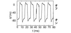
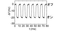
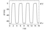
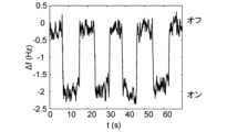
光センサ10の応答速度は1/τとなるため、τが小さければ光センサ10の応答が速くなる。光センサ10の応答速度の高速性を示すため、入力光の変調周波数を変調し、共振周波数のシフトが測定された。The response speed of the
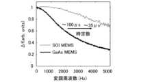
図12には、変調周波数を変化させた際の周波数シフトΔfの計測結果が示されている。図示するように、光センサ10と同サイズの従来のGaAsにより形成された光センサとを比較すると、光センサ10の熱時定数は、約35μsであったのに比して、従来のGaAsにより形成された光センサの熱時定数は、約100μsであった。この計測結果が示す通り、同じ形状の光センサ10と従来のGaAsにより形成された光センサとを比較すると、光センサ10の熱応答は、従来のGaAsにより形成された光センサの熱応答に比して約3倍の速度であることが分かる。Figure 12 shows the measurement results of the frequency shift Δf when the modulation frequency is changed. As shown in the figure, when comparing
図13に示されるように、光センサ10によれば、従来用いられてきた抵抗や静電容量の変化を利用した熱型センサに比して、同等の感度を有しつつも、検出速度(Hz)が100~1000倍であることが分かる。広帯域光検出装置1によれば、光センサ10がSOI材料により形成されたMEMS構造を備え、高抵抗であり高い光透過率を有するボロメータを低コストで実現することができる。広帯域光検出装置1によれば、光センサ10に基づいて室温において動作し、広帯域、高感度、高速、低コストである高性能のボロメータを実現することができる。As shown in Figure 13, the
光センサ10によれば、SOI基板により形成されているため、広い周波数領域で高透過率であり、可視光から、赤外線、テラヘルツ波まで計測可能であり、室温動作する・高速・高感度なセンサを実現することができる。光センサ10によれば、成長プロセスが複雑なGaAsヘテロ構造に比して安価なSOI基板構造を用いるため、MEMSボロメータを低コストで量産することができる。光センサ10によれば、一般的なシリコン半導体技術を用いるため、容易に量産化することができる。Since the
光センサ10によれば、可視光から、赤外線、テラヘルツ波までの、幅広い波長帯の光に対して高感度であるため、従来のGaAsにより同形状に形成されたMEMS光センサに比して、約3倍の検出速度を有している。光センサ10によれば、シリコン系の素材により形成されているため、成長のプロセスを簡略化すると共に、安価に形成することができる。光センサ10が適用された広帯域光検出装置1によれば、テラヘルツから赤外線領域における検出感度が低下する不感度帯が無く広帯域、高速、高感度な光検出装置、分光装置、生体イメージング装置を実現することができる。The
なお、シリコン系の素材により両持梁共振器型光センサを形成しようとすると、物理的な成膜方式で堆積された梁構造の内部応力が大きいという課題があった。しかしながら、本発明者らは、内部応力が小さい結晶性SOI材料(例えば、単結晶SOI基板)により形成されたMEMS構造を採用することによって、上記の内部応力の問題を解決できることを見出した。このように、SOI材料により形成されたMEMS両持梁構造を利用した場合、光センサの性能をさらに向上させることができる。たとえば、上記の非特許文献2に記載された例は、物理的に成膜されたa-Siを採用しているので、MEMS構造の内部応力が比較的大きい。このため、温度感度が不十分なねじれモードしか使用できない。この非特許文献2に記載された例と比較すると、上記の光センサ10の温度感度は約20倍高い。なお、非特許文献3にはSOI基板を使用する例が記載されているが、これは上記のような梁構造の内部応力を考慮したものではない。非特許文献3に記載された例は、カンチレバー構造を採用しているので、構造内部の初期応力は無関係である。また、非特許文献3には、材料の結晶性についての記載もない。さらに、非特許文献3に記載された例では、カンチレバー構造を採用しているので、温度感度は約10nW/Hz0.5であり、上記の光センサ10の方が10倍以上優れている。 In addition, when attempting to form a doubly supported beam resonator type optical sensor using silicon-based materials, there was a problem that the internal stress of the beam structure deposited by the physical film deposition method was large. However, the present inventors have found that the above-mentioned internal stress problem can be solved by adopting a MEMS structure formed from a crystalline SOI material (e.g., a single crystal SOI substrate) with small internal stress. In this way, when a MEMS doubly supported beam structure formed from an SOI material is used, the performance of the optical sensor can be further improved. For example, the example described in the above
光センサ10が適用された広帯域光検出装置1によれば、近赤外・赤外・テラヘルツ周波数帯を利用する産業分野へ応用することができる。光センサ10が適用された広帯域光検出装置1によれば、材料・化学や製薬・バイオなどの分野の必須装置であるテラヘルツ・赤外フーリエ分光器(FTIR)を実現することができる。以下、光センサ10が適用されたFTIRについて説明する。以下の説明では、上記実施形態と同一の構成については同一の名称及び符号を用い、重複する説明は適宜省略する。The broadband
図16に示されるように、FTIR100は、光センサ10を備える広帯域光検出装置1と、レンズ部Nと、光源Rと、干渉光を生成する干渉光生成部Uと、広帯域光検出装置1により検出された光を解析する演算装置40とを備えている。FTIR100は、干渉計を用いて光の干渉波形を測定し、測定値をフーリエ変換することにより光のスペクトルの強度分布を測定する分光装置に構成されている。FTIR100の使用時には、試料Sが広帯域光検出装置1にセットされ、FTIR100は、試料Sの光学的特性などを調べることができる。なお、試料Sは、図16では干渉光生成部Uの半透鏡U1とレンズ部Nとの間に配置されているが、この配置に限定されず、分光測定が可能な任意の位置に配置されてよい。レンズ部Nは、シリコンによりレンズ状に形成され、入力される光を集光し、光センサ10に入力する。演算装置40は、光センサ10に入力された光のスペクトルを解析して出力する。演算装置40は、例えば、パーソナルコンピュータ等により構成された情報処理端末装置である。As shown in FIG. 16, the
干渉光生成部Uは、例えば、マイケルソン干渉計であり、半透鏡U1と、固定鏡に形成された第1反射鏡U2と、移動自在な移動鏡に形成された第2反射鏡U3とを備えている。半透鏡U1は、光源Rから入力された光L1を斜方向に入射し、反射光の第1光L2と透過光の第2光L3の二つの光束に分割する。第1光L2は、第1反射鏡U2において反射して半透鏡U1に戻る。第2光L3は、第2反射鏡U3において反射して半透鏡U1に戻る。The interference light generating unit U is, for example, a Michelson interferometer, and includes a semi-transparent mirror U1, a first reflecting mirror U2 formed on a fixed mirror, and a second reflecting mirror U3 formed on a movable mirror. The semi-transparent mirror U1 receives light L1 input from the light source R at an oblique angle and splits it into two light beams: a first reflected light beam L2 and a second transmitted light beam L3. The first light beam L2 is reflected by the first reflecting mirror U2 and returns to the semi-transparent mirror U1. The second light beam L3 is reflected by the second reflecting mirror U3 and returns to the semi-transparent mirror U1.
半透鏡U1において第1光L2と第2光L3とが合成される。第2反射鏡U3は、光路方向に移動自在であり、第2光L3の光路長は、第1光L2の光路長に比して光路差が生じている。このため、半透鏡U1において第1光L2と第2光L3との間には位相差が生じ、半透鏡U1において干渉光L4が生じる。半透鏡U1において生じた干渉光L4は、シリコンレンズにより形成されたレンズ部Nにおいて集光され、光センサ10に入力される。光センサ10に入力された干渉光L4は、両持梁11Aを振動させ、振動検出装置20により振動が検出される。両持梁11Aは、干渉光L4に基づいて共振周波数が変化する。位相同期部30は、光センサ10の振動の周波数を検出する。位相同期部30により検出された検出値は、演算装置40に入力される。演算装置40は、位相同期部30により検出された検出値に基づいて光L1のスペクトルを解析する。演算装置40は、検出値における干渉光L4の干渉波形をフーリエ解析し、光源Rから出力された光L1のスペクトル解析を行う。演算装置40は、光L1のスペクトルを波長成分毎に出力する。The first light L2 and the second light L3 are combined in the semi-transparent mirror U1. The second reflecting mirror U3 is movable in the optical path direction, and an optical path difference occurs between the optical path length of the second light L3 and the optical path length of the first light L2. Therefore, a phase difference occurs between the first light L2 and the second light L3 in the semi-transparent mirror U1, and an interference light L4 occurs in the semi-transparent mirror U1. The interference light L4 generated in the semi-transparent mirror U1 is collected in the lens portion N formed by a silicon lens and input to the
第2反射鏡U3の移動による光の変調周波数は、光の周波数及び第2反射鏡U3の移動速度に比例しているため、FTIR100のスキャン速度は、光センサの検出速度に依存している。FTIR100の光強度変調周波数は、fm=2*f/c*vにより算出される。但し、fは光の周波数、cは光の速度、vは移動鏡の速度である。例えば、光が10μmの赤外線(周波数30THz)であり、移動鏡の速度が10mm/sである場合、光の変調周波数は2kHzである。The modulation frequency of light due to the movement of the second reflector U3 is proportional to the frequency of the light and the movement speed of the second reflector U3, so the scanning speed of FTIR100 depends on the detection speed of the optical sensor. The light intensity modulation frequency of FTIR100 is calculated by fm = 2 * f/c * v, where f is the frequency of light, c is the speed of light, and v is the speed of the moving mirror. For example, if the light is 10 μm infrared (
光センサ10が適用されたFTIR100によれば、従来のFTIRに用いられていた焦電型検出器に比して、検出速度が約100-1000倍であり、高速、高感度に光のスペクトル分布を計測することができる。FTIR100によれば、近赤外・赤外・テラヘルツ周波数帯の光のスペクトル分布を高速、高感度に解析するマルチチャンネル分光器を実現することができる。また、干渉光生成部Uは、マイケルソン干渉計の他、干渉光を生じさせるものであれば他の干渉計に置き換えられてもよい。また、FTIR100において光センサ10は、素子をアレー化してもよく、振動検出部の回路を集積化することにより、高速に近赤外・赤外・テラヘルツ波を検出可能なイメージング素子、サーモグラフィーを実現可能であり、夜間走行支援装置などに応用することができる。The
上述した演算装置40は、例えば、CPU(Central Processing Unit)などのハードウェアプロセッサがプログラム(ソフトウェア)を実行することにより実現される。これらの構成要素のうち一部または全部は、LSI(Large Scale Integration)やASIC(Application Specific Integrated Circuit)、FPGA(Field-Programmable Gate Array)、GPU(Graphics Processing Unit)などのハードウェア(回路部;circuitryを含む)によって実現されてもよいし、ソフトウェアとハードウェアの協働によって実現されてもよい。プログラムは、予め演算装置40に設けられたHDD(Hard Disk Drive)やフラッシュメモリなどの記憶装置に格納されていてもよいし、DVDやCD-ROMなどの着脱可能な記憶媒体に格納されており、記憶媒体がドライブ装置に装着されることでインストールされてもよい。The above-mentioned
以上、本発明を実施するための形態について実施形態を用いて説明したが、本発明はこうした実施形態に何等限定されるものではなく、本発明の要旨を逸脱しない範囲内において種々の変形及び置換を加えることができる。上記実施形態において記載された各構成は、相互に置換されてもよい。Although the above describes the form for carrying out the present invention using the embodiments, the present invention is not limited to these embodiments, and various modifications and substitutions can be made within the scope of the gist of the present invention. The configurations described in the above embodiments may be mutually substituted.
10 光センサ
11 振動部
11A 両持梁
15 吸光部
16 振動入力部
17 振動検出部
20 振動検出装置
30 位相同期部
36 振動発生部
40 演算装置
L 入力光
L1 光
R 光源10
Claims (13)
Translated fromJapaneseシリコン素材を用いたMEMS構造により形成され、前記振動入力部により伝達された振動に基づいて振動し、光が入力されることにより共振周波数が変化する両持梁を有する振動部と、
前記両持梁の振動を検出する振動検出部と、を備え、
前記MEMS構造は、高抵抗のSOI(Silicon on Insulator)基板(フォノニック結晶を除く)により形成されている、
光センサ。 a vibration input unit that generates vibrations based on an input signal;
a vibration section having a doubly supported beam formed by a MEMS structure using a silicon material, vibrating based on the vibration transmitted by the vibration input section and having a resonant frequency that changes when light is input;
a vibration detection unit that detects vibration of the double-supported beam,
The MEMS structure is formed of a high-resistance SOI (Silicon on Insulator) substrate (excluding the phononic crystal);
Light sensor.
請求項1に記載の光センサ。 The MEMS structure is formed of an SOI substrate having a flat surface.
The optical sensor of claim 1 .
請求項1または2に記載の光センサ。 The double-supported beam is provided between the vibration input unit and the vibration detection unit, and has a light absorbing unit to which temperature is transferred by inputting light.
3. The optical sensor according to claim 1 or 2.
請求項3に記載の光センサ。 The vibration input portion is formed by a piezoelectric element provided on one end side of the double-supported beam in the longitudinal direction.
The optical sensor according to claim 3 .
請求項3に記載の光センサ。 The vibration input portion is formed by an electrostatic element provided on one end side of the double-supported beam in the longitudinal direction.
The optical sensor according to claim 3 .
請求項3に記載の光センサ。 The vibration detection unit is formed of a piezoelectric element provided on the other end side of the double-supported beam in the longitudinal direction.
The optical sensor according to claim 3 .
請求項3に記載の光センサ。 The vibration detection unit is formed of a piezoresistance element provided on the other end side of the double-supported beam in the longitudinal direction.
The optical sensor according to claim 3 .
平板状に形成された基板部と、
前記基板部上に形成された一対の犠牲層と、
シリコン素材により形成され、前記一対の犠牲層を架設するように平板状に形成された前記両持梁を有する前記振動部と、を備える、
請求項3に記載の光センサ。 The MEMS structure includes:
A substrate portion formed in a flat plate shape;
A pair of sacrificial layers formed on the substrate portion;
The vibration unit is made of a silicon material and has the two-sided beam formed in a flat plate shape so as to bridge the pair of sacrificial layers.
The optical sensor according to claim 3 .
前記光センサの振動を増幅して出力する振動検出装置と、
前記振動検出装置の出力値に基づいて前記光センサの振動の周波数を検出する位相同期部と、を備え、
前記MEMS構造は、高抵抗のSOI基板(フォノニック結晶を除く)により形成されている、
光検出装置。 an optical sensor including a vibration input unit that generates vibrations based on an input signal, a vibration unit formed of a MEMS structure using a silicon material, that vibrates based on the vibration transmitted by the vibration input unit, and that has a double-supported beam whose resonance frequency changes when light is input, and a vibration detection unit that detects the vibration of the double-supported beam;
a vibration detection device that amplifies and outputs the vibration of the optical sensor;
a phase synchronization unit that detects a frequency of vibration of the optical sensor based on an output value of the vibration detection device,
The MEMS structure is formed of a high-resistance SOI substrate (excluding phononic crystals);
Light detection device.
請求項9に記載の光検出装置。 The MEMS structure is formed of an SOI substrate having a flat surface.
10. The optical detection device according to claim 9.
前記光センサに入力光を入力する光源と、
前記光センサの振動を増幅して出力する振動検出装置と、
前記振動検出装置の出力値に基づいて前記光センサの振動の周波数を検出する位相同期部と、
前記位相同期部により検出された検出値に基づいて前記光のスペクトルを解析する演算装置と、を備え、
前記MEMS構造は、高抵抗のSOI基板(フォノニック結晶を除く)により形成されている、
テラヘルツ・赤外フーリエ分光器。 an optical sensor including a vibration input unit that generates vibrations based on an input signal, a vibration unit formed of a MEMS structure using a silicon material, that vibrates based on the vibration transmitted by the vibration input unit, and that has a double-supported beam whose resonance frequency changes when light is input, a light absorption unit that transmits temperature to the double-supported beam when light is input, and a vibration detection unit that detects the vibration of the double-supported beam;
A light source that inputs input light to the optical sensor;
a vibration detection device that amplifies and outputs the vibration of the optical sensor;
a phase synchronization unit that detects a frequency of vibration of the optical sensor based on an output value of the vibration detection device;
a calculation unit that analyzes the spectrum of the light based on the detection value detected by the phase synchronization unit,
The MEMS structure is formed of a high-resistance SOI substrate (excluding phononic crystals);
Terahertz and infrared Fourier spectrometer.
請求項11に記載のテラヘルツ・赤外フーリエ分光器。 The MEMS structure is formed of an SOI substrate having a flat surface.
The terahertz/infrared Fourier spectrometer according to claim 11.
請求項1に記載の光センサ。 The resistivity of the SOI substrate is greater than 1000 Ω cm;
The optical sensor of claim 1 .
Applications Claiming Priority (3)
| Application Number | Priority Date | Filing Date | Title |
|---|---|---|---|
| JP2022087832 | 2022-05-30 | ||
| JP2022087832 | 2022-05-30 | ||
| PCT/JP2023/016930WO2023233900A1 (en) | 2022-05-30 | 2023-04-28 | Light sensor, light detection device, and terahertz/infrared fourier spectroscope |
Publications (3)
| Publication Number | Publication Date |
|---|---|
| JPWO2023233900A1 JPWO2023233900A1 (en) | 2023-12-07 |
| JPWO2023233900A5 JPWO2023233900A5 (en) | 2024-12-13 |
| JP7619708B2true JP7619708B2 (en) | 2025-01-22 |
Family
ID=89026380
Family Applications (1)
| Application Number | Title | Priority Date | Filing Date |
|---|---|---|---|
| JP2024524256AActiveJP7619708B2 (en) | 2022-05-30 | 2023-04-28 | Optical sensor, optical detection device, and terahertz/infrared Fourier spectrometer |
Country Status (4)
| Country | Link |
|---|---|
| EP (1) | EP4517281A4 (en) |
| JP (1) | JP7619708B2 (en) |
| CN (1) | CN119422038A (en) |
| WO (1) | WO2023233900A1 (en) |
Citations (5)
| Publication number | Priority date | Publication date | Assignee | Title |
|---|---|---|---|---|
| JP2007527508A (en) | 2003-07-03 | 2007-09-27 | キネティック リミテッド | Thermal device |
| US20140353506A1 (en) | 2012-10-09 | 2014-12-04 | Samsung Electronics Co., Ltd. | Electromagnetic wave spectrum analyzer and infrared thermal image analyzer including multiple resonance structures each having different resonance frequency |
| US20160065169A1 (en) | 2013-04-22 | 2016-03-03 | Northeastern University | Nano- and micro-electromechanical resonators |
| JP2018146294A (en) | 2017-03-02 | 2018-09-20 | 国立大学法人 東京大学 | Terahertz wave detection device |
| CN112710402A (en) | 2020-12-22 | 2021-04-27 | 武汉大学 | Resonant thermal infrared sensor and preparation method thereof |
Family Cites Families (5)
| Publication number | Priority date | Publication date | Assignee | Title |
|---|---|---|---|---|
| JPH0783756A (en)* | 1993-09-10 | 1995-03-31 | Semiconductor Res Found | Oscillatory type infrared sensor, oscillatory type infrared imager, and infrared-ray detecting method |
| JPH10281862A (en)* | 1997-04-08 | 1998-10-23 | Yokogawa Electric Corp | Vibration type infrared sensor and manufacturing method thereof |
| CN101063630A (en)* | 2007-06-01 | 2007-10-31 | 中国计量学院 | Infrared detector structure based on micro-bridge resonator and manufacturing method |
| EP2141490B1 (en)* | 2008-07-02 | 2015-04-01 | Stichting IMEC Nederland | Chemical sensing microbeam device |
| JP2022087832A (en) | 2020-12-01 | 2022-06-13 | Cs計時株式会社 | Colored timekeeping device |
- 2023
- 2023-04-28CNCN202380043457.8Apatent/CN119422038A/enactivePending
- 2023-04-28JPJP2024524256Apatent/JP7619708B2/enactiveActive
- 2023-04-28EPEP23815661.6Apatent/EP4517281A4/enactivePending
- 2023-04-28WOPCT/JP2023/016930patent/WO2023233900A1/ennot_activeCeased
Patent Citations (5)
| Publication number | Priority date | Publication date | Assignee | Title |
|---|---|---|---|---|
| JP2007527508A (en) | 2003-07-03 | 2007-09-27 | キネティック リミテッド | Thermal device |
| US20140353506A1 (en) | 2012-10-09 | 2014-12-04 | Samsung Electronics Co., Ltd. | Electromagnetic wave spectrum analyzer and infrared thermal image analyzer including multiple resonance structures each having different resonance frequency |
| US20160065169A1 (en) | 2013-04-22 | 2016-03-03 | Northeastern University | Nano- and micro-electromechanical resonators |
| JP2018146294A (en) | 2017-03-02 | 2018-09-20 | 国立大学法人 東京大学 | Terahertz wave detection device |
| CN112710402A (en) | 2020-12-22 | 2021-04-27 | 武汉大学 | Resonant thermal infrared sensor and preparation method thereof |
Also Published As
| Publication number | Publication date |
|---|---|
| JPWO2023233900A1 (en) | 2023-12-07 |
| WO2023233900A1 (en) | 2023-12-07 |
| EP4517281A1 (en) | 2025-03-05 |
| CN119422038A (en) | 2025-02-11 |
| EP4517281A4 (en) | 2025-09-17 |
Similar Documents
| Publication | Publication Date | Title |
|---|---|---|
| US11099076B2 (en) | Graphene nanomechanical radiation detector | |
| US10520365B2 (en) | Detector for terahertz electromagnetic waves | |
| Pisani et al. | Application of micromachined $ Y $-cut-Quartz bulk acoustic wave resonator for infrared sensing | |
| Vicarelli et al. | Micromechanical bolometers for subterahertz detection at room temperature | |
| Hui et al. | Plasmonic piezoelectric nanomechanical resonator for spectrally selective infrared sensing | |
| Piller et al. | Thermal IR detection with nanoelectromechanical silicon nitride trampoline resonators | |
| Hui et al. | High performance NEMS resonant infrared detector based on an aluminum nitride nano-plate resonator | |
| ES2966309T3 (en) | Photoacoustic spectroscope with vibrating structure as a sound detector | |
| Kao et al. | Micromachined quartz resonator based infrared detector array | |
| JP2013540264A (en) | Bolometer for frequency detection | |
| Wang et al. | ZnO based film bulk acoustic resonator as infrared sensor | |
| CN109245741A (en) | A kind of infrared detector | |
| Chamassi et al. | Capacitive silicon micro-electromechanical resonator for enhanced photoacoustic spectroscopy | |
| Chen et al. | Dual-mode resonant infrared detector based on film bulk acoustic resonator toward ultra-high sensitivity and anti-interference capability | |
| Qian et al. | High figure-of-merit NEMS thermal detectors based on 50-nm thick AlN nano-plate resonators | |
| US20150253196A1 (en) | Uncooled ir detector arrays based on nanoelectromechanical systems | |
| JP7619708B2 (en) | Optical sensor, optical detection device, and terahertz/infrared Fourier spectrometer | |
| Martini et al. | Uncooled thermal infrared detection near the fundamental limit using a silicon nitride nanomechanical resonator with a broadband absorber | |
| CN109358373A (en) | Detector and its control method | |
| Ayed et al. | Advancing infrared sensing with high-tcf 30%-doped scaln resonators and aln metamaterial absorbers | |
| Suzuki et al. | Short-wavelength infrared light sensing using an electrostatic MEMS resonator integrated with a plasmonic optical absorber | |
| Quan et al. | Dual-Mode Thermal-Piezoresistive Coupled Resonators for Fast and Stable NIR Measurements with Differential Output | |
| Zhang et al. | Uncooled, broadband terahertz bolometers using SOI MEMS beam resonators with piezoresistive readout | |
| Li et al. | Cmos-mems resonant transducers for frequency control and sensing | |
| Hui et al. | MEMS resonant infrared sensors |
Legal Events
| Date | Code | Title | Description |
|---|---|---|---|
| A529 | Written submission of copy of amendment under article 34 pct | Free format text:JAPANESE INTERMEDIATE CODE: A5211 Effective date:20241016 | |
| A621 | Written request for application examination | Free format text:JAPANESE INTERMEDIATE CODE: A621 Effective date:20241016 | |
| A871 | Explanation of circumstances concerning accelerated examination | Free format text:JAPANESE INTERMEDIATE CODE: A871 Effective date:20241016 | |
| A521 | Request for written amendment filed | Free format text:JAPANESE INTERMEDIATE CODE: A821 Effective date:20241016 | |
| TRDD | Decision of grant or rejection written | ||
| A01 | Written decision to grant a patent or to grant a registration (utility model) | Free format text:JAPANESE INTERMEDIATE CODE: A01 Effective date:20241217 | |
| A61 | First payment of annual fees (during grant procedure) | Free format text:JAPANESE INTERMEDIATE CODE: A61 Effective date:20241226 | |
| R150 | Certificate of patent or registration of utility model | Ref document number:7619708 Country of ref document:JP Free format text:JAPANESE INTERMEDIATE CODE: R150 |