JP7618566B2 - Electronics - Google Patents
ElectronicsDownload PDFInfo
- Publication number
- JP7618566B2 JP7618566B2JP2021547978AJP2021547978AJP7618566B2JP 7618566 B2JP7618566 B2JP 7618566B2JP 2021547978 AJP2021547978 AJP 2021547978AJP 2021547978 AJP2021547978 AJP 2021547978AJP 7618566 B2JP7618566 B2JP 7618566B2
- Authority
- JP
- Japan
- Prior art keywords
- light
- layer
- emitting element
- function
- receiving element
- Prior art date
- Legal status (The legal status is an assumption and is not a legal conclusion. Google has not performed a legal analysis and makes no representation as to the accuracy of the status listed.)
- Active
Links
Images


Classifications
- G—PHYSICS
- G06—COMPUTING OR CALCULATING; COUNTING
- G06F—ELECTRIC DIGITAL DATA PROCESSING
- G06F3/00—Input arrangements for transferring data to be processed into a form capable of being handled by the computer; Output arrangements for transferring data from processing unit to output unit, e.g. interface arrangements
- G06F3/01—Input arrangements or combined input and output arrangements for interaction between user and computer
- G06F3/03—Arrangements for converting the position or the displacement of a member into a coded form
- G06F3/041—Digitisers, e.g. for touch screens or touch pads, characterised by the transducing means
- G06F3/0412—Digitisers structurally integrated in a display
- G—PHYSICS
- G06—COMPUTING OR CALCULATING; COUNTING
- G06F—ELECTRIC DIGITAL DATA PROCESSING
- G06F3/00—Input arrangements for transferring data to be processed into a form capable of being handled by the computer; Output arrangements for transferring data from processing unit to output unit, e.g. interface arrangements
- G06F3/01—Input arrangements or combined input and output arrangements for interaction between user and computer
- G06F3/03—Arrangements for converting the position or the displacement of a member into a coded form
- G06F3/041—Digitisers, e.g. for touch screens or touch pads, characterised by the transducing means
- G06F3/042—Digitisers, e.g. for touch screens or touch pads, characterised by the transducing means by opto-electronic means
- G—PHYSICS
- G06—COMPUTING OR CALCULATING; COUNTING
- G06V—IMAGE OR VIDEO RECOGNITION OR UNDERSTANDING
- G06V40/00—Recognition of biometric, human-related or animal-related patterns in image or video data
- G06V40/10—Human or animal bodies, e.g. vehicle occupants or pedestrians; Body parts, e.g. hands
- G06V40/12—Fingerprints or palmprints
- G06V40/13—Sensors therefor
- G06V40/1318—Sensors therefor using electro-optical elements or layers, e.g. electroluminescent sensing
- G—PHYSICS
- G06—COMPUTING OR CALCULATING; COUNTING
- G06V—IMAGE OR VIDEO RECOGNITION OR UNDERSTANDING
- G06V40/00—Recognition of biometric, human-related or animal-related patterns in image or video data
- G06V40/10—Human or animal bodies, e.g. vehicle occupants or pedestrians; Body parts, e.g. hands
- G06V40/12—Fingerprints or palmprints
- G06V40/1365—Matching; Classification
- G—PHYSICS
- G06—COMPUTING OR CALCULATING; COUNTING
- G06V—IMAGE OR VIDEO RECOGNITION OR UNDERSTANDING
- G06V40/00—Recognition of biometric, human-related or animal-related patterns in image or video data
- G06V40/50—Maintenance of biometric data or enrolment thereof
- H—ELECTRICITY
- H10—SEMICONDUCTOR DEVICES; ELECTRIC SOLID-STATE DEVICES NOT OTHERWISE PROVIDED FOR
- H10K—ORGANIC ELECTRIC SOLID-STATE DEVICES
- H10K50/00—Organic light-emitting devices
- H10K50/80—Constructional details
- H10K50/805—Electrodes
- H10K50/81—Anodes
- H10K50/813—Anodes characterised by their shape
- H—ELECTRICITY
- H10—SEMICONDUCTOR DEVICES; ELECTRIC SOLID-STATE DEVICES NOT OTHERWISE PROVIDED FOR
- H10K—ORGANIC ELECTRIC SOLID-STATE DEVICES
- H10K50/00—Organic light-emitting devices
- H10K50/80—Constructional details
- H10K50/805—Electrodes
- H10K50/82—Cathodes
- H10K50/822—Cathodes characterised by their shape
- H—ELECTRICITY
- H10—SEMICONDUCTOR DEVICES; ELECTRIC SOLID-STATE DEVICES NOT OTHERWISE PROVIDED FOR
- H10K—ORGANIC ELECTRIC SOLID-STATE DEVICES
- H10K59/00—Integrated devices, or assemblies of multiple devices, comprising at least one organic light-emitting element covered by group H10K50/00
- H10K59/60—OLEDs integrated with inorganic light-sensitive elements, e.g. with inorganic solar cells or inorganic photodiodes
- H—ELECTRICITY
- H10—SEMICONDUCTOR DEVICES; ELECTRIC SOLID-STATE DEVICES NOT OTHERWISE PROVIDED FOR
- H10K—ORGANIC ELECTRIC SOLID-STATE DEVICES
- H10K65/00—Integrated devices, or assemblies of multiple devices, comprising at least one organic light-emitting element and at least one organic radiation-sensitive element, e.g. organic opto-couplers
- G—PHYSICS
- G06—COMPUTING OR CALCULATING; COUNTING
- G06F—ELECTRIC DIGITAL DATA PROCESSING
- G06F2203/00—Indexing scheme relating to G06F3/00 - G06F3/048
- G06F2203/041—Indexing scheme relating to G06F3/041 - G06F3/045
- G06F2203/04103—Manufacturing, i.e. details related to manufacturing processes specially suited for touch sensitive devices
- G—PHYSICS
- G06—COMPUTING OR CALCULATING; COUNTING
- G06F—ELECTRIC DIGITAL DATA PROCESSING
- G06F2203/00—Indexing scheme relating to G06F3/00 - G06F3/048
- G06F2203/041—Indexing scheme relating to G06F3/041 - G06F3/045
- G06F2203/04111—Cross over in capacitive digitiser, i.e. details of structures for connecting electrodes of the sensing pattern where the connections cross each other, e.g. bridge structures comprising an insulating layer, or vias through substrate
- H—ELECTRICITY
- H10—SEMICONDUCTOR DEVICES; ELECTRIC SOLID-STATE DEVICES NOT OTHERWISE PROVIDED FOR
- H10K—ORGANIC ELECTRIC SOLID-STATE DEVICES
- H10K59/00—Integrated devices, or assemblies of multiple devices, comprising at least one organic light-emitting element covered by group H10K50/00
- H10K59/30—Devices specially adapted for multicolour light emission
- H10K59/35—Devices specially adapted for multicolour light emission comprising red-green-blue [RGB] subpixels
- H10K59/353—Devices specially adapted for multicolour light emission comprising red-green-blue [RGB] subpixels characterised by the geometrical arrangement of the RGB subpixels
Landscapes
- Engineering & Computer Science (AREA)
- Theoretical Computer Science (AREA)
- Physics & Mathematics (AREA)
- Human Computer Interaction (AREA)
- General Physics & Mathematics (AREA)
- General Engineering & Computer Science (AREA)
- Multimedia (AREA)
- Optics & Photonics (AREA)
- Life Sciences & Earth Sciences (AREA)
- Chemical & Material Sciences (AREA)
- Inorganic Chemistry (AREA)
- Sustainable Development (AREA)
- Image Input (AREA)
- Position Input By Displaying (AREA)
Description
Translated fromJapanese本発明の一態様は、電子機器に関する。本発明の一態様は、表示装置に関する。本発明の一態様は、プログラムに関する。1. Field of the Invention The present invention relates to an electronic device, a display device, and a program.
なお、本発明の一態様は、上記の技術分野に限定されない。本発明の一態様の技術分野としては、半導体装置、表示装置、発光装置、蓄電装置、記憶装置、電子機器、照明装置、入力装置(例えば、タッチセンサなど)、入出力装置(例えば、タッチパネルなど)、それらの駆動方法、又はそれらの製造方法を一例として挙げることができる。Note that one embodiment of the present invention is not limited to the above technical field. Examples of the technical field of one embodiment of the present invention include a semiconductor device, a display device, a light-emitting device, a power storage device, a memory device, an electronic device, a lighting device, an input device (e.g., a touch sensor), an input/output device (e.g., a touch panel), a driving method thereof, or a manufacturing method thereof.
近年、スマートフォンなどの携帯電話、タブレット型情報端末などの情報端末機器の多くは簡単な操作で様々な処理を実行する機能が搭載されている。例えば、操作のバリエーションを増やすために、タッチの強さ(圧力)を検出し、圧力の度合いによって実行する処理を変える機能などがある。In recent years, many information terminal devices, such as mobile phones such as smartphones and tablet information terminals, are equipped with functions that can execute various processes with simple operations. For example, in order to increase the variety of operations, there are functions that detect the strength (pressure) of a touch and change the process to be executed depending on the degree of pressure.
また、このような情報端末機器は、個人情報などが含まれることが多く、不正な利用を防止するための様々な認証技術が開発されている。Furthermore, such information terminal devices often contain personal information, and various authentication techniques have been developed to prevent unauthorized use.
例えば、特許文献1には、プッシュボタンスイッチ部に、指紋センサを備える電子機器が開示されている。For example, Patent Document 1 discloses an electronic device that includes a fingerprint sensor in a push button switch section.
情報端末機器で広く用いられている静電容量式のタッチセンサは、ディスプレイ表面の静電容量の変化を利用して接触の感知を行う。静電容量式のタッチセンサでは指や静電式のタッチペン等の位置を判断することは可能でも、ディスプレイに加えられる圧力を検出することはできない。そのためタッチの仕方の違いを検出するのに、押し込みを感知可能な感圧センサを搭載しているものが多い。しかし、感圧センサを内蔵することで情報端末機器の部品点数が増えてしまう。Capacitive touch sensors, which are widely used in information terminal devices, detect touch by utilizing changes in the capacitance of the display surface. Although capacitive touch sensors can determine the position of a finger or electrostatic touch pen, they cannot detect the pressure applied to the display. For this reason, many capacitive touch sensors are equipped with pressure sensors that can detect pressure to detect differences in touch methods. However, incorporating a pressure sensor increases the number of parts in an information terminal device.
本発明の一態様は、タッチの仕方の違いを検出することが可能な電子機器を提供することを課題の一とする。または、本発明の一態様は、少ない部品点数で、かつ、タッチの仕方の違いを検出することが可能な電子機器を提供することを課題の一とする。または、本発明の一様態は、簡単な操作で様々な処理を実行することができる電子機器を提供することを課題の一とする。または、本発明の一態様は、新規な電子機器を提供することを課題の一とする。An object of one embodiment of the present invention is to provide an electronic device that can detect differences in touching methods.Another object of one embodiment of the present invention is to provide an electronic device that can detect differences in touching methods with a small number of components.Another object of one embodiment of the present invention is to provide an electronic device that can execute various processes with a simple operation.Another object of one embodiment of the present invention is to provide a novel electronic device.
なお、これらの課題の記載は、他の課題の存在を妨げるものではない。本発明の一態様は、必ずしも、これらの課題の全てを解決する必要はないものとする。明細書、図面、請求項の記載から、これら以外の課題を抽出することが可能である。Note that the description of these problems does not preclude the existence of other problems. One embodiment of the present invention does not necessarily have to solve all of these problems. Problems other than these can be extracted from the description of the specification, drawings, and claims.
本発明の一態様は、制御部と、表示部と、を有する電子機器である。表示部は、画面に画像を表示する機能を有し、かつ、検出部を有する。検出部は、タッチ操作を検出する機能と、画面に触れた被検出体を少なくとも2回撮像する機能と、を有する。制御部は、1回目の撮像における被検出体の面積と2回目の撮像における被検出体の面積との差を算出して、当該差が基準よりも大きい場合と小さい場合で異なる処理を実行する機能を有する。One aspect of the present invention is an electronic device having a control unit and a display unit. The display unit has a function of displaying an image on a screen and has a detection unit. The detection unit has a function of detecting a touch operation and a function of capturing an image of a detectable object touching the screen at least twice. The control unit has a function of calculating a difference between an area of the detectable object captured in a first image and an area of the detectable object captured in a second image, and executing different processes depending on whether the difference is larger or smaller than a reference value.
また、本発明の他の一態様は、制御部と、表示部と、記憶部と、を有する電子機器である。表示部は、画面に画像を表示する機能を有し、かつ、検出部を有する。検出部は、タッチ操作を検出する機能と、画面に触れた被検出体を撮像する機能と、を有する。制御部は、検出部が撮像したデータから、被検出体の接触面積の情報を取得する機能を有する。記憶部は、あらかじめ登録された基準の接触面積の情報を保持する機能を有する。制御部は、被検出体の接触面積が、基準の接触面積よりも大きい場合と小さい場合で異なる処理を実行する機能を有する。Another aspect of the present invention is an electronic device having a control unit, a display unit, and a memory unit. The display unit has a function of displaying an image on a screen, and has a detection unit. The detection unit has a function of detecting a touch operation and a function of capturing an image of a detectable object touching the screen. The control unit has a function of acquiring information on the contact area of the detectable object from data captured by the detection unit. The memory unit has a function of retaining information on a reference contact area registered in advance. The control unit has a function of executing different processes depending on whether the contact area of the detectable object is larger or smaller than the reference contact area.
また、本発明の他の一態様は、制御部と、表示部と、記憶部と、を有する電子機器である。表示部は、画面に画像を表示する機能を有し、かつ、検出部を有する。検出部は、画面へのタッチ操作を検出する機能と、画面に触れた指を撮像する機能と、を有する。制御部は、検出部が撮像したデータから、指の接触面積の情報と、指の指紋情報と、を取得する機能を有する。記憶部は、それぞれあらかじめ登録された、照合用の指紋情報と、基準の接触面積の情報と、を保持する機能を有する。制御部は、指の指紋情報と照合用の指紋情報を照合する機能と、指の指紋情報と、照合用の指紋情報が一致した場合に、指の接触面積が、基準の接触面積よりも大きい場合と小さい場合で異なる処理を実行する機能と、を有する。Another aspect of the present invention is an electronic device having a control unit, a display unit, and a storage unit. The display unit has a function of displaying an image on a screen, and also has a detection unit. The detection unit has a function of detecting a touch operation on the screen, and a function of capturing an image of a finger touching the screen. The control unit has a function of acquiring information on a contact area of the finger and fingerprint information of the finger from data captured by the detection unit. The storage unit has a function of retaining fingerprint information for matching and information on a reference contact area, each of which is registered in advance. The control unit has a function of matching the fingerprint information of the finger with the fingerprint information for matching, and a function of executing different processes depending on whether the contact area of the finger is larger or smaller than the reference contact area when the fingerprint information of the finger matches the fingerprint information for matching.
また、上記において、表示部は、複数の画素と、表示領域全体を用いて撮像する機能を有することが好ましい。このとき、画素は、発光素子と、受光素子と、を有し、発光素子と、受光素子とは、同一面上に設けられることが好ましい。In the above, it is preferable that the display unit has a function of capturing an image using a plurality of pixels and an entire display area. In this case, it is preferable that the pixel has a light-emitting element and a light-receiving element, and the light-emitting element and the light-receiving element are provided on the same surface.
また、上記において、発光素子は、第1の電極と、発光層と、共通電極と、が積層された積層構造を有することが好ましい。また受光素子は、第2の電極と、活性層と、共通電極と、が積層された積層構造を有することが好ましい。このとき、発光層と、活性層とは、それぞれ互いに異なる有機化合物を含むことが好ましい。また、第1の電極と、第2の電極とは、同一面上に離間して設けられ、共通電極は、発光層及び活性層を覆って設けられることが好ましい。In the above, the light-emitting element preferably has a laminated structure in which a first electrode, a light-emitting layer, and a common electrode are laminated. The light-receiving element preferably has a laminated structure in which a second electrode, an active layer, and a common electrode are laminated. In this case, it is preferable that the light-emitting layer and the active layer each contain different organic compounds. It is also preferable that the first electrode and the second electrode are provided on the same plane and spaced apart from each other, and the common electrode is provided to cover the light-emitting layer and the active layer.
または、上記において、発光素子は、第1の電極と、共通層と、発光層と、共通電極と、が積層された積層構造を有することが好ましい。また受光素子は、第2の電極と、共通層と、活性層と、共通電極と、が積層された積層構造を有することが好ましい。このとき、発光層と、活性層とは、それぞれ互いに異なる有機化合物を含むことが好ましい。また第1の電極と、第2の電極とは、同一面上に離間して設けられ、共通電極は、発光層及び活性層を覆って設けられ、共通層は、第1の電極及び第2の電極を覆って設けられることが好ましい。Alternatively, in the above, the light-emitting element preferably has a laminated structure in which a first electrode, a common layer, a light-emitting layer, and a common electrode are laminated. Also, the light-receiving element preferably has a laminated structure in which a second electrode, a common layer, an active layer, and a common electrode are laminated. In this case, it is preferable that the light-emitting layer and the active layer each contain different organic compounds. Also, it is preferable that the first electrode and the second electrode are provided on the same surface and spaced apart from each other, the common electrode is provided to cover the light-emitting layer and the active layer, and the common layer is provided to cover the first electrode and the second electrode.
また、上記において、発光素子は、可視光を発する機能を有し、受光素子は、発光素子が発する可視光を受光する機能を有することが好ましい。In the above, it is preferable that the light-emitting element has a function of emitting visible light, and the light-receiving element has a function of receiving the visible light emitted by the light-emitting element.
または、上記において、発光素子は、赤外光を発する機能を有し、受光素子は、発光素子が発する赤外光を受光する機能を有することが好ましい。Alternatively, in the above, it is preferable that the light-emitting element has a function of emitting infrared light, and the light-receiving element has a function of receiving the infrared light emitted by the light-emitting element.
本発明の一態様により、タッチの仕方の違いを検出することが可能な電子機器を提供することができる。または、本発明の一態様により、少ない部品点数で、かつ、タッチの仕方の違いを検出することが可能な電子機器を提供することができる。または、本発明の一様態により、簡単な操作で様々な処理を実行することができる電子機器を提供することができる。または、本発明の一態様により、新規な電子機器を提供することができる。According to one embodiment of the present invention, an electronic device capable of detecting differences in touching manners can be provided. According to one embodiment of the present invention, an electronic device capable of detecting differences in touching manners with a small number of components can be provided. According to one embodiment of the present invention, an electronic device capable of executing various processes with a simple operation can be provided. According to one embodiment of the present invention, a novel electronic device can be provided.
なお、これらの効果の記載は、他の効果の存在を妨げるものではない。本発明の一態様は、必ずしも、これらの効果の全てを有する必要はない。明細書、図面、請求項の記載から、これら以外の効果を抽出することが可能である。Note that the description of these effects does not preclude the existence of other effects. One embodiment of the present invention does not necessarily have all of these effects. Effects other than these can be extracted from the description in the specification, drawings, and claims.
図1は、デバイスの構成例を説明する図である。
図2は、デバイスの動作方法例を説明する図である。
図3は、デバイスの動作方法例を説明する図である。
図4A及び図4Bは、指を撮像している様子とその撮像データを示す図である。
図5A及び図5Bは、時間経過により変化する指の接触面積を示す図である。
図6A~図6D、図6Fは、表示装置の一例を示す断面図である。図6E、図6Gは、表示装置が撮像した画像の例を示す図である。図6H、図6J~図6Lは、画素の一例を示す上面図である。
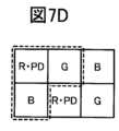
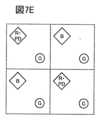
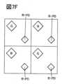
図7A~図7Gは、画素の一例を示す上面図である。
図8A、図8Bは、表示装置の一例を示す断面図である。
図9A、図9Bは、表示装置の一例を示す断面図である。
図10A~図10Cは、表示装置の一例を示す断面図である。
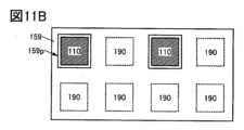
図11Aは、表示装置の一例を示す断面図である。図11B、図11Cは、樹脂層の上面レイアウトの一例を示す図である。
図12は、表示装置の一例を示す斜視図である。
図13は、表示装置の一例を示す断面図である。
図14は、表示装置の一例を示す断面図である。
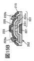
図15Aは、表示装置の一例を示す断面図である。図15Bは、トランジスタの一例を示す断面図である。
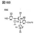
図16A、図16Bは、画素回路の一例を示す回路図である。
図17A、図17Bは、電子機器の一例を示す図である。
図18A~図18Dは、電子機器の一例を示す図である。
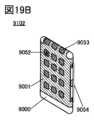
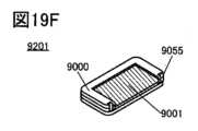
図19A~図19Fは、電子機器の一例を示す図である。FIG. 1 is a diagram illustrating an example of the configuration of a device.
FIG. 2 is a diagram illustrating an example method of operation of the device.
FIG. 3 is a diagram illustrating an example method of operation of the device.
4A and 4B are diagrams showing the state in which an image of a finger is being captured and the captured image data.
5A and 5B are diagrams showing the change in the contact area of a finger over time.
6A to 6D and 6F are cross-sectional views showing an example of a display device. Fig. 6E and Fig. 6G are diagrams showing examples of images captured by the display device. Fig. 6H and Fig. 6J to Fig. 6L are top views showing examples of pixels.
7A to 7G are top views showing an example of a pixel.
8A and 8B are cross-sectional views showing an example of a display device.
9A and 9B are cross-sectional views showing an example of a display device.
10A to 10C are cross-sectional views showing an example of a display device.
Fig. 11A is a cross-sectional view showing an example of a display device, and Fig. 11B and Fig. 11C are diagrams showing an example of a top surface layout of a resin layer.
FIG. 12 is a perspective view showing an example of a display device.
FIG. 13 is a cross-sectional view showing an example of a display device.
FIG. 14 is a cross-sectional view showing an example of a display device.
15A is a cross-sectional view illustrating an example of a display device, and FIG 15B is a cross-sectional view illustrating an example of a transistor.
16A and 16B are circuit diagrams showing an example of a pixel circuit.
17A and 17B are diagrams showing an example of an electronic device.
18A to 18D are diagrams showing an example of an electronic device.
19A to 19F are diagrams showing an example of an electronic device.
実施の形態について、図面を用いて詳細に説明する。但し、本発明は以下の説明に限定されず、本発明の趣旨及びその範囲から逸脱することなくその形態及び詳細を様々に変更し得ることは当業者であれば容易に理解される。従って、本発明は以下に示す実施の形態の記載内容に限定して解釈されるものではない。The embodiments will be described in detail with reference to the drawings. However, the present invention is not limited to the following description, and it will be easily understood by those skilled in the art that the modes and details of the present invention can be modified in various ways without departing from the spirit and scope of the present invention. Therefore, the present invention should not be interpreted as being limited to the description of the embodiments shown below.
なお、以下に説明する発明の構成において、同一部分又は同様な機能を有する部分には同一の符号を異なる図面間で共通して用い、その繰り返しの説明は省略する。また、同様の機能を指す場合には、ハッチパターンを同じくし、特に符号を付さない場合がある。In the configuration of the invention described below, the same parts or parts having similar functions are denoted by the same reference numerals in different drawings, and the repeated explanations are omitted. In addition, when referring to similar functions, the same hatch pattern may be used and no particular reference numeral may be used.
また、図面において示す各構成の、位置、大きさ、範囲などは、理解の簡単のため、実際の位置、大きさ、範囲などを表していない場合がある。このため、開示する発明は、必ずしも、図面に開示された位置、大きさ、範囲などに限定されない。In addition, for ease of understanding, the position, size, range, etc. of each component shown in the drawings may not represent the actual position, size, range, etc. Therefore, the disclosed invention is not necessarily limited to the position, size, range, etc. disclosed in the drawings.
なお、「膜」という言葉と、「層」という言葉とは、場合によっては、又は、状況に応じて、互いに入れ替えることが可能である。例えば、「導電層」という用語を、「導電膜」という用語に変更することが可能である。または、例えば、「絶縁膜」という用語を、「絶縁層」という用語に変更することが可能である。In addition, the words "film" and "layer" can be interchanged depending on the case or situation. For example, the term "conductive layer" can be changed to the term "conductive film". Or, for example, the term "insulating film" can be changed to the term "insulating layer".
(実施の形態1)
本実施の形態では、本発明の一態様の電子機器の構成例、及び動作方法について図1~図5を用いて説明する。(Embodiment 1)
In this embodiment, configuration examples and operation methods of electronic devices of one embodiment of the present invention will be described with reference to FIGS.
なお、本明細書に添付した図面では、構成要素を機能ごとに分類し、互いに独立したブロックとしてブロック図を示しているが、実際の構成要素は機能ごとに完全に切り分けることが難しく、一つの構成要素が複数の機能に係わることや、一つの機能を複数の構成要素で実現することもあり得る。In the drawings attached to this specification, the components are classified by function and shown in block diagrams as independent blocks. However, in reality, it is difficult to completely separate the components by function, and one component may be involved in multiple functions, or one function may be realized by multiple components.
本発明の一態様の電子機器は、被検出体の接触面積を検出することで、タッチの仕方の違いを認識することができる。これにより、当該電子機器では、タッチの仕方によって、異なる処理を実行することができる。特に、指や先端がゴム状のペン等、接触面積に変化のある物を用いて、本発明の一態様の電子機器を操作することが好ましい。The electronic device of one embodiment of the present invention can recognize the difference in the touching manner by detecting the contact area of the detection target. This allows the electronic device to execute different processes depending on the touching manner. In particular, it is preferable to operate the electronic device of one embodiment of the present invention using an object with a variable contact area, such as a finger or a rubber-tipped pen.
具体的には、本発明の一態様の電子機器は、画面に触れた被検出体を撮像して接触面積の情報を取得し、被検出体の接触面積が、あらかじめ登録された基準の接触面積よりも大きい場合と小さい場合とで異なる処理を実行することができる。これにより、例えば、画面を強くタッチしたときと、弱くタッチしたときと、で、異なる処理を実行することができる。Specifically, the electronic device of one embodiment of the present invention can capture an image of a detectable object touching a screen, acquire information on the contact area, and execute different processes depending on whether the contact area of the detectable object is larger or smaller than a reference contact area registered in advance. This makes it possible to execute different processes depending on whether the screen is touched strongly or weakly.
また、本発明の一態様の電子機器は、画面に触れた被検出体を撮像して接触面積の情報を取得し、被検出体の接触面積の変化に応じた処理を実行することができる。例えば、被検出体を2回撮像し、1回目と2回目の被検出体の接触面積の差を算出し、基準よりも大きい場合と小さい場合で異なる処理を実行することができる。これにより、例えば、画面を長押ししている場合であっても、タッチしたまま同じ強さで押し続けるときと、タッチした後により強く押すときと、で、異なる処理を実行することができる。In addition, the electronic device of one embodiment of the present invention can capture an image of a detectable object touching a screen, obtain information on the contact area, and execute a process according to a change in the contact area of the detectable object. For example, the electronic device can capture an image of the detectable object twice, calculate the difference between the contact area of the detectable object in the first and second images, and execute different processes depending on whether the contact area is larger or smaller than a reference. This allows different processes to be executed depending on whether the user continues to touch the screen with the same strength and whether the user presses harder after touching the screen, even if the user presses the screen for a long time.
本発明の一態様の電子機器では、タッチ操作の検出と、被検出体の撮像と、を表示部で行うことができる。そして、被検出体を撮像したデータから、被検出体の接触面積の情報を取得し、タッチの仕方の違いを認識することができる。したがって、別途、感圧センサなどを実装する必要がないため、少ない部品点数で多機能なデバイスを実現することができる。In the electronic device of one embodiment of the present invention, the touch operation can be detected and the detection target can be imaged on the display unit. Then, information on the contact area of the detection target can be obtained from the image data of the detection target, and the difference in the way of touching can be recognized. Therefore, since there is no need to separately mount a pressure sensor or the like, a multifunctional device can be realized with a small number of components.
また、本発明の一態様の電子機器は、画面に触れる指の指紋を取得し、当該指紋を用いてユーザー認証処理を実行する機能を有していてもよい。指紋情報を指の接触面積の情報と組み合わせることで、極めてセキュリティレベルの高いデバイスを実現することができる。例えば、指紋情報と、接触面積の大きさもしくは変化のパターンと、をデバイスに記憶させ、指紋情報と、接触面積の大きさもしくは変化のパターンと、の両方を一致させなければ、処理が実行されない設定にすることができる。また、指紋に限らず掌紋を用いてユーザー認証処理を実行する機能を有していてもよい。Furthermore, the electronic device according to one embodiment of the present invention may have a function of acquiring a fingerprint of a finger touching a screen and executing a user authentication process using the fingerprint. By combining fingerprint information with information on the contact area of a finger, a device with an extremely high level of security can be realized. For example, the fingerprint information and the size or change pattern of the contact area can be stored in the device, and the device can be set so that processing is not executed unless both the fingerprint information and the size or change pattern of the contact area match. The electronic device may also have a function of executing a user authentication process using a palm print instead of a fingerprint.
上述の通り、本発明の一態様の電子機器では、被検出体の撮像を表示部で行うことができる。したがって、画面に触れた指を撮像したデータから、被検出体の指紋情報を取得することができる。したがって、別途、指紋センサなどを実装する必要がないため、少ない部品点数で多機能なデバイスを実現することができる。As described above, in the electronic device of one embodiment of the present invention, an image of a detectable object can be captured by the display portion. Therefore, fingerprint information of the detectable object can be obtained from data of an image of a finger touching the screen. Therefore, since there is no need to separately mount a fingerprint sensor or the like, a multifunctional device can be realized with a small number of components.
[電子機器の構成例]
図1に、本発明の一態様のデバイス10のブロック図を示す。デバイス10は、制御部11と、表示部12と、記憶部13と、を有する。表示部12は、検出部21を有する。デバイス10は、例えば情報端末機器などの電子機器として用いることができる。[Examples of electronic device configurations]
1 shows a block diagram of a device 10 according to one embodiment of the present invention. The device 10 includes a control unit 11, a display unit 12, and a storage unit 13. The display unit 12 includes a detection unit 21. The device 10 can be used as an electronic device such as an information terminal device.
表示部12は、画像を表示する機能と、タッチ操作を検出する機能と、被検出体を撮像する機能と、を有する。表示部12は、さらに、画面等に触れた指の指紋情報を取得する機能を有することが好ましい。ここでは、表示部12が、検出部21を有する例を示している。検出部21は、表示部12の上記機能のうち、タッチ操作を検出する機能、被検出体を撮像する機能、及び指紋情報を取得する機能を担う部分である。表示部12は、指紋情報取得機能付きタッチパネルともいうことができる。例えば、表示部12には、実施の形態2で詳述する表示装置を用いることができる。The display unit 12 has a function of displaying an image, a function of detecting a touch operation, and a function of capturing an image of a detectable object. The display unit 12 preferably further has a function of acquiring fingerprint information of a finger touching a screen or the like. Here, an example is shown in which the display unit 12 has a detection unit 21. The detection unit 21 is a part that performs the functions of detecting a touch operation, capturing an image of a detectable object, and acquiring fingerprint information, among the above functions of the display unit 12. The display unit 12 can also be called a touch panel with a fingerprint information acquisition function. For example, the display unit 12 can be a display device described in detail in the second embodiment.
検出部21は、画面における被検出体がタッチした位置の情報を制御部11に出力する機能を有する。また、検出部21は、画面に触れた被検出体を撮像し、その画像情報を制御部11に出力する機能を有する。The detection unit 21 has a function of outputting information about a position on the screen touched by a detectable object to the control unit 11. The detection unit 21 also has a function of capturing an image of the detectable object touching the screen and outputting the image information to the control unit 11.
表示部12は、画面上のどの位置であっても、触れた被検出体を撮像できることが好ましい。すなわち、画面上におけるタッチセンサが機能する範囲と、被検出体の接触面積の情報(さらには、指紋情報)の取得が可能な範囲とが、一致または概略一致することが好ましい。It is preferable that the display unit 12 can capture an image of a touched object regardless of the position on the screen. In other words, it is preferable that the range on the screen in which the touch sensor functions and the range in which information on the contact area of the object (and further, fingerprint information) can be obtained coincide or approximately coincide.
なお、図1では、表示部12が、検出部21を含む例を示したが、これらが別々に設けられていてもよい。または、タッチ操作の検出に用いる検出部と、指紋情報の取得に用いる検出部とが別々に設けられていてもよい。例えば、指紋情報の取得を行う検出部が表示部に含まれ、タッチ操作の検出を行う検出部が表示部とは独立して設けられていてもよい。例えば、指紋情報の取得を行う検出部を有する表示部に、実施の形態2で詳述する表示装置を用い、タッチ操作の検出を行う検出部に、静電容量式のタッチセンサを用いてもよい。In addition, in FIG. 1, an example in which the display unit 12 includes the detection unit 21 is shown, but these may be provided separately. Alternatively, a detection unit used to detect a touch operation and a detection unit used to acquire fingerprint information may be provided separately. For example, a detection unit that acquires fingerprint information may be included in the display unit, and a detection unit that detects a touch operation may be provided independently of the display unit. For example, a display device described in detail in the second embodiment may be used for the display unit having a detection unit that acquires fingerprint information, and a capacitance type touch sensor may be used for the detection unit that detects a touch operation.
記憶部13は、基準となる接触面積の情報を保持する機能を有する。さらに、記憶部13は、あらかじめ登録されたユーザーの指紋情報を保持する機能を有することが好ましい。記憶部13は、制御部11の要求に応じて、当該接触面積の情報(さらには指紋情報)を制御部11に出力することができる。The memory unit 13 has a function of storing information on the reference contact area. Furthermore, the memory unit 13 preferably has a function of storing fingerprint information of a user registered in advance. The memory unit 13 can output the contact area information (and fingerprint information) to the control unit 11 in response to a request from the control unit 11.
接触面積の情報は、デバイス10にあらかじめ登録されていてもよく、ユーザーが適宜登録してもよい。基準となる接触面積の情報としては、接触面積の大きさの基準や、接触面積の変化量の基準などが挙げられる。例えば、制御部11は、基準となる接触面積よりも、被検出体の接触面積が大きいか否かを判断して、実行する処理を決定することができる。または、制御部11は、当該基準となる接触面積の変化量よりも、被検出体の接触面積の変化が大きいか否かを判断して、実行する処理を決定することができる。The contact area information may be registered in advance in the device 10, or may be registered appropriately by the user. Examples of the reference contact area information include a reference size of the contact area and a reference amount of change in the contact area. For example, the control unit 11 can determine whether the contact area of the detectable object is larger than the reference contact area and decide the process to be executed. Alternatively, the control unit 11 can determine whether the change in the contact area of the detectable object is larger than the amount of change in the reference contact area and decide the process to be executed.
記憶部13には、ユーザーが画面の操作に用いる全ての指の指紋情報が保持されていることが好ましい。例えば、ユーザーの右手の人差し指と、左手の人差し指の2つの指紋情報を保持することができる。また、これに加えて、中指、薬指、小指、親指のうち、1つ以上の指紋情報を保持することが好ましい。It is preferable that the storage unit 13 stores fingerprint information of all fingers that the user uses to operate the screen. For example, fingerprint information of two fingers, the index finger of the user's right hand and the index finger of the left hand, can be stored. In addition, it is preferable that the storage unit 13 stores fingerprint information of one or more fingers selected from the middle finger, ring finger, little finger, and thumb.
制御部11は、検出部21がタッチ操作を検出した際に、検出部21に対して被検出体の撮像を要求する機能を有する。そして、制御部11は、検出部21から入力される被検出体の撮像データから、被検出体の接触面積の情報を取得する機能を有する。制御部11は、被検出体の接触面積の情報と、あらかじめ記憶部13に登録された基準となる接触面積の情報と、を照合する機能を有する。The control unit 11 has a function of requesting the detection unit 21 to capture an image of the detectable object when the detection unit 21 detects a touch operation. The control unit 11 has a function of acquiring information on the contact area of the detectable object from the image data of the detectable object input from the detection unit 21. The control unit 11 has a function of comparing the information on the contact area of the detectable object with reference contact area information registered in advance in the storage unit 13.
また、制御部11は、検出部21から少なくとも2つ入力される撮像データから、被検出体の接触面積の変化量の情報を取得する機能を有していてもよい。このとき、制御部11は、接触面積の変化量の情報と、あらかじめ記憶部13に登録された基準となる接触面積の変化量の情報と、を照合し、照合結果に応じた処理を実行することが好ましい。The control unit 11 may also have a function of acquiring information on the amount of change in the contact area of the object to be detected from at least two pieces of imaging data input from the detection unit 21. In this case, it is preferable that the control unit 11 compares the information on the amount of change in the contact area with information on the amount of change in the contact area that serves as a reference and is registered in advance in the storage unit 13, and executes processing according to the comparison result.
また、制御部11は、検出部21から入力される被検出体の撮像データから、指紋情報を取得する機能を有することが好ましい。さらに、制御部11は、被検出体の指紋情報と、あらかじめ記憶部13に登録された指紋情報と照合する機能を有することが好ましい。Also, it is preferable that the control unit 11 has a function of acquiring fingerprint information from the imaging data of the object to be detected input from the detection unit 21. Furthermore, it is preferable that the control unit 11 has a function of matching the fingerprint information of the object to be detected with fingerprint information registered in advance in the storage unit 13.
例えば、制御部11は被検出体の指紋情報が、登録された指紋情報と一致すると判断した場合に、接触面積の照合結果に応じた処理を実行する。一方、制御部11は、2つの指紋情報が一致しないと判断した場合には処理を実行しない。For example, when the control unit 11 determines that the fingerprint information of the object to be detected matches the registered fingerprint information, it executes a process according to the contact area collation result, whereas when the control unit 11 determines that the two pieces of fingerprint information do not match, it does not execute the process.
制御部11によって実行される、指紋認証の方法としては、例えば、2つの画像を比較して、その類似度を用いるテンプレートマッチング法、またはパターンマッチング法などの手法を用いることができる。また、機械学習を用いた推論により、指紋認証処理を実行してもよい。このとき、特にニューラルネットワークを用いた推論により行われることが好ましい。The fingerprint authentication method executed by the control unit 11 may be, for example, a template matching method that compares two images and uses the similarity between them, or a pattern matching method. The fingerprint authentication process may also be performed by inference using machine learning. In this case, it is particularly preferable to perform the inference using a neural network.
また、制御部11は、例えば中央演算装置(CPU:Central Processing Unit)として機能することができる。制御部11は、プロセッサにより種々のプログラムからの命令を解釈し実行することで、各種のデータ処理やプログラム制御を行う。プロセッサにより実行しうるプログラムは、プロセッサが有するメモリ領域に格納されていてもよいし、記憶部13に格納されていてもよい。The control unit 11 can function as, for example, a central processing unit (CPU). The control unit 11 performs various data processing and program control by interpreting and executing commands from various programs using a processor. The programs that can be executed by the processor may be stored in a memory area of the processor or may be stored in the storage unit 13.
[デバイス10の動作例1]
以下では、上記デバイス10の動作の一例について説明する。動作例1は、被検出体の接触面積を検出することで、タッチの仕方の違いを認識することができる。これにより、当該電子機器では、タッチの仕方によって、異なる処理を実行することができる。動作例1は、撮像を2回行い、被検出体の接触面積の変化が大きいか否かにより、異なる処理を実行する例である。図2は、デバイス10の動作に係るフローチャートである。図2に示すフローチャートは、ステップS1乃至ステップS7を有する。[Operation Example 1 of Device 10]
An example of the operation of the device 10 will be described below. In operation example 1, the contact area of the detectable object is detected, and differences in the manner of touching can be recognized. This allows the electronic device to execute different processes depending on the manner of touching. In operation example 1, imaging is performed twice, and different processes are executed depending on whether the change in the contact area of the detectable object is large or not. FIG. 2 is a flowchart related to the operation of the device 10. The flowchart shown in FIG. 2 includes steps S1 to S7.
ステップS1において、検出部21によってタッチ操作の検出が行われる。タッチが検出された場合には、ステップS2に移行する。タッチ操作が行われない場合には、タッチ操作が行われるまで待機する(再度ステップS1に移行する)。In step S1, detection of a touch operation is performed by the detection unit 21. If a touch operation is detected, the process proceeds to step S2. If no touch operation is performed, the process waits until a touch operation is performed (returning to step S1).
ステップS2において、検出部21によって第1の撮像が行われ、被検出体が撮像される。検出部21は、取得した撮像データを、制御部11に出力する。In step S2, a first image is captured by the detector 21 to capture an image of the object to be detected. The detector 21 outputs the captured image data to the controller 11.
ステップS3において、検出部21によって第2の撮像が行われ、第1の撮像と同様に被検出体が撮像される。検出部21は、取得した撮像データを、制御部11に出力する。In step S3, the detection unit 21 performs a second imaging operation to capture an image of the detection target in the same manner as the first imaging operation. The detection unit 21 outputs the captured imaging data to the control unit 11.
ステップS4において、制御部11は、検出部21が取得した撮像データから被検出体の接触面積の情報を取得する。そして、制御部11によって、第1の撮像における被検出体の接触面積と第2の撮像における被検出体の接触面積の差が算出される。In step S4, the control unit 11 acquires information on the contact area of the detectable object from the imaging data acquired by the detection unit 21. Then, the control unit 11 calculates the difference between the contact area of the detectable object in the first imaging and the contact area of the detectable object in the second imaging.
ステップS5において、制御部11によって第1の撮像における被検出体の接触面積と第2の撮像における被検出体の接触面積の差が基準より大きいか否かが判断される。本実施の形態では、基準より大きい場合はステップS6に移行し、基準以下の場合はステップS7に移行する例を示す。In step S5, the control unit 11 judges whether the difference between the contact area of the detectable object in the first image and the contact area of the detectable object in the second image is greater than a reference value. In the present embodiment, an example is shown in which if the difference is greater than the reference value, the process proceeds to step S6, and if the difference is equal to or smaller than the reference value, the process proceeds to step S7.
ステップS6において、制御部11は、第1の処理を実行する。例えば、任意のアプリケーションを起動させることができる。In step S6, the control unit 11 executes a first process, for example, to start up an arbitrary application.
ステップS7において、制御部11は、第2の処理を実行する。例えば、任意のアプリケーションを終了させることができる。In step S7, the control unit 11 executes a second process, for example, to terminate an arbitrary application.
以上が、図2に示すフローチャートの説明である。The above is the explanation of the flowchart shown in FIG.
なお、撮像を1回のみ行い、当該撮像における被検出体の接触面積が、あらかじめ記憶部13に登録された基準となる接触面積より大きいか否かを判断することで、実行する処理を決定してもよい。つまり、図2に示すステップS3を有していなくてもよい。このとき、ステップS2にて撮像を行い、ステップS4にて当該撮像における被検出体の接触面積を取得する。そして、ステップS5にて、被検出体の接触面積が、あらかじめ記憶部13に登録された基準となる接触面積より大きいか否かを判断することで、実行する処理を決定することができる。Note that the process to be executed may be determined by capturing an image only once and judging whether the contact area of the detectable object in the captured image is larger than a reference contact area registered in advance in the storage unit 13. In other words, step S3 shown in Fig. 2 may not be included. In this case, the image is captured in step S2, and the contact area of the detectable object in the captured image is acquired in step S4. Then, in step S5, the process to be executed may be determined by judging whether the contact area of the detectable object is larger than a reference contact area registered in advance in the storage unit 13.
[デバイス10の動作例2]
以下では、上記デバイス10の動作の別の例について説明する。動作例2では、特定のユーザーがタッチした後により強く押すことで、所定の処理を実行することができる場合を例に挙げて説明する。なお、動作例2は、動作例1でのタッチの仕方の違いを反映した処理に加え、個人認証も可能であるため、セキュリティレベルをより高めることができる。図3は、デバイス10の動作に係るフローチャートである。図3に示すフローチャートは、ステップS11乃至ステップS17を有する。[Operation Example 2 of Device 10]
Another example of the operation of the device 10 will be described below. In the second operation example, a case where a specific user touches the touch screen and then presses harder is taken as an example to describe. In the second operation example, in addition to the process that reflects the difference in the touching manner in the first operation example, personal authentication is also possible, so that the security level can be further increased. Fig. 3 is a flowchart relating to the operation of the device 10. The flowchart shown in Fig. 3 includes steps S11 to S17.
ステップS11において、検出部21によってタッチ操作の検出が行われる。タッチ操作が検出された場合には、ステップS12に移行する。タッチ操作が行われない場合には、タッチ操作が行われるまで待機する(再度ステップS11に移行する)。In step S11, detection of a touch operation is performed by the detection unit 21. If a touch operation is detected, the process proceeds to step S12. If no touch operation is performed, the process waits until a touch operation is performed (returning to step S11).
ステップS12において、検出部21によって第1の撮像が行われ、被検出体が撮像される。検出部21は、取得した撮像データを、制御部11に出力する。In step S12, the detection unit 21 performs a first imaging process to capture an image of the detection target. The detection unit 21 outputs the acquired imaging data to the control unit 11.
ステップS13において、検出部21によって第2の撮像が行われ、第1の撮像と同様に被検出体が撮像される。検出部21は、取得した撮像データを、制御部11に出力する。In step S13, the detection unit 21 performs a second imaging operation to image the detection object in the same manner as the first imaging operation. The detection unit 21 outputs the obtained imaging data to the control unit 11.
ステップS14を処理Aとする。ステップS14において、制御部11は、検出部21が取得した撮像データから被検出体の接触面積の情報を取得する。そして、制御部11によって、第1の撮像における被検出体の接触面積と第2の撮像における被検出体の接触面積の差が算出される。Step S14 is referred to as process A. In step S14, the control unit 11 acquires information on the contact area of the detectable object from the imaging data acquired by the detection unit 21. Then, the control unit 11 calculates the difference between the contact area of the detectable object in the first imaging and the contact area of the detectable object in the second imaging.
ステップS15を処理Bとする。ステップS15において、制御部11は、検出部21が取得した撮像データから被検出体の指紋情報を取得する。そして、制御部11によって、指紋情報の照合が行われる。具体的には、記憶部13に保持された指紋情報と、検出部21で取得した指紋情報とを照合し、これらが一致するか否かを判定する。Step S15 is referred to as process B. In step S15, the control unit 11 acquires fingerprint information of the object to be detected from the imaging data acquired by the detection unit 21. Then, the control unit 11 compares the fingerprint information. Specifically, the fingerprint information stored in the storage unit 13 is compared with the fingerprint information acquired by the detection unit 21, and it is determined whether or not they match.
ステップS16において、制御部11は、ステップS12からステップS15までに得られた情報が、記憶部13に保持された、指紋情報と、接触面積の大きさもしくは当該大きさの変化のパターンと、の両方を満たすかを判断する。つまり、制御部11は、処理Aと処理Bの両方が条件を満たすかを判断する。処理Aの条件としては、例えば、ステップS14で算出した被検出体の接触面積の差が基準より大きいという条件が挙げられる。処理Bの条件としては、ステップS15で照合した記憶部13に保持された指紋情報と、検出部21で取得した指紋情報が一致するという条件が挙げられる。処理Aと処理Bの両方の条件を満たす場合には、ステップS17に移行する。一方、どちらか一方でも条件が満たされない場合には、ステップS11に移行する。つまり、異なるユーザーがタッチした場合は所定の処理が実行されない。また、特定のユーザーがタッチした場合であっても、タッチしたまま同じ強さで押し続ける場合には、所定の処理は実行されない。In step S16, the control unit 11 judges whether the information obtained from step S12 to step S15 satisfies both the fingerprint information and the size of the contact area or the pattern of the change in the size, both stored in the storage unit 13. That is, the control unit 11 judges whether both the process A and the process B satisfy the conditions. For example, the condition for the process A is that the difference in the contact area of the detected object calculated in step S14 is greater than a reference. For example, the condition for the process B is that the fingerprint information stored in the storage unit 13 collated in step S15 matches the fingerprint information acquired by the detection unit 21. If the conditions for both the process A and the process B are satisfied, the process proceeds to step S17. On the other hand, if the conditions for either one of the processes are not satisfied, the process proceeds to step S11. That is, if a different user touches the screen, the predetermined process is not executed. Also, even if a specific user touches the screen, if the user continues to press the screen with the same strength while touching the screen, the predetermined process is not executed.
ステップS17において、制御部11は、所定の処理を実行する。例えば、ロックがかけられているフォルダのロックを解除し、当該フォルダを開くことができる。In step S17, the control unit 11 executes a predetermined process, for example, unlocking a locked folder and opening the folder.
以上が、図3に示すフローチャートの説明である。The above is the explanation of the flowchart shown in FIG.
図4A、図4Bは、指を撮像している様子を横から見た図と、その撮像データを示している。4A and 4B show a side view of a finger being imaged and the image data.
図4Aに、表示部20と、指22と、指の撮像画像23と、あらかじめ登録された基準の接触面積24を模式的に示している。図4Aでは、指22の指先が表示部20の上面に触れている。このとき、表示部20によって、指22の撮像画像23が撮像され、撮像画像23の下側の領域に指22の接触領域22Aが撮像される。撮像画像23における指22の接触領域22Aの面積(接触面積ともいえる)は基準の接触面積24より大きいため、第1の処理が実行される。Fig. 4A shows a schematic diagram of the
図4Bに、表示部20と、指22と、撮像画像25と、基準の接触面積24を模式的に示している。図4Bでは、指22の指先が表示部20の上面に触れている。このとき、表示部20によって、指22の撮像画像25が撮像され、撮像画像25の上側の領域に指22の接触領域22Aが撮像される。撮像画像25における指22の接触領域22Aの面積は基準の接触面積24より小さいため、第2の処理が実行される。Fig. 4B shows a schematic diagram of the
上述の通り、表示部は、画面上のどの位置であっても、触れた被検出体を撮像できることが好ましい。これにより、表示部のどの部分に触れても接触面積が基準の接触面積と比較され処理が実行される。As described above, it is preferable that the display unit can capture an image of a touched object no matter where on the screen it is located. This allows the touch area to be compared with a reference touch area no matter where on the display unit the object is touched, and processing is performed.
また、指22の接触領域22Aの中心位置、または当該中心位置の変化量によって、異なる処理を実行することも可能である。具体的には指22の接触領域22Aの中心位置が基準より大きく移動した場合、画面を拡大することができ、指22の接触領域22Aの中心位置が基準より小さく移動した場合、画面を縮小することができてもよい。It is also possible to execute different processes depending on the center position of the
図5は、時間によって変化する指の接触面積を示している。FIG. 5 shows the finger contact area over time.
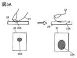
図5Aに、表示部20と、指22と、1回目の撮像画像26と、2回目の撮像画像27と、を模式的に示している。図5Aでは、指22が表示部20に触れており、時間経過に伴い接触領域22Aの面積が大きくなっている。1回目の撮像画像26と2回目の撮像画像27の接触領域22Aの面積の差が算出され、基準の接触面積の変化量より差が大きい場合、第1の処理が実行される。なお、撮像の頻度、及び、撮像の間隔は、それぞれ、適宜設定することができる。5A shows a schematic diagram of the
図5Bに、表示部20と、指22と、1回目の撮像画像28と、2回目の撮像画像29と、を模式的に示している。図5Bでは、指22が表示部20に触れており、時間経過に伴う接触領域22Aの面積の変化が、図5Aに比べて小さい。1回目の撮像画像28と2回目の撮像画像29の接触面積の差が算出され、基準の接触面積の変化量より差が小さい場合、第2の処理が実行される。Fig. 5B shows a schematic diagram of the
本実施の形態は、他の実施の形態と適宜組み合わせることができる。また、本明細書において、1つの実施の形態の中に、複数の構成例が示される場合は、構成例を適宜組み合わせることが可能である。This embodiment mode can be combined with other embodiment modes as appropriate. In addition, in the case where a plurality of configuration examples are shown in one embodiment mode in this specification, the configuration examples can be combined as appropriate.
(実施の形態2)
本実施の形態では、本発明の一態様の表示装置について図6~図15を用いて説明する。(Embodiment 2)
In this embodiment, a display device according to one embodiment of the present invention will be described with reference to FIGS.
本実施の形態の表示装置は、実施の形態1で説明したデバイスの表示部に好適に用いることができる。The display device of this embodiment mode can be suitably used for a display portion of the device described in Embodiment Mode 1.
本発明の一態様の表示装置の表示部は、発光素子(発光デバイスともいう)を用いて画像を表示する機能を有する。さらに、当該表示部は、撮像機能及びセンシング機能の一方または双方も有する。A display portion of a display device according to one embodiment of the present invention has a function of displaying an image using a light-emitting element (also referred to as a light-emitting device). Further, the display portion has one or both of an imaging function and a sensing function.
本発明の一態様の表示装置は、受光素子(受光デバイスともいう)と発光素子とを有する。または、本発明の一態様の表示装置は、受発光素子(受発光デバイスともいう)と発光素子とを有する。A display device according to one embodiment of the present invention includes a light-receiving element (also referred to as a light-receiving device) and a light-emitting element. Alternatively, a display device according to one embodiment of the present invention includes a light-receiving and light-emitting element (also referred to as a light-receiving and light-emitting device) and a light-emitting element.
まず、受光素子と発光素子とを有する表示装置について説明する。First, a display device having a light receiving element and a light emitting element will be described.
本発明の一態様の表示装置は、表示部に、受光素子と発光素子とを有する。本発明の一態様の表示装置は、表示部に、発光素子がマトリクス状に配置されており、当該表示部で画像を表示することができる。また、当該表示部には、受光素子がマトリクス状に配置されており、表示部は、撮像機能及びセンシング機能の一方または双方も有する。表示部は、イメージセンサやタッチセンサに用いることができる。つまり、表示部で光を検出することで、画像を撮像することや、対象物(指やペンなど)の近接もしくは接触を検出することができる。さらに、本発明の一態様の表示装置は、発光素子をセンサの光源として利用することができる。したがって、表示装置と別に受光部及び光源を設けなくてよく、電子機器の部品点数を削減することができる。A display device according to one embodiment of the present invention includes a light-receiving element and a light-emitting element in a display portion. In the display device according to one embodiment of the present invention, light-emitting elements are arranged in a matrix in the display portion, and an image can be displayed on the display portion. In addition, light-receiving elements are arranged in a matrix in the display portion, and the display portion has one or both of an imaging function and a sensing function. The display portion can be used as an image sensor or a touch sensor. That is, by detecting light in the display portion, an image can be captured or the proximity or contact of an object (such as a finger or a pen) can be detected. Furthermore, in the display device according to one embodiment of the present invention, the light-emitting element can be used as a light source for a sensor. Therefore, it is not necessary to provide a light-receiving portion and a light source separately from the display device, and the number of components of an electronic device can be reduced.
本発明の一態様の表示装置では、表示部が有する発光素子が発した光を対象物が反射(または散乱)した際、受光素子がその反射光(または散乱光)を検出できるため、暗い場所でも、撮像やタッチ操作の検出が可能である。In a display device of one embodiment of the present invention, when light emitted by a light-emitting element in a display portion is reflected (or scattered) by an object, a light-receiving element can detect the reflected light (or scattered light); therefore, imaging and touch operation detection are possible even in a dark place.
本発明の一態様の表示装置は、発光素子を用いて、画像を表示する機能を有する。つまり、発光素子は、表示素子(表示デバイスともいう)として機能する。A display device according to one embodiment of the present invention has a function of displaying an image using a light-emitting element, that is, the light-emitting element functions as a display element (also referred to as a display device).
発光素子としては、OLED(Organic Light Emitting Diode)やQLED(Quantum-dot Light Emitting Diode)などのEL素子(ELデバイスともいう)を用いることが好ましい。EL素子が有する発光物質としては、蛍光を発する物質(蛍光材料)、燐光を発する物質(燐光材料)、無機化合物(量子ドット材料など)、熱活性化遅延蛍光を示す物質(熱活性化遅延蛍光(Thermally Activated Delayed Fluorescence:TADF)材料)などが挙げられる。また、発光素子として、マイクロLED(Light Emitting Diode)などのLEDを用いることもできる。As the light-emitting element, it is preferable to use an EL element (also called an EL device) such as an OLED (organic light-emitting diode) or a QLED (quantum-dot light-emitting diode). Examples of light-emitting substances that the EL element has include a substance that emits fluorescence (fluorescent material), a substance that emits phosphorescence (phosphorescent material), an inorganic compound (such as a quantum dot material), and a substance that exhibits thermally activated delayed fluorescence (thermally activated delayed fluorescence (TADF) material). In addition, an LED such as a micro LED (light-emitting diode) can also be used as the light-emitting element.
本発明の一態様の表示装置は、受光素子を用いて、光を検出する機能を有する。A display device according to one embodiment of the present invention has a function of detecting light using a light-receiving element.
受光素子をイメージセンサに用いる場合、表示装置は、受光素子を用いて、画像を撮像することができる。例えば、本実施の形態の表示装置は、スキャナとして用いることができる。When the light receiving element is used as an image sensor, the display device can capture an image using the light receiving element. For example, the display device of the present embodiment can be used as a scanner.
例えば、イメージセンサを用いて、指紋、掌紋などの生体情報に係るデータを取得することができる。つまり、表示装置に、生体認証用センサを内蔵させることができる。表示装置が生体認証用センサを内蔵することで、表示装置とは別に生体認証用センサを設ける場合に比べて、電子機器の部品点数を少なくでき、電子機器の小型化及び軽量化が可能である。For example, an image sensor can be used to acquire data related to biometric information such as fingerprints and palm prints. In other words, a biometric authentication sensor can be built into the display device. By building a biometric authentication sensor into the display device, the number of components in the electronic device can be reduced, and the electronic device can be made smaller and lighter, compared to a case in which a biometric authentication sensor is provided separately from the display device.
また、受光素子をタッチセンサに用いる場合、表示装置は、受光素子を用いて、対象物の近接または接触を検出することができる。Furthermore, when the light receiving element is used as a touch sensor, the display device can detect the proximity or contact of an object by using the light receiving element.
受光素子としては、例えば、pn型またはpin型のフォトダイオードを用いることができる。受光素子は、受光素子に入射する光を検出し電荷を発生させる光電変換素子(光電変換デバイスともいう)として機能する。受光素子に入射する光量に基づき、受光素子から発生する電荷量が決まる。The light receiving element may be, for example, a pn-type or pin-type photodiode. The light receiving element functions as a photoelectric conversion element (also called a photoelectric conversion device) that detects light incident on the light receiving element and generates electric charge. The amount of electric charge generated by the light receiving element is determined based on the amount of light incident on the light receiving element.
特に、受光素子として、有機化合物を含む層を有する有機フォトダイオードを用いることが好ましい。有機フォトダイオードは、薄型化、軽量化、及び大面積化が容易であり、また、形状及びデザインの自由度が高いため、様々な表示装置に適用できる。In particular, it is preferable to use an organic photodiode having a layer containing an organic compound as the light receiving element. Organic photodiodes can be easily made thin, lightweight, and large in area, and have a high degree of freedom in shape and design, and therefore can be applied to various display devices.
本発明の一態様では、発光素子として有機EL素子(有機ELデバイスともいう)を用い、受光素子として有機フォトダイオードを用いる。有機EL素子及び有機フォトダイオードは、同一基板上に形成することができる。したがって、有機EL素子を用いた表示装置に有機フォトダイオードを内蔵することができる。In one embodiment of the present invention, an organic EL element (also referred to as an organic EL device) is used as a light-emitting element, and an organic photodiode is used as a light-receiving element. The organic EL element and the organic photodiode can be formed over the same substrate. Therefore, the organic photodiode can be built into a display device using the organic EL element.
有機EL素子及び有機フォトダイオードを構成する全ての層を作り分けようとすると、成膜工程が非常に多くなる。有機フォトダイオードは、有機EL素子と共通の構成にできる層が多いため、共通の構成にできる層は一括で成膜することで、成膜工程の増加を抑制することができる。If all layers constituting an organic EL element and an organic photodiode are to be fabricated separately, the number of film formation steps will be extremely large. Since many layers of an organic photodiode can be made common to an organic EL element and an organic EL element, the layers that can be made common can be formed in a single process, thereby suppressing the increase in film formation steps.
例えば、一対の電極のうち一方(共通電極)を、受光素子及び発光素子で共通の層とすることができる。また、例えば、正孔注入層、正孔輸送層、電子輸送層、及び電子注入層の少なくとも1つを、受光素子及び発光素子で共通の層とすることが好ましい。また、例えば、受光素子が活性層を有し、発光素子が発光層を有する以外は、受光素子と発光素子とで同一の構成にすることもできる。つまり、発光素子の発光層を、活性層に置き換えるのみで、受光素子を作製することもできる。このように、受光素子及び発光素子が共通の層を有することで、成膜回数及びマスクの数を減らすことができ、表示装置の作製工程及び作製コストを削減することができる。また、表示装置の既存の製造装置及び製造方法を用いて、受光素子を有する表示装置を作製することができる。For example, one of the pair of electrodes (common electrode) can be a layer common to the light receiving element and the light emitting element. In addition, for example, at least one of the hole injection layer, the hole transport layer, the electron transport layer, and the electron injection layer is preferably a layer common to the light receiving element and the light emitting element. In addition, for example, the light receiving element and the light emitting element can be configured to be the same except that the light receiving element has an active layer and the light emitting element has a light emitting layer. In other words, the light receiving element can be manufactured by simply replacing the light emitting layer of the light emitting element with the active layer. In this way, by having the light receiving element and the light emitting element have a common layer, the number of film formations and the number of masks can be reduced, and the manufacturing process and manufacturing cost of the display device can be reduced. In addition, a display device having a light receiving element can be manufactured using an existing manufacturing device and manufacturing method for a display device.
なお、受光素子と発光素子が共通で有する層は、発光素子における機能と受光素子における機能とが異なる場合がある。本明細書中では、発光素子における機能に基づいて構成要素を呼称する。例えば、正孔注入層は、発光素子において正孔注入層として機能し、受光素子において正孔輸送層として機能する。同様に、電子注入層は、発光素子において電子注入層として機能し、受光素子において電子輸送層として機能する。また、受光素子と発光素子が共通で有する層は、発光素子における機能と受光素子における機能とが同一である場合もある。正孔輸送層は、発光素子及び受光素子のいずれにおいても、正孔輸送層として機能し、電子輸送層は、発光素子及び受光素子のいずれにおいても、電子輸送層として機能する。In addition, the layer shared by the light receiving element and the light emitting element may have different functions in the light emitting element and the light receiving element. In this specification, the components are named based on their functions in the light emitting element. For example, the hole injection layer functions as a hole injection layer in the light emitting element and functions as a hole transport layer in the light receiving element. Similarly, the electron injection layer functions as an electron injection layer in the light emitting element and functions as an electron transport layer in the light receiving element. In addition, the layer shared by the light receiving element and the light emitting element may have the same functions in the light emitting element and the light receiving element. The hole transport layer functions as a hole transport layer in both the light emitting element and the light receiving element, and the electron transport layer functions as an electron transport layer in both the light emitting element and the light receiving element.
次に、受発光素子と発光素子とを有する表示装置について説明する。Next, a display device having light emitting and receiving elements and a light emitting element will be described.
本発明の一態様の表示装置において、いずれかの色を呈する副画素は、発光素子の代わりとして、受発光素子を有し、その他の色を呈する副画素は、発光素子を有する。受発光素子は、光を発する機能(発光機能)と、受光する機能(受光機能)と、の双方を有する。例えば、画素が、赤色の副画素、緑色の副画素、青色の副画素の3つの副画素を有する場合、少なくとも1つの副画素が受発光素子を有し、他の副画素は発光素子を有する構成とする。したがって、本発明の一態様の表示装置の表示部は、受発光素子と発光素子との双方を用いて画像を表示する機能を有する。In a display device according to one embodiment of the present invention, a subpixel that exhibits one of the colors has a light-receiving and light-emitting element instead of a light-emitting element, and a subpixel that exhibits the other color has a light-emitting element. The light-receiving and light-emitting element has both a function of emitting light (light-emitting function) and a function of receiving light (light-receiving function). For example, when a pixel has three subpixels, a red subpixel, a green subpixel, and a blue subpixel, at least one subpixel has a light-receiving and light-emitting element, and the other subpixels have light-emitting elements. Thus, a display portion of the display device according to one embodiment of the present invention has a function of displaying an image using both the light-receiving and light-emitting elements and the light-emitting elements.
受発光素子が、発光素子と受光素子とを兼ねることで、画素に含まれる副画素の数を増やさずに、画素に受光機能を付与することができる。これにより、画素の開口率(各副画素の開口率)、及び、表示装置の精細度を維持したまま、表示装置の表示部に、撮像機能及びセンシング機能の一方または双方を付加することができる。したがって、本発明の一態様の表示装置は、発光素子を有する副画素とは別に、受光素子を有する副画素を設ける場合に比べ、画素の開口率を高くでき、また、高精細化が容易である。Since the light receiving/emitting element serves as both a light emitting element and a light receiving element, a light receiving function can be imparted to the pixel without increasing the number of subpixels included in the pixel. As a result, one or both of an imaging function and a sensing function can be added to the display portion of the display device while maintaining the aperture ratio of the pixel (aperture ratio of each subpixel) and the resolution of the display device. Therefore, the display device of one embodiment of the present invention can have a higher aperture ratio of the pixel and can easily achieve high resolution, compared to the case where a subpixel having a light receiving element is provided in addition to a subpixel having a light emitting element.
本発明の一態様の表示装置は、表示部に、受発光素子と発光素子がマトリクス状に配置されており、当該表示部で画像を表示することができる。また、表示部は、イメージセンサやタッチセンサに用いることができる。本発明の一態様の表示装置は、発光素子をセンサの光源として利用することができる。したがって、表示装置と別に受光部及び光源を設けなくてよく、電子機器の部品点数を削減することができる。In a display device according to one embodiment of the present invention, a light-receiving and light-emitting element are arranged in a matrix in a display portion, and an image can be displayed on the display portion. The display portion can be used as an image sensor or a touch sensor. In the display device according to one embodiment of the present invention, the light-emitting element can be used as a light source of a sensor. Therefore, it is not necessary to provide a light-receiving portion and a light source separately from the display device, and the number of components of an electronic device can be reduced.
本発明の一態様の表示装置では、表示部が有する発光素子が発した光を対象物が反射(または散乱)した際、受発光素子がその反射光(または散乱光)を検出できるため、暗い場所でも、撮像やタッチ操作の検出が可能である。In a display device of one embodiment of the present invention, when light emitted by a light-emitting element in a display portion is reflected (or scattered) by an object, the light-receiving and light-emitting element can detect the reflected light (or scattered light); therefore, imaging and touch operation can be detected even in a dark place.
受発光素子は、有機EL素子と有機フォトダイオードを組み合わせて作製することができる。例えば、有機EL素子の積層構造に、有機フォトダイオードの活性層を追加することで、受発光素子を作製することができる。さらに、有機EL素子と有機フォトダイオードを組み合わせて作製する受発光素子は、有機EL素子と共通の構成にできる層を一括で成膜することで、成膜工程の増加を抑制することができる。The light-receiving and light-emitting element can be fabricated by combining an organic EL element and an organic photodiode. For example, the light-receiving and light-emitting element can be fabricated by adding an active layer of an organic photodiode to a laminated structure of an organic EL element. Furthermore, the light-receiving and light-emitting element fabricated by combining an organic EL element and an organic photodiode can suppress an increase in the number of film-forming steps by forming layers that can be configured in common with the organic EL element in a single step.
例えば、一対の電極のうち一方(共通電極)を、受発光素子及び発光素子で共通の層とすることができる。また、例えば、正孔注入層、正孔輸送層、電子輸送層、及び電子注入層の少なくとも1つを、受発光素子及び発光素子で共通の層とすることが好ましい。また、例えば、受光素子の活性層の有無以外は、受発光素子と発光素子とで同一の構成にすることもできる。つまり、発光素子に、受光素子の活性層を加えるのみで、受発光素子を作製することもできる。このように、受発光素子及び発光素子が共通の層を有することで、成膜回数及びマスクの数を減らすことができ、表示装置の作製工程及び作製コストを削減することができる。また、表示装置の既存の製造装置及び製造方法を用いて、受発光素子を有する表示装置を作製することができる。For example, one of the pair of electrodes (common electrode) can be a layer common to the light-receiving and light-emitting elements and the light-emitting elements. In addition, it is preferable that at least one of the hole injection layer, the hole transport layer, the electron transport layer, and the electron injection layer is a layer common to the light-receiving and light-emitting elements and the light-emitting elements. In addition, for example, the light-receiving and light-emitting elements and the light-emitting elements can be configured to be the same except for the presence or absence of the active layer of the light-receiving element. In other words, the light-receiving and light-emitting elements can be manufactured by simply adding the active layer of the light-receiving element to the light-emitting element. In this way, by having the light-receiving and light-emitting elements and the light-emitting elements having a common layer, the number of film formations and the number of masks can be reduced, and the manufacturing process and manufacturing cost of the display device can be reduced. In addition, a display device having a light-receiving and light-emitting element can be manufactured using an existing manufacturing device and manufacturing method for a display device.
なお、受発光素子が有する層は、受発光素子が、受光素子として機能する場合と、発光素子として機能する場合と、で、機能が異なることがある。本明細書中では、受発光素子が発光素子として機能する場合における機能に基づいて構成要素を呼称する。例えば、正孔注入層は、受発光素子が発光素子として機能する際には、正孔注入層として機能し、受発光素子が受光素子として機能する際には、正孔輸送層として機能する。同様に、電子注入層は、受発光素子が発光素子として機能する際には、電子注入層として機能し、受発光素子が受光素子として機能する際には、電子輸送層として機能する。また、受発光素子が有する層は、受発光素子が、受光素子として機能する場合と、発光素子として機能する場合と、で、機能が同一であることもある。正孔輸送層は、発光素子及び受光素子のいずれとして機能する場合においても、正孔輸送層として機能し、電子輸送層は、発光素子及び受光素子のいずれとして機能する場合においても、電子輸送層として機能する。The layers of the light-receiving/light-emitting element may have different functions when the light-receiving/light-emitting element functions as a light-receiving element and when it functions as a light-emitting element. In this specification, the components are named based on the functions when the light-receiving/light-emitting element functions as a light-emitting element. For example, the hole injection layer functions as a hole injection layer when the light-receiving/light-emitting element functions as a light-emitting element, and functions as a hole transport layer when the light-receiving/light-emitting element functions as a light-receiving element. Similarly, the electron injection layer functions as an electron injection layer when the light-receiving/light-emitting element functions as a light-emitting element, and functions as an electron transport layer when the light-receiving/light-emitting element functions as a light-receiving element. In addition, the layers of the light-receiving/light-emitting element may have the same functions when the light-receiving/light-emitting element functions as a light-receiving element and when it functions as a light-emitting element. The hole transport layer functions as a hole transport layer when the light-receiving/light-emitting element functions as a light-emitting element and a light-receiving element, and the electron transport layer functions as an electron transport layer when the light-receiving/light-emitting element functions as a light-emitting element and a light-receiving element.
本実施の形態の表示装置は、発光素子及び受発光素子を用いて、画像を表示する機能を有する。つまり、発光素子及び受発光素子は、表示素子として機能する。The display device of this embodiment has a function of displaying an image using a light-emitting element and a light-receiving and light-emitting element, that is, the light-emitting element and the light-receiving and light-emitting element function as display elements.
本実施の形態の表示装置は、受発光素子を用いて、光を検出する機能を有する。受発光素子は、受発光素子自身が発する光よりも短波長の光を検出することができる。The display device of this embodiment has a function of detecting light by using a light receiving and emitting element, which can detect light having a shorter wavelength than light emitted by the light receiving and emitting element itself.
受発光素子をイメージセンサに用いる場合、本実施の形態の表示装置は、受発光素子を用いて、画像を撮像することができる。例えば、本実施の形態の表示装置は、スキャナとして用いることができる。When the light emitting/receiving element is used in an image sensor, the display device of this embodiment can capture an image using the light emitting/receiving element. For example, the display device of this embodiment can be used as a scanner.
また、受発光素子をタッチセンサに用いる場合、本実施の形態の表示装置は、受発光素子を用いて、対象物の近接または接触を検出することができる。When the light emitting/receiving element is used as a touch sensor, the display device of this embodiment can detect the proximity or contact of an object by using the light emitting/receiving element.
受発光素子は、受発光素子に入射する光を検出し電荷を発生させる光電変換素子として機能する。受発光素子に入射する光量に基づき、受発光素子から発生する電荷量が決まる。The light emitting/receiving element functions as a photoelectric conversion element that detects light incident on the light emitting/receiving element and generates electric charge. The amount of electric charge generated by the light emitting/receiving element is determined based on the amount of light incident on the light emitting/receiving element.
受発光素子は、上記発光素子の構成に、受光素子の活性層を追加することで作製することができる。The light receiving/emitting element can be fabricated by adding an active layer of a light receiving element to the above-mentioned light emitting element.
受発光素子には、例えば、pn型またはpin型のフォトダイオード構造を適用することができる。The light emitting/receiving element may have, for example, a pn-type or pin-type photodiode structure.
特に、受発光素子には、有機化合物を含む層を有する有機フォトダイオードの活性層を用いることが好ましい。有機フォトダイオードは、薄型化、軽量化、及び大面積化が容易であり、また、形状及びデザインの自由度が高いため、様々な表示装置に適用できる。In particular, it is preferable to use an active layer of an organic photodiode having a layer containing an organic compound for the light-receiving and light-emitting element. Organic photodiodes can be easily made thin, lightweight, and large in area, and have a high degree of freedom in shape and design, making them applicable to a variety of display devices.
以下では、本発明の一態様の表示装置について、図面を用いてより具体的に説明する。The display device of one embodiment of the present invention will be described more specifically below with reference to the drawings.
[表示装置]
図6A~図6D及び図6Fに、本発明の一態様の表示装置の断面図を示す。[Display Device]
6A to 6D and 6F each show a cross-sectional view of a display device according to one embodiment of the present invention.
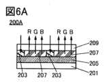
図6Aに示す表示装置200Aは、基板201と基板209との間に、受光素子を有する層203、機能層205、及び、発光素子を有する層207を有する。A
表示装置200Aは、発光素子を有する層207から、赤色(R)、緑色(G)、及び青色(B)の光が射出される構成である。The
受光素子を有する層203に含まれる受光素子は、表示装置200Aの外部から入射した光を検出することができる。The light receiving elements included in the
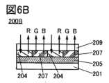
図6Bに示す表示装置200Bは、基板201と基板209との間に、受発光素子を有する層204、機能層205、及び、発光素子を有する層207を有する。A
表示装置200Bは、発光素子を有する層207から、緑色(G)の光及び青色(B)の光が射出され、受発光素子を有する層204から赤色(R)の光が射出される構成である。なお、本発明の一態様の表示装置において、受発光素子を有する層204が発する光の色は、赤色に限定されない。また、発光素子を有する層207が発する光の色も、緑色と青色の組み合わせに限定されない。The
受発光素子を有する層204に含まれる受発光素子は、表示装置200Bの外部から入射した光を検出することができる。当該受発光素子は、例えば、緑色(G)の光及び青色(B)の光のうち一方または双方を検出することができる。The light emitting/receiving elements included in the
機能層205は、受光素子または受発光素子を駆動する回路、及び、発光素子を駆動する回路を有する。機能層205には、スイッチ、トランジスタ、容量、抵抗、配線、端子などを設けることができる。なお、発光素子及び受光素子をパッシブマトリクス方式で駆動させる場合には、スイッチやトランジスタを設けない構成としてもよい。The
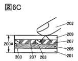
本発明の一態様の表示装置は、表示装置に接触している指などの対象物を検出する機能(タッチパネルとしての機能)を有していてもよい。例えば、図6Cに示すように、発光素子を有する層207において発光素子が発した光を、表示装置200Aに接触した指202が反射することで、受光素子を有する層203における受光素子がその反射光を検出する。これにより、表示装置200Aに指202が接触したことを検出することができる。また、表示装置200Bでは、発光素子を有する層207において発光素子が発した光を、表示装置200Bに接触した指が反射することで、受発光素子を有する層204における受発光素子がその反射光を検出することができる。なお、以下では、発光素子の発光が対象物により反射される場合を例に挙げて説明するが、光は対象物により散乱される場合もある。The display device according to one embodiment of the present invention may have a function of detecting an object such as a finger in contact with the display device (a function as a touch panel). For example, as shown in FIG. 6C , light emitted by a light-emitting element in the
本発明の一態様の表示装置は、図6Dに示すように、表示装置に近接している(接触していない)対象物を検出または撮像する機能を有していてもよい。The display device of one embodiment of the present invention may have a function of detecting or capturing an image of an object that is close to (not in contact with) the display device, as shown in FIG. 6D.
本発明の一態様の表示装置は、指202の指紋を検出する機能を有していてもよい。図6Eに、本発明の一態様の表示装置で撮像した画像のイメージ図を示す。図6Eには、撮像範囲263内に、指202の輪郭を破線で、接触部261の輪郭を一点鎖線で示している。接触部261内において、受光素子(または受発光素子)に入射する光量の違いによって、コントラストの高い指紋262の画像を撮像することができる。The display device of one embodiment of the present invention may have a function of detecting a fingerprint of a
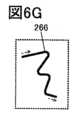
本発明の一態様の表示装置は、ペンタブレットとしても機能させることができる。図6Fには、スタイラス208の先端を基板209に接触させた状態で、破線矢印の方向に滑らせている様子を示している。The display device of one embodiment of the present invention can also function as a pen tablet. Fig. 6F shows a state in which the tip of a
図6Fに示すように、スタイラス208の先端と、基板209の接触面で散乱される散乱光が、当該接触面と重なる部分に位置する受光素子(または受発光素子)に入射することで、スタイラス208の先端の位置を高精度に検出することができる。As shown in Figure 6F, the scattered light scattered between the tip of the
図6Gに、本発明の一態様の表示装置で検出したスタイラス208の軌跡266の例を示している。本発明の一態様の表示装置は、高い位置精度でスタイラス208等の被検出体の位置検出が可能であるため、描画アプリケーション等において、高精細な描画を行うことも可能である。また、静電容量式のタッチセンサや、電磁誘導型のタッチペン等を用いた場合とは異なり、絶縁性の高い被検出体であっても位置検出が可能であるため、スタイラス208の先端部の材料は問われず、様々な筆記用具(例えば筆、ガラスペン、羽ペンなど)を用いることもできる。6G shows an example of a
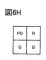
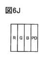
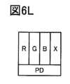
[画素]
本発明の一態様の表示装置は、マトリクス状に配置された複数の画素を有する。1つの画素は、複数の副画素を有する。1つの副画素は、1つの発光素子、1つの受発光素子、または1つの受光素子を有する。[Pixels]
A display device according to one embodiment of the present invention includes a plurality of pixels arranged in a matrix, and each pixel includes a plurality of sub-pixels, each of which includes one light-emitting element, one light-receiving light-emitting element, or one light-receiving element.
複数の画素は、それぞれ、発光素子を有する副画素、受光素子を有する副画素、及び、受発光素子を有する副画素のうち1つまたは複数を有する。Each of the pixels has one or more of a sub-pixel having a light-emitting element, a sub-pixel having a light-receiving element, and a sub-pixel having a light-receiving or light-emitting element.
例えば、画素は、発光素子を有する副画素を複数(例えば、3つまたは4つ)有し、受光素子を有する副画素を1つ有する。For example, a pixel has multiple (eg, three or four) sub-pixels that have a light-emitting element, and one sub-pixel that has a light-receiving element.
なお、受光素子は、全ての画素に設けられていてもよく、一部の画素に設けられていてもよい。また、1つの画素が複数の受光素子を有していてもよい。また、1つの受光素子が複数の画素にわたって設けられていてもよい。受光素子の精細度と発光素子の精細度は互いに異なっていてもよい。The light receiving element may be provided in all pixels or in some pixels. Also, one pixel may have multiple light receiving elements. Also, one light receiving element may be provided across multiple pixels. The resolution of the light receiving element and the resolution of the light emitting element may be different from each other.
画素が発光素子を有する副画素を3つ有する場合、当該3つの副画素としては、R、G、Bの3色の副画素、黄色(Y)、シアン(C)、及びマゼンタ(M)の3色の副画素などが挙げられる。画素が発光素子を有する副画素を4つ有する場合、当該4つの副画素としては、R、G、B、白色(W)の4色の副画素、R、G、B、Yの4色の副画素などが挙げられる。When a pixel has three subpixels each having a light-emitting element, the three subpixels may include subpixels of three colors of R, G, and B, or subpixels of three colors of yellow (Y), cyan (C), and magenta (M), etc. When a pixel has four subpixels each having a light-emitting element, the four subpixels may include subpixels of four colors of R, G, B, and white (W), or subpixels of four colors of R, G, B, and Y, etc.
図6H、図6J、図6K、図6Lに、発光素子を有する副画素を複数有し、受光素子を有する副画素を1つ有する画素の一例を示す。なお、本実施の形態で示す副画素の配列は図示した順序に限定されない。例えば、副画素(B)と副画素(G)の位置を逆にしても構わない。6H, 6J, 6K, and 6L show an example of a pixel having a plurality of subpixels each having a light-emitting element and one subpixel each having a light-receiving element. Note that the arrangement of the subpixels shown in this embodiment is not limited to the order shown in the drawings. For example, the positions of the subpixels (B) and (G) may be reversed.
図6H、図6J、図6Kに示す画素は、いずれも、受光機能を有する副画素(PD)、赤色の光を呈する副画素(R)、緑色の光を呈する副画素(G)、及び、青色の光を呈する副画素(B)を有する。Each of the pixels shown in Figures 6H, 6J, and 6K has a sub-pixel (PD) having a light receiving function, a sub-pixel (R) that emits red light, a sub-pixel (G) that emits green light, and a sub-pixel (B) that emits blue light.
図6Hに示す画素には、マトリクス配列が適用されており、図6Jに示す画素には、ストライプ配列が適用されている。また、図6Kは、横1列に、赤色の光を呈する副画素(R)、緑色の光を呈する副画素(G)、及び、青色の光を呈する副画素(B)が配置され、その下に受光機能を有する副画素(PD)が配置されている例である。つまり、図6Kにおいて、副画素(R)、副画素(G)、及び副画素(B)は互いに同じ行に配置され、副画素(PD)とは異なる行に配置される。A matrix arrangement is applied to the pixel shown in Fig. 6H, and a stripe arrangement is applied to the pixel shown in Fig. 6J. Fig. 6K shows an example in which a sub-pixel (R) that emits red light, a sub-pixel (G) that emits green light, and a sub-pixel (B) that emits blue light are arranged in one horizontal row, and a sub-pixel (PD) having a light receiving function is arranged below them. In other words, in Fig. 6K, the sub-pixels (R), (G), and (B) are arranged in the same row, and are arranged in a different row from the sub-pixel (PD).
図6Lに示す画素は、図6Kに示す画素の構成に加えて、R、G、B以外の光を呈する副画素(X)を有する。R、G、B以外の光としては、白色(W)、黄色(Y)、シアン(C)、マゼンタ(M)、赤外光(IR)等の光が挙げられる。副画素(X)が赤外光を呈する場合、受光機能を有する副画素(PD)は、赤外光を検出する機能を有することが好ましい。受光機能を有する副画素(PD)は、可視光及び赤外光の双方を検出する機能を有していてもよい。センサの用途に応じて、受光素子が検出する光の波長を決定することができる。The pixel shown in FIG. 6L has a sub-pixel (X) that exhibits light other than R, G, and B in addition to the configuration of the pixel shown in FIG. 6K. Examples of light other than R, G, and B include white (W), yellow (Y), cyan (C), magenta (M), and infrared light (IR). When the sub-pixel (X) exhibits infrared light, the sub-pixel (PD) having a light receiving function preferably has a function of detecting infrared light. The sub-pixel (PD) having a light receiving function may have a function of detecting both visible light and infrared light. The wavelength of light detected by the light receiving element can be determined according to the application of the sensor.
または、例えば、画素は、発光素子を有する副画素を複数有し、受発光素子を有する副画素を1つ有する。Alternatively, for example, a pixel has a plurality of sub-pixels each having a light-emitting element, and has one sub-pixel each having a light-receiving or light-emitting element.
受発光素子を有する表示装置は、画素に受光機能を組み込むために画素配列を変更する必要がないため、開口率及び精細度を低減させずに、表示部に撮像機能及びセンシング機能の一方または双方を付加することができる。A display device having light receiving and emitting elements does not require changing the pixel arrangement to incorporate a light receiving function into the pixel, and therefore can add an imaging function and/or a sensing function to the display section without reducing the aperture ratio and resolution.
なお、受発光素子は、全ての画素に設けられていてもよく、一部の画素に設けられていてもよい。また、1つの画素が複数の受発光素子を有していてもよい。Note that the light emitting/receiving elements may be provided in all or some of the pixels, and one pixel may have a plurality of light emitting/receiving elements.
図7A~図7Dに、発光素子を有する副画素を複数有し、受発光素子を有する副画素を1つ有する画素の一例を示す。7A to 7D show an example of a pixel having a plurality of sub-pixels each having a light-emitting element, and one sub-pixel each having a light-receiving or light-emitting element.
図7Aに示す画素は、ストライプ配列が適用され、赤色の光を呈し、かつ、受光機能を有する副画素(R・PD)、緑色の光を呈する副画素(G)、及び、青色の光を呈する副画素(B)を有する。画素が、R、G、Bの3つの副画素からなる表示装置において、Rの副画素に用いる発光素子を、受発光素子に置き換えることで、画素に受光機能を有する表示装置を作製することができる。7A is a display device in which a pixel has a light receiving function, and includes a subpixel (R PD) that emits red light, a subpixel (G) that emits green light, and a subpixel (B) that emits blue light. In a display device in which a pixel is composed of three subpixels, R, G, and B, a light emitting element used in the R subpixel can be replaced with a light receiving/emitting element, thereby making it possible to manufacture a display device in which the pixel has a light receiving function.
図7Bに示す画素は、赤色の光を呈し、かつ、受光機能を有する副画素(R・PD)、緑色の光を呈する副画素(G)、及び、青色の光を呈する副画素(B)を有する。副画素(R・PD)は、副画素(G)と副画素(B)とは異なる列に配置される。副画素(G)と副画素(B)とは、同じ列に交互に配置され、一方が奇数行に設けられ、他方が偶数行に設けられる。なお、他の色の副画素と異なる列に配置される副画素は、赤色(R)に限られず、緑色(G)または青色(B)であってもよい。The pixel shown in Fig. 7B has a subpixel (R-PD) that emits red light and has a light receiving function, a subpixel (G) that emits green light, and a subpixel (B) that emits blue light. The subpixel (R-PD) is arranged in a column different from the subpixels (G) and (B). The subpixels (G) and (B) are arranged alternately in the same column, with one being arranged in an odd-numbered row and the other being arranged in an even-numbered row. Note that the subpixels arranged in a column different from the subpixels of the other colors are not limited to red (R) and may be green (G) or blue (B).
図7Cに示す画素は、マトリクス配列が適用され、赤色の光を呈し、かつ、受光機能を有する副画素(R・PD)、緑色の光を呈する副画素(G)、青色の光を呈する副画素(B)、及び、R、G、B以外の光を呈する副画素(X)を有する。画素が、R、G、B、Xの4つの副画素からなる表示装置においても、Rの副画素に用いる発光素子を、受発光素子に置き換えることで、画素に受光機能を有する表示装置を作製することができる。7C is arranged in a matrix and has a subpixel (R PD) that emits red light and has a light receiving function, a subpixel (G) that emits green light, a subpixel (B) that emits blue light, and a subpixel (X) that emits light other than R, G, and B. Even in a display device in which a pixel is composed of four subpixels, R, G, B, and X, a display device in which the pixel has a light receiving function can be manufactured by replacing the light emitting element used in the R subpixel with a light receiving/emitting element.
図7Dには、2つの画素を示しており、点線で囲まれた3つの副画素により1つの画素が構成されている。図7Dに示す画素は、赤色の光を呈し、かつ、受光機能を有する副画素(R・PD)、緑色の光を呈する副画素(G)、及び、青色の光を呈する副画素(B)を有する。図7Dに示す左の画素では、副画素(R・PD)と同じ行に副画素(G)が配置され、副画素(R・PD)と同じ列に副画素(B)が配置されている。図7Dに示す右の画素では、副画素(R・PD)と同じ行に副画素(G)が配置され、副画素(G)と同じ列に副画素(B)が配置されている。図7Dに示す画素レイアウトでは、奇数行と偶数行のいずれにおいても、副画素(R・PD)、副画素(G)、及び副画素(B)が繰り返し配置されており、かつ、各列において、奇数行と偶数行では互いに異なる色の副画素が配置される。FIG. 7D shows two pixels, each of which is composed of three subpixels surrounded by dotted lines. The pixel shown in FIG. 7D has a subpixel (R·PD) that emits red light and has a light receiving function, a subpixel (G) that emits green light, and a subpixel (B) that emits blue light. In the left pixel shown in FIG. 7D, the subpixel (G) is arranged in the same row as the subpixel (R·PD), and the subpixel (B) is arranged in the same column as the subpixel (R·PD). In the right pixel shown in FIG. 7D, the subpixel (G) is arranged in the same row as the subpixel (R·PD), and the subpixel (B) is arranged in the same column as the subpixel (G). In the pixel layout shown in FIG. 7D, the subpixels (R·PD), (G), and (B) are repeatedly arranged in both odd and even rows, and in each column, subpixels of different colors are arranged in the odd and even rows.
図7Eには、ペンタイル配列が適用された4つの画素を示しており、隣接する2つの画素は組み合わせの異なる2色の光を呈する副画素を有する。なお、図7Eに示す副画素の形状は、当該副画素が有する発光素子または受発光素子の上面形状を示している。図7Fは、図7Eに示す画素配列の変形例である。Fig. 7E shows four pixels to which a Pentile arrangement is applied, and two adjacent pixels have sub-pixels that emit light of two different colors. Note that the shape of the sub-pixels shown in Fig. 7E shows the top shape of the light-emitting element or light-receiving element of the sub-pixel. Fig. 7F shows a modified example of the pixel arrangement shown in Fig. 7E.
図7Eに示す左上の画素と右下の画素は、赤色の光を呈し、かつ、受光機能を有する副画素(R・PD)、及び、緑色の光を呈する副画素(G)を有する。図7Eに示す左下の画素と右上の画素は、緑色の光を呈する副画素(G)、及び、青色の光を呈する副画素(B)を有する。The upper left pixel and the lower right pixel shown in Fig. 7E have a sub-pixel (R·PD) that emits red light and has a light receiving function, and a sub-pixel (G) that emits green light. The lower left pixel and the upper right pixel shown in Fig. 7E have a sub-pixel (G) that emits green light, and a sub-pixel (B) that emits blue light.
図7Fに示す左上の画素と右下の画素は、赤色の光を呈し、かつ、受光機能を有する副画素(R・PD)、及び、緑色の光を呈する副画素(G)を有する。図7Fに示す左下の画素と右上の画素は、赤色の光を呈し、かつ、受光機能を有する副画素(R・PD)、及び、青色の光を呈する副画素(B)を有する。The upper left pixel and the lower right pixel shown in Fig. 7F have a sub-pixel (R PD) that emits red light and has a light receiving function, and a sub-pixel (G) that emits green light. The lower left pixel and the upper right pixel shown in Fig. 7F have a sub-pixel (R PD) that emits red light and has a light receiving function, and a sub-pixel (B) that emits blue light.
図7Eでは、各画素に緑色の光を呈する副画素(G)が設けられている。一方、図7Fでは、各画素に赤色の光を呈し、かつ、受光機能を有する副画素(R・PD)が設けられている。各画素に受光機能を有する副画素が設けられているため、図7Fに示す構成では、図7Eに示す構成に比べて、高い精細度で撮像を行うことができる。これにより、例えば、生体認証の精度を高めることができる。In Fig. 7E, each pixel is provided with a sub-pixel (G) that emits green light. On the other hand, in Fig. 7F, each pixel is provided with a sub-pixel (R-PD) that emits red light and has a light receiving function. Since each pixel is provided with a sub-pixel that has a light receiving function, the configuration shown in Fig. 7F can capture images with higher resolution than the configuration shown in Fig. 7E. This can improve the accuracy of biometric authentication, for example.
また、発光素子及び受発光素子の上面形状は特に限定されず、円、楕円、多角形、角の丸い多角形等とすることができる。副画素(G)が有する発光素子の上面形状について、図7Eでは円形である例を示し、図7Fでは正方形である例を示している。各色の発光素子及び受発光素子の上面形状は、互いに異なっていてもよく、一部または全ての色で同じであってもよい。The top surface shapes of the light-emitting element and the light-receiving/light-emitting element are not particularly limited, and may be a circle, an ellipse, a polygon, a polygon with rounded corners, etc. With respect to the top surface shape of the light-emitting element of the subpixel (G), Fig. 7E shows an example in which it is a circle, and Fig. 7F shows an example in which it is a square. The top surface shapes of the light-emitting element and the light-receiving/light-emitting element of each color may be different from each other, or may be the same for some or all of the colors.
また、各色の副画素の開口率は、互いに異なっていてもよく、一部または全ての色で同じであってもよい。例えば、各画素に設けられる副画素(図7Eでは副画素(G)、図7Fでは副画素(R・PD))の開口率を、他の色の副画素の開口率に比べて小さくしてもよい。The aperture ratios of the sub-pixels of each color may be different from each other, or may be the same for some or all of the colors. For example, the aperture ratio of the sub-pixels (G in FIG. 7E and R/PD in FIG. 7F) provided in each pixel may be smaller than the aperture ratios of the sub-pixels of the other colors.
図7Gは、図7Fに示す画素配列の変形例である。具体的には、図7Gの構成は、図7Fの構成を45°回転させることで得られる。図7Fでは、2つの副画素により1つの画素が構成されることとして説明したが、図7Gに示すように、4つの副画素により1つの画素が構成されていると捉えることもできる。Fig. 7G is a modified example of the pixel array shown in Fig. 7F. Specifically, the configuration of Fig. 7G is obtained by rotating the configuration of Fig. 7F by 45°. Although Fig. 7F has been described as one pixel being composed of two sub-pixels, it can also be considered as one pixel being composed of four sub-pixels as shown in Fig. 7G.
図7Gでは、点線で囲まれた4つの副画素により1つの画素が構成されることとして説明を行う。1つの画素は、2つの副画素(R・PD)と、1つの副画素(G)と、1つの副画素(B)と、を有する。このように、1つの画素が、受光機能を有する副画素を複数有することで、高い精細度で撮像を行うことができる。したがって、生体認証の精度を高めることができる。例えば、撮像の精細度を、表示の精細度のルート2倍とすることができる。In FIG. 7G, a description will be given assuming that one pixel is composed of four sub-pixels surrounded by dotted lines. One pixel has two sub-pixels (R and PD), one sub-pixel (G), and one sub-pixel (B). In this way, one pixel has a plurality of sub-pixels having a light receiving function, so that imaging can be performed with high resolution. Therefore, the accuracy of biometric authentication can be improved. For example, the resolution of imaging can be set to the root of twice the resolution of display.
図7Fまたは図7Gに示す構成が適用された表示装置は、p個(pは2以上の整数)の第1の発光素子と、q個(qは2以上の整数)の第2の発光素子と、r個(rはpより大きく、qより大きい整数)の受発光素子と、を有する。pとrはr=2pを満たす。また、p、q、rはr=p+qを満たす。第1の発光素子と第2の発光素子のうち一方が緑色の光を発し、他方が青色の光を発する。受発光素子は、赤色の光を発し、かつ、受光機能を有する。A display device to which the configuration shown in Figure 7F or 7G is applied has p (p is an integer of 2 or more) first light-emitting elements, q (q is an integer of 2 or more) second light-emitting elements, and r (r is an integer greater than p and greater than q) light-receiving and light-emitting elements. p and r satisfy r = 2p. Furthermore, p, q, and r satisfy r = p + q. One of the first light-emitting elements and the second light-emitting elements emits green light, and the other emits blue light. The light-receiving and light-emitting elements emit red light and have a light-receiving function.
例えば、受発光素子を用いて、タッチ操作の検出を行う場合、光源からの発光がユーザーに視認されにくいことが好ましい。青色の光は、緑色の光よりも視認性が低いため、青色の光を発する発光素子を光源とすることが好ましい。したがって、受発光素子は、青色の光を受光する機能を有することが好ましい。For example, when detecting a touch operation using a light receiving/emitting element, it is preferable that the light emitted from the light source is difficult for the user to see. Since blue light is less visible than green light, it is preferable to use a light emitting element that emits blue light as the light source. Therefore, it is preferable that the light receiving/emitting element has a function of receiving blue light.
以上のように、本実施の形態の表示装置には、様々な配列の画素を適用することができる。As described above, pixels having various arrays can be applied to the display device of this embodiment mode.
[デバイス構造]
次に、本発明の一態様の表示装置に用いることができる、発光素子、受光素子、及び受発光素子の詳細な構成について説明する。[Device structure]
Next, detailed structures of a light-emitting element, a light-receiving element, and a light-receiving and light-emitting element that can be used in the display device of one embodiment of the present invention will be described.
本発明の一態様の表示装置は、発光素子が形成されている基板とは反対方向に光を射出するトップエミッション型、発光素子が形成されている基板側に光を射出するボトムエミッション型、両面に光を射出するデュアルエミッション型のいずれであってもよい。The display device of one embodiment of the present invention may be any of a top emission type that emits light in a direction opposite to a substrate on which a light-emitting element is formed, a bottom emission type that emits light toward the substrate on which a light-emitting element is formed, and a dual emission type that emits light to both sides.
本実施の形態では、トップエミッション型の表示装置を例に挙げて説明する。In this embodiment, a top emission type display device will be described as an example.
なお、本明細書等において、特に説明のない限り、要素(発光素子、発光層など)を複数有する構成を説明する場合であっても、各々の要素に共通する事項を説明する場合には、アルファベットを省略して説明する。例えば、発光層283R及び発光層283G等に共通する事項を説明する場合に、発光層283と記す場合がある。In this specification and the like, unless otherwise specified, even when describing a configuration having a plurality of elements (light-emitting elements, light-emitting layers, etc.), when matters common to each element are described, the alphabet will be omitted. For example, when describing matters common to light-emitting
図8Aに示す表示装置280Aは、受光素子270PD、赤色(R)の光を発する発光素子270R、緑色(G)の光を発する発光素子270G、及び、青色(B)の光を発する発光素子270Bを有する。A
各発光素子は、画素電極271、正孔注入層281、正孔輸送層282、発光層、電子輸送層284、電子注入層285、及び共通電極275をこの順で積層して有する。発光素子270Rは、発光層283Rを有し、発光素子270Gは、発光層283Gを有し、発光素子270Bは、発光層283Bを有する。発光層283Rは、赤色の光を発する発光物質を有し、発光層283Gは、緑色の光を発する発光物質を有し、発光層283Bは、青色の光を発する発光物質を有する。Each light-emitting element has a
発光素子は、画素電極271と共通電極275との間に電圧を印加することで、共通電極275側に光を射出する電界発光素子である。The light emitting element is an electroluminescent element that emits light toward the
受光素子270PDは、画素電極271、正孔注入層281、正孔輸送層282、活性層273、電子輸送層284、電子注入層285、及び共通電極275をこの順で積層して有する。The light receiving element 270PD has a
受光素子270PDは、表示装置280Aの外部から入射される光を受光し、電気信号に変換する、光電変換素子である。The light receiving element 270PD is a photoelectric conversion element that receives light incident from outside the
本実施の形態では、発光素子及び受光素子のいずれにおいても、画素電極271が陽極として機能し、共通電極275が陰極として機能するものとして説明する。つまり、受光素子は、画素電極271と共通電極275との間に逆バイアスをかけて駆動することで、受光素子に入射する光を検出し、電荷を発生させ、電流として取り出すことができる。In this embodiment, in both the light-emitting element and the light-receiving element, the
本実施の形態の表示装置では、受光素子270PDの活性層273に有機化合物を用いる。受光素子270PDは、活性層273以外の層を、発光素子と共通の構成にすることができる。そのため、発光素子の作製工程に、活性層273を成膜する工程を追加するのみで、発光素子の形成と並行して受光素子270PDを形成することができる。また、発光素子と受光素子270PDとを同一基板上に形成することができる。したがって、作製工程を大幅に増やすことなく、表示装置に受光素子270PDを内蔵することができる。In the display device of this embodiment, an organic compound is used for the
表示装置280Aでは、受光素子270PDの活性層273と、発光素子の発光層283と、を作り分ける以外は、受光素子270PDと発光素子が共通の構成である例を示す。ただし、受光素子270PDと発光素子の構成はこれに限定されない。受光素子270PDと発光素子は、活性層273と発光層283のほかにも、互いに作り分ける層を有していてもよい。受光素子270PDと発光素子は、共通で用いられる層(共通層)を1層以上有することが好ましい。これにより、作製工程を大幅に増やすことなく、表示装置に受光素子270PDを内蔵することができる。In the
画素電極271と共通電極275のうち、光を取り出す側の電極には、可視光を透過する導電膜を用いる。また、光を取り出さない側の電極には、可視光を反射する導電膜を用いることが好ましい。A conductive film that transmits visible light is used for the electrode from which light is extracted, between the
本実施の形態の表示装置が有する発光素子には、微小光共振器(マイクロキャビティ)構造が適用されていることが好ましい。したがって、発光素子が有する一対の電極の一方は、可視光に対する透過性及び反射性を有する電極(半透過・半反射電極)を有することが好ましく、他方は、可視光に対する反射性を有する電極(反射電極)を有することが好ましい。発光素子がマイクロキャビティ構造を有することで、発光層から得られる発光を両電極間で共振させ、発光素子から射出される光を強めることができる。The light-emitting element of the display device of this embodiment preferably has a micro-optical resonator (microcavity) structure. Therefore, one of a pair of electrodes of the light-emitting element preferably has an electrode (semi-transmissive/semi-reflective electrode) that is transparent and reflective to visible light, and the other preferably has an electrode (reflective electrode) that is reflective to visible light. When the light-emitting element has a microcavity structure, the light emitted from the light-emitting layer can be resonated between both electrodes, and the light emitted from the light-emitting element can be strengthened.
なお、半透過・半反射電極は、反射電極と可視光に対する透過性を有する電極(透明電極ともいう)との積層構造とすることができる。The semi-transmitting and semi-reflective electrode can have a laminated structure of a reflective electrode and an electrode having transparency to visible light (also called a transparent electrode).
透明電極の光の透過率は、40%以上とする。例えば、発光素子には、可視光(波長400nm以上750nm未満の光)の透過率が40%以上である電極を用いることが好ましい。半透過・半反射電極の可視光の反射率は、10%以上95%以下、好ましくは30%以上80%以下とする。反射電極の可視光の反射率は、40%以上100%以下、好ましくは70%以上100%以下とする。また、これらの電極の抵抗率は、1×10⁻²Ωcm以下が好ましい。なお、発光素子が近赤外光(波長750nm以上1300nm以下の光)を発する場合、これらの電極の近赤外光の透過率または反射率は、可視光の透過率または反射率と同様に、上記の数値範囲を満たすことが好ましい。The light transmittance of the transparent electrode is 40% or more. For example, it is preferable to use an electrode having a visible light (light having a wavelength of 400 nm or more and less than 750 nm) transmittance of 40% or more for the light emitting element. The visible light reflectance of the semi-transmissive/semi-reflective electrode is 10% or more and 95% or less, preferably 30% or more and 80% or less. The visible light reflectance of the reflective electrode is 40% or more and 100% or less, preferably 70% or more and 100% or less. In addition, the resistivity of these electrodes is preferably 1×10⁻² Ωcm or less. In addition, when the light emitting element emits near infrared light (light having a wavelength of 750 nm or more and 1300 nm or less), it is preferable that the near infrared light transmittance or reflectance of these electrodes satisfies the above numerical range, similar to the visible light transmittance or reflectance.
発光素子は少なくとも発光層283を有する。発光素子は、発光層283以外の層として、正孔注入性の高い物質、正孔輸送性の高い物質、正孔ブロック材料、電子輸送性の高い物質、電子注入性の高い物質、またはバイポーラ性の物質(電子輸送性及び正孔輸送性が高い物質)等を含む層をさらに有していてもよい。The light-emitting element has at least a light-emitting layer 283. The light-emitting element may further have, as a layer other than the light-emitting layer 283, a layer containing a substance with high hole injection property, a substance with high hole transport property, a hole blocking material, a substance with high electron transport property, a substance with high electron injection property, a bipolar substance (a substance with high electron transport property and hole transport property), or the like.
例えば、発光素子及び受光素子は、正孔注入層、正孔輸送層、電子輸送層、及び電子注入層のうち1層以上を共通の構成とすることができる。また、発光素子及び受光素子は、正孔注入層、正孔輸送層、電子輸送層、及び電子注入層のうち1層以上を互いに作り分けることができる。For example, the light-emitting element and the light-receiving element may have one or more layers of a hole injection layer, a hole transport layer, an electron transport layer, and an electron injection layer in common. Also, the light-emitting element and the light-receiving element may have one or more layers of a hole injection layer, a hole transport layer, an electron transport layer, and an electron injection layer formed differently from each other.
正孔注入層は、陽極から正孔輸送層に正孔を注入する層であり、正孔注入性の高い材料を含む層である。正孔注入性の高い材料としては、芳香族アミン化合物や、正孔輸送性材料とアクセプター性材料(電子受容性材料)とを含む複合材料を用いることができる。The hole injection layer is a layer that injects holes from the anode to the hole transport layer and contains a material with high hole injection properties, such as an aromatic amine compound or a composite material containing a hole transport material and an acceptor material (electron accepting material).
発光素子において、正孔輸送層は、正孔注入層によって、陽極から注入された正孔を発光層に輸送する層である。受光素子において、正孔輸送層は、活性層において入射した光に基づき発生した正孔を陽極に輸送する層である。正孔輸送層は、正孔輸送性材料を含む層である。正孔輸送性材料としては、10-6cm2/Vs以上の正孔移動度を有する物質が好ましい。なお、電子よりも正孔の輸送性の高い物質であれば、これら以外のものも用いることができる。正孔輸送性材料としては、π電子過剰型複素芳香族化合物(例えばカルバゾール誘導体、チオフェン誘導体、フラン誘導体など)や芳香族アミン(芳香族アミン骨格を有する化合物)等の正孔輸送性の高い材料が好ましい。In the light-emitting element, the hole transport layer is a layer that transports holes injected from the anode to the light-emitting layer by the hole injection layer. In the light-receiving element, the hole transport layer is a layer that transports holes generated in the active layer based on incident light to the anode. The hole transport layer is a layer that contains a hole transport material. As the hole transport material, a substance having a hole mobility of 10−6 cm2 /Vs or more is preferable. Note that other substances can also be used as long as they have a higher hole transport property than electrons. As the hole transport material, a material with a high hole transport property such as a π-electron-rich heteroaromatic compound (for example, a carbazole derivative, a thiophene derivative, a furan derivative, etc.) or an aromatic amine (a compound having an aromatic amine skeleton) is preferable.
発光素子において、電子輸送層は、電子注入層によって、陰極から注入された電子を発光層に輸送する層である。受光素子において、電子輸送層は、活性層において入射した光に基づき発生した電子を陰極に輸送する層である。電子輸送層は、電子輸送性材料を含む層である。電子輸送性材料としては、1×10⁻⁶cm2/Vs以上の電子移動度を有する物質が好ましい。なお、正孔よりも電子の輸送性の高い物質であれば、これら以外のものも用いることができる。電子輸送性材料としては、キノリン骨格を有する金属錯体、ベンゾキノリン骨格を有する金属錯体、オキサゾール骨格を有する金属錯体、チアゾール骨格を有する金属錯体等の他、オキサジアゾール誘導体、トリアゾール誘導体、イミダゾール誘導体、オキサゾール誘導体、チアゾール誘導体、フェナントロリン誘導体、キノリン配位子を有するキノリン誘導体、ベンゾキノリン誘導体、キノキサリン誘導体、ジベンゾキノキサリン誘導体、ピリジン誘導体、ビピリジン誘導体、ピリミジン誘導体、その他含窒素複素芳香族化合物を含むπ電子不足型複素芳香族化合物等の電子輸送性の高い材料を用いることができる。In a light-emitting element, the electron transport layer is a layer that transports electrons injected from the cathode by the electron injection layer to the light-emitting layer. In a light-receiving element, the electron transport layer is a layer that transports electrons generated in the active layer based on incident light to the cathode. The electron transport layer is a layer that contains an electron transporting material. As the electron transporting material, a substance having an electron mobility of 1×10⁻⁶ cm2 /Vs or more is preferable. Note that other substances can also be used as long as they have a higher electron transporting property than holes. Examples of the electron-transporting material that can be used include metal complexes having a quinoline skeleton, metal complexes having a benzoquinoline skeleton, metal complexes having an oxazole skeleton, and metal complexes having a thiazole skeleton, as well as materials with high electron-transporting properties, such as oxadiazole derivatives, triazole derivatives, imidazole derivatives, oxazole derivatives, thiazole derivatives, phenanthroline derivatives, quinoline derivatives having a quinoline ligand, benzoquinoline derivatives, quinoxaline derivatives, dibenzoquinoxaline derivatives, pyridine derivatives, bipyridine derivatives, pyrimidine derivatives, and other π-electron-deficient heteroaromatic compounds including nitrogen-containing heteroaromatic compounds.
電子注入層は、陰極から電子輸送層に電子を注入する層であり、電子注入性の高い材料を含む層である。電子注入性の高い材料としては、アルカリ金属、アルカリ土類金属、またはそれらの化合物を用いることができる。電子注入性の高い材料としては、電子輸送性材料とドナー性材料(電子供与性材料)とを含む複合材料を用いることもできる。The electron injection layer is a layer that injects electrons from the cathode to the electron transport layer, and is a layer that contains a material with high electron injection properties. As the material with high electron injection properties, an alkali metal, an alkaline earth metal, or a compound thereof can be used. As the material with high electron injection properties, a composite material containing an electron transport material and a donor material (electron donor material) can also be used.
発光層283は、発光物質を含む層である。発光層283は、1種または複数種の発光物質を有することができる。発光物質としては、青色、紫色、青紫色、緑色、黄緑色、黄色、橙色、赤色などの発光色を呈する物質を適宜用いる。また、発光物質として、近赤外光を発する物質を用いることもできる。The light-emitting layer 283 is a layer containing a light-emitting substance. The light-emitting layer 283 can have one or more types of light-emitting substances. As the light-emitting substance, a substance that emits light of a color such as blue, purple, blue-purple, green, yellow-green, yellow, orange, or red is appropriately used. In addition, a substance that emits near-infrared light can also be used as the light-emitting substance.
発光物質としては、蛍光材料、燐光材料、TADF材料、量子ドット材料などが挙げられる。Examples of the light-emitting material include fluorescent materials, phosphorescent materials, TADF materials, and quantum dot materials.
蛍光材料としては、例えば、ピレン誘導体、アントラセン誘導体、トリフェニレン誘導体、フルオレン誘導体、カルバゾール誘導体、ジベンゾチオフェン誘導体、ジベンゾフラン誘導体、ジベンゾキノキサリン誘導体、キノキサリン誘導体、ピリジン誘導体、ピリミジン誘導体、フェナントレン誘導体、ナフタレン誘導体などが挙げられる。Examples of fluorescent materials include pyrene derivatives, anthracene derivatives, triphenylene derivatives, fluorene derivatives, carbazole derivatives, dibenzothiophene derivatives, dibenzofuran derivatives, dibenzoquinoxaline derivatives, quinoxaline derivatives, pyridine derivatives, pyrimidine derivatives, phenanthrene derivatives, and naphthalene derivatives.
燐光材料としては、例えば、4H-トリアゾール骨格、1H-トリアゾール骨格、イミダゾール骨格、ピリミジン骨格、ピラジン骨格、またはピリジン骨格を有する有機金属錯体(特にイリジウム錯体)、電子吸引基を有するフェニルピリジン誘導体を配位子とする有機金属錯体(特にイリジウム錯体)、白金錯体、希土類金属錯体等が挙げられる。Examples of phosphorescent materials include organometallic complexes (particularly iridium complexes) having a 4H-triazole skeleton, a 1H-triazole skeleton, an imidazole skeleton, a pyrimidine skeleton, a pyrazine skeleton, or a pyridine skeleton; organometallic complexes (particularly iridium complexes) having a phenylpyridine derivative having an electron-withdrawing group as a ligand; platinum complexes; and rare earth metal complexes.
発光層283は、発光物質(ゲスト材料)に加えて、1種または複数種の有機化合物(ホスト材料、アシスト材料等)を有していてもよい。1種または複数種の有機化合物としては、正孔輸送性材料及び電子輸送性材料の一方または双方を用いることができる。また、1種または複数種の有機化合物として、バイポーラ性材料、またはTADF材料を用いてもよい。The light-emitting layer 283 may contain one or more organic compounds (host materials, assist materials, etc.) in addition to a light-emitting substance (guest material). As the one or more organic compounds, one or both of a hole transport material and an electron transport material can be used. In addition, as the one or more organic compounds, a bipolar material or a TADF material may be used.
発光層283は、例えば、燐光材料と、励起錯体を形成しやすい組み合わせである正孔輸送性材料及び電子輸送性材料と、を有することが好ましい。このような構成とすることにより、励起錯体から発光物質(燐光材料)へのエネルギー移動であるExTET(Exciplex-Triplet Energy Transfer)を用いた発光を効率よく得ることができる。発光物質の最も低エネルギー側の吸収帯の波長と重なるような発光を呈する励起錯体を形成するような組み合わせを選択することで、エネルギー移動がスムーズとなり、効率よく発光を得ることができる。この構成により、発光素子の高効率、低電圧駆動、長寿命を同時に実現できる。The light-emitting layer 283 preferably includes, for example, a phosphorescent material, and a hole-transporting material and an electron-transporting material that are a combination that easily forms an exciplex. With this structure, light emission can be efficiently obtained using ExTET (Exciplex-Triple Energy Transfer), which is energy transfer from an exciplex to a light-emitting substance (phosphorescent material). By selecting a combination that forms an exciplex that emits light that overlaps with the wavelength of the lowest energy absorption band of the light-emitting substance, energy transfer becomes smooth and light emission can be efficiently obtained. With this structure, high efficiency, low voltage operation, and long life of the light-emitting element can be simultaneously achieved.
励起錯体を形成する材料の組み合わせとしては、正孔輸送性材料のHOMO準位(最高被占有軌道準位)が電子輸送性材料のHOMO準位以上の値であると好ましい。正孔輸送性材料のLUMO準位(最低空軌道準位)が電子輸送性材料のLUMO準位以上の値であると好ましい。材料のLUMO準位及びHOMO準位は、サイクリックボルタンメトリ(CV)測定によって測定される材料の電気化学特性(還元電位及び酸化電位)から導出することができる。As a combination of materials forming an exciplex, it is preferable that the HOMO level (highest occupied molecular orbital level) of the hole transporting material is equal to or higher than the HOMO level of the electron transporting material. It is preferable that the LUMO level (lowest unoccupied molecular orbital level) of the hole transporting material is equal to or higher than the LUMO level of the electron transporting material. The LUMO level and HOMO level of the material can be derived from the electrochemical properties (reduction potential and oxidation potential) of the material measured by cyclic voltammetry (CV) measurement.
励起錯体の形成は、例えば正孔輸送性材料の発光スペクトル、電子輸送性材料の発光スペクトル、及びこれら材料を混合した混合膜の発光スペクトルを比較し、混合膜の発光スペクトルが、各材料の発光スペクトルよりも長波長シフトする(または長波長側に新たなピークを持つ)現象を観測することにより確認することができる。または、正孔輸送性材料の過渡フォトルミネッセンス(PL)、電子輸送性材料の過渡PL、及びこれら材料を混合した混合膜の過渡PLを比較し、混合膜の過渡PL寿命が、各材料の過渡PL寿命よりも長寿命成分を有する、または遅延成分の割合が大きくなるなどの過渡応答の違いを観測することにより、確認することができる。また、上述の過渡PLは過渡エレクトロルミネッセンス(EL)と読み替えても構わない。すなわち、正孔輸送性材料の過渡EL、電子輸送性を有する材料の過渡EL、及びこれらの混合膜の過渡ELを比較し、過渡応答の違いを観測することによっても、励起錯体の形成を確認することができる。The formation of an exciplex can be confirmed, for example, by comparing the emission spectrum of a hole transport material, the emission spectrum of an electron transport material, and the emission spectrum of a mixed film obtained by mixing these materials, and observing the phenomenon that the emission spectrum of the mixed film shifts to a longer wavelength than the emission spectrum of each material (or has a new peak on the longer wavelength side). Alternatively, the formation of an exciplex can be confirmed by comparing the transient photoluminescence (PL) of a hole transport material, the transient PL of an electron transport material, and the transient PL of a mixed film obtained by mixing these materials, and observing the difference in transient response, such as the transient PL lifetime of the mixed film having a longer lifetime component than the transient PL lifetime of each material, or the proportion of delayed components becoming larger. In addition, the above-mentioned transient PL may be read as transient electroluminescence (EL). That is, the formation of an exciplex can also be confirmed by comparing the transient EL of a hole transport material, the transient EL of a material having electron transport properties, and the transient EL of a mixed film obtained by mixing these materials, and observing the difference in transient response.
活性層273は、半導体を含む。当該半導体としては、シリコンなどの無機半導体、及び、有機化合物を含む有機半導体が挙げられる。本実施の形態では、活性層273が有する半導体として、有機半導体を用いる例を示す。有機半導体を用いることで、発光層283と、活性層273と、を同じ方法(例えば、真空蒸着法)で形成することができ、製造装置を共通化できるため好ましい。The
活性層273が有するn型半導体の材料としては、フラーレン(例えばC60、C70等)、フラーレン誘導体等の電子受容性の有機半導体材料が挙げられる。フラーレンは、サッカーボールのような形状を有し、当該形状はエネルギー的に安定である。フラーレンは、HOMO準位及びLUMO準位の双方が深い(低い)。フラーレンは、LUMO準位が深いため、電子受容性(アクセプター性)が極めて高い。通常、ベンゼンのように、平面にπ電子共役(共鳴)が広がると、電子供与性(ドナー性)が高くなるが、フラーレンは球体形状であるため、π電子が大きく広がっているにも関わらず、電子受容性が高くなる。電子受容性が高いと、電荷分離を高速に効率よく起こすため、受光素子として有益である。C60、C70ともに可視光領域に広い吸収帯を有しており、特にC70はC60に比べてπ電子共役系が大きく、長波長領域にも広い吸収帯を有するため好ましい。Examples of the n-type semiconductor material of the
また、n型半導体の材料としては、キノリン骨格を有する金属錯体、ベンゾキノリン骨格を有する金属錯体、オキサゾール骨格を有する金属錯体、チアゾール骨格を有する金属錯体、オキサジアゾール誘導体、トリアゾール誘導体、イミダゾール誘導体、オキサゾール誘導体、チアゾール誘導体、フェナントロリン誘導体、キノリン誘導体、ベンゾキノリン誘導体、キノキサリン誘導体、ジベンゾキノキサリン誘導体、ピリジン誘導体、ビピリジン誘導体、ピリミジン誘導体、ナフタレン誘導体、アントラセン誘導体、クマリン誘導体、ローダミン誘導体、トリアジン誘導体、キノン誘導体等が挙げられる。Examples of n-type semiconductor materials include metal complexes having a quinoline skeleton, metal complexes having a benzoquinoline skeleton, metal complexes having an oxazole skeleton, metal complexes having a thiazole skeleton, oxadiazole derivatives, triazole derivatives, imidazole derivatives, oxazole derivatives, thiazole derivatives, phenanthroline derivatives, quinoline derivatives, benzoquinoline derivatives, quinoxaline derivatives, dibenzoquinoxaline derivatives, pyridine derivatives, bipyridine derivatives, pyrimidine derivatives, naphthalene derivatives, anthracene derivatives, coumarin derivatives, rhodamine derivatives, triazine derivatives, and quinone derivatives.
活性層273が有するp型半導体の材料としては、銅(II)フタロシアニン(Copper(II) phthalocyanine;CuPc)、テトラフェニルジベンゾペリフランテン(Tetraphenyldibenzoperiflanthene;DBP)、亜鉛フタロシアニン(Zinc Phthalocyanine;ZnPc)、スズフタロシアニン(SnPc)、キナクリドン等の電子供与性の有機半導体材料が挙げられる。Examples of the p-type semiconductor material of the
また、p型半導体の材料としては、カルバゾール誘導体、チオフェン誘導体、フラン誘導体、芳香族アミン骨格を有する化合物等が挙げられる。さらに、p型半導体の材料としては、ナフタレン誘導体、アントラセン誘導体、ピレン誘導体、トリフェニレン誘導体、フルオレン誘導体、ピロール誘導体、ベンゾフラン誘導体、ベンゾチオフェン誘導体、インドール誘導体、ジベンゾフラン誘導体、ジベンゾチオフェン誘導体、インドロカルバゾール誘導体、ポルフィリン誘導体、フタロシアニン誘導体、ナフタロシアニン誘導体、キナクリドン誘導体、ポリフェニレンビニレン誘導体、ポリパラフェニレン誘導体、ポリフルオレン誘導体、ポリビニルカルバゾール誘導体、ポリチオフェン誘導体等が挙げられる。Examples of p-type semiconductor materials include carbazole derivatives, thiophene derivatives, furan derivatives, and compounds having an aromatic amine skeleton. Examples of p-type semiconductor materials include naphthalene derivatives, anthracene derivatives, pyrene derivatives, triphenylene derivatives, fluorene derivatives, pyrrole derivatives, benzofuran derivatives, benzothiophene derivatives, indole derivatives, dibenzofuran derivatives, dibenzothiophene derivatives, indolocarbazole derivatives, porphyrin derivatives, phthalocyanine derivatives, naphthalocyanine derivatives, quinacridone derivatives, polyphenylenevinylene derivatives, polyparaphenylene derivatives, polyfluorene derivatives, polyvinylcarbazole derivatives, and polythiophene derivatives.
電子供与性の有機半導体材料のHOMO準位は、電子受容性の有機半導体材料のHOMO準位よりも浅い(高い)ことが好ましい。電子供与性の有機半導体材料のLUMO準位は、電子受容性の有機半導体材料のLUMO準位よりも浅い(高い)ことが好ましい。The HOMO level of the electron-donating organic semiconductor material is preferably shallower (higher) than the HOMO level of the electron-accepting organic semiconductor material. The LUMO level of the electron-donating organic semiconductor material is preferably shallower (higher) than the LUMO level of the electron-accepting organic semiconductor material.
電子受容性の有機半導体材料として、球状のフラーレンを用い、電子供与性の有機半導体材料として、平面に近い形状の有機半導体材料を用いることが好ましい。似た形状の分子同士は集まりやすい傾向にあり、同種の分子が凝集すると、分子軌道のエネルギー準位が近いため、キャリア輸送性を高めることができる。It is preferable to use a spherical fullerene as the electron-accepting organic semiconductor material, and an organic semiconductor material with a nearly planar shape as the electron-donating organic semiconductor material. Molecules with similar shapes tend to gather together, and when molecules of the same type aggregate, the energy levels of the molecular orbitals are close to each other, which can increase the carrier transportability.
例えば、活性層273は、n型半導体とp型半導体と共蒸着して形成することが好ましい。For example, the
発光素子及び受光素子には低分子系化合物及び高分子系化合物のいずれを用いることもでき、無機化合物を含んでいてもよい。発光素子及び受光素子を構成する層は、それぞれ、蒸着法(真空蒸着法を含む)、転写法、印刷法、インクジェット法、塗布法等の方法で形成することができる。The light-emitting element and the light-receiving element may be made of either a low molecular weight compound or a high molecular weight compound, and may contain an inorganic compound. The layers constituting the light-emitting element and the light-receiving element may be formed by a deposition method (including a vacuum deposition method), a transfer method, a printing method, an inkjet method, a coating method, or the like.
図8Bに示す表示装置280Bは、受光素子270PDと発光素子270Rが同一の構成である点で、表示装置280Aと異なる。A
受光素子270PDと発光素子270Rは、活性層273と発光層283Rを共通して有する。The light receiving element 270PD and the
ここで、受光素子270PDは、検出したい光よりも長波長の光を発する発光素子と共通の構成にすることが好ましい。例えば、青色の光を検出する構成の受光素子270PDは、発光素子270R及び発光素子270Gの一方または双方と同様の構成にすることができる。例えば、緑色の光を検出する構成の受光素子270PDは、発光素子270Rと同様の構成にすることができる。Here, it is preferable that the light receiving element 270PD has a common configuration with a light emitting element that emits light of a longer wavelength than the light to be detected. For example, the light receiving element 270PD configured to detect blue light can have a similar configuration to one or both of the
受光素子270PDと、発光素子270Rと、を共通の構成にすることで、受光素子270PDと、発光素子270Rと、が互いに作り分ける層を有する構成に比べて、成膜工程の数及びマスクの数を削減することができる。したがって、表示装置の作製工程及び作製コストを削減することができる。By forming the light receiving element 270PD and the
また、受光素子270PDと、発光素子270Rと、を共通の構成にすることで、受光素子270PDと、発光素子270Rと、が互いに作り分ける層を有する構成に比べて、位置ずれに対するマージンを狭くできる。これにより、画素の開口率を高めることができ、表示装置の光取り出し効率を高めることができる。これにより、発光素子の寿命を延ばすことができる。また、表示装置は、高い輝度を表現することができる。また、表示装置の高精細度化も可能である。Furthermore, by making the light receiving element 270PD and the
発光層283Rは、赤色の光を発する発光材料を有する。活性層273は、赤色よりも短波長の光(例えば、緑色の光及び青色の光の一方または双方)を吸収する有機化合物を有する。活性層273は、赤色の光を吸収しにくく、かつ、赤色よりも短波長の光を吸収する有機化合物を有することが好ましい。これにより、発光素子270Rからは赤色の光が効率よく取り出され、受光素子270PDは、高い精度で赤色よりも短波長の光を検出することができる。The light-emitting
また、表示装置280Bでは、発光素子270R及び受光素子270PDが同一の構成である例を示すが、発光素子270R及び受光素子270PDは、それぞれ異なる厚さの光学調整層を有していてもよい。Further, in the
図9A、図9Bに示す表示装置280Cは、赤色(R)の光を発し、かつ、受光機能を有する受発光素子270R・PD、緑色(G)の光を発する発光素子270G、及び、青色(B)の光を発する発光素子270Bを有する。The
各発光素子は、画素電極271、正孔注入層281、正孔輸送層282、発光層、電子輸送層284、電子注入層285、及び共通電極275をこの順で積層して有する。発光素子270Gは、発光層283Gを有し、発光素子270Bは、発光層283Bを有する。発光層283Gは、緑色の光を発する発光物質を有し、発光層283Bは、青色の光を発する発光物質を有する。Each light-emitting element has a
受発光素子270R・PDは、画素電極271、正孔注入層281、正孔輸送層282、活性層273、発光層283R、電子輸送層284、電子注入層285、及び共通電極275をこの順で積層して有する。The light emitting/receiving
なお、表示装置280Cが有する受発光素子270R・PDは、表示装置280Bが有する発光素子270R及び受光素子270PDと同一の構成である。また、表示装置280Cが有する発光素子270G、270Bについても、表示装置280Bが有する発光素子270G、270Bと同一の構成である。The light receiving/emitting
図9Aでは、受発光素子270R・PDが発光素子として機能する場合を示す。図9Aでは、発光素子270Bが青色の光を発し、発光素子270Gが緑色の光を発し、受発光素子270R・PDが赤色の光を発している例を示す。Fig. 9A shows a case where the light emitting/receiving
図9Bでは、受発光素子270R・PDが受光素子として機能する場合を示す。図9Bでは、発光素子270Bが発する青色の光と、発光素子270Gが発する緑色の光と、を、受発光素子270R・PDが検出している例を示す。Fig. 9B shows a case where the light receiving/emitting
発光素子270B、発光素子270G、及び受発光素子270R・PDは、それぞれ、画素電極271及び共通電極275を有する。本実施の形態では、画素電極271が陽極として機能し、共通電極275が陰極として機能する場合を例に挙げて説明する。Each of the
本実施の形態では、発光素子と同様に、受発光素子270R・PDにおいても、画素電極271が陽極として機能し、共通電極275が陰極として機能するものとして説明する。つまり、受発光素子270R・PDは、画素電極271と共通電極275との間に逆バイアスをかけて駆動することで、受発光素子270R・PDに入射する光を検出し、電荷を発生させ、電流として取り出すことができる。In this embodiment, as in the light-emitting element, the
なお、図9A、図9Bに示す受発光素子270R・PDは、発光素子に、活性層273を追加した構成ということができる。つまり、発光素子の作製工程に、活性層273を成膜する工程を追加するのみで、発光素子の形成と並行して受発光素子270R・PDを形成することができる。また、発光素子と受発光素子とを同一基板上に形成することができる。したがって、作製工程を大幅に増やすことなく、表示部に撮像機能及びセンシング機能の一方または双方を付与することができる。9A and 9B can be said to have a configuration in which an
なお、発光層283Rと活性層273との積層順は限定されない。図9A、図9Bでは、正孔輸送層282上に活性層273が設けられ、活性層273上に発光層283Rが設けられている例を示す。正孔輸送層282上に発光層283Rが設けられ、発光層283R上に活性層273が設けられていてもよい。The stacking order of the light-emitting
図9A、図9Bに示すように、活性層273と発光層283Rとは、互いに接していてもよい。また、活性層273と発光層283Rとの間にバッファ層が挟まれていてもよい。バッファ層としては、正孔注入層、正孔輸送層、電子輸送層、電子注入層、正孔ブロック層、及び電子ブロック層等のうち少なくとも1層を用いることができる。9A and 9B, the
活性層273と発光層283Rとの間にバッファ層を設けることで、発光層283Rから活性層273に励起エネルギーが移動することを抑制できる。また、バッファ層を用いて、マイクロキャビティ構造の光路長(キャビティ長)を調整することもできる。したがって、活性層273と発光層283Rとの間にバッファ層を有する受発光素子からは、高い発光効率を得ることができる。By providing a buffer layer between the
また、受発光素子は、正孔注入層281、正孔輸送層282、電子輸送層284、及び電子注入層285のうち少なくとも1層を有していなくてもよい。また、受発光素子は、正孔ブロック層、電子ブロック層など、他の機能層を有していてもよい。Furthermore, the light emitting/receiving element may not have at least one layer among the
また、受発光素子は、活性層273及び発光層283Rを有さず、発光層と活性層を兼ねる層を有していてもよい。発光層と活性層を兼ねる層としては、例えば、活性層273に用いることができるn型半導体と、活性層273に用いることができるp型半導体と、発光層283Rに用いることができる発光物質と、の3つの材料を含む層を用いることができる。Furthermore, the light emitting/receiving element may have a layer that serves as both the light emitting layer and the active layer, without having the
なお、n型半導体とp型半導体との混合材料の吸収スペクトルの最も低エネルギー側の吸収帯と、発光物質の発光スペクトル(PLスペクトル)の最大ピークと、は互いに重ならないことが好ましく、十分に離れていることがより好ましい。In addition, it is preferable that the absorption band on the lowest energy side of the absorption spectrum of the mixed material of the n-type semiconductor and the p-type semiconductor does not overlap with the maximum peak of the emission spectrum (PL spectrum) of the luminescent substance, and it is more preferable that they are sufficiently separated from each other.
受発光素子において、光を取り出す側の電極には、可視光を透過する導電膜を用いる。また、光を取り出さない側の電極には、可視光を反射する導電膜を用いることが好ましい。In the light receiving/emitting element, a conductive film that transmits visible light is used for the electrode from which light is extracted, and a conductive film that reflects visible light is preferably used for the electrode from which light is not extracted.
受発光素子を構成する各層の機能及び材料は、発光素子及び受光素子を構成する各層の機能及び材料と同様であるため、詳細な説明は省略する。The functions and materials of the layers constituting the light emitting/receiving element are similar to those of the layers constituting the light emitting element and the light receiving element, and therefore detailed description thereof will be omitted.
以下では、図10、図11を用いて、本発明の一態様の表示装置の詳細な構成について説明する。A detailed structure of a display device according to one embodiment of the present invention will be described below with reference to FIGS.
[表示装置100A]
図10Aに表示装置100Aの断面図を示す。[
FIG. 10A shows a cross-sectional view of the
表示装置100Aは、受光素子110及び発光素子190を有する。The
発光素子190は、画素電極191、バッファ層192、発光層193、バッファ層194、及び共通電極115をこの順で積層して有する。バッファ層192は、正孔注入層及び正孔輸送層の一方または双方を有することができる。発光層193は、有機化合物を有する。バッファ層194は、電子注入層及び電子輸送層の一方または双方を有することができる。発光素子190は、可視光を発する機能を有する。なお、表示装置100Aは、さらに、赤外光を発する機能を有する発光素子を有していてもよい。The light-emitting
受光素子110は、画素電極191、バッファ層182、活性層183、バッファ層184、及び共通電極115をこの順で積層して有する。バッファ層182は、正孔輸送層を有することができる。活性層183は、有機化合物を有する。バッファ層184は、電子輸送層を有することができる。受光素子110は、可視光を検出する機能を有する。なお、受光素子110は、さらに、赤外光を検出する機能を有していてもよい。The
本実施の形態では、発光素子190及び受光素子110のいずれにおいても、画素電極191が陽極として機能し、共通電極115が陰極として機能するものとして説明する。つまり、受光素子110を、画素電極191と共通電極115との間に逆バイアスをかけて駆動することで、表示装置100Aは、受光素子110に入射する光を検出し、電荷を発生させ、電流として取り出すことができる。In the present embodiment, it is assumed that the
画素電極191、バッファ層182、バッファ層192、活性層183、発光層193、バッファ層184、バッファ層194、及び共通電極115は、それぞれ、単層構造であってもよく、積層構造であってもよい。The
画素電極191は、絶縁層214上に位置する。各画素電極191は、同一の材料及び同一の工程で形成することができる。画素電極191の端部は、隔壁216によって覆われている。互いに隣り合う2つの画素電極191は隔壁216によって互いに電気的に絶縁されている(電気的に分離されている、ともいう)。The
隔壁216としては、有機絶縁膜が好適である。有機絶縁膜に用いることができる材料としては、アクリル樹脂、ポリイミド樹脂、エポキシ樹脂、ポリアミド樹脂、ポリイミドアミド樹脂、シロキサン樹脂、ベンゾシクロブテン系樹脂、フェノール樹脂、及びこれら樹脂の前駆体等が挙げられる。隔壁216は、可視光を透過する層である。隔壁216のかわりに、可視光を遮る隔壁を設けてもよい。An organic insulating film is suitable for the
共通電極115は、受光素子110と発光素子190に共通で用いられる層である。The
受光素子110及び発光素子190が有する一対の電極の材料及び膜厚等は等しくすることができる。これにより、表示装置の作製コストの削減及び作製工程の簡略化ができる。The materials and thicknesses of the pair of electrodes of the
表示装置100Aは、一対の基板(基板151及び基板152)間に、受光素子110、発光素子190、トランジスタ131、及びトランジスタ132等を有する。The
受光素子110において、それぞれ画素電極191及び共通電極115の間に位置するバッファ層182、活性層183、及びバッファ層184は、有機層(有機化合物を含む層)ということもできる。画素電極191は可視光を反射する機能を有することが好ましい。共通電極115は可視光を透過する機能を有する。なお、受光素子110が赤外光を検出する構成である場合、共通電極115は赤外光を透過する機能を有する。さらに、画素電極191は赤外光を反射する機能を有することが好ましい。In the
受光素子110は、光を検出する機能を有する。具体的には、受光素子110は、表示装置100Aの外部から入射される光122を受光し、電気信号に変換する、光電変換素子である。光122は、発光素子190の発光を対象物が反射した光ということもできる。また、光122は、表示装置100Aに設けられたレンズなどを介して受光素子110に入射してもよい。The
発光素子190において、それぞれ画素電極191及び共通電極115の間に位置するバッファ層192、発光層193、及びバッファ層194は、まとめてEL層ということもできる。なお、EL層は、少なくとも発光層193を有する。上述の通り、画素電極191は可視光を反射する機能を有することが好ましい。また、共通電極115は可視光を透過する機能を有する。なお、表示装置100Aが、赤外光を発する発光素子を有する構成である場合、共通電極115は赤外光を透過する機能を有する。さらに、画素電極191は赤外光を反射する機能を有することが好ましい。In the light-emitting
本実施の形態の表示装置が有する発光素子には、微小光共振器(マイクロキャビティ)構造が適用されていることが好ましい。It is preferable that a micro-optical resonator (microcavity) structure is applied to the light-emitting element included in the display device of this embodiment mode.
バッファ層192またはバッファ層194は、光学調整層としての機能を有していてもよい。バッファ層192またはバッファ層194の膜厚を異ならせることで、各発光素子において、特定の色の光を強めて取り出すことができる。The
発光素子190は、可視光を発する機能を有する。具体的には、発光素子190は、画素電極191と共通電極115との間に電圧を印加することで、基板152側に光を射出する電界発光素子である(発光121参照)。The light-emitting
受光素子110が有する画素電極191は、絶縁層214に設けられた開口を介して、トランジスタ131が有するソースまたはドレインと電気的に接続される。A
発光素子190が有する画素電極191は、絶縁層214に設けられた開口を介して、トランジスタ132が有するソースまたはドレインと電気的に接続される。A
トランジスタ131とトランジスタ132とは、同一の層(図10Aでは基板151)上に接している。The
受光素子110と電気的に接続される回路の少なくとも一部は、発光素子190と電気的に接続される回路と同一の材料及び同一の工程で形成されることが好ましい。これにより、2つの回路を別々に形成する場合に比べて、表示装置の厚さを薄くすることができ、また、作製工程を簡略化できる。At least a part of the circuit electrically connected to the
受光素子110及び発光素子190は、それぞれ、保護層116に覆われていることが好ましい。図10Aでは、保護層116が、共通電極115上に接して設けられている。保護層116を設けることで、受光素子110及び発光素子190に水などの不純物が入り込むことを抑制し、受光素子110及び発光素子190の信頼性を高めることができる。また、接着層142によって、保護層116と基板152とが貼り合わされている。It is preferable that the
基板152の基板151側の面には、遮光層158が設けられている。遮光層158は、発光素子190と重なる位置、及び、受光素子110と重なる位置に開口を有する。A light-
ここで、発光素子190の発光が対象物によって反射された光を受光素子110は検出する。しかし、発光素子190の発光が、表示装置100A内で反射され、対象物を介さずに、受光素子110に入射されてしまう場合がある。遮光層158は、このような迷光の影響を抑制することができる。例えば、遮光層158が設けられていない場合、発光素子190が発した光123は、基板152で反射され、反射光124が受光素子110に入射することがある。遮光層158を設けることで、反射光124が受光素子110に入射することを抑制できる。これにより、ノイズを低減し、受光素子110を用いたセンサの感度を高めることができる。Here, the
遮光層158としては、発光素子からの発光を遮る材料を用いることができる。遮光層158は、可視光を吸収することが好ましい。遮光層158として、例えば、金属材料、又は、顔料(カーボンブラックなど)もしくは染料を含む樹脂材料等を用いてブラックマトリクスを形成することができる。遮光層158は、赤色のカラーフィルタ、緑色のカラーフィルタ、及び青色のカラーフィルタの積層構造であってもよい。The light-
[表示装置100B]
図10B、図10Cに表示装置100Bの断面図を示す。なお、以降の表示装置の説明において、先に説明した表示装置と同様の構成については、説明を省略することがある。[
10B and 10C are cross-sectional views of the
表示装置100Bは、発光素子190B、発光素子190G、及び受発光素子190R・PDを有する。The
発光素子190Bは、画素電極191、バッファ層192B、発光層193B、バッファ層194B、及び共通電極115をこの順で積層して有する。発光素子190Bは、青色の光121Bを発する機能を有する。The
発光素子190Gは、画素電極191、バッファ層192G、発光層193G、バッファ層194G、及び共通電極115をこの順で積層して有する。発光素子190Gは、緑色の光121Gを発する機能を有する。The
受発光素子190R・PDは、画素電極191、バッファ層192R、活性層183、発光層193R、バッファ層194R、及び共通電極115をこの順で積層して有する。受発光素子190R・PDは、赤色の光121Rを発する機能と、光122を検出する機能と、を有する。The light emitting/receiving
図10Bでは、受発光素子190R・PDが発光素子として機能する場合を示す。図10Bでは、発光素子190Bが青色の光を発し、発光素子190Gが緑色の光を発し、受発光素子190R・PDが赤色の光を発している例を示す。Fig. 10B shows a case where the light emitting/receiving
図10Cでは、受発光素子190R・PDが受光素子として機能する場合を示す。図10Cでは、発光素子190Bが発する青色の光と、発光素子190Gが発する緑色の光と、を、受発光素子190R・PDが検出している例を示す。Fig. 10C shows a case where the light receiving/emitting
表示装置100Bは、一対の基板(基板151及び基板152)間に、受発光素子190R・PD、発光素子190G、発光素子190B、及びトランジスタ132等を有する。The
画素電極191は、絶縁層214上に位置する。互いに隣り合う2つの画素電極191は隔壁216によって互いに電気的に絶縁されている。画素電極191は、絶縁層214に設けられた開口を介して、トランジスタ132が有するソースまたはドレインと電気的に接続される。The
受発光素子及び発光素子は、それぞれ、保護層116に覆われていることが好ましい。また、接着層142によって、保護層116と基板152とが貼り合わされている。基板152の基板151側の面には、遮光層158が設けられている。The light emitting/receiving element and the light emitting element are preferably covered with a
[表示装置100C]
図11Aに表示装置100Cの断面図を示す。[Display device 100C]
FIG. 11A shows a cross-sectional view of the display device 100C.
表示装置100Cは、受光素子110及び発光素子190を有する。The display device 100C includes a
発光素子190は、画素電極191、共通層112、発光層193、共通層114、及び共通電極115をこの順で有する。共通層112は、正孔注入層及び正孔輸送層の一方または双方を有することができる。発光層193は、有機化合物を有する。共通層114は、電子注入層及び電子輸送層の一方または双方を有することができる。発光素子190は、可視光を発する機能を有する。なお、表示装置100Cは、さらに、赤外光を発する機能を有する発光素子を有していてもよい。The light-emitting
受光素子110は、画素電極191、共通層112、活性層183、共通層114、及び共通電極115をこの順で積層して有する。活性層183は、有機化合物を有する。受光素子110は、可視光を検出する機能を有する。なお、受光素子110は、さらに、赤外光を検出する機能を有していてもよい。The
画素電極191、共通層112、活性層183、発光層193、共通層114、及び共通電極115は、それぞれ、単層構造であってもよく、積層構造であってもよい。The
画素電極191は、絶縁層214上に位置する。互いに隣り合う2つの画素電極191は隔壁216によって互いに電気的に絶縁されている。画素電極191は、絶縁層214に設けられた開口を介して、トランジスタ132が有するソースまたはドレインと電気的に接続される。The
共通層112、共通層114、及び共通電極115は、受光素子110と発光素子190に共通で用いられる層である。受光素子110と発光素子190を構成する層の少なくとも一部を共通の構成とすることで、表示装置の作製工程を削減でき、好ましい。The
表示装置100Cは、一対の基板(基板151及び基板152)間に、受光素子110、発光素子190、トランジスタ131、及びトランジスタ132等を有する。The display device 100C includes a
受光素子110及び発光素子190は、それぞれ、保護層116に覆われていることが好ましい。また、接着層142によって、保護層116と基板152とが貼り合わされている。The
基板152の基板151側の面には、樹脂層159が設けられている。樹脂層159は、発光素子190と重なる位置に設けられ、受光素子110と重なる位置には設けられない。A
樹脂層159は、例えば、図11Bに示すように、発光素子190と重なる位置に設けられ、かつ、受光素子110と重なる位置に開口159pを有する構成とすることができる。または、樹脂層159は、例えば、図11Cに示すように、発光素子190と重なる位置に島状に設けられ、かつ、受光素子110と重なる位置には設けられない構成とすることができる。11B, the
基板152の基板151側の面及び樹脂層159の基板151側の面には、遮光層158が設けられている。遮光層158は、発光素子190と重なる位置、及び、受光素子110と重なる位置に開口を有する。A light-
ここで、発光素子190の発光が対象物によって反射された光を受光素子110は検出する。しかし、発光素子190の発光が、表示装置100C内で反射され、対象物を介さずに、受光素子110に入射されてしまう場合がある。遮光層158は、このような迷光を吸収し、受光素子110に入射する迷光を低減することができる。例えば、遮光層158は、樹脂層159を通過し基板152の基板151側の面で反射した迷光123aを吸収することができる。また、遮光層158は、樹脂層159に届く前に迷光123bを吸収することができる。これにより、受光素子110に入射する迷光を低減することができる。したがって、ノイズを低減し、受光素子110を用いたセンサの感度を高めることができる。特に、遮光層158が発光素子190から近い位置にあると、迷光をより低減できるため好ましい。また、遮光層158が発光素子190から近い位置にあると、表示の視野角依存性を抑制できるため、表示品位の向上の観点からも好ましい。Here, the
また、遮光層158を設けることで、受光素子110が光を検出する範囲を制御することができる。遮光層158が受光素子110から離れた位置にあると、撮像範囲が狭くなり、撮像の解像度を高めることができる。Furthermore, by providing the light-
樹脂層159が開口を有する場合、遮光層158は、当該開口の少なくとも一部、及び当該開口にて露出している樹脂層159の側面の少なくとも一部を覆うことが好ましい。When the
樹脂層159が島状に設けられている場合、遮光層158は、樹脂層159の側面の少なくとも一部を覆うことが好ましい。When the
このように、樹脂層159の形状に沿って遮光層158が設けられるため、遮光層158から発光素子190(具体的には、発光素子190の発光領域)までの距離は、遮光層158から受光素子110(具体的には、受光素子110の受光領域)までの距離に比べて短くなる。これにより、センサのノイズを低減しつつ、撮像の解像度を高め、かつ、表示の視野角依存性を抑制することができる。したがって、表示装置における表示品位と撮像品位との双方を高めることができる。In this way, since the light-
樹脂層159は、発光素子190の発光を透過する層である。樹脂層159の材料としては、アクリル樹脂、ポリイミド樹脂、エポキシ樹脂、ポリアミド樹脂、ポリイミドアミド樹脂、シロキサン樹脂、ベンゾシクロブテン系樹脂、フェノール樹脂、及びこれら樹脂の前駆体等が挙げられる。なお、基板152と遮光層158との間に設ける構造物は、樹脂層に限定されず、無機絶縁膜などを用いてもよい。当該構造物の厚さが厚いほど、遮光層から受光素子までの距離と、遮光層から発光素子までの距離と、に差が生じる。樹脂などの有機絶縁膜は厚く形成することが容易であるため、当該構造物として好適である。The
遮光層158から受光素子110までの距離と、遮光層158から発光素子190までの距離と、を比較するために、例えば、遮光層158の受光素子110側の端部から共通電極115までの最短距離L1と、遮光層158の発光素子190側の端部から共通電極115までの最短距離L2と、を用いることができる。最短距離L1に比べて、最短距離L2が短いことで、発光素子190からの迷光を抑制し、受光素子110を用いたセンサの感度を高めることができる。また、表示の視野角依存性を抑制することができる。最短距離L2に比べて、最短距離L1が長いことで、受光素子110の撮像範囲を狭くすることができ、撮像の解像度を高めることができる。In order to compare the distance from the light-
また、接着層142における、発光素子190と重なる部分に比べて、受光素子110と重なる部分が厚い構成とすることでも、遮光層158から受光素子110までの距離と、遮光層158から発光素子190までの距離と、に差を生じさせることができる。In addition, by configuring the
以下では、図12~図15を用いて、本発明の一態様の表示装置の、より詳細な構成について説明する。A more detailed structure of the display device of one embodiment of the present invention will be described below with reference to FIGS.
[表示装置100D]
図12に表示装置100Dの斜視図を示し、図13に、表示装置100Dの断面図を示す。[
FIG. 12 shows a perspective view of the
表示装置100Dは、基板152と基板151とが貼り合わされた構成を有する。図12では、基板152を破線で明示している。The
表示装置100Dは、表示部162、回路164、配線165等を有する。図12では表示装置100DにIC173及びFPC172が実装されている例を示している。そのため、図12に示す構成は、表示装置100D、IC(集積回路)、及びFPC(フレキシブルプリント回路基板、Flexible Printed Circuit)を有する表示モジュールということもできる。The
回路164としては、例えば走査線駆動回路を用いることができる。As the
配線165は、表示部162及び回路164に信号及び電力を供給する機能を有する。当該信号及び電力は、FPC172を介して外部から、またはIC173から配線165に入力される。The
図12では、COG(Chip On Glass)方式またはCOF(Chip On Film)方式等により、基板151にIC173が設けられている例を示す。IC173は、例えば走査線駆動回路または信号線駆動回路などを有するICを適用できる。なお、表示装置100D及び表示モジュールは、ICを設けない構成としてもよい。また、ICを、COF方式等により、FPCに実装してもよい。12 shows an example in which an
図13に、図12で示した表示装置100Dの、FPC172を含む領域の一部、回路164を含む領域の一部、表示部162を含む領域の一部、及び、端部を含む領域の一部をそれぞれ切断したときの断面の一例を示す。Figure 13 shows an example of a cross section of the
図13に示す表示装置100Dは、基板151と基板152の間に、トランジスタ241、トランジスタ245、トランジスタ246、トランジスタ247、発光素子190B、発光素子190G、受発光素子190R・PD等を有する。A
基板152と保護層116は接着層142によって貼り合わされている。発光素子190B、発光素子190G、受発光素子190R・PDの封止には、固体封止構造または中空封止構造などが適用できる。図13では、基板152、接着層142、及び絶縁層214に囲まれた空間が、接着層142によって封止されているおり、固体封止構造が適用されている。The
発光素子190Bは、絶縁層214側から画素電極191、共通層112、発光層193B、共通層114、及び共通電極115の順に積層された積層構造を有する。画素電極191は、絶縁層214に設けられた開口を介して、トランジスタ247が有する導電層222bと接続されている。トランジスタ247は、発光素子190Bの駆動を制御する機能を有する。画素電極191の端部は、隔壁216によって覆われている。画素電極191は可視光を反射する材料を含み、共通電極115は可視光を透過する材料を含む。The light-emitting
発光素子190Gは、絶縁層214側から画素電極191、共通層112、発光層193G、共通層114、及び共通電極115の順に積層された積層構造を有する。画素電極191は、絶縁層214に設けられた開口を介して、トランジスタ246が有する導電層222bと接続されている。トランジスタ246は、発光素子190Gの駆動を制御する機能を有する。The light-emitting
受発光素子190R・PDは、絶縁層214側から画素電極191、共通層112、活性層183、発光層193R、共通層114、及び共通電極115の順に積層された積層構造を有する。画素電極191は、絶縁層214に設けられた開口を介して、トランジスタ245が有する導電層222bと電気的に接続されている。トランジスタ245は、受発光素子190R・PDの駆動を制御する機能を有する。The light emitting/receiving
発光素子190B、発光素子190G、受発光素子190R・PDが発する光は、基板152側に射出される。また、受発光素子190R・PDには、基板152及び接着層142を介して、光が入射する。基板152及び接着層142には、可視光に対する透過性が高い材料を用いることが好ましい。Light emitted by the
発光素子190B、発光素子190G、受発光素子190R・PDが有する画素電極191は同一の材料及び同一の工程で作製することができる。共通層112、共通層114、及び共通電極115は、発光素子190B、発光素子190G、受発光素子190R・PDに共通して用いられる。受発光素子190R・PDは、赤色の光を呈する発光素子の構成に活性層183を追加した構成である。また、発光素子190B、発光素子190G、受発光素子190R・PDは、活性層183と各色の発光層193の構成が異なる以外は全て共通の構成とすることができる。これにより、作製工程を大幅に増やすことなく、表示装置100Dの表示部162に受光機能を付加することができる。The
基板152の基板151側の面には、遮光層158が設けられている。遮光層158は、発光素子190B、発光素子190G、受発光素子190R・PDのそれぞれと重なる位置に開口を有する。遮光層158を設けることで、受発光素子190R・PDが光を検出する範囲を制御することができる。上述の通り、受発光素子190R・PDと重なる位置に設けられる遮光層の開口の位置を調整することで、受発光素子に入射する光を制御することが好ましい。また、遮光層158を有することで、対象物を介さずに、発光素子190から受発光素子190R・PDに光が直接入射することを抑制できる。したがって、ノイズが少なく感度の高いセンサを実現できる。A light-
トランジスタ241、トランジスタ245、トランジスタ246、及びトランジスタ247は、いずれも基板151上に形成されている。これらのトランジスタは、同一の材料及び同一の工程により作製することができる。The
基板151上には、絶縁層211、絶縁層213、絶縁層215、及び絶縁層214がこの順で設けられている。絶縁層211は、その一部が各トランジスタのゲート絶縁層として機能する。絶縁層213は、その一部が各トランジスタのゲート絶縁層として機能する。絶縁層215は、トランジスタを覆って設けられる。絶縁層214は、トランジスタを覆って設けられ、平坦化層としての機能を有する。なお、ゲート絶縁層の数及びトランジスタを覆う絶縁層の数は限定されず、それぞれ単層であっても2層以上であってもよい。An insulating
トランジスタを覆う絶縁層の少なくとも一層に、水や水素などの不純物が拡散しにくい材料を用いることが好ましい。これにより、絶縁層をバリア層として機能させることができる。このような構成とすることで、トランジスタに外部から不純物が拡散することを効果的に抑制でき、表示装置の信頼性を高めることができる。It is preferable that at least one of the insulating layers covering the transistors is made of a material that is difficult for impurities such as water and hydrogen to diffuse into. This allows the insulating layer to function as a barrier layer. With this structure, it is possible to effectively prevent impurities from diffusing into the transistors from the outside, thereby improving the reliability of the display device.
絶縁層211、絶縁層213、及び絶縁層215としては、それぞれ、無機絶縁膜を用いることが好ましい。無機絶縁膜としては、例えば、窒化シリコン膜、酸化窒化シリコン膜、酸化シリコン膜、窒化酸化シリコン膜、酸化アルミニウム膜、窒化アルミニウム膜などを用いることができる。また、酸化ハフニウム膜、酸化窒化ハフニウム膜、窒化酸化ハフニウム膜、酸化イットリウム膜、酸化ジルコニウム膜、酸化ガリウム膜、酸化タンタル膜、酸化マグネシウム膜、酸化ランタン膜、酸化セリウム膜、及び酸化ネオジム膜等を用いてもよい。また、上述の絶縁膜を2以上積層して用いてもよい。なお、基板151とトランジスタとの間に下地膜を設けてもよい。当該下地膜にも上記の無機絶縁膜を用いることができる。It is preferable to use an inorganic insulating film for each of the insulating
ここで、有機絶縁膜は、無機絶縁膜に比べてバリア性が低いことが多い。そのため、有機絶縁膜は、表示装置100Dの端部近傍に開口を有することが好ましい。これにより、表示装置100Dの端部から有機絶縁膜を介して不純物が入り込むことを抑制することができる。または、有機絶縁膜の端部が表示装置100Dの端部よりも内側にくるように有機絶縁膜を形成し、表示装置100Dの端部に有機絶縁膜が露出しないようにしてもよい。Here, the organic insulating film often has a lower barrier property than the inorganic insulating film. Therefore, it is preferable that the organic insulating film has an opening near the end of the
平坦化層として機能する絶縁層214には、有機絶縁膜が好適である。有機絶縁膜に用いることができる材料としては、アクリル樹脂、ポリイミド樹脂、エポキシ樹脂、ポリアミド樹脂、ポリイミドアミド樹脂、シロキサン樹脂、ベンゾシクロブテン系樹脂、フェノール樹脂、及びこれら樹脂の前駆体等が挙げられる。An organic insulating film is suitable for the insulating
発光素子190B、発光素子190G、受発光素子190R・PDを覆う保護層116を設けることで、発光素子190B、発光素子190G、受発光素子190R・PDに水などの不純物が入り込むことを抑制し、発光素子190B、発光素子190G、受発光素子190R・PDの信頼性を高めることができる。By providing a
図13に示す領域228では、絶縁層214に開口が形成されている。これにより、絶縁層214に有機絶縁膜を用いる場合であっても、絶縁層214を介して外部から表示部162に不純物が入り込むことを抑制できる。したがって、表示装置100Dの信頼性を高めることができる。13, an opening is formed in the insulating
表示装置100Dの端部近傍の領域228において、絶縁層214の開口を介して、絶縁層215と保護層116とが互いに接することが好ましい。特に、絶縁層215が有する無機絶縁膜と保護層116が有する無機絶縁膜とが互いに接することが好ましい。これにより、有機絶縁膜を介して外部から表示部162に不純物が入り込むことを抑制することができる。したがって、表示装置100Dの信頼性を高めることができる。In a
保護層116は単層であっても積層構造であってもよい。例えば、保護層116は、有機絶縁膜と無機絶縁膜との積層構造であってもよい。このとき、有機絶縁膜の端部よりも無機絶縁膜の端部を外側に延在させることが好ましい。The
トランジスタ241、トランジスタ245、トランジスタ246、及びトランジスタ247は、ゲートとして機能する導電層221、ゲート絶縁層として機能する絶縁層211、ソース及びドレインとして機能する導電層222a及び導電層222b、半導体層231、ゲート絶縁層として機能する絶縁層213、並びに、ゲートとして機能する導電層223を有する。ここでは、同一の導電膜を加工して得られる複数の層に、同じハッチングパターンを付している。絶縁層211は、導電層221と半導体層231との間に位置する。絶縁層213は、導電層223と半導体層231との間に位置する。The
本実施の形態の表示装置が有するトランジスタの構造は特に限定されない。例えば、プレーナ型のトランジスタ、スタガ型のトランジスタ、逆スタガ型のトランジスタ等を用いることができる。また、トップゲート型またはボトムゲート型のいずれのトランジスタ構造としてもよい。または、チャネルが形成される半導体層の上下にゲートが設けられていてもよい。The structure of the transistor included in the display device of this embodiment is not particularly limited. For example, a planar transistor, a staggered transistor, an inverted staggered transistor, or the like can be used. In addition, either a top-gate type or a bottom-gate type transistor may be used. Alternatively, gates may be provided above and below a semiconductor layer in which a channel is formed.
トランジスタ241、トランジスタ245、トランジスタ246、及びトランジスタ247には、チャネルが形成される半導体層を2つのゲートで挟持する構成が適用されている。2つのゲートを接続し、これらに同一の信号を供給することによりトランジスタを駆動してもよい。または、2つのゲートのうち、一方に閾値電圧を制御するための電位を与え、他方に駆動のための電位を与えることで、トランジスタの閾値電圧を制御してもよい。The
トランジスタに用いる半導体材料の結晶性についても特に限定されず、非晶質半導体、結晶性を有する半導体(微結晶半導体、多結晶半導体、単結晶半導体、または一部に結晶領域を有する半導体)のいずれを用いてもよい。結晶性を有する半導体を用いると、トランジスタ特性の劣化を抑制できるため好ましい。The crystallinity of a semiconductor material used for a transistor is not particularly limited, and any of an amorphous semiconductor and a crystalline semiconductor (a microcrystalline semiconductor, a polycrystalline semiconductor, a single crystal semiconductor, or a semiconductor having a crystalline region in a part) may be used. The use of a crystalline semiconductor is preferable because it can suppress deterioration of transistor characteristics.
トランジスタの半導体層は、金属酸化物(酸化物半導体ともいう)を有することが好ましい。または、トランジスタの半導体層は、シリコンを有していてもよい。シリコンとしては、アモルファスシリコン、結晶性のシリコン(低温ポリシリコン、単結晶シリコンなど)などが挙げられる。The semiconductor layer of the transistor preferably contains a metal oxide (also referred to as an oxide semiconductor). Alternatively, the semiconductor layer of the transistor may contain silicon. Examples of silicon include amorphous silicon, crystalline silicon (such as low-temperature polysilicon or single crystal silicon), and the like.
半導体層は、例えば、インジウムと、M(Mは、ガリウム、アルミニウム、シリコン、ホウ素、イットリウム、スズ、銅、バナジウム、ベリリウム、チタン、鉄、ニッケル、ゲルマニウム、ジルコニウム、モリブデン、ランタン、セリウム、ネオジム、ハフニウム、タンタル、タングステン、及びマグネシウムから選ばれた一種または複数種)と、亜鉛と、を有することが好ましい。特に、Mは、アルミニウム、ガリウム、イットリウム、及びスズから選ばれた一種または複数種であることが好ましい。The semiconductor layer preferably contains, for example, indium, M (M is one or more selected from gallium, aluminum, silicon, boron, yttrium, tin, copper, vanadium, beryllium, titanium, iron, nickel, germanium, zirconium, molybdenum, lanthanum, cerium, neodymium, hafnium, tantalum, tungsten, and magnesium), and zinc. In particular, M is preferably one or more selected from aluminum, gallium, yttrium, and tin.
特に、半導体層として、インジウム(In)、ガリウム(Ga)、及び亜鉛(Zn)を含む酸化物(IGZOとも記す)を用いることが好ましい。In particular, it is preferable to use an oxide containing indium (In), gallium (Ga), and zinc (Zn) (also referred to as IGZO) as the semiconductor layer.
半導体層がIn-M-Zn酸化物の場合、当該In-M-Zn酸化物におけるInの原子数比はMの原子数比以上であることが好ましい。このようなIn-M-Zn酸化物の金属元素の原子数比として、In:M:Zn=1:1:1またはその近傍の組成、In:M:Zn=1:1:1.2またはその近傍の組成、In:M:Zn=2:1:3またはその近傍の組成、In:M:Zn=3:1:2またはその近傍の組成、In:M:Zn=4:2:3またはその近傍の組成、In:M:Zn=4:2:4.1またはその近傍の組成、In:M:Zn=5:1:3またはその近傍の組成、In:M:Zn=5:1:6またはその近傍の組成、In:M:Zn=5:1:7またはその近傍の組成、In:M:Zn=5:1:8またはその近傍の組成、In:M:Zn=6:1:6またはその近傍の組成、In:M:Zn=5:2:5またはその近傍の組成、等が挙げられる。なお、近傍の組成とは、所望の原子数比の±30%の範囲を含む。When the semiconductor layer is an In-M-Zn oxide, the atomic ratio of In in the In-M-Zn oxide is preferably equal to or greater than the atomic ratio of M. Examples of atomic ratios of metal elements in such In-M-Zn oxides include In:M:Zn=1:1:1 or a composition thereabout, In:M:Zn=1:1:1.2 or a composition thereabout, In:M:Zn=2:1:3 or a composition thereabout, In:M:Zn=3:1:2 or a composition thereabout, In:M:Zn=4:2:3 or a composition thereabout, In:M:Zn=4:2:4.1 or a composition thereabout, In:M:Zn=5:1:3 or a composition thereabout, In:M:Zn=5:1:6 or a composition thereabout, In:M:Zn=5:1:7 or a composition thereabout, In:M:Zn=5:1:8 or a composition thereabout, In:M:Zn=6:1:6 or a composition thereabout, In:M:Zn=5:2:5 or a composition thereabout, and the like. The term "nearby composition" includes a range of ±30% of the desired atomic ratio.
例えば、原子数比がIn:Ga:Zn=4:2:3またはその近傍の組成と記載する場合、Inの原子数比を4としたとき、Gaの原子数比が1以上3以下であり、Znの原子数比が2以上4以下である場合を含む。また、原子数比がIn:Ga:Zn=5:1:6またはその近傍の組成と記載する場合、Inの原子数比を5としたときに、Gaの原子数比が0.1より大きく2以下であり、Znの原子数比が5以上7以下である場合を含む。また、原子数比がIn:Ga:Zn=1:1:1またはその近傍の組成と記載する場合、Inの原子数比を1としたときに、Gaの原子数比が0.1より大きく2以下であり、Znの原子数比が0.1より大きく2以下である場合を含む。For example, when the atomic ratio is described as In:Ga:Zn=4:2:3 or a composition in the vicinity thereof, it includes the case where, when the atomic ratio of In is 4, the atomic ratio of Ga is 1 or more and 3 or less, and the atomic ratio of Zn is 2 or more and 4 or less. When the atomic ratio is described as In:Ga:Zn=5:1:6 or a composition in the vicinity thereof, it includes the case where, when the atomic ratio of In is 5, the atomic ratio of Ga is more than 0.1 and 2 or less, and the atomic ratio of Zn is 5 or more and 7 or less. When the atomic ratio is described as In:Ga:Zn=1:1:1 or a composition in the vicinity thereof, it includes the case where, when the atomic ratio of In is 1, the atomic ratio of Ga is more than 0.1 and 2 or less, and the atomic ratio of Zn is more than 0.1 and 2 or less.
回路164が有するトランジスタと、表示部162が有するトランジスタは、同じ構造であってもよく、異なる構造であってもよい。回路164が有する複数のトランジスタの構造は、全て同じであってもよく、2種類以上あってもよい。同様に、表示部162が有する複数のトランジスタの構造は、全て同じであってもよく、2種類以上あってもよい。The transistors included in the
基板151の、基板152が重ならない領域には、接続部244が設けられている。接続部244では、配線165が導電層166及び接続層242を介してFPC172と電気的に接続されている。接続部244の上面は、画素電極191と同一の導電膜を加工して得られた導電層166が露出している。これにより、接続部244とFPC172とを接続層242を介して電気的に接続することができる。A
基板152の外側には各種光学部材を配置することができる。光学部材としては、偏光板、位相差板、光拡散層(拡散フィルムなど)、反射防止層、及び集光フィルム等が挙げられる。また、基板152の外側には、ゴミの付着を抑制する帯電防止膜、汚れを付着しにくくする撥水性の膜、使用に伴う傷の発生を抑制するハードコート膜、衝撃吸収層等を配置してもよい。Various optical members can be disposed on the outside of the
基板151及び基板152には、それぞれ、ガラス、石英、セラミック、サファイア、樹脂などを用いることができる。基板151及び基板152に可撓性を有する材料を用いると、表示装置の可撓性を高めることができる。The
接着層としては、紫外線硬化型等の光硬化型接着剤、反応硬化型接着剤、熱硬化型接着剤、嫌気型接着剤などの各種硬化型接着剤を用いることができる。これら接着剤としてはエポキシ樹脂、アクリル樹脂、シリコーン樹脂、フェノール樹脂、ポリイミド樹脂、イミド樹脂、PVC(ポリビニルクロライド)樹脂、PVB(ポリビニルブチラル)樹脂、EVA(エチレンビニルアセテート)樹脂等が挙げられる。特に、エポキシ樹脂等の透湿性が低い材料が好ましい。また、二液混合型の樹脂を用いてもよい。また、接着シート等を用いてもよい。As the adhesive layer, various curing adhesives such as a photo-curing adhesive such as an ultraviolet curing adhesive, a reaction curing adhesive, a heat curing adhesive, and an anaerobic adhesive can be used. Examples of these adhesives include epoxy resin, acrylic resin, silicone resin, phenolic resin, polyimide resin, imide resin, PVC (polyvinyl chloride) resin, PVB (polyvinyl butyral) resin, and EVA (ethylene vinyl acetate) resin. In particular, a material with low moisture permeability such as epoxy resin is preferable. A two-liquid mixed resin may also be used. An adhesive sheet or the like may also be used.
接続層としては、異方性導電フィルム(ACF:Anisotropic Conductive Film)、異方性導電ペースト(ACP:Anisotropic Conductive Paste)などを用いることができる。The connection layer may be an anisotropic conductive film (ACF), an anisotropic conductive paste (ACP), or the like.
発光素子190G、190B、及び受発光素子190R・PDの構成及び材料などは、上述の記載を参照できる。The configurations and materials of the
トランジスタのゲート、ソース及びドレインのほか、表示装置を構成する各種配線及び電極などの導電層に用いることのできる材料としては、アルミニウム、チタン、クロム、ニッケル、銅、イットリウム、ジルコニウム、モリブデン、銀、タンタル、及びタングステンなどの金属、並びに、当該金属を主成分とする合金などが挙げられる。これらの材料を含む膜を単層で、または積層構造として用いることができる。Materials that can be used for the gate, source, and drain of a transistor as well as conductive layers such as various wirings and electrodes that constitute a display device include metals such as aluminum, titanium, chromium, nickel, copper, yttrium, zirconium, molybdenum, silver, tantalum, and tungsten, as well as alloys containing such metals as main components, etc. Films containing these materials can be used as a single layer or a laminated structure.
また、透光性を有する導電材料としては、酸化インジウム、インジウム錫酸化物、インジウム亜鉛酸化物、酸化亜鉛、ガリウムを含む酸化亜鉛などの導電性酸化物またはグラフェンを用いることができる。または、金、銀、白金、マグネシウム、ニッケル、タングステン、クロム、モリブデン、鉄、コバルト、銅、パラジウム、及びチタンなどの金属材料や、該金属材料を含む合金材料を用いることができる。または、該金属材料の窒化物(例えば、窒化チタン)などを用いてもよい。なお、金属材料、合金材料(またはそれらの窒化物)を用いる場合には、透光性を有する程度に薄くすることが好ましい。また、上記材料の積層膜を導電層として用いることができる。例えば、銀とマグネシウムの合金とインジウムスズ酸化物の積層膜などを用いると、導電性を高めることができるため好ましい。これらは、表示装置を構成する各種配線及び電極などの導電層や、発光素子及び受光素子(または受発光素子)が有する導電層(画素電極や共通電極として機能する導電層)にも用いることができる。In addition, as the conductive material having light transmitting properties, conductive oxides such as indium oxide, indium tin oxide, indium zinc oxide, zinc oxide, zinc oxide containing gallium, or graphene can be used. Alternatively, metal materials such as gold, silver, platinum, magnesium, nickel, tungsten, chromium, molybdenum, iron, cobalt, copper, palladium, and titanium, or alloy materials containing the metal materials can be used. Alternatively, nitrides of the metal materials (for example, titanium nitride) may be used. Note that when using metal materials or alloy materials (or their nitrides), it is preferable to make them thin enough to have light transmitting properties. Also, a laminated film of the above materials can be used as the conductive layer. For example, it is preferable to use a laminated film of an alloy of silver and magnesium and indium tin oxide, because it can increase the conductivity. These can also be used for conductive layers such as various wirings and electrodes constituting a display device, and conductive layers (conductive layers functioning as pixel electrodes or common electrodes) of light emitting elements and light receiving elements (or light receiving and light emitting elements).
各絶縁層に用いることのできる絶縁材料としては、例えば、アクリル樹脂、エポキシ樹脂などの樹脂、酸化シリコン、酸化窒化シリコン、窒化酸化シリコン、窒化シリコン、酸化アルミニウムなどの無機絶縁材料が挙げられる。Examples of insulating materials that can be used for each insulating layer include resins such as acrylic resin and epoxy resin, and inorganic insulating materials such as silicon oxide, silicon oxynitride, silicon nitride oxide, silicon nitride, and aluminum oxide.
[表示装置100E]
図14及び図15Aに、表示装置100Eの断面図を示す。表示装置100Eの斜視図は表示装置100D(図9)と同様である。図14には、表示装置100Eの、FPC172を含む領域の一部、回路164の一部、及び、表示部162の一部をそれぞれ切断したときの断面の一例を示す。図15Aには、表示装置100Eの、表示部162の一部を切断したときの断面の一例を示す。図14では、表示部162のうち、特に、受光素子110と赤色の光を発する発光素子190Rを含む領域を切断したときの断面の一例を示す。図15Aでは、表示部162のうち、特に、緑色の光を発する発光素子190Gと青色の光を発する発光素子190Bを含む領域を切断したときの断面の一例を示す。[
14 and 15A show cross-sectional views of the
図14及び図15Aに示す表示装置100Eは、基板153と基板154の間に、トランジスタ243、トランジスタ248、トランジスタ249、トランジスタ240、発光素子190R、発光素子190G、発光素子190B、及び受光素子110等を有する。A
樹脂層159と共通電極115とは接着層142を介して接着されており、表示装置100Eには、固体封止構造が適用されている。The
基板153と絶縁層212とは接着層155によって貼り合わされている。基板154と絶縁層157とは接着層156によって貼り合わされている。The
表示装置100Eの作製方法としては、まず、絶縁層212、各トランジスタ、受光素子110、各発光素子等が設けられた第1の作製基板と、絶縁層157、樹脂層159、及び遮光層158等が設けられた第2の作製基板と、を接着層142によって貼り合わせる。そして、第1の作製基板を剥離し露出した面に基板153を貼り、第2の作製基板を剥離し露出した面に基板154を貼ることで、第1の作製基板上及び第2の作製基板上に形成した各構成要素を、基板153及び基板154に転置する。基板153及び基板154は、それぞれ、可撓性を有することが好ましい。これにより、表示装置100Eの可撓性を高めることができる。In the manufacturing method of the
絶縁層212及び絶縁層157には、それぞれ、絶縁層211、絶縁層213、及び絶縁層215に用いることができる無機絶縁膜を用いることができる。For the insulating
発光素子190Rは、絶縁層214b側から画素電極191、共通層112、発光層193R、共通層114、及び共通電極115の順に積層された積層構造を有する。画素電極191は、絶縁層214bに設けられた開口を介して、導電層169と接続されている。導電層169は、絶縁層214aに設けられた開口を介して、トランジスタ248が有する導電層222bと接続されている。導電層222bは、絶縁層215に設けられた開口を介して、低抵抗領域231nと接続される。つまり、画素電極191は、トランジスタ248と電気的に接続されている。トランジスタ248は、発光素子190Rの駆動を制御する機能を有する。The light-emitting
同様に、発光素子190Gは、絶縁層214b側から画素電極191、共通層112、発光層193G、共通層114、及び共通電極115の順に積層された積層構造を有する。画素電極191は、導電層169及びトランジスタ249の導電層222bを介して、トランジスタ249の低抵抗領域231nと電気的に接続される。つまり、画素電極191は、トランジスタ249と電気的に接続されている。トランジスタ249は、発光素子190Gの駆動を制御する機能を有する。Similarly, the light-emitting
そして、発光素子190Bは、絶縁層214b側から画素電極191、共通層112、発光層193B、共通層114、及び共通電極115の順に積層された積層構造を有する。画素電極191は、導電層169及びトランジスタ240の導電層222bを介して、トランジスタ240の低抵抗領域231nと電気的に接続される。つまり、画素電極191は、トランジスタ240と電気的に接続されている。トランジスタ240は、発光素子190Bの駆動を制御する機能を有する。The light-emitting
受光素子110は、絶縁層214b側から画素電極191、共通層112、活性層183、共通層114、及び共通電極115の順に積層された積層構造を有する。The
画素電極191の端部は、隔壁216によって覆われている。画素電極191は可視光を反射する材料を含み、共通電極115は可視光を透過する材料を含む。The edge of the
発光素子190R、190G、190Bが発する光は、基板154側に射出される。また、受光素子110には、基板154及び接着層142を介して、光が入射する。基板154には、可視光に対する透過性が高い材料を用いることが好ましい。Light emitted from the
各画素電極191は同一の材料及び同一の工程で作製することができる。共通層112、共通層114、及び共通電極115は、受光素子110及び発光素子190R、190G、190Bに共通して用いられる。受光素子110と各色の発光素子とは、活性層183と発光層の構成が異なる以外は全て共通の構成とすることができる。これにより、作製工程を大幅に増やすことなく、表示装置100Eに受光素子110を内蔵することができる。Each
絶縁層157の基板153側の面には、樹脂層159及び遮光層158が設けられている。樹脂層159は、発光素子190R、190G、190Bと重なる位置に設けられ、受光素子110と重なる位置には設けられない。遮光層158は、絶縁層157の基板153側の面、樹脂層159の側面、及び樹脂層159の基板153側の面を覆って設けられる。遮光層158は、受光素子110と重なる位置及び発光素子190R、190G、190Bのそれぞれと重なる位置に開口を有する。遮光層158を設けることで、受光素子110が光を検出する範囲を制御することができる。また、遮光層158を有することで、対象物を介さずに、発光素子190R、190G、190Bから受光素子110に光が直接入射することを抑制できる。したがって、ノイズが少なく感度の高いセンサを実現できる。樹脂層159が設けられていることで、遮光層158から各色の発光素子までの距離は、遮光層158から受光素子110までの距離に比べて短い。これにより、センサのノイズを低減しつつ、表示の視野角依存性を抑制することができる。したがって、表示品位と撮像品位との双方を高めることができる。A
図14に示すように、隔壁216は、受光素子110と発光素子190Rとの間に開口を有する。当該開口を埋めるように、遮光層219aが設けられている。遮光層219aは、受光素子110と発光素子190Rとの間に位置する。遮光層219aは、発光素子190Rが発した光を吸収する。これにより、受光素子110に入射する迷光を抑制することができる。14, the
スペーサ219bは、隔壁216上に設けられ、発光素子190Gと発光素子190Bとの間に位置する。スペーサ219bの上面は、遮光層219aの上面よりも遮光層158に近いことが好ましい。例えば、隔壁216の高さ(厚さ)とスペーサ219bの高さ(厚さ)の和は、遮光層219aの高さ(厚さ)よりも大きいことが好ましい。これにより、接着層142を充填することが容易となる。図15Aに示すように、スペーサ219bと遮光層158とが重なる部分において、遮光層158は共通電極115(または保護層)と接していてもよい。The
基板153の、基板154が重ならない領域には、接続部244が設けられている。接続部244では、配線165が導電層167、導電層166、及び接続層242を介してFPC172と電気的に接続されている。導電層167は、導電層169と同一の導電膜を加工して得ることができる。接続部244の上面は、画素電極191と同一の導電膜を加工して得られた導電層166が露出している。これにより、接続部244とFPC172とを接続層242を介して電気的に接続することができる。A
トランジスタ243、トランジスタ248、トランジスタ249、及びトランジスタ240は、ゲートとして機能する導電層221、ゲート絶縁層として機能する絶縁層211、チャネル形成領域231i及び一対の低抵抗領域231nを有する半導体層、一対の低抵抗領域231nの一方と接続する導電層222a、一対の低抵抗領域231nの他方と接続する導電層222b、ゲート絶縁層として機能する絶縁層225、ゲートとして機能する導電層223、並びに、導電層223を覆う絶縁層215を有する。絶縁層211は、導電層221とチャネル形成領域231iとの間に位置する。絶縁層225は、導電層223とチャネル形成領域231iとの間に位置する。The
導電層222a及び導電層222bは、それぞれ、絶縁層215に設けられた開口を介して低抵抗領域231nと接続される。導電層222a及び導電層222bのうち、一方はソースとして機能し、他方はドレインとして機能する。The
図14及び図15Aにおいて、絶縁層225は、半導体層231のチャネル形成領域231iと重なり、低抵抗領域231nとは重ならない。例えば、導電層223をマスクに用いて絶縁層225を加工することで、図14及び図15Aに示す構造を作製できる。図14及び図15Aでは、絶縁層225及び導電層223を覆って絶縁層215が設けられ、絶縁層215の開口を介して、導電層222a及び導電層222bがそれぞれ低抵抗領域231nと接続されている。さらに、導電層222a及び導電層222b上に、トランジスタを覆う絶縁層を設けてもよい。14 and 15A, the insulating
一方、図15Bに示すトランジスタ252では、絶縁層225が半導体層の上面及び側面を覆う例を示す。導電層222a及び導電層222bは、それぞれ、絶縁層225及び絶縁層215に設けられた開口を介して低抵抗領域231nと接続される。15B illustrates an example in which the insulating
以上のように、本発明の一態様の表示装置は、2つの発光素子の受光素子(または受発光素子)までの距離の差と、当該2つの発光素子の受光素子(または受発光素子)と重なる遮光層の開口までの距離の差とが互いに異なる。このような構成とすることで、受光素子または受発光素子は、2つの発光素子の一方に由来する光を、他方に由来する光に比べて多く受光することができる。したがって、例えば、本発明の一態様の表示装置では、受光素子または受発光素子に、光源として用いる発光素子に由来する光を多く入射させることができる。As described above, in the display device of one embodiment of the present invention, the difference in distance between the two light-emitting elements and the light-receiving element (or light-receiving/light-emitting element) is different from the difference in distance between the two light-emitting elements and the opening of the light-shielding layer that overlaps with the light-receiving element (or light-receiving/light-emitting element). With this configuration, the light-receiving element or the light-receiving/light-emitting element can receive more light from one of the two light-emitting elements than from the other. Therefore, for example, in the display device of one embodiment of the present invention, more light from the light-emitting element used as a light source can be incident on the light-receiving element or the light-receiving/light-emitting element.
[画素回路の例]
本発明の一態様の表示装置は、表示部に、受光素子を有する第1の画素回路と、発光素子を有する第2の画素回路と、を有する。第1の画素回路と第2の画素回路は、それぞれ、マトリクス状に配置される。[Example of pixel circuit]
A display device according to one embodiment of the present invention includes, in a display portion, a first pixel circuit having a light-receiving element and a second pixel circuit having a light-emitting element, the first pixel circuit and the second pixel circuit being arranged in a matrix.
図16Aに、受光素子を有する第1の画素回路の一例を示し、図16Bに、発光素子を有する第2の画素回路の一例を示す。FIG. 16A shows an example of a first pixel circuit having a light receiving element, and FIG. 16B shows an example of a second pixel circuit having a light emitting element.
図16Aに示す画素回路PIX1は、受光素子PD、トランジスタM1、トランジスタM2、トランジスタM3、トランジスタM4、及び容量C1を有する。ここでは、受光素子PDとして、フォトダイオードを用いた例を示している。16A includes a light receiving element PD, a transistor M1, a transistor M2, a transistor M3, a transistor M4, and a capacitance C1. Here, an example is shown in which a photodiode is used as the light receiving element PD.
受光素子PDは、カソードが配線V1と電気的に接続し、アノードがトランジスタM1のソースまたはドレインの一方と電気的に接続する。トランジスタM1は、ゲートが配線TXと電気的に接続し、ソースまたはドレインの他方が容量C1の一方の電極、トランジスタM2のソースまたはドレインの一方、及びトランジスタM3のゲートと電気的に接続する。トランジスタM2は、ゲートが配線RESと電気的に接続し、ソースまたはドレインの他方が配線V2と電気的に接続する。トランジスタM3は、ソースまたはドレインの一方が配線V3と電気的に接続し、ソースまたはドレインの他方がトランジスタM4のソースまたはドレインの一方と電気的に接続する。トランジスタM4は、ゲートが配線SEと電気的に接続し、ソースまたはドレインの他方が配線OUT1と電気的に接続する。The light receiving element PD has a cathode electrically connected to the wiring V1 and an anode electrically connected to one of the source or drain of the transistor M1. The transistor M1 has a gate electrically connected to the wiring TX and the other of the source or drain electrically connected to one electrode of the capacitance C1, one of the source or drain of the transistor M2, and the gate of the transistor M3. The transistor M2 has a gate electrically connected to the wiring RES and the other of the source or drain electrically connected to the wiring V2. The transistor M3 has one of the source or drain electrically connected to the wiring V3 and the other of the source or drain electrically connected to one of the source or drain of the transistor M4. The transistor M4 has a gate electrically connected to the wiring SE and the other of the source or drain electrically connected to the wiring OUT1.
配線V1、配線V2、及び配線V3には、それぞれ定電位が供給される。受光素子PDを逆バイアスで駆動させる場合には、配線V2に、配線V1の電位よりも低い電位を供給する。トランジスタM2は、配線RESに供給される信号により制御され、トランジスタM3のゲートに接続するノードの電位を、配線V2に供給される電位にリセットする機能を有する。トランジスタM1は、配線TXに供給される信号により制御され、受光素子PDに流れる電流に応じて上記ノードの電位が変化するタイミングを制御する機能を有する。トランジスタM3は、上記ノードの電位に応じた出力を行う増幅トランジスタとして機能する。トランジスタM4は、配線SEに供給される信号により制御され、上記ノードの電位に応じた出力を配線OUT1に接続する外部回路で読み出すための選択トランジスタとして機能する。A constant potential is supplied to the wiring V1, the wiring V2, and the wiring V3. When the light receiving element PD is driven with a reverse bias, a potential lower than the potential of the wiring V1 is supplied to the wiring V2. The transistor M2 is controlled by a signal supplied to the wiring RES and has a function of resetting the potential of the node connected to the gate of the transistor M3 to the potential supplied to the wiring V2. The transistor M1 is controlled by a signal supplied to the wiring TX and has a function of controlling the timing at which the potential of the node changes according to the current flowing through the light receiving element PD. The transistor M3 functions as an amplification transistor that outputs according to the potential of the node. The transistor M4 is controlled by a signal supplied to the wiring SE and functions as a selection transistor for reading out the output according to the potential of the node in an external circuit connected to the wiring OUT1.
図16Bに示す画素回路PIX2は、発光素子EL、トランジスタM5、トランジスタM6、トランジスタM7、及び容量C2を有する。ここでは、発光素子ELとして、発光ダイオードを用いた例を示している。特に、発光素子ELとして、有機EL素子を用いることが好ましい。16B includes a light-emitting element EL, a transistor M5, a transistor M6, a transistor M7, and a capacitor C2. Here, an example is shown in which a light-emitting diode is used as the light-emitting element EL. In particular, it is preferable to use an organic EL element as the light-emitting element EL.
トランジスタM5は、ゲートが配線VGと電気的に接続し、ソースまたはドレインの一方が配線VSと電気的に接続し、ソースまたはドレインの他方が、容量C2の一方の電極、及びトランジスタM6のゲートと電気的に接続する。トランジスタM6のソースまたはドレインの一方は配線V4と電気的に接続し、他方は、発光素子ELのアノード、及びトランジスタM7のソースまたはドレインの一方と電気的に接続する。トランジスタM7は、ゲートが配線MSと電気的に接続し、ソースまたはドレインの他方が配線OUT2と電気的に接続する。発光素子ELのカソードは、配線V5と電気的に接続する。The gate of the transistor M5 is electrically connected to the wiring VG, one of the source or drain is electrically connected to the wiring VS, and the other of the source or drain is electrically connected to one electrode of the capacitor C2 and the gate of the transistor M6. One of the source or drain of the transistor M6 is electrically connected to the wiring V4, and the other is electrically connected to the anode of the light-emitting element EL and one of the source or drain of the transistor M7. The gate of the transistor M7 is electrically connected to the wiring MS, and the other of the source or drain is electrically connected to the wiring OUT2. The cathode of the light-emitting element EL is electrically connected to the wiring V5.
配線V4及び配線V5には、それぞれ定電位が供給される。発光素子ELのアノード側を高電位に、カソード側をアノード側よりも低電位にすることができる。トランジスタM5は、配線VGに供給される信号により制御され、画素回路PIX2の選択状態を制御するための選択トランジスタとして機能する。また、トランジスタM6は、ゲートに供給される電位に応じて発光素子ELに流れる電流を制御する駆動トランジスタとして機能する。トランジスタM5が導通状態のとき、配線VSに供給される電位がトランジスタM6のゲートに供給され、その電位に応じて発光素子ELの発光輝度を制御することができる。トランジスタM7は配線MSに供給される信号により制御され、トランジスタM6と発光素子ELとの間の電位を、配線OUT2を介して外部に出力する機能を有する。A constant potential is supplied to the wiring V4 and the wiring V5. The anode side of the light-emitting element EL can be set to a high potential, and the cathode side can be set to a lower potential than the anode side. The transistor M5 is controlled by a signal supplied to the wiring VG, and functions as a selection transistor for controlling the selection state of the pixel circuit PIX2. The transistor M6 also functions as a drive transistor for controlling the current flowing through the light-emitting element EL according to the potential supplied to the gate. When the transistor M5 is in a conductive state, the potential supplied to the wiring VS is supplied to the gate of the transistor M6, and the light emission luminance of the light-emitting element EL can be controlled according to the potential. The transistor M7 is controlled by a signal supplied to the wiring MS, and has a function of outputting the potential between the transistor M6 and the light-emitting element EL to the outside via the wiring OUT2.
受光素子PDのカソードが電気的に接続される配線V1と、発光素子ELのカソードが電気的に接続される配線V5は、同一の層、同一の電位とすることができる。The wiring V1 to which the cathode of the light receiving element PD is electrically connected and the wiring V5 to which the cathode of the light emitting element EL is electrically connected can be in the same layer and have the same potential.
本発明の一態様の表示装置では、画素回路PIX1及び画素回路PIX2に含まれるトランジスタの全てに、チャネルが形成される半導体層に金属酸化物(酸化物半導体ともいう)を有するトランジスタ(以下、OSトランジスタともいう)を用いることが好ましい。OSトランジスタは、オフ電流が極めて小さく、当該トランジスタと直列に接続された容量に蓄積した電荷を長期間に亘って保持することが可能である。また、OSトランジスタを用いることで、表示装置の消費電力を低減することができる。In the display device of one embodiment of the present invention, it is preferable to use a transistor having a metal oxide (also referred to as an oxide semiconductor) in a semiconductor layer in which a channel is formed (hereinafter also referred to as an OS transistor) as all of the transistors included in the pixel circuits PIX1 and PIX2. The off-state current of an OS transistor is extremely small and charge accumulated in a capacitor connected in series to the transistor can be held for a long period of time. Furthermore, the use of an OS transistor can reduce power consumption of the display device.
または、本発明の一態様の表示装置では、画素回路PIX1及び画素回路PIX2に含まれるトランジスタ全てに、チャネルが形成される半導体層にシリコンを有するトランジスタ(以下、Siトランジスタともいう)を用いることが好ましい。シリコンとしては、単結晶シリコン、多結晶シリコン、非晶質シリコン等が挙げられる。特に、半導体層に低温ポリシリコン(LTPS(Low Temperature Poly-Silicon))を有するトランジスタ(以下、LTPSトランジスタともいう)を用いることが好ましい。LTPSトランジスタは、電界効果移動度が高く高速動作が可能である。Alternatively, in the display device of one embodiment of the present invention, it is preferable to use, as all of the transistors included in the pixel circuits PIX1 and PIX2, transistors having silicon in a semiconductor layer in which a channel is formed (hereinafter also referred to as Si transistors). Examples of silicon include single crystal silicon, polycrystalline silicon, amorphous silicon, and the like. In particular, it is preferable to use a transistor having low temperature polysilicon (LTPS) in a semiconductor layer (hereinafter also referred to as an LTPS transistor). An LTPS transistor has high field-effect mobility and can operate at high speed.
さらに、LTPSトランジスタなどのSiトランジスタを用いることで、CMOS回路で構成される各種回路を、表示部と同一基板に作りこむことが容易となる。これにより、表示装置に実装される外部回路を簡略化することができ、部品コスト、実装コストを削減することができる。Furthermore, by using Si transistors such as LTPS transistors, it becomes easy to fabricate various circuits consisting of CMOS circuits on the same substrate as the display unit, which simplifies the external circuits mounted on the display device and reduces component and mounting costs.
または、本発明の一態様の表示装置では、画素回路PIX1に、2種類のトランジスタを用いることが好ましい。具体的には、画素回路PIX1は、OSトランジスタと、LTPSトランジスタと、を有することが好ましい。トランジスタに求められる機能に応じて、半導体層の材料を変えることで、画素回路PIX1の品質を高め、センシングや撮像の精度を高めることができる。このとき、画素回路PIX2には、OSトランジスタ及びLTPSトランジスタのうち一方を用いてもよく、双方を用いてもよい。Alternatively, in the display device of one embodiment of the present invention, two types of transistors are preferably used in the pixel circuit PIX1. Specifically, the pixel circuit PIX1 preferably includes an OS transistor and an LTPS transistor. By changing the material of the semiconductor layer depending on the function required of the transistor, the quality of the pixel circuit PIX1 can be improved and the accuracy of sensing and imaging can be improved. In this case, the pixel circuit PIX2 may include either an OS transistor or an LTPS transistor, or both of them.
さらに、画素に2種類のトランジスタ(例えば、OSトランジスタとLTPSトランジスタ)を用いた場合でも、LTPSトランジスタを用いることで、CMOS回路で構成される各種回路を、表示部と同一基板に作りこむことが容易となる。これにより、表示装置に実装される外部回路を簡略化することができ、部品コスト、実装コストを削減することができる。Furthermore, even when two types of transistors (for example, an OS transistor and an LTPS transistor) are used in a pixel, the use of the LTPS transistor makes it easy to fabricate various circuits configured with CMOS circuits on the same substrate as the display unit, which can simplify the external circuits mounted on the display device and reduce component costs and mounting costs.
シリコンよりもバンドギャップが広く、かつキャリア密度の小さい金属酸化物を用いたトランジスタは、極めて小さいオフ電流を実現することができる。そのため、その小さいオフ電流により、トランジスタと直列に接続された容量に蓄積した電荷を長期間に亘って保持することが可能である。そのため、特に容量C1または容量C2に直列に接続されるトランジスタM1、トランジスタM2、及びトランジスタM5には、OSトランジスタを用いることが好ましい。A transistor using a metal oxide having a wider band gap and a lower carrier density than silicon can realize an extremely small off-state current. Therefore, the small off-state current allows the charge stored in the capacitor connected in series to the transistor to be held for a long period of time. Therefore, it is preferable to use OS transistors for the transistors M1, M2, and M5 connected in series to the capacitor C1 or C2.
また、トランジスタM3には、Siトランジスタを用いることが好ましい。これにより、撮像データの読み出し動作を高速に行うことができる。It is also preferable to use a Si transistor for the transistor M3, which allows the image data to be read out at high speed.
なお、表示部に、受光素子を有する第1の画素回路と、発光素子を有する第2の画素回路と、を有する表示装置は、画像表示を行うモード、撮像を行うモード、画像表示と撮像とを同時に行うモードのいずれでも駆動することができる。画像表示を行うモードでは、例えば、発光素子を用いてフルカラーの画像を表示することができる。また、撮像を行うモードでは、例えば、発光素子を用いて撮像用画像(例えば、緑単色、青単色など)を表示し、受光素子を用いて撮像を行うことができる。撮像を行うモードでは、例えば、指紋認証などを行うことができる。また、画像表示と撮像とを同時に行うモードでは、例えば、一部の画素では、発光素子を用いて撮像用画像を表示し、かつ、受光素子を用いて撮像を行い、残りの画素では、発光素子を用いて、フルカラーの画像を表示することができる。A display device having a first pixel circuit having a light receiving element and a second pixel circuit having a light emitting element in a display unit can be driven in any of a mode for performing image display, a mode for performing imaging, and a mode for performing image display and imaging simultaneously. In the mode for performing image display, for example, a full-color image can be displayed using a light emitting element. In the mode for performing imaging, for example, an image for imaging (for example, monochromatic green or monochromatic blue) can be displayed using a light emitting element, and imaging can be performed using a light receiving element. In the mode for performing imaging, for example, fingerprint authentication can be performed. In the mode for performing image display and imaging simultaneously, for example, an image for imaging can be displayed using a light emitting element and imaging can be performed using a light receiving element in some pixels, and a full-color image can be displayed using a light emitting element in the remaining pixels.
なお、図16A、図16Bにおいて、トランジスタをnチャネル型のトランジスタとして表記しているが、pチャネル型のトランジスタを用いることもできる。また、トランジスタは、シングルゲートに限らず、さらに、バックゲートを有していてもよい。16A and 16B, the transistors are shown as n-channel transistors, but p-channel transistors can also be used. In addition, the transistors are not limited to being single-gate transistors and may further have a back gate.
受光素子PD、または発光素子ELと重なる位置に、トランジスタ及び容量の一方又は双方を有する層を1つまたは複数設けることが好ましい。これにより、各画素回路の実効的な占有面積を小さくでき、高精細な表示部を実現できる。It is preferable to provide one or more layers having either or both of a transistor and a capacitor at a position overlapping with the light receiving element PD or the light emitting element EL, thereby making it possible to reduce the effective area occupied by each pixel circuit and to realize a high-definition display unit.
本実施の形態は、他の実施の形態と適宜組み合わせることができる。This embodiment mode can be combined with other embodiment modes as appropriate.
(実施の形態3)
本実施の形態では、上記の実施の形態で説明したOSトランジスタに用いることができる金属酸化物(酸化物半導体ともいう)について説明する。(Embodiment 3)
In this embodiment, a metal oxide (also referred to as an oxide semiconductor) which can be used for the OS transistor described in the above embodiment will be described.
金属酸化物は、少なくともインジウムまたは亜鉛を含むことが好ましい。特にインジウム及び亜鉛を含むことが好ましい。また、それらに加えて、アルミニウム、ガリウム、イットリウム、スズなどが含まれていることが好ましい。また、ホウ素、シリコン、チタン、鉄、ニッケル、ゲルマニウム、ジルコニウム、モリブデン、ランタン、セリウム、ネオジム、ハフニウム、タンタル、タングステン、マグネシウム、コバルトなどから選ばれた一種、または複数種が含まれていてもよい。The metal oxide preferably contains at least indium or zinc. In particular, it is preferable that the metal oxide contains indium and zinc. In addition to these, it is preferable that the metal oxide contains aluminum, gallium, yttrium, tin, etc. Furthermore, the metal oxide may contain one or more elements selected from boron, silicon, titanium, iron, nickel, germanium, zirconium, molybdenum, lanthanum, cerium, neodymium, hafnium, tantalum, tungsten, magnesium, cobalt, etc.
また、金属酸化物は、スパッタリング法、有機金属化学気相成長(MOCVD:Metal Organic Chemical Vapor Deposition)法などの化学気相成長(CVD:Chemical Vapor Deposition)法や、原子層堆積(ALD:Atomic Layer Deposition)法などにより形成することができる。The metal oxide can be formed by a sputtering method, a chemical vapor deposition (CVD) method such as a metal organic chemical vapor deposition (MOCVD) method, an atomic layer deposition (ALD) method, or the like.
<結晶構造の分類>
酸化物半導体の結晶構造としては、アモルファス(completely amorphousを含む)、CAAC(c-axis-aligned crystalline)、nc(nanocrystalline)、CAC(cloud-aligned composite)、単結晶(single crystal)、及び多結晶(poly crystal)等が挙げられる。<Classification of crystal structures>
Examples of the crystal structure of an oxide semiconductor include amorphous (including completely amorphous), c-axis-aligned crystalline (CAAC), nanocrystalline (nc), cloud-aligned composite (CAC), single crystal, and polycrystalline.
なお、膜または基板の結晶構造は、X線回折(XRD:X-Ray Diffraction)スペクトルを用いて評価することができる。例えば、GIXD(Grazing-Incidence XRD)測定で得られるXRDスペクトルを用いて評価することができる。なお、GIXD法は、薄膜法またはSeemann-Bohlin法ともいう。The crystal structure of the film or substrate can be evaluated using an X-ray diffraction (XRD) spectrum. For example, it can be evaluated using an XRD spectrum obtained by a GIXD (Grazing-Incidence XRD) measurement. The GIXD method is also called the thin film method or the Seemann-Bohlin method.
例えば、石英ガラス基板では、XRDスペクトルのピークの形状がほぼ左右対称である。一方で、結晶構造を有するIGZO膜では、XRDスペクトルのピークの形状が左右非対称である。XRDスペクトルのピークの形状が左右非対称であることは、膜中または基板中の結晶の存在を明示している。別言すると、XRDスペクトルのピークの形状で左右対称でないと、膜または基板は非晶質状態であるとは言えない。For example, in the case of a quartz glass substrate, the shape of the peak in the XRD spectrum is almost symmetric. On the other hand, in the case of an IGZO film having a crystalline structure, the shape of the peak in the XRD spectrum is asymmetric. The asymmetric shape of the peak in the XRD spectrum clearly indicates the presence of crystals in the film or substrate. In other words, if the shape of the peak in the XRD spectrum is not symmetric, the film or substrate cannot be said to be in an amorphous state.
また、膜または基板の結晶構造は、極微電子線回折法(NBED:Nano Beam Electron Diffraction)によって観察される回折パターン(極微電子線回折パターンともいう)にて評価することができる。例えば、石英ガラス基板の回折パターンでは、ハローが観察され、石英ガラスは、非晶質状態であることが確認できる。また、室温成膜したIGZO膜の回折パターンでは、ハローではなく、スポット状のパターンが観察される。このため、室温成膜したIGZO膜は、結晶状態でもなく、非晶質状態でもない、中間状態であり、非晶質状態であると結論することはできないと推定される。The crystal structure of the film or substrate can be evaluated by a diffraction pattern (also called a nano beam electron diffraction pattern) observed by nano beam electron diffraction (NBED). For example, a halo is observed in the diffraction pattern of a quartz glass substrate, and it can be confirmed that the quartz glass is in an amorphous state. In addition, a spot-like pattern is observed in the diffraction pattern of an IGZO film formed at room temperature, rather than a halo. For this reason, it is presumed that the IGZO film formed at room temperature is neither in a crystalline state nor in an amorphous state, but in an intermediate state, and it cannot be concluded that it is in an amorphous state.
<<酸化物半導体の構造>>
なお、酸化物半導体は、構造に着目した場合、上記とは異なる分類となる場合がある。例えば、酸化物半導体は、単結晶酸化物半導体と、それ以外の非単結晶酸化物半導体と、に分けられる。非単結晶酸化物半導体としては、例えば、上述のCAAC-OS、及びnc-OSがある。また、非単結晶酸化物半導体には、多結晶酸化物半導体、擬似非晶質酸化物半導体(a-like OS:amorphous-like oxide semiconductor)、非晶質酸化物半導体、などが含まれる。<<Structure of oxide semiconductor>>
Note that oxide semiconductors may be classified differently from the above when focusing on their structures. For example, oxide semiconductors are classified into single-crystal oxide semiconductors and other non-single-crystal oxide semiconductors. Examples of non-single-crystal oxide semiconductors include the above-mentioned CAAC-OS and nc-OS. Non-single-crystal oxide semiconductors include polycrystalline oxide semiconductors, amorphous-like oxide semiconductors (a-like OS), amorphous oxide semiconductors, and the like.
ここで、上述のCAAC-OS、nc-OS、及びa-like OSの詳細について、説明を行う。Here, the above-mentioned CAAC-OS, nc-OS, and a-like OS will be described in detail.
[CAAC-OS]
CAAC-OSは、複数の結晶領域を有し、当該複数の結晶領域はc軸が特定の方向に配向している酸化物半導体である。なお、特定の方向とは、CAAC-OS膜の厚さ方向、CAAC-OS膜の被形成面の法線方向、またはCAAC-OS膜の表面の法線方向である。また、結晶領域とは、原子配列に周期性を有する領域である。なお、原子配列を格子配列とみなすと、結晶領域とは、格子配列の揃った領域でもある。さらに、CAAC-OSは、a-b面方向において複数の結晶領域が連結する領域を有し、当該領域は歪みを有する場合がある。なお、歪みとは、複数の結晶領域が連結する領域において、格子配列の揃った領域と、別の格子配列の揃った領域と、の間で格子配列の向きが変化している箇所を指す。つまり、CAAC-OSは、c軸配向し、a-b面方向には明らかな配向をしていない酸化物半導体である。[CAAC-OS]
CAAC-OS has a plurality of crystalline regions, and the plurality of crystalline regions are oxide semiconductors whose c-axes are oriented in a specific direction. Note that the specific direction is the thickness direction of the CAAC-OS film, the normal direction of the surface on which the CAAC-OS film is formed, or the normal direction of the surface of the CAAC-OS film. The crystalline regions are regions having periodic atomic arrangement. Note that when the atomic arrangement is considered as a lattice arrangement, the crystalline regions are also regions with a uniform lattice arrangement. Furthermore, CAAC-OS has a region in which a plurality of crystalline regions are connected in the a-b plane direction, and the region may have distortion. Note that the distortion refers to a portion where the direction of the lattice arrangement is changed between a region with a uniform lattice arrangement and another region with a uniform lattice arrangement in the region in which a plurality of crystalline regions are connected. In other words, CAAC-OS is an oxide semiconductor whose c-axes are oriented and whose orientation is not clearly oriented in the a-b plane direction.
なお、上記複数の結晶領域のそれぞれは、1つまたは複数の微小な結晶(最大径が10nm未満である結晶)で構成される。結晶領域が1つの微小な結晶で構成されている場合、当該結晶領域の最大径は10nm未満となる。また、結晶領域が多数の微小な結晶で構成されている場合、当該結晶領域の大きさは、数十nm程度となる場合がある。Each of the multiple crystalline regions is composed of one or more microcrystals (crystals with a maximum diameter of less than 10 nm). When a crystalline region is composed of one microcrystal, the maximum diameter of the crystalline region is less than 10 nm. When a crystalline region is composed of many microcrystals, the size of the crystalline region may be about several tens of nm.
また、In-M-Zn酸化物(元素Mは、アルミニウム、ガリウム、イットリウム、スズ、チタンなどから選ばれた一種、または複数種)において、CAAC-OSは、インジウム(In)、及び酸素を有する層(以下、In層)と、元素M、亜鉛(Zn)、及び酸素を有する層(以下、(M,Zn)層)とが積層した、層状の結晶構造(層状構造ともいう)を有する傾向がある。なお、インジウムと元素Mは、互いに置換可能である。よって、(M,Zn)層にはインジウムが含まれる場合がある。また、In層には元素Mが含まれる場合がある。なお、In層にはZnが含まれる場合もある。当該層状構造は、例えば、高分解能TEM(Transmission Electron Microscope)像において、格子像として観察される。In an In-M-Zn oxide (wherein element M is one or more elements selected from aluminum, gallium, yttrium, tin, titanium, and the like), the CAAC-OS tends to have a layered crystal structure (also referred to as a layered structure) in which a layer containing indium (In) and oxygen (hereinafter, an In layer) and a layer containing element M, zinc (Zn), and oxygen (hereinafter, an (M, Zn) layer) are stacked. Note that indium and the element M are mutually substituted. Thus, the (M, Zn) layer may contain indium. The In layer may contain element M. Note that the In layer may contain Zn. The layered structure is observed as a lattice image in a high-resolution transmission electron microscope (TEM) image, for example.
CAAC-OS膜に対し、例えば、XRD装置を用いて構造解析を行うと、θ/2θスキャンを用いたOut-of-plane XRD測定では、c軸配向を示すピークが2θ=31°またはその近傍に検出される。なお、c軸配向を示すピークの位置(2θの値)は、CAAC-OSを構成する金属元素の種類、組成などにより変動する場合がある。When a structural analysis of a CAAC-OS film is performed using, for example, an XRD apparatus, a peak indicating c-axis orientation is detected at or near 2θ=31° in out-of-plane XRD measurement using θ/2θ scan. Note that the position of the peak indicating c-axis orientation (the value of 2θ) may vary depending on the type and composition of the metal elements constituting the CAAC-OS.
また、例えば、CAAC-OS膜の電子線回折パターンにおいて、複数の輝点(スポット)が観測される。なお、あるスポットと別のスポットとは、試料を透過した入射電子線のスポット(ダイレクトスポットともいう)を対称中心として、点対称の位置に観測される。For example, a plurality of bright points (spots) are observed in the electron diffraction pattern of a CAAC-OS film, and a certain spot and another spot are observed at positions that are point-symmetric with respect to a spot of an incident electron beam that has transmitted through a sample (also called a direct spot).
上記特定の方向から結晶領域を観察した場合、当該結晶領域内の格子配列は、六方格子を基本とするが、単位格子は正六角形とは限らず、非正六角形である場合がある。また、上記歪みにおいて、五角形、七角形などの格子配列を有する場合がある。なお、CAAC-OSにおいて、歪み近傍においても、明確な結晶粒界(グレインバウンダリー)を確認することはできない。即ち、格子配列の歪みによって、結晶粒界の形成が抑制されていることがわかる。これは、CAAC-OSが、a-b面方向において酸素原子の配列が稠密でないことや、金属原子が置換することで原子間の結合距離が変化することなどによって、歪みを許容することができるためと考えられる。When a crystal region is observed from the specific direction, the lattice arrangement in the crystal region is basically a hexagonal lattice, but the unit lattice is not necessarily a regular hexagon and may be a non-regular hexagon. The distortion may have a lattice arrangement such as a pentagon or heptagon. In addition, no clear grain boundary can be confirmed in the CAAC-OS even in the vicinity of the distortion. That is, it is found that the formation of a grain boundary is suppressed by the distortion of the lattice arrangement. This is considered to be because the CAAC-OS can tolerate distortion due to the fact that the arrangement of oxygen atoms is not dense in the a-b plane direction and the bond distance between atoms changes due to the substitution of metal atoms.
なお、明確な結晶粒界が確認される結晶構造は、いわゆる多結晶(polycrystal)と呼ばれる。結晶粒界は、再結合中心となり、キャリアが捕獲されトランジスタのオン電流の低下、電界効果移動度の低下などを引き起こす可能性が高い。よって、明確な結晶粒界が確認されないCAAC-OSは、トランジスタの半導体層に好適な結晶構造を有する結晶性の酸化物の一つである。なお、CAAC-OSを構成するには、Znを有する構成が好ましい。例えば、In-Zn酸化物、及びIn-Ga-Zn酸化物は、In酸化物よりも結晶粒界の発生を抑制できるため好適である。Note that a crystal structure in which clear crystal grain boundaries are observed is called polycrystal. The crystal grain boundaries are likely to become recombination centers and capture carriers, causing a decrease in the on-state current of a transistor, a decrease in field-effect mobility, and the like. Therefore, CAAC-OS in which clear crystal grain boundaries are not observed is one of the crystalline oxides having a crystal structure suitable for a semiconductor layer of a transistor. Note that a structure containing Zn is preferable for forming CAAC-OS. For example, In-Zn oxide and In-Ga-Zn oxide are suitable because they can suppress the generation of crystal grain boundaries more than In oxide.
CAAC-OSは、結晶性が高く、明確な結晶粒界が確認されない酸化物半導体である。よって、CAAC-OSは、結晶粒界に起因する電子移動度の低下が起こりにくいといえる。また、酸化物半導体の結晶性は不純物の混入や欠陥の生成などによって低下する場合があるため、CAAC-OSは不純物や欠陥(酸素欠損など)の少ない酸化物半導体ともいえる。従って、CAAC-OSを有する酸化物半導体は、物理的性質が安定する。そのため、CAAC-OSを有する酸化物半導体は熱に強く、信頼性が高い。また、CAAC-OSは、製造工程における高い温度(所謂サーマルバジェット)に対しても安定である。従って、OSトランジスタにCAAC-OSを用いると、製造工程の自由度を広げることが可能となる。CAAC-OS is an oxide semiconductor with high crystallinity and no clear crystal grain boundaries. Therefore, it can be said that the CAAC-OS is less susceptible to a decrease in electron mobility due to crystal grain boundaries. In addition, since the crystallinity of an oxide semiconductor may decrease due to the inclusion of impurities or the generation of defects, the CAAC-OS can be said to be an oxide semiconductor with few impurities and defects (such as oxygen vacancies). Therefore, an oxide semiconductor having CAAC-OS has stable physical properties. Therefore, an oxide semiconductor having CAAC-OS is resistant to heat and has high reliability. In addition, the CAAC-OS is stable against high temperatures (so-called thermal budget) in a manufacturing process. Therefore, the use of CAAC-OS for an OS transistor can increase the degree of freedom in a manufacturing process.
[nc-OS]
nc-OSは、微小な領域(例えば、1nm以上10nm以下の領域、特に1nm以上3nm以下の領域)において原子配列に周期性を有する。別言すると、nc-OSは、微小な結晶を有する。なお、当該微小な結晶の大きさは、例えば、1nm以上10nm以下、特に1nm以上3nm以下であることから、当該微小な結晶をナノ結晶ともいう。また、nc-OSは、異なるナノ結晶間で結晶方位に規則性が見られない。そのため、膜全体で配向性が見られない。従って、nc-OSは、分析方法によっては、a-like OSや非晶質酸化物半導体と区別が付かない場合がある。例えば、nc-OS膜に対し、XRD装置を用いて構造解析を行うと、θ/2θスキャンを用いたOut-of-plane XRD測定では、結晶性を示すピークが検出されない。また、nc-OS膜に対し、ナノ結晶よりも大きいプローブ径(例えば50nm以上)の電子線を用いる電子線回折(制限視野電子線回折ともいう。)を行うと、ハローパターンのような回折パターンが観測される。一方、nc-OS膜に対し、ナノ結晶の大きさと近いかナノ結晶より小さいプローブ径(例えば1nm以上30nm以下)の電子線を用いる電子線回折(ナノビーム電子線回折ともいう。)を行うと、ダイレクトスポットを中心とするリング状の領域内に複数のスポットが観測される電子線回折パターンが取得される場合がある。[nc-OS]
The nc-OS has periodic atomic arrangement in a microscopic region (for example, a region of 1 nm to 10 nm, particularly a region of 1 nm to 3 nm). In other words, the nc-OS has microcrystals. Note that the size of the microcrystals is, for example, 1 nm to 10 nm, particularly 1 nm to 3 nm, and therefore the microcrystals are also called nanocrystals. In addition, the nc-OS does not show regularity in the crystal orientation between different nanocrystals. Therefore, no orientation is observed in the entire film. Therefore, the nc-OS may be indistinguishable from an a-like OS or an amorphous oxide semiconductor depending on the analysis method. For example, when a structure of the nc-OS film is analyzed using an XRD apparatus, no peak indicating crystallinity is detected in out-of-plane XRD measurement using θ/2θ scanning. When an nc-OS film is subjected to electron diffraction (also referred to as selected area electron diffraction) using an electron beam with a probe diameter larger than that of a nanocrystal (e.g., 50 nm or more), a diffraction pattern such as a halo pattern is observed. On the other hand, when an nc-OS film is subjected to electron diffraction (also referred to as nanobeam electron diffraction) using an electron beam with a probe diameter close to the size of a nanocrystal or smaller than that of a nanocrystal (e.g., 1 nm to 30 nm), an electron diffraction pattern in which multiple spots are observed in a ring-shaped region centered on a direct spot may be obtained.
[a-like OS]
a-like OSは、nc-OSと非晶質酸化物半導体との間の構造を有する酸化物半導体である。a-like OSは、鬆または低密度領域を有する。即ち、a-like OSは、nc-OS及びCAAC-OSと比べて、結晶性が低い。また、a-like OSは、nc-OS及びCAAC-OSと比べて、膜中の水素濃度が高い。[a-like OS]
The a-like OS is an oxide semiconductor having a structure between the nc-OS and the amorphous oxide semiconductor. The a-like OS has a void or low-density region. The a-like OS has lower crystallinity than the nc-OS and CAAC-OS. In addition, the a-like OS has a higher hydrogen concentration in the film than the nc-OS and CAAC-OS.
<<酸化物半導体の構成>>
次に、上述のCAC-OSの詳細について、説明を行う。なお、CAC-OSは材料構成に関する。<<Configuration of oxide semiconductor>>
Next, the above-mentioned CAC-OS will be described in detail. Note that the CAC-OS relates to a material structure.
[CAC-OS]
CAC-OSとは、例えば、金属酸化物を構成する元素が、0.5nm以上10nm以下、好ましくは、1nm以上3nm以下、またはその近傍のサイズで偏在した材料の一構成である。なお、以下では、金属酸化物において、一つまたは複数の金属元素が偏在し、該金属元素を有する領域が、0.5nm以上10nm以下、好ましくは、1nm以上3nm以下、またはその近傍のサイズで混合した状態をモザイク状、またはパッチ状ともいう。[CAC-OS]
CAC-OS is a material in which elements constituting a metal oxide are unevenly distributed in a size range of 0.5 nm to 10 nm, preferably 1 nm to 3 nm, or in the vicinity thereof. Note that hereinafter, a state in which one or more metal elements are unevenly distributed in a metal oxide and a region containing the metal elements is mixed in a size range of 0.5 nm to 10 nm, preferably 1 nm to 3 nm, or in the vicinity thereof, is also referred to as a mosaic or patch state.
さらに、CAC-OSとは、第1の領域と、第2の領域と、に材料が分離することでモザイク状となり、当該第1の領域が、膜中に分布した構成(以下、クラウド状ともいう。)である。つまり、CAC-OSは、当該第1の領域と、当該第2の領域とが、混合している構成を有する複合金属酸化物である。Furthermore, CAC-OS has a mosaic structure in which a material is separated into a first region and a second region, and the first region is distributed throughout the film (hereinafter, also referred to as a cloud structure). In other words, CAC-OS is a composite metal oxide having a structure in which the first region and the second region are mixed together.
ここで、In-Ga-Zn酸化物におけるCAC-OSを構成する金属元素に対するIn、Ga、及びZnの原子数比のそれぞれを、[In]、[Ga]、及び[Zn]と表記する。例えば、In-Ga-Zn酸化物におけるCAC-OSにおいて、第1の領域は、[In]が、CAC-OS膜の組成における[In]よりも大きい領域である。また、第2の領域は、[Ga]が、CAC-OS膜の組成における[Ga]よりも大きい領域である。または、例えば、第1の領域は、[In]が、第2の領域における[In]よりも大きく、且つ、[Ga]が、第2の領域における[Ga]よりも小さい領域である。また、第2の領域は、[Ga]が、第1の領域における[Ga]よりも大きく、且つ、[In]が、第1の領域における[In]よりも小さい領域である。Here, the atomic ratios of In, Ga, and Zn to the metal elements constituting the CAC-OS in the In-Ga-Zn oxide are denoted as [In], [Ga], and [Zn], respectively. For example, in the CAC-OS in the In-Ga-Zn oxide, the first region is a region where [In] is larger than [In] in the composition of the CAC-OS film. The second region is a region where [Ga] is larger than [Ga] in the composition of the CAC-OS film. Alternatively, for example, the first region is a region where [In] is larger than [In] in the second region and [Ga] is smaller than [Ga] in the second region. The second region is a region where [Ga] is larger than [Ga] in the first region and [In] is smaller than [In] in the first region.
具体的には、上記第1の領域は、インジウム酸化物、インジウム亜鉛酸化物などが主成分である領域である。また、上記第2の領域は、ガリウム酸化物、ガリウム亜鉛酸化物などが主成分である領域である。つまり、上記第1の領域を、Inを主成分とする領域と言い換えることができる。また、上記第2の領域を、Gaを主成分とする領域と言い換えることができる。Specifically, the first region is a region mainly composed of indium oxide, indium zinc oxide, etc., and the second region is a region mainly composed of gallium oxide, gallium zinc oxide, etc. In other words, the first region can be rephrased as a region mainly composed of In, and the second region can be rephrased as a region mainly composed of Ga.
なお、上記第1の領域と、上記第2の領域とは、明確な境界が観察できない場合がある。In addition, there are cases where a clear boundary between the first region and the second region cannot be observed.
また、In-Ga-Zn酸化物におけるCAC-OSとは、In、Ga、Zn、及びOを含む材料構成において、一部にGaを主成分とする領域と、一部にInを主成分とする領域とが、それぞれモザイク状であり、これらの領域がランダムに存在している構成をいう。よって、CAC-OSは、金属元素が不均一に分布した構造を有していると推測される。CAC-OS in In-Ga-Zn oxide refers to a structure in which some regions mainly composed of Ga and other regions mainly composed of In are arranged in a mosaic pattern randomly in a material structure containing In, Ga, Zn, and O. Therefore, it is presumed that CAC-OS has a structure in which metal elements are distributed non-uniformly.
CAC-OSは、例えば基板を加熱しない条件で、スパッタリング法により形成することができる。また、CAC-OSをスパッタリング法で形成する場合、成膜ガスとして、不活性ガス(代表的にはアルゴン)、酸素ガス、及び窒素ガスの中から選ばれたいずれか一つまたは複数を用いればよい。また、成膜時の成膜ガスの総流量に対する酸素ガスの流量比は低いほど好ましく、例えば、成膜時の成膜ガスの総流量に対する酸素ガスの流量比を0%以上30%未満、好ましくは0%以上10%以下とすることが好ましい。The CAC-OS can be formed, for example, by a sputtering method under the condition that the substrate is not heated. When the CAC-OS is formed by a sputtering method, any one or more selected from an inert gas (typically argon), oxygen gas, and nitrogen gas may be used as the film-forming gas. The lower the flow rate ratio of oxygen gas to the total flow rate of film-forming gas during film formation, the more preferable it is. For example, the flow rate ratio of oxygen gas to the total flow rate of film-forming gas during film formation is preferably 0% or more and less than 30%, and more preferably 0% or more and 10% or less.
また、例えば、In-Ga-Zn酸化物におけるCAC-OSでは、エネルギー分散型X線分光法(EDX:Energy Dispersive X-ray spectroscopy)を用いて取得したEDXマッピングにより、Inを主成分とする領域(第1の領域)と、Gaを主成分とする領域(第2の領域)とが、偏在し、混合している構造を有することが確認できる。For example, in the case of CAC-OS in an In-Ga-Zn oxide, EDX mapping obtained using energy dispersive X-ray spectroscopy (EDX) can confirm that the CAC-OS has a structure in which a region containing In as a main component (first region) and a region containing Ga as a main component (second region) are unevenly distributed and mixed.
ここで、第1の領域は、第2の領域と比較して、導電性が高い領域である。つまり、第1の領域を、キャリアが流れることにより、金属酸化物としての導電性が発現する。従って、第1の領域が、金属酸化物中にクラウド状に分布することで、高い電界効果移動度(μ)が実現できる。Here, the first region has higher conductivity than the second region. That is, the first region exhibits conductivity as a metal oxide by carriers flowing through the first region. Therefore, the first region is distributed in a cloud-like shape in the metal oxide, thereby realizing a high field-effect mobility (μ).
一方、第2の領域は、第1の領域と比較して、絶縁性が高い領域である。つまり、第2の領域が、金属酸化物中に分布することで、リーク電流を抑制することができる。On the other hand, the second region has higher insulating properties than the first region, that is, the second region is distributed in the metal oxide, thereby making it possible to suppress leakage current.
従って、CAC-OSをトランジスタに用いる場合、第1の領域に起因する導電性と、第2の領域に起因する絶縁性とが、相補的に作用することにより、スイッチングさせる機能(On/Offさせる機能)をCAC-OSに付与することができる。つまり、CAC-OSとは、材料の一部では導電性の機能と、材料の一部では絶縁性の機能とを有し、材料の全体では半導体としての機能を有する。導電性の機能と絶縁性の機能とを分離させることで、双方の機能を最大限に高めることができる。よって、CAC-OSをトランジスタに用いることで、高いオン電流(Ion)、高い電界効果移動度(μ)、及び良好なスイッチング動作を実現することができる。Therefore, when the CAC-OS is used in a transistor, the conductivity due to the first region and the insulating property due to the second region act complementarily, so that the CAC-OS can be given a switching function (on/off function). That is, the CAC-OS has a conductive function in a part of the material and an insulating function in a part of the material, and the whole material has a function as a semiconductor. By separating the conductive function and the insulating function, both functions can be maximized. Thus, by using the CAC-OS in a transistor, a high on-current (Ion ), high field-effect mobility (μ), and good switching operation can be achieved.
また、CAC-OSを用いたトランジスタは、信頼性が高い。従って、CAC-OSは、表示装置をはじめとするさまざまな半導体装置に最適である。Furthermore, a transistor using the CAC-OS has high reliability and is therefore ideal for various semiconductor devices such as display devices.
酸化物半導体は、多様な構造をとり、それぞれが異なる特性を有する。本発明の一態様の酸化物半導体は、非晶質酸化物半導体、多結晶酸化物半導体、a-like OS、CAC-OS、nc-OS、CAAC-OSのうち、二種以上を有していてもよい。The oxide semiconductor of one embodiment of the present invention may include two or more of an amorphous oxide semiconductor, a polycrystalline oxide semiconductor, an a-like OS, a CAC-OS, an nc-OS, and a CAAC-OS.
<酸化物半導体を有するトランジスタ>
続いて、上記酸化物半導体をトランジスタに用いる場合について説明する。<Transistor Having Oxide Semiconductor>
Next, the case where the oxide semiconductor is used for a transistor will be described.
上記酸化物半導体をトランジスタに用いることで、高い電界効果移動度のトランジスタを実現することができる。また、信頼性の高いトランジスタを実現することができる。By using the oxide semiconductor for a transistor, a transistor with high field-effect mobility and high reliability can be realized.
トランジスタには、キャリア濃度の低い酸化物半導体を用いることが好ましい。例えば、酸化物半導体のキャリア濃度は1×1017cm-3以下、好ましくは1×1015cm-3以下、さらに好ましくは1×1013cm-3以下、より好ましくは1×1011cm-3以下、さらに好ましくは1×1010cm-3未満であり、1×10⁻⁹cm-3以上である。なお、酸化物半導体膜のキャリア濃度を低くする場合においては、酸化物半導体膜中の不純物濃度を低くし、欠陥準位密度を低くすればよい。本明細書等において、不純物濃度が低く、欠陥準位密度の低いことを高純度真性または実質的に高純度真性と言う。なお、キャリア濃度の低い酸化物半導体を、高純度真性または実質的に高純度真性な酸化物半導体と呼ぶ場合がある。It is preferable to use an oxide semiconductor having a low carrier concentration for the transistor. For example, the carrier concentration of the oxide semiconductor is 1×1017 cm−3 or less, preferably 1×1015 cm−3 or less, more preferably 1×1013 cm−3 or less, more preferably 1×1011 cm−3 or less, and further preferably less than 1×1010 cm−3 and 1×10⁻⁹ cm−3 or more. Note that in order to reduce the carrier concentration of the oxide semiconductor film, it is only necessary to reduce the impurity concentration in the oxide semiconductor film and reduce the density of defect states. In this specification and the like, a semiconductor having a low impurity concentration and a low density of defect states is referred to as a high-purity intrinsic or substantially high-purity intrinsic oxide semiconductor. Note that an oxide semiconductor having a low carrier concentration may be referred to as a high-purity intrinsic or substantially high-purity intrinsic oxide semiconductor.
また、高純度真性または実質的に高純度真性である酸化物半導体膜は、欠陥準位密度が低いため、トラップ準位密度も低くなる場合がある。In addition, a highly purified intrinsic or substantially highly purified intrinsic oxide semiconductor film has a low density of defect states, and therefore the density of trap states might also be low.
また、酸化物半導体のトラップ準位に捕獲された電荷は、消失するまでに要する時間が長く、あたかも固定電荷のように振る舞うことがある。そのため、トラップ準位密度の高い酸化物半導体にチャネル形成領域が形成されるトランジスタは、電気特性が不安定となる場合がある。In addition, charges trapped in the trap states of an oxide semiconductor take a long time to disappear and may behave as if they are fixed charges. Therefore, a transistor in which a channel formation region is formed in an oxide semiconductor with a high density of trap states may have unstable electrical characteristics.
従って、トランジスタの電気特性を安定にするためには、酸化物半導体中の不純物濃度を低減することが有効である。また、酸化物半導体中の不純物濃度を低減するためには、近接する膜中の不純物濃度も低減することが好ましい。不純物としては、水素、窒素、アルカリ金属、アルカリ土類金属、鉄、ニッケル、シリコン等がある。Therefore, in order to stabilize the electrical characteristics of a transistor, it is effective to reduce the impurity concentration in the oxide semiconductor. In order to reduce the impurity concentration in the oxide semiconductor, it is preferable to also reduce the impurity concentration in a nearby film. Examples of impurities include hydrogen, nitrogen, alkali metals, alkaline earth metals, iron, nickel, silicon, and the like.
<不純物>
ここで、酸化物半導体中における各不純物の影響について説明する。<Impurities>
Here, the influence of each impurity in an oxide semiconductor will be described.
酸化物半導体において、第14族元素の一つであるシリコンや炭素が含まれると、酸化物半導体において欠陥準位が形成される。このため、酸化物半導体におけるシリコンや炭素の濃度と、酸化物半導体との界面近傍のシリコンや炭素の濃度(二次イオン質量分析法(SIMS:Secondary Ion Mass Spectrometry)により得られる濃度)を、2×10¹⁸atoms/cm3以下、好ましくは2×1017atoms/cm3以下とする。When an oxide semiconductor contains silicon or carbon, which is one of Group 14 elements, defect levels are formed in the oxide semiconductor. Therefore, the concentrations of silicon and carbon in the oxide semiconductor and in the vicinity of the interface with the oxide semiconductor (concentrations obtained by secondary ion mass spectrometry (SIMS)) are set to 2×10¹⁸ atoms/cm3 or less, preferably 2×10¹⁷ atoms/cm3 or less.
また、酸化物半導体にアルカリ金属またはアルカリ土類金属が含まれると、欠陥準位を形成し、キャリアを生成する場合がある。従って、アルカリ金属またはアルカリ土類金属が含まれている酸化物半導体を用いたトランジスタはノーマリーオン特性となりやすい。このため、SIMSにより得られる酸化物半導体中のアルカリ金属またはアルカリ土類金属の濃度を、1×10¹⁸atoms/cm3以下、好ましくは2×1016atoms/cm3以下にする。In addition, when an oxide semiconductor contains an alkali metal or an alkaline earth metal, defect levels are formed and carriers are generated in some cases. Therefore, a transistor using an oxide semiconductor containing an alkali metal or an alkaline earth metal is likely to have normally-on characteristics. For this reason, the concentration of the alkali metal or the alkaline earth metal in the oxide semiconductor measured by SIMS is set to 1×10¹⁸ atoms/cm3 or less, preferably 2×10¹⁶ atoms/cm3 or less.
また、酸化物半導体において、窒素が含まれると、キャリアである電子が生じ、キャリア濃度が増加し、n型化しやすい。この結果、窒素が含まれている酸化物半導体を半導体に用いたトランジスタはノーマリーオン特性となりやすい。または、酸化物半導体において、窒素が含まれると、トラップ準位が形成される場合がある。この結果、トランジスタの電気特性が不安定となる場合がある。このため、SIMSにより得られる酸化物半導体中の窒素濃度を、5×10¹⁹atoms/cm3未満、好ましくは5×1018atoms/cm3以下、より好ましくは1×1018atoms/cm3以下、さらに好ましくは5×1017atoms/cm3以下にする。Furthermore, when nitrogen is contained in an oxide semiconductor, electrons serving as carriers are generated, the carrier concentration increases, and the semiconductor is likely to become n-type. As a result, a transistor using an oxide semiconductor containing nitrogen as a semiconductor is likely to have normally-on characteristics. Alternatively, when nitrogen is contained in an oxide semiconductor, a trap state may be formed. As a result, the electrical characteristics of the transistor may become unstable. For this reason, the nitrogen concentration in the oxide semiconductor obtained by SIMS is set to less than 5×10¹⁹ atoms/cm3 , preferably 5×10¹⁸ atoms/cm3 or less, more preferably 1×10¹⁸ atoms/cm3 or less, and further preferably 5×10¹⁷ atoms/cm3 or less.
また、酸化物半導体に含まれる水素は、金属原子と結合する酸素と反応して水になるため、酸素欠損を形成する場合がある。該酸素欠損に水素が入ることで、キャリアである電子が生成される場合がある。また、水素の一部が金属原子と結合する酸素と結合して、キャリアである電子を生成することがある。従って、水素が含まれている酸化物半導体を用いたトランジスタはノーマリーオン特性となりやすい。このため、酸化物半導体中の水素はできる限り低減されていることが好ましい。具体的には、酸化物半導体において、SIMSにより得られる水素濃度を、1×10²⁰atoms/cm3未満、好ましくは1×1019atoms/cm3未満、より好ましくは5×1018atoms/cm3未満、さらに好ましくは1×1018atoms/cm3未満にする。Hydrogen contained in the oxide semiconductor reacts with oxygen bonded to a metal atom to form water, which may form an oxygen vacancy. When hydrogen enters the oxygen vacancy, an electron serving as a carrier may be generated. In addition, some of the hydrogen may bond to oxygen bonded to a metal atom to generate an electron serving as a carrier. Therefore, a transistor using an oxide semiconductor containing hydrogen is likely to have normally-on characteristics. For this reason, it is preferable that hydrogen in the oxide semiconductor is reduced as much as possible. Specifically, the hydrogen concentration in the oxide semiconductor obtained by SIMS is set to less than 1×10²⁰ atoms/cm3 , preferably less than 1×10¹⁹ atoms/cm3 , more preferably less than 5×10¹⁸ atoms/cm3 , and further preferably less than 1×10¹⁸ atoms/cm3 .
不純物が十分に低減された酸化物半導体をトランジスタのチャネル形成領域に用いることで、安定した電気特性を付与することができる。When an oxide semiconductor in which impurities are sufficiently reduced is used for a channel formation region of a transistor, stable electrical characteristics can be obtained.
本実施の形態は、他の実施の形態と適宜組み合わせることができる。This embodiment mode can be combined with other embodiment modes as appropriate.
(実施の形態4)
本実施の形態では、本発明の一態様の電子機器について、図17~図19を用いて説明する。(Embodiment 4)
In this embodiment, electronic devices of one embodiment of the present invention will be described with reference to FIGS.
本発明の一態様の電子機器は、表示部で撮像を行うことや、タッチ操作を検出することができる。これにより、電子機器の機能性や利便性などを高めることができる。An electronic device according to one embodiment of the present invention can capture an image and detect a touch operation using a display portion, thereby improving the functionality, convenience, and the like of the electronic device.
本発明の一態様の電子機器としては、例えば、テレビジョン装置、デスクトップ型もしくはノート型のパーソナルコンピュータ、コンピュータ用などのモニタ、デジタルサイネージ、パチンコ機などの大型ゲーム機などの比較的大きな画面を備える電子機器の他、デジタルカメラ、デジタルビデオカメラ、デジタルフォトフレーム、携帯電話機、携帯型ゲーム機、携帯情報端末、音響再生装置、などが挙げられる。Examples of electronic devices according to one embodiment of the present invention include electronic devices with relatively large screens, such as television devices, desktop or notebook personal computers, computer monitors, digital signage, and large game machines such as pachinko machines, as well as digital cameras, digital video cameras, digital photo frames, mobile phones, portable game machines, personal digital assistants, and audio playback devices.
本発明の一態様の電子機器は、センサ(力、変位、位置、速度、加速度、角速度、回転数、距離、光、液、磁気、温度、化学物質、音声、時間、硬度、電場、電流、電圧、電力、放射線、流量、湿度、傾度、振動、においまたは赤外線を測定する機能を含むもの)を有していてもよい。An electronic device according to one embodiment of the present invention may have a sensor (including a function for measuring force, displacement, position, velocity, acceleration, angular velocity, rotation speed, distance, light, liquid, magnetism, temperature, chemical substances, sound, time, hardness, electric field, current, voltage, power, radiation, flow rate, humidity, gradient, vibration, odor, or infrared rays).
本発明の一態様の電子機器は、様々な機能を有することができる。例えば、様々な情報(静止画、動画、テキスト画像など)を表示部に表示する機能、タッチパネル機能、カレンダー、日付または時刻などを表示する機能、様々なソフトウェア(プログラム)を実行する機能、無線通信機能、記録媒体に記録されているプログラムまたはデータを読み出す機能等を有することができる。An electronic device according to one embodiment of the present invention can have various functions, such as a function of displaying various information (still images, videos, text images, and the like) on a display unit, a touch panel function, a function of displaying a calendar, date, or time, a function of executing various software (programs), a wireless communication function, a function of reading out a program or data recorded on a recording medium, and the like.
図17Aに示す電子機器6500は、スマートフォンとして用いることのできる携帯情報端末機である。The
電子機器6500は、筐体6501、表示部6502、電源ボタン6503、ボタン6504、スピーカ6505、マイク6506、カメラ6507、及び光源6508等を有する。表示部6502はタッチパネル機能を備える。The
表示部6502に、実施の形態2で示した表示装置を適用することができる。The display device described in Embodiment 2 can be applied to the
図17Bは、筐体6501のマイク6506側の端部を含む断面概略図である。FIG. 17B is a schematic cross-sectional view including the end of the
筐体6501の表示面側には透光性を有する保護部材6510が設けられ、筐体6501と保護部材6510に囲まれた空間内に、表示パネル6511、光学部材6512、タッチセンサパネル6513、プリント基板6517、バッテリ6518等が配置されている。A light-transmitting
保護部材6510には、表示パネル6511、光学部材6512、及びタッチセンサパネル6513が接着層(図示しない)により固定されている。A
表示部6502よりも外側の領域において、表示パネル6511の一部が折り返されており、当該折り返された部分にFPC6515が接続されている。FPC6515には、IC6516が実装されている。FPC6515は、プリント基板6517に設けられた端子に接続されている。In a region outside the
表示パネル6511には本発明の一態様のフレキシブルディスプレイを適用することができる。そのため、極めて軽量な電子機器を実現できる。また、表示パネル6511が極めて薄いため、電子機器の厚さを抑えつつ、大容量のバッテリ6518を搭載することもできる。また、表示パネル6511の一部を折り返して、画素部の裏側にFPC6515との接続部を配置することにより、狭額縁の電子機器を実現できる。The flexible display of one embodiment of the present invention can be applied to the
表示パネル6511に、実施の形態2で示した表示装置を用いることで、表示部6502で撮像を行うことができる。例えば、表示パネル6511で指紋を撮像し、指紋認証を行うことができる。By using the display device described in Embodiment Mode 2 for the
表示部6502が、さらに、タッチセンサパネル6513を有することで、表示部6502に、タッチパネル機能を付与することができる。タッチセンサパネル6513としては、静電容量方式、抵抗膜方式、表面弾性波方式、赤外線方式、光学方式、感圧方式など様々な方式を用いることができる。または、表示パネル6511を、タッチセンサとして機能させてもよく、その場合、タッチセンサパネル6513を設けなくてもよい。The
図18Aにテレビジョン装置の一例を示す。テレビジョン装置7100は、筐体7101に表示部7000が組み込まれている。ここでは、スタンド7103により筐体7101を支持した構成を示している。18A shows an example of a television set. In a
表示部7000に、実施の形態2で示した表示装置を適用することができる。The display device described in Embodiment 2 can be applied to the
図18Aに示すテレビジョン装置7100の操作は、筐体7101が備える操作スイッチや、別体のリモコン操作機7111により行うことができる。または、表示部7000にタッチセンサを備えていてもよく、指等で表示部7000に触れることでテレビジョン装置7100を操作してもよい。リモコン操作機7111は、当該リモコン操作機7111から出力する情報を表示する表示部を有していてもよい。リモコン操作機7111が備える操作キーまたはタッチパネルにより、チャンネル及び音量の操作を行うことができ、表示部7000に表示される映像を操作することができる。18A can be operated using an operation switch provided on the
なお、テレビジョン装置7100は、受信機及びモデムなどを備えた構成とする。受信機により一般のテレビ放送の受信を行うことができる。また、モデムを介して有線または無線による通信ネットワークに接続することにより、一方向(送信者から受信者)または双方向(送信者と受信者間、あるいは受信者間同士など)の情報通信を行うことも可能である。The
図18Bに、ノート型パーソナルコンピュータの一例を示す。ノート型パーソナルコンピュータ7200は、筐体7211、キーボード7212、ポインティングデバイス7213、外部接続ポート7214等を有する。筐体7211に、表示部7000が組み込まれている。18B shows an example of a laptop
表示部7000に、実施の形態2で示した表示装置を適用することができる。The display device described in Embodiment 2 can be applied to the
図18C、図18Dに、デジタルサイネージの一例を示す。18C and 18D show an example of digital signage.
図18Cに示すデジタルサイネージ7300は、筐体7301、表示部7000、及びスピーカ7303等を有する。さらに、LEDランプ、操作キー(電源スイッチ、または操作スイッチを含む)、接続端子、各種センサ、マイクロフォン等を有することができる。18C includes a
図18Dは円柱状の柱7401に取り付けられたデジタルサイネージ7400である。デジタルサイネージ7400は、柱7401の曲面に沿って設けられた表示部7000を有する。18D shows a digital signage 7400 attached to a
図18C、図18Dにおいて、表示部7000に、実施の形態2で示した表示装置を適用することができる。18C and 18D, the display device described in Embodiment 2 can be applied to the
表示部7000が広いほど、一度に提供できる情報量を増やすことができる。また、表示部7000が広いほど、人の目につきやすく、例えば、広告の宣伝効果を高めることができる。The larger the
表示部7000にタッチパネルを適用することで、表示部7000に画像または動画を表示するだけでなく、ユーザーが直感的に操作することができ、好ましい。また、路線情報もしくは交通情報などの情報を提供するための用途に用いる場合には、直感的な操作によりユーザビリティを高めることができる。Applying a touch panel to the
また、図18C、図18Dに示すように、デジタルサイネージ7300またはデジタルサイネージ7400は、ユーザーが所持するスマートフォン等の情報端末機7311または情報端末機7411と無線通信により連携可能であることが好ましい。例えば、表示部7000に表示される広告の情報を、情報端末機7311または情報端末機7411の画面に表示させることができる。また、情報端末機7311または情報端末機7411を操作することで、表示部7000の表示を切り替えることができる。18C and 18D , it is preferable that the
また、デジタルサイネージ7300またはデジタルサイネージ7400に、情報端末機7311または情報端末機7411の画面を操作手段(コントローラ)としたゲームを実行させることもできる。これにより、不特定多数のユーザーが同時にゲームに参加し、楽しむことができる。In addition, a game can be executed on the
図19A~図19Fに示す電子機器は、筐体9000、表示部9001、スピーカ9003、操作キー9005(電源スイッチ、または操作スイッチを含む)、接続端子9006、センサ9007(力、変位、位置、速度、加速度、角速度、回転数、距離、光、液、磁気、温度、化学物質、音声、時間、硬度、電場、電流、電圧、電力、放射線、流量、湿度、傾度、振動、においまたは赤外線を測定する機能を含むもの)、マイクロフォン9008、等を有する。The electronic device shown in Figures 19A to 19F has a
図19A~図19Fに示す電子機器は、様々な機能を有する。例えば、様々な情報(静止画、動画、テキスト画像など)を表示部に表示する機能、タッチパネル機能、カレンダー、日付または時刻などを表示する機能、様々なソフトウェア(プログラム)によって処理を制御する機能、無線通信機能、記録媒体に記録されているプログラムまたはデータを読み出して処理する機能、等を有することができる。なお、電子機器の機能はこれらに限られず、様々な機能を有することができる。電子機器は、複数の表示部を有していてもよい。また、電子機器にカメラ等を設け、静止画や動画を撮影し、記録媒体(外部またはカメラに内蔵)に保存する機能、撮影した画像を表示部に表示する機能、等を有していてもよい。The electronic device shown in FIG. 19A to FIG. 19F has various functions. For example, it can have a function of displaying various information (still images, videos, text images, etc.) on the display unit, a touch panel function, a function of displaying a calendar, date or time, a function of controlling processing by various software (programs), a wireless communication function, a function of reading and processing a program or data recorded on a recording medium, etc. The functions of the electronic device are not limited to these, and it can have various functions. The electronic device may have multiple display units. In addition, the electronic device may have a camera or the like, a function of taking still images or videos and saving them on a recording medium (external or built-in to the camera), a function of displaying the taken images on the display unit, etc.
図19A~図19Fに示す電子機器の詳細について、以下説明を行う。Details of the electronic device shown in Figures 19A to 19F will be described below.
図19Aは、携帯情報端末9101を示す斜視図である。携帯情報端末9101は、例えばスマートフォンとして用いることができる。なお、携帯情報端末9101は、スピーカ9003、接続端子9006、センサ9007等を設けてもよい。また、携帯情報端末9101は、文字や画像情報をその複数の面に表示することができる。図19Aでは3つのアイコン9050を表示した例を示している。また、破線の矩形で示す情報9051を表示部9001の他の面に表示することもできる。情報9051の一例としては、電子メール、SNS、電話などの着信の通知、電子メールやSNSなどの題名、送信者名、日時、時刻、バッテリの残量、アンテナ受信の強度などがある。または、情報9051が表示されている位置にはアイコン9050などを表示してもよい。FIG. 19A is a perspective view showing a
図19Bは、携帯情報端末9102を示す斜視図である。携帯情報端末9102は、表示部9001の3面以上に情報を表示する機能を有する。ここでは、情報9052、情報9053、情報9054がそれぞれ異なる面に表示されている例を示す。例えばユーザーは、洋服の胸ポケットに携帯情報端末9102を収納した状態で、携帯情報端末9102の上方から観察できる位置に表示された情報9053を確認することもできる。ユーザーは、携帯情報端末9102をポケットから取り出すことなく表示を確認し、例えば電話を受けるか否かを判断できる。19B is a perspective view showing a mobile information terminal 9102. The mobile information terminal 9102 has a function of displaying information on three or more surfaces of a
図19Cは、腕時計型の携帯情報端末9200を示す斜視図である。携帯情報端末9200は、例えばスマートウォッチとして用いることができる。また、表示部9001はその表示面が湾曲して設けられ、湾曲した表示面に沿って表示を行うことができる。また、携帯情報端末9200は、例えば無線通信可能なヘッドセットと相互通信することによって、ハンズフリーで通話することもできる。また、携帯情報端末9200は、接続端子9006により、他の情報端末と相互にデータ伝送を行うことや、充電を行うこともできる。なお、充電動作は無線給電により行ってもよい。19C is a perspective view showing a wristwatch-type
図19D~図19Fは、折り畳み可能な携帯情報端末9201を示す斜視図である。また、図19Dは携帯情報端末9201を展開した状態、図19Fは折り畳んだ状態、図19Eは図19Dと図19Fの一方から他方に変化する途中の状態の斜視図である。携帯情報端末9201は、折り畳んだ状態では可搬性に優れ、展開した状態では継ぎ目のない広い表示領域により表示の一覧性に優れる。携帯情報端末9201が有する表示部9001は、ヒンジ9055によって連結された3つの筐体9000に支持されている。例えば、表示部9001は、曲率半径0.1mm以上150mm以下で曲げることができる。19D to 19F are perspective views showing a foldable
本実施の形態は、他の実施の形態と適宜組み合わせることができる。This embodiment mode can be combined with other embodiment modes as appropriate.
C1:容量、C2:容量、L1:最短距離、L2:最短距離、M1:トランジスタ、M2:トランジスタ、M3:トランジスタ、M4:トランジスタ、M5:トランジスタ、M6:トランジスタ、M7:トランジスタ、OUT1:配線、OUT2:配線、PIX1:画素回路、PIX2:画素回路、V1:配線、V2:配線、V3:配線、V4:配線、V5:配線、10:デバイス、11:制御部、12:表示部、13:記憶部、20:表示部、21:検出部、22:指、22A:接触領域、23:撮像画像、24:接触面積、25:撮像画像、26:撮像画像、27:撮像画像、28:撮像画像、29:撮像画像、100A:表示装置、100B:表示装置、100C:表示装置、100D:表示装置、100E:表示装置、110:受光素子、112:共通層、114:共通層、115:共通電極、116:保護層、121:発光、121B:光、121G:光、121R:光、122:光、123:光、123a:迷光、123b:迷光、124:反射光、131:トランジスタ、132:トランジスタ、142:接着層、151:基板、152:基板、153:基板、154:基板、155:接着層、156:接着層、157:絶縁層、158:遮光層、159:樹脂層、159p:開口、162:表示部、164:回路、165:配線、166:導電層、167:導電層、169:導電層、172:FPC、173:IC、182:バッファ層、183:活性層、184:バッファ層、190:発光素子、190B:発光素子、190G:発光素子、190R・PD:受発光素子、190R:発光素子、191:画素電極、192:バッファ層、192B:バッファ層、192G:バッファ層、192R:バッファ層、193:発光層、193B:発光層、193G:発光層、193R:発光層、194:バッファ層、194B:バッファ層、194G:バッファ層、194R:バッファ層、200A:表示装置、200B:表示装置、201:基板、202:指、203:受光素子を有する層、204:受発光素子を有する層、205:機能層、207:発光素子を有する層、208:スタイラス、209:基板、211:絶縁層、212:絶縁層、213:絶縁層、214:絶縁層、214a:絶縁層、214b:絶縁層、215:絶縁層、216:隔壁、219a:遮光層、219b:スペーサ、221:導電層、222a:導電層、222b:導電層、223:導電層、225:絶縁層、228:領域、231:半導体層、231i:チャネル形成領域、231n:低抵抗領域、240:トランジスタ、241:トランジスタ、242:接続層、243:トランジスタ、244:接続部、245:トランジスタ、246:トランジスタ、247:トランジスタ、248:トランジスタ、249:トランジスタ、252:トランジスタ、261:接触部、262:指紋、263:撮像範囲、266:軌跡、270B:発光素子、270G:発光素子、270PD:受光素子、270R・PD:受発光素子、270R:発光素子、271:画素電極、273:活性層、275:共通電極、280A:表示装置、280B:表示装置、280C:表示装置、281:正孔注入層、282:正孔輸送層、283:発光層、283B:発光層、283G:発光層、283R:発光層、284:電子輸送層、285:電子注入層、6500:電子機器、6501:筐体、6502:表示部、6503:電源ボタン、6504:ボタン、6505:スピーカ、6506:マイク、6507:カメラ、6508:光源、6510:保護部材、6511:表示パネル、6512:光学部材、6513:タッチセンサパネル、6515:FPC、6516:IC、6517:プリント基板、6518:バッテリ、7000:表示部、7100:テレビジョン装置、7101:筐体、7103:スタンド、7111:リモコン操作機、7200:ノート型パーソナルコンピュータ、7211:筐体、7212:キーボード、7213:ポインティングデバイス、7214:外部接続ポート、7300:デジタルサイネージ、7301:筐体、7303:スピーカ、7311:情報端末機、7400:デジタルサイネージ、7401:柱、7411:情報端末機、9000:筐体、9001:表示部、9003:スピーカ、9005:操作キー、9006:接続端子、9007:センサ、9008:マイクロフォン、9050:アイコン、9051:情報、9052:情報、9053:情報、9054:情報、9055:ヒンジ、9101:携帯情報端末、9102:携帯情報端末、9200:携帯情報端末、9201:携帯情報端末C1: capacitance, C2: capacitance, L1: shortest distance, L2: shortest distance, M1: transistor, M2: transistor, M3: transistor, M4: transistor, M5: transistor, M6: transistor, M7: transistor, OUT1: wiring, OUT2: wiring, PIX1: pixel circuit, PIX2: pixel circuit, V1: wiring, V2: wiring, V3: wiring, V4: wiring, V5: wiring, 10: device, 11: control unit, 12: display unit, 13: memory unit, 20: display unit, 21: detection unit, 22: finger, 22A: contact area, 23: captured image, 24: contact area, 25: captured image image, 26: captured image, 27: captured image, 28: captured image, 29: captured image, 100A: display device, 100B: display device, 100C: display device, 100D: display device, 100E: display device, 110: light receiving element, 112: common layer, 114: common layer, 115: common electrode, 116: protective layer, 121: light emission, 121B: light, 121G: light, 121R: light, 122: light, 123: light, 123a: stray light, 123b: stray light, 124: reflected light, 131: transistor, 132: transistor, 142: adhesive layer, 151: substrate, 152: substrate, 153: substrate, 15 4: substrate, 155: adhesive layer, 156: adhesive layer, 157: insulating layer, 158: light-shielding layer, 159: resin layer, 159p: opening, 162: display section, 164: circuit, 165: wiring, 166: conductive layer, 167: conductive layer, 169: conductive layer, 172: FPC, 173: IC, 182: buffer layer, 183: active layer, 184: buffer layer, 190: light-emitting element, 190B: light-emitting element, 190G: light-emitting element, 190R·PD: light-receiving element, 190R: light-emitting element, 191: pixel electrode, 192: buffer layer, 192B: buffer layer, 192G: buffer layer, 192R: backplane layer, 193: light-emitting layer, 193B: light-emitting layer, 193G: light-emitting layer, 193R: light-emitting layer, 194: buffer layer, 194B: buffer layer, 194G: buffer layer, 194R: buffer layer, 200A: display device, 200B: display device, 201: substrate, 202: finger, 203: layer having light-receiving element, 204: layer having light-receiving/light-emitting element, 205: functional layer, 207: layer having light-emitting element, 208: stylus, 209: substrate, 211: insulating layer, 212: insulating layer, 213: insulating layer, 214: insulating layer, 214a: insulating layer, 214b: insulating layer, 215: insulating layer, 216 : partition wall, 219a: light shielding layer, 219b: spacer, 221: conductive layer, 222a: conductive layer, 222b: conductive layer, 223: conductive layer, 225: insulating layer, 228: region, 231: semiconductor layer, 231i: channel formation region, 231n: low resistance region, 240: transistor, 241: transistor, 242: connection layer, 243: transistor, 244: connection portion, 245: transistor, 246: transistor, 247: transistor, 248: transistor, 249: transistor, 252: transistor, 261: contact portion, 262: fingerprint, 263: imaging area periphery, 266: locus, 270B: light emitting element, 270G: light emitting element, 270PD: light receiving element, 270R·PD: light receiving/emitting element, 270R: light emitting element, 271: pixel electrode, 273: active layer, 275: common electrode, 280A: display device, 280B: display device, 280C: display device, 281: hole injection layer, 282: hole transport layer, 283: light emitting layer, 283B: light emitting layer, 283G: light emitting layer, 283R: light emitting layer, 284: electron transport layer, 285: electron injection layer, 6500: electronic device, 6501: housing, 6502: display unit, 6503: power button, 6504: button, 65 05: speaker, 6506: microphone, 6507: camera, 6508: light source, 6510: protective member, 6511: display panel, 6512: optical member, 6513: touch sensor panel, 6515: FPC, 6516: IC, 6517: printed circuit board, 6518: battery, 7000: display unit, 7100: television device, 7101: housing, 7103: stand, 7111: remote control device, 7200: notebook personal computer, 7211: housing, 7212: keyboard, 7213: pointing device, 7214: external connection port, 7300: digital signage, 7301: housing, 7303: speaker, 7311: information terminal, 7400: digital signage, 7401: pillar, 7411: information terminal, 9000: housing, 9001: display unit, 9003: speaker, 9005: operation keys, 9006: connection terminal, 9007: sensor, 9008: microphone, 9050: icon, 9051: information, 9052: information, 9053: information, 9054: information, 9055: hinge, 9101: portable information terminal, 9102: portable information terminal, 9200: portable information terminal, 9201: portable information terminal
Claims (5)
Translated fromJapanese前記表示部は、画面に画像を表示する機能を有し、かつ、検出部を有し、
前記検出部は、タッチ操作を検出する機能と、前記画面に触れた被検出体を少なくとも2回撮像する機能と、を有し、
前記制御部は、1回目の撮像における前記被検出体の面積と2回目の撮像における前記被検出体の面積との差を算出して、前記差が基準よりも大きい場合と小さい場合で異なる処理を実行する機能を有し、
前記表示部は、複数の画素と、表示領域全体を用いて撮像する機能を有し、
前記画素は、発光素子と、受光素子と、を有し、
前記発光素子と、前記受光素子とは、同一面上に設けられ、
前記発光素子は、第1の電極と、正孔注入層と、正孔輸送層と、発光層と、電子輸送層と、電子注入層と、共通電極と、が積層された積層構造を有し、
前記受光素子は、第2の電極と、前記正孔注入層と、前記正孔輸送層と、活性層と、前記電子輸送層と、前記電子注入層と、前記共通電極と、が積層された積層構造を有し、
前記発光層と、前記活性層とは、それぞれ互いに異なる有機化合物を含み、
前記第1の電極と、前記第2の電極とは、同一面上に離間して設けられ、
前記正孔注入層は、前記第1の電極及び前記第2の電極を覆って設けられ、
前記電子輸送層は、前記発光層及び前記活性層を覆って設けられる、
電子機器。 An electronic device having a control unit and a display unit,
The display unit has a function of displaying an image on a screen, and also has a detection unit;
The detection unit has a function of detecting a touch operation and a function of capturing an image of a detection target touching the screen at least twice;
the control unit has a function of calculating a difference between an area of the detectable object in a first image capture and an area of the detectable object in a second image capture, and executing different processes depending on whether the difference is larger or smaller than a reference value;
the display unit has a function of capturing an image using a plurality of pixels and an entire display area;
The pixel includes a light emitting element and a light receiving element,
The light emitting element and the light receiving element are provided on the same surface,
the light-emitting element has a laminated structure in which a first electrode, a hole injection layer, a hole transport layer, a light-emitting layer, an electron transport layer, an electron injection layer, and a common electrode are laminated;
the light receiving element has a laminated structure in which a second electrode, the hole injection layer, the hole transport layer, an active layer, the electron transport layer, the electron injection layer, and the common electrode are laminated,
the light-emitting layer and the active layer each contain a different organic compound;
The first electrode and the second electrode are provided on the same plane and spaced apart from each other,
the hole injection layer is provided to cover the first electrode and the second electrode,
The electron transport layer is provided to cover the light emitting layer and the active layer.
Electronic devices.
前記表示部は、画面に画像を表示する機能を有し、かつ、検出部を有し、
前記検出部は、タッチ操作を検出する機能と、前記画面に触れた被検出体を撮像する機能と、を有し、
前記制御部は、前記検出部が撮像したデータから、前記被検出体の接触面積の情報を取得する機能を有し、
前記記憶部は、あらかじめ登録された基準の接触面積の情報を保持する機能を有し、
前記制御部は、前記被検出体の接触面積が、前記基準の接触面積よりも大きい場合と小さい場合で異なる処理を実行する機能を有し、
前記表示部は、複数の画素と、表示領域全体を用いて撮像する機能を有し、
前記画素は、発光素子と、受光素子と、を有し、
前記発光素子と、前記受光素子とは、同一面上に設けられ、
前記発光素子は、第1の電極と、正孔注入層と、正孔輸送層と、発光層と、電子輸送層と、電子注入層と、共通電極と、が積層された積層構造を有し、
前記受光素子は、第2の電極と、前記正孔注入層と、前記正孔輸送層と、活性層と、前記電子輸送層と、前記電子注入層と、前記共通電極と、が積層された積層構造を有し、
前記発光層と、前記活性層とは、それぞれ互いに異なる有機化合物を含み、
前記第1の電極と、前記第2の電極とは、同一面上に離間して設けられ、
前記正孔注入層は、前記第1の電極及び前記第2の電極を覆って設けられ、
前記電子輸送層は、前記発光層及び前記活性層を覆って設けられる、
電子機器。 An electronic device having a control unit, a display unit, and a storage unit,
The display unit has a function of displaying an image on a screen, and also has a detection unit;
The detection unit has a function of detecting a touch operation and a function of capturing an image of a detection target touching the screen,
The control unit has a function of acquiring information on a contact area of the detection object from data captured by the detection unit,
The storage unit has a function of storing information of a reference contact area registered in advance,
the control unithas a function of executing different processes depending on whether the contact area of the detection object is larger or smaller than the reference contact area,
the display unit has a function of capturing an image using a plurality of pixels and an entire display area;
The pixel includes a light emitting element and a light receiving element,
The light emitting element and the light receiving element are provided on the same surface,
the light-emitting element has a laminated structure in which a first electrode, a hole injection layer, a hole transport layer, a light-emitting layer, an electron transport layer, an electron injection layer, and a common electrode are laminated;
the light receiving element has a laminated structure in which a second electrode, the hole injection layer, the hole transport layer, an active layer, the electron transport layer, the electron injection layer, and the common electrode are laminated,
the light-emitting layer and the active layer each contain a different organic compound;
The first electrode and the second electrode are provided on the same plane and spaced apart from each other,
the hole injection layer is provided to cover the first electrode and the second electrode,
The electron transport layer is provided to cover the light emitting layer and the active layer.
Electronic devices.
前記表示部は、画面に画像を表示する機能を有し、かつ、検出部を有し、
前記検出部は、前記画面へのタッチ操作を検出する機能と、前記画面に触れた指を撮像する機能と、を有し、
前記制御部は、前記検出部が撮像したデータから、前記指の接触面積の情報と、前記指の指紋情報と、を取得する機能を有し、
前記記憶部は、それぞれあらかじめ登録された、照合用の指紋情報と、基準の接触面積の情報と、を保持する機能を有し、
前記制御部は、
前記指の指紋情報と前記照合用の指紋情報を照合する機能と、
前記指の指紋情報と、前記照合用の指紋情報が一致した場合に、前記指の接触面積が、前記基準の接触面積よりも大きい場合と小さい場合で異なる処理を実行する機能と、を有し、
前記表示部は、複数の画素と、表示領域全体を用いて撮像する機能を有し、
前記画素は、発光素子と、受光素子と、を有し、
前記発光素子と、前記受光素子とは、同一面上に設けられ、
前記発光素子は、第1の電極と、正孔注入層と、正孔輸送層と、発光層と、電子輸送層と、電子注入層と、共通電極と、が積層された積層構造を有し、
前記受光素子は、第2の電極と、前記正孔注入層と、前記正孔輸送層と、活性層と、前記電子輸送層と、前記電子注入層と、前記共通電極と、が積層された積層構造を有し、
前記発光層と、前記活性層とは、それぞれ互いに異なる有機化合物を含み、
前記第1の電極と、前記第2の電極とは、同一面上に離間して設けられ、
前記正孔注入層は、前記第1の電極及び前記第2の電極を覆って設けられ、
前記電子輸送層は、前記発光層及び前記活性層を覆って設けられる、
電子機器。 An electronic device having a control unit, a display unit, and a storage unit,
The display unit has a function of displaying an image on a screen, and also has a detection unit;
the detection unit has a function of detecting a touch operation on the screen and a function of capturing an image of a finger touching the screen;
the control unit has a function of acquiring information on a contact area of the finger and fingerprint information of the finger from the data captured by the detection unit,
The storage unit has a function of storing fingerprint information for matching and reference contact area information, each of which is registered in advance;
The control unit is
A function of comparing the fingerprint information of the finger with the fingerprint information for comparison;
a function of executing different processes depending on whether the contact area of the finger is larger or smaller than the reference contact area when the fingerprint information of the finger matches the fingerprint information for collation,
the display unit has a function of capturing an image using a plurality of pixels and an entire display area;
The pixel includes a light emitting element and a light receiving element,
The light emitting element and the light receiving element are provided on the same surface,
the light-emitting element has a laminated structure in which a first electrode, a hole injection layer, a hole transport layer, a light-emitting layer, an electron transport layer, an electron injection layer, and a common electrode are laminated;
the light receiving element has a laminated structure in which a second electrode, the hole injection layer, the hole transport layer, an active layer, the electron transport layer, the electron injection layer, and the common electrode are laminated,
the light-emitting layer and the active layer each contain a different organic compound;
The first electrode and the second electrode are provided on the same plane and spaced apart from each other,
the hole injection layer is provided to cover the first electrode and the second electrode,
The electron transport layer is provided to cover the light emitting layer and the active layer.
Electronic devices.
前記発光素子は、可視光を発する機能を有し、
前記受光素子は、前記発光素子が発する前記可視光を受光する機能を有する、
電子機器。 In any one of claims1 to3 ,
The light-emitting element has a function of emitting visible light,
The light receiving element has a function of receiving the visible light emitted by the light emitting element.
Electronic devices.
前記発光素子は、赤外光を発する機能を有し、
前記受光素子は、前記発光素子が発する前記赤外光を受光する機能を有する、
電子機器。 In any one of claims1 to3 ,
The light-emitting element has a function of emitting infrared light,
The light receiving element has a function of receiving the infrared light emitted by the light emitting element.
Electronic devices.
Priority Applications (1)
| Application Number | Priority Date | Filing Date | Title |
|---|---|---|---|
| JP2025002674AJP2025039718A (en) | 2019-09-27 | 2025-01-08 | Electronics |
Applications Claiming Priority (3)
| Application Number | Priority Date | Filing Date | Title |
|---|---|---|---|
| JP2019177302 | 2019-09-27 | ||
| JP2019177302 | 2019-09-27 | ||
| PCT/IB2020/058440WO2021059069A1 (en) | 2019-09-27 | 2020-09-11 | Electronic device |
Related Child Applications (1)
| Application Number | Title | Priority Date | Filing Date |
|---|---|---|---|
| JP2025002674ADivisionJP2025039718A (en) | 2019-09-27 | 2025-01-08 | Electronics |
Publications (2)
| Publication Number | Publication Date |
|---|---|
| JPWO2021059069A1 JPWO2021059069A1 (en) | 2021-04-01 |
| JP7618566B2true JP7618566B2 (en) | 2025-01-21 |
Family
ID=75165942
Family Applications (2)
| Application Number | Title | Priority Date | Filing Date |
|---|---|---|---|
| JP2021547978AActiveJP7618566B2 (en) | 2019-09-27 | 2020-09-11 | Electronics |
| JP2025002674APendingJP2025039718A (en) | 2019-09-27 | 2025-01-08 | Electronics |
Family Applications After (1)
| Application Number | Title | Priority Date | Filing Date |
|---|---|---|---|
| JP2025002674APendingJP2025039718A (en) | 2019-09-27 | 2025-01-08 | Electronics |
Country Status (5)
| Country | Link |
|---|---|
| US (2) | US11804064B2 (en) |
| JP (2) | JP7618566B2 (en) |
| KR (1) | KR20220069031A (en) |
| CN (1) | CN114467074A (en) |
| WO (1) | WO2021059069A1 (en) |
Families Citing this family (4)
| Publication number | Priority date | Publication date | Assignee | Title |
|---|---|---|---|---|
| WO2021019335A1 (en)* | 2019-07-26 | 2021-02-04 | 株式会社半導体エネルギー研究所 | Composite device and program |
| JP7558925B2 (en) | 2019-09-27 | 2024-10-01 | 株式会社半導体エネルギー研究所 | Electronics |
| KR20240018230A (en)* | 2022-08-02 | 2024-02-13 | 삼성전자주식회사 | Photosensor and sensor embedded display panel and electronic device |
| CN115425047B (en)* | 2022-08-26 | 2025-09-23 | 湖北长江新型显示产业创新中心有限公司 | Display panel and display device |
Citations (5)
| Publication number | Priority date | Publication date | Assignee | Title |
|---|---|---|---|---|
| JP2013117890A (en) | 2011-12-05 | 2013-06-13 | Sony Corp | Electronic apparatus and operation method of electronic apparatus |
| JP2013247443A (en) | 2012-05-24 | 2013-12-09 | Kyocera Document Solutions Inc | Display and input device |
| US20140056493A1 (en) | 2012-08-23 | 2014-02-27 | Authentec, Inc. | Electronic device performing finger biometric pre-matching and related methods |
| JP2015176371A (en) | 2014-03-14 | 2015-10-05 | キヤノン株式会社 | Electronic apparatus, tactile control method, and program |
| JP2017208173A (en) | 2016-05-16 | 2017-11-24 | 株式会社ジャパンディスプレイ | Display device |
Family Cites Families (7)
| Publication number | Priority date | Publication date | Assignee | Title |
|---|---|---|---|---|
| KR102206385B1 (en)* | 2014-04-11 | 2021-01-22 | 엘지전자 주식회사 | Mobile terminal and method for controlling the same |
| JP6969516B2 (en) | 2017-09-15 | 2021-11-24 | 株式会社セガ | Programs and information processing equipment |
| CN109509767B (en) | 2017-09-15 | 2024-07-12 | 京东方科技集团股份有限公司 | Display panel and display device |
| JP6418299B1 (en) | 2017-09-15 | 2018-11-07 | 株式会社セガゲームス | Information processing apparatus and program |
| US10691781B2 (en)* | 2017-10-30 | 2020-06-23 | Qualcomm Incorporated | Apparatus and method for device security |
| JP7478097B2 (en) | 2018-09-14 | 2024-05-02 | 株式会社半導体エネルギー研究所 | Display device |
| WO2021019335A1 (en) | 2019-07-26 | 2021-02-04 | 株式会社半導体エネルギー研究所 | Composite device and program |
- 2020
- 2020-09-11JPJP2021547978Apatent/JP7618566B2/enactiveActive
- 2020-09-11USUS17/640,543patent/US11804064B2/enactiveActive
- 2020-09-11KRKR1020227012263Apatent/KR20220069031A/enactivePending
- 2020-09-11WOPCT/IB2020/058440patent/WO2021059069A1/ennot_activeCeased
- 2020-09-11CNCN202080066994.0Apatent/CN114467074A/enactivePending
- 2023
- 2023-09-21USUS18/370,907patent/US12243345B2/enactiveActive
- 2025
- 2025-01-08JPJP2025002674Apatent/JP2025039718A/enactivePending
Patent Citations (5)
| Publication number | Priority date | Publication date | Assignee | Title |
|---|---|---|---|---|
| JP2013117890A (en) | 2011-12-05 | 2013-06-13 | Sony Corp | Electronic apparatus and operation method of electronic apparatus |
| JP2013247443A (en) | 2012-05-24 | 2013-12-09 | Kyocera Document Solutions Inc | Display and input device |
| US20140056493A1 (en) | 2012-08-23 | 2014-02-27 | Authentec, Inc. | Electronic device performing finger biometric pre-matching and related methods |
| JP2015176371A (en) | 2014-03-14 | 2015-10-05 | キヤノン株式会社 | Electronic apparatus, tactile control method, and program |
| JP2017208173A (en) | 2016-05-16 | 2017-11-24 | 株式会社ジャパンディスプレイ | Display device |
Also Published As
| Publication number | Publication date |
|---|---|
| US11804064B2 (en) | 2023-10-31 |
| WO2021059069A1 (en) | 2021-04-01 |
| US12243345B2 (en) | 2025-03-04 |
| JP2025039718A (en) | 2025-03-21 |
| US20240127622A1 (en) | 2024-04-18 |
| JPWO2021059069A1 (en) | 2021-04-01 |
| KR20220069031A (en) | 2022-05-26 |
| CN114467074A (en) | 2022-05-10 |
| US20220327857A1 (en) | 2022-10-13 |
Similar Documents
| Publication | Publication Date | Title |
|---|---|---|
| JP7615040B2 (en) | Display device, display module, and electronic device | |
| JP7650822B2 (en) | Display device, display module and electronic device | |
| JP7732985B2 (en) | display device | |
| JP7618566B2 (en) | Electronics | |
| JP7574228B2 (en) | Display device, display module, and electronic device | |
| JP7558925B2 (en) | Electronics | |
| JP7510432B2 (en) | Display device, display module, and electronic device | |
| US12016236B2 (en) | Display module and electronic device | |
| JP7658951B2 (en) | Display device | |
| JP2025133799A (en) | electronic equipment | |
| JP2025100704A (en) | electronic equipment | |
| JP7711051B2 (en) | Display device, display module, and electronic device |
Legal Events
| Date | Code | Title | Description |
|---|---|---|---|
| A621 | Written request for application examination | Free format text:JAPANESE INTERMEDIATE CODE: A621 Effective date:20230907 | |
| A131 | Notification of reasons for refusal | Free format text:JAPANESE INTERMEDIATE CODE: A131 Effective date:20240528 | |
| A601 | Written request for extension of time | Free format text:JAPANESE INTERMEDIATE CODE: A601 Effective date:20240725 | |
| A521 | Request for written amendment filed | Free format text:JAPANESE INTERMEDIATE CODE: A523 Effective date:20240925 | |
| TRDD | Decision of grant or rejection written | ||
| A01 | Written decision to grant a patent or to grant a registration (utility model) | Free format text:JAPANESE INTERMEDIATE CODE: A01 Effective date:20241217 | |
| A61 | First payment of annual fees (during grant procedure) | Free format text:JAPANESE INTERMEDIATE CODE: A61 Effective date:20250108 | |
| R150 | Certificate of patent or registration of utility model | Ref document number:7618566 Country of ref document:JP Free format text:JAPANESE INTERMEDIATE CODE: R150 |