JP7618522B2 - Semiconductor integrated circuit, semiconductor memory device, and memory system - Google Patents
Semiconductor integrated circuit, semiconductor memory device, and memory systemDownload PDFInfo
- Publication number
- JP7618522B2 JP7618522B2JP2021147559AJP2021147559AJP7618522B2JP 7618522 B2JP7618522 B2JP 7618522B2JP 2021147559 AJP2021147559 AJP 2021147559AJP 2021147559 AJP2021147559 AJP 2021147559AJP 7618522 B2JP7618522 B2JP 7618522B2
- Authority
- JP
- Japan
- Prior art keywords
- signal
- circuit
- delay
- input
- clock
- Prior art date
- Legal status (The legal status is an assumption and is not a legal conclusion. Google has not performed a legal analysis and makes no representation as to the accuracy of the status listed.)
- Active
Links
Images


Classifications
- G—PHYSICS
- G11—INFORMATION STORAGE
- G11C—STATIC STORES
- G11C7/00—Arrangements for writing information into, or reading information out from, a digital store
- G11C7/10—Input/output [I/O] data interface arrangements, e.g. I/O data control circuits, I/O data buffers
- G11C7/1051—Data output circuits, e.g. read-out amplifiers, data output buffers, data output registers, data output level conversion circuits
- G11C7/1066—Output synchronization
- G—PHYSICS
- G11—INFORMATION STORAGE
- G11C—STATIC STORES
- G11C7/00—Arrangements for writing information into, or reading information out from, a digital store
- G11C7/22—Read-write [R-W] timing or clocking circuits; Read-write [R-W] control signal generators or management
- G11C7/222—Clock generating, synchronizing or distributing circuits within memory device
- G—PHYSICS
- G11—INFORMATION STORAGE
- G11C—STATIC STORES
- G11C8/00—Arrangements for selecting an address in a digital store
- G11C8/18—Address timing or clocking circuits; Address control signal generation or management, e.g. for row address strobe [RAS] or column address strobe [CAS] signals
- H—ELECTRICITY
- H03—ELECTRONIC CIRCUITRY
- H03K—PULSE TECHNIQUE
- H03K3/00—Circuits for generating electric pulses; Monostable, bistable or multistable circuits
- H03K3/01—Details
- H03K3/017—Adjustment of width or dutycycle of pulses
- H—ELECTRICITY
- H03—ELECTRONIC CIRCUITRY
- H03K—PULSE TECHNIQUE
- H03K3/00—Circuits for generating electric pulses; Monostable, bistable or multistable circuits
- H03K3/02—Generators characterised by the type of circuit or by the means used for producing pulses
- H03K3/023—Generators characterised by the type of circuit or by the means used for producing pulses by the use of differential amplifiers or comparators, with internal or external positive feedback
- H03K3/0233—Bistable circuits
- H—ELECTRICITY
- H03—ELECTRONIC CIRCUITRY
- H03K—PULSE TECHNIQUE
- H03K3/00—Circuits for generating electric pulses; Monostable, bistable or multistable circuits
- H03K3/86—Generating pulses by means of delay lines and not covered by the preceding subgroups
Landscapes
- Engineering & Computer Science (AREA)
- Microelectronics & Electronic Packaging (AREA)
- Dram (AREA)
- Memory System (AREA)
- Read Only Memory (AREA)
- Pulse Circuits (AREA)
- Manipulation Of Pulses (AREA)
Description
Translated fromJapanese本実施形態は、半導体集積回路、及び、半導体記憶装置、並びに、メモリシステムに関する。This embodiment relates to a semiconductor integrated circuit, a semiconductor memory device, and a memory system.
クロックなどのパルス信号の周期を計測する半導体集積回路や、これを備えた半導体記憶装置、及びメモリシステムが知られている。Semiconductor integrated circuits that measure the period of pulse signals such as clocks, as well as semiconductor memory devices and memory systems that include such integrated circuits, are known.
本実施形態は、面積や消費電流を抑制しつつ、パルス信号の計測分解能を高めることができる、半導体集積回路、及び、半導体記憶装置、並びに、メモリシステムを提供することを目的とする。The present embodiment aims to provide a semiconductor integrated circuit, a semiconductor memory device, and a memory system that can increase the measurement resolution of a pulse signal while suppressing the area and current consumption.
本実施形態の半導体集積回路は、第1遅延量を有する第1遅延要素を複数個直列に接続した遅延素子群を複数有する第1遅延回路と、一の入力クロック信号から、前記第1遅延量よりも小さな第2遅延量の遅延差を有する複数の出力クロック信号を生成する第2遅延回路と、前記第2遅延量よりも小さな第3遅延量を設定可能な可変遅延回路と、を有する。基準クロックの出力端子と、前記第1遅延回路の入力端子との間に、前記第2遅延回路と前記可変遅延回路とが直列に接続される。The semiconductor integrated circuit of this embodiment has a first delay circuit having a plurality of delay element groups in which a plurality of first delay elements having a first delay amount are connected in series, a second delay circuit that generates a plurality of output clock signals having a delay difference of a second delay amount smaller than the first delay amount from one input clock signal, and a variable delay circuit that can set a third delay amount smaller than the second delay amount. The second delay circuit and the variable delay circuit are connected in series between the output terminal of a reference clock and the input terminal of the first delay circuit.
以下、図面を参照して実施形態を説明する。
(第1実施形態)
(1.構成)
(1-1.メモリシステムの構成)
図1は、本発明の実施形態にかかるメモリシステムの構成例を示すブロック図である。本実施形態のメモリシステムは、メモリコントローラ1と、半導体記憶装置2とを備える。メモリシステムは、ホストと接続可能である。ホストは、例えば、パーソナルコンピュータ、携帯端末などの電子機器である。 Hereinafter, an embodiment will be described with reference to the drawings.
First Embodiment
(1. Configuration)
(1-1. Memory System Configuration)
1 is a block diagram showing an example of the configuration of a memory system according to an embodiment of the present invention. The memory system of this embodiment includes a
半導体記憶装置2は、データを不揮発に記憶するメモリ(以下、不揮発性メモリと示す)を備えている。不揮発性メモリは、たとえば、メモリセルあたり3bitを記憶可能なメモリセルを有するNANDメモリ(NANDフラッシュメモリ)、すなわち3bit/Cell(TLC:Triple Level Cell)のNANDメモリである。なお、不揮発性メモリ2は、1bit/Cell、2bit/Cell、または4bit/CellのNANDメモリであっても構わない。The
メモリコントローラ1は、ホストからの書き込みリクエストに従って、半導体記憶装置2へのデータの書き込みを制御する。また、メモリコントローラ1は、ホストからの読み出しリクエストに従って、半導体記憶装置2からのデータの読み出しを制御する。メモリコントローラ1と半導体記憶装置2との間では、チップイネーブル信号/CE、レディービジー信号/RB、コマンドラッチイネーブル信号CLE、アドレスラッチイネーブル信号ALE、ライトイネーブル信号/WE、リードイネーブル信号RE、/RE、ライトプロテクト信号/WP、データである信号DQ<7:0>、データストローブ信号DQS、/DQS、の各信号が送受信される。なお、本明細書において、信号の名称の前の記号「/」は、記号「/」を伴わない名称の信号の反転論理を示す。The
例えば、半導体記憶装置2とメモリコントローラ1とは、それぞれが、半導体チップ(以下、単に"チップ"ともいう)として形成される。For example, the
チップイネーブル信号/CEは、半導体記憶装置2をイネーブルにするための信号である。レディービジー信号/RBは、半導体記憶装置2がレディ状態(外部からの命令を受け付ける状態)であるか、ビジー状態(外部からの命令を受け付けない状態)であるかを示すための信号である。コマンドラッチイネーブル信号CLEは、信号DQ<7:0>がコマンドであることを示す信号である。アドレスラッチイネーブル信号ALEは、信号DQ<7:0>がアドレスであることを示す信号である。ライトイネーブル信号/WEは、受信した信号を半導体記憶装置2に取り込むための信号であり、メモリコントローラ1により、コマンド、アドレス、及びデータを受信する都度アサートされる。ライトイネーブル信号/WEが"L(Low)"レベルである間に信号DQ<7:0>を取り込むよう、半導体記憶装置2に指示する。The chip enable signal /CE is a signal for enabling the
リードイネーブル信号RE、/REは、メモリコントローラ1が、半導体記憶装置2からデータを読み出すための信号である。例えば、信号DQ<7:0>を出力する際の半導体記憶装置2の動作タイミングを制御するために使用される。ライトプロテクト信号/WPは、データ書き込み及び消去の禁止を半導体記憶装置2に指示するための信号である。信号DQ<7:0>は、半導体記憶装置2とメモリコントローラ1との間で送受信されるデータの実体であり、コマンド、アドレス、及びデータを含む。データストローブ信号DQS、/DQSは、信号DQ<7:0>の入出力のタイミングを制御するための信号である。The read enable signals RE and /RE are signals that allow the
メモリコントローラ1は、RAM(Random Access Memory)11、プロセッサ12、ホストインターフェイス回路13、ECC(Error Check and Correct)回路14、及びメモリインターフェイス回路15を備える。RAM11、プロセッサ12、ホストインターフェイス回路13、ECC回路14、及びメモリインターフェイス回路15は、互いに内部バス16で接続される。The
ホストインターフェイス回路13は、ホストから受信したリクエスト、ユーザデータ(書き込みデータ)などを内部バス16に出力する。また、ホストインターフェイス回路13は、半導体記憶装置2から読み出されたユーザデータや、プロセッサ12からの応答などをホストへ送信する。The
メモリインターフェイス回路15は、プロセッサ12の指示に基づいて、ユーザデータ等を半導体記憶装置2へ書き込む処理や半導体記憶装置2から読み出す処理を制御する。The
プロセッサ12は、メモリコントローラ1を統括的に制御する。プロセッサ12は、例えば、CPU(Central Processing Unit)、MPU(Micro Processing Unit)などである。プロセッサ12は、ホストからホストインターフェイス回路13経由でリクエストを受けた場合に、そのリクエストに従って、半導体記憶装置2へのユーザデータおよびパリティの書き込みをメモリインターフェイス回路15へ指示する。また、プロセッサ12は、ホストからのリクエストに従って、半導体記憶装置2からのユーザデータおよびパリティの読み出しを、メモリインターフェイス回路15へ指示する。The
プロセッサ12は、RAM11に蓄積されるユーザデータに対して、半導体記憶装置2
上の格納領域(メモリ領域)を決定する。ユーザデータは、内部バス16経由でRAM11に格納される。プロセッサ12は、メモリ領域の決定を、書き込み単位であるページ単位のデータ(ページデータ)に対して実施する。本明細書では、半導体記憶装置2の1ページに格納されるユーザデータをユニットデータと定義する。ユニットデータは、一般的にはECC回路14によって符号化されて符号語として半導体記憶装置2に格納される。本実施形態では、符号化は必須ではない。メモリコントローラ1は、符号化せずにユニットデータと半導体記憶装置2に格納してもよいが、図1では、一構成例として符号化を行う構成を示している。メモリコントローラ1が符号化を行わない場合には、ページデータはユニットデータと一致する。また、1つのユニットデータに基づいて1つの符号語が生成されてもよいし、ユニットデータが分割された分割データに基づいて1つの符号語が生成されてもよい。また、複数のユニットデータを用いて1つの符号語が生成されてもよい。 The
The
プロセッサ12は、ユニットデータごとに書き込み先の半導体記憶装置2のメモリ領域を決定する。半導体記憶装置2のメモリ領域には、物理アドレスが割り当てられている。プロセッサ12は、ユニットデータの書き込み先のメモリ領域を、物理アドレスを用いて管理する。プロセッサ12は、決定したメモリ領域(物理アドレス)を指定してユーザデータを半導体記憶装置2に書き込むようメモリインターフェイス回路15へ指示する。プロセッサ12は、ユーザデータの論理アドレス(ホストが管理する論理アドレス)と物理アドレスとの対応を管理する。プロセッサ12は、ホストからの論理アドレスを含む読み出しリクエストを受信した場合は、論理アドレスに対応する物理アドレスを特定し、物理アドレスを指定してユーザデータの読み出しをメモリインターフェイス回路15へ指示する。The
ECC回路14は、RAM11に格納されたユーザデータを符号化して、符号語を生成する。また、ECC回路14は、半導体記憶装置2から読み出された符号語を復号する。The
RAM11は、ホストから受信したユーザデータを、半導体記憶装置2へ記憶するまでの間に一時格納したり、半導体記憶装置2から読み出したデータをホストへ送信するまでの間に一時格納したりする。RAM11は、例えば、SRAM(Static Random Access Memory)や、DRAM(Dynamic Ramdom Access Memory)などの汎用メモリである。
図1では、メモリコントローラ1が、ECC回路14とメモリインターフェイス回路15をそれぞれ備える構成例を示したが、ECC回路14がメモリインターフェイス回路15に内蔵される構成でもよい。また、ECC回路14が半導体記憶装置2に内蔵される構成でもよい。In FIG. 1, a configuration example is shown in which the
ホストから書き込みリクエストを受信した場合、メモリシステムは次のように動作する。プロセッサ12は、書き込み対象となるデータをRAM11に一時記憶させる。プロセッサ12は、RAM11に格納されたデータを読み出し、ECC回路14に入力する。ECC回路14は、入力されたデータを符号化し、符号語をメモリインターフェイス回路15に入力する。メモリインターフェイス回路15は、入力された符号語を半導体記憶装置2に書き込む。When a write request is received from the host, the memory system operates as follows. The
ホストからの読み出しリクエストを受信した場合、メモリシステムは次のように動作する。メモリインターフェイス回路15は、半導体記憶装置2から読み出した符号語をECC回路14に入力する。ECC回路14は、入力された符号語を復号し、複合したデータをRAM11に格納する。プロセッサ12は、RAM11に格納されたデータを、ホストインターフェイス回路13を介してホストへ送信する。
(1-2.半導体記憶装置の構成)
図2は、本実施形態の半導体記憶装置の構成例を示すブロック図である。本実施形態の半導体記憶装置2は、インタフェースチップ2Aと、不揮発性メモリ2Bとを備えている。 When a read request is received from the host, the memory system operates as follows: The
(1-2. Configuration of Semiconductor Memory Device)
2 is a block diagram showing an example of the configuration of a semiconductor memory device according to this embodiment. The
インタフェースチップ2Aは、メモリコントローラ1と不揮発性メモリ2Bとの間において、チップイネーブル信号/CE、レディービジー信号/RB、コマンドラッチイネーブル信号CLE、アドレスラッチイネーブル信号ALE、ライトイネーブル信号/WE、リードイネーブル信号RE、/RE、ライトプロテクト信号/WP、データである信号DQ<7:0>、データストローブ信号DQS、/DQS、の各信号をインタフェースする機能を有する。インタフェースチップ2Aは、例えば、データストローブ信号DQS、/DQSとともに、信号DQ<7:0>内のコマンドCMDやアドレスADDを、不揮発性メモリ2Bに転送する。また、例えば、データストローブ信号DQS、/DQSとともに、信号DQ<7:0>内の書き込みデータおよび読み出しデータを、不揮発性メモリ2Bとの間で送受信する。The
また、インタフェースチップ2Aは、不揮発性メモリ2BのI/O速度を向上させるための周波数ブースト機能を有する。例えば、インタフェースチップ2Aは、メモリコントローラ1から入力された信号を、DDR(Double Date Rate)方式で不揮発性メモリ2Bへ転送する機能を有する。このような高速転送方式を用いる場合、メモリコントローラ1と不揮発性メモリ2Bとの間で信号DQ<7:0>の送受信するタイミングを指示する信号(具体的には、リードイネーブル信号RE、/REと、データストローブ信号DQS、/DQS)のデューティーサイクルを、高精度に調整することが必要となる。インタフェースチップ2Aは、リードイネーブル信号RE、/REと、データストローブ信号DQS、/DQSのデューティーサイクルを調整するために、DCC(Duty Cycle Correction)回路20を備えている。The
より具体的には、インタフェースチップ2Aは、メモリコントローラ1から出力されて不揮発性メモリ2Bへ入力されるリードイネーブル信号RE、/REのデューティーサイクルを調整するDCC回路20aと、メモリコントローラ1から出力されて不揮発性メモリ2へ入力されるデータストローブ信号DQS、/DQSのデューティーサイクルを調整するDCC回路20bとを備えている。なお、DCC回路20bは、不揮発性メモリ2から出力されてメモリコントローラ1へ入力されるデータストローブ信号DQS、/DQSのデューティーサイクルを調整することも可能である。DCC回路20の詳細な構成は、のちに詳述する。More specifically, the
不揮発性メモリ2Bは、メモリセルアレイ21、入出力回路22、ロジック制御回路24、レジスタ26、シーケンサ27、電圧生成回路28、ロウデコーダ30、センスアンプユニット31、入出力用パッド群32、ロジック制御用パッド群34、及び、電源入力用端子群35を備えている。The
メモリセルアレイ21は、ワード線及びビット線に関連付けられた複数の不揮発性メモリセルトランジスタ(図示せず)を含む。The
入出力回路22は、インタフェースチップ2Aを介し、メモリコントローラ1との間で信号DQ<7:0>、及び、データストローブ信号DQS、/DQSを送受信する。入出力回路22は、信号DQ<7:0>内のコマンド及びアドレスをレジスタ26に転送する。また、入出力回路22は、書き込みデータ、及び読み出しデータをセンスアンプユニット31との間で送受信する。The input/
ロジック制御回路24は、インタフェースチップ2Aを介し、メモリコントローラ1からチップイネーブル信号/CE、コマンドラッチイネーブル信号CLE、アドレスラッチイネーブル信号ALE、ライトイネーブル信号/WE、リードイネーブル信号RE、/RE、及びライトプロテクト信号/WPを受信する。また、ロジック制御回路24は、レディービジー信号/RBを、インタフェースチップ2Aを介してメモリコントローラ1に転送して、不揮発性メモリ2Bの状態を外部に通知する。The
電圧生成回路28は、シーケンサ27からの指示に基づき、データの書き込み、読み出し、及び、消去等の動作に必要な電圧を生成する。The
ロウデコーダ30は、レジスタ26からアドレス内のブロックアドレスおよびロウアドレスを受け取り、当該ブロックアドレスに基づいて対応するブロックを選択するとともに、当該ロウアドレスに基づいて対応するワード線を選択する。The
センスアンプユニット31は、データの読み出し時には、メモリセルトランジスタからビット線に読み出された読み出しデータをセンスし、センスした読み出しデータを入出力回路22に転送する。センスアンプユニット31は、データの書き込み時には、ビット線を介して書き込まれる書き込みデータをメモリセルトランジスタに転送する。センスアンプユニット31は、複数のセンスアンプSAを有する。When reading data, the
入出力用パッド群32は、インタフェースチップ2Aとの間でデータを含む各信号の送受信を行うため、信号DQ<7:0>、及び、データストローブ信号DQS、/DQSに対応する複数の端子(パッド)を備えている。The input/
ロジック制御用パッド群34は、インタフェースチップ2Aとの間で各信号の送受信を行うため、チップイネーブル信号/CE、コマンドラッチイネーブル信号CLE、アドレスラッチイネーブル信号ALE、ライトイネーブル信号/WE、リードイネーブル信号RE、/RE、及びライトプロテクト信号/WPに対応する複数の端子(パッド)を備えている。The logic
電源入力用端子群35は、外部から不揮発性メモリ2Bに、種々の動作電源を供給するため、電源電圧Vcc、VccQ、Vppと、接地電圧Vssを入力する複数の端子を備えている。電源電圧Vccは、動作電源として一般的に外部から与えられる回路電源電圧であり、例えば3.3V程度の電圧が入力される。電源電圧VccQは、例えば1.2Vの電圧が入力される。電源電圧VccQは、メモリコントローラ1と不揮発性メモリ2Bとの間で信号を送受信するための入出力系を駆動するための電源として用いられる。The power
電源電圧Vppは、電源電圧Vccよりも高圧の電源電圧であり、例えば12Vの電圧が入力される。例えば、高電圧を供給することができない環境において不揮発性メモリ2Bが用いられる場合、電源電圧Vppには電圧が供給されなくともよい。電源電圧Vppが供給されない場合であっても、不揮発性メモリ2Bは、電源電圧Vccが供給されていれば、各種の動作を実行することができる。すなわち、電源電圧Vccは、不揮発性メモリ2Bに標準的に供給される電源であり、電源電圧Vppは、例えば使用環境に応じて追加的・任意的に供給される電源である。The power supply voltage Vpp is a power supply voltage that is higher than the power supply voltage Vcc, and for example, a voltage of 12 V is input. For example, if the
センスユニット24は、データの読み出し時において、NANDメモリセルアレイ23から読み出したデータを検知する。また、センスユニット24は、データの書き込み時において、インタフェースチップ2を介してメモリコントローラ1から入力された書き込みデータを一時的に格納し、NANDメモリセルアレイ23に転送する。
(1-3.DCC回路の構成)
図3は、DCC回路の構成例を示すブロック図である。実施形態のDCC回路20は、DCD(Duty Cycle Detector)回路41と、演算回路42と、DCA(Duty Cycle Adjustor)回路43と、波形生成回路44とを備えている。 When reading data, the
(1-3. Configuration of DCC Circuit)
3 is a block diagram showing an example of the configuration of a
DCD回路41は、デューティー補正対象となるクロック信号のデューティー誤差を観測し、遅延素子の段数に換算する回路である。DCD回路41は、入力クロックDCD_INのパルス幅(ハイレベルである期間)と、入力クロック/DCD_INのパルス幅を検出(計測)し、入力クロックDCD_INのパルス幅、及び、入力クロック/DCD_INのパルス幅を示す信号DCD_CODEを出力する。信号DCD_CODEは、複数のビット(例えば、32ビット)を有する。The
演算回路42は、DCD回路41からの出力信号に基づき、デューティー補正対象となるクロック信号の遅延設定値を算出する回路である。演算回路42は、DCD回路41から出力される信号DCD_CODEを受け取り、入力クロックDCD_INのパルス幅と、入力クロック/DCD_INのパルス幅とを比較する。そして、比較結果に基づいて、信号DCA_CODEを生成する。The
DCA回路43は、信号DCA_CODEに基づいて、デューティー補正対象である入力クロックINの遅延クロックCDLY_Tと、入力クロック/INの遅延クロックCDLY_Bとを生成する。The
波形生成回路44は、DCA回路43から出力される遅延クロックCDLY_T、CDLY_Bを受け取り、出力クロックOUT、/OUTを生成する。すなわち、出力クロックOUT、/OUTは、入力クロックIN、/INのデューティーサイクル調整後の出力信号である。なお、波形生成回路44において生成された出力クロックOUT、/OUTは、DCC回路20から出力されるとともに、DCD回路41へ入力される。
(1-3-1.DCD回路の構成)
図4は、DCD回路の構成例を示すブロック図である。実施形態のDCC回路41は、信号生成回路51と、遅延素子アレイ回路52と、エッジ検出回路53とを含んで構成される。 The
(1-3-1. Configuration of DCD circuit)
4 is a block diagram showing an example of the configuration of a
信号生成回路51には、入力クロックDCD_IN、及び、/DCD_INが入力される。信号生成回路51は、入力クロックDCD_IN、及び、/DCD_INから、信号CLK_DLY及び信号CLK_DETを生成する。The input clocks DCD_IN and /DCD_IN are input to the
信号CLK_DLYのハイレベルの期間、及び、信号CLK_DETのハイレベルの期間は、入力クロックDCD_INの1周期と同じ長さ(=入力クロック/DCD_INの1周期と同じ長さ)に設定される。The high-level period of the signal CLK_DLY and the high-level period of the signal CLK_DET are set to the same length as one period of the input clock DCD_IN (= the same length as one period of the input clock/DCD_IN).
信号CLK_DLYの偶数周期目の立ち上りは、入力クロックDCD_INの立ち上りと同じタイミングに設定される。また、信号CLK_DLYの奇数周期目の立ち上りは、入力クロック/DCD_INの立ち上りと同じタイミングに設定される。The rising edge of the signal CLK_DLY in even-numbered cycles is set to the same timing as the rising edge of the input clock DCD_IN. Also, the rising edge of the signal CLK_DLY in odd-numbered cycles is set to the same timing as the rising edge of the input clock DCD_IN.
信号CLK_DETの偶数周期目の立ち上がりは、入力クロックDCD_INの立ち下がりと同じタイミングに設定される。また、信号CLK_DETの奇数周期目の立ち上りは、入力クロック/DCD_INの立ち下がりと同じタイミングに設定される。The rising edge of the signal CLK_DET in the even-numbered cycle is set to coincide with the falling edge of the input clock DCD_IN. The rising edge of the signal CLK_DET in the odd-numbered cycle is set to coincide with the falling edge of the input clock DCD_IN.
すなわち、信号CLK_DLYの偶数周期目の立ち上がりから信号CLK_DETの立ち上がりまでの期間が、入力クロックDCD_INのハイレベルの期間と同じ長さになり、信号CLK_DLYの奇数周期目の立ち上がりから信号CLK_DETの立ち上がりまでの期間が、入力クロック/DCD_INのハイレベルの期間と同じ長さになるように、信号CLK_DLY及び信号CLK_DETが生成される。故に、入力クロックDCD_INの立ち上がりから入力クロックDCD_INの立ち上がりまでの期間を継続的に計測することにより、入力クロックDCD_INのハイレベルの期間と、入力クロック/DCD_INのハイレベルの期間とを交互に観測することができる。That is, the signals CLK_DLY and CLK_DET are generated so that the period from the rising edge of the even-numbered cycle of the signal CLK_DLY to the rising edge of the signal CLK_DET is the same length as the high-level period of the input clock DCD_IN, and the period from the rising edge of the odd-numbered cycle of the signal CLK_DLY to the rising edge of the signal CLK_DET is the same length as the high-level period of the input clock /DCD_IN. Therefore, by continuously measuring the period from the rising edge of the input clock DCD_IN to the rising edge of the input clock DCD_IN, the high-level period of the input clock DCD_IN and the high-level period of the input clock /DCD_IN can be observed alternately.
なお、信号CLK_DLYと信号CLK_DETにおいて、n周期目の立ち上がりからn+1周期目の立ち上がりまでの期間は、入力クロックDCD_IN、または、/DCD_INのハイレベルの期間の計測からDCD_CODEを生成するまでに十分な期間とする。Note that the period from the rising edge of the nth cycle to the rising edge of the n+1th cycle in the signals CLK_DLY and CLK_DET is a sufficient period from measuring the high level period of the input clock DCD_IN or /DCD_IN to generating DCD_CODE.
遅延素子アレイ回路52は、信号生成回路51から入力される信号CLK_DLYを用い、n(nは2以上の自然数)ビットの信号Dn(D1~Dn)を生成する。信号Dnの組は、後述のエッジ検出回路53でラッチされて、入力クロックのパルス幅、または周期を示す。The delay
図5は、遅延素子アレイ回路の一例を示す回路図である。遅延素子アレイ回路52は、n個の遅延要素521_1~521_nを含む。α(αは1以上n以下の自然数)が1以上n以下の各々のケースにおいて、遅延要素521_αは、信号D(α―1)を受け取り、信号Dαを出力する。なお、信号D0は、信号CLK_DLYと等しい信号とする。以下、「α」を含んだ表記は、αが1以上n以下の値の各々のケースの全てを一括して示すものとする。すなわち、「α」を含んだ表記は、αが1のケース、αが2のケース、…、αがnのケースを一括して示すものとする。信号Dαは、信号D(α―1)が、ある時間だけ遅延された信号である。遅延要素521_αは、信号CLK_DLYを受け取り、信号CLK_DLYがハイレベルに移行したときの信号Dαの論理レベルを保持して、保持された信号Dαの論理レベルと同じ論理レベルの信号Dαを出力し続ける。Figure 5 is a circuit diagram showing an example of a delay element array circuit. The delay
遅延要素521_1~521_nの各要素における遅延量は、遅延素子521_1~521_nの性能の意図せぬばらつきによりばらつき得るが、時間Twであることが意図されている。以下の説明において、遅延素子521_1~521_nの遅延量は、等しく時間Twであるとする。遅延要素521_αは、例えば、3つのNANDゲートを含む。第1のNANDゲートは、1つの入力において、信号D(α―1)を受け取る。また、第1のNANDゲートは、もう1つの入力において接地されており、すなわち、接地電位Vssのノードに接続されている。第2のNANDゲートは、2つの入力において接地されており、すなわち接地電位Vssのノードに接続されている。第3のNANDゲートは、第1のNANDゲートの出力と、第2のNANDゲートの出力とを受け取り、信号Dαを出力する。遅延要素521_αは、時間Twだけの遅延を生じさせる。The delay amount in each element of the delay elements 521_1 to 521_n may vary due to unintended variations in the performance of the delay elements 521_1 to 521_n, but is intended to be time Tw. In the following description, the delay amount of the delay elements 521_1 to 521_n is assumed to be the same time Tw. The delay element 521_α includes, for example, three NAND gates. The first NAND gate receives the signal D(α-1) at one input. The first NAND gate is also grounded at the other input, that is, connected to a node of the ground potential Vss. The second NAND gate is grounded at two inputs, that is, connected to a node of the ground potential Vss. The third NAND gate receives the output of the first NAND gate and the output of the second NAND gate, and outputs a signal Dα. The delay element 521_α generates a delay of time Tw.
本実施形態の半導体集積回路としてのエッジ検出回路53は、遅延素子アレイ回路52から出力される信号D1~Dnと、信号生成回路51から出力される信号CLK_DETとを受け取り、信号DCD_CODEを出力する。図6は、第1実施形態のエッジ検出回路の一例を示す回路図である。エッジ検出回路53は、第1遅延回路としての遅延ライン群530を有する。遅延ライン群530は、m(mは2以上の自然数)個の遅延ライン531~53m(遅延素子群)を含む。各遅延ライン53β(βは、1以上m以下の自然数)は、第1遅延要素としてのn個のD型フリップフロップ(以下、単にフリップフロップと示す)53β_1~53β_nを含む。以下、「β」を含んだ表記は、βが1以上m以下の値の各々のケースの全てを一括して示すものとする。すなわち、「β」を含んだ表記は、βが1のケース、βが2のケース、…、βがmのケースを一括して示すものとする。エッジ検出回路53は、第2遅延回路としての遅延素子群540も有する。遅延素子群540は、m個の遅延素子54β(第3遅延要素)も含む。各遅延素子54βの遅延量は、時間{1.0+(β-1)/m}×Twとなるように設定されている。The
また、エッジ検出回路53は、遅延素子54βへの入力信号CLK_DETaを生成する遅延部55を有する。可変遅延回路としての遅延部55は、s個の遅延素子55δ(δは、1以上s以下の自然数)と、セレクタ56とを含む。以下、「δ」を含んだ表記は、δが1のケース、δが2のケース、…、δがsのケースを一括して示すものとする。各遅延素子55δの遅延量は、時間{1.0+(δ-1)/(m×s)}×Twとなるように設定されている。The
各遅延素子55δ(第2遅延要素)は、信号生成回路51から出力される信号CLK_DETを受け取り、設定された時間だけ遅延させて、セレクタ56へ出力する。遅延素子55δは、例えば、3つのNANDゲートを含む。第1のNANDゲートは、1つの入力において、信号CLK_DETを受け取る。また、第1のNANDゲートは、もう1つの入力において接地されており、すなわち、接地電位Vssのノードに接続されている。第2のNANDゲートは、2つの入力において接地されており、すなわち接地電位Vssのノードに接続されている。第3のNANDゲートは、第1のNANDゲートの出力と、第2のNANDゲートの出力とを受け取り、信号CLK_DETaδを出力する。遅延要素55δは、時間{1.0+(δ-1)/(m×s)}×Twだけの遅延を生じさせる。セレクタ56は、s個の遅延素子55δから入力される信号CLK_DETaδのうち、一つの信号を選択して出力する。Each delay element 55δ (second delay element) receives the signal CLK_DET output from the
各遅延素子54βは、セレクタ56から出力される信号CLK_DETaを受け取り、設定された時間だけ遅延させて、遅延ライン53βへ出力する。遅延要素54βは、例えば、3つのNANDゲートを含む。第1のNANDゲートは、1つの入力において、信号CLK_DETaを受け取る。また、第1のNANDゲートは、もう1つの入力において接地されており、すなわち、接地電位Vssのノードに接続されている。第2のNANDゲートは、2つの入力において接地されており、すなわち接地電位Vssのノードに接続されている。第3のNANDゲートは、第1のNANDゲートの出力と、第2のNANDゲートの出力とを受け取り、信号CLK_DETmを出力する。遅延要素54βは、時間{1.0+(β-1)/m}×Twだけの遅延を生じさせる。Each delay element 54β receives the signal CLK_DETa output from the
図6は、一例として、s=2、m=4の場合のエッジ検出回路53を示している。遅延素子551の遅延量は、時間{1.0+(1-1)/(4×2)}Tw=1.0Twである。遅延素子551は、信号CLK_DETを受け取って、時間1.0Twだけ遅延させ、信号CLK_DETa1を出力する。遅延素子552の遅延量は、時間{1.0+(2-1)/(4×2)}Tw=1.125Twである。遅延素子552は、信号CLK_DETを受け取って、時間1.125Twだけ遅延させ、信号CLK_DETa2を出力する。セレクタは、信号CLK_DETa1と信号CLK_DETa2とを受け取って、どちらか一方の信号を出力する(信号CLK_DETa)。As an example, FIG. 6 shows the
遅延素子541の遅延量は、時間{1.0+(1-1)/4}Tw=1.0Twである。遅延素子541は、信号CLK_DETaを受け取って、時間1.0Twだけ遅延させ、信号CLK_DET1を出力する。遅延素子542の遅延量は、時間{1.0+(2-1)/4}Tw=1.25Twである。遅延素子542は、信号CLK_DETaを受け取って、時間1.25Twだけ遅延させ、信号CLK_DET2を出力する。遅延素子543の遅延量は、時間{1.0+(3-1)/4}Tw=1.5Twである。遅延素子543は、信号CLK_DETaを受け取って、時間1.5Twだけ遅延させ、信号CLK_DET3を出力する。遅延素子544の遅延量は、時間{1.0+(4-1)/4}Tw=1.75Twである。遅延素子544は、信号CLK_DETaを受け取って、時間1.75Twだけ遅延させ、信号CLK_DET4を出力する。The delay amount of
セレクタ56が信号CLK_DETa1を選択した場合、信号CLK_DETaは信号CLK_DETを時間1.0Twだけ遅延させた信号である。この場合、信号CLK_DET1は、信号CLK_DETを時間(1.0+1.0)Tw=2.0Twだけ遅延させた信号となる。また、信号CLK_DET2は、信号CLK_DETを時間(1.0+1.25)Tw=2.25Twだけ遅延させた信号となる。さらに、信号CLK_DET3は、信号CLK_DETを時間(1.0+1.5)Tw=2.5Twだけ遅延させた信号となる。また、信号CLK_DET4は、信号CLK_DETを時間(1.0+1.75)Tw=2.75Twだけ遅延させた信号となる。When the
セレクタ56が信号CLK_DETa2を選択した場合、信号CLK_DETaは信号CLK_DETを時間1.125Twだけ遅延させた信号である。この場合、信号CLK_DET1は、信号CLK_DETを時間(1.125+1.0)Tw=2.125Twだけ遅延させた信号となる。また、信号CLK_DET2は、信号CLK_DETを時間(1.125+1.25)Tw=2.375Twだけ遅延させた信号となる。さらに、信号CLK_DET3は、信号CLK_DETを時間(1.125+1.5)Tw=2.625Twだけ遅延させた信号となる。また、信号CLK_DET4は、信号CLK_DETを時間(1.125+1.75)Tw=2.875Twだけ遅延させた信号となる。When the
遅延ライン53βのフリップフロップ53β_αは、データ入力において、遅延素子アレイ回路52の遅延要素521_αから出力される信号Dαを受け取り、クロック入力において信号CLK_DETβを受け取り、信号Fβαを出力する。例えば、遅延ライン531のフリップフロップ531_1は、データ入力において信号D1を受け取り、クロック入力において信号CLK_DET1を受け取り、信号F11を出力する。遅延ライン534のフリップフロップ534_nは、データ入力において信号Dnを受け取り、クロック入力において信号CLK_DET4を受け取り、信号F4nを出力する。すなわち、エッジ検出回路53は、m×nビットの信号Fmnを生成し、信号DCD_CODEとして出力する。
(1-3-2.演算回路の構成)
演算回路42は、DCD回路41からの出力信号に基づき、デューティー補正対象となるクロック信号の遅延設定値を算出する回路である。演算回路42は、DCD回路41から出力される信号DCD_CODEを受け取り、入力クロックDCD_INのパルス幅(ハイレベル期間)と、入力クロック/DCD_INのパルス幅(ハイレベル期間)とを比較する。そして、比較結果に基づいて、信号DCA_CODEを生成する。コード信号DCA_CODEは、入力クロックINの立ち上がりのタイミングを補正するためのコード信号DN_F、DN_Cと、入力クロック/INの立ち上がりのタイミングを補正するためのコード信号UP_F、UP_Cとから構成される。コード信号DCA_CODEは、例えば、(m×s+1)ビットのコード信号DN_F、lビットのコード信号DN_C、(m×s+1)ビットのコード信号UP_F、lビットのコード信号UP_Cが、この順に並べられて出力される。なお、演算回路42における信号DCA_CODEの生成については、後に詳述する。
(1-3-3.DCA回路の構成)
図7は、DCA回路の構成例を示すブロック図である。実施形態のDCA回路43は、2つの遅延ブロック回路61、62から構成される。遅延ブロック回路61は、入力クロックINの立ち上がりのタイミングを補正する遅延回路である。遅延ブロック回路61は、入力クロックINと、信号DCA_CODEを構成するコード信号DN_F、DN_Cを受け取り、遅延クロックCDLY_Tを生成する。遅延ブロック回路62は、入力クロック/INの立ち上がりのタイミングを補正する遅延回路である。遅延ブロック回路62は、入力クロック/INと、信号DCA_CODEを構成するコード信号UP_F、UP_Cを受け取り、遅延クロックCDLY_Bを生成する。 The flip-flop 53β_α of the delay line 53β receives the signal Dα output from the delay element 521_α of the delay
(1-3-2. Configuration of arithmetic circuit)
The
(1-3-3. Configuration of DCA circuit)
7 is a block diagram showing a configuration example of a DCA circuit. The
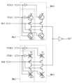
まず、遅延ブロック回路61について説明する。図8は、遅延ブロック回路の構成例を示す回路図である。遅延ブロック回路61は、2組のFINE遅延回路611e、611оと、COARSE遅延回路612と、コード制御回路613とを含む。First, the
FINE遅延回路611e、611оは、入力クロックINの立ち上がりのタイミングを、1.0Tw時間以下の分解能(具体的には、(1.0/(m×s))Tw時間単位)で補正する遅延回路である。FINE遅延回路611e、611оは、4つの入力端子CKIN_A、CKIN_B、FI_T、FI_Bと、1つの出力端子CKOUTを有する遅延回路である。The
図9は、FINE遅延回路の構成例を示す回路図である。FINE遅延回路611eは、2組のインバータ回路614a、614bを含む。インバータ回路614aは、(m×s)個のPサイドスイッチ71_1、71_2、…、71_(m×s)と、1個のNサイドスイッチ72とから構成される。図9は、s=2、m=4の場合を示している。Pサイドスイッチ71_εは、2個のPMOSトランジスタを直列に接続して構成される。以下、「ε」を含んだ表記は、εが1以上(m×s)以下の値の各々のケースの全てを一括して示すものとする。すなわち、「ε」を含んだ表記は、εが1のケース、εが2のケース、…、εが(m×s)のケースを一括して示すものとする。(m×s)個のPサイドスイッチ71_εは、インバータ回路614aの出力端子CKOUT_Tと電源電位Vccのノードとの間に、並列に接続される。Nサイドスイッチ72は、2個のNMOSトランジスタを直列に接続して構成される。Nサイドスイッチ72は、インバータ回路614aの出力端子CKOUT_Tと接地電位Vssのノードとの間に接続される。Figure 9 is a circuit diagram showing an example of the configuration of a FINE delay circuit. The
Pサイドスイッチ71_εを構成する2個のPMOSトランジスタのうち、ドレインがインバータ回路614aの出力端子CKOUT_Tに接続されている側のPMOSトランジスタ(以下、第1PMOSトランジスタと示す)のゲートは、入力端子CKIN_Aと接続されている。Pサイドスイッチ71_εを構成する他方のPMOSトランジスタ(以下、第2PMOSトランジスタと示す)のゲートには、入力端子FI_Tから入力される(m×s)ビットのコード信号のうち、設定された1ビットのデータが入力される。すなわち、出力端子CKOUT_Tに近いPサイドスイッチ71から順に、入力端子FI_Tから入力されるコード信号の1ビット目のデータ、2ビット目のデータ、…、(m×s)ビット目のデータ、が入力される。Of the two PMOS transistors constituting the P-side switch 71_ε, the gate of the PMOS transistor (hereinafter referred to as the first PMOS transistor) whose drain is connected to the output terminal CKOUT_T of the
図9に示す構成の場合、入力端子FI_Tから入力されるコード信号の1ビット目のデータはPサイドスイッチ71_8に入力され、同信号の2ビット目のデータはPサイドスイッチ71_7に入力され、同信号の3ビット目のデータはPサイドスイッチ71_6に入力され、同信号の4ビット目のデータはPサイドスイッチ71_5に入力される。さらに、同信号の5ビット目のデータはPサイドスイッチ71_4に入力され、同信号の6ビット目のデータはPサイドスイッチ71_3に入力され、同信号の7ビット目のデータはPサイドスイッチ71_2に入力され、同信号の8ビット目のデータはPサイドスイッチ71_1に入力される。具体的には、入力端子FI_Tから入力される8ビットのコード信号が"11100000"の場合、Pサイドスイッチ71_1、71_2、71_3のゲートには"1(=H)"が入力され、Pサイドスイッチ71_4、71_5、71_6、71_7、71_8の第2PMOSトランジスタのゲートには"0(=L)"が入力される。9, the first bit of data of the code signal input from input terminal FI_T is input to P-side switch 71_8, the second bit of data of the same signal is input to P-side switch 71_7, the third bit of data of the same signal is input to P-side switch 71_6, and the fourth bit of data of the same signal is input to P-side switch 71_5. Furthermore, the fifth bit of data of the same signal is input to P-side switch 71_4, the sixth bit of data of the same signal is input to P-side switch 71_3, the seventh bit of data of the same signal is input to P-side switch 71_2, and the eighth bit of data of the same signal is input to P-side switch 71_1. Specifically, when the 8-bit code signal input from the input terminal FI_T is "11100000", "1 (=H)" is input to the gates of the P-side switches 71_1, 71_2, and 71_3, and "0 (=L)" is input to the gates of the second PMOS transistors of the P-side switches 71_4, 71_5, 71_6, 71_7, and 71_8.
Nサイドスイッチ72を構成する2個のNMOSトランジスタのうち、ドレインがインバータ回路614aの出力端子CKOUT_Tに接続されている側のNMOSトランジスタ(以下、第1NMOSトランジスタと示す)のゲートは、入力端子CKIN_Aと接続されている。Nサイドスイッチ72を構成する他方のNMOSトランジスタ(以下、第2NMOSトランジスタと示す)のゲートは、入力端子CKIN_Bと接続されている。Of the two NMOS transistors constituting the N-
インバータ回路614bは、(m×s)個のPサイドスイッチ73_1、73_2、…、73_(m×s)と、1個のNサイドスイッチ74とから構成される。Pサイドスイッチ73_εは、2個のPMOSトランジスタを直列に接続して構成される。(m×s)個のPサイドスイッチ73_εは、インバータ回路614aの出力端子CKOUT_Bと電源電位Vccのノードとの間に、並列に接続される。なお、Pサイドスイッチ71_εと同様に、Pサイドスイッチ73_εを構成する2個のPMOSトランジスタのうち、ドレインがインバータ回路614bの出力端子CKOUT_Bに接続されている側のPMOSトランジスタを第1PMOSトランジスタと示し、他方のPMOSトランジスタを第2PMOSトランジスタと示す。Nサイドスイッチ74は、2個のNMOSトランジスタを直列に接続して構成される。Nサイドスイッチ74は、インバータ回路614bの出力端子CKOUT_Bと接地電位Vssのノードとの間に接続される。なお、Nサイドスイッチ72と同様に、Nサイドスイッチ74を構成する2個のNMOSトランジスタのうち、ドレインがインバータ回路614bの出力端子CKOUT_Bに接続されている側のNMOSトランジスタを第1NMOSトランジスタと示し、他方のNMOSトランジスタを第2NMOSトランジスタと示す。The
Pサイドスイッチ73_εを構成する2個のPMOSトランジスタのうち、第1PMOSトランジスタのゲートは入力端子CKIN_Bと接続されている。Pサイドスイッチ73_εの第2PMOSトランジスタのゲートには、入力端子FI_Bから入力される(m×s)ビットのコード信号のうち、設定された1ビットのデータが入力される。すなわち、出力端子CKOUT_Bに近いPサイドスイッチ73から順に、入力端子FI_Bから入力されるコード信号の1ビット目のデータ、2ビット目のデータ、…、(m×s)ビット目のデータ、が入力される。Of the two PMOS transistors constituting the P-side switch 73_ε, the gate of the first PMOS transistor is connected to the input terminal CKIN_B. The gate of the second PMOS transistor of the P-side switch 73_ε receives a set 1-bit data of the (m×s)-bit code signal input from the input terminal FI_B. That is, starting from the P-
図9に示す構成の場合、入力端子FI_Bから入力されるコード信号の1ビット目のデータはPサイドスイッチ73_8に入力され、同信号の2ビット目のデータはPサイドスイッチ73_7に入力され、同信号の3ビット目のデータはPサイドスイッチ73_6に入力され、同信号の4ビット目のデータはPサイドスイッチ73_5に入力される。さらに、同信号の5ビット目のデータはPサイドスイッチ73_4に入力され、同信号の6ビット目のデータはPサイドスイッチ73_3に入力され、同信号の7ビット目のデータはPサイドスイッチ73_2に入力され、同信号の8ビット目のデータはPサイドスイッチ73_1に入力される。具体的には、入力端子FI_Bから入力される8ビットのコード信号が"00011111"の場合、Pサイドスイッチ73_4、73_5、73_6、73_7、73_8、のゲートには"1(=H)"が入力され、Pサイドスイッチ73_1、73_2、73_3の第2PMOSトランジスタのゲートには"0(=L)"が入力される。9, the first bit of data of the code signal input from input terminal FI_B is input to P-side switch 73_8, the second bit of data of the same signal is input to P-side switch 73_7, the third bit of data of the same signal is input to P-side switch 73_6, and the fourth bit of data of the same signal is input to P-side switch 73_5. Furthermore, the fifth bit of data of the same signal is input to P-side switch 73_4, the sixth bit of data of the same signal is input to P-side switch 73_3, the seventh bit of data of the same signal is input to P-side switch 73_2, and the eighth bit of data of the same signal is input to P-side switch 73_1. Specifically, when the 8-bit code signal input from input terminal FI_B is "00011111", "1 (=H)" is input to the gates of P-side switches 73_4, 73_5, 73_6, 73_7, and 73_8, and "0 (=L)" is input to the gates of the second PMOS transistors of P-side switches 73_1, 73_2, and 73_3.
Nサイドスイッチ74を構成する2個のNMOSトランジスタのうち、第1NMOSトランジスタのゲートは、入力端子CKIN_Bと接続されている。Nサイドスイッチ72の第2NMOSトランジスタのゲートは、入力端子CKIN_Aと接続されている。Of the two NMOS transistors that make up the N-
インバータ回路614aの出力端子CKOUT_Tと、インバータ回路614bの出力端子CKOUT_Bとは、電気的に接続されている。すなわち、出力端子CKOUT_Tと出力端子CKOUT_Bとは、ショートされている。インバータ回路614aからの出力信号とインバータ回路614bからの出力信号がマージされた信号PI_CLKBは、インバータにより論理反転され、出力端子CKOUTから出力される。The output terminal CKOUT_T of the
FINE遅延回路611eは、入力端子CKIN_Aに入力クロックINの論理が反転された信号(クロックINB)が入力され、入力端子CKIN_BにクロックINBが1.0Tw時間遅延された信号(クロックINB1)が入力される。また、FINE遅延回路611eは、入力端子FI_Tに、コード信号DN_FDが入力される。さらに、入力端子FI_Bに、コード信号DN_FDが論理反転された信号であるコード信号DN_FDBが入力される。The
FINE遅延回路611eは、クロックINB、クロックINB1と、コード信号DN_FDと、コード信号DN_FDBとを受け取り、クロックFOUTB_EVNを生成する。クロックFOUTB_EVNは、入力クロックINの立ち上がりを、コード信号DN_FD、DN_FDBに基づき0~1.0TWの範囲で遅延させ、論理反転させた信号である。The
FINE遅延回路611оは、入力端子CKIN_Bに入力クロックINの論理が反転された信号(クロックINB)が入力され、入力端子CKIN_AにクロックINBが1.0Tw時間遅延された信号(クロックINB1)が入力される。また、FINE遅延回路611eは、入力端子FI_Tに、コード信号DN_FDが入力される。さらに、入力端子FI_Bに、コード信号DN_FDが論理反転された信号であるコード信号DN_FDBが入力される。The FINE delay circuit 611o receives a signal (clock INB) that is the logically inverted version of the input clock IN at its input terminal CKIN_B, and receives a signal (clock INB1) that is the clock INB delayed by 1.0 Tw at its input terminal CKIN_A. The
FINE遅延回路611oは、クロックINB、クロックINB1と、コード信号DN_FDと、コード信号DN_FDBとを受け取り、クロックFOUTB_ODDを生成する。クロックFOUTB_ODDは、入力クロックINの立ち上がりを、コード信号DN_FD、DN_FDBに基づき0~1.0TWの範囲で遅延させ、論理反転させた信号である。なお、FINE遅延回路611e、611оにおけるクロックFOUTB_EVN、FOUTB_ODDの生成については、後に詳述する。The FINE delay circuit 611o receives the clocks INB, INB1, the code signals DN_FD, and DN_FDB, and generates the clock FOUTB_ODD. The clock FOUTB_ODD is a signal that is generated by delaying the rising edge of the input clock IN in the range of 0 to 1.0 TW based on the code signals DN_FD and DN_FDB, and then logically inverting the signal. The generation of the clocks FOUTB_EVN and FOUTB_ODD in the
コード制御回路613は、コード信号DN_C、DN_Fを受け取り、FINE遅延回路611eの入力端子FI_T、及び、FINE遅延回路611оの入力端子FI_Tに入力するコード信号DN_FDを生成する。コード信号DN_FDは、(m×s)ビットの温度計コードである。コード制御回路613におけるコード信号DN_FDの生成については、後に詳述する。The
COARSE遅延回路612は、入力クロックINの立ち上がりのタイミングを、1.0Tw時間単位で補正する遅延回路である。COARSE遅延回路612は、信号FOUTE_EVNと、信号FOUTE_ODDと、コード信号DN_Cとを受け取り、コード信号DN_Cに基づき、クロックFOUTB_EVN、クロックFOUTB_ODDのいずれか一方を、コード信号DN_Cに基づく量だけ選択した信号を遅延させ、遅延させた信号を出力クロックCDLYOUTとして出力する。The
COARSE遅延回路612は、l+1個の遅延要素615_0~615_lを含む。遅延要素615_0~615_lは、出力端に近い側から、遅延要素615_0、615_1、615_2、…、615_lの順に配置されている。γ(γは0、及び、1以上l以下の自然数)が0~lの各々のケースにおいて、遅延要素615_γは、例えば、3つのNANDゲートを含む。以下、「γ」を含んだ表記は、γが0以上l以下の値の各々のケースの全てを一括して示すものとする。すなわち、「γ」を含んだ表記は、γが0のケース、γが1のケース、…、γがlのケースを一括して示すものとする。遅延要素615_γは、時間1.0Twだけの遅延を生じさせる。The
また、COARSE遅延回路612は、コード変換回路616を含む。コード変換回路616は、演算回路42から出力された信号DCA_CODEに含まれるコード信号DN_Cを受け取ってデコードし、バイナリコードを温度計コードに変換し、コード信号DN_CDを生成する。コード信号DN_CDは、lビットのコード信号である。例えば、コード信号DN_Cとして十進数の"4"を示すバイナリコード"100"を受け取った場合、コード変換回路616は、コード信号DN_CDとして"0…01111"を生成する。すなわち、コード変換回路616は、1ビット目からコード信号DN_Cが示す数のビットまでを"1"とし、他のビットを"0"とするコード信号DN_CDを生成する。コード変換回路616は、生成したコード信号DN_CDを、遅延要素615に出力する。The
遅延要素615_γの第1のNANDゲートは、1つの入力において、クロックFOUTB_EVN、クロックFOUTB_ODDのいずれか一方を受け取る。具体的には、γが偶数の場合、クロックFOUTB_EVNを受け取り、γが奇数の場合、クロックFOUTB_ODDを受け取る。また、第1のNANDゲートは、もう1つの入力において、コード信号DN_CDγ(コード信号DN_CDのγビット目の値)を受け取る。ただし、遅延要素615_0においては、第1のNANDゲートは、もう1つの入力において、電源電位Vccのノードに接続されている。The first NAND gate of delay element 615_γ receives either the clock FOUTB_EVN or the clock FOUTB_ODD at one input. Specifically, when γ is an even number, it receives the clock FOUTB_EVN, and when γ is an odd number, it receives the clock FOUTB_ODD. The first NAND gate also receives the code signal DN_CDγ (the value of the γth bit of the code signal DN_CD) at the other input. However, in delay element 615_0, the first NAND gate has the other input connected to a node of the power supply potential Vcc.
遅延要素615_γの第2のNANDゲートは、1つの入力において、遅延要素615_(γ+1)から出力される信号FOUTB_(γ+1)を受け取る。また、第2のNANDゲートは、もう1つの入力において、電源電位Vccのノードに接続されている。ただし、遅延要素615_nの第2のNANDゲートは、2つの入力において接地されており、すなわち、接地電位Vssのノードに接続されている。The second NAND gate of delay element 615_γ receives the signal FOUTB_(γ+1) output from delay element 615_(γ+1) at one input. The second NAND gate also has another input connected to a node of power supply potential Vcc. However, the second NAND gate of delay element 615_n has two inputs grounded, i.e., connected to a node of ground potential Vss.
遅延要素615_γの第3のNANDゲートは、第1のNANDゲートの出力と、第2のNANDゲートの出力とを受け取り、信号FOUTB_γを出力する。The third NAND gate of delay element 615_γ receives the output of the first NAND gate and the output of the second NAND gate, and outputs signal FOUTB_γ.
遅延要素615_γは、第1のNANDゲートに入力される、コード信号DN_CDγの値が"0(=L)"である場合、信号FOUTB_γとして"0(=L)"を出力する。一方、第1のNANDゲートに入力される、コード信号DN_CDγの値が"1(=H)"であり、コード信号DN_CD(γ+1)の値が"0(=L)"である場合、信号FOUTB_γとして、第1のNANDゲートに入力される信号FOUTB_ODDもしくはFOUTB_EVNが時間1.0Twだけ遅延された信号を出力する。コード信号DN_CDγの値が"1(=H)"であり、コード信号DN_CD(γ+1)の値が"1(=H)"である場合、信号FOUTB_γとして、第2のNANDゲートに入力される信号FOUTB_(γ+1)が時間1.0Twだけ遅延された信号を出力する。遅延要素615_0から出力された信号FOUTB_0は、出力クロックCDLYOUTとしてCOARSE遅延回路612から出力される。When the value of the code signal DN_CDγ input to the first NAND gate is "0 (=L)", the delay element 615_γ outputs "0 (=L)" as the signal FOUTB_γ. On the other hand, when the value of the code signal DN_CDγ input to the first NAND gate is "1 (=H)" and the value of the code signal DN_CD(γ+1) is "0 (=L)", the delay element 615_γ outputs, as the signal FOUTB_γ, a signal that is a delayed version of the signal FOUTB_ODD or FOUTB_EVN input to the first NAND gate by a time of 1.0Tw. When the value of the code signal DN_CDγ is "1 (=H)" and the value of the code signal DN_CD(γ+1) is "1 (=H)", the signal FOUTB_γ is output, which is a signal that is a delay of the signal FOUTB_(γ+1) input to the second NAND gate by a time of 1.0Tw. The signal FOUTB_0 output from the delay element 615_0 is output from the
出力クロックCDLYOUTは、インバータにより論理反転され、遅延クロックCDLY_Tとして遅延ブロック回路61から出力される。The output clock CDLYOUT is logically inverted by an inverter and output from the
遅延ブロック回路62は、上述した遅延ブロック回路61と同様の構成である。ただし、入出力信号が、遅延ブロック回路61とは異なる。すなわち、遅延ブロック回路61では、入力クロックINと、信号DCA_CODEを構成するコード信号DN_F、DN_Cを受け取り、遅延クロックCDLY_Tを生成するのに対し、遅延ブロック回路62では、入力クロック/INと、信号DCA_CODEを構成するコード信号UP_F、UP_Cを受け取り、遅延クロックCDLY_Bを生成する。The
波形生成回路44は、遅延クロックCDLY_Tの立ち上がり(立ち上がりエッジ)から遅延クロックCDLY_Bの立ち上がり(立ち上がりエッジ)までの期間にわたってハイレベルを維持する出力クロックOUTを生成する回路である。波形生成回路44は、例えば、遅延クロックCDLY_T、及び、遅延クロックCDLY_Bの2つの信号を入力とし、出力クロックOUTを出力とする、2入力1出力のマルチプレクサ(遅延クロックCDLY_Tと、遅延クロックCDLY_Bの反転信号との論理積を出力するマルチプレクサ)として構成される。
(1-3-4.波形生成回路の構成)
図10は、波形生成回路の構成例を示すブロック図である。実施形態の波形生成回路44は、インバータINV1と、複数のインバータが直列に接続されたインバータ群INVG1、INVG2と、PMOSトランジスタP1、P2と、NMOSトランジスタN1、N2と、ラッチ回路LAT1とから構成されている。 The
(1-3-4. Configuration of the Waveform Generation Circuit)
10 is a block diagram showing an example of the configuration of a
PMOSトランジスタP2、P1、及び、NMOSトランジスタN1、N2は直列接続されている。PMOSトランジスタP2のソースは電源電位Vccに接続されており、NMOSトランジスタN2のソースは接地電位Vssに接続されている。遅延クロックCDLY_Bは、インバータIN1を介して論理反転され、PMOSトランジスタP1のゲートと、インバータ群INVG1に入力される。インバータ群INVG1の出力は、PMOSトランジスタP2のゲートに入力される。遅延クロックCDLY_Tは、NMOSトランジスタN2のゲート電極と、インバータ群INVG2に入力される。インバータ群INVG2の出力は、NMOSトランジスタN2のゲートに入力される。The PMOS transistors P2 and P1 and the NMOS transistors N1 and N2 are connected in series. The source of the PMOS transistor P2 is connected to the power supply potential Vcc, and the source of the NMOS transistor N2 is connected to the ground potential Vss. The delayed clock CDLY_B is logically inverted via the inverter IN1 and input to the gate of the PMOS transistor P1 and the inverter group INVG1. The output of the inverter group INVG1 is input to the gate of the PMOS transistor P2. The delayed clock CDLY_T is input to the gate electrode of the NMOS transistor N2 and the inverter group INVG2. The output of the inverter group INVG2 is input to the gate of the NMOS transistor N2.
PMOSトランジスタP1のドレインとNMOSトランジスタN2のドレインの接続点は、ラッチ回路LAT1の入力に接続されている。ラッチ回路LAT2は、2つのインバータを正帰還させた構成を有する。The connection point between the drain of the PMOS transistor P1 and the drain of the NMOS transistor N2 is connected to the input of the latch circuit LAT1. The latch circuit LAT2 has a configuration in which two inverters are positively fed back.
波形生成回路44に入力された遅延クロックCDLY_Bがローレベルからハイレベルに切り替わると、PMOSトランジスタP1、P2がONになり、電源電位Vccがラッチ回路LAT1に入力される。一方、波形生成回路44に入力された遅延クロックCDLY_Tがローレベルからハイレベルに切り替わると、NMOSトランジスタN1、N2がONになり、接地電位Vssがラッチ回路LAT1に入力される。従って、ラッチ回路LAT1から出力される信号(=出力クロックOUT)は、遅延クロックCDLY_Tの立ち上がりエッジにおいてローレベルからハイレベルに切り替わり、遅延クロックCDLY_Bの立ち上がりエッジにおいて、ハイレベルからローレベルに切り替わる、クロック信号となる。When the delayed clock CDLY_B input to the
波形生成回路44は、ラッチ回路LAT1から出力される信号を、出力クロックOUTとして出力する。また、出力クロックOUTの論理を反転した信号(出力クロック/OUT)も生成し、出力する。なお、出力クロックOUT、/OUTは、DCC回路20から出力されるとともに、DCD回路41に入力される。出力クロックOUTは、入力クロックDCD_INとしてDCD回路41に入力され、出力クロック/OUTは、入力クロック/DCD_INとしてDCD回路41に入力される。
(2.動作)
(2-1.DCC回路の動作)
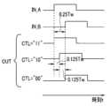
図11は、DCC回路の動作の一例を説明するタイミングチャートである。図11に示すように、DCC回路20に入力される入力クロックINは、あるデューティーサイクルを有する。例えば、デューティーサイクルは50%でなく、ハイレベル期間(期間CINH)がローレベル期間(期間CINL)よりも短い。入力クロックINは、周期CINを有し、期間CINHに亘ってハイレベルであり、期間CINLに亘ってローレベルである。すなわち、入力クロックINは、CIN=CINH+CINL、CINH<CINLの関係を有する。 The
2. Operation
(2-1. Operation of DCC Circuit)
11 is a timing chart for explaining an example of the operation of the DCC circuit. As shown in FIG. 11, the input clock IN input to the
DCC回路20に入力された入力クロックINは、DCD回路41において、最初の数サイクル(例えば、12サイクル)でデューティーが検出される。具体的な検出方法について以下に述べる。まず、入力クロックDCD_INの1サイクル目において、エッジ検出回路53のセレクタ56は、遅延素子551から出力される信号CLK_DETa1を選択し信号CLK_DETaとして出力するように設定される。DCD回路41は、入力クロックDCD_INの1サイクル目のパルス幅(ハイレベルの期間)を計測し、信号DCD_CODEを生成して演算回路42へ出力する。また、DCD回路41は、入力クロック/DCD_INの4サイクル目のパルス幅を計測し、信号DCD_CODEを生成して演算回路42へ出力する。The input clock IN input to the
入力クロック/DCD_INの7サイクル目において、エッジ検出回路53のセレクタ56は、遅延素子551から出力される信号CLK_DETa2を選択し信号CLK_DETaとして出力するように切り替られる。DCD回路41は、入力クロックDCD_INの8サイクル目のパルス幅(ハイレベルの期間)を計測し、信号DCD_CODEを生成して演算回路42へ出力する。また、DCD回路41は、入力クロック/DCD_INの11サイクル目のパルス幅を計測し、信号DCD_CODEを生成して演算回路42へ出力する。In the seventh cycle of the input clock /DCD_IN, the
すなわち、セレクタ56において、出力する信号CLK_DETaを切り替える都度、入力クロックDCD_INのハイレベルの期間と、入力クロック/DCD_INのハイレベルの期間とを計測し、信号DCD_CODEを生成して演算回路42へ出力する。入力クロックDCD_INのハイレベルの期間の計測と、入力クロック/DCD_INのハイレベルの期間の計測とを1セットとすると、sセット分の計測が実行される。That is, each time the
なお、入力クロックIN、/INのデューティー補正がなされる以前のサイクルにおいて、出力クロックOUT、/OUTは入力クロックIN、/INとデューティーが等しい。従って、入力クロックDCD_IN、/DCD_INのデューティーは、入力クロックIN、/INのデューティーと等しい。すなわち、DCC回路20から出力される信号DCD_CODEは、各セットにおいて、入力クロックINの1サイクル目の立ち下がり(=入力クロック/INの1サイクル目の立ち上がり)から入力クロック/INの4サイクル目の立ち下がり(=入力クロックINの5サイクル目の立ち上がり)までの期間は、クロックINの1サイクル目のパルス幅の検出結果に基づいて生成された値であり、入力クロック/INの4サイクル目の立ち下がり(=入力クロックINの5サイクル目の立ち上がり)から入力クロックINの8サイクル目の立ち下がり(=入力クロック/INの8サイクル目の立ち上がり)までの期間は、入力クロック/INの4サイクル目のパルス幅の検出結果に基づいて生成された値である。In the cycle before the duty correction of the input clocks IN and /IN is performed, the output clocks OUT and /OUT have the same duty as the input clocks IN and /IN. Therefore, the duty of the input clocks DCD_IN and /DCD_IN is equal to the duty of the input clocks IN and /IN. That is, the signal DCD_CODE output from the
すなわち、DCC回路20から出力される信号DCD_CODEは、「信号CLK_DETa1を用いて計測した入力クロックDCD_INのハイレベルの期間(=1セット目における入力クロックDCD_INのハイレベルの期間)」「信号CLK_DETa1を用いて計測した入力クロック/DCD_INのハイレベルの期間(=1セット目における入力クロック/DCD_INのハイレベルの期間)」「信号CLK_DETa2を用いて計測した入力クロックDCD_INのハイレベルの期間(=2セット目における入力クロックDCD_INのハイレベルの期間)」「信号CLK_DETa2を用いて計測した入力クロック/DCD_INのハイレベルの期間(=2セット目における入力クロック/DCD_INのハイレベルの期間)」の順に出力される。That is, the signal DCD_CODE output from the
演算回路42は、信号DCD_CODEにより、信号CLK_DETa1を用いて計測した入力クロックINのパルス幅の検出結果と、信号CLK_DETa2を用いて計測した入力クロックINのパルス幅の検出結果とを受け取ると、これらを用いて入力クロックINのパルス幅を算出する。また、信号DCD_CODEにより、信号CLK_DETa1を用いて計測した入力クロック/INのパルス幅の検出結果と、信号CLK_DETa2を用いて計測した入力クロック/INのパルス幅の検出結果とを受け取ると、これらを用いて入力クロック/INのパルス幅を算出する。続いて、算出された入力クロックINのパルス幅と、算出された入力クロック/INのパルス幅とを比較する。そして、比較結果に基づいて、信号DCA_CODEを生成する。例えば上述のように、入力クロックINの12サイクル目の立ち上がりから信号CLK_DETa2を用いて計測した入力クロック/INのパルス幅の検出結果を受け取る場合、入力クロックINの12サイクル目の間に信号DCA_CODEを生成して出力する。When the
そして、DCA回路43と波形生成回路44において、信号DCA_CODEに基づいて入力クロックIN、/INのデューティーが補正され、出力クロックOUT、/OUTとしてDCC回路20から出力される。なお、信号DCA_CODEが生成される前のサイクル(1~12サイクル目)については、入力クロックIN、/INが補正されずに出力クロックOUT、/OUTとなる。入力クロックINの12サイクル目の間に受け取った信号DCA_CODEに基づいて、入力クロックINのデューティーを補正する。そして、出力クロックOUTの13サイクル目からは、補正後のクロック信号DCC回路20から出力される。Then, in the
出力クロックOUT、/OUTは、それぞれ入力クロックDCD_IN、/DCD_INとしてDCD回路41にフィードバックされる。DCD回路41は、設定された適切な間隔で、入力クロックDCD_INのパルス幅と、入力クロック/DCD_INのパルス幅とを計測し、信号DCD_CODEを更新する。演算回路42は、信号DCD_CODEが更新されると、信号DCA_CODEを更新する。そして、DCA回路43と波形生成回路44において、更新された信号DCA_CODEに基づいて入力クロックIN、/INのデューティーが補正され、出力クロックOUT、/OUTとしてDCC回路20から出力される。The output clocks OUT and /OUT are fed back to the
このように、本実施形態によれば、入力クロックIN、/INのデューティー補正後も、出力クロックOUT、/OUTをDCD回路41にフィードバックしてモニタを続け、信号DCD_CODEを更新し続ける。これにより、半導体記憶装置2が動作中における温度や電圧の変動により、入力クロックIN、/INのデューティーに変化が生じた場合にも、これらの変動に追従して、デューティーを適切に補正することができる。また、信号DCD_CODEを検出する際に、ノイズなどの外乱により一時的に誤差が生じる場合にも、継続的に信号DCD_CODEを検出することにより、信号DCD_CODEの検出回数を増加させ、誤差を平均化して影響を低減することができる。さらに、DCD回路41に設けられている遅延要素521_αと、DCA回路43に設けられている遅延要素615_γの特性差分に起因する誤差を解消することができる。
(2-1-1.DCD回路の動作)
図12、図13A、及び、図13Bは、DCD回路の動作の一例を説明するタイミングチャートである。DCD回路41には、入力クロックDCD_IN、/DCD_INが入力される。信号生成回路51は、各セットにおいて、入力クロックDCD_INの最初のサイクルの立ち上がりを検出し、この立ち上がりから入力クロックDCD_INの次のサイクルの立ち上がりまでの期間と同じ期間に亘って信号CLK_DLYをハイレベルに維持する。また、信号生成回路51は、各セットにおいて、入力クロック/DCD_INの4サイクル目の立ち上がり(=入力クロックDCD_INの4サイクル目の立ち下がり)を検出し、この立ち上がりから入力クロック/CLK_DLYの次のサイクルの立ち上がりまでの期間と同じ期間に亘って信号CLK_DLYをハイレベルに維持する。 In this way, according to the present embodiment, even after the duty correction of the input clocks IN and /IN, the output clocks OUT and /OUT are fed back to the
(2-1-1. Operation of DCD Circuit)
12, 13A, and 13B are timing charts for explaining an example of the operation of the DCD circuit. Input clocks DCD_IN and /DCD_IN are input to the
すなわち、信号生成回路51は、1セット目において、入力クロックDCD_INの1サイクル目の立ち上がりを検出し、この立ち上がりから入力クロックDCD_INの次のサイクルの立ち上がりまでの期間と同じ期間に亘って信号CLK_DLYをハイレベルに維持する。また、信号生成回路51は、入力クロック/DCD_INの4サイクル目の立ち上がり(=入力クロックDCD_INの4サイクル目の立ち下がり)を検出し、この立ち上がりから入力クロック/DCD_INの次のサイクルの立ち上がりまでの期間と同じ期間に亘って信号CLK_DLYをハイレベルに維持する。That is, in the first set, the
さらに、信号生成回路51は、エッジ検出回路53のセレクタ56が切り替えられ、信号CLK_DETaとして出力される信号が変更された後、すなわち2セット目に切り替わった後の最初のサイクルである8サイクル目の立ち上がりを検出し、この立ち上がりから入力クロックDCD_INの次のサイクルの立ち上がりまでの期間と同じ期間に亘って信号CLK_DLYをハイレベルに維持する。また、信号生成回路51は、2セット目の入力クロック/DCD_INの4サイクル目、すなわち、入力クロック/DCD_INの11サイクル目の立ち上がり(=入力クロックDCD_INの11サイクル目の立ち下がり)を検出し、この立ち上がりから入力クロック/CLK_DLYの次のサイクルの立ち上がりまでの期間と同じ期間に亘って信号CLK_DLYをハイレベルに維持する。Furthermore, the
信号生成回路51は、各セットにおいて、入力クロックDCD_INの最初のサイクルの立ち下がりを検出し、この立ち下がりから入力クロックDCD_INの次のサイクルの立ち下がりまでの期間と同じ期間に亘って信号CLK_DETをハイレベルに維持する。また、信号生成回路51は、入力クロック/DCD_INの4サイクル目の立ち下がり(=入力クロックDCD_INの5サイクル目の立ち上がり)を検出し、この立ち下がりから入力クロック/DCD_INの次のサイクルの立ち下がりまでの期間と同じ期間に亘って信号CLK_DETをハイレベルに維持する。In each set, the
すなわち、信号生成回路51は、1セット目において、入力クロックDCD_INの最初のサイクルの立ち下がりを検出し、この立ち下がりから入力クロックDCD_INの次のサイクルの立ち下がりまでの期間と同じ期間に亘って信号CLK_DETをハイレベルに維持する。また、信号生成回路51は、入力クロック/DCD_INの4サイクル目の立ち下がり(=入力クロックDCD_INの5サイクル目の立ち上がり)を検出し、この立ち下がりから入力クロック/DCD_INの次のサイクルの立ち下がりまでの期間と同じ期間に亘って信号CLK_DETをハイレベルに維持する。That is, in the first set, the
さらに、信号生成回路51は、エッジ検出回路53のセレクタ56が切り替えられ、信号CLK_DETaとして出力される信号が変更された後、すなわち2セット目に切り替わった後の最初のサイクルである入力クロックDCD_INの最初のサイクル(=8サイクル目)の立ち下がりを検出し、この立ち下がりから入力クロックDCD_INの次のサイクルの立ち下がりまでの期間と同じ期間に亘って信号CLK_DETをハイレベルに維持する。また、信号生成回路51は、2セット目の入力クロック/DCD_INの4サイクル目である入力クロック/DCD_INの11サイクル目の立ち下がり(=入力クロックDCD_INの12サイクル目の立ち上がり)を検出し、この立ち下がりから入力クロック/DCD_INの次のサイクルの立ち下がりまでの期間と同じ期間に亘って信号CLK_DETをハイレベルに維持する。Furthermore, the
なお、信号生成回路51は、定められたタイミングの都度、あるいは、デューティーの調整が要求される都度、信号CLK_DLY、CLK_DETについて、上述の動作を繰り返す。すなわち、信号CLK_DLYの奇数サイクルにおけるハイレベルの期間は、入力クロックCLK_INの1サイクルと同じ長さであり、偶数サイクルにおけるハイレベルの期間は、入力クロック/CLK_INの1サイクルと同じ長さである。また、信号CLK_DETの奇数サイクルにおけるハイレベルの期間は、入力クロックCLK_INの1サイクルと同じ長さであり、偶数サイクルにおけるハイレベルの期間は、入力クロック/CLK_INの1サイクルと同じ長さである。The
上述のように生成された信号CLK_DLYと信号CLK_DETにおいては、信号CLK_DLYの奇数サイクルの立ち上がりから、信号CLK_DETの立ち上がりまでの期間は、入力クロックDCD_INのパルス幅と同じ期間である。また、信号CLK_DLYの偶数サイクルの立ち上がりから、信号CLK_DETの立ち上がりまでの期間は、入力クロック/DCD_INのパルス幅と同じ期間である。In the signals CLK_DLY and CLK_DET generated as described above, the period from the rising edge of the odd cycle of the signal CLK_DLY to the rising edge of the signal CLK_DET is the same as the pulse width of the input clock DCD_IN. Also, the period from the rising edge of the even cycle of the signal CLK_DLY to the rising edge of the signal CLK_DET is the same as the pulse width of the input clock DCD_IN.
遅延素子アレイ回路52は、信号生成回路51から受け取った信号CLK_DLYを信号D0とし、信号D0に基づき各遅延素子521_αにおいて信号Dαを生成し出力する。すなわち、遅延素子521_αは、信号D(α―1)が時間Twだけ遅延された信号を信号Dαとして出力する。こうして、αの値が昇順に、時間Twだけ遅延された信号D1~Dnが得られる。図13Aは、信号D1~信号D(k+1)(kはn-1以下の自然数)の一部の信号を示している。The delay
エッジ検出回路53の遅延ライン53βには、クロック信号CLK_DETaが時間{1.0+(β-1)/m}×Twだけ遅延された信号が、クロック信号DLK_DETβとして供給される。A signal that is the clock signal CLK_DETa delayed by a time {1.0+(β-1)/m}×Tw is supplied to the delay line 53β of the
例えば、図6に示すように、エッジ検出回路53に4本の遅延ライン(m=4)が設けられている場合、遅延ライン531には、クロック信号CLK_DETaを時間1.0Twだけ遅延させた信号(クロック信号CLK_DET1)が供給される。同様に、遅延ライン532には、クロック信号CLK_DETを時間1.25Twだけ遅延させた信号(クロック信号CLK_DET2)が供給され、遅延ライン533には、クロック信号CLK_DETを時間1.5Twだけ遅延させた信号(クロック信号CLK_DET3)が供給される。また、遅延ライン534には、クロック信号CLK_DETを時間1.75Twだけ遅延させた信号(クロック信号CLK_DET4)が供給される。For example, as shown in FIG. 6, when the
遅延ライン53βに設けられたフリップフロップ53β_αは、クロック信号CLK_DETβのハイレベルへの移行に応答して信号Dαをラッチし、ラッチされた信号Dαを信号Fβαとして出力する。Flip-flop 53β_α provided in delay line 53β latches signal Dα in response to the transition of clock signal CLK_DETβ to high level, and outputs the latched signal Dα as signal Fβα.
例えば、図13Aに示すように、遅延ライン531において、クロック信号CLK_DET1がハイレベルに切り替わるタイミングにおいて、信号D1~D(k-1)がハイレベルであり、信号Dk~Dnはローレベルである場合、フリップフロップ531_1~531_(k-1)からは、信号F11~F1(k-1)としてハイレベルの信号が出力され、フリップフロップ531_k~531_nからは、信号F1k~F1nとしてローレベルの信号が出力される。For example, as shown in FIG. 13A, in the
遅延ライン532において、クロック信号CLK_DET2がハイレベルに切り替わるタイミングにおいて、信号D1~D(k-1)がハイレベルであり、信号Dk~Dnはローレベルである場合、フリップフロップ532_1~532_(k-1)からは、信号F21~F2(k-1)としてハイレベルの信号が出力される。フリップフロップ532_k~532_nからは、信号F2k~F2nとしてローレベルの信号が出力される。In the
遅延ライン533において、クロック信号CLK_DET3がハイレベルに切り替わるタイミングにおいて、信号D1~D(k-1)がハイレベルであり、信号Dk~Dnはローレベルである場合、図には示されていないが、フリップフロップ533_1~533_(k-1)からは、信号F31~F3(k-1)としてハイレベルの信号が出力される。フリップフロップ533_k~533_nからは、信号F3k~F3nとしてローレベルの信号が出力される。In the
遅延ライン534において、クロック信号CLK_DET4がハイレベルに切り替わるタイミングにおいて、信号D1~Dkがハイレベルであり、信号D(k+1)~Dnはローレベルである場合、フリップフロップ5343_1~534_kからは、信号F41~F4kとしてハイレベルの信号が出力される。フリップフロップ534_(k+1)~534_nからは、図には示されていないが、信号F4(k+1)~F4nとしてローレベルの信号が出力される。In the
遅延ライン53βから出力される信号Fβαは、信号DCD_CODEとして出力される。The signal Fβα output from delay line 53β is output as signal DCD_CODE.
ここで、図13Bに示すように、1セット目におけるクロック信号CLK_DETa(クロック信号CLK_DETa1)に対し、2セット目におけるクロック信号CLK_DETa(=クロック信号CLK_DETa2)は、{1/(m×s)}×Twだけ遅延されている。従って、1セット目におけるクロック信号DLK_DETβより、2セット目におけるクロック信号DLK_DETβは、{1/(m×s)}×Twだけ遅延されている。例えば、n=8、k=5の場合、1セット目のクロック信号CLK_DETa(クロック信号CLK_DETa1)では、図13Aに示すタイミングチャートに従って得られる信号Fβαは、以下のようになる。すなわち、信号F1n~信号F11は"00001111"、信号F2n~信号21は"00001111"、信号F3n~信号F31は"00001111"、信号F4n~信号F41の"00011111"の8ビット×4=32ビットの信号が得られる。エッジ検出回路53は、信号Fβαを順に並べて32ビット(=n×mビット)の信号DCD_CODEを生成し、出力する。例えば、上述の場合、信号DCD_CODEは、"00001111000011110000111100011111"となる。Here, as shown in FIG. 13B, the clock signal CLK_DETa (=clock signal CLK_DETa2) in the second set is delayed by {1/(m×s)}×Tw relative to the clock signal CLK_DETa (clock signal CLK_DETa1) in the first set. Therefore, the clock signal DLK_DETβ in the second set is delayed by {1/(m×s)}×Tw from the clock signal DLK_DETβ in the first set. For example, when n=8 and k=5, the signal Fβα obtained according to the timing chart shown in FIG. 13A for the clock signal CLK_DETa (clock signal CLK_DETa1) of the first set is as follows: That is, signals F1n to F11 are "00001111", signals F2n to F21 are "00001111", signals F3n to F31 are "00001111", and signals F4n to F41 are "00011111", resulting in a signal of 8 bits x 4 = 32 bits. The
2セット目のクロック信号CLK_DETa(クロック信号CLK_DETa2)では、図13Aに示すタイミングチャートに従って得られる信号Fβαは、以下のようになる。すなわち、信号F1n~信号F11は"00001111"、信号F2n~信号21は"00001111"、信号F3n~信号F31は"00011111"、信号F4n~信号F41の"00011111"の8ビット×4=32ビットの信号が得られる。つまり、1セット目に対して2セット目はクロック信号CLK_DETaが{1/(m×s)}×Twだけ遅延されているため、信号F34が"0"から"1"に変化している。エッジ検出回路53は、信号Fβαを順に並べて32ビット(=n×mビット)の信号DCD_CODEを生成し、出力する。例えば、上述の場合、信号DCD_CODEは、"00001111000011110001111100011111"となる。
(2-1-2.演算回路の動作)
演算回路42は、各セットにおけるクロック信号CLK_DETの最初のサイクルにおいて、DCD回路41から受け取った信号DCD_CODEのハイレベルのビット数(iδ)を計数する。例えば、1セット目における信号DCD_CODEが"00001111000011110000111100011111"の場合、ハイレベルのビット数は「i1=17」と計数される。また、2セット目における信号DCD_CODEが"00001111000011110001111100011111"の場合、ハイレベルのビット数は「i2=18」と計数される。 In the second set of clock signal CLK_DETa (clock signal CLK_DETa2), the signal Fβα obtained according to the timing chart shown in FIG. 13A is as follows. That is, the signals F1n to F11 are "00001111", the signals F2n to F21 are "00001111", the signals F3n to F31 are "00011111", and the signals F4n to F41 are "00011111", resulting in a signal of 8 bits x 4 = 32 bits. That is, since the clock signal CLK_DETa in the second set is delayed by {1/(m x s)} x Tw compared to the first set, the signal F34 changes from "0" to "1". The
(2-1-2. Operation of the Arithmetic Circuit)
The
演算回路42は、各セットにおけるクロック信号CLK_DETの次のサイクルにおいて、DCD回路41から受け取った信号DCD_CODEのハイレベルのビット数(jδ)を計数する。例えば、1セット目の信号DCD_CODEが"01111111111111111111111111111111"の場合、ハイレベルのビット数は「j1=31」と計数される。また、2セット目における信号DCD_CODEが"01111111111111111111111111111111"の場合、ハイレベルのビット数は「j2=31」と計数される。The
数iは、入力クロックINのパルス幅(ハイレベルの期間)を表現する。具体的には、各セットの数ikの平均値をmで除した値と遅延時間Twとの積が、入力クロックINのハイレベルの幅を表現する。例えば、s=2、m=4、i1=17、i2=18の場合、入力クロックINのハイレベルの幅は、{(17+18)/2}/4×Tw=4.375Twとなる。The number i represents the pulse width (high level period) of the input clock IN. Specifically, the product of the average value of the numbers ik of each set divided by m and the delay time Tw represents the high level width of the input clock IN. For example, if s = 2, m = 4, i1 = 17, and i2 = 18, the high level width of the input clock IN is {(17 + 18) / 2} / 4 x Tw = 4.375 Tw.
数jは、入力クロック/INのパルス幅(ハイレベルの期間)を表現する。具体的には、各セットの数jkの平均値をmで除した値と遅延時間Twとの積が、入力クロック/INのハイレベルの幅を表現する。入力クロック/INのハイレベルの幅は、入力クロックINのローレベルの幅と等しい。ゆえに、数jは、入力クロックINのローレベルの幅を表現する。例えば、s=2、m=4、j1=31、j2=31の場合、入力クロックINのローレベルの幅は、{(31+31)/2}/4×Tw=7.75Twとなる。The number j represents the pulse width (high level period) of the input clock /IN. Specifically, the product of the average value of the numbers jk of each set divided by m and the delay time Tw represents the high level width of the input clock /IN. The high level width of the input clock /IN is equal to the low level width of the input clock IN. Therefore, the number j represents the low level width of the input clock IN. For example, if s = 2, m = 4, j1 = 31, and j2 = 31, the low level width of the input clock IN is {(31 + 31) / 2} / 4 x Tw = 7.75 Tw.
図14は、演算回路の動作を説明するフローチャートである。まず、演算回路42は、数i、数jの計算に用いる各種変数を初期設定する(S1)。具体的には、クロック信号CLK_DETのサイクル数をあらわす変数kに1をセットし、数ikの積算値を格納する変数isumに0をセットし、数jkの積算値を格納する変数jsumに0をセットする。演算回路42は、クロック信号CLK_DETの最初のサイクルにおいて、信号DCD_CODEのハイレベルのビット数を計数し、計数結果である数ikを取得する。(S2)。演算回路42は、数ikの積算値isumにS2で取得した数ikを足し合わせ、サイクル数kを1つインクリメントした後(S3)、クロック信号CLK_DETの次のサイクルにおいて、信号DCD_CODEのハイレベルのビット数を計数し、計数結果である数jkを取得する(S4)。演算回路42は、数jkの積算値jsumにS4で取得した数jkを足し合わせ、サイクル数kを1つインクリメントした後(S5)、入力クロックDCD_INのパルス幅、及び、入力クロック/DCD_INのパルス幅について、予定されたセット数を取得完了したか否かを判定する(S6)。具体的には、次に取得予定のクロック信号CLK_DETのサイクル数kを2で割った数が、設定されたセット数(s)より大きいか否かを判定する。Figure 14 is a flowchart explaining the operation of the arithmetic circuit. First, the
サイクル数kを2で割った数が、設定されたセット数(s)以下である場合(S6、No)、S2に戻ってS2からS5の手順を繰り返し、次のセットにおける2サイクル分のデータ(信号DCD_CODEのハイレベルのビット数である数i、及び、数j)を取得する。If the number of cycles k divided by 2 is equal to or less than the set number of sets (s) (S6, No), the process returns to S2 and repeats steps S2 to S5 to obtain data for two cycles in the next set (number i, which is the number of high-level bits of the signal DCD_CODE, and number j).
一方、サイクル数kを2で割った数が、設定されたセット数(s)より大きい場合(S6、Yes)、数iの積算値isumと数jの積算値jsumとをそれぞれセット数sで割り、数ikの平均値である数iと数jkの平均値である数jとを算出する(S7)。演算回路42は、S7で取得した数iと数jとを用い、Δ=(i-j)/2を算出する(S8)。図15は、DCC回路の入力クロックと出力クロックの一例を示す波形図である。上述されるとともに、図15に示すように、数iは入力クロックINのハイレベルの期間を示し、数jは、入力クロックINのローレベルの期間を示す。よって、差i-jは、入力クロックINのハイレベルの期間と、ローレベルの期間との差である。そして、Δは、入力クロックINの周期CINと同じ周期CINを有するとともに50%のデューティー比を有する目的の出力クロックOUTにおけるハイレベル(またはローレベル)の期間TOUTHと、入力クロックINのハイレベルの期間CINH(またはローレベルの期間CINL)との差に等しい。なお、図15は、iとjとが異なる例を示す。On the other hand, if the number obtained by dividing the number of cycles k by 2 is greater than the set number (s) (S6, Yes), the integrated value isum of number i and the integrated value jsum of number j are each divided by the set number s to calculate the number i which is the average value of number ik and the number j which is the average value of number jk (S7). The
図14に戻り、演算回路42は、Δが0であるか否かを判定する(S9)。Δが0である場合(S9、Yes)、演算回路42は、信号DCA_CODEを変更せずにそのまま出力する(S10)。信号DCA_CODEは、コード信号DN_F、DN_C、及び、コード信号UP_F、UP_Cから構成される。コード信号DN_F、DN_Cは、入力クロックINの立ち下がりの遅延量を設定する信号であり、コード信号UP_F、UP_Cは、入力クロックINの立ち上がりの遅延量を設定する信号である。コード信号DN_Fは、(m×s+1)ビットの信号であり、入力クロックINの立ち下がりを1.0Tw時間以下の分解能(具体的には、{1.0/(m×s)}Tw時間単位)で遅延を指示する。コード信号DN_Cは、lビットの信号であり、入力クロックINの立ち下がりを、1.0Tw時間単位で遅延を指示する。コード信号UP_Fは、(m×s+1)ビットの信号であり、入力クロックINの立ち上がりを1.0Tw時間以下の分解能(具体的には、{1.0/(m×s)}Tw時間単位)で遅延を指示する。コード信UP_Cは、lビットの信号であり、入力クロックINの立ち上がりを、1.0Tw時間単位で遅延を指示する。コード信号DN_F、DN_C、及び、コード信号UP_F、UP_Cは、デフォルトの状態において、全ビット"0"(FINE遅延回路611における最小遅延時間Tfだけ遅延を指示する設定)になされている。Returning to FIG. 14, the
本実施形態では、DCC回路20において、信号DCD_IN(=出力クロックOUT)の遅延量調整が、繰り返し行われる。2回目以降の遅延量調整において、すでに信号DCA_CODEになんらかの遅延量が設定されている場合(コード信号DN_F、DN_C、及び、コード信号UP_F、UP_Cのいずれかのコード信号において、1つ以上のビットに"1"が設定されている場合)、S10において、演算回路42は、信号DCA_CODEをデフォルト状態に戻すことなく、そのままの信号DCA_CODEを出力する。In this embodiment, the delay adjustment of the signal DCD_IN (= output clock OUT) is repeatedly performed in the
一方、Δが0でない場合(S9、No)、演算回路42は、Δが正の数(Δ>0)か否かを判断する(S11)。Δが正の数である場合(S11、Yes)、演算回路42は、コード信号DN_F、DN_Cを、Δに基づく値に変更する(S12)。具体的には、コード信号DN_F、DN_Cは、Δにより表される期間だけ入力クロックINの立ち上がりを遅延させることを指示する値が設定される。そして、演算回路42は、変更されたコード信号DN_F、DN_Cと、無変更のコード信号UP_F、UP_Cとからなる信号DCA_CODEを出力する。On the other hand, if Δ is not 0 (S9, No), the
Δが正の数でない(Δ<0)場合(S11、No)、演算回路42は、コード信号UP_F、UP_Cを、Δに基づく値に変更する(S13)。具体的には、コード信号UP_F、UP_Cは、Δにより表される期間だけ入力クロックINの立ち下がりを遅延させることを指示する値が設定される。そして、演算回路42は、変更されたコード信号UP_F、UP_Cと、無変更のコード信号DN_F、DN_Cとからなる信号DCA_CODEを出力する。If Δ is not a positive number (Δ<0) (S11, No), the
なお、図14には記載していないが、2回目以降の遅延量調整においては、Δ>0の場合にすでにUP_F、UP_Cに何らかの遅延が設定されている場合には、UP_F,UP_Cの値を減らす調整を実施することもありえる。Although not shown in Figure 14, in the second and subsequent delay adjustments, if Δ>0 and some delay has already been set in UP_F and UP_C, adjustments may be made to reduce the values of UP_F and UP_C.
図16は、コード信号DN_Fの値の例を示す。また、図17は、コード信号DN_Cの値の例を示す。なお、図16は、s=2、m=4の場合の例に関し、図17は、lが7の場合の例に関する。図16に示すように、コード信号DN_Fは、4桁のビットで構成される。コード信号DN_Fの各ビットの値は、当該コード信号の値を十進数で表した値uをFINE遅延回路611における単位遅延時間(s=2、m=4の場合、0.125Tw)に乗じた時間(u×Tw)が、遅延ブロック回路61のFINE遅延回路611に入力される入力クロックINの立ち上がりを遅延させることを指示する。Figure 16 shows an example of the value of the code signal DN_F. Also, Figure 17 shows an example of the value of the code signal DN_C. Note that Figure 16 relates to an example where s = 2 and m = 4, and Figure 17 relates to an example where l is 7. As shown in Figure 16, the code signal DN_F is composed of four bits. The value of each bit of the code signal DN_F indicates that the rising edge of the input clock IN input to the FINE delay circuit 611 of the
例えば、コード信号DN_Fの値"0000"は、遅延ブロック回路61のFINE遅延回路611に入力される、入力クロックINの立ち上がりを、最小遅延時間Tfに対して0.000Twだけ遅延させることを指示する値である。また、コード信号DN_Fの値"0001"は、遅延ブロック回路61のFINE遅延回路611において入力クロックINの立ち上がりを、最小遅延時間Tfに対して0.125Twだけ遅延させることを指示する値である。同様に、コード信号DN_Fの値"0010""0011""0100"は、それぞれ、遅延ブロック回路61のFINE遅延回路611に入力される入力クロックINの立ち上がりを、最小遅延時間Tfに対して0.250Tw、0.375Tw、0.500Twだけ遅延させることを指示する値である。更に、コード信号DN_Fの値"0101""0110""0111""1000"は、それぞれ、遅延ブロック回路61のFINE遅延回路611に入力される入力クロックINの立ち上がりを、最小遅延時間Tfに対して0.625Tw、0.750Tw、0.875Tw、1.000Twだけ遅延させることを指示する値である。For example, the value "0000" of the code signal DN_F is a value that indicates that the rising edge of the input clock IN input to the FINE delay circuit 611 of the
図17に示すように、コード信号DN_Cは、3桁のビットで構成される。コード信号DN_Cの各ビットの値は、当該コード信号の値を十進数で表した値vをCOURSE遅延回路612における単位遅延時間(=1Tw)に乗じた時間(v×Tw)、CORSE遅延回路612に入力されるクロック信号(クロックFOUTB_EVN、及び、クロックFOUTB_ODD)の立ち上がりを遅延させることを指示する。As shown in FIG. 17, the code signal DN_C is composed of three bits. The value of each bit of the code signal DN_C indicates that the rising edge of the clock signals (clocks FOUTB_EVN and FOUTB_ODD) input to the
例えば、コード信号DN_Cの値"000"は、遅延ブロック回路61のCOURSE遅延回路612に入力されるクロック信号の立ち上がりを、0Twだけ遅延させることを指示する値である。また、コード信号DN_Cの値"001"は、遅延ブロック回路61のCOURSE遅延回路612に入力されるクロック信号の立ち上がりを、1Twだけ遅延させることを指示する値である。同様に、コード信号DN_Cの値"010""011""100""101""110""111"は、それぞれ、遅延ブロック回路61のCOURSE遅延回路612に入力されるクロック信号の立ち上がりを、2Tw、3Tw、4Tw、5Tw、6Tw、7Twだけ遅延させることを指示する値である。For example, the value "000" of the code signal DN_C is a value that indicates that the rising edge of the clock signal input to the
コード信号UP_Fは、コード信号DN_Fと同じ桁数のビットで構成される。コード信号UP_Fの各ビットの値は、当該コード信号の値を十進数で表した値uを遅延ブロック回路62のFINE遅延回路における単位遅延時間(s=2、m=4の場合、0.125Tw)に乗じた時間(u×Tw)が、遅延ブロック回路62のFINE遅延回路に入力される、入力クロック/INの立ち上がりを遅延させることを指示する。The code signal UP_F is composed of the same number of bits as the code signal DN_F. The value of each bit of the code signal UP_F indicates that the rising edge of the input clock /IN input to the FINE delay circuit of the
例えば、コード信号UP_Fの値"0000"は、遅延ブロック回路62のFINE遅延回路に入力される、入力クロック/INの立ち上がりを、最小遅延時間Tfに対して0.000Twだけ遅延させることを指示する値である。また、コード信号UP_Fの値"0001"は、遅延ブロック回路62のFINE遅延回路において、入力クロック/INの立ち上がりを、最小遅延時間Tfに対して0.125Twだけ遅延させることを指示する値である。同様に、コード信号UP_Fの値"0010""0011""0100"は、それぞれ、遅延ブロック回路62のFINE遅延回路に入力される入力クロック/INの立ち上がりを、最小遅延時間Tfに対して0.250Tw、0.375Tw、0.500Twだけ遅延させることを指示する値である。更に、コード信号UP_Fの値"0101""0110""0111""1000"は、それぞれ、遅延ブロック回路62のFINE遅延回路に入力される入力クロックINの立ち上がりを、最小遅延時間Tfに対して0.625Tw、0.750Tw、0.875Tw、1.000Twだけ遅延させることを指示する値である。For example, the value "0000" of the code signal UP_F indicates that the rising edge of the input clock /IN input to the FINE delay circuit of the
コード信号UP_Cは、コード信号DN_Cと同じ桁数のビットで構成される。コード信号UP_Cの各ビットの値は、当該コード信号の値を十進数で表した値vをCOURSE遅延回路における単位遅延時間(=1Tw)に乗じた時間(v×Tw)、CORSE遅延回路に入力されるクロック信号(クロックFOUTB_EVN、及び、クロックFOUTB_ODD)の立ち上がりを遅延させることを指示する。すなわち、コード信号UP_Cの値"000""001""010""011""100""101""110""111"は、それぞれ、遅延ブロック回路62のCOURSE遅延回路に入力されるクロック信号の立ち上がりを、0Tw、1Tw、2Tw、3Tw、4Tw、5Tw、6Tw、7Twだけ遅延させることを指示する値である。The code signal UP_C is composed of the same number of bits as the code signal DN_C. The value of each bit of the code signal UP_C indicates that the rising edge of the clock signal (clock FOUTB_EVN and clock FOUTB_ODD) input to the CORSE delay circuit is delayed by a time (v x Tw) obtained by multiplying the unit delay time (=1 Tw) in the CORSE delay circuit by the value v, which is the value of the code signal expressed in decimal. In other words, the values "000", "001", "010", "011", "100", "101", "110", and "111" of the code signal UP_C indicate that the rising edge of the clock signal input to the COURSE delay circuit of the
ここで、Δから信号DCA_CODEを設定する方法について説明する。まず、Δにsを乗じた値の絶対値を、(m×s)で除して、商(q)と余り(r)を算出する。そして、Δ>0の場合、値qからコード信号UP_Cを設定し、値rからコード信号UP_Fを設定する。また、Δ<0の場合、値qからコード信号DN_Cを設定し、値rからコード信号DN_Fを設定する。例えば、s=2、m=4、Δ=7.5の場合、Δ×s=15、15/(4×2)=1余り7であるので、コード信号UP_Cは十進数の"1"を示すバイナリコードの"001"と設定され、コード信号UP_Fは十進数の"7"を示すバイナリコードの"0111"と設定される。また、例えば、m=4、Δ=-9の場合、|(-9)×2|=18、18/(4×2)=2余り2であるので、コード信号DN_Cは十進数の"2"を示すバイナリコードの"010"と設定され、コード信号DN_Fは、十進数の"2"を示すバイナリコードの"0010"と設定される。Here, we will explain how to set the signal DCA_CODE from Δ. First, the absolute value of the value obtained by multiplying Δ by s is divided by (m x s) to calculate the quotient (q) and remainder (r). Then, if Δ>0, the code signal UP_C is set from the value q, and the code signal UP_F is set from the value r. Also, if Δ<0, the code signal DN_C is set from the value q, and the code signal DN_F is set from the value r. For example, if s = 2, m = 4, and Δ = 7.5, then Δ x s = 15, and 15/(4 x 2) = 1 with a remainder of 7, so the code signal UP_C is set to the binary code "001" representing the decimal number "1", and the code signal UP_F is set to the binary code "0111" representing the decimal number "7". Also, for example, when m = 4 and Δ = -9, |(-9) x 2| = 18, and 18/(4 x 2) = 2 with a remainder of 2, so the code signal DN_C is set to the binary code "010" representing the decimal number "2," and the code signal DN_F is set to the binary code "0010" representing the decimal number "2."
なお、i、jの値は0.125Twの分解能を持つので、Δ=(i-j)/2 で計算されるΔは0.0625Twの分解能となりえる。その場合は、DN_F、UP_Fのビットを増やし、2×(m×s)+1通りの組み合わせを実現できるようにFINE遅延回路を作ることで、0.0625Twの分解能での調整が可能となる。
(2-1-3.DCA回路の動作)
演算回路42から出力された信号DCA_CODEを受け取り、DCA回路43は、コード信号DN_FD、DN_CD、及び、コード信号UP_FD、UP_CDを生成する。具体的には、遅延ブロック回路61は、コード信号DN_F、DN_Cを受け取り、コード信号DN_FD、DN_CDを設定する。また、遅延ブロック回路62は、コード信号UP_F、UP_Cを受け取り、UP_FD、UP_CDを設定する。まず、遅延ブロック回路61におけるコード設定について説明する。 In addition, since the values of i and j have a resolution of 0.125 Tw, Δ calculated by Δ=(i-j)/2 can have a resolution of 0.0625 Tw. In that case, by increasing the number of bits of DN_F and UP_F and creating a FINE delay circuit that can realize 2×(m×s)+1 combinations, adjustment with a resolution of 0.0625 Tw becomes possible.
(2-1-3. Operation of DCA circuit)
The
コード制御回路613におけるコード信号DN_FDの設定について、図18を用いて説明する。図18は、コード信号DN_FDの値の例を示す。なお、図18は、s=2、m=4の場合の例に関する。図18に示すように、コード信号DN_FDは、8桁のビットで構成される。また、コード信号DN_FDは、温度計コードで表される。コード信号DN_Cが偶数(0、2、4、…)の場合、コード信号DN_FDは、コード信号DN_Fの値に応じて、次のように設定される。すなわち、コード信号DN_Fが"0000"の場合、コード信号DN_FDは、"00000000"と設定される。また、コード信号DN_Fが"0001"の場合、コード信号DN_FDは、"00000001"と設定される。同様に、コード信号DN_Fが"0010""0011""0100""0101""0110""0111""1000"の場合、コード信号DN_FDは、"00000011""00000111""00001111""00011111""00111111""01111111""11111111"と設定される。The setting of the code signal DN_FD in the
一方、コード信号DN_Cが奇数(1、3、5、…)の場合、コード信号DN_FDは、コード信号DN_Fの値に応じて、次のように設定される。すなわち、コード信号DN_Fが"0000"の場合、コード信号DN_FDは、"11111111"と設定される。また、コード信号DN_Fが"0001"の場合、コード信号DN_FDは、"01111111"と設定される。同様に、コード信号DN_Fが"0010""0011""0100""0101""0110""0111""1000"の場合、コード信号DN_FDは、"00111111""00011111""00001111""00000111""00000011""00000001""00000000"と設定される。On the other hand, when code signal DN_C is an odd number (1, 3, 5, ...), code signal DN_FD is set according to the value of code signal DN_F as follows: That is, when code signal DN_F is "0000", code signal DN_FD is set to "11111111". Also, when code signal DN_F is "0001", code signal DN_FD is set to "01111111". Similarly, when the code signal DN_F is "0010", "0011", "0100", "0101", "0110", "0111", "1000", the code signal DN_FD is set to "00111111", "00011111", "00001111", "00000111", "00000011", "00000011", "00000001", "00000000".
次に、COURSE遅延回路612のコード変換回路616におけるコード信号DN_CDの設定について、図19を用いて説明する。図19は、コード信号DN_CDの値の例を示す。なお、図19は、lが7の場合の例に関する。図19に示すように、コード信号DN_CDは、7桁のビットで構成される。コード信号DN_CDは、バイナリコードであるコード信号DN_Cが表す十進数の値を、温度計コードに変換した値が設定される。すなわち、コード信号DN_Cが"000"の場合、コード信号DN_CDは"0000000"と設定される。また、コード信号DN_Cが"001"の場合、コード信号DN_CDは"0000001"と設定される。同様に、コード信号DN_Cが"010""011""100""101""110""111"の場合、コード信号DN_CDは"0000011""0000111""0001111""0011111""0111111""1111111"と設定される。Next, the setting of the code signal DN_CD in the
遅延ブロック回路62は、遅延ブロック回路61と同様に、コード信号UP_F、UP_Cを受け取り、UP_FD、UP_CDを設定する。すなわち、上述の説明において、コード信号DC_F、DN_C、DN_FD、DN_CDを、それぞれ、コード信号UP_F、UP_C、UP_FD、UP_CDと読み替えることにより、遅延ブロック回路62においてコード信号UP_FD、UP_CDが設定される。Like the
次に、FINE遅延回路611における動作を説明する。まず、FINE遅延回路611eにおける動作を説明する。図20は、FINE遅延回路における動作を説明するタイミングチャートである。なお、図20は、s=2、m=4の場合に関する。FINE遅延回路611eには、入力端子CKIN_Aに入力クロックINの論理が反転された信号(クロックINB)が入力され、入力端子CKIN_BにクロックINBが1.0Tw時間遅延された信号(クロックINB1)が入力される。また、FINE遅延回路611eは、入力端子FI_Tに、コード信号DN_FDが入力される。さらに、入力端子FI_Bに、コード信号DN_FDが論理反転された信号であるコード信号DN_FDBが入力される。Next, the operation of the FINE delay circuit 611 will be described. First, the operation of the
入力端子FI_T1には、コード信号DN_FDの1ビット目の値が入力される。また、入力端子FI_T2には、コード信号DN_FDの2ビット目の値が入力される。同様に、入力端子FI_T3、FI_T4、FI_T5、FI_T6、FI_T7、FI_T8には、コード信号DN_FDの3ビット目、4ビット目、5ビット目、6ビット目、7ビット目、8ビット目の値がそれぞれ入力される。The value of the first bit of the code signal DN_FD is input to the input terminal FI_T1. The value of the second bit of the code signal DN_FD is input to the input terminal FI_T2. Similarly, the values of the third, fourth, fifth, sixth, seventh, and eighth bits of the code signal DN_FD are input to the input terminals FI_T3, FI_T4, FI_T5, FI_T6, FI_T7, and FI_T8, respectively.
入力端子FI_B1には、コード信号DN_FDBの1ビット目の値が入力される。また、入力端子FI_B2には、コード信号DN_FDBの2ビット目の値が入力される。同様に、入力端子FI_B3、FI_B4、FI_B5、FI_B6、FI_B7、FI_B8には、コード信号DN_FDBの3ビット目、4ビット目、5ビット目、6ビット目、7ビット目、8ビット目の値がそれぞれ入力される。The value of the first bit of the code signal DN_FDB is input to input terminal FI_B1. The value of the second bit of the code signal DN_FDB is input to input terminal FI_B2. Similarly, the values of the third, fourth, fifth, sixth, seventh, and eighth bits of the code signal DN_FDB are input to input terminals FI_B3, FI_B4, FI_B5, FI_B6, FI_B7, and FI_B8, respectively.
例えば、コード信号DN_FDの値が"00000111"である場合、入力端子FI_T1、FI_T2、FI_T3、FI_T4、FI_T5、FI_T6、FI_T7、FI_T8には、それぞれ、"1""1""1""0""0""0""0""0"が入力される。また、コード信号DN_FDの値が"00000111"である場合、コード信号DN_FDBの値は"11111000"である。従って、入力端子FI_B1、FI_B2、FI_B3、FI_B4、FI_B5、FI_B6、FI_B7、FI_B8には、それぞれ、"0""0""0""1""1""1""1""1"が入力される。For example, when the value of code signal DN_FD is "00000111", "1", "1", "1", "0", "0", "0", "0", and "0" are input to input terminals FI_T1, FI_T2, FI_T3, FI_T4, FI_T5, FI_T6, FI_T7, and FI_T8, respectively. Also, when the value of code signal DN_FD is "00000111", the value of code signal DN_FDB is "11111000". Therefore, "0", "0", "0", "1", "1", "1", "1", and "1" are input to input terminals FI_B1, FI_B2, FI_B3, FI_B4, FI_B5, FI_B6, FI_B7, and FI_B8, respectively.
クロックINBがハイレベルの期間、インバータ回路614aの第1NMOSトランジスタと、インバータ回路614bの第2NMOSトランジスタがオン状態となる。また、クロックINB1がハイレベルの期間、インバータ回路614aの第2NMOSトランジスタと、インバータ回路614bの第1NMOSトランジスタがオン状態となる。従って、クロックINBとクロックINB1とが共にハイレベルの期間、インバータ回路614aのNサイドスイッチ72とインバータ回路614bのNサイドスイッチ72とがオンになるので、信号PI_CLKB(インバータ回路614aからの出力信号と、インバータ回路614bからの出力信号がマージされた信号)は、ローレベルとなる。While the clock INB is at a high level, the first NMOS transistor of the
時刻t1において、クロックINBがローレベルに切り替わると、インバータ回路614aの第1NMOSトランジスタと、インバータ回路614bの第2NMOSトランジスタがオフ状態となる。すなわち、インバータ回路614aのNサイドスイッチ72と、インバータ回路614bのNサイドスイッチ74が、オフに切り替わる。また、インバータ回路614aの4個のPサイドスイッチ71_βのそれぞれに設けられた第2PMOSトランジスタがオン状態になる。When the clock INB switches to a low level at time t1, the first NMOS transistor of the
ここで、インバータ回路614aの8個のPサイドスイッチ71_βのそれぞれに設けられた第1PMOSトランジスタは、ゲートにローレベルの信号("0")が入力されるとオン状態となる。従って、コード信号DN_FDにおいて、値が"0"であるビット数と同じ数だけ、第1PMOSトランジスタはオン状態となる。例えば、コード信号DN_FDの値が"00000111"である場合、入力端子FI_T1、FI_T2、FI_T3には"1"が入力されるので、これらの端子がゲートに接続されている第1PMOSトランジスタはオフ状態となる。一方、入力端子FI_T4、FI_T5、FI_T6、FI_T7、FI_T8には"0"が入力されるので、この端子がゲートに接続されている第1PMOSトランジスタはオン状態となる。Here, the first PMOS transistors provided in each of the eight P-side switches 71_β of the
従って、時刻t1において、4個のPサイドスイッチ71_βのうち、コード信号DN_FDにおける値が"0"のビット数と同数のスイッチがオンになり、オンになされたスイッチの個数に応じて、インバータ回路614aの出力端子CKOUT_Tに出力される信号のレベルが上昇する。すなわち、オンになされたPサイドスイッチ71_βの数が多いほど、インバータ回路614aの出力端子CKOUT_Tに出力される信号の立ち上がりの傾きが大きくなる。Therefore, at time t1, of the four P-side switches 71_β, the same number of switches as the number of bits whose value is "0" in the code signal DN_FD are turned on, and the level of the signal output to the output terminal CKOUT_T of the
時刻t1からTw時間経過後の時刻t2において、クロックINB1がローレベルに切り替わると、インバータ回路614aの第2NMOSトランジスタと、インバータ回路614bの第1NMOSトランジスタがオフ状態となる。また、インバータ回路614bの4個のPサイドスイッチ73_βのそれぞれに設けられた第2PMOSトランジスタがオン状態になる。When the clock INB1 switches to a low level at time t2, which is a time Tw after time t1, the second NMOS transistor of the
インバータ回路614bの8個のPサイドスイッチ73_βのそれぞれに設けられた第1MOSトランジスタは、ゲートにローレベルの信号("0")が入力されるとオン状態となる。従って、コード信号DN_FDBにおいて値が"0"であるビット数と同じ数だけ、第1PMOSトランジスタはオン状態となる。例えば、コード信号DN_FDBが"11111000"である場合、入力端子FI_B1、FI_B2、FI_B3には"0"が入力されるので、この端子がゲートに接続されている第1PMOSトランジスタはオン状態となる。一方、入力端子FI_B4~FI_B8には"1"が入力されるので、これらの端子がゲートに接続されている第1PMOSトランジスタはオフ状態となる。The first MOS transistors provided in each of the eight P-side switches 73_β of the
従って、時刻t2において、8個のPサイドスイッチ73_βのうち、コード信号DN_FDBにおける値が"0"のビット数と同数のスイッチがオンになり、オンになされたスイッチの個数に応じて、インバータ回路614bの出力端子CKOUT_Bに出力される信号のレベルが上昇する。すなわち、オンになされたPサイドスイッチ73_βの数が多いほど、インバータ回路614bの出力端子CKOUT_Bに出力される信号の立ち上がりの傾きが大きくなる。Therefore, at time t2, of the eight P-side switches 73_β, the same number of switches as the number of bits whose value is "0" in the code signal DN_FDB are turned on, and the level of the signal output to the output terminal CKOUT_B of the
すなわち、インバータ回路614aからの出力信号とインバータ回路614bからの出力信号がマージされた信号PI_CLKBは、コード信号DN_FD、DN_FDBの値に応じて立ち上がり時間が異なる。That is, the signal PI_CLKB, which is the merged output signal from
クロックINBは、時刻t3においてハイレベルに切り替わる。ここで、時刻t2から時刻t3までの期間は、入力クロックINのハイレベルの期間CINHと等しい。続いて、時刻t3からTw時間経過後の時刻t4において、クロックINB1がハイレベルに切り替わる。クロックINB、INB1が共にハイレベルに切り替わると、インバータ回路614aのNサイドスイッチ72と、インバータ回路614bのNサイドスイッチ74とがオン状態になり、信号PI_CLKBはローレベルに切り替わる。The clock INB switches to high level at time t3. Here, the period from time t2 to time t3 is equal to the high level period CINH of the input clock IN. Then, at time t4, which is Tw time after time t3, the clock INB1 switches to high level. When both the clocks INB and INB1 switch to high level, the N-
なお、図20に示すクロックFOUTB_EVNは、信号PI_CLKBがインバータを介して論理反転された信号であり、FINE遅延回路611eから出力される信号である。The clock FOUTB_EVN shown in FIG. 20 is a signal that is obtained by logically inverting the signal PI_CLKB via an inverter, and is a signal that is output from the
ここで、FINE遅延回路611eにおける、コード信号DN_FD、DN_FDBと、クロックFOUTB_EVNの遅延時間との関係を整理する。まず、コード信号DN_FDの値が"00000000"(コード信号DN_FDBの値が"11111111")の場合、インバータ回路614aの8個のPサイドスイッチ71がオンであり、インバータ回路614bの0個のPサイドスイッチ73がオンである。従って、クロックFOUTB_EVNの立ち下がりの遅延量は、インバータ回路614aにおけるクロックINBの遅延量が100%反映された値となる。従って、クロックINBの立ち下がりに対するクロックFOUTB_EVNの立ち下がりの遅延時間は、最小遅延時間Tfとなる。Here, the relationship between the code signals DN_FD, DN_FDB, and the delay time of the clock FOUTB_EVN in the
コード信号DN_FDの値が"00000001"(コード信号DN_FDBの値が"11111110")の場合、インバータ回路614aの7個のPサイドスイッチ71がオンであり、インバータ回路614bの1個のPサイドスイッチ73がオンである。従って、クロックFOUTB_EVNの立ち下がりの遅延量は、インバータ回路614aの全てのPサイドスイッチ71をオンにした場合におけるクロックINBの遅延量の87.5%と、インバータ回路614bの全てのPサイドスイッチ73をオンにした場合におけるクロックINB1の遅延量の12.5%とを加算した値となる。従って、クロックINBの立ち下がりに対するクロックFOUTB_EVNの立ち下がりの遅延時間は、0.875Tf+0.125(Tw+Tf)=Tf+0.125Twとなる。When the value of the code signal DN_FD is "00000001" (the value of the code signal DN_FDB is "11111110"), the seven P-
コード信号DN_FDの値が"00001111"(コード信号DN_FDBの値が"11110000")の場合、インバータ回路614aの4個のPサイドスイッチ71がオンであり、インバータ回路614bの4個のPサイドスイッチ73がオンである。従って、クロックFOUTB_EVNの立ち下がりの遅延量は、インバータ回路614aの全てのPサイドスイッチ71をオンにした場合におけるクロックINBの遅延量の50%と、インバータ回路614bの全てのPサイドスイッチ73をオンにした場合におけるクロックINB1の遅延量の50%とを加算した値となる。従って、クロックINBの立ち下がりに対するクロックFOUTB_EVNの立ち下がりの遅延時間は、0.500Tf+0.500(Tw+Tf)=Tf+0.500Twとなる。When the value of the code signal DN_FD is "00001111" (the value of the code signal DN_FDB is "11110000"), the four P-
コード信号DN_FDの値が"00111111"(コード信号DN_FDBの値が"11000000")の場合、インバータ回路614aの2個のPサイドスイッチ71がオンであり、インバータ回路614bの6個のPサイドスイッチ73がオンである。従って、クロックFOUTB_EVNの立ち下がりの遅延量は、インバータ回路614aの全てのPサイドスイッチ71をオンにした場合におけるクロックINBの遅延量の25%と、インバータ回路614bの全てのPサイドスイッチ73をオンにした場合におけるクロックINB1の遅延量の75%とを加算した値となる。従って、クロックINBの立ち下がりに対するクロックFOUTB_EVNの立ち下がりの遅延時間は、0.250Tf+0.750(Tw+Tf)=Tf+0.750Twとなる。When the value of the code signal DN_FD is "00111111" (the value of the code signal DN_FDB is "11000000"), the two P-
コード信号DN_FDの値が"11111111"(コード信号DN_FDBの値が"00000000")の場合、インバータ回路614aの0個のPサイドスイッチ71がオンであり、インバータ回路614bの8個のPサイドスイッチ73がオンである。従って、クロックFOUTB_EVNの立ち下がりの遅延量は、インバータ回路614bにおけるクロックINB1の遅延量が100%反映された値となる。従って、クロックINBの立ち下がりに対するクロックFOUTB_EVNの立ち上がりの遅延時間は、Tf+1.000Twとなる。When the value of the code signal DN_FD is "11111111" (the value of the code signal DN_FDB is "00000000"), zero P-
FINE遅延回路611eから出力されるクロックFOUTB_EVNの立ち上がりは、コード信号DN_FD、DN_FDBの値にかかわらず、クロックINBとクロックINB1が両方ともハイレベルになされたタイミングとなる。すなわち、クロックFOUTB_EVNの立ち上がりは、クロックINB1の立ち上がりと同じタイミングとなるので、クロックINBの立ち上がりに対する遅延時間はTwとなる。The rising edge of the clock FOUTB_EVN output from the
このように、FINE遅延回路611eは、クロックINを受け取り、コード信号DN_FDの値に応じて立ち下がりの遅延時間が異なるクロックFOUTB_EVNを生成し出力する。In this way, the
次に、FINE遅延回路611оにおける動作を説明する。FINE遅延回路611оには、入力端子CKIN_Bに入力クロックINの論理が反転された信号(クロックINB)が入力され、入力端子CKIN_AにクロックINBが1.0Tw時間遅延された信号(クロックINB1)が入力される。すなわち、FINE遅延回路611eにおいて入力端子CKIN_Aに入力されていた信号(クロックINB)が、FINE遅延回路611оでは入力端子CKIN_Bに入力され、FINE遅延回路611eにおいて入力端子CKIN_Bに入力されていた信号(クロックINB1)が、FINE遅延回路611оでは入力端子CKIN_Aに入力されている。従って、コード信号DN_FD、DN_FDBと、FINE遅延回路611оにおいて生成されるクロックFOUTB_ODDの遅延時間との関係は、以下のようになる。Next, the operation of the FINE delay circuit 611o will be described. In the FINE delay circuit 611o, a signal (clock INB) with the logic of the input clock IN inverted is input to the input terminal CKIN_B, and a signal (clock INB1) with the clock INB delayed by 1.0 Tw is input to the input terminal CKIN_A. That is, the signal (clock INB) input to the input terminal CKIN_A in the
まず、コード信号DN_FDの値が"00000000"(コード信号DN_FDBの値が"11111111")の場合、インバータ回路614aの8個のPサイドスイッチ71がオンであり、インバータ回路614bの0個のPサイドスイッチ73がオンである。従って、クロックFOUTB_ODDの立ち下がりの遅延量は、インバータ回路614aにおけるクロックINB1の遅延量が100%反映された値となる。従って、クロックINBの立ち下がりに対するクロックFOUTB_ODDの立ち下がりの遅延時間はTf+1.00Twとなる。First, when the value of the code signal DN_FD is "00000000" (the value of the code signal DN_FDB is "11111111"), the eight P-
コード信号DN_FDの値が"00000011"(コード信号DN_FDBの値が"11111100")の場合、インバータ回路614aの6個のPサイドスイッチ71がオンであり、インバータ回路614bの2個のPサイドスイッチ73がオンである。従って、クロックFOUTB_ODDの立ち下がりの遅延量は、インバータ回路614aの全てのPサイドスイッチ71をオンにした場合におけるクロックINB1の遅延量の75%と、インバータ回路614bの全てのPサイドスイッチ73をオンにした場合におけるクロックINBの遅延量の25%とを加算した値となる。従って、クロックINBの立ち下がりに対するクロックFOUTB_ODDの立ち下がりの遅延時間は、0.75(Tw+Tf)+0.25Tf=Tf+0.75Twとなる。When the value of the code signal DN_FD is "00000011" (the value of the code signal DN_FDB is "11111100"), the six P-
コード信号DN_FDの値が"00001111"(コード信号DN_FDBの値が"11110000")の場合、インバータ回路614aの4個のPサイドスイッチ71がオンであり、インバータ回路614bの4個のPサイドスイッチ73がオンである。従って、クロックFOUTB_ODDの立ち下がりの遅延量は、インバータ回路614aの全てのPサイドスイッチ71をオンにした場合におけるクロックINB1の遅延量の50%と、インバータ回路614bの全てのPサイドスイッチ73をオンにした場合におけるクロックINBの遅延量の50%とを加算した値となる。従って、クロックINBの立ち上がりに対するクロックFOUTB_ODDの立ち下がりの遅延時間は、0.50(Tw+Tf)+0.50Tf=Tf+0.50Twとなる。When the value of the code signal DN_FD is "00001111" (the value of the code signal DN_FDB is "11110000"), the four P-
コード信号DN_FDの値が"00111111"(コード信号DN_FDBの値が"11000000")の場合、インバータ回路614aの2個のPサイドスイッチ71がオンであり、インバータ回路614bの6個のPサイドスイッチ73がオンである。従って、クロックFOUTB_ODDの立ち下がりの遅延量は、インバータ回路614aの全てのPサイドスイッチ71をオンにした場合におけるクロックINB1の遅延量の25%と、インバータ回路614bの全てのPサイドスイッチ73をオンにした場合におけるクロックINBの遅延量の75%とを加算した値となる。従って、クロックINBの立ち下がりに対するクロックFOUTB_ODDの立ち上がりの遅延時間は、0.25(Tw+Tf)+0.75Tf=Tf+0.25Twとなる。When the value of the code signal DN_FD is "00111111" (the value of the code signal DN_FDB is "11000000"), the two P-
コード信号DN_FDの値が"11111111"(コード信号DN_FDBの値が"00000000")の場合、インバータ回路614aの0個のPサイドスイッチ71がオンであり、インバータ回路614bの8個のPサイドスイッチ73がオンである。従って、クロックFOUTB_ODDの立ち下がりの遅延量は、インバータ回路614bにおけるクロックINBの遅延量が100%反映された値となる。従って、クロックINBの立ち下がりに対するクロックFOUTB_EVNの立ち下がりの遅延時間はTfとなる。When the value of the code signal DN_FD is "11111111" (the value of the code signal DN_FDB is "00000000"), zero P-
FINE遅延回路611оから出力されるクロックFOUTB_ODDの立ち上がりは、コード信号DN_FD、DN_FDBの値にかかわらず、クロックINBとクロックINB1が両方ともハイレベルになされたタイミングとなる。すなわち、クロックFOUTB_EVNの立ち上がりは、クロックINB1の立ち上がりと同じタイミングとなるので、クロックINBの立ち上がりに対する遅延時間はTwとなる。The rising edge of the clock FOUTB_ODD output from the FINE delay circuit 611о occurs when both the clocks INB and INB1 are at high level, regardless of the values of the code signals DN_FD and DN_FDB. In other words, the rising edge of the clock FOUTB_EVN occurs at the same timing as the rising edge of the clock INB1, so the delay time relative to the rising edge of the clock INB is Tw.
図21に、コード信号DN_FD、DN_FDBと、クロックFOUTB_EVN、クロックFOUTB_ODDの遅延時間との関係を示す。すなわち、コード信号DN_FDの値が"00000000"の場合、クロックFOUTB_EVNの立ち下がり遅延時間はTfであり、クロックFOUTB_ODDの立ち下がり遅延時間はTf+1.00Twである。コード信号DN_FDの値が"00000011"の場合、クロックFOUTB_EVNの立ち下がり遅延時間はTf+0.25Twであり、クロックFOUTB_ODDの立ち下がり遅延時間はTf+0.75Twである。コード信号DN_FDの値が"00001111"の場合、クロックFOUTB_EVNの立ち下がり遅延時間はTf+0.50Twであり、クロックFOUTB_ODDの立ち下がり遅延時間はTf+0.50Twである。コード信号DN_FDの値が"00111111"の場合、クロックFOUTB_EVNの立ち下がり遅延時間はTf+0.74Twであり、クロックFOUTB_ODDの立ち下がり遅延時間はTf+0.25Twである。コード信号DN_FDの値が"11111111"の場合、クロックFOUTB_EVNの立ち下がり遅延時間はTf+1.00Twであり、クロックFOUTB_ODDの立ち下がり遅延時間はTfである。Figure 21 shows the relationship between the code signals DN_FD, DN_FDB and the delay times of the clocks FOUTB_EVN and FOUTB_ODD. That is, when the value of the code signal DN_FD is "00000000", the falling delay time of the clock FOUTB_EVN is Tf, and the falling delay time of the clock FOUTB_ODD is Tf+1.00Tw. When the value of the code signal DN_FD is "00000011", the falling delay time of the clock FOUTB_EVN is Tf+0.25Tw, and the falling delay time of the clock FOUTB_ODD is Tf+0.75Tw. When the value of the code signal DN_FD is "00001111", the falling delay time of the clock FOUTB_EVN is Tf+0.50Tw, and the falling delay time of the clock FOUTB_ODD is Tf+0.50Tw. When the value of the code signal DN_FD is "00111111", the falling delay time of the clock FOUTB_EVN is Tf+0.74Tw, and the falling delay time of the clock FOUTB_ODD is Tf+0.25Tw. When the value of the code signal DN_FD is "11111111", the falling delay time of the clock FOUTB_EVN is Tf+1.00Tw, and the falling delay time of the clock FOUTB_ODD is Tf.
このように、クロックFOUTB_EVNとクロックFOUTB_ODDは相補的であり、入力されるコード信号DN_FDの値にかかわらず、遅延時間の和が一定(1.00Tw)になるように生成される。なお、上述の「遅延時間の和」とは、最長遅延時間Tfを除く遅延時間の和を示す。すなわち、クロックFOUTB_EVNの立ち下がり遅延時間が長くなされると、FOUTB_ODDの遅延時間は短くなされる。逆に、クロックFOUTB_EVNの立ち下がり遅延時間が短くなされると、FOUTB_ODDの遅延時間は長くなされる。In this way, clocks FOUTB_EVN and FOUTB_ODD are complementary and are generated so that the sum of the delay times is constant (1.00Tw) regardless of the value of the input code signal DN_FD. Note that the "sum of delay times" mentioned above refers to the sum of delay times excluding the longest delay time Tf. In other words, if the falling delay time of clock FOUTB_EVN is lengthened, the delay time of FOUTB_ODD is shortened. Conversely, if the falling delay time of clock FOUTB_EVN is shortened, the delay time of FOUTB_ODD is lengthened.
次に、COURSE遅延回路612における動作を説明する。図22は、COURSE遅延回路の動作の間の一状態の例を示す。また、図23は、図22の状態におけるCOURSE遅延回路の動作を説明するタイミングチャートである。図22に示す一例では、入力クロックINのハイレベルの期間が、ローレベルの期間よりも2.50Twだけ長い状態を示す。図22の例では、Δは1.25Twである。従って、コード信号DN_Cは、"001"の値を有する。この結果、コード変換回路616は、コード信号DN_CDとして、"0000001"を出力する。すなわち、コード信号DN_CD1のみハイレベルの信号であり、コード信号DN_CD2~DN_CDlはローレベルの信号となる。この結果、FINE遅延回路611оから出力されたクロックFOUTB_ODDの立ち下がりが、遅延要素615_1、615_0によって遅延される。従って、出力クロックCDLYOUTの立ち下がりは、クロックFOUTB_ODDの立ち下がりに対し、COURSE遅延回路612における最小遅延時間Tc(すなわち、遅延要素615_0の遅延時間)に加えて1Twだけ遅延される(図23の太線の経路参照)。Next, the operation of the
一方、出力クロックCDLYOUTの立ち上がりは、コード信号DN_Cによらず、FINE遅延回路611eから出力されたクロックFOUTB_EVNの立ち上がりが、遅延要素615_0によって遅延される。従って、出力クロックCDLYOUTの立ち上がりは、クロックFOUTB_EVNの立ち上がりに対し、COURSE遅延回路612における最小遅延時間Tcだけ遅延される(図23の太破線の経路参照)。On the other hand, the rising edge of the output clock CDLYOUT is not dependent on the code signal DN_C, but is delayed by the delay element 615_0 from the rising edge of the clock FOUTB_EVN output from the
Δが1.25Twの場合、コード信号DN_Fは"0010"の値を有する。コード信号DN_Cは"001"すなわち奇数であるので、コード制御回路613は、コード信号DN_Fを変換して、コード信号DN_FDとして"00111111"を出力する。コード信号DN_FDの値が"00111111"の場合、FINE遅延回路611оから出力される信号は、クロックINが、FINE遅延回路611における最小遅延時間Tfに加えて0.25Twだけ遅延された信号である。なお、コード信号DN_FDの値が"00111111"の場合、FINE遅延回路611eから出力される信号は、クロックINが、FINE遅延回路611における最小遅延時間Tfに加えて0.75Twだけ遅延された信号である。When Δ is 1.25Tw, the code signal DN_F has a value of "0010". Since the code signal DN_C is "001", an odd number, the
以上より、出力クロックCDLYOUTの立ち下がりは、最小遅延時間(Tf+Tc)に加えて1.25TwだけクロックINが遅延された信号となる。また、出力クロックCDLYOUTの立ち上がりは、Tw+Tcだけ入力クロックが遅延された信号となる。なお、図23では、FINE遅延回路611における最小遅延時間Tfを0Tw、COURSE遅延回路612における最小遅延時間Tcを1Twとして各信号の波形を示している。As a result, the falling edge of the output clock CDLYOUT is a signal in which the clock IN is delayed by 1.25Tw in addition to the minimum delay time (Tf+Tc). Also, the rising edge of the output clock CDLYOUT is a signal in which the input clock is delayed by Tw+Tc. Note that in Figure 23, the waveforms of each signal are shown with the minimum delay time Tf in the FINE delay circuit 611 set to 0Tw, and the minimum delay time Tc in the
次に、COURSE遅延回路612における動作を別の具体例を用いて説明する。図24は、COURSE遅延回路の動作の間の一状態の例を示す。また、図25は、図24の状態におけるCOURSE遅延回路の動作を説明するタイミングチャートである。図24に示す一例では、入力クロックINのハイレベルの期間が、ローレベルの期間よりも4.50Twだけ長い状態を示す。図24の例では、Δは2.25Twである。従って、コード信号DN_Cは、"010"の値を有する。この結果、コード変換回路616は、コード信号DN_CDとして、"0000011"を出力する。すなわち、コード信号DN_CD1、2がハイレベルの信号であり、コード信号DN_CD3~DN_CDlはローレベルの信号となる。この結果、FINE遅延回路611eから出力されたクロックFOUTB_EVNの立ち下がりが、遅延要素615_2~615_0によって遅延される。従って、出力クロックCDLYOUTの立ち下がりは、クロックFOUTB_EVNの立ち下がりに対し、COURSE遅延回路612における最小遅延時間Tcに加えて2Tw遅延される(図24の太線の経路参照)。Next, the operation of the
一方、出力クロックCDLYOUTの立ち上がりは、コード信号DN_Cによらず、FINE遅延回路611eから出力されたクロックFOUTB_EVNの立ち上がりが、遅延要素615_0によって遅延される。従って、出力クロックCDLYOUTの立ち上がりは、クロックFOUTB_EVNの立ち上がりに対し、COURSE遅延回路612における最小遅延時間Tcだけ遅延される(図24の太破線の経路参照)。On the other hand, the rising edge of the output clock CDLYOUT is not dependent on the code signal DN_C, but is delayed by the delay element 615_0 from the rising edge of the clock FOUTB_EVN output from the
Δが2.25Twの場合、コード信号DN_Fは"0010"の値を有する。コード信号DN_Cは"010"すなわち偶数であるので、コード制御回路613は、コード信号DN_Fを変換して、コード信号DN_FDとして"00000011"を出力する。コード信号DN_FDの値が"00000011"の場合、FINE遅延回路611eから出力される信号は、クロックINが、FINE遅延回路611における最小遅延時間Tfに加えて0.25Twだけ遅延された信号である。なお、コード信号DN_FDの値が"00000011"の場合、FINE遅延回路611eから出力される信号は、クロックINが、FINE遅延回路611における最小遅延時間Tfに加えて0.75Twだけ遅延された信号である。When Δ is 2.25 Tw, the code signal DN_F has a value of "0010". Since the code signal DN_C is "010", an even number, the
以上より、出力クロックCDLYOUTの立ち上がりは、最小遅延時間(Tf+Tc)に加えて2.25TwだけクロックINが遅延された信号となる。また、出力クロックCDLYOUTの立ち下がりは、Tw+Tcだけ入力クロックが遅延された信号となる。なお、図25では、FINE遅延回路611における最小遅延時間Tfを0Tw、COURSE遅延回路612における最小遅延時間Tcを1Twとして各信号の波形を示している。As a result, the rising edge of the output clock CDLYOUT is a signal in which the clock IN is delayed by 2.25 Tw in addition to the minimum delay time (Tf+Tc). Also, the falling edge of the output clock CDLYOUT is a signal in which the input clock is delayed by Tw+Tc. Note that in Figure 25, the waveforms of each signal are shown with the minimum delay time Tf in the FINE delay circuit 611 set to 0 Tw and the minimum delay time Tc in the
COURSE遅延回路612から出力された出力クロックCDLYOUTは、インバータによって論理反転され、クロックCDLY_Tとして遅延ブロック回路61から出力される。The output clock CDLYOUT output from the
遅延ブロック回路62は、入力クロック/INと、信号DCA_CODEを構成するコード信号UP_F、UP_Cを受け取り、遅延クロックCDLY_Bを生成する。遅延ブロック回路62の各構成要素の動作は、遅延ブロック回路61と同様である。すなわち、上述の説明において、コード信号DC_F、DN_C、DN_FD、DN_CDを、それぞれ、コード信号UP_F、UP_C、UP_FD、UP_CDと読み替えることにより、遅延ブロック回路62において入力クロック/INからクロックCDLY_Bが生成され、出力される。
(2-1-4.波形生成回路の動作)
DCA回路43から出力された2つのクロック(クロックCDLY_T、CDLY_B)を受け取り、波形生成回路44は、出力クロックOUTを生成する。図26は、波形生成回路における動作の一例を説明するタイミングチャートである。なお、図26は、クロックINのハイレベルの期間CINHが8Tw、ローレベルの期間CINLが5.5Twの場合におけるタイミングチャートである。また、図26においては、FINE遅延回路611における最小遅延時間Tfを0Tw、COURSE遅延回路612における最小遅延時間Tcを1Twとしている。 The
(2-1-4. Operation of the Waveform Generation Circuit)
The
この場合、DCA回路43から出力されるクロックCDLY_Tは、遅延ブロック61により、クロックINの立ち上がりと立ち下がりがそれぞれ所定量遅延されて生成されている。具体的には、Δ=(8-5.5)/2=1.25Twであるので、クロックCDLY_Tの立ち上がりは、クロックINの立ち上がりに対し、2.25Tw(=Tf+Tc+1.25Tw)だけ遅延されており、クロックCDLY_Tの立ち下がりは、クロックINの立ち下がりに対し、2Twだけ遅延されている。In this case, the clock CDLY_T output from the
また、クロックCDLY_Bは、遅延ブロック62により、クロック/INの立ち上がりと立ち下がりがそれぞれ所定量遅延されて生成されている。具体的には、クロックCDLY_Bの立ち上がりは、クロック/INの立ち上がりに対し、1Tw(=Tf+Tc)だけ遅延されており、クロックCDLY_Bの立ち下がりは、クロックINの立ち下がりに対し、2Twだけ遅延されている。The clock CDLY_B is generated by delaying the rising and falling edges of the clock /IN by a predetermined amount by the
波形生成回路44は、クロックCDLY_Tが立ち上がるタイミングで立ち上がり、クロックCDLY_Bが立ち上がるタイミングで立ち下がる信号を、出力クロックOUTとして生成する。すなわち、出力クロックOUTは、クロックINの立ち上がりから2.25Tw経過後に立ち上がり、クロック/INの立ち上がりから1Tw経過後に立ち下がる信号となる。このようにして生成されたクロックOUTのハイレベルの期間COUTHは6.75Twであり、ローレベルの期間COUTLも6.75Twとなる。すなわち、出力クロックOUTは50%のデューティーサイクルを有する。なお、波形生成回路44は、出力クロックOUTを論理反転させた信号/OUTも生成し、出力クロックOUTとともに出力する。
(3.効果)
本実施形態によれば、エッジ検出回路53において、入力クロックDCD_INのパルス幅(ハイレベルである期間)と、入力クロック/DCD_INのパルス幅を計測する際に、面積や消費電流の増大を抑制しつつ、高分解能で計測することができる。 The
(3. Effects)
According to this embodiment, when the
図27は、比較例のエッジ検出回路の一例を示す回路図である。図27に示すエッジ検出回路は、図6に示す実施形態のエッジ検出回路53と同じ計測分解能を有する。比較例のエッジ検出回路は、(m×s)個の遅延ライン53mを含む。また、エッジ検出回路53は、(m×s)個の遅延素子54βも含む。各遅延素子54βの遅延量は、時間{1.0+(β-1)/(m×s)}×Twとなるように設定されている。Figure 27 is a circuit diagram showing an example of an edge detection circuit of a comparative example. The edge detection circuit shown in Figure 27 has the same measurement resolution as the
例えば、m=4、s=2の場合、図27に示すように、比較例のエッジ検出回路は、8個の遅延ライン531~538を有する。各遅延ライン531~538の入力側に設けられている8個の遅延素子541~548は、遅延量が0.125Tw刻みで設定されている。For example, when m = 4 and s = 2, as shown in FIG. 27, the edge detection circuit of the comparative example has eight
比較例のエッジ検出回路の構成によれば、計測分解能を2倍にするためには、遅延ライン53mの個数を2倍にする必要がある。遅延ライン53mは、多数のフリップフロップから構成されるため、専有面積が大きく消費電流も大きい。比較例の構成により計測分解能を高める場合には、面積が増大し、かつ、消費電流も増加してしまう。また、面積の増大に伴い、信号CLK_DETを各遅延素子54βに伝達する配線の長さの差が大きくなる。例えば、遅延素子541に信号CLK_DETを伝達する配線の長さと、遅延素子548に信号CLK_DETを伝達する配線の長さとの差が大きくなる。配線長の差が大きくなると、配線遅延の影響が無視できなくなる。このため、各遅延素子54βから出力される信号CLK_DETは、設定された遅延量に配線遅延の影響が加わるため、各遅延ライン53mに入力される信号CLK_DETの遅延差を均等にすることが困難になってしまう。According to the edge detection circuit configuration of the comparative example, in order to double the measurement resolution, it is necessary to double the number of delay lines 53m. Since the delay line 53m is composed of many flip-flops, it occupies a large area and consumes a large current. When the measurement resolution is increased by the configuration of the comparative example, the area increases and the current consumption also increases. In addition, as the area increases, the difference in the length of the wiring that transmits the signal CLK_DET to each delay element 54β increases. For example, the difference between the length of the wiring that transmits the signal CLK_DET to the
一方、本実施形態のエッジ検出回路53は、遅延素子54βの入力側に、遅延差を生成する遅延部55を設けている。遅延部55は、遅延差が0.125Twである2種類の信号CLK_DETa1、信号CLK_DETa2を生成している。遅延素子54βには、信号CLK_DETa1、信号CLK_DETa2のいずれか一方が入力される。信号CLK_DETa1を入力とし、遅延素子541から出力される信号(信号CLK_DET1)を基準とした場合、信号CLK_DETa2を入力として遅延素子541から出力される信号(信号CLK_DET1)の遅延量は0.125Twとなる。同様にして、信号CLK_DETa1を入力とし遅延素子542から出力される信号(信号CLK_DET2)の遅延量は0.25Tw、信号CLK_DETa2を入力とし遅延素子542から出力される信号(信号CLK_DET2)の遅延量は0.375Twとなる。また、信号CLK_DETa1を入力とし遅延素子543から出力される信号(信号CLK_DET3)の遅延量は0.500Tw、信号CLK_DETa2を入力とし遅延素子543から出力される信号(信号CLK_DET3)の遅延量は0.625Twとなる。更に、信号CLK_DETa1を入力とし遅延素子544から出力される信号(信号CLK_DET4)の遅延量は0.750Tw、信号CLK_DETa2を入力とし遅延素子544から出力される信号(信号CLK_DET4)の遅延量は0.875Twとなる。On the other hand, the
すなわち、実施形態のエッジ検出回路53は、遅延ライン53mに入力される信号の遅延量を、遅延素子54βと遅延部55の2段の回路で生成する。これにより、遅延ライン53mの個数は変えることなく、遅延部55(遅延素子55δとセレクタ56)を追加することで、時分割に、遅延差の異なる信号を倍増させることができる。結果として、遅延素子54βへの入力信号の遅延差を小さくすることができる。故に、面積の増大や、フリップフロップの増加に伴う消費電流の増加を抑制しつつ、計測分解能を高めることができる。In other words, the
以上述べたように、本実施形態は、面積や消費電流を抑制しつつ、パルス信号の計測分解能を高めることができる、半導体集積回路、及び、半導体記憶装置、並びに、メモリシステムを提供することができる。As described above, this embodiment can provide a semiconductor integrated circuit, a semiconductor memory device, and a memory system that can increase the measurement resolution of a pulse signal while suppressing the area and current consumption.
なお、DCC回路20は、インタフェースチップ2Aに設けるだけでなく、不揮発性メモリ2Bに設けてもよい。また、補正対象とする信号は、リードイネーブル信号RE、/REと、データストローブ信号DQS、/DQSのデューティーサイクルに限定されない。高速クロックで高精度にデューティーサイクルを調整することが必要な信号に対する補正を行う部位に設けることができる。
(第2実施形態)
次に、第2実施形態について説明する。図28は、第2実施形態のエッジ検出回路の一例を示す回路図である。図28に示す第2実施形態は、遅延ライン53βに入力される信号の遅延量を調整する遅延部57の構成が、図6に示す第1実施形態とは異なる。図6に示す第1実施形態のエッジ検出回路と同一の構成要素については同一の符号を付し、説明を省略する。 The
Second Embodiment
Next, a second embodiment will be described. Fig. 28 is a circuit diagram showing an example of an edge detection circuit of the second embodiment. In the second embodiment shown in Fig. 28, the configuration of a
図28に示すエッジ検出回路は、遅延素子54βの出力側と遅延ライン53βの入力側との間に、遅延部57が形成されている。また、遅延素子54βに加え、遅延素子54(m+1)が1個追加されている。遅延部57は、m個のPI(Phase Interpolator)回路57βを含む。PI回路57βには、遅延素子54βからの出力信号と、遅延素子(β+1)からの出力信号とが入力される。また、PI回路57βには、遅延量を調整するコントロール信号CTLも入力される。PI回路57βからは、コントロール信号CTLに従って、遅延量を調整された信号CLK_DETβが出力される。In the edge detection circuit shown in FIG. 28, a
図29は、PI回路の一例を示す回路図である。PI回路57βは、2組のインバータ回路群58a、58bを含む。インバータ回路群58aは、s個のインバータ回路58a_δから構成される。インバータ回路58a_δは、2個のPMOSトランジスタと2個のNMOSトランジスタを直列に接続して構成される。s個のインバータ回路58a_δは、電源電位Vccのノードと接地電位Vssのノードとの間に、並列に接続される。Figure 29 is a circuit diagram showing an example of a PI circuit. PI circuit 57β includes two
インバータ回路58a_δを構成する2個のPMOSトランジスタのうち、ソースが電源電位Vccに接続されている一方のPMOSトランジスタ(以下、第3PMOSトランジスタと示す)のゲートには、入力端子CTLAから入力されるsビットのコード信号(=コントロール信号CTL)のうち、設定された1ビットが、インバータを介して入力される。他方のPMOSトランジスタ(以下、第4PMOSトランジスタと示す)のゲートには、入力端子IN_Aを介して遅延素子54βから入力される信号(遅延素子54βにより信号CLK_DETが遅延された信号)が入力される。インバータ回路58a_δを構成する2個のNMOSトランジスタのうち、ドレインが接地電位Vssに接続されている一方のNMOSトランジスタ(以下、第3NMOSトランジスタと示す)のゲートには、入力端子CTLAから入力されるsビットのコード信号(=コントロール信号CTL)のうち、設定された1ビットが入力される。他方のNMOSトランジスタ(以下、第4NMOSトランジスタと示す)のゲートには、入力端子IN_Aを介して遅延素子54βから入力される信号(遅延素子54βにより信号CLK_DETが遅延された信号)が入力される。すなわち、入力端子CTLAから入力されるsビットのコード信号(=コントロール信号CTL)のうち、設定された1ビットは、第3PMOSトランジスタのゲートと第3NMOSトランジスタのゲートとに入力される。また、入力端子IN_Aを介して遅延素子54βから入力される信号(遅延素子54βにより信号CLK_DETが遅延された信号)は、第4PMOSトランジスタのゲートと第4NMOSトランジスタのゲートとに入力される。Of the two PMOS transistors constituting the inverter circuit 58a_δ, the gate of one PMOS transistor (hereinafter referred to as the third PMOS transistor) whose source is connected to the power supply potential Vcc receives a
インバータ回路58b_δを構成する2個のPMOSトランジスタのうち、ソースが電源電位Vccに接続されている一方のPMOSトランジスタ(以下、第5PMOSトランジスタと示す)のゲートには、入力端子CTLBから入力されるsビットのコード信号(=コントロール信号CTL)のうち、設定された1ビットが、インバータを介して入力される。他方のPMOSトランジスタ(以下、第6PMOSトランジスタと示す)のゲートには、入力端子IN_Bを介して遅延素子54(β+1)から入力される信号(遅延素子54(β+1)により信号CLK_DETが遅延された信号)が入力される。インバータ回路58a_δを構成する2個のNMOSトランジスタのうち、ドレインが接地電位Vssに接続されている一方のNMOSトランジスタ(以下、第5NMOSトランジスタと示す)のゲートには、入力端子CTLBから入力されるsビットのコード信号(=コントロール信号CTL)のうち、設定された1ビットが入力される。他方のNMOSトランジスタ(以下、第6NMOSトランジスタと示す)のゲートには、入力端子IN_Bを介して遅延素子54(β+1)から入力される信号(遅延素子54(β+1)により信号CLK_DETが遅延された信号)が入力される。すなわち、入力端子CTLBから入力されるsビットのコード信号(=コントロール信号CTLが論理反転された信号)のうち、設定された1ビットは、第5PMOSトランジスタのゲートと第5NMOSトランジスタのゲートとに入力される。また、入力端子IN_Bを介して遅延素子54(β+1)から入力される信号(遅延素子54(β+1)により信号CLK_DETが遅延された信号)は、第6PMOSトランジスタのゲートと第6NMOSトランジスタのゲートとに入力される。Of the two PMOS transistors constituting the inverter circuit 58b_δ, the gate of one PMOS transistor (hereinafter referred to as the fifth PMOS transistor) whose source is connected to the power supply potential Vcc receives a set bit of the s-bit code signal (= control signal CTL) input from the input terminal CTLB via an inverter. The gate of the other PMOS transistor (hereinafter referred to as the sixth PMOS transistor) receives a signal input from the delay element 54 (β+1) via the input terminal IN_B (a signal obtained by delaying the signal CLK_DET by the delay element 54 (β+1)). Of the two NMOS transistors constituting the inverter circuit 58a_δ, the gate of one NMOS transistor (hereinafter referred to as the fifth NMOS transistor) whose drain is connected to the ground potential Vss receives a set bit of the s-bit code signal (= control signal CTL) input from the input terminal CTLB. The gate of the other NMOS transistor (hereinafter referred to as the sixth NMOS transistor) receives a signal (a signal obtained by delaying the signal CLK_DET by the delay element 54(β+1)) input from the delay element 54(β+1) via the input terminal IN_B. That is, of the s-bit code signal (= a signal obtained by logically inverting the control signal CTL) input from the input terminal CTLB, the
インバータ回路群58aからの出力とインバータ回路群58bからの出力とをマージした信号を反転した信号が、出力端子OUTから出力される。すなわち、インバータ回路58a_δの出力とインバータ回路58b_δの出力とをマージし、反転した信号が、クロック信号CLK_DETβとして、出力端子OUTから出力される。The output from
上述したPI回路57βの動作を、図30A、図30B、及び、図31を用いて説明する。図30Aと図30Bは、PI回路の動作の一例を説明する回路図である。なお、図30Aと図30Bは、s=2の場合のPI回路の一例を示している。図31は、PI回路の動作の一例を説明するタイミングチャートである。The operation of the above-mentioned PI circuit 57β will be explained using Figures 30A, 30B, and 31. Figures 30A and 30B are circuit diagrams that explain an example of the operation of the PI circuit. Note that Figures 30A and 30B show an example of a PI circuit when s = 2. Figure 31 is a timing chart that explains an example of the operation of the PI circuit.
s=2の場合、PI回路57βは、2個のインバータ回路58a_1、58a_2から構成されるインバータ回路群58aと、2個のインバータ回路58b_1、58b_2から構成されるインバータ回路群58bとを有する。コントロール信号CTLは2ビットのコード信号である。コントロール信号CTLの1ビット目のデータは2個のインバータ回路58a_1、58b_1に入力され、2ビット目のデータは2個のインバータ回路58a_2、58b_2に入力される。When s=2, the PI circuit 57β has an
図30Aは、2ビットのコントロール信号CTLが"11"の場合を示している。コントロール信号CTLの値が"11"の場合、入力端子CTLAから2ビットのコード信号として"11"が入力される。具体的には、入力端子CTLA_1から"1"が入力され、入力端子CTLA_2から"1"が入力される。また、入力端子CTLBから2ビットのコード信号として"00"が入力される。具体的には、入力端子CTLB_1から"0"が入力され、入力端子CTLB_2から"0"が入力される。Figure 30A shows the case where the 2-bit control signal CTL is "11". When the value of the control signal CTL is "11", "11" is input as a 2-bit code signal from the input terminal CTLA. Specifically, "1" is input from the input terminal CTLA_1, and "1" is input from the input terminal CTLA_2. Also, "00" is input as a 2-bit code signal from the input terminal CTLB. Specifically, "0" is input from the input terminal CTLB_1, and "0" is input from the input terminal CTLB_2.
インバータ回路58a_1の第3PMOSトランジスタのゲートには、入力端子CTLA_1からの入力値が反転された値である"0(=L)"が入力される。また、インバータ回路58a_1の第3NMOSトランジスタのゲートには、入力端子CTLA_1からの入力値である"1(=H)"が入力される。すなわち、インバータ回路58a_1の第3PMOSトランジスタと第3NMOSトランジスタとはオン状態となる。従って、第4PMOSトランジスタがオン状態となるタイミングで立ち上がり、第NPMOSトランジスタがオン状態となるタイミングで立ち下がるクロック信号が出力される。すなわち、入力端子IN_Aを介して遅延素子54βから入力される信号(遅延素子54βにより信号CLK_DETが遅延された信号)の立ち上がりと立ち下りを反転した信号が、インバータ回路58a_1から出力される。同様に、インバータ回路58a_2も、第3PMOSトランジスタと第3NMOSトランジスタとがオン状態となるため、入力端子IN_Aを介して遅延素子54βから入力される信号(遅延素子54βにより信号CLK_DETが遅延された信号)の立ち上がりと立ち下りを反転した信号が、出力される。The gate of the third PMOS transistor of the inverter circuit 58a_1 receives "0 (=L)", which is the inverted value of the input value from the input terminal CTLA_1. The gate of the third NMOS transistor of the inverter circuit 58a_1 receives "1 (=H)", which is the input value from the input terminal CTLA_1. That is, the third PMOS transistor and the third NMOS transistor of the inverter circuit 58a_1 are turned on. Therefore, a clock signal that rises when the fourth PMOS transistor is turned on and falls when the N-th PMOS transistor is turned on is output. That is, a signal that inverts the rising and falling edges of the signal input from the delay element 54β via the input terminal IN_A (the signal CLK_DET delayed by the delay element 54β) is output from the inverter circuit 58a_1. Similarly, the inverter circuit 58a_2 also has the third PMOS transistor and the third NMOS transistor turned on, so that a signal with the rising and falling edges inverted from the signal input from the delay element 54β via the input terminal IN_A (the signal CLK_DET delayed by the delay element 54β) is output.
一方、インバータ回路58b_1の第3PMOSトランジスタのゲートには、入力端子CTLB_1からの入力値が反転された値である"1(=H)"が入力される。また、インバータ回路58b_1の第3NMOSトランジスタのゲートには、入力端子CTLB_1からの入力値である"0(=L)"が入力される。すなわち、インバータ回路58b_1の第3PMOSトランジスタと第3NMOSトランジスタとはオフ状態となる。従って、インバータ回路58b_1から信号の出力はなされない。同様に、インバータ回路58b_2も、第3PMOSトランジスタと第3NMOSトランジスタとがオフ状態となるため、信号の出力はなされない。On the other hand, the gate of the third PMOS transistor of the inverter circuit 58b_1 receives "1 (=H)", which is the inverted value of the input value from the input terminal CTLB_1. Also, the gate of the third NMOS transistor of the inverter circuit 58b_1 receives "0 (=L)", which is the input value from the input terminal CTLB_1. In other words, the third PMOS transistor and the third NMOS transistor of the inverter circuit 58b_1 are in the off state. Therefore, no signal is output from the inverter circuit 58b_1. Similarly, the third PMOS transistor and the third NMOS transistor of the inverter circuit 58b_2 are in the off state, so no signal is output.
以上より、コントロール信号CTLの値が"11"の場合、入力端子IN_Aを介して遅延素子54βから入力される信号(遅延素子54βにより信号CLK_DETが遅延された信号)が、PI回路57βの出力端子OUTから出力される。As a result, when the value of the control signal CTL is "11", the signal input from the delay element 54β via the input terminal IN_A (the signal obtained by delaying the signal CLK_DET by the delay element 54β) is output from the output terminal OUT of the PI circuit 57β.
図30Bは、2ビットのコントロール信号CTLが"10"の場合を示している。コントロール信号CTLの値が"10"の場合、入力端子CTLAから2ビットのコード信号として"10"が入力される。具体的には、入力端子CTLA_1から"1"が入力され、入力端子CTLA_2から"0"が入力される。また、入力端子CTLBから2ビットのコード信号として"01"が入力される。具体的には、入力端子CTLB_1から"0"が入力され、入力端子CTLB_2から"1"が入力される。Figure 30B shows the case where the 2-bit control signal CTL is "10". When the value of the control signal CTL is "10", "10" is input from the input terminal CTLA as a 2-bit code signal. Specifically, "1" is input from the input terminal CTLA_1, and "0" is input from the input terminal CTLA_2. Also, "01" is input from the input terminal CTLB as a 2-bit code signal. Specifically, "0" is input from the input terminal CTLB_1, and "1" is input from the input terminal CTLB_2.
インバータ回路58a_1の第3PMOSトランジスタのゲートには、入力端子CTLA_1からの入力値が反転された値である"0(=L)"が入力される。また、インバータ回路58a_1の第3NMOSトランジスタのゲートには、入力端子CTLA_1からの入力値である"1(=H)"が入力される。すなわち、インバータ回路58a_1の第3PMOSトランジスタと第3NMOSトランジスタとはオン状態となる。従って、第4PMOSトランジスタがオン状態となるタイミングで立ち上がり、第NPMOSトランジスタがオン状態となるタイミングで立ち下がるクロック信号が出力される。すなわち、入力端子IN_Aを介して遅延素子54βから入力される信号(遅延素子54βにより信号CLK_DETが遅延された信号)の立ち上がりと立ち下りを反転した信号が、インバータ回路58a_1から出力される。The gate of the third PMOS transistor of the inverter circuit 58a_1 receives "0 (=L)", which is the inverted value of the input value from the input terminal CTLA_1. The gate of the third NMOS transistor of the inverter circuit 58a_1 receives "1 (=H)", which is the input value from the input terminal CTLA_1. That is, the third PMOS transistor and the third NMOS transistor of the inverter circuit 58a_1 are turned on. Therefore, a clock signal that rises when the fourth PMOS transistor is turned on and falls when the fourth NMOS transistor is turned on is output. That is, a signal that inverts the rising and falling edges of the signal input from the delay element 54β via the input terminal IN_A (the signal CLK_DET delayed by the delay element 54β) is output from the inverter circuit 58a_1.
一方、インバータ回路58a_2の第3PMOSトランジスタのゲートには、入力端子CTLA_2からの入力値が反転された値である"1(=H)"が入力される。また、インバータ回路58a_2の第3NMOSトランジスタのゲートには、入力端子CTLA_2からの入力値である"0(=L)"が入力される。すなわち、インバータ回路58a_2の第3PMOSトランジスタと第3NMOSトランジスタとはオフ状態となる。従って、インバータ回路58a_2から信号の出力はなされない。On the other hand, the gate of the third PMOS transistor of the inverter circuit 58a_2 receives "1 (=H)", which is the inverted value of the input value from the input terminal CTLA_2. Also, the gate of the third NMOS transistor of the inverter circuit 58a_2 receives "0 (=L)", which is the input value from the input terminal CTLA_2. In other words, the third PMOS transistor and the third NMOS transistor of the inverter circuit 58a_2 are in the off state. Therefore, no signal is output from the inverter circuit 58a_2.
インバータ回路58b_1の第3PMOSトランジスタのゲートには、入力端子CTLB_1からの入力値が反転された値である"1(=H)"が入力される。また、インバータ回路58b_1の第3NMOSトランジスタのゲートには、入力端子CTLB_1からの入力値である"0(=L)"が入力される。すなわち、インバータ回路58b_1の第3PMOSトランジスタと第3NMOSトランジスタとはオフ状態となる。従って、インバータ回路58b_1から信号の出力はなされない。The gate of the third PMOS transistor of the inverter circuit 58b_1 receives "1 (=H)", which is the inverted value of the input value from the input terminal CTLB_1. The gate of the third NMOS transistor of the inverter circuit 58b_1 receives "0 (=L)", which is the input value from the input terminal CTLB_1. In other words, the third PMOS transistor and the third NMOS transistor of the inverter circuit 58b_1 are in the off state. Therefore, no signal is output from the inverter circuit 58b_1.
一方、インバータ回路58b_2の第3PMOSトランジスタのゲートには、入力端子CTLB_2からの入力値が反転された値である"0(=L)"が入力される。また、インバータ回路58b_2の第3NMOSトランジスタのゲートには、入力端子CTLB_2からの入力値である"1(=H)"が入力される。すなわち、インバータ回路58b_2の第3PMOSトランジスタと第3NMOSトランジスタとはオン状態となる。すなわち、入力端子IN_Bを介して遅延素子54(β+1)から入力される信号(遅延素子54(β+1)により信号CLK_DETが遅延された信号)の立ち上がりと立ち下りを反転した信号が、インバータ回路58b_2から出力される。On the other hand, the gate of the third PMOS transistor of the inverter circuit 58b_2 receives "0 (=L)", which is the inverted value of the input value from the input terminal CTLB_2. Also, the gate of the third NMOS transistor of the inverter circuit 58b_2 receives "1 (=H)", which is the input value from the input terminal CTLB_2. That is, the third PMOS transistor and the third NMOS transistor of the inverter circuit 58b_2 are turned on. That is, a signal with the rising and falling edges of the signal input from the delay element 54 (β+1) via the input terminal IN_B (the signal CLK_DET delayed by the delay element 54 (β+1)) inverted is output from the inverter circuit 58b_2.
以上より、コントロール信号CTLの値が"10"の場合、インバータ回路58a_1から出力される、入力端子IN_Aを介して遅延素子54βから入力される信号(遅延素子54βにより信号CLK_DETが遅延された信号)を反転した信号と、インバータ回路58b_2から出力される、入力端子IN_Bを介して遅延素子54(β+1)から入力される信号(遅延素子54(β+1)により信号CLK_DETが遅延された信号)を反転した信号とがマージされる。すなわち、遅延素子54βにより信号CLK_DETが遅延された信号と、遅延素子54(β+1)により信号CLK_DETが遅延された信号とが1対1の比率でマージされる。マージされた信号は、インバータで反転されて、PI回路57βの出力端子OUTから出力される。
以上のように、PI回路57βコントルール信号CTLの値に応じて、遅延素子54βによる遅延時間と、遅延素子54(β+1)による遅延時間との間で、信号CLK_DETの遅延時間を調整して出力する。図31に示すように、遅延素子54βによる遅延時間と遅延素子54(β+1)による遅延時間との差分が0.25Twである場合、コントルール信号CTLの値を"10"とすることで、遅延時間が0.125Tw刻みの信号CLK_DETβを生成することができる。 From the above, when the value of the control signal CTL is "10", the signal output from the inverter circuit 58a_1 is an inverted signal of the signal input from the delay element 54β via the input terminal IN_A (the signal obtained by delaying the signal CLK_DET by the delay element 54β), and the signal output from the inverter circuit 58b_2 is an inverted signal of the signal input from the delay element 54(β+1) via the input terminal IN_B (the signal obtained by delaying the signal CLK_DET by the delay element 54(β+1)). That is, the signal obtained by delaying the signal CLK_DET by the delay element 54β and the signal obtained by delaying the signal CLK_DET by the delay element 54(β+1) are merged at a 1:1 ratio. The merged signal is inverted by the inverter and output from the output terminal OUT of the PI circuit 57β.
As described above, the delay time of the signal CLK_DET is adjusted between the delay time by the delay element 54β and the delay time by the delay element 54(β+1) according to the value of the control signal CTL of the PI circuit 57β, and output. As shown in Fig. 31, when the difference between the delay time by the delay element 54β and the delay time by the delay element 54(β+1) is 0.25 Tw, the signal CLK_DETβ with a delay time in increments of 0.125 Tw can be generated by setting the value of the control signal CTL to "10".
以上のように、実施形態のエッジ検出回路は、遅延ライン53mに入力される信号の遅延量を、遅延素子54βと遅延部57の2段の回路で生成する。これにより、遅延ライン53mの個数は変えることなく、遅延部57(m個のPI回路57β)を追加することで、時分割に、遅延差の異なる信号を倍増させることができる。結果として、遅延素子54βへの入力信号の遅延差を小さくすることができる。故に、面積の増大や、フリップフロップの増加に伴う消費電流の増加を抑制しつつ、計測分解能を高めることができる。As described above, the edge detection circuit of the embodiment generates the delay amount of the signal input to the delay line 53m using a two-stage circuit consisting of the delay element 54β and the
なお、PI回路57βのインバータ回路58a_δ、及び、コントルール信号CTLのビット数を3ビット以上に増やし、ビットの増加に応じてインバータ回路58b_γの個数を増やすことで、計測分解能を更に向上させることも可能である。It is also possible to further improve the measurement resolution by increasing the number of bits of the inverter circuit 58a_δ of the PI circuit 57β and the control signal CTL to 3 bits or more, and increasing the number of inverter circuits 58b_γ in accordance with the increase in bits.
また、PI回路は、DCA回路の中のFINE遅延回路611の構成をつかって、構成することも可能である。
(第3実施形態)
次に、第3実施形態について説明する。本実施形態では、第1実施形態、及び、第2実施形態に示すエッジ検出回路を、DLL(Delay Lock Loop)回路に用いる場合について説明する。 The PI circuit can also be configured using the configuration of the FINE delay circuit 611 in the DCA circuit.
Third Embodiment
Next, a third embodiment will be described, in which the edge detection circuits shown in the first and second embodiments are used in a DLL (Delay Lock Loop) circuit.
図32は、第3実施形態におけるDLL回路の構成例を示すブロック図である。実施形態のDLL回路は、DCD回路41と、演算回路102と、遅延生成回路103とを備えている。DCD回路41は、クロック信号の1周期幅と2周期幅とを観測し、その差分から1周期分の遅延素子の段数に換算する回路である。DCD回路41は、信号DCD_CODEとして、入力クロックDCD_INの1周期分の幅を示す信号DCD_CODEを出力する。Figure 32 is a block diagram showing an example of the configuration of a DLL circuit in the third embodiment. The DLL circuit of the embodiment includes a
演算回路102は、DCD回路41から出力される信号DCD_CODEを受け取り、入力クロックDCD_INの1周期幅と2周期幅とを比較する。そして、比較結果に基づきクロック信号の1周期分を遅延素子数に換算する。The
遅延生成回路103は、演算回路102から出力される遅延素子数に基づき、クロック信号CLK_INを遅延させる遅延素子数を演算する。演算結果に基づき、クロック信号CLK_INを遅延させて、出力クロック信号CLK_OUTを生成する。The
図33は、第3実施形態におけるDCD回路の動作の一例を説明するタイミングチャートである。DCD回路41には、入力クロックDCD_INが入力される。信号生成回路51は、各セットにおいて、入力クロックDCD_INの最初のサイクルの立ち上がりを検出し、この立ち上がりから2つ目の入力クロックDCD_INのサイクルの立ち上がりまでの期間と同じ期間に亘って信号CLK_DLYをハイレベルに維持する。すなわち、入力クロックDCD_INの最初のサイクルの立ち上がりから、入力クロックDCD_INの2周期分の間に亘って信号CLK_DLYをハイレベルに維持する。また、信号生成回路51は、各セットにおいて、入力クロックDCD_INの4サイクル目の立ち上がりを検出し、この立ち上がりから3つ目の入力クロックDCD_INのサイクルの立ち上がりまでの期間と同じ期間に亘って信号CLK_DLYをハイレベルに維持する。すなわち、入力クロックDCD_INの4サイクル目の立ち上がりから、入力クロックDCD_INの3周期分の間に亘って信号CLK_DLYをハイレベルに維持する。Figure 33 is a timing chart for explaining an example of the operation of the DCD circuit in the third embodiment. The input clock DCD_IN is input to the
信号生成回路51は、各セットにおいて、入力クロックDCD_INの2つ目サイクルの立ち上がりを検出し、次の入力クロックDCD_INのサイクルの立ち上がりまでの期間と同じ期間に亘って信号CLK_DETをハイレベルに維持する。また、信号生成回路51は、各セットにおいて、入力クロックDCD_INの6つ目サイクルの立ち上がりを検出し、次の入力クロックDCD_INのサイクルの立ち上がりまでの期間と同じ期間に亘って信号CLK_DETをハイレベルに維持する。The
上述のように生成された信号CLK_DLYと信号CLK_DETにおいては、信号CLK_DLYの奇数サイクルの立ち上がりから、信号CLK_DETの立ち上がりまでの期間は、入力クロックDCD_INの1周期と同じ期間である。また、信号CLK_DLYの偶数サイクルの立ち上がりから、信号CLK_DETの立ち上がりまでの期間は、入力クロックDCD_INの2周期と同じ期間である。In the signals CLK_DLY and CLK_DET generated as described above, the period from the rising edge of the odd cycle of the signal CLK_DLY to the rising edge of the signal CLK_DET is the same as one cycle of the input clock DCD_IN. Also, the period from the rising edge of the even cycle of the signal CLK_DLY to the rising edge of the signal CLK_DET is the same as two cycles of the input clock DCD_IN.
このようにして生成された信号CLK_DLYと信号CLK_DETとを用い、エッジ検出回路53は、信号DCD_CODEを生成し、セットごとに出力する。Using the signals CLK_DLY and CLK_DET generated in this manner, the
演算回路102は、DCD回路41から出力された複数セット分の信号DCD_CODEを用い、入力クロックDCD_INの1周期分の遅延素子数を演算する。具体的には、信号CLK_DETの奇数サイクルにおける信号DCD_CODEのハイレベルのビット数をセット数分積算して平均を算出する(第1平均値)。また、信号CLK_DETの偶数サイクルにおける信号DCD_CODEのハイレベルのビット数をセット数分積算して平均を算出する(第2平均値)。第2平均値と第1平均値との差分を算出し、入力クロック1周期分の幅を、遅延素子数に換算する。The
遅延生成回路103は、演算回路102から出力される遅延素子数に基づき、クロック信号CLK_INを遅延させる遅延素子数を演算する。図34は、DDR通信におけるクロック信号の位相調整を説明するタイミングチャートである。例えば、半導体装置がDDR(Double Data Rate)通信を行う場合、データの中心タイミングにクロック信号の立ち上がり・立ち下がりがくるように、クロックの位相を調整する必要がある。立ち上がりのタイミングが等しいクロックCLK_INとデータ信号DATA_INとが入力される場合、遅延生成回路103は、演算回路102から出力される遅延素子数の1/4だけクロックCLK_INを遅延させ、出力クロックCLK_OUTを生成する。The
以上のように、実施形態のエッジ検出回路は、DCC回路だけでなく、DLL回路に用いることもでき、面積の増大や、フリップフロップの増加に伴う消費電流の増加を抑制しつつ、測定対象となる周期の計測分解能を高めることができる。As described above, the edge detection circuit of the embodiment can be used not only in DCC circuits but also in DLL circuits, and can improve the measurement resolution of the period to be measured while suppressing increases in area and current consumption due to an increase in flip-flops.
本発明のいくつかの実施形態を説明したが、これらの実施形態は、一例として示したものであり、発明の範囲を限定することは意図していない。これら新規な実施形態は、その他の様々な形態で実施されることが可能であり、発明の要旨を逸脱しない範囲で、種々の省略、置き換え、変更を行うことができる。これら実施形態やその変形は、発明の範囲や要旨に含まれると共に、特許請求の範囲に記載された発明とその均等の範囲に含まれる。Although several embodiments of the present invention have been described, these embodiments are presented as examples and are not intended to limit the scope of the invention. These novel embodiments can be implemented in various other forms, and various omissions, substitutions, and modifications can be made without departing from the gist of the invention. These embodiments and their modifications are included in the scope and gist of the invention, and are included in the scope of the invention and its equivalents described in the claims.
1…メモリコントローラ、2…半導体記憶装置、2A…インタフェースチップ、2B…不揮発性メモリ、11…RAM、12…プロセッサ、13…ホストインターフェイス、14…ECC回路、15…メモリインターフェイス回路、16…内部バス、20…DCC回路、21…メモリセルアレイ、22…入出力回路、24…ロジック制御回路、26…レジスタ、27…シーケンサ、28…電圧生成回路、30…ロウデコーダ、31…センスアンプユニット、32…入出力用パット群、34…ロジック制御用パッド群、35…電源入力用端子群、41…DCD回路、42…演算回路、43…DCA回路、44…波形生成回路、51…信号生成回路、52…遅延素子アレイ回路、53…エッジ検出回路、55、57…遅延部、551、552…遅延素子、56…セレクタ、58a、58b…インバータ回路群、61、62…遅延ブロック回路、530…遅延ライン群、531~534…遅延ライン、540…遅延素子群、571~574…PI回路、611e、611о…FINE遅延回路、612…COURSE遅延回路、613…コード制御回路、615…遅延要素、616…コード変換回路、1...memory controller, 2...semiconductor memory device, 2A...interface chip, 2B...non-volatile memory, 11...RAM, 12...processor, 13...host interface, 14...ECC circuit, 15...memory interface circuit, 16...internal bus, 20...DCC circuit, 21...memory cell array, 22...input/output circuit, 24...logic control circuit, 26...register, 27...sequencer, 28...voltage generation circuit, 30...row decoder, 31...sense amplifier unit, 32...group of input/output pads, 34...group of logic control pads, 35...group of power supply input terminals, 41 ...DCD circuit, 42...arithmetic circuit, 43...DCA circuit, 44...waveform generation circuit, 51...signal generation circuit, 52...delay element array circuit, 53...edge detection circuit, 55, 57...delay section, 551, 552...delay element, 56...selector, 58a, 58b...inverter circuit group, 61, 62...delay block circuit, 530...delay line group, 531-534...delay line, 540...delay element group, 571-574...PI circuit, 611e, 611o...FINE delay circuit, 612...COURSE delay circuit, 613...code control circuit, 615...delay element, 616...code conversion circuit,
Claims (6)
Translated fromJapanese一の入力クロック信号から、前記第1遅延量よりも小さな第2遅延量の遅延差を有する複数の出力クロック信号を生成する第2遅延回路と、
前記第2遅延量よりも小さな第3遅延量を設定可能な可変遅延回路と、
を有し、
基準クロックの出力端子と、前記第1遅延回路の入力端子との間に、前記第2遅延回路と前記可変遅延回路とが直列に接続される、半導体集積回路。 a first delay circuit including a plurality of delay element groups each including a plurality of first delay elements each having a first delay amount connected in series;
a second delay circuit that generates a plurality of output clock signals having delay differences of a second delay amount smaller than the first delay amount from one input clock signal;
a variable delay circuit capable of setting a third delay amount smaller than the second delay amount;
having
a second delay circuit and a variable delay circuit connected in series between an output terminal of a reference clock and an input terminal of the first delay circuit, the second delay circuit and the variable delay circuit being connected in series between the output terminal of the reference clock and an input terminal of the first delay circuit;
前記第3遅延要素の数と前記遅延素子群の数とが等しく、かつ、前記第3遅延要素の出力端子と前記遅延素子群の入力端子とが1対1で接続されており、
前記第2遅延要素の数は前記第3遅延要素の数よりも少ない、前記請求項2に記載の半導体集積回路。 the second delay circuit includes a plurality of third delay elements, the difference between the delay amounts of which is set to the second delay amount;
the number of the third delay elements is equal to the number of the delay element groups, and output terminals of the third delay elements are connected to input terminals of the delay element groups in a one-to-one relationship;
3. The semiconductor integrated circuit according to claim 2, wherein the number of said second delay elements is smaller than the number of said third delay elements.
前記半導体記憶装置は、
請求項1に記載の半導体集積回路によりクロック信号のパルス幅を計測するデューティー調整回路が設けられたインタフェースチップと、
複数のメモリセルを備えたメモリセルアレイが形成された不揮発性メモリチップと、
を有し、
前記デューティー調整回路は、コントローラと前記不揮発性メモリチップとの間で、送受信されるリードイネーブル信号、または、データストローブ信号のデューティー比を調整する、半導体記憶装置。 A semiconductor memory device connected to a controller and configured to transfer commands, addresses, and transfer data other than the commands and addresses,
The semiconductor memory device includes:
an interface chip provided with a duty adjustment circuit that measures a pulse width of a clock signal using the semiconductor integrated circuit according to claim 1;
a non-volatile memory chip in which a memory cell array having a plurality of memory cells is formed;
having
The duty adjustment circuit adjusts the duty ratio of a read enable signal or a data strobe signal transmitted and received between a controller and the nonvolatile memory chip.
Priority Applications (4)
| Application Number | Priority Date | Filing Date | Title |
|---|---|---|---|
| JP2021147559AJP7618522B2 (en) | 2021-09-10 | 2021-09-10 | Semiconductor integrated circuit, semiconductor memory device, and memory system |
| TW111102518ATWI815282B (en) | 2021-09-10 | 2022-01-21 | Semiconductor integrated circuits, semiconductor memory devices and memory systems |
| CN202210145470.1ACN115798533A (en) | 2021-09-10 | 2022-02-17 | Semiconductor integrated circuit, semiconductor memory device, and memory system |
| US17/693,864US11742835B2 (en) | 2021-09-10 | 2022-03-14 | Semiconductor integrated circuit and semiconductor storage device |
Applications Claiming Priority (1)
| Application Number | Priority Date | Filing Date | Title |
|---|---|---|---|
| JP2021147559AJP7618522B2 (en) | 2021-09-10 | 2021-09-10 | Semiconductor integrated circuit, semiconductor memory device, and memory system |
Publications (2)
| Publication Number | Publication Date |
|---|---|
| JP2023040523A JP2023040523A (en) | 2023-03-23 |
| JP7618522B2true JP7618522B2 (en) | 2025-01-21 |
Family
ID=85431061
Family Applications (1)
| Application Number | Title | Priority Date | Filing Date |
|---|---|---|---|
| JP2021147559AActiveJP7618522B2 (en) | 2021-09-10 | 2021-09-10 | Semiconductor integrated circuit, semiconductor memory device, and memory system |
Country Status (4)
| Country | Link |
|---|---|
| US (1) | US11742835B2 (en) |
| JP (1) | JP7618522B2 (en) |
| CN (1) | CN115798533A (en) |
| TW (1) | TWI815282B (en) |
Families Citing this family (1)
| Publication number | Priority date | Publication date | Assignee | Title |
|---|---|---|---|---|
| JP7618522B2 (en)* | 2021-09-10 | 2025-01-21 | キオクシア株式会社 | Semiconductor integrated circuit, semiconductor memory device, and memory system |
Citations (3)
| Publication number | Priority date | Publication date | Assignee | Title |
|---|---|---|---|---|
| JP2002164771A (en) | 2000-11-24 | 2002-06-07 | Toshiba Corp | Delay compensation circuit |
| JP2010097660A (en) | 2008-10-17 | 2010-04-30 | Hitachi Ulsi Systems Co Ltd | Semiconductor device |
| WO2020255371A1 (en) | 2019-06-21 | 2020-12-24 | 株式会社ソシオネクスト | Variable delay circuit and semiconductor integrated circuit |
Family Cites Families (22)
| Publication number | Priority date | Publication date | Assignee | Title |
|---|---|---|---|---|
| TW288232B (en)* | 1994-12-20 | 1996-10-11 | Nippon Electric Co | |
| JPH10293147A (en) | 1997-04-18 | 1998-11-04 | Fujitsu Ltd | Clock duty detection circuit |
| JP3825573B2 (en)* | 1999-02-17 | 2006-09-27 | 株式会社東芝 | Synchronous circuit and delay circuit |
| JP3652277B2 (en)* | 2001-06-26 | 2005-05-25 | Necマイクロシステム株式会社 | Delay adjustment circuit for delay synchronization circuit |
| US7423465B2 (en)* | 2006-01-27 | 2008-09-09 | Micron Technology, Inc. | Duty cycle error calculation circuit for a clock generator having a delay locked loop and duty cycle correction circuit |
| TWI514347B (en)* | 2006-09-29 | 2015-12-21 | Semiconductor Energy Lab | Display device and electronic device |
| US8947117B2 (en)* | 2009-11-05 | 2015-02-03 | Rohm Co., Ltd. | Signal transmission circuit device, semiconductor device, method and apparatus for inspecting semiconductor device, signal transmission device, and motor drive apparatus using signal transmission device |
| KR101051944B1 (en) | 2010-05-31 | 2011-07-26 | 주식회사 하이닉스반도체 | Duty sensing circuit and duty compensation circuit comprising the same |
| JP5241776B2 (en) | 2010-06-25 | 2013-07-17 | 株式会社日立製作所 | Duty compensation circuit |
| KR101959338B1 (en)* | 2012-07-04 | 2019-07-04 | 에스케이하이닉스 주식회사 | Latency control circuit and semiconductor device including the circuit |
| JP2015167190A (en) | 2014-03-04 | 2015-09-24 | マイクロン テクノロジー, インク. | semiconductor device |
| JP6677617B2 (en) | 2016-09-30 | 2020-04-08 | 富士通フロンテック株式会社 | Authentication system and authentication method |
| KR20180123384A (en) | 2017-05-08 | 2018-11-16 | 에스케이하이닉스 주식회사 | Semiconductor device generating internal voltage, and method of adjusting internal voltage for the same |
| KR102324194B1 (en) | 2017-05-22 | 2021-11-10 | 삼성전자주식회사 | Voltage trimming circuit including anti-fuses, operating method thereof, and integrated circuit having the voltage trimming circuit |
| CN110637415B (en)* | 2017-05-31 | 2024-10-01 | 株式会社半导体能源研究所 | Comparator circuit, semiconductor device, electronic component, and electronic equipment |
| JP6860454B2 (en)* | 2017-09-11 | 2021-04-14 | キオクシア株式会社 | Semiconductor integrated circuits, DLL circuits, and duty adjustment circuits |
| JP2019169826A (en)* | 2018-03-23 | 2019-10-03 | 東芝メモリ株式会社 | Correction circuit |
| US10601614B1 (en)* | 2018-09-24 | 2020-03-24 | Texas Instruments Incorporated | Methods, apparatus, and systems to increase common-mode transient immunity in isolation devices |
| JP2020155841A (en)* | 2019-03-18 | 2020-09-24 | キオクシア株式会社 | Semiconductor integrated circuits and transmitters |
| JP2022038403A (en) | 2020-08-26 | 2022-03-10 | キオクシア株式会社 | Duty adjustment circuit, semiconductor storage device, and memory system |
| US11611334B2 (en)* | 2020-11-24 | 2023-03-21 | Mediatek Inc. | Method and circuit for monitoring and controlling duty margin of a signal |
| JP7618522B2 (en)* | 2021-09-10 | 2025-01-21 | キオクシア株式会社 | Semiconductor integrated circuit, semiconductor memory device, and memory system |
- 2021
- 2021-09-10JPJP2021147559Apatent/JP7618522B2/enactiveActive
- 2022
- 2022-01-21TWTW111102518Apatent/TWI815282B/enactive
- 2022-02-17CNCN202210145470.1Apatent/CN115798533A/enactivePending
- 2022-03-14USUS17/693,864patent/US11742835B2/enactiveActive
Patent Citations (3)
| Publication number | Priority date | Publication date | Assignee | Title |
|---|---|---|---|---|
| JP2002164771A (en) | 2000-11-24 | 2002-06-07 | Toshiba Corp | Delay compensation circuit |
| JP2010097660A (en) | 2008-10-17 | 2010-04-30 | Hitachi Ulsi Systems Co Ltd | Semiconductor device |
| WO2020255371A1 (en) | 2019-06-21 | 2020-12-24 | 株式会社ソシオネクスト | Variable delay circuit and semiconductor integrated circuit |
Also Published As
| Publication number | Publication date |
|---|---|
| CN115798533A (en) | 2023-03-14 |
| JP2023040523A (en) | 2023-03-23 |
| US20230079802A1 (en) | 2023-03-16 |
| US11742835B2 (en) | 2023-08-29 |
| TW202312381A (en) | 2023-03-16 |
| TWI815282B (en) | 2023-09-11 |
Similar Documents
| Publication | Publication Date | Title |
|---|---|---|
| US11087802B2 (en) | Semiconductor memory device including output buffer | |
| US10373660B1 (en) | Apparatuses and methods for duty cycle distortion correction of clocks | |
| US7936181B2 (en) | Method and circuit for off chip driver control, and memory device using same | |
| US5880998A (en) | Synchronous semiconductor memory device in which current consumed by input buffer circuit is reduced | |
| US7362626B2 (en) | Asynchronous, high-bandwidth memory component using calibrated timing elements | |
| US7772908B2 (en) | Voltage and temperature compensation delay system and method | |
| KR100443323B1 (en) | Semiconductor memory device capable of adjusting phase of output data and memory system using the same | |
| US11380409B2 (en) | Duty adjustment circuit, semiconductor storage device, and memory system | |
| CN111512553A (en) | Apparatus and method for duty cycle error correction of clock signal | |
| JPH08130449A (en) | Voltage controlled delay circuit and internal clock generation circuit using the same | |
| EP2239849A2 (en) | Apparatus and method for compensating for process, voltage, and temperature variation of the time delay of a digital delay line | |
| JPH11353878A (en) | Semiconductor device | |
| JP5266589B2 (en) | Nonvolatile semiconductor memory device | |
| US6621316B1 (en) | Synchronous mirror delay (SMD) circuit and method including a counter and reduced size bi-directional delay line | |
| US6784709B2 (en) | Clock generator to control a pules width according to input voltage level in semiconductor memory device | |
| JP7618522B2 (en) | Semiconductor integrated circuit, semiconductor memory device, and memory system | |
| JP2017194965A (en) | Device and method for readout time control in ecc usable flash memory | |
| CN106611611B (en) | Internal voltage generating circuit | |
| TW202234404A (en) | Semiconductor integrated circuit | |
| US20250293693A1 (en) | Semiconductor device and semiconductor system including the same | |
| JP5714149B2 (en) | Nonvolatile semiconductor memory device | |
| US20240429921A1 (en) | Semiconductor device and counting method | |
| JP2022051277A (en) | Memory system and control method | |
| JP2015130228A (en) | Nonvolatile semiconductor memory device | |
| JP2006216230A (en) | Synchronous type semiconductor memory device |
Legal Events
| Date | Code | Title | Description |
|---|---|---|---|
| A621 | Written request for application examination | Free format text:JAPANESE INTERMEDIATE CODE: A621 Effective date:20240312 | |
| RD01 | Notification of change of attorney | Free format text:JAPANESE INTERMEDIATE CODE: A7421 Effective date:20240520 | |
| A977 | Report on retrieval | Free format text:JAPANESE INTERMEDIATE CODE: A971007 Effective date:20241011 | |
| A131 | Notification of reasons for refusal | Free format text:JAPANESE INTERMEDIATE CODE: A131 Effective date:20241022 | |
| A521 | Request for written amendment filed | Free format text:JAPANESE INTERMEDIATE CODE: A523 Effective date:20241118 | |
| TRDD | Decision of grant or rejection written | ||
| A01 | Written decision to grant a patent or to grant a registration (utility model) | Free format text:JAPANESE INTERMEDIATE CODE: A01 Effective date:20241210 | |
| A61 | First payment of annual fees (during grant procedure) | Free format text:JAPANESE INTERMEDIATE CODE: A61 Effective date:20250108 | |
| R150 | Certificate of patent or registration of utility model | Ref document number:7618522 Country of ref document:JP Free format text:JAPANESE INTERMEDIATE CODE: R150 |