JP7616220B2 - Laser Processing Equipment - Google Patents
Laser Processing EquipmentDownload PDFInfo
- Publication number
- JP7616220B2 JP7616220B2JP2022532915AJP2022532915AJP7616220B2JP 7616220 B2JP7616220 B2JP 7616220B2JP 2022532915 AJP2022532915 AJP 2022532915AJP 2022532915 AJP2022532915 AJP 2022532915AJP 7616220 B2JP7616220 B2JP 7616220B2
- Authority
- JP
- Japan
- Prior art keywords
- laser
- optical
- laser processing
- diffraction element
- optical fiber
- Prior art date
- Legal status (The legal status is an assumption and is not a legal conclusion. Google has not performed a legal analysis and makes no representation as to the accuracy of the status listed.)
- Active
Links
Images


Classifications
- B—PERFORMING OPERATIONS; TRANSPORTING
- B23—MACHINE TOOLS; METAL-WORKING NOT OTHERWISE PROVIDED FOR
- B23K—SOLDERING OR UNSOLDERING; WELDING; CLADDING OR PLATING BY SOLDERING OR WELDING; CUTTING BY APPLYING HEAT LOCALLY, e.g. FLAME CUTTING; WORKING BY LASER BEAM
- B23K26/00—Working by laser beam, e.g. welding, cutting or boring
- B23K26/02—Positioning or observing the workpiece, e.g. with respect to the point of impact; Aligning, aiming or focusing the laser beam
- B23K26/06—Shaping the laser beam, e.g. by masks or multi-focusing
- B23K26/0604—Shaping the laser beam, e.g. by masks or multi-focusing by a combination of beams
- B23K26/0608—Shaping the laser beam, e.g. by masks or multi-focusing by a combination of beams in the same heat affected zone [HAZ]
- B—PERFORMING OPERATIONS; TRANSPORTING
- B23—MACHINE TOOLS; METAL-WORKING NOT OTHERWISE PROVIDED FOR
- B23K—SOLDERING OR UNSOLDERING; WELDING; CLADDING OR PLATING BY SOLDERING OR WELDING; CUTTING BY APPLYING HEAT LOCALLY, e.g. FLAME CUTTING; WORKING BY LASER BEAM
- B23K26/00—Working by laser beam, e.g. welding, cutting or boring
- B23K26/02—Positioning or observing the workpiece, e.g. with respect to the point of impact; Aligning, aiming or focusing the laser beam
- B23K26/06—Shaping the laser beam, e.g. by masks or multi-focusing
- B23K26/064—Shaping the laser beam, e.g. by masks or multi-focusing by means of optical elements, e.g. lenses, mirrors or prisms
Landscapes
- Physics & Mathematics (AREA)
- Optics & Photonics (AREA)
- Engineering & Computer Science (AREA)
- Plasma & Fusion (AREA)
- Mechanical Engineering (AREA)
- Laser Beam Processing (AREA)
Description
Translated fromJapanese本発明は、光ファイバ伝送されるレーザ光を用いたレーザ加工装置に関する。The present invention relates to a laser processing device that uses laser light transmitted through an optical fiber.
金属材料の切断や穴あけ、溶接などの加工に高出力レーザを利用した装置の普及が進んでいる。このレーザ加工装置は、高いエネルギーを局所的に集中することができ、非接触で加工できるので、微細加工や熱影響の抑制が可能である。また、高出力化が進展したファイバレーザが、量産工場における加工のスループット向上や大型構造物材料の加工に適用されている。Equipment that uses high-power lasers for cutting, drilling, welding, and other processing of metal materials is becoming increasingly popular. This laser processing equipment can concentrate high energy locally and perform processing without contact, making it possible to perform fine processing and suppress thermal effects. In addition, fiber lasers, which have become increasingly high-powered, are being used to improve processing throughput in mass production factories and to process large structural materials.
レーザ加工装置において、レーザの高出力化に加え、レーザ加工装置の高性能化に向けた周辺技術も盛んに研究開発されている。レーザを伝送する光ファイバは、高出力化に対応したファイバとして、キロワット(kW)クラスのレーザを数十~数百メートルまで伝送可能になり、レーザ源の位置の制約が少ない作業の実現が図られている。In addition to increasing the output of lasers, peripheral technologies aimed at improving the performance of laser processing equipment are also being actively researched and developed. Optical fibers that transmit lasers are now capable of transmitting kilowatt (kW) class lasers over distances of tens to hundreds of meters, enabling work to be carried out with fewer restrictions on the position of the laser source.
また、レーザビームの形状を制御して被加工材料に照射する技術ついては、凹レンズや凸レンズ、プリズムなどの組合せだけでなく、光学回折素子(DOE:Diffractive Optical Element)を用いてレーザ照射パターンの自由度を高める技術の開発が活発に進められている(特許文献1)。In addition, with regard to technology for controlling the shape of a laser beam to irradiate the workpiece material, there has been active development of technology that increases the freedom of laser irradiation patterns by using not only combinations of concave lenses, convex lenses, and prisms, but also diffractive optical elements (DOEs) (Patent Document 1).
DOEによるレーザ照射パターン技術においては、加工時間の短縮のために高出力レーザビームを大面積に均一に照射する技術や、大型構造物の解体や複合材料の加工を効率化するために、焦点でのビーム内パワー分布を均一にする技術などが開発されている。In the field of laser irradiation pattern technology using DOE, technologies have been developed that uniformly irradiate a high-power laser beam over a large area to shorten processing time, and that uniformly distribute the power within the beam at the focal point to improve the efficiency of dismantling large structures and processing composite materials.
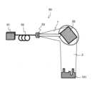
この光学回折素子(DOE)を用いたレーザ加工装置では、図5に示すように、1個の高出力レーザ源51から出射されるレーザ光を、光ファイバ52を介して、光学回折素子55に入射して、その反射(回折)光2を対象物101に照射して加工する。In this laser processing device using an optical diffraction element (DOE), as shown in Figure 5, laser light emitted from a single high-
しかしながら、高出力のレーザ光を光ファイバに伝送する場合、伝送距離が短いこととともに、光ファイバを屈曲させると屈曲箇所での漏れ光等の影響で発熱して光ファイバが破損するので、光ファイバの屈曲に制限あるという問題がある。However, when transmitting high-power laser light through optical fiber, there is a problem that the transmission distance is short, and there is a limit to how much the optical fiber can be bent, because bending the optical fiber can cause heat to be generated due to light leakage at the bent point, damaging the optical fiber.
また、高出力のレーザ光の入射により、光学回折素子(DOE)等の光学部品が発熱して位置ずれが生じ、焦点がずれるという問題もある。In addition, the incidence of high-power laser light can cause optical components such as a diffraction optical element (DOE) to heat up, resulting in misalignment and loss of focus.
上述したような課題を解決するために、本発明に係るレーザ加工装置は、所定のレーザ出力でレーザ光を出射する光源と、前記光源に接続する光ファイバと、前記光ファイバから出射される前記レーザ光が入射する光学回折素子とを備え、前記光源が、複数のレーザ源を備え、前記光ファイバが、前記複数のレーザ源それぞれに接続し、前記光学回折素子に、前記光ファイバから出射されるそれぞれの前記レーザ光が入射し、前記光学回折素子それぞれで反射する回折光が、略同一の強度分布、かつ、略同一の焦点位置で対象物に結像し、前記複数のレーザ源における1つのレーザ源から出射するレーザ光の伝送距離が、単一のレーザで構成され前記複数のレーザ源と同等のレーザ出力を出射する光源から出射するレーザ光の伝送可能距離に比べて長く、前記光ファイバの長さが50m以上300m以下であることを特徴とする。
In order to solve the above-mentioned problems, the laser processing apparatus according to the present invention comprises a light source that emits laser light at a predetermined laser output, an optical fiber connected to the light source, and an optical diffraction element into which the laser light emitted from the optical fiber is incident, the light source comprises a plurality of laser sources, the optical fiber is connected to each of the plurality of laser sources, the laser light emitted from the optical fiber is incident on the optical diffraction element, and the diffracted light reflected by each of the optical diffraction elements is imaged on an object with approximately the same intensity distribution and at approximately the same focal position, the transmission distance of the laser light emitted from one of the plurality of laser sources is longer than the transmission distance of the laser light emitted from a light source that is composed of a single laser and emits a laser output equivalent to that of theplurality of lasersources, and the length of the optical fiber is 50 m or more and 300 m or less.
本発明によれば、長距離で光ファイバ伝送される高出力レーザ光を用いたレーザ加工装置を提供できる。According to the present invention, a laser processing device can be provided that uses high-power laser light transmitted over long distances via optical fiber.
<第1の実施の形態>
本発明の第1の実施の形態について図1を参照して説明する。First Embodiment
A first embodiment of the present invention will be described with reference to FIG.
<レーザ加工装置の構成>
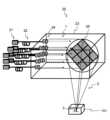
図1に、第1の実施の形態に係るレーザ加工装置10を示す。<Configuration of laser processing device>
FIG. 1 shows a
レーザ加工装置10は、レーザ源11と、光ファイバ12と、レーザヘッド13とを備える。The
レーザ源11は、9個のファイバレーザが並列に配置される。各レーザ源11の出力は1kWであり、レーザ光の波長は1064~1070nmである。1個のレーザ源11の大きさは、出射端側の端面が15cm×40cmで、長さが40cmであり、これらレーザ源は所定の位置に固定して利用される。The
光ファイバ12は、それぞれのレーザ源11の出力を伝搬する。光ファイバ12の長さは100mである。光ファイバ12の先端には、コリメートレンズ14が搭載される。コリメートレンズ14は、各光ファイバ12からの出力を平行なビームとして出射する。The
レーザヘッド13には、光ファイバ12の先端が接続され、光学回折素子(DOE)15を備える。レーザヘッド13の形状は、一辺が10cm~20cm程度の直方体である。The tip of the
光学回折素子(DOE)15は、反射型であり、レーザ源の個数に合わせて、9個の素子を備える。9個のレーザ源から光ファイバ12を介して出射されたレーザ光1を、9個の素子それぞれが反射して、対象物の表面において焦点を結ばせる。The diffractive optical element (DOE) 15 is a reflective type and has nine elements, matching the number of laser sources. The nine elements reflect the
各光学回折素子15は15mm×15mm程度であり、1枚の基板上に集積して形成される。光学回折素子15の表面には、微細な凹凸構造が形成されている。光学回折素子15(基板)の材料には、金、銀、銅、アルミニウム、または炭化ケイ素、ダイヤモンド、窒化アルミ、シリコン等を用いることができ、熱伝導の良い材料が望ましい。Each
ここで、光ファイバ12の先端から光学回折素子15の距離は10cm程度であり、光学回折素子15から対象物までの距離は光学回折素子の凹凸構造の設計によって任意に設計することができ、例えば、レーザ加工装置などにおいては数10cmから100cm程度に設計される。Here, the distance from the tip of the
光ファイバ12の先端から出射されるレーザ光1は、波面が進行方向に対して垂直な直線である平面波であり、その強度はガウス分布である。レーザ光1は光学回折素子15で反射され回折が生じ、回折光2が対象物101表面で結像して、対象物101を加工する。The
このとき、光学回折素子15それぞれの表面に形成された凹凸構造によって、結像位置における光のビーム3の断面の形状と光強度分布を成形することができる。以下、凹凸構造は、凹凸の形状および凹凸のレイアウト(配置)を含む。At this time, the unevenness structure formed on the surface of each
このように、光学回折素子15それぞれの表面に所定の凹凸構造を施すことにより、この凹凸構造で回折された、それぞれの光(回折光)2が対象物101表面で所定のパターンで結像する。その結果、複数の所定のパターンが重なって結像する。換言すれば、対象物101表面で所定のパターンに結像するように、光学回折素子15の表面の凹凸構造を設計できる。In this way, by providing a predetermined uneven structure on the surface of each
本実施の形態においては、光学回折素子15の表面の凹凸構造は、9個の光学回折素子15で回折する光2それぞれが、対象物101表面で結像するビーム3内で均一な強度分布を有し、略同一の強度分布、かつ、略同一の焦点位置で結像するにように設計される。ここで、対象物101表面で結像するビーム3の形状は0.2mm×0.2mm程度の矩形または0.2mm径程度の円形である。In this embodiment, the uneven structure on the surface of the
従来技術において、光学回折素子を用いずに、複数のレーザ源と、複数のレンズやミラー等の光学部品を用いる場合には、対象物101表面で結像するビーム内での強度分布が不均一になる。その結果、複数のビームを重ね合わせて加工する際に、各ビームの焦点を合わせて、所定の面積で光強度を高めることは困難である。In conventional technology, when multiple laser sources and multiple optical components such as lenses and mirrors are used without using an optical diffraction element, the intensity distribution in the beam focused on the surface of the
一方、本実施の形態によれば、各ビームが均一な強度分布を有するので、容易に各ビームの焦点を合わせて、所定の面積で光強度を高めて、レーザ加工を実施できる。On the other hand, according to the present embodiment, since each beam has a uniform intensity distribution, it is possible to easily focus each beam and increase the light intensity in a specified area to perform laser processing.
<レーザ加工装置の効果>
本実施の形態に係るレーザ加工装置10の効果について説明する。<Effects of laser processing equipment>
The effects of the
高出力レーザの光ファイバでの伝送可能距離は、レーザの出力と距離の積を基に推定される。例えば、レーザの出力と距離の積を300km・Wとする場合、単一のレーザ源を備え、出力が6.3kWのレーザ加工装置の光ファイバ伝送距離は、300km・W÷6.3kW=47.6mと推定される。 The transmission distance of a high-power laser through an optical fiber is estimated based on the product of the laser power and the distance. For example, if the product of the laser power and the distance is 300 km W, the optical fiber transmission distance of a laser processing device equipped with a single laser source and having an output of 6.3 kW is estimated to be 300km W ÷ 6.3kW = 47.6 m.
このように、従来の10kWクラスの従来のレーザ加工装置では、レーザ源からレーザヘッドまでの距離が高々数十メートルに限られる。Thus, in conventional 10 kW class laser processing devices, the distance from the laser source to the laser head is limited to a maximum of several tens of meters.
また、10kW程度の高出力レーザ光を光ファイバに伝搬させる場合、光ファイバを屈曲させると屈曲箇所での漏れ光等の影響で発熱して光ファイバが破損するので、光ファイバの曲げ半径を数十センチ以下にできないなどの制限もある。In addition, when transmitting high-power laser light of about 10 kW through an optical fiber, bending the optical fiber can cause heat to be generated due to light leakage at the bent point, causing the optical fiber to break, so there are restrictions such as not allowing the bending radius of the optical fiber to be less than a few tens of centimeters.
一方、本実施の形態に係るレーザ加工装置では、光源は9個のレーザ源からなるので、1個のレーザ源の出力を1kWとして、合計9kWのレーザ光が出射される。出射されるレーザ光は、DOE素子でのパターン変換損失(30%程度)を考慮して、対象物に6.3kWの出力で照射される。このときの1つのレーザに対する伝送距離は300km・W÷1kW=300mである。 On the other hand, in the laser processing device according to the present embodiment, the light source is composed of nine laser sources, and therefore, assuming that each laser source has an output of 1 kW, a total of 9 kW of laser light is emitted. The emitted laser light is irradiated to the object with an output of 6.3 kW, taking into account the pattern conversion loss (approximately 30%) in the DOE element. In this case, the transmission distance for one laser is 300km·W ÷ 1kW = 300 m.
以上より、従来のレーザ加工装置のファイバの伝送距離を考慮すると、本実施の形態に係るレーザ加工装置のファイバは50m以上の長さで効果を奏し、100m以上300m以下の長さが望ましい。From the above, considering the transmission distance of the fiber of conventional laser processing devices, the fiber of the laser processing device of this embodiment is effective at a length of 50 m or more, and a length of 100 m or more and 300 m or less is preferable.
さらに、光ファイバ内を伝搬するレーザ光の出力が1kW程度なので、光ファイバの屈曲箇所の発熱による破損を抑制できる。Furthermore, since the output of the laser light propagating through the optical fiber is approximately 1 kW, damage caused by heat generation at the bent points of the optical fiber can be suppressed.
このように、本実施の形態に係るレーザ加工装置によれば、光ファイバ伝送距離を延伸できるので、10kW出力のレーザ加工装置において、レーザ源からレーザヘッドまでの距離が延伸できる。その結果、数百メートルの光ファイバを利用でき、光ファイバの曲げ半径の自由度を高めて、光ファイバでの光損失による発熱にともなう光ファイバの破断などのリスクを抑制できる。In this way, the laser processing device according to the present embodiment can extend the optical fiber transmission distance, so that in a 10 kW output laser processing device, the distance from the laser source to the laser head can be extended. As a result, optical fibers of several hundred meters can be used, the degree of freedom of the bending radius of the optical fiber can be increased, and the risk of optical fiber breakage due to heat generation caused by optical loss in the optical fiber can be reduced.
また、本実施の形態に係るレーザ加工装置によれば、出力を複数個のレーザ源に分割することにより、例えば、9個のレーザ源の出射光が伝搬するそれぞれの経路において、光ファイバ、DOE素子などの1部の構成部品が故障しても、他の故障部品を含まない経路を動作させることができる。そこで、トータルでのレーザ出力の低下を最低限に抑えて、レーザ加工を実施できる。その結果、レーザ加工のスループットを維持して部品交換、メンテナンスを実施できる。In addition, according to the laser processing device of this embodiment, by dividing the output into multiple laser sources, even if some components such as optical fibers or DOE elements fail in each path along which the emitted light from, for example, nine laser sources propagates, it is possible to operate the path that does not include the other failed components. Therefore, laser processing can be performed while minimizing the decrease in total laser output. As a result, parts replacement and maintenance can be performed while maintaining the throughput of laser processing.
また、個々のレーザ出力を重ね合わせて所定のレーザ加工出力にできるため、レーザ出力を容易に調整でき、定期的にレーザ源などのメンテナンスを実施できるので、冗長性の高い利用が可能になる。In addition, since individual laser outputs can be superimposed to achieve a specified laser processing output, the laser output can be easily adjusted and maintenance of the laser source, etc. can be performed regularly, allowing for highly redundant use.
以上のように、本実施の形態に係るレーザ加工装置は、遠隔に配置する複数のレーザ源から光ファイバ、小型レーザヘッドを介して光学回折素子でレーザ光を回折させて加工できるので、密閉空間、例えば廃内や船舶のタンク内等にレーザ光を導入してレーザ加工作業を実施できる。As described above, the laser processing device of this embodiment can diffract laser light using an optical diffraction element from multiple laser sources located remotely via optical fiber and a small laser head, making it possible to introduce laser light into enclosed spaces, such as inside abandoned buildings or tanks on ships, to perform laser processing work.
また、本実施の形態に係るレーザ加工装置は、小型で軽量なので、ロボットアームに搭載して、密閉空間内で、遠隔操作でレーザ加工作業を実施できる。In addition, since the laser processing device of this embodiment is small and lightweight, it can be mounted on a robot arm and laser processing operations can be performed remotely within an enclosed space.
また、単一のレーザ源を用いる場合、高出力のレーザ光の入射により、光学回折素子(DOE)等の光学部品が発熱して位置ずれが生じ、焦点がずれる。本実施の形態に係るレーザ加工装置によれば、出力が複数個のレーザ源に分割されるので、光学回折素子(DOE)等の光学部品に高出力のレーザ光は入射されない。その結果、発熱による光学部品の位置ずれは抑制され、焦点がずれも抑制される。Furthermore, when a single laser source is used, the incidence of high-power laser light causes optical components such as a diffraction optical element (DOE) to heat up, resulting in misalignment and focus shifting. With the laser processing device according to this embodiment, the output is split between multiple laser sources, so high-power laser light is not incident on optical components such as a diffraction optical element (DOE). As a result, misalignment of optical components due to heat generation is suppressed, and focus shifting is also suppressed.
さらに、本実施の形態では、光学回折素子(DOE)の材料に熱伝導の良い材料を用いるので、発熱の影響をさらに抑制できる。Furthermore, in this embodiment, a material with good thermal conductivity is used for the optical diffraction element (DOE), which further reduces the effects of heat generation.
<第2の実施の形態>
本発明の第2の実施の形態に係るレーザ加工装置について図2を参照して説明する。本実施の形態に係るレーザ加工装置は、第1の実施の形態に係るレーザ加工装置と、略同様の構成を備え、略同様の効果を奏するが、対象物での回折光の焦点位置が異なる。Second Embodiment
A laser processing device according to a second embodiment of the present invention will be described with reference to Fig. 2. The laser processing device according to this embodiment has substantially the same configuration as the laser processing device according to the first embodiment and achieves substantially the same effects, but the focal position of the diffracted light on the target object is different.
<レーザ加工装置の構成>
図2に、第2の実施の形態に係るレーザ加工装置20を示す。<Configuration of laser processing device>
FIG. 2 shows a
レーザ加工装置20は、レーザ源21と、光ファイバ22と、レーザヘッド23とを備え、レーザヘッド23には、光ファイバ22の先端が接続され、光学回折素子(DOE)25を備える。The
ここで、光学回折素子25それぞれの表面に所定の凹凸構造を施すことにより、この凹凸構造で回折された、それぞれの光(回折光)2が対象物101表面で所定のパターンで結像する。その結果、複数の所定のパターンが重なって結像する。換言すれば、対象物101表面で所定のパターンに結像するように、光学回折素子25の表面の凹凸構造を設計できる。Here, by providing a predetermined uneven structure on the surface of each of the
本実施の形態では、それぞれの回折光2について対象物101表面で結像するビームの焦点3が対象物101の所定の深さにわたってそれぞれに位置するように、光学回折素子25の表面の凹凸構造が設計される。その結果、焦点は、対象物101の表面から10mm程度の深さにわたって等間隔に位置する。In this embodiment, the uneven structure of the surface of the
このように、本実施の形態においては、光学回折素子25の表面の凹凸構造は、9個の光学回折素子25で回折する光2それぞれが、対象物101の深さ方向にわたって所定の略同一の焦点位置で結像するように設計され、加工平面の奥行方向(対象物101の深さ方向)にもビームを制御できる。Thus, in this embodiment, the uneven structure on the surface of the
このように、本実施の形態によれば、各ビームの焦点が対象物の所定の深さにわたって位置するようにして、レーザ加工を実施できる。その結果、対象物の所定の深さにわたって効率的に加工できるので、層厚の厚い構造物等の加工(切断)を高速で実施することができる。In this way, according to the present embodiment, laser processing can be performed by positioning the focal points of each beam over a predetermined depth of the object. As a result, processing can be performed efficiently over a predetermined depth of the object, so that processing (cutting) of structures with thick layers can be performed at high speed.
以上のように、本実施の形態に係るレーザ加工装置は、遠隔に配置する複数のレーザ源から光ファイバ、小型レーザヘッドを介して光学回折素子でレーザ光を回折させて加工できるので、炉内や船舶のタンク内等の密閉空間にレーザ光を導入してレーザ加工作業を実施できる。As described above, the laser processing device of this embodiment can diffract laser light using an optical diffraction element from multiple laser sources located remotely via optical fiber and a small laser head, making it possible to introduce laser light into enclosed spaces such as inside a furnace or a ship's tank to perform laser processing operations.
<第3の実施の形態>
本発明の第3の実施の形態に係るレーザ加工装置について図3を参照して説明する。本実施の形態に係るレーザ加工装置は、第1の実施の形態に係るレーザ加工装置と、略同様の構成を備え、略同様の効果を奏するが、可動ステージを備える点で異なる。詳細を以下に説明する。Third Embodiment
A laser processing apparatus according to a third embodiment of the present invention will be described with reference to Fig. 3. The laser processing apparatus according to this embodiment has substantially the same configuration as the laser processing apparatus according to the first embodiment and achieves substantially the same effects, but differs in that it has a movable stage. Details will be described below.
<レーザ加工装置の構成>
図3に、第3の実施の形態に係るレーザ加工装置30を示す。<Configuration of laser processing device>
FIG. 3 shows a
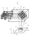
レーザ加工装置30は、レーザ源31と、光ファイバ32と、レーザヘッド33と、光学回折素子35と、対象物(被加工物)101を配置するステージ36を備える。The
ステージ36には、対象物101が配置され、ステージ36を水平方向(x方向、y方向)に外部から電気などで駆動することにより、ビーム3の対象物101での焦点位置を移動させ、対象物101を加工する。ここで、ステージを垂直方向(z方向)に駆動してもよい。The
光ファイバから出射されるレーザ光1は、波面が進行方向に対して垂直な直線である平面波であり、その強度はガウス分布である。レーザ光は光学回折素子35で反射され、回折光2となって、対象物101表面で結像して、対象物101を加工する。The
このように対象物に回折光が結像した状態で、ステージを駆動することにより、回折格子の焦点が対象物内を移動して、対象物を加工する。With the diffracted light focused on the object in this way, the stage is driven so that the focus of the diffraction grating moves within the object, thereby processing the object.
ここで、光学回折素子35それぞれの表面に所定の凹凸構造を施すことにより、この凹凸構造で回折された、それぞれの光(回折光)2が対象物101表面で所定のパターンで結像する。その結果、複数の所定のパターンが重なって結像する。換言すれば、対象物101表面で所定のパターンに結像するように、光学回折素子35の表面の凹凸構造を設計できる。対象物表面で結像するパターンとして、円形、矩形、リング状形状など多様なパターンを形成できる。Here, by providing a predetermined uneven structure on the surface of each of the
本実施の形態においては、対象物表面で結像するビームが所定の複数のパターンを形成するように光学回折素子の表面の凹凸構造を設計できる。In this embodiment, the uneven structure of the surface of the optical diffraction element can be designed so that the beam focused on the object surface forms multiple predetermined patterns.
このように、本実施の形態においては、光学回折素子15の表面の凹凸構造は、光学回折素子で回折する光それぞれが、対象物表面で所定の複数のパターン(形状)で結像するように設計される。Thus, in this embodiment, the uneven structure on the surface of the
従来技術において、光学回折素子を用いずに、複数のレーザ源に対して、複数のレンズやミラー等の光学部品を用いて、複数のビームを重ね合わせて加工する場合には、多数の光学部品とともに複雑な光学系の調整が必要になる。In conventional technology, when multiple beams are superimposed and processed using multiple optical components such as multiple lenses and mirrors for multiple laser sources without using optical diffraction elements, it is necessary to adjust a complex optical system along with numerous optical components.
一方、本実施の形態によれば、各ビームが所定の複数のパターンを有するので、所定の複数のパターンを組み合わせて、容易にサブミクロンから数ミクロンの高精度でのレーザ加工を実施できる。On the other hand, according to this embodiment, each beam has a predetermined number of patterns, so that by combining the predetermined number of patterns, laser processing can be easily performed with high precision of submicrons to several microns.
以上のように、本実施の形態に係るレーザ加工装置は、遠隔に配置する複数のレーザ源から光ファイバ、小型レーザヘッドを介して光学回折素子でレーザ光を回折させて高精度でのレーザ加工を実施できる。As described above, the laser processing apparatus of this embodiment can perform high-precision laser processing by diffracting laser light from multiple laser sources located remotely via optical fiber and a small laser head using an optical diffraction element.
本発明の実施の形態では、反射型の光学回折素子を用いたが、図4に示すように、透過型の光学回折素子を用いてもよい。In the embodiment of the present invention, a reflective optical diffraction element is used, but a transmissive optical diffraction element may also be used, as shown in Figure 4.
本発明の実施の形態では、9個のレーザ源を用いたが、数に限りはなく、複数であればよい。また、9個のレーザ源が並列に配置される例を示したが、配置はこれに限らず、光ファイバを介して光学回折素子にレーザ光を入射できるよう配置されればよい。In the embodiment of the present invention, nine laser sources are used, but there is no limit to the number, as long as there is more than one. Also, while an example has been shown in which nine laser sources are arranged in parallel, the arrangement is not limited to this, and it is sufficient that the laser sources are arranged so that laser light can be incident on the optical diffraction element via an optical fiber.
ここで、本発明の実施の形態で用いるレーザ源は、従来の高出力レーザの出力10kWを複数個(少なくとも2個)に分割するので、最大で5kWの出力を有する。また、金属、樹脂などの対象物の加工を考慮すると、0.5kWの出力を要する。したがって、本発明の実施の形態で用いるレーザ源の出力は、0.5kW以上5kW以下が望ましい。Here, the laser source used in the embodiment of the present invention has a maximum output of 5 kW, since the 10 kW output of a conventional high-power laser is divided into multiple parts (at least two parts). Also, when considering processing of objects such as metals and resins, an output of 0.5 kW is required. Therefore, the output of the laser source used in the embodiment of the present invention is preferably 0.5 kW or more and 5 kW or less.
本発明の実施の形態では、レーザ源の個数に合わせて、9個の光学回折素子を備える例を示したが、これに限らず、複数の光学回折素子を備えてもよい。レーザ源の個数に合わせなくても、複数のレーザ光が1個の光学回折素子に入射されてもよいし、レーザ光を分割して複数の光学回折素子に入射させてもよい。In the embodiment of the present invention, an example is shown in which nine optical diffraction elements are provided to match the number of laser sources, but this is not limiting, and multiple optical diffraction elements may be provided. Even if not matching the number of laser sources, multiple laser beams may be incident on one optical diffraction element, or the laser beam may be split and incident on multiple optical diffraction elements.
本発明の実施の形態では、9個の光学回折素子を1枚の基板に集積させる例を示したが、これに限らず、1枚の基板に集積させずに各光学回折素子を配置してもよい。In the embodiment of the present invention, an example is shown in which nine optical diffraction elements are integrated on a single substrate, but this is not limited thereto, and each optical diffraction element may be arranged without being integrated on a single substrate.
本発明の実施の形態では、レーザ加工装置の構成、製造方法などにおいて、各構成部の構造、寸法、材料等の一例を示したが、これに限らない。レーザ加工装置の機能を発揮し効果を奏するものであればよい。In the embodiment of the present invention, examples of the structure, dimensions, materials, etc. of each component in the configuration and manufacturing method of the laser processing device are shown, but the present invention is not limited to these. Anything that can demonstrate the function and effect of the laser processing device will suffice.
本発明は、工業分野における金属、樹脂などの加工や建設分野での建造物の切断などに適用することができる。The present invention can be applied to the processing of metals, resins, etc. in the industrial field and the cutting of structures in the construction field.
10 レーザ加工装置
11 レーザ源
12 光ファイバ
13 レーザヘッド
14 コリメートレンズ
15 光学回折素子10
Claims (7)
Translated fromJapanese前記光源に接続する光ファイバと、
前記光ファイバから出射される前記レーザ光が入射する光学回折素子とを備え、
前記光源が、複数のレーザ源を備え、
前記光ファイバが、前記複数のレーザ源それぞれに接続し、
前記光学回折素子に、前記光ファイバから出射されるそれぞれの前記レーザ光が入射し、
前記光学回折素子それぞれで反射する回折光が、略同一の強度分布、かつ、略同一の焦点位置で対象物に結像し、
前記複数のレーザ源における1つのレーザ源から出射するレーザ光の伝送距離が、単一のレーザで構成され前記複数のレーザ源と同等のレーザ出力を出射する光源から出射するレーザ光の伝送可能距離に比べて長く、
前記光ファイバの長さが50m以上300m以下である、レーザ加工装置。 A light source that emits a laser beam with a predetermined laser output;
an optical fiber connected to the light source;
an optical diffraction element onto which the laser light emitted from the optical fiber is incident,
the light source comprises a plurality of laser sources;
the optical fiber is connected to each of the plurality of laser sources;
The laser light emitted from the optical fiber is incident on the optical diffraction element,
the diffracted light reflected by each of the optical diffraction elements forms an image on an object with substantially the same intensity distribution and substantially the same focal position;
a transmission distance of a laser beam emitted from one of the plurality of laser sources islonger than a transmission distance of a laser beam emitted from a light source that is composed of a single laser and emits a laser output equivalent to that of the plurality of laser sources;
A laser processing device,wherein the length of the optical fiber is 50 m or more and 300 m or less .
請求項1に記載のレーザ加工装置。 2. The laser processing apparatus accordingto claim 1 , wherein the output of the laser source is 0.5 kW or more and 5 kW or less.
請求項1又は請求項2に記載のレーザ加工装置。 3. The laser processing apparatusaccording to claim1 , wherein the uneven structure on the surface of the optical diffraction element is designed so that the intensity distribution in the beam when the diffracted light is imaged on the object is uniform.
請求項1から請求項3のいずれか一項に記載のレーザ加工装置。 4. The laser processing apparatus according to claim1 , wherein the uneven structure on the surface of the optical diffraction element is designed so that the focal point of the diffracted light is positioned over a predetermined depth of the object.
前記光学回折素子の表面の凹凸構造が、前記回折光が、前記対象物に所定のパターンで結像するように設計される
請求項1から請求項4のいずれか一項に記載のレーザ加工装置。 Equipped with a movable stage,
5. The laser processing apparatus according to claim1 , wherein the uneven structure on the surface of the optical diffraction element is designed so that the diffracted light is imaged in a predetermined pattern on the object.
請求項1から請求項5のいずれか一項に記載のレーザ加工装置。 The laser processing apparatus according to claim1 , wherein the optical diffraction element is of a reflective type.
Applications Claiming Priority (1)
| Application Number | Priority Date | Filing Date | Title |
|---|---|---|---|
| PCT/JP2020/025808WO2022003858A1 (en) | 2020-07-01 | 2020-07-01 | Laser processing device |
Publications (2)
| Publication Number | Publication Date |
|---|---|
| JPWO2022003858A1 JPWO2022003858A1 (en) | 2022-01-06 |
| JP7616220B2true JP7616220B2 (en) | 2025-01-17 |
Family
ID=79315818
Family Applications (1)
| Application Number | Title | Priority Date | Filing Date |
|---|---|---|---|
| JP2022532915AActiveJP7616220B2 (en) | 2020-07-01 | 2020-07-01 | Laser Processing Equipment |
Country Status (3)
| Country | Link |
|---|---|
| US (1) | US20230241712A1 (en) |
| JP (1) | JP7616220B2 (en) |
| WO (1) | WO2022003858A1 (en) |
Citations (6)
| Publication number | Priority date | Publication date | Assignee | Title |
|---|---|---|---|---|
| JP2015017498A (en) | 2008-08-20 | 2015-01-29 | フォロ エナジー インコーポレーティッドForo Energy Inc. | Laser excavation facility for advancement of borehole using laser |
| JP2017537334A (en) | 2014-08-27 | 2017-12-14 | ヌブル インク | Applications, methods and systems for material processing using visible Raman lasers |
| WO2018173101A1 (en) | 2017-03-21 | 2018-09-27 | 三菱電機株式会社 | Laser processing device |
| JP2019504770A (en) | 2016-01-29 | 2019-02-21 | クイェルベルク−シュティフトゥング | Apparatus and method for thermal machining |
| WO2019176953A1 (en) | 2018-03-12 | 2019-09-19 | 古河電気工業株式会社 | Optical fiber bundle provided with beam superposing mechanism |
| JP6608104B1 (en) | 2019-03-14 | 2019-11-20 | 三菱電機株式会社 | Laser apparatus and laser processing machine |
- 2020
- 2020-07-01JPJP2022532915Apatent/JP7616220B2/enactiveActive
- 2020-07-01USUS18/002,910patent/US20230241712A1/enactivePending
- 2020-07-01WOPCT/JP2020/025808patent/WO2022003858A1/ennot_activeCeased
Patent Citations (6)
| Publication number | Priority date | Publication date | Assignee | Title |
|---|---|---|---|---|
| JP2015017498A (en) | 2008-08-20 | 2015-01-29 | フォロ エナジー インコーポレーティッドForo Energy Inc. | Laser excavation facility for advancement of borehole using laser |
| JP2017537334A (en) | 2014-08-27 | 2017-12-14 | ヌブル インク | Applications, methods and systems for material processing using visible Raman lasers |
| JP2019504770A (en) | 2016-01-29 | 2019-02-21 | クイェルベルク−シュティフトゥング | Apparatus and method for thermal machining |
| WO2018173101A1 (en) | 2017-03-21 | 2018-09-27 | 三菱電機株式会社 | Laser processing device |
| WO2019176953A1 (en) | 2018-03-12 | 2019-09-19 | 古河電気工業株式会社 | Optical fiber bundle provided with beam superposing mechanism |
| JP6608104B1 (en) | 2019-03-14 | 2019-11-20 | 三菱電機株式会社 | Laser apparatus and laser processing machine |
Also Published As
| Publication number | Publication date |
|---|---|
| US20230241712A1 (en) | 2023-08-03 |
| JPWO2022003858A1 (en) | 2022-01-06 |
| WO2022003858A1 (en) | 2022-01-06 |
Similar Documents
| Publication | Publication Date | Title |
|---|---|---|
| JP7303538B2 (en) | Laser processing equipment | |
| US11471978B2 (en) | Laser oscillator, laser machining device in which same is used, and laser oscillation method | |
| TWI466748B (en) | Laser processing apparatus | |
| US8466074B2 (en) | Method for processing a substrate using a laser beam | |
| US20200408992A1 (en) | Optical fiber bundle with beam overlapping mechanism | |
| CN111438438A (en) | A kind of laser high-efficiency large-area dynamic interference processing device and method | |
| KR20130052947A (en) | Laser processing device using doe and micro lens array, and laser modification device for wafer dicing having the same | |
| CN115351445A (en) | Light beam combining device, light beam combining system, laser processing device and control method | |
| KR20180064599A (en) | Laser processing apparatus | |
| CN107442929B (en) | Fiber Array Line Generator | |
| JP7616220B2 (en) | Laser Processing Equipment | |
| JP2014013833A (en) | Laser beam reshaping device, laser beam reshaping method, laser processing device, and laser processing method | |
| US20240066630A1 (en) | Laser device for generating laser radiation and 3d printing device comprising such a laser device | |
| JP5106130B2 (en) | Laser beam irradiation method and laser beam irradiation apparatus | |
| JP6043773B2 (en) | Sheet metal processing method using direct diode laser light and direct diode laser processing apparatus for executing the same | |
| CN119836335A (en) | Laser system and method for laser machining a workpiece | |
| WO2023074182A1 (en) | Light-emitting device, laser processing system, light-emitting device manufacturing method, and laser processing system manufacturing method | |
| JP6035304B2 (en) | Direct diode laser processing apparatus and sheet metal processing method using the same | |
| JP2020060725A (en) | Laser oscillator and laser processing apparatus using the same | |
| CN110549012B (en) | Method and device for cryptographic cutting of multicolor ultrashort pulse optical fiber | |
| JP6949289B1 (en) | Laser device | |
| JP5420172B2 (en) | Laser equipment | |
| EP4467274A1 (en) | Laser irradiation method and laser irradiation device | |
| KR20250137692A (en) | High-power laser system for forming a laser irradiation zone with specific dimensions and power density distribution for thermal surface treatment applications. | |
| JP2023168639A (en) | Laser irradiation method |
Legal Events
| Date | Code | Title | Description |
|---|---|---|---|
| A621 | Written request for application examination | Free format text:JAPANESE INTERMEDIATE CODE: A621 Effective date:20221109 | |
| A131 | Notification of reasons for refusal | Free format text:JAPANESE INTERMEDIATE CODE: A131 Effective date:20231212 | |
| A521 | Request for written amendment filed | Free format text:JAPANESE INTERMEDIATE CODE: A523 Effective date:20240213 | |
| A131 | Notification of reasons for refusal | Free format text:JAPANESE INTERMEDIATE CODE: A131 Effective date:20240604 | |
| A521 | Request for written amendment filed | Free format text:JAPANESE INTERMEDIATE CODE: A523 Effective date:20240802 | |
| TRDD | Decision of grant or rejection written | ||
| A01 | Written decision to grant a patent or to grant a registration (utility model) | Free format text:JAPANESE INTERMEDIATE CODE: A01 Effective date:20241203 | |
| A61 | First payment of annual fees (during grant procedure) | Free format text:JAPANESE INTERMEDIATE CODE: A61 Effective date:20241216 | |
| R150 | Certificate of patent or registration of utility model | Ref document number:7616220 Country of ref document:JP Free format text:JAPANESE INTERMEDIATE CODE: R150 | |
| S533 | Written request for registration of change of name | Free format text:JAPANESE INTERMEDIATE CODE: R313533 |