JP7615256B2 - Semiconductor Device - Google Patents
Semiconductor DeviceDownload PDFInfo
- Publication number
- JP7615256B2 JP7615256B2JP2023152061AJP2023152061AJP7615256B2JP 7615256 B2JP7615256 B2JP 7615256B2JP 2023152061 AJP2023152061 AJP 2023152061AJP 2023152061 AJP2023152061 AJP 2023152061AJP 7615256 B2JP7615256 B2JP 7615256B2
- Authority
- JP
- Japan
- Prior art keywords
- film
- oxide semiconductor
- insulating film
- transistor
- oxygen
- Prior art date
- Legal status (The legal status is an assumption and is not a legal conclusion. Google has not performed a legal analysis and makes no representation as to the accuracy of the status listed.)
- Active
Links
Images


Classifications
- H—ELECTRICITY
- H10—SEMICONDUCTOR DEVICES; ELECTRIC SOLID-STATE DEVICES NOT OTHERWISE PROVIDED FOR
- H10D—INORGANIC ELECTRIC SEMICONDUCTOR DEVICES
- H10D30/00—Field-effect transistors [FET]
- H10D30/60—Insulated-gate field-effect transistors [IGFET]
- H10D30/67—Thin-film transistors [TFT]
- H10D30/674—Thin-film transistors [TFT] characterised by the active materials
- H10D30/6755—Oxide semiconductors, e.g. zinc oxide, copper aluminium oxide or cadmium stannate
- H—ELECTRICITY
- H10—SEMICONDUCTOR DEVICES; ELECTRIC SOLID-STATE DEVICES NOT OTHERWISE PROVIDED FOR
- H10D—INORGANIC ELECTRIC SEMICONDUCTOR DEVICES
- H10D30/00—Field-effect transistors [FET]
- H10D30/01—Manufacture or treatment
- H10D30/021—Manufacture or treatment of FETs having insulated gates [IGFET]
- H10D30/031—Manufacture or treatment of FETs having insulated gates [IGFET] of thin-film transistors [TFT]
- H—ELECTRICITY
- H10—SEMICONDUCTOR DEVICES; ELECTRIC SOLID-STATE DEVICES NOT OTHERWISE PROVIDED FOR
- H10D—INORGANIC ELECTRIC SEMICONDUCTOR DEVICES
- H10D30/00—Field-effect transistors [FET]
- H10D30/60—Insulated-gate field-effect transistors [IGFET]
- H—ELECTRICITY
- H10—SEMICONDUCTOR DEVICES; ELECTRIC SOLID-STATE DEVICES NOT OTHERWISE PROVIDED FOR
- H10D—INORGANIC ELECTRIC SEMICONDUCTOR DEVICES
- H10D30/00—Field-effect transistors [FET]
- H10D30/60—Insulated-gate field-effect transistors [IGFET]
- H10D30/67—Thin-film transistors [TFT]
- H10D30/6704—Thin-film transistors [TFT] having supplementary regions or layers in the thin films or in the insulated bulk substrates for controlling properties of the device
- H—ELECTRICITY
- H10—SEMICONDUCTOR DEVICES; ELECTRIC SOLID-STATE DEVICES NOT OTHERWISE PROVIDED FOR
- H10D—INORGANIC ELECTRIC SEMICONDUCTOR DEVICES
- H10D30/00—Field-effect transistors [FET]
- H10D30/60—Insulated-gate field-effect transistors [IGFET]
- H10D30/67—Thin-film transistors [TFT]
- H10D30/6757—Thin-film transistors [TFT] characterised by the structure of the channel, e.g. transverse or longitudinal shape or doping profile
- H—ELECTRICITY
- H10—SEMICONDUCTOR DEVICES; ELECTRIC SOLID-STATE DEVICES NOT OTHERWISE PROVIDED FOR
- H10D—INORGANIC ELECTRIC SEMICONDUCTOR DEVICES
- H10D62/00—Semiconductor bodies, or regions thereof, of devices having potential barriers
- H10D62/10—Shapes, relative sizes or dispositions of the regions of the semiconductor bodies; Shapes of the semiconductor bodies
- H10D62/124—Shapes, relative sizes or dispositions of the regions of semiconductor bodies or of junctions between the regions
- H—ELECTRICITY
- H10—SEMICONDUCTOR DEVICES; ELECTRIC SOLID-STATE DEVICES NOT OTHERWISE PROVIDED FOR
- H10D—INORGANIC ELECTRIC SEMICONDUCTOR DEVICES
- H10D30/00—Field-effect transistors [FET]
- H10D30/60—Insulated-gate field-effect transistors [IGFET]
- H10D30/67—Thin-film transistors [TFT]
- H10D30/6729—Thin-film transistors [TFT] characterised by the electrodes
- H10D30/673—Thin-film transistors [TFT] characterised by the electrodes characterised by the shapes, relative sizes or dispositions of the gate electrodes
- H10D30/6733—Multi-gate TFTs
- H10D30/6734—Multi-gate TFTs having gate electrodes arranged on both top and bottom sides of the channel, e.g. dual-gate TFTs
Landscapes
- Engineering & Computer Science (AREA)
- Physics & Mathematics (AREA)
- Condensed Matter Physics & Semiconductors (AREA)
- General Physics & Mathematics (AREA)
- Computer Hardware Design (AREA)
- Microelectronics & Electronic Packaging (AREA)
- Power Engineering (AREA)
- Thin Film Transistor (AREA)
- Manufacturing & Machinery (AREA)
- Chemical & Material Sciences (AREA)
- Plasma & Fusion (AREA)
- Chemical Kinetics & Catalysis (AREA)
- Materials Engineering (AREA)
- Composite Materials (AREA)
- Formation Of Insulating Films (AREA)
- Metal-Oxide And Bipolar Metal-Oxide Semiconductor Integrated Circuits (AREA)
- Semiconductor Memories (AREA)
- Internal Circuitry In Semiconductor Integrated Circuit Devices (AREA)
- Physical Deposition Of Substances That Are Components Of Semiconductor Devices (AREA)
- Physical Vapour Deposition (AREA)
- Chemical Vapour Deposition (AREA)
Description
Translated fromJapanese本発明は、絶縁膜及び電界効果トランジスタを有する半導体装置の作製方法に関する。The present invention relates to a method for manufacturing a semiconductor device having an insulating film and a field effect transistor.
液晶表示装置や発光表示装置に代表されるフラットパネルディスプレイの多くに用いられ
ているトランジスタは、ガラス基板上に形成されたアモルファスシリコン、単結晶シリコ
ンまたは多結晶シリコンなどのシリコン半導体によって構成されている。また、該シリコ
さン半導体を用いたトランジスタは、集積回路(IC)などにも利用されている。The transistors used in many flat panel displays, such as liquid crystal display devices and light-emitting display devices, are made of silicon semiconductors, such as amorphous silicon, single crystal silicon, or polycrystalline silicon, formed on a glass substrate. Transistors using such silicon semiconductors are also used in integrated circuits (ICs).
近年、シリコン半導体に代わって、半導体特性を示す金属酸化物をトランジスタに用いる
技術が注目されている。なお、本明細書中では、半導体特性を示す金属酸化物を酸化物半
導体とよぶことにする。In recent years, technology that uses metal oxides exhibiting semiconducting properties in transistors instead of silicon semiconductors has been attracting attention. In this specification, metal oxides exhibiting semiconducting properties are referred to as oxide semiconductors.
例えば、酸化物半導体として、酸化亜鉛、またはIn-Ga-Zn系酸化物を用いたトラ
ンジスタを作製し、該トランジスタを表示装置の画素のスイッチング素子などに用いる技
術が開示されている(特許文献1及び特許文献2参照)。For example, a technique has been disclosed in which a transistor is manufactured using zinc oxide or an In—Ga—Zn-based oxide as an oxide semiconductor and the transistor is used as a switching element of a pixel of a display device or the like (see
酸化物半導体を用いたトランジスタにおいて、酸化物半導体膜に含まれる酸素欠損は、ト
ランジスタの電気特性の不良に繋がる。例えば、膜中に酸素欠損が含まれている酸化物半
導体を用いたトランジスタは、しきい値電圧がマイナス方向に変動しやすく、ノーマリー
オン特性となりやすい。これは、酸化物半導体に含まれる酸素欠損に起因して電荷が生じ
てしまい、低抵抗化するためである。In a transistor using an oxide semiconductor, oxygen vacancies in the oxide semiconductor film lead to poor electrical characteristics of the transistor. For example, a transistor using an oxide semiconductor that has oxygen vacancies in the film is likely to have a negative shift in threshold voltage and to have normally-on characteristics. This is because charges are generated due to the oxygen vacancies in the oxide semiconductor, resulting in low resistance.
また、酸化物半導体膜に酸素欠陥が含まれると、経時変化や光ゲートBT(Bias-T
emperature)ストレス試験により、トランジスタの電気特性、代表的にはしき
い値電圧が変動してしまうという問題がある。In addition, if the oxide semiconductor film contains oxygen defects, deterioration over time and photo-gate BT (Bias-T
There is a problem in that the electrical characteristics of a transistor, typically the threshold voltage, fluctuates due to the stress test.
そこで、本発明の一態様は、酸化物半導体を用いた半導体装置において、酸素欠損の含有
量を低減することを課題の一とする。また、本発明の一態様は、酸化物半導体を用いた半
導体装置において、電気特性を向上させることを課題の一とする。In view of the above, an object of one embodiment of the present invention is to reduce the amount of oxygen vacancies in a semiconductor device including an oxide semiconductor, and to improve electrical characteristics of a semiconductor device including an oxide semiconductor.
本発明の一態様は、プラズマCVD法を用いて化学量論的組成を満たす酸素よりも多くの
酸素を含む酸化絶縁膜を形成することを特徴とする。One embodiment of the present invention is characterized in that an oxide insulating film containing more oxygen than the amount of oxygen in the stoichiometric composition is formed by a plasma CVD method.
また、本発明の一態様は、酸化物半導体膜を有するトランジスタと、当該トランジスタ上
に形成される保護膜とを有する半導体装置において、当該保護膜として、プラズマCVD
法を用いて化学量論的組成を満たす酸素よりも多くの酸素を含む酸化絶縁膜を形成するこ
とを特徴とする。Another embodiment of the present invention is a semiconductor device including a transistor having an oxide semiconductor film and a protective film formed over the transistor.
The present invention is characterized in that an oxide insulating film containing more oxygen than the oxygen that satisfies the stoichiometric composition is formed by using a method.
また、本発明の一態様は、酸化物半導体膜を有するトランジスタと、当該トランジスタ上
に形成される保護膜とを有する半導体装置において、真空排気された処理室内に載置され
た基板を180℃以上260℃以下に保持し、処理室に原料ガスを導入して処理室内にお
ける圧力を100Pa以上250Pa以下とし、処理室内に設けられる電極に0.17W
/cm2以上0.5W/cm2以下の高周波電力を供給する条件により、上記保護膜とし
て化学量論的組成を満たす酸素よりも多くの酸素を含む酸化絶縁膜を形成することを特徴
とする。Another embodiment of the present invention is a semiconductor device including a transistor including an oxide semiconductor film and a protective film formed over the transistor, in which a substrate placed in a treatment chamber that has been evacuated to a vacuum is maintained at a temperature greater than or equal to 180° C. and less than or equal to 260° C., a source gas is introduced into the treatment chamber to set the pressure in the treatment chamber to greater than or equal to 100 Pa and less than or equal to 250 Pa, and a 0.17 W electrode is provided in the treatment chamber.
The present invention is characterized in that an oxide insulating film containing more oxygen than the oxygen that satisfies the stoichiometric composition is formed as the protective film under conditions of supplying high-frequency power of 0.5 W/cm2 or more and 0.5 W/cm2 or less.
また、本発明の一態様は、酸化物半導体膜を有するトランジスタと、当該トランジスタ上
に形成される保護膜とを有する半導体装置において、真空排気された処理室内に載置され
た基板を180℃以上260℃以下に保持し、処理室に原料ガスを導入して処理室内にお
ける圧力を100Pa以上250Pa以下とし、処理室内に設けられる電極に0.17W
/cm2以上0.5W/cm2以下の高周波電力を供給する条件により、上記保護膜とし
て化学量論的組成を満たす酸素よりも多くの酸素を含む酸化絶縁膜を形成した後、加熱処
理を行い、保護膜に含まれる酸素を酸化物半導体膜に拡散させることを特徴とする。Another embodiment of the present invention is a semiconductor device including a transistor including an oxide semiconductor film and a protective film formed over the transistor, in which a substrate placed in a treatment chamber that has been evacuated to a vacuum is maintained at a temperature greater than or equal to 180° C. and less than or equal to 260° C., a source gas is introduced into the treatment chamber to set the pressure in the treatment chamber to greater than or equal to 100 Pa and less than or equal to 250 Pa, and a 0.17 W electrode is provided in the treatment chamber.
The present invention is characterized in that an oxide insulating film containing more oxygen than the oxygen satisfying the stoichiometric composition is formed as the protective film under conditions of supplying high-frequency power of 100 W/cm2 or more and 0.5 W/cm2 orless , and then heat treatment is performed to diffuse the oxygen contained in the protective film into the oxide semiconductor film.
また、本発明の一態様は、ゲート電極と、ゲート電極の一部とゲート絶縁膜を介して重な
る酸化物半導体膜と、酸化物半導体膜に接する一対の電極とを有するトランジスタと、酸
化物半導体膜上に設けられる保護膜と、を有し、保護膜は、電子スピン共鳴測定によるg
=2.001に現れる信号のスピン密度が1.5×10¹⁸spins/cm3未満であ
る酸化絶縁膜である。Another embodiment of the present invention includes a transistor including a gate electrode, an oxide semiconductor film overlapping with part of the gate electrode with a gate insulating film therebetween, and a pair of electrodes in contact with the oxide semiconductor film; and a protective film provided over the oxide semiconductor film,
The spin density of the signal appearing at θ = 2.001 is less than 1.5 × 10¹⁸ spins/cm3 .
なお、一対の電極は、ゲート絶縁膜及び酸化物半導体膜の間に設けられる。または、一対
の電極は、酸化物半導体膜及び保護膜の間に設けられる。Note that the pair of electrodes is provided between the gate insulating film and the oxide semiconductor film, or between the oxide semiconductor film and the protective film.
また、本発明の一態様は、酸化物半導体膜と、酸化物半導体膜に接する一対の電極と、酸
化物半導体膜上に設けられるゲート絶縁膜と、酸化物半導体膜の一部とゲート絶縁膜を介
して重なるゲート電極とを有するトランジスタと、ゲート絶縁膜及びゲート電極を覆う保
護膜と、を有し、保護膜は、電子スピン共鳴測定によるg=2.001に現れる信号のス
ピン密度が1.5×10¹⁸spins/cm3未満である酸化絶縁膜であることを特徴
とする半導体装置である。Another embodiment of the present invention is a semiconductor device including a transistor including an oxide semiconductor film, a pair of electrodes in contact with the oxide semiconductor film, a gate insulating film provided over the oxide semiconductor film, and a gate electrode overlapping with part of the oxide semiconductor film with the gate insulating film interposed therebetween; and a protective film covering the gate insulating film and the gate electrode, wherein the protective film is an oxide insulating film in which a spin density of a signal appearing at g = 2.001 in electron spin resonance measurement is less than 1.5 × 10spins /cm3 .
酸化物半導体を有するトランジスタにおいて、トランジスタ上に形成される保護膜として
化学量論的組成を満たす酸素よりも多くの酸素を含む酸化絶縁膜を形成することで、更に
は当該保護膜から酸化物半導体膜に酸素を拡散させることで、酸化物半導体膜に含まれる
酸素欠損量を低減することができる。このため、本発明の一態様により、優れた電気特性
を有する半導体装置を作製することができる。In a transistor including an oxide semiconductor, by forming an oxide insulating film containing more oxygen than the oxygen in the stoichiometric composition as a protective film formed over the transistor, and by diffusing oxygen from the protective film into the oxide semiconductor film, the amount of oxygen vacancies in the oxide semiconductor film can be reduced. Thus, according to one embodiment of the present invention, a semiconductor device with excellent electrical characteristics can be manufactured.
以下では、本発明の実施の形態について図面を用いて詳細に説明する。ただし、本発明は
以下の説明に限定されず、本発明の趣旨及びその範囲から逸脱することなくその形態及び
詳細を様々に変更し得ることは、当業者であれば容易に理解される。従って、本発明は、
以下に示す実施の形態の記載内容に限定して解釈されるものではない。また、以下に説明
する実施の形態及び実施例において、同一部分または同様の機能を有する部分には、同一
の符号または同一のハッチパターンを異なる図面間で共通して用い、その繰り返しの説明
は省略する。Hereinafter, the embodiment of the present invention will be described in detail with reference to the drawings. However, the present invention is not limited to the following description, and it will be easily understood by those skilled in the art that the form and details of the present invention can be modified in various ways without departing from the spirit and scope of the present invention. Therefore, the present invention is
The present invention should not be construed as being limited to the description of the embodiments shown below. In the embodiments and examples described below, the same parts or parts having similar functions are denoted by the same reference numerals or the same hatch patterns in different drawings, and repeated description thereof will be omitted.
なお、本明細書で説明する各図において、各構成の大きさ、膜の厚さ、または領域は、明
瞭化のために誇張されている場合がある。よって、必ずしもそのスケールに限定されない
。In addition, in each figure described in this specification, the size of each component, the thickness of a film, or an area may be exaggerated for clarity, and therefore, the drawings are not necessarily limited to the scale.
また、本明細書にて用いる第1、第2、第3などの用語は、構成要素の混同を避けるため
に付したものであり、数的に限定するものではない。そのため、例えば、「第1の」を「
第2の」または「第3の」などと適宜置き換えて説明することができる。In addition, the terms "first,""second,""third," and the like used in this specification are used to avoid confusion of components, and are not intended to limit the number of components.
The terms "second" and "third" can be used interchangeably to explain the present invention.
「ソース」や「ドレイン」の機能は、回路動作において電流の方向が変化する場合などに
は入れ替わることがある。このため、本明細書においては、「ソース」や「ドレイン」の
用語は、入れ替えて用いることができるものとする。The functions of "source" and "drain" may be interchangeable when the direction of current flow changes during circuit operation. For this reason, in this specification, the terms "source" and "drain" can be used interchangeably.
本明細書において、フォトリソグラフィ工程を行った後にエッチング工程を行う場合は、
フォトリソグラフィ工程で形成したマスクはエッチング工程後に除去するものとする。In this specification, when an etching step is performed after a photolithography step,
The mask formed in the photolithography process is removed after the etching process.
(実施の形態1)
本実施の形態では、本発明の一態様である半導体装置、及び当該半導体装置の作製方法に
ついて図面を参照して説明する。(Embodiment 1)
In this embodiment, a semiconductor device which is one embodiment of the present invention and a method for manufacturing the semiconductor device will be described with reference to the drawings.
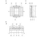
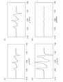
図1(A)乃至図1(C)に、半導体装置が有するトランジスタ10の上面図及び断面図
を示す。図1(A)はトランジスタ10の上面図であり、図1(B)は、図1(A)の一
点鎖線A-B間の断面図であり、図1(C)は、図1(A)の一点鎖線C-D間の断面図
である。なお、図1(A)では、明瞭化のため、トランジスタ10の構成要素の一部(例
えば、基板11、下地絶縁膜13、ゲート絶縁膜17)、保護膜23などを省略している
。1A to 1C show a top view and a cross-sectional view of a
図1(B)及び図1(C)に示すトランジスタ10は、下地絶縁膜13上に形成されるゲ
ート電極15と、下地絶縁膜13及びゲート電極15上に形成されるゲート絶縁膜17と
、ゲート絶縁膜17を介して、ゲート電極15と重なる酸化物半導体膜19と、酸化物半
導体膜19に接する一対の電極21と、を有する。また、ゲート絶縁膜17、酸化物半導
体膜19、及び一対の電極21を覆う保護膜23を有する。1B and 1C includes a
本実施の形態に示すトランジスタ10は、保護膜23が、化学量論的組成を満たす酸素よ
りも多くの酸素を含む酸化絶縁膜である。さらに好ましくは、保護膜23は、酸化物半導
体膜19に含まれる酸素欠損量以上の酸素を含む。化学量論的組成を満たす酸素よりも多
くの酸素を含む酸化絶縁膜は、加熱により酸素の一部が脱離する酸化絶縁膜である。この
ため、加熱により酸素の一部が脱離する酸化絶縁膜を保護膜23として設けることで、加
熱処理により酸化物半導体膜19に酸素を拡散させ、酸化物半導体膜19に含まれる酸素
欠損を補填することが可能である。この結果、酸化物半導体膜19に含まれる酸素欠損量
が低減され、しきい値電圧のマイナスシフトを抑制したトランジスタとなる。また、経時
変化や光ゲートBTストレスによって、しきい値電圧の変動が少なく、優れた電気特性を
有するトランジスタとなる。In the
なお、トランジスタ10においては、保護膜23に含まれる酸素は、直接、酸化物半導体
膜19に移動すると共に、ゲート絶縁膜17及び保護膜23が接する領域からゲート絶縁
膜17を介して、酸化物半導体膜19に移動する。Note that in the
また、保護膜23において、電子スピン共鳴測定によるg=2.001に現れる信号のス
ピン密度が1.5×10¹⁸spins/cm3未満、さらには1.0×1018spi
ns/cm3以下であることが好ましい。保護膜23のスピン密度が上記範囲を満たすこ
とで、酸化物半導体膜19及び保護膜23の界面、並びに保護膜23における欠陥を低減
することが可能であり、当該領域における電子のトラップを低減することができる。この
結果、トランジスタの電気特性において、異なるドレイン電圧におけるオン電流の立ち上
がり電圧が略同一となる。即ち、優れた電気特性を有するトランジスタを作製することが
できる。なお、保護膜23の上記スピン密度は加熱処理後の値である。In addition, in the
ns/cm3 or less. When the spin density of the
保護膜23としては、厚さが30nm以上500nm以下、好ましくは100nm以上4
00nm以下の酸化シリコン膜、酸化窒化シリコン膜等を用いることができる。The
A silicon oxide film, a silicon oxynitride film, or the like having a thickness of 00 nm or less can be used.
以下に、トランジスタ10の他の構成の詳細について説明する。The following describes in detail other configurations of
基板11の材質などに大きな制限はないが、少なくとも、後の熱処理に耐えうる程度の耐
熱性を有している必要がある。例えば、ガラス基板、セラミック基板、石英基板、サファ
イア基板等を、基板11として用いてもよい。また、シリコンや炭化シリコンなどの単結
晶半導体基板、多結晶半導体基板、シリコンゲルマニウム等の化合物半導体基板、SOI
基板等を適用することも可能であり、これらの基板上に半導体素子が設けられたものを、
基板11として用いてもよい。There are no significant limitations on the material of the
It is also possible to apply a substrate or the like, and a semiconductor element is provided on the substrate.
It may be used as the
また、基板11として、可撓性基板を用い、可撓性基板上に直接、下地絶縁膜13及びト
ランジスタ10を形成してもよい。または、基板11と下地絶縁膜13の間に剥離層を設
けてもよい。剥離層は、その上に半導体装置を一部あるいは全部完成させた後、基板11
より分離し、他の基板に転載するのに用いることができる。その際、トランジスタ10は
耐熱性の劣る基板や可撓性の基板にも転載できる。Alternatively, a flexible substrate may be used as the
In this case, the
下地絶縁膜13としては、酸化シリコン、酸化窒化シリコン、窒化シリコン、窒化酸化シ
リコン、酸化ガリウム、酸化ハフニウム、酸化イットリウム、酸化アルミニウム、酸化窒
化アルミニウム等がある。なお、下地絶縁膜13として、窒化シリコン、酸化ガリウム、
酸化ハフニウム、酸化イットリウム、酸化アルミニウム等を用いることで、基板11から
酸化物半導体膜19へ、アルカリ金属、水、水素等の不純物が拡散することを抑制できる
。The
By using hafnium oxide, yttrium oxide, aluminum oxide, or the like, diffusion of impurities such as alkali metals, water, and hydrogen from the
ゲート電極15は、アルミニウム、クロム、銅、タンタル、チタン、モリブデン、タング
ステンから選ばれた金属元素、または上述した金属元素を成分とする合金か、上述した金
属元素を組み合わせた合金等を用いて形成することができる。また、マンガン、ジルコニ
ウムのいずれか一または複数から選択された金属元素を用いてもよい。また、ゲート電極
15は、単層構造でも、二層以上の積層構造としてもよい。例えば、シリコンを含むアル
ミニウム膜の単層構造、アルミニウム膜上にチタン膜を積層する二層構造、窒化チタン膜
上にチタン膜を積層する二層構造、窒化チタン膜上にタングステン膜を積層する二層構造
、窒化タンタル膜または窒化タングステン膜上にタングステン膜を積層する二層構造、チ
タン膜と、そのチタン膜上にアルミニウム膜を積層し、さらにその上にチタン膜を形成す
る三層構造等がある。また、アルミニウムに、チタン、タンタル、タングステン、モリブ
デン、クロム、ネオジム、スカンジウムから選ばれた元素の膜、または複数組み合わせた
合金膜、もしくは窒化膜を用いてもよい。The
また、ゲート電極15は、インジウム錫酸化物、酸化タングステンを含むインジウム酸化
物、酸化タングステンを含むインジウム亜鉛酸化物、酸化チタンを含むインジウム酸化物
、酸化チタンを含むインジウム錫酸化物、インジウム亜鉛酸化物、酸化シリコンを添加し
たインジウム錫酸化物等の透光性を有する導電性材料を適用することもできる。また、上
記透光性を有する導電性材料と、上記金属元素の積層構造とすることもできる。The
また、ゲート電極15とゲート絶縁膜17との間に、In-Ga-Zn系酸窒化物半導体
膜、In-Sn系酸窒化物半導体膜、In-Ga系酸窒化物半導体膜、In-Zn系酸窒
化物半導体膜、Sn系酸窒化物半導体膜、In系酸窒化物半導体膜、金属窒化膜(InN
、ZnN等)等を設けることが好ましい。これらの膜は5eV以上、好ましくは5.5e
V以上の仕事関数を有し、酸化物半導体の電子親和力よりも大きい値であるため、酸化物
半導体を用いたトランジスタのしきい値電圧をプラスにすることができ、所謂ノーマリー
オフ特性のスイッチング素子を実現できる。例えば、In-Ga-Zn系酸窒化物半導体
膜を用いる場合、少なくとも酸化物半導体膜19より高い窒素濃度、具体的には7原子%
以上のIn-Ga-Zn系酸窒化物半導体膜を用いる。Between the
It is preferable to provide a film having a valence of 5 eV or more, preferably 5.5 eV or more.
Since the oxide semiconductor film has a work function of 10 V or more and a value larger than the electron affinity of the oxide semiconductor, the threshold voltage of a transistor using the oxide semiconductor can be made positive, and a switching element with so-called normally-off characteristics can be realized. For example, when an In—Ga—Zn-based oxynitride semiconductor film is used, the nitrogen concentration is at least higher than that of the
The above-mentioned In--Ga--Zn-based oxynitride semiconductor film is used.
ゲート絶縁膜17としては、例えば酸化シリコン、酸化窒化シリコン、窒化酸化シリコン
、窒化シリコン、酸化アルミニウム、酸化ハフニウム、酸化ガリウムまたはGa-Zn系
金属酸化物、などを用いればよく、積層または単層で設ける。また、ゲート絶縁膜17に
おいて酸化物半導体膜19に接する側に、加熱により酸素が脱離する酸化絶縁膜を用いて
もよい。ゲート絶縁膜17に加熱により酸素が脱離する膜を用いることで、酸化物半導体
膜19及びゲート絶縁膜17の界面における界面準位を低減することが可能であり、電気
特性の劣化の少ないトランジスタを得ることができる。また、ゲート絶縁膜17のゲート
電極側に、酸素、水素、水等のブロッキング効果を有する絶縁膜を設けることで、酸化物
半導体膜19からの酸素の外部への拡散と、外部から酸化物半導体膜19への水素、水の
侵入を防ぐことができる。酸素、水素、水等のブロッキング効果を有する絶縁膜としては
、酸化アルミニウム、酸化窒化アルミニウム、酸化ガリウム、酸化窒化ガリウム、酸化イ
ットリウム、酸化窒化イットリウム、酸化ハフニウム、酸化窒化ハフニウム等がある。The
また、ゲート絶縁膜17として、ハフニウムシリケート(HfSiOx)、窒素が添加さ
れたハフニウムシリケート(HfSixOyNz)、窒素が添加されたハフニウムアルミ
ネート(HfAlxOyNz)、酸化ハフニウム、酸化イットリウムなどのhigh-k
材料を用いることでトランジスタのゲートリークを低減できる。The
The use of this material can reduce gate leakage in transistors.
ゲート絶縁膜17の厚さは、5nm以上400nm以下、より好ましくは10nm以上3
00nm以下、より好ましくは50nm以上250nm以下とするとよい。The thickness of the
00 nm or less, and more preferably 50 nm or more and 250 nm or less.
酸化物半導体膜19は、少なくともインジウム(In)若しくは亜鉛(Zn)を含むこと
が好ましい。または、InとZnの双方を含むことが好ましい。また、該酸化物半導体を
用いたトランジスタの電気特性のばらつきを減らすため、それらと共に、スタビライザー
の一または複数を有することが好ましい。The
スタビライザーとしては、ガリウム(Ga)、スズ(Sn)、ハフニウム(Hf)、アル
ミニウム(Al)、またはジルコニウム(Zr)等がある。また、他のスタビライザーと
しては、ランタノイドである、ランタン(La)、セリウム(Ce)、プラセオジム(P
r)、ネオジム(Nd)、サマリウム(Sm)、ユウロピウム(Eu)、ガドリニウム(
Gd)、テルビウム(Tb)、ジスプロシウム(Dy)、ホルミウム(Ho)、エルビウ
ム(Er)、ツリウム(Tm)、イッテルビウム(Yb)、ルテチウム(Lu)等がある
。The stabilizer may be gallium (Ga), tin (Sn), hafnium (Hf), aluminum (Al), or zirconium (Zr). Other stabilizers include lanthanides such as lanthanum (La), cerium (Ce), and praseodymium (P).
r), neodymium (Nd), samarium (Sm), europium (Eu), gadolinium (
Examples of such elements include arsenic (Au), terbium (Tb), dysprosium (Dy), holmium (Ho), erbium (Er), thulium (Tm), ytterbium (Yb), and lutetium (Lu).
例えば、酸化物半導体として、酸化インジウム、酸化スズ、酸化亜鉛、二元系金属酸化物
であるIn-Zn系金属酸化物、Sn-Zn系金属酸化物、Al-Zn系金属酸化物、Z
n-Mg系金属酸化物、Sn-Mg系金属酸化物、In-Mg系金属酸化物、In-Ga
系金属酸化物、三元系金属酸化物であるIn-Ga-Zn系金属酸化物(IGZOとも表
記する)、In-Al-Zn系金属酸化物、In-Sn-Zn系金属酸化物、Sn-Ga
-Zn系金属酸化物、Al-Ga-Zn系金属酸化物、Sn-Al-Zn系金属酸化物、
In-Hf-Zn系金属酸化物、In-La-Zn系金属酸化物、In-Ce-Zn系金
属酸化物、In-Pr-Zn系金属酸化物、In-Nd-Zn系金属酸化物、In-Sm
-Zn系金属酸化物、In-Eu-Zn系金属酸化物、In-Gd-Zn系金属酸化物、
In-Tb-Zn系金属酸化物、In-Dy-Zn系金属酸化物、In-Ho-Zn系金
属酸化物、In-Er-Zn系金属酸化物、In-Tm-Zn系金属酸化物、In-Yb
-Zn系金属酸化物、In-Lu-Zn系金属酸化物、四元系金属酸化物であるIn-S
n-Ga-Zn系金属酸化物、In-Hf-Ga-Zn系金属酸化物、In-Al-Ga
-Zn系金属酸化物、In-Sn-Al-Zn系金属酸化物、In-Sn-Hf-Zn系
金属酸化物、In-Hf-Al-Zn系金属酸化物を用いることができる。Examples of oxide semiconductors include indium oxide, tin oxide, zinc oxide, binary metal oxides such as In-Zn-based metal oxides, Sn-Zn-based metal oxides, Al-Zn-based metal oxides, and Z
n-Mg metal oxide, Sn-Mg metal oxide, In-Mg metal oxide, In-Ga
system metal oxides, ternary metal oxides such as In-Ga-Zn system metal oxides (also written as IGZO), In-Al-Zn system metal oxides, In-Sn-Zn system metal oxides, Sn-Ga
-Zn-based metal oxides, Al-Ga-Zn-based metal oxides, Sn-Al-Zn-based metal oxides,
In-Hf-Zn based metal oxides, In-La-Zn based metal oxides, In-Ce-Zn based metal oxides, In-Pr-Zn based metal oxides, In-Nd-Zn based metal oxides, In-Sm
-Zn-based metal oxides, In-Eu-Zn-based metal oxides, In-Gd-Zn-based metal oxides,
In-Tb-Zn based metal oxides, In-Dy-Zn based metal oxides, In-Ho-Zn based metal oxides, In-Er-Zn based metal oxides, In-Tm-Zn based metal oxides, In-Yb
-Zn-based metal oxides, In-Lu-Zn-based metal oxides, and quaternary metal oxides such as In-S
n-Ga-Zn metal oxide, In-Hf-Ga-Zn metal oxide, In-Al-Ga
In-Zn based metal oxides, In-Sn-Al-Zn based metal oxides, In-Sn-Hf-Zn based metal oxides, and In-Hf-Al-Zn based metal oxides can be used.
なお、ここで、例えば、In-Ga-Zn系金属酸化物とは、InとGaとZnを主成分
として有する酸化物という意味であり、InとGaとZnの比率は問わない。また、In
とGaとZn以外の金属元素が入っていてもよい。In addition, for example, an In-Ga-Zn-based metal oxide means an oxide having In, Ga, and Zn as main components, and the ratio of In, Ga, and Zn does not matter.
Metal elements other than Ga and Zn may be included.
また、酸化物半導体として、InMO3(ZnO)m(m>0、且つ、mは整数でない)
で表記される材料を用いてもよい。なお、Mは、Ga、Fe、Mn及びCoから選ばれた
一の金属元素または複数の金属元素を示す。また、酸化物半導体として、In2SnO5
(ZnO)n(n>0、且つ、nは整数)で表記される材料を用いてもよい。In addition, the oxide semiconductor may be InMO3 (ZnO)m (m>0, and m is not an integer).
In addition, M represents one or more metal elements selected from Ga, Fe, Mn, and Co. In addition, as the oxide semiconductor, a material represented by the formula: In2 SnO5
A material expressed as (ZnO)n (n>0, and n is an integer) may be used.
例えば、In:Ga:Zn=1:1:1(=1/3:1/3:1/3)、In:Ga:Z
n=2:2:1(=2/5:2/5:1/5)、あるいはIn:Ga:Zn=3:1:2
(=1/2:1/6:1/3)の原子数比のIn-Ga-Zn系金属酸化物やその組成の
近傍の酸化物を用いることができる。あるいは、In:Sn:Zn=1:1:1(=1/
3:1/3:1/3)、In:Sn:Zn=2:1:3(=1/3:1/6:1/2)あ
るいはIn:Sn:Zn=2:1:5(=1/4:1/8:5/8)の原子数比のIn-
Sn-Zn系金属酸化物やその組成の近傍の酸化物を用いるとよい。なお、金属酸化物の
原子数比は、誤差として上記の原子数比のプラスマイナス20%の変動を含む。For example, In:Ga:Zn=1:1:1 (=1/3:1/3:1/3), In:Ga:Z
n=2:2:1 (=2/5:2/5:1/5), or In:Ga:Zn=3:1:2
In-Ga-Zn based metal oxides having an atomic ratio of In:Sn:Zn=1:1:1 (=1/2:1/6:1/3) or oxides having a similar composition can be used.
In- with an atomic ratio of In:Sn:Zn=2:1:3 (=1/3:1/6:1/2) or In:Sn:Zn=2:1:5 (=1/4:1/8:5/8)
It is preferable to use a Sn-Zn based metal oxide or an oxide having a composition close to that. Note that the atomic ratio of the metal oxide includes a variation of ±20% of the above atomic ratio as an error.
しかし、これらに限られず、必要とする半導体特性及び電気特性(電界効果移動度、しき
い値電圧等)に応じて適切な組成のものを用いればよい。また、必要とする半導体特性及
び電気特性を得るために、キャリア密度や不純物濃度、欠陥密度、金属元素と酸素の原子
数比、原子間距離、密度等を適切なものとすることが好ましい。However, the present invention is not limited to these, and an appropriate composition may be used depending on the required semiconductor characteristics and electrical characteristics (field effect mobility, threshold voltage, etc.). In order to obtain the required semiconductor characteristics and electrical characteristics, it is preferable to appropriately select the carrier density, impurity concentration, defect density, atomic ratio of metal element to oxygen, interatomic distance, density, etc.
例えば、In-Sn-Zn系金属酸化物では比較的容易に高い移動度が得られる。しかし
ながら、In-Ga-Zn系金属酸化物でも、バルク内欠陥密度を低くすることにより移
動度を上げることができる。For example, high mobility can be obtained relatively easily in In--Sn--Zn based metal oxides, but mobility can also be increased in In--Ga--Zn based metal oxides by lowering the bulk defect density.
また、酸化物半導体膜19に形成することが可能な金属酸化物は、エネルギーギャップが
2eV以上、好ましくは2.5eV以上、より好ましくは3eV以上である。このように
、エネルギーギャップの広い酸化物半導体を用いることで、トランジスタのオフ電流を低
減することができる。The energy gap of a metal oxide that can be formed for the
また、酸化物半導体膜19は、非晶質構造、単結晶構造、または多結晶構造であってもよ
い。The
また、酸化物半導体膜19は、例えば非単結晶を有してもよい。非単結晶は、例えば、C
AAC(C Axis Aligned Crystal)、多結晶、微結晶、非晶質部
の一以上を有する。非晶質部は、微結晶、CAACよりも欠陥準位密度が高い。また、微
結晶は、CAACよりも欠陥準位密度が高い。なお、CAACを有する酸化物半導体を、
CAAC-OS(C Axis Aligned Crystal Oxide Sem
iconductor)と呼ぶ。CAAC-OSは、例えば、c軸配向し、a軸または/
およびb軸はマクロに揃っていない。The
The oxide semiconductor has one or more of AAC (C-Axis Aligned Crystal), polycrystalline, microcrystalline, and amorphous parts. The amorphous parts have a higher density of defect states than the microcrystalline and CAAC. The microcrystalline parts have a higher density of defect states than the CAAC. Note that the oxide semiconductor having CAAC is
CAAC-OS (C Axis Aligned Crystal Oxide Sem
For example, the CAAC-OS has a c-axis orientation and an a-axis or/and
and the b axis is not macroscopically aligned.
酸化物半導体膜19は、例えば微結晶を有してもよい。なお、微結晶を有する酸化物半導
体を、微結晶酸化物半導体と呼ぶ。微結晶酸化物半導体膜は、例えば、1nm以上10n
m未満のサイズの微結晶(ナノ結晶ともいう。)を膜中に含む。The
The film contains microcrystals (also called nanocrystals) having a size of less than m.
酸化物半導体膜19は、例えば非晶質部を有してもよい。なお、非晶質部を有する酸化物
半導体を、非晶質酸化物半導体と呼ぶ。非晶質酸化物半導体膜は、例えば、原子配列が無
秩序であり、結晶成分を有さない。または、非晶質酸化物半導体膜は、例えば、完全な非
晶質であり、結晶部を有さない。The
なお、酸化物半導体膜19が、CAAC-OS、微結晶酸化物半導体、非晶質酸化物半導
体の混合膜であってもよい。混合膜は、例えば、非晶質酸化物半導体の領域と、微結晶酸
化物半導体の領域と、CAAC-OSの領域と、を有する。また、混合膜は、例えば、非
晶質酸化物半導体の領域と、微結晶酸化物半導体の領域と、CAAC-OSの領域と、の
積層構造を有してもよい。Note that the
なお、酸化物半導体膜19は、例えば、単結晶を有してもよい。酸化物半導体膜は、複数
の結晶部を有し、当該結晶部のc軸が被形成面の法線ベクトルまたは表面の法線ベクトル
に平行な方向に揃っていることが好ましい。なお、異なる結晶部間で、それぞれa軸およ
びb軸の向きが異なっていてもよい。そのような酸化物半導体膜の一例としては、CAA
C-OS膜がある。Note that the
There is a C-OS film.
ここでCAAC-OS膜の詳細について説明する。CAAC-OS膜に結晶部は、一辺が
100nm未満の立方体内に収まる大きさであることが多い。また、透過型電子顕微鏡(
TEM:Transmission Electron Microscope)による
観察像では、CAAC-OS膜に含まれる結晶部と結晶部との境界は明確ではない。また
、TEMによってCAAC-OS膜には明確な粒界(グレインバウンダリーともいう。)
は確認できない。そのため、CAAC-OS膜は、粒界に起因する電子移動度の低下が抑
制される。Here, the details of the CAAC-OS film will be described. In many cases, the crystal parts of the CAAC-OS film are within a cube with one side less than 100 nm.
In an image observed by a transmission electron microscope (TEM), the boundaries between crystal parts in the CAAC-OS film are not clear. In addition, a clear grain boundary (also called grain boundary) is not observed in the CAAC-OS film by the TEM.
Therefore, in the CAAC-OS film, a decrease in electron mobility due to grain boundaries is suppressed.
CAAC-OS膜に含まれる結晶部は、例えばc軸がCAAC-OS膜の被形成面の法線
ベクトルまたは表面の法線ベクトルに平行な方向になるように揃い、かつab面に垂直な
方向から見て金属原子が三角形状または六角形状に配列を有し、c軸に垂直な方向から見
て金属原子が層状または金属原子と酸素原子とが層状に配列している。なお、異なる結晶
部間で、それぞれa軸及びb軸の向きが異なっていてもよい。本明細書において、単に垂
直と記載する場合、80°以上100°以下、好ましくは85°以上95°以下の範囲も
含まれることとする。また、単に平行と記載する場合、-10°以上10°以下、好まし
くは-5°以上5°以下の範囲も含まれることとする。The crystal parts included in the CAAC-OS film are aligned such that, for example, the c-axis is parallel to the normal vector of the surface on which the CAAC-OS film is formed or the normal vector of the surface, and the metal atoms are arranged in a triangular or hexagonal shape when viewed from a direction perpendicular to the a-b plane, and the metal atoms are arranged in layers or the metal atoms and oxygen atoms are arranged in layers when viewed from a direction perpendicular to the c-axis. The directions of the a-axis and the b-axis may be different between different crystal parts. In this specification, when it is simply described as perpendicular, it also includes a range of 80° to 100°, preferably 85° to 95°. When it is simply described as parallel, it also includes a range of -10° to 10°, preferably -5° to 5°.
なお、CAAC-OS膜において、結晶部の分布が一様でなくてもよい。例えば、CAA
C-OS膜の形成過程において、酸化物半導体膜の表面側から結晶成長させる場合、被形
成面の近傍に対し表面の近傍では結晶部の占める割合が高くなることがある。また、CA
AC-OS膜へ不純物を添加することにより、当該不純物添加領域において結晶部の結晶
性が低下することもある。Note that the distribution of crystal parts in the CAAC-OS film does not have to be uniform.
In the process of forming a C-OS film, when crystals are grown from the surface side of the oxide semiconductor film, the proportion of crystal parts in the vicinity of the surface may be higher than that in the vicinity of the formation surface.
Adding impurities to the AC-OS film may decrease the crystallinity of a crystalline part in a region where the impurities have been added.
CAAC-OS膜に含まれる結晶部のc軸は、CAAC-OS膜の被形成面の法線ベクト
ルまたは表面の法線ベクトルに平行な方向になるように揃うため、CAAC-OS膜の形
状(被形成面の断面形状または表面の断面形状)によっては互いに異なる方向を向くこと
がある。また、結晶部は、成膜したとき、または成膜後に加熱処理などの結晶化処理を行
ったときに形成される。従って、結晶部のc軸は、CAAC-OS膜が形成されたときの
被形成面の法線ベクトルまたは表面の法線ベクトルに平行な方向になるように揃う。The c-axes of the crystal parts included in the CAAC-OS film are aligned so as to be parallel to the normal vector of the surface on which the CAAC-OS film is formed or the normal vector of the surface, and therefore may be oriented in a different direction depending on the shape of the CAAC-OS film (the cross-sectional shape of the surface on which the CAAC-OS film is formed or the cross-sectional shape of the surface). The crystal parts are formed when the film is formed or when a crystallization treatment such as a heat treatment is performed after the film is formed. Therefore, the c-axes of the crystal parts are aligned so as to be parallel to the normal vector of the surface on which the CAAC-OS film is formed or the normal vector of the surface on which the CAAC-OS film is formed.
CAAC-OS膜を用いたトランジスタは、可視光や紫外光の照射による電気特性の変動
が小さい。よって、当該トランジスタは、信頼性が高い。A transistor including a CAAC-OS film has small changes in electrical characteristics due to irradiation with visible light or ultraviolet light, and thus has high reliability.
また、酸化物半導体膜19は、複数の酸化物半導体膜が積層された構造でもよい。例えば
、酸化物半導体膜19を、第1の酸化物半導体膜と第2の酸化物半導体膜の積層として、
第1の酸化物半導体膜と第2の酸化物半導体膜に、異なる組成の金属酸化物を用いてもよ
い。例えば、第1の酸化物半導体膜に二元系金属酸化物乃至四元系金属酸化物の一を用い
、第2の酸化物半導体膜に第1の酸化物半導体膜と異なる二元系金属酸化物乃至四元系金
属酸化物を用いてもよい。The
The first oxide semiconductor film and the second oxide semiconductor film may be formed using metal oxides having different compositions. For example, one of a binary metal oxide and a quaternary metal oxide may be used for the first oxide semiconductor film, and one of a binary metal oxide and a quaternary metal oxide different from that of the first oxide semiconductor film may be used for the second oxide semiconductor film.
また、第1の酸化物半導体膜と第2の酸化物半導体膜の構成元素を同一とし、両者の組成
を異ならせてもよい。例えば、第1の酸化物半導体膜の原子数比をIn:Ga:Zn=1
:1:1とし、第2の酸化物半導体膜の原子数比をIn:Ga:Zn=3:1:2として
もよい。また、第1の酸化物半導体膜の原子数比をIn:Ga:Zn=1:3:2とし、
第2の酸化物半導体膜の原子数比をIn:Ga:Zn=2:1:3としてもよい。なお、
各酸化物半導体膜の原子数比は、誤差として上記の原子数比のプラスマイナス20%の変
動を含む。Alternatively, the first oxide semiconductor film and the second oxide semiconductor film may be made to contain the same elements but have different compositions. For example, the atomic ratio of the first oxide semiconductor film may be In:Ga:Zn=1.
The atomic ratio of the first oxide semiconductor film may be In:Ga:Zn=1:3:2, and the atomic ratio of the second oxide semiconductor film may be In:Ga:Zn=3:1:2.
The atomic ratio of the second oxide semiconductor film may be In:Ga:Zn=2:1:3.
The atomic ratio of each oxide semiconductor film includes a variation of ±20% of the above atomic ratio as an error.
この時、第1の酸化物半導体膜と第2の酸化物半導体膜のうち、ゲート電極に近い側(チ
ャネル側)の酸化物半導体膜のInとGaの含有率をIn>Gaとするとよい。またゲー
ト電極から遠い側(バックチャネル側)の酸化物半導体膜のInとGaの含有率をIn≦
Gaとするとよい。In this case, the In and Ga contents of the first oxide semiconductor film and the second oxide semiconductor film, which are closer to the gate electrode (channel side), may be set to In>Ga. The In and Ga contents of the oxide semiconductor film, which are farther from the gate electrode (back channel side), may be set to In≦Ga.
It is recommended to use Ga.
酸化物半導体では主として重金属のs軌道がキャリア伝導に寄与しており、Inの含有率
を多くすることにより、より多くのs軌道が重なるため、In>Gaの組成となる酸化物
はIn≦Gaの組成となる酸化物と比較して高い移動度を備える。また、GaはInと比
較して酸素欠損の形成エネルギーが大きく酸素欠損が生じにくいため、In≦Gaの組成
となる酸化物はIn>Gaの組成となる酸化物と比較して安定した特性を備える。In an oxide semiconductor, the s orbitals of heavy metals mainly contribute to carrier conduction, and by increasing the content of In, more s orbitals overlap, so that an oxide having a composition of In>Ga has higher mobility than an oxide having a composition of In≦Ga. In addition, since Ga has a larger energy for forming oxygen vacancies than In and is less likely to cause oxygen vacancies, an oxide having a composition of In≦Ga has more stable characteristics than an oxide having a composition of In>Ga.
チャネル側にIn>Gaの組成となる酸化物半導体を適用し、バックチャネル側にIn≦
Gaの組成となる酸化物半導体を適用することで、トランジスタの電界効果移動度および
信頼性をさらに高めることが可能となる。An oxide semiconductor having a composition of In>Ga is applied to the channel side, and an oxide semiconductor having a composition of In≦
By using an oxide semiconductor containing Ga, the field-effect mobility and reliability of the transistor can be further increased.
また、第1の酸化物半導体膜と第2の酸化物半導体膜に、結晶性の異なる酸化物半導体を
適用してもよい。すなわち、単結晶酸化物半導体、多結晶酸化物半導体、微結晶酸化物半
導体、非晶質酸化物半導体、またはCAAC-OSを適宜組み合わせた構成としてもよい
。また、第1の酸化物半導体膜と第2の酸化物半導体膜の少なくともどちらか一方に非晶
質酸化物半導体を適用すると、酸化物半導体膜19の内部応力や外部からの応力を緩和し
、トランジスタの特性ばらつきが低減され、また、トランジスタの信頼性をさらに高める
ことが可能となる。The first oxide semiconductor film and the second oxide semiconductor film may be formed using oxide semiconductors with different crystallinity. That is, a single crystal oxide semiconductor, a polycrystalline oxide semiconductor, a microcrystalline oxide semiconductor, an amorphous oxide semiconductor, or a CAAC-OS may be combined as appropriate. When an amorphous oxide semiconductor is used for at least one of the first oxide semiconductor film and the second oxide semiconductor film, internal stress or external stress of the
酸化物半導体膜19の厚さは、1nm以上100nm以下、更に好ましくは1nm以上5
0nm以下、更に好ましくは1nm以上30nm以下、更に好ましくは3nm以上20n
m以下とすることが好ましい。The thickness of the
0 nm or less, more preferably 1 nm to 30 nm, and even more preferably 3 nm to 20 nm
It is preferable that the length is set to m or less.
酸化物半導体膜19において、アルカリ金属またはアルカリ土類金属の濃度は、1×10
18atoms/cm3以下、さらに好ましくは2×1016atoms/cm3以下で
あることが望ましい。アルカリ金属及びアルカリ土類金属は、酸化物半導体と結合すると
キャリアを生成する場合があり、トランジスタのオフ電流の上昇の原因となるためである
。In the
The concentration is preferably18 atoms/cm3 or less, more preferably 2×10¹⁶ atoms/cm3 or less. This is because an alkali metal or an alkaline earth metal may generate carriers when bonded to an oxide semiconductor, which may cause an increase in the off-state current of a transistor.
酸化物半導体膜19には、5×10¹⁸atoms/cm3以下の窒素が含まれてもよい
。The
一対の電極21は、導電材料として、アルミニウム、チタン、クロム、ニッケル、銅、イ
ットリウム、ジルコニウム、モリブデン、銀、タンタル、またはタングステンからなる単
体金属、またはこれを主成分とする合金を単層構造または積層構造として用いる。例えば
、シリコンを含むアルミニウム膜の単層構造、アルミニウム膜上にチタン膜を積層する二
層構造、タングステン膜上にチタン膜を積層する二層構造、銅-マグネシウム-アルミニ
ウム合金膜上に銅膜を積層する二層構造、チタン膜または窒化チタン膜と、そのチタン膜
または窒化チタン膜上に重ねてアルミニウム膜または銅膜を積層し、さらにその上にチタ
ン膜または窒化チタン膜を形成する三層構造、モリブデン膜または窒化モリブデン膜と、
そのモリブデン膜または窒化モリブデン膜上に重ねてアルミニウム膜または銅膜を積層し
、さらにその上にモリブデン膜または窒化モリブデン膜を形成する三層構造等がある。な
お、酸化インジウム、酸化錫または酸化亜鉛を含む透明導電材料を用いてもよい。The pair of
A three-layer structure is available in which an aluminum film or a copper film is laminated on the molybdenum film or the molybdenum nitride film, and a molybdenum film or a molybdenum nitride film is further formed thereon. A transparent conductive material containing indium oxide, tin oxide, or zinc oxide may also be used.
なお、ここでは、一対の電極21は、酸化物半導体膜19及び保護膜23の間に設けられ
ているが、ゲート絶縁膜17及び酸化物半導体膜19の間に一対の電極21を設けてもよ
い。Note that although the pair of
次に、図1に示すトランジスタの作製方法について、図2を用いて説明する。Next, the method for manufacturing the transistor shown in Figure 1 will be explained using Figure 2.
図2(A)に示すように、基板11上に下地絶縁膜13及びゲート電極15を形成し、ゲ
ート電極15上にゲート絶縁膜17を形成する。次に、ゲート絶縁膜17上に酸化物半導
体膜18を形成する。2A, a
下地絶縁膜13は、スパッタリング法、CVD法等により形成する。ここでは、厚さ10
0nmの酸化窒化シリコン膜をCVD法により形成する。The
A 0 nm thick silicon oxynitride film is formed by CVD.
ゲート電極15の形成方法を以下に示す。はじめに、スパッタリング法、CVD法、蒸着
法等により導電膜を形成し、導電膜上にフォトリソグラフィ工程によりマスクを形成する
。次に、該マスクを用いて導電膜の一部をエッチングして、ゲート電極15を形成する。
この後、マスクを除去する。The method for forming the
After this, the mask is removed.
なお、ゲート電極15は、上記形成方法の代わりに、電解メッキ法、印刷法、インクジェ
ット法等で形成してもよい。Instead of the above-mentioned method, the
ここでは、厚さ100nmのタングステン膜をスパッタリング法により形成する。次に、
フォトリソグラフィ工程によりマスクを形成し、当該マスクを用いてタングステン膜をド
ライエッチングして、ゲート電極15を形成する。Here, a tungsten film having a thickness of 100 nm is formed by a sputtering method.
A mask is formed by a photolithography process, and the tungsten film is dry-etched using the mask to form the
ゲート絶縁膜17は、スパッタリング法、CVD法、蒸着法等で形成する。The
ここでは、厚さ50nmの窒化シリコン膜をCVD法により形成した後、厚さ200nm
の酸化窒化シリコン膜をCVD法により形成することで、ゲート絶縁膜17を形成する。Here, a silicon nitride film having a thickness of 50 nm is formed by CVD, and then a silicon nitride film having a thickness of 200 nm is formed by CVD.
The silicon oxynitride film is formed by CVD to form the
酸化物半導体膜18は、スパッタリング法、塗布法、パルスレーザー蒸着法、レーザーア
ブレーション法等により形成する。The
スパッタリング法で酸化物半導体膜18を形成する場合、プラズマを発生させるための電
源装置は、RF電源装置、AC電源装置、DC電源装置等を適宜用いることができる。When the
スパッタリングガスは、希ガス(代表的にはアルゴン)雰囲気、酸素雰囲気、希ガス及び
酸素の混合ガス雰囲気を適宜用いる。なお、希ガス及び酸素の混合ガスの場合、希ガスに
対して酸素のガス比を高めることが好ましい。The sputtering gas may be a rare gas (typically argon) atmosphere, an oxygen atmosphere, or a mixed gas atmosphere of rare gas and oxygen. In the case of a mixed gas of rare gas and oxygen, it is preferable to increase the gas ratio of oxygen to rare gas.
また、ターゲットは、形成する酸化物半導体膜18の組成にあわせて、適宜選択すればよ
い。The target may be appropriately selected depending on the composition of the
なお、酸化物半導体膜18を形成する際に、例えば、スパッタリング法を用いる場合、基
板温度を150℃以上750℃以下、好ましくは150℃以上450℃以下、さらに好ま
しくは200℃以上350℃以下として、酸化物半導体膜18を成膜することで、CAA
C-OS膜を形成することができる。Note that, when the
A C—OS film can be formed.
なお、CAAC-OS膜は、例えば、多結晶である酸化物半導体スパッタリング用ターゲ
ットを用い、スパッタリング法によって成膜する。当該スパッタリング用ターゲットにイ
オンが衝突すると、スパッタリング用ターゲットに含まれる結晶領域がa-b面から劈開
し、a-b面に平行な面を有する平板状またはペレット状のスパッタリング粒子として剥
離することがある。この場合、当該平板状のスパッタリング粒子が、結晶状態を維持した
まま基板に到達することで、CAAC-OS膜を成膜することができる。Note that the CAAC-OS film is formed by a sputtering method using, for example, a polycrystalline oxide semiconductor sputtering target. When ions collide with the sputtering target, a crystalline region included in the sputtering target may be cleaved from the a-b plane and peeled off as a plate-like or pellet-like sputtering particle having a surface parallel to the a-b plane. In this case, the plate-like sputtering particle reaches a substrate while maintaining its crystalline state, whereby a CAAC-OS film can be formed.
また、CAAC-OS膜を成膜するために、以下の条件を適用することが好ましい。In addition, it is preferable to apply the following conditions to form a CAAC-OS film.
成膜時の不純物混入を抑制することで、不純物によって結晶状態が崩れることを抑制でき
る。例えば、成膜室内に存在する不純物濃度(水素、水、二酸化炭素および窒素など)を
低減すればよい。また、成膜ガス中の不純物濃度を低減すればよい。具体的には、露点が
-80℃以下、好ましくは-100℃以下である成膜ガスを用いる。By suppressing the inclusion of impurities during film formation, it is possible to suppress the collapse of the crystalline state due to impurities. For example, this can be achieved by reducing the concentration of impurities (hydrogen, water, carbon dioxide, nitrogen, etc.) present in the film formation chamber. Also, this can be achieved by reducing the concentration of impurities in the film formation gas. Specifically, a film formation gas with a dew point of -80°C or less, preferably -100°C or less is used.
また、成膜時の基板加熱温度を高めることで、基板到達後にスパッタリング粒子のマイグ
レーションが起こる。具体的には、基板加熱温度を100℃以上基板歪み点未満、好まし
くは200℃以上500℃以下として成膜する。成膜時の基板加熱温度を高めることで、
平板状のスパッタリング粒子が基板に到達した場合、基板上でマイグレーションが起こり
、スパッタリング粒子の平らな面が基板に付着する。In addition, by increasing the substrate heating temperature during film formation, migration of sputtered particles occurs after the sputtered particles reach the substrate. Specifically, the substrate heating temperature is set to 100° C. or higher and lower than the substrate distortion point, preferably 200° C. or higher and 500° C. or lower. By increasing the substrate heating temperature during film formation,
When a flat sputtered particle reaches a substrate, migration occurs on the substrate, and the flat surface of the sputtered particle adheres to the substrate.
また、成膜ガス中の酸素割合を高め、電力を最適化することで成膜時のプラズマダメージ
を軽減すると好ましい。成膜ガス中の酸素割合は、30体積%以上、好ましくは100体
積%とする。It is also preferable to reduce plasma damage during film formation by increasing the oxygen ratio in the film formation gas and optimizing the power. The oxygen ratio in the film formation gas is set to 30 volume % or more, preferably 100 volume %.
スパッタリング用ターゲットの一例として、In-Ga-Zn系金属酸化物ターゲットに
ついて以下に示す。As an example of a sputtering target, an In--Ga--Zn based metal oxide target will be described below.
InOX粉末、GaOY粉末およびZnOZ粉末を所定のmol数で混合し、加圧処理後
、1000℃以上1500℃以下の温度で加熱処理をすることで多結晶であるIn-Ga
-Zn系金属酸化物ターゲットとする。なお、X、YおよびZは任意の正数である。ここ
で、所定のmol数比は、例えば、InOX粉末、GaOY粉末およびZnOZ粉末が、
2:2:1、8:4:3、3:1:1、1:1:1、4:2:3または3:1:2である
。なお、粉末の種類、およびその混合するmol数比は、作製するスパッタリング用ター
ゲットによって適宜変更すればよい。InOX powder, GaOY powder, and ZnOZ powder are mixed in a predetermined molar ratio, pressurized, and then heated at a temperature of 1000° C. to 1500° C. to produce polycrystalline In—Ga
In the above, X, Y, and Z are any positive numbers. Here, the predetermined molar ratio is, for example, InOX powder, GaOY powder, and ZnOZ powder,
The molar ratio of the powders is 2:2:1, 8:4:3, 3:1:1, 1:1:1, 4:2:3, or 3:1:2. The types of powders and the molar ratio of the powders to be mixed may be appropriately changed depending on the sputtering target to be produced.
次に、図2(B)に示すように、素子分離された酸化物半導体膜19がゲート絶縁膜17
上にあって、ゲート電極15の一部と重なるように形成する。酸化物半導体膜18上にフ
ォトリソグラフィ工程によりマスクを形成した後、該マスクを用いて酸化物半導体膜18
の一部をエッチングすることで、素子分離された酸化物半導体膜19を形成することがで
きる。Next, as shown in FIG. 2B, the
The
By etching a part of the
また、酸化物半導体膜19として印刷法を用いることで、素子分離された酸化物半導体膜
19を直接的に形成することができる。Furthermore, by using a printing method for the
ここでは、スパッタリング法により、厚さ35nmの酸化物半導体膜18を形成した後、
当該酸化物半導体膜18上にマスクを形成し、酸化物半導体膜18の一部を選択的にエッ
チングすることで、酸化物半導体膜19を形成する。こののち、マスクを除去する。Here, the
A mask is formed over the
次に、図2(C)に示すように、一対の電極21を形成する。Next, a pair of
一対の電極21の形成方法を以下に示す。はじめに、スパッタリング法、CVD法、蒸着
法等で導電膜を形成する。次に、該導電膜上にフォトリソグラフィ工程によりマスクを形
成する。次に、該マスクを用いて導電膜をエッチングして、一対の電極21を形成する。
この後、マスクを除去する。A method for forming the pair of
After this, the mask is removed.
ここでは、スパッタリング法により厚さ50nmのタングステン膜、厚さ400nmのア
ルミニウム膜、及び厚さ100nmのチタン膜を順にスパッタリング法により積層する。
次に、チタン膜上にフォトリソグラフィ工程によりマスクを形成し、当該マスクを用いて
タングステン膜、アルミニウム膜、及びチタン膜をドライエッチングして、一対の電極2
1を形成する。Here, a 50-nm-thick tungsten film, a 400-nm-thick aluminum film, and a 100-nm-thick titanium film are stacked in this order by a sputtering method.
Next, a mask is formed on the titanium film by a photolithography process, and the tungsten film, the aluminum film, and the titanium film are dry-etched using the mask to form a pair of
なお、一対の電極21を形成した後、エッチング残渣を除去するため、洗浄処理をするこ
とが好ましい。この洗浄処理を行うことで、一対の電極21の短絡を抑制することができ
る。当該洗浄処理は、TMAH(Tetramethylammonium Hydro
xide)溶液などのアルカリ性の溶液、希フッ酸、シュウ酸、リン酸などの酸性の溶液
、または水を用いて行うことができる。After the pair of
The cleaning can be performed using an alkaline solution such as a dilute hydrofluoric acid, oxalic acid, or phosphoric acid solution, or water.
次に、図2(D)に示すように、保護膜23を形成する。Next, a
保護膜23は一対の電極21を形成した後、プラズマCVD装置の真空排気された処理室
内に載置された基板11を180℃以上260℃以下、好ましくは180℃以上250℃
以下、さらに好ましくは180℃以上230℃以下に保持し、処理室に原料ガスを導入し
て処理室内における圧力を100Pa以上250Pa以下、さらに好ましくは100Pa
以上200Pa以下とし、処理室内に設けられる電極に0.17W/cm2以上0.5W
/cm2以下、好ましくは0.25W/cm2以上0.40W/cm2以下、さらに好ま
しくは0.26W/cm2以上0.35W/cm2以下の高周波電力を供給する条件によ
り、酸化シリコン膜または酸化窒化シリコン膜を基板11上に形成する。After the pair of
The temperature is preferably kept at 180° C. or higher and 230° C. or lower, and the pressure in the processing chamber is kept at 100 Pa or higher and 250 Pa or lower, more preferably 100 Pa or lower, by introducing the raw material gas into the processing chamber.
and 0.17 W/cm2 or more and 0.5 W/cm2 orless to the electrode provided in the processing chamber.
A silicon oxide film or a silicon oxynitride film is formed on the
保護膜23の原料ガスとしては、シリコンを含む堆積性気体及び酸化性気体を用いること
が好ましい。シリコンを含む堆積性気体の代表例としては、シラン、ジシラン、トリシラ
ン、フッ化シラン等がある。酸化性気体としては、酸素、オゾン、一酸化二窒素、二酸化
窒素等がある。It is preferable to use a deposition gas containing silicon and an oxidizing gas as the source gas of the
保護膜23の成膜条件として、上記圧力の処理室において上記パワー密度の高周波電力を
供給することで、プラズマ中で原料ガスの分解効率が高まり、酸素ラジカルが増加し、シ
リコンを含む堆積性気体の酸化が進むため、保護膜23中における酸素含有量が化学量論
的組成よりも多くなる。一方、基板温度が、上記温度で形成された膜では、シリコンと酸
素の結合力が弱いため、後の工程の加熱処理により膜中の酸素の一部が脱離する。これら
の結果、化学量論的組成を満たす酸素よりも多くの酸素を含む酸化絶縁膜を形成すること
ができる。即ち、加熱により酸素の一部が脱離する酸化絶縁膜を形成することができる。As a deposition condition for the
なお、保護膜23の原料ガスとして、酸化性気体に対するシリコンを含む堆積性気体の割
合を多くし、且つ高周波電力を上記パワー密度とすることで、堆積速度を速くできると共
に、保護膜に含まれる酸素含有量を増加させることができる。In addition, by increasing the ratio of silicon-containing deposition gas to oxidizing gas as the raw material gas for the
ここでは、保護膜23として、流量160sccmのシラン及び流量4000sccmの
一酸化二窒素を原料ガスとし、処理室の圧力を200Pa、基板温度を220℃とし、2
7.12MHzの高周波電源を用いて1500Wの高周波電力を平行平板電極に供給した
プラズマCVD法により、厚さ400nmの酸化窒化シリコン膜を形成する。なお、プラ
ズマCVD装置は電極面積が6000cm2である平行平板型のプラズマCVD装置であ
り、供給した電力を単位面積あたりの電力(電力密度)に換算すると0.25W/cm2
である。Here, the
A silicon oxynitride film having a thickness of 400 nm is formed by plasma CVD using a 7.12 MHz high-frequency power supply to supply 1500 W of high-frequency power to parallel plate electrodes. The plasma CVD apparatus is a parallel plate type plasma CVD apparatus with an electrode area of 6000cm2 , and the supplied power is converted to power per unit area (power density) of 0.25 W/cm2.
It is.
次に、加熱処理を行うことで、保護膜23に含まれる酸素を酸化物半導体膜19に拡散さ
せ、酸化物半導体膜19に含まれる酸素欠損を補填することで、酸化物半導体膜19に含
まれる酸素欠損量を低減することができる。また、保護膜23形成後の加熱処理により、
保護膜23の電子スピン共鳴測定によるg=2.001に現れる信号のスピン密度が1.
5×10¹⁸spins/cm3未満、好ましくは1.0×1018spins/cm3
以下となる。該加熱処理の温度は、代表的には、150℃以上基板歪み点未満、好ましく
は250℃以上450℃以下、更に好ましくは300℃以上450℃以下とする。Next, by performing heat treatment, oxygen contained in the
The spin density of the signal appearing at g=2.001 in the electron spin resonance measurement of the
Less than 5×10¹⁸ spins/cm3 , preferably 1.0×10¹⁸ spins/cm3
The temperature of the heat treatment is typically 150° C. or higher and lower than the substrate distortion point, preferably 250° C. or higher and 450° C. or lower, and more preferably 300° C. or higher and 450° C. or lower.
なお、当該加熱処理の温度を保護膜23の成膜温度より高くすることで、保護膜23に含
まれる酸素をより多く酸化物半導体膜19に拡散させ、酸化物半導体膜19に含まれる酸
素欠損を補填することができる。この時の加熱処理の温度は、250℃以上基板歪み点未
満、好ましくは250℃以上450℃以下、更に好ましくは300℃以上450℃以下と
することができる。Note that by setting the temperature of the heat treatment to be higher than the deposition temperature of the
該加熱処理は、電気炉、RTA(Rapid Thermal Anneal)装置等を
用いることができる。RTA装置を用いることで、短時間に限り、基板の歪み点以上の温
度で熱処理を行うことができる。そのため、保護膜23から酸化物半導体膜19への酸素
拡散時間を短縮することができる。The heat treatment can be performed using an electric furnace, a rapid thermal annealing (RTA) apparatus, or the like. By using the RTA apparatus, the heat treatment can be performed at a temperature equal to or higher than the strain point of the substrate for a short period of time. Therefore, the time required for oxygen diffusion from the
加熱処理は、窒素、酸素、超乾燥空気(水の含有量が20ppm以下、好ましくは1pp
m以下、好ましくは10ppb以下の空気)、または希ガス(アルゴン、ヘリウム等)の
雰囲気下で行えばよい。The heat treatment is carried out in an atmosphere of nitrogen, oxygen, or ultra-dry air (water content of 20 ppm or less, preferably 1 ppm or less).
The treatment may be carried out in an atmosphere of air having a concentration of 1000 ppm or less, preferably 10 ppb or less, or a rare gas (argon, helium, etc.).
ここでは、窒素及び酸素雰囲気で、350℃、1時間の加熱処理を行い、保護膜23に含
まれる酸素を酸化物半導体膜19に拡散する。本実施の形態においては、保護膜23から
の固相拡散により、酸化物半導体膜19に酸素を拡散させることが可能であるため、ダメ
ージが少なく、酸化物半導体膜19に酸素を添加することができる。Here, heat treatment is performed in a nitrogen and oxygen atmosphere at 350° C. for 1 hour to diffuse oxygen contained in the
以上の工程により、しきい値電圧のマイナスシフトを抑制した、優れた電気特性を有する
トランジスタを作製することができる。また、経時変化や光ゲートBTストレス試験によ
る電気特性の変動の少ない、信頼性の高いトランジスタを作製することができる。Through the above steps, a transistor having excellent electrical characteristics and suppressing a negative shift in threshold voltage can be manufactured. In addition, a highly reliable transistor having little change in electrical characteristics due to aging or a light-gate BT stress test can be manufactured.
次に、図1と異なる構造のトランジスタについて、図3及び図4を用いて説明する。ここ
では、トランジスタ10と比較して、酸化物半導体膜に接するように緻密で膜密度の高い
膜を設ける構造について、図3を用いて説明する。1 will be described with reference to FIG 3 and FIG 4. Here, a structure in which a dense film with high film density is provided in contact with an oxide semiconductor film as compared with the
図3に示すトランジスタ30は、基板11上に設けられる下地絶縁膜13と、下地絶縁膜
13上に形成されるゲート電極15とを有する。また、下地絶縁膜13及びゲート電極1
5上に、絶縁膜31及び絶縁膜32で構成されるゲート絶縁膜33が形成され、ゲート絶
縁膜33を介して、ゲート電極15と重なる酸化物半導体膜20と、酸化物半導体膜20
に接する一対の電極21とを有する。また、ゲート絶縁膜33、酸化物半導体膜20、及
び一対の電極21上には、絶縁膜34及び絶縁膜36で構成される保護膜37が形成され
る。A
A
A
本実施の形態に示すトランジスタ30において、酸化物半導体膜20が、酸化雰囲気で発
生したプラズマに曝されている。酸化雰囲気としては、酸素、オゾン、一酸化二窒素等の
雰囲気がある。さらには、プラズマ処理において、平行平板型のプラズマCVD装置を用
い、上部電極にバイアスを印加し、基板11が搭載される下部電極にバイアスを印加しな
い状態で発生させたプラズマに酸化物半導体膜を曝すことが好ましい。この結果、ダメー
ジが少なく、且つ酸素が酸化物半導体膜20に供給されるため、酸化物半導体膜20に含
まれる酸素欠損量を低減することができる。In the
また、トランジスタ30は、酸化物半導体膜20に接するように、絶縁膜32及び絶縁膜
34が形成されている。絶縁膜32及び絶縁膜34は、緻密な膜であり、膜密度が高い。
このため、後に形成する絶縁膜36の形成工程において、酸化物半導体膜20へのダメー
ジ低減が可能である。In the
Therefore, damage to the
絶縁膜32及び絶縁膜34としては、厚さが5nm以上400nm以下、好ましくは5n
m以上50nm以下、より好ましくは10nm以上30nm以下の酸化シリコン膜、酸化
窒化シリコン膜等を用いることができる。The insulating
A silicon oxide film, a silicon oxynitride film, or the like having a thickness of 10 nm or more and 50 nm or less, more preferably 10 nm or more and 30 nm or less, can be used.
また、トランジスタ30上に設けられる保護膜37の一部である絶縁膜36が、化学量論
的組成を満たす酸素よりも多くの酸素を含む酸化絶縁膜である。さらに好ましくは、絶縁
膜36は、酸化物半導体膜20に含まれる酸素欠損量以上の酸素を含む。化学量論的組成
を満たす酸素よりも多くの酸素を含む酸化絶縁膜は、加熱により酸素の一部が脱離する酸
化絶縁膜である。このため、加熱により酸素の一部が脱離する酸化絶縁膜を保護膜37と
して設けることで、加熱処理により酸化物半導体膜20に酸素を拡散させることができる
。加熱処理により、絶縁膜36に含まれる酸素が酸化物半導体膜20に拡散し、酸化物半
導体膜20に含まれる酸素欠損を補填することが可能である。この結果、酸化物半導体膜
20に含まれる酸素欠損量が低減され、しきい値電圧のマイナスシフトが抑制されたトラ
ンジスタとなる。また、経時変化や光ゲートBTストレス試験によって、しきい値電圧の
変動が少なく、優れた電気特性を有するトランジスタとなる。Further, the insulating
なお、トランジスタ30においては、絶縁膜36に含まれる酸素は、絶縁膜31、絶縁膜
32、及び絶縁膜34の一以上を介して、酸化物半導体膜20に移動する。Note that in the
次に、図3に示すトランジスタの作製方法について、図4を用いて説明する。Next, the method for manufacturing the transistor shown in Figure 3 will be explained using Figure 4.
図4(A)に示すように、基板11上に実施の形態1と同様に、下地絶縁膜13及びゲー
ト電極15を形成する。次に、ゲート絶縁膜33として機能する絶縁膜31及び絶縁膜3
2を形成する。4A, a
絶縁膜31としては、CVD法により厚さ5nm以上400nm以下の窒化シリコン膜ま
たは窒化酸化シリコン膜を形成する。次に、絶縁膜32として、CVD法により厚さ5n
m以上400nm以下の酸化シリコン膜または酸化窒化シリコン膜を形成する。なお、絶
縁膜31及び絶縁膜32の厚さは、2つの絶縁膜の合計の厚さが図1に示すトランジスタ
10のゲート絶縁膜17の範囲となるように、適宜選択すればよい。As the insulating
In the above, a silicon oxide film or a silicon oxynitride film is formed to a thickness of 100 nm or more and 400 nm or less. Note that the thicknesses of the insulating
ここでは、絶縁膜31として、流量50sccmのシラン及び流量5000sccmの一
酸化二窒素を原料ガスとし、処理室の圧力を60Pa、基板温度を350℃とし、27.
12MHzの高周波電源を用いて1500Wの高周波電力を平行平板電極に供給したプラ
ズマCVD法により、厚さ50nmの窒化シリコン膜を形成する。Here, the insulating
A silicon nitride film having a thickness of 50 nm is formed by plasma CVD using a 12 MHz high frequency power supply supplying 1500 W of high frequency power to parallel plate electrodes.
絶縁膜32として、流量20sccmのシラン及び流量3000sccmの一酸化二窒素
を原料ガスとし、処理室の圧力を40Pa、基板温度を350℃とし、27.12MHz
の高周波電源を用いて100Wの高周波電力を平行平板電極に供給したプラズマCVD法
により、厚さ200nmの酸化窒化シリコン膜を形成する。当該条件により、緻密な膜で
あり、絶縁膜31よりも膜密度が高い酸化窒化シリコン膜を形成することができる。The insulating
A silicon oxynitride film having a thickness of 200 nm is formed by a plasma CVD method in which a high frequency power supply of 100 W is used to supply a high frequency power of 100 W to parallel plate electrodes. Under these conditions, a silicon oxynitride film which is a dense film and has a higher film density than the insulating
ここでは、ゲート絶縁膜33の厚さを厚くすることで、さらに好ましくは抵抗率が5×1
013Ω・cm以上1×10¹⁵Ω・cm以下の窒化シリコン膜と、酸化窒化シリコン膜
とを積層することで、後に形成されるトランジスタのゲート電極15と、酸化物半導体膜
20または一対の電極21との間に発生する静電気破壊を抑制することができる。Here, by increasing the thickness of the
By stacking a silicon nitride film having a resistivity of0.13 Ω·cm or more and 1×10.15 Ω·cm or less and a silicon oxynitride film, electrostatic breakdown occurring between the
次に、図4(B)に示すように、実施の形態1と同様に、ゲート絶縁膜33上に酸化物半
導体膜19を形成する。Next, as shown in FIG. 4B , in a manner similar to that of
次に、図4(C)に示すように、一対の電極21を形成する。次に、酸化物半導体膜19
を酸化雰囲気で発生させたプラズマに曝し、酸化物半導体膜19に酸素22を供給し、図
4(D)に示す酸化物半導体膜20を形成する。酸化雰囲気としては、酸素、オゾン、一
酸化二窒素等の雰囲気がある。さらに、プラズマ処理において、基板11が搭載される下
部電極にバイアスを印加しない状態で発生したプラズマを酸化物半導体膜19に曝さすこ
とが好ましい。この結果、酸化物半導体膜19にダメージを与えず、且つ酸素を供給する
ことが可能である。Next, as shown in FIG. 4C, a pair of
The
ここでは、プラズマCVD装置の処理室に一酸化二窒素を導入し、処理室に設けられる上
部電極に27.12MHzの高周波電源を用いて150Wの高周波電力を供給して発生さ
せた酸素プラズマに酸化物半導体膜19を曝す。Here, dinitrogen monoxide is introduced into a processing chamber of a plasma CVD apparatus, and a high-frequency power of 150 W is supplied to an upper electrode provided in the processing chamber using a high-frequency power source of 27.12 MHz to generate oxygen plasma, to which the
次に、酸化物半導体膜20及び一対の電極21上に絶縁膜34を形成する。ここでは、流
量20sccmのシラン及び流量3000sccmの一酸化二窒素を原料ガスとし、処理
室の圧力を200Pa、基板温度を350℃とし、27.12MHzの高周波電源を用い
て100Wの高周波電力を平行平板電極に供給したプラズマCVD法により、厚さ10n
mの酸化窒化シリコン膜を形成する。当該条件により、緻密な膜であり、膜密度が後の工
程で形成される絶縁膜36よりも高い酸化窒化シリコン膜を形成することができる。Next, an insulating
Under these conditions, a silicon oxynitride film that is a dense film and has a higher film density than the insulating
次に、絶縁膜34に酸素35を添加してもよい。絶縁膜34に酸素35を添加する方法と
しては、イオン注入法、イオンドーピング法、プラズマ処理等がある。この結果、絶縁膜
34を、化学量論的組成を満たす酸素よりも多くの酸素を含む酸化絶縁膜とすることがで
きる。Next,
次に、図4(E)に示すように、絶縁膜34上に絶縁膜36を形成する。トランジスタ1
0上に形成された保護膜23と同様に、プラズマCVD装置の真空排気された処理室内に
載置された基板11を180℃以上260℃以下、好ましくは180℃以上250℃以下
、さらに好ましくは180℃以上230℃以下に保持し、処理室に原料ガスを導入して処
理室内における圧力を100Pa以上250Pa以下、さらに好ましくは100Pa以上
200Pa以下とし、処理室内に設けられる電極に0.17W/cm2以上0.5W/c
m2以下、好ましくは0.25W/cm2以上0.40W/cm2以下、さらに好ましく
は0.26W/cm2以上0.35W/cm2以下の高周波電力を供給する条件により、
絶縁膜34として酸化シリコン膜または酸化窒化シリコン膜を形成する。Next, as shown in FIG. 4E, an insulating
Similarly to the
m2 orless , preferably 0.25 W/cm2 or more and 0.40 W/cm2 orless , and more preferably 0.26 W/cm2 or more and 0.35 W/cm2or less ,
As the insulating
次に、トランジスタ10と同様に、加熱処理を行うことで、絶縁膜36に含まれる酸素を
酸化物半導体膜20に拡散させ、酸化物半導体膜20に含まれる酸素欠損を補填すること
で、酸化物半導体膜20に含まれる酸素欠損量を低減することができる。Next, similarly to the
以上の工程により、しきい値電圧のマイナスシフトを抑制した、優れた電気特性を有する
トランジスタを作製することができる。また、経時変化や光ゲートBTストレス試験によ
る電気特性の変動の少ない、信頼性の高いトランジスタを作製することができる。Through the above steps, a transistor having excellent electrical characteristics and suppressing a negative shift in threshold voltage can be manufactured. In addition, a highly reliable transistor having little change in electrical characteristics due to aging or a light-gate BT stress test can be manufactured.
なお、本実施の形態に示す構成及び方法などは、他の実施の形態及び実施例に示す構成及
び方法などと適宜組み合わせて用いることができる。Note that the structures and methods described in this embodiment mode can be used in appropriate combination with structures and methods described in other embodiment modes and examples.
(実施の形態2)
本実施の形態では、実施の形態1及と異なる構造のトランジスタについて、図5を用いて
説明する。本実施の形態に示すトランジスタ100は、実施の形態1に示すトランジスタ
と比較して、トップゲート構造のトランジスタである点が異なる。(Embodiment 2)
In this embodiment, a transistor having a structure different from that in
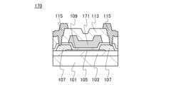
図5(A)乃至図5(C)に、トランジスタ100の上面図及び断面図を示す。図5(A
)はトランジスタ100の上面図であり、図5(B)は、図5(A)の一点鎖線A-B間
の断面図であり、図5(C)は、図5(A)の一点鎖線C-D間の断面図である。なお、
図5(A)では、明瞭化のため、トランジスタ100の構成要素の一部(例えば、基板1
01、下地絶縁膜103、ゲート絶縁膜109)、保護膜113などを省略している。5A to 5C are top views and cross-sectional views of the
5B is a cross-sectional view taken along dashed line A-B in FIG. 5A, and FIG. 5C is a cross-sectional view taken along dashed line C-D in FIG. 5A.
In FIG. 5A, for clarity, some of the components of the transistor 100 (e.g., the
1, the insulating
図5(B)及び図5(C)に示すトランジスタ100は、下地絶縁膜103上に形成され
る酸化物半導体膜105と、酸化物半導体膜105に接する一対の電極107と、下地絶
縁膜103、酸化物半導体膜105、及び一対の電極107に接するゲート絶縁膜109
と、ゲート絶縁膜109を介して酸化物半導体膜105と重なるゲート電極111とを有
する。また、ゲート絶縁膜109及びゲート電極111を覆う保護膜113と、ゲート絶
縁膜109及び保護膜113の開口部110(図5(A)参照。)において、一対の電極
107と接する配線115とを有してもよい。The
and a
本実施の形態に示すトランジスタ100上に設けられる保護膜113が、化学量論的組成
を満たす酸素よりも多くの酸素を含む酸化絶縁膜である。さらに好ましくは、保護膜11
3は、酸化物半導体膜105に含まれる酸素欠損量以上の酸素を含む。化学量論的組成を
満たす酸素よりも多くの酸素を含む酸化絶縁膜は、加熱により酸素の一部が脱離する酸化
絶縁膜である。このため、加熱により酸素の一部が脱離する酸化絶縁膜を保護膜113と
して設けることで、加熱処理により酸化物半導体膜105に酸素を拡散させ、酸化物半導
体膜105に含まれる酸素欠損を補填することが可能である。この結果、酸化物半導体膜
105に含まれる酸素欠損量が低減され、しきい値電圧のマイナスシフトを抑制したトラ
ンジスタとなる。また、経時変化や光ゲートBTストレス試験によって、しきい値電圧の
変動が少なく、優れた電気特性を有するトランジスタとなる。The
3 contains oxygen equal to or greater than the amount of oxygen vacancies contained in the
なお、トランジスタ100においては、保護膜113に含まれる酸素は、下地絶縁膜10
3及びゲート絶縁膜109の一以上を介して、酸化物半導体膜105に移動する。In the
The impurity ions are transferred to the
また、保護膜113において、電子スピン共鳴測定によるg=2.001に現れる信号の
スピン密度が1.5×10¹⁸spins/cm3未満、好ましくは1.0×1018s
pins/cm3以下であると、優れた電気特性を有するトランジスタとなるため好まし
い。In the
A density of 1000 ns/cm3 or less is preferable because it results in a transistor having excellent electrical characteristics.
保護膜113としては、厚さが30nm以上500nm以下、好ましくは100nm以上
400nm以下の酸化シリコン膜、酸化窒化シリコン膜等を用いることができる。The
以下に、トランジスタ100の他の構成の詳細について説明する。Other configurations of the
基板101は、実施の形態1に示す基板11に列挙する基板を適宜用いることができる。The
下地絶縁膜103は、加熱により酸素の一部が脱離する酸化絶縁膜を用いて形成すること
が好ましい。加熱により酸素の一部が脱離する酸化絶縁膜としては、化学量論的組成を満
たす酸素よりも多くの酸素を含む酸化絶縁膜を用いることが好ましい。加熱により酸素の
一部が脱離する酸化絶縁膜は、加熱処理により酸化物半導体膜に酸素を拡散させることが
できる。下地絶縁膜103の代表例としては、酸化シリコン、酸化窒化シリコン、窒化酸
化シリコン、酸化ガリウム、酸化ハフニウム、酸化イットリウム、酸化アルミニウム、酸
化窒化アルミニウム等がある。The base
下地絶縁膜103は、50nm以上、好ましくは200nm以上3000nm以下、好ま
しくは300nm以上1000nm以下とする。下地絶縁膜103を厚くすることで、下
地絶縁膜103の酸素脱離量を増加させることができると共に、下地絶縁膜103及び後
に形成される酸化物半導体膜との界面における界面準位を低減することが可能である。The thickness of the
ここで、「加熱により酸素の一部が脱離する」とは、TDS(Thermal Deso
rption Spectroscopy:昇温脱離ガス分光法)分析にて、酸素原子に
換算しての酸素の脱離量が1.0×10¹⁸atoms/cm3以上、好ましくは3.0
×1020atoms/cm3以上であることをいう。Here, "a part of oxygen is desorbed by heating" means that TDS (Thermal Desorption
In a thermal desorption spectroscopy (TGA) analysis, the amount of desorption of oxygen converted into oxygen atoms is 1.0×10¹⁸ atoms/cm3 or more, preferably 3.0
×1020 atoms/cm3 or more.
上記構成において、加熱により酸素の一部が脱離する絶縁膜は、酸素が過剰な酸化シリコ
ン(SiOX(X>2))であってもよい。酸素が過剰な酸化シリコン(SiOX(X>
2))とは、シリコン原子数の2倍より多い酸素原子を単位体積当たりに含むものである
。単位体積当たりのシリコン原子数及び酸素原子数は、ラザフォード後方散乱法により測
定した値である。In the above-described structure, the insulating film from which part of the oxygen is releasedby heating may be silicon oxide having an excess of oxygen (SiOx (X>2)).
2)) refers to a material containing more than twice as many oxygen atoms as silicon atoms per unit volume. The numbers of silicon atoms and oxygen atoms per unit volume are values measured by Rutherford backscattering spectrometry.
ここで、TDS分析にて、酸素原子に換算しての酸素の脱離量の測定方法について、以下
に説明する。Here, a method for measuring the amount of released oxygen converted into oxygen atoms in the TDS analysis will be described below.
TDS分析したときの気体の脱離量は、スペクトルの積分値に比例する。このため、絶縁
膜のスペクトルの積分値と、標準試料の基準値に対する比とにより、気体の脱離量を計算
することができる。標準試料の基準値とは、所定の原子を含む試料の、スペクトルの積分
値に対する原子の密度の割合である。The amount of gas desorbed during TDS analysis is proportional to the integral value of the spectrum. Therefore, the amount of gas desorbed can be calculated from the ratio of the integral value of the spectrum of the insulating film to the reference value of the standard sample. The reference value of the standard sample is the ratio of the density of atoms to the integral value of the spectrum of a sample containing a specific atom.
例えば、標準試料である所定の密度の水素を含むシリコンウェハのTDS分析結果、及び
絶縁膜のTDS分析結果から、絶縁膜の酸素分子の脱離量(NO2)は、数式1で求める
ことができる。ここで、TDS分析で得られる質量数32で検出されるスペクトルの全て
が酸素分子由来と仮定する。質量数32のものとしてCH3OHがあるが、存在する可能
性が低いものとしてここでは考慮しない。また、酸素原子の同位体である質量数17の酸
素原子及び質量数18の酸素原子を含む酸素分子についても、自然界における存在比率が
極微量であるため考慮しない。For example, the amount of desorbed oxygen molecules (NO2 ) from the insulating film can be calculated from the TDS analysis results of a silicon wafer containing hydrogen at a predetermined density as a standard sample and the TDS analysis results of the insulating
NO2=NH2/SH2×SO2×α (数式1)NO2 =NH2 /SH2 ×SO2 × α (Formula 1)
NH2は、標準試料から脱離した水素分子を密度で換算した値である。SH2は、標準試
料をTDS分析したときのスペクトルの積分値である。ここで、標準試料の基準値を、N
H2/SH2とする。SO2は、絶縁膜をTDS分析したときのスペクトルの積分値であ
る。αは、TDS分析におけるスペクトル強度に影響する係数である。数式1の詳細に関
しては、特開平6-275697公報を参照する。なお、上記絶縁膜の酸素の脱離量は、
電子科学株式会社製の昇温脱離分析装置EMD-WA1000S/Wを用い、標準試料と
して1×10¹⁶atoms/cm2の水素原子を含むシリコンウェハを用いて測定する
。NH2 is the density of hydrogen molecules desorbed from the standard sample. SH2 is the integral value of the spectrum obtained when the standard sample is analyzed by TDS. Here, the reference value of the standard sample is N
H2 /SH2 . SO2 is the integral value of the spectrum when the insulating film is analyzed by TDS. α is a coefficient that affects the spectrum intensity in the TDS analysis. For details of the
The measurement is carried out using a thermal desorption analyzer EMD-WA1000S/W manufactured by Electro Scientific Co., Ltd., and using a silicon wafer containing hydrogen atoms at 1×10¹⁶ atoms/cm2 as a standard sample.
また、TDS分析において、酸素の一部は酸素原子として検出される。酸素分子と酸素原
子の比率は、酸素分子のイオン化率から算出することができる。なお、上述のαは酸素分
子のイオン化率を含むため、酸素分子の脱離量を評価することで、酸素原子の脱離量につ
いても見積もることができる。In addition, in the TDS analysis, a part of oxygen is detected as oxygen atoms. The ratio of oxygen molecules to oxygen atoms can be calculated from the ionization rate of oxygen molecules. Since the above-mentioned α includes the ionization rate of oxygen molecules, the amount of desorbed oxygen atoms can also be estimated by evaluating the amount of desorbed oxygen molecules.
なお、NO2は酸素分子の脱離量である。絶縁膜においては、酸素原子に換算したときの
酸素の脱離量は、酸素分子の脱離量の2倍となる。In addition,NO2 is the amount of released oxygen molecules. In the insulating film, the amount of released oxygen when converted into oxygen atoms is twice the amount of released oxygen molecules.
下地絶縁膜103から酸化物半導体膜105に酸素が供給されることで、下地絶縁膜10
3及び酸化物半導体膜105の界面準位を低減できる。この結果、トランジスタの動作な
どに起因して生じうる電荷などが、上述の下地絶縁膜103及び酸化物半導体膜105の
界面に捕獲されることを抑制することができ、電気特性の変動の少ないトランジスタを得
ることができる。Oxygen is supplied from the
This can reduce the interface state between the base
即ち、酸化物半導体膜105に酸素欠損が生じると、下地絶縁膜103と酸化物半導体膜
105との界面において電荷が捕獲され、当該電荷がトランジスタの電気特性に影響して
しまうところ、下地絶縁膜103として、加熱により酸素が脱離する絶縁膜を設けること
で、酸化物半導体膜105及び下地絶縁膜103の界面準位を低減し、酸化物半導体膜1
05及び下地絶縁膜103の界面における電荷捕獲の影響を小さくすることができる。That is, when oxygen vacancies occur in the
The influence of charge trapping at the interface between the insulating
酸化物半導体膜105は、実施の形態1に示す酸化物半導体膜19と同様に形成すること
ができる。The
一対の電極107は、実施の形態1に示す一対の電極21と同様に形成することができる
。なお、一対の電極107において、チャネル幅方向における長さが酸化物半導体膜10
5より長く、更にはチャネル長方向と交差する端部を覆う構造とし、一対の電極107及
び酸化物半導体膜105の接触面積を増大させることで、酸化物半導体膜105と一対の
電極107との接触抵抗を低減することが可能であり、トランジスタのオン電流を高める
ことができる。The pair of
5 and further covering the ends intersecting the channel length direction, thereby increasing the contact area between the pair of
なお、ここでは、一対の電極107は、酸化物半導体膜105及びゲート絶縁膜109の
間に設けられているが、下地絶縁膜103及び酸化物半導体膜105の間に一対の電極1
07を設けてもよい。Note that although the pair of
07 may also be provided.
ゲート絶縁膜109は、実施の形態1に示すゲート絶縁膜17と同様に形成することがで
きる。The
ゲート電極111は、実施の形態1に示すゲート電極15と同様に形成することができる
。The
配線115は、一対の電極107に列挙する材料を適宜用いることができる。The
次に、図5に示すトランジスタの作製方法について、図6を用いて説明する。Next, the method for manufacturing the transistor shown in Figure 5 will be explained using Figure 6.
図6(A)に示すように、基板101上に下地絶縁膜103を形成する。次に、下地絶縁
膜103上に酸化物半導体膜105を形成する。6A, a
下地絶縁膜103は、スパッタリング法、CVD法等により形成する。The base
下地絶縁膜103として、加熱により酸素の一部が脱離する酸化絶縁膜をスパッタリング
法により形成する場合は、成膜ガス中の酸素量が高いことが好ましく、酸素、または酸素
及び希ガスの混合ガス等を用いることができる。代表的には、成膜ガス中の酸素濃度を6
%以上100%以下にすることが好ましい。In the case where an oxide insulating film from which part of oxygen is released by heating is formed as the
It is preferable that the ratio is 100% or more and 100% or less.
また、下地絶縁膜103としてCVD法で酸化絶縁膜を形成する場合、原料ガス由来の水
素または水が酸化絶縁膜中に混入される場合がある。このため、CVD法で酸化絶縁膜を
形成した後、脱水素化または脱水化として、加熱処理を行うことが好ましい。In the case where an oxide insulating film is formed as the
さらに、CVD法で形成した酸化絶縁膜に、酸素を導入することで、加熱により脱離する
酸素量を増加させることができる。酸化絶縁膜に酸素を導入する方法としては、イオン注
入法、イオンドーピング法、プラズマイマージョンイオンインプランテーション法、プラ
ズマ処理等がある。Furthermore, by introducing oxygen into an oxide insulating film formed by a CVD method, the amount of oxygen released by heating can be increased. Methods for introducing oxygen into an oxide insulating film include ion implantation, ion doping, plasma immersion ion implantation, plasma treatment, and the like.
ここで、酸化物半導体膜105は、実施の形態1に示す酸化物半導体膜19と同様の形成
方法を適宜用いることができる。Here, the
また、CAAC-OS膜に含まれる結晶部の配向を高めるためには、酸化物半導体膜の下
地絶縁膜である、下地絶縁膜103の表面の平坦性を高めることが好ましい。代表的には
、下地絶縁膜103の平均面粗さ(Ra)を、1nm以下、0.3nm以下、または0.
1nm以下とすることが好ましい。なお、本明細書等において、平均面粗さ(Ra)とは
、JISB0601:2001(ISO4287:1997)で定義されている算術平均
粗さを、曲面に対して適用できるよう三次元に拡張したものであり、基準面から指定面ま
での偏差の絶対値を平均した値で表現される。また、平坦化処理としては、化学的機械的
研磨(Chemical Mechanical Polishing:CMP)処理、
ドライエッチング処理、真空のチャンバーに不活性ガス、例えばアルゴンガスを導入し、
被処理面を陰極とする電界をかけて、表面の微細な凹凸を平坦化するプラズマ処理(いわ
ゆる逆スパッタ)等の一または複数を適用することができる。In order to improve the orientation of crystal parts in the CAAC-OS film, it is preferable to increase the flatness of the surface of the
It is preferable that the surface roughness is 1 nm or less. In this specification, the average surface roughness (Ra) is a three-dimensional extension of the arithmetic mean roughness defined in JIS B0601:2001 (ISO 4287:1997) so that it can be applied to curved surfaces, and is expressed as an average value of the absolute deviation from a reference surface to a specified surface. In addition, examples of the planarization process include chemical mechanical polishing (CMP) process,
Dry etching process: Inert gas, such as argon gas, is introduced into a vacuum chamber.
One or more of the following treatments can be applied: plasma treatment (so-called reverse sputtering) in which an electric field is applied with the surface to be treated as the cathode to flatten fine irregularities on the surface.
次に、加熱処理を行うことが好ましい。当該加熱処理により、下地絶縁膜103に含まれ
る酸素の一部を、下地絶縁膜103及び酸化物半導体膜105の界面近傍に拡散させるこ
とができる。この結果、下地絶縁膜103及び酸化物半導体膜105の界面近傍における
界面準位を低減することができる。Next, heat treatment is preferably performed. By the heat treatment, part of oxygen contained in the
加熱処理の温度は、代表的には、150℃以上基板歪み点未満、好ましくは250℃以上
450℃以下、更に好ましくは300℃以上450℃以下とする。The temperature of the heat treatment is typically 150° C. or higher and lower than the substrate distortion point, preferably 250° C. or higher and 450° C. or lower, and more preferably 300° C. or higher and 450° C. or lower.
加熱処理は、ヘリウム、ネオン、アルゴン、キセノン、クリプトン等の希ガス、または窒
素を含む不活性ガス雰囲気で行う。または、不活性ガス雰囲気で加熱した後、酸素雰囲気
で加熱してもよい。なお、上記不活性雰囲気及び酸素雰囲気に水素、水などが含まれない
ことが好ましい。処理時間は3分~24時間とする。The heat treatment is performed in an inert gas atmosphere containing nitrogen or a rare gas such as helium, neon, argon, xenon, or krypton. Alternatively, the heat treatment may be performed in an inert gas atmosphere and then in an oxygen atmosphere. Note that it is preferable that the inert atmosphere and the oxygen atmosphere do not contain hydrogen, water, or the like. The treatment time is 3 minutes to 24 hours.
なお、後に酸化物半導体膜105となる酸化物半導体膜を下地絶縁膜103上に形成し、
上記加熱処理を行った後、該酸化物半導体膜の一部をエッチングして、酸化物半導体膜1
05を形成してもよい。当該工程により、下地絶縁膜103に含まれる酸素において、よ
り多くの酸素を下地絶縁膜103及び酸化物半導体膜105の界面近傍に拡散させること
ができる。Note that an oxide semiconductor film which will later become the
After the heat treatment, a part of the oxide semiconductor film is etched to obtain an
Through this step, more oxygen contained in the
次に、図6(B)に示すように、一対の電極107を形成する。一対の電極107は実施
の形態1に示す一対の電極21と同様の形成方法を適宜用いることができる。または、印
刷法またはインクジェット法により一対の電極107を形成することができる。6B, a pair of
次に、図6(C)に示すように、ゲート絶縁膜109を形成した後、ゲート絶縁膜109
上にゲート電極111を形成する。Next, as shown in FIG. 6C, after forming the
A
ゲート絶縁膜109は、実施の形態1に示すゲート絶縁膜17と同様の形成方法を適宜用
いることができる。The
また、CAAC-OS膜は、被形成面または表面に沿って酸素が移動しやすい。このため
、素子分離した酸化物半導体膜105の側面から酸素の脱離が生じやすく、酸素欠損が形
成されやすい。しかしながら、酸化物半導体膜105上に加熱により酸素の一部が脱離す
る酸化絶縁膜と、当該酸化絶縁膜上に金属酸化膜とをゲート絶縁膜109として設けるこ
とにより、酸化物半導体膜105の側面からの酸素脱離を抑制することが可能である。こ
の結果、酸化物半導体膜105の側面の導電性の上昇を抑制することを抑制することがで
きる。In addition, oxygen easily moves along the surface or the top surface of the CAAC-OS film. Thus, oxygen is easily released from the side surface of the
ゲート電極111は、実施の形態1に示すゲート電極15の形成方法を適宜用いることが
できる。The
ここで、露光装置の解像限界以下の幅にまで微細化されたゲート電極の形成方法の一例に
ついて説明する。ゲート電極111の形成に用いるマスクに対してスリミング処理を行い
、より微細な構造のマスクとすることが好ましい。スリミング処理としては、例えば、酸
素ラジカルなどを用いるアッシング処理を適用することができる。ただし、スリミング処
理はフォトリソグラフィ法などによって形成されたマスクをより微細な構造に加工できる
処理であれば、アッシング処理以外の方法を用いてもよい。また、スリミング処理によっ
て形成されるマスクによって、トランジスタのチャネル長が決定されることになるため、
制御性の良好な処理を適用することが好ましい。スリミング処理の結果、フォトリソグラ
フィ法などによって形成されたマスクを、露光装置の解像限界以下、好ましくは、1/2
以下、より好ましくは1/3以下の幅にまで微細化することが可能である。例えば、形成
されたマスクの幅は、20nm以上2000nm以下、好ましくは50nm以上350n
m以下を達成することができる。また、スリミングしたマスクを後退させながら、導電膜
をエッチングすることで、露光装置の解像限界以下の幅にまで微細化されたゲート電極1
11を形成することができる。Here, an example of a method for forming a gate electrode that has been miniaturized to a width equal to or smaller than the resolution limit of an exposure device will be described. It is preferable to perform a slimming process on the mask used to form the
It is preferable to apply a process with good controllability. As a result of the slimming process, the mask formed by the photolithography method or the like is slimmed to a size smaller than the resolution limit of the exposure device, preferably 1/2.
For example, the width of the formed mask can be 20 nm to 2000 nm, preferably 50 nm to 350 nm.
In addition, by etching the conductive film while retracting the slimmed mask, the
11 can be formed.
次に、図6(D)に示すように、ゲート絶縁膜109及びゲート電極111上に保護膜1
13を形成した後、一対の電極107に接続する配線115を形成する。Next, as shown in FIG. 6D, a
After forming the insulating
保護膜113は、実施の形態1に示す保護膜23と同様に、プラズマCVD装置の真空排
気された処理室内に載置された基板101を180℃以上260℃以下、好ましくは18
0℃以上250℃以下、さらに好ましくは180℃以上230℃以下に保持し、処理室に
原料ガスを導入して処理室内における圧力を100Pa以上250Pa以下、さらに好ま
しくは100Pa以上200Pa以下とし、処理室内に設けられる電極に0.17W/c
m2以上0.5W/cm2以下、好ましくは0.25W/cm2以上0.40W/cm2
以下、さらに好ましくは0.26W/cm2以上0.35W/cm2以下の高周波電力を
供給する条件により、酸化シリコン膜または酸化窒化シリコン膜を形成する。The
The temperature is kept at 0° C. or higher and 250° C. or lower, more preferably 180° C. or higher and 230° C. or lower, a source gas is introduced into the processing chamber to adjust the pressure in the processing chamber to 100 Pa or higher and 250 Pa or lower, more preferably 100 Pa or higher and 200 Pa or lower, and a power of 0.17 W/cm is applied to an electrode provided in the processing chamber.
m2 ormore and 0.5 W/cm2 orless , preferably 0.25 W/cm2 ormore and 0.40 W/cm2or less
More preferably, a silicon oxide film or a silicon oxynitride film is formed under conditions in which high frequency power of 0.26 W/cm2 or more and 0.35 W/cm2 or less is supplied.
保護膜113の成膜条件として、上記圧力において上記パワー密度の高周波電力を供給す
ることで、化学量論的組成を満たす酸素よりも多くの酸素を含む酸化絶縁膜を形成するこ
とができる。As the deposition conditions for the
次に、実施の形態1と同様に、加熱処理を行うことで、保護膜113に含まれる酸素を酸
化物半導体膜105に拡散させ、酸化物半導体膜105に含まれる酸素欠損を補填するこ
とで、酸化物半導体膜105に含まれる酸素欠損量を低減することができる。また、保護
膜113形成後の加熱処理により、保護膜113の電子スピン共鳴測定によるg=2.0
01に現れる信号のスピン密度が1.5×10¹⁸spins/cm3未満、好ましくは
1.0×10¹⁸spins/cm3以下となる。該加熱処理の温度は、代表的には、1
50℃以上基板歪み点未満、好ましくは250℃以上450℃以下、更に好ましくは30
0℃以上450℃以下とする。Next, in a manner similar to that of
The spin density of the signal appearing in the sample at 01 is less than 1.5×10¹⁸ spins/cm3 , and preferably 1.0×10¹⁸ spins/cm3 or less.
50° C. or higher and lower than the substrate distortion point, preferably 250° C. or higher and 450° C. or lower, more preferably 30
The temperature is from 0°C to 450°C.
配線115は、スパッタリング法、CVD法、蒸着法等で導電膜を形成した後、該導電膜
上にマスクを形成して導電膜をエッチングして形成する。導電膜上に形成するマスクは、
印刷法、インクジェット法、フォトリソグラフィ法を適宜用いることができる。この後マ
スクを除去する。また、配線115をデュアルダマシン法で形成してもよい。The
A printing method, an ink jet method, or a photolithography method can be appropriately used. After that, the mask is removed. The
以上の工程により、しきい値電圧のマイナスシフトを抑制した、優れた電気特性を有する
トランジスタを作製することができる。また、経時変化や光ゲートBTストレス試験によ
る電気特性の変動の少ない、信頼性の高いトランジスタを作製することができる。Through the above steps, a transistor having excellent electrical characteristics and suppressing a negative shift in threshold voltage can be manufactured. In addition, a highly reliable transistor having little change in electrical characteristics due to aging or a light-gate BT stress test can be manufactured.
なお、本実施の形態に示す構成及び方法などは、他の実施の形態及び実施例に示す構成及
び方法などと適宜組み合わせて用いることができる。Note that the structures and methods described in this embodiment mode can be used in appropriate combination with structures and methods described in other embodiment modes and examples.
(実施の形態3)
本実施の形態では、実施の形態1及び実施の形態2と異なる構造のトランジスタについて
、図7を用いて説明する。本実施の形態に示すトランジスタ120は、実施の形態2に示
すトランジスタ100と比較して、酸化物半導体膜にドーパントが添加されている点が異
なる。(Embodiment 3)
In this embodiment, a transistor having a structure different from those in
図7(A)及び図7(B)に、トランジスタ120の上面図及び断面図を示す。図7(A
)はトランジスタ120の上面図であり、図7(B)は、図7(A)の一点鎖線A-B間
の断面図である。なお、図7(A)では、明瞭化のため、トランジスタ120の構成要素
の一部(例えば、基板101、下地絶縁膜103、ゲート絶縁膜109)、保護膜113
などを省略している。7A and 7B are a top view and a cross-sectional view of the
7B is a cross-sectional view taken along dashed line A-B in FIG. 7A. Note that in FIG. 7A, for clarity, some of the components of the transistor 120 (e.g., the
etc. are omitted.
図7(B)に示すトランジスタ120は、下地絶縁膜103上に形成される酸化物半導体
膜121と、酸化物半導体膜121に接する一対の電極107と、下地絶縁膜103、酸
化物半導体膜121、及び一対の電極107に接するゲート絶縁膜109と、ゲート絶縁
膜109を介して酸化物半導体膜121と重なるゲート電極111とを有する。また、ゲ
ート絶縁膜109及びゲート電極111を覆う保護膜113を有する。また、ゲート絶縁
膜109及び保護膜113の開口部110(図7(A)参照。)において、一対の電極1
07と接する配線115とを有してもよい。7B includes an
07 and a
本実施の形態に示すトランジスタ120は、酸化物半導体膜121において、ゲート電極
111とゲート絶縁膜109を介して重なる第1の領域123と、ドーパントが添加され
た第2の領域125と、一対の電極107と接する第3の領域127とを有する。なお、
第1の領域123及び第3の領域127には、ドーパントが添加されていない。第1の領
域123を挟むように対となる第2の領域125が設けられる。また、第1の領域123
及び第2の領域125を間に挟むように対となる第3の領域127が設けられる。The
The
A
第1の領域123は、トランジスタ120においてチャネル領域として機能する。第3の
領域127において一対の電極107と接する領域は、一対の電極107によって酸素の
一部が一対の電極107に拡散し、酸素欠損ができ、n型化する。このため、第3の領域
127の一部はソース領域及びドレイン領域として機能する。第2の領域は、ドーパント
が添加され、導電率が高いため、低抵抗領域として機能し、チャネル領域と、ソース領域
及びドレイン領域との間の抵抗を低減することができる。このため、実施の形態1に示す
トランジスタ100と比較して、トランジスタ120のオン電流及び電界効果移動度を高
めることができる。The
第2の領域125に添加されるドーパントとしては、ホウ素、窒素、リン、及びヒ素の少
なくとも一以上がある。または、ヘリウム、ネオン、アルゴン、クリプトン、及びキセノ
ンの少なくとも一以上がある。なお、ドーパントとして、ホウ素、窒素、リン、及びヒ素
の一以上と、ヘリウム、ネオン、アルゴン、クリプトン、及びキセノンの一以上とが適宜
組み合わされて含まれていてもよい。The dopant added to the
また、第2の領域125に含まれるドーパントの濃度は、5×10¹⁸atoms/cm
3以上1×10²²atoms/cm3以下、好ましくは5×1018atoms/cm
3以上5×10¹⁹atoms/cm3未満とする。The concentration of the dopant contained in the
3 or more and 1×10²² atoms/cm3 or less, preferably 5×10¹⁸ atoms/cm
The concentration is set to3 or more and less than 5×10¹⁹ atoms/cm3 .
第2の領域125はドーパントを含むため、キャリア密度または欠陥を増加させることが
できる。このため、ドーパントを含まない第1の領域123及び第3の領域127と比較
して導電性を高めることができる。なお、ドーパント濃度を増加させすぎると、ドーパン
トがキャリアの移動を阻害することになり、第2の領域125の導電性を低下させること
になる。Since the
第2の領域125は、導電率が0.1S/cm以上1000S/cm以下、好ましくは1
0S/cm以上1000S/cm以下とすることが好ましい。The
It is preferable that the resistivity is 0 S/cm or more and 1000 S/cm or less.
次に、本実施の形態に示すトランジスタ120の作製方法について、図6及び図7を用い
て説明する。Next, a manufacturing method of the
実施の形態1と同様に、図6(A)乃至図6(C)の工程を経て、基板101上に下地絶
縁膜103を形成し、下地絶縁膜103上に酸化物半導体膜121を形成し、酸化物半導
体膜121上に一対の電極107を形成する。次に、酸化物半導体膜121及び一対の電
極107上にゲート絶縁膜109を形成し、ゲート絶縁膜109を介して、酸化物半導体
膜121の一部と重なるように、ゲート電極111を形成する。6A to 6C, a
次に、一対の電極107及びゲート電極111をマスクとして、酸化物半導体膜121に
ドーパントを添加する。酸化物半導体膜121にドーパントを添加する方法として、イオ
ンドーピング法またはイオンインプランテーション法を用いることができる。Next, by using the pair of
また、上記酸化物半導体膜121へのドーパントの添加は、酸化物半導体膜121を覆っ
て、ゲート絶縁膜109が形成されている状態を示したが、酸化物半導体膜121が露出
している状態でドーパントの添加を行ってもよい。Although the dopant is added to the
さらに、上記ドーパントの添加はイオンドーピング法またはイオンインプランテーション
法などによる注入以外の方法でも行うことができる。例えば、添加する元素を含むガス雰
囲気にてプラズマを発生させて、酸化物半導体膜121に対してプラズマ処理を行うこと
によって、ドーパントを添加することができる。上記プラズマを発生させる装置としては
、ドライエッチング装置、プラズマCVD装置などを用いることができる。Furthermore, the dopant can be added by a method other than injection by an ion doping method or an ion implantation method. For example, the dopant can be added by generating plasma in a gas atmosphere containing an element to be added and performing a plasma treatment on the
なお、ドーパントの添加処理は、基板101を加熱しながら行ってもよい。The dopant addition process may be performed while heating the
ここでは、イオンインプランテーション法により、リンを酸化物半導体膜121に添加す
る。Here, phosphorus is added to the
この後、加熱処理を行う。当該加熱処理の温度は、代表的には、150℃以上450℃以
下、好ましくは250℃以上325℃以下とする。または、250℃から325℃まで徐
々に温度上昇させながら加熱してもよい。After that, a heat treatment is performed at a temperature of typically 150° C. to 450° C., preferably 250° C. to 325° C. Alternatively, the temperature may be gradually increased from 250° C. to 325° C.
当該加熱処理により、第2の領域125の導電率を高めることができる。なお、当該加熱
処理において、第1の領域123、第2の領域125,及び第3の領域127は、多結晶
構造、非晶質構造、またはCAAC-OSとなる。This heat treatment can increase the electrical conductivity of the
こののち、実施の形態1と同様に、保護膜113を形成し、加熱処理して保護膜113に
含まれる酸素を酸化物半導体膜121に拡散させ、酸化物半導体膜121の酸素欠損を低
減した後、配線115を形成して、図7に示すトランジスタ120を形成することができ
る。After that, in a manner similar to that of
本実施の形態に示すトランジスタ120は、酸化物半導体膜121において、チャネル領
域となる第1の領域123と、ソース領域及びドレイン領域として機能する第3の領域1
27の間に、低抵抗領域である第2の領域125を有する。このため、実施の形態2に示
すトランジスタ100と比較して、チャネル領域と、ソース領域及びドレイン領域との間
の抵抗を低減することが可能であり、オン電流を高めたトランジスタを作製することがで
きる。また、トランジスタ120上に保護膜113を設けることで、しきい値電圧のマイ
ナスシフトを抑制した、優れた電気特性を有するトランジスタを作製することができる。
また、経時変化や光ゲートBTストレス試験による電気特性の変動の少ない、信頼性の高
いトランジスタを作製することができる。The
27, the
In addition, a highly reliable transistor in which changes in electrical characteristics over time or due to a light gate BT stress test are small can be manufactured.
なお、トランジスタ120においては、保護膜113に含まれる酸素は、下地絶縁膜10
3及びゲート絶縁膜109の一以上を介して、酸化物半導体膜121に移動する。In the
The
なお、本実施の形態に示す構成及び方法などは、他の実施の形態及び実施例に示す構成及
び方法などと適宜組み合わせて用いることができる。Note that the structures and methods described in this embodiment mode can be used in appropriate combination with structures and methods described in other embodiment modes and examples.
(実施の形態4)
本実施の形態では、実施の形態1乃至実施の形態3と異なる構造のトランジスタについて
、図8を用いて説明する。本実施の形態に示すトランジスタ130は、他の実施の形態に
示すトランジスタと比較して、酸化物半導体膜の構造が異なり、チャネル領域と、ソース
領域及びドレイン領域との間に、電界緩和領域を有する。(Embodiment 4)
In this embodiment, a transistor having a structure different from those in
図8(A)及び図8(B)に、トランジスタ130の上面図及び断面図を示す。図8(A
)はトランジスタ130の上面図であり、図8(B)は、図8(A)の一点鎖線A-B間
の断面図である。なお、図8(A)では、明瞭化のため、トランジスタ130の構成要素
の一部(例えば、基板101、下地絶縁膜103、ゲート絶縁膜109)、保護膜113
などを省略している。8A and 8B are a top view and a cross-sectional view of the
8A is a top view of the
etc. are omitted.
図8(B)に示すトランジスタ130は、基板101上に設けられる下地絶縁膜103と
、下地絶縁膜103上に形成される酸化物半導体膜131と、酸化物半導体膜131に接
する一対の電極139と、下地絶縁膜103、酸化物半導体膜131、及び一対の電極1
39に接するゲート絶縁膜109と、ゲート絶縁膜109を介して酸化物半導体膜131
と重なるゲート電極111とを有する。また、ゲート絶縁膜109及びゲート電極111
を覆う保護膜113を有する。また、ゲート絶縁膜109及び保護膜113の開口部11
0において、一対の電極139と接する配線115とを有してもよい。The
39 and the
The
The
0, a pair of
本実施の形態に示すトランジスタ130は、酸化物半導体膜131において、ゲート電極
111とゲート絶縁膜109を介して重なる第1の領域133と、ドーパントが添加され
た第2の領域135と、一対の電極139と接し、且つドーパントが添加された第3の領
域137とを有する。なお、第1の領域133には、ドーパントが添加されていない。第
1の領域133を挟むように対となる第2の領域135が設けられる。また、第1の領域
133及び第2の領域135を間に挟むように対となる第3の領域137が設けられる。The
第2の領域135及び第3の領域137に添加されるドーパントとしては、実施の形態3
に示す第2の領域125と同様のドーパントを適宜用いることができる。The dopants added to the
The same dopant as that for the
また、第2の領域135及び第3の領域137に含まれるドーパントの濃度及び導電率は
、実施の形態3に示す第2の領域125と同様のドーパントの濃度とすることができる。
なお、本実施の形態においては、第2の領域135より第3の領域137の方がドーパン
トの濃度及び導電率が高い。The concentration and electrical conductivity of the dopant contained in the
In this embodiment, the
第1の領域133は、トランジスタ130においてチャネル領域として機能する。第2の
領域135は、電界緩和領域として機能する。第3の領域137において一対の電極13
9と接する領域は、一対の電極139の材料によっては酸素の一部が一対の電極139に
拡散し、酸素欠損ができ、n型化する。また、第3の領域137にはドーパントが添加さ
れ、導電率が高いため、実施の形態2に示すトランジスタ120と比較して、第3の領域
137及び一対の電極139のコンタクト抵抗をさらに低減することができる。このため
、実施の形態2に示すトランジスタと比較して、トランジスタ130は、オン電流及び電
界効果移動度を高めることができる。The
In the region in contact with the
なお、一対の電極139は、第3の領域137にドーパントを添加させるために、膜厚を
薄くすることが好ましく、代表的には、10nm以上100nm以下、好ましくは20n
m以上50nm以下とする。In order to add a dopant to the
The thickness is set to be m or more and 50 nm or less.
次に、本実施の形態に示すトランジスタ130の作製方法について、図6及び図8を用い
て説明する。Next, a manufacturing method of the
実施の形態2と同様に、図6(A)乃至図6(C)の工程を経て、基板101上に下地絶
縁膜103を形成し、下地絶縁膜103上に酸化物半導体膜131を形成し、酸化物半導
体膜131上に一対の電極139(図8(B)参照。)を形成する。次に、酸化物半導体
膜131及び一対の電極139上にゲート絶縁膜109を形成し、ゲート絶縁膜109を
介して、酸化物半導体膜131の一部と重なるように、ゲート電極111を形成する。6A to 6C, a
次に、ゲート電極111をマスクとして、酸化物半導体膜131にドーパントを添加する
。ドーパントの添加方法は、実施の形態2に示す方法を適宜用いることができる。なお、
本実施の形態では、第2の領域135と共に、第3の領域137にもドーパントを添加す
る。さらに、第2の領域135より第3の領域137の方がドーパントの濃度が高い。こ
のため、ドーパント濃度のプロファイルのピークが第3の領域137となるように、添加
方法の条件を適宜用いる。このとき、第3の領域137は一対の電極139と重なるが、
第2の領域135は、一対の電極139と重ならない。このため、第2の領域135では
、ドーパント濃度のプロファイルのピークが下地絶縁膜103となるため、第2の領域1
35におけるドーパントの濃度は、第3の領域137より低くなる。Next, a dopant is added to the
In this embodiment, a dopant is added to the
The
The concentration of dopant in 35 is less than that in the
この後、加熱処理を行う。当該加熱処理の温度は、代表的には、150℃以上450℃以
下、好ましくは250℃以上325℃以下とする。または、250℃から325℃まで徐
々に温度上昇させながら加熱してもよい。After that, a heat treatment is performed at a temperature of typically 150° C. to 450° C., preferably 250° C. to 325° C. Alternatively, the temperature may be gradually increased from 250° C. to 325° C.
当該加熱処理により、第2の領域135及び第3の領域137の導電率を高めることがで
きる。なお、当該加熱処理において、第1の領域133、第2の領域135、及び第3の
領域137は、多結晶構造、非晶質構造、またはCAAC-OSとなる。This heat treatment can increase the electrical conductivity of the
こののち、実施の形態2と同様に、保護膜113を形成し、加熱処理して保護膜113に
含まれる酸素を酸化物半導体膜131に拡散させ、酸素欠損量を低減させた後、配線11
5を形成して、図8に示すトランジスタ130を形成することができる。Thereafter, similarly to the second embodiment, the
5 to form the
本実施の形態に示すトランジスタ130は、酸化物半導体膜131において、チャネル領
域となる第1の領域133と、ソース領域及びドレイン領域として機能する第3の領域1
37の間に、電界緩和領域として機能する第2の領域135を有する。このため、実施の
形態2に示すトランジスタ100と比較して、トランジスタの劣化を抑制することができ
る。また、一対の電極139と接する第3の領域137にドーパントが含まれるため、一
対の電極139及び第3の領域137の接触抵抗をさらに低減することが可能であり、オ
ン電流を高めたトランジスタを作製することができる。また、トランジスタ130上に保
護膜113を設けることで、しきい値電圧のマイナスシフトを抑制した、優れた電気特性
を有するトランジスタを作製することができる。また、経時変化や光ゲートBTストレス
試験による電気特性の変動の少ない、信頼性の高いトランジスタを作製することができる
。The
37, the
なお、トランジスタ130においては、保護膜113に含まれる酸素は、下地絶縁膜10
3及びゲート絶縁膜109の一以上を介して、酸化物半導体膜131に移動する。In the
The
なお、本実施の形態に示す構成及び方法などは、他の実施の形態及び実施例に示す構成及
び方法などと適宜組み合わせて用いることができる。Note that the structures and methods described in this embodiment mode can be used in appropriate combination with structures and methods described in other embodiment modes and examples.
(実施の形態5)
本実施の形態では、実施の形態2乃至実施の形態4に適用可能なトランジスタの構造につ
いて、図9を用いて説明する。(Embodiment 5)
In this embodiment, a structure of a transistor applicable to any of
本実施の形態に示すトランジスタは、ゲート電極111の側面に接するサイドウォール絶
縁膜を有することを特徴とする。ここでは、実施の形態2に示すトランジスタを用いて説
明する。The transistor described in this embodiment has a feature that it has a sidewall insulating film in contact with a side surface of the
図9(A)に示すトランジスタ140は、下地絶縁膜103上に形成される酸化物半導体
膜105と、酸化物半導体膜105に接する一対の電極107と、下地絶縁膜103、酸
化物半導体膜105、及び一対の電極107に接するゲート絶縁膜109と、ゲート絶縁
膜109を介して酸化物半導体膜105と重なるゲート電極111とを有する。また、ゲ
ート電極111の側面に接するサイドウォール絶縁膜141を有する。ゲート絶縁膜10
9、ゲート電極111、及びサイドウォール絶縁膜141を覆う保護膜113を有する。
また、ゲート絶縁膜109及び保護膜113の開口部において、一対の電極107と接す
る配線115とを有してもよい。9A includes an
9, a
In addition,
サイドウォール絶縁膜141の端部は一対の電極107と重なり、一対の電極107及び
ゲート電極111の間を充填するように設けられている。一対の電極107及びゲート電
極111の間の凹凸を緩和することができる。このため、保護膜113の被覆率を高める
ことが可能である。Ends of the
図9(B)に示すトランジスタ150は、トランジスタ140と比較して、ゲート電極1
11の側面に接するサイドウォール絶縁膜151の形状が異なる。具体的には、サイドウ
ォール絶縁膜151の端部は、一対の電極107と重ならず、ゲート電極111及び一対
の電極107の間に位置する。The
The shape of a
図9(C)に示すトランジスタ160は、図9(B)に示すトランジスタ150と比較し
て、酸化物半導体膜161にドーパントが添加されている点が異なる。A
酸化物半導体膜161において、ゲート電極111とゲート絶縁膜109を介して重なる
第1の領域163と、ドーパントが添加され、且つサイドウォール絶縁膜151と重なる
第2の領域165と、ドーパントが添加された第3の領域167と、一対の電極107と
接する第4の領域169とを有する。なお、第1の領域163及び第4の領域169には
、ドーパントが添加されていない。第1の領域163を挟むように対となる第2の領域1
65が設けられる。また、第1の領域163及び第2の領域165を間に挟むように対と
なる第3の領域167が設けられる。また、第1の領域163乃至第3の領域167を間
に挟むように対となる第4の領域169が設けられる。The
65 is provided. A
第1の領域163は、トランジスタ160においてチャネル領域として機能する。The
第2の領域165及び第3の領域167は、ドーパントが添加され、導電率が高いため、
低抵抗領域として機能し、チャネル領域と、ソース領域及びドレイン領域との間の抵抗を
低減することができる。また、第2の領域165は第3の領域167よりドーパントの濃
度及び導電率が低いため、電界緩和領域として機能する。このため、トランジスタ160
の劣化を低減することができる。The
The
The deterioration of the material can be reduced.
第2の領域165及び第3の領域167に添加されるドーパントとしては、実施の形態3
に示す第2の領域125と同様のドーパントを適宜用いることができる。The dopants added to the
The same dopant as that for the
また、第2の領域165及び第3の領域167に含まれるドーパントの濃度、及び導電率
は、実施の形態3に示す第2の領域125と同様のドーパントの濃度とすることができる
。なお、本実施の形態においては、第2の領域165より第3の領域167の方がドーパ
ントの濃度及び導電率が高い。The dopant concentration and electrical conductivity of the
第4の領域169において一対の電極107と接する領域は、一対の電極107によって
は酸素の一部が一対の電極107に拡散し、酸素欠損ができ、n型化する。この結果、第
4の領域169の一部はソース領域及びドレイン領域として機能する。In the
本実施の形態に示すトランジスタ160は、酸化物半導体膜161において、第1の領域
163を挟むように、低抵抗領域である第2の領域165及び第3の領域167を有する
。このため、チャネル領域と、ソース領域及びドレイン領域との間の抵抗を低減すること
が可能であり、オン電流を高めたトランジスタを作製することができる。The
また、トランジスタ140、150、160上に保護膜113を設けることで、しきい値
電圧のマイナスシフトを抑制した、優れた電気特性を有するトランジスタを作製すること
ができる。また、経時変化や光ゲートBTストレス試験による電気特性の変動の少ない、
信頼性の高いトランジスタを作製することができる。In addition, by providing the
A highly reliable transistor can be manufactured.
なお、トランジスタ140、150、160においては、保護膜113に含まれる酸素は
、下地絶縁膜103、ゲート絶縁膜109の一以上を介して、酸化物半導体膜に移動する
。Note that in each of the
なお、本実施の形態に示す構成及び方法などは、他の実施の形態及び実施例に示す構成及
び方法などと適宜組み合わせて用いることができる。Note that the structures and methods described in this embodiment mode can be used in appropriate combination with structures and methods described in other embodiment modes and examples.
(実施の形態6)
本実施の形態では、実施の形態2乃至実施の形態5と異なる構造のトランジスタについて
、図10を用いて説明する。本実施の形態に示すトランジスタは、実施の形態2乃至実施
の形態5と比較して、一対の電極及びゲート電極がゲート絶縁膜を介して重なっている点
が異なる。(Embodiment 6)
In this embodiment, a transistor having a structure different from those in
図10に示すトランジスタ170は、下地絶縁膜103上に形成される酸化物半導体膜1
05と、酸化物半導体膜105に接する一対の電極107と、下地絶縁膜103、酸化物
半導体膜105、及び一対の電極107に接するゲート絶縁膜109と、ゲート絶縁膜1
09を介して酸化物半導体膜105と重なるゲート電極171とを有する。また、ゲート
絶縁膜109及びゲート電極171を覆う保護膜113を有する。また、ゲート絶縁膜1
09及び保護膜113の開口部において、一対の電極107と接する配線115とを有し
てもよい。The
105, a pair of
The
In the openings of the
本実施の形態に示すトランジスタ170は、一対の電極107及びゲート電極171がゲ
ート絶縁膜109を介して重なっている。このため、酸化物半導体膜105において、ゲ
ート絶縁膜109を介してゲート電極171と対向する領域がチャネル領域として機能し
、一対の電極107と接する領域がソース領域及びドレイン領域として機能する。即ち、
チャネル領域と、ソース領域及びドレイン領域とが接している。チャネル領域と、ソース
領域及びドレイン領域との間に抵抗となる領域がないため、実施の形態2乃至実施の形態
5に示すトランジスタと比較して、オン電流及び電界効果移動度が高い。In the
The channel region is in contact with the source region and the drain region, and since there is no region that acts as a resistance between the channel region and the source region and the drain region, the on-state current and the field-effect mobility are higher than those of the transistors described in any of
また、トランジスタ170上に保護膜113を設けることで、しきい値電圧のマイナスシ
フトを抑制した、優れた電気特性を有するトランジスタを作製することができる。また、
経時変化や光ゲートBTストレス試験による電気特性の変動の少ない、信頼性の高いトラ
ンジスタを作製することができる。In addition, by providing the
It is possible to manufacture a highly reliable transistor whose electrical characteristics are little changed over time or due to a light gate BT stress test.
なお、トランジスタ170においては、保護膜113に含まれる酸素は、下地絶縁膜10
3、ゲート絶縁膜109の一以上を介して、酸化物半導体膜105に移動する。In the
3. The electrons move to the
なお、本実施の形態に示す構成及び方法などは、他の実施の形態及び実施例に示す構成及
び方法などと適宜組み合わせて用いることができる。Note that the structures and methods described in this embodiment mode can be used in appropriate combination with structures and methods described in other embodiment modes and examples.
(実施の形態7)
本実施の形態では、実施の形態1乃至実施の形態6と異なる構造のトランジスタについて
、図11を用いて説明する。(Seventh embodiment)
In this embodiment, a transistor having a structure different from those in
図11(A)に示すトランジスタ210は、下地絶縁膜103上に形成される酸化物半導
体膜211と、下地絶縁膜103及び酸化物半導体膜211に接するゲート絶縁膜109
と、ゲート絶縁膜109を介して酸化物半導体膜211と重なるゲート電極111とを有
する。また、ゲート絶縁膜109及びゲート電極111を覆う保護膜217と、ゲート絶
縁膜109及び保護膜217の開口部において、酸化物半導体膜211と接する配線21
9を有する。A
and a
It has 9.
本実施の形態に示すトランジスタ210は、酸化物半導体膜211は、ゲート電極111
とゲート絶縁膜109を介して重なる第1の領域213と、ドーパントが添加された第2
の領域215とを有する。なお、第1の領域213には、ドーパントが添加されていない
。また、第1の領域213を挟むように対となる第2の領域215が設けられる。In the
A
The
第1の領域213は、トランジスタ210においてチャネル領域として機能する。第2の
領域215はソース領域及びドレイン領域として機能する。The
第2の領域215に添加されるドーパントとしては、実施の形態3に示す第2の領域12
5と同様のドーパントを適宜用いることができる。The dopant added to the
The same dopants as in 5 can be used appropriately.
また、第2の領域215に含まれるドーパントの濃度及び導電率は、実施の形態3に示す
第2の領域125と同様のドーパントの濃度とすることができる。The concentration of the dopant contained in the
図11(B)に示すトランジスタ220は、下地絶縁膜103上に設けられる酸化物半導
体膜211と、酸化物半導体膜211に接する、ソース電極及びドレイン電極として機能
する一対の電極225と、酸化物半導体膜211の少なくとも一部と接するゲート絶縁膜
223と、ゲート絶縁膜223上であって、且つ酸化物半導体膜211と重畳するゲート
電極111とを有する。A
また、ゲート電極111の側面に接するサイドウォール絶縁膜221を有する。また、下
地絶縁膜103、ゲート電極111、サイドウォール絶縁膜221、及び一対の電極22
5上に保護膜217を有する。また、保護膜217の開口部において、酸化物半導体膜2
11と接する配線219を有する。The
5. In addition, the
11. It has
図11(B)に示すトランジスタにおいて、酸化物半導体膜211は、ゲート電極111
とゲート絶縁膜223を介して重なる第1の領域213と、ドーパントが添加された第2
の領域215とを有する。なお、第1の領域213には、ドーパントが添加されていない
。第1の領域213を挟むように対となる第2の領域215が設けられる。In the transistor illustrated in FIG. 11B , the
A
The
トランジスタの一対の電極225の端部が、サイドウォール絶縁膜221上に位置し、更
に酸化物半導体膜211において、一対の電極225が、ドーパントを含む一対の第2の
領域215の露出部を全て覆っている。このため、チャネル長方向におけるソース-ドレ
イン間の距離(より正確には、一対の電極225と接する酸化物半導体膜211の間の距
離)を、サイドウォール絶縁膜221の幅で制御することができる。つまりマスクを用い
てパターンを形成するのが困難な微細なデバイスにおいて、酸化物半導体膜211と接す
る一対の電極225のチャネル側の端部を、マスクを用いずに形成させることができる。
また、マスクを使用しないため、複数のトランジスタにおける加工ばらつきを低減するこ
とができる。Ends of a pair of
Furthermore, since no mask is used, processing variations among a plurality of transistors can be reduced.
本実施の形態に示すトランジスタ210、220上に設けられる保護膜217は、実施の
形態1に示す保護膜23と同様に、化学量論的組成を満たす酸素よりも多くの酸素を含む
酸化絶縁膜である。さらに好ましくは、保護膜217は、酸化物半導体膜211に含まれ
る酸素欠損量以上の酸素を含む。化学量論的組成を満たす酸素よりも多くの酸素を含む酸
化絶縁膜は、加熱により酸素の一部が脱離する酸化絶縁膜である。このため、加熱により
酸素の一部が脱離する酸化絶縁膜を保護膜として設けることで、加熱処理により酸化物半
導体膜に酸素を拡散させ、酸化物半導体膜211に含まれる酸素欠損を補填することが可
能である。この結果、酸化物半導体膜211に含まれる酸素欠損量が低減され、しきい値
電圧のマイナスシフトを抑制したトランジスタとなる。また、経時変化や光ゲートBTス
トレス試験によって、しきい値電圧の変動が少なく、優れた電気特性を有するトランジス
タとなる。The
また、保護膜217において、電子スピン共鳴測定によるg=2.001に現れる信号の
スピン密度が1.5×10¹⁸spins/cm3未満、好ましくは1.0×1018s
pins/cm3以下であると、優れた電気特性を有するトランジスタとなるため好まし
い。In addition, in the
A density of 1000 ns/cm3 or less is preferable because it results in a transistor having excellent electrical characteristics.
なお、トランジスタ220においては、保護膜217に含まれる酸素は、下地絶縁膜10
3、ゲート絶縁膜223、及びサイドウォール絶縁膜221の一以上を介して、酸化物半
導体膜211に移動する。In the
3, the metal oxide moves to the
なお、本実施の形態に示す構成及び方法などは、他の実施の形態及び実施例に示す構成及
び方法などと適宜組み合わせて用いることができる。Note that the structures and methods described in this embodiment mode can be used in appropriate combination with structures and methods described in other embodiment modes and examples.
(実施の形態8)
本実施の形態では、実施の形態1乃至実施の形態7と異なる構造のトランジスタについて
、図12を用いて説明する。本実施の形態に示すトランジスタは、酸化物半導体膜を介し
て対向する複数のゲート電極を有することを特徴とする。なお、本実施の形態では、実施
の形態6に示すトランジスタを用いて説明するが、適宜他の実施の形態と組み合わせるこ
とができる。(Embodiment 8)
In this embodiment, a transistor having a structure different from those in
図12に示すトランジスタ230は、基板101上に設けられるゲート電極231と、ゲ
ート電極231を覆う絶縁膜233を有する。また、絶縁膜233上に形成される酸化物
半導体膜105と、酸化物半導体膜105に接する一対の電極107と、絶縁膜233、
酸化物半導体膜105、及び一対の電極107に接するゲート絶縁膜109と、ゲート絶
縁膜109を介して酸化物半導体膜105と重なるゲート電極171とを有する。また、
ゲート絶縁膜109及びゲート電極171を覆う保護膜113を有する。また、ゲート絶
縁膜109及び保護膜113の開口部において、一対の電極107と接する配線115と
を有してもよい。12 includes a
The
A
ゲート電極231は、実施の形態1に示すゲート電極15と同様に形成することができる
。なお、ゲート電極231は、後に形成される絶縁膜233の被覆性を高めるために、側
面がテーパ形状であることが好ましく、基板101とゲート電極231の側面のなす角度
は、20度以上70度以下、好ましくは30度以上60度以下とする。The
絶縁膜233は、実施の形態2に示す下地絶縁膜103と同様に形成することができる。
なお、後に、絶縁膜233上に酸化物半導体膜105を形成するため、絶縁膜233の表
面は平坦であることが好ましい。このため、後に絶縁膜233となる絶縁膜を基板101
及びゲート電極231上に形成した後、当該絶縁膜を平坦化処理して、表面の凹凸が少な
い絶縁膜233を形成する。The insulating
Note that the insulating
After being formed on the
本実施の形態に示すトランジスタ230は、酸化物半導体膜105を介して対向するゲー
ト電極231及びゲート電極171を有する。ゲート電極231とゲート電極171に異
なる電位を印加することで、トランジスタ230のしきい値電圧を制御し、好ましくは、
しきい値電圧をプラスシフトさせることができる。The
The threshold voltage can be shifted in the positive direction.
本実施の形態に示すトランジスタ230上に保護膜113が設けられる。保護膜113は
、実施の形態1に示す保護膜23と同様に、化学量論的組成を満たす酸素よりも多くの酸
素を含む酸化絶縁膜である。さらに好ましくは、保護膜113は、酸化物半導体膜105
に含まれる酸素欠損量以上の酸素を含む。この結果、酸化物半導体膜105に含まれる酸
素欠損量が低減され、しきい値電圧のマイナスシフトを抑制したトランジスタとなる。ま
た、経時変化や光ゲートBTストレス試験によって、しきい値電圧の変動が少なく、優れ
た電気特性を有するトランジスタとなる。A
As a result, the amount of oxygen vacancies in the
(実施の形態9)
本実施の形態では、実施の形態1乃至実施の形態8に示すトランジスタにおいて、酸化物
半導体膜中に含まれる水素濃度を低減したトランジスタの作製方法について説明する。こ
こでは、代表的に実施の形態1及び実施の形態2を用いて説明するが、適宜他の実施の形
態と組み合わせることができる。なお、本実施の形態に示す工程の一以上と、実施の形態
1及び実施の形態2に示すトランジスタの作製工程とが組み合わさればよく、全て組み合
わせる必要はない。(Embodiment 9)
In this embodiment, a method for manufacturing a transistor in which the hydrogen concentration in an oxide semiconductor film is reduced, which is one of the transistors described in
実施の形態1に示す酸化物半導体膜19及び実施の形態2に示す酸化物半導体膜105に
おいて、水素濃度を5×10¹⁹atoms/cm3未満、好ましくは5×1018at
oms/cm3未満、より好ましくは1×1018atoms/cm3以下、より好まし
くは5×10¹⁷atoms/cm3以下、さらに好ましくは1×1016atoms/
cm3以下とすることが好ましい。In the
less than 1×10¹⁸ atoms/cm3 , more preferably 1×10 18 atoms/cm3 or less, more preferably 5×10¹⁷ atoms/cm3 or less, and even more preferably 1×10¹⁶ atoms/
It is preferable to set the thickness to3 cm or less.
酸化物半導体膜19、105に含まれる水素は、金属原子と結合する酸素と反応して水と
なると共に、酸素が脱離した格子(あるいは酸素が脱離した部分)には欠損が形成されて
しまう。また、水素が酸素と結合することで、キャリアである電子が生じてしまう。これ
らのため、酸化物半導体膜の成膜工程において、水素を含む不純物を極めて減らすことに
より、酸化物半導体膜の水素濃度を低減することが可能である。このため、水素をできる
だけ除去し、高純度化させた酸化物半導体膜をチャネル領域とすることにより、しきい値
電圧のマイナスシフトを低減することができ、またトランジスタのソース及びドレインに
おけるリーク電流を、代表的には、チャネル幅あたりのオフ電流を数yA/μm~数zA
/μmにまで低減することが可能であり、トランジスタの電気特性を向上させることがで
きる。Hydrogen contained in the
/μm, and the electrical characteristics of the transistor can be improved.
酸化物半導体膜19中の水素濃度を低減する第1の方法として、酸化物半導体膜19を形
成する前に、加熱処理またはプラズマ処理により、基板11、下地絶縁膜13、ゲート電
極15、ゲート絶縁膜17それぞれに含まれる水素または水を脱離させる方法がある。こ
の結果、後の加熱処理において、基板11乃至ゲート絶縁膜17に付着または含有する水
素若しくは水が、酸化物半導体膜19中に拡散することを防ぐことができる。なお、加熱
処理は、不活性雰囲気、減圧雰囲気または乾燥空気雰囲気にて、100℃以上基板の歪み
点未満の温度で行う。また、プラズマ処理は、希ガス、酸素、窒素または酸化窒素(亜酸
化窒素、一酸化二窒素、二酸化窒素等)を用いる。なお、実施の形態2乃至実施の形態8
においては、酸化物半導体膜105を形成する前に、加熱処理またはプラズマ処理により
、基板101及び下地絶縁膜103それぞれに含まれる水素または水を脱離させる。As a first method for reducing the hydrogen concentration in the
In the method for manufacturing the
酸化物半導体膜19、105中の水素濃度を低減する第2の方法として、酸化物半導体膜
をスパッタリング装置で成膜する前に、スパッタリング装置にダミー基板を搬入し、ダミ
ー基板上に酸化物半導体膜を成膜して、ターゲット表面、または防着板に付着した水素、
水等を取り除く方法がある。この結果、酸化物半導体膜中への水素または水等の混入を低
減することが可能である。As a second method for reducing the hydrogen concentration in the
There is a method for removing water, etc. As a result, entry of hydrogen, water, or the like into the oxide semiconductor film can be reduced.
酸化物半導体膜19、105中の水素濃度を低減する第3の方法として、酸化物半導体膜
を形成する際に、例えば、スパッタリング法を用いる場合、基板温度を150℃以上75
0℃以下、好ましくは150℃以上450℃以下、さらに好ましくは200℃以上350
℃以下として、酸化物半導体膜を成膜する方法がある。この方法により、酸化物半導体膜
中への水素または水等の混入を低減することが可能である。As a third method for reducing the hydrogen concentration in the
0° C. or less, preferably 150° C. to 450° C. or less, and more preferably 200° C. to 350° C.
There is a method for forming an oxide semiconductor film at a temperature of 0.1 to 1.5° C. or lower. This method can reduce the inclusion of hydrogen, water, or the like in the oxide semiconductor film.
ここで、酸化物半導体膜19、105中に含まれる水素濃度を低減することが可能なスパ
ッタリング装置について、以下に詳細を説明する。Here, a sputtering apparatus capable of reducing the concentrations of hydrogen contained in the
酸化物半導体膜を成膜する処理室は、リークレートを1×10⁻¹⁰Pa・m3/秒以下
とすることが好ましく、それによりスパッタリング法により成膜する際、膜中への水素ま
たは水等の混入を低減することができる。The leakage rate of the treatment chamber in which the oxide semiconductor film is formed is preferably 1×10⁻¹⁰ Pa·m3 /sec or less, which can reduce entry of hydrogen, water, or the like into the film when the film is formed by a sputtering method.
また、スパッタリング装置の処理室の排気として、ドライポンプ等の粗引きポンプと、ス
パッタイオンポンプ、ターボ分子ポンプ及びクライオポンプ等の高真空ポンプとを適宜組
み合わせて行うとよい。ターボ分子ポンプは大きいサイズの分子の排気が優れる一方、水
素及び水の排気能力が低い。さらに、水素の排気能力の高いスパッタイオンポンプまたは
水の排気能力の高いクライオポンプを組み合わせることが有効となる。In addition, the exhaust of the processing chamber of the sputtering apparatus may be performed by appropriately combining a roughing pump such as a dry pump with a high vacuum pump such as a sputter ion pump, a turbo molecular pump, or a cryopump. A turbo molecular pump is excellent at exhausting large molecules, but has low exhaust capacity for hydrogen and water. Furthermore, it is effective to combine a sputter ion pump with high exhaust capacity for hydrogen or a cryopump with high exhaust capacity for water.
処理室の内側に存在する吸着物は、内壁に吸着しているために処理室の圧力に影響しない
が、処理室を排気した際のガス放出の原因となる。そのため、リークレートと排気速度に
相関はないが、排気能力の高いポンプを用いて、処理室に存在する吸着物をできる限り脱
離し、予め排気しておくことが重要である。なお、吸着物の脱離を促すために、処理室を
ベーキングしてもよい。ベーキングすることで吸着物の脱離速度を10倍程度大きくする
ことができる。ベーキングは100℃以上450℃以下で行えばよい。このとき、不活性
ガスを導入しながら吸着物の除去を行うと、排気するだけでは脱離しにくい水などの脱離
速度をさらに大きくすることができる。The adsorbed matter present inside the processing chamber does not affect the pressure of the processing chamber because it is adsorbed on the inner wall, but it causes gas emission when the processing chamber is evacuated. Therefore, although there is no correlation between the leak rate and the exhaust speed, it is important to use a pump with high exhaust capacity to desorb as much of the adsorbed matter present in the processing chamber as possible and evacuate the chamber in advance. In addition, the processing chamber may be baked to promote the desorption of the adsorbed matter. By baking, the desorption speed of the adsorbed matter can be increased by about 10 times. Baking may be performed at 100° C. or higher and 450° C. or lower. At this time, if the adsorbed matter is removed while introducing an inert gas, the desorption speed of water and the like, which is difficult to desorb by only exhausting, can be further increased.
このように、酸化物半導体膜の成膜工程において、処理室の圧力、処理室のリークレート
などにおいて、不純物の混入を極力抑えることによって、酸化物半導体膜に含まれる水素
または水等の混入を低減することができる。In this manner, in a process of forming an oxide semiconductor film, by minimizing the inclusion of impurities in terms of the pressure of a treatment chamber, the leak rate of the treatment chamber, and the like, inclusion of hydrogen, water, or the like in the oxide semiconductor film can be reduced.
酸化物半導体膜19、105中の水素濃度を低減する第4の方法として、原料ガスに水素
を含む不純物が除去された高純度ガスを用いる方法がある。この結果、酸化物半導体膜中
への水素または水等の混入を低減することが可能である。A fourth method for reducing the hydrogen concentration in the
酸化物半導体膜19、105中の水素濃度を低減する第5の方法として、酸化物半導体膜
を形成した後、加熱処理を行う方法がある。当該加熱処理により、酸化物半導体膜の脱水
素化または脱水化をすることができる。As a fifth method for reducing the hydrogen concentration in the
加熱処理の温度は、代表的には、150℃以上基板歪み点未満、好ましくは250℃以上
450℃以下、更に好ましくは300℃以上450℃以下とする。The temperature of the heat treatment is typically 150° C. or higher and lower than the substrate distortion point, preferably 250° C. or higher and 450° C. or lower, and more preferably 300° C. or higher and 450° C. or lower.
加熱処理は、ヘリウム、ネオン、アルゴン、キセノン、クリプトン等の希ガス、または窒
素を含む不活性ガス雰囲気で行う。または、不活性ガス雰囲気で加熱した後、酸素雰囲気
で加熱してもよい。なお、上記不活性雰囲気及び酸素雰囲気に水素、水などが含まれない
ことが好ましい。処理時間は3分~24時間とする。The heat treatment is performed in an inert gas atmosphere containing nitrogen or a rare gas such as helium, neon, argon, xenon, or krypton. Alternatively, the heat treatment may be performed in an inert gas atmosphere and then in an oxygen atmosphere. Note that it is preferable that the inert atmosphere and the oxygen atmosphere do not contain hydrogen, water, or the like. The treatment time is 3 minutes to 24 hours.
なお、図2(B)及び図6(A)に示すように、素子分離した酸化物半導体膜19、10
5を形成した後、上記脱水素化または脱水化のための加熱処理を行ってもよい。このよう
な工程を経ることで、脱水素化または脱水化のための加熱処理において、ゲート絶縁膜1
7または下地絶縁膜103に含まれる水素または水等を効率よく放出させることができる
。As shown in FIG. 2B and FIG. 6A, the
After the
Hydrogen, water, and the like contained in the insulating
また、脱水化または脱水素化のための加熱処理は、複数回行ってもよく、他の加熱処理と
兼ねてもよい。The heat treatment for dehydration or dehydrogenation may be carried out multiple times, or may be performed together with other heat treatments.
以上の酸化物半導体膜中の水素濃度を低減する第1の方法乃至第5の方法の一以上を実施
の形態1乃至実施の形態8に示すトランジスタの作製方法に組み合わせることで、水素ま
たは水等をできるだけ除去し、高純度化させた酸化物半導体膜をチャネル領域に有するト
ランジスタを作製することができる。この結果、しきい値電圧のマイナスシフトを低減す
ることができ、またトランジスタのソース及びドレインにおけるリーク電流を、代表的に
は、チャネル幅あたりのオフ電流を数yA/μm~数zA/μmにまで低減することが可
能であり、トランジスタの電気特性を向上させることができる。以上のことから、本実施
の形態により、しきい値のマイナスシフトが低減され、リーク電流が低く、電気特性を有
するトランジスタを作製することができる。By combining one or more of the first to fifth methods for reducing the hydrogen concentration in the oxide semiconductor film with the manufacturing method of a transistor described in any of
(実施の形態10)
本実施の形態では、下部に第1の半導体材料を用いたトランジスタを有し、上部に第2の
半導体材料を用いたトランジスタを有する半導体装置であって、第1の半導体材料を用い
たトランジスタに半導体基板を用いた構造を、図13を用いて説明する。(Embodiment 10)
In this embodiment mode, a structure of a semiconductor device having a transistor using a first semiconductor material in a lower portion and a transistor using a second semiconductor material in an upper portion, in which a semiconductor substrate is used for the transistor using the first semiconductor material, will be described with reference to FIG. 13.
図13は、下部に第1の半導体材料を用いたトランジスタを有し、上部に第2の半導体材
料を用いたトランジスタを有する半導体装置の断面構成を示す一例である。ここで、第1
の半導体材料と第2の半導体材料とは異なる材料を用いる。例えば、第1の半導体材料を
酸化物半導体以外の半導体材料とし、第2の半導体材料を酸化物半導体とすることができ
る。酸化物半導体以外の材料としては、例えば、シリコン、ゲルマニウム、シリコンゲル
マニウム、炭化シリコン、またはガリウムヒ素等を用いることができ、単結晶半導体また
は多結晶半導体を用いることが好ましい。単結晶半導体を用いたトランジスタは、高速動
作が容易である。一方で、酸化物半導体を用いたトランジスタは、チャネル幅あたりのオ
フ電流が数yA/μm~数zA/μm程度と十分低い特性を利用した回路に用いることが
できる。これらのことから、図13に示す半導体装置を用いて、例えば低消費電力の論理
回路を構成することもできる。なお、第1の半導体材料として、有機半導体材料などを用
いてもよい。13 is an example showing a cross-sectional structure of a semiconductor device having a transistor using a first semiconductor material in a lower portion and a transistor using a second semiconductor material in an upper portion.
The first semiconductor material and the second semiconductor material are different materials. For example, the first semiconductor material can be a semiconductor material other than an oxide semiconductor, and the second semiconductor material can be an oxide semiconductor. Examples of materials other than an oxide semiconductor include silicon, germanium, silicon germanium, silicon carbide, and gallium arsenide, and it is preferable to use a single crystal semiconductor or a polycrystalline semiconductor. A transistor using a single crystal semiconductor can easily operate at high speed. On the other hand, a transistor using an oxide semiconductor can be used in a circuit that utilizes sufficiently low characteristics of an off-current per channel width of about several yA/μm to several zA/μm. For these reasons, a low-power logic circuit, for example, can be configured using the semiconductor device shown in FIG. 13. Note that an organic semiconductor material or the like may be used as the first semiconductor material.
トランジスタ704a、トランジスタ704b及びトランジスタ704cはそれぞれ、n
チャネル型トランジスタ(NMOSFET)またはpチャネル型トランジスタ(PMOS
FET)も用いることができる。ここでは、トランジスタ704a及びトランジスタ70
4bとしてpチャネル型のトランジスタを示し、トランジスタ704cとしてnチャネル
型のトランジスタを示す。図13に示す例においては、トランジスタ704a及びトラン
ジスタ704bは、STI(Shallow Trench Isolation)70
2によって他の素子と絶縁分離されている。一方、トランジスタ704cは、STI70
2によってトランジスタ704a及び704bと絶縁分離されている。STI702を用
いることにより、LOCOSによる素子分離法で発生した素子分離部のバーズビークを抑
制することができ、素子分離部の縮小等が可能となる。一方で、トランジスタの構造の微
細化が要求されない半導体装置においてはSTI702の形成は必ずしも必要ではなく、
LOCOS等の素子分離手段を用いることもできる。The
N-channel transistor (NMOSFET) or p-channel transistor (PMOS
In this embodiment, the
13, the
On the other hand, the
2, the
It is also possible to use an element isolation means such as LOCOS.
図13におけるトランジスタ704a、トランジスタ704b及びトランジスタ704c
は、それぞれ基板701中に設けられたチャネル領域と、チャネル領域を挟むように設け
られた不純物領域705(ソース領域及びドレイン領域ともいう)と、チャネル領域上に
設けられたゲート絶縁膜706と、ゲート絶縁膜706上にチャネル領域と重畳するよう
に設けられたゲート電極707、708とを有する。ゲート電極は加工精度を高めるため
の第1の材料からなるゲート電極707と、配線として低抵抗化を目的とした第2の材料
からなるゲート電極708を積層した構造とすることができるが、この構造に限らず、適
宜要求される仕様に応じて材料、積層数、形状等を調整することができる。なお、図にお
いて、明示的にはソース電極やドレイン電極を有しない場合があるが、便宜上このような
状態を含めてトランジスタとよぶ場合がある。
Each of the
また、基板701中に設けられた不純物領域705には、コンタクトプラグ714aが接
続されている。ここでコンタクトプラグ714aは、トランジスタ704a等のソース電
極やドレイン電極としても機能する。また、不純物領域705とチャネル領域の間には、
不純物領域705と異なる不純物領域が設けられている。該不純物領域は、導入された不
純物の濃度によって、LDD領域やエクステンション領域としてチャネル領域近傍の電界
分布を制御する機能を果たす。ゲート電極707、708の側壁には絶縁膜709を介し
てサイドウォール絶縁膜710を有する。絶縁膜709やサイドウォール絶縁膜710を
用いることで、LDD領域やエクステンション領域を形成することができる。A
An impurity region different from the
また、トランジスタ704a、トランジスタ704b及びトランジスタ704cは、絶縁
膜711により被覆されている。絶縁膜711には保護膜としての機能を持たせることが
でき、外部からチャネル領域への不純物の侵入を防止することができる。また、絶縁膜7
11をCVD法による窒化シリコン等の材料とすることで、チャネル領域に単結晶シリコ
ンを用いた場合には加熱処理によって、単結晶シリコンの水素化を行うことができる。ま
た、絶縁膜711に引張応力または圧縮応力を有する絶縁膜を用いることで、チャネル領
域を構成する半導体材料に歪みを与えることができる。nチャネル型のトランジスタの場
合にはチャネル領域となるシリコン材料に引張応力を、pチャネル型のトランジスタの場
合にはチャネル領域となるシリコン材料に圧縮応力を付加することで、各トランジスタの
移動度を向上させることができる。The
By using a material such as silicon nitride by a CVD method for 11, when single crystal silicon is used for the channel region, the single crystal silicon can be hydrogenated by heat treatment. In addition, by using an insulating film having a tensile stress or a compressive stress for the insulating
ここでは、図13におけるトランジスタ750は、実施の形態6に示すトランジスタ17
0と同様の構造を有する。さらに、トランジスタ750の下地絶縁膜は、絶縁膜725a
、絶縁膜725bの2層構造であり、下地絶縁膜を介して、トランジスタ750の酸化物
半導体膜と対向するゲート電極751を有する。絶縁膜725aは、水素、水、及び酸素
のブロッキング効果を有する絶縁膜で形成することが好ましく、酸化物半導体膜からの酸
素の外部への拡散と、外部から酸化物半導体膜への水素、水の侵入を防ぐことができる。
酸素、水素、水等のブロッキング効果を有する絶縁膜としては、代表的には酸化アルミニ
ウム膜で形成する。絶縁膜725bは、実施の形態2に示す下地絶縁膜103を適宜用い
ることができる。Here, the
0. Furthermore, the base insulating film of the
The
An aluminum oxide film is typically used as the insulating film having a blocking effect against oxygen, hydrogen, water, etc. The base
なお、トランジスタ750としてここでは実施の形態6に示すトランジスタ170を用い
て説明したが、実施の形態1乃至実施の形態9で示したトランジスタを適宜用いることが
できる。Note that although the
第2の半導体材料を用いたトランジスタ750は、必要な回路構成に応じて下層のトラン
ジスタ704a等の第1の半導体材料を用いたトランジスタと電気的に接続する。図13
においては、一例としてトランジスタ750のソースまたはドレインがトランジスタ70
4aのソースまたはドレインと電気的に接続している構成を示している。The
In the example, the source or drain of the
4a and the source or drain of the transistor 4b.
第2の半導体材料を用いたトランジスタ750のソースまたはドレインの一方は、トラン
ジスタ750のゲート絶縁膜726、絶縁膜727、絶縁膜728、絶縁膜729を貫通
するコンタクトプラグ730bを介して、トランジスタ750よりも上方に形成された配
線734aと接続する。ゲート絶縁膜726及び絶縁膜727は、実施の形態1乃至実施
の形態9で示した構造、材料を適宜用いることができる。One of the source and the drain of a
配線734aは、絶縁膜731中に埋め込まれている。配線734aは、例えば銅、アル
ミニウム等の低抵抗な導電性材料を用いることが好ましい。低抵抗な導電性材料を用いる
ことで、配線734aを伝播する信号のRC遅延を低減することができる。配線734a
に銅を用いる場合には、銅のチャネル領域への拡散を防止するため、バリア膜733を形
成する。バリア膜として、例えば窒化タンタル、窒化タンタルとタンタルとの積層、窒化
チタン、窒化チタンとチタンとの積層等による膜を用いることができるが、配線材料の拡
散防止機能、及び配線材料や下地膜等との密着性が確保される程度においてこれらの材料
からなる膜に限られない。バリア膜733は配線734aとは別個の層として形成しても
よく、バリア膜となる材料を配線材料中に含有させ、加熱処理によって絶縁膜731に設
けられた開口の内壁に析出させて形成しても良い。The
When copper is used for the insulating
絶縁膜731には、酸化シリコン、酸化窒化シリコン、窒化酸化シリコン、BPSG(B
orophosphosilicate glass)、PSG(Phosphorus
Silicate Glass)、炭素を添加した酸化シリコン(SiOC)、フッ素
を添加した酸化シリコン(SiOF)、Si(OC2H5)4を原料とした酸化シリコン
であるTEOS(Tetraethyl orthosilicate)、HSQ(Hy
drogen Silsesquioxane)、MSQ(Methyl Silses
quioxane)、OSG(Organo Silicate Glass)、有機ポ
リマー系の材料等の絶縁体を用いることができる。特に半導体装置の微細化を進める場合
には、配線間の寄生容量が顕著になり信号遅延が増大するため酸化シリコンの比誘電率(
k=4.0~4.5)では高く、kが3.0以下の材料を用いることが好ましい。また該
絶縁膜に配線を埋め込んだ後にCMP処理を行うため、絶縁膜には機械的強度が要求され
る。この機械的強度が確保できる限りにおいて、これらを多孔質(ポーラス)化させて低
誘電率化することができる。絶縁膜731は、スパッタリング法、CVD法、スピンコー
ト法(Spin On Glass:SOGともいう)を含む塗布法等により形成する。The insulating
orophosphosilicate glass), PSG (Phosphorus
Silicate Glass), silicon oxide with carbon added (SiOC), silicon oxide with fluorine added (SiOF), TEOS (Tetraethyl orthosilicate), which is silicon oxide made from Si(OC2 H5 )4 , and HSQ (Hydroxysilane).
drogen Silsesquioxane), MSQ(Methyl Silsesquioxane)
In particular, when miniaturizing semiconductor devices, parasitic capacitance between wirings becomes significant and signal delay increases. Therefore, the relative dielectric constant of silicon oxide (
For the insulating
絶縁膜731上には、絶縁膜732を設けても良い。絶縁膜732は、配線材料を絶縁膜
731中に埋め込んだ後、CMP等による平坦化処理を行う際のエッチングストッパとし
て機能する。An insulating
配線734a上には、バリア膜735が設けられており、バリア膜735上に保護膜74
0が設けられている。バリア膜735は銅等の配線材料の拡散を防止することを目的とし
た膜である。バリア膜735は、配線734aの上面のみに限らず、絶縁膜731、73
2上に形成してもよい。バリア膜735は、窒化シリコンやSiC、SiBON等の絶縁
性材料で形成することができる。A
The
2. The
配線734aはコンタクトプラグ730aを介して、バリア膜724よりも下層に設けら
れた配線723と接続する。コンタクトプラグ730aは、コンタクトプラグ730bと
異なり、バリア膜724、絶縁膜725a、絶縁膜725b、ゲート絶縁膜726、絶縁
膜727、絶縁膜728、絶縁膜729を貫通して配線723と電気的に接続している。
従って、コンタクトプラグ730aは、コンタクトプラグ730bに比べ高さが高い。コ
ンタクトプラグ730aとコンタクトプラグ730bとで径を等しくした場合には、コン
タクトプラグ730aの方がアスペクト比は大きくなるが、コンタクトプラグ730aと
コンタクトプラグ730bとで異なった径とすることもできる。なお、コンタクトプラグ
730aは一の材料で形成した一続きのものとして記しているが、例えばバリア膜724
、絶縁膜725a、及び絶縁膜725bを貫通するコンタクトプラグと、ゲート絶縁膜7
26、絶縁膜727、絶縁膜728、及び729を貫通するコンタクトプラグとに分離し
て別々に形成してもよい。The
Therefore, the
, the insulating
26, the insulating
配線723は、既述した配線734a、734bと同様にバリア膜722、724により
被覆され、絶縁膜720中に埋め込まれて設けられている。図13に示すように、配線7
23は上部の配線部分と、下部のビアホール部分から構成される。下部のビアホール部分
は下層の配線718と接続する。該構造の配線723はいわゆるデュアルダマシン法等に
より形成することができる。また、上下層の配線間の接続はデュアルダマシン法によらず
、コンタクトプラグを用いて接続してもよい。絶縁膜720上には、CMP等による平坦
化処理を行う際のエッチングストッパとして機能する絶縁膜721を設けてもよい。The
23 is composed of an upper wiring portion and a lower via hole portion. The lower via hole portion is connected to the
配線723が電気的に接続する配線718についても、既述したトランジスタ750の上
層の配線層と同様の構成により形成することができる。シリコン等の第1の半導体材料を
チャネル領域に用いたトランジスタ704aは、絶縁膜711、絶縁膜712、絶縁膜7
13を貫通するコンタクトプラグ714aを介して配線718と接続する。シリコン等の
第1の半導体材料をチャネル領域に用いたトランジスタ704cのゲート電極は、絶縁膜
711、絶縁膜712、絶縁膜713を貫通するコンタクトプラグ714bを介して配線
718と接続する。配線718は、既述した配線734a、734bと同様にバリア膜7
17、719により被覆され、絶縁膜715中に埋め込まれて設けられている。絶縁膜7
15上には、CMP等による平坦化処理を行う際のエッチングストッパとして機能する絶
縁膜716を設けてもよい。The
The gate electrode of a
The insulating
An insulating
以上のように、半導体装置の下部に設けられた第1の半導体材料を用いたトランジスタ7
04aは、複数のコンタクトプラグ及び複数の配線を介して、上部に設けられた第2の半
導体材料を用いたトランジスタ750と電気的に接続する。半導体装置を以上のような構
成とすることで、高速動作性能を有する第1の半導体材料を用いたトランジスタと、オフ
電流が極めて小さい第2の半導体材料を用いたトランジスタとを組み合わせ、低消費電力
化が可能な高速動作の論理回路を有する半導体装置を作製することができる。As described above, the
04a is electrically connected to a
このような半導体装置は、既述の構成に限らず、発明の趣旨を逸脱しない範囲において、
任意に変更が可能である。例えば、説明においては第1の半導体材料を用いたトランジス
タと、第2の半導体材料を用いたトランジスタの間の配線層は2層として説明したが、こ
れを1層あるいは3層以上とすることもでき、また配線を用いることなく、コンタクトプ
ラグのみによって両トランジスタを直接接続することもできる。この場合、例えばシリコ
ン貫通電極(Through Silicon Via:TSV)技術を用いることもで
きる。また、配線は銅等の材料を絶縁膜中に埋め込むことで形成する場合について説明し
たが、例えばバリア膜、配線材料層、及びバリア膜の三層構造としてフォトリソグラフィ
工程により配線パターンに加工したものを用いてもよい。Such a semiconductor device is not limited to the above-mentioned configuration, and may be any of the following configurations without departing from the spirit of the invention:
Any modification is possible. For example, in the description, the wiring layer between the transistor using the first semiconductor material and the transistor using the second semiconductor material is described as two layers, but this can be one layer or three or more layers, and both transistors can be directly connected only by contact plugs without using wiring. In this case, for example, through silicon via (TSV) technology can be used. Also, although the description has been given of the case where the wiring is formed by embedding a material such as copper in an insulating film, for example, a three-layer structure of a barrier film, a wiring material layer, and a barrier film processed into a wiring pattern by a photolithography process can be used.
特に、銅配線を第1の半導体材料を用いたトランジスタ704a、704bと第2の半導
体材料を用いたトランジスタ750との間の階層に形成する場合には、第2の半導体材料
を用いたトランジスタ750の製造工程において付加する熱処理の影響を十分考慮する必
要がある。換言すれば、第2の半導体材料を用いたトランジスタ750の製造工程におい
て付加する熱処理の温度を配線材料の性質に適合するように留意する必要がある。例えば
、トランジスタ750の構成部材に対して高温で熱処理を行った場合、銅配線では熱応力
が発生し、これに起因したストレスマイグレーションなどの不都合が生じるためである。In particular, when copper wiring is formed in a layer between the
(実施の形態11)
先の実施の形態で示した半導体装置の一例としては、中央演算処理装置、マイクロプロセ
ッサ、マイクロコンピュータ、記憶装置、イメージセンサ、電気光学装置、発光表示装置
等がある。また、該半導体装置をさまざまな電子機器に適用することができる。電子機器
としては、例えば、表示装置、照明装置、パーソナルコンピュータ、ワードプロセッサ、
画像再生装置、ポータブルCDプレーヤ、ラジオ、テープレコーダ、ヘッドホンステレオ
、ステレオ、時計、コードレス電話子機、トランシーバ、携帯無線機、携帯電話、スマー
トフォン、電子書籍、自動車電話、携帯型ゲーム機、電卓、携帯情報端末、電子手帳、電
子翻訳機、音声入力機器、ビデオカメラ、デジタルスチルカメラ、電気シェーバ、高周波
加熱装置、電気炊飯器、電気洗濯機、電気掃除機、温水器、扇風機、毛髪乾燥機、エアコ
ンディショナー、加湿器、除湿器、空調設備、食器洗浄器、食器乾燥器、衣類乾燥器、布
団乾燥器、電気冷蔵庫、電気冷凍庫、電気冷凍冷蔵庫、DNA保存用冷凍庫、懐中電灯、
工具、煙感知器、医療機器、誘導灯、信号機、ベルトコンベア、エレベータ、エスカレー
タ、産業用ロボット、電力貯蔵システム、電気自動車、ハイブリッド車、プラグインハイ
ブリッド車、装軌車両、原動機付自転車、自動二輪車、電動車椅子、ゴルフ用カート、船
舶、潜水艦、ヘリコプター、航空機、ロケット、人工衛星、宇宙探査機や惑星探査機、宇
宙船等がある。本実施の形態では、先の実施の形態で示した半導体装置を、携帯電話、ス
マートフォン、電子書籍などの携帯機器に応用した場合の例を図14乃至図17を用いて
説明する。(Embodiment 11)
Examples of the semiconductor device described in the above embodiment include a central processing unit, a microprocessor, a microcomputer, a memory device, an image sensor, an electro-optical device, a light-emitting display device, and the like. The semiconductor device can be applied to various electronic devices. Examples of the electronic devices include a display device, a lighting device, a personal computer, a word processor,
Image playback devices, portable CD players, radios, tape recorders, headphone stereos, stereos, clocks, cordless telephone handsets, transceivers, portable radios, mobile phones, smartphones, e-books, car phones, portable game consoles, calculators, personal digital assistants, electronic organizers, electronic translators, voice input devices, video cameras, digital still cameras, electric shavers, high-frequency heating devices, electric rice cookers, electric washing machines, electric vacuum cleaners, water heaters, electric fans, hair dryers, air conditioners, humidifiers, dehumidifiers, air conditioning equipment, dishwashers, dish dryers, clothes dryers, futon dryers, electric refrigerators, electric freezers, electric refrigerator-freezers, DNA storage freezers, flashlights,
Examples of such semiconductor devices include tools, smoke detectors, medical equipment, emergency lights, traffic lights, belt conveyors, elevators, escalators, industrial robots, power storage systems, electric vehicles, hybrid vehicles, plug-in hybrid vehicles, tracked vehicles, motorized bicycles, motorcycles, electric wheelchairs, golf carts, ships, submarines, helicopters, aircraft, rockets, artificial satellites, space probes, planetary probes, spacecraft, etc. In this embodiment mode, examples of the case where the semiconductor device shown in the above embodiment mode is applied to portable devices such as mobile phones, smartphones, and electronic books will be described with reference to FIGS.
携帯電話、スマートフォン、電子書籍などの携帯機器においては、画像データの一時記憶
などにSRAMまたはDRAMが使用されている。SRAMまたはDRAMが使用される
理由としてはフラッシュメモリでは応答が遅く、画像処理では不向きであるためである。
一方で、SRAMまたはDRAMを画像データの一時記憶に用いた場合、以下の特徴があ
る。In portable devices such as mobile phones, smartphones, and e-books, SRAM or DRAM is used for temporary storage of image data, etc. The reason for using SRAM or DRAM is that flash memory has a slow response time and is not suitable for image processing.
On the other hand, when an SRAM or DRAM is used for temporary storage of image data, the following characteristics are observed.
通常のSRAMは、図14(A)に示すように1つのメモリセルがトランジスタ801~
806の6個のトランジスタで構成されており、それをXデコーダー807、Yデコーダ
ー808にて駆動している。トランジスタ803とトランジスタ805、トランジスタ8
04とトランジスタ806はインバータを構成し、高速駆動を可能としている。しかし1
つのメモリセルが6トランジスタで構成されているため、セル面積が大きいという欠点が
ある。デザインルールの最小寸法をFとしたときにSRAMのメモリセル面積は通常10
0~150F2である。このためSRAMはビットあたりの単価が各種メモリの中で最も
高い。In a normal SRAM, one memory cell has
The
The
Since each memory cell is composed of six transistors, the cell area is large. When the minimum dimension of the design rule is F, the memory cell area of an SRAM is usually 10
0 to150F2 . For this reason, SRAM has the highest cost per bit among all types of memory.
それに対して、DRAMはメモリセルが図14(B)に示すようにトランジスタ811、
保持容量812によって構成され、それをXデコーダー813、Yデコーダー814にて
駆動している。1つのセルが1トランジスタ及び1容量の構成になっており、面積が小さ
い。DRAMのメモリセル面積は通常10F2以下である。ただし、DRAMは常にリフ
レッシュが必要であり、書き換えをおこなわない場合でも電力を消費する。On the other hand, the memory cell of the DRAM is composed of a
It is composed of a
しかしながら、トランジスタ811に先の実施の形態で説明した、オフ電流の低いトラン
ジスタを用いることで、保持容量812の電荷を長時間保持することが可能であり頻繁な
リフレッシュは不要である。したがって、メモリセル面積が縮小され、且つ消費電力を低
減することができる。However, when a transistor with low off-state current described in the above embodiment is used as the
図15に携帯機器のブロック図を示す。図15に示す携帯機器はRF回路901、アナロ
グベースバンド回路902、デジタルベースバンド回路903、バッテリー904、電源
回路905、アプリケーションプロセッサ906、フラッシュメモリ910、ディスプレ
イコントローラ911、メモリ回路912、ディスプレイ913、タッチセンサ919、
音声回路917、キーボード918などより構成されている。ディスプレイ913は表示
部914、ソースドライバ915、ゲートドライバ916によって構成されている。アプ
リケーションプロセッサ906は、中央演算処理装置(CPU907)、DSP908、
インターフェイス(IF)909を有している。一般にメモリ回路912はSRAMまた
はDRAMで構成されており、この部分に先の実施の形態で説明した半導体装置を採用す
ることによって、情報の書き込み及び読み出しが高速で、長期間の記憶保持が可能で、且
つ消費電力が十分に低減することができる。また、CPU907に含まれる、データや命
令を記憶するための主記憶装置、及び高速でデータの書き込みと読み出しができるレジス
タ、キャッシュなどの緩衝記憶装置に、先の実施の形態で説明した半導体装置を採用する
ことにより、CPUの消費電力が十分に低減することができる。A block diagram of a portable device is shown in Fig. 15. The portable device shown in Fig. 15 includes an RF circuit 901, an analog baseband circuit 902, a digital baseband circuit 903, a battery 904, a power supply circuit 905, an application processor 906, a flash memory 910, a display controller 911, a memory circuit 912, a display 913, a touch sensor 919, and a power supply circuit 905.
The display 913 is composed of a display unit 914, a source driver 915, and a gate driver 916. The application processor 906 is composed of a central processing unit (CPU 907), a DSP 908,
The memory circuit 912 has an interface (IF) 909. Generally, the memory circuit 912 is composed of an SRAM or a DRAM, and by employing the semiconductor device described in the above embodiment in this portion, it is possible to write and read information at high speed, retain memory for a long period of time, and sufficiently reduce power consumption. In addition, by employing the semiconductor device described in the above embodiment in a main memory device for storing data and instructions, and a buffer memory device such as a register and a cache that can write and read data at high speed, which are included in the CPU 907, it is possible to sufficiently reduce power consumption of the CPU.
図16に、ディスプレイのメモリ回路950に先の実施の形態で説明した半導体装置を使
用した例を示す。図16に示すメモリ回路950は、メモリ952、メモリ953、スイ
ッチ954、スイッチ955及びメモリコントローラ951により構成されている。また
、メモリ回路は、信号線から入力された画像データ(入力画像データ)、メモリ952、
及びメモリ953に記憶されたデータ(記憶画像データ)を読み出し、及び制御を行うデ
ィスプレイコントローラ956と、ディスプレイコントローラ956からの信号により表
示するディスプレイ957が接続されている。16 shows an example in which the semiconductor device described in the above embodiment is used in a memory circuit 950 of a display. The memory circuit 950 shown in FIG. 16 is composed of a memory 952, a memory 953, a switch 954, a switch 955, and a memory controller 951. The memory circuit stores image data (input image data) input from a signal line, the memory 952,
A
まず、ある画像データがアプリケーションプロセッサ(図示しない)によって、形成され
る(入力画像データA)。入力画像データAは、スイッチ954を介してメモリ952に
記憶される。そしてメモリ952に記憶された画像データ(記憶画像データA)は、スイ
ッチ955、及びディスプレイコントローラ956を介してディスプレイ957に送られ
、表示される。First, certain image data is formed by an application processor (not shown) (input image data A). The input image data A is stored in memory 952 via switch 954. The image data stored in memory 952 (stored image data A) is then sent to display 957 via switch 955 and
入力画像データAに変更が無い場合、記憶画像データAは、通常30~60Hz程度の周
期でメモリ952からスイッチ955を介して、ディスプレイコントローラ956から読
み出される。When there is no change in the input image data A, the stored image data A is read out from the memory 952 via the switch 955 to the
次に、例えばユーザーが画面を書き換える操作をしたとき(すなわち、入力画像データA
に変更が有る場合)、アプリケーションプロセッサは新たな画像データ(入力画像データ
B)を形成する。入力画像データBはスイッチ954を介してメモリ953に記憶される
。この間も定期的にメモリ952からスイッチ955を介して記憶画像データAは読み出
されている。メモリ953に新たな画像データ(記憶画像データB)が記憶し終わると、
ディスプレイ957の次のフレームより、記憶画像データBは読み出され、スイッチ95
5、及びディスプレイコントローラ956を介して、ディスプレイ957に記憶画像デー
タBが送られ、表示がおこなわれる。この読み出しはさらに次に新たな画像データがメモ
リ952に記憶されるまで継続される。Next, for example, when the user performs an operation to rewrite the screen (i.e., input image data A
If there is a change in the input image data B, the application processor forms new image data (input image data B). The input image data B is stored in the memory 953 via the switch 954. During this time, the stored image data A is read out periodically from the memory 952 via the switch 955. When the new image data (stored image data B) has been stored in the memory 953,
From the next frame of the
The stored image data B is sent to the
このようにメモリ952及びメモリ953は交互に画像データの書き込みと、画像データ
の読み出しを行うことによって、ディスプレイ957の表示をおこなう。なお、メモリ9
52及びメモリ953はそれぞれ別のメモリには限定されず、1つのメモリを分割して使
用してもよい。先の実施の形態で説明した半導体装置をメモリ952及びメモリ953に
採用することによって、情報の書き込み及び読み出しが高速で、長期間の記憶保持が可能
で、且つ消費電力が十分に低減することができる。In this manner, the memory 952 and the memory 953 alternately write and read image data to and from each other, thereby displaying the image on the
The memory 952 and the memory 953 are not limited to being separate memories, and one memory may be divided and used. By employing the semiconductor device described in the above embodiment as the memory 952 and the memory 953, data can be written and read at high speed, data can be stored for a long period of time, and power consumption can be sufficiently reduced.
図17に電子書籍のブロック図を示す。図17はバッテリー1001、電源回路1002
、マイクロプロセッサ1003、フラッシュメモリ1004、音声回路1005、キーボ
ード1006、メモリ回路1007、タッチパネル1008、ディスプレイ1009、デ
ィスプレイコントローラ1010によって構成される。FIG. 17 shows a block diagram of an electronic book. FIG. 17 shows a battery 1001, a power supply circuit 1002, and
It is composed of a microprocessor 1003, a flash memory 1004, an
ここでは、図17のメモリ回路1007に先の実施の形態で説明した半導体装置を使用す
ることができる。メモリ回路1007の役割は書籍の内容を一時的に保持する機能を持つ
。機能の例としては、ユーザーがハイライト機能を使用する場合などがある。ユーザーが
電子書籍を読んでいるときに、特定の箇所にマーキングをしたい場合がある。このマーキ
ング機能をハイライト機能と言い、表示の色を変える、アンダーラインを引く、文字を太
くする、文字の書体を変えるなどによって、周囲との違いを示すことである。ユーザーが
指定した箇所の情報を記憶し、保持する機能である。この情報を長期に保存する場合には
フラッシュメモリ1004にコピーしても良い。このような場合においても、先の実施の
形態で説明した半導体装置を採用することによって、情報の書き込み及び読み出しが高速
で、長期間の記憶保持が可能で、且つ消費電力が十分に低減することができる。Here, the semiconductor device described in the previous embodiment can be used for the memory circuit 1007 in FIG. 17. The memory circuit 1007 has a function of temporarily storing the contents of a book. An example of the function is when a user uses a highlight function. When a user is reading an electronic book, he or she may want to mark a specific location. This marking function is called a highlight function, and indicates a difference from the surroundings by changing the display color, drawing an underline, making the characters thicker, changing the font of the characters, etc. This is a function of storing and storing information of a location specified by the user. When this information is to be stored for a long period of time, it may be copied to the flash memory 1004. Even in such a case, by employing the semiconductor device described in the previous embodiment, information can be written and read at high speed, stored for a long period of time, and power consumption can be sufficiently reduced.
以上のように、本実施の形態に示す携帯機器には、先の実施の形態に係る半導体装置が搭
載されている。このため、読み出しが高速で、長期間の記憶保持が可能で、且つ消費電力
を低減した携帯機器が実現される。As described above, the semiconductor device according to the above embodiment is mounted on the portable device described in this embodiment, which can read data at high speed, retain data for a long period of time, and consume less power.
本実施の形態に示す構成、方法などは、他の実施の形態に示す構成、方法などと適宜組み
合わせて用いることができる。The structure, method, and the like described in this embodiment can be used in appropriate combination with the structure, method, and the like described in other embodiments.
本実施例では、実施の形態1に示す保護膜23の作製方法を用いて形成した酸化窒化シリ
コン膜の特性について説明する。具体的には、該作製方法で形成した酸化窒化シリコン膜
に含まれる酸素量のTDS分析(昇温脱離ガス分析)の結果を用いて説明する。This example describes characteristics of a silicon oxynitride film formed by the manufacturing method of the
まず、作製した試料について説明する。作製した試料は、実施の形態1に示す保護膜23
の条件を用いてシリコンウェハ上に厚さ400nmの酸化窒化シリコン膜を形成した構造
の試料である。First, the fabricated sample will be described. The fabricated sample has the
The sample has a structure in which a silicon oxynitride film having a thickness of 400 nm is formed on a silicon wafer under the above conditions.
シリコンウェハをプラズマCVD装置の処理室内に設置し、処理室内に原料ガスであるシ
ランを160sccm、原料ガスである一酸化二窒素を4000sccm供給し、処理室
内の圧力を200Paに制御し、27.12MHzの高周波電源を用いて1500Wの電
力を供給して酸化窒化シリコン膜を形成した。また、酸化窒化シリコン膜を形成する際の
基板温度は220℃とした。なお、本実施例で用いたプラズマCVD装置は電極面積が6
000cm2である平行平板型のプラズマCVD装置であり、供給した電力を単位面積あ
たりの電力(電力密度)に換算すると0.25W/cm2である。The silicon wafer was placed in the processing chamber of the plasma CVD device, and 160 sccm of silane and 4000 sccm of dinitrogen monoxide were supplied into the processing chamber as raw material gases. The pressure in the processing chamber was controlled to 200 Pa, and a high frequency power source of 27.12 MHz was used to supply 1500 W of power to form a silicon oxynitride film. The substrate temperature during the formation of the silicon oxynitride film was set to 220° C. The plasma CVD device used in this embodiment had an electrode area of 6
The plasma CVD apparatus was a parallel plate type having an area of 1,000cm2 , and the supplied power was converted to power per unit area (power density) of 0.25 W/cm2 .
上記した方法で作製した試料を試料A1とする。The sample prepared by the above method is called sample A1.
また、比較例として、試料A1の作製に用いたプラズマCVD装置を用いて、シリコンウ
ェハ上に酸化窒化シリコン膜を形成した試料A2を作製した。試料A2の酸化窒化シリコ
ン膜は、処理室内にシランを30sccm、一酸化二窒素を4000sccm供給し、処
理室内の圧力を200Paに制御し、27.12MHzの高周波電源を用いて150Wの
電力を供給することで形成した。なお、試料A2の酸化窒化シリコン膜を形成する際に供
給した電力は、単位面積あたりの電力(電力密度)に換算すると0.025W/cm2で
ある。As a comparative example, sample A2 was prepared by forming a silicon oxynitride film on a silicon wafer using the plasma CVD apparatus used to prepare sample A1. The silicon oxynitride film of sample A2 was formed by supplying 30 sccm of silane and 4000 sccm of nitrous oxide into the processing chamber, controlling the pressure in the processing chamber to 200 Pa, and supplying 150 W of power using a 27.12 MHz high-frequency power source. The power supplied when forming the silicon oxynitride film of sample A2 was 0.025 W/cm2 when converted into power per unit area (power density).
次に、試料A1及び試料A2についてTDS分析を行った。TDS分析の結果を図18に
示す。図18の横軸は試料A1及び試料A2の基板温度を表し、縦軸はTDSスペクトル
のピーク強度を表す。Next, TDS analysis was performed on Sample A1 and Sample A2. The results of the TDS analysis are shown in Fig. 18. The horizontal axis of Fig. 18 represents the substrate temperatures of Sample A1 and Sample A2, and the vertical axis represents the peak intensity of the TDS spectrum.
TDS分析において、基板温度300℃以上400℃以下の領域に見られるピークは、分
析した試料(本実施例では試料A1または試料A2)に含まれる酸素(詳細には酸素原子
または酸素分子)が外部に脱離することで現れるピークである。なお、外部に脱離する酸
素の総量は該ピークの積分値に相当する。また、酸化窒化シリコン膜において、化学量論
的組成よりも多くの酸素を有する場合、過剰な酸素は脱離しやすく、外部に脱離しやすい
と考えられる。それゆえ、該ピーク強度の強弱によって酸化窒化シリコン膜に含まれる酸
素量を評価できる。In the TDS analysis, the peak observed in the region of substrate temperatures of 300° C. or more and 400° C. or less is a peak that appears due to the desorption of oxygen (specifically, oxygen atoms or oxygen molecules) contained in the analyzed sample (sample A1 or sample A2 in this embodiment) to the outside. The total amount of oxygen desorbed to the outside corresponds to the integral value of the peak. Furthermore, when a silicon oxynitride film contains more oxygen than the stoichiometric composition, it is considered that the excess oxygen is easily desorbed and easily desorbed to the outside. Therefore, the amount of oxygen contained in the silicon oxynitride film can be evaluated by the strength of the peak intensity.
図18より、酸素が外部に脱離することで現れるピークは、試料A2よりも試料A1の強
度が大きいと確認できた。従って、試料A1の酸化窒化シリコン膜に含まれる酸素量は試
料A2の酸化窒化シリコン膜に含まれる酸素量より多いことが確認できた。18, it was confirmed that the peak appearing due to oxygen desorption to the outside had a higher intensity in the sample A1 than in the sample A2. Therefore, it was confirmed that the amount of oxygen contained in the silicon oxynitride film of the sample A1 was greater than the amount of oxygen contained in the silicon oxynitride film of the sample A2.
続いて、実施の形態1に示す保護膜23の作製方法において、絶縁膜を形成する際に供給
する電力の影響について説明する。Next, in the method for manufacturing the
まず、作製した試料について説明する。作製した試料は、試料A1と同じ構造であり、絶
縁膜として酸化窒化シリコン膜を形成する際に供給する電力を1000W(0.17W/
cm2)、または2000W(0.33W/cm2)とした試料である。なお、酸化窒化
シリコン膜を形成する際の他の条件は試料A1と同じである。First, the prepared sample will be described. The prepared sample has the same structure as sample A1, and the power supplied when forming a silicon oxynitride film as an insulating film was 1000 W (0.17 W/
The other conditions for forming the silicon oxynitride film are the same asthose forSample A1.
ここでは、供給する電力を1000W(0.17W/cm2)とした試料を試料A3とし
、供給する電力を2000W(0.33W/cm2)とした試料を試料A4とする。Here, a sample to which a power of 1000 W (0.17 W/cm2 ) was supplied was designated as sample A3, and a sample to which a power of 2000 W (0.33 W/cm2 ) was supplied was designated as sample A4.
試料A3及び試料A4についてTDS分析を行った。TDS分析より得られる酸素量に関
する説明は上記の通りである。TDS分析より得られた試料A1、試料A3、試料A4、
及び試料A2の各試料に含まれる酸素量を図19(A)に示した。The TDS analysis was performed on Sample A3 and Sample A4. The oxygen amount obtained from the TDS analysis is as described above.
The amount of oxygen contained in each sample of sample A1 and sample A2 is shown in FIG.
図19(A)より、酸化窒化シリコン膜を形成する際に供給する電力を大きくするにつれ
て、作製した試料に含まれる酸素量が増加することを確認した。It is confirmed from FIG. 19A that the amount of oxygen contained in the fabricated sample increases as the power supplied when forming a silicon oxynitride film increases.
続いて、実施の形態1に示す保護膜23の作製方法において、絶縁膜を形成する際に制御
する圧力の影響について説明する。Next, the influence of pressure controlled when forming the insulating film in the method for manufacturing the
まず、作製した試料について説明する。作製した試料は、試料A1と同じ構造であり、酸
化窒化シリコン膜を形成する際に制御する圧力を120Pa、または250Paとした試
料である。なお、酸化窒化シリコン膜を形成する際の他の条件は試料A1と同じである。First, the prepared samples will be described. The prepared samples have the same structure as sample A1, and the pressure controlled during the formation of the silicon oxynitride film was 120 Pa or 250 Pa. Other conditions during the formation of the silicon oxynitride film were the same as those of sample A1.
ここでは、制御する圧力を120Paとした試料を試料A5とし、制御する圧力を250
Paとした試料を試料A6とする。Here, the sample with the controlled pressure of 120 Pa is designated as sample A5, and the sample with the controlled pressure of 250
The sample with a hardness of 0.1 Pa was designated as sample A6.
試料A5及び試料A6についてTDS分析を行った。TDS分析より得られる酸素量に関
する説明は上記の通りである。TDS分析より得られた試料A1、試料A5及び試料A6
の各試料に含まれる酸素量を図19(B)に示した。The TDS analysis was performed on Sample A5 and Sample A6. The oxygen amount obtained from the TDS analysis is as described above. Samples A1, A5, and A6 obtained from the TDS analysis
The amount of oxygen contained in each sample is shown in FIG.
図19(B)より、酸化窒化シリコン膜を形成する際に制御する圧力を高くすることで、
作製した試料に含まれる酸素量が増加することを確認した。As shown in FIG. 19B, by increasing the pressure controlled when forming the silicon oxynitride film,
It was confirmed that the amount of oxygen contained in the prepared samples increased.
以上より、実施の形態1に示す保護膜23の作製方法を用いて酸化窒化シリコン膜を形成
することで、化学量論的組成よりの多くの酸素を有する酸化窒化シリコン膜を形成できる
ことが確認できた。該酸化窒化シリコン膜は加熱されることで酸素の一部が脱離するため
、該酸化窒化シリコン膜をトランジスタの保護膜として用いることで、該酸素をトランジ
スタの酸化物半導体膜に拡散させることができる。この結果、優れた電気特性を有するト
ランジスタを作製できることができる。From the above, it has been confirmed that a silicon oxynitride film having more oxygen than the stoichiometric composition can be formed by forming the silicon oxynitride film using the method for forming the
本実施例では、実施の形態1に示す保護膜23の作製方法を用いて形成した酸化窒化シリ
コン膜の特性について、実施例1とは異なる構造の試料をTDS分析した結果を用いて説
明する。In this example, characteristics of a silicon oxynitride film formed by the method for manufacturing the
本実施例で作製した試料は、シリコンウェハ上に厚さ50nmの窒化シリコン膜を形成し
、該窒化シリコン膜上に厚さ200nmの酸化窒化シリコン膜を形成した積層構造の試料
である。The sample prepared in this embodiment is a sample having a stacked structure in which a silicon nitride film having a thickness of 50 nm is formed on a silicon wafer, and a silicon oxynitride film having a thickness of 200 nm is formed on the silicon nitride film.
シリコンウェハをプラズマCVD装置の処理室内に設置し、処理室内に50sccmのシ
ラン、5000sccmの窒素を供給し、処理室内の圧力を60Paに制御し、27.1
2MHzの高周波電源を用いて150Wの電力を供給して窒化シリコン膜を形成した。ま
た、窒化シリコン膜を形成する際の基板温度は350℃とした。なお、本実施例で用いた
プラズマCVD装置は実施例1と同様であり、電力密度に換算すると0.25W/cm2
である。A silicon wafer was placed in a processing chamber of a plasma CVD apparatus, 50 sccm of silane and 5000 sccm of nitrogen were supplied into the processing chamber, and the pressure in the processing chamber was controlled to 60 Pa.
A silicon nitride film was formed by supplying 150 W of power using a 2 MHz high frequency power source. The substrate temperature during the formation of the silicon nitride film was set to 350° C. The plasma CVD apparatus used in this example was the same as that used in Example 1, and the power density was 0.25 W/cm2
It is.
続いて、160sccmのシラン、4000sccmの一酸化二窒素を処理室内に供給し
、処理室内の圧力を200Paに制御し、27.12MHzの高周波電源を用いて150
0W(0.25W/cm2)の電力を供給して、窒化シリコン膜上に酸化窒化シリコン膜
を形成した。また、当該酸化窒化シリコン膜を形成する際の基板温度は220℃とした。
このようにして作製した試料を試料B1とする。Next, 160 sccm of silane and 4000 sccm of dinitrogen monoxide were supplied into the processing chamber, the pressure in the processing chamber was controlled to 200 Pa, and a high frequency power supply of 27.12 MHz was used to
A silicon oxynitride film was formed on the silicon nitride film by supplying a power of 0 W (0.25 W/cm2 ). The substrate temperature during the formation of the silicon oxynitride film was set to 220° C.
The sample thus prepared is designated as sample B1.
また、上記窒化シリコン膜上に100sccmのシラン、3000sccmの一酸化二窒
素を処理室内に供給し、処理室内の圧力を40Paに制御し、27.12MHzの高周波
電源を用いて1500W(0.25W/cm2)の電力を供給して、窒化シリコン膜上に
酸化窒化シリコン膜を形成した試料を試料B2とする。また、当該酸化窒化シリコン膜を
形成する際の基板温度は350℃とした。In addition, 100 sccm of silane and 3000 sccm of dinitrogen monoxide were supplied into the treatment chamber on the silicon nitride film, the pressure in the treatment chamber was controlled to 40 Pa, and a power of 1500 W (0.25 W/cm2 ) was supplied using a 27.12 MHz high frequency power source to form a silicon oxynitride film on the silicon nitride film, forming a sample as sample B2. The substrate temperature during the formation of the silicon oxynitride film was set to 350° C.
試料B1及び試料B2についてTDS分析を行った。TDS分析の結果を図20に示す。
本実施例におけるTDS分析は実施例1と同様に行った。図20(A)及び図20(B)
において、横軸は試料B1及び試料B2の基板温度を表し、縦軸はTDSスペクトルのピ
ーク強度を表す。Samples B1 and B2 were subjected to TDS analysis, and the results are shown in FIG.
The TDS analysis in this example was carried out in the same manner as in Example 1. Figures 20(A) and 20(B)
2, the horizontal axis represents the substrate temperatures of samples B1 and B2, and the vertical axis represents the peak intensity of the TDS spectrum.
図20(A)は、試料B1及び試料B2において外部に脱離する酸素量に対応する結果を
表し、図20(B)は、試料B1及び試料B2において外部に脱離する水の量に対応する
結果を表している。なお、実施例1と同様に図20(A)及び図20(B)のピーク強度
の強弱によって試料B1または試料B2の酸化窒化シリコン膜に含まれる酸素量、及び水
の量を評価できる。20A shows the results corresponding to the amounts of oxygen desorbed to the outside in samples B1 and B2, and FIG. 20B shows the results corresponding to the amounts of water desorbed to the outside in samples B1 and B2. As in Example 1, the amounts of oxygen and water contained in the silicon oxynitride film of sample B1 or sample B2 can be evaluated based on the intensity of the peaks in FIG. 20A and FIG. 20B.
図20(A)より、酸素が外部に脱離することで現れるピークは試料B2よりも試料B1
のほうが大きいと確認できた。従って、試料B1の酸化窒化シリコン膜に含まれる酸素量
は試料B2の酸化窒化シリコン膜に含まれる酸素量より多いことが確認できた。As shown in FIG. 20A, the peak appearing due to oxygen desorption to the outside is larger in sample B1 than in sample B2.
Therefore, it was confirmed that the amount of oxygen contained in the silicon oxynitride film of Sample B1 was larger than the amount of oxygen contained in the silicon oxynitride film of Sample B2.
このことから、基板温度を180℃以上250℃以下とする実施の形態1に示す保護膜2
3の作製方法を用いて酸化窒化シリコン膜を形成することで、化学量論的組成よりの多く
の酸素を有する酸化窒化シリコン膜を形成できることが確認できた。For this reason, the
It was confirmed that by forming a silicon oxynitride film using the manufacturing method of No. 3, a silicon oxynitride film containing more oxygen than in the stoichiometric composition could be formed.
なお、図20(B)より、水が外部に脱離することで現れるピークは試料B2よりも試料
B1のほうが大きいと確認された。なお、基板温度が100℃付近に現れるピークは、吸
着水の脱離を示すピークである。このことから、試料B1は、試料B2と比較して、粗な
膜であり、水を吸着しやすいことがわかる。以上のことから、試料B1の酸化窒化シリコ
ン膜に含まれる水の量は試料B2の酸化窒化シリコン膜に含まれる水の量より多いといえ
る。これは、試料B1の酸化窒化シリコン膜を形成する際のシランの流量が試料B2の酸
化窒化シリコン膜を形成する際のシランの流量より多いこと、及び基板温度が試料B1の
方が低いことが理由と推察される。20B, it was confirmed that the peak appearing due to the desorption of water to the outside was larger in sample B1 than in sample B2. The peak appearing near the substrate temperature of 100° C. is a peak indicating the desorption of adsorbed water. This shows that sample B1 is a coarser film than sample B2 and is more likely to adsorb water. From the above, it can be said that the amount of water contained in the silicon oxynitride film of sample B1 is greater than the amount of water contained in the silicon oxynitride film of sample B2. This is presumably because the flow rate of silane when forming the silicon oxynitride film of sample B1 is greater than the flow rate of silane when forming the silicon oxynitride film of sample B2, and the substrate temperature is lower in sample B1.
本実施例では、酸化物半導体膜上に酸化窒化シリコン膜を形成する際に、酸化物半導体膜
に生じる欠陥量について説明する。具体的には、酸化物半導体膜上に酸化窒化シリコン膜
を形成した試料のESR測定結果、及びCPM(Constant photocurr
ent method)測定結果を用いて説明する。Example 1 In this example, the amount of defects generated in an oxide semiconductor film when a silicon oxynitride film is formed over the oxide semiconductor film will be described. Specifically, the results of ESR measurement of a sample in which a silicon oxynitride film is formed over an oxide semiconductor film and CPM (Constant Photocurrence Magnetometry) were measured.
The present invention will be explained using the measurement results of the ent method.
はじめに、ESR測定結果について説明する。まず、作製した試料について説明する。作
製した試料は、石英基板上に厚さ100nmの酸化物半導体膜を形成し、該酸化物半導体
膜上に厚さ400nmの酸化窒化シリコン膜を形成した積層構造の試料である。First, the ESR measurement results will be described. First, the prepared sample will be described. The prepared sample has a stacked structure in which an oxide semiconductor film having a thickness of 100 nm is formed over a quartz substrate, and a silicon oxynitride film having a thickness of 400 nm is formed over the oxide semiconductor film.
石英基板上にスパッタリング法を用いてCAAC-OS膜であるIGZO膜を形成した。
該IGZO膜は、スパッタリングターゲットをIn:Ga:Zn=1:1:1(原子数比
)のターゲットとし、スパッタリングガスとして50sccmのArと50sccmの酸
素をスパッタリング装置の処理室内に供給し、処理室内の圧力を0.6Paに制御し、5
kWの直流電力を供給して形成した。なお、IGZO膜を形成する際の基板温度は170
℃とした。また、該IGZO膜を形成した後、窒素雰囲気で第1の加熱処理を行い、続け
て窒素及び酸素を含む雰囲気で第2の加熱処理を行った。加熱処理の温度は共に350℃
とし、加熱処理を行った時間は第1の加熱処理及び第2の加熱処理共に1時間とした。An IGZO film, which is a CAAC-OS film, was formed over a quartz substrate by sputtering.
The IGZO film was formed by using a sputtering target of In:Ga:Zn=1:1:1 (atomic ratio), supplying 50 sccm of Ar and 50 sccm of oxygen as sputtering gas into the processing chamber of the sputtering apparatus, controlling the pressure in the processing chamber to 0.6 Pa, and
The IGZO film was formed by supplying a DC power of 170 kW.
After the IGZO film was formed, a first heat treatment was performed in a nitrogen atmosphere, and then a second heat treatment was performed in an atmosphere containing nitrogen and oxygen. The temperature of each heat treatment was 350° C.
The time for which the heat treatment was carried out was one hour for both the first heat treatment and the second heat treatment.
次に、IGZO膜を形成した石英基板をプラズマCVD装置の処理室内に設置し、処理室
内に原料ガスであるシランを160sccm、原料ガスである一酸化二窒素を4000s
ccm供給し、処理室内の圧力を120Paに制御し、27.12MHzの高周波電源で
電力を供給して酸化窒化シリコン膜を形成した。なお、該プラズマCVD装置は6000
cm2である平行平板型のプラズマCVD装置である。供給する電力(電力密度)は10
00W(0.17W/cm2)、1500W(0.25W/cm2)、2000W(0.
33W/cm2)の3条件とし、それぞれを試料C1、試料C2、試料C3をする。Next, the quartz substrate on which the IGZO film was formed was placed in the processing chamber of a plasma CVD apparatus, and the source gas of silane was introduced into the processing chamber at 160 sccm and the source gas of dinitrogen monoxide was introduced for 4000 s.
The silicon oxynitride film was formed by supplying a gas of 6000 ccm, controlling the pressure in the processing chamber to 120 Pa, and supplying power from a high frequency power source of 27.12 MHz.
The plasma CVD apparatus is a parallel plate type with a surface area of10 cm2. The power density is 10
00W (0.17W/cm2 ), 1500W (0.25W/cm2 ), 2000W (0.
33 W/cm2 ), and samples C1, C2 and C3 were used respectively.
そして、試料C1乃至試料C3についてESR測定を行った。ESR測定は下記の条件で
行った。測定温度は室温(25℃)とし、9.2GHzの高周波電力(マイクロ波パワー
)は20mWとし、磁場の向きは作製した試料の酸化窒化シリコン膜の表面と平行とし、
IGZO膜の酸素欠損に由来するg=1.93に現れる信号の、単位面積あたりのスピン
数の検出下限を1.0×10¹²spins/cm2とした。Then, ESR measurements were performed on Samples C1 to C3. The ESR measurements were performed under the following conditions: the measurement temperature was room temperature (25° C.), the 9.2 GHz high-frequency power (microwave power) was 20 mW, the direction of the magnetic field was parallel to the surface of the silicon oxynitride film of the prepared sample,
The lower detection limit of the number of spins per unit area of the signal appearing at g=1.93 due to oxygen vacancies in the IGZO film was set to 1.0×10¹² spins/cm2 .
ESR測定の結果を図21に示す。図21は酸化窒化シリコン膜を形成する際に供給する
電力と、酸化物半導体膜中のg=1.93に現れる信号の単位面積あたりのスピン数との
関係を表した図である。単位面積あたりのスピン数が小さいほど酸化物半導体膜に含まれ
る酸素欠損は少ないといえる。The results of the ESR measurement are shown in Fig. 21. Fig. 21 is a graph showing the relationship between the power supplied when forming a silicon oxynitride film and the number of spins per unit area of a signal appearing at g = 1.93 in an oxide semiconductor film. It can be said that the smaller the number of spins per unit area, the fewer the oxygen vacancies contained in the oxide semiconductor film.
図21より、試料C1と比較して、試料C2及び試料C3の単位面積あたりのスピン数が
低減していると確認できた。従って、酸化物半導体膜上に酸化窒化シリコン膜を形成する
際、実施の形態1に示す保護膜23の作製方法を用いて酸化窒化シリコン膜を形成するこ
とで、該酸化窒化シリコン膜を形成したときに生じる酸化物半導体膜中の酸素欠損をさら
に低減することができる。21, it was confirmed that the number of spins per unit area of Samples C2 and C3 was reduced as compared with Sample C1. Therefore, when a silicon oxynitride film is formed over an oxide semiconductor film, by forming the silicon oxynitride film by the method for forming the
また、酸化窒化シリコン膜を形成する際の電力を1500W(0.25W/cm2)と一
定にし、シランの流量を120sccmまたは200sccmとして酸化窒化シリコン膜
を形成した試料を作製した。シランの流量が120sccmである試料を試料C4とし、
シランの流量が200sccmである試料を試料C5とする。In addition, samples were prepared in which the silicon oxynitride film was formed at a constant power of 1500 W (0.25 W/cm2 ) and the flow rate of silane was set to 120 sccm or 200 sccm. The sample with the silane flow rate of 120 sccm was designated as sample C4.
The sample with a silane flow rate of 200 sccm is designated as sample C5.
試料C2、試料C4及び試料C5についても上記と同様条件でESR測定を行った。結果
を図22に示す。図22は酸化窒化シリコン膜を形成する際に供給するシランの流量と、
酸化物半導体膜中のg=1.93に現れる信号の単位面積あたりのスピン数との関係を表
した図である。The ESR measurements were also performed on samples C2, C4, and C5 under the same conditions as above. The results are shown in Fig. 22. Fig. 22 shows the relationship between the flow rate of silane supplied when forming a silicon oxynitride film and
13 is a graph showing the relationship between the number of spins per unit area and a signal appearing at g=1.93 in an oxide semiconductor film.
図22より、酸化窒化シリコン膜を形成する際にシランの流量を増大すると、単位面積あ
たりのスピン数が低減する傾向にあると確認できた。従って、酸化物半導体膜上に酸化窒
化シリコン膜を形成する際、シランの流量を増大して形成することによって、該酸化窒化
シリコン膜を形成したときに生じる酸化物半導体膜中の酸素欠損をさらに低減することが
できる。22, it was confirmed that the number of spins per unit area tends to decrease when the flow rate of silane is increased when a silicon oxynitride film is formed. Therefore, by increasing the flow rate of silane when forming a silicon oxynitride film on an oxide semiconductor film, oxygen vacancies in the oxide semiconductor film that occur when the silicon oxynitride film is formed can be further reduced.
次に、試料C2、試料C4、及び試料C5を300℃で加熱処理を行った後、ESR測定
を行った。この結果、試料C2、試料C4、及び試料C5におけるIGZO膜の酸素欠損
に由来するg=1.93に現れる信号の単位面積あたりのスピン数は、検出下限(1.0
×1012spins/cm2)以下であった。Next, samples C2, C4, and C5 were subjected to a heat treatment at 300° C., and then ESR measurements were performed. As a result, the number of spins per unit area of the signal appearing at g=1.93 due to oxygen vacancies in the IGZO film in samples C2, C4, and C5 was below the detection limit (1.0
×1012 spins/cm2 or less.
以上のことから、酸化物半導体膜上に実施の形態1に示す保護膜23の作製方法を用いて
酸化窒化シリコン膜を形成した後、加熱処理することで、酸化物半導体膜に含まれる酸素
欠損を低減できることがわかった。From the above, it has been found that oxygen vacancies in the oxide semiconductor film can be reduced by forming a silicon oxynitride film over the oxide semiconductor film by the method for forming the
次に、CPMの測定結果について説明する。まず、作製した試料について説明する。Next, we will explain the CPM measurement results. First, we will explain the samples that were prepared.
まず、基板としてガラス基板を用い、基板上に酸化物半導体膜を形成した。First, a glass substrate was used as the substrate, and an oxide semiconductor film was formed on the substrate.
酸化物半導体膜としては、CAAC-OS膜であるIGZO膜をスパッタリング法で形成
し、フォトリソグラフィ工程により該IGZO膜上にマスクを形成し、該マスクを用いて
該IGZO膜の一部をエッチングした。その後、エッチングされたIGZO膜に加熱処理
を行い、酸化物半導体膜を形成した。なお、本実施例では厚さ100nmのIGZO膜を
形成した。As the oxide semiconductor film, an IGZO film, which is a CAAC-OS film, was formed by a sputtering method, a mask was formed over the IGZO film by a photolithography process, and part of the IGZO film was etched using the mask. After that, the etched IGZO film was subjected to heat treatment to form an oxide semiconductor film. Note that in this example, the IGZO film was formed to a thickness of 100 nm.
IGZO膜は、スパッタリングターゲットをIn:Ga:Zn=1:1:1(原子数比)
のターゲットとし、スパッタリングガスとして50sccmのArと50sccmの酸素
をスパッタリング装置の処理室内に供給し、処理室内の圧力を0.7Paに制御し、5k
Wの直流電力を供給して形成した。なお、IGZO膜を形成する際の基板温度を170℃
とした。The IGZO film was prepared by sputtering a target of In:Ga:Zn=1:1:1 (atomic ratio).
The sputtering gas was supplied into the processing chamber of the sputtering apparatus with 50 sccm of Ar and 50 sccm of oxygen as the sputtering gas. The pressure in the processing chamber was controlled to 0.7 Pa.
The IGZO film was formed by supplying a DC power of 1000 W. The substrate temperature during the formation of the IGZO film was 170° C.
It was decided.
エッチングされたIGZO膜に行った加熱処理は、窒素雰囲気で行う第1の加熱処理と、
第1の加熱処理の後、続けて窒素及び酸素雰囲気で行う第2の加熱処理とした。第1の加
熱処理及び第2の加熱処理の温度は共に450℃とし、処理時間は第1の加熱処理及び第
2の加熱処理共に1時間とした。The heat treatment performed on the etched IGZO film was a first heat treatment performed in a nitrogen atmosphere, and
The first heat treatment was followed by a second heat treatment in a nitrogen and oxygen atmosphere at a temperature of 450° C. and a treatment time of 1 hour for both the first heat treatment and the second heat treatment.
次に、酸化物半導体膜に接する一対の電極を形成した。Next, a pair of electrodes were formed in contact with the oxide semiconductor film.
酸化物半導体膜上に導電膜を形成し、フォトリソグラフィ工程により該導電膜上にマスク
を形成し、該マスクを用いて該導電膜の一部をエッチングし、一対の電極を形成した。な
お、該導電膜は、厚さ100nmのチタン膜上に厚さ400nmのアルミニウム膜を形成
し、該アルミニウム膜上に厚さ100nmのチタン膜を形成した。A conductive film was formed over the oxide semiconductor film, a mask was formed over the conductive film by a photolithography process, and part of the conductive film was etched using the mask to form a pair of electrodes. Note that the conductive film was formed by forming a 400-nm-thick aluminum film over a 100-nm-thick titanium film, and then forming a 100-nm-thick titanium film over the aluminum film.
次に、加熱処理を行った。当該加熱処理は、温度を300℃とし、酸素及び窒素を含む雰
囲気で1時間行った。Next, a heat treatment was performed at a temperature of 300° C. in an atmosphere containing oxygen and nitrogen for one hour.
次に、酸化物半導体膜、及び一対の電極上に絶縁膜を形成した。Next, an insulating film was formed on the oxide semiconductor film and the pair of electrodes.
絶縁膜は、実施の形態1に示す保護膜23の作製方法を用いて酸化窒化シリコン膜を形成
した。具体的には、160sccmのシラン、4000sccmの一酸化二窒素をプラズ
マCVD装置の処理室に供給し、処理室の圧力を200Paに制御し、27.12MHz
の高周波電源を用いて1500W(0.25W/cm2)の電力を供給して、厚さ400
nmの酸化窒化シリコン膜を形成した。また、絶縁膜を形成する際の基板温度は220℃
とした。The insulating film was a silicon oxynitride film formed by the method for forming the
A high frequency power supply was used to supply 1500 W (0.25 W/cm2 ) of power to the film, and the film was formed to a thickness of 400 mm.
The silicon oxynitride film was formed at a thickness of 220° C.
It was decided.
絶縁膜を形成した後、ここまでの工程で得られた構成に加熱処理を行った。当該加熱処理
は、温度を300℃とし、酸素及び窒素を含む雰囲気で1時間行った。After the insulating film was formed, the structure obtained by the steps up to this point was subjected to a heat treatment at a temperature of 300° C. for one hour in an atmosphere containing oxygen and nitrogen.
以上の工程により、得られた試料を試料C6とする。The sample obtained through the above steps is called sample C6.
ここで、比較例となる試料の作製工程について説明する。比較例となる試料(以下、試料
C7とする。)は、上記試料C6の絶縁膜を下記のようにして形成したトランジスタであ
り、他の工程は全て同じである。試料C7の絶縁膜は、30sccmのシラン、4000
sccmの一酸化二窒素をプラズマCVD装置の処理室に供給し、処理室の圧力を200
Paに制御し、27.12MHzの高周波電源を用いて150W(0.025W/cm2
)の電力を供給して、厚さ400nmの酸化窒化シリコン膜を形成した。また、絶縁膜を
形成する際の基板温度は220℃とした。Here, a manufacturing process of a sample for comparison will be described. The sample for comparison (hereinafter, referred to as Sample C7) is a transistor in which the insulating film of Sample C6 is formed as described below, and all other steps are the same. The insulating film of Sample C7 is formed by silane at 30 sccm, 4000
Nitrous oxide was supplied to the processing chamber of the plasma CVD apparatus at a pressure of 200
The pressure was controlled to 150 Pa and a high frequency power source of 27.12 MHz was used to obtain a power of 150 W (0.025 W/cm2).
A power of 1000 W was supplied to the
次に、試料C6及び試料C7のCPM測定を行った。CPM測定は、試料に設けられた一
対の電極の間に電圧を印加した状態で光電流値が一定となるように試料面に照射する光量
を調整し、照射光量から吸光係数を測定する方法である。CPM測定においては、試料に
欠陥があるとき、欠陥の存在する準位に応じたエネルギー(波長より換算)における吸光
係数が増加する。この吸光係数の増加分に定数を掛けることにより、試料の欠陥密度を評
価することができる。Next, CPM measurements were performed on samples C6 and C7. CPM measurements are performed by adjusting the amount of light irradiated onto the sample surface so that the photocurrent value is constant while a voltage is applied between a pair of electrodes provided on the sample, and measuring the absorption coefficient from the amount of irradiated light. In CPM measurements, when a sample has a defect, the absorption coefficient at the energy (converted from wavelength) corresponding to the level at which the defect exists increases. The defect density of the sample can be evaluated by multiplying this increase in the absorption coefficient by a constant.
試料C6及び試料C7それぞれをCPM測定して得られた吸収係数からバンドテイル起因
の吸収係数を除いた吸収係数、即ち欠陥に起因する吸収係数を図23に示す。図23にお
いて、横軸は吸収係数を表し、縦軸は光エネルギーを表す。なお、図23の縦軸において
、酸化物半導体膜の伝導帯の下端を0eVとし、価電子帯の上端を3.15eVとする。
また、図23において、各曲線は吸収係数と光エネルギーの関係を示す曲線であり、欠陥
準位に相当する。実線で示す曲線は試料C6の欠陥準位に相当し、破線で示す曲線は試料
C7の欠陥準位に相当する。試料C6における欠陥準位による吸収係数は1.00×10
-2/cmであり、試料C7における欠陥準位による吸収係数は6.52×10-2/c
mであった。23 shows absorption coefficients obtained by subtracting the absorption coefficient due to the band tail from the absorption coefficients obtained by CPM measurement of Samples C6 and C7, that is, absorption coefficients due to defects. In Fig. 23, the horizontal axis represents the absorption coefficient, and the vertical axis represents the light energy. Note that on the vertical axis in Fig. 23, the bottom of the conduction band of the oxide semiconductor film is set to 0 eV, and the top of the valence band is set to 3.15 eV.
23, each curve indicates the relationship between the absorption coefficient and the light energy, and corresponds to a defect level. The curve indicated by the solid line corresponds to the defect level of the sample C6, and the curve indicated by the dashed line corresponds to the defect level of the sample C7. The absorption coefficient due to the defect level in the sample C6 is 1.00×10
-2 /cm, and the absorption coefficient due to defect levels in sample C7 is 6.52×10⁻² /cm
It was m.
図23より、試料C7と比較して試料C6の欠陥準位が少ないことが分かる。From Figure 23, it can be seen that sample C6 has fewer defect levels than sample C7.
以上のことから酸化物半導体膜上に酸化窒化シリコン膜を形成する際、シランの流量を増
大させると共に、供給電力を増大させることによって、該酸化窒化シリコン膜を形成した
ときに生じる酸化物半導体膜中の酸素欠損をさらに低減することができる。From the above, when a silicon oxynitride film is formed over an oxide semiconductor film, oxygen vacancies in the oxide semiconductor film that occur when the silicon oxynitride film is formed can be further reduced by increasing the flow rate of silane and the supplied power.
以上より、酸化物半導体膜を有するトランジスタ上に保護膜として酸化窒化シリコン膜を
形成する際、実施の形態1に示す保護膜23の作製方法を用いて酸化窒化シリコン膜を形
成することで、優れた電気特性を有するトランジスタを作製することができる。As described above, when a silicon oxynitride film is formed as a protective film over a transistor having an oxide semiconductor film, the silicon oxynitride film is formed by the manufacturing method of the
本実施例は、本発明の一態様である半導体装置の電気特性について説明する。具体的には
本発明の一態様であるトランジスタの電流-電圧特性の結果を用いて説明する。Example 1 In this example, electrical characteristics of a semiconductor device according to one embodiment of the present invention will be described. Specifically, the description will be given using current-voltage characteristics of a transistor according to one embodiment of the present invention.
はじめに、トランジスタの作製工程について説明する。本実施例では図4を参照して説明
する。First, a manufacturing process of a transistor will be described with reference to FIG.
まず、基板11としてガラス基板を用い、基板11上にゲート電極15を形成した。First, a glass substrate was used as the
スパッタリング法で厚さ100nmのタングステン膜を形成し、フォトリソグラフィ工程
により該タングステン膜上にマスクを形成し、該マスクを用いて該タングステン膜の一部
をエッチングし、ゲート電極15を形成した。A tungsten film having a thickness of 100 nm was formed by sputtering, a mask was formed on the tungsten film by a photolithography process, and part of the tungsten film was etched using the mask to form a
次に、ゲート電極15上に絶縁膜31及び絶縁膜32で構成されるゲート絶縁膜33を形
成した。Next, a
絶縁膜31として厚さ50nmの窒化シリコン膜を形成し、絶縁膜32として厚さ200
nmの酸化窒化シリコン膜を形成した。該窒化シリコン膜は、シラン50sccm、窒素
5000sccmをプラズマCVD装置の処理室に供給し、処理室内の圧力を60Paに
制御し、27.12MHzの高周波電源を用いて150Wの電力を供給して形成した。該
酸化窒化シリコン膜は、シラン20sccm、一酸化二窒素3000sccmをプラズマ
CVD装置の処理室に供給し、処理室内の圧力を40Paに制御し、27.12MHzの
高周波電源を用いて100Wの電力を供給して形成した。なお、該窒化シリコン膜及び該
酸化窒化シリコン膜は、基板温度を350℃として形成した。A silicon nitride film having a thickness of 50 nm is formed as the insulating
A silicon oxynitride film having a thickness of nm was formed. The silicon nitride film was formed by supplying 50 sccm of silane and 5000 sccm of nitrogen to the processing chamber of a plasma CVD device, controlling the pressure in the processing chamber to 60 Pa, and supplying 150 W of power using a high-frequency power source of 27.12 MHz. The silicon oxynitride film was formed by supplying 20 sccm of silane and 3000 sccm of dinitrogen monoxide to the processing chamber of a plasma CVD device, controlling the pressure in the processing chamber to 40 Pa, and supplying 100 W of power using a high-frequency power source of 27.12 MHz. The silicon nitride film and the silicon oxynitride film were formed at a substrate temperature of 350°C.
ここまでの工程で得られた構成は図4(A)を参照できる。なお、図4(A)には下地絶
縁膜13が図示されているが、本実施例において下地絶縁膜13は形成していない。The structure obtained by the steps up to this point can be seen in Fig. 4A. Although the
次に、ゲート絶縁膜33を介してゲート電極15に重なる酸化物半導体膜19を形成した
。Next, the
ここでは、酸化物半導体膜19として、CAAC-OS膜であるIGZO膜をスパッタリ
ング法で形成した。Here, as the
IGZO膜は、スパッタリングターゲットをIn:Ga:Zn=1:1:1(原子数比)
のターゲットとし、スパッタリングガスとして50sccmのアルゴンと50sccmの
酸素をスパッタリング装置の処理室内に供給し、処理室内の圧力を0.6Paに制御し、
5kWの直流電力を供給して形成した。なお、IGZO膜を形成する際の基板温度は17
0℃とした。The IGZO film was prepared by sputtering a target of In:Ga:Zn=1:1:1 (atomic ratio).
The sputtering gas is supplied into the processing chamber of the sputtering apparatus at 50 sccm of argon and 50 sccm of oxygen, and the pressure in the processing chamber is controlled to 0.6 Pa.
The IGZO film was formed by supplying a direct current power of 5 kW. The substrate temperature during the formation of the IGZO film was 17
The temperature was set to 0°C.
次に、フォトリソグラフィ工程により該IGZO膜上にマスクを形成し、該マスクを用い
て該IGZO膜の一部をエッチングした。その後、エッチングされたIGZO膜に加熱処
理を行い、酸化物半導体膜19を形成した。なお、本実施例では厚さ35nmのIGZO
膜を形成した。Next, a mask was formed on the IGZO film by a photolithography process, and a part of the IGZO film was etched using the mask. Then, the etched IGZO film was subjected to heat treatment to form an
A film was formed.
エッチングされたIGZO膜に行った加熱処理は、窒素雰囲気で行う第1の加熱処理と、
第1の加熱処理の後、窒素及び酸素雰囲気で行う第2の加熱処理とした。第1の加熱処理
及び第2の加熱処理の温度は共に350℃とし、処理時間は第1の加熱処理及び第2の加
熱処理共に1時間とした。The heat treatment performed on the etched IGZO film was a first heat treatment performed in a nitrogen atmosphere, and
After the first heat treatment, a second heat treatment was performed in a nitrogen and oxygen atmosphere. The temperature of both the first heat treatment and the second heat treatment was 350° C., and the treatment time of both the first heat treatment and the second heat treatment was 1 hour.
ここまでの工程で得られた構成は図4(B)を参照できる。The structure obtained through these steps can be seen in Figure 4 (B).
次に、酸化物半導体膜19に接する一対の電極21を形成した。Next, a pair of
ゲート絶縁膜17及び酸化物半導体膜19上に導電膜を形成し、フォトリソグラフィ工程
により該導電膜上にマスクを形成し、該マスクを用いて該導電膜の一部をエッチングし、
一対の電極21を形成した。なお、該導電膜は、厚さ50nmのタングステン膜上に厚さ
400nmのアルミニウム膜を形成し、該アルミニウム膜上に厚さ100nmのチタン膜
を形成した。この後、マスクを除去した。A conductive film is formed over the
A pair of
ここまでの工程で得られた構成は図4(C)を参照できる。なお、本実施例では、図4(
C)に図示してある酸素雰囲気で発生させたプラズマに曝す処理を行っていない。The structure obtained by the steps up to this point can be seen in FIG.
C) was not subjected to the treatment of exposure to plasma generated in an oxygen atmosphere.
次に、ここまでの工程で得られた構成に加熱処理を行った。当該加熱処理は、温度を30
0℃とし、酸素及び窒素を含む雰囲気で1時間行った。Next, the structure obtained by the above steps was subjected to a heat treatment.
The temperature was set to 0° C. and the reaction was carried out in an atmosphere containing oxygen and nitrogen for 1 hour.
次に、ゲート絶縁膜17、酸化物半導体膜19、及び一対の電極21上に絶縁膜34を形
成した後、絶縁膜34を酸素プラズマ処理して絶縁膜34に酸素35を添加した。Next, the insulating
本実施例では、絶縁膜34として、20sccmのシラン、3000sccmの一酸化二
窒素をプラズマCVD装置の処理室に供給し、処理室の圧力を200Paに制御し、27
.12MHzの高周波電源を用いて100Wの電力を供給して、厚さ30nmの酸化窒化
シリコン膜を形成した。また、絶縁膜34を形成する際の基板温度は350℃とした。In this embodiment, 20 sccm of silane and 3000 sccm of dinitrogen monoxide are supplied to the processing chamber of the plasma CVD device to form the insulating
A silicon oxynitride film having a thickness of 30 nm was formed by supplying a power of 100 W using a 12 MHz high frequency power supply. The substrate temperature during the formation of the insulating
また、250sccmの酸素をプラズマ処理装置の処理室に供給し、処理室内の圧力を1
5Paに制御し、バイアス電極を0Wとしてソース電極に4500Wの電力を供給して、
酸素プラズマを発生させた。また、絶縁膜34を当該酸素プラズマに600秒曝した。In addition, 250 sccm of oxygen was supplied to the processing chamber of the plasma processing apparatus, and the pressure in the processing chamber was set to 1
The pressure was controlled to 5 Pa, the bias electrode was set to 0 W, and 4500 W of power was supplied to the source electrode.
An oxygen plasma was generated, and the insulating
ここまでの工程で得られた構成は図4(D)を参照できる。The structure obtained through these steps can be seen in Figure 4 (D).
次に、酸素35が添加された絶縁膜34上に絶縁膜36を形成した。Next, an insulating
絶縁膜36は、実施の形態1に示す保護膜23の作製方法を用いて酸化窒化シリコン膜を
形成した。具体的には、160sccmのシラン、4000sccmの一酸化二窒素をプ
ラズマCVD装置の処理室に供給し、処理室の圧力を200Paに制御し、27.12M
Hzの高周波電源を用いて1500W(0.25W/cm2)の電力を供給して、厚さ3
70nmの酸化窒化シリコン膜を形成した。また、絶縁膜36を形成する際の基板温度は
220℃とした。The insulating
A high-frequency power source of 1500 W (0.25 W/cm2 ) was used to supply power of 1500 W to the film having a thickness of 3
A silicon oxynitride film having a thickness of 70 nm was formed. The substrate temperature during the formation of the insulating
絶縁膜36を形成した後、ここまでの工程で得られた構成に加熱処理を行った。当該加熱
処理は、温度を350℃とし、酸素及び窒素を含む雰囲気で1時間行った。After the insulating
以上の工程により、本発明の一態様であるトランジスタを作製した。なお、以上の工程に
より作製したトランジスタを試料D1とする。Through the above steps, a transistor according to one embodiment of the present invention was manufactured. The transistor manufactured through the above steps is referred to as Sample D1.
ここで、比較例となるトランジスタの作製工程について説明する。比較例となるトランジ
スタ(以下、試料D2とする。)は、上記試料D1の絶縁膜36を下記のようにして形成
したトランジスタであり、他の工程は全て同じである。試料D2の絶縁膜36は、30s
ccmのシラン、4000sccmの一酸化二窒素をプラズマCVD装置の処理室に供給
し、処理室の圧力を200Paに制御し、27.12MHzの高周波電源を用いて150
W(0.025W/cm2)の電力を供給して、厚さ370nmの酸化窒化シリコン膜を
形成した。また、絶縁膜36を形成する際の基板温度は350℃とした。Here, a manufacturing process of a transistor as a comparative example will be described. The comparative transistor (hereinafter, referred to as Sample D2) is a transistor in which the insulating
4000 sccm of silane and 4000 sccm of dinitrogen monoxide were supplied to the processing chamber of the plasma CVD apparatus, the pressure in the processing chamber was controlled to 200 Pa, and a high frequency power source of 27.12 MHz was used to obtain a pressure of 150
A power of 0.025 W (cm2 ) was supplied to the silicon oxynitride film having a thickness of 370 nm. The substrate temperature during the formation of the insulating
そして、試料D1及び試料D2について電流-電圧特性の初期特性を測定した。その結果
を図24に示す。図24(A)は試料D1の電流-電圧特性の初期特性であり、図24(
B)は試料D2の電流-電圧特性の初期特性である。図24(A)及び図24(B)共に
横軸はゲート電圧(Vg)を表し、左縦軸は一対の電極21間を流れるドレイン電流(I
d)を表し、右縦軸は電界効果移動度(μFE)を表す。また、太い実線はドレイン電圧
(Vd)を10Vとした際の電流-電圧特性の初期特性を表し、太い破線はVdを1Vと
した際の電流-電圧特性の初期特性を表し、細い実線はVdを10Vとした際のゲート電
圧に対する電界効果移動度を表す。なお、当該電界効果移動度は各試料の飽和領域での結
果である。Then, the initial current-voltage characteristics of the samples D1 and D2 were measured. The results are shown in FIG. 24. FIG. 24(A) shows the initial current-voltage characteristics of the sample D1, and FIG.
24A and 24B are the initial current-voltage characteristics of sample D2. In both Fig. 24A and Fig. 24B, the horizontal axis represents the gate voltage (Vg), and the left vertical axis represents the drain current (I
d), and the right vertical axis represents the field effect mobility (μFE). The thick solid line represents the initial characteristics of the current-voltage characteristics when the drain voltage (Vd) is set to 10 V, the thick dashed line represents the initial characteristics of the current-voltage characteristics when Vd is set to 1 V, and the thin solid line represents the field effect mobility with respect to the gate voltage when Vd is set to 10 V. The field effect mobility is the result in the saturation region of each sample.
図24(B)より、試料D2はしきい値電圧がマイナス方向に大きくシフトしており、ノ
ーマリーオン特性であった。一方、図24(A)より、試料D1はしきい値電圧がゲート
電圧0V付近であり、試料D2で確認されたノーマリーオン特性が解消されていると確認
できた。24B, sample D2 has a threshold voltage significantly shifted in the negative direction, and thus exhibits normally-on characteristics. On the other hand, as shown in FIG. 24A, sample D1 has a threshold voltage near a gate voltage of 0 V, and thus it was confirmed that the normally-on characteristics observed in sample D2 were eliminated.
また、試料D2では、ドレイン電圧が1Vと10Vのとき、それぞれのオン電流の立ち上
がり電圧が異なるが、試料D1では、ドレイン電圧が1Vと10Vのとき、それぞれのオ
ン電流の立ち上がり電圧がほぼ同一であることが確認された。In addition, in sample D2, the rise voltage of the on-current is different when the drain voltage is 1 V and 10 V, whereas in sample D1, the rise voltage of the on-current is almost the same when the drain voltage is 1 V and 10 V.
以上より、実施の形態1に示す保護膜23の作製方法を用いた試料D1は優れた電気特性
を有していると確認できた。従って、本発明の一態様により、優れた電気特性を有するト
ランジスタを作製することできる。From the above, it was confirmed that the sample D1 had excellent electrical characteristics using the method for forming the
本実施例は、本発明の一態様である半導体装置の電気特性と、本発明の一態様の絶縁膜の
欠陥密度の関係について説明する。具体的には本発明の一態様であるトランジスタの電流
-電圧特性の初期特性の結果と、該トランジスタと類似の構造により形成した素子のC-
V測定によるヒステリシス量と、本発明の一態様の絶縁膜である酸化窒化シリコン膜の欠
陥密度について、説明する。This example describes the relationship between the electrical characteristics of a semiconductor device according to one embodiment of the present invention and the defect density of an insulating film according to one embodiment of the present invention. Specifically, the results of initial current-voltage characteristics of a transistor according to one embodiment of the present invention and the C-V characteristics of an element formed with a structure similar to that of the transistor are described.
The amount of hysteresis measured by V measurement and the defect density of a silicon oxynitride film that is an insulating film of one embodiment of the present invention will be described.
はじめに、トランジスタの作製工程について説明する。本実施例では図2を参照して説明
する。First, a manufacturing process of a transistor will be described with reference to FIG.
まず、基板11としてガラス基板を用い、基板11上にゲート電極15を形成した。First, a glass substrate was used as the
スパッタリング法で厚さ100nmのタングステン膜を形成し、フォトリソグラフィ工程
により該タングステン膜上にマスクを形成し、該マスクを用いて該タングステン膜の一部
をエッチングし、ゲート電極15を形成した。A tungsten film having a thickness of 100 nm was formed by sputtering, a mask was formed on the tungsten film by a photolithography process, and part of the tungsten film was etched using the mask to form a
次に、ゲート電極15上にゲート絶縁膜17を形成した。Next, a
ゲート絶縁膜17として厚さ50nmの窒化シリコン膜と、厚さ200nmの酸化窒化シ
リコン膜を積層して形成した。該窒化シリコン膜は、シラン50sccm、窒素5000
sccmをプラズマCVD装置の処理室に供給し、処理室内の圧力を60Paに制御し、
27.12MHzの高周波電源を用いて150Wの電力を供給して形成した。The
sccm is supplied to the processing chamber of the plasma CVD apparatus, and the pressure in the processing chamber is controlled to 60 Pa.
The formation was performed by supplying 150 W of power using a 27.12 MHz high frequency power source.
該酸化窒化シリコン膜はマイクロ波を用いたプラズマCVD法で酸化窒化シリコン膜を1
0nm形成した。なお、当該マイクロ波を用いたプラズマCVD法の条件を以下に記す。
マイクロ波プラズマCVD装置の処理室で発生させるプラズマを安定させるために、はじ
めに、当該処理室にシランを10sccm、一酸化二窒素を300sccm、アルゴンを
2500sccm導入し、処理室内の圧力を20Paに調節し、基板を325℃に保持し
、2.45GHzマイクロ波電源を用いて5kWの電力を加えた。発生したプラズマが安
定した後、当該処理室に導入するシランを30sccmに、一酸化二窒素を1500sc
cm、アルゴンを2500sccmに流量を増大して酸化窒化シリコン膜を形成した。The silicon oxynitride film is formed by a microwave plasma CVD method.
The conditions for the plasma CVD method using microwaves are as follows:
In order to stabilize the plasma generated in the processing chamber of the microwave plasma CVD device, silane was first introduced into the processing chamber at 10 sccm, nitrous oxide at 300 sccm, and argon at 2500 sccm, the pressure in the processing chamber was adjusted to 20 Pa, the substrate was held at 325° C., and 5 kW of power was applied using a 2.45 GHz microwave power source. After the generated plasma was stabilized, the silane introduced into the processing chamber was increased to 30 sccm, and nitrous oxide at 1500 sccm.
The flow rates of the argon and argon were increased to 2500 sccm to form a silicon oxynitride film.
次に、ゲート絶縁膜17を介してゲート電極15に重なる酸化物半導体膜19を形成した
。Next, an
ゲート絶縁膜17上にCAAC-OS膜であるIGZO膜をスパッタリング法で形成した
。An IGZO film, which is a CAAC-OS film, was formed over the
IGZO膜は、スパッタリングターゲットをIn:Ga:Zn=1:1:1(原子数比)
のターゲットとし、スパッタリングガスとして50sccmのArと50sccmの酸素
をスパッタリング装置の処理室内に供給し、処理室内の圧力を0.6Paに制御し、5k
Wの直流電力を供給して形成した。なお、IGZO膜を形成する際の基板温度は170℃
とした。The IGZO film was prepared by sputtering a target of In:Ga:Zn=1:1:1 (atomic ratio).
The sputtering gas was supplied into the processing chamber of the sputtering apparatus with 50 sccm of Ar and 50 sccm of oxygen as the sputtering gas. The pressure in the processing chamber was controlled to 0.6 Pa.
The IGZO film was formed by supplying a DC power of 1 W. The substrate temperature during the formation of the IGZO film was 170° C.
It was decided.
ここまでの工程で得られた構成は図2(A)を参照できる。なお、図2(A)には下地絶
縁膜13が図示されているが、本工程において下地絶縁膜13は形成していない。The structure obtained by the steps up to this point can be seen in Fig. 2A. Although the
次に、フォトリソグラフィ工程により該IGZO膜上にマスクを形成し、該マスクを用い
て該IGZO膜の一部をエッチングした。その後、エッチングされたIGZO膜に加熱処
理を行い、酸化物半導体膜19を形成した。なお、本実施例では厚さ35nmのIGZO
膜を形成した。Next, a mask was formed on the IGZO film by a photolithography process, and a part of the IGZO film was etched using the mask. Then, the etched IGZO film was subjected to heat treatment to form an
A film was formed.
エッチングされたIGZO膜に行った加熱処理は、窒素雰囲気で行う第1の加熱処理と、
第1の加熱処理の後、窒素及び酸素雰囲気で行う第2の加熱処理とした。第1の加熱処理
及び第2の加熱処理の温度は共に450℃とし、処理時間は第1の加熱処理及び第2の加
熱処理共に1時間とした。The heat treatment performed on the etched IGZO film was a first heat treatment performed in a nitrogen atmosphere, and
After the first heat treatment, a second heat treatment was performed in a nitrogen and oxygen atmosphere at a temperature of 450° C. and for one hour.
ここまでの工程で得られた構成は図2(B)を参照できる。The structure obtained through these steps can be seen in Figure 2 (B).
次に、酸化物半導体膜19に接する一対の電極21を形成した。Next, a pair of
ゲート絶縁膜17及び酸化物半導体膜19上に導電膜を形成し、フォトリソグラフィ工程
により該導電膜上にマスクを形成し、該マスクを用いて該導電膜の一部をエッチングし、
一対の電極21を形成した。なお、該導電膜は、厚さ100nmのチタン膜上に厚さ40
0nmのアルミニウム膜を形成し、該アルミニウム膜上に厚さ100nmのチタン膜を形
成した。A conductive film is formed over the
A pair of
A 100 nm thick aluminum film was formed, and a 100 nm thick titanium film was formed on the aluminum film.
ここまでの工程で得られた構成は図2(C)を参照できる。The structure obtained through these steps can be seen in Figure 2(C).
次に、ここまでの工程で得られた構成に加熱処理を行った。当該加熱処理は、温度を30
0℃とし、酸素及び窒素を含む雰囲気で1時間行った。Next, the structure obtained by the above steps was subjected to a heat treatment.
The temperature was set to 0° C. and the reaction was carried out in an atmosphere containing oxygen and nitrogen for 1 hour.
次に、ゲート絶縁膜17、酸化物半導体膜19、及び一対の電極21上に保護膜23を形
成した。Next, the
本実施例では、保護膜23として、200sccmのシラン、3000sccmの一酸化
二窒素をプラズマCVD装置の処理室に供給し、処理室の圧力を200Paに制御し、2
7.12MHzの高周波電源を用いて1500Wの電力を供給して、厚さ370nmの酸
化窒化シリコン膜を形成した。また、保護膜23を形成する際の基板温度は220℃とし
た。In this embodiment, 200 sccm of silane and 3000 sccm of dinitrogen monoxide were supplied to the processing chamber of the plasma CVD device as the
A silicon oxynitride film having a thickness of 370 nm was formed by supplying a power of 1500 W using a 7.12 MHz high frequency power source. The substrate temperature during the formation of the
ここまでの工程で得られた構成は図2(D)を参照できる。The structure obtained through these steps can be seen in Figure 2 (D).
保護膜23を形成した後、ここまでの工程で得られた構成に加熱処理を行った。当該加熱
処理は、温度を300℃とし、酸素及び窒素を含む雰囲気で1時間行った。After forming the
次に、保護膜23上に平坦化膜を形成した(図示しない)。ここでは、組成物を保護膜2
3上に塗布した後、露光及び現像を行って、一対の電極の一部を露出する開口部を有する
平坦化膜を形成した。なお、平坦化膜として厚さ1.5μmのアクリル樹脂を形成した。
こののち、加熱処理を行った。当該加熱処理は、温度を250℃とし、窒素を含む雰囲気
で1時間行った。Next, a planarizing film was formed on the protective film 23 (not shown).
After being applied onto the
After that, a heat treatment was performed at a temperature of 250° C. in a nitrogen-containing atmosphere for one hour.
次に、一対の電極の一部に接続する導電膜を形成した(図示しない)。ここでは、スパッ
タリング法により厚さ100nmの酸化シリコンを含むITOを形成した。こののち、加
熱処理を行った。当該加熱処理は、温度を250℃とし、窒素を含む雰囲気で1時間行っ
た。Next, a conductive film was formed (not shown) to connect to a part of the pair of electrodes. Here, ITO containing silicon oxide was formed to a thickness of 100 nm by sputtering. After that, a heat treatment was performed. The heat treatment was performed at a temperature of 250° C. in an atmosphere containing nitrogen for 1 hour.
以上の工程により、トランジスタを作製した。なお、以上の工程により作製したトランジ
スタを試料E1とする。Through the above steps, a transistor was manufactured. The transistor manufactured through the above steps is designated as Sample E1.
また、保護膜23の形成条件において、試料E1とシランの流量の異なる条件を用いて、
保護膜23を形成して、トランジスタを作製した。In addition, in the formation conditions of the
A
保護膜23の形成条件として、シランの流量を160sccmとしてトランジスタを形成
した試料を試料E2とする。A sample in which a transistor was formed under the conditions of forming the
保護膜23の形成条件として、シランの流量を120sccmとしてトランジスタを形成
した試料を試料E3とする。A sample in which a transistor was formed under the conditions of forming the
また、保護膜23の形成条件において、試料E1とシランの流量及び供給電力の異なる条
件を用いて、保護膜23を形成して、トランジスタを作製した。In addition, the
保護膜23の形成条件として、シランの流量を30sccm、供給電力を150Wとして
トランジスタを形成した試料を試料E4とする。The
なお、試料E2乃至試料E4は、図2(A)に示す下地絶縁膜13を形成した。また、ゲ
ート絶縁膜17において、窒化シリコン膜を形成せず、酸化窒化シリコン膜の単層とした
。2A was formed. In addition, in the
次に、試料E1乃至試料E4について電流-電圧特性の初期特性を測定した。その結果を
図25に示す。図25(A)は試料E1の電流-電圧特性の初期特性であり、図25(B
)は試料E2の電流-電圧特性の初期特性であり、図25(C)は試料E3の電流-電圧
特性の初期特性であり、図25(D)は試料E4の電流-電圧特性の初期特性である。図
25において、横軸はゲート電圧(Vg)を表し、左縦軸は一対の電極21間を流れるド
レイン電流(Id)を表し、右縦軸は電界効果移動度(μFE)を表す。また、実線はド
レイン電圧(Vd)を1Vまたは10Vとした際の電流-電圧特性の初期特性を表し、破
線はVdを10Vとした際のゲート電圧に対する電界効果移動度を表す。なお、当該電界
効果移動度は各試料の飽和領域での結果である。Next, the initial current-voltage characteristics of Samples E1 to E4 were measured. The results are shown in FIG. 25. FIG. 25A shows the initial current-voltage characteristics of Sample E1, and FIG.
25(C) shows the initial current-voltage characteristics of sample E2, FIG. 25(C) shows the initial current-voltage characteristics of sample E3, and FIG. 25(D) shows the initial current-voltage characteristics of sample E4. In FIG. 25, the horizontal axis represents the gate voltage (Vg), the left vertical axis represents the drain current (Id) flowing between the pair of
図25(B)及び図25(C)に示す電流-電圧特性の初期特性は、ドレイン電圧が1V
と10Vのとき、それぞれのオン電流の立ち上がり電圧が異なる。図25(D)に示す電
流-電圧特性の初期特性は、しきい値電圧がマイナス方向にシフトすると共に、しきい値
電圧がばらついている。一方、図25(A)に示す電流-電圧特性の初期特性は、ドレイ
ン電圧が1Vと10Vのとき、それぞれのオン電流の立ち上がり電圧がほぼ同一であり、
しきい値電圧がゲート電圧0V付近であり、かつしきい値電圧がばらついていない。The initial current-voltage characteristics shown in FIG. 25(B) and FIG. 25(C) are
The on-current rise voltages are different when the drain voltage is 1 V and 10 V. In the initial current-voltage characteristics shown in FIG. 25D, the threshold voltage shifts in the negative direction and varies. On the other hand, in the initial current-voltage characteristics shown in FIG. 25A, the on-current rise voltages are almost the same when the drain voltage is 1 V and 10 V,
The threshold voltage is near the gate voltage of 0 V, and the threshold voltage does not vary.
次に、試料E1乃至試料E4それぞれの条件を用いて形成した保護膜23の膜特性につい
て説明する。はじめに、MOS(Metal Oxide Semiconductor
)構造素子を作製し、C-V(Capacitance-Voltage)測定を行った
結果を図27に示す。Next, the film characteristics of the
A CV (Capacitance-Voltage) measurement result is shown in FIG.
はじめに、C-V測定用のMOS構造素子の作製工程について説明する。本実施例では図
26を参照して説明する。First, a process for fabricating a MOS structure element for CV measurement will be described with reference to FIG.
図26に示すように、基板961上に第1の電極963を形成した。基板961としてガ
ラス基板を用いた。第1の電極963として、試料E1乃至試料E4で形成したゲート電
極15と同様の条件を用いて形成した。26, a
基板961及び第1の電極963上に絶縁膜965を形成した。絶縁膜965として、試
料E1乃至試料E4で形成したゲート絶縁膜17と同様の条件を用いて形成した。An insulating
絶縁膜965上に酸化物半導体膜967を形成した。酸化物半導体膜967として、試料
E1乃至試料E4で形成した酸化物半導体膜19と同様の条件を用いて形成した。An
酸化物半導体膜967上に第2の電極969を形成した。第2の電極969として、試料
E1乃至試料E4で形成した一対の電極21と同様の条件を用いて形成した。A
絶縁膜965、酸化物半導体膜967、及び第2の電極969上に絶縁膜971を形成し
た。絶縁膜971として、試料E1乃至試料E4で形成した保護膜23と同様の条件を用
いて形成した。An insulating
以上の工程により、C-V測定用のMOS構造素子を形成した。なお、試料E1と同様の
条件を用いて形成したMOS構造素子を試料E5とし、試料E2と同様の条件を用いて形
成したMOS構造素子を試料E6とし、試料E3と同様の条件を用いて形成したMOS構
造素子を試料E7とし、試料E4と同様の条件を用いて形成したMOS構造素子を試料E
8とする。By the above steps, MOS structure elements for CV measurement were formed. The MOS structure element formed under the same conditions as sample E1 was designated as sample E5, the MOS structure element formed under the same conditions as sample E2 was designated as sample E6, the MOS structure element formed under the same conditions as sample E3 was designated as sample E7, and the MOS structure element formed under the same conditions as sample E4 was designated as sample E8.
The number is 8.
試料E5乃至試料E8のC-V測定結果をそれぞれ、図27(A)乃至図27(D)に示
す。また、各試料において、第1の電極963の電圧Vを-10Vから10Vに掃引した
ときのフラットバンド電圧Vfb1と、第1の電極963の電圧Vを10Vから-10V
に掃引したときのフラットバンド電圧Vfb2との差の絶対値であるヒステリシス量(Δ
Vfb)を表1に示す。27A to 27D show the CV measurement results of Samples E5 to E8, respectively. In addition, in each sample, the flat band voltage Vfb1 when the voltage V of the
The hysteresis amount (Δ
Vfb) are shown in Table 1.

図27(A)乃至図27(C)及び表1より、ヒステリシス量(ΔVfb)が増大すると
共に、図25(A)乃至図25(C)に示すように、ドレイン電圧が1Vと10Vのとき
の、それぞれのオン電流の立ち上がり電圧の差が大きくなる。すなわち、トランジスタの
電流-電圧特性の初期特性において、オン電流の立ち上がり電圧は、ヒステリシス量(Δ
Vfb)と関係することがわかる。27A to 27C and Table 1, as the hysteresis amount (ΔVfb) increases, the difference in the on-current rise voltage when the drain voltage is 1 V and 10 V increases, as shown in FIGS. 25A to 25C. That is, in the initial current-voltage characteristics of the transistor, the on-current rise voltage increases with the hysteresis amount (Δ
Vfb).
次に、試料E1乃至試料E4において形成した保護膜23の欠陥密度について、ESR測
定結果を用いて説明する。Next, the defect density of the
まず、作製した試料について説明する。作製した試料は、石英基板上に、試料E1乃至試
料E4の保護膜23と同様の条件を用いて、厚さ400nmの酸化窒化シリコン膜を形成
した。次に、窒素及び酸素を含む雰囲気で300℃1時間の加熱処理を行った。First, the prepared sample will be described. The prepared sample was formed by forming a silicon oxynitride film with a thickness of 400 nm on a quartz substrate under the same conditions as those for the
酸化窒化シリコン膜として、試料E1の保護膜23と同様の条件を用いて形成した試料を
試料E9とし、試料E2の保護膜23と同様の条件を用いて形成した試料を試料E10と
し、試料E3の保護膜23と同様の条件を用いて形成した試料を試料E11とし、試料E
4の保護膜23と同様の条件を用いて形成した試料を試料E12とした。As the silicon oxynitride film, a sample formed under the same conditions as the
A sample formed under the same conditions as the
次に、試料E9乃至試料E12をESR測定した。ESR測定は下記の条件で行った。測
定温度は室温(25℃)とし、9.2GHzの高周波電力(マイクロ波パワー)は20m
Wとし、磁場の向きは作製した試料E9乃至試料E12の酸化窒化シリコン膜の表面と平
行とした。酸化窒化シリコン膜に含まれるシリコンのダングリングボンドに由来するg=
2.001に現れる信号のスピン密度の検出下限は1.0×10¹⁵spins/cm2
である。Next, the ESR measurement was performed on the samples E9 to E12. The ESR measurement was performed under the following conditions: the measurement temperature was room temperature (25° C.), and the 9.2 GHz high-frequency power (microwave power) was 20 mW.
W, and the direction of the magnetic field was parallel to the surfaces of the silicon oxynitride films of the samples E9 to E12.
The detection limit for the spin density of the signal appearing at 2.001 is 1.0×10¹⁵ spins/cm2
It is.
ESR測定の結果を図28に示す。図28(A)乃至図28(D)はそれぞれ、試料E9
乃至試料E12における酸化窒化シリコン膜の1次微分曲線を示す。図27及び図28か
ら、ΔVfbが小さくなるにつれ、g値が2.001における信号強度が小さくなること
が確認された。よって、絶縁膜971を欠陥の少ない膜とすることで、C-V測定のヒス
テリシス量を低減できると共に、トランジスタの電気特性において、ドレイン電圧が1V
と10V、それぞれのオン電流の立ち上がり電圧が略同一となる優れた電気特性とするこ
とができる。The results of the ESR measurements are shown in FIG. 28. (A) to (D) show the results of the ESR measurements for sample E9.
27 and 28 show the first-order differential curves of the silicon oxynitride film in Sample E12. It is confirmed from FIGS. 27 and 28 that the signal intensity at the g value of 2.001 decreases as ΔVfb decreases. Therefore, by using the insulating
The on-current rise voltages at 10 V and 10 V are substantially the same, providing excellent electrical characteristics.
次に、試料E5乃至試料E8と同様の構造であって、且つ試料E5乃至試料E8と異なる
成膜条件を用いて形成した絶縁膜971を有するMOS構造素子を作製した。また、試料
E9乃至試料E12と同様の構造であって、且つ試料E9乃至試料E12と異なる成膜条
件を用いて形成した酸化窒化シリコン膜を有するESR測定用の試料を作製した。Next, a MOS structure element was fabricated having an insulating
次に、各MOS構造素子をC-V測定した。また、各ESR測定用の試料をESR測定し
た。Next, each MOS structure element was subjected to CV measurement, and each ESR measurement sample was subjected to ESR measurement.
試料E5乃至試料E8、及び試料E5乃至試料E8と異なる成膜条件を用いて形成した絶
縁膜971を有するMOS構造素子の、g=2.001に現れる信号のスピン密度と、試
料E9乃至試料E12、及び試料E9乃至試料E12と異なる成膜条件を用いて形成した
酸化窒化シリコン膜を有するESR測定用の試料のヒステリシス量の関係を、図29に示
す。Figure 29 shows the relationship between the spin density of the signal appearing at g = 2.001 for MOS structure elements having insulating
図25及び図27より、トランジスタにおいて、ドレイン電圧が1Vと10Vのとき、そ
れぞれのオン電流の立ち上がり電圧がほぼ同一であるための好ましいヒステリシス量(Δ
Vfb)は、2.0V以下である。また、それを満たす試料のg=2.001に現れる信
号のスピン密度は、図29より、1.5×10¹⁸spins/cm3未満、好ましくは
1.0×10¹⁸spins/cm3以下である。25 and 27, when the drain voltage is 1 V and 10 V, the preferable hysteresis amount (Δ
Vfb) is 2.0 V or less. Furthermore, the spin density of the signal appearing at g=2.001 in a sample that satisfies this requirement is less than 1.5×10¹⁸ spins/cm3 , preferably 1.0×10¹⁸ spins/cm3 or less, as shown in FIG.
以上のことから、トランジスタ上に設けられる保護膜として、電子スピン共鳴測定による
g=2.001に現れる信号のスピン密度が1.5×10¹⁸spins/cm3未満、
さらには1.0×10¹⁸spins/cm3以下である酸化絶縁膜を設けることで、優
れた電気特性を有するトランジスタを作製することができる。From the above, it is considered that the protective film provided on the transistor has a spin density of less than 1.5×10¹⁸ spins/cm3 in the signal appearing at g=2.001 in the electron spin resonance measurement,
Furthermore, by providing an oxide insulating film with a conductivity of 1.0×10¹⁸ spins/cm3 or less, a transistor with excellent electrical characteristics can be manufactured.
Claims (1)
Translated fromJapaneseゲート絶縁膜及びゲート電極を覆う保護膜と、を有し、
保護膜は、電子スピン共鳴測定によるg=2.001に現れる信号のスピン密度が1.5×10¹⁸spins/cm3未満である酸化絶縁膜である、半導体装置。 a transistor including an oxide semiconductor film, a pair of electrodes in contact with the oxide semiconductor film, a gate insulating film provided over the oxide semiconductor film, and a gate electrode overlapping with part of the oxide semiconductor film with the gate insulating film interposed therebetween;
a protective film covering the gate insulating film and the gate electrode;
A semiconductor device, wherein the protective film is an oxide insulating film in which a spin density of a signal appearing at g=2.001 in electron spin resonance measurement is less than 1.5×10¹⁸ spins/cm3 .
Priority Applications (1)
| Application Number | Priority Date | Filing Date | Title |
|---|---|---|---|
| JP2024232210AJP2025039620A (en) | 2012-04-06 | 2024-12-27 | Semiconductor Device |
Applications Claiming Priority (6)
| Application Number | Priority Date | Filing Date | Title |
|---|---|---|---|
| JP2012087432 | 2012-04-06 | ||
| JP2012087432 | 2012-04-06 | ||
| JP2012156492 | 2012-07-12 | ||
| JP2012156492 | 2012-07-12 | ||
| JP2021010769AJP2021073718A (en) | 2012-04-06 | 2021-01-27 | Method for manufacturing transistor |
| JP2022166159AJP7354391B2 (en) | 2012-04-06 | 2022-10-17 | semiconductor equipment |
Related Parent Applications (1)
| Application Number | Title | Priority Date | Filing Date |
|---|---|---|---|
| JP2022166159ADivisionJP7354391B2 (en) | 2012-04-06 | 2022-10-17 | semiconductor equipment |
Related Child Applications (1)
| Application Number | Title | Priority Date | Filing Date |
|---|---|---|---|
| JP2024232210ADivisionJP2025039620A (en) | 2012-04-06 | 2024-12-27 | Semiconductor Device |
Publications (2)
| Publication Number | Publication Date |
|---|---|
| JP2023164639A JP2023164639A (en) | 2023-11-10 |
| JP7615256B2true JP7615256B2 (en) | 2025-01-16 |
Family
ID=49291583
Family Applications (7)
| Application Number | Title | Priority Date | Filing Date |
|---|---|---|---|
| JP2013051667AActiveJP6106477B2 (en) | 2012-04-06 | 2013-03-14 | Method for manufacturing semiconductor device |
| JP2017041252AExpired - Fee RelatedJP6401322B2 (en) | 2012-04-06 | 2017-03-06 | Method for manufacturing semiconductor device |
| JP2018166552AWithdrawnJP2019012837A (en) | 2012-04-06 | 2018-09-06 | Manufacture method of semiconductor device |
| JP2021010769AWithdrawnJP2021073718A (en) | 2012-04-06 | 2021-01-27 | Method for manufacturing transistor |
| JP2022166159AActiveJP7354391B2 (en) | 2012-04-06 | 2022-10-17 | semiconductor equipment |
| JP2023152061AActiveJP7615256B2 (en) | 2012-04-06 | 2023-09-20 | Semiconductor Device |
| JP2024232210APendingJP2025039620A (en) | 2012-04-06 | 2024-12-27 | Semiconductor Device |
Family Applications Before (5)
| Application Number | Title | Priority Date | Filing Date |
|---|---|---|---|
| JP2013051667AActiveJP6106477B2 (en) | 2012-04-06 | 2013-03-14 | Method for manufacturing semiconductor device |
| JP2017041252AExpired - Fee RelatedJP6401322B2 (en) | 2012-04-06 | 2017-03-06 | Method for manufacturing semiconductor device |
| JP2018166552AWithdrawnJP2019012837A (en) | 2012-04-06 | 2018-09-06 | Manufacture method of semiconductor device |
| JP2021010769AWithdrawnJP2021073718A (en) | 2012-04-06 | 2021-01-27 | Method for manufacturing transistor |
| JP2022166159AActiveJP7354391B2 (en) | 2012-04-06 | 2022-10-17 | semiconductor equipment |
Family Applications After (1)
| Application Number | Title | Priority Date | Filing Date |
|---|---|---|---|
| JP2024232210APendingJP2025039620A (en) | 2012-04-06 | 2024-12-27 | Semiconductor Device |
Country Status (8)
| Country | Link |
|---|---|
| US (8) | US8901556B2 (en) |
| JP (7) | JP6106477B2 (en) |
| KR (6) | KR102686210B1 (en) |
| CN (3) | CN107123682A (en) |
| DE (4) | DE112013007568B3 (en) |
| SG (4) | SG10201911825SA (en) |
| TW (2) | TWI645471B (en) |
| WO (1) | WO2013150927A1 (en) |
Families Citing this family (66)
| Publication number | Priority date | Publication date | Assignee | Title |
|---|---|---|---|---|
| DE102008051048A1 (en)* | 2008-10-09 | 2010-04-15 | Osram Opto Semiconductors Gmbh | Optoelectronic semiconductor body |
| US9035303B2 (en)* | 2012-04-06 | 2015-05-19 | Sharp Kabushiki Kaisha | Semiconductor device and method for manufacturing same |
| US8901556B2 (en) | 2012-04-06 | 2014-12-02 | Semiconductor Energy Laboratory Co., Ltd. | Insulating film, method for manufacturing semiconductor device, and semiconductor device |
| JP6128906B2 (en) | 2012-04-13 | 2017-05-17 | 株式会社半導体エネルギー研究所 | Semiconductor device |
| KR20230004930A (en) | 2012-04-13 | 2023-01-06 | 가부시키가이샤 한도오따이 에네루기 켄큐쇼 | Semiconductor device |
| JP6059566B2 (en) | 2012-04-13 | 2017-01-11 | 株式会社半導体エネルギー研究所 | Method for manufacturing semiconductor device |
| US8995607B2 (en) | 2012-05-31 | 2015-03-31 | Semiconductor Energy Laboratory Co., Ltd. | Pulse signal output circuit and shift register |
| KR102113160B1 (en)* | 2012-06-15 | 2020-05-20 | 가부시키가이샤 한도오따이 에네루기 켄큐쇼 | Semiconductor device |
| JP2014042004A (en) | 2012-07-26 | 2014-03-06 | Semiconductor Energy Lab Co Ltd | Semiconductor device and manufacturing method of the same |
| WO2014021442A1 (en)* | 2012-08-03 | 2014-02-06 | Semiconductor Energy Laboratory Co., Ltd. | Oxide semiconductor stacked film and semiconductor device |
| US9287411B2 (en) | 2012-10-24 | 2016-03-15 | Semiconductor Energy Laboratory Co., Ltd. | Semiconductor device and method for manufacturing the same |
| KR102279459B1 (en) | 2012-10-24 | 2021-07-19 | 가부시키가이샤 한도오따이 에네루기 켄큐쇼 | Semiconductor device and method for manufacturing the same |
| KR101976133B1 (en)* | 2012-11-20 | 2019-05-08 | 삼성디스플레이 주식회사 | Display device |
| KR20140081412A (en)* | 2012-12-21 | 2014-07-01 | 삼성디스플레이 주식회사 | Thin film transistor array panel and method for manufacturing the same |
| TWI614813B (en) | 2013-01-21 | 2018-02-11 | 半導體能源研究所股份有限公司 | Semiconductor device manufacturing method |
| US9012261B2 (en)* | 2013-03-13 | 2015-04-21 | Intermolecular, Inc. | High productivity combinatorial screening for stable metal oxide TFTs |
| DE102014019794B4 (en)* | 2013-05-20 | 2024-10-24 | Semiconductor Energy Laboratory Co., Ltd. | semiconductor device |
| KR102304824B1 (en) | 2013-08-09 | 2021-09-23 | 가부시키가이샤 한도오따이 에네루기 켄큐쇼 | Semiconductor device |
| US9443987B2 (en) | 2013-08-23 | 2016-09-13 | Semiconductor Energy Laboratory Co., Ltd. | Semiconductor device |
| TW202431651A (en) | 2013-10-10 | 2024-08-01 | 日商半導體能源研究所股份有限公司 | Liquid crystal display device |
| JP6180908B2 (en)* | 2013-12-06 | 2017-08-16 | 富士フイルム株式会社 | Metal oxide semiconductor film, thin film transistor, display device, image sensor and X-ray sensor |
| WO2015097586A1 (en) | 2013-12-25 | 2015-07-02 | Semiconductor Energy Laboratory Co., Ltd. | Semiconductor device |
| US9337030B2 (en)* | 2014-03-26 | 2016-05-10 | Intermolecular, Inc. | Method to grow in-situ crystalline IGZO using co-sputtering targets |
| KR20150146409A (en) | 2014-06-20 | 2015-12-31 | 가부시키가이샤 한도오따이 에네루기 켄큐쇼 | Semiconductor device, display device, input/output device, and electronic device |
| US20160005871A1 (en)* | 2014-07-04 | 2016-01-07 | Semiconductor Energy Laboratory Co., Ltd. | Semiconductor device |
| US9722091B2 (en) | 2014-09-12 | 2017-08-01 | Semiconductor Energy Laboratory Co., Ltd. | Method for manufacturing semiconductor device |
| US20160155803A1 (en)* | 2014-11-28 | 2016-06-02 | Semiconductor Energy Laboratory Co., Ltd. | Semiconductor Device, Method for Manufacturing the Semiconductor Device, and Display Device Including the Semiconductor Device |
| KR102334986B1 (en) | 2014-12-09 | 2021-12-06 | 엘지디스플레이 주식회사 | Crystallization Method for Oxide Semiconductor Layer, Semiconductor Device and Method for Manufacturing the Same, Applying thereof |
| KR102775945B1 (en) | 2015-02-12 | 2025-03-07 | 가부시키가이샤 한도오따이 에네루기 켄큐쇼 | Oxide semiconductor film and semiconductor device |
| US9818880B2 (en)* | 2015-02-12 | 2017-11-14 | Semiconductor Energy Laboratory Co., Ltd. | Semiconductor device and display device including the semiconductor device |
| US9653613B2 (en)* | 2015-02-27 | 2017-05-16 | Semiconductor Energy Laboratory Co., Ltd. | Semiconductor device and manufacturing method thereof |
| CN107406966B (en) | 2015-03-03 | 2020-11-20 | 株式会社半导体能源研究所 | Oxide semiconductor film, semiconductor device including the oxide semiconductor film, and display device including the semiconductor device |
| JP6705663B2 (en)* | 2015-03-06 | 2020-06-03 | 株式会社半導体エネルギー研究所 | Semiconductor device and manufacturing method thereof |
| TWI695513B (en)* | 2015-03-27 | 2020-06-01 | 日商半導體能源研究所股份有限公司 | Semiconductor device and electronic device |
| TWI629791B (en) | 2015-04-13 | 2018-07-11 | 友達光電股份有限公司 | Active component structure and manufacturing method thereof |
| JP6887243B2 (en)* | 2015-12-11 | 2021-06-16 | 株式会社半導体エネルギー研究所 | Transistors, semiconductor devices, electronic devices and semi-conducting wafers |
| DE112017000905T5 (en)* | 2016-02-18 | 2018-10-25 | Semiconductor Energy Laboratory Co., Ltd. | Semiconductor device, manufacturing method therefor, display device and electronic device |
| KR101872421B1 (en)* | 2016-04-12 | 2018-06-28 | 충북대학교 산학협력단 | Oxide semiconducting transistor, and method thereof |
| KR102656977B1 (en)* | 2016-05-20 | 2024-04-12 | 가부시키가이샤 한도오따이 에네루기 켄큐쇼 | Semiconductor device or display device including the same |
| CN115799342A (en)* | 2016-07-26 | 2023-03-14 | 株式会社半导体能源研究所 | Semiconductor device with a plurality of semiconductor chips |
| KR102614533B1 (en)* | 2016-08-23 | 2023-12-15 | 삼성디스플레이 주식회사 | Thin film transistor array panel |
| CN106756877B (en)* | 2016-12-13 | 2019-02-19 | 武汉华星光电技术有限公司 | C-axis crystalline IGZO thin film and preparation method thereof |
| US9935195B1 (en) | 2017-01-12 | 2018-04-03 | International Business Machines Corporation | Reduced resistance source and drain extensions in vertical field effect transistors |
| JP6887307B2 (en)* | 2017-05-19 | 2021-06-16 | ルネサスエレクトロニクス株式会社 | Manufacturing method of semiconductor devices |
| US10629494B2 (en) | 2017-06-26 | 2020-04-21 | Taiwan Semiconductor Manufacturing Company, Ltd. | Semiconductor device and method |
| JP6763093B2 (en)* | 2017-09-05 | 2020-09-30 | 株式会社アルバック | Manufacturing method of semiconductor devices |
| KR102428557B1 (en)* | 2017-11-20 | 2022-08-02 | 엘지디스플레이 주식회사 | Oxide semiconductor phototransistor improved in visible light absorption rate and manufacturing method thereof |
| US10147614B1 (en) | 2018-01-08 | 2018-12-04 | United Microelectronics Corp. | Oxide semiconductor transistor and method of manufacturing the same |
| KR20200022226A (en)* | 2018-08-22 | 2020-03-03 | 경희대학교 산학협력단 | Oxide semiconductor thin film transistor and method of manufacturing the same |
| KR102553773B1 (en)* | 2019-01-09 | 2023-07-11 | 어플라이드 머티어리얼스, 인코포레이티드 | Methods of Forming Structures in Semiconductor Devices |
| WO2020184900A1 (en) | 2019-03-08 | 2020-09-17 | 주식회사 엘지화학 | Negative electrode for lithium secondary battery, method for manufacturing same, and lithium secondary battery including same |
| KR102172590B1 (en)* | 2019-06-10 | 2020-11-02 | 세메스 주식회사 | Apparatus for treating substrate |
| WO2020250083A1 (en)* | 2019-06-14 | 2020-12-17 | 株式会社半導体エネルギー研究所 | Semiconductor device and semiconductor device production method |
| TWI726348B (en) | 2019-07-03 | 2021-05-01 | 友達光電股份有限公司 | Semiconductor substrate |
| CN111312826B (en)* | 2020-03-04 | 2024-01-19 | 深圳市华星光电半导体显示技术有限公司 | Display panel, manufacturing method thereof, display module and electronic device |
| JP7705378B2 (en)* | 2020-03-26 | 2025-07-09 | 株式会社半導体エネルギー研究所 | Method for manufacturing a semiconductor device |
| US11923459B2 (en)* | 2020-06-23 | 2024-03-05 | Taiwan Semiconductor Manufacturing Company Limited | Transistor including hydrogen diffusion barrier film and methods of forming same |
| US11670720B2 (en)* | 2020-11-25 | 2023-06-06 | Taiwan Semiconductor Manufacturing Co., Ltd. | Semiconductor device and method |
| JP7696076B2 (en)* | 2020-12-18 | 2025-06-20 | 日新電機株式会社 | Method for manufacturing thin film transistor |
| JP7551509B2 (en) | 2021-01-07 | 2024-09-17 | 株式会社ジャパンディスプレイ | Semiconductor device and display device |
| JP2025504485A (en)* | 2022-01-24 | 2025-02-12 | エイチピエスピ カンパニー リミテッド | Insulating film manufacturing method for semiconductor process |
| JP7736307B2 (en)* | 2022-11-18 | 2025-09-09 | 株式会社ニューギン | gaming machines |
| JP7736309B2 (en)* | 2022-11-18 | 2025-09-09 | 株式会社ニューギン | gaming machines |
| JP7736306B2 (en)* | 2022-11-18 | 2025-09-09 | 株式会社ニューギン | gaming machines |
| JP7736310B2 (en)* | 2022-11-18 | 2025-09-09 | 株式会社ニューギン | gaming machines |
| CN116254505B (en)* | 2023-05-16 | 2023-10-10 | 中国科学院宁波材料技术与工程研究所 | Metal-doped wide-temperature-range lubrication multilayer composite film and preparation method and application thereof |
Citations (4)
| Publication number | Priority date | Publication date | Assignee | Title |
|---|---|---|---|---|
| JP2002160936A (en) | 2000-11-20 | 2002-06-04 | Sumitomo Metal Ind Ltd | Synthetic quartz glass for light transmission |
| JP2004143012A (en) | 2002-10-25 | 2004-05-20 | Shinetsu Quartz Prod Co Ltd | Synthetic quartz glass material for optical components |
| JP2006096046A (en) | 2000-03-14 | 2006-04-13 | Dainippon Printing Co Ltd | Gas barrier film |
| JP2012009837A (en) | 2010-05-21 | 2012-01-12 | Semiconductor Energy Lab Co Ltd | Semiconductor device and manufacturing method thereof |
Family Cites Families (176)
| Publication number | Priority date | Publication date | Assignee | Title |
|---|---|---|---|---|
| JPS60198861A (en) | 1984-03-23 | 1985-10-08 | Fujitsu Ltd | Thin film transistor |
| JPH0244256B2 (en) | 1987-01-28 | 1990-10-03 | Kagaku Gijutsucho Mukizaishitsu Kenkyushocho | INGAZN2O5DESHIMESARERUROTSUHOSHOKEINOSOJOKOZOOJUSURUKAGOBUTSUOYOBISONOSEIZOHO |
| JPH0244260B2 (en) | 1987-02-24 | 1990-10-03 | Kagaku Gijutsucho Mukizaishitsu Kenkyushocho | INGAZN5O8DESHIMESARERUROTSUHOSHOKEINOSOJOKOZOOJUSURUKAGOBUTSUOYOBISONOSEIZOHO |
| JPH0244258B2 (en) | 1987-02-24 | 1990-10-03 | Kagaku Gijutsucho Mukizaishitsu Kenkyushocho | INGAZN3O6DESHIMESARERUROTSUHOSHOKEINOSOJOKOZOOJUSURUKAGOBUTSUOYOBISONOSEIZOHO |
| JPS63210023A (en) | 1987-02-24 | 1988-08-31 | Natl Inst For Res In Inorg Mater | Compound having a hexagonal layered structure represented by InGaZn↓4O↓7 and its manufacturing method |
| JPH0244262B2 (en) | 1987-02-27 | 1990-10-03 | Kagaku Gijutsucho Mukizaishitsu Kenkyushocho | INGAZN6O9DESHIMESARERUROTSUHOSHOKEINOSOJOKOZOOJUSURUKAGOBUTSUOYOBISONOSEIZOHO |
| JPH0244263B2 (en) | 1987-04-22 | 1990-10-03 | Kagaku Gijutsucho Mukizaishitsu Kenkyushocho | INGAZN7O10DESHIMESARERUROTSUHOSHOKEINOSOJOKOZOOJUSURUKAGOBUTSUOYOBISONOSEIZOHO |
| JPH02186641A (en)* | 1989-01-12 | 1990-07-20 | Nec Corp | Manufacture of thin film field-effect transistor element |
| JPH05251705A (en) | 1992-03-04 | 1993-09-28 | Fuji Xerox Co Ltd | Thin-film transistor |
| JP3298974B2 (en) | 1993-03-23 | 2002-07-08 | 電子科学株式会社 | Thermal desorption gas analyzer |
| US5537929A (en) | 1993-10-08 | 1996-07-23 | Smc Corporation | Article carrying apparatus |
| JP2005167280A (en) | 1994-06-15 | 2005-06-23 | Seiko Epson Corp | Semiconductor device, active matrix substrate, and electronic device |
| US5834827A (en) | 1994-06-15 | 1998-11-10 | Seiko Epson Corporation | Thin film semiconductor device, fabrication method thereof, electronic device and its fabrication method |
| JP4258476B2 (en) | 1994-06-15 | 2009-04-30 | セイコーエプソン株式会社 | Method for manufacturing thin film semiconductor device |
| CN1274009C (en) | 1994-06-15 | 2006-09-06 | 精工爱普生株式会社 | Method for making thin-film semicondcutor device |
| JP3479375B2 (en) | 1995-03-27 | 2003-12-15 | 科学技術振興事業団 | Metal oxide semiconductor device in which a pn junction is formed with a thin film transistor made of a metal oxide semiconductor such as cuprous oxide, and methods for manufacturing the same |
| KR100394896B1 (en) | 1995-08-03 | 2003-11-28 | 코닌클리케 필립스 일렉트로닉스 엔.브이. | A semiconductor device including a transparent switching element |
| JP3625598B2 (en) | 1995-12-30 | 2005-03-02 | 三星電子株式会社 | Manufacturing method of liquid crystal display device |
| DE69727033T2 (en) | 1996-06-06 | 2004-11-11 | Seiko Epson Corp. | METHOD FOR PRODUCING A THIN-LAYER FIELD EFFECT TRANSISTOR, LIQUID CRYSTAL DISPLAY AND ELECTRONIC ARRANGEMENT PRODUCED BY IT |
| JP4170454B2 (en) | 1998-07-24 | 2008-10-22 | Hoya株式会社 | Article having transparent conductive oxide thin film and method for producing the same |
| JP2000150861A (en) | 1998-11-16 | 2000-05-30 | Tdk Corp | Oxide thin film |
| JP3276930B2 (en) | 1998-11-17 | 2002-04-22 | 科学技術振興事業団 | Transistor and semiconductor device |
| US6502620B1 (en) | 1999-05-11 | 2003-01-07 | Disa Industries A/S | Method of controlling the movements of the squeeze plates of a string moulding apparatus and string moulding apparatus |
| TW460731B (en) | 1999-09-03 | 2001-10-21 | Ind Tech Res Inst | Electrode structure and production method of wide viewing angle LCD |
| JP2001250956A (en)* | 2000-03-08 | 2001-09-14 | Semiconductor Energy Lab Co Ltd | Semiconductor device |
| US20020020840A1 (en)* | 2000-03-10 | 2002-02-21 | Setsuo Nakajima | Semiconductor device and manufacturing method thereof |
| US20010038894A1 (en) | 2000-03-14 | 2001-11-08 | Minoru Komada | Gas barrier film |
| JP4089858B2 (en) | 2000-09-01 | 2008-05-28 | 国立大学法人東北大学 | Semiconductor device |
| KR20020038482A (en) | 2000-11-15 | 2002-05-23 | 모리시타 요이찌 | Thin film transistor array, method for producing the same, and display panel using the same |
| JP3997731B2 (en) | 2001-03-19 | 2007-10-24 | 富士ゼロックス株式会社 | Method for forming a crystalline semiconductor thin film on a substrate |
| JP2002289859A (en) | 2001-03-23 | 2002-10-04 | Minolta Co Ltd | Thin film transistor |
| JP4090716B2 (en) | 2001-09-10 | 2008-05-28 | 雅司 川崎 | Thin film transistor and matrix display device |
| JP3925839B2 (en) | 2001-09-10 | 2007-06-06 | シャープ株式会社 | Semiconductor memory device and test method thereof |
| JP4164562B2 (en) | 2002-09-11 | 2008-10-15 | 独立行政法人科学技術振興機構 | Transparent thin film field effect transistor using homologous thin film as active layer |
| WO2003040441A1 (en) | 2001-11-05 | 2003-05-15 | Japan Science And Technology Agency | Natural superlattice homologous single crystal thin film, method for preparation thereof, and device using said single crystal thin film |
| JP4083486B2 (en) | 2002-02-21 | 2008-04-30 | 独立行政法人科学技術振興機構 | Method for producing LnCuO (S, Se, Te) single crystal thin film |
| CN1445821A (en) | 2002-03-15 | 2003-10-01 | 三洋电机株式会社 | Forming method of ZnO film and ZnO semiconductor layer, semiconductor element and manufacturing method thereof |
| JP3933591B2 (en) | 2002-03-26 | 2007-06-20 | 淳二 城戸 | Organic electroluminescent device |
| US7339187B2 (en) | 2002-05-21 | 2008-03-04 | State Of Oregon Acting By And Through The Oregon State Board Of Higher Education On Behalf Of Oregon State University | Transistor structures |
| JP2004022625A (en) | 2002-06-13 | 2004-01-22 | Murata Mfg Co Ltd | Semiconductor device and method of manufacturing the semiconductor device |
| US7105868B2 (en) | 2002-06-24 | 2006-09-12 | Cermet, Inc. | High-electron mobility transistor with zinc oxide |
| US7067843B2 (en) | 2002-10-11 | 2006-06-27 | E. I. Du Pont De Nemours And Company | Transparent oxide semiconductor thin film transistors |
| CN1245972C (en) | 2004-01-08 | 2006-03-22 | 中山大学 | Naringin and its salt used for preparing cough suppressing phlegm tramsforming medicine |
| JP4166105B2 (en) | 2003-03-06 | 2008-10-15 | シャープ株式会社 | Semiconductor device and manufacturing method thereof |
| JP2004273732A (en) | 2003-03-07 | 2004-09-30 | Sharp Corp | Active matrix substrate and manufacturing method thereof |
| JP4108633B2 (en) | 2003-06-20 | 2008-06-25 | シャープ株式会社 | THIN FILM TRANSISTOR, MANUFACTURING METHOD THEREOF, AND ELECTRONIC DEVICE |
| US7262463B2 (en) | 2003-07-25 | 2007-08-28 | Hewlett-Packard Development Company, L.P. | Transistor including a deposited channel region having a doped portion |
| US7282782B2 (en) | 2004-03-12 | 2007-10-16 | Hewlett-Packard Development Company, L.P. | Combined binary oxide semiconductor device |
| CN1998087B (en) | 2004-03-12 | 2014-12-31 | 独立行政法人科学技术振兴机构 | Amorphous oxide and thin film transistor |
| US7297977B2 (en) | 2004-03-12 | 2007-11-20 | Hewlett-Packard Development Company, L.P. | Semiconductor device |
| US7145174B2 (en) | 2004-03-12 | 2006-12-05 | Hewlett-Packard Development Company, Lp. | Semiconductor device |
| US7211825B2 (en) | 2004-06-14 | 2007-05-01 | Yi-Chi Shih | Indium oxide-based thin film transistors and circuits |
| JP2006100760A (en) | 2004-09-02 | 2006-04-13 | Casio Comput Co Ltd | Thin film transistor and manufacturing method thereof |
| US7285501B2 (en) | 2004-09-17 | 2007-10-23 | Hewlett-Packard Development Company, L.P. | Method of forming a solution processed device |
| US7298084B2 (en) | 2004-11-02 | 2007-11-20 | 3M Innovative Properties Company | Methods and displays utilizing integrated zinc oxide row and column drivers in conjunction with organic light emitting diodes |
| KR100953596B1 (en) | 2004-11-10 | 2010-04-21 | 캐논 가부시끼가이샤 | Light emitting device |
| US7453065B2 (en) | 2004-11-10 | 2008-11-18 | Canon Kabushiki Kaisha | Sensor and image pickup device |
| AU2005302964B2 (en) | 2004-11-10 | 2010-11-04 | Canon Kabushiki Kaisha | Field effect transistor employing an amorphous oxide |
| US7863611B2 (en) | 2004-11-10 | 2011-01-04 | Canon Kabushiki Kaisha | Integrated circuits utilizing amorphous oxides |
| US7791072B2 (en) | 2004-11-10 | 2010-09-07 | Canon Kabushiki Kaisha | Display |
| US7829444B2 (en) | 2004-11-10 | 2010-11-09 | Canon Kabushiki Kaisha | Field effect transistor manufacturing method |
| EP2453481B1 (en) | 2004-11-10 | 2017-01-11 | Canon Kabushiki Kaisha | Field effect transistor with amorphous oxide |
| US7579224B2 (en) | 2005-01-21 | 2009-08-25 | Semiconductor Energy Laboratory Co., Ltd. | Method for manufacturing a thin film semiconductor device |
| TWI445178B (en) | 2005-01-28 | 2014-07-11 | Semiconductor Energy Lab | Semiconductor device, electronic device, and method of manufacturing semiconductor device |
| TWI505473B (en) | 2005-01-28 | 2015-10-21 | Semiconductor Energy Lab | Semiconductor device, electronic device, and method of manufacturing semiconductor device |
| US7858451B2 (en) | 2005-02-03 | 2010-12-28 | Semiconductor Energy Laboratory Co., Ltd. | Electronic device, semiconductor device and manufacturing method thereof |
| US7948171B2 (en) | 2005-02-18 | 2011-05-24 | Semiconductor Energy Laboratory Co., Ltd. | Light emitting device |
| US20060197092A1 (en) | 2005-03-03 | 2006-09-07 | Randy Hoffman | System and method for forming conductive material on a substrate |
| US8681077B2 (en) | 2005-03-18 | 2014-03-25 | Semiconductor Energy Laboratory Co., Ltd. | Semiconductor device, and display device, driving method and electronic apparatus thereof |
| US7544967B2 (en) | 2005-03-28 | 2009-06-09 | Massachusetts Institute Of Technology | Low voltage flexible organic/transparent transistor for selective gas sensing, photodetecting and CMOS device applications |
| US7645478B2 (en) | 2005-03-31 | 2010-01-12 | 3M Innovative Properties Company | Methods of making displays |
| US8300031B2 (en) | 2005-04-20 | 2012-10-30 | Semiconductor Energy Laboratory Co., Ltd. | Semiconductor device comprising transistor having gate and drain connected through a current-voltage conversion element |
| JP2006344849A (en) | 2005-06-10 | 2006-12-21 | Casio Comput Co Ltd | Thin film transistor |
| US7691666B2 (en) | 2005-06-16 | 2010-04-06 | Eastman Kodak Company | Methods of making thin film transistors comprising zinc-oxide-based semiconductor materials and transistors made thereby |
| US7402506B2 (en) | 2005-06-16 | 2008-07-22 | Eastman Kodak Company | Methods of making thin film transistors comprising zinc-oxide-based semiconductor materials and transistors made thereby |
| US7507618B2 (en) | 2005-06-27 | 2009-03-24 | 3M Innovative Properties Company | Method for making electronic devices using metal oxide nanoparticles |
| KR100711890B1 (en) | 2005-07-28 | 2007-04-25 | 삼성에스디아이 주식회사 | OLED display and manufacturing method thereof |
| JP2007059128A (en) | 2005-08-23 | 2007-03-08 | Canon Inc | Organic EL display device and manufacturing method thereof |
| JP4850457B2 (en) | 2005-09-06 | 2012-01-11 | キヤノン株式会社 | Thin film transistor and thin film diode |
| JP4280736B2 (en) | 2005-09-06 | 2009-06-17 | キヤノン株式会社 | Semiconductor element |
| JP5116225B2 (en) | 2005-09-06 | 2013-01-09 | キヤノン株式会社 | Manufacturing method of oxide semiconductor device |
| JP2007073705A (en) | 2005-09-06 | 2007-03-22 | Canon Inc | Oxide semiconductor channel thin film transistor and method for manufacturing the same |
| EP1770788A3 (en) | 2005-09-29 | 2011-09-21 | Semiconductor Energy Laboratory Co., Ltd. | Semiconductor device having oxide semiconductor layer and manufacturing method thereof |
| JP5064747B2 (en) | 2005-09-29 | 2012-10-31 | 株式会社半導体エネルギー研究所 | Semiconductor device, electrophoretic display device, display module, electronic device, and method for manufacturing semiconductor device |
| JP5078246B2 (en) | 2005-09-29 | 2012-11-21 | 株式会社半導体エネルギー研究所 | Semiconductor device and manufacturing method of semiconductor device |
| JP5037808B2 (en) | 2005-10-20 | 2012-10-03 | キヤノン株式会社 | Field effect transistor using amorphous oxide, and display device using the transistor |
| CN101577231B (en) | 2005-11-15 | 2013-01-02 | 株式会社半导体能源研究所 | Semiconductor device and method of manufacturing the same |
| TWI292281B (en) | 2005-12-29 | 2008-01-01 | Ind Tech Res Inst | Pixel structure of active organic light emitting diode and method of fabricating the same |
| US7867636B2 (en) | 2006-01-11 | 2011-01-11 | Murata Manufacturing Co., Ltd. | Transparent conductive film and method for manufacturing the same |
| JP4977478B2 (en) | 2006-01-21 | 2012-07-18 | 三星電子株式会社 | ZnO film and method of manufacturing TFT using the same |
| US7576394B2 (en) | 2006-02-02 | 2009-08-18 | Kochi Industrial Promotion Center | Thin film transistor including low resistance conductive thin films and manufacturing method thereof |
| US7977169B2 (en) | 2006-02-15 | 2011-07-12 | Kochi Industrial Promotion Center | Semiconductor device including active layer made of zinc oxide with controlled orientations and manufacturing method thereof |
| JP5015470B2 (en) | 2006-02-15 | 2012-08-29 | 財団法人高知県産業振興センター | Thin film transistor and manufacturing method thereof |
| JP5110803B2 (en) | 2006-03-17 | 2012-12-26 | キヤノン株式会社 | FIELD EFFECT TRANSISTOR USING OXIDE FILM FOR CHANNEL AND METHOD FOR MANUFACTURING THE SAME |
| KR20070101595A (en) | 2006-04-11 | 2007-10-17 | 삼성전자주식회사 | ZnO TFT |
| US20070252928A1 (en) | 2006-04-28 | 2007-11-01 | Toppan Printing Co., Ltd. | Structure, transmission type liquid crystal display, reflection type display and manufacturing method thereof |
| WO2007142167A1 (en)* | 2006-06-02 | 2007-12-13 | Kochi Industrial Promotion Center | Semiconductor device including an oxide semiconductor thin film layer of zinc oxide and manufacturing method thereof |
| US20070287221A1 (en)* | 2006-06-12 | 2007-12-13 | Xerox Corporation | Fabrication process for crystalline zinc oxide semiconductor layer |
| JP5028033B2 (en) | 2006-06-13 | 2012-09-19 | キヤノン株式会社 | Oxide semiconductor film dry etching method |
| JP2007335780A (en)* | 2006-06-19 | 2007-12-27 | Mitsubishi Electric Corp | TFT substrate and method for manufacturing the same, display device using the same, and evaluation method for interlayer insulating film |
| JP4609797B2 (en) | 2006-08-09 | 2011-01-12 | Nec液晶テクノロジー株式会社 | Thin film device and manufacturing method thereof |
| JP4999400B2 (en) | 2006-08-09 | 2012-08-15 | キヤノン株式会社 | Oxide semiconductor film dry etching method |
| JP4332545B2 (en) | 2006-09-15 | 2009-09-16 | キヤノン株式会社 | Field effect transistor and manufacturing method thereof |
| JP5015534B2 (en)* | 2006-09-22 | 2012-08-29 | 財団法人高知県産業振興センター | Insulating film formation method |
| JP4274219B2 (en) | 2006-09-27 | 2009-06-03 | セイコーエプソン株式会社 | Electronic devices, organic electroluminescence devices, organic thin film semiconductor devices |
| JP5164357B2 (en) | 2006-09-27 | 2013-03-21 | キヤノン株式会社 | Semiconductor device and manufacturing method of semiconductor device |
| US7622371B2 (en) | 2006-10-10 | 2009-11-24 | Hewlett-Packard Development Company, L.P. | Fused nanocrystal thin film semiconductor and method |
| US7772021B2 (en) | 2006-11-29 | 2010-08-10 | Samsung Electronics Co., Ltd. | Flat panel displays comprising a thin-film transistor having a semiconductive oxide in its channel and methods of fabricating the same for use in flat panel displays |
| JP2008140684A (en) | 2006-12-04 | 2008-06-19 | Toppan Printing Co Ltd | Color EL display and manufacturing method thereof |
| KR101303578B1 (en) | 2007-01-05 | 2013-09-09 | 삼성전자주식회사 | Etching method of thin film |
| US8197749B2 (en) | 2007-01-16 | 2012-06-12 | The University Of Utah Research Foundation | Methods for cleaning luer connectors |
| US8207063B2 (en) | 2007-01-26 | 2012-06-26 | Eastman Kodak Company | Process for atomic layer deposition |
| KR100851215B1 (en) | 2007-03-14 | 2008-08-07 | 삼성에스디아이 주식회사 | Thin film transistor and organic light emitting display device using same |
| US7795613B2 (en) | 2007-04-17 | 2010-09-14 | Toppan Printing Co., Ltd. | Structure with transistor |
| KR101325053B1 (en) | 2007-04-18 | 2013-11-05 | 삼성디스플레이 주식회사 | Thin film transistor substrate and manufacturing method thereof |
| KR20080094300A (en) | 2007-04-19 | 2008-10-23 | 삼성전자주식회사 | Thin film transistors and methods of manufacturing the same and flat panel displays comprising thin film transistors |
| KR101334181B1 (en) | 2007-04-20 | 2013-11-28 | 삼성전자주식회사 | Thin Film Transistor having selectively crystallized channel layer and method of manufacturing the same |
| CN101663762B (en) | 2007-04-25 | 2011-09-21 | 佳能株式会社 | Oxynitride semiconductor |
| KR101345376B1 (en) | 2007-05-29 | 2013-12-24 | 삼성전자주식회사 | Fabrication method of ZnO family Thin film transistor |
| JP5213422B2 (en) | 2007-12-04 | 2013-06-19 | キヤノン株式会社 | Oxide semiconductor element having insulating layer and display device using the same |
| US8202365B2 (en) | 2007-12-17 | 2012-06-19 | Fujifilm Corporation | Process for producing oriented inorganic crystalline film, and semiconductor device using the oriented inorganic crystalline film |
| US8258511B2 (en) | 2008-07-02 | 2012-09-04 | Applied Materials, Inc. | Thin film transistors using multiple active channel layers |
| TWI627757B (en) | 2008-07-31 | 2018-06-21 | 半導體能源研究所股份有限公司 | Semiconductor device |
| KR101681483B1 (en)* | 2008-09-12 | 2016-12-02 | 삼성디스플레이 주식회사 | Thin film transistor array substrate and method of manufacturing the same |
| JP4623179B2 (en) | 2008-09-18 | 2011-02-02 | ソニー株式会社 | Thin film transistor and manufacturing method thereof |
| JP5451280B2 (en) | 2008-10-09 | 2014-03-26 | キヤノン株式会社 | Wurtzite crystal growth substrate, manufacturing method thereof, and semiconductor device |
| WO2010050419A1 (en) | 2008-10-31 | 2010-05-06 | Semiconductor Energy Laboratory Co., Ltd. | Driver circuit and display device |
| KR101648927B1 (en)* | 2009-01-16 | 2016-08-17 | 가부시키가이샤 한도오따이 에네루기 켄큐쇼 | Semiconductor device and manufacturing method thereof |
| JP5240059B2 (en) | 2009-05-14 | 2013-07-17 | トヨタ自動車株式会社 | Abnormality detector for exhaust gas recirculation system |
| KR102503687B1 (en) | 2009-07-03 | 2023-02-27 | 가부시키가이샤 한도오따이 에네루기 켄큐쇼 | Method for manufacturing semiconductor device |
| US8492212B2 (en) | 2009-07-09 | 2013-07-23 | Sharp Kabushiki Kaisha | Thin-film transistor producing method |
| KR102798889B1 (en) | 2009-07-10 | 2025-04-23 | 가부시키가이샤 한도오따이 에네루기 켄큐쇼 | Method for manufacturing liquid crystal display device |
| WO2011013596A1 (en)* | 2009-07-31 | 2011-02-03 | Semiconductor Energy Laboratory Co., Ltd. | Semiconductor device and manufacturing method thereof |
| TWI634642B (en)* | 2009-08-07 | 2018-09-01 | 半導體能源研究所股份有限公司 | Semiconductor device and method of manufacturing same |
| JP5458102B2 (en) | 2009-09-04 | 2014-04-02 | 株式会社東芝 | Thin film transistor manufacturing method |
| WO2011058913A1 (en) | 2009-11-13 | 2011-05-19 | Semiconductor Energy Laboratory Co., Ltd. | Semiconductor device and manufacturing method thereof |
| WO2011065210A1 (en) | 2009-11-28 | 2011-06-03 | Semiconductor Energy Laboratory Co., Ltd. | Stacked oxide material, semiconductor device, and method for manufacturing the semiconductor device |
| KR101623961B1 (en)* | 2009-12-02 | 2016-05-26 | 삼성전자주식회사 | Transistor, method of manufacturing the same and electronic device comprising transistor |
| KR101720072B1 (en) | 2009-12-11 | 2017-03-27 | 가부시키가이샤 한도오따이 에네루기 켄큐쇼 | Nonvolatile latch circuit and logic circuit, and semiconductor device using the same |
| WO2011074407A1 (en) | 2009-12-18 | 2011-06-23 | Semiconductor Energy Laboratory Co., Ltd. | Semiconductor device and method for manufacturing the same |
| JP5602450B2 (en)* | 2010-02-12 | 2014-10-08 | 三菱電機株式会社 | THIN FILM TRANSISTOR, MANUFACTURING METHOD THEREOF, AND DISPLAY DEVICE |
| KR102420689B1 (en) | 2010-02-26 | 2022-07-15 | 가부시키가이샤 한도오따이 에네루기 켄큐쇼 | Semiconductor device |
| WO2011108374A1 (en) | 2010-03-05 | 2011-09-09 | Semiconductor Energy Laboratory Co., Ltd. | Semiconductor device and method for manufacturing semiconductor device |
| JP5708910B2 (en) | 2010-03-30 | 2015-04-30 | ソニー株式会社 | THIN FILM TRANSISTOR, MANUFACTURING METHOD THEREOF, AND DISPLAY DEVICE |
| JP5567886B2 (en) | 2010-04-09 | 2014-08-06 | 株式会社半導体エネルギー研究所 | Semiconductor device |
| US8692243B2 (en)* | 2010-04-20 | 2014-04-08 | Semiconductor Energy Laboratory Co., Ltd. | Semiconductor device and method for manufacturing the same |
| WO2011135987A1 (en) | 2010-04-28 | 2011-11-03 | Semiconductor Energy Laboratory Co., Ltd. | Method for manufacturing semiconductor device |
| US8664658B2 (en) | 2010-05-14 | 2014-03-04 | Semiconductor Energy Laboratory Co., Ltd. | Semiconductor device |
| KR20130077839A (en)* | 2010-05-21 | 2013-07-09 | 가부시키가이샤 한도오따이 에네루기 켄큐쇼 | Semiconductor device and method of manufacturing the same |
| WO2011145633A1 (en) | 2010-05-21 | 2011-11-24 | Semiconductor Energy Laboratory Co., Ltd. | Semiconductor device |
| KR101938726B1 (en) | 2010-06-11 | 2019-01-16 | 가부시키가이샤 한도오따이 에네루기 켄큐쇼 | Semiconductor device and method for manufacturing the same |
| US8642380B2 (en) | 2010-07-02 | 2014-02-04 | Semiconductor Energy Laboratory Co., Ltd. | Manufacturing method of semiconductor device |
| JP2012038891A (en) | 2010-08-06 | 2012-02-23 | Canon Inc | Bottom-gate type thin film transistor |
| US8792284B2 (en) | 2010-08-06 | 2014-07-29 | Semiconductor Energy Laboratory Co., Ltd. | Oxide semiconductor memory device |
| US8685787B2 (en) | 2010-08-25 | 2014-04-01 | Semiconductor Energy Laboratory Co., Ltd. | Manufacturing method of semiconductor device |
| WO2012029596A1 (en) | 2010-09-03 | 2012-03-08 | Semiconductor Energy Laboratory Co., Ltd. | Method for manufacturing semiconductor device |
| JP5710918B2 (en)* | 2010-09-13 | 2015-04-30 | 株式会社半導体エネルギー研究所 | Semiconductor device and manufacturing method thereof |
| US8871565B2 (en)* | 2010-09-13 | 2014-10-28 | Semiconductor Energy Laboratory Co., Ltd. | Method for manufacturing semiconductor device |
| KR101973212B1 (en)* | 2010-11-05 | 2019-04-26 | 가부시키가이샤 한도오따이 에네루기 켄큐쇼 | Semiconductor device |
| CN103500712B (en) | 2010-12-03 | 2016-05-25 | 株式会社半导体能源研究所 | Semiconductor device |
| JP2012209543A (en)* | 2011-03-11 | 2012-10-25 | Semiconductor Energy Lab Co Ltd | Semiconductor device |
| TWI624878B (en) | 2011-03-11 | 2018-05-21 | 半導體能源研究所股份有限公司 | Semiconductor device manufacturing method |
| JP6023461B2 (en) | 2011-05-13 | 2016-11-09 | 株式会社半導体エネルギー研究所 | Light emitting element, light emitting device |
| JP2012053467A (en)* | 2011-09-14 | 2012-03-15 | Semiconductor Energy Lab Co Ltd | Liquid crystal display device |
| JP2013149953A (en) | 2011-12-20 | 2013-08-01 | Semiconductor Energy Lab Co Ltd | Semiconductor device and method for manufacturing semiconductor device |
| US9099560B2 (en)* | 2012-01-20 | 2015-08-04 | Semiconductor Energy Laboratory Co., Ltd. | Semiconductor device and manufacturing method thereof |
| US8901556B2 (en)* | 2012-04-06 | 2014-12-02 | Semiconductor Energy Laboratory Co., Ltd. | Insulating film, method for manufacturing semiconductor device, and semiconductor device |
| JP6059566B2 (en) | 2012-04-13 | 2017-01-11 | 株式会社半導体エネルギー研究所 | Method for manufacturing semiconductor device |
| JP6128906B2 (en) | 2012-04-13 | 2017-05-17 | 株式会社半導体エネルギー研究所 | Semiconductor device |
| JP2014042004A (en) | 2012-07-26 | 2014-03-06 | Semiconductor Energy Lab Co Ltd | Semiconductor device and manufacturing method of the same |
| JP6108103B2 (en) | 2013-06-06 | 2017-04-05 | トヨタ自動車株式会社 | Winding device and winding method |
| JP7101049B2 (en) | 2018-06-06 | 2022-07-14 | 朋和産業株式会社 | Food packaging bag |
| JP6594576B1 (en) | 2018-06-07 | 2019-10-23 | キヤノン株式会社 | Optical system, imaging apparatus and imaging system including the same |
| JP7114059B2 (en) | 2018-06-07 | 2022-08-08 | 三甲株式会社 | tray |
| JP6991930B2 (en) | 2018-06-07 | 2022-01-13 | 相互印刷株式会社 | Press-through pack packaging |
| JP6788174B1 (en) | 2019-06-11 | 2020-11-25 | 馨 林谷 | A cutting blade with a weed adhesive liquid removal hole on the mother plate. |
- 2013
- 2013-03-12USUS13/795,770patent/US8901556B2/enactiveActive
- 2013-03-14JPJP2013051667Apatent/JP6106477B2/enactiveActive
- 2013-03-18CNCN201710084378.8Apatent/CN107123682A/enactivePending
- 2013-03-18KRKR1020237024642Apatent/KR102686210B1/enactiveActive
- 2013-03-18KRKR1020227017509Apatent/KR20220075447A/ennot_activeCeased
- 2013-03-18DEDE112013007568.7Tpatent/DE112013007568B3/enactiveActive
- 2013-03-18KRKR1020207006314Apatent/KR102125824B1/enactiveActive
- 2013-03-18CNCN201380017829.6Apatent/CN104185898B/enactiveActive
- 2013-03-18SGSG10201911825SApatent/SG10201911825SA/enunknown
- 2013-03-18KRKR1020247023597Apatent/KR102738601B1/enactiveActive
- 2013-03-18CNCN201710084245.0Apatent/CN106935656B/enactiveActive
- 2013-03-18SGSG10201610556WApatent/SG10201610556WA/enunknown
- 2013-03-18DEDE112013007798.1Tpatent/DE112013007798B3/enactiveActive
- 2013-03-18DEDE112013007518.0Tpatent/DE112013007518B3/enactiveActive
- 2013-03-18SGSG11201504441PApatent/SG11201504441PA/enunknown
- 2013-03-18DEDE112013001928.0Tpatent/DE112013001928T5/ennot_activeCeased
- 2013-03-18WOPCT/JP2013/058888patent/WO2013150927A1/enactiveApplication Filing
- 2013-03-18KRKR1020147028423Apatent/KR102086697B1/enactiveActive
- 2013-03-18KRKR1020207017466Apatent/KR102403163B1/enactiveActive
- 2013-03-18SGSG10201908851Xpatent/SG10201908851XA/enunknown
- 2013-03-20TWTW106111569Apatent/TWI645471B/enactive
- 2013-03-20TWTW102109868Apatent/TWI588898B/enactive
- 2014
- 2014-11-17USUS14/543,287patent/US9318317B2/enactiveActive
- 2016
- 2016-03-16USUS15/071,700patent/US9570626B2/enactiveActive
- 2017
- 2017-01-09USUS15/401,460patent/US10096719B2/enactiveActive
- 2017-03-06JPJP2017041252Apatent/JP6401322B2/ennot_activeExpired - Fee Related
- 2018
- 2018-09-06JPJP2018166552Apatent/JP2019012837A/ennot_activeWithdrawn
- 2018-09-06USUS16/123,406patent/US10741694B2/enactiveActive
- 2020
- 2020-08-06USUS16/986,387patent/US11437523B2/enactiveActive
- 2021
- 2021-01-27JPJP2021010769Apatent/JP2021073718A/ennot_activeWithdrawn
- 2022
- 2022-09-01USUS17/900,955patent/US20230006064A1/ennot_activeAbandoned
- 2022-10-17JPJP2022166159Apatent/JP7354391B2/enactiveActive
- 2023
- 2023-09-20JPJP2023152061Apatent/JP7615256B2/enactiveActive
- 2024
- 2024-02-06USUS18/433,864patent/US12414334B2/enactiveActive
- 2024-12-27JPJP2024232210Apatent/JP2025039620A/enactivePending
Patent Citations (4)
| Publication number | Priority date | Publication date | Assignee | Title |
|---|---|---|---|---|
| JP2006096046A (en) | 2000-03-14 | 2006-04-13 | Dainippon Printing Co Ltd | Gas barrier film |
| JP2002160936A (en) | 2000-11-20 | 2002-06-04 | Sumitomo Metal Ind Ltd | Synthetic quartz glass for light transmission |
| JP2004143012A (en) | 2002-10-25 | 2004-05-20 | Shinetsu Quartz Prod Co Ltd | Synthetic quartz glass material for optical components |
| JP2012009837A (en) | 2010-05-21 | 2012-01-12 | Semiconductor Energy Lab Co Ltd | Semiconductor device and manufacturing method thereof |
Also Published As
Similar Documents
| Publication | Publication Date | Title |
|---|---|---|
| JP7615256B2 (en) | Semiconductor Device | |
| JP6128906B2 (en) | Semiconductor device | |
| JP6505769B2 (en) | Semiconductor device |
Legal Events
| Date | Code | Title | Description |
|---|---|---|---|
| A621 | Written request for application examination | Free format text:JAPANESE INTERMEDIATE CODE: A621 Effective date:20231018 | |
| A977 | Report on retrieval | Free format text:JAPANESE INTERMEDIATE CODE: A971007 Effective date:20241127 | |
| TRDD | Decision of grant or rejection written | ||
| A01 | Written decision to grant a patent or to grant a registration (utility model) | Free format text:JAPANESE INTERMEDIATE CODE: A01 Effective date:20241210 | |
| A61 | First payment of annual fees (during grant procedure) | Free format text:JAPANESE INTERMEDIATE CODE: A61 Effective date:20241227 | |
| R150 | Certificate of patent or registration of utility model | Ref document number:7615256 Country of ref document:JP Free format text:JAPANESE INTERMEDIATE CODE: R150 |