JP7613012B2 - Semiconductor Device - Google Patents
Semiconductor DeviceDownload PDFInfo
- Publication number
- JP7613012B2 JP7613012B2JP2020119964AJP2020119964AJP7613012B2JP 7613012 B2JP7613012 B2JP 7613012B2JP 2020119964 AJP2020119964 AJP 2020119964AJP 2020119964 AJP2020119964 AJP 2020119964AJP 7613012 B2JP7613012 B2JP 7613012B2
- Authority
- JP
- Japan
- Prior art keywords
- buffer layer
- layer
- semiconductor device
- nitride semiconductor
- channel layer
- Prior art date
- Legal status (The legal status is an assumption and is not a legal conclusion. Google has not performed a legal analysis and makes no representation as to the accuracy of the status listed.)
- Active
Links
Images


Classifications
- H—ELECTRICITY
- H10—SEMICONDUCTOR DEVICES; ELECTRIC SOLID-STATE DEVICES NOT OTHERWISE PROVIDED FOR
- H10D—INORGANIC ELECTRIC SEMICONDUCTOR DEVICES
- H10D30/00—Field-effect transistors [FET]
- H10D30/40—FETs having zero-dimensional [0D], one-dimensional [1D] or two-dimensional [2D] charge carrier gas channels
- H10D30/47—FETs having zero-dimensional [0D], one-dimensional [1D] or two-dimensional [2D] charge carrier gas channels having 2D charge carrier gas channels, e.g. nanoribbon FETs or high electron mobility transistors [HEMT]
- H10D30/471—High electron mobility transistors [HEMT] or high hole mobility transistors [HHMT]
- H10D30/475—High electron mobility transistors [HEMT] or high hole mobility transistors [HHMT] having wider bandgap layer formed on top of lower bandgap active layer, e.g. undoped barrier HEMTs such as i-AlGaN/GaN HEMTs
- H—ELECTRICITY
- H10—SEMICONDUCTOR DEVICES; ELECTRIC SOLID-STATE DEVICES NOT OTHERWISE PROVIDED FOR
- H10D—INORGANIC ELECTRIC SEMICONDUCTOR DEVICES
- H10D30/00—Field-effect transistors [FET]
- H10D30/01—Manufacture or treatment
- H10D30/015—Manufacture or treatment of FETs having heterojunction interface channels or heterojunction gate electrodes, e.g. HEMT
- H—ELECTRICITY
- H10—SEMICONDUCTOR DEVICES; ELECTRIC SOLID-STATE DEVICES NOT OTHERWISE PROVIDED FOR
- H10D—INORGANIC ELECTRIC SEMICONDUCTOR DEVICES
- H10D30/00—Field-effect transistors [FET]
- H10D30/60—Insulated-gate field-effect transistors [IGFET]
- H10D30/791—Arrangements for exerting mechanical stress on the crystal lattice of the channel regions
- H—ELECTRICITY
- H10—SEMICONDUCTOR DEVICES; ELECTRIC SOLID-STATE DEVICES NOT OTHERWISE PROVIDED FOR
- H10D—INORGANIC ELECTRIC SEMICONDUCTOR DEVICES
- H10D62/00—Semiconductor bodies, or regions thereof, of devices having potential barriers
- H10D62/10—Shapes, relative sizes or dispositions of the regions of the semiconductor bodies; Shapes of the semiconductor bodies
- H10D62/17—Semiconductor regions connected to electrodes not carrying current to be rectified, amplified or switched, e.g. channel regions
- H10D62/213—Channel regions of field-effect devices
- H10D62/221—Channel regions of field-effect devices of FETs
- H—ELECTRICITY
- H10—SEMICONDUCTOR DEVICES; ELECTRIC SOLID-STATE DEVICES NOT OTHERWISE PROVIDED FOR
- H10D—INORGANIC ELECTRIC SEMICONDUCTOR DEVICES
- H10D62/00—Semiconductor bodies, or regions thereof, of devices having potential barriers
- H10D62/80—Semiconductor bodies, or regions thereof, of devices having potential barriers characterised by the materials
- H10D62/82—Heterojunctions
- H10D62/824—Heterojunctions comprising only Group III-V materials heterojunctions, e.g. GaN/AlGaN heterojunctions
- H—ELECTRICITY
- H10—SEMICONDUCTOR DEVICES; ELECTRIC SOLID-STATE DEVICES NOT OTHERWISE PROVIDED FOR
- H10D—INORGANIC ELECTRIC SEMICONDUCTOR DEVICES
- H10D62/00—Semiconductor bodies, or regions thereof, of devices having potential barriers
- H10D62/80—Semiconductor bodies, or regions thereof, of devices having potential barriers characterised by the materials
- H10D62/85—Semiconductor bodies, or regions thereof, of devices having potential barriers characterised by the materials being Group III-V materials, e.g. GaAs
- H10D62/8503—Nitride Group III-V materials, e.g. AlN or GaN
- H—ELECTRICITY
- H10—SEMICONDUCTOR DEVICES; ELECTRIC SOLID-STATE DEVICES NOT OTHERWISE PROVIDED FOR
- H10D—INORGANIC ELECTRIC SEMICONDUCTOR DEVICES
- H10D64/00—Electrodes of devices having potential barriers
- H10D64/20—Electrodes characterised by their shapes, relative sizes or dispositions
- H10D64/23—Electrodes carrying the current to be rectified, amplified, oscillated or switched, e.g. sources, drains, anodes or cathodes
- H10D64/251—Source or drain electrodes for field-effect devices
- H10D64/256—Source or drain electrodes for field-effect devices for lateral devices wherein the source or drain electrodes are recessed in semiconductor bodies
Landscapes
- Junction Field-Effect Transistors (AREA)
- Chemical & Material Sciences (AREA)
- Crystallography & Structural Chemistry (AREA)
Description
Translated fromJapanese本開示は、半導体装置に関する。This disclosure relates to a semiconductor device.
窒化物半導体は、高い飽和電子速度及びワイドバンドギャップ等の特徴を有している。このため、これらの特性を利用して窒化物半導体を高耐圧及び高出力の半導体デバイスに適用することについて種々の検討が行われている。例えば、窒化物半導体の一種であるGaNのバンドギャップは3.4eVであり、Siのバンドギャップ(1.1eV)及びGaAsのバンドギャップ(1.4eV)よりも大きい。このため、GaNは、高い破壊電界強度を有しており、高電圧動作及び高出力を得る電源用の半導体デバイスの材料として極めて有望である。Nitride semiconductors have characteristics such as a high saturation electron velocity and a wide band gap. For this reason, various studies are being conducted on utilizing these characteristics to apply nitride semiconductors to high-voltage and high-output semiconductor devices. For example, the band gap of GaN, a type of nitride semiconductor, is 3.4 eV, which is larger than the band gap of Si (1.1 eV) and the band gap of GaAs (1.4 eV). For this reason, GaN has a high breakdown field strength and is extremely promising as a material for semiconductor devices for power supplies that operate at high voltages and obtain high output.
窒化物半導体を用いた半導体デバイスとしては、電界効果トランジスタ、特に高電子移動度トランジスタ(high electron mobility transistor:HEMT)についての報告が数多くなされている。例えば、GaN系HEMTでは、GaNをチャネル層、AlGaNをバリア層として用いたAlGaN/GaN-HEMTが注目されている。As semiconductor devices using nitride semiconductors, there have been many reports on field effect transistors, particularly high electron mobility transistors (HEMTs). For example, in the case of GaN-based HEMTs, AlGaN/GaN-HEMTs that use GaN as the channel layer and AlGaN as the barrier layer have attracted attention.
移動度の向上のために、AlNとGaNとの間の大きなバンドオフセットを用いる量子閉じ込め構造トランジスタも提案されている。Quantum confinement structure transistors have also been proposed that use a large band offset between AlN and GaN to improve mobility.
しかしながら、従来の量子閉じ込め構造トランジスタでは、シート抵抗を低減することが困難である。However, it is difficult to reduce the sheet resistance in conventional quantum confinement structure transistors.
本開示の目的は、シート抵抗を低減することができる半導体装置を提供することにある。The objective of this disclosure is to provide a semiconductor device that can reduce sheet resistance.
本開示の一形態によれば、第1窒化物半導体の下地と、前記下地の上に設けられ、前記下地の厚さ方向に垂直な面内方向で前記下地から圧縮応力を受ける第2窒化物半導体の第1バッファ層と、前記第1バッファ層の上に設けられ、前記面内方向で前記第1バッファ層から圧縮応力を受ける第3窒化物半導体の第2バッファ層と、前記第2バッファ層の上に設けられ、前記面内方向で前記第2バッファ層から圧縮応力を受ける第4窒化物半導体のチャネル層と、前記チャネル層の上方に設けられた第5窒化物半導体のバリア層と、を有し、前記第2窒化物半導体の組成はAlx1Ga1-x1N(0.80≦x1≦0.95)で表され、前記第3窒化物半導体の組成はAlx2Ga1-x2N(0.20≦x2≦0.40)で表される半導体装置が提供される。
According to one embodiment of the present disclosure, there is provided a semiconductor device comprising: a first nitride semiconductor underlayer; a first buffer layer of a second nitride semiconductor provided on the underlayer and receiving a compressive stress from the underlayer in an in-plane direction perpendicular to a thickness direction of the underlayer; a second buffer layer of a third nitride semiconductor provided on the first buffer layer and receiving a compressive stress from the first buffer layer in the in-plane direction; a channel layer of a fourth nitride semiconductor provided on the second buffer layer and receiving a compressive stress from the second buffer layer in the in-plane direction; and a barrier layer of a fifth nitride semiconductor provided above the channel layer, wherein the second nitride semiconductor has a composition expressed by Alx1Ga1-x1N (0.80≦x1≦0.95) and the third nitride semiconductor has a composition expressed by Alx2Ga1-x2N (0.20≦x2≦0.40) .
本開示によれば、シート抵抗を低減することができる。According to the present disclosure, it is possible to reduce sheet resistance.
(量子閉じ込め構造トランジスタの概要)
先ず、量子閉じ込め構造トランジスタの概要について説明する。図1は、量子閉じ込め構造トランジスタを含む第1参考例に係る半導体装置の一部を示す断面図である。 (Overview of quantum confinement structure transistor)
1 is a cross-sectional view showing a part of a semiconductor device including a quantum confinement structure transistor according to a first embodiment of the present invention.
第1参考例に係る半導体装置910では、図1に示すように、AlN基板(図示せず)の上に、AlNのバッファ層902、GaNのチャネル層905及びAl0.5Ga0.5Nのバリア層906が形成されている。バリア層906の上には、ソース電極、ゲート電極及びドレイン電極(図示せず)が形成されている。チャネル層905の厚さは50nm以下である。図2に、第1参考例に係る半導体装置910のバンド構造を示す。図2中のEfはフェルミレベルを示し、Ecは伝導帯の下端を示し、Evは価電子帯の上端を示す。 In the
図2中の円1で示すように、第1参考例においては、チャネル層905のバッファ層902との界面近傍において、価電子帯がフェルミ準位Efと重なっている。このため、チャネル層905のバッファ層902との界面近傍に正孔が生成される。これは、AlNのバッファ層902の強い分極電荷によって、GaNのチャネル層905に強い電界が印加されるためである。このような正孔が存在すると、シート抵抗が高くなる。このため、電子と正孔との相互作用によって電子の移動度及び飽和速度が低くなる。更に、ゲート電極に負の電圧を印加しても空乏層が形成されず、リーク電流が生じやすい。As shown by
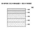
AlNのバッファ層902とGaNのチャネル層905との間にAl組成が高いAl0.86Ga0.14Nのバッファ層を設けることで、チャネル層905に印加される電界を緩和することができる。図3は、量子閉じ込め構造トランジスタを含む第2参考例に係る半導体装置の一部を示す断面図である。 By providing an Al0.86 Ga0.14 N buffer layer having a high Al composition between the
第2参考例に係る半導体装置920では、図3に示すように、AlNのバッファ層902とGaNのチャネル層905との間にAl0.86Ga0.14Nのバッファ層903が設けられている。その他の構成は第1参考例と同様である。図4に、第2参考例に係る半導体装置920のバンド構造を示す。 In the
図4に示すように、第2参考例においては、第1参考例と比較して、チャネル層905に印加される電界が緩和されている。しかしながら、電界が緩和されても、円1で示すように、価電子帯がフェルミ準位Efと重なっており、チャネル層905のバッファ層902との界面近傍に正孔が存在する。As shown in FIG. 4, in the second reference example, the electric field applied to the
Al0.86Ga0.14Nのバッファ層903とGaNのチャネル層905との間にAl組成が低いAl0.30Ga0.70Nのバッファ層を設けることで、チャネル層905に印加される電界を更に緩和することができる。図5は、量子閉じ込め構造トランジスタを含む第3参考例に係る半導体装置の一部を示す断面図である。 By providing anAl0.30Ga0.70N buffer layer having a low Al composition between theAl0.86Ga0.14N
第3参考例に係る半導体装置930では、図5に示すように、Al0.86Ga0.14Nのバッファ層903とGaNのチャネル層905との間にAl0.30Ga0.70Nのバッファ層934が設けられている。ここでは、バッファ層934はバッファ層903に格子整合しておらず、バッファ層934にはバッファ層903からの応力が作用していない。その他の構成は第2参考例と同様である。図6に、第3参考例に係る半導体装置930のバンド構造を示す。 In the
図6に示すように、第3参考例においては、第2参考例と比較して、チャネル層905に印加される電界が緩和されている。しかしながら、チャネル層905を構成するGaNの自発分極によって内部電界が生じ、円1で示すように、正孔が生成される。As shown in FIG. 6, in the third reference example, the electric field applied to the
バッファ層934に代えて、バッファ層903に格子整合し、面内方向においてバッファ層903からの圧縮応力が作用するAl0.30Ga0.70Nのバッファ層が用いられることで、ピエゾ分極によってGaNの自発分極を抑制することができる。図7は、量子閉じ込め構造トランジスタを含む第4参考例に係る半導体装置の一部を示す断面図である。 By using a buffer layer of Al0.30 Ga0.70 N that is lattice-matched to the
第4参考例に係る半導体装置940では、図7に示すように、バッファ層934に代えて、バッファ層903に格子整合し、面内方向においてバッファ層903からの圧縮応力が作用するAl0.30Ga0.70Nのバッファ層904が設けられている。その他の構成は第3参考例と同様である。図8に、第4参考例に係る半導体装置940のバンド構造を示す。 7, in the
図8に示すように、第4参考例によれば、チャネル層905のバッファ層902との界面近傍での正孔の生成を抑制することができる。また、図8中の円2で示すように、チャネル層905のバリア層906との界面近傍において、伝導帯がフェルミ準位Efと重なっている。このため、チャネル層905のバリア層906との界面近傍に電子が生成される。つまり、二次元電子ガス(two-dimensional gas:2DEG)が生成される。As shown in FIG. 8, according to the fourth reference example, the generation of holes near the interface between the
本発明者らは、これらの知見に基づいて、以下のような実施形態に想到した。以下、本開示の実施形態について添付の図面を参照しながら具体的に説明する。なお、本明細書及び図面において、実質的に同一の機能構成を有する構成要素については、同一の符号を付することにより重複した説明を省くことがある。Based on these findings, the inventors have come up with the following embodiment. Hereinafter, the embodiment of the present disclosure will be specifically described with reference to the attached drawings. Note that in this specification and the drawings, components having substantially the same functional configuration may be denoted by the same reference numerals to avoid redundant description.
(第1実施形態)
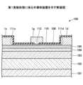
第1実施形態について説明する。第1実施形態は、量子閉じ込め構造の高電子移動度トランジスタ(high electron mobility transistor:HEMT)を含む半導体装置に関する。図9は、第1実施形態に係る半導体装置を示す断面図である。 First Embodiment
A first embodiment will be described. The first embodiment relates to a semiconductor device including a high electron mobility transistor (HEMT) having a quantum confinement structure. Fig. 9 is a cross-sectional view showing the semiconductor device according to the first embodiment.
第1実施形態に係る半導体装置100では、図9に示すように、基板101の上方に窒化物半導体積層構造130が形成されている。窒化物半導体積層構造130には、バッファ層102、バッファ層103、バッファ層104、チャネル層105及びバリア層106が含まれる。バッファ層102は基板101の上に形成されている。バッファ層103はバッファ層102の上に形成されている。バッファ層104はバッファ層103の上に形成されている。チャネル層105はバッファ層104の上に形成されている。バリア層106はチャネル層105の上に形成されている。In the
基板101は、例えばAlN自立基板であり、基板101の上面はAl極性面である。つまり、基板101の上面のミラー指数は(0001)である。バッファ層102は、例えば厚さが50nm~150nmのAlN層である。バッファ層103は、例えば厚さが5nm~20nmのAlx1Ga1-x1N層(0.80≦x1≦0.95)である。バッファ層104は、例えば厚さが25nm~75nmのAlx2Ga1-x2N層(0.20≦x2≦0.40)である。チャネル層105は、例えば厚さが50nm以下のGaN層である。バリア層106は、例えば厚さが4nm~20nmのAlx3Ga1-x3N層(0.50≦x3≦1.00)である。チャネル層105の厚さは好ましくは50nm以下であり、より好ましくは20nm以下である。優れた量子閉じ込め効果を得るためである。例えば、バッファ層103はバッファ層102に格子整合し、バッファ層104はバッファ層103に格子整合し、チャネル層105はバッファ層104に格子整合する。バリア層106がチャネル層105に格子整合してもよい。バッファ層102~104、チャネル層105及びバリア層106の上面のミラー指数も(0001)である。 The
バッファ層103には、基板101及びバッファ層102の厚さ方向に垂直な面内方向でバッファ層102から圧縮応力が印加される。バッファ層104には、上記面内方向でバッファ層103から圧縮応力が印加される。チャネル層105には、上記面内方向でバッファ層104から圧縮応力が印加される。バリア層106には、上記面内方向でチャネル層105から引張応力が印加されてもよい。A compressive stress is applied from the
バッファ層102は下地の一例であり、バッファ層102のAlNは第1窒化物半導体の一例である。下地に基板101が含まれてもよい。バッファ層103は第1バッファ層の一例であり、バッファ層103のAlx1Ga1-x1N(0.80≦x1≦0.95)は第2窒化物半導体の一例である。バッファ層104は第2バッファ層の一例であり、バッファ層104のAlx2Ga1-x2N(0.20≦x2≦0.40)は第3窒化物半導体の一例である。チャネル層105のGaNは第4窒化物半導体の一例である。バリア層106のAlx3Ga1-x3N(0.50≦x3≦1.00)は第5窒化物半導体の一例である。 The
窒化物半導体積層構造130に、素子領域を画定する素子分離領域が形成されており、素子領域内において、バリア層106にソース用の開口部111s及びドレイン用の開口部111dが形成されている。開口部111sにソース電極1sが形成され、開口部111dにドレイン電極1dが形成されている。ソース電極1s及びドレイン電極1dは窒化物半導体積層構造130にオーミック接触している。バリア層106の上に、ソース電極1s及びドレイン電極1dを覆うパッシベーション膜110が形成されている。パッシベーション膜110には、平面視でソース電極1s及びドレイン電極1dの間に位置する開口部112が形成されており、開口部112を通じてバリア層106と接するゲート電極1gがパッシベーション膜110の上に形成されている。An element isolation region that defines an element region is formed in the nitride semiconductor laminate structure 130, and an
ソース電極1s及びドレイン電極1dは、例えば厚さが10nm~50nmのTa膜及びその上の厚さが100nm~500nmのAl膜を含む。ゲート電極1gは、例えば厚さが10nm~50nmのNi膜及びその上の厚さが300nm~500nmのAu膜を含み、窒化物半導体積層構造130とショットキー接触している。パッシベーション膜110は、例えばSi、Al、Hf、Zr、Ti、Ta又はWの酸化物、窒化物又は酸窒化物の膜であり、好ましくはSi窒化物(SiN)の膜である。パッシベーション膜110の厚さは、例えば2nm~500nmであり、好ましくは100nm程度である。The
第1実施形態に係る半導体装置100においては、バッファ層102、バッファ層103、バッファ層104、チャネル層105及びバリア層106が、第4参考例におけるバッファ層902、バッファ層903、バッファ層904、チャネル層905及びバリア層906と同様のバンド構造(図8参照)を有する。従って、高濃度の二次元電子ガス(2DEG)がチャネル層105のバリア層106との界面近傍に存在し、チャネル層105のバッファ層104との界面近傍には正孔が存在しない。このため、シート抵抗及びリーク電流を低減することができる。In the
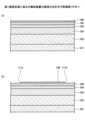
次に、第1実施形態に係る半導体装置100の製造方法について説明する。図10~図11は、第1実施形態に係る半導体装置100の製造方法を示す断面図である。Next, a method for manufacturing the
まず、図10(a)に示すように、基板101の(0001)面上に窒化物半導体積層構造130を形成する。窒化物半導体積層構造130の形成では、バッファ層102、バッファ層103、バッファ層104、チャネル層105及びバリア層106を、例えば有機金属気相成長(MOVPE:metal organic vapor phase epitaxy)法により形成する。窒化物半導体積層構造130の形成に際して、原料ガスとして、例えば、Al源であるトリメチルアルミニウム(TMAl)ガスと、Ga源であるトリメチルガリウム(TMGa)ガスと、N源であるアンモニア(NH3)ガスとの混合ガスを用いる。キャリアガスとして水素(H2)ガス又は窒素(N2)ガスを用いる。成長させる窒化物半導体層の組成に応じて、TMAlガス及びTMGaガスの供給の有無及び流量を適宜設定する。例えば、成長圧力は1kPa~100kPa程度、成長温度は700℃~1500℃程度とする。窒化物半導体層にInが含まれる場合、In源としてトリメチルインジウム(In)を用いることができる。特に、バッファ層103をバッファ層102と格子整合させるために、バッファ層103の成長温度は、700℃~950℃とすることが好ましい。また、バッファ層104をバッファ層103と格子整合させるために、バッファ層104の成長温度は、700℃~950℃とすることが好ましい。 First, as shown in FIG. 10A, a nitride semiconductor laminate structure 130 is formed on the (0001) surface of a
次いで、窒化物半導体積層構造130に、素子領域を画定する素子分離領域を形成する。素子分離領域の形成では、例えば、素子分離領域を形成する予定の領域を露出するフォトレジストのパターンを窒化物半導体積層構造130上に形成し、このパターンをマスクとしてAr等のイオン注入を行う。このパターンをエッチングマスクとして塩素系ガスを用いたドライエッチングを行ってもよい。Next, an isolation region that defines an element region is formed in the nitride semiconductor laminate structure 130. In forming the isolation region, for example, a photoresist pattern that exposes the region where the isolation region is to be formed is formed on the nitride semiconductor laminate structure 130, and ions such as Ar are implanted using this pattern as a mask. Dry etching using a chlorine-based gas may be performed using this pattern as an etching mask.
その後、図10(b)に示すように、バリア層106にソース用の開口部111s及びドレイン用の開口部111dを形成する。開口部111s及び111dの形成では、例えば、フォトリソグラフィにより開口部111s及び111dを形成する予定の領域を露出するフォトレジストのパターンをバリア層106の上に形成し、このパターンをエッチングマスクとして弗素系ガス又は塩素系ガスを用いたドライエッチングを行う。この結果、チャネル層105が開口部111s及び111dに露出する。After that, as shown in FIG. 10(b), an
続いて、図11(a)に示すように、開口部111s内にソース電極1sを形成し、開口部111d内にドレイン電極1dを形成する。ソース電極1s及びドレイン電極1dは、例えばリフトオフ法により形成することができる。すなわち、ソース電極1s及びドレイン電極1dを形成する予定の領域を露出するフォトレジストのパターンを形成し、このパターンを成長マスクとして蒸着法により金属膜を形成し、このパターンをその上の金属膜と共に除去する。金属膜の形成では、例えば、Ta膜を形成し、その上にAl膜を形成する。次いで、例えば、窒素雰囲気中にて400℃~1000℃、好ましくは550℃程度で熱処理を行い、オーミック特性を確立する。Next, as shown in FIG. 11(a), a
続いて、図11(b)に示すように、バリア層106の上にソース電極1s及びドレイン電極1dを覆うパッシベーション膜110を形成する。パッシベーション膜110は、例えばプラズマCVD法により形成することができる。パッシベーション膜110は、ALD法又はスパッタ法により形成してもよい。次いで、パッシベーション膜110に開口部112を形成する。開口部112の形成では、例えば、フォトリソグラフィにより開口部112を形成する予定の領域を露出するフォトレジストのパターンをパッシベーション膜110の上に形成し、このパターンをエッチングマスクとして弗素系ガス又は塩素系ガスを用いたドライエッチングを行う。ドライエッチングに代えて、弗酸又はバッファード弗酸等を用いたウェットエッチングを行ってもよい。Next, as shown in FIG. 11(b), a
その後、開口部112を通じてバリア層106に接するゲート電極1gをパッシベーション膜110上に形成する(図9参照)。ゲート電極1gは、例えばリフトオフ法により形成することができる。すなわち、ゲート電極1gを形成する予定の領域を露出するフォトレジストのパターンを形成し、このパターンを成長マスクとして蒸着法により金属膜を形成し、このパターンをその上の金属膜と共に除去する。金属膜の形成では、例えば、Ni膜を形成し、その上にAu膜を形成する。Then, a
このようにして、第1実施形態に係る半導体装置100を製造することができる。In this manner, the
バッファ層102(下地)がAlN層であり、チャネル層105がGaN層である場合、AlGaNのバッファ層103のAl組成x1は0.80以上0.95以下であり、AlGaNのバッファ層104のAl組成x2は0.20以上0.40以下であることが好ましい。Al組成x1が0.80未満であると、バッファ層103をバッファ層102に格子整合させにくいことがある。Al組成x1が0.95超であると、バッファ層104をバッファ層103に格子整合させにくいことがある。また、Al組成x2が0.20未満であると、バッファ層104をバッファ層103に格子整合させにくいことがある。Al組成x2が0.40超であると、チャネル層105をバッファ層104に格子整合させにくいことがある。なお、バッファ層103及び104の材料はAlGaNに限定されず、応力の関係が適切であれば、InAlGaNがバッファ層103及び104に用いられてもよい。When the buffer layer 102 (underlying) is an AlN layer and the
(第2実施形態)
次に、第2実施形態について説明する。第2実施形態は、HEMTのディスクリートパッケージに関する。図12は、第2実施形態に係るディスクリートパッケージを示す図である。 Second Embodiment
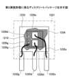
Next, a second embodiment will be described. The second embodiment relates to a discrete package of a HEMT. Fig. 12 is a diagram showing the discrete package according to the second embodiment.
第2実施形態では、図12に示すように、第1実施形態と同様の構造を備えた半導体装置1210の裏面がはんだ等のダイアタッチ剤1234を用いてランド(ダイパッド)1233に固定されている。また、ドレイン電極1dが接続されたドレインパッド1226dに、Alワイヤ等のワイヤ1235dが接続され、ワイヤ1235dの他端が、ランド1233と一体化しているドレインリード1232dに接続されている。ソース電極1sに接続されたソースパッド1226sにAlワイヤ等のワイヤ1235sが接続され、ワイヤ1235sの他端がランド1233から独立したソースリード1232sに接続されている。ゲート電極1gに接続されたゲートパッド1226gにAlワイヤ等のワイヤ1235gが接続され、ワイヤ1235gの他端がランド1233から独立したゲートリード1232gに接続されている。そして、ゲートリード1232gの一部、ドレインリード1232dの一部及びソースリード1232sの一部が突出するようにして、ランド1233及び半導体装置1210等がモールド樹脂1231によりパッケージングされている。In the second embodiment, as shown in FIG. 12, the back surface of a
このようなディスクリートパッケージは、例えば、次のようにして製造することができる。まず、半導体装置1210をはんだ等のダイアタッチ剤1234を用いてリードフレームのランド1233に固定する。次いで、ワイヤ1235g、1235d及び1235sを用いたボンディングにより、ゲートパッド1226gをリードフレームのゲートリード1232gに接続し、ドレインパッド1226dをリードフレームのドレインリード1232dに接続し、ソースパッド1226sをリードフレームのソースリード1232sに接続する。その後、トランスファーモールド法にてモールド樹脂1231を用いた封止を行う。続いて、リードフレームを切り離す。Such a discrete package can be manufactured, for example, as follows. First, the
(第3実施形態)
次に、第3実施形態について説明する。第3実施形態は、HEMTを備えたPFC(Power Factor Correction)回路に関する。図13は、第3実施形態に係るPFC回路を示す結線図である。 Third Embodiment
Next, a third embodiment will be described. The third embodiment relates to a PFC (Power Factor Correction) circuit including a HEMT. Fig. 13 is a wiring diagram showing the PFC circuit according to the third embodiment.
PFC回路1250には、スイッチ素子(トランジスタ)1251、ダイオード1252、チョークコイル1253、コンデンサ1254及び1255、ダイオードブリッジ1256、並びに交流電源(AC)1257が設けられている。そして、スイッチ素子1251のドレイン電極と、ダイオード1252のアノード端子及びチョークコイル1253の一端子とが接続されている。スイッチ素子1251のソース電極と、コンデンサ1254の一端子及びコンデンサ1255の一端子とが接続されている。コンデンサ1254の他端子とチョークコイル1253の他端子とが接続されている。コンデンサ1255の他端子とダイオード1252のカソード端子とが接続されている。また、スイッチ素子1251のゲート電極にはゲートドライバが接続されている。コンデンサ1254の両端子間には、ダイオードブリッジ1256を介してAC1257が接続される。コンデンサ1255の両端子間には、直流電源(DC)が接続される。そして、本実施形態では、スイッチ素子1251に、第1実施形態と同様の構造を備えた半導体装置が用いられている。The
PFC回路1250の製造に際しては、例えば、はんだ等を用いて、スイッチ素子1251をダイオード1252及びチョークコイル1253等に接続する。When manufacturing the
(第4実施形態)
次に、第4実施形態について説明する。第4実施形態は、サーバ電源に好適な、HEMTを備えた電源装置に関する。図14は、第4実施形態に係る電源装置を示す結線図である。 Fourth Embodiment
Next, a fourth embodiment will be described. The fourth embodiment relates to a power supply device equipped with a HEMT, suitable for use as a server power supply. Fig. 14 is a wiring diagram showing the power supply device according to the fourth embodiment.
電源装置には、高圧の一次側回路1261及び低圧の二次側回路1262、並びに一次側回路1261と二次側回路1262との間に配設されるトランス1263が設けられている。The power supply device is provided with a high-voltage
一次側回路1261には、第3実施形態に係るPFC回路1250、及びPFC回路1250のコンデンサ1255の両端子間に接続されたインバータ回路、例えばフルブリッジインバータ回路1260が設けられている。フルブリッジインバータ回路1260には、複数(ここでは4つ)のスイッチ素子1264a、1264b、1264c及び1264dが設けられている。The
二次側回路1262には、複数(ここでは3つ)のスイッチ素子1265a、1265b及び1265cが設けられている。The
本実施形態では、一次側回路1261を構成するPFC回路1250のスイッチ素子1251、並びにフルブリッジインバータ回路1260のスイッチ素子1264a、1264b、1264c及び1264dに、第1実施形態と同様の構造を備えた半導体装置が用いられている。一方、二次側回路1262のスイッチ素子1265a、1265b及び1265cには、シリコンを用いた通常のMIS型FET(電界効果トランジスタ)が用いられている。In this embodiment, the
(第5実施形態)
次に、第5実施形態について説明する。第5実施形態は、HEMTを備えた増幅器に関する。図15は、第5実施形態に係る増幅器を示す結線図である。 Fifth Embodiment
Next, a fifth embodiment will be described. The fifth embodiment relates to an amplifier including a HEMT. Fig. 15 is a wiring diagram showing the amplifier according to the fifth embodiment.
増幅器には、ディジタル・プレディストーション回路1271、ミキサー1272a及び1272b、並びにパワーアンプ1273が設けられている。The amplifier includes a
ディジタル・プレディストーション回路1271は、入力信号の非線形歪みを補償する。ミキサー1272aは、非線形歪みが補償された入力信号と交流信号とをミキシングする。パワーアンプ1273は、第1実施形態と同様の構造を備えた半導体装置を備えており、交流信号とミキシングされた入力信号を増幅する。なお、本実施形態では、例えば、スイッチの切り替えにより、出力側の信号をミキサー1272bで交流信号とミキシングしてディジタル・プレディストーション回路1271に送出できる。この増幅器は、高周波増幅器、高出力増幅器として使用することができる。高周波増幅器は、例えば、携帯電話基地局用送受信装置、レーダー装置及びマイクロ波発生装置に用いることができる。The
本開示において、基板として、炭化シリコン(SiC)基板、サファイヤ基板、シリコン基板、AlN基板、GaN基板又はダイヤモンド基板を用いてもよい。基板が、導電性、半絶縁性又は絶縁性のいずれであってもよい。電子走行層を基板上に形成できる場合、基板が下地として用いられてもよい。In the present disclosure, the substrate may be a silicon carbide (SiC) substrate, a sapphire substrate, a silicon substrate, an AlN substrate, a GaN substrate, or a diamond substrate. The substrate may be conductive, semi-insulating, or insulating. If an electron transport layer can be formed on the substrate, the substrate may be used as a base.
ゲート電極、ソース電極及びドレイン電極の構造は上述の実施形態のものに限定されない。例えば、これらが単層から構成されていてもよい。また、これらの形成方法はリフトオフ法に限定されない。更に、オーミック特性が得られるのであれば、ソース電極及びドレイン電極の形成後の熱処理を省略してもよい。ゲート電極の形成後に熱処理を行ってもよい。The structures of the gate electrode, source electrode, and drain electrode are not limited to those in the above-described embodiment. For example, they may be composed of a single layer. Furthermore, the method of forming them is not limited to the lift-off method. Furthermore, if ohmic characteristics are obtained, the heat treatment after the formation of the source electrode and drain electrode may be omitted. Heat treatment may be performed after the formation of the gate electrode.
ゲート電極の構造として、上記の実施形態ではショットキー型ゲート構造が用いられているが、MIS(metal-insulator-semiconductor)型ゲート構造が用いられてもよい。In the above embodiment, a Schottky gate structure is used as the gate electrode structure, but a MIS (metal-insulator-semiconductor) gate structure may also be used.
以上、好ましい実施の形態等について詳説したが、上述した実施の形態等に制限されることはなく、特許請求の範囲に記載された範囲を逸脱することなく、上述した実施の形態等に種々の変形及び置換を加えることができる。Although the preferred embodiments have been described above in detail, the present invention is not limited to the above-described embodiments, and various modifications and substitutions can be made to the above-described embodiments without departing from the scope of the claims.
以下、本開示の諸態様を付記としてまとめて記載する。Various aspects of this disclosure are summarized below as appendices.
(付記1)
第1窒化物半導体の下地と、
前記下地の上に設けられ、前記下地の厚さ方向に垂直な面内方向で前記下地から圧縮応力を受ける第2窒化物半導体の第1バッファ層と、
前記第1バッファ層の上に設けられ、面内方向で前記第1バッファ層から圧縮応力を受ける第3窒化物半導体の第2バッファ層と、
前記第2バッファ層の上に設けられ、面内方向で前記第2バッファ層から圧縮応力を受ける第4窒化物半導体のチャネル層と、
前記チャネル層の上方に設けられた第5窒化物半導体のバリア層と、
を有することを特徴とする半導体装置。
(付記2)
前記第2窒化物半導体は、Al及びGaを含み、
前記第3窒化物半導体は、Al及びGaを含み、
前記第2窒化物半導体のAl組成は、前記第3窒化物半導体のAl組成よりも高いことを特徴とする付記1に記載の半導体装置。
(付記3)
前記第1バッファ層は、前記下地に格子整合し、
前記第2バッファ層は、前記第1バッファ層に格子整合し、
前記チャネル層は、前記第2バッファ層に格子整合することを特徴とする付記1又は2に記載の半導体装置。
(付記4)
前記バリア層は、前記チャネル層に格子整合することを特徴とする付記3に記載の半導体装置。
(付記5)
前記チャネル層の厚さが50nm以下であることを特徴とする付記1乃至4のいずれか1項に記載の半導体装置。
(付記6)
前記第1窒化物半導体は、AlNであることを特徴とする付記1乃至5のいずれか1項に記載の半導体装置。
(付記7)
前記下地の表面が(0001)面であることを特徴とする付記6に記載の半導体装置。
(付記8)
前記第2窒化物半導体の組成は、Alx1Ga1-x1N(0.80≦x1≦0.95)で表され
前記第3窒化物半導体の組成は、Alx2Ga1-x2N(0.20≦x2≦0.40)で表され
前記第4窒化物半導体は、GaNであることを特徴とする付記6又は7に記載の半導体装置。
(付記9)
付記1乃至8のいずれか1項に記載の半導体装置を有することを特徴とする増幅器。
(付記10)
付記1乃至8のいずれか1項に記載の半導体装置を有することを特徴とする電源装置。 (Appendix 1)
A first nitride semiconductor underlayer;
a first buffer layer made of a second nitride semiconductor provided on the underlayer and receiving a compressive stress from the underlayer in an in-plane direction perpendicular to a thickness direction of the underlayer;
a second buffer layer made of a third nitride semiconductor provided on the first buffer layer and receiving a compressive stress from the first buffer layer in an in-plane direction;
a fourth nitride semiconductor channel layer provided on the second buffer layer and receiving a compressive stress from the second buffer layer in an in-plane direction;
a barrier layer made of a fifth nitride semiconductor provided above the channel layer;
A semiconductor device comprising:
(Appendix 2)
the second nitride semiconductor contains Al and Ga;
the third nitride semiconductor contains Al and Ga;
2. The semiconductor device according to
(Appendix 3)
the first buffer layer is lattice-matched to the underlayer;
the second buffer layer is lattice-matched to the first buffer layer;
3. The semiconductor device according to
(Appendix 4)
4. The semiconductor device according to
(Appendix 5)
5. The semiconductor device according to
(Appendix 6)
6. The semiconductor device according to
(Appendix 7)
7. The semiconductor device according to claim 6, wherein the surface of the base is a (0001) plane.
(Appendix 8)
The semiconductor device according to
(Appendix 9)
9. An amplifier comprising the semiconductor device according to any one of
(Appendix 10)
A power supply device comprising the semiconductor device according to any one of
1s:ソース電極
1d:ドレイン電極
1g:ゲート電極
100:半導体装置
101:基板
102、103、104:バッファ層
105:チャネル層
106:バリア層 1s:
Claims (4)
Translated fromJapanese前記下地の上に設けられ、前記下地の厚さ方向に垂直な面内方向で前記下地から圧縮応力を受ける第2窒化物半導体の第1バッファ層と、
前記第1バッファ層の上に設けられ、前記面内方向で前記第1バッファ層から圧縮応力を受ける第3窒化物半導体の第2バッファ層と、
前記第2バッファ層の上に設けられ、前記面内方向で前記第2バッファ層から圧縮応力を受ける第4窒化物半導体のチャネル層と、
前記チャネル層の上方に設けられた第5窒化物半導体のバリア層と、
を有し、
前記第2窒化物半導体の組成はAlx1Ga1-x1N(0.80≦x1≦0.95)で表され、
前記第3窒化物半導体の組成はAlx2Ga1-x2N(0.20≦x2≦0.40)で表されることを特徴とする半導体装置。 A first nitride semiconductor underlayer;
a first buffer layer made of a second nitride semiconductor provided on the underlayer and receiving a compressive stress from the underlayer in an in-plane direction perpendicular to a thickness direction of the underlayer;
a second buffer layer made of a third nitride semiconductor provided on the first buffer layer and receiving a compressive stress from the first buffer layer in the in-plane direction;
a fourth nitride semiconductor channel layer provided on the second buffer layer and receiving a compressive stress from the second buffer layer in the in-plane direction;
a barrier layer made of a fifth nitride semiconductor provided above the channel layer;
having
The composition of the second nitride semiconductoris expressed by Alx1Ga1-x1 N (0.80≦x1≦0.95),
A semiconductor device, whereinthe composition of the third nitride semiconductor is expressed as Alx2Ga1-x2N (0.20≦x2≦0.40) .
前記第2バッファ層は、前記第1バッファ層に格子整合し、
前記チャネル層は、前記第2バッファ層に格子整合することを特徴とする請求項1に記載の半導体装置。 the first buffer layer is lattice-matched to the underlayer;
the second buffer layer is lattice-matched to the first buffer layer;
2. The semiconductor device accordingto claim 1 , wherein the channel layer is lattice-matched to the second buffer layer.
Priority Applications (2)
| Application Number | Priority Date | Filing Date | Title |
|---|---|---|---|
| JP2020119964AJP7613012B2 (en) | 2020-07-13 | 2020-07-13 | Semiconductor Device |
| US17/209,869US11791384B2 (en) | 2020-07-13 | 2021-03-23 | Semiconductor device |
Applications Claiming Priority (1)
| Application Number | Priority Date | Filing Date | Title |
|---|---|---|---|
| JP2020119964AJP7613012B2 (en) | 2020-07-13 | 2020-07-13 | Semiconductor Device |
Publications (2)
| Publication Number | Publication Date |
|---|---|
| JP2022016951A JP2022016951A (en) | 2022-01-25 |
| JP7613012B2true JP7613012B2 (en) | 2025-01-15 |
Family
ID=79173845
Family Applications (1)
| Application Number | Title | Priority Date | Filing Date |
|---|---|---|---|
| JP2020119964AActiveJP7613012B2 (en) | 2020-07-13 | 2020-07-13 | Semiconductor Device |
Country Status (2)
| Country | Link |
|---|---|
| US (1) | US11791384B2 (en) |
| JP (1) | JP7613012B2 (en) |
Citations (10)
| Publication number | Priority date | Publication date | Assignee | Title |
|---|---|---|---|---|
| JP2008539587A (en) | 2005-04-29 | 2008-11-13 | クリー インコーポレイテッド | High electron mobility transistor based on binary group III nitride and method of manufacturing the same |
| JP2011003652A (en) | 2009-06-17 | 2011-01-06 | Fujitsu Ltd | Semiconductor device, and method for manufacturing the same |
| WO2011155496A1 (en) | 2010-06-08 | 2011-12-15 | 日本碍子株式会社 | Epitaxial substrate and method for producing epitaxial substrate |
| JP2012243871A (en) | 2011-05-17 | 2012-12-10 | Advanced Power Device Research Association | Semiconductor device and method of manufacturing the same |
| JP2013042032A (en) | 2011-08-18 | 2013-02-28 | Fujitsu Ltd | Compound semiconductor device and manufacturing method thereof |
| JP2013145782A (en) | 2012-01-13 | 2013-07-25 | Sharp Corp | Epitaxial wafer for hetero-junction field effect transistor |
| JP2013187428A (en) | 2012-03-08 | 2013-09-19 | Toshiba Corp | Method of manufacturing nitride semiconductor layer |
| JP2015060986A (en) | 2013-09-19 | 2015-03-30 | 富士通株式会社 | Semiconductor device and semiconductor device manufacturing method |
| JP2015512148A (en) | 2012-02-03 | 2015-04-23 | トランスフォーム インコーポレーテッド | Buffer layer structure suitable for III-nitride devices with dissimilar substrates |
| JP2019033122A (en) | 2017-08-04 | 2019-02-28 | 富士通株式会社 | Compound semiconductor device, compound semiconductor device manufacturing method, power supply device, and high-frequency amplifier |
Family Cites Families (5)
| Publication number | Priority date | Publication date | Assignee | Title |
|---|---|---|---|---|
| EP1978550A4 (en) | 2005-12-28 | 2009-07-22 | Nec Corp | FIELD EFFECT TRANSISTOR, AND MULTILAYER EPITAXIAL FILM FOR USE IN FIELD EFFECT TRANSISTOR PREPARATION |
| US9233844B2 (en)* | 2012-06-27 | 2016-01-12 | Taiwan Semiconductor Manufacturing Co., Ltd. | Graded aluminum—gallium—nitride and superlattice buffer layer for III-V nitride layer on silicon substrate |
| JP6119165B2 (en)* | 2012-09-28 | 2017-04-26 | 富士通株式会社 | Semiconductor device |
| JP5462377B1 (en)* | 2013-01-04 | 2014-04-02 | Dowaエレクトロニクス株式会社 | Group III nitride epitaxial substrate and manufacturing method thereof |
| JP2014220407A (en)* | 2013-05-09 | 2014-11-20 | ローム株式会社 | Nitride semiconductor element |
- 2020
- 2020-07-13JPJP2020119964Apatent/JP7613012B2/enactiveActive
- 2021
- 2021-03-23USUS17/209,869patent/US11791384B2/enactiveActive
Patent Citations (10)
| Publication number | Priority date | Publication date | Assignee | Title |
|---|---|---|---|---|
| JP2008539587A (en) | 2005-04-29 | 2008-11-13 | クリー インコーポレイテッド | High electron mobility transistor based on binary group III nitride and method of manufacturing the same |
| JP2011003652A (en) | 2009-06-17 | 2011-01-06 | Fujitsu Ltd | Semiconductor device, and method for manufacturing the same |
| WO2011155496A1 (en) | 2010-06-08 | 2011-12-15 | 日本碍子株式会社 | Epitaxial substrate and method for producing epitaxial substrate |
| JP2012243871A (en) | 2011-05-17 | 2012-12-10 | Advanced Power Device Research Association | Semiconductor device and method of manufacturing the same |
| JP2013042032A (en) | 2011-08-18 | 2013-02-28 | Fujitsu Ltd | Compound semiconductor device and manufacturing method thereof |
| JP2013145782A (en) | 2012-01-13 | 2013-07-25 | Sharp Corp | Epitaxial wafer for hetero-junction field effect transistor |
| JP2015512148A (en) | 2012-02-03 | 2015-04-23 | トランスフォーム インコーポレーテッド | Buffer layer structure suitable for III-nitride devices with dissimilar substrates |
| JP2013187428A (en) | 2012-03-08 | 2013-09-19 | Toshiba Corp | Method of manufacturing nitride semiconductor layer |
| JP2015060986A (en) | 2013-09-19 | 2015-03-30 | 富士通株式会社 | Semiconductor device and semiconductor device manufacturing method |
| JP2019033122A (en) | 2017-08-04 | 2019-02-28 | 富士通株式会社 | Compound semiconductor device, compound semiconductor device manufacturing method, power supply device, and high-frequency amplifier |
Also Published As
| Publication number | Publication date |
|---|---|
| US20220013642A1 (en) | 2022-01-13 |
| JP2022016951A (en) | 2022-01-25 |
| US11791384B2 (en) | 2023-10-17 |
Similar Documents
| Publication | Publication Date | Title |
|---|---|---|
| KR101458292B1 (en) | Compound semiconductor device and method of manufacturing the same | |
| US9653569B1 (en) | Compound semiconductor device and manufacturing method thereof | |
| US10707338B2 (en) | Semiconductor device and method of manufacturing the same | |
| US10964805B2 (en) | Compound semiconductor device | |
| JP6703269B2 (en) | Compound semiconductor device and manufacturing method thereof | |
| US10665710B2 (en) | Compound semiconductor device and fabrication method | |
| US20180145148A1 (en) | Compound semiconductor device | |
| US20130256754A1 (en) | Compound semiconductor device and method for manufacturing the same | |
| JP2020072218A (en) | Compound semiconductor device, high frequency amplifier and power supply device | |
| JP2023080485A (en) | Semiconductor device | |
| JP7543773B2 (en) | Semiconductor device and its manufacturing method | |
| JP7545044B2 (en) | Semiconductor device, manufacturing method thereof, and electronic device | |
| JP7439536B2 (en) | semiconductor equipment | |
| JP7528583B2 (en) | Semiconductor Device | |
| US11824108B2 (en) | Semiconductor device | |
| JP7613012B2 (en) | Semiconductor Device | |
| JP7484785B2 (en) | NITRIDE SEMICONDUCTOR DEVICE AND METHOD FOR MANUFACTURING NITRIDE SEMICONDUCTOR DEVICE - Patent application | |
| JP2022016950A (en) | Semiconductor device | |
| JP6631057B2 (en) | Compound semiconductor device and method of manufacturing the same | |
| JP7620203B2 (en) | Semiconductor device, manufacturing method thereof, and electronic device | |
| JP6187167B2 (en) | Compound semiconductor device and manufacturing method thereof | |
| US20250311276A1 (en) | Semiconductor device | |
| JP2019050233A (en) | Semiconductor device and method for manufacturing the same | |
| JP2025002282A (en) | NITRIDE SEMICONDUCTOR DEVICE, METHOD FOR MANUFACTURING NITRIDE SEMICONDUCTOR DEVICE, AND EPITAXIAL SUBSTRATE | |
| JP2024114336A (en) | NITRIDE SEMICONDUCTOR DEVICE AND METHOD FOR MANUFACTURING NITRIDE SEMICON |
Legal Events
| Date | Code | Title | Description |
|---|---|---|---|
| A621 | Written request for application examination | Free format text:JAPANESE INTERMEDIATE CODE: A621 Effective date:20230407 | |
| A977 | Report on retrieval | Free format text:JAPANESE INTERMEDIATE CODE: A971007 Effective date:20240110 | |
| A131 | Notification of reasons for refusal | Free format text:JAPANESE INTERMEDIATE CODE: A131 Effective date:20240123 | |
| A131 | Notification of reasons for refusal | Free format text:JAPANESE INTERMEDIATE CODE: A131 Effective date:20240702 | |
| A521 | Request for written amendment filed | Free format text:JAPANESE INTERMEDIATE CODE: A523 Effective date:20240819 | |
| TRDD | Decision of grant or rejection written | ||
| A01 | Written decision to grant a patent or to grant a registration (utility model) | Free format text:JAPANESE INTERMEDIATE CODE: A01 Effective date:20241126 | |
| A61 | First payment of annual fees (during grant procedure) | Free format text:JAPANESE INTERMEDIATE CODE: A61 Effective date:20241209 | |
| R150 | Certificate of patent or registration of utility model | Ref document number:7613012 Country of ref document:JP Free format text:JAPANESE INTERMEDIATE CODE: R150 |