JP7611837B2 - Polysilicon Liner - Google Patents
Polysilicon LinerDownload PDFInfo
- Publication number
- JP7611837B2 JP7611837B2JP2021547411AJP2021547411AJP7611837B2JP 7611837 B2JP7611837 B2JP 7611837B2JP 2021547411 AJP2021547411 AJP 2021547411AJP 2021547411 AJP2021547411 AJP 2021547411AJP 7611837 B2JP7611837 B2JP 7611837B2
- Authority
- JP
- Japan
- Prior art keywords
- polysilicon liner
- underlayer
- amorphous silicon
- percent
- depositing
- Prior art date
- Legal status (The legal status is an assumption and is not a legal conclusion. Google has not performed a legal analysis and makes no representation as to the accuracy of the status listed.)
- Active
Links
Images


Classifications
- H—ELECTRICITY
- H01—ELECTRIC ELEMENTS
- H01L—SEMICONDUCTOR DEVICES NOT COVERED BY CLASS H10
- H01L21/00—Processes or apparatus adapted for the manufacture or treatment of semiconductor or solid state devices or of parts thereof
- H01L21/02—Manufacture or treatment of semiconductor devices or of parts thereof
- H01L21/02104—Forming layers
- H01L21/02365—Forming inorganic semiconducting materials on a substrate
- H01L21/02436—Intermediate layers between substrates and deposited layers
- H01L21/02439—Materials
- H01L21/02488—Insulating materials
- H—ELECTRICITY
- H01—ELECTRIC ELEMENTS
- H01L—SEMICONDUCTOR DEVICES NOT COVERED BY CLASS H10
- H01L21/00—Processes or apparatus adapted for the manufacture or treatment of semiconductor or solid state devices or of parts thereof
- H01L21/02—Manufacture or treatment of semiconductor devices or of parts thereof
- H01L21/02104—Forming layers
- H01L21/02365—Forming inorganic semiconducting materials on a substrate
- H01L21/02436—Intermediate layers between substrates and deposited layers
- H01L21/02439—Materials
- H01L21/02441—Group 14 semiconducting materials
- H01L21/0245—Silicon, silicon germanium, germanium
- H—ELECTRICITY
- H01—ELECTRIC ELEMENTS
- H01L—SEMICONDUCTOR DEVICES NOT COVERED BY CLASS H10
- H01L21/00—Processes or apparatus adapted for the manufacture or treatment of semiconductor or solid state devices or of parts thereof
- H01L21/02—Manufacture or treatment of semiconductor devices or of parts thereof
- H01L21/02104—Forming layers
- H01L21/02107—Forming insulating materials on a substrate
- H01L21/02109—Forming insulating materials on a substrate characterised by the type of layer, e.g. type of material, porous/non-porous, pre-cursors, mixtures or laminates
- H01L21/02112—Forming insulating materials on a substrate characterised by the type of layer, e.g. type of material, porous/non-porous, pre-cursors, mixtures or laminates characterised by the material of the layer
- H01L21/02123—Forming insulating materials on a substrate characterised by the type of layer, e.g. type of material, porous/non-porous, pre-cursors, mixtures or laminates characterised by the material of the layer the material containing silicon
- H01L21/02164—Forming insulating materials on a substrate characterised by the type of layer, e.g. type of material, porous/non-porous, pre-cursors, mixtures or laminates characterised by the material of the layer the material containing silicon the material being a silicon oxide, e.g. SiO2
- H—ELECTRICITY
- H01—ELECTRIC ELEMENTS
- H01L—SEMICONDUCTOR DEVICES NOT COVERED BY CLASS H10
- H01L21/00—Processes or apparatus adapted for the manufacture or treatment of semiconductor or solid state devices or of parts thereof
- H01L21/02—Manufacture or treatment of semiconductor devices or of parts thereof
- H01L21/02104—Forming layers
- H01L21/02365—Forming inorganic semiconducting materials on a substrate
- H01L21/02436—Intermediate layers between substrates and deposited layers
- H01L21/02494—Structure
- H01L21/02496—Layer structure
- H01L21/02502—Layer structure consisting of two layers
- H—ELECTRICITY
- H01—ELECTRIC ELEMENTS
- H01L—SEMICONDUCTOR DEVICES NOT COVERED BY CLASS H10
- H01L21/00—Processes or apparatus adapted for the manufacture or treatment of semiconductor or solid state devices or of parts thereof
- H01L21/02—Manufacture or treatment of semiconductor devices or of parts thereof
- H01L21/02104—Forming layers
- H01L21/02365—Forming inorganic semiconducting materials on a substrate
- H01L21/02436—Intermediate layers between substrates and deposited layers
- H01L21/02494—Structure
- H01L21/02513—Microstructure
- H—ELECTRICITY
- H01—ELECTRIC ELEMENTS
- H01L—SEMICONDUCTOR DEVICES NOT COVERED BY CLASS H10
- H01L21/00—Processes or apparatus adapted for the manufacture or treatment of semiconductor or solid state devices or of parts thereof
- H01L21/02—Manufacture or treatment of semiconductor devices or of parts thereof
- H01L21/02104—Forming layers
- H01L21/02365—Forming inorganic semiconducting materials on a substrate
- H01L21/02518—Deposited layers
- H01L21/02521—Materials
- H01L21/02524—Group 14 semiconducting materials
- H01L21/02532—Silicon, silicon germanium, germanium
- H—ELECTRICITY
- H01—ELECTRIC ELEMENTS
- H01L—SEMICONDUCTOR DEVICES NOT COVERED BY CLASS H10
- H01L21/00—Processes or apparatus adapted for the manufacture or treatment of semiconductor or solid state devices or of parts thereof
- H01L21/02—Manufacture or treatment of semiconductor devices or of parts thereof
- H01L21/02104—Forming layers
- H01L21/02365—Forming inorganic semiconducting materials on a substrate
- H01L21/02518—Deposited layers
- H01L21/0257—Doping during depositing
- H01L21/02573—Conductivity type
- H01L21/02576—N-type
- H—ELECTRICITY
- H01—ELECTRIC ELEMENTS
- H01L—SEMICONDUCTOR DEVICES NOT COVERED BY CLASS H10
- H01L21/00—Processes or apparatus adapted for the manufacture or treatment of semiconductor or solid state devices or of parts thereof
- H01L21/02—Manufacture or treatment of semiconductor devices or of parts thereof
- H01L21/02104—Forming layers
- H01L21/02365—Forming inorganic semiconducting materials on a substrate
- H01L21/02518—Deposited layers
- H01L21/0257—Doping during depositing
- H01L21/02573—Conductivity type
- H01L21/02579—P-type
- H—ELECTRICITY
- H01—ELECTRIC ELEMENTS
- H01L—SEMICONDUCTOR DEVICES NOT COVERED BY CLASS H10
- H01L21/00—Processes or apparatus adapted for the manufacture or treatment of semiconductor or solid state devices or of parts thereof
- H01L21/02—Manufacture or treatment of semiconductor devices or of parts thereof
- H01L21/02104—Forming layers
- H01L21/02365—Forming inorganic semiconducting materials on a substrate
- H01L21/02518—Deposited layers
- H01L21/02587—Structure
- H01L21/0259—Microstructure
- H01L21/02592—Microstructure amorphous
- H—ELECTRICITY
- H01—ELECTRIC ELEMENTS
- H01L—SEMICONDUCTOR DEVICES NOT COVERED BY CLASS H10
- H01L21/00—Processes or apparatus adapted for the manufacture or treatment of semiconductor or solid state devices or of parts thereof
- H01L21/02—Manufacture or treatment of semiconductor devices or of parts thereof
- H01L21/02104—Forming layers
- H01L21/02365—Forming inorganic semiconducting materials on a substrate
- H01L21/02518—Deposited layers
- H01L21/02587—Structure
- H01L21/0259—Microstructure
- H01L21/02595—Microstructure polycrystalline
- H—ELECTRICITY
- H01—ELECTRIC ELEMENTS
- H01L—SEMICONDUCTOR DEVICES NOT COVERED BY CLASS H10
- H01L21/00—Processes or apparatus adapted for the manufacture or treatment of semiconductor or solid state devices or of parts thereof
- H01L21/02—Manufacture or treatment of semiconductor devices or of parts thereof
- H01L21/02104—Forming layers
- H01L21/02365—Forming inorganic semiconducting materials on a substrate
- H01L21/02612—Formation types
- H01L21/02617—Deposition types
- H01L21/0262—Reduction or decomposition of gaseous compounds, e.g. CVD
- H—ELECTRICITY
- H01—ELECTRIC ELEMENTS
- H01L—SEMICONDUCTOR DEVICES NOT COVERED BY CLASS H10
- H01L21/00—Processes or apparatus adapted for the manufacture or treatment of semiconductor or solid state devices or of parts thereof
- H01L21/02—Manufacture or treatment of semiconductor devices or of parts thereof
- H01L21/02104—Forming layers
- H01L21/02365—Forming inorganic semiconducting materials on a substrate
- H01L21/02656—Special treatments
- H01L21/02664—Aftertreatments
- H01L21/02667—Crystallisation or recrystallisation of non-monocrystalline semiconductor materials, e.g. regrowth
Landscapes
- Engineering & Computer Science (AREA)
- Microelectronics & Electronic Packaging (AREA)
- Condensed Matter Physics & Semiconductors (AREA)
- General Physics & Mathematics (AREA)
- Manufacturing & Machinery (AREA)
- Computer Hardware Design (AREA)
- Physics & Mathematics (AREA)
- Power Engineering (AREA)
- Chemical & Material Sciences (AREA)
- Crystallography & Structural Chemistry (AREA)
- Chemical Vapour Deposition (AREA)
- Recrystallisation Techniques (AREA)
- Semiconductor Memories (AREA)
Description
Translated fromJapanese[0001]本開示の実施形態は、概して、例えば半導体デバイスの製造における、ポリシリコンライナーの形成に関する。[0001] Embodiments of the present disclosure generally relate to forming polysilicon liners, for example in the manufacture of semiconductor devices.
[0002]一部の半導体デバイスの形成では、多数の膜が積層体で互いに堆積される。膜は、その後、例えば、エッチング、研磨、パターニング、アニーリング等のうちの一つによって、さらに後処理される。特定の後処理及び膜ストックの組成に応じて、膜内に及び/又は膜境界を横断して種の分散が生じ得る。[0002] In the formation of some semiconductor devices, multiple films are deposited on top of each other in a stack. The films are then further post-processed, for example by one of etching, polishing, patterning, annealing, etc. Depending on the particular post-processing and the composition of the film stock, diffusion of species within the film and/or across the film boundaries can occur.
[0003]種の分散の一例には、膜内での及び膜境界を横断した水素の分散が含まれる。異なる膜組成を通じた分散速度が異なることにより、膜インターフェースでの水素の蓄積がもたらされる。水素が蓄積すると、インターフェースで泡が発生し(これは、膜が互いに接着するのを減少させる)、膜が互いから層剥離することにつながる場合がある。[0003] One example of species diffusion includes the diffusion of hydrogen within the membrane and across membrane boundaries. Different diffusion rates through different membrane compositions lead to hydrogen accumulation at the membrane interfaces. Hydrogen accumulation can cause bubbles to form at the interfaces (which reduces adhesion of the membranes to each other) and can lead to delamination of the membranes from each other.
[0004]したがって、当該技術分野では、膜接着の改善が必要になっている。[0004] Thus, there is a need in the art for improved membrane adhesion.
[0005]本開示の実施形態は、概して、例えば半導体デバイスの製造における、ポリシリコンライナーの形成に関する。[0005] Embodiments of the present disclosure generally relate to forming polysilicon liners, for example in the manufacture of semiconductor devices.
[0006]一実施態様では、方法は、酸化ケイ素を含む下層を基板の上方に堆積させることと、ポリシリコンライナーを下層上に堆積させることと、アモルファスシリコン層をポリシリコンライナー上に堆積させることとを含む。[0006] In one embodiment, the method includes depositing an underlayer comprising silicon oxide over a substrate, depositing a polysilicon liner over the underlayer, and depositing an amorphous silicon layer over the polysilicon liner.
[0007]一実施態様では、デバイス中間体は、基板の上方に形成された酸化ケイ素を含む下層と、下層上に配置されたポリシリコンライナーと、ポリシリコンライナー上に配置されたアモルファスシリコン層とを有する基板を含む。[0007] In one embodiment, the device intermediate includes a substrate having an underlayer including silicon oxide formed above the substrate, a polysilicon liner disposed on the underlayer, and an amorphous silicon layer disposed on the polysilicon liner.
[0008]一実施態様では、デバイス中間体を形成する方法は、酸化ケイ素を含む下層を基板の上方に堆積させることと、ポリシリコンライナーを下層上に堆積させることであって、堆積が下層を堆積させるのと同じチャンバ内で実施される、ポリシリコンライナーを堆積させることと、アモルファスシリコン層をポリシリコンライナー上に堆積させることとを含む。[0008] In one embodiment, a method of forming a device intermediate includes depositing an underlayer comprising silicon oxide over a substrate, depositing a polysilicon liner over the underlayer, the deposition being performed in the same chamber as depositing the underlayer, and depositing an amorphous silicon layer over the polysilicon liner.
[0009]本開示の上述の特徴を詳細に理解することができるように、上記で簡単に要約された本開示のより具体的な説明は、実施形態を参照することによって、得ることができる。そのうちの幾つかの実施形態は添付の図面で例示されている。しかしながら、添付の図面は例示的な実施形態を示しているに過ぎず、したがって、その範囲を限定するものとみなされるべきではなく、本開示は他の同等に有効な実施形態を許容し得ることに留意されたい。[0009] So that the above-mentioned features of the present disclosure can be understood in detail, a more particular description of the present disclosure briefly summarized above can be had by reference to embodiments, some of which are illustrated in the accompanying drawings. It should be noted, however, that the accompanying drawings depict only exemplary embodiments and therefore should not be considered as limiting the scope thereof, and that the present disclosure may admit of other equally effective embodiments.
[0015]理解を容易にするために、可能な場合には、図に共通する同一の要素を指し示すのに同一の参照番号を使用した。一実施形態の要素及び特徴は、さらなる記述がなくても、他の実施形態に有益に組み込むことができると考えられている。[0015] For ease of understanding, wherever possible, identical reference numbers have been used to designate identical elements common to the figures. It is believed that elements and features of one embodiment may be beneficially incorporated in other embodiments without further description.
[0016]本開示の実施形態は、概して、例えば半導体デバイスの製造における、ポリシリコンライナーの形成に関する。本開示の実施形態は、ポリシリコンライナーを含むデバイス(及びデバイス中間体)にも関する。[0016] Embodiments of the present disclosure generally relate to forming polysilicon liners, for example in the manufacture of semiconductor devices. Embodiments of the present disclosure also relate to devices (and device intermediates) that include polysilicon liners.
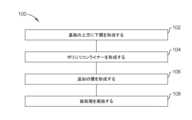
図1は、本開示の一実施形態による、基板を処理する方法100のフロー図である。方法100は、工程102で開始する。工程102では、一又は複数の下層が基板上に形成される。「基板(substrate)」は、製造プロセス中に表面上に膜処理が実施される任意の基板、又は基板上に形成された任意の材料面であり得る。例えば、処理が実行され得る基板表面には、用途に応じて、シリコン、酸化ケイ素、歪みシリコン、シリコン・オン・インシュレータ(SOI)、高濃度でドープされたシリコン、炭素がドープされた酸化ケイ素、アモルファスシリコン、ドープされたシリコン、ゲルマニウム、ヒ化ガリウム、ガラス、サファイアなどの材料、並びに金属、金属窒化物、金属合金、及びその他の導電性材料などの任意の他の材料が含まれる。高濃度にドープされたシリコンには、約0.1%以上のドーピングレベルでホウ素又はリンがドープされたシリコンが含まれ得る。基板は、半導体ウエハを含むが、これに限定されない。1 is a flow diagram of a
[0018]一又は複数の下層は、例えば、酸化ケイ素を含み得る。一例では、酸化ケイ素の下層は、アモルファス構造を有する。下層は、約100オングストロームから約2000オングストローム、例えば約200オングストロームから約1000オングストローム、又は例えば約300オングストロームから約500オングストロームの厚さまで形成される。しかしながら、他の厚さも想定される。[0018] The one or more underlayers may include, for example, silicon oxide. In one example, the silicon oxide underlayer has an amorphous structure. The underlayer is formed to a thickness of about 100 angstroms to about 2000 angstroms, such as about 200 angstroms to about 1000 angstroms, or for example about 300 angstroms to about 500 angstroms. However, other thicknesses are contemplated.
[0019]一又は複数の下層は、熱化学気相堆積(CVD)、熱原子層堆積(ALD)、プラズマ化学気相堆積(PECVD)、又はプラズマ原子層堆積(PEALD)を使用して形成され得る。適切な処理チャンバの一例は、カリフォルニア州サンタクララのApplied Materials, Inc.から入手可能なPrecision(TM)PECVD処理チャンバを含む。他の製造業者からのものを含む他の処理チャンバも使用され得ると想定される。[0019] The underlayer or underlayers may be formed using thermal chemical vapor deposition (CVD), thermal atomic layer deposition (ALD), plasma enhanced chemical vapor deposition (PECVD), or plasma enhanced atomic layer deposition (PEALD). An example of a suitable processing chamber includes the Precision™ PECVD processing chamber available from Applied Materials, Inc. of Santa Clara, Calif. It is contemplated that other processing chambers, including those from other manufacturers, may also be used.
[0020]続いて、工程104では、ポリシリコンライナーが一又は複数の下層の上面上に形成される。ポリシリコンライナーは、約1パーセントから約100パーセント、例えば約10パーセントから約90パーセント、又は約20パーセントから約80パーセント、又は約20パーセントから約70パーセント、又は約20パーセントから約60パーセント、又は約20パーセントから約50パーセント、又は約25パーセントから約40パーセント、又は約25パーセントから約35パーセントの結晶化度を有する。[0020] Then, in
[0021]一例では、ポリシリコンライナーは、PECVDプロセス中に形成される。PECVDプロセスは、容量結合プラズマ、誘導結合プラズマ、マイクロ波プラズマ、又は遠隔プラズマのうちの一又は複数を利用して、ポリシリコンライナーが一又は複数の下層の上面上に堆積するのを容易にする。ポリシリコンライナーは、約10オングストロームから約500オングストローム、例えば、約10オングストロームから約200オングストローム、又は約20オングストロームから約50オングストロームの範囲内の厚さまで形成される。ポリシリコンライナーは、一又は複数の下層と同じ処理チャンバ内に形成されてもよく、あるいは、ポリシリコンライナーは、一又は複数の下層とは異なるチャンバ内に形成されてもよい。[0021] In one example, the polysilicon liner is formed during a PECVD process. The PECVD process utilizes one or more of a capacitively coupled plasma, an inductively coupled plasma, a microwave plasma, or a remote plasma to facilitate deposition of the polysilicon liner on the top surface of the one or more underlayers. The polysilicon liner is formed to a thickness in a range of about 10 angstroms to about 500 angstroms, e.g., about 10 angstroms to about 200 angstroms, or about 20 angstroms to about 50 angstroms. The polysilicon liner may be formed in the same processing chamber as the one or more underlayers, or the polysilicon liner may be formed in a different chamber than the one or more underlayers.
[0022]ポリシリコンライナーの形成中、一又は複数の処理ガスが処理チャンバへ導入され、そのラジカルがプラズマ励起を介して生成される。一又は複数の処理ガスには、シリコン源、並びに任意選択的な還元剤及び任意選択的なキャリアガス又は他の不活性ガスが含まれる。このような例では、処理ガスは、シラン又は高次シラン(例えば、SinH2n+2;ここでnは1以上の整数である)を含む。処理ガスは、水素、例えば二原子水素、及びヘリウム、アルゴン等のキャリアガスを含み得る。シランは、300ミリメートル(mm)の基板について、約10sccmから約38sccm、例えば約15sccmから約30sccmの範囲内の流量で、処理チャンバの内部空間に提供される。水素は、300mmの基板について、約500sccmから約3500sccm、又は約1000sccmから約1500sccmの範囲内の流量で、処理チャンバの内部空間に提供される。キャリアガスは、約0sccmから約1000sccm、例えば、約50sccmから約600sccm、又は約200sccmから約300sccmの流量で提供され得る。約300ワットから約2700ワット、例えば約1000ワットから約1500ワットの高周波RF電力が、処理ガスに印加されて、処理ガスのラジカルが生成される。 [0022] During the formation of the polysilicon liner, one or more process gases are introduced into the process chamber, and the radicals are generated through plasma excitation. The one or more process gases include a silicon source, and an optional reducing agent and an optional carrier gas or other inert gas. In such an example, the process gas includes silane or higher silane (e.g., Sin H2n+2 ; where n is an integer equal to or greater than 1). The process gas may include hydrogen, e.g., diatomic hydrogen, and a carrier gas, such as helium, argon, etc. Silane is provided to the interior space of the process chamber at a flow rate in the range of about 10 sccm to about 38 sccm, e.g., about 15 sccm to about 30 sccm, for a 300 millimeter (mm) substrate. Hydrogen is provided to the interior space of the process chamber at a flow rate in the range of about 500 sccm to about 3500 sccm, or about 1000 sccm to about 1500 sccm, for a 300 mm substrate. The carrier gas may be provided at a flow rate of about 0 sccm to about 1000 sccm, for example, about 50 sccm to about 600 sccm, or about 200 sccm to about 300 sccm. High frequency RF power of about 300 Watts to about 2700 Watts, for example, about 1000 Watts to about 1500 Watts, is applied to the process gas to generate radicals in the process gas.
[0023]ポリシリコンライナーの堆積中、チャンバ内の圧力は、約0.5Torrから約10Torr、例えば約1Torrから約5Torrの範囲内で維持される。堆積中、基板は、約300℃から約500℃の温度、例えば約350℃から約450℃で維持される。堆積プロセスは、所定の厚さのポリシリコンライナーが堆積するのに十分な期間続いてもよい。例えば、堆積時間は、約30秒間から約1800秒間、例えば約60秒間から約180秒間続いてもよい。[0023] During deposition of the polysilicon liner, the pressure in the chamber is maintained within a range of about 0.5 Torr to about 10 Torr, e.g., about 1 Torr to about 5 Torr. During deposition, the substrate is maintained at a temperature of about 300°C to about 500°C, e.g., about 350°C to about 450°C. The deposition process may continue for a period of time sufficient to deposit a predetermined thickness of the polysilicon liner. For example, the deposition time may last from about 30 seconds to about 1800 seconds, e.g., from about 60 seconds to about 180 seconds.
[0024]別の例では、ポリシリコンライナーは、熱CVDなどの熱堆積プロセス中に形成される。ポリシリコンライナーは、約50オングストロームから約200オングストロームの範囲内の厚さまで形成される。堆積は、約350℃から約650℃の温度、例えば約500℃と650℃の間の温度で、かつポリシリコンライナーが所定の厚さまで堆積するのに十分な期間生じる。上記のものと同様の前駆体が、熱CVD工程中に利用され得る。[0024] In another example, the polysilicon liner is formed during a thermal deposition process, such as thermal CVD. The polysilicon liner is formed to a thickness within a range of about 50 angstroms to about 200 angstroms. The deposition occurs at a temperature of about 350° C. to about 650° C., for example, between about 500° C. and 650° C., and for a period of time sufficient for the polysilicon liner to be deposited to a predetermined thickness. Precursors similar to those described above may be utilized during the thermal CVD process.
[0025]別の例では、ポリシリコンライナーは、PECVDプロセス、又は熱CVDなどの熱堆積プロセスと、その後の結晶化アニーリングプロセス中にアモルファスシリコン層の堆積によって形成される。アモルファスシリコン層は、上記のものと同様のプロセス条件を使用して堆積され得る。アモルファスシリコン層は、シランなどの一又は複数のシリコン前駆体を含む処理ガス、キャリアガス、及び還元剤を使用することによって形成され得る。アモルファスシリコン層は、低水素アモルファスシリコン、例えば、1パーセント未満のアモルファスシリコンであり得る。アモルファスシリコン層は、約10オングストロームから約1000オングストローム、例えば、約10オングストロームから約500オングストローム、又は約50オングストロームから約100オングストロームの範囲内の厚さまで形成される。アモルファスシリコン層は、結晶化アニーリングを使用してさらに処理される。結晶化アニーリングプロセスは、1時間と4時間の間、例えば約1時間と2時間の間の期間、約600℃から約650℃の温度での熱アニーリングであり得る。別の例では、結晶化アニーリングプロセスは、急速熱アニーリング処理チャンバを使用するスパイクアニーリングプロセスであり得る。スパイクアニーリングプロセスは、約1秒間から約5秒間、約900℃から約1100℃の温度、例えば1000℃であり得る。アニーリングプロセスは、工程102で形成された下層の上面へのポリシリコンライナーの接着を強化する。[0025] In another example, the polysilicon liner is formed by deposition of an amorphous silicon layer during a thermal deposition process, such as a PECVD process or thermal CVD, followed by a crystallization annealing process. The amorphous silicon layer may be deposited using process conditions similar to those described above. The amorphous silicon layer may be formed by using a process gas including one or more silicon precursors, such as silane, a carrier gas, and a reducing agent. The amorphous silicon layer may be low hydrogen amorphous silicon, e.g., less than 1 percent amorphous silicon. The amorphous silicon layer is formed to a thickness in the range of about 10 angstroms to about 1000 angstroms, e.g., about 10 angstroms to about 500 angstroms, or about 50 angstroms to about 100 angstroms. The amorphous silicon layer is further processed using a crystallization annealing. The crystallization annealing process can be a thermal annealing at a temperature of about 600° C. to about 650° C. for a period of between 1 and 4 hours, e.g., between about 1 and 2 hours. In another example, the crystallization annealing process can be a spike annealing process using a rapid thermal annealing processing chamber. The spike annealing process can be at a temperature of about 900° C. to about 1100° C., e.g., 1000° C., for a period of about 1 second to about 5 seconds. The annealing process strengthens the adhesion of the polysilicon liner to the top surface of the underlayer formed in
[0026]工程106では、一又は複数の追加の層が、ポリシリコンライナーの上面上に形成される。一又は複数の追加の層には、例えば、ドープされたか又はドープされていないアモルファスシリコンが含まれる。特定の例では、一又は複数の追加の層は、積層で、n型にドープされた(例えば、リン)アモルファスシリコンとドープされていないアモルファスシリコンが交互になった層を含む。別の例では、一又は複数の追加の層は、積層で、p型にドープされた(例えば、ホウ素)アモルファスシリコンとドープされていないアモルファスシリコンが交互になった層を含む。別の例では、一又は複数の追加の層は、p型にドープされたアモルファスシリコン又はn型にドープされたアモルファスシリコンの単一層である。一又は複数の追加の層は、シラン等の一又は複数のシリコン前駆体を含む処理ガス、キャリアガス、還元剤、及びホスフィン等のn型ドーパントといったドーパントを使用して、PECVDチャンバ内に形成され得る。一又は複数の追加の層は、一又は複数の後処理工程を通じて、メモリデバイスなどの半導体デバイスの形成を容易にする。一又は複数の追加の層は、ポリシリコンライナーと同じ処理チャンバ内で、又は異なる処理チャンバ内に形成され得る。[0026] In
[0027]工程108では、下層、ポリシリコンライナー、及びその上の一又は複数の追加の層を有する基板(本明細書ではデバイス中間体とも呼ばれる)上で、一又は複数の後処理が実施される。後処理工程は、とりわけ、さらなる堆積プロセス、エッチングプロセス、マスキング、エッチング、リソグラフィ、ドーピング、熱処理、及び研磨を含む。特定の一例では、その上に堆積された層を有するデバイス中間体は、アニーリングなどの熱処理プロセスに供される。熱アニーリングプロセスは、デバイス中間体内の膜欠陥の修復を容易にし、また、個別の層内のドーパント種の分布さえも容易にする。[0027] In
[0028]図1は、基板を処理する一方法について記載しているが、他の実施態様も想定される。例えば、天然酸化物除去プロセス、又は別の洗浄プロセスが、工程102の前に生じ得ることが想定される。このような例では、天然酸化物除去プロセス又は他の洗浄プロセスは、工程102及び/又は104及び/又は106と同じチャンバ内で生じてもよく、工程102及び/又は104及び/又は106とは異なるチャンバ内で生じてもよい。本明細書中の他の例及び実施形態と組み合わせることができる別の例では、工程106の一又は複数の追加の層は、PECVDではなく熱堆積プロセスを介して形成され得る。1 describes one method of processing a substrate, other implementations are contemplated. For example, it is contemplated that a native oxide removal process, or another cleaning process, may occur prior to step 102. In such an example, the native oxide removal process or another cleaning process may occur in the same chamber as
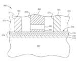
[0029]図2は、図1の方法100に方法によって形成されたデバイス中間体210の概略断面図である。本明細書で使用されるデバイス中間体は、製造中のデバイス、例えば、製造完了前のデイバスを指す。デバイス中間体210は、基板212及び中間積層体222を含む。中間積層体222は、基板212の上方に形成された一又は複数の下層214(明確にするために1つが示されている)を含む。中間積層体222は、一又は複数の下層214上に形成されたポリシリコンライナー216、及びポリシリコンライナー216上に形成された一又は複数のアモルファスシリコン層218(明確にするために1つが示されている)も含む。デバイス中間体210は明確にするためにここでは示されていない他の特徴も含み得ることが、想定される。2 is a schematic cross-sectional view of a device intermediate 210 formed by the
[0030]デバイス中間体210の後処理中(すなわち、工程108)を含む基板の処理中、及び/又は一又は複数の追加の層218の形成中(すなわち、工程106)、水素は、堆積された膜内に及び膜境界を横断して分散する。水素は、(1)一又は複数の下層214における酸化ケイ素中の水素濃度と比べて一又は複数の追加の層218におけるアモルファスシリコン層中の比較的高い水素濃度、及び(2)処理及び/又は後処理中の高温を含む、一又は複数のメカニズムによって分散するよう導入される。アモルファスシリコンの比較的高い水素濃度と高温のうちの一方又は両方は、一又は複数の追加の層218のアモルファスシリコンから一又は複数の下層214のシリコンへの水素の移動を容易にする。シリコン(例えば、一又は複数の下層214)と比較してアモルファスシリコン(例えば、一又は複数の追加の層218)を通じた水素の分散速度は速いため、水素は、従来のデバイス構造体のシリコン及びアモルファスシリコンのインターフェースに蓄積する傾向がある。このような蓄積は、アモルファスシリコン-シリコンインターフェースで発生する水素泡をもたらし、ポリシリコンライナー216を含まない従来の構造におけるシリコン(例えば、一又は複数の下層)からのアモルファスシリコン(例えば、一又は複数の追加の層)の接着又は層剥離の減少をもたらす。[0030] During processing of the substrate, including during post-processing of the device intermediate 210 (i.e., step 108) and/or during formation of the one or more additional layers 218 (i.e., step 106), hydrogen diffuses within the deposited film and across film boundaries. Hydrogen is introduced to diffuse by one or more mechanisms, including (1) a relatively high hydrogen concentration in the amorphous silicon layer in the one or more
[0031]従来のアプローチ(一又は複数の追加の層のアモルファスシリコンを一又は複数の下層のうちの一つのシリコン上に直接堆積させる)とは対照的に、本開示の態様は、一又は複数の下層214上に配置されたポリシリコンライナー216を含む。ポリシリコンライナー216は、水素が一又は複数の追加の層から一又は複数の下層214の上面へ分散するのを防止する。よって、水素は、一又は複数の下層214の上面には蓄積せず、一又は複数の下層214の上面での気泡の形成は、緩和又は防止される。一又は複数の下層214の上面での水素気泡の形成が緩和又は防止されるため、膜積層体の接着が改善される。[0031] In contrast to conventional approaches (wherein one or more additional layers of amorphous silicon are deposited directly onto the silicon of one of the one or more underlying layers), aspects of the present disclosure include a
[0032]水素が一又は複数の追加の層218のインターフェース及びポリシリコンライナー216に分散しても、層剥離が生じるレベルまでは接着は概して減少されないことに留意されたい。これは、少なくとも部分的には、アモルファスシリコンとポリシリコンとの間の比較的高い接着による。よって、本明細書に記載される例では、水素は、比較的弱い接着インターフェース(例えば、アモルファスシリコンと酸化ケイ素との間)ではなく、比較的強い接着インターフェース(例えば、アモルファスシリコンとポリシリコンとの間)で蓄積する。[0032] It should be noted that even though hydrogen diffuses into the interfaces of one or more
[0033]図2を参照した上記のデバイス中間体は、金属-酸化物-シリコン電界効果トランスミッタ(MOSFET)デバイス等のメモリデバイスに使用される選択ビットトランジスタなどの、デバイス構造体のさまざまな部分に使用することができる。他の例では、図1及び図2を参照してデバイス中間体を形成するための方法は、磁気ランダムアクセスメモリ(MRAM)、スピン注入ランダムアクセスメモリ(STT-RAM)、強誘電体メモリ(FeRAM)、及び相変化メモリ(PCM)を含むメモリデバイス構造体等のデバイス構造体の一部であるデバイス中間体構造体を形成するのに有益であり得る。[0033] The device intermediates described above with reference to FIG. 2 can be used in various portions of device structures, such as select bit transistors used in memory devices, such as metal-oxide-silicon field effect transmitter (MOSFET) devices. In other examples, the methods for forming device intermediates with reference to FIGS. 1 and 2 can be useful for forming device intermediate structures that are part of device structures, such as memory device structures including magnetic random access memory (MRAM), spin transfer random access memory (STT-RAM), ferroelectric memory (FeRAM), and phase change memory (PCM).
[0034]図3Aは、薄膜トランジスタ(TFT)デバイス構造体310の一例を示す概略断面図である。デバイス構造体310は、図2に関して上に記載されるシリコン下層214とポリシリコンライナー216とアモルファスシリコン層218とを含む、デバイス中間体210及び中間積層体222を含むチャネル316を含む。デバイス構造体310は、基板212(例えば、ガラス、シリコン)、金属コンタクト314、及び基板212と金属接点314の上方のチャネル316を含む。チャネル316上には絶縁体層332(例えば、酸化ケイ素層)が堆積され、絶縁体層332上にはゲート金属層342が堆積される。[0034] Figure 3A is a schematic cross-sectional view of an example of a thin film transistor (TFT) device structure 310. The device structure 310 includes a
[0035]図3Bは、デバイス構造体350の一例を示す概略断面図である。デバイス構造体350は、MRAMデバイス、PCMデバイス、FeRAMデバイス、又は他の半導体デバイスの一部を形成し得る。デバイス構造体350は、図2に関して上に記載されるシリコン下層214とポリシリコンライナー216とアモルファスシリコン層218とを含む、デバイス中間体210及び中間積層体222を含むチャネル316を含む。デバイス構造体350は、基板351(例えば、シリコン、ゲルマニウム)及びチャネル316を含む。デバイス構造体350は、中間積層体222の上方に形成された電界酸化物370をさらに含む。電源コンタクト364がビア371に形成される。ビア372は、ゲート金属層356及びインターコネクト366を含む。絶縁体層354(例えば、酸化ケイ素)は、ゲート金属層356と中間積層体222との間に配置される。ドレインコンタクト362がビア373に形成される。3B is a schematic cross-sectional view of an example of a
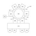
[0036]図4は、本明細書に記載されるような、デバイス構造体を形成する方法が実施され得る例示的な真空処理システム400の概略上面図を示す。このシステム400は、ウエハ上の集積回路等の真空において、処理された基板を製造するために使用される、クラスタータイプのシステムである。真空処理システム400は、典型的にはプラットフォーム(図示せず)上に取り付けられた移送チャンバ402を含む。移送チャンバはシステムコントローラ401に接続され、システムコントローラ401は、本明細書で開示される主題の態様を収納及び/又は実装するよう構成されている。移送チャンバ402は、その上に取り付けられたリッド403を有する。リッド403が接着されているとき、移送チャンバ内の圧力が真空に減少したときに空気が移送チャンバ402へ漏れないように、リッド403は移送チャンバ402との気密密封を形成する。移送チャンバ402は、ファセット406に接着された処理チャンバ404を有する。処理チャンバ404は、物理的気相堆積チャンバ、CVDチャンバ、ALDチャンバ、PECVDチャンバ、PEALDチャンバ、エッチングチャンバ等のあらゆるタイプの処理チャンバであり得る。処理チャンバ404は、個別の処理チャンバ404の構成に応じて、移送チャンバ402によって支持されていてもよく、又はそれら自体のプラットフォーム上に支持されていてもよい。ファセット406中のスリットバルブ(図示せず)は、移送チャンバ402と処理チャンバ404との間のアクセス及び分離を提供する。それに応じて、処理チャンバ404は、その表面上に開口部(図示せず)を有し、開口部はスリットバルブと整列している。移送チャンバ402は、ファセット412に取り付けられたロードロックチャンバ408も有する。ファセット412中の開口部(図示せず)は、ロードロックチャンバ408と移送チャンバ402との間のアクセス及び分離を提供する。それに応じて、ロードロックチャンバ408はその表面上に開口部を有し、開口部はファセット412中の開口部と整列している。[0036] FIG. 4 shows a schematic top view of an exemplary
[0037]ロードロックチャンバ408は、小環境414に接着されている。ロードロックチャンバ408及び小環境414は、ロードロックチャンバと小環境との間のアクセスを提供する対応する開口部(図示せず)を有し、その一方、開口部のドア(図示せず)は分離を提供する。小環境は、その前面に接着されたポッドローダ416を有する。対応するドア(図示せず)を有する開口部(図示せず)は、小環境414とポッドローダ416との間のアクセス及び分離を提供する。[0037] The
[0038]工程では、システム400内の処理される基板は、ポッドローダ416の頂部に置かれる。その後、ロボット(図示せず)は、一度に一つずつ、ポッドローダ416から出し、ロードロックチャンバ408のうちの一つへ入れて、基板の除去を開始する。基板がロードロックチャンバ408内にロードされた後、ロードロックチャンバの圧力は、移送チャンバ402の圧力と一致するよう低減される。その後、移送チャンバ側のドアが開けられ、移送チャンバロボット(図示せず)は、ロードロックチャンバ408の点検を開始することができる。移送チャンバロボットは、処理のために基板をロードロックチャンバ408から処理チャンバ404のうちの一つへ移動させ、その後、ロードロックチャンバ408のうちの一つから基板を戻す。ロードロックチャンバ408が処理された基板の全てを受領したとき、ロードロックチャンバ内の圧力は小環境の圧力に戻され、そのため、小環境内のロボットは、処理された基板を基板ポッドローダ416へ戻すことができる。In the process, the substrates to be processed in the
[0039]以上の記述は本開示の実施形態を対象としているが、本開示の基本的な範囲から逸脱することなく本開示の他の実施形態及び更なる実施形態が考案されてよく、本開示の範囲は、下記の特許請求の範囲によって決定される。[0039] While the foregoing is directed to embodiments of the present disclosure, other and further embodiments of the present disclosure may be devised without departing from the basic scope thereof, the scope of which is determined by the claims which follow.
Claims (9)
Translated fromJapanese酸化ケイ素を含む下層を基板の上方に堆積させることと、
約10sccmから約38sccmの範囲内の流量で、30秒間から1800秒間の時間にわたり、約300℃から約500℃の温度で、前記基板にシリコン源を提供することによって、前記下層上にポリシリコンライナーを堆積させることであって、前記ポリシリコンライナーが約25パーセントから約40パーセントの結晶化度を有するまで行われる、ポリシリコンライナーを堆積させることと、
アモルファスシリコン層を前記ポリシリコンライナー上に堆積させることと、
を含む、方法。 1. A method comprising:
depositing an underlayer comprising silicon oxide over a substrate;
depositing a polysilicon liner on the underlayer by providing a silicon source to the substrate at a temperature of about 300° C. to about 500° C. for a time period of 30 seconds to 1800 seconds at a flow rate in a range of about 10 sccm to about 38 sccm, wherein the polysilicon liner has a crystallinity of about 25 percent to about 40 percent;
depositing an amorphous silicon layer over the polysilicon liner;
A method comprising:
酸化ケイ素を含む下層を基板の上方に堆積させることと、
約10sccmから約38sccmの範囲内の流量で、30秒間から1800秒間の時間にわたり、約300℃から約500℃の温度で、前記基板にシリコン源を提供することによって、前記下層上にポリシリコンライナーを堆積させることであって、前記ポリシリコンライナーが約25パーセントから約40パーセントの結晶化度を有するまで行われ、前記下層を堆積させるのと同じチャンバ内で実施される、ポリシリコンライナーを堆積させることと、
アモルファスシリコン層を前記ポリシリコンライナー上に堆積させることと、
を含む、方法。 1. A method of forming a device intermediate, comprising:
depositing an underlayer comprising silicon oxide over a substrate;
depositing a polysilicon liner on the underlayer by providing a silicon source to the substrate at a temperature of about 300° C. to about 500° C. for a time period of 30 seconds to 1800 seconds at a flow rate in a range of about 10 sccm to about 38 sccm, until the polysilicon liner has a crystallinity of about 25 percent to about 40 percent, the deposition being performed in the same chamber as depositing the underlayer;
depositing an amorphous silicon layer over the polysilicon liner;
A method comprising:
Applications Claiming Priority (3)
| Application Number | Priority Date | Filing Date | Title |
|---|---|---|---|
| US201962807614P | 2019-02-19 | 2019-02-19 | |
| US62/807,614 | 2019-02-19 | ||
| PCT/US2020/018854WO2020172299A1 (en) | 2019-02-19 | 2020-02-19 | Polysilicon liners |
Publications (2)
| Publication Number | Publication Date |
|---|---|
| JP2022523171A JP2022523171A (en) | 2022-04-21 |
| JP7611837B2true JP7611837B2 (en) | 2025-01-10 |
Family
ID=72043674
Family Applications (1)
| Application Number | Title | Priority Date | Filing Date |
|---|---|---|---|
| JP2021547411AActiveJP7611837B2 (en) | 2019-02-19 | 2020-02-19 | Polysilicon Liner |
Country Status (7)
| Country | Link |
|---|---|
| US (1) | US11170990B2 (en) |
| JP (1) | JP7611837B2 (en) |
| KR (1) | KR102822599B1 (en) |
| CN (1) | CN113454755A (en) |
| SG (1) | SG11202108406RA (en) |
| TW (2) | TW202425082A (en) |
| WO (1) | WO2020172299A1 (en) |
Citations (4)
| Publication number | Priority date | Publication date | Assignee | Title |
|---|---|---|---|---|
| JP2011187609A (en) | 2010-03-08 | 2011-09-22 | Seiko Epson Corp | Method of manufacturing semiconductor device, electro-optical apparatus, and electronic apparatus |
| JP2012014099A (en) | 2010-07-05 | 2012-01-19 | Mitsubishi Electric Corp | Active matrix substrate and liquid crystal device |
| WO2012127769A1 (en) | 2011-03-22 | 2012-09-27 | パナソニック株式会社 | Method for forming semiconductor thin film, semiconductor device, method for producing semiconductor device, substrate, and thin film substrate |
| WO2013021416A1 (en) | 2011-08-09 | 2013-02-14 | パナソニック株式会社 | Thin film semiconductor device and method for manufacturing thin film semiconductor device |
Family Cites Families (30)
| Publication number | Priority date | Publication date | Assignee | Title |
|---|---|---|---|---|
| EP0383230B1 (en)* | 1989-02-14 | 1997-05-28 | Seiko Epson Corporation | Manufacturing Method of a Semiconductor Device |
| JP3173747B2 (en)* | 1992-10-09 | 2001-06-04 | 株式会社半導体エネルギー研究所 | Method for manufacturing semiconductor device |
| US5326722A (en)* | 1993-01-15 | 1994-07-05 | United Microelectronics Corporation | Polysilicon contact |
| JP3344072B2 (en)* | 1994-03-31 | 2002-11-11 | ソニー株式会社 | Method for manufacturing thin film transistor |
| DE19710487A1 (en)* | 1996-03-13 | 1997-09-18 | Toshiba Kawasaki Kk | Semiconductor module with vertical semiconductor component |
| US5882962A (en)* | 1996-07-29 | 1999-03-16 | Vanguard International Semiconductor Corporation | Method of fabricating MOS transistor having a P+ -polysilicon gate |
| KR100220253B1 (en)* | 1996-12-27 | 1999-09-15 | 김영환 | Method of manufacturing mosfet |
| GB2322733A (en)* | 1997-02-27 | 1998-09-02 | Nec Corp | Polysilicon electrodes for DRAM cells |
| US5976959A (en)* | 1997-05-01 | 1999-11-02 | Industrial Technology Research Institute | Method for forming large area or selective area SOI |
| US6352594B2 (en)* | 1997-08-11 | 2002-03-05 | Torrex | Method and apparatus for improved chemical vapor deposition processes using tunable temperature controlled gas injectors |
| JPH11150283A (en)* | 1997-11-19 | 1999-06-02 | Tdk Corp | Manufacture of polycrystalline silicon thin film |
| US6482749B1 (en)* | 2000-08-10 | 2002-11-19 | Seh America, Inc. | Method for etching a wafer edge using a potassium-based chemical oxidizer in the presence of hydrofluoric acid |
| CN1407603A (en)* | 2001-08-25 | 2003-04-02 | 日立电线株式会社 | Crystal silicon film semiconductor device and its manufacture, and photoelectric device |
| US6700906B2 (en)* | 2002-01-31 | 2004-03-02 | The Regents Of The University Of California | High energy, high average power solid state green or UV laser |
| US7119365B2 (en)* | 2002-03-26 | 2006-10-10 | Sharp Kabushiki Kaisha | Semiconductor device and manufacturing method thereof, SOI substrate and display device using the same, and manufacturing method of the SOI substrate |
| CN1317735C (en)* | 2003-01-23 | 2007-05-23 | 友达光电股份有限公司 | Buffer layer capable of promoting improvement of electron mobility and thin film transistor comprising the layer |
| KR20050054788A (en) | 2003-12-06 | 2005-06-10 | 삼성전자주식회사 | Fabrication method of poly-crystalline si thin film and transistor thereby |
| CN1630036A (en)* | 2003-12-17 | 2005-06-22 | 旺宏电子股份有限公司 | Semiconductor element and method of manufacturing polysilicon layer formed therein |
| KR100666563B1 (en)* | 2004-07-05 | 2007-01-09 | 삼성에스디아이 주식회사 | Method for manufacturing semiconductor device and semiconductor device manufactured by this method |
| KR101239108B1 (en)* | 2006-07-10 | 2013-03-06 | 주성엔지니어링(주) | Method for manufacturing polysilicon and method for manufactruing thin film transistor having the same |
| JP5161911B2 (en)* | 2010-03-25 | 2013-03-13 | 株式会社東芝 | Resistance change memory |
| CN103081093B (en)* | 2010-06-11 | 2015-06-03 | 科洛斯巴股份有限公司 | Pillar structure and method of memory device |
| US8088688B1 (en)* | 2010-11-05 | 2012-01-03 | Crossbar, Inc. | p+ polysilicon material on aluminum for non-volatile memory device and method |
| KR20120127009A (en)* | 2011-05-13 | 2012-11-21 | 에스케이하이닉스 주식회사 | Method for manufacturing semiconductor device |
| JP2013084902A (en) | 2011-09-26 | 2013-05-09 | Dainippon Screen Mfg Co Ltd | Heat treatment method and heat treatment apparatus |
| CN103828061B (en)* | 2011-10-07 | 2018-02-13 | 应用材料公司 | Carry out the method for deposit silicon-containing materials using argon-dilution |
| CN103060768A (en)* | 2013-01-17 | 2013-04-24 | 云南师范大学 | Low-temperature rapid crystallization method for amorphous silicon film |
| KR20160083049A (en) | 2013-11-04 | 2016-07-11 | 어플라이드 머티어리얼스, 인코포레이티드 | Adhesion improvements for oxide-silicon stack |
| CN107636839B (en)* | 2016-07-25 | 2020-12-04 | 京东方科技集团股份有限公司 | Polysilicon thin film transistor, method for manufacturing the same, and display device |
| CN110085550A (en)* | 2018-01-26 | 2019-08-02 | 沈阳硅基科技有限公司 | A kind of semiconductor product insulation layer structure and preparation method thereof |
- 2020
- 2020-02-19TWTW113101360Apatent/TW202425082A/enunknown
- 2020-02-19JPJP2021547411Apatent/JP7611837B2/enactiveActive
- 2020-02-19TWTW109105294Apatent/TWI831926B/enactive
- 2020-02-19CNCN202080015255.9Apatent/CN113454755A/enactivePending
- 2020-02-19USUS16/795,191patent/US11170990B2/enactiveActive
- 2020-02-19KRKR1020217029817Apatent/KR102822599B1/enactiveActive
- 2020-02-19SGSG11202108406RApatent/SG11202108406RA/enunknown
- 2020-02-19WOPCT/US2020/018854patent/WO2020172299A1/ennot_activeCeased
Patent Citations (4)
| Publication number | Priority date | Publication date | Assignee | Title |
|---|---|---|---|---|
| JP2011187609A (en) | 2010-03-08 | 2011-09-22 | Seiko Epson Corp | Method of manufacturing semiconductor device, electro-optical apparatus, and electronic apparatus |
| JP2012014099A (en) | 2010-07-05 | 2012-01-19 | Mitsubishi Electric Corp | Active matrix substrate and liquid crystal device |
| WO2012127769A1 (en) | 2011-03-22 | 2012-09-27 | パナソニック株式会社 | Method for forming semiconductor thin film, semiconductor device, method for producing semiconductor device, substrate, and thin film substrate |
| WO2013021416A1 (en) | 2011-08-09 | 2013-02-14 | パナソニック株式会社 | Thin film semiconductor device and method for manufacturing thin film semiconductor device |
Also Published As
| Publication number | Publication date |
|---|---|
| JP2022523171A (en) | 2022-04-21 |
| KR102822599B1 (en) | 2025-06-19 |
| US20200266052A1 (en) | 2020-08-20 |
| KR20210118236A (en) | 2021-09-29 |
| CN113454755A (en) | 2021-09-28 |
| TW202046377A (en) | 2020-12-16 |
| SG11202108406RA (en) | 2021-09-29 |
| TW202425082A (en) | 2024-06-16 |
| US11170990B2 (en) | 2021-11-09 |
| TWI831926B (en) | 2024-02-11 |
| WO2020172299A1 (en) | 2020-08-27 |
Similar Documents
| Publication | Publication Date | Title |
|---|---|---|
| US7473655B2 (en) | Method for silicon based dielectric chemical vapor deposition | |
| US7910497B2 (en) | Method of forming dielectric layers on a substrate and apparatus therefor | |
| US20080014759A1 (en) | Method for fabricating a gate dielectric layer utilized in a gate structure | |
| US7501349B2 (en) | Sequential oxide removal using fluorine and hydrogen | |
| US10615050B2 (en) | Methods for gapfill in high aspect ratio structures | |
| US20080026553A1 (en) | Method for fabricating an integrated gate dielectric layer for field effect transistors | |
| WO2017223323A1 (en) | Flowable amorphous silicon films for gapfill applications | |
| TWI871500B (en) | Mosfet gate engineerinng with dipole films | |
| WO2003060184A9 (en) | Method and apparatus for forming silicon containing films | |
| CN101151712A (en) | Method and system for removing oxide from a substrate | |
| US20080274626A1 (en) | Method for depositing a high quality silicon dielectric film on a germanium substrate with high quality interface | |
| KR20090027162A (en) | Deformation of polycrystalline polysilicon films and peripheral layers through the use of multilayer silicon films and dopants having a controlled crystal structure | |
| US20010012667A1 (en) | Clustered system and method for formation of integrated circuit devices | |
| WO2007021403A2 (en) | Low-temperature oxide removal using fluorine | |
| US6635556B1 (en) | Method of preventing autodoping | |
| JP2022511814A (en) | How to reduce the effective oxide thickness of semiconductor structures | |
| JP7611837B2 (en) | Polysilicon Liner | |
| US10593543B2 (en) | Method of depositing doped amorphous silicon films with enhanced defect control, reduced substrate sensitivity to in-film defects and bubble-free film growth | |
| JP4224044B2 (en) | Manufacturing method of semiconductor device | |
| JP2000150901A (en) | Method for manufacturing thin film semiconductor device |
Legal Events
| Date | Code | Title | Description |
|---|---|---|---|
| A621 | Written request for application examination | Free format text:JAPANESE INTERMEDIATE CODE: A621 Effective date:20230214 | |
| A977 | Report on retrieval | Free format text:JAPANESE INTERMEDIATE CODE: A971007 Effective date:20240219 | |
| A131 | Notification of reasons for refusal | Free format text:JAPANESE INTERMEDIATE CODE: A131 Effective date:20240227 | |
| A521 | Request for written amendment filed | Free format text:JAPANESE INTERMEDIATE CODE: A523 Effective date:20240523 | |
| A131 | Notification of reasons for refusal | Free format text:JAPANESE INTERMEDIATE CODE: A131 Effective date:20240716 | |
| A521 | Request for written amendment filed | Free format text:JAPANESE INTERMEDIATE CODE: A523 Effective date:20241015 | |
| TRDD | Decision of grant or rejection written | ||
| A01 | Written decision to grant a patent or to grant a registration (utility model) | Free format text:JAPANESE INTERMEDIATE CODE: A01 Effective date:20241126 | |
| A61 | First payment of annual fees (during grant procedure) | Free format text:JAPANESE INTERMEDIATE CODE: A61 Effective date:20241224 | |
| R150 | Certificate of patent or registration of utility model | Ref document number:7611837 Country of ref document:JP Free format text:JAPANESE INTERMEDIATE CODE: R150 |