JP7611536B2 - Light control device - Google Patents
Light control deviceDownload PDFInfo
- Publication number
- JP7611536B2 JP7611536B2JP2023126703AJP2023126703AJP7611536B2JP 7611536 B2JP7611536 B2JP 7611536B2JP 2023126703 AJP2023126703 AJP 2023126703AJP 2023126703 AJP2023126703 AJP 2023126703AJP 7611536 B2JP7611536 B2JP 7611536B2
- Authority
- JP
- Japan
- Prior art keywords
- unit
- power supply
- control
- period
- state
- Prior art date
- Legal status (The legal status is an assumption and is not a legal conclusion. Google has not performed a legal analysis and makes no representation as to the accuracy of the status listed.)
- Active
Links
Images


Classifications
- H—ELECTRICITY
- H05—ELECTRIC TECHNIQUES NOT OTHERWISE PROVIDED FOR
- H05B—ELECTRIC HEATING; ELECTRIC LIGHT SOURCES NOT OTHERWISE PROVIDED FOR; CIRCUIT ARRANGEMENTS FOR ELECTRIC LIGHT SOURCES, IN GENERAL
- H05B45/00—Circuit arrangements for operating light-emitting diodes [LED]
- H05B45/10—Controlling the intensity of the light
- H—ELECTRICITY
- H05—ELECTRIC TECHNIQUES NOT OTHERWISE PROVIDED FOR
- H05B—ELECTRIC HEATING; ELECTRIC LIGHT SOURCES NOT OTHERWISE PROVIDED FOR; CIRCUIT ARRANGEMENTS FOR ELECTRIC LIGHT SOURCES, IN GENERAL
- H05B47/00—Circuit arrangements for operating light sources in general, i.e. where the type of light source is not relevant
- H05B47/10—Controlling the light source
- H—ELECTRICITY
- H03—ELECTRONIC CIRCUITRY
- H03K—PULSE TECHNIQUE
- H03K17/00—Electronic switching or gating, i.e. not by contact-making and –breaking
- H03K17/51—Electronic switching or gating, i.e. not by contact-making and –breaking characterised by the components used
- H03K17/56—Electronic switching or gating, i.e. not by contact-making and –breaking characterised by the components used by the use, as active elements, of semiconductor devices
- H03K17/687—Electronic switching or gating, i.e. not by contact-making and –breaking characterised by the components used by the use, as active elements, of semiconductor devices the devices being field-effect transistors
- H03K17/6871—Electronic switching or gating, i.e. not by contact-making and –breaking characterised by the components used by the use, as active elements, of semiconductor devices the devices being field-effect transistors the output circuit comprising more than one controlled field-effect transistor
- H—ELECTRICITY
- H05—ELECTRIC TECHNIQUES NOT OTHERWISE PROVIDED FOR
- H05B—ELECTRIC HEATING; ELECTRIC LIGHT SOURCES NOT OTHERWISE PROVIDED FOR; CIRCUIT ARRANGEMENTS FOR ELECTRIC LIGHT SOURCES, IN GENERAL
- H05B39/00—Circuit arrangements or apparatus for operating incandescent light sources
- H05B39/04—Controlling
- H05B39/041—Controlling the light-intensity of the source
- H05B39/044—Controlling the light-intensity of the source continuously
- H05B39/048—Controlling the light-intensity of the source continuously with reverse phase control
- H—ELECTRICITY
- H05—ELECTRIC TECHNIQUES NOT OTHERWISE PROVIDED FOR
- H05B—ELECTRIC HEATING; ELECTRIC LIGHT SOURCES NOT OTHERWISE PROVIDED FOR; CIRCUIT ARRANGEMENTS FOR ELECTRIC LIGHT SOURCES, IN GENERAL
- H05B41/00—Circuit arrangements or apparatus for igniting or operating discharge lamps
- H05B41/14—Circuit arrangements
- H05B41/36—Controlling
- H05B41/38—Controlling the intensity of light
- H05B41/39—Controlling the intensity of light continuously
- H05B41/392—Controlling the intensity of light continuously using semiconductor devices, e.g. thyristor
- H05B41/3921—Controlling the intensity of light continuously using semiconductor devices, e.g. thyristor with possibility of light intensity variations
- H05B41/3924—Controlling the intensity of light continuously using semiconductor devices, e.g. thyristor with possibility of light intensity variations by phase control, e.g. using a triac
- Y—GENERAL TAGGING OF NEW TECHNOLOGICAL DEVELOPMENTS; GENERAL TAGGING OF CROSS-SECTIONAL TECHNOLOGIES SPANNING OVER SEVERAL SECTIONS OF THE IPC; TECHNICAL SUBJECTS COVERED BY FORMER USPC CROSS-REFERENCE ART COLLECTIONS [XRACs] AND DIGESTS
- Y02—TECHNOLOGIES OR APPLICATIONS FOR MITIGATION OR ADAPTATION AGAINST CLIMATE CHANGE
- Y02B—CLIMATE CHANGE MITIGATION TECHNOLOGIES RELATED TO BUILDINGS, e.g. HOUSING, HOUSE APPLIANCES OR RELATED END-USER APPLICATIONS
- Y02B20/00—Energy efficient lighting technologies, e.g. halogen lamps or gas discharge lamps
- Y02B20/40—Control techniques providing energy savings, e.g. smart controller or presence detection
Landscapes
- Circuit Arrangement For Electric Light Sources In General (AREA)
Description
Translated fromJapanese本発明は、照明負荷を調光する調光装置に関する。The present invention relates to a dimming device that dims a lighting load.
従来、照明負荷を調光する調光装置が知られている(例えば、特許文献1)。Conventionally, a dimming device that dims a lighting load is known (for example, Patent Document 1).
特許文献1に記載された調光装置は、一対の端子と、制御回路部と、制御回路部に制御電源を供給する制御電源部と、照明負荷の調光レベルを設定する調光操作部とを備えている。The dimming device described in
一対の端子間には、制御回路部及び制御電源部それぞれが並列に接続されている。また、一対の端子間には、交流電源と照明負荷との直列回路が接続される。照明負荷は、複数のLED(Light Emitting Diode)素子と、各LED素子を点灯させる電源回路とを備えている。電源回路は、ダイオードと電解コンデンサとの平滑回路を備えている。A control circuit section and a control power supply section are connected in parallel between a pair of terminals. A series circuit of an AC power supply and a lighting load is also connected between the pair of terminals. The lighting load includes a number of LED (Light Emitting Diode) elements and a power supply circuit that lights up each of the LED elements. The power supply circuit includes a smoothing circuit of a diode and an electrolytic capacitor.
制御回路部は、照明負荷に供給する交流電圧を位相制御するスイッチ部と、スイッチ部を駆動するスイッチドライブ部と、スイッチドライブ部及び制御電源部を制御する制御部と、を備えている。The control circuit unit includes a switch unit that phase controls the AC voltage supplied to the lighting load, a switch drive unit that drives the switch unit, and a control unit that controls the switch drive unit and the control power supply unit.
制御電源部は、スイッチ部に並列に接続されている。制御電源部は、交流電源の交流電圧を制御電源に変換する。制御電源部は、制御電源を蓄積する電解コンデンサを備えている。The control power supply unit is connected in parallel to the switch unit. The control power supply unit converts the AC voltage of the AC power supply into the control power supply. The control power supply unit is equipped with an electrolytic capacitor that stores the control power supply.
制御部は、制御電源部から電解コンデンサを通じて制御電源が供給される。制御部は、マイクロコンピュータを備えている。マイクロコンピュータは、調光操作部で設定された調光レベルに応じて、交流電圧の半サイクル毎の期間途中で、照明負荷への給電を遮断する逆位相制御を行う。The control unit is supplied with control power from the control power supply unit through an electrolytic capacitor. The control unit is equipped with a microcomputer. The microcomputer performs reverse phase control to cut off the power supply to the lighting load midway through each half cycle of the AC voltage, depending on the dimming level set by the dimming operation unit.
本発明は、より多くの種類の負荷に対応可能な調光装置を提供することを目的とする。The present invention aims to provide a dimmer device that can handle a wider variety of loads.
本発明の一態様に係る調光装置は、負荷と交流電源との間に電気的に接続される一対の入力端子と、前記一対の入力端子間において、双方向の電流の遮断と通過とを切り替え可能であり、制御可能な2つの半導体スイッチを備える双方向スイッチと、調光レベルが入力される入力部と、前記調光レベルに応じて前記双方向スイッチを制御する制御部と、前記交流電源から電力供給され前記制御部の電源を生成する制御電源部と、を備える。前記制御部は、前記交流電源の交流電圧の半周期の区間において、前記調光レベルに応じて前記2つの半導体スイッチの両方の制御信号を第一の信号として前記双方向スイッチをオフ状態に制御し、前記双方向スイッチを前記オフ状態に制御した後、前記2つの半導体スイッチの両方の制御信号を第二の信号として前記双方向スイッチをオン状態に制御し、前記双方向スイッチが前記オフ状態で、前記交流電源から前記制御電源部へ電力を供給するように制御する。 A dimming device according to one aspect of the present invention includes a pair of input terminals electrically connected between a load and an AC power supply, a bidirectional switch including two controllable semiconductor switches capable of switching between blocking and passing a bidirectional current between the pair of input terminals, an input unit to which a dimming level is input, a control unit to control the bidirectional switch in accordance with the dimming level, and a control power supply unit that is supplied with power from the AC power supply and generates power for the control unit. The control unit controls the bidirectional switch to an off state using both control signals of the two semiconductor switches as a first signal in accordance with the dimming level during a half-cycle period of an AC voltageof the AC power supply , and after controlling the bidirectional switch to the off state, controls the bidirectional switch to an on state using both control signals of the two semiconductor switches as a second signal, and controls so that power is supplied from the AC power supply to the control power supply unit when the bidirectional switch is in the off state.
本発明は、より多くの種類の負荷に対応可能になる、という利点がある。The present invention has the advantage that it can handle a wider variety of loads.
(実施形態1)
(1.1)構成
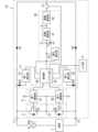
以下、本実施形態の調光装置1について説明する。ただし、以下に説明する構成は、本発明の一例に過ぎず、本発明は、下記実施形態に限定されることはなく、この実施形態以外であっても、本発明に係る技術的思想を逸脱しない範囲であれば、設計等に応じて種々の変更が可能である。本実施形態の調光装置1は、図1に示すように、一対の入力端子11,12、双方向スイッチ2、位相検出部3、入力部4、電源部5、制御部6、スイッチ駆動部9、ダイオードD1,D2、及び停止部13を備えている。 (Embodiment 1)
(1.1) Configuration The following describes the
一対の入力端子11,12は、通電時に点灯する負荷7と交流電源8との間に電気的に接続される。双方向スイッチ2は、一対の入力端子11,12間において、双方向の電流の遮断/導通を切り替えるように構成されている。位相検出部3は、交流電源8の交流電圧Vacの位相を検出する。入力部4は、負荷7の光出力の大きさを指定する調光レベルが入力される。電源部5は、一対の入力端子11,12間に電気的に接続され、交流電源8からの供給電力により制御電源を生成する。The pair of
制御部6は、電源部5から制御電源の供給を受けて動作する。位相検出部3からの検出信号に基づいて、交流電圧Vacの半周期の始点から第1時間が経過する第1時点まで双方向スイッチ2がオフ状態となるように、制御部6が双方向スイッチ2を制御する。第1時点から調光レベルに応じた第2時間が経過する第2時点までは双方向スイッチ2がオン状態となるように、制御部6が双方向スイッチ2を制御する。また、第2時点から半周期の終点までは双方向スイッチ2がオフ状態となるように、制御部6が双方向スイッチ2を制御する。The
ここで「時点Aから」という表現は、時点Aを含む意味とする。例えば「第1時点から」は、第1時点を含む意味である。一方、「時点Aまで」という表現は、時点Aは含まず、時点Aの直前までを意味する。例えば「第1時点まで」は、第1時点は含まず、第1時点の直前までを意味する。また、ここでいう「入力端子」は、電線等を接続するための部品(端子)として実体を有しなくてもよく、例えば電子部品のリードや、回路基板に含まれる導体の一部であってもよい。The expression "from time A" here means to include time A. For example, "from the first time point" means to include the first time point. On the other hand, the expression "until time A" means to the time just before time A, not including time A. For example, "until the first time point" means to the time just before the first time, not including the first time point. Also, the "input terminal" here does not have to have a physical form as a part (terminal) for connecting an electric wire or the like, and may be, for example, a lead of an electronic component or a part of a conductor included in a circuit board.
調光装置1は、2線式の調光装置であって、交流電源8に対して負荷7と電気的に直列に接続された状態で使用される。負荷7は通電時に点灯する。負荷7は、光源としてのLED素子と、LED素子を点灯させる点灯回路と、を備えている。交流電源8は、例えば単相100〔V〕、60〔Hz〕の商用電源である。調光装置1は、一例として壁スイッチ等に適用可能である。The
双方向スイッチ2は、例えば、入力端子11,12間に電気的に直列に接続された第1のスイッチ素子Q1及び第2のスイッチ素子Q2の2個の素子からなる。例えば、スイッチ素子Q1,Q2の各々は、エンハンスメント形のnチャネルMOSFET(Metal-Oxide-Semiconductor Field Effect Transistor)からなる半導体スイッチ素子である。The
スイッチ素子Q1,Q2は、入力端子11,12間において、いわゆる逆直列に接続されている。つまり、スイッチ素子Q1,Q2はソース同士が互いに接続されている。スイッチ素子Q1のドレインは入力端子11に接続され、スイッチ素子Q2のドレインは入力端子12に接続されている。両スイッチ素子Q1,Q2のソースは、電源部5のグランドに接続されている。電源部5のグランドは、調光装置1の内部回路にとって基準電位となる。The switch elements Q1 and Q2 are connected in what is called an anti-series configuration between the
双方向スイッチ2は、スイッチ素子Q1,Q2のオン、オフの組み合わせにより、4つの状態を切替可能である。4つの状態には、両スイッチ素子Q1,Q2が共にオフである双方向オフ状態と、両スイッチ素子Q1,Q2が共にオンである双方向オン状態と、スイッチ素子Q1,Q2の一方のみがオンである2種類の一方向オン状態とがある。一方向オン状態では、スイッチ素子Q1,Q2のうち、オンの方のスイッチ素子から、オフの方のスイッチ素子の寄生ダイオードを通して一対の入力端子11,12間が一方向に導通することになる。例えば、スイッチ素子Q1がオン、スイッチ素子Q2がオフの状態では、入力端子11から入力端子12に向けて電流を流す第1の一方向オン状態となる。また、スイッチ素子Q2がオン、スイッチ素子Q1がオフの状態では、入力端子12から入力端子11に向けて電流を流す第2の一方向オン状態となる。そのため、入力端子11,12間に交流電源8から交流電圧Vacが印加される場合、交流電圧Vacの正極性、つまり入力端子11が正極の半周期においては、第1の一方向オン状態が「順方向オン状態」、第2の一方向オン状態が「逆方向オン状態」となる。一方、交流電圧Vacの負極性、つまり入力端子12が正極の半周期においては、第2の一方向オン状態が「順方向オン状態」、第1の一方向オン状態が「逆方向オン状態」となる。The
ここで、双方向スイッチ2は、「双方向オン状態」及び「順方向オン状態」の両状態がオン状態であり、「双方向オフ状態」及び「逆方向オン状態」の両状態がオフ状態である。Here, the
位相検出部3は、入力端子11,12間に印加される交流電圧Vacの位相を検出する。ここでいう「位相」には、交流電圧Vacのゼロクロス点、交流電圧Vacの極性(正極性、負極性)を含んでいる。位相検出部3は、交流電圧Vacのゼロクロス点を検出すると検出信号を制御部6に出力するように構成されている。位相検出部3は、ダイオードD31と、第1検出部31と、ダイオードD32と、第2検出部32と、を有している。第1検出部31は、ダイオードD31を介して入力端子11に電気的に接続されている。第2検出部32は、ダイオードD32を介して入力端子12に電気的に接続されている。第1検出部31は、交流電圧Vacが負極性の半周期から正極性の半周期に移行する際のゼロクロス点を検出する。第2検出部32は、交流電圧Vacが正極性の半周期から負極性の半周期に移行する際のゼロクロス点を検出する。The
すなわち、第1検出部31は、入力端子11を正極とする電圧が規定値未満の状態から規定値以上の状態に移行したことを検出すると、ゼロクロス点と判断する。同様に、第2検出部32は、入力端子12を正極とする電圧が規定値未満の状態から規定値以上の状態に移行したことを検出すると、ゼロクロス点と判断する。規定値は0〔V〕付近に設定された値(絶対値)である。例えば、第1検出部31の規定値は、プラス数〔V〕程度であり、第2検出部32の規定値は、マイナス数〔V〕程度である。したがって、第1検出部31及び第2検出部32で検出されるゼロクロス点の検出点は、厳密な意味でのゼロクロス点(0〔V〕)から少し時間が遅れる。That is, when the
入力部4は、ユーザによって操作される操作部から、調光レベルを表す信号を受け付け、制御部6に調光信号として出力する。入力部4は、調光信号を出力するのに際して、受け付けた信号を加工してもよいし、しなくてもよい。調光信号とは、負荷7の光出力の大きさを指定する数値等であって、負荷7を消灯状態とする「OFFレベル」を含む場合もある。操作部は、ユーザの操作を受けて入力部4に調光レベルを表す信号を出力する構成であればよく、例えば可変抵抗器やロータリスイッチ、タッチパネル、リモートコントローラ、あるいはスマートフォン等の通信端末などである。The input unit 4 receives a signal representing a dimming level from an operation unit operated by a user, and outputs the signal as a dimming signal to the
制御部6は、位相検出部3からの検出信号及び入力部4からの調光信号に基づいて双方向スイッチ2を制御する。制御部6は、スイッチ素子Q1,Q2の各々を別々に制御する。具体的には、制御部6は、第1制御信号にてスイッチ素子Q1を制御し、第2制御信号にてスイッチ素子Q2を制御する。The
制御部6は、例えばマイクロコンピュータを主構成として備えている。マイクロコンピュータは、マイクロコンピュータのメモリに記録されているプログラムをCPU(Central Processing Unit)で実行することにより、制御部6としての機能を実現する。プログラムは、予めマイクロコンピュータのメモリに記録されていてもよいし、メモリカードのような記録媒体に記録されて提供されたり、電気通信回線を通して提供されたりしてもよい。言い換えれば、上記プログラムは、コンピュータ(ここではマイクロコンピュータ)を、制御部6として機能させるためのプログラムである。The
スイッチ駆動部9は、スイッチ素子Q1を駆動(オン/オフ制御)する第1駆動部91と、スイッチ素子Q2を駆動(オン/オフ制御)する第2駆動部92と、を有している。第1駆動部91は、制御部6から第1制御信号を受けて、スイッチ素子Q1にゲート電圧を印加する。これにより、第1駆動部91はスイッチ素子Q1をオン/オフ制御する。同様に、第2駆動部92は、制御部6から第2制御信号を受けて、スイッチ素子Q2にゲート電圧を印加する。これにより、第2駆動部92はスイッチ素子Q2をオン/オフ制御する。第1駆動部91は、スイッチ素子Q1のソースの電位を基準にしてゲート電圧を生成する。第2駆動部92も同様である。The
電源部5は、制御電源を生成する制御電源部51と、駆動電源を生成する駆動電源部52と、容量性素子(コンデンサ)C1と、を有している。制御電源は、制御部6の動作用の電源である。駆動電源は、スイッチ駆動部9の駆動用の電源である。容量性素子C1は、制御電源部51の出力端子に電気的に接続されており、制御電源部51の出力電流により充電される。The
電源部5は、ダイオードD1を介して入力端子11に電気的に接続され、ダイオードD2を介して入力端子12に電気的に接続されている。これにより、一対のダイオードD1,D2と、スイッチ素子Q1,Q2の各々の寄生ダイオードとで構成されるダイオードブリッジにて、入力端子11,12間に印加される交流電圧Vacが全波整流されて、電源部5に供給される。駆動電源部52は、全波整流された交流電圧Vacを平滑化し、駆動電源を生成する。駆動電源部52は、スイッチ駆動部9及び制御電源部51に、駆動電源を供給する。駆動電源は、例えば10〔V〕である。制御電源部51は、駆動電源部52から供給された駆動電源を降圧して制御電源を生成し、容量性素子C1に出力する。制御電源は、例えば3〔V〕である。制御電源部51は、駆動電源部52を介さず、全波整流された交流電圧Vacから直接制御電源を生成してもよい。つまり、電源部5は、交流電源8からの供給電力により制御電源及び駆動電源を生成する。The
停止部13は、停止期間において、電源部5での制御電源の生成を停止させる。本実施形態では、停止部13は、電源部5を電気的に遮断したり、電源部5に含まれる半導体スイッチ素子を制御したりすることにより、電源部5での制御電源の生成を停止させる。図1の例では、停止部13は電源部5と直列回路を構成し、停止部13と電源部5との直列回路は、一対の入力端子11,12間において双方向スイッチ2と、電気的に並列に接続される。詳しくは、「(1.2.2)調光動作」の欄で説明するが、停止期間は、少なくとも双方向スイッチ2が双方向オフ状態の期間を除いて設定された期間である。具体的には、停止部13は、一対のダイオードD1,D2の接続点と、電源部5との間に電気的に接続されたスイッチであって、制御部6からの遮断信号を受けてオフし、入力端子11,12から電源部5を電気的に切り離す。The
また、本実施形態の調光装置1はマスク部61を備えている。マスク部61は、位相検出部3から検出信号を受信すると、一定長さのマスク時間に亘って検出信号を無効にする。本実施形態では、マスク部61は、制御部6の一機能として、制御部6と一体に設けられている。詳しくは、「(1.2.2)調光動作」の欄で説明するが、マスク部61は、マスク時間には、位相検出部3からの検出信号を無効にすることにより、位相検出部3でのゼロクロス点の誤検出の影響を制御部6は受けにくくなる。マスク部61は、第1検出部31及び第2検出部32の各々について別々に検出信号を無効にするのが好ましい。The dimming
負荷7の点灯回路は、調光装置1で位相制御された交流電圧Vacの波形から調光レベルを読み取り、LED素子の光出力の大きさを変化させる。ここで、点灯回路は、一例としてブリーダ回路などの電流確保用の回路を有している。そのため、調光装置1の双方向スイッチ2が非導通となる期間においても、負荷7に電流を流すことが可能である。The lighting circuit of the
(1.2)動作
(1.2.1)起動動作
まず、本実施形態の調光装置1の通電開始時の起動動作について説明する。 (1.2) Operation (1.2.1) Start-up Operation First, a start-up operation at the start of energization of the
上述した構成の調光装置1によれば、入力端子11,12間に負荷7を介して交流電源8が接続されると、交流電源8から入力端子11,12間に印加される交流電圧Vacが整流されて駆動電源部52に供給される。駆動電源部52で生成された駆動電源はスイッチ駆動部9に供給され、かつ制御電源部51に供給される。制御電源部51で生成された制御電源が制御部6に供給されると、制御部6が起動する。According to the
制御部6が起動すると、制御部6は、位相検出部3の検出信号を基に交流電源8の周波数の判定を行う。そして、制御部6は、判定した周波数に応じて、予めメモリに記憶されている数値テーブルを参照し、各種の時間などのパラメータ(例えば後述するマスク時間や停止期間)の設定を行う。ここで、入力部4に入力された調光レベルが「OFFレベル」であれば、制御部6は、双方向スイッチ2を双方向オフ状態に維持することで、一対の入力端子11,12間のインピーダンスをハイインピーダンス状態に維持する。これにより、負荷7は消灯状態を維持する。When the
(1.2.2)調光動作
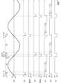
次に、本実施形態の調光装置1の調光動作について、図2を参照して説明する。図2では、交流電圧「Vac」、第1検出信号「ZC1」、第1マスク処理「MASK1」、第2検出信号「ZC2」、第2マスク処理「MASK2」、第1制御信号「Sb1」、第2制御信号「Sb2」、及び遮断信号「Ss1」を示している。ここで、第1検出信号ZC1は第1検出部31による検出信号、第2検出信号ZC2は第2検出部32による検出信号である。第1マスク処理MASK1はマスク部61による第1検出信号ZC1に対するマスク処理(無効化処理)、第2マスク処理MASK2はマスク部61による第2検出信号ZC2に対するマスク処理である。ここでは、第1検出信号ZC1が「H」レベルから「L」レベルに変化することをもって、第1検出信号ZC1が発生したこととする。また、第2検出信号ZC2が「H」レベルから「L」レベルに変化することをもって、第2検出信号ZC2が発生したこととする。つまり、第1検出信号ZC1及び第2検出信号ZC2は、ゼロクロス点の検出時に「H」レベルから「L」レベルに変化する信号である。 (1.2.2) Dimming Operation Next, the dimming operation of the
まず、交流電圧Vacが正極性の半周期における調光装置1の動作について説明する。調光装置1は、位相制御の基準となる交流電圧Vacのゼロクロス点を位相検出部3で検出する。交流電圧Vacが負極性の半周期から正極性の半周期に移行する際には、交流電圧Vacが正極性の規定値「Vzc」に達すると、第1検出部31が第1検出信号ZC1を出力する。第1検出信号ZC1を受けると、制御部6は、第1制御信号Sb1及び第2制御信号Sb2を「OFF」信号にする。First, the operation of the
これにより、半周期の始点(ゼロクロス点)t0から第1時間が経過する第1時点t1までの第一の期間T1では、スイッチ素子Q1,Q2がいずれもオフになり、双方向スイッチ2が双方向オフ状態となる。本実施形態では、第1検出信号ZC1の発生時点を「検出点」とし、半周期の始点(ゼロクロス点)t0から検出点までの期間と、検出点から一定時間(例えば300〔μs〕)が経過するまでの期間の合計を、第一の期間T1とする。つまり、本実施形態では、検出点以降だけでなく、半周期の始点(ゼロクロス点)t0から検出点までの期間にも、制御部6は、双方向スイッチ2を双方向オフ状態に制御する。ここで、交流電圧Vacの周波数が一定であれば、半周期の始点(ゼロクロス点)t0から検出点までの時間は一定長さの時間であるため、本実施形態における第1時間(半周期の始点t0から第1時点t1までの時間)は一定長さの時間である。As a result, in the first period T1 from the start point (zero crossing point) t0 of the half cycle to the first time point t1 at which the first time has elapsed, both switch elements Q1 and Q2 are turned off, and the
検出点から一定時間(例えば300〔μs〕)が経過した時点、つまり第1時点t1において、制御部6は、第1制御信号Sb1及び第2制御信号Sb2を「ON」信号にする。When a certain time (e.g., 300 μs) has elapsed from the detection point, that is, at the first time point t1, the
第2時点t2は、第1時点t1から調光信号に応じた第2時間が経過した時点である。第2時点t2においては、制御部6は、第2制御信号Sb2を「ON」信号に維持したまま、第1制御信号Sb1を「OFF」信号にする。これにより、第1時点t1から第2時点t2までの第二の期間T2には、スイッチ素子Q1,Q2がいずれもオンになり、双方向スイッチ2が双方向オン状態となる。そのため、第二の期間T2には、交流電源8から双方向スイッチ2を介して負荷7へ電力が供給され、負荷7が点灯する。The second time point t2 is the time point when a second time corresponding to the dimming signal has elapsed from the first time point t1. At the second time point t2, the
第3時点t3は、半周期の終点(ゼロクロス点)t4よりも一定時間(例えば300〔μs〕)だけ手前の時点である。第3時点t3においては、制御部6は、第1制御信号Sb1及び第2制御信号Sb2を「OFF」信号にする。これにより、第2時点t2から第3時点t3までの第三の期間T3には、スイッチ素子Q1,Q2のうちスイッチ素子Q1のみがオフし、双方向スイッチ2が逆方向オン状態(つまり、オフ状態)となる。そのため、第三の期間T3には、交流電源8から負荷7への電力が断たれる。The third time point t3 is a fixed time (e.g., 300 μs) before the end point (zero cross point) t4 of the half cycle. At the third time point t3, the
第3時点t3から半周期の終点(ゼロクロス点)t4までの第四の期間T4には、スイッチ素子Q1,Q2がいずれもオフになり、双方向スイッチ2が双方向オフ状態となる。During the fourth period T4 from the third time point t3 to the end point (zero crossing point) t4 of the half cycle, both switch elements Q1 and Q2 are turned off, and the
また、交流電圧Vacが負極性の半周期における調光装置1の動作は、正極性の半周期と基本的に同様の動作となる。In addition, the operation of the
負極性の半周期において、半周期の始点(ゼロクロス点)t0(t4)から第1時間が経過する第1時点t1までの期間を第一の期間T1とする。本実施形態では、第2検出信号ZC2の発生時点を「検出点」とし、半周期の始点(ゼロクロス点)t0(t4)から検出点までの期間と、検出点から一定時間(例えば300〔μs〕)が経過するまでの期間の合計を、第一の期間T1とする。また、第2時点t2は、第1時点t1から調光信号に応じた第2時間が経過した時点であり、第3時点t3は、半周期の終点(ゼロクロス点)t4(t0)よりも一定時間(例えば300〔μs〕)だけ手前の時間である。すなわち、交流電圧Vacが負極性の規定値「-Vzc」に達すると、第2検出部32が第2検出信号ZC2を出力する。第2検出信号ZC2を受けると、制御部6は、第1制御信号Sb1及び第2制御信号Sb2を「OFF」信号にする。これにより、第一の期間T1には双方向スイッチ2が双方向オフ状態となる。そして、第1時点t1において、制御部6は、第1制御信号Sb1及び第2制御信号Sb2を「ON」信号にする。In the negative half cycle, the period from the start point (zero crossing point) t0 (t4) of the half cycle to the first time point t1 at which the first time has elapsed is defined as the first period T1. In this embodiment, the time point at which the second detection signal ZC2 is generated is defined as the "detection point", and the sum of the period from the start point (zero crossing point) t0 (t4) of the half cycle to the detection point and the period from the detection point until a certain time (for example, 300 μs) has elapsed is defined as the first period T1. The second time point t2 is the time at which the second time corresponding to the dimming signal has elapsed from the first time point t1, and the third time point t3 is a certain time (for example, 300 μs) before the end point (zero crossing point) t4 (t0) of the half cycle. That is, when the AC voltage Vac reaches the negative polarity specified value "-Vzc", the
第2時点t2においては、制御部6は、第1制御信号Sb1を「ON」信号に維持したまま、第2制御信号Sb2を「OFF」信号にする。これにより、第1時点t1から第2時点t2までの第二の期間T2には、スイッチ素子Q1,Q2がいずれもオンになり、双方向スイッチ2が双方向オン状態となる。そのため、第二の期間T2には、交流電源8から双方向スイッチ2を介して負荷7へ電力が供給され、負荷7が点灯する。At the second time point t2, the
第3時点t3においては、制御部6は、第1制御信号Sb1及び第2制御信号Sb2を「OFF」信号にする。これにより、第2時点t2から第3時点t3までの第三の期間T3には、スイッチ素子Q1,Q2のうちスイッチ素子Q2のみがオフし、双方向スイッチ2が逆方向オン状態(つまり、オフ状態)となる。そのため、第三の期間T3には、交流電源8から負荷7への電力が断たれる。At the third time point t3, the
本実施形態の調光装置1は、以上説明した正極性の半周期の動作と負極性の半周期の動作とを交流電圧Vacの半周期ごとに交互に繰り返すことで、負荷7の調光を行う。半周期の始点(ゼロクロス点)t0から第1時点t1までの期間には双方向スイッチはオフ状態にあり、また、第2時点t2から半周期の終点(ゼロクロス点)t4までの期間には双方向スイッチはオフ状態にある。したがって、連続する2つの半周期に着目すると、1つ目の半周期の第2時点t2から、次の半周期(つまり2つ目の半周期)の第1時点t1までは、双方向スイッチはオフ状態となる。The dimming
ここで、第1時点t1から第2時点t2までの時間(第2時間)は、入力部4に入力された調光レベルに応じた時間であるので、半周期において入力端子11,12間が導通する時間は、調光レベルに従って規定されることになる。すなわち、負荷7の光出力を小さくする場合には第2時間は短く、負荷7の光出力を大きくする場合には第2時間は長く規定される。そのため、入力部4に入力される調光レベルに応じて、負荷7の光出力の大きさを変えることが可能である。また、交流電圧Vacのゼロクロス点の前後には、それぞれ双方向スイッチ2が双方向オフ状態となる期間(第一の期間T1、第四の期間T4)があるので、調光装置1は、この期間を用いて交流電源8から電源部5への電力供給を確保できる。本実施形態の場合、第一の期間T1及び第四の期間T4の少なくとも一方で交流電源8から電源部5への電力供給を確保することができる。なお、ユーザが操作部を負荷7の光出力を最大にするように操作した場合に、第一の期間T1及び第四の期間T4の確保を優先し、第二の期間T2については光出力を最大にする長さよりも短い期間に制御するようにしてもよい。Here, the time from the first time t1 to the second time t2 (the second time) corresponds to the dimming level input to the input unit 4, so the time during which the
ところで、本実施形態の調光装置1は、マスク部61を備え、ゼロクロス点の検出信号を受信後、一定長さのマスク時間に亘って以降のゼロクロス点の検出信号を無効にするマスク処理を行っている。すなわち、マスク部61は、第1検出部31からの第1検出信号ZC1を受けた後、第1マスク処理MASK1を「ON」にし、マスク時間が経過するまで第1検出信号ZC1を無効にする。同様に、マスク部61は、第2検出部32からの第2検出信号ZC2を受けた後、第2マスク処理MASK2を「ON」にし、マスク時間が経過するまで第2検出信号ZC2を無効にする。マスク時間の長さは、交流電圧Vacの半周期を基準にして設定されている。ここでは一例として、半周期の2倍(つまり1周期)よりもやや短い時間をマスク時間とする。図2では、無効化された期間の第1検出信号ZC1及び第2検出信号ZC2を破線で表している。The dimming
これにより、一旦ゼロクロス点が検出されると、次のゼロクロス点の付近まではマスク処理が施される。例えばゼロクロス点が検出されてから1/4周期の時点でノイズの影響によりゼロクロス点が誤検出されるような場合であっても、誤検出にて発生した検出信号はマスク処理によって無効化されることになる。したがって、位相検出部3でのゼロクロス点の誤検出の影響を制御部6が受けにくくなる。As a result, once a zero-crossing point is detected, masking is performed up to the vicinity of the next zero-crossing point. For example, even if a zero-crossing point is erroneously detected due to
また、本実施形態の調光装置1は、遮断信号Ss1にて停止部13を制御する。停止期間において、停止部13は、電源部5を電気的に遮断したり、電源部5に含まれる半導体スイッチ素子を制御したりすることにより、電源部5での制御電源の生成を停止させている。すなわち、制御部6は、停止期間に遮断信号Ss1を「OFF」信号にして停止部13をオフすることにより、入力端子11,12から電源部5を電気的に切り離す。停止期間は、少なくとも双方向スイッチ2が双方向オフ状態の期間(第一の期間T1、第四の期間T4)を除いて設定された期間である。つまり、停止期間は、双方向スイッチ2が双方向オン状態となる第二の期間T2、及び双方向スイッチ2が一方向オン状態(逆方向オン状態)となる第三の期間T3内に設定される。ここでは一例として、第1時点t1と第2時点t2との間に設定された時点を始点とし第3時点t3を終点とするように停止期間が設定されている。すなわち、停止期間は、交流電源8から負荷7へ電力供給される可能性がある期間内に設定されている。In addition, the dimming
これにより、調光装置1は、停止期間においては、入力端子11,12から電源部5を切り離した分だけ、入力端子11,12間のインピーダンスを高く維持できる。つまり、調光装置1は、双方向スイッチ2が双方向オフ状態の期間には交流電源8から電源部5への電力供給を行い、電源部5への電力供給を行わない期間(停止期間)には、入力端子11,12間のインピーダンスを高く維持することができる。例えば、双方向スイッチ2が逆方向オン状態となる第三の期間T3に、入力端子11,12間のインピーダンスが高く維持されることで、漏れ電流によって負荷7へ電力が供給されてしまうことを防止できる。これにより、調光レベルの細かな変化に追従して負荷7の光出力の大きさが変化可能になり、負荷7の応答性が向上する。As a result, the dimming
(1.3)実施形態1に係る調光装置の要約
以上説明したように、本実施形態に係る調光装置1は、双方向スイッチ2と、位相検出部3と、電源部5と、制御部6と、を具備している。 (1.3) Summary of the dimmer according to the first embodiment As described above, the
双方向スイッチ2は、交流電源8に対して負荷7と直列に接続され、負荷7に供給する交流電圧Vacを位相制御する。位相検出部3は、交流電源8の交流電圧Vacの位相を検出する。電源部5は、双方向スイッチ2と並列に接続され、交流電源8を所定の制御電源に変換する変換動作を行い、制御電源を蓄積する容量性素子C1を有する。The
制御部6は、電源部5から容量性素子C1を通じて制御電源が供給され、位相検出部3で検出された位相に基づき、交流電圧Vacの毎半周期の期間を第一の期間T1、第二の期間T2、第三の期間T3、及び第四の期間T4に区分する。制御部6は、第一の期間T1及び第四の期間T4では、双方向スイッチ2を非導通制御して負荷7への電力供給を遮断し、電源部5に変換動作を行わせる。制御部6は、第二の期間T2では、双方向スイッチ2を導通制御して負荷7に電力供給し、電源部5に変換動作を停止させる。制御部6は、第三の期間T3では、双方向スイッチ2を非導通制御して負荷7への電力供給を遮断する。The
ここでいう「非導通制御」は、双方向スイッチ2をオフ状態にする制御を意味する。また、「導通制御」は、双方向スイッチ2をオン状態にする制御を意味する。また、「変換動作」は、電源部5において、交流電源8を所定の制御電源に変換する動作、つまり交流電源8からの供給電力により制御電源を生成する動作を意味する。The term "non-conductive control" here refers to control that turns the
また、調光装置1は、電源部5の変換動作の実行/停止を切り替える停止部13を、更に具備していてもよい。この場合、例えば第三の期間(T3)において、制御部6にて双方向スイッチ2を非導通制御して負荷7への電力供給を遮断することに加え、停止部13にて電源部5の変換動作を停止させてもよい。The
(1.4)比較例との対比
以下、本実施形態とは異なる逆位相制御方式を比較例とし、本実施形態の制御方式と比較例の制御方式とを対比した場合の、両者の相違点について図3を参照して説明する。 (1.4) Comparison with Comparative Example Hereinafter, an inverse phase control method different from that of the present embodiment will be used as a comparative example, and the differences between the control method of the present embodiment and the control method of the comparative example will be described with reference to FIG. 3.
ここで示す比較例は、制御部6の動作(双方向スイッチ2の制御方式)が本実施形態とは異なるものの、回路構成については本実施形態と同じであるため、以下、本実施形態と同様の構成要素については共通の符号を付して説明する。図3では、交流電圧「Vac」と、比較例の第1制御信号「Sa1」及び第2制御信号「Sa2」と、本実施形態の第1制御信号「Sb1」及び第2制御信号「Sb2」と、を表している。In the comparative example shown here, the operation of the control unit 6 (the control method of the bidirectional switch 2) is different from that of this embodiment, but the circuit configuration is the same as that of this embodiment, so in the following description, the same components as in this embodiment are denoted by the same reference numerals. Figure 3 shows the AC voltage "Vac", the first control signal "Sa1" and the second control signal "Sa2" of the comparative example, and the first control signal "Sb1" and the second control signal "Sb2" of this embodiment.
比較例の調光装置は、交流電圧Vacと同じ周期で、第1制御信号Sa1と第2制御信号Sa2とを交互に「ON」する。この比較例によれば、スイッチ素子Q1,Q2のうち、交流電圧Vacの高電位側となるスイッチ素子がオンしている期間に、双方向スイッチ2が導通することになる。つまり、比較例では、図3において、交流電圧Vacのゼロクロス点から半周期の途中までの期間Ta1に一対の入力端子11,12間が導通する、いわゆる逆位相制御が実現される。したがって、第1制御信号Sa1及び第2制御信号Sa2と交流電圧Vacとの位相差を調節することで、双方向スイッチ2の導通時間を調節することができる。The dimmer of the comparative example alternately turns on the first control signal Sa1 and the second control signal Sa2 in the same cycle as the AC voltage Vac. According to this comparative example, the
したがって、本実施形態と上記比較例とを対比すると両者は以下の相違点1,2で相違する。Therefore, when comparing this embodiment with the above comparative example, the two differ in the following
〔相違点1〕
図3に〔X〕で示すように、本実施形態では双方向スイッチ2が双方向オン状態となる期間(第二の期間T2)が存在するのに対して、比較例では双方向スイッチ2が双方向オン状態となる期間が存在しない点で相違する。 [Difference 1]
As indicated by [X] in FIG. 3 , the present embodiment differs from the comparative example in that there is a period (second period T2) during which the
つまり、比較例では、双方向スイッチ2が一方向オン状態(順方向オン状態)となることで一対の入力端子11,12間が導通するのに対し、本実施形態では、双方向スイッチ2が双方向オン状態となることで一対の入力端子11,12間が導通する。このように、本実施形態の調光装置1は、一対の入力端子11,12間の導通時、双方向スイッチ2が双方向オン状態になるので、双方向スイッチ2が一方向オン状態である比較例に比べて、双方向スイッチ2での導通損失を小さく抑えることができる。In other words, in the comparative example, the
〔相違点2〕
図3に〔Y〕で示すように、交流電圧Vacのゼロクロス点の前後に、本実施形態では双方向スイッチ2が双方向オフ状態となる期間(第一の期間T1,第四の期間T4)が存在するのに対して、比較例ではこのような期間が存在しない点で相違する。 [Difference 2]
As indicated by [Y] in FIG. 3 , before and after the zero-crossing points of the AC voltage Vac, there are periods (a first period T1 and a fourth period T4) in which the
つまり、比較例では、交流電圧Vacのゼロクロス点から半周期の途中までの期間Ta1には一対の入力端子11,12間が導通するので、交流電源8から電源部5への電力供給の機会を半周期の後半部分でのみ確保することになる。ところが、例えばコンデンサインプット型の点灯回路を採用した負荷7など、負荷7の種類によっては、交流電圧Vacの半周期の後半部分に負荷7に電流が流れない場合がある。そのため、比較例においては、一対の入力端子11,12間が非導通の期間に、電源部5に十分な電流を流すことができず、交流電源8から電源部5への供給電力を十分に確保できない可能性がある。その結果、比較例においては、電源部5から制御部6への制御電源の供給を維持できなくなる可能性がある。In other words, in the comparative example, the pair of
これに対して、本実施形態の調光装置1は、半周期の始点(ゼロクロス点)t0から第1時点t1までの期間(第一の期間T1)においては、双方向スイッチ2を双方向オフ状態とするので、この期間を電源部5への給電に充てることができる。本実施形態の調光装置1は、基本的に逆位相制御を採用しながらも、交流電圧Vacの半周期の前半部分に双方向スイッチ2が非導通となる期間(第一の期間T1)を設けたことで、交流電源8から電源部5への電力供給の機会を半周期の前半部分に確保できる。したがって、本実施形態の調光装置1は、比較例に比べて、より多くの種類の負荷7に対応して電源部5から制御部6への電源供給を維持することが可能である。In contrast, the dimming
また、調光装置1は、第3時点t3から半周期の終点t4までの期間(第四の期間T4)にも、双方向スイッチ2を双方向オフ状態とするので、この期間も電源部5への給電に充てることができる。つまり、調光装置1は、半周期の後半部分にも双方向スイッチ2が非導通となる期間(第四の期間T4)を設けたことで、交流電源8から電源部5への電力供給の機会を半周期の後半部分でも確保できる。The
(1.5)利点
調光装置の制御方式には、逆位相制御方式(トレーリングエッジ方式)の他、交流電圧Vacの半周期の途中からゼロクロス点までの期間に一対の入力端子11,12間が導通する、正位相制御方式(リーディングエッジ方式)がある。逆位相制御方式は、光源としてのLED素子を備えた負荷7に、ゼロクロス点から電力供給を開始するため、電力供給開始時の電流波形歪みを小さく抑えることができる。これにより、調光装置に接続可能な負荷7の数(灯数)が増えたり、うなり音の発生を抑制できたりする利点がある。 (1.5) Advantages The control method of the dimmer is not only the reverse phase control method (trailing edge method), but also the positive phase control method (leading edge method) in which a pair of
本実施形態の調光装置1は、基本的に逆位相制御方式を採用しつつも、交流電圧Vacの半周期の前半部分で交流電源8から電源部5への電力供給の機会を設けている。このため、ゼロクロス点から第1時間が経過した第1時点t1で、負荷7に電力供給を開始するため、上記比較例のような逆位相制御方式よりも電流波形歪みは大きくなる可能性がある。ただし、第1時点t1での交流電圧Vacの絶対値はそれほど大きくは無いため、電流波形歪みの影響は無視できるほど小さい。その一方、制御部6の動作に必要な制御電源が確実に確保でき、安定動作させることができるという利点がある。The
さらに、本実施形態の調光装置1は、第2時点t2から第3時点t3までの期間(第三の期間T3)においては、双方向スイッチ2を逆方向オン状態とするので、位相検出部3の誤検出を低減できる。すなわち、負荷7によっては、負荷7の両端電圧の絶対値が交流電圧Vacの絶対値を上回り、その結果、交流電圧Vacとは逆極性の電圧(以下、「逆極性電圧」という)が一対の入力端子11,12に印加されることがある。例えば比較的容量の大きなバッファコンデンサが設けられている負荷7など、両端電圧が下がりにくい負荷7の場合に、このような逆極性電圧が発生しやすい。逆極性電圧が発生すると、交流電圧Vacのゼロクロス点以外のところで、位相検出部3が誤ってゼロクロス点を検出することがある。調光レベルによって逆極性電圧が発生したり発生しなかったりする負荷7もあり、このような負荷7では、調光レベルが変化するとゼロクロス点が急変することになる。第三の期間T3においては、双方向スイッチ2が逆方向オン状態となることで、このような逆極性電圧の発生が抑制されるので、逆極性電圧に起因した位相検出部3の誤検出を低減することができる。勿論、双方向スイッチ2が逆方向オン状態の期間(第三の期間T3)であっても、一対の入力端子11,12間は非導通であるので、遮断信号を「ON」信号にすることで、この期間を電源部5への給電に充てることができる。Furthermore, in the
調光装置1は、電源部5から制御部6への電源供給を維持できることで、負荷7の点滅や、ちらつきなどの異常動作を防止できる。The
本実施形態での双方向スイッチ2の制御においては、「双方向オン状態」の代わりに「順方向オン状態」に制御することも可能であり、逆に「順方向オン状態」の代わりに「双方向オン状態」に制御することも可能である。また、「双方向オフ状態」の代わりに「逆方向オン状態」に制御することも可能であり、「逆方向オン状態」の代わりに「双方向オフ状態」に制御することも可能である。すなわち、双方向スイッチ2が、オン状態又はオフ状態の状態が変わらなければよい。In controlling the
また、本実施形態のように、双方向スイッチ2は、入力端子11,12間において、双方向の電流を遮断する双方向オフ状態、双方向の電流を通過させる双方向オン状態、及び一方向の電流を通過させる一方向オン状態を切替可能に構成されていることが好ましい。この場合、制御部6は、第2時点t2から第2時点t2と半周期の終点との間の第3時点t3までは、双方向スイッチ2が逆方向オン状態となるように、双方向スイッチ2を制御するように構成されていることが好ましい。「逆方向オン状態」とは、双方向スイッチ2が入力端子11,12のうち交流電源8の低電位側の入力端子から高電位側の入力端子に電流を流す向きの一方向オン状態である。この構成によれば、第2時点t2から第3時点t3までは、逆極性電圧の発生が抑制されるので、逆極性電圧に起因した位相検出部3の誤検出を低減することができる。As in this embodiment, the
また、本実施形態のように、電源部5は容量性素子C1を有することが好ましい。この構成によれば、電源部5は、入力端子11,12間が非導通となる期間に交流電源8から供給される電力を、容量性素子C1に蓄えることができる。したがって、入力端子11,12間が導通する期間でも、電源部5は制御部6の制御電源を確保することができる。ただし、電源部5が容量性素子C1を有することは調光装置1に必須の構成ではなく、容量性素子C1は適宜省略されていてもよい。Furthermore, as in this embodiment, it is preferable that the
また、本実施形態のように、第1時間は一定長さの時間であることが好ましい。この構成によれば、制御部6は、半周期の始点(ゼロクロス点)t0から一定長さの第1時間が経過するまでの期間(第一の期間T1)に、双方向スイッチ2を双方向オフ状態に制御すればよい。したがって、第1時間の長さが変化する場合に比べて、制御部6の処理が簡単になる。Furthermore, as in this embodiment, it is preferable that the first time period is a fixed length of time. According to this configuration, the
制御部6の処理は複雑になるが、正極性の半周期での第一の期間T1と、負極性の半周期での第一の期間T1と、で第1時間の長さを異ならせることも可能である。Although the processing by the
本実施形態のように、位相検出部3は、交流電圧Vacのゼロクロス点を検出すると検出信号を出力するように構成されていることが好ましい。この場合、調光装置1は、位相検出部3から検出信号を受信すると一定長さのマスク時間に亘って検出信号を無効にするマスク部61を、さらに備えることが好ましい。本実施形態でのマスク部61は調光装置1に必須の構成ではなく、マスク部61は適宜省略されていてもよい。As in this embodiment, the
また、本実施形態のように、調光装置1は、停止期間において、電源部5での制御電源の生成を停止させる停止部13を、さらに備えることが好ましい。停止期間は、少なくとも双方向スイッチ2がオフ状態の期間を除いて設定された期間である。本実施形態での停止部13は調光装置1に必須の構成ではなく、停止部13は適宜省略されていてもよい。As in this embodiment, it is preferable that the
また、本実施形態のように、双方向スイッチ2は、一対の入力端子11,12間に電気的に直列に接続されたスイッチ素子Q1,Q2を含むことが好ましい。Furthermore, as in this embodiment, it is preferable that the
(1.6)変形例
(1.6.1)変形例1
実施形態1の変形例1に係る調光装置1Aは、図4に示すように、双方向スイッチ2に相当する部分が、実施形態1の調光装置1と相違する。以下、実施形態1と同様の構成については共通の符号を付して適宜説明を省略する。 (1.6) Modifications (1.6.1)
4, a light control device 1A according to
本変形例では、双方向スイッチ2Aが、ダブルゲート構造のスイッチ素子Q3を含む。スイッチ素子Q3は、例えばGaN(窒化ガリウム)などのワイドバンドギャップの半導体材料を用いたダブルゲート(デュアルゲート)構造の半導体素子である。さらに、双方向スイッチ2Aは、入力端子11,12間において、いわゆる逆直列に接続された一対のダイオードD3,D4を含んでいる。ダイオードD3のカソードは入力端子11に接続され、ダイオードD4のカソードは入力端子12に接続されている。両ダイオードD3,D4のアノードは、電源部5のグランドに電気的に接続されている。本変形例では、一対のダイオードD3,D4が、一対のダイオードD1,D2と共にダイオードブリッジを構成する。In this modification, the
本変形例の構成によれば、双方向スイッチ2Aは、双方向スイッチ2に比較して導通損失のさらなる低減を図ることができる。With the configuration of this modified example,
(1.6.2)変形例2
実施形態1の変形例2に係る調光装置1Bは、図5に示すように、制御部6Bが、1回のゼロクロス点の検出信号に基づいて、半周期以上先の交流電圧Vacのゼロクロス点を推定するように構成されている点で、実施形態1の調光装置1と相違する。調光装置1Bの回路構成は、実施形態1の調光装置1と同じである。以下、実施形態1と同様の構成については共通の符号を付して適宜説明を省略する。 (1.6.2)
A dimming
位相検出部3が、交流電圧Vacのゼロクロス点を検出すると検出信号を出力するように構成されている点は、実施形態1と同様である。As in
本変形例では、制御部6Bは、交流電圧Vacの周波数に基づいて、位相検出部3から検出信号を受ける度に、交流電圧Vacの半周期以上先のゼロクロス点を仮想ゼロクロス点として推定し、仮想ゼロクロス点のタイミングで仮想信号を発生する。具体的には、図6に示すように、制御部6Bは、第1検出信号ZC1を受けた時点から交流電圧Vacの1周期に相当する待機時間Tzcが経過した時点で、第1仮想信号Si1を発生する。同様に、制御部6Bは、第2検出信号ZC2を受けた時点から交流電圧Vacの1周期に相当する待機時間Tzcが経過した時点で、第2仮想信号Si2を発生する。ここで、次の第1検出信号ZC1より先に、第1仮想信号Si1が発生しないよう、待機時間Tzcは、交流電圧Vacの1周期よりやや長く設定されている。また、次の第2検出信号ZC2より先に、第2仮想信号Si2が発生しないよう、待機時間Tzcは、交流電圧Vacの1周期よりやや長く設定されている。In this modification, the
そして、制御部6Bは、第1検出信号ZC1と第1仮想信号Si1との論理和を、双方向スイッチ2の制御のタイミングを決定するトリガ信号とする。同様に、制御部6Bは、第2検出信号ZC2と第2仮想信号Si2との論理和を、双方向スイッチ2の制御のタイミングを決定するトリガ信号とする。したがって、位相検出部3がゼロクロス点を検出し損ねた場合でも、制御部6Bは、位相検出部3からの検出信号の代わりに仮想ゼロクロス点で発生させた仮想信号をトリガ信号にして、双方向スイッチ2の制御のタイミングを決定することができる。The
制御部6Bは、1回のゼロクロス点の検出信号に対して仮想ゼロクロス点を2回以上推定する構成であってもよい。この場合、制御部6Bは、検出信号を受けた時点から待機時間Tzcが経過する度に、仮想信号を発生させる。ここで、1回目の待機時間Tzcは交流電圧Vacの1周期に対して少し長く、2回目以降の待機時間Tzcは交流電圧Vacの1周期と同程度の長さとなるように、待機時間Tzcの長さを変化させてもよい。The
また、仮想信号を発生させる待機時間Tzcは、交流電圧Vacの半周期を基準にして設定されればよく、1周期の他、半周期、半周期の3倍(つまり1.5周期)、半周期の4倍(つまり2周期)以上を基準に設定されてもいてもよい。待機時間Tzcが半周期の奇数倍を基準に設定される場合、制御部6Bは、第1検出信号ZC1に基づいて待機時間Tzcが経過した時点で、第2仮想信号Si2を発生させる。また、この場合、制御部6Bは、第2検出信号ZC2に基づいて待機時間Tzcが経過した時点で、第1仮想信号Si1を発生させる。したがって、制御部6Bは、第1検出信号ZC1及び第2検出信号ZC2のいずれか一方のみから、第1仮想信号Si1及び第2仮想信号Si2を発生させる構成とすることもできる。The waiting time Tzc for generating the virtual signal may be set based on a half cycle of the AC voltage Vac, and may be set based on one cycle, a half cycle, three times a half cycle (i.e., 1.5 cycles), four times a half cycle (i.e., two cycles) or more. When the waiting time Tzc is set based on an odd multiple of a half cycle, the
本変形例の構成によれば、偶発的なノイズ等の影響で位相検出部3にてゼロクロス点を検出できない場合や、瞬間的な交流電圧Vacの低下などでゼロクロス点のずれが発生した場合でも、制御部6Bは、交流電圧Vacの周期に同期して安定した逆位相制御を行う。According to the configuration of this modified example, even if the
(1.6.3)その他の変形例
以下、上述した変形例1,2以外の実施形態1の変形例を列挙する。 (1.6.3) Other Modifications Modifications of the first embodiment other than the first and second modifications described above are listed below.
上述した実施形態1及び変形例1、2の調光装置は、光源としてLED素子を用いた負荷7に限らず、コンデンサインプット型の回路を搭載し、インピーダンスが高く、少ない電流で点灯する光源に適用可能である。この種の光源としては、例えば有機EL(Electroluminescence)素子が挙げられる。また、調光装置は、例えば放電灯など、様々な光源の負荷7に適用可能である。The dimming devices of the above-mentioned
また、スイッチ駆動部9は、調光装置1に必須の構成ではなく、適宜省略されていてもよい。スイッチ駆動部9が省略される場合、制御部6が直接的に双方向スイッチ2を駆動する。The
マスク部61は、一定長さのマスク時間に亘って検出信号を無効にする構成であればよく、制御部6と一体に設けられる構成に限らない。つまり、マスク部61は、例えば位相検出部3と一体に設けられていてもよく、この場合、マスク期間に亘ってマスク部61が位相検出部3の動作を停止することで、検出信号を無効にすることができる。また、マスク部61は、制御部6及び位相検出部3とは、別々に設けられていてもよい。The
さらに、マスク時間は、交流電圧Vacの半周期を基準にして予め設定された時間であればよく、実施形態1で例示したように半周期の2倍(つまり1周期)よりもやや短い時間に限らない。例えば、マスク時間は、半周期よりもやや短い時間、あるいは半周期の3倍(つまり1.5周期)よりもやや短い時間であってもよい。また、マスク時間は、半周期の4倍(つまり2周期)以上を基準に設定されてもいてもよい。Furthermore, the mask time may be a time that is preset based on a half cycle of the AC voltage Vac, and is not limited to a time slightly shorter than twice the half cycle (i.e., one cycle) as exemplified in the first embodiment. For example, the mask time may be a time slightly shorter than the half cycle, or a time slightly shorter than three times the half cycle (i.e., 1.5 cycles). The mask time may also be set based on four times the half cycle (i.e., two cycles) or more.
また、双方向スイッチ2を構成するスイッチ素子Q1,Q2の各々は、エンハンスメント形のnチャネルMOSFETに限らず、例えばIGBT(Insulated Gate Bipolar Transistor)などであってもよい。さらに、双方向スイッチ2において、一方向オン状態を実現するための整流素子(ダイオード)は、スイッチ素子Q1,Q2の寄生ダイオードに限らず、変形例1のように外付けのダイオードであってもよい。ダイオードは、スイッチ素子Q1,Q2の各々と同一パッケージに内蔵されていてもよい。In addition, each of the switch elements Q1 and Q2 constituting the
また、第1時間は一定長さの時間であればよく、その長さは適宜設定可能である。例えば、半周期の始点(ゼロクロス点)t0から検出点までの期間と、検出点から一定の遅延時間が経過するまでの期間の合計が第一の期間T1である場合、遅延時間は300〔μs〕に限らず、0〔μs〕~500〔μs〕の範囲で適宜設定される。The first time period may be a fixed length of time, and the length can be set appropriately. For example, if the first time period T1 is the sum of the period from the start point (zero crossing point) t0 of the half cycle to the detection point and the period from the detection point until a fixed delay time has elapsed, the delay time is not limited to 300 μs, but can be set appropriately in the range of 0 μs to 500 μs.
また、第3時点t3は半周期の終点(ゼロクロス点)t4の手前にあればよく、第3時点t3から半周期の終点t4までの長さは適宜設定可能である。例えば、検出点から第3時点t3までの時間長さが、半周期よりも一定の規定時間だけ短い場合、規定時間は300〔μs〕に限らず、100〔μs〕~500〔μs〕の範囲で適宜設定される。The third point t3 may be located just before the end point (zero cross point) t4 of the half cycle, and the length from the third point t3 to the end point t4 of the half cycle can be set appropriately. For example, if the time length from the detection point to the third point t3 is shorter than the half cycle by a certain specified time, the specified time is not limited to 300 μs, but can be set appropriately in the range of 100 μs to 500 μs.
さらに、停止部13が一対の入力端子11,12と電源部5との間を電気的に遮断する停止期間は、少なくとも双方向スイッチ2が双方向オフ状態の期間(第一の期間T1、第四の期間T4)を除いて設定された期間であればよい。したがって、停止期間は、実施形態1のように、第1時点t1と第2時点t2との間の時点を始点とし第3時点t3を終点とする期間に限らず、例えば停止期間の始点は第1時点t1であってもよく、停止期間の終点が第3時点t3の手前にあってもよい。Furthermore, the stop period during which the
また、停止部13は、停止期間において、電源部5での制御電源の生成を停止させる構成であればよい。そのため、停止部13は、一対の入力端子11,12の少なくとも一方と電源部5との間を電気的に遮断させたり、電源部5に含まれる半導体スイッチ素子を制御したりすることにより、電源部5での制御電源の生成を停止させる構成に限らない。例えば、停止部13は、電源部5の出力(制御電源の出力)を停止することで電源部5の入力インピーダンスを高くし、電源部5での制御電源の生成を停止させる構成であってもよい。The stopping
本実施形態でのダイオードD1,D2は調光装置1に必須の構成ではなく、ダイオードD1,D2は適宜省略されていてもよい。In this embodiment, diodes D1 and D2 are not essential components of the
(実施形態2)
本実施形態の調光装置1Cは、図7に示すように、制御電源の電圧(容量性素子C1の電圧)を検出する電圧検出部53をさらに備える点で、実施形態1の調光装置1と相違する。以下、実施形態1と同様の構成については共通の符号を付して適宜説明を省略する。 (Embodiment 2)
The dimmer 1C of the present embodiment differs from the
本実施形態では、第1時間は一定長さの時間ではなく、交流電圧Vacの半周期の始点(ゼロクロス点)t0から電圧検出部53で検出される電圧(容量性素子C1の電圧)が所定の閾値に達するまでの時間である。すなわち、本実施形態における第1時間は、固定長の時間ではなく、電圧検出部53の検出値に応じて変化する可変長の時間である。In this embodiment, the first time is not a fixed length of time, but is the time from the start point (zero crossing point) t0 of the half cycle of the AC voltage Vac until the voltage detected by the voltage detection unit 53 (the voltage of the capacitive element C1) reaches a predetermined threshold value. In other words, the first time in this embodiment is not a fixed length of time, but a variable length of time that changes depending on the detection value of the
具体的には、電圧検出部53は電源部5Cに設けられている。電圧検出部53は、電源部5Cの容量性素子C1の両端電圧を検出し、検出値を制御部6Cへ出力する。制御部6Cは、位相検出部3から検出信号を受けた後、電圧検出部53の検出値と所定の閾値とを比較し、検出値が閾値に達したことをもって、第1時間が経過した(つまり第1時点t1である)と判断する。ここで、閾値は、少なくとも交流電圧Vacの半周期の終点(ゼロクロス点)t4までの制御部6の動作を確保できる程度に、容量性素子C1が充電されたときの容量性素子C1の両端電圧とする。Specifically, the
以上説明したように、本実施形態の調光装置1Cは、制御電源の電圧を検出する電圧検出部53をさらに備え、第1時間は、半周期の始点から電圧検出部53で検出される電圧が所定の閾値に達するまでの時間である。本実施形態によれば、制御部6は、制御部6の動作に必要な制御電源が確保できる程度に容量性素子C1が充電された時点で、双方向スイッチ2を双方向オン状態とすることができる。したがって、本実施形態の調光装置1Cは、制御部6の動作に必要な制御電源を確実に確保しつつ、交流電圧Vacの半周期の始点(ゼロクロス点)t0から入力端子11,12間が導通するまでの時間を極力短くすることができる。容量性素子C1は寄生容量でもよく、その場合には、別個の容量性素子は無い構成となる。As described above, the dimming
その他の構成及び機能は実施形態1と同様である。本実施形態の構成は、実施形態1(変形例を含む)で説明した各構成と組み合わせて適用可能である。The other configurations and functions are the same as those of the first embodiment. The configuration of this embodiment can be applied in combination with each of the configurations described in the first embodiment (including the modified examples).
(その他の実施形態)
上述の実施形態1(変形例を含む)及び実施形態2では、交流電圧Vacの半周期の始点(ゼロクロス点)t0の前後(第一の期間T1、第四の期間T4)に亘って、交流電源8から電源部5への電力供給を確保しているが、これに限られない。 Other Embodiments
In the above-described first embodiment (including the modified example) and second embodiment, the power supply from the
交流電圧Vacの半周期の始点(ゼロクロス点)t0の後(第一の期間T1)のみ、一定時間の間、交流電源8から電源部5への電力供給を確保してもよい。また、交流電圧Vacの半周期の始点(ゼロクロス点)t0の前(第四の期間T4)のみ、一定時間の間、交流電源8から電源部5への電力供給を確保してもよい。この場合においても、交流電源8から電源部5への電力供給の確保を優先して第一の期間T1または第四の期間T4が設定されるため、入力部4に入力された調光レベルに応じて負荷7へ電力を供給する第二の期間T2が設定されない場合がある。例えば、ユーザが操作部を負荷7の光出力を最大にするように操作する場合である。Power supply from the
上記一定時間を、交流電源8から電源部5への電力供給を十分に行えるように設定することで、電流波形歪みを抑制しつつ、制御部6を安定動作させることができる。By setting the above-mentioned certain time so that sufficient power can be supplied from the
1,1A,1B,1C 調光装置
2,2A 双方向スイッチ(開閉部)
3 位相検出部
4 入力部(設定部)
5,5C 電源部
6,6B,6C 制御部
7 負荷
8 交流電源
11 入力端子(端子)
12 入力端子(端子)
13 停止部
53 電圧検出部
61 マスク部
C1 容量性素子
Q1 スイッチ素子
Q2 スイッチ素子
Q3 スイッチ素子
t0 半周期の始点(ゼロクロス点)
t1 第1時点
t2 第2時点
t3 第3時点
t4 半周期の終点(ゼロクロス点)
Vac 交流電圧
ZC1 第1検出信号
ZC2 第2検出信号 1, 1A, 1B,
3 Phase detection section 4 Input section (setting section)
5, 5C
12 Input terminal (terminal)
13 Stopping
t1: First time point t2: Second time point t3: Third time point t4: End point of half cycle (zero crossing point)
Vac AC voltage ZC1 First detection signal ZC2 Second detection signal
Claims (4)
Translated fromJapanese前記一対の入力端子間において、双方向の電流の遮断と通過とを切り替え可能であり、制御可能な2つの半導体スイッチを備える双方向スイッチと、
調光レベルが入力される入力部と、
前記調光レベルに応じて前記双方向スイッチを制御する制御部と、
前記交流電源から電力供給され前記制御部の電源を生成する制御電源部と、を備え、
前記制御部は、
前記交流電源の交流電圧の半周期の区間において、前記調光レベルに応じて前記2つの半導体スイッチの両方の制御信号を第一の信号として前記双方向スイッチをオフ状態に制御し、
前記双方向スイッチを前記オフ状態に制御した後、前記2つの半導体スイッチの両方の制御信号を第二の信号として前記双方向スイッチをオン状態に制御し、
前記双方向スイッチが前記オフ状態で、前記交流電源から前記制御電源部へ電力を供給するように制御する、
調光装置。 A pair of input terminals electrically connected between the load and the AC power source;
a bidirectional switch including two controllable semiconductor switches that can switch between blocking and passing a bidirectional current between the pair of input terminals;
an input section for inputting a dimming level;
a control unit that controls the bidirectional switch in response to the dimming level;
a control power supply unit that receives power from the AC power supply and generates power for the control unit;
The control unit is
during a half cycle of the AC voltageof the AC power supply , controlling the bidirectional switch to an off state by using both control signals of the two semiconductor switches as a first signal in response to the dimming level;
After controlling the bidirectional switch to the off state, controlling the bidirectional switch to an on state by using both control signals of the two semiconductor switches as second signals;
When the bidirectional switch is in the off state, control is performed so that power is supplied from the AC power supply to the control power supply unit.
Dimmer.
請求項1に記載の調光装置。 the control unit controls the bidirectional switch to be in the on state so as to stop the supply of power from the AC power source to the control power source unit.
The light control device according to claim 1 .
前記制御部は、前記双方向スイッチが前記オフ状態では、前記交流電源から前記制御電源部へ電力を供給するように前記開閉部を制御する、
請求項1又は2に記載の調光装置。 an opening/closing unit connected between the pair of input terminals and the control power supply unit and capable of supplying or cutting off power from the AC power supply to the control power supply unit;
the control unit controls the opening/closing unit to supply power from the AC power source to the control power source unit when the bidirectional switch is in the off state.
The light control device according to claim 1 or 2.
前記制御部は、前記双方向スイッチが前記オン状態では、前記交流電源から前記制御電源部への電力の供給を遮断するように前記開閉部を制御する、
請求項1~3のいずれか1項に記載の調光装置。 an opening/closing unit connected between the pair of input terminals and the control power supply unit and capable of supplying or cutting off power from the AC power supply to the control power supply unit;
the control unit controls the opening/closing unit to cut off the supply of power from the AC power source to the control power source unit when the bidirectional switch is in the on state.
The light control device according to any one of claims 1 to 3.
Applications Claiming Priority (5)
| Application Number | Priority Date | Filing Date | Title |
|---|---|---|---|
| JP2015116179 | 2015-06-08 | ||
| JP2015116179 | 2015-06-08 | ||
| JP2020084810AJP6876949B2 (en) | 2015-06-08 | 2020-05-13 | Dimmer |
| JP2021064317AJP7149635B2 (en) | 2015-06-08 | 2021-04-05 | dimmer |
| JP2022146609AJP7336714B2 (en) | 2015-06-08 | 2022-09-14 | dimmer |
Related Parent Applications (1)
| Application Number | Title | Priority Date | Filing Date |
|---|---|---|---|
| JP2022146609ADivisionJP7336714B2 (en) | 2015-06-08 | 2022-09-14 | dimmer |
Publications (2)
| Publication Number | Publication Date |
|---|---|
| JP2023133531A JP2023133531A (en) | 2023-09-22 |
| JP7611536B2true JP7611536B2 (en) | 2025-01-10 |
Family
ID=57503784
Family Applications (6)
| Application Number | Title | Priority Date | Filing Date |
|---|---|---|---|
| JP2017513826AActiveJP6218101B2 (en) | 2015-06-08 | 2016-05-30 | Light control device |
| JP2017174337AActiveJP6712767B2 (en) | 2015-06-08 | 2017-09-11 | Dimmer |
| JP2020084810AActiveJP6876949B2 (en) | 2015-06-08 | 2020-05-13 | Dimmer |
| JP2021064317AActiveJP7149635B2 (en) | 2015-06-08 | 2021-04-05 | dimmer |
| JP2022146609AActiveJP7336714B2 (en) | 2015-06-08 | 2022-09-14 | dimmer |
| JP2023126703AActiveJP7611536B2 (en) | 2015-06-08 | 2023-08-03 | Light control device |
Family Applications Before (5)
| Application Number | Title | Priority Date | Filing Date |
|---|---|---|---|
| JP2017513826AActiveJP6218101B2 (en) | 2015-06-08 | 2016-05-30 | Light control device |
| JP2017174337AActiveJP6712767B2 (en) | 2015-06-08 | 2017-09-11 | Dimmer |
| JP2020084810AActiveJP6876949B2 (en) | 2015-06-08 | 2020-05-13 | Dimmer |
| JP2021064317AActiveJP7149635B2 (en) | 2015-06-08 | 2021-04-05 | dimmer |
| JP2022146609AActiveJP7336714B2 (en) | 2015-06-08 | 2022-09-14 | dimmer |
Country Status (8)
| Country | Link |
|---|---|
| US (3) | US10306732B2 (en) |
| EP (1) | EP3307026B1 (en) |
| JP (6) | JP6218101B2 (en) |
| KR (1) | KR102075896B1 (en) |
| CN (2) | CN107683631B (en) |
| ES (1) | ES2849803T3 (en) |
| TW (1) | TWI620466B (en) |
| WO (1) | WO2016199368A1 (en) |
Families Citing this family (25)
| Publication number | Priority date | Publication date | Assignee | Title |
|---|---|---|---|---|
| CN103024994B (en)* | 2012-11-12 | 2016-06-01 | 昂宝电子(上海)有限公司 | Use dimming control system and the method for TRIAC dimmer |
| CN103957634B (en) | 2014-04-25 | 2017-07-07 | 广州昂宝电子有限公司 | Lighting system and control method thereof |
| EP3307026B1 (en) | 2015-06-08 | 2020-11-18 | Panasonic Intellectual Property Management Co., Ltd. | Dimmer |
| JP6481943B2 (en) | 2015-09-10 | 2019-03-13 | パナソニックIpマネジメント株式会社 | Light control device |
| JP6867780B2 (en)* | 2016-10-28 | 2021-05-12 | 矢崎総業株式会社 | Semiconductor switch controller |
| JP6830205B2 (en)* | 2016-12-27 | 2021-02-17 | パナソニックIpマネジメント株式会社 | Load control device |
| JP6830204B2 (en)* | 2016-12-27 | 2021-02-17 | パナソニックIpマネジメント株式会社 | Load control device |
| CN107645804A (en) | 2017-07-10 | 2018-01-30 | 昂宝电子(上海)有限公司 | System for LED switch control |
| CN107682953A (en) | 2017-09-14 | 2018-02-09 | 昂宝电子(上海)有限公司 | LED illumination System and its control method |
| CN107995730B (en) | 2017-11-30 | 2020-01-07 | 昂宝电子(上海)有限公司 | System and method for phase-based control associated with TRIAC dimmers |
| CN108200685B (en) | 2017-12-28 | 2020-01-07 | 昂宝电子(上海)有限公司 | LED lighting system for thyristor switch control |
| JP7042444B2 (en)* | 2018-07-27 | 2022-03-28 | パナソニックIpマネジメント株式会社 | Load control system |
| JP7199011B2 (en)* | 2018-11-30 | 2023-01-05 | パナソニックIpマネジメント株式会社 | load controller |
| CN109922564B (en) | 2019-02-19 | 2023-08-29 | 昂宝电子(上海)有限公司 | Voltage conversion system and method for TRIAC drive |
| CN110493913B (en) | 2019-08-06 | 2022-02-01 | 昂宝电子(上海)有限公司 | Control system and method for silicon controlled dimming LED lighting system |
| CN110831295B (en) | 2019-11-20 | 2022-02-25 | 昂宝电子(上海)有限公司 | Dimming control method and system for dimmable LED lighting system |
| CN110831289B (en) | 2019-12-19 | 2022-02-15 | 昂宝电子(上海)有限公司 | LED drive circuit, operation method thereof and power supply control module |
| CN111031635B (en) | 2019-12-27 | 2021-11-30 | 昂宝电子(上海)有限公司 | Dimming system and method for LED lighting system |
| TWI726606B (en) | 2020-02-07 | 2021-05-01 | 群光電能科技股份有限公司 | Load identification system |
| CN111432526B (en) | 2020-04-13 | 2023-02-21 | 昂宝电子(上海)有限公司 | Control system and method for power factor optimization of LED lighting systems |
| CN112165752B (en)* | 2020-09-08 | 2023-04-07 | 杭州涂鸦信息技术有限公司 | Method and system for adjusting abnormal zero signals of single-fire dimming double-control switch |
| FR3114457B1 (en)* | 2020-09-18 | 2022-09-09 | Commissariat Energie Atomique | Control of two switches in series |
| JP7142228B2 (en)* | 2021-01-07 | 2022-09-27 | パナソニックIpマネジメント株式会社 | load controller |
| JP7345225B1 (en)* | 2023-05-22 | 2023-09-15 | 株式会社イー・ティー・エル | Dimmers and lighting control systems |
| CN119300204A (en)* | 2023-07-10 | 2025-01-10 | 施耐德电气工业公司 | Control circuit, method and dimming device for dimming device |
Citations (7)
| Publication number | Priority date | Publication date | Assignee | Title |
|---|---|---|---|---|
| JP2008541381A (en) | 2005-05-12 | 2008-11-20 | ルートロン エレクトロニクス カンパニー インコーポレイテッド | Dimming device having power supply monitoring circuit |
| JP2011050149A (en) | 2009-08-26 | 2011-03-10 | Panasonic Electric Works Co Ltd | Load control device |
| US20130187623A1 (en) | 2012-01-24 | 2013-07-25 | Renesas Electronics America Inc. | Smart dimming solution for led light bulb and other non-linear power ac loads |
| JP2013149498A (en) | 2012-01-19 | 2013-08-01 | Toshiba Lighting & Technology Corp | Light control device |
| JP2013239347A (en) | 2012-05-15 | 2013-11-28 | Panasonic Corp | Lighting device and illuminating device |
| JP2013251189A (en) | 2012-06-01 | 2013-12-12 | Jimbo Electric Co Ltd | Light control device |
| JP2014112528A (en) | 2012-11-12 | 2014-06-19 | Panasonic Corp | Light-emitting element lighting device, lighting fixture, and illumination system |
Family Cites Families (45)
| Publication number | Priority date | Publication date | Assignee | Title |
|---|---|---|---|---|
| JP3630019B2 (en)* | 1999-06-25 | 2005-03-16 | 松下電工株式会社 | 2-wire wiring device |
| US6266260B1 (en)* | 1999-09-03 | 2001-07-24 | Powerware Corporation | Inverter having center switch and uninterruptible power supply implementing same |
| DE10315554B3 (en)* | 2003-04-05 | 2004-08-19 | Theben Ag | Dimmer module for lighting installation with programmable microprocessor control device and power stage connected in parallel with power stage of master dimmer |
| WO2004110110A1 (en)* | 2003-06-04 | 2004-12-16 | Matsushita Electric Industrial Co., Ltd. | Discharge lamp lighting system |
| US7190124B2 (en)* | 2005-05-16 | 2007-03-13 | Lutron Electronics Co., Inc. | Two-wire dimmer with power supply and load protection circuit in the event of switch failure |
| US7847440B2 (en)* | 2005-06-06 | 2010-12-07 | Lutron Electronics Co., Inc. | Load control device for use with lighting circuits having three-way switches |
| JP4729617B2 (en)* | 2005-06-30 | 2011-07-20 | ルートロン エレクトロニクス カンパニー インコーポレイテッド | Dimmer with power supply controlled by microprocessor |
| US7602157B2 (en)* | 2005-12-28 | 2009-10-13 | Flyback Energy, Inc. | Supply architecture for inductive loads |
| US7566995B2 (en) | 2006-06-20 | 2009-07-28 | Lutron Electronics Co., Inc. | Touch screen having a uniform actuation force and a maximum active area |
| JP2008278670A (en)* | 2007-05-01 | 2008-11-13 | Funai Electric Co Ltd | Separately-excited inverter circuit and liquid crystal television |
| US8129976B2 (en)* | 2007-08-09 | 2012-03-06 | Lutron Electronics Co., Inc. | Load control device having a gate current sensing circuit |
| WO2009140525A1 (en) | 2008-05-15 | 2009-11-19 | Marko Cencur | Method for dimming non-linear loads using an ac phase control scheme and a universal dimmer using the method |
| US8193730B2 (en)* | 2008-06-12 | 2012-06-05 | 3M Innovative Properties Company | Dimmer and illumination apparatus with amplitude ordered illumination of multiple strings of multiple color light emitting devices |
| WO2010010711A1 (en)* | 2008-07-24 | 2010-01-28 | パナソニック株式会社 | Electric power converter |
| JP5294903B2 (en) | 2008-08-21 | 2013-09-18 | パナソニック株式会社 | Load control device and load control system including the same |
| KR101001241B1 (en)* | 2008-09-05 | 2010-12-17 | 서울반도체 주식회사 | AC LED dimmer and dimming method |
| SG172384A1 (en) | 2008-12-22 | 2011-07-28 | Panasonic Elec Works Co Ltd | Load control device |
| US8451116B2 (en)* | 2009-03-27 | 2013-05-28 | Lutron Electronics Co., Inc. | Wireless battery-powered daylight sensor |
| JP5362484B2 (en)* | 2009-08-26 | 2013-12-11 | パナソニック株式会社 | Load control device |
| KR101379157B1 (en)* | 2009-08-26 | 2014-03-28 | 파나소닉 주식회사 | Load control device |
| US8466628B2 (en)* | 2009-10-07 | 2013-06-18 | Lutron Electronics Co., Inc. | Closed-loop load control circuit having a wide output range |
| US9220133B2 (en)* | 2009-11-20 | 2015-12-22 | Lutron Electronics Co., Inc. | Controllable-load circuit for use with a load control device |
| US8664881B2 (en)* | 2009-11-25 | 2014-03-04 | Lutron Electronics Co., Inc. | Two-wire dimmer switch for low-power loads |
| JP5501851B2 (en)* | 2010-05-12 | 2014-05-28 | Tone株式会社 | Phase control device |
| EP2572556B1 (en)* | 2010-05-17 | 2018-09-19 | Philips Lighting Holding B.V. | Method and apparatus for detecting and correcting improper dimmer operation |
| CN102751881B (en)* | 2011-04-02 | 2014-12-10 | 英飞特电子(杭州)股份有限公司 | Auxiliary power circuit of two-line light modulator |
| KR101264175B1 (en)* | 2011-04-29 | 2013-05-14 | 한국전기연구원 | Dimmer using phase control |
| WO2012170856A1 (en)* | 2011-06-10 | 2012-12-13 | Lutron Electronics Co., Inc. | Method and apparatus for adjusting an ambient light threshold |
| US9386666B2 (en)* | 2011-06-30 | 2016-07-05 | Lutron Electronics Co., Inc. | Method of optically transmitting digital information from a smart phone to a control device |
| JP5342626B2 (en)* | 2011-09-27 | 2013-11-13 | シャープ株式会社 | LED drive circuit and LED illumination lamp using the same |
| CN102386779B (en)* | 2011-12-06 | 2013-11-27 | 上海新进半导体制造有限公司 | Switching power supply |
| JP5975375B2 (en)* | 2012-01-17 | 2016-08-23 | パナソニックIpマネジメント株式会社 | 2-wire dimmer switch |
| EP2832188B1 (en) | 2012-03-28 | 2019-08-07 | Lutron Technology Company LLC | Method and apparatus for phase-controlling a load |
| JP2013243082A (en) | 2012-05-22 | 2013-12-05 | Panasonic Corp | Dimmer |
| CN104521326B (en)* | 2012-05-28 | 2016-08-31 | 松下知识产权经营株式会社 | Light emitting diode driving device and semiconductor device |
| WO2013187166A1 (en)* | 2012-06-11 | 2013-12-19 | 株式会社エルム | High-stability dimming device |
| US9072125B2 (en)* | 2012-07-03 | 2015-06-30 | Cirrus Logic, Inc. | Systems and methods for determining a type of transformer to which a load is coupled |
| JP5975774B2 (en)* | 2012-07-31 | 2016-08-23 | 日立アプライアンス株式会社 | LED lighting device |
| US9345112B2 (en)* | 2013-03-09 | 2016-05-17 | Chia-Teh Chen | Microcontroller-based multifunctional electronic switch and lighting apparatus having the same |
| JP6103478B2 (en)* | 2013-03-22 | 2017-03-29 | 東芝ライテック株式会社 | Power supply circuit and lighting device |
| JP2015035851A (en)* | 2013-08-07 | 2015-02-19 | 株式会社村田製作所 | Switching power supply device |
| US9991075B2 (en)* | 2013-10-04 | 2018-06-05 | Lutron Electronics Co., Inc. | Controlling a controllably conductive device based on zero-crossing detection |
| JP2015082902A (en)* | 2013-10-23 | 2015-04-27 | 東芝テック株式会社 | Bidirectional power converter |
| US9655219B2 (en)* | 2014-09-30 | 2017-05-16 | Chia-Teh Chen | On line automatic detection of the time phase of the threshold voltage of a lighting load and its application in lighting management |
| EP3307026B1 (en) | 2015-06-08 | 2020-11-18 | Panasonic Intellectual Property Management Co., Ltd. | Dimmer |
- 2016
- 2016-05-30EPEP16807085.2Apatent/EP3307026B1/enactiveActive
- 2016-05-30KRKR1020177035312Apatent/KR102075896B1/enactiveActive
- 2016-05-30CNCN201680033598.1Apatent/CN107683631B/enactiveActive
- 2016-05-30USUS15/580,027patent/US10306732B2/enactiveActive
- 2016-05-30JPJP2017513826Apatent/JP6218101B2/enactiveActive
- 2016-05-30ESES16807085Tpatent/ES2849803T3/enactiveActive
- 2016-05-30CNCN202110518102.2Apatent/CN113271699B/enactiveActive
- 2016-05-30WOPCT/JP2016/002605patent/WO2016199368A1/ennot_activeCeased
- 2016-06-06TWTW105117787Apatent/TWI620466B/enactive
- 2017
- 2017-09-11JPJP2017174337Apatent/JP6712767B2/enactiveActive
- 2018
- 2018-11-18USUS16/194,350patent/US10616975B2/enactiveActive
- 2020
- 2020-03-13USUS16/818,278patent/US10966302B2/enactiveActive
- 2020-05-13JPJP2020084810Apatent/JP6876949B2/enactiveActive
- 2021
- 2021-04-05JPJP2021064317Apatent/JP7149635B2/enactiveActive
- 2022
- 2022-09-14JPJP2022146609Apatent/JP7336714B2/enactiveActive
- 2023
- 2023-08-03JPJP2023126703Apatent/JP7611536B2/enactiveActive
Patent Citations (7)
| Publication number | Priority date | Publication date | Assignee | Title |
|---|---|---|---|---|
| JP2008541381A (en) | 2005-05-12 | 2008-11-20 | ルートロン エレクトロニクス カンパニー インコーポレイテッド | Dimming device having power supply monitoring circuit |
| JP2011050149A (en) | 2009-08-26 | 2011-03-10 | Panasonic Electric Works Co Ltd | Load control device |
| JP2013149498A (en) | 2012-01-19 | 2013-08-01 | Toshiba Lighting & Technology Corp | Light control device |
| US20130187623A1 (en) | 2012-01-24 | 2013-07-25 | Renesas Electronics America Inc. | Smart dimming solution for led light bulb and other non-linear power ac loads |
| JP2013239347A (en) | 2012-05-15 | 2013-11-28 | Panasonic Corp | Lighting device and illuminating device |
| JP2013251189A (en) | 2012-06-01 | 2013-12-12 | Jimbo Electric Co Ltd | Light control device |
| JP2014112528A (en) | 2012-11-12 | 2014-06-19 | Panasonic Corp | Light-emitting element lighting device, lighting fixture, and illumination system |
Also Published As
| Publication number | Publication date |
|---|---|
| US10616975B2 (en) | 2020-04-07 |
| CN107683631B (en) | 2021-06-01 |
| JP2022168285A (en) | 2022-11-04 |
| US20190090326A1 (en) | 2019-03-21 |
| TWI620466B (en) | 2018-04-01 |
| KR20180004781A (en) | 2018-01-12 |
| JP6218101B2 (en) | 2017-10-25 |
| US10306732B2 (en) | 2019-05-28 |
| JP2017212235A (en) | 2017-11-30 |
| US10966302B2 (en) | 2021-03-30 |
| WO2016199368A1 (en) | 2016-12-15 |
| JP6876949B2 (en) | 2021-05-26 |
| JP6712767B2 (en) | 2020-06-24 |
| JP7336714B2 (en) | 2023-09-01 |
| CN113271699A (en) | 2021-08-17 |
| TW201722206A (en) | 2017-06-16 |
| CN107683631A (en) | 2018-02-09 |
| JP2020129553A (en) | 2020-08-27 |
| JP7149635B2 (en) | 2022-10-07 |
| ES2849803T3 (en) | 2021-08-23 |
| US20200221556A1 (en) | 2020-07-09 |
| JP2023133531A (en) | 2023-09-22 |
| JP2021103696A (en) | 2021-07-15 |
| JPWO2016199368A1 (en) | 2017-07-13 |
| EP3307026B1 (en) | 2020-11-18 |
| EP3307026A4 (en) | 2018-07-04 |
| EP3307026A1 (en) | 2018-04-11 |
| CN113271699B (en) | 2023-12-05 |
| US20180153021A1 (en) | 2018-05-31 |
| KR102075896B1 (en) | 2020-02-11 |
Similar Documents
| Publication | Publication Date | Title |
|---|---|---|
| JP7611536B2 (en) | Light control device | |
| JP6534102B2 (en) | Dimmer | |
| JP6830205B2 (en) | Load control device | |
| JP6555612B2 (en) | Light control device | |
| JP6653452B2 (en) | Protection circuit for dimmer and dimmer | |
| JP6534119B2 (en) | Dimmer | |
| JP6481943B2 (en) | Light control device | |
| JP6618014B2 (en) | Light control device and lighting control system | |
| JP6562352B2 (en) | Light control device | |
| JP2017084623A (en) | Light control device |
Legal Events
| Date | Code | Title | Description |
|---|---|---|---|
| A521 | Request for written amendment filed | Free format text:JAPANESE INTERMEDIATE CODE: A523 Effective date:20230828 | |
| A621 | Written request for application examination | Free format text:JAPANESE INTERMEDIATE CODE: A621 Effective date:20230828 | |
| A131 | Notification of reasons for refusal | Free format text:JAPANESE INTERMEDIATE CODE: A131 Effective date:20240730 | |
| A521 | Request for written amendment filed | Free format text:JAPANESE INTERMEDIATE CODE: A523 Effective date:20240909 | |
| TRDD | Decision of grant or rejection written | ||
| A01 | Written decision to grant a patent or to grant a registration (utility model) | Free format text:JAPANESE INTERMEDIATE CODE: A01 Effective date:20241119 | |
| A61 | First payment of annual fees (during grant procedure) | Free format text:JAPANESE INTERMEDIATE CODE: A61 Effective date:20241213 | |
| R150 | Certificate of patent or registration of utility model | Ref document number:7611536 Country of ref document:JP Free format text:JAPANESE INTERMEDIATE CODE: R150 |