JP7609107B2 - Circuit board fixing structure - Google Patents
Circuit board fixing structureDownload PDFInfo
- Publication number
- JP7609107B2 JP7609107B2JP2022048960AJP2022048960AJP7609107B2JP 7609107 B2JP7609107 B2JP 7609107B2JP 2022048960 AJP2022048960 AJP 2022048960AJP 2022048960 AJP2022048960 AJP 2022048960AJP 7609107 B2JP7609107 B2JP 7609107B2
- Authority
- JP
- Japan
- Prior art keywords
- substrate
- fixing structure
- fixed
- main surface
- positioning
- Prior art date
- Legal status (The legal status is an assumption and is not a legal conclusion. Google has not performed a legal analysis and makes no representation as to the accuracy of the status listed.)
- Active
Links
Images


Landscapes
- Mounting Of Printed Circuit Boards And The Like (AREA)
Description
Translated fromJapanese本開示は基板固定構造に関する。This disclosure relates to a substrate fixing structure.
センサと、センサを実装される基板と、基板を固定される被固定部と、基板の第1主面の第1部分を被固定部に固着する固着部と、を有する基板固定構造が知られている。A substrate fixing structure is known that has a sensor, a substrate on which the sensor is mounted, a fixed portion to which the substrate is fixed, and a fixing portion that fixes a first portion of a first main surface of the substrate to the fixed portion.
例えば特許文献1には、センサと、センサを実装される基板と、基板を固定される被固定部と、基板の第1主面の第1部分(中央部分)を被固定部に固着する固着部と、基板の第1主面の第2部分(外周部分)の裏側部分に接する第1表面と第1表面の裏側の第2表面を有する第1弾性部材と、基板の第1主面の第2部分に接する第3表面と第3表面の裏側の第4表面を有する第2弾性部材と、第1主面に垂直な方向において被固定部に対する位置が規制され、第1弾性部材の第2表面に接する規制部と、を有し、被固定部が、第2弾性部材の第4表面に接する、基板固定構造が記載される。このような構成によれば、基板と被固定部の線膨張係数が相違する場合でも、温度変化時に基板の第1主面の第2部分が第1主面に沿う方向に被固定部に対して相対的に変位できるので基板(及び基板上のセンサ関連の回路部品)に生じる応力を抑制でき、もって、センサの測定精度に対する温度変化の影響を抑制できる。For example,
しかし、特許文献1に記載されるような構成の基板固定構造は、被固定部への基板の位置決め精度に改善の余地がある。However, the substrate fixing structure described in
本開示の目的は、被固定部への基板の位置決め精度を改善できる基板固定構造を提供することにある。The objective of this disclosure is to provide a substrate fixing structure that can improve the positioning accuracy of the substrate to the fixed portion.
幾つかの実施形態において、基板固定構造は、センサと、前記センサを実装される基板と、前記基板を固定される被固定部と、前記基板の第1主面の第1部分を前記被固定部に固着する固着部と、前記基板の前記第1主面の第2部分の裏側部分に接する第1表面と第1表面の裏側の第2表面を有する弾性部材と、前記第1主面に垂直な方向において前記被固定部に対する位置が規制され、前記弾性部材の前記第2表面に接する規制部と、を有し、前記被固定部が、前記基板の前記第1主面の前記第2部分に固着されずに接する、基板固定構造である。このような構成によれば、被固定部が基板の第1主面の第2部分に固着されないことにより、基板と被固定部の線膨張係数が相違する場合でも、温度変化時に基板の第1主面の第2部分が第1主面に沿う方向に被固定部に対して相対的に変位できるので基板(及び基板上のセンサ関連の回路部品)に生じる応力を抑制でき、もって、センサの測定精度に対する温度変化の影響を抑制できる。また、被固定部が基板の第1主面の第2部分に接することにより、第1主面に垂直な方向における被固定部への基板の位置決め精度を改善できる。In some embodiments, the substrate fixing structure includes a sensor, a substrate on which the sensor is mounted, a fixed portion to which the substrate is fixed, a fixing portion for fixing a first portion of the first main surface of the substrate to the fixed portion, an elastic member having a first surface in contact with a back portion of the second portion of the first main surface of the substrate and a second surface on the back side of the first surface, and a restricting portion that is in contact with the second surface of the elastic member and whose position relative to the fixed portion in a direction perpendicular to the first main surface is restricted, and the fixed portion is in contact with the second portion of the first main surface of the substrate without being fixed to it. According to this configuration, since the fixed portion is not fixed to the second portion of the first main surface of the substrate, even if the linear expansion coefficients of the substrate and the fixed portion differ, the second portion of the first main surface of the substrate can be displaced relative to the fixed portion in a direction along the first main surface when the temperature changes, so that the stress generated in the substrate (and the sensor-related circuit components on the substrate) can be suppressed, and the effect of temperature changes on the measurement accuracy of the sensor can be suppressed. Furthermore, by having the fixed part contact the second portion of the first main surface of the substrate, the positioning accuracy of the substrate relative to the fixed part in a direction perpendicular to the first main surface can be improved.
一実施形態において、基板固定構造は、前記第1部分が、前記第1主面に沿う第1方向において前記基板の一端部に位置し、前記第2部分が、前記第1方向において前記基板の他端部に位置し、前記センサが、前記第1方向における前記基板の前記一端部と前記他端部との間に位置する、基板固定構造である。このような構成によれば、センサの測定精度に対する温度変化の影響を抑制できる。In one embodiment, the substrate fixing structure is a substrate fixing structure in which the first portion is located at one end of the substrate in a first direction along the first main surface, the second portion is located at the other end of the substrate in the first direction, and the sensor is located between the one end and the other end of the substrate in the first direction. With this configuration, the effect of temperature changes on the measurement accuracy of the sensor can be suppressed.
一実施形態において、基板固定構造は、前記被固定部が、前記基板を前記第1主面に沿う方向に位置決めするように前記基板に接する第1位置決め部を有する、基板固定構造である。このような構成によれば、被固定部への基板の位置決め精度を向上できる。In one embodiment, the substrate fixing structure is a substrate fixing structure in which the fixed portion has a first positioning portion that contacts the substrate so as to position the substrate in a direction along the first main surface. With this configuration, it is possible to improve the positioning accuracy of the substrate to the fixed portion.
一実施形態において、基板固定構造は、前記第1位置決め部が、前記基板を前記第1方向に位置決めする、基板固定構造である。このような構成によれば、被固定部への基板の位置決め精度を向上できる。In one embodiment, the substrate fixing structure is a substrate fixing structure in which the first positioning portion positions the substrate in the first direction. With this configuration, the positioning accuracy of the substrate to the fixed portion can be improved.
一実施形態において、基板固定構造は、前記第1位置決め部が、前記基板の側面に接することで前記基板を位置決めする、基板固定構造である。このような構成によれば、簡単な構造によって被固定部への基板の位置決め精度を向上できる。In one embodiment, the substrate fixing structure is a substrate fixing structure in which the first positioning portion contacts the side surface of the substrate to position the substrate. With this configuration, the positioning accuracy of the substrate to the fixed portion can be improved with a simple structure.
一実施形態において、基板固定構造は、前記第1位置決め部が、前記基板に設けられる穴の側面に接することで前記基板を位置決めする、基板固定構造である。このような構成によれば、簡単な構造によって被固定部への基板の位置決め精度を向上できる。In one embodiment, the substrate fixing structure is a substrate fixing structure in which the first positioning portion contacts the side of a hole provided in the substrate to position the substrate. With this configuration, the positioning accuracy of the substrate to the fixed portion can be improved with a simple structure.
一実施形態において、基板固定構造は、前記被固定部が、前記第1主面に沿い前記第1方向に垂直な第2方向に前記基板を位置決めする第2位置決め部を有する、基板固定構造である。このような構成によれば、被固定部への基板の位置決め精度を向上できる。In one embodiment, the substrate fixing structure is a substrate fixing structure in which the fixed portion has a second positioning portion that positions the substrate in a second direction perpendicular to the first direction along the first main surface. With this configuration, it is possible to improve the positioning accuracy of the substrate to the fixed portion.
一実施形態において、基板固定構造は、前記第2位置決め部が、前記基板の側面に接することで前記基板を位置決めする、基板固定構造である。このような構成によれば、簡単な構造によって被固定部への基板の位置決め精度を向上できる。In one embodiment, the substrate fixing structure is a substrate fixing structure in which the second positioning portion contacts the side surface of the substrate to position the substrate. With this configuration, the positioning accuracy of the substrate to the fixed portion can be improved with a simple structure.
一実施形態において、基板固定構造は、前記第2位置決め部が、前記基板に設けられる前記第1方向に細長い長穴の側面に接することで前記基板を位置決めする、基板固定構造である。このような構成によれば、簡単な構造によって被固定部への基板の位置決め精度を向上できる。In one embodiment, the substrate fixing structure is a substrate fixing structure in which the second positioning portion contacts the side of a long hole that is elongated in the first direction and provided in the substrate, thereby positioning the substrate. With this configuration, the positioning accuracy of the substrate to the fixed portion can be improved with a simple structure.
一実施形態において、基板固定構造は、前記第2位置決め部が、少なくとも前記基板における前記第1方向の前記他端側の部分を位置決めする、基板固定構造である。このような構成によれば、被固定部への基板の位置決め精度を向上できる。In one embodiment, the substrate fixing structure is a substrate fixing structure in which the second positioning portion positions at least the portion of the substrate on the other end side in the first direction. With this configuration, it is possible to improve the positioning accuracy of the substrate to the fixed portion.
一実施形態において、基板固定構造は、前記固着部が、基板と被固定部を締結するボルト又はリベットなどの締結具によって形成される、基板固定構造である。このような構成によれば、固着部を簡単に形成できる。In one embodiment, the substrate fixing structure is a substrate fixing structure in which the fastening portion is formed by a fastener such as a bolt or rivet that fastens the substrate and the fixed portion. With this configuration, the fastening portion can be easily formed.
一実施形態において、基板固定構造は、前記固着部が接着部又は溶着部によって形成される、基板固定構造である。このような構成によれば、固着部を簡単に形成できる。In one embodiment, the substrate fixing structure is a substrate fixing structure in which the fixing portion is formed by an adhesive portion or a welded portion. With this configuration, the fixing portion can be easily formed.
一実施形態において、基板固定構造は、前記第1位置決め部が凸状をなす、基板固定構造である。このような構成によれば、第1位置決め部を簡単に形成できる。In one embodiment, the substrate fixing structure is a substrate fixing structure in which the first positioning portion is convex. With this configuration, the first positioning portion can be easily formed.
一実施形態において、基板固定構造は、前記第2位置決め部が凸状をなす、基板固定構造である。このような構成によれば、第2位置決め部を簡単に形成できる。In one embodiment, the substrate fixing structure is a substrate fixing structure in which the second positioning portion is convex. With this configuration, the second positioning portion can be easily formed.
本開示によれば、被固定部への基板の位置決め精度を改善できる基板固定構造を提供することができる。The present disclosure provides a substrate fixing structure that can improve the positioning accuracy of the substrate relative to the fixed portion.
以下、図面を参照して本開示の実施形態を詳細に例示説明する。Embodiments of the present disclosure are described in detail below with reference to the drawings.
実施形態を説明する前に、まず第1参考例について説明する。Before describing the embodiment, we will first describe the first reference example.
図1に示す第1参考例に係る基板固定構造1は、センサ2と、センサ2を実装される基板3と、基板3を固定される被固定部4と、基板3の第1主面3aの第1部分5を被固定部4に固着する第1固着部6aと、基板3の第1主面3aの第2部分7を被固定部4に固着する第2固着部6bと、基板3の第1主面3aの第3部分8を被固定部4に固着する第3固着部6cと、基板3の第1主面3aの第4部分9を被固定部4に固着する第4固着部6dと、を有する。The
第1部分5と第3部分8は、第1主面3aに沿う第1方向D1において基板3の一端部3bに位置し、第2部分7と第4部分9は、第1方向D1において基板3の他端部3cに位置し、センサ2は、第1方向D1における基板3の一端部3bと他端部3cとの間に位置する。The
第1部分5と第2部分7は、第1主面3aに沿い第1方向D1に垂直な第2方向D2において基板3の一端部3dに位置し、第3部分8と第4部分9は、第2方向D2において基板3の他端部3eに位置し、センサ2は、第2方向D2における基板3の一端部3dと他端部3eとの間に位置する。The
第1固着部6a、第2固着部6b、第3固着部6c及び第4固着部6dはそれぞれ、基板3と被固定部4を締結する締結具10によって形成される。なお、図1は締結具10を締結する前の状態を示す。The
本参考例の構成によると、基板3と被固定部4の線膨張係数が相違する場合、温度変化時に、第1方向D1における一端部3bと他端部3cとの間で第1方向D1の応力が、また第2方向D2における一端部3dと他端部3eとの間で第2方向D2の応力が、基板3(及び基板3上のセンサ2関連の回路部品)に生じる。このため、温度変化がセンサ2の測定精度に影響し易い。According to the configuration of this reference example, if the linear expansion coefficients of the
次に、第2参考例について説明する。Next, we will explain the second reference example.
図2に示す第2参考例に係る基板固定構造1は、センサ2と、センサ2を実装される基板3と、基板3を固定される被固定部4と、基板3の第1主面3aの全体を被固定部4に固着し、接着部によって形成される固着部6を有する。The
本参考例の構成によると、基板3と被固定部4の線膨張係数が相違する場合、温度変化時に、第1主面3aに沿う方向の応力が、第1主面3aのほぼ全体に亘って基板3(及び基板3上のセンサ2関連の回路部品)に生じる。このため、温度変化がセンサ2の測定精度に影響し易い。In the configuration of this reference example, if the linear expansion coefficients of the
第1参考例と第2参考例に比較し、後述する本開示の実施形態に係る基板固定構造1によれば、センサ2の測定精度に対する温度変化の影響を抑制できる。また、本開示の実施形態に係る基板固定構造1によれば、被固定部4への基板3の良好な位置決め精度も実現できる。Compared to the first and second reference examples, the
本開示の一実施形態として、まず第1実施形態について説明する。As an embodiment of the present disclosure, we will first describe the first embodiment.
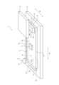
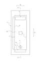
図3~図5に示す第1実施形態に係る基板固定構造1は、センサ2と、センサ2を実装される基板3と、基板3を固定される被固定部4と、基板3の第1主面3aの第1部分5を被固定部4に固着する固着部6と、基板3の第1主面3aの第2部分7の裏側部分11に接する第1表面12aと第1表面12aの裏側の第2表面12bを有する弾性部材12と、第1主面3aに垂直な方向において被固定部4に対する位置が規制され、弾性部材12の第2表面12bに接する規制部13と、を有する。また被固定部4は、基板3の第1主面3aの第2部分7に固着されずに接する。The
第1部分5は、第1主面3aに沿う第1方向D1において基板3の一端部3bに位置し、第2部分7は、第1方向D1において基板3の他端部3cに位置し、センサ2は、第1方向D1における基板3の一端部3bと他端部3cとの間に位置する。The
固着部6は、基板3と被固定部4を締結する締結具10によって形成される。締結具10は、図示するようにボルトであってもよいし、リベットなどであってもよい。なお、図3は締結具10を締結する前の状態を示す。固着部6は、締結具10に限らず、接着部又は溶着部などによって形成してもよい。The
被固定部4は、基板3を第1主面3aに沿う方向に位置決めするように基板3に接する第1位置決め部14を有する。第1位置決め部14は、基板3を第1方向D1に位置決めする。より具体的には、第1位置決め部14は、基板3の側面3fに接することで基板3を位置決めする。第1位置決め部14は凸状をなす。第1位置決め部14は単一の凸部で形成してもよいし、複数の凸部で形成してもよいし、凸部の形状は適宜設定できる。The fixed
被固定部4は、第1主面3aに沿い第1方向D1に垂直な第2方向D2に基板3を位置決めする第2位置決め部15を有する。第2位置決め部15は、基板3の側面3fに接することで基板3を位置決めする。第2位置決め部15は、少なくとも基板3における第1方向D1の他端側の部分を位置決めする。第2位置決め部15は凸状をなす。第2位置決め部15は単一の凸部で形成してもよいし、複数の凸部で形成してもよいし、凸部の形状は適宜設定できる。The fixed
基板3は、第1方向D1の幅と第2方向D2の幅が何れも第1主面3aに垂直な方向の幅よりも大きい板状をなす。換言すれば、基板3は、第1主面3aとその反対側の第2主面3gがその他の面よりも大きい板状をなす。なお、説明の便宜上、第1主面3aに垂直な方向を上下方向ともいい、第1主面3aから第2主面3gに向かう側を上側ともいい、その反対側を下側ともいう。The
基板3は、第1方向D1に沿って延びる2つの側面3fと、第2方向D2に沿って延びる2つの側面3fと、を有する。つまり、基板3は、上面視で矩形状をなす矩形板状をなす。なお、基板3は矩形板状に限らず、例えば円板状などに構成してもよい。The
基板3は平板状をなし、被固定部4は、平面状の第1主面3aに沿うように平面状をなす被固定面4aを有する。被固定面4aは、基板3の第1主面3aの第1部分5と第2部分7に接する。なお、基板3は平板状に限らず、例えば上側又は下側に突出する球面状又は円柱面状などの曲面状板状に構成してもよく、この場合、被固定面4aの形状は基板3の形状に合わせて適宜設定できる。The
弾性部材12は、例えばゴム又はエラストマーなどによって形成される。弾性部材12の形状は、基板3の第1主面3aの第2部分7の裏側部分11に接する第1表面12a(下面)と第1表面12aの裏側の第2表面12b(上面)を有する範囲で適宜設定でき、図示するような板状に限らない。組み立て性を考慮し、弾性部材12を基板3と規制部13の何れか一方に固着することが好ましい。なお、弾性部材12を基板3と規制部13の何れにも固着しない構成としてもよいし、弾性部材12を基板3と規制部13の両方に固着する構成としてもよい。The
本実施形態では、規制部13が、第1主面3aに垂直な方向において被固定部4に対する位置が規制され、弾性部材12の第2表面12bに接し、弾性部材12の第1表面12aが、基板3の第1主面3aの第2部分7の裏側部分11に接し、被固定部4が、基板3の第1主面3aの第2部分7に固着されずに接する。In this embodiment, the position of the regulating
したがって本実施形態によれば、基板3の第1主面3aの第2部分7を、第1主面3aに垂直な方向において、被固定部4の被固定面4aに接する位置に精度良く位置決めできる。またこの状態で、基板3の第1主面3aの第2部分7は被固定部4の被固定面4aに対して相対的に第1方向D1に容易に変位できるため、本実施形態によれば、基板3と被固定部4の線膨張係数が相違する場合でも、温度変化時に基板3(及び基板3上のセンサ2関連の回路部品)に生じる応力を抑制でき、もって、センサ2の測定精度に対する温度変化の影響を抑制できる。Therefore, according to this embodiment, the
また本実施形態では第1位置決め部14と第2位置決め部15により、被固定部4への基板3の位置決め精度を向上できる。In addition, in this embodiment, the
なお規制部13は、被固定部4を形成する部材と一体に設けてもよいし、別体に設けて組み付けてもよい。規制部13によって弾性部材12を基板3に押し付ける押し付け力の大きさは、位置決め精度と測定精度のバランスを考慮して適宜設定できる。押し付け力をゼロに設定してもよい。The restricting
次に、第2実施形態について説明する。Next, we will explain the second embodiment.
図6に示す第2実施形態に係る基板固定構造1は、第1位置決め部14と第2位置決め部15の構成が第1実施形態の場合とは異なり、その他の構成は第1実施形態の場合と同様である。なお、図6は締結具10を締結する前の状態を示す。The
本実施形態では、第1位置決め部14は、基板3に設けられる穴3hの側面に接することで基板3を第1方向D1に位置決めする。穴3hは基板3を上下方向に貫通する底面視円形の貫通穴からなり、第1位置決め部14は穴3hに挿入される上面視円形の凸状をなす。なお、穴3hは貫通穴に限らず、凹状をなす構成としてもよく、穴3hの形状は底面視円形に限らない。また、第1位置決め部14の形状は上面視円形に限らず、適宜設定できる。In this embodiment, the
本実施形態では、第2位置決め部15は、基板3に設けられる第1方向D1に細長い長穴3iの側面に接することで基板3を第2方向D2に位置決めする。長穴3iは基板3を上下方向に貫通する貫通穴からなり、第1位置決め部14は穴に挿入される上面視円形の凸状をなす。なお、長穴3iは貫通穴に限らず、凹状をなす構成としてもよい。第1位置決め部14の形状は上面視円形に限らず、適宜設定できる。第2位置決め部15は、基板3における第1方向D1の他端側の部分を位置決めする。In this embodiment, the
本実施形態によれば、第1実施形態の場合と同様に、センサ2の測定精度に対する温度変化の影響を抑制でき、被固定部4への基板3の良好な位置決め精度も実現できる。According to this embodiment, as in the first embodiment, the effect of temperature changes on the measurement accuracy of the
本開示は前述した実施形態に限定されず、その要旨を逸脱しない範囲で種々変更可能である。This disclosure is not limited to the above-described embodiments, and various modifications are possible without departing from the spirit of the present disclosure.
したがって、前述した実施形態に係る基板固定構造1は、センサ2と、センサ2を実装される基板3と、基板3を固定される被固定部4と、基板3の第1主面3aの第1部分5を被固定部4に固着する固着部6と、基板3の第1主面3aの第2部分7の裏側部分11に接する第1表面12aと第1表面12aの裏側の第2表面12bを有する弾性部材12と、第1主面3aに垂直な方向において被固定部4に対する位置が規制され、弾性部材12の第2表面12bに接する規制部13と、を有し、被固定部4が、基板3の第1主面3aの第2部分7に固着されずに接する、基板固定構造1である限り、種々変更可能である。Therefore, the
例えば、被固定部4に第1位置決め部14と第2位置決め部15の何れか一方又は両方を設けない構成としてもよい。基板3上のセンサ2の配置は適宜設定できる。For example, the fixed
なお、前述した実施形態に係る基板固定構造1は、第1部分5が、第1主面3aに沿う第1方向D1において基板3の一端部3bに位置し、第2部分7が、第1方向D1において基板3の他端部3cに位置し、センサ2が、第1方向D1における基板3の一端部3bと他端部3cとの間に位置する、基板固定構造1であることが好ましい。The
前述した実施形態に係る基板固定構造1は、被固定部4が、基板3を第1主面3aに沿う方向に位置決めするように基板3に接する第1位置決め部14を有する、基板固定構造1であることが好ましい。The
前述した実施形態に係る基板固定構造1は、第1位置決め部14が、基板3を第1方向D1に位置決めする、基板固定構造1であることが好ましい。The
前述した実施形態に係る基板固定構造1は、第1位置決め部14が、基板3の側面3fに接することで基板3を位置決めする、基板固定構造1であることが好ましい。The
前述した実施形態に係る基板固定構造1は、第1位置決め部14が、基板3に設けられる穴3hの側面に接することで基板3を位置決めする、基板固定構造1であることが好ましい。The
前述した実施形態に係る基板固定構造1は、被固定部4が、第1主面3aに沿い第1方向D1に垂直な第2方向D2に基板3を位置決めする第2位置決め部15を有する、基板固定構造1であることが好ましい。The
前述した実施形態に係る基板固定構造1は、第2位置決め部15が、基板3の側面3fに接することで基板3を位置決めする、基板固定構造1であることが好ましい。The
前述した実施形態に係る基板固定構造1は、第2位置決め部15が、基板3に設けられる第1方向D1に細長い長穴3iの側面に接することで基板3を位置決めする、基板固定構造1であることが好ましい。The
前述した実施形態に係る基板固定構造1は、第2位置決め部15が、少なくとも基板3における第1方向D1の他端側の部分を位置決めする、基板固定構造1であることが好ましい。The
前述した実施形態に係る基板固定構造1は、固着部6が、基板3と被固定部4を締結するボルト又はリベットなどの締結具10によって形成される、基板固定構造1であることが好ましい。The
前述した実施形態に係る基板固定構造1は、固着部6が接着部又は溶着部によって形成される、基板固定構造1であることが好ましい。The
前述した実施形態に係る基板固定構造1は、第1位置決め部14が凸状をなす、基板固定構造1であることが好ましい。The
前述した実施形態に係る基板固定構造1は、第2位置決め部15が凸状をなす、基板固定構造1であることが好ましい。The
1 基板固定構造
2 センサ
3 基板
3a 第1主面
3b 第1方向の一端部
3c 第1方向の他端部
3d 第2方向の一端部
3e 第2方向の他端部
3f 側面
3g 第2主面
3h 穴
3i 長穴
4 被固定部
4a 被固定面
5 第1部分
6 固着部
6a 第1固着部
6b 第2固着部
6c 第3固着部
6d 第4固着部
7 第2部分
8 第3部分
9 第4部分
10 締結具
11 裏側部分
12 弾性部材
12a 第1表面
12b 第2表面
13 規制部
14 第1位置決め部
15 第2位置決め部
D1 第1方向
D2 第2方向 REFERENCE SIGNS
Claims (9)
Translated fromJapanese前記センサを実装される基板と、
前記基板を固定される被固定部と、
前記基板の第1主面の第1部分を前記被固定部に固着する固着部と、
前記基板の前記第1主面の第2部分の裏側部分に接する第1表面と第1表面の裏側の第2表面を有する弾性部材と、
前記第1主面に垂直な方向において前記被固定部に対する位置が規制され、前記弾性部材の前記第2表面に接する規制部と、を有し、
前記被固定部が、前記基板の前記第1主面の前記第2部分に固着されずに接し、
前記第1部分が、前記第1主面に沿う第1方向において前記基板の一端部に位置し、
前記第2部分が、前記第1方向において前記基板の他端部に位置し、
前記センサが、前記第1方向における前記基板の前記一端部と前記他端部との間に位置する、基板固定構造。 A sensor;
A substrate on which the sensor is mounted;
A fixed portion to which the substrate is fixed;
a fixing portion that fixes a first portion of the first main surface of the substrate to the fixed portion;
an elastic member having a first surface in contact with a back portion of the second portion of the first main surface of the substrate and a second surface on the back side of the first surface;
a restricting portion whose position with respect to the fixed portion is restricted in a direction perpendicular to the first main surface and which contacts the second surface of the elastic member;
the fixed portion isin contact with the second portion of the first main surface of the substrate without being fixed thereto;
the first portion is located at one end of the substrate in a first direction along the first main surface,
the second portion is located at the other end of the substrate in the first direction,
A substrate fixing structure, wherein the sensor is located between the one end and the other end of the substrate in the first direction .
Priority Applications (1)
| Application Number | Priority Date | Filing Date | Title |
|---|---|---|---|
| JP2022048960AJP7609107B2 (en) | 2022-03-24 | 2022-03-24 | Circuit board fixing structure |
Applications Claiming Priority (1)
| Application Number | Priority Date | Filing Date | Title |
|---|---|---|---|
| JP2022048960AJP7609107B2 (en) | 2022-03-24 | 2022-03-24 | Circuit board fixing structure |
Publications (2)
| Publication Number | Publication Date |
|---|---|
| JP2023142201A JP2023142201A (en) | 2023-10-05 |
| JP7609107B2true JP7609107B2 (en) | 2025-01-07 |
Family
ID=88205386
Family Applications (1)
| Application Number | Title | Priority Date | Filing Date |
|---|---|---|---|
| JP2022048960AActiveJP7609107B2 (en) | 2022-03-24 | 2022-03-24 | Circuit board fixing structure |
Country Status (1)
| Country | Link |
|---|---|
| JP (1) | JP7609107B2 (en) |
Citations (5)
| Publication number | Priority date | Publication date | Assignee | Title |
|---|---|---|---|---|
| JP2006208078A (en) | 2005-01-26 | 2006-08-10 | Matsushita Electric Ind Co Ltd | Gas sensor |
| JP2014240675A (en) | 2013-06-11 | 2014-12-25 | トヨタ自動車株式会社 | Structure for fastening control board to metallic case of on-vehicle power control unit |
| JP2015023087A (en) | 2013-07-17 | 2015-02-02 | 三菱電機株式会社 | Substrate fixing structure |
| JP2019204930A (en) | 2018-05-25 | 2019-11-28 | 株式会社Soken | Electrical machine |
| JP2021132131A (en) | 2020-02-20 | 2021-09-09 | 株式会社デンソー | Electronic device |
- 2022
- 2022-03-24JPJP2022048960Apatent/JP7609107B2/enactiveActive
Patent Citations (5)
| Publication number | Priority date | Publication date | Assignee | Title |
|---|---|---|---|---|
| JP2006208078A (en) | 2005-01-26 | 2006-08-10 | Matsushita Electric Ind Co Ltd | Gas sensor |
| JP2014240675A (en) | 2013-06-11 | 2014-12-25 | トヨタ自動車株式会社 | Structure for fastening control board to metallic case of on-vehicle power control unit |
| JP2015023087A (en) | 2013-07-17 | 2015-02-02 | 三菱電機株式会社 | Substrate fixing structure |
| JP2019204930A (en) | 2018-05-25 | 2019-11-28 | 株式会社Soken | Electrical machine |
| JP2021132131A (en) | 2020-02-20 | 2021-09-09 | 株式会社デンソー | Electronic device |
Also Published As
| Publication number | Publication date |
|---|---|
| JP2023142201A (en) | 2023-10-05 |
Similar Documents
| Publication | Publication Date | Title |
|---|---|---|
| JP4196904B2 (en) | Electronic control unit | |
| JP4129027B2 (en) | Semiconductor device | |
| JP7584202B2 (en) | Brackets for electronic control components | |
| US8351211B2 (en) | Attachment structure of an attached-plate of a substrate | |
| US20090298357A1 (en) | Electronic device and ground connection structure | |
| JP5874513B2 (en) | Board fixing structure | |
| US11794687B2 (en) | Seat belt anchor device | |
| JP5107283B2 (en) | clip | |
| JP7609107B2 (en) | Circuit board fixing structure | |
| US20240409046A1 (en) | Electronic control component bracket | |
| JP4006000B2 (en) | Electrical connector for flat flexible cable | |
| JP5513848B2 (en) | Inductor | |
| JP2012064985A (en) | Substrate holding/fixing structure | |
| JP4999060B2 (en) | Heat receiving member mounting structure | |
| TWI693876B (en) | Circuit board and battery base thereof | |
| JP5708002B2 (en) | socket | |
| JP2004335781A (en) | Mounting structure of coil device | |
| JP2025144930A (en) | fixed structure | |
| JP2005311220A (en) | Implementation structure for heat sink | |
| JP2005072530A (en) | Fixing device | |
| JP2015105743A (en) | Fixing structure | |
| JPH10308482A (en) | Cpu cooling structure | |
| JP2008172110A (en) | Holding structure that fixes multiple member heights uniformly at the same time | |
| WO2013051058A1 (en) | Push button structure and electronic device using same | |
| JP2000067699A (en) | Switch button and switch device |
Legal Events
| Date | Code | Title | Description |
|---|---|---|---|
| A621 | Written request for application examination | Free format text:JAPANESE INTERMEDIATE CODE: A621 Effective date:20240401 | |
| A977 | Report on retrieval | Free format text:JAPANESE INTERMEDIATE CODE: A971007 Effective date:20240926 | |
| A131 | Notification of reasons for refusal | Free format text:JAPANESE INTERMEDIATE CODE: A131 Effective date:20241001 | |
| A521 | Request for written amendment filed | Free format text:JAPANESE INTERMEDIATE CODE: A523 Effective date:20241108 | |
| TRDD | Decision of grant or rejection written | ||
| A01 | Written decision to grant a patent or to grant a registration (utility model) | Free format text:JAPANESE INTERMEDIATE CODE: A01 Effective date:20241119 | |
| A61 | First payment of annual fees (during grant procedure) | Free format text:JAPANESE INTERMEDIATE CODE: A61 Effective date:20241202 | |
| R150 | Certificate of patent or registration of utility model | Ref document number:7609107 Country of ref document:JP Free format text:JAPANESE INTERMEDIATE CODE: R150 |