Movatterモバイル変換


[0]ホーム

URL:


JP7608909B2 - Movable device, deflection device, object recognition device, image projection device, and moving body - Google Patents

Movable device, deflection device, object recognition device, image projection device, and moving body
Download PDF

Info

Publication number
JP7608909B2
JP7608909B2JP2021047767AJP2021047767AJP7608909B2JP 7608909 B2JP7608909 B2JP 7608909B2JP 2021047767 AJP2021047767 AJP 2021047767AJP 2021047767 AJP2021047767 AJP 2021047767AJP 7608909 B2JP7608909 B2JP 7608909B2
Authority
JP
Japan
Prior art keywords
movable
axis
movable device
reflecting
scanning
Prior art date
Legal status (The legal status is an assumption and is not a legal conclusion. Google has not performed a legal analysis and makes no representation as to the accuracy of the status listed.)
Active
Application number
JP2021047767A
Other languages
Japanese (ja)
Other versions
JP2022146675A (en
Inventor
慎一 原田
正幸 藤島
宣就 塚本
Current Assignee (The listed assignees may be inaccurate. Google has not performed a legal analysis and makes no representation or warranty as to the accuracy of the list.)
Ricoh Co Ltd
Original Assignee
Ricoh Co Ltd
Priority date (The priority date is an assumption and is not a legal conclusion. Google has not performed a legal analysis and makes no representation as to the accuracy of the date listed.)
Filing date
Publication date
Application filed by Ricoh Co LtdfiledCriticalRicoh Co Ltd
Priority to JP2021047767ApriorityCriticalpatent/JP7608909B2/en
Publication of JP2022146675ApublicationCriticalpatent/JP2022146675A/en
Application grantedgrantedCritical
Publication of JP7608909B2publicationCriticalpatent/JP7608909B2/en
Activelegal-statusCriticalCurrent
Anticipated expirationlegal-statusCritical

Links

Images

Landscapes

Description

Translated fromJapanese

本発明は、可動装置、偏向装置、物体認識装置、画像投影装置、及び移動体に関する。The present invention relates to a movable device, a deflection device, an object recognition device, an image projection device, and a moving body.

近年、半導体製造技術を応用したマイクロマシニング技術の発達に伴い、シリコン又はガラスを微細加工して製造されるMEMS(Micro Electro Mechanical Systems)デバイスの開発が進んでいる。In recent years, with the advancement of micromachining technology that applies semiconductor manufacturing technology, there has been progress in the development of MEMS (Micro Electro Mechanical Systems) devices that are manufactured by microfabricating silicon or glass.

MEMSデバイスとしては、例えば、反射部を有する可動部と、可動部に接続し、可動部を駆動させる第1駆動部と、第1駆動部に接続し、第1駆動部を支持する第1支持部と、を有する可動装置が知られている。この可動装置では、可動部は、反射部を挟んで対称に配置された調整部を含む(例えば、特許文献1参照)。As an example of a MEMS device, a movable device is known that has a movable part having a reflecting part, a first driving part connected to the movable part and driving the movable part, and a first support part connected to the first driving part and supporting the first driving part. In this movable device, the movable part includes adjustment parts that are arranged symmetrically on either side of the reflecting part (see, for example, Patent Document 1).

この可動装置において、調整部は、可動部の重量の対称性を確保する部分であり、調整部を設けて可動部の重量の対称性を確保することで、可動部の重心位置のずれを防止し、可動部の回動の安定性を確保している。In this movable device, the adjustment unit is a part that ensures the symmetry of the weight of the movable part. By providing the adjustment unit and ensuring the symmetry of the weight of the movable part, the center of gravity of the movable part is prevented from shifting, and the stability of the rotation of the movable part is ensured.

ところで、上記の可動装置において、反射部は、重力の影響を受けて、Z方向(重力方向)の位置及び設置方向が変わる。これにより、反射部の走査角及び走査中心が変化する。反射部の走査角及び走査中心が変化すると、例えば、可動装置を物体との距離を測定するセンシング技術等に応用する場合に、測定結果の精度を悪化させる要因になりえる。しかし、上記の可動装置では、重力の影響による反射部の走査角の変化及び走査中心の変化に改善の余地があった。In the above-mentioned movable device, the reflecting part is affected by gravity and changes its position and installation direction in the Z direction (gravity direction). This causes the scanning angle and scanning center of the reflecting part to change. If the scanning angle and scanning center of the reflecting part change, for example, when the movable device is applied to sensing technology that measures the distance to an object, this can cause the accuracy of the measurement results to deteriorate. However, in the above-mentioned movable device, there was room for improvement in the change in the scanning angle and scanning center of the reflecting part due to the effect of gravity.

本発明は、上記の点に鑑みてなされたものであって、重力の影響による反射部の走査角の変化及び走査中心の変化を抑制可能な可動装置を提供することを課題とする。The present invention has been made in consideration of the above points, and aims to provide a movable device that can suppress changes in the scanning angle of the reflecting part and changes in the scanning center caused by the influence of gravity.

開示の技術の一態様に係る可動装置は、所定の軸を中心に回動可能な可動部と、前記可動部に一端が接続され、前記可動部を回動させる駆動部と、を備え、前記可動部は、前記所定の軸が伸びる方向に延出する延出部を有し、平面視で、前記可動部は、前記延出部の長手方向の端部に、前記駆動部とは反対側に突出する突出部を有する
A movable device according to one aspect of the disclosed technology comprises a movable part that can rotate around a predetermined axis, and a drive part having one end connected to the movable part and rotating the movable part, wherein the movable parthas an extension part that extends in the direction in which the predetermined axis extends, and in a planar view, the movable part has a protrusion at a longitudinal end of the extension part that protrudes on the opposite side to the drive part .

開示の技術によれば、重力の影響による反射部の走査角の変化及び走査中心の変化を抑制可能な可動装置を提供できる。The disclosed technology can provide a movable device that can suppress changes in the scanning angle of the reflecting part and changes in the scanning center caused by the effects of gravity.

第1実施形態に係る可動装置である光偏向器の平面図(反射面側から視た図)である。FIG. 2 is a plan view (as viewed from the reflecting surface side) of the optical deflector which is a movable device according to the first embodiment.第1実施形態に係る可動装置である光偏向器の底面図(反射面とは反対側から視た図)である。FIG. 2 is a bottom view (as viewed from the side opposite to the reflecting surface) of the optical deflector which is the movable device according to the first embodiment.図1のA-A線に沿う断面図である。2 is a cross-sectional view taken along line AA in FIG. 1.図1のB-B線に沿う断面図である。2 is a cross-sectional view taken along line BB in FIG. 1.第1実施形態に係る可動装置である光偏向器の部分底面図(反射面とは反対側から視た図)である。FIG. 2 is a partial bottom view (as viewed from the side opposite to the reflecting surface) of the optical deflector which is the movable device according to the first embodiment.図5のC-C線に沿う断面図である。6 is a cross-sectional view taken along line CC of FIG. 5.第1実施形態の変形例1に係る可動装置である光偏向器の平面図(反射面側から視た図)である。FIG. 11 is a plan view (viewed from the reflecting surface side) of an optical deflector which is a movable device according to a first modified example of the first embodiment.第1実施形態の変形例2に係る可動装置である光偏向器の平面図(反射面側から視た図)である。FIG. 11 is a plan view (viewed from the reflecting surface side) of an optical deflector which is a movable device according to a second modified example of the first embodiment.第1実施形態の変形例3に係る可動装置である光偏向器の平面図(反射面側から視た図)である。FIG. 11 is a plan view (viewed from the reflecting surface side) of an optical deflector which is a movable device according to a third modified example of the first embodiment.第2実施形態に係る可動装置である光偏向器の平面図(反射面側から視た図)である。FIG. 11 is a plan view (as viewed from the reflecting surface side) of an optical deflector which is a movable device according to a second embodiment.第2実施形態に係る可動装置である光偏向器の底面図(反射面とは反対側から視た図)である。FIG. 11 is a bottom view (as viewed from the side opposite to the reflecting surface) of the optical deflector which is a movable device according to the second embodiment.第2実施形態の変形例1に係る可動装置である光偏向器の平面図(反射面側から視た図)である。FIG. 13 is a plan view (as viewed from the reflecting surface side) of an optical deflector which is a movable device according to a first modified example of the second embodiment.第3実施形態に係る可動装置である光偏向器の平面図(反射面側から視た図)である。FIG. 11 is a plan view (as viewed from the reflecting surface side) of an optical deflector which is a movable device according to a third embodiment.第3実施形態の変形例1に係る可動装置である光偏向器の平面図(反射面側から視た図)である。FIG. 13 is a plan view (as viewed from the reflecting surface side) of an optical deflector which is a movable device according to a first modified example of the third embodiment.光走査システムの一例の概略図である。1 is a schematic diagram of an example optical scanning system.光走査システムの一例のハードウェア構成図である。FIG. 2 is a diagram illustrating a hardware configuration of an example of an optical scanning system.駆動装置の一例の機能ブロック図である。FIG. 2 is a functional block diagram of an example of a drive device.光走査システムに係る処理の一例のフローチャートである。13 is a flowchart of an example of a process related to the optical scanning system.ヘッドアップディスプレイ装置を搭載した自動車の一例の概略図である。1 is a schematic diagram of an example of an automobile equipped with a head-up display device.ヘッドアップディスプレイ装置の一例の概略図である。1 is a schematic diagram of an example of a head-up display device.光書込装置を搭載した画像形成装置の一例の概略図である。1 is a schematic diagram of an example of an image forming apparatus equipped with an optical writing device.光書込装置の一例の概略図である。FIG. 1 is a schematic diagram of an example of an optical writing device.レーザレーダ装置を搭載した自動車の一例の概略図である。1 is a schematic diagram of an example of an automobile equipped with a laser radar device.レーザレーダ装置の一例の概略図である。FIG. 1 is a schematic diagram of an example of a laser radar device.パッケージングされた光偏向器の一例の概略図である。FIG. 2 is a schematic diagram of an example of a packaged optical deflector.

以下、図面を参照して発明を実施するための形態について説明する。各図面において、同一構成部分には同一符号を付し、重複した説明を省略する場合がある。Below, a description will be given of a mode for carrying out the invention with reference to the drawings. In each drawing, the same components are given the same reference numerals, and duplicated explanations may be omitted.

なお、以下の実施形態の説明では、実施形態の用語における回動、揺動、可動は同義であるとする。さらに、矢印により示した方向のうち、X方向は回転軸となる第1軸と平行な方向、Y方向は第1軸と垂直な方向、Z方向はXY平面と直交する方向とする。In the following description of the embodiment, the terms rotation, swing, and movement are synonymous. Furthermore, among the directions indicated by the arrows, the X direction is parallel to the first axis that is the axis of rotation, the Y direction is perpendicular to the first axis, and the Z direction is perpendicular to the XY plane.

〈第1実施形態〉
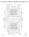
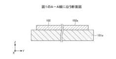
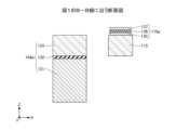
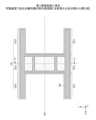
図1は、第1実施形態に係る可動装置である光偏向器の平面図(反射面側から視た図)である。図2は、第1実施形態に係る可動装置である光偏向器の底面図(反射面とは反対側から視た図)である。図3は、図1のA-A線に沿う断面図である。図4は、図1のB-B線に沿う断面図である。
First Embodiment
Fig. 1 is a plan view (viewed from the reflecting surface side) of an optical deflector which is a movable device according to the first embodiment. Fig. 2 is a bottom view (viewed from the opposite side to the reflecting surface) of the optical deflector which is a movable device according to the first embodiment. Fig. 3 is a cross-sectional view taken along line A-A in Fig. 1. Fig. 4 is a cross-sectional view taken along line B-B in Fig. 1.

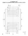
図1~図4を参照すると、可動装置100は、両端支持構造の光偏向器である。可動装置100は、主に、可動部101と、反射部102と、駆動部103a及び103bと、支持部104a及び104bとを有している。可動装置100は、反射部102を含む可動部101をX軸に平行な第1軸AX1を中心に回動可能にする構造を備えている。すなわち、可動装置100は、反射部102を含む可動部101が1軸方向(第1軸AX1の周り)に回動することにより、入射する光を1軸方向に走査しながら偏向可能である。以下、可動装置100の構造について詳説する。Referring to Figures 1 to 4, themovable device 100 is an optical deflector with a support structure at both ends. Themovable device 100 mainly has amovable part 101, a reflectingpart 102,driving parts 103a and 103b, and supportingparts 104a and 104b. Themovable device 100 has a structure that allows themovable part 101 including thereflecting part 102 to rotate around a first axis AX1 parallel to the X-axis. In other words, themovable device 100 can deflect incident light while scanning it in one axial direction by rotating themovable part 101 including thereflecting part 102 in one axial direction (around the first axis AX1). The structure of themovable device 100 will be described in detail below.

可動部101は、中央部101aと、延出部101b及び101cとを有する。中央部101aは、例えば、X方向の長さよりもY方向の長さが長い矩形状であり、第1軸AX1を跨ぐように配置されている。Themovable part 101 has acentral part 101a andextension parts 101b and 101c. Thecentral part 101a is, for example, rectangular in shape with a length in the Y direction longer than its length in the X direction, and is positioned so as to straddle the first axis AX1.

延出部101bは、中央部101aの+Y側端部(第1軸AX1に直交する方向の一端部)の両側から第1軸AX1が伸びる方向に延出している。延出部101cは、中央部101aの-Y側端部(第1軸AX1に直交する方向の他端部)の両側から第1軸AX1が伸びる方向に延出している。延出部101b及び101cは、例えば、Y方向の長さよりもX方向の長さが長い矩形状である。図1の例では、延出部101b及び101cは一定幅である。しかし、これには限らず、延出部101b及び101cは部分的に幅が異なっていてもよい。Theextension portion 101b extends in the direction of the first axis AX1 from both sides of the +Y end (one end in the direction perpendicular to the first axis AX1) of thecentral portion 101a. Theextension portion 101c extends in the direction of the first axis AX1 from both sides of the -Y end (the other end in the direction perpendicular to the first axis AX1) of thecentral portion 101a. Theextension portions 101b and 101c are, for example, rectangular in shape with a longer length in the X direction than in the Y direction. In the example of FIG. 1, theextension portions 101b and 101c have a constant width. However, this is not limited to this, and theextension portions 101b and 101c may have partially different widths.

ここで、『第1軸AX1が伸びる方向に延出する』とは、対象物が第1軸AX1と直交する方向以外の方向に伸びていることである。すなわち、延出部101b及び101cは、第1軸AX1と直交する方向以外の方向に伸びていればよく、第1軸AX1に対して傾斜していてもよい。ただし、可動装置100の大型化を抑制する観点から、図1に示すように、延出部101b及び101cは、長手方向が第1軸AX1と平行であることが好ましい。Here, "extending in the direction in which the first axis AX1 extends" means that the object extends in a direction other than the direction perpendicular to the first axis AX1. In other words, theextensions 101b and 101c may extend in a direction other than the direction perpendicular to the first axis AX1, and may be inclined with respect to the first axis AX1. However, from the viewpoint of preventing the size of themovable device 100 from increasing, it is preferable that the longitudinal direction of theextensions 101b and 101c is parallel to the first axis AX1, as shown in FIG. 1.

なお、本願において、『平行』とは、2つの直線や辺等が0°±5°の範囲にある場合を含むものとする。また、『垂直』又は『直交』とは、2つの直線や辺等が90°±5°の範囲にある場合を含むものとする。ただし、個別に特別な説明がある場合は、この限りではない。また、『中心』や『中央』は、対象物のおおよその中心や中央を示すものであり、厳密な中心や中央を示すものではない。すなわち、製造誤差程度のばらつきは、許容されるものとする。点対称や線対称等についても同様である。In this application, "parallel" includes cases where two lines or sides are within the range of 0°±5°. Furthermore, "perpendicular" or "orthogonal" includes cases where two lines or sides are within the range of 90°±5°. However, this does not apply unless there is a special explanation for each case. Furthermore, "center" and "middle" refer to the approximate center or middle of an object, and do not refer to the exact center or middle. In other words, variations on the scale of manufacturing errors are permitted. The same applies to point symmetry and line symmetry.

反射部102は、可動部101上に形成されている。具体的には、反射部102は、中央部101aの+Z側の面の大部分に設けられている。反射部102は、延出部101b及び101cの一部又は全部に形成されてもよい。反射部102は、図1の例では矩形状であるが、円形状、楕円形状、又は他の複雑な形状であってもよい。反射部102は、例えば、アルミニウム、金、若しくは銀等を含む金属薄膜、又はその多層膜で構成される。反射面102aは、反射部102の+Z側の面である。Thereflective portion 102 is formed on themovable portion 101. Specifically, thereflective portion 102 is provided on most of the surface on the +Z side of thecentral portion 101a. Thereflective portion 102 may be formed on a part or all of theextension portions 101b and 101c. Thereflective portion 102 is rectangular in the example of FIG. 1, but may be circular, elliptical, or another complex shape. Thereflective portion 102 is composed of, for example, a thin metal film containing aluminum, gold, silver, or the like, or a multilayer film thereof. Thereflective surface 102a is the surface on the +Z side of thereflective portion 102.

駆動部103a及び103bは、可動部101に一端が直接又は間接に接続され、可動部101を回動させる。すなわち、駆動部103a及び103bは、反射部102を含む可動部101を回動可能な状態で支持する1対のアクチュエータである。駆動部103a及び103bは、振動梁となる複数の梁部115と、隣接する梁部115同士を接続する接続部116とを有している。駆動部103a及び103bにおいて、隣接する梁部115同士は、+Y側及び-Y側が接続部116により交互に接続されてミアンダ構造を形成している。なお、接続部116は、隣接する梁部115の長手方向の端部同士を接続せずに、隣接する梁部115の長手方向の端部よりも手前の部分同士を接続してもよい。The drivingunits 103a and 103b have one end directly or indirectly connected to themovable unit 101, and rotate themovable unit 101. In other words, the drivingunits 103a and 103b are a pair of actuators that support themovable unit 101 including the reflectingunit 102 in a rotatable state. The drivingunits 103a and 103b havemultiple beams 115 that serve as vibrating beams, and connectingunits 116 that connectadjacent beams 115 to each other. In the drivingunits 103a and 103b, the +Y side and the -Y side ofadjacent beams 115 are alternately connected by the connectingunits 116 to form a meander structure. Note that the connectingunits 116 may connect the portions ofadjacent beams 115 that are closer to the longitudinal ends of thebeams 115 to each other, without connecting the longitudinal ends of thebeams 115 to each other.

駆動部103aの+X側かつ-Y側端部は、可動部接続部117aを介し可動部101の中央部101aに接続されている。また、駆動部103aの-X側かつ-Y側端部は、支持部接続部118aを介して支持部104aに接続されている。また、駆動部103bの-X側かつ+Y側端部は、可動部接続部117bを介し可動部101の中央部101aに接続されている。また、駆動部103bの+X側かつ+Y側端部は、支持部接続部118bを介して支持部104bに接続されている。なお、図1の例では、支持部104a及び104bは、可動部101のX方向両側に配置されている。支持部104aは駆動部103aを支持し、支持部104bは駆動部103bを支持する。The +X and -Y end of thedrive unit 103a is connected to thecenter 101a of themovable unit 101 via the movableunit connection part 117a. The -X and -Y end of thedrive unit 103a is connected to thesupport unit 104a via the supportunit connection part 118a. The -X and +Y end of thedrive unit 103b is connected to thecenter 101a of themovable unit 101 via the movableunit connection part 117b. The +X and +Y end of thedrive unit 103b is connected to thesupport unit 104b via the supportunit connection part 118b. In the example of FIG. 1, thesupport units 104a and 104b are disposed on both sides of themovable unit 101 in the X direction. Thesupport unit 104a supports thedrive unit 103a, and thesupport unit 104b supports thedrive unit 103b.

中央部101aの-X側に位置する梁部115の+Z側の面の上には、梁部115ごとに、交互に駆動素子郡119aと駆動素子郡119bが設けられている。同様に、中央部101aの+X側に位置する梁部115の+Z側の面の上には、梁部115ごとに、交互に駆動素子郡119aと駆動素子郡119bが設けられている。駆動素子郡119a及び119bは、例えば、圧電素子である。On the +Z side surface of thebeam portion 115 located on the -X side of thecentral portion 101a, drivingelement groups 119a and drivingelement groups 119b are provided alternately for eachbeam portion 115. Similarly, on the +Z side surface of thebeam portion 115 located on the +X side of thecentral portion 101a, drivingelement groups 119a and drivingelement groups 119b are provided alternately for eachbeam portion 115. Drivingelement groups 119a and 119b are, for example, piezoelectric elements.

可動装置100は、例えば、可動部101の中心に対して点対称に形成することができる。しかし、これには限らず、可動装置100は、例えば、第1軸AX1に垂直で可動部101の中心を通る直線に対して線対称に形成してもよい。Themovable device 100 can be formed, for example, point-symmetrically with respect to the center of themovable part 101. However, this is not limited thereto, and themovable device 100 can be formed, for example, line-symmetrically with respect to a straight line that is perpendicular to the first axis AX1 and passes through the center of themovable part 101.

可動装置100は、例えば、1枚のSOI(Silicon On Insulator)基板をエッチング処理等により成形し、成形した基板上に反射部102並びに駆動素子郡119a及び119b等を形成することで、各構成部が一体的に形成されている。SOI基板は、単結晶シリコン(Si)からなるシリコン支持層の上に酸化シリコン層が設けられ、酸化シリコン層の上に更に単結晶シリコンからなるシリコン活性層が設けられた基板である。Themovable device 100 is formed by, for example, forming a single SOI (Silicon On Insulator) substrate by etching or the like, and forming thereflector 102 and the drivingelement groups 119a and 119b on the formed substrate, so that each component is integrally formed. The SOI substrate is a substrate in which a silicon oxide layer is provided on a silicon support layer made of single crystal silicon (Si), and a silicon active layer made of single crystal silicon is further provided on the silicon oxide layer.

シリコン活性層は、X方向又はY方向に対してZ方向への厚みが小さいため、シリコン活性層のみで構成された部材は、弾性を有する弾性部としての機能を備える。シリコン活性層の厚みは、例えば、20~60μm程度である。なお、SOI基板は、必ず平面状である必要はなく、曲率等を有していてもよい。Since the silicon active layer has a smaller thickness in the Z direction than in the X or Y direction, a member consisting of only the silicon active layer functions as an elastic part. The thickness of the silicon active layer is, for example, about 20 to 60 μm. Note that the SOI substrate does not necessarily have to be flat, and may have a curvature, etc.

可動部101の中央部101aは、例えば、シリコン活性層により形成されており、シリコン活性層の+Z側の面に反射部102が形成されている。可動部101の延出部101b及び101cも、中央部101aと同様に、例えば、シリコン活性層により形成されている。Thecentral portion 101a of themovable portion 101 is formed, for example, from a silicon active layer, and a reflectingportion 102 is formed on the +Z side surface of the silicon active layer. The extendingportions 101b and 101c of themovable portion 101 are also formed, for example, from a silicon active layer, similar to thecentral portion 101a.

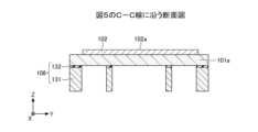
図4に示すように、支持部104aは、例えば、順次積層されたシリコン支持層131、酸化シリコン層132、及びシリコン活性層133により形成されている。支持部104bについても同様である。梁部115は、例えば、シリコン活性層により形成されている。As shown in FIG. 4, thesupport portion 104a is formed, for example, of asilicon support layer 131, asilicon oxide layer 132, and a siliconactive layer 133, which are stacked in sequence. The same is true for thesupport portion 104b. Thebeam portion 115 is formed, for example, of the silicon active layer.

駆動素子郡119a及び119bの各々は圧電素子であり、例えば、梁部115の+Z側の面上に順次形成された下部電極135、圧電部136、及び上部電極137を有している。下部電極135及び上部電極137は、例えば、金(Au)又は白金(Pt)等を用いてスパッタリング法等により形成できる。圧電部136は、例えば、圧電材料であるPZT(チタン酸ジルコン酸鉛)から形成できるが、その他の圧電材料であってもよく、種類は問わない。圧電部136の厚さは、例えば、2μm程度である。Each of the drivingelement groups 119a and 119b is a piezoelectric element, and has, for example, alower electrode 135, a piezoelectric portion 136, and anupper electrode 137 formed in sequence on the +Z side surface of thebeam portion 115. Thelower electrode 135 and theupper electrode 137 can be formed by a sputtering method or the like using, for example, gold (Au) or platinum (Pt). The piezoelectric portion 136 can be formed, for example, from PZT (lead zirconate titanate), which is a piezoelectric material, but can also be other piezoelectric materials, and any type is acceptable. The thickness of the piezoelectric portion 136 is, for example, about 2 μm.

駆動素子郡119a及び119bの下部電極135と上部電極137との間に電圧信号を印加すると、反射部102を含む可動部101は、第1軸AX1の周りに回動する。具体的には、駆動素子郡119a及び119bにおいて、支持部104a及び104b側からそれぞれ奇数番目の梁部115と偶数番目の梁部115をセットで交互に逆相で駆動する。When a voltage signal is applied between thelower electrode 135 and theupper electrode 137 of the drivingelement groups 119a and 119b, themovable portion 101 including the reflectingportion 102 rotates around the first axis AX1. Specifically, in the drivingelement groups 119a and 119b, the odd-numberedbeam portions 115 and the even-numberedbeam portions 115 are alternately driven in opposite phases as a set from thesupport portions 104a and 104b, respectively.

例えば、下部電極135と上部電極137との間にパルス波又は正弦波の電圧信号を印加すると、駆動素子郡119a及び119bは、その電歪特性によって梁部115の表面の面内方向において伸縮を繰り返す。これにより、梁部115が曲げ振動してミアンダ構造が交互に上下運動し、さらにミアンダ構造の上下運動が回転振動(捻り振動)に変換され、反射部102を含む可動部101が第1軸AX1の周りに回動する。For example, when a pulse wave or sine wave voltage signal is applied between thelower electrode 135 and theupper electrode 137, the drivingelement groups 119a and 119b repeatedly expand and contract in the in-plane direction of the surface of thebeam portion 115 due to their electrostrictive properties. This causes thebeam portion 115 to vibrate in bending, causing the meandering structure to move up and down alternately, and the up and down movement of the meandering structure is further converted into rotational vibration (torsional vibration), causing themovable portion 101 including the reflectingportion 102 to rotate around the first axis AX1.

なお、図1においては、駆動素子郡119a及び119bは、梁部115の一部に設けられている。しかし、駆動素子郡119a及び119bは、必ずしも梁部115の一部に設けられている必要はなく、梁部115の全面に設けられてもよい。また、駆動素子郡119a及び119bは、全ての梁部115に設けられている必要はなく、複数の梁部115のうち、一部のみに設けられてもよい。In FIG. 1, the drivingelement groups 119a and 119b are provided on a portion of thebeam portion 115. However, the drivingelement groups 119a and 119b do not necessarily have to be provided on a portion of thebeam portion 115, and may be provided on the entire surface of thebeam portion 115. Also, the drivingelement groups 119a and 119b do not necessarily have to be provided on all of thebeam portions 115, and may be provided on only a portion of themultiple beam portions 115.

また、上部電極137の+Z側の面上、並びに支持部104a及び104bの+Z側の面上の少なくともいずれかに酸化シリコン層等からなる絶縁層が形成されていてもよい。このとき、絶縁層の上に電極配線を設け、また、下部電極135又は上部電極137と電極配線とが接続される接続スポットのみ、開口部として部分的に絶縁層を除去又は絶縁層を形成しないことが好ましい。これにより、駆動部103a及び103b並びに電極配線の設計自由度を向上し、更に電極同士の接触による短絡を抑制できる。また、酸化シリコン層は、反射防止材としての機能を備えてもよい。An insulating layer made of a silicon oxide layer or the like may be formed on at least one of the +Z side surface of theupper electrode 137 and the +Z side surfaces of thesupport parts 104a and 104b. In this case, it is preferable to provide electrode wiring on the insulating layer, and to partially remove the insulating layer as an opening or not form the insulating layer only at the connection spot where thelower electrode 135 or theupper electrode 137 is connected to the electrode wiring. This improves the design freedom of thedrive parts 103a and 103b and the electrode wiring, and further suppresses short circuits due to contact between the electrodes. The silicon oxide layer may also function as an anti-reflective material.

また、駆動素子郡119a及び119bは、圧電部が複数積層され、中間電極を含む構造のものであってもよい。In addition, the drivingelement groups 119a and 119b may have a structure in which multiple piezoelectric parts are stacked and include an intermediate electrode.

なお、以上は、可動装置100をSOI基板から形成する例を示したが、これには限らない。可動装置100は、エッチング処理等により一体的に成形でき、部分的に弾性を持たせることができる基板であれば、SOI基板以外から形成してもよい。このような基板としては、例えば、Si基板及びAl基板等が挙げられる。The above describes an example in which themovable device 100 is formed from an SOI substrate, but this is not limiting. Themovable device 100 may be formed from a substrate other than an SOI substrate as long as the substrate can be integrally molded by etching or the like and can be partially made elastic. Examples of such substrates include a Si substrate and an Al substrate.

このように、可動装置100において、可動部101は、第1軸AX1の方向に延出する延出部101b及び101cを有する。これにより、重力の影響による反射部102の走査角の変化及び走査中心の変化(-Z方向への変位)を抑制可能である。その結果、可動装置100では、高精度の光走査が可能となる。これに関して、以下に詳しく説明する。In this way, in themovable device 100, themovable part 101 hasextension parts 101b and 101c that extend in the direction of the first axis AX1. This makes it possible to suppress changes in the scanning angle and the scanning center (displacement in the -Z direction) of the reflectingpart 102 due to the influence of gravity. As a result, themovable device 100 enables highly accurate optical scanning. This will be explained in detail below.

重力の影響による反射部102の走査角の変化及び走査中心の変化は、反射部102が重力の影響を受けて-Z方向(重力方向)に変位することが一因である。反射部102の重力の影響による-Z方向の変位は、反射部102を含む可動部101の(質量)/(ばね定数)に比例する。一方、可動部101の共振周波数の変化は、反射部102を含む可動部101の(第1軸AX1の周りのねじりばね定数)/(第1軸AX1の周りの慣性モーメント)の平方根に比例する。The change in the scanning angle and the scanning center of the reflectingpart 102 due to the influence of gravity is caused in part by the reflectingpart 102 being displaced in the -Z direction (gravity direction) due to the influence of gravity. The displacement of the reflectingpart 102 in the -Z direction due to the influence of gravity is proportional to the (mass)/(spring constant) of themovable part 101 including the reflectingpart 102. On the other hand, the change in the resonant frequency of themovable part 101 is proportional to the square root of the (torsional spring constant about the first axis AX1)/(moment of inertia about the first axis AX1) of themovable part 101 including the reflectingpart 102.

ここで、ばね定数と第1軸AX1の周りのねじりバネ定数は、おおよそ比例関係にある。よって、重力の影響による反射部102の走査角の変化及び走査中心の変化は、(質量)/(第1軸AX1の周りの慣性モーメント)に比例することになる。そのため、重力の影響による反射部102の走査角の変化及び走査中心の変化を抑制するには、(質量)/(第1軸AX1の周りの慣性モーメント)を小さくすればよい。Here, the spring constant and the torsion spring constant around the first axis AX1 are roughly proportional to each other. Therefore, the change in the scanning angle and the change in the scanning center of the reflectingunit 102 due to the influence of gravity are proportional to (mass)/(moment of inertia around the first axis AX1). Therefore, in order to suppress the change in the scanning angle and the change in the scanning center of the reflectingunit 102 due to the influence of gravity, it is sufficient to reduce (mass)/(moment of inertia around the first axis AX1).

一般に、可動部101において、第1軸AX1から遠い箇所の質量が大きいほど、可動部101の第1軸AX1の周りの慣性モーメントは増加する。よって、可動部101において、第1軸AX1から離れた領域に質量を集中させると、(質量)/(第1軸AX1の周りの慣性モーメント)を小さくでき、重力の影響による反射部102の走査角の変化及び走査中心の変化を効果的に抑制できる。In general, the greater the mass of themovable part 101 at a location farther from the first axis AX1, the greater the moment of inertia of themovable part 101 about the first axis AX1. Therefore, by concentrating the mass of themovable part 101 in an area farther from the first axis AX1, it is possible to reduce (mass)/(moment of inertia about the first axis AX1), and it is possible to effectively suppress changes in the scanning angle and scanning center of the reflectingpart 102 due to the influence of gravity.

すなわち、可動装置100において、可動部101が第1軸AX1の方向に延出する延出部101b及び101cを有することで、可動部101の第1軸AX1の周りの慣性モーメントは増加する。その結果、可動部101において、(質量)/(第1軸AX1の周りの慣性モーメント)を小さくでき、重力の影響による反射部102の走査角の変化及び走査中心の変化を抑制できる。可動部101は、第1軸AX1に対して、平面形状及び質量が対称であることが好ましい。これにより、可動部101の第1軸AX1の周りの慣性モーメントをより効率的に増加させることができる。In other words, in themovable device 100, themovable part 101 hasextension parts 101b and 101c that extend in the direction of the first axis AX1, so that the moment of inertia of themovable part 101 around the first axis AX1 increases. As a result, in themovable part 101, (mass)/(moment of inertia around the first axis AX1) can be made small, and changes in the scanning angle and scanning center of the reflectingpart 102 due to the influence of gravity can be suppressed. It is preferable that the planar shape and mass of themovable part 101 are symmetrical with respect to the first axis AX1. This makes it possible to more efficiently increase the moment of inertia of themovable part 101 around the first axis AX1.

なお、可動部101の共振周波数は、(第1軸AX1の周りのねじりばね定数)/(第1軸AX1の周りの慣性モーメント)の平方根に比例するため、可動部101の第1軸AX1の周りの慣性モーメントが増加すると、可動部101の共振周波数は低下する。可動部101の共振周波数を維持するためには、可動部101のばね定数を増加させる必要があるが、可動部101のばね定数を増加させることで、重力の影響による反射部102の走査角の変化及び走査中心の変化をさらに抑制可能となる。The resonant frequency of themovable part 101 is proportional to the square root of (torsion spring constant around the first axis AX1)/(moment of inertia around the first axis AX1), so when the moment of inertia around the first axis AX1 of themovable part 101 increases, the resonant frequency of themovable part 101 decreases. In order to maintain the resonant frequency of themovable part 101, it is necessary to increase the spring constant of themovable part 101. However, by increasing the spring constant of themovable part 101, it is possible to further suppress changes in the scanning angle and the scanning center of the reflectingpart 102 due to the influence of gravity.

可動部において第1軸AX1に直交する方向の長さを増加させても上記と同様の効果が得られるが、可動装置のサイズが大きくなり、かつコストも増加するため好ましくない。本実施形態に係る可動装置100では、可動部101の延出部101b及び101cは第1軸AX1が伸びる方向に延出しており、第1軸AX1に直交する方向には延出していない。これにより、可動装置100のサイズが大きくなることが抑制しつつ、可動部101の第1軸AX1の周りの慣性モーメントを増加できるため、可動装置100の大型化抑制の点及びコストの点でも有利である。Increasing the length of the movable part in the direction perpendicular to the first axis AX1 can achieve the same effect as above, but this is not preferred as it increases the size of the movable device and the cost. In themovable device 100 of this embodiment, theextension parts 101b and 101c of themovable part 101 extend in the direction of the first axis AX1, and do not extend in a direction perpendicular to the first axis AX1. This prevents the size of themovable device 100 from increasing while increasing the moment of inertia around the first axis AX1 of themovable part 101, which is advantageous in terms of preventing the size of themovable device 100 from increasing and in terms of costs.

なお、図1において、延出部101bの-X側端部は、支持部104aの+Y側端部の最も+X側の位置よりも更に+X方向に位置していることが好ましい。また、延出部101bの+X側端部は、支持部104bの+Y側端部の最も-X側の位置よりも更に-X方向に位置していることが好ましい。また、延出部101cの-X側端部は、支持部104aの-Y側端部の最も+X側の位置よりも更に+X方向に位置していることが好ましい。また、延出部101cの+X側端部は、支持部104bの-Y側端部の最も-X側の位置よりも更に-X方向に位置していることが好ましい。In FIG. 1, the -X side end of theextension portion 101b is preferably located further in the +X direction than the +X-most position of the +Y side end of thesupport portion 104a. Also, the +X side end of theextension portion 101b is preferably located further in the -X direction than the -X-most position of the +Y side end of thesupport portion 104b. Also, the -X side end of theextension portion 101c is preferably located further in the +X direction than the +X-most position of the -Y side end of thesupport portion 104a. Also, the +X side end of theextension portion 101c is preferably located further in the -X direction than the -X-most position of the -Y side end of thesupport portion 104b.

言い換えれば、延出部101bのX方向の長さは、互いに対向する支持部104a及び104bに挟まれた領域のX方向の長さよりも短い方が好ましい。また、延出部101cのX方向の長さは、互いに対向する支持部104a及び104bに挟まれた領域のX方向の長さよりも短い方が好ましい。これらの要件を満たすことで、可動部101が回動したときに延出部101b及び101cが支持部104a及び104bに接触するおそれを低減できる。In other words, it is preferable that the length in the X direction of theextension portion 101b is shorter than the length in the X direction of the area sandwiched between the opposingsupport portions 104a and 104b. Also, it is preferable that the length in the X direction of theextension portion 101c is shorter than the length in the X direction of the area sandwiched between the opposingsupport portions 104a and 104b. By satisfying these requirements, it is possible to reduce the risk that theextension portions 101b and 101c will come into contact with thesupport portions 104a and 104b when themovable portion 101 rotates.

図5は、第1実施形態に係る可動装置である光偏向器の部分底面図(反射面とは反対側から視た図)である。図6は、図5のC-C線に沿う断面図である。Figure 5 is a partial bottom view (viewed from the side opposite the reflecting surface) of the optical deflector, which is a movable device according to the first embodiment. Figure 6 is a cross-sectional view taken along line CC in Figure 5.

図5及び図6に示すように、可動部101は、厚さ方向の一方側に突起する突起部108(リブ構造)を有してもよい。具体的には、可動部101は、裏面側(-Z側の面)に突起部108を有してもよい。突起部108は、例えば、順次積層されたシリコン支持層131及び酸化シリコン層132により構成される。酸化シリコン層132上には、シリコン活性層から形成された可動部101が位置している。As shown in Figures 5 and 6, themovable part 101 may have a protrusion 108 (rib structure) that protrudes from one side in the thickness direction. Specifically, themovable part 101 may have theprotrusion 108 on the back side (-Z side surface). Theprotrusion 108 is composed of, for example, asilicon support layer 131 and asilicon oxide layer 132 that are stacked in sequence. Themovable part 101 formed from a silicon active layer is located on thesilicon oxide layer 132.

突起部108は、例えば、中央部101aの+Y側端部及び延出部101bの裏面側、並びに中央部101aの-Y側端部及び延出部101cの裏面側に設けることができる。突起部108は、中央部101aのその他の領域、すなわち平面視で反射部102と主に重複する領域の裏面側に設けてもよい。突起部108は、延出部101b及び延出部101cの裏面側のみに設けてもよい。突起部108は、第1軸AX1に対して対称となるように設けることが好ましい。Theprotrusion 108 can be provided, for example, on the +Y side end of thecentral portion 101a and the back side of the extendingportion 101b, and on the -Y side end of thecentral portion 101a and the back side of the extendingportion 101c. Theprotrusion 108 may also be provided on the back side of other regions of thecentral portion 101a, i.e., the region that mainly overlaps with the reflectingportion 102 in a plan view. Theprotrusion 108 may be provided only on the back sides of the extendingportions 101b and 101c. It is preferable that theprotrusion 108 is provided symmetrically with respect to the first axis AX1.

なお、平面視とは、可動部101が回動していないときに、可動部101の+Z側の面の法線方向から視ることである。また、可動部101が回動していないときに、可動部101の+Z側の面の法線方向から視た形状を平面形状と称する場合がある。Note that a planar view refers to a view from the normal direction of the +Z side surface of themovable part 101 when themovable part 101 is not rotating. Also, the shape viewed from the normal direction of the +Z side surface of themovable part 101 when themovable part 101 is not rotating may be referred to as a planar shape.

このように、可動部101の裏面側に突起部108を設けることで、可動部101の第1軸AX1の周りの慣性モーメントを図1~図4の場合よりも増加させることができる。その結果、可動部101において、(質量)/(第1軸AX1の周りの慣性モーメント)を図1~図4の場合よりもさらに小さくでき、重力の影響による反射部102の走査角の変化及び走査中心の変化を図1~図4の場合よりもさらに抑制できる。In this way, by providing theprotrusion 108 on the back side of themovable part 101, the moment of inertia about the first axis AX1 of themovable part 101 can be increased more than in the cases of Figures 1 to 4. As a result, in themovable part 101, (mass)/(moment of inertia about the first axis AX1) can be made even smaller than in the cases of Figures 1 to 4, and changes in the scanning angle and scanning center of the reflectingpart 102 due to the influence of gravity can be suppressed even more than in the cases of Figures 1 to 4.

なお、可動部101の第1軸AX1の周りの慣性モーメントを効果的に増加させるためには、優先的には、第1軸AX1から離れた領域から突起部108を設けることが好ましい。しかし、図5のように、反射部102の裏面側にも突起部108を設けることは、回動中の反射部102の変形を低減できる点で好適である。また、慣性モーメントには、第1軸AX1上以外の質量が影響するため、反射部102の裏面側に突起部108を設けることも、慣性モーメントの向上に一定の効果を有する。In order to effectively increase the moment of inertia around the first axis AX1 of themovable part 101, it is preferable to provide theprotrusion 108 in an area away from the first axis AX1. However, as shown in FIG. 5, providing theprotrusion 108 on the back side of the reflectingpart 102 is preferable because it reduces deformation of the reflectingpart 102 during rotation. In addition, since the moment of inertia is affected by masses other than those on the first axis AX1, providing theprotrusion 108 on the back side of the reflectingpart 102 also has a certain effect on improving the moment of inertia.

図7は、第1実施形態の変形例1に係る可動装置である光偏向器の平面図(反射面側から視た図)である。図7に示す可動装置100Aのように、平面視で、可動部101は、延出部101bの長手方向の端部である-X側端部及び+X側端部に、駆動部103a及び103bとは反対側に突出する突出部101dを有してもよい。また、平面視で、可動部101は、延出部101cの長手方向の端部である-X側端部及び+X側端部に、駆動部103a及び103bとは反対側に突出する突出部101eを設けてもよい。Figure 7 is a plan view (viewed from the reflecting surface side) of an optical deflector, which is a movable device according to Modification 1 of the first embodiment. As in themovable device 100A shown in Figure 7, themovable part 101 may have aprotrusion 101d that protrudes on the opposite side to the drivingparts 103a and 103b at the -X side end and +X side end, which are the longitudinal ends of theextension part 101b, in a plan view. Also, themovable part 101 may have aprotrusion 101e that protrudes on the opposite side to the drivingparts 103a and 103b at the -X side end and +X side end, which are the longitudinal ends of theextension part 101c, in a plan view.

突出部101d及び101eを設けることにより、第1軸AX1から離れた領域の質量を効果的に増やせるため、可動部101の第1軸AX1の周りの慣性モーメントを図1~図4の場合よりも増加させることができる。その結果、可動部101において、(質量)/(第1軸AX1の周りの慣性モーメント)を図1~図4の場合よりもさらに小さくでき、重力の影響による反射部102の走査角の変化及び走査中心の変化を図1~図4の場合よりもさらに抑制できる。可動装置100Aにおいて、図5及び図6に示す突起部108をさらに設けてもよい。By providingprotrusions 101d and 101e, the mass of the area away from the first axis AX1 can be effectively increased, so that the moment of inertia of themovable part 101 about the first axis AX1 can be increased more than in the cases of FIGS. 1 to 4. As a result, in themovable part 101, (mass)/(moment of inertia about the first axis AX1) can be made even smaller than in the cases of FIGS. 1 to 4, and the change in the scanning angle and the change in the scanning center of the reflectingpart 102 due to the influence of gravity can be suppressed even more than in the cases of FIGS. 1 to 4. In themovable device 100A,protrusions 108 shown in FIGS. 5 and 6 may be further provided.

図8は、第1実施形態の変形例2に係る可動装置である光偏向器の平面図(反射面側から視た図)である。図8に示す可動装置100Bのように、平面視で、可動部101は、延出部101bの長手方向の端部である-X側端部及び+X側端部に、駆動部103a及び103bの側に突出する突出部101fを設けてもよい。また、平面視で、可動部101は、延出部101cの長手方向の端部である-X側端部及び+X側端部に、駆動部103a及び103bの側に突出する突出部101gを設けてもよい。Figure 8 is a plan view (viewed from the reflecting surface side) of an optical deflector, which is a movable device according to Modification 2 of the first embodiment. As in themovable device 100B shown in Figure 8, in plan view, themovable part 101 may be provided withprotrusions 101f protruding toward the drivingparts 103a and 103b at the -X side end and +X side end, which are the longitudinal ends of theextension part 101b. Also, in plan view, themovable part 101 may be provided withprotrusions 101g protruding toward the drivingparts 103a and 103b at the -X side end and +X side end, which are the longitudinal ends of theextension part 101c.

突出部101f及び101gを設けることにより、第1軸AX1から離れた領域の質量を効果的に増やせるため、可動部101の第1軸AX1の周りの慣性モーメントを図1~図4の場合よりも増加させることができる。その結果、可動部101において、(質量)/(第1軸AX1の周りの慣性モーメント)を図1~図4の場合よりもさらに小さくでき、重力の影響による反射部102の走査角の変化及び走査中心の変化を図1~図4の場合よりもさらに抑制できる。By providingprotrusions 101f and 101g, the mass of the area away from the first axis AX1 can be effectively increased, so that the moment of inertia of themovable part 101 about the first axis AX1 can be increased more than in the cases of Figs. 1 to 4. As a result, in themovable part 101, (mass)/(moment of inertia about the first axis AX1) can be made even smaller than in the cases of Figs. 1 to 4, and the change in the scanning angle and the change in the scanning center of the reflectingpart 102 due to the influence of gravity can be suppressed even more than in the cases of Figs. 1 to 4.

なお、可動装置100Aと可動装置100Bを比較すると、突出部が支持部と接触するおそれが低い点では可動装置100Aが好ましく、全体のサイズを小さくできる点では可動装置100Bが好ましい。Comparingmovable device 100A andmovable device 100B,movable device 100A is preferable in that there is a low risk of the protruding portion coming into contact with the support portion, andmovable device 100B is preferable in that the overall size can be reduced.

なお、可動装置100Bにおいて、図5及び図6に示す突起部108をさらに設けてもよい。また、可動装置100Bにおいて、可動装置100Aの構造を追加で採用してもよい。すなわち、可動装置100Bにおいて、突出部101f及び101gに加え、平面視で、駆動部103a及び103bとは反対側に突出する突出部101d及び101eを設けてもよい。Note that themovable device 100B may further include theprotrusion 108 shown in FIG. 5 and FIG. 6. Themovable device 100B may also include the structure of themovable device 100A. That is, in addition to theprotrusions 101f and 101g, themovable device 100B may also includeprotrusions 101d and 101e that protrude on the side opposite thedrive units 103a and 103b in a plan view.

図9は、第1実施形態の変形例3に係る可動装置である光偏向器の平面図(反射面側から視た図)である。図9に示す可動装置100Cのように、中央部101a、並びに延出部101b及び101cの+Z側に面の全面に反射部102を設けてもよい。これにより、可動部101において、第1軸AX1から離れた領域の質量を増やせるため、可動部101の第1軸AX1の周りの慣性モーメントを図1~図4の場合よりも増加させることができる。Figure 9 is a plan view (viewed from the reflective surface side) of an optical deflector, which is a movable device according to Variation 3 of the first embodiment. As in themovable device 100C shown in Figure 9, areflective portion 102 may be provided on the entire surface on the +Z side of thecentral portion 101a and theextension portions 101b and 101c. This allows the mass of the area of themovable portion 101 away from the first axis AX1 to be increased, so that the moment of inertia around the first axis AX1 of themovable portion 101 can be increased compared to the cases of Figures 1 to 4.

その結果、可動部101において、(質量)/(第1軸AX1の周りの慣性モーメント)を図1~図4の場合よりもさらに小さくでき、重力の影響による反射部102の走査角の変化及び走査中心の変化を図1~図4の場合よりもさらに抑制できる。可動装置100Cにおいて、図5及び図6に示す突起部108をさらに設けてもよい。また、可動装置100Cにおいて、図7又は図8に示す突出部をさらに設けてもよい。As a result, in themovable part 101, (mass)/(moment of inertia around the first axis AX1) can be made even smaller than in the cases of FIGS. 1 to 4, and changes in the scanning angle and scanning center of the reflectingpart 102 due to the influence of gravity can be suppressed even more than in the cases of FIGS. 1 to 4. In themovable device 100C, aprotrusion 108 shown in FIGS. 5 and 6 may be further provided. In addition, in themovable device 100C, a protrusion shown in FIG. 7 or 8 may be further provided.

なお、反射部102は、必ずしも中央部101a、並びに延出部101b及び101cの+Z側に面の全面に設けなくてもよいが、できるだけ面積を増やした方が可動部101の第1軸AX1の周りの慣性モーメントを大きくできる点で有効である。また、反射部102を中央部101a、並びに延出部101b及び101cの+Z側に面の全面に設けると、可動部101の厚さが均一化するため、不要な振動モードの発生を抑制できる点でも好ましい。The reflectingportion 102 does not necessarily have to be provided on the entire surface of the +Z side of thecentral portion 101a and the extendingportions 101b and 101c, but it is effective to increase the area as much as possible in order to increase the moment of inertia around the first axis AX1 of themovable portion 101. In addition, providing the reflectingportion 102 on the entire surface of thecentral portion 101a and the extendingportions 101b and 101c on the +Z side of themovable portion 101 makes the thickness of themovable portion 101 uniform, which is also preferable in terms of suppressing the occurrence of unnecessary vibration modes.

なお、光を反射するために必要な領域のみに反射部102を設け、それ以外の領域には、反射部102と異なる材料の層を設けて質量の向上を図ってもよい。この場合も、可動部101の第1軸AX1の周りの慣性モーメントを大きくできる。The reflectingportion 102 may be provided only in the area necessary to reflect light, and a layer of a material different from that of the reflectingportion 102 may be provided in the other areas to increase the mass. In this case as well, the moment of inertia around the first axis AX1 of themovable portion 101 can be increased.

〈第2実施形態〉
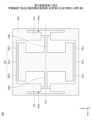
図10は、第2実施形態に係る可動装置である光偏向器の平面図(反射面側から視た図)である。図11は、第2実施形態に係る可動装置である光偏向器の底面図(反射面とは反対側から視た図)である。
Second Embodiment
Fig. 10 is a plan view (viewed from the reflecting surface side) of the optical deflector which is a movable device according to the second embodiment. Fig. 11 is a bottom view (viewed from the opposite side to the reflecting surface) of the optical deflector which is a movable device according to the second embodiment.

図10及び図11を参照すると、可動装置200は、両端支持構造の光偏向器である。可動装置200は、反射部202を含む可動部201をX軸に平行な第1軸AX1の周りに回動可能にする構造を備えている。すなわち、可動装置200は、反射部202を含む可動部201が1軸方向(第1軸AX1の周り)に回動することにより、入射する光を1軸方向に走査しながら偏向可能である。以下、可動装置200の構造について詳説する。Referring to Figures 10 and 11, themovable device 200 is an optical deflector with a support structure at both ends. Themovable device 200 has a structure that allows themovable part 201 including the reflectingpart 202 to rotate around a first axis AX1 parallel to the X-axis. In other words, themovable device 200 can deflect the incident light while scanning it in one axial direction by rotating themovable part 201 including the reflectingpart 202 in one axial direction (around the first axis AX1). The structure of themovable device 200 will be described in detail below.

可動装置200は、主に、可動部201と、反射部202と、駆動部203a及び203bと、支持部204と、一対のトーション梁220a及び220bとを有している。可動装置200は、例えば、可動部201の中心に対して点対称に形成することができる。Themovable device 200 mainly includes amovable section 201, a reflectingsection 202, drivingsections 203a and 203b, asupport section 204, and a pair oftorsion beams 220a and 220b. Themovable device 200 can be formed, for example, point-symmetrically with respect to the center of themovable section 201.

可動部201は、中央部201aと、延出部201b及び201cとを有する。中央部201aは、例えば、X方向の長さよりもY方向の長さが長い矩形状である。延出部201bは、中央部201aの+Y側端部の両側から第1軸AX1が伸びる方向に延出している。延出部201cは、中央部201aの-Y側端部の両側から第1軸AX1が伸びる方向に延出している。延出部201b及び201cは、例えば、Y方向の長さよりもX方向の長さが長い矩形状である。Themovable part 201 has acentral part 201a and extendingparts 201b and 201c. Thecentral part 201a is, for example, rectangular in shape with a length in the Y direction longer than its length in the X direction. The extendingpart 201b extends from both sides of the +Y side end of thecentral part 201a in the direction in which the first axis AX1 extends. The extendingpart 201c extends from both sides of the -Y side end of thecentral part 201a in the direction in which the first axis AX1 extends. The extendingparts 201b and 201c are, for example, rectangular in shape with a length in the X direction longer than its length in the Y direction.

図10の例では、延出部201b及び201cは第1軸AX1と平行である。しかし、これには限らず、延出部201b及び201cは第1軸AX1に対して傾斜していてもよい。また、図10の例では、延出部201b及び201cは一定幅である。しかし、これには限らず、延出部201b及び201cは部分的に幅が異なっていてもよい。In the example of FIG. 10, theextensions 201b and 201c are parallel to the first axis AX1. However, this is not limited, and theextensions 201b and 201c may be inclined with respect to the first axis AX1. Also, in the example of FIG. 10, theextensions 201b and 201c have a constant width. However, this is not limited, and theextensions 201b and 201c may have partially different widths.

反射部202は、可動部201上に形成されている。具体的には、反射部202は、中央部201aの+Z側の面の大部分に形成されている。反射部202は、延出部201b及び201cの一部又は全部に形成されてもよい。反射部202は、図10の例では矩形状であるが、円形状、楕円形状、又は他の複雑な形状であってもよい。反射部202は、例えば、アルミニウム、金、若しくは銀等を含む金属薄膜、又はその多層膜で構成される。反射面202aは、反射部202の+Z側の面である。Thereflective portion 202 is formed on themovable portion 201. Specifically, thereflective portion 202 is formed on most of the surface on the +Z side of thecentral portion 201a. Thereflective portion 202 may be formed on a part or all of theextension portions 201b and 201c. Thereflective portion 202 is rectangular in the example of FIG. 10, but may be circular, elliptical, or other complex shapes. Thereflective portion 202 is composed of, for example, a thin metal film containing aluminum, gold, silver, or the like, or a multilayer film thereof. Thereflective surface 202a is the surface on the +Z side of thereflective portion 202.

駆動部203a及び203bは、反射部202を含む可動部201を回動可能な状態で支持する1対のアクチュエータである。駆動部203a及び203bの各々は、振動梁となる梁部215と、梁部215の上面に形成された駆動素子219a及び219bとを有している。The drivingunits 203a and 203b are a pair of actuators that support themovable unit 201 including the reflectingunit 202 in a rotatable state. Each of the drivingunits 203a and 203b has abeam portion 215 that serves as a vibrating beam, and drivingelements 219a and 219b formed on the upper surface of thebeam portion 215.

梁部215は、長手方向をY方向に向けて配置され、両端が支持部204の内側に接続されている。駆動素子219a及び219bは、長手方向をY方向に向けた短冊状に形成されている。駆動素子219a及び219bは、例えば、第1軸AX1に対して線対称となるように配置される。駆動素子219a及び219bは、例えば、圧電素子である。Thebeam portion 215 is arranged with its longitudinal direction facing the Y direction, and both ends are connected to the inside of thesupport portion 204. The drivingelements 219a and 219b are formed in a rectangular shape with its longitudinal direction facing the Y direction. The drivingelements 219a and 219b are arranged, for example, so as to be linearly symmetrical with respect to the first axis AX1. The drivingelements 219a and 219b are, for example, piezoelectric elements.

支持部204は、例えば、可動部201を囲うように矩形枠状に形成されている。支持部204は、例えば、シリコン支持層、酸化シリコン層、及びシリコン活性層から構成される。なお、支持部204は、可動部201を完全に囲うように形成される必要はなく、例えば、図1における支持部104a及び104bのように分離して配置することも可能である。Thesupport section 204 is formed, for example, in a rectangular frame shape so as to surround themovable section 201. Thesupport section 204 is composed, for example, of a silicon support layer, a silicon oxide layer, and a silicon active layer. Note that thesupport section 204 does not need to be formed so as to completely surround themovable section 201, and it is also possible to arrange thesupport section 204 separately, for example, like thesupport sections 104a and 104b in FIG. 1.

トーション梁220a及び220bは、可動部201の中央部201aの長手方向の略中央部に一端が接続し、第1軸AX1方向にそれぞれ延びている。トーション梁220a及び220bは、反射部202を含む可動部201を第1軸AX1の周りに可動可能に支持する一対の弾性支持部である。トーション梁220a及び220bは、例えば、シリコン活性層から構成される。Thetorsion beams 220a and 220b each have one end connected to approximately the center in the longitudinal direction of thecentral portion 201a of themovable portion 201, and each extend in the direction of the first axis AX1. Thetorsion beams 220a and 220b are a pair of elastic support parts that movably support themovable portion 201 including the reflectingportion 202 around the first axis AX1. Thetorsion beams 220a and 220b are composed of, for example, a silicon active layer.

トーション梁220aの他端は、駆動部203aの梁部215の長手方向の略中央部に接続されている。トーション梁220bの他端は、駆動部203bの梁部215の長手方向の略中央部に接続されている。トーション梁220a及び220bの長手方向と梁部215の長手方向は垂直である。トーション梁220aの中心軸は、例えば、第1軸AX1となる。The other end of thetorsion beam 220a is connected to approximately the center in the longitudinal direction of thebeam portion 215 of thedriving unit 203a. The other end of thetorsion beam 220b is connected to approximately the center in the longitudinal direction of thebeam portion 215 of thedriving unit 203b. The longitudinal directions of thetorsion beams 220a and 220b are perpendicular to the longitudinal direction of thebeam portion 215. The central axis of thetorsion beam 220a is, for example, the first axis AX1.

このように、駆動部203a及び203bの各々の梁部215は、トーション梁220aの中心軸である第1軸AX1に対してY方向の両側に配置されている。そして、梁部215は、反射部202を含む可動部201とトーション梁220a及び220bとを、支持部204に対して両側から支持している。In this way, thebeam portions 215 of each of the drivingunits 203a and 203b are arranged on both sides in the Y direction with respect to the first axis AX1, which is the central axis of thetorsion beam 220a. Thebeam portions 215 support themovable unit 201 including the reflectingunit 202 and thetorsion beams 220a and 220b from both sides relative to thesupport portion 204.

可動装置200において、駆動素子219a及び219bは、例えば、駆動素子郡119a及び119bと同一構造である。可動装置200では、例えば、駆動素子219a及び219bの下部電極と上部電極との間にパルス波又は正弦波の電圧信号を印加すると、駆動素子219a及び219bは、その電歪特性によって梁部215の表面の面内方向において伸縮を繰り返す。梁部215の曲げ振動は、トーション梁220a及び220bで回転振動(捻り振動)に変換され、反射部202を含む可動部201が第1軸AX1の周りに回動する。In themovable device 200, the drivingelements 219a and 219b have the same structure as the drivingelement groups 119a and 119b, for example. In themovable device 200, when a pulse wave or sine wave voltage signal is applied between the lower and upper electrodes of the drivingelements 219a and 219b, the drivingelements 219a and 219b repeatedly expand and contract in the in-plane direction of the surface of thebeam portion 215 due to their electrostrictive properties. The bending vibration of thebeam portion 215 is converted into a rotational vibration (twisting vibration) by thetorsion beams 220a and 220b, and themovable portion 201 including the reflectingportion 202 rotates around the first axis AX1.

可動装置200は、例えば、可動装置100と同様に、SOI基板、Si基板、又はAl基板等を用いて形成できる。Themovable device 200 can be formed, for example, using an SOI substrate, a Si substrate, an Al substrate, or the like, similar to themovable device 100.

なお、反射部202を含む可動部201を第1軸AX1の周りに駆動可能であれば、各構成部の形状は実施形態の形状に限定されない。例えば、トーション梁220a及び220b並びに梁部215が曲率を有した形状を有していてもよい。In addition, as long as themovable part 201 including the reflectingpart 202 can be driven around the first axis AX1, the shape of each component is not limited to the shape of the embodiment. For example, thetorsion beams 220a and 220b and thebeam part 215 may have a shape with curvature.

このように、可動装置200において、可動部201は、第1軸AX1の方向に延出する延出部201b及び201cを有する。これにより、可動装置100の場合と同様に、重力の影響による反射部202の走査角の変化及び走査中心の変化を抑制可能である。可動装置200において、図5~図9と同様の変形を施してもよい。In this way, in themovable device 200, themovable part 201 hasextension parts 201b and 201c that extend in the direction of the first axis AX1. This makes it possible to suppress changes in the scanning angle and scanning center of the reflectingpart 202 due to the influence of gravity, as in the case of themovable device 100. Themovable device 200 may be modified in the same manner as in Figures 5 to 9.

図12は、第2実施形態の変形例1に係る可動装置である光偏向器の平面図(反射面側から視た図)である。図12に示す可動装置200Aは、反射面を有する可動部を回動させて、反射面へ入射する光を1軸方向(X軸に平行な第1軸AX1の周り)に偏向する片持ち構造の光偏向器である。Figure 12 is a plan view (viewed from the reflecting surface side) of an optical deflector, which is a movable device according to Variation 1 of the second embodiment. Themovable device 200A shown in Figure 12 is an optical deflector with a cantilever structure that rotates a movable part having a reflecting surface to deflect light incident on the reflecting surface in one axial direction (around a first axis AX1 parallel to the X-axis).

可動装置200Aは、可動装置200とは異なり片持ち構造であるため、駆動部203c及び203dのように、第1軸AX1の片側のみに駆動部が設けられている。Unlikemovable device 200,movable device 200A has a cantilever structure, and therefore has driving units on only one side of first axis AX1, such as drivingunits 203c and 203d.

可動装置200Aでは、可動装置200と同様に、梁部215の曲げ振動を、トーション梁220a及び220bで回転振動(捻り振動)に変換することで、反射部202を含む可動部201を第1軸AX1の周りに回動することができる。In themovable device 200A, similar to themovable device 200, the bending vibration of thebeam portion 215 is converted into rotational vibration (twisting vibration) by thetorsion beams 220a and 220b, so that themovable portion 201 including the reflectingportion 202 can rotate around the first axis AX1.

可動装置200Aのような片持ち構造の場合でも、可動部201が第1軸AX1の方向に延出する延出部201b及び201cを有することで、可動装置200の場合と同様に、重力の影響による反射部202の走査角の変化及び走査中心の変化を抑制可能である。可動装置200Aにおいて、図5~図9と同様の変形を施してもよい。Even in the case of a cantilever structure such as themovable device 200A, themovable part 201 hasextension parts 201b and 201c that extend in the direction of the first axis AX1, so that it is possible to suppress changes in the scanning angle and scanning center of the reflectingpart 202 due to the influence of gravity, as in the case of themovable device 200. Themovable device 200A may be modified in the same manner as in Figures 5 to 9.

〈第3実施形態〉
第3実施形態では、第1実施形態及び第2実施形態に係る可動装置を利用した2軸の光偏向器の例を示す。なお、本実施形態では、第1軸AX1を回動の中心とした光走査を副走査とし、第2軸AX2を回動の中心とした光走査を主走査とする。
Third Embodiment
The third embodiment shows an example of a two-axis optical deflector that uses the movable device according to the first and second embodiments. In this embodiment, optical scanning with the first axis AX1 as the center of rotation is defined as sub-scanning, and optical scanning with the second axis AX2 as the center of rotation is defined as main scanning.

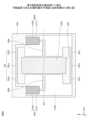
図13は、第3実施形態に係る可動装置である光偏向器の平面図(反射面側から視た図)である。Figure 13 is a plan view (viewed from the reflecting surface side) of an optical deflector, which is a movable device according to the third embodiment.

図13を参照すると、可動装置100Dは、両端支持構造の光偏向器である。可動装置100Dは、反射部202を含む可動部201及び可動部101をX軸に平行な第1軸AX1の周りに回動可能にする構造を備えている。また、可動装置100Dは、反射部202を含む可動部201をY軸に平行な第2軸AX2の周りに回動可能にする構造を備えている。すなわち、可動装置100Dは、反射部202を含む可動部201が2軸方向(第1軸AX1及び第2軸AX2の周り)に回動することにより、入射する光を2軸方向に走査しながら偏向可能である。Referring to FIG. 13, themovable device 100D is an optical deflector with a support structure at both ends. Themovable device 100D has a structure that allows themovable part 201 including the reflectingpart 202 and themovable part 101 to rotate around a first axis AX1 parallel to the X-axis. Themovable device 100D also has a structure that allows themovable part 201 including the reflectingpart 202 to rotate around a second axis AX2 parallel to the Y-axis. In other words, themovable device 100D can deflect the incident light while scanning it in two axial directions by rotating themovable part 201 including the reflectingpart 202 in two axial directions (around the first axis AX1 and the second axis AX2).

可動装置100Dは、可動装置100の中央部101aの内側に開口部を有し、開口部内に可動部201等を配置したものである。すなわち、開口部内には、可動装置200の支持部204の内側に相当する構造が配置されている。そして、可動部201は、第1軸AX1と直交する第2軸AX2を中心に回動可能に中央部101aに支持されている。なお、可動装置100Dは、可動装置200とは異なり、可動部201が延出部を有していない。可動装置100Dにおいて、梁部115の長手方向と、トーション梁220a及び220bの長手方向は、いずれもY方向(第2軸AX2の方向)を向いている。Themovable device 100D has an opening inside thecentral portion 101a of themovable device 100, and themovable portion 201 and the like are disposed inside the opening. That is, a structure equivalent to the inside of thesupport portion 204 of themovable device 200 is disposed inside the opening. Themovable portion 201 is supported by thecentral portion 101a so as to be rotatable about a second axis AX2 perpendicular to the first axis AX1. Note that, unlike themovable device 200, themovable portion 201 of themovable device 100D does not have an extension portion. In themovable device 100D, the longitudinal direction of thebeam portion 115 and the longitudinal directions of thetorsion beams 220a and 220b are all oriented in the Y direction (the direction of the second axis AX2).

可動装置100Dにおいて、可動装置100に相当する構造の部分が副走査方向の回動に寄与し、可動装置200に相当する構造の部分が主走査方向(高速軸)の回動に寄与する。すなわち、駆動部103a及び103bは、可動部201を含む可動部101を第1軸AX1回りに揺動させる。また、駆動部203a及び203bは、可動部201を第1軸AX1と直交する第2軸AX2周りに揺動させる。Inmovable device 100D, the structural portion corresponding tomovable device 100 contributes to rotation in the sub-scanning direction, and the structural portion corresponding tomovable device 200 contributes to rotation in the main scanning direction (high-speed axis). That is,drive units 103a and 103b oscillatemovable unit 101 includingmovable part 201 around first axis AX1.Drive units 203a and 203b also oscillatemovable part 201 around second axis AX2 that is perpendicular to first axis AX1.

このように、可動装置100Dにおいて、可動部101は、第1軸AX1の方向に延出する延出部101b及び101cを有する。これにより、可動装置100の場合と同様に、第1軸AX1の方向の回動に関し、重力の影響による反射部202の走査角の変化及び走査中心の変化を抑制可能である。可動装置100Dにおいて、図5~図9と同様の変形を施してもよい。In this way, in themovable device 100D, themovable part 101 hasextension parts 101b and 101c that extend in the direction of the first axis AX1. As a result, similar to the case of themovable device 100, it is possible to suppress changes in the scanning angle and scanning center of the reflectingpart 202 due to the influence of gravity in relation to rotation in the direction of the first axis AX1. In themovable device 100D, modifications similar to those shown in Figures 5 to 9 may be made.

図14は、第3実施形態の変形例1に係る可動装置である光偏向器の平面図(反射面側から視た図)である。図14に示す可動装置100Eは、可動部201が第2軸AX2の伸びる方向に延出する延出部201b及び201cを有する点が、可動装置100D(図13参照)と相違する。Figure 14 is a plan view (viewed from the reflecting surface side) of an optical deflector, which is a movable device according to Variation 1 of the third embodiment. Themovable device 100E shown in Figure 14 differs from themovable device 100D (see Figure 13) in that themovable part 201 hasextension parts 201b and 201c that extend in the direction in which the second axis AX2 extends.

可動装置100Eのように、可動部101が延出部101b及び101cを有し、さらに可動部201が延出部201b及び201cを有する構造であってもよい。これにより、可動装置100Dの場合と同様に、第1軸AX1の方向の回動に関し、重力の影響による反射部202の走査角の変化及び走査中心の変化を抑制可能である。そして、さらに第2軸AX2の方向の回動に関し、重力の影響による反射部202の走査角の変化及び走査中心の変化を抑制可能である。As inmovable device 100E,movable part 101 may haveextensions 101b and 101c, andmovable part 201 may haveextensions 201b and 201c. This makes it possible to suppress changes in the scanning angle and scanning center ofreflector 202 due to the influence of gravity when rotating in the direction of first axis AX1, as in the case ofmovable device 100D. Furthermore, it is possible to suppress changes in the scanning angle and scanning center ofreflector 202 due to the influence of gravity when rotating in the direction of second axis AX2.

以上に説明した第1~第3実施形態及び変形例に係る可動装置は、光走査システム、画像投影装置、光書込装置、及び物体認識装置に使用することができる。The movable devices according to the first to third embodiments and the modified examples described above can be used in optical scanning systems, image projection devices, optical writing devices, and object recognition devices.

[光走査システム]
まず、図15~図18を参照して、第1~第3実施形態及び変形例に係る可動装置のいずれかを搭載した光走査システムについて詳細に説明する。
[Optical scanning system]
First, an optical scanning system incorporating any one of the movable devices according to the first to third embodiments and the modified examples will be described in detail with reference to FIGS.

図15に、光走査システムの一例の概略図を示す。Figure 15 shows a schematic diagram of an example of an optical scanning system.

図15に示すように、光走査システム10は、駆動装置11の制御に従って光源装置12から照射された光を可動装置13の有する反射面14により偏向して被走査面15を光走査するシステムである。可動装置13は、第1~第3実施形態及び変形例に係る可動装置のいずれか1つである。As shown in FIG. 15, theoptical scanning system 10 is a system that deflects light irradiated from alight source device 12 by a reflectingsurface 14 of amovable device 13 under the control of a drivingdevice 11 to optically scan a scannedsurface 15. Themovable device 13 is any one of the movable devices according to the first to third embodiments and the modified examples.

光走査システム10は、駆動装置11、光源装置12、及び反射面14を有する可動装置13を含む。光走査システム10は、本発明に係る偏向装置の代表的な一例である。Theoptical scanning system 10 includes a drivingdevice 11, alight source device 12, and amovable device 13 having areflective surface 14. Theoptical scanning system 10 is a representative example of a deflection device according to the present invention.

駆動装置11は、例えばCPU(Central Processing Unit)及びFPGA(Field-Programmable Gate Array)等を備えた電子回路ユニットである。可動装置13は、例えば反射面14を有し、反射面14を可動可能なMEMS(Micro Electromechanical Systems)デバイスである。光源装置12は、例えばレーザを照射するレーザ装置である。なお、被走査面15は、例えばスクリーンである。The drivingdevice 11 is, for example, an electronic circuit unit equipped with a CPU (Central Processing Unit) and an FPGA (Field-Programmable Gate Array). Themovable device 13 is, for example, a MEMS (Micro Electromechanical Systems) device that has areflective surface 14 and can move thereflective surface 14. Thelight source device 12 is, for example, a laser device that irradiates a laser. The scannedsurface 15 is, for example, a screen.

駆動装置11は、取得した光走査情報に基づいて光源装置12及び可動装置13の制御命令を生成し、制御命令に基づいて光源装置12及び可動装置13に駆動信号を出力する。The drivingdevice 11 generates control commands for thelight source device 12 and themovable device 13 based on the acquired optical scanning information, and outputs driving signals to thelight source device 12 and themovable device 13 based on the control commands.

光源装置12は、入力された駆動信号に基づいて光源の照射を行う。可動装置13は、入力された駆動信号に基づいて反射面14を1軸方向又は2軸方向の少なくともいずれかに可動させる。Thelight source device 12 emits light based on the input drive signal. Themovable device 13 moves the reflectingsurface 14 in at least one axial direction or two axial directions based on the input drive signal.

これにより、駆動装置11は、例えば、光走査情報の一例である画像情報に基づいた制御によって、可動装置13の反射面14を所定の範囲で2軸方向に往復可動させ、反射面14に入射する光源装置12からの照射光を偏向して光走査する。その結果、駆動装置11は、被走査面15に任意の画像を投影することができる。As a result, the drivingdevice 11 moves the reflectingsurface 14 of themovable device 13 back and forth in two axial directions within a predetermined range by control based on image information, which is an example of optical scanning information, and deflects the irradiation light from thelight source device 12 that is incident on the reflectingsurface 14 to perform optical scanning. As a result, the drivingdevice 11 can project any image onto the scannedsurface 15.

なお、駆動装置11による制御の詳細については後述する。Details about the control by thedrive unit 11 will be described later.

次に、図16を参照して、光走査システム10の一例のハードウェア構成について説明する。Next, referring to FIG. 16, we will explain the hardware configuration of an example of theoptical scanning system 10.

図16は、光走査システム10の一例のハードウェア構成図である。Figure 16 is a hardware configuration diagram of an example of anoptical scanning system 10.

図16に示すように、光走査システム10は、駆動装置11、光源装置12及び可動装置13を備え、それぞれが電気的に接続されている。As shown in FIG. 16, theoptical scanning system 10 includes a drivingdevice 11, alight source device 12, and amovable device 13, each of which is electrically connected.

[駆動装置]
駆動装置11は、CPU20、RAM21(Random Access Memory)、ROM22(Read Only Memory)、FPGA23、外部I/F24、光源装置ドライバ25、及び光偏向器ドライバ26を備えている。
[Drive unit]
The drivingdevice 11 includes aCPU 20 , a RAM 21 (Random Access Memory), a ROM 22 (Read Only Memory), anFPGA 23 , an external I/F 24 , a lightsource device driver 25 , and anoptical deflector driver 26 .

CPU20は、ROM22等の記憶装置からプログラム又はデータをRAM21上に読み出し、処理を実行して、駆動装置11の全体の制御及び機能を実現する演算装置である。RAM21は、プログラム又はデータを一時保持する揮発性の記憶装置である。TheCPU 20 is a calculation device that reads programs or data from a storage device such as theROM 22 onto theRAM 21 and executes processing to realize the overall control and functions of thedrive device 11. TheRAM 21 is a volatile storage device that temporarily stores programs or data.

ROM22は、電源を切ってもプログラム又はデータを保持することができる不揮発性の記憶装置であり、CPU20が光走査システム10の各機能を制御するために実行する処理用プログラム又はデータを記憶している。TheROM 22 is a non-volatile storage device that can retain programs or data even when the power is turned off, and stores the processing programs or data that theCPU 20 executes to control each function of theoptical scanning system 10.

FPGA23は、CPU20の処理に従って、光源装置ドライバ25及び光偏向器ドライバ26に適した制御信号を出力する回路である。TheFPGA 23 is a circuit that outputs control signals suitable for the lightsource device driver 25 and theoptical deflector driver 26 according to the processing of theCPU 20.

外部I/F24は、例えば外部装置又はネットワーク等とのインタフェースである。外部装置には、例えば、PC(Personal Computer)等の上位装置、USBメモリ、SDカード、CD、DVD、HDD、又はSD等の記憶装置が含まれる。また、ネットワークは、例えば自動車のCAN(Controller Area Network)、LAN(Local Area Network)、又はンターネット等である。外部I/F24は、外部装置との接続又は通信を可能にする構成であればよく、外部装置ごとに外部I/F24が用意されてもよい。The external I/F 24 is, for example, an interface with an external device or a network. Examples of external devices include higher-level devices such as a PC (Personal Computer), and storage devices such as a USB memory, an SD card, a CD, a DVD, a HDD, or an SD. Examples of networks include an automobile's CAN (Controller Area Network), a LAN (Local Area Network), or the Internet. The external I/F 24 may have any configuration that enables connection or communication with an external device, and an external I/F 24 may be provided for each external device.

光源装置ドライバ25は、入力された制御信号に従って光源装置12に駆動電圧等の駆動信号を出力する電気回路である。The lightsource device driver 25 is an electrical circuit that outputs a drive signal, such as a drive voltage, to thelight source device 12 according to the input control signal.

光偏向器ドライバ26は、入力された制御信号に従って可動装置13に駆動電圧等の駆動信号を出力する電気回路である。Theoptical deflector driver 26 is an electrical circuit that outputs a drive signal, such as a drive voltage, to themovable device 13 according to the input control signal.

駆動装置11において、CPU20は、外部I/F24を介して外部装置又はネットワーク等から光走査情報を取得する。なお、駆動装置11は、CPU20が光走査情報を取得することができる構成であればよく、駆動装置11内のROM22又はFPGA23に光走査情報を格納する構成としてもよい。また、駆動装置11は、内部に新たにSSD等の記憶装置を設けて、その記憶装置に光走査情報を格納する構成としてもよい。In thedrive device 11, theCPU 20 acquires optical scanning information from an external device or a network via the external I/F 24. Thedrive device 11 may be configured to store the optical scanning information in theROM 22 orFPGA 23 within thedrive device 11 as long as theCPU 20 can acquire the optical scanning information. Thedrive device 11 may also be configured to store the optical scanning information in a new internal storage device such as an SSD.

ここで、光走査情報とは、被走査面15にどのように光走査させるかを示した情報であり、例えば、光走査により画像を表示する場合は、光走査情報は画像データである。また、例えば、光走査により光書込みを行う場合は、光走査情報は書込み順又は書込み箇所を示した書込みデータである。他にも、例えば、光走査により物体認識を行う場合は、光走査情報は物体認識用の光を照射するタイミングと照射範囲を示す照射データである。Here, the optical scanning information is information that indicates how to optically scan the scannedsurface 15. For example, when an image is displayed by optical scanning, the optical scanning information is image data. Also, for example, when optical writing is performed by optical scanning, the optical scanning information is writing data that indicates the writing order or writing location. In addition, for example, when object recognition is performed by optical scanning, the optical scanning information is irradiation data that indicates the timing and irradiation range of irradiating light for object recognition.

駆動装置11は、CPU20の命令及び図16に示したハードウェア構成によって、次に説明する機能構成を実現することができる。Thedrive device 11 can realize the functional configuration described below using instructions from theCPU 20 and the hardware configuration shown in FIG. 16.

[駆動装置の機能構成]
次に、図17を参照して、光走査システム10の駆動装置11の機能構成について説明する。図17は、光走査システムの駆動装置の一例の機能ブロック図である。
[Functional configuration of the driving device]
Next, a functional configuration of the drivingdevice 11 of theoptical scanning system 10 will be described with reference to Fig. 17. Fig. 17 is a functional block diagram of an example of the driving device of the optical scanning system.

図17に示すように、駆動装置11は、機能として制御部30と駆動信号出力部31とを有する。As shown in FIG. 17, thedrive device 11 has the functions of acontrol unit 30 and a drivesignal output unit 31.

制御部30は、例えばCPU20及びFPGA23等により実現され、外部装置から光走査情報を取得し、光走査情報を制御信号に変換して駆動信号出力部31に出力する。例えば、制御部30は、制御手段であり、外部装置等から画像データを光走査情報として取得し、所定の処理により画像データから制御信号を生成して駆動信号出力部31に出力する。Thecontrol unit 30 is realized by, for example, aCPU 20 and anFPGA 23, and acquires optical scanning information from an external device, converts the optical scanning information into a control signal, and outputs it to the drivesignal output unit 31. For example, thecontrol unit 30 is a control means, and acquires image data from an external device, etc. as optical scanning information, generates a control signal from the image data by performing a predetermined process, and outputs it to the drivesignal output unit 31.

駆動信号出力部31は、印加手段であり、光源装置ドライバ25及び光偏向器ドライバ26等により実現され、入力された制御信号に基づいて光源装置12又は可動装置13に駆動信号を出力する。駆動信号出力部31(印加手段)は、例えば、駆動信号を出力する対象ごとに設けられてもよい。The drivesignal output unit 31 is an application means, and is realized by the lightsource device driver 25 and theoptical deflector driver 26, etc., and outputs a drive signal to thelight source device 12 or themovable device 13 based on the input control signal. The drive signal output unit 31 (application means) may be provided, for example, for each target to which the drive signal is output.

駆動信号は、光源装置12又は可動装置13の駆動を制御するための信号である。例えば、光源装置12においては、駆動信号は、光源の照射タイミング及び照射強度を制御する駆動電圧である。また、例えば、可動装置13においては、駆動信号は、可動装置13の有する反射面14を可動させるタイミング及び可動範囲を制御する駆動電圧である。なお、駆動装置は、光源装置12又は受光装置等の外部装置から光源の照射タイミング及び受光タイミングを取得し、これらを可動装置13の駆動に同期するようにしてもよい。The drive signal is a signal for controlling the drive of thelight source device 12 or themovable device 13. For example, in thelight source device 12, the drive signal is a drive voltage that controls the timing and intensity of the light source irradiation. Also, for example, in themovable device 13, the drive signal is a drive voltage that controls the timing and range of movement of thereflective surface 14 of themovable device 13. The drive device may obtain the light source irradiation timing and light reception timing from an external device such as thelight source device 12 or a light receiving device, and synchronize these with the drive of themovable device 13.

[光走査処理]
次に、図18を参照して、光走査システム10が被走査面15を光走査する処理について説明する。図18は、光走査システムに係る処理の一例のフローチャートである。
[Optical scanning process]
Next, a process of optically scanning thesurface 15 to be scanned by theoptical scanning system 10 will be described with reference to Fig. 18. Fig. 18 is a flowchart of an example of a process related to the optical scanning system.

ステップS11において、制御部30は、外部装置等から光走査情報を取得する。In step S11, thecontrol unit 30 acquires optical scanning information from an external device, etc.

ステップS12において、制御部30は、取得した光走査情報から制御信号を生成し、制御信号を駆動信号出力部31に出力する。In step S12, thecontrol unit 30 generates a control signal from the acquired optical scanning information and outputs the control signal to the drivesignal output unit 31.

ステップS13において、駆動信号出力部31は、入力された制御信号に基づいて駆動信号を光源装置12及び可動装置13に出力する。In step S13, the drivesignal output unit 31 outputs a drive signal to thelight source device 12 and themovable device 13 based on the input control signal.

ステップS14において、光源装置12は、入力された駆動信号に基づいて光照射を行う。また、可動装置13は、入力された駆動信号に基づいて反射面14の可動を行う。光源装置12及び可動装置13の駆動により、反射面14に入射した光は任意の方向に偏向され、光走査される。In step S14, thelight source device 12 emits light based on the input drive signal. Themovable device 13 moves thereflective surface 14 based on the input drive signal. By driving thelight source device 12 and themovable device 13, the light incident on thereflective surface 14 is deflected in an arbitrary direction and optically scanned.

なお、上記光走査システム10では、1つの駆動装置11が光源装置12及び可動装置13を制御するが、光源装置12を制御する駆動装置と可動装置13を制御する駆動装置とを別々に設けてもよい。In theoptical scanning system 10, onedriving device 11 controls thelight source device 12 and themovable device 13, but a driving device that controls thelight source device 12 and a driving device that controls themovable device 13 may be provided separately.

また、上記光走査システム10では、一つの駆動装置11に制御部30の機能及び駆動信号出力部31の機能を設けている。しかし、これらの機能は別体として存在していてもよく、例えば制御部30を有した駆動装置11とは別に駆動信号出力部31を有した駆動信号出力装置を設けてもよい。なお、上記光走査システム10のうち、反射面14を有した可動装置13と駆動装置11により、光偏向を行う光偏向システムを構成してもよい。In addition, in theoptical scanning system 10, onedriving device 11 is provided with the functions of thecontrol unit 30 and the drivingsignal output unit 31. However, these functions may exist separately, for example, a driving signal output device having a drivingsignal output unit 31 may be provided separately from the drivingdevice 11 having thecontrol unit 30. Note that, in theoptical scanning system 10, themovable device 13 having thereflective surface 14 and the drivingdevice 11 may form an optical deflection system that performs optical deflection.

第1~第3実施形態及び変形例に係る可動装置のいずれかを光走査システムに用いることにより、重力の影響による可動装置の走査角の変化及び走査中心の変化が抑制されるため、高精度の光走査が可能となる。By using any of the movable devices according to the first to third embodiments and the modified examples in an optical scanning system, the change in the scanning angle and the scanning center of the movable device caused by the influence of gravity are suppressed, enabling optical scanning with high precision.

[画像投影装置]
次に、図19及び図20を参照して、可動装置13を適用した画像投影装置について詳細に説明する。
[Image Projection Device]
Next, an image projection device to which themovable device 13 is applied will be described in detail with reference to FIGS.

図19は、画像投影装置の一例であるヘッドアップディスプレイ装置500を搭載した自動車400の実施形態に係る概略図である。また、図20はヘッドアップディスプレイ装置500の一例の概略図である。Figure 19 is a schematic diagram of an embodiment of anautomobile 400 equipped with a head-updisplay device 500, which is an example of an image projection device. Also, Figure 20 is a schematic diagram of an example of the head-updisplay device 500.

画像投影装置は、光走査により画像を投影する装置であり、例えばヘッドアップディスプレイ装置である。An image projection device is a device that projects an image by optical scanning, such as a head-up display device.

図19に示すように、ヘッドアップディスプレイ装置500は、例えば、自動車400のウインドシールド(フロントガラス401等)の付近に設置される。ヘッドアップディスプレイ装置500から発せられる投射光Lがフロントガラス401で反射され、ユーザーである観察者(運転者402)に向かう。As shown in FIG. 19, the head-updisplay device 500 is installed, for example, near the windshield (windshield 401, etc.) of theautomobile 400. Projection light L emitted from the head-updisplay device 500 is reflected by thewindshield 401 and directed toward the observer (driver 402), who is the user.

これにより、運転者402は、ヘッドアップディスプレイ装置500によって投影された画像等を虚像として視認することができる。なお、ウインドシールドの内壁面にコンバイナを設置し、コンバイナによって反射する投射光によってユーザーに虚像を視認させる構成にしてもよい。This allows thedriver 402 to view the image projected by the head-updisplay device 500 as a virtual image. A combiner may be installed on the inner wall surface of the windshield, and the user may view a virtual image by projected light reflected by the combiner.

図20に示すように、ヘッドアップディスプレイ装置500は、赤色、緑色、及び青色のレーザ光源501R,501G,及び501Bからレーザ光が出射される。出射されたレーザ光は、各レーザ光源に対して設けられるコリメートレンズ502,503,及び504と、2つのダイクロイックミラー505及び506と、光量調整部507とを含む入射光学系に入射する。そして、入射光学系を経たレーザ光は、反射面14を有する可動装置13で偏向される。As shown in FIG. 20, in the head-updisplay device 500, laser light is emitted from red, green, and bluelaser light sources 501R, 501G, and 501B. The emitted laser light is incident on an incident optical system includingcollimator lenses 502, 503, and 504 provided for each laser light source, twodichroic mirrors 505 and 506, and a lightamount adjustment unit 507. The laser light that passes through the incident optical system is deflected by amovable device 13 having a reflectingsurface 14.

そして、偏向されたレーザ光は、自由曲面ミラー509と、中間スクリーン510と、投射ミラー511とを含む投射光学系を経て、スクリーンに投影される。The deflected laser light then passes through a projection optical system that includes a free-form surface mirror 509, anintermediate screen 510, and aprojection mirror 511, and is projected onto the screen.

ヘッドアップディスプレイ装置500では、レーザ光源501R,501G,及び501B、コリメートレンズ502,503,及び504、並びにダイクロイックミラー505及び506は、光源ユニット530として光学ハウジングでユニット化されている。In the head-updisplay device 500, thelaser light sources 501R, 501G, and 501B, thecollimating lenses 502, 503, and 504, and thedichroic mirrors 505 and 506 are unitized in an optical housing as thelight source unit 530.

上記ヘッドアップディスプレイ装置500は、中間スクリーン510に表示される中間像を自動車400のフロントガラス401に投射することで、その中間像を運転者402に虚像として視認させる。The head-updisplay device 500 projects an intermediate image displayed on anintermediate screen 510 onto thewindshield 401 of theautomobile 400, allowing thedriver 402 to view the intermediate image as a virtual image.

レーザ光源501R,501G,及び501Bから発せられる各色レーザ光は、それぞれ、コリメートレンズ502,503,及び504で略平行光とされ、2つのダイクロイックミラー505及び506により合成される。合成されたレーザ光は、光量調整部507で光量が調整された後、反射面14を有する可動装置13によって二次元走査される。可動装置13で二次元走査された投射光Lは、自由曲面ミラー509で反射されて歪みを補正された後、中間スクリーン510に集光され、中間像を表示する。中間スクリーン510は、例えば、マイクロレンズが二次元配置されたマイクロレンズアレイであり、中間スクリーン510に入射する投射光Lをマイクロレンズ単位で拡大する。The laser light of each color emitted from thelaser light sources 501R, 501G, and 501B is converted into approximately parallel light by thecollimating lenses 502, 503, and 504, respectively, and is combined by the twodichroic mirrors 505 and 506. The combined laser light is adjusted in light amount by the lightamount adjustment unit 507, and then scanned two-dimensionally by themovable device 13 having the reflectingsurface 14. The projection light L scanned two-dimensionally by themovable device 13 is reflected by the free-form surface mirror 509, where distortion is corrected, and then focused on theintermediate screen 510 to display an intermediate image. Theintermediate screen 510 is, for example, a microlens array in which microlenses are arranged two-dimensionally, and the projection light L incident on theintermediate screen 510 is magnified in microlens units.

可動装置13は、反射面14を2軸方向に往復可動させ、反射面14に入射する投射光Lを二次元走査する。可動装置13の反射面14は、レーザ光源501R,501G,及び501Bの発光タイミングに同期して制御される。Themovable device 13 reciprocates thereflective surface 14 in two axial directions, two-dimensionally scanning the projection light L incident on thereflective surface 14. Thereflective surface 14 of themovable device 13 is controlled in synchronization with the emission timing of thelaser light sources 501R, 501G, and 501B.

以上、画像投影装置の一例としてのヘッドアップディスプレイ装置500の説明をしたが、画像投影装置は、反射面14を有した可動装置13により光走査を行うことで画像を投影する装置であれば、ヘッドアップディスプレイ装置以外であってもよい。The above describes the head-updisplay device 500 as an example of an image projection device, but the image projection device may be a device other than a head-up display device as long as it projects an image by performing optical scanning using amovable device 13 having areflective surface 14.

画像投影装置は、例えば、机等に置かれ、表示スクリーン上に画像を投影するプロジェクタにも、同様に適用することができる。また、画像投影装置は、観測者の頭部等に装着される装着部材に搭載され、装着部材が有する反射透過スクリーンに投影、又は眼球をスクリーンとして画像を投影するヘッドマウントディスプレイ装置等にも、同様に適用することができる。The image projection device can be similarly applied to, for example, a projector that is placed on a desk or the like and projects an image onto a display screen. The image projection device can also be similarly applied to a head-mounted display device that is mounted on a mounting member that is worn on the observer's head or the like and projects an image onto a reflective/transmissive screen that the mounting member has, or projects an image using the eyeball as a screen.

また、画像投影装置は、車両又は装着部材だけでなく、例えば、航空機、船舶、及び移動式ロボット等の移動体、あるいは、その場から移動せずにマニピュレータ等の駆動対象を操作する作業ロボットなどの非移動体に搭載されてもよい。The image projection device may be mounted not only on a vehicle or a mounting member, but also on a moving body such as an aircraft, a ship, or a mobile robot, or on a non-moving body such as a work robot that operates a drive target such as a manipulator without moving from its location.

第1~第3実施形態及び変形例に係る可動装置のいずれかを画像投影装置に用いることにより、重力の影響による可動装置の走査角の変化及び走査中心の変化が抑制されるため、高精度の画像投影が可能となる。By using any of the movable devices according to the first to third embodiments and the modified examples in an image projection device, changes in the scanning angle and scanning center of the movable device caused by the influence of gravity are suppressed, enabling highly accurate image projection.

[光書込装置]
次に、図21及び図22を参照して、可動装置13を適用した光書込装置について詳細に説明する。
[Optical writing device]
Next, an optical writing device to which themovable device 13 is applied will be described in detail with reference to FIGS.

図21は、光書込装置600を組み込んだ画像形成装置の一例である。また、図22は、光書込装置の一例の概略図である。Figure 21 shows an example of an image forming device incorporating anoptical writing device 600. Figure 22 is a schematic diagram of an example of an optical writing device.

図21に示すように、上記光書込装置600は、レーザ光によるプリンタ機能を有するレーザプリンタ650等に代表される画像形成装置の構成部材として使用される。画像形成装置において光書込装置600は、1本又は複数本のレーザビームで被走査面15である感光体ドラムを光走査することにより、感光体ドラムに光書込を行う。As shown in FIG. 21, theoptical writing device 600 is used as a component of an image forming device such as alaser printer 650 having a printer function using laser light. In the image forming device, theoptical writing device 600 optically writes on the photosensitive drum, which is the scannedsurface 15, by optically scanning the photosensitive drum with one or more laser beams.

図22に示すように、光書込装置600において、レーザ素子などの光源装置12からのレーザ光は、コリメートレンズなどの結像光学系601を経た後、反射面14を有する可動装置13により1軸方向又は2軸方向に偏向される。As shown in FIG. 22, in anoptical writing device 600, laser light from alight source device 12 such as a laser element passes through an imagingoptical system 601 such as a collimator lens, and is then deflected in one or two axial directions by amovable device 13 having areflective surface 14.

そして、可動装置13で偏向されたレーザ光は、その後、第一レンズ602aと第二レンズ602b、及び反射ミラー部602cを含む走査光学系602を経て、被走査面15(例えば感光体ドラム又は感光紙)に照射し、光書込みを行う。走査光学系602は、被走査面15にスポット状に光ビームを結像する。The laser light deflected by themovable device 13 then passes through the scanningoptical system 602, which includes afirst lens 602a, asecond lens 602b, and a reflectingmirror portion 602c, and is irradiated onto the surface to be scanned 15 (e.g., a photosensitive drum or photosensitive paper) to perform optical writing. The scanningoptical system 602 forms a spot-shaped light beam on the surface to be scanned 15.

また、光源装置12及び反射面14を有する可動装置13は、駆動装置11の制御に基づき駆動する。In addition, thelight source device 12 and themovable device 13 having thereflective surface 14 are driven based on the control of the drivingdevice 11.

このように上記光書込装置600は、レーザ光によるプリンタ機能を有する画像形成装置の構成部材として使用することができる。In this way, theoptical writing device 600 can be used as a component of an image forming device that has a laser light printer function.

また、光書込装置600は、走査光学系を異ならせて1軸方向だけでなく2軸方向に光走査することも可能である。光書込装置600は、例えば、レーザ光をサーマルメディアに偏向して2軸方向に光走査し、サーマルメディアを加熱することで印字するレーザラベル装置等の画像形成装置の構成部材として使用することができる。Theoptical writing device 600 can also perform optical scanning in not only one axis direction but also two axes directions by changing the scanning optical system. Theoptical writing device 600 can be used, for example, as a component of an image forming device such as a laser label device that deflects laser light onto thermal media to perform optical scanning in two axes directions and prints by heating the thermal media.

上記光書込装置に適用される反射面14を有した可動装置13は、ポリゴンミラー等を用いた回転多面鏡に比べ駆動のための消費電力が小さいため、光書込装置の省電力化に有利である。Themovable device 13 having areflective surface 14 used in the optical writing device described above consumes less power to operate than a rotating polygon mirror using a polygon mirror or the like, and is therefore advantageous in reducing the power consumption of the optical writing device.

また、可動装置13の振動時における風切り音は回転多面鏡に比べ小さいため、光書込装置の静粛性の改善に有利である。光書込装置は回転多面鏡に比べ設置スペースが圧倒的に少なくて済み、また可動装置13の発熱量もわずかであるため、小型化が容易であり、よって画像形成装置の小型化に有利である。In addition, the wind noise generated by themovable device 13 when it vibrates is smaller than that of a rotating polygon mirror, which is advantageous for improving the quietness of the optical writing device. The optical writing device requires an overwhelmingly smaller installation space than a rotating polygon mirror, and themovable device 13 generates only a small amount of heat, making it easy to miniaturize the device, which is advantageous for miniaturizing the image forming device.

第1~第3実施形態及び変形例に係る可動装置のいずれかを光書込装置に用いることにより、重力の影響による可動装置の走査角の変化及び走査中心の変化が抑制されるため、高精度の光書き込みが可能となる。By using any of the movable devices according to the first to third embodiments and the modified examples in an optical writing device, the change in the scanning angle and the scanning center of the movable device caused by the influence of gravity are suppressed, making it possible to perform optical writing with high precision.

[物体認識装置]
次に、図23及び図24を参照して、可動装置13を適用した物体認識装置について詳細に説明する。
[Object Recognition Device]
Next, an object recognition device to which themovable device 13 is applied will be described in detail with reference to FIGS.

図23は、物体認識装置の一例であるレーザレーダ装置を搭載した自動車の概略図である。また、図24はレーザレーダ装置の一例の概略図である。Figure 23 is a schematic diagram of an automobile equipped with a laser radar device, which is an example of an object recognition device. Also, Figure 24 is a schematic diagram of an example of a laser radar device.

物体認識装置は、対象方向の物体を認識する装置であり、例えばレーザレーダ装置である。An object recognition device is a device that recognizes objects in a target direction, such as a laser radar device.

図23に示すように、レーザレーダ装置700は、例えば自動車701に搭載され、対象方向を光走査して、対象方向に存在する被対象物702からの反射光を受光することで、被対象物702を認識する。As shown in FIG. 23, thelaser radar device 700 is mounted on, for example, anautomobile 701, and recognizes anobject 702 by optically scanning the target direction and receiving reflected light from theobject 702 present in the target direction.

図24に示すように、光源装置12から出射されたレーザ光は、発散光を略平行光とする光学系であるコリメートレンズ703と、平面ミラー704とを含む入射光学系を経て、反射面14を有する可動装置13で1軸もしくは2軸方向に走査される。As shown in FIG. 24, the laser light emitted from thelight source device 12 passes through an incident optical system including acollimating lens 703, which is an optical system that converts divergent light into approximately parallel light, and aplane mirror 704, and is scanned in one or two axial directions by amovable device 13 having areflective surface 14.

そして、2軸方向に走査されたレーザ光は、投光光学系である投光レンズ705等を経て装置前方の被対象物702に照射される。光源装置12及び可動装置13は、駆動装置11により駆動を制御される。被対象物702で反射された反射光は、光検出器709により光検出される。The laser light scanned in two axial directions is then irradiated onto theobject 702 in front of the device via aprojection lens 705, which is a projection optical system. Thelight source device 12 and themovable device 13 are controlled by a drivingdevice 11. The light reflected by theobject 702 is optically detected by aphotodetector 709.

すなわち、被対象物702で反射された反射光は受光光学系である集光レンズ706等を経て撮像素子707により受光され、撮像素子707は検出信号を信号処理回路708に出力する。信号処理回路708は、入力された検出信号に2値化又はノイズ処理等の所定の処理を行い、結果を測距回路710に出力する。That is, the light reflected by theobject 702 passes through the light receiving optical system, such as thecondenser lens 706, and is received by theimage sensor 707, which outputs a detection signal to thesignal processing circuit 708. Thesignal processing circuit 708 performs predetermined processing, such as binarization or noise processing, on the input detection signal, and outputs the result to thedistance measurement circuit 710.

測距回路710は、光源装置12がレーザ光を発光したタイミングと、光検出器709でレーザ光を受光したタイミングとの時間差、又は受光した撮像素子707の画素ごとの位相差とによって、被対象物702の有無を認識する。測距回路710は、さらに被対象物702との距離情報を算出する。Thedistance measurement circuit 710 recognizes the presence or absence of theobject 702 based on the time difference between when thelight source device 12 emits the laser light and when thephotodetector 709 receives the laser light, or the phase difference between each pixel of theimage sensor 707 that receives the light. Thedistance measurement circuit 710 further calculates distance information to theobject 702.

反射面14を有する可動装置13は多面鏡に比べて破損しづらく、小型であるため、耐久性の高い小型のレーダ装置を提供することができる。Themovable device 13 with thereflective surface 14 is less prone to breakage than a polygonal mirror and is small, making it possible to provide a small, highly durable radar device.

このようなレーザレーダ装置は、例えば、車両、航空機、船舶及び移動式ロボット等の移動体、あるいは、その場から移動せずにマニピュレータ等の駆動対象を操作する作業ロボットなどの非移動体に搭載できる。そして、レーザレーダ装置は、所定範囲を光走査して障害物の有無又は障害物までの距離を認識することができる。Such a laser radar device can be mounted on moving bodies such as vehicles, aircraft, ships, and mobile robots, or on non-moving bodies such as work robots that operate drive objects such as manipulators without moving from their locations. The laser radar device can optically scan a specified range to determine the presence or absence of obstacles and the distance to the obstacles.

なお、上記では、物体認識装置の一例として、レーザレーダ装置700の説明をしたが、物体認識装置はレーザレーダ装置に限定されるものではない。物体認識装置は、反射面14を有した可動装置13を駆動装置11で制御することにより光走査を行い、光検出器により反射光を受光することで被対象物702を認識する装置であれば、レーザレーダ装置以外であってもよい。In the above, thelaser radar device 700 has been described as an example of an object recognition device, but the object recognition device is not limited to a laser radar device. The object recognition device may be a device other than a laser radar device, so long as it performs optical scanning by controlling amovable device 13 having areflective surface 14 with a drivingdevice 11, and recognizes thetarget object 702 by receiving reflected light with a photodetector.

物体認識装置は、例えば、手又は顔を光走査して得た距離情報から形状等の物体情報を算出し、記録と参照することで対象物を認識する生体認証にも同様に適用することができる。また、物体認識装置は、対象範囲への光走査により侵入物を認識するセキュリティセンサ、及び光走査により得た距離情報から形状等の物体情報を算出して認識し、3次元データとして出力する3次元スキャナの構成部材などにも同様に適用することができる。The object recognition device can be similarly applied to biometric authentication, for example, where object information such as shape is calculated from distance information obtained by optically scanning a hand or face, and the target object is recognized by referring to a record. The object recognition device can also be similarly applied to security sensors that recognize intruding objects by optically scanning a target range, and to components of three-dimensional scanners that calculate and recognize object information such as shape from distance information obtained by optical scanning, and output it as three-dimensional data.

第1~第3実施形態及び変形例に係る可動装置のいずれかを物体認識装置に用いることにより、重力の影響による可動装置の走査角の変化及び走査中心の変化が抑制されるため、高精度の物体認識が可能となる。By using any of the movable devices according to the first to third embodiments and the modified examples in an object recognition device, changes in the scanning angle and scanning center of the movable device caused by the influence of gravity are suppressed, making it possible to recognize objects with high accuracy.
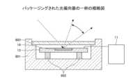
[パッケージング]
次に、図25を参照して、光偏向器である可動装置13のパッケージングについて説明する。
[Packaging]
Next, with reference to FIG. 25, packaging of themovable device 13, which is an optical deflector, will be described.

図25は、パッケージングされた光偏向器の一例の概略図である。Figure 25 is a schematic diagram of an example of a packaged optical deflector.

図25に示すように、可動装置13は、凹状のパッケージ部材801の底面に配置される取付部材802に取り付けられている。パッケージ部材801には、可動装置13が配置された領域を覆う透過部材803が設けられている。パッケージ部材801と透過部材803で密閉されることで、可動装置13がパッケージングされる。As shown in FIG. 25, themovable device 13 is attached to anattachment member 802 that is disposed on the bottom surface of aconcave packaging member 801. Thepackaging member 801 is provided with atransparent member 803 that covers the area in which themovable device 13 is disposed. Themovable device 13 is packaged by being sealed between thepackaging member 801 and thetransparent member 803.

さらに、パッケージ内は窒素等の不活性ガスが密封されている。これにより、可動装置13の酸化による劣化が抑制され、さらに温度等の環境の変化に対する耐久性が向上する。In addition, an inert gas such as nitrogen is sealed inside the package. This prevents themovable device 13 from deteriorating due to oxidation, and improves its durability against environmental changes such as temperature.

以上、好ましい実施形態等について詳説したが、上述した実施形態等に制限されることはなく、特許請求の範囲に記載された範囲を逸脱することなく、上述した実施形態等に種々の変形及び置換を加えることができる。Although the preferred embodiments have been described above in detail, the present invention is not limited to the above-described embodiments, and various modifications and substitutions can be made to the above-described embodiments without departing from the scope of the claims.

例えば、上記の各実施形態において、可動部を揺動させる駆動手段に圧電素子を用いた圧電駆動方式を用いる例を示したが、これには限定されず、例えば静電力を利用して駆動する静電駆動方式、又は電磁力を利用して駆動する電磁駆動方式を用いてもよい。又、第3実施形態において、主走査方向に可動部を揺動させる駆動手段、副走査方向に可動部を揺動させる駆動手段としていずれも同じ駆動方式を採用しているが、これらは互いに異なる駆動方式を採用してもよい。For example, in each of the above embodiments, an example has been shown in which a piezoelectric driving method using a piezoelectric element is used as the driving means for oscillating the movable part, but this is not limited to this, and for example, an electrostatic driving method that uses electrostatic force for driving, or an electromagnetic driving method that uses electromagnetic force for driving, may also be used. Also, in the third embodiment, the same driving method is used as the driving means for oscillating the movable part in the main scanning direction and the driving means for oscillating the movable part in the sub-scanning direction, but different driving methods may also be used.

また、上記の各実施形態では可動部が反射部を有しているが、可動部は反射部の代わりに回折格子、フォトダイオード、ヒータ(例えば、SiNを用いたヒータ)、光源(例えば、面発光型レーザ)等を有してもよい。In addition, in each of the above embodiments, the movable part has a reflecting part, but the movable part may have a diffraction grating, a photodiode, a heater (e.g., a heater using SiN), a light source (e.g., a surface-emitting laser), etc. instead of a reflecting part.

10 光走査システム
12 光源装置
13 可動装置
14 反射面
15 被走査面
20 CPU
21 RAM
22 ROM
23 FPGA
24 外部I/F
25 光源装置ドライバ
26 光偏向器ドライバ
30 制御部
31 駆動信号出力部
100,100A,100B,100C,100D,100E,200,200A 可動装置
101,201 可動部
101a,201a 中央部
101b,101c,201b,201c 延出部
101d,101e,101f,101g 突出部
102,202 反射部
102a,202a 反射面
103a,103b,203a,203b,203c,203d 駆動部
104a,104b,204 支持部
108 突起部
115,215 梁部
116 接続部
117a,117b 可動部接続部
118a,118b 支持部接続部
119a,119b 駆動素子郡
131 シリコン支持層
132 酸化シリコン層
133 シリコン活性層
135 下部電極
136 圧電部
137 上部電極
219a,219b駆動素子
220a,220b トーション梁
400 自動車
401 フロントガラス
402 運転者
500 ヘッドアップディスプレイ装置
501R,501G,501B レーザ光源
502,503,504 コリメートレンズ
505,506 ダイクロイックミラー
507 光量調整部
509 自由曲面ミラー
510 中間スクリーン
511 投射ミラー
530 光源ユニット
600 光書込装置
601 結像光学系
602 走査光学系
602a 第一レンズ
602b 第二レンズ
602c 反射ミラー部
650 レーザプリンタ
700 レーザレーダ装置
701 自動車
702 被対象物
703 コリメートレンズ
704 平面ミラー
705 投光レンズ
706 集光レンズ
707 撮像素子
708 信号処理回路
709 光検出器
710 測距回路
801 パッケージ部材
802 取付部材
803 透過部材
10Optical scanning system 12Light source device 13Movable device 14 Reflectingsurface 15 Scannedsurface 20 CPU
21 RAM
22 ROM
23 FPGA
24 External I/F
25 Light source device driver 26 Optical deflector driver 30 Control section 31 Drive signal output section 100, 100A, 100B, 100C, 100D, 100E, 200, 200A Movable device 101, 201 Movable section 101a, 201a Central section 101b, 101c, 201b, 201c Extension parts 101d, 101e, 101f, 101g Projection parts 102, 202 Reflection parts 102a, 202a Reflection surfaces 103a, 103b, 203a, 203b, 203c, 203d Drive parts 104a, 104b, 204 Support part 108 Projection parts 115, 215 Beam part 116 Connection parts 117a, 117b Movable part connection parts 118a, 118b Support part connection parts 119a, 119b Drive element group 131 Silicon support layer 132 Silicon oxide layer 133 Silicon active layer 135 Lower electrode 136 Piezoelectric part 137 Upper electrodes 219a, 219b Drive elements 220a, 220b Torsion beam 400 Automobile 401 Windshield 402 Driver 500 Head-up display device 501R, 501G, 501B Laser light source 502, 503, 504 Collimator lenses 505, 506 Dichroic mirror 507 Light amount adjustment part 509 Free-form surface mirror 510 Intermediate screen 511 Projection mirror 530 Light source unit 600 Optical writing device 601 Imaging optical system 602 Scanning optical system 602a First lens 602b Second lens 602c Reflecting mirror section 650 Laser printer 700 Laser radar device 701 Automobile 702 Object 703 Collimating lens 704 Plane mirror 705 Light projecting lens 706 Condenser lens 707 Image pickup element 708 Signal processing circuit 709 Photodetector 710 Distance measurement circuit 801 Package member 802 Mounting member 803 Transmissive member

特開2020-003531号公報JP 2020-003531 A

Claims (16)

Translated fromJapanese
所定の軸を中心に回動可能な可動部と、
前記可動部に一端が接続され、前記可動部を回動させる駆動部と、を備え、
前記可動部は、前記所定の軸が伸びる方向に延出する延出部を有し、
平面視で、前記可動部は、前記延出部の長手方向の端部に、前記駆動部とは反対側に突出する突出部を有する、可動装置。
A movable part that is rotatable around a predetermined axis;
a drive unit connected to the movable unit at one end and configured to rotate the movable unit,
The movable portionhas an extension portion extending in a direction in which the predetermined axis extends,
A movable device, wherein, in a plan view, the movable portion has a protrusion at a longitudinal end of the extension portion that protrudes on the side opposite the drive portion .
所定の軸を中心に回動可能な可動部と、
前記可動部に一端が接続され、前記可動部を回動させる駆動部と、を備え、
前記可動部は、前記所定の軸が伸びる方向に延出する延出部を有し、
平面視で、前記可動部は、前記延出部の長手方向の端部に、前記駆動部の側に突出する突出部を有する、可動装置。
A movable part that is rotatable around a predetermined axis;
a drive unit connected to the movable unit at one end and configured to rotate the movable unit,
The movable portionhas an extension portion extending in a direction in which the predetermined axis extends,
A movable device, wherein, in a plan view, the movable portion has a protrusion at a longitudinal end of the extension portion that protrudes toward the drive portion .
前記延出部は、長手方向が前記所定の軸と平行である、請求項1又は2に記載の可動装置。 The movable device according to claim 1or 2 , wherein the extension portion has a longitudinal direction parallel to the predetermined axis. 前記延出部は、厚さ方向の一方側に突起する突起部を有する、請求項1乃至3のいずれか一項に記載の可動装置。 The movable deviceaccording to claim 1 , wherein the extension portion has a protrusion that protrudes to one side in a thickness direction. 前記駆動部は、複数の梁部が接続部により接続されたミアンダ構造である、請求項1乃至のいずれか一項に記載の可動装置。 The movable device according to claim1 , wherein the driving section has a meandering structure in which a plurality of beam sections are connected by connecting sections. 一端が前記可動部の両側に接続し、他端が前記駆動部に接続する一対のトーション梁を有する、請求項1乃至のいずれか一項に記載の可動装置。 The movable device according to claim1 , further comprising a pair of torsion beams, one end of which is connected to either side of the movable part and the other end of which is connected to the driving part. 前記可動部は、前記所定の軸に対して、平面形状及び質量が対称である、請求項1乃至のいずれか一項に記載の可動装置。 The movable device according to claim1 , wherein the movable portion has a planar shape and a mass that are symmetrical with respect to the predetermined axis. 前記可動部は、前記所定の軸を跨ぐように配置された中央部を有し、
前記延出部は、前記中央部の前記所定の軸に直交する方向の一端部の両側から前記所定の軸が伸びる方向に延出する第1延出部と、前記中央部の前記所定の軸に直交する方向の他端部の両側から前記所定の軸が伸びる方向に延出する第2延出部と、を含む、請求項1乃至のいずれか一項に記載の可動装置。
the movable portion has a central portion disposed so as to straddle the predetermined axis,
The movable device according to any one of claims 1 to 7, wherein the extension portion includes a first extension portion extending in the direction in which the specified axis extends from both sides of one end of the central portion in a direction perpendicular to the specified axis, and a second extension portion extending in the direction in which the specified axis extends from both sides of the other end of the central portion in a direction perpendicular to the specifiedaxis .
前記中央部の一方の面には、反射部が設けられている、請求項に記載の可動装置。 The movable device according to claim8 , wherein a reflecting portion is provided on one surface of the central portion. 前記中央部、前記第1延出部、及び前記第2延出部のそれぞれの一方の面の全面に、前記反射部が設けられている、請求項に記載の可動装置。 The movable device according to claim9 , wherein the reflecting portion is provided on an entire surface of one surface of each of the central portion, the first extending portion, and the second extending portion. 前記中央部は、開口部を有し、
前記開口部の内側には、第2可動部が配置され、
前記第2可動部は、前記所定の軸と直交する他の軸を中心に回動可能に前記中央部に支持されている、請求項乃至10のいずれか一項に記載の可動装置。
The central portion has an opening,
A second movable part is disposed inside the opening,
The movable device according to claim8, wherein the second movable portion is supported by the central portion so as to be rotatable about another axis perpendicular to the predetermined axis.
前記第2可動部は、前記他の軸が伸びる方向に延出する延出部を有する、請求項11に記載の可動装置。 The movable device according to claim11 , wherein the second movable portion has an extension portion that extends in a direction in which the other axis extends. 請求項1乃至12のいずれか一項に記載の可動装置と、
光源と、
を備えた偏向装置。
A movable device according to any one of claims 1 to12 ,
A light source;
A deflection device comprising:
請求項1乃至12のいずれか一項に記載の可動装置を備える物体認識装置。 An object recognition device comprising a movable device according to any one of claims 1 to12 . 請求項1乃至12のいずれか一項に記載の可動装置を備える画像投影装置。 An image projection device comprising a movable device according to any one of claims 1 to12 . 請求項14に記載の物体認識装置、請求項15に記載の画像投影装置の少なくとも1つを有する移動体。 A moving body comprising at least one of the object recognition device according to claim14 and the image projection device according to claim15 .
JP2021047767A2021-03-222021-03-22 Movable device, deflection device, object recognition device, image projection device, and moving bodyActiveJP7608909B2 (en)

Priority Applications (1)

Application NumberPriority DateFiling DateTitle
JP2021047767AJP7608909B2 (en)2021-03-222021-03-22 Movable device, deflection device, object recognition device, image projection device, and moving body

Applications Claiming Priority (1)

Application NumberPriority DateFiling DateTitle
JP2021047767AJP7608909B2 (en)2021-03-222021-03-22 Movable device, deflection device, object recognition device, image projection device, and moving body

Publications (2)

Publication NumberPublication Date
JP2022146675A JP2022146675A (en)2022-10-05
JP7608909B2true JP7608909B2 (en)2025-01-07

Family

ID=83461616

Family Applications (1)

Application NumberTitlePriority DateFiling Date
JP2021047767AActiveJP7608909B2 (en)2021-03-222021-03-22 Movable device, deflection device, object recognition device, image projection device, and moving body

Country Status (1)

CountryLink
JP (1)JP7608909B2 (en)

Citations (7)

* Cited by examiner, † Cited by third party
Publication numberPriority datePublication dateAssigneeTitle
JP2003084226A (en)2001-09-142003-03-19Ricoh Co Ltd Optical scanning device
JP2005099186A (en)2003-09-222005-04-14Fuji Photo Film Co LtdOptical modulation device, optical modulation array device and exposure apparatus using the same
JP2010002637A (en)2008-06-192010-01-07Canon Electronics IncOptical scanning apparatus
JP2011095290A (en)2009-10-272011-05-12Seiko Epson CorpOptical deflection element, optical deflector and image forming apparatus
WO2014122781A1 (en)2013-02-082014-08-14パイオニア株式会社Actuator
JP2018155989A (en)2017-03-212018-10-04株式会社リコーOptical scan system, image projection device, and object recognition device
US20200057298A1 (en)2018-08-142020-02-20Stmicroelectronics S.R.L.Micromechanical device having a structure tiltable by a quasi-static piezoelectric actuation and having stiffening elements

Family Cites Families (1)

* Cited by examiner, † Cited by third party
Publication numberPriority datePublication dateAssigneeTitle
JP5718075B2 (en)*2011-01-242015-05-13スタンレー電気株式会社 Optical deflection module

Patent Citations (7)

* Cited by examiner, † Cited by third party
Publication numberPriority datePublication dateAssigneeTitle
JP2003084226A (en)2001-09-142003-03-19Ricoh Co Ltd Optical scanning device
JP2005099186A (en)2003-09-222005-04-14Fuji Photo Film Co LtdOptical modulation device, optical modulation array device and exposure apparatus using the same
JP2010002637A (en)2008-06-192010-01-07Canon Electronics IncOptical scanning apparatus
JP2011095290A (en)2009-10-272011-05-12Seiko Epson CorpOptical deflection element, optical deflector and image forming apparatus
WO2014122781A1 (en)2013-02-082014-08-14パイオニア株式会社Actuator
JP2018155989A (en)2017-03-212018-10-04株式会社リコーOptical scan system, image projection device, and object recognition device
US20200057298A1 (en)2018-08-142020-02-20Stmicroelectronics S.R.L.Micromechanical device having a structure tiltable by a quasi-static piezoelectric actuation and having stiffening elements

Also Published As

Publication numberPublication date
JP2022146675A (en)2022-10-05

Similar Documents

PublicationPublication DateTitle
JP7167500B2 (en) Mobile devices, image projection devices, head-up displays, laser headlamps, head-mounted displays, object recognition devices, and vehicles
US11750779B2 (en)Light deflector, optical scanning system, image projection device, image forming apparatus, and lidar device
US11644664B2 (en)Light deflector, optical scanning system, image projection device, image forming apparatus, and lidar device
JP7451930B2 (en) Optical deflectors, deflection devices, distance measuring devices, image projection devices, and vehicles
JP7225771B2 (en) Mobile devices, distance measuring devices, image projection devices, vehicles, and pedestals
JP7501762B2 (en) Movable device, image projection device, head-up display, laser headlamp, head-mounted display, object recognition device, and vehicle
JP2017116842A (en) Optical deflector and image projection apparatus
JP7243174B2 (en) Mobile devices, distance measuring devices, image projection devices, and vehicles
JP7593186B2 (en) Optical deflector, image projection device, head-up display, laser headlamp, head-mounted display, distance measuring device, and moving body
US11789258B2 (en)Light deflector, deflecting device, object recognition device, image projection device, and mobile object
JP2018022004A (en)Optical deflector and image display system
JP7459580B2 (en) Mobile devices, image projection devices, head-up displays, laser headlamps, head-mounted displays, object recognition devices, and moving objects
JP7639424B2 (en) Movable device, image projection device, head-up display, laser headlamp, head-mounted display, distance measuring device, and moving body
JP2021067722A (en)Movable device, image projection device, head-up display, laser head lamp, head-mounted display, object recognition device, and vehicle
JP2021085983A (en)Optical deflector, deflecting device, distance measuring device, image projection device, and vehicle
JP7608909B2 (en) Movable device, deflection device, object recognition device, image projection device, and moving body
US12235440B2 (en)Movable apparatus
JP7459579B2 (en) Mobile devices, image projection devices, head-up displays, laser headlamps, head-mounted displays, object recognition devices, and moving objects
JP7635590B2 (en) Optical deflector, image projection device, head-up display, laser headlamp, head-mounted display, distance measuring device and moving body
JP7563091B2 (en) Optical deflector, deflection device, object recognition device, image projection device, and moving object
JP2021071582A (en)Light deflector, image projection device, head-up display, laser head lamp, head-mounted display, object recognition device, and vehicle
JP7247553B2 (en) Mobile devices, image projection devices, head-up displays, laser headlamps, head-mounted displays, object recognition devices, and vehicles
US12196947B2 (en)Operating device, light deflector, light deflecting device, distance measurement apparatus, image projection apparatus, and mobile object
JP7669826B2 (en) Semiconductor device and method for manufacturing the same
JP7501281B2 (en) Optical deflector, deflection device, distance measuring device, image projection device, and moving body

Legal Events

DateCodeTitleDescription
A621Written request for application examination

Free format text:JAPANESE INTERMEDIATE CODE: A621

Effective date:20240119

A977Report on retrieval

Free format text:JAPANESE INTERMEDIATE CODE: A971007

Effective date:20240813

A131Notification of reasons for refusal

Free format text:JAPANESE INTERMEDIATE CODE: A131

Effective date:20240820

A521Request for written amendment filed

Free format text:JAPANESE INTERMEDIATE CODE: A523

Effective date:20241017

TRDDDecision of grant or rejection written
A01Written decision to grant a patent or to grant a registration (utility model)

Free format text:JAPANESE INTERMEDIATE CODE: A01

Effective date:20241119

A61First payment of annual fees (during grant procedure)

Free format text:JAPANESE INTERMEDIATE CODE: A61

Effective date:20241202

R150Certificate of patent or registration of utility model

Ref document number:7608909

Country of ref document:JP

Free format text:JAPANESE INTERMEDIATE CODE: R150


[8]ページ先頭

©2009-2025 Movatter.jp