JP7597449B2 - Circuit boards, circuit modules - Google Patents
Circuit boards, circuit modulesDownload PDFInfo
- Publication number
- JP7597449B2 JP7597449B2JP2021123546AJP2021123546AJP7597449B2JP 7597449 B2JP7597449 B2JP 7597449B2JP 2021123546 AJP2021123546 AJP 2021123546AJP 2021123546 AJP2021123546 AJP 2021123546AJP 7597449 B2JP7597449 B2JP 7597449B2
- Authority
- JP
- Japan
- Prior art keywords
- circuit
- wiring board
- shielding member
- magnetic shielding
- terminal
- Prior art date
- Legal status (The legal status is an assumption and is not a legal conclusion. Google has not performed a legal analysis and makes no representation as to the accuracy of the status listed.)
- Active
Links
- 230000005291magnetic effectEffects0.000claimsdescription72
- 229910052751metalInorganic materials0.000claimsdescription34
- 239000002184metalSubstances0.000claimsdescription34
- 230000005294ferromagnetic effectEffects0.000claimsdescription24
- 239000012790adhesive layerSubstances0.000claimsdescription16
- 239000010410layerSubstances0.000claimsdescription12
- 239000000758substrateSubstances0.000claimsdescription11
- 239000000463materialSubstances0.000description16
- 238000012986modificationMethods0.000description16
- 230000004048modificationEffects0.000description16
- 239000011229interlayerSubstances0.000description6
- 239000011347resinSubstances0.000description6
- 229920005989resinPolymers0.000description6
- 230000000694effectsEffects0.000description5
- RYGMFSIKBFXOCR-UHFFFAOYSA-NCopperChemical compound[Cu]RYGMFSIKBFXOCR-UHFFFAOYSA-N0.000description4
- 229910052802copperInorganic materials0.000description4
- 239000010949copperSubstances0.000description4
- 229910000679solderInorganic materials0.000description4
- 238000001514detection methodMethods0.000description3
- 239000003822epoxy resinSubstances0.000description3
- 229920000647polyepoxidePolymers0.000description3
- 229910000976Electrical steelInorganic materials0.000description2
- 229920000106Liquid crystal polymerPolymers0.000description2
- 239000004977Liquid-crystal polymers (LCPs)Substances0.000description2
- 238000007772electroless platingMethods0.000description2
- PCHJSUWPFVWCPO-UHFFFAOYSA-NgoldChemical compound[Au]PCHJSUWPFVWCPO-UHFFFAOYSA-N0.000description2
- 229910052737goldInorganic materials0.000description2
- 239000010931goldSubstances0.000description2
- LNEPOXFFQSENCJ-UHFFFAOYSA-NhaloperidolChemical compoundC1CC(O)(C=2C=CC(Cl)=CC=2)CCN1CCCC(=O)C1=CC=C(F)C=C1LNEPOXFFQSENCJ-UHFFFAOYSA-N0.000description2
- 230000005389magnetismEffects0.000description2
- 238000004519manufacturing processMethods0.000description2
- 238000000034methodMethods0.000description2
- 229910000889permalloyInorganic materials0.000description2
- 229920001721polyimidePolymers0.000description2
- 239000009719polyimide resinSubstances0.000description2
- 239000004065semiconductorSubstances0.000description2
- 239000004925Acrylic resinSubstances0.000description1
- 229920000178Acrylic resinPolymers0.000description1
- JOYRKODLDBILNP-UHFFFAOYSA-NEthyl urethaneChemical compoundCCOC(N)=OJOYRKODLDBILNP-UHFFFAOYSA-N0.000description1
- 229910052779NeodymiumInorganic materials0.000description1
- 238000005452bendingMethods0.000description1
- 239000003990capacitorSubstances0.000description1
- 229910017052cobaltInorganic materials0.000description1
- 239000010941cobaltSubstances0.000description1
- GUTLYIVDDKVIGB-UHFFFAOYSA-Ncobalt atomChemical compound[Co]GUTLYIVDDKVIGB-UHFFFAOYSA-N0.000description1
- 238000005516engineering processMethods0.000description1
- -1for examplePolymers0.000description1
- 239000007788liquidSubstances0.000description1
- 238000005259measurementMethods0.000description1
- QEFYFXOXNSNQGX-UHFFFAOYSA-Nneodymium atomChemical compound[Nd]QEFYFXOXNSNQGX-UHFFFAOYSA-N0.000description1
- 229910052709silverInorganic materials0.000description1
- 239000004332silverSubstances0.000description1
- 238000005476solderingMethods0.000description1
- 238000006467substitution reactionMethods0.000description1
- 229920002803thermoplastic polyurethanePolymers0.000description1
- 229910000859α-FeInorganic materials0.000description1
Images


Classifications
- H—ELECTRICITY
- H05—ELECTRIC TECHNIQUES NOT OTHERWISE PROVIDED FOR
- H05K—PRINTED CIRCUITS; CASINGS OR CONSTRUCTIONAL DETAILS OF ELECTRIC APPARATUS; MANUFACTURE OF ASSEMBLAGES OF ELECTRICAL COMPONENTS
- H05K1/00—Printed circuits
- H05K1/02—Details
- H05K1/0213—Electrical arrangements not otherwise provided for
- H05K1/0216—Reduction of cross-talk, noise or electromagnetic interference
- H—ELECTRICITY
- H05—ELECTRIC TECHNIQUES NOT OTHERWISE PROVIDED FOR
- H05K—PRINTED CIRCUITS; CASINGS OR CONSTRUCTIONAL DETAILS OF ELECTRIC APPARATUS; MANUFACTURE OF ASSEMBLAGES OF ELECTRICAL COMPONENTS
- H05K1/00—Printed circuits
- H05K1/18—Printed circuits structurally associated with non-printed electric components
- H05K1/181—Printed circuits structurally associated with non-printed electric components associated with surface mounted components
- H—ELECTRICITY
- H05—ELECTRIC TECHNIQUES NOT OTHERWISE PROVIDED FOR
- H05K—PRINTED CIRCUITS; CASINGS OR CONSTRUCTIONAL DETAILS OF ELECTRIC APPARATUS; MANUFACTURE OF ASSEMBLAGES OF ELECTRICAL COMPONENTS
- H05K1/00—Printed circuits
- H05K1/18—Printed circuits structurally associated with non-printed electric components
- H05K1/182—Printed circuits structurally associated with non-printed electric components associated with components mounted in the printed circuit board, e.g. insert mounted components [IMC]
- H05K1/184—Components including terminals inserted in holes through the printed circuit board and connected to printed contacts on the walls of the holes or at the edges thereof or protruding over or into the holes
- H—ELECTRICITY
- H05—ELECTRIC TECHNIQUES NOT OTHERWISE PROVIDED FOR
- H05K—PRINTED CIRCUITS; CASINGS OR CONSTRUCTIONAL DETAILS OF ELECTRIC APPARATUS; MANUFACTURE OF ASSEMBLAGES OF ELECTRICAL COMPONENTS
- H05K1/00—Printed circuits
- H05K1/18—Printed circuits structurally associated with non-printed electric components
- H05K1/189—Printed circuits structurally associated with non-printed electric components characterised by the use of a flexible or folded printed circuit
- H—ELECTRICITY
- H05—ELECTRIC TECHNIQUES NOT OTHERWISE PROVIDED FOR
- H05K—PRINTED CIRCUITS; CASINGS OR CONSTRUCTIONAL DETAILS OF ELECTRIC APPARATUS; MANUFACTURE OF ASSEMBLAGES OF ELECTRICAL COMPONENTS
- H05K1/00—Printed circuits
- H05K1/02—Details
- H05K1/11—Printed elements for providing electric connections to or between printed circuits
- H05K1/118—Printed elements for providing electric connections to or between printed circuits specially for flexible printed circuits, e.g. using folded portions
- H—ELECTRICITY
- H05—ELECTRIC TECHNIQUES NOT OTHERWISE PROVIDED FOR
- H05K—PRINTED CIRCUITS; CASINGS OR CONSTRUCTIONAL DETAILS OF ELECTRIC APPARATUS; MANUFACTURE OF ASSEMBLAGES OF ELECTRICAL COMPONENTS
- H05K1/00—Printed circuits
- H05K1/02—Details
- H05K1/14—Structural association of two or more printed circuits
- H05K1/141—One or more single auxiliary printed circuits mounted on a main printed circuit, e.g. modules, adapters
- H—ELECTRICITY
- H05—ELECTRIC TECHNIQUES NOT OTHERWISE PROVIDED FOR
- H05K—PRINTED CIRCUITS; CASINGS OR CONSTRUCTIONAL DETAILS OF ELECTRIC APPARATUS; MANUFACTURE OF ASSEMBLAGES OF ELECTRICAL COMPONENTS
- H05K1/00—Printed circuits
- H05K1/02—Details
- H05K1/14—Structural association of two or more printed circuits
- H05K1/147—Structural association of two or more printed circuits at least one of the printed circuits being bent or folded, e.g. by using a flexible printed circuit
- H—ELECTRICITY
- H05—ELECTRIC TECHNIQUES NOT OTHERWISE PROVIDED FOR
- H05K—PRINTED CIRCUITS; CASINGS OR CONSTRUCTIONAL DETAILS OF ELECTRIC APPARATUS; MANUFACTURE OF ASSEMBLAGES OF ELECTRICAL COMPONENTS
- H05K2201/00—Indexing scheme relating to printed circuits covered by H05K1/00
- H05K2201/05—Flexible printed circuits [FPCs]
- H05K2201/056—Folded around rigid support or component
- H—ELECTRICITY
- H05—ELECTRIC TECHNIQUES NOT OTHERWISE PROVIDED FOR
- H05K—PRINTED CIRCUITS; CASINGS OR CONSTRUCTIONAL DETAILS OF ELECTRIC APPARATUS; MANUFACTURE OF ASSEMBLAGES OF ELECTRICAL COMPONENTS
- H05K2201/00—Indexing scheme relating to printed circuits covered by H05K1/00
- H05K2201/08—Magnetic details
- H05K2201/083—Magnetic materials
- H—ELECTRICITY
- H05—ELECTRIC TECHNIQUES NOT OTHERWISE PROVIDED FOR
- H05K—PRINTED CIRCUITS; CASINGS OR CONSTRUCTIONAL DETAILS OF ELECTRIC APPARATUS; MANUFACTURE OF ASSEMBLAGES OF ELECTRICAL COMPONENTS
- H05K2203/00—Indexing scheme relating to apparatus or processes for manufacturing printed circuits covered by H05K3/00
- H05K2203/10—Using electric, magnetic and electromagnetic fields; Using laser light
- H05K2203/104—Using magnetic force, e.g. to align particles or for a temporary connection during processing
- H—ELECTRICITY
- H05—ELECTRIC TECHNIQUES NOT OTHERWISE PROVIDED FOR
- H05K—PRINTED CIRCUITS; CASINGS OR CONSTRUCTIONAL DETAILS OF ELECTRIC APPARATUS; MANUFACTURE OF ASSEMBLAGES OF ELECTRICAL COMPONENTS
- H05K3/00—Apparatus or processes for manufacturing printed circuits
- H05K3/30—Assembling printed circuits with electric components, e.g. with resistor
- H05K3/32—Assembling printed circuits with electric components, e.g. with resistor electrically connecting electric components or wires to printed circuits
- H05K3/325—Assembling printed circuits with electric components, e.g. with resistor electrically connecting electric components or wires to printed circuits by abutting or pinching, i.e. without alloying process; mechanical auxiliary parts therefor
Landscapes
- Engineering & Computer Science (AREA)
- Microelectronics & Electronic Packaging (AREA)
- Physics & Mathematics (AREA)
- Electromagnetism (AREA)
- Shielding Devices Or Components To Electric Or Magnetic Fields (AREA)
Description
Translated fromJapanese本発明は、回路基板、回路モジュールに関する。The present invention relates to a circuit board and a circuit module.
計器装置等の各種回路モジュールが知られている。例えば、ケース内に、電子部品が搭載された回路基板と、磁石とを有する計器装置が挙げられる。この計器装置は、磁石が発する磁界が電子部品に影響を与えないようにするための遮蔽部を備えている(例えば、特許文献1参照)。Various circuit modules such as instruments are known. For example, there is an instrument that has a circuit board with electronic components mounted thereon and a magnet inside a case. This instrument has a shielding section to prevent the magnetic field generated by the magnet from affecting the electronic components (see, for example, Patent Document 1).
ところで、回路基板に用いられる磁気遮蔽部材の材料は、一般に樹脂材料に比べて加工が難しく、貫通孔やビア等の層間接続構造を形成することが困難である。一方で、磁気遮蔽部材に層間接続構造を形成せずに、回路基板の一面側のみに電子部品や接続端子を集中させると、レイアウト上の制約が大きくなる。The materials used for magnetic shielding members in circuit boards are generally more difficult to process than resin materials, making it difficult to form interlayer connection structures such as through holes and vias. On the other hand, concentrating electronic components and connection terminals on only one side of the circuit board without forming interlayer connection structures in the magnetic shielding member results in significant layout constraints.
本発明は、上記の点に鑑みてなされたものであり、磁気遮蔽部材に層間接続構造を形成せずに、レイアウトの自由度を向上した回路基板を提供することを課題とする。The present invention was made in consideration of the above points, and aims to provide a circuit board that improves layout freedom without forming an interlayer connection structure in the magnetic shielding member.
本回路基板は、第1主面、及び前記第1主面の反対面である第2主面を備えた磁気遮蔽部材と、一方の面、及び前記一方の面の反対面である他方の面を備え、前記他方の面が前記磁気遮蔽部材の前記第1主面及び前記第2主面に固定された可撓性の配線基板と、を有し、前記配線基板の一方の面は、電子部品が搭載された回路領域と、接続端子が配置された端子領域と、を含み、前記回路領域は、前記磁気遮蔽部材の前記第1主面上に配置され、前記配線基板が前記磁気遮蔽部材に沿って折り曲げられ、前記端子領域は、前記磁気遮蔽部材の第2主面上に配置される。This circuit board has a magnetic shielding member having a first main surface and a second main surface that is the opposite surface of the first main surface, and a flexible wiring board having one side and the other side that is the opposite surface of the one side, the other side being fixed to the first main surface and the second main surface of the magnetic shielding member, one side of the wiring board includes a circuit area on which electronic components are mounted and a terminal area on which connection terminals are arranged, the circuit area is arranged on the first main surface of the magnetic shielding member, the wiring board is folded along the magnetic shielding member, and the terminal area is arranged on the second main surface of the magnetic shielding member.
開示の技術によれば、磁気遮蔽部材に層間接続構造を形成せずに、レイアウトの自由度を向上した回路基板を提供できる。The disclosed technology makes it possible to provide a circuit board with improved layout freedom without forming an interlayer connection structure in the magnetic shielding member.
以下、図面を参照して発明を実施するための形態について説明する。なお、各図面において、同一構成部分には同一符号を付し、重複した説明を省略する場合がある。Below, we will explain the mode for implementing the invention with reference to the drawings. Note that in each drawing, the same components are given the same reference numerals, and duplicate explanations may be omitted.
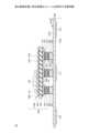
〈第1実施形態〉
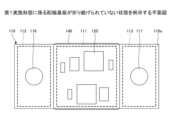
図1は、第1実施形態に係る回路モジュールを例示する平面図である。図2は、図1のA-A線に沿う断面図である。図1及び図2に示すように、回路モジュール1は、回路基板10と、電極付き基板20とを有している。 First Embodiment
Fig. 1 is a plan view illustrating a circuit module according to a first embodiment. Fig. 2 is a cross-sectional view taken along line A-A in Fig. 1. As shown in Figs. 1 and 2, the
(回路基板10)
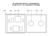
図3は、第1実施形態に係る配線基板が折り曲げられていない状態を例示する平面図である。図1~図3を参照すると、回路基板10は、配線基板110と、電子部品120と、接着層131~133と、磁気遮蔽部材140と、磁石151及び152とを有している。ただし、回路基板10は、磁石151及び152を有さず、必要なときに磁石151及び152を搭載できる構造としてもよい。 (Circuit board 10)
Fig. 3 is a plan view illustrating the wiring board according to the first embodiment in an unfolded state. With reference to Figs. 1 to 3, the
配線基板110は、可撓性を有する基板である。配線基板110は、例えば、ヤング率が低く可撓性を有する絶縁性樹脂上に、配線パターン、部品搭載用のパッド、絶縁層等を有している。ヤング率が低く可撓性を有する絶縁性樹脂としては、例えば、ポリイミド系樹脂やエポキシ系樹脂、ウレタン系樹脂、液晶ポリマー等が挙げられる。配線基板110の平面形状は、例えば、長方形であるが、これには限定されない。配線基板110の厚さは、例えば、20~100μm程度とすることができる。The
図3を参照すると、配線基板110の一方の面110aは、回路領域111と、端子領域112及び113とを含む。配線基板110が折り曲げられる前の状態で、回路領域111は、一方の面110aの長手方向の略中央に設けられている。また、端子領域112及び113は、一方の面110aの回路領域111の両外側に設けられている。Referring to FIG. 3, one
回路領域111には、複数の電子部品120が搭載されている。電子部品120は、半導体部品及び受動部品を含んでもよい。電子部品120は、例えば、生体信号を処理する回路を構成している。電子部品120を構成する半導体部品としては、例えば、信号処理用の集積回路等が挙げられる。電子部品120を構成する受動部品としては、例えば、抵抗、コンデンサ、インダクタ、アンテナ、コネクタ等が挙げられる。なお、配線基板110の他方の面110bには、電子部品等は実装されていない。The
端子領域112には接続端子116が配置され、端子領域113には接続端子117が配置されている。接続端子116及び117の平面形状は例えば円形であるが、矩形等であってもよい。接続端子116及び117は、図示しない配線により、電子部品120の必要な部分と電気的に接続されている。接続端子116及び117の材料としては、例えば、銅等を用いることができる。接続端子116及び117の厚さは、例えば、5~35μm程度とすることができる。A
図2を参照すると、複数の電子部品120が実装された配線基板110の他方の面110bは、接着層131~133を介して、磁気遮蔽部材140に固定されている。磁気遮蔽部材140は、第1主面140a、及び第1主面140aの反対面である第2主面140bを備えており、平面視で回路領域111より大きいことが好ましい。磁気遮蔽部材140としては、例えば、パーマロイやケイ素鋼等が挙げられる。磁気遮蔽部材140の厚さは、例えば、0.1~2mm程度とすることができる。磁気遮蔽部材140は、可撓性を有してもよい。また、接着層131~133としては、例えば、アクリル系樹脂やエポキシ系樹脂等が挙げられる。接着層131~133の供給形態としては、例えば、液状態やフィルム状態等が挙げられる。接着層131~133のそれぞれの厚さは、例えば、20~100μm程度とすることができる。Referring to FIG. 2, the
具体的には、配線基板110の他方の面110bにおいて、平面視で回路領域111と重複する領域は、接着層131を介して、磁気遮蔽部材140の第1主面140aに固定されている。すなわち、配線基板110の回路領域111は、磁気遮蔽部材140の第1主面140a上に配置されている。Specifically, on the
また、配線基板110の両端側は、回路領域111と端子領域112との間の領域、及び回路領域111と端子領域113との間の領域で磁気遮蔽部材140の両端部に沿って折り曲げられている。そして、配線基板110の他方の面110bにおいて、平面視で端子領域112と重複する領域は、接着層132を介して、磁気遮蔽部材140の第2主面140bに固定されている。In addition, both ends of the
また、配線基板110の他方の面110bにおいて、平面視で端子領域113と重複する領域は、接着層133を介して、磁気遮蔽部材140の第2主面140bに固定されている。すなわち、配線基板110の端子領域112及び113は、磁気遮蔽部材140の第2主面140b上に配置されている。このように、回路領域111と端子領域112及び113とは、断面視において、磁気遮蔽部材140を挟んで反対側に配置されている。In addition, on the
接続端子116には、例えば、はんだ等により、磁石151が接合されていてもよい。また、接続端子117には、例えば、はんだ等により、磁石152が接合されていてもよい。接続端子116及び117と磁石151及び152との接続信頼性を向上するため、及び電気抵抗を低くするため、磁石151及び152の表面には金属層155が形成されていることが好ましい。磁石151及び152の材料としては、例えば、フェライト、コバルト、ネオジウム等が挙げられる。金属層155の材料としては、例えば、銅や金等が挙げられる。金属層155は、例えば、無電解めっき法で形成できる。A
少なくとも磁石151、152が接合された接続端子116、117と平面視で対応する部分に相当する配線基板110の他方の面110bと磁気遮蔽部材140とが接着層を用いて強固に接合されている。The
(電極付き基板20)
電極付き基板20は、一方の面210aに強磁性体金属部251及び252を備え、他方の面210bに強磁性体金属部251及び252と電気的に接続された外部電極216及び217を備えた配線基板210を有している。配線基板210は、可撓性又は伸縮性を有する基板である。配線基板210は、例えば、絶縁性樹脂上に、配線パターン、部品搭載用のパッド、絶縁層等を有している。絶縁性樹脂としては、例えば、配線基板110と同様に、ポリイミド系樹脂やエポキシ系樹脂、液晶ポリマー等を用いることができる。配線基板210として、ウレタン等からなる伸縮性に優れた材料を用いてもよい。配線基板210の厚さは、例えば20~100μm程度とすることができる。 (Substrate with electrode 20)
The electrode-attached
配線基板210の一方の面210aにおいて、平面視で接続端子116及び117と重複する領域には図示しないパッドが形成され、図示しないパッド上には、例えば、はんだ等により、強磁性体金属部251及び252が接合されている。強磁性体金属部251及び252は突起電極であり、磁石151及び152と磁力により着脱自在に接続され、両者は電気的に接続されている。強磁性体金属部251及び252の材料としては、例えば、SUS430等が挙げられる。パッドとの接続信頼性を向上するため、及び電気抵抗を低くするため、強磁性体金属部251及び252の表面には金属層255が形成されていることが好ましい。金属層255の材料としては、例えば、銅や金等が挙げられる。金属層255は、例えば、無電解めっき法で形成できる。On one
なお、突起電極として、強磁性体金属部251及び252の代わりに磁石を用いてもよい。ただし、磁石は極性を持つため、磁石151及び152と吸着可能な極性に揃える必要がある。そのため、無極強の強磁性体金属部251及び252を突起電極として用いる方が、電極付き基板20の製造が容易である。In addition, magnets may be used as protruding electrodes instead of the
配線基板210の他方の面210bには、外部電極216及び217が設けられている。外部電極216及び217は、図示しない配線やスールーホール等を介して、強磁性体金属部251又は252が固定された各パッドと電気的に接続されている。外部電極216及び217は、測定対象と接して信号が入力される部分である。外部電極216及び217の材料としては、例えば、銅や銀等を用いることができる。外部電極216及び217のそれぞれの厚さは、例えば、5~35μm程度とすることができる。
外部電極216から入力した信号は、強磁性体金属部251、磁石151、接続端子116を経由して、電子部品120の必要な部分に入力される。また、外部電極217から入力した信号は、強磁性体金属部252、磁石152、接続端子117を経由して、電子部品120の必要な部分に入力される。The signal input from the
このように、回路基板10は、磁気遮蔽部材140の第1主面140a側に電子部品120が実装され、磁気遮蔽部材140の第2主面140b側に磁石151及び152と接続可能な接続端子116及び117が配置されている。これにより、接続端子116及び117に磁石151及び152等の磁界を発生する部品が配置された場合でも、磁石151及び152等の磁気が磁気遮蔽部材140により遮断される。そのため、磁石151及び152等の磁気に起因するノイズが電子部品120に与える影響を低減して、所望の出力信号を得ることが可能となる。In this way, the
また、一般に、磁気遮蔽部材140の材料として用いられるパーマロイやケイ素鋼等は、樹脂材料等に比べて加工が難しいため、貫通孔やビア等の層間接続構造を形成するとコスト上昇に繋がる。回路基板10では、電子部品120は配線基板110の一方の面110aのみに実装され、接続端子116及び117も配線基板110の一方の面110aのみに配置されている。そのため、回路基板10では、配線基板110を折り曲げるだけで電子部品120と接続端子116及び117とを磁気遮蔽部材140の反対面側に容易に配置可能であり、磁気遮蔽部材140に層間接続構造を形成する必要がなく、コストを抑えることができる。また、電子部品120や接続端子116等を磁気遮蔽部材140の両側に配置できるため、レイアウトの自由度を向上できる。In addition, generally, permalloy, silicon steel, etc., which are used as materials for the
また、回路基板10は、磁石151及び152の磁力で強磁性体金属部251及び252と着脱自在に接続されているため、必要なときのみに、電極付き基板20に取り付けることができる。In addition, the
回路モジュール1は、例えば、外部電極216及び217が生体と接することで、生体から各種の生体情報を検出するセンサとして利用できる。具体的には、回路モジュール1は、例えば、筋電センサとして利用できる。或いは、回路モジュール1は、心電センサや脳磁センサとして利用してもよい。The
〈第1実施形態の変形例1〉
第1実施形態の変形例1では、第1実施形態とは異なる配線基板を有する回路モジュールの例を示す。なお、第1実施形態の変形例1において、既に説明した実施形態と同一構成部品についての説明は省略する場合がある。 First Modification of the First Embodiment
In the first modification of the first embodiment, an example of a circuit module having a wiring board different from that of the first embodiment is shown. Note that in the first modification of the first embodiment, the description of the same components as those in the already described embodiments may be omitted.
図4は、第1実施形態の変形例1に係る回路モジュールを例示する断面図であり、図2に対応する断面を示している。図5は、第1実施形態の変形例1に係る配線基板が折り曲げられていない状態を例示する平面図である。図4及び図5を参照すると、回路モジュール1Aは、回路基板10が回路基板10Aに置換された点が、回路モジュール1(図1~図3参照)と相違する。Figure 4 is a cross-sectional view illustrating a circuit module according to
回路基板10Aは、配線基板110Aと、電子部品120と、接着層131及び132と、磁気遮蔽部材140と、磁石151及び152とを有している。ただし、回路基板10Aは、磁石151及び152を有さず、必要なときに磁石151及び152を搭載できる構造としてもよい。The
図5を参照すると、配線基板110Aの一方の面110aは、回路領域111Aと、端子領域112Aとを含む。配線基板110Aが折り曲げられる前の状態で、回路領域111Aは、一方の面110aの長手方向の一端側に設けられている。回路領域111Aには、複数の電子部品120が実装されている。なお、配線基板110Aの他方の面110bには、電子部品等は実装されていない。また、端子領域112Aは、一方の面110aの長手方向の他端側に回路領域111Aに隣接して設けられている。端子領域112Aには接続端子116及び117が配置されている。Referring to FIG. 5, one
図4を参照すると、複数の電子部品120が実装された配線基板110Aは、接着層131及び132を介して、磁気遮蔽部材140に固定されている。具体的には、配線基板110Aの他方の面110bにおいて、平面視で回路領域111Aと重複する領域は、接着層131を介して、磁気遮蔽部材140の第1主面140aに固定されている。すなわち、配線基板110Aの回路領域111Aは、磁気遮蔽部材140の第1主面140a上に配置されている。Referring to FIG. 4, the
また、配線基板110Aの他端側は、回路領域111Aと端子領域112Aとの間の領域で磁気遮蔽部材140の端部に沿って折り曲げられている。そして、配線基板110Aの他方の面110bにおいて、平面視で端子領域112Aと重複する領域は、接着層132を介して、磁気遮蔽部材140の第2主面140bに固定されている。すなわち、配線基板110Aの端子領域112Aは、磁気遮蔽部材140の第2主面140b上に配置されている。このように、回路領域111Aと端子領域112Aとは、断面視において、磁気遮蔽部材140を挟んで反対側に配置されている。The other end of the
このように、配線基板110Aが折り曲げられる前の状態で、接続端子116及び117が配置された1つの端子領域112Aが、一方の面110aの回路領域111Aの片側に設けられてもよい。この場合は、配線基板110Aは、回路領域111Aと端子領域112Aとの間の領域で磁気遮蔽部材140に沿って折り曲げられる。これにより、回路領域111Aは磁気遮蔽部材140の第1主面140a上に配置され、端子領域112Aは磁気遮蔽部材140の第2主面140b上に配置される。その結果、第1実施形態と同様の効果を奏する。In this way, before the
〈第2実施形態〉
第2実施形態では、外部電極を3つ以上有する回路モジュールの例を示す。なお、第2実施形態において、既に説明した実施形態と同一構成部品についての説明は省略する場合がある。 Second Embodiment
In the second embodiment, an example of a circuit module having three or more external electrodes will be described. Note that in the second embodiment, the description of the same components as those in the embodiments already described may be omitted.
図6は、第2実施形態に係る回路モジュールを例示する断面図であり、図2に対応する断面を示している。図7は、第2実施形態に係る配線基板が折り曲げられていない状態を例示する平面図である。図6及び図7を参照すると、回路モジュール1Bは、回路基板10が回路基板10Bに置換され、電極付き基板20が電極付き基板20Bに置換された点が、回路モジュール1(図1~図3参照)と相違する。Figure 6 is a cross-sectional view illustrating a circuit module according to the second embodiment, showing a cross section corresponding to Figure 2. Figure 7 is a plan view illustrating a wiring board according to the second embodiment in an unbent state. With reference to Figures 6 and 7,
回路基板10Bは、配線基板110Bと、電子部品120と、接着層131及び132と、磁気遮蔽部材140と、磁石151~153とを有している。ただし、回路基板10Bは、磁石151~153を有さず、必要なときに磁石151~153を搭載できる構造としてもよい。The
図7を参照すると、配線基板110Bの一方の面110aは、回路領域111Bと、端子領域112Bとを含む。配線基板110Bが折り曲げられる前の状態で、回路領域111Bは、一方の面110aの長手方向の一端側に設けられている。回路領域111Bには、複数の電子部品120が実装されている。なお、配線基板110Bの他方の面110bには、電子部品等は実装されておらず、配線や電極も形成されていない。また、端子領域112Bは、一方の面110aの長手方向の他端側に回路領域111Bに隣接して設けられている。端子領域112Bには接続端子116、117、及び118が配置されている。Referring to FIG. 7, one
図6を参照すると、配線基板110Bの回路領域111Bは磁気遮蔽部材140の第1主面140a上に配置され、端子領域112Bは磁気遮蔽部材140の第2主面140b上に配置されている。このように、回路領域111Bと端子領域112Bとは、断面視において、磁気遮蔽部材140を挟んで反対側に配置されている。Referring to FIG. 6, the
接続端子118には、例えば、はんだ等により、磁石153が固定されていてもよい。接続端子118と磁石153との接続信頼性を向上するため、及び電気抵抗を低くするため、磁石153の表面には金属層155が形成されていることが好ましい。磁石153の材料としては、例えば、磁石151及び152と同様の材料を用いることができる。The
電極付き基板20Bは、配線基板210Bと、強磁性体金属部251~253とを有している。配線基板210Bの一方の面210aにおいて、平面視で接続端子118と重複する領域には図示しないパッドが形成され、図示しないパッド上には、例えば、はんだ等により、強磁性体金属部253が接合されている。強磁性体金属部253は突起電極であり、磁石153と磁力により着脱自在に接続され、両者は電気的に接続されている。強磁性体金属部253の材料としては、例えば、強磁性体金属部251及び252と同様の材料を用いることができる。強磁性体金属部253の表面には金属層255が形成されていることが好ましい。The electrode-equipped
なお、突起電極として、強磁性体金属部253の代わりに磁石を用いてもよい。ただし、磁石は極性を持つため、磁石153と吸着可能な極性に揃える必要がある。そのため、無極の強磁性体金属部253を突起電極として用いる方が、電極付き基板20Bの製造が容易である。In addition, a magnet may be used as the protruding electrode instead of the
配線基板210Bの他方の面210bには、外部電極216~218が例えば配線基板210の長手方向に沿って設けられている。外部電極218は、図示しない配線やスールーホール等を介して、強磁性体金属部253が固定されたパッドと電気的に接続されている。外部電極216~218は、測定対象と接して信号が入力される部分である。外部電極218の材料としては、例えば、外部電極216及び217と同様の材料を用いることができる。外部電極218から入力した信号は、強磁性体金属部253、磁石153、接続端子118を経由して、電子部品120の必要な部分に入力される。外部電極216~218のうちの1つは、参照電極として使用することができる。On the
このように、配線基板110Bが折り曲げられる前の状態で、接続端子116~118が配置された1つの端子領域112Bが、一方の面110aの回路領域111Bの片側に設けられてもよい。この場合も、配線基板110Aの場合と同様に、配線基板110Bは、回路領域111Bと端子領域112Bとの間の領域で磁気遮蔽部材140に沿って折り曲げられる。これにより、回路領域111Bは磁気遮蔽部材140の第1主面140a上に配置され、端子領域112Bは磁気遮蔽部材140の第2主面140b上に配置される。その結果、第1実施形態と同様の効果を奏する。In this way, before the
また、例えば、回路モジュール1Bを筋電センサとして使用する場合、参照電極は、筋電信号の基準電位となる。そのため、回路モジュール1Bにおいて、接続端子116~118と電気的に接続された外部電極216~218のうちの1つを参照電極として使用することで、より安定的な筋電信号の検出が可能となる。For example, when the
〈第2実施形態の変形例1〉
第2実施形態の変形例1では、外部電極を3つ以上有する回路モジュールの他の例を示す。なお、第2実施形態の変形例1において、既に説明した実施形態と同一構成部品についての説明は省略する場合がある。 <
In the first modification of the second embodiment, another example of a circuit module having three or more external electrodes is shown. Note that in the first modification of the second embodiment, the description of the same components as those in the already described embodiments may be omitted.
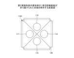
図8は、第2実施形態の変形例1に係る配線基板が折り曲げられていない状態を例示する平面図である。図9は、第2実施形態の変形例1に係る配線基板が折り曲げられた状態を例示する底面図である。Figure 8 is a plan view illustrating a state in which the wiring board according to the first modified example of the second embodiment is not bent. Figure 9 is a bottom view illustrating a state in which the wiring board according to the first modified example of the second embodiment is bent.
図8及び図9を参照すると、配線基板110Cが折り曲げられる前の状態で、回路領域111Cは、平面視で4つの辺を備えている。そして、端子領域112C、113C、及び114Cが、配線基板110Cの一方の面110aの回路領域111Cの3辺の外側に延伸している。端子領域112C、113C、及び114Cには、それぞれ接続端子116、117、及び118が設けられている。Referring to Figures 8 and 9, before the
配線基板110Cは、回路領域111Cと端子領域112C、113C、及び114Cとの間の領域で磁気遮蔽部材140に沿って折り曲げられる。これにより、回路領域111Cは磁気遮蔽部材140の第1主面140a上に配置され、端子領域112C、113C、及び114Cは磁気遮蔽部材140の第2主面140b上に配置される。その結果、第1実施形態と同様の効果を奏する。端子領域112C、113C、及び114Cは、折り曲げられたときに磁気遮蔽部材140の第2主面140b上で重ならないような適宜な形状とすることができる。The
また、例えば、第2実施形態の変形例1に係る回路モジュールを筋電センサとして使用する場合、参照電極は、筋電信号の基準電位となる。そのため、第2実施形態の変形例1に係る回路モジュールにおいて、接続端子116~118と電気的に接続された外部電極のうちの1つを参照電極として使用することで、より安定的な筋電信号の検出が可能となる。For example, when the circuit module according to the first modified example of the second embodiment is used as an electromyogram sensor, the reference electrode serves as the reference potential of the electromyogram signal. Therefore, in the circuit module according to the first modified example of the second embodiment, by using one of the external electrodes electrically connected to the
〈第2実施形態の変形例2〉
第2実施形態の変形例2では、外部電極を3つ以上有する回路モジュールの他の例を示す。なお、第2実施形態の変形例2において、既に説明した実施形態と同一構成部品についての説明は省略する場合がある。 <Modification 2 of the Second Embodiment>
In the second modification of the second embodiment, another example of a circuit module having three or more external electrodes is shown. Note that in the second modification of the second embodiment, the description of the same components as those in the already described embodiment may be omitted.
図10は、第2実施形態の変形例2に係る配線基板が折り曲げられていない状態を例示する平面図である。図11は、第2実施形態の変形例2に係る配線基板が折り曲げられた状態を例示する底面図である。Figure 10 is a plan view illustrating a state in which the wiring board according to the second modification of the second embodiment is not bent. Figure 11 is a bottom view illustrating a state in which the wiring board according to the second modification of the second embodiment is bent.
図10及び図11を参照すると、配線基板110Dが折り曲げられる前の状態で、回路領域111Dは、平面視で4つの辺を備えている。そして、端子領域112D、113D、114D、及び115Dが、配線基板110Dの一方の面110aの回路領域111Dの4辺の外側に延伸している。端子領域112D、113D、114D、及び115Dには、それぞれ接続端子116、117、118、及び119が設けられている。Referring to Figures 10 and 11, before the
配線基板110Dは、回路領域111Dと端子領域112D、113D、及び114Dとの間の領域で磁気遮蔽部材140に沿って折り曲げられる。これにより、回路領域111Dは磁気遮蔽部材140の第1主面140a上に配置され、端子領域112D、113D、114D、及び115Dは磁気遮蔽部材140の第2主面140b上に配置される。その結果、第1実施形態と同様の効果を奏する。端子領域112D、113D、114D、及び115Dは、折り曲げられたときに磁気遮蔽部材140の第2主面140b上で重ならないような適宜な形状とすることができる。The
また、例えば、第2実施形態の変形例2に係る回路モジュールを筋電センサとして使用する場合、参照電極は、筋電信号の基準電位となる。そのため、第2実施形態の変形例2に係る回路モジュールにおいて、接続端子116~119と電気的に接続された外部電極のうちの2つを参照電極として使用することで、より安定的な筋電信号の検出が可能となる。For example, when the circuit module according to the second modification of the second embodiment is used as an electromyogram sensor, the reference electrode serves as the reference potential of the electromyogram signal. Therefore, in the circuit module according to the second modification of the second embodiment, by using two of the external electrodes electrically connected to the
以上、好ましい実施形態等について詳説したが、上述した実施形態等に制限されることはなく、特許請求の範囲に記載された範囲を逸脱することなく、上述した実施形態等に種々の変形及び置換を加えることができる。Although the preferred embodiments have been described above in detail, the present invention is not limited to the above-described embodiments, and various modifications and substitutions can be made to the above-described embodiments without departing from the scope of the claims.
1、1A、1B 回路モジュール
10、10A、10B 回路基板
20、20B 電極付き基板
110、110A、110B、110C、110D、210、210B 配線基板
110a、210a 一方の面
110b、210b 他方の面
111、111A、111B、111C、111D 回路領域
112、112A、112B、112C、112D、113、113C、113D、114、114C、114D、115、115D 端子領域
116、117、118、119 接続端子
120 電子部品
131、132、133 接着層
140 磁気遮蔽部材
140a 第1主面
140b 第2主面
151、152、153 磁石
155、255 金属層
216、217、218 外部電極
251、252 強磁性体金属部1, 1A,
Claims (10)
Translated fromJapanese一方の面、及び前記一方の面の反対面である他方の面を備え、前記他方の面が前記磁気遮蔽部材の前記第1主面及び前記第2主面に固定された可撓性の配線基板と、を有し、
前記配線基板の一方の面は、電子部品が搭載された回路領域と、接続端子が配置された端子領域と、を含み、
前記回路領域は、前記磁気遮蔽部材の前記第1主面上に配置され、
前記配線基板が前記磁気遮蔽部材に沿って折り曲げられ、前記端子領域は、前記磁気遮蔽部材の第2主面上に配置される、回路基板。 a magnetic shielding member having a first main surface and a second main surface opposite to the first main surface;
a flexible wiring board having one surface and another surface opposite to the one surface, the other surface being fixed to the first main surface and the second main surface of the magnetic shielding member,
one surface of the wiring board includes a circuit region on which electronic components are mounted and a terminal region on which connection terminals are arranged;
the circuit region is disposed on the first main surface of the magnetic shielding member,
the wiring board is folded along the magnetic shielding member, and the terminal area is disposed on a second main surface of the magnetic shielding member.
前記配線基板が前記回路領域と前記端子領域との間の領域で前記磁気遮蔽部材に沿って折り曲げられ、前記端子領域は、前記磁気遮蔽部材の第2主面上に配置される、請求項1乃至3の何れか一項に記載の回路基板。 one of the terminal areas in which the plurality of connection terminals are arranged is provided on one side of the circuit area on the one surface before the wiring board is folded;
4. The circuit board according to claim 1, wherein the wiring board is folded along the magnetic shielding member in a region between the circuit region and the terminal region, and the terminal region is disposed on a second main surface of the magnetic shielding member.
前記配線基板が前記回路領域と各々の前記端子領域との間の領域で前記磁気遮蔽部材に沿って折り曲げられ、各々の前記端子領域は、前記磁気遮蔽部材の第2主面上に配置される、請求項1乃至3の何れか一項に記載の回路基板。 the terminal areas are provided outside the circuit area on the one surface before the wiring board is folded;
4. The circuit board according to claim 1, wherein the wiring board is folded along the magnetic shielding member in a region between the circuit region and each of the terminal regions, and each of the terminal regions is disposed on a second main surface of the magnetic shielding member.
前記配線基板が折り曲げられる前の状態で、3つの前記端子領域が、前記一方の面の前記回路領域の3辺の外側に延伸する、請求項5に記載の回路基板。 the circuit region has four sides in a plan view,
The circuit board according to claim 5 , wherein the three terminal areas extend outside three sides of the circuit area on the one surface before the wiring board is folded.
前記配線基板が折り曲げられる前の状態で、4つの前記端子領域が、前記一方の面の前記回路領域の4辺の外側に延伸する、請求項5に記載の回路基板。 the circuit region has four sides in a plan view,
The circuit board according to claim 5 , wherein the four terminal areas extend outside four sides of the circuit area on the one surface before the wiring board is folded.
一方の面に突起電極を備え、他方の面に前記突起電極と電気的に接続された外部電極を備えた基板と、を有し、
前記磁石と前記突起電極とが着脱自在に接続された回路モジュール。 A circuit board according to claim 2;
a substrate having protruding electrodes on one surface and having external electrodes electrically connected to the protruding electrodes on the other surface;
The magnet and the protruding electrodes are detachably connected to a circuit module.
Priority Applications (2)
| Application Number | Priority Date | Filing Date | Title |
|---|---|---|---|
| JP2021123546AJP7597449B2 (en) | 2021-07-28 | 2021-07-28 | Circuit boards, circuit modules |
| US17/811,947US12108520B2 (en) | 2021-07-28 | 2022-07-12 | Circuit board and circuit module |
Applications Claiming Priority (1)
| Application Number | Priority Date | Filing Date | Title |
|---|---|---|---|
| JP2021123546AJP7597449B2 (en) | 2021-07-28 | 2021-07-28 | Circuit boards, circuit modules |
Publications (2)
| Publication Number | Publication Date |
|---|---|
| JP2023019075A JP2023019075A (en) | 2023-02-09 |
| JP7597449B2true JP7597449B2 (en) | 2024-12-10 |
Family
ID=85039377
Family Applications (1)
| Application Number | Title | Priority Date | Filing Date |
|---|---|---|---|
| JP2021123546AActiveJP7597449B2 (en) | 2021-07-28 | 2021-07-28 | Circuit boards, circuit modules |
Country Status (2)
| Country | Link |
|---|---|
| US (1) | US12108520B2 (en) |
| JP (1) | JP7597449B2 (en) |
Families Citing this family (2)
| Publication number | Priority date | Publication date | Assignee | Title |
|---|---|---|---|---|
| KR102790199B1 (en)* | 2021-01-05 | 2025-04-03 | 주식회사 엘지에너지솔루션 | Connection structure |
| JP7638099B2 (en)* | 2021-01-27 | 2025-03-03 | メクテック株式会社 | Voltage Monitoring Module |
Citations (3)
| Publication number | Priority date | Publication date | Assignee | Title |
|---|---|---|---|---|
| JP2006156597A (en) | 2004-11-26 | 2006-06-15 | Kyocera Corp | Wiring board |
| JP6342596B1 (en) | 2018-01-31 | 2018-06-13 | 東和株式会社 | clothing |
| WO2019009062A1 (en) | 2017-07-07 | 2019-01-10 | 株式会社村田製作所 | High frequency power circuit module |
Family Cites Families (6)
| Publication number | Priority date | Publication date | Assignee | Title |
|---|---|---|---|---|
| JPH06295935A (en)* | 1993-04-07 | 1994-10-21 | Hitachi Ltd | Semiconductor package |
| JP2810647B2 (en)* | 1996-04-30 | 1998-10-15 | 山一電機株式会社 | IC package |
| JP2006332648A (en)* | 2005-05-20 | 2006-12-07 | Sumitomo Electric Ind Ltd | Connection structure of multi-pin coaxial module and circuit board using flexible board |
| JP2016090295A (en) | 2014-10-31 | 2016-05-23 | 日本精機株式会社 | Instrument device |
| US10892085B2 (en)* | 2016-12-09 | 2021-01-12 | Astec International Limited | Circuit board assemblies having magnetic components |
| US12101873B2 (en)* | 2022-04-25 | 2024-09-24 | Microsoft Technology Licensing, Llc | Flexible printed circuit cable assembly with electromagnetic shielding |
- 2021
- 2021-07-28JPJP2021123546Apatent/JP7597449B2/enactiveActive
- 2022
- 2022-07-12USUS17/811,947patent/US12108520B2/enactiveActive
Patent Citations (3)
| Publication number | Priority date | Publication date | Assignee | Title |
|---|---|---|---|---|
| JP2006156597A (en) | 2004-11-26 | 2006-06-15 | Kyocera Corp | Wiring board |
| WO2019009062A1 (en) | 2017-07-07 | 2019-01-10 | 株式会社村田製作所 | High frequency power circuit module |
| JP6342596B1 (en) | 2018-01-31 | 2018-06-13 | 東和株式会社 | clothing |
Also Published As
| Publication number | Publication date |
|---|---|
| US20230031168A1 (en) | 2023-02-02 |
| JP2023019075A (en) | 2023-02-09 |
| US12108520B2 (en) | 2024-10-01 |
Similar Documents
| Publication | Publication Date | Title |
|---|---|---|
| JP3647307B2 (en) | Printed circuit board and electronic device | |
| US9252489B2 (en) | Circuit board and circuit module | |
| JP7597449B2 (en) | Circuit boards, circuit modules | |
| KR20060061825A (en) | Current sensor | |
| US20080003846A1 (en) | Circuit board unit | |
| US20220320259A1 (en) | Flexible substrate and electronic device | |
| CN112970336A (en) | Electronic device and connecting member | |
| TWI755555B (en) | Printed circuit board and electronic device having the same | |
| TW447053B (en) | Semiconductor apparatus and its manufacturing method, circuit board and electronic machine | |
| US12336085B2 (en) | Structure and structure with electronic component | |
| JPH04196555A (en) | Tab package | |
| JP6460280B2 (en) | Component mounting board | |
| TWI898398B (en) | Transducer wire board and method for manufacturing the same | |
| WO2020009029A1 (en) | Flexible substrate, method for manufacturing same, and electronic device | |
| JP2023019076A (en) | circuit board | |
| US20050206011A1 (en) | Circuit module | |
| JP5845792B2 (en) | Electronic components | |
| JP2009063385A (en) | Magnetometric sensor package | |
| WO2023190611A1 (en) | High-frequency module | |
| TW202505294A (en) | Wiring circuit board | |
| JPH11326372A (en) | Contact probe and probe device | |
| CN105682354A (en) | Flexible-rigid combined board and terminal | |
| US9288916B2 (en) | Electronic device, cable coupling structure, and method of fabricating electronic device | |
| US20050012213A1 (en) | Wiring board, stacked wiring board and method of manufacturing the same, semiconductor device and method of manufacturing the same, circuit board, and electronic instrument | |
| JPH0534132Y2 (en) |
Legal Events
| Date | Code | Title | Description |
|---|---|---|---|
| A621 | Written request for application examination | Free format text:JAPANESE INTERMEDIATE CODE: A621 Effective date:20240402 | |
| TRDD | Decision of grant or rejection written | ||
| A977 | Report on retrieval | Free format text:JAPANESE INTERMEDIATE CODE: A971007 Effective date:20241024 | |
| A01 | Written decision to grant a patent or to grant a registration (utility model) | Free format text:JAPANESE INTERMEDIATE CODE: A01 Effective date:20241029 | |
| A61 | First payment of annual fees (during grant procedure) | Free format text:JAPANESE INTERMEDIATE CODE: A61 Effective date:20241125 | |
| R150 | Certificate of patent or registration of utility model | Ref document number:7597449 Country of ref document:JP Free format text:JAPANESE INTERMEDIATE CODE: R150 |