JP7596842B2 - Method for manufacturing a wiring board - Google Patents
Method for manufacturing a wiring boardDownload PDFInfo
- Publication number
- JP7596842B2 JP7596842B2JP2021025668AJP2021025668AJP7596842B2JP 7596842 B2JP7596842 B2JP 7596842B2JP 2021025668 AJP2021025668 AJP 2021025668AJP 2021025668 AJP2021025668 AJP 2021025668AJP 7596842 B2JP7596842 B2JP 7596842B2
- Authority
- JP
- Japan
- Prior art keywords
- layer
- insulating layer
- seed layer
- insulating
- resin
- Prior art date
- Legal status (The legal status is an assumption and is not a legal conclusion. Google has not performed a legal analysis and makes no representation as to the accuracy of the status listed.)
- Active
Links
Images


Classifications
- H—ELECTRICITY
- H05—ELECTRIC TECHNIQUES NOT OTHERWISE PROVIDED FOR
- H05K—PRINTED CIRCUITS; CASINGS OR CONSTRUCTIONAL DETAILS OF ELECTRIC APPARATUS; MANUFACTURE OF ASSEMBLAGES OF ELECTRICAL COMPONENTS
- H05K3/00—Apparatus or processes for manufacturing printed circuits
- H05K3/10—Apparatus or processes for manufacturing printed circuits in which conductive material is applied to the insulating support in such a manner as to form the desired conductive pattern
- H05K3/108—Apparatus or processes for manufacturing printed circuits in which conductive material is applied to the insulating support in such a manner as to form the desired conductive pattern by semi-additive methods; masks therefor
- H—ELECTRICITY
- H05—ELECTRIC TECHNIQUES NOT OTHERWISE PROVIDED FOR
- H05K—PRINTED CIRCUITS; CASINGS OR CONSTRUCTIONAL DETAILS OF ELECTRIC APPARATUS; MANUFACTURE OF ASSEMBLAGES OF ELECTRICAL COMPONENTS
- H05K3/00—Apparatus or processes for manufacturing printed circuits
- H05K3/10—Apparatus or processes for manufacturing printed circuits in which conductive material is applied to the insulating support in such a manner as to form the desired conductive pattern
- H05K3/101—Apparatus or processes for manufacturing printed circuits in which conductive material is applied to the insulating support in such a manner as to form the desired conductive pattern by casting or moulding of conductive material
- C—CHEMISTRY; METALLURGY
- C25—ELECTROLYTIC OR ELECTROPHORETIC PROCESSES; APPARATUS THEREFOR
- C25D—PROCESSES FOR THE ELECTROLYTIC OR ELECTROPHORETIC PRODUCTION OF COATINGS; ELECTROFORMING; APPARATUS THEREFOR
- C25D17/00—Constructional parts, or assemblies thereof, of cells for electrolytic coating
- C25D17/10—Electrodes, e.g. composition, counter electrode
- C25D17/14—Electrodes, e.g. composition, counter electrode for pad-plating
- C—CHEMISTRY; METALLURGY
- C25—ELECTROLYTIC OR ELECTROPHORETIC PROCESSES; APPARATUS THEREFOR
- C25D—PROCESSES FOR THE ELECTROLYTIC OR ELECTROPHORETIC PRODUCTION OF COATINGS; ELECTROFORMING; APPARATUS THEREFOR
- C25D5/00—Electroplating characterised by the process; Pretreatment or after-treatment of workpieces
- C25D5/02—Electroplating of selected surface areas
- C25D5/022—Electroplating of selected surface areas using masking means
- C—CHEMISTRY; METALLURGY
- C25—ELECTROLYTIC OR ELECTROPHORETIC PROCESSES; APPARATUS THEREFOR
- C25D—PROCESSES FOR THE ELECTROLYTIC OR ELECTROPHORETIC PRODUCTION OF COATINGS; ELECTROFORMING; APPARATUS THEREFOR
- C25D5/00—Electroplating characterised by the process; Pretreatment or after-treatment of workpieces
- C25D5/04—Electroplating with moving electrodes
- C25D5/06—Brush or pad plating
- C—CHEMISTRY; METALLURGY
- C25—ELECTROLYTIC OR ELECTROPHORETIC PROCESSES; APPARATUS THEREFOR
- C25D—PROCESSES FOR THE ELECTROLYTIC OR ELECTROPHORETIC PRODUCTION OF COATINGS; ELECTROFORMING; APPARATUS THEREFOR
- C25D5/00—Electroplating characterised by the process; Pretreatment or after-treatment of workpieces
- C25D5/54—Electroplating of non-metallic surfaces
- C25D5/56—Electroplating of non-metallic surfaces of plastics
- C—CHEMISTRY; METALLURGY
- C25—ELECTROLYTIC OR ELECTROPHORETIC PROCESSES; APPARATUS THEREFOR
- C25D—PROCESSES FOR THE ELECTROLYTIC OR ELECTROPHORETIC PRODUCTION OF COATINGS; ELECTROFORMING; APPARATUS THEREFOR
- C25D7/00—Electroplating characterised by the article coated
- H—ELECTRICITY
- H05—ELECTRIC TECHNIQUES NOT OTHERWISE PROVIDED FOR
- H05K—PRINTED CIRCUITS; CASINGS OR CONSTRUCTIONAL DETAILS OF ELECTRIC APPARATUS; MANUFACTURE OF ASSEMBLAGES OF ELECTRICAL COMPONENTS
- H05K3/00—Apparatus or processes for manufacturing printed circuits
- H05K3/0011—Working of insulating substrates or insulating layers
- H05K3/0017—Etching of the substrate by chemical or physical means
- H05K3/0026—Etching of the substrate by chemical or physical means by laser ablation
- H—ELECTRICITY
- H05—ELECTRIC TECHNIQUES NOT OTHERWISE PROVIDED FOR
- H05K—PRINTED CIRCUITS; CASINGS OR CONSTRUCTIONAL DETAILS OF ELECTRIC APPARATUS; MANUFACTURE OF ASSEMBLAGES OF ELECTRICAL COMPONENTS
- H05K3/00—Apparatus or processes for manufacturing printed circuits
- H05K3/10—Apparatus or processes for manufacturing printed circuits in which conductive material is applied to the insulating support in such a manner as to form the desired conductive pattern
- H05K3/18—Apparatus or processes for manufacturing printed circuits in which conductive material is applied to the insulating support in such a manner as to form the desired conductive pattern using precipitation techniques to apply the conductive material
- H—ELECTRICITY
- H05—ELECTRIC TECHNIQUES NOT OTHERWISE PROVIDED FOR
- H05K—PRINTED CIRCUITS; CASINGS OR CONSTRUCTIONAL DETAILS OF ELECTRIC APPARATUS; MANUFACTURE OF ASSEMBLAGES OF ELECTRICAL COMPONENTS
- H05K3/00—Apparatus or processes for manufacturing printed circuits
- H05K3/10—Apparatus or processes for manufacturing printed circuits in which conductive material is applied to the insulating support in such a manner as to form the desired conductive pattern
- H05K3/20—Apparatus or processes for manufacturing printed circuits in which conductive material is applied to the insulating support in such a manner as to form the desired conductive pattern by affixing prefabricated conductor pattern
- H—ELECTRICITY
- H05—ELECTRIC TECHNIQUES NOT OTHERWISE PROVIDED FOR
- H05K—PRINTED CIRCUITS; CASINGS OR CONSTRUCTIONAL DETAILS OF ELECTRIC APPARATUS; MANUFACTURE OF ASSEMBLAGES OF ELECTRICAL COMPONENTS
- H05K3/00—Apparatus or processes for manufacturing printed circuits
- H05K3/38—Improvement of the adhesion between the insulating substrate and the metal
- H05K3/381—Improvement of the adhesion between the insulating substrate and the metal by special treatment of the substrate
- C—CHEMISTRY; METALLURGY
- C25—ELECTROLYTIC OR ELECTROPHORETIC PROCESSES; APPARATUS THEREFOR
- C25D—PROCESSES FOR THE ELECTROLYTIC OR ELECTROPHORETIC PRODUCTION OF COATINGS; ELECTROFORMING; APPARATUS THEREFOR
- C25D3/00—Electroplating: Baths therefor
- C25D3/02—Electroplating: Baths therefor from solutions
- C25D3/38—Electroplating: Baths therefor from solutions of copper
- H—ELECTRICITY
- H05—ELECTRIC TECHNIQUES NOT OTHERWISE PROVIDED FOR
- H05K—PRINTED CIRCUITS; CASINGS OR CONSTRUCTIONAL DETAILS OF ELECTRIC APPARATUS; MANUFACTURE OF ASSEMBLAGES OF ELECTRICAL COMPONENTS
- H05K2201/00—Indexing scheme relating to printed circuits covered by H05K1/00
- H05K2201/03—Conductive materials
- H05K2201/0332—Structure of the conductor
- H05K2201/0335—Layered conductors or foils
- H05K2201/0338—Layered conductor, e.g. layered metal substrate, layered finish layer or layered thin film adhesion layer
- H—ELECTRICITY
- H05—ELECTRIC TECHNIQUES NOT OTHERWISE PROVIDED FOR
- H05K—PRINTED CIRCUITS; CASINGS OR CONSTRUCTIONAL DETAILS OF ELECTRIC APPARATUS; MANUFACTURE OF ASSEMBLAGES OF ELECTRICAL COMPONENTS
- H05K2203/00—Indexing scheme relating to apparatus or processes for manufacturing printed circuits covered by H05K3/00
- H05K2203/05—Patterning and lithography; Masks; Details of resist
- H05K2203/0562—Details of resist
- H05K2203/0597—Resist applied over the edges or sides of conductors, e.g. for protection during etching or plating
- H—ELECTRICITY
- H05—ELECTRIC TECHNIQUES NOT OTHERWISE PROVIDED FOR
- H05K—PRINTED CIRCUITS; CASINGS OR CONSTRUCTIONAL DETAILS OF ELECTRIC APPARATUS; MANUFACTURE OF ASSEMBLAGES OF ELECTRICAL COMPONENTS
- H05K2203/00—Indexing scheme relating to apparatus or processes for manufacturing printed circuits covered by H05K3/00
- H05K2203/07—Treatments involving liquids, e.g. plating, rinsing
- H05K2203/0703—Plating
- H05K2203/0713—Plating poison, e.g. for selective plating or for preventing plating on resist
- H—ELECTRICITY
- H05—ELECTRIC TECHNIQUES NOT OTHERWISE PROVIDED FOR
- H05K—PRINTED CIRCUITS; CASINGS OR CONSTRUCTIONAL DETAILS OF ELECTRIC APPARATUS; MANUFACTURE OF ASSEMBLAGES OF ELECTRICAL COMPONENTS
- H05K2203/00—Indexing scheme relating to apparatus or processes for manufacturing printed circuits covered by H05K3/00
- H05K2203/07—Treatments involving liquids, e.g. plating, rinsing
- H05K2203/0703—Plating
- H05K2203/0723—Electroplating, e.g. finish plating
- H—ELECTRICITY
- H05—ELECTRIC TECHNIQUES NOT OTHERWISE PROVIDED FOR
- H05K—PRINTED CIRCUITS; CASINGS OR CONSTRUCTIONAL DETAILS OF ELECTRIC APPARATUS; MANUFACTURE OF ASSEMBLAGES OF ELECTRICAL COMPONENTS
- H05K2203/00—Indexing scheme relating to apparatus or processes for manufacturing printed circuits covered by H05K3/00
- H05K2203/10—Using electric, magnetic and electromagnetic fields; Using laser light
- H05K2203/107—Using laser light
- H—ELECTRICITY
- H05—ELECTRIC TECHNIQUES NOT OTHERWISE PROVIDED FOR
- H05K—PRINTED CIRCUITS; CASINGS OR CONSTRUCTIONAL DETAILS OF ELECTRIC APPARATUS; MANUFACTURE OF ASSEMBLAGES OF ELECTRICAL COMPONENTS
- H05K2203/00—Indexing scheme relating to apparatus or processes for manufacturing printed circuits covered by H05K3/00
- H05K2203/11—Treatments characterised by their effect, e.g. heating, cooling, roughening
- H05K2203/1173—Differences in wettability, e.g. hydrophilic or hydrophobic areas
- H—ELECTRICITY
- H05—ELECTRIC TECHNIQUES NOT OTHERWISE PROVIDED FOR
- H05K—PRINTED CIRCUITS; CASINGS OR CONSTRUCTIONAL DETAILS OF ELECTRIC APPARATUS; MANUFACTURE OF ASSEMBLAGES OF ELECTRICAL COMPONENTS
- H05K3/00—Apparatus or processes for manufacturing printed circuits
- H05K3/0011—Working of insulating substrates or insulating layers
- H05K3/0017—Etching of the substrate by chemical or physical means
- H05K3/0026—Etching of the substrate by chemical or physical means by laser ablation
- H05K3/0032—Etching of the substrate by chemical or physical means by laser ablation of organic insulating material
- Y—GENERAL TAGGING OF NEW TECHNOLOGICAL DEVELOPMENTS; GENERAL TAGGING OF CROSS-SECTIONAL TECHNOLOGIES SPANNING OVER SEVERAL SECTIONS OF THE IPC; TECHNICAL SUBJECTS COVERED BY FORMER USPC CROSS-REFERENCE ART COLLECTIONS [XRACs] AND DIGESTS
- Y02—TECHNOLOGIES OR APPLICATIONS FOR MITIGATION OR ADAPTATION AGAINST CLIMATE CHANGE
- Y02E—REDUCTION OF GREENHOUSE GAS [GHG] EMISSIONS, RELATED TO ENERGY GENERATION, TRANSMISSION OR DISTRIBUTION
- Y02E60/00—Enabling technologies; Technologies with a potential or indirect contribution to GHG emissions mitigation
- Y02E60/30—Hydrogen technology
- Y02E60/50—Fuel cells
Landscapes
- Engineering & Computer Science (AREA)
- Chemical & Material Sciences (AREA)
- Manufacturing & Machinery (AREA)
- Microelectronics & Electronic Packaging (AREA)
- Metallurgy (AREA)
- Organic Chemistry (AREA)
- Chemical Kinetics & Catalysis (AREA)
- Electrochemistry (AREA)
- Materials Engineering (AREA)
- Optics & Photonics (AREA)
- Physics & Mathematics (AREA)
- Manufacturing Of Printed Wiring (AREA)
- Manufacturing Of Printed Circuit Boards (AREA)
- Electroplating Methods And Accessories (AREA)
- Production Of Multi-Layered Print Wiring Board (AREA)
- Internal Circuitry In Semiconductor Integrated Circuit Devices (AREA)
Description
Translated fromJapanese本発明は、配線基板の製造方法に関する。The present invention relates to a method for manufacturing a wiring board.
配線基板の製造方法として、サブトラクティブ法、セミアディティブ法、及びフルアディティブ法が知られている。一般に、高密度な配線基板の製造には、セミアディティブ法が用いられる。The subtractive method, the semi-additive method, and the full-additive method are known as methods for manufacturing wiring boards. In general, the semi-additive method is used to manufacture high-density wiring boards.
特許文献1には、セミアディティブ法を用いた配線基板の製造方法が開示されている。具体的には、ベース層、誘電体層、シード層、及び第1めっき層をこの順に積層し、フォトリソグラフィー法により、第1めっき層上にパターン付きレジストを形成し、第1めっき層の、パターン付きレジストから露出した部分上に、第2めっき層を形成し、次いで、パターン付きレジストを除去し、第2めっき層をマスクとして第1めっき層及びシード層を除去して、配線基板を製造している。Patent Document 1 discloses a method for manufacturing a wiring board using a semi-additive method. Specifically, a base layer, a dielectric layer, a seed layer, and a first plating layer are laminated in this order, a patterned resist is formed on the first plating layer by photolithography, a second plating layer is formed on the portion of the first plating layer that is exposed from the patterned resist, the patterned resist is then removed, and the first plating layer and the seed layer are removed using the second plating layer as a mask to manufacture the wiring board.
特許文献1に記載されるようなめっき法を用いたセミアディティブ法では、形成する第2めっき層の厚み以上の厚みを有するパターン付きレジストを形成する必要がある。しかし、厚みの大きいパターン付きレジストの形成は、多くの工程を要する。また、このようなパターン付きレジストの除去は、多くの工程を要するだけでなく、多量の廃液を発生させる。In the semi-additive method using plating as described in Patent Document 1, it is necessary to form a patterned resist having a thickness equal to or greater than the thickness of the second plating layer to be formed. However, forming a thick patterned resist requires many steps. Furthermore, removing such a patterned resist not only requires many steps, but also generates a large amount of waste liquid.
そこで、レジスト(絶縁層)の厚みを低減することができる配線基板の製造方法を提供する。Therefore, we provide a method for manufacturing a wiring board that can reduce the thickness of the resist (insulating layer).
本発明の一態様に従えば、
絶縁性基材と、前記絶縁性基材上に設けられた所定の配線パターンを有する配線層と、を備える配線基板の製造方法であって、
(a)パターン付き基材を準備するステップであって、
ここで、前記パターン付き基材が、
前記絶縁性基材と、
前記絶縁性基材上に設けられた、前記配線パターンに応じた所定パターンを有する第1の部分及び第1の部分以外の部分である第2の部分からなる、導電性のシード層と、
前記シード層の第2の部分上に設けられた絶縁層と、を備える、ステップと、
(b)前記シード層の第1の部分上に、前記絶縁層よりも大きい厚みを有する金属層を形成するステップであって、
ここで、前記パターン付き基材と陽極との間に、金属イオンを含む溶液を含有する樹脂膜を配置し、前記樹脂膜と前記シード層とを圧接させながら、前記陽極と前記シード層との間に電圧を印加する、ステップと、
(c)前記絶縁層、及び前記シード層の第2の部分を除去するステップと、
を含む、方法が提供される。 According to one aspect of the present invention,
A method for manufacturing a wiring board including an insulating base material and a wiring layer having a predetermined wiring pattern provided on the insulating base material, comprising:
(a) providing a patterned substrate, comprising:
wherein the patterned substrate is
The insulating substrate;
a conductive seed layer provided on the insulating base material, the seed layer including a first portion having a predetermined pattern corresponding to the wiring pattern and a second portion other than the first portion;
an insulating layer disposed on the second portion of the seed layer;
(b) forming a metal layer on a first portion of the seed layer, the metal layer having a thickness greater than that of the insulating layer;
a step of disposing a resin film containing a solution containing metal ions between the patterned substrate and an anode, and applying a voltage between the anode and the seed layer while pressing the resin film and the seed layer together;
(c) removing the insulating layer and a second portion of the seed layer;
A method is provided, comprising:
本発明の配線基板の製造方法により、絶縁層の厚みを低減することができる。The manufacturing method for wiring boards of the present invention allows the thickness of the insulating layer to be reduced.
[実施形態]
以下、適宜図面を参照して実施形態を説明する。なお、以下の説明で参照する図面において、同一の部材又は同様の機能を有する部材には同一の符号を付し、繰り返しの説明は省略する場合がある。また、図面の寸法比率が説明の都合上実際の比率とは異なったり、部材の一部が図面から省略されたりする場合がある。また、本願において、記号「~」を用いて表される数値範囲は、記号「~」の前後に記載される数値のそれぞれを下限値及び上限値として含む。[Embodiment]
Hereinafter, the embodiments will be described with reference to the drawings as appropriate. In the drawings referred to in the following description, the same components or components having similar functions are given the same reference numerals, and repeated description may be omitted. In addition, the dimensional ratios in the drawings may differ from the actual ratios for convenience of explanation, and some components may be omitted from the drawings. In addition, in this application, a numerical range expressed using the symbol "to" includes the numerical values written before and after the symbol "to" as the lower and upper limits, respectively.
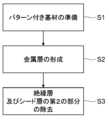
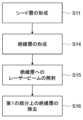
実施形態の配線基板の製造方法は、図1に示すように、パターン付き基材を準備するステップ(S1)と、金属層を形成するステップ(S2)と、絶縁層及びシード層の第2の部分を除去するステップ(S3)と、を含む。パターン付き基材を準備するステップ(S1)は、図2に示すように、シード層を形成するステップ(S11)と、絶縁層を形成するステップ(S12)と、絶縁層にレーザービーム(レーザー光)を照射するステップ(S13)と、を含んでよい。以下、各ステップを説明する。As shown in FIG. 1, the method for manufacturing a wiring board according to the embodiment includes a step of preparing a patterned substrate (S1), a step of forming a metal layer (S2), and a step of removing the insulating layer and a second portion of the seed layer (S3). As shown in FIG. 2, the step of preparing a patterned substrate (S1) may include a step of forming a seed layer (S11), a step of forming an insulating layer (S12), and a step of irradiating the insulating layer with a laser beam (laser light) (S13). Each step will be described below.
(1)パターン付き基材を準備するステップ(S1)
a)シード層の形成(S11)
まず、図3に示すように、絶縁性基材11上にシード層13を形成する。(1) Step of preparing a patterned substrate (S1)
a) Formation of seed layer (S11)
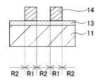
First, as shown in FIG. 3, a
絶縁性基材11としては、例えば、ガラスエポキシ樹脂基材等の樹脂及びガラスを含む基材、樹脂製の基材、ガラス製の基材等を用いることができる。絶縁性基材11に用いられる樹脂の例として、PET樹脂、PI樹脂、LCP(液晶ポリマー)、エポキシ樹脂、ABS樹脂、AS樹脂、AAS樹脂、PS樹脂、EVA樹脂、PMMA樹脂、PBT樹脂、PPS樹脂、PA樹脂、POM樹脂、PC樹脂、PP樹脂、PE樹脂、エラストマーとPPを含むポリマーアロイ樹脂、変性PPO樹脂、PTFE樹脂、ETFE樹脂等の熱可塑性樹脂、フェノール樹脂、メラミン樹脂、アミノ樹脂、不飽和ポリエステル樹脂、ポリウレタン、ジアリルフタレート、シリコーン樹脂、アルキド樹脂等の熱硬化性樹脂、エポキシ樹脂にシアネート樹脂を加えた樹脂等が挙げられる。For example, the
シード層13の材料は、導電性であり且つ後述するステップ(S3)においてシード層13をエッチングすることが可能であれば、特に限定されない。例えば、シード層13の材料は、Pt、Pd、Rh、Cu、Ag、Au、Ti、Al、Cr、Si、若しくはそれらの合金、FeSi2、CoSi2、MoSi2、WSi2、VSi2、ReSi1.75、CrSi2、NbSi2、TaSi2、TiSi2、ZrSi2等のシリサイド、特に遷移金属ケイ化物、TiO2、SnO、GeO、ITO(酸化インジウムスズ)等の導電性金属酸化物、又は導電性樹脂であってよい。後述するレーザービームを照射するステップ(S13)において、十分な厚さを有するシード層13が残存するように、シード層13は、80nm以上、好ましくは100nm以上の厚みを有してよい。また、製造コストの観点から、シード層13は、1000nm以下、好ましくは500nm以下の厚みを有してよい。 The material of the
シード層13は、絶縁性基材11の主面11aの全体に形成されてよい。シード層13は任意の方法で形成してよい。例えば、スパッタリング法等のPVD(物理気相蒸着)法、CVD(化学気相蒸着)法、無電解めっき法によりシード層13を形成することができる。あるいは、導電性粒子の分散液を絶縁性基材11の主面11aに塗布し、該分散液を固化することにより、シード層13を形成することもできる。分散液の分散媒として、加熱により揮発する液体、例えばデカノールを用いることができる。分散液は、添加剤を含んでもよい。添加剤の例として、炭素数が10~17個の直鎖脂肪酸塩が挙げられる。分散液の塗布方法は特に限定されない。例えば、ダイコート法、ディップコート法、スピンコート法が挙げられる。分散液を固化する方法は、特に限定されない。例えば、加熱により分散媒を揮発させるとともに導電性粒子を焼結することにより、分散液を固化することができる。The
シード層13は、図3に示すように、第1の部分R1、及び第1の部分R1以外の部分である第2の部分R2からなる。第1の部分R1は、実施形態の製造方法により製造される配線基板の配線パターンに応じた所定パターンを有する。As shown in FIG. 3, the
シード層13と絶縁性基材11の間の密着性を向上させるために、シード層13を形成する前に、絶縁性基材11の主面11aを表面処理してもよい。例えば、絶縁性基材11の主面11a上にプライマ等の層を形成してもよい。プライマとしては、ポリイミドやポリアミドイミド等を用いることができる。また、絶縁性基材11の主面11aを粗面化してもよい。粗面化は、レーザー照射、エッチング、デスミア処理、機械加工(研磨、研削)等により行うことができる。In order to improve adhesion between the
b)絶縁層の形成(S12)
図4に示すように、シード層13上に絶縁層16を形成する。すなわち、シード層13の第1の部分R1及び第2の部分R2上に絶縁層16を形成する。 b) Formation of an insulating layer (S12)
4, the insulating
絶縁層16の材料は、絶縁性であり且つレーザービームの照射により除去可能な材料であれば特に限定されない。絶縁層16の材料の例として、EP(エポキシ)樹脂、レゾール型PF(フェノール)樹脂、UF(ユリア)樹脂、MF(メラミン)樹脂、UP(不飽和ポリエステル)樹脂、PUR(ポリウレタン)樹脂、DAP(ジアリルフタレート)樹脂、SI(シリコーン)樹脂、ALK(アルキド)樹脂、熱硬化性PI(ポリイミド)樹脂、PPO(ポリフェニレンオキシド)樹脂、LCP(液晶ポリマー)、PTFE(ポリテトラフルオロエチレン)樹脂等の熱硬化性樹脂、及びPE(ポリエチレン)樹脂、PP(ポリプロピレン)樹脂、PS(ポリスチレン)樹脂、PET(ポリエチレンテレフタレート)樹脂、AS(アクリロニトリル-スチレン共重合体)樹脂、ABS(アクリロニトリル-ブタジエン-スチレン共重合体)樹脂、PVC(ポリ塩化ビニル)樹脂、PVDC(ポリ塩化ビニリデン)樹脂、アクリル樹脂(例えば、PMMA(ポリメタクリル酸メチル)樹脂)、ノボラック型PF樹脂等の熱可塑性樹脂が挙げられる。The material of the insulating
絶縁層16は、ダイコート法、ディップコート法、スピンコート法等の任意の方法により形成することができる。また、絶縁層16は、ドライフィルムレジストなどの絶縁性フィルムをシード層13に重ねることによって形成することもできる。The insulating
絶縁層16は、後述する金属層を形成するステップ(S2)で形成される金属層14よりも小さい厚みを有する。また、絶縁層16は、12.5μm未満、10μm以下、又は7μm以下の厚みを有してよい。それにより、後続のレーザービームを照射するステップ(S13)において、シード層13の第1の部分R1上の絶縁層16を除去し、シード層13の第1の部分R1を露出させることができる。また、絶縁層16は、十分な絶縁性を確保する観点から、0.5μm以上、特に1μm以上の厚みを有してよい。The insulating
c)絶縁層へのレーザービームの照射(S13)
シード層13の第1の部分R1上の絶縁層16にレーザービームを照射して、レーザーアブレーションによりシード層13の第1の部分R1上の絶縁層16を除去する。それにより、図5に示すように、シード層13の第1の部分R1が露出する。一方で、シード層13の第2の部分R2上の絶縁層16は残留する。絶縁層16へのレーザービームの照射は、絶縁層16をレーザービームで走査することにより行ってよい。 c) Irradiating the insulating layer with a laser beam (S13)
The insulating
レーザービームは、パルスレーザービームであってよい。また、レーザービームは、580nm以下の波長及び15ps以下のパルス幅を有してよい。後述する実施例で示すように、このようなレーザービームを用いることにより、絶縁層16を選択的に除去することができる。特に、レーザービームの波長は400nm以下であってもよい。また、レーザービームのパルス幅は1ps以下であってもよい。後述する実施例で示すように、このようなレーザービームを用いることにより、デブリの発生を低減することができる。また、400nm以下の波長を有するUVレーザーを用いることにより、絶縁層16の微細加工が容易となり、例えば、線幅と間隔(L/S)が5μm以下である配線パターンの形成が容易になる。レーザービームの波長は、10nm以上、好ましくは250nm以上であってよい。レーザービームのパルス幅は、0.1ps以上であってよい。なお、ここで、パルス幅とは、パルス持続時間と同義であり、単一のパルスにおける時間強度分布の半値全幅(FWHM)を意味する。 The laser beam may be a pulsed laser beam. The laser beam may have a wavelength of 580 nm or less and a pulse width of 15 ps or less. As shown in the examples described later, the insulating
周波数、強度、スポット径、空間強度分布、走査速度等のその他の各種のレーザービームの照射条件は、絶縁層16の材料及び厚み、シード層13の材料及び厚み、製造する配線基板の配線パターンのL/S等に応じて適宜設定してよい。例えば、レーザービームはトップハット型の空間強度分布を有してよい。それにより、絶縁層16の一部が溶融してアブレーションされずに残存することを抑制できる。Various other laser beam irradiation conditions, such as frequency, intensity, spot diameter, spatial intensity distribution, and scanning speed, may be set appropriately depending on the material and thickness of the insulating
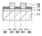
こうして、絶縁性基材11と、絶縁性基材11上に設けられた導電性のシード層13と、シード層13上に設けられた絶縁層16と、を含む、パターン付き基材10が得られる。シード層13は、絶縁層16に被覆されずに露出している第1の部分R1と、第1の部分R1以外の部分である第2の部分R2からなり、第2の部分R2の上には絶縁層16が設けられている。すなわち、シード層13の第2の部分R2は絶縁層16により被覆されている。In this way, a patterned
(2)金属層を形成するステップ(S2)
図6に示すように、シード層13の第1の部分R1上に金属層14を形成する。金属層14の材料としては、Cu、Ni、Ag、Au等が挙げられ、好ましくはCuであってよい。金属層14は、絶縁層16よりも大きい厚みを有する。また、金属層14は、例えば1~100μmの厚みを有してよい。(2) Step of forming a metal layer (S2)
6, a
金属層14の形成に用いる成膜装置50の一例を図9及び図10に示す。成膜装置50は、シード層13に対向するように配置される金属製の陽極51と、陽極51とパターン付き基材10との間に配置される樹脂膜52と、陽極51とシード層13との間に電圧を印加する電源部54と、を備える。9 and 10 show an example of a
成膜装置50は、さらに、ハウジング53を備える。ハウジング53には、陽極51と、金属層14の材料である金属のイオンを含む溶液(以下、金属溶液という)Lと、が収容される。ハウジング53は、図9に示すように、陽極51と樹脂膜52との間に、金属溶液Lが収容される空間を画成してよい。この場合、陽極51は、金属層14の材料と同じで且つ金属溶液Lに可溶な材料(例えばCu)から形成された板状部材、又は金属溶液Lに不溶な材料(例えばTi)から形成された板状部材であり得る。陽極51と樹脂膜52との間に金属溶液Lが収容される成膜装置50では、樹脂膜52とパターン付き基材10とを均一な圧力で圧接させることができるため、パターン付き基材10の全体にわたり、シード層13の第1の部分R1上に均一に金属層14を形成することが可能である。そのため、このような成膜装置50は、微細な配線パターンの形成に好適である。The
なお、図には示していないが、陽極51と樹脂膜52とが接触していてもよい。この場合、陽極51は、金属溶液Lを透過することができる多孔質体から形成されてよく、陽極51の樹脂膜52と接触する面の反対の面が、金属溶液Lが収容される空間と接触していてよい。Although not shown in the figure, the
樹脂膜52として、固体電解質膜又は多孔膜を用いることができる。A solid electrolyte membrane or a porous membrane can be used as the
固体電解質膜としては、例えば、デュポン社製のナフィオン(登録商標)等のフッ素系樹脂、炭化水素系樹脂、ポリアミック酸樹脂、旭硝子社製のセレミオン(CMV、CMD、CMFシリーズ)等の陽イオン交換機能を有する樹脂の膜が挙げられる。Examples of solid electrolyte membranes include membranes made of fluorine-based resins such as DuPont's Nafion (registered trademark), hydrocarbon-based resins, polyamic acid resins, and resins with cation exchange capabilities such as Asahi Glass's Selemion (CMV, CMD, CMF series).
多孔膜としては、例えば、ポリオレフィン鎖から構成される膜が挙げられる。ここで、ポリオレフィンとは、オレフィンの重合体(ポリマー)のすべてを指し、例えば、ポリエチレン、ポリプロピレン、又はこれらの混合物を包含する。ポリオレフィン鎖は、架橋又は非架橋であってよく、飽和又は不飽和であってよく、直鎖状でも分枝していてもよい。ポリオレフィン鎖は、置換又は非置換であってよい。ポリオレフィン鎖の好ましい実施形態として、側鎖を有さない、架橋又は非架橋のポリエチレン鎖が例示できる。多孔膜は、イオン交換性官能基を有さなくてよい。The porous membrane may be, for example, a membrane composed of polyolefin chains. Here, polyolefin refers to all polymers of olefins, including, for example, polyethylene, polypropylene, or a mixture thereof. The polyolefin chain may be crosslinked or non-crosslinked, saturated or unsaturated, and linear or branched. The polyolefin chain may be substituted or non-substituted. A preferred embodiment of the polyolefin chain is a crosslinked or non-crosslinked polyethylene chain that does not have a side chain. The porous membrane may not have an ion-exchange functional group.
多孔膜は、20~2000nm、又は27~1000nmの空孔径を有してよい。空孔径が上記範囲内であることにより、高い電流効率での金属層14の形成が可能になる。ここで、空孔径は、空孔径分布の体積平均を意味する。空孔径分布は、JIS R 1655:2003に準じる水銀圧入法により求めることができる。水銀圧入法とは、圧力をかけて水銀を開気孔に浸入させ、開気孔に浸入した水銀の体積とその時加えた圧力値の関係を求め、その結果に基づき、開気孔を円柱状と仮定してWashburnの式から開気孔の径を算出する方法である。多孔膜は、5~500s/100cm3又は10~260s/100cm3の透気度を有してよい。透気度が上記範囲内であることにより、高い電流効率での金属層14の形成が可能になる。透気度は、JIS L 1096-6-27-1A、又は、ASTM D737に準じて測定される。多孔膜は、35~90%、又は45~80%の空孔率(気孔率)を有してよい。空孔率が上記範囲内であることにより、高い電流効率での金属層14の形成が可能になる。空孔率は、単位体積中に含まれる空孔の割合である。多孔膜のみかけの密度(かさ密度)をρ1、多孔膜の真密度(多孔膜を構成するポリマーの密度)をρ2とすると、空孔率pは、p=1-ρ1/ρ2と表される。多孔膜のかさ密度ρ1は多孔膜の重量及び外寸体積から求めることができる。多孔膜の真密度はヘリウムガス置換法により測定される。多孔膜は、750~3000kgf/cm2、又は1000~2400kgf/cmでの引張強度を有してよい。引張強度が上記範囲内であることにより、より平坦な金属層14の形成が可能になる。引張強度は、JIS K 7127:1999に準じて測定される。多孔膜は、5~85%、又は15~80%の引張伸び度を有してよい。引張伸び度が上記範囲内であることにより、より平坦な金属層14の形成が可能になる。引張伸び度は、JIS C 2151、若しくは、ASTM D882に準じて測定される。多孔膜として、市販の電池用セパレータを用いることができる。市販のセパレータは固体電解質膜と比べて低コストであるとともに、さらなる低廉化が期待される。 The porous membrane may have a pore size of 20 to 2000 nm, or 27 to 1000 nm. By having the pore size within the above range, the
樹脂膜52を金属溶液Lに接触させると、金属溶液Lが樹脂膜52に浸透する。その結果、樹脂膜52は、金属溶液Lを内部に含有する。樹脂膜52は、例えば、約5μm~約200μmの厚みを有してよい。When the
金属溶液Lは、金属層14の材料である金属(例えばCu、Ni、Ag、Au等)をイオンの状態で含有する。金属溶液Lは、硝酸イオン、リン酸イオン、コハク酸イオン、硫酸イオン、ピロリン酸イオンを含んでよい。金属溶液Lは、金属の塩、例えば、硝酸塩、リン酸塩、コハク酸塩、硫酸塩、ピロリン酸塩等の水溶液であってよい。The metal solution L contains the metal (e.g., Cu, Ni, Ag, Au, etc.) that is the material of the
さらに、成膜装置50は、ハウジング53の上部に、ハウジング53を昇降させる昇降装置55を備える。昇降装置55は、例えば、油圧式又は空圧式のシリンダ、電動式のアクチュエータ、リニアガイド、モータ等を含んでよい。Furthermore, the
ハウジング53は、供給口53aと排出口53bとを有する。供給口53a及び排出口53bは、配管64を介してタンク61に接続される。配管64に接続されたポンプ62によってタンク61から送り出された金属溶液Lは、供給口53aからハウジング53内に流入し、排出口53bを介してハウジング53から排出されてタンク61に戻る。配管64には、排出口53bの下流において、圧力調整弁63が設けられる。圧力調整弁63及びポンプ62によりハウジング53内の金属溶液Lの圧力を調整することができる。The
成膜装置50は、さらに、パターン付き基材10を載置する金属台座56と、パターン付き基材10のシード層13と金属台座56とを電気的に接続するための導電部材57と、を備える。導電部材57は、パターン付き基材10の縁部の一部を覆うとともに、部分的に折り曲げられて金属台座56に接触する金属板であってよい。これにより、金属台座56が導電部材57を介してシード層13に電気的に接続される。なお、導電部材57は、パターン付き基材10に脱着可能であってよい。The
電源部54の負極は、金属台座56を介してシード層13に電気的に接続され、電源部54の正極は、陽極51に電気的に接続される。The negative electrode of the
以下のようにして、成膜装置50を用いて金属層14を形成することができる。The
図9に示すように、金属台座56上の所定位置にパターン付き基材10及び導電部材57を載置する。次いで、図10に示すように、昇降装置55によりハウジング53を所定高さまで下降させる。As shown in FIG. 9, the patterned
次いで、ポンプ62により金属溶液Lを加圧する。すると、圧力調整弁63によりハウジング53内の金属溶液Lが、所定の圧力に保たれる。また、樹脂膜52が、パターン付き基材10の表面、すなわち、シード層13の第1の部分R1及び絶縁層16の表面に倣うように変形し、シード層13の第1の部分R1及び絶縁層16の表面に接触する。それにより、樹脂膜52に含有される金属溶液Lが、シード層13の第1の部分R1及び絶縁層16の表面に接触する。樹脂膜52は、ハウジング53内の金属溶液Lの圧力で、シード層13の第1の部分R1及び絶縁層16の表面に均一に押圧される。Next, the metal solution L is pressurized by the
電源部54により、陽極51とシード層13との間に電圧を印加する。すると、シード層13の第1の部分R1に接触した金属溶液Lに含まれる金属イオンがシード層13の第1の部分R1の表面で還元され、シード層13の第1の部分R1の表面に金属が析出する。一方、絶縁層16の表面では金属イオンの還元反応は起こらないため、金属は析出しない。それにより、シード層13の第1の部分R1上に選択的に金属層14が形成される。なお、陽極51とシード層13との間に印加する電圧は、適宜設定してよい。より高い電圧を印加することにより、金属の析出速度を高めることができる。また、金属溶液Lを加熱してもよい。それにより、金属の析出速度を高めることができる。A voltage is applied between the
絶縁層16の厚みを超える所定厚みを有する金属層14が形成されるまで、陽極51とシード層13の間の電圧の印加を継続する。金属層14の厚みが絶縁層16の厚みを超えた後も、金属層14の水平方向(すなわち、金属層14の厚み方向に垂直な方向)の寸法の増加を抑制しながら、金属層14の厚みを増加させることができる(図6参照)。すなわち、金属層14は、シード層13の第1の部分R1のパターンのL/Sに対応するL/Sを有することができる。その後、陽極51とシード層13の間の電圧の印加を停止し、ポンプ62による金属溶液Lの加圧を停止する。そして、ハウジング53を所定高さまで上昇させ(図9参照)、樹脂膜52と金属層14を離間させる。金属層14が形成されたパターン付き基材10を金属台座56から取り外す。The application of voltage between the
(3)絶縁層及びシード層の第2の部分を除去するステップ(S3)
図7に示すように、絶縁層16を除去し、次いで、図8に示すように、シード層13の第2の部分R2を除去する。それにより、絶縁性基材11の主面11a上に、シード層13の第1の部分R1及び金属層14を含む、所定の配線パターンを有する配線層2が形成される。(3) removing the second portion of the insulating layer and the seed layer (S3);
As shown in Fig. 7, the insulating
絶縁層16及びシード層13の第2の部分R2は、エッチングにより除去することができる。絶縁層16及びシード層13の第2の部分R2のエッチング法は、乾式及び湿式のいずれであってもよい。乾式エッチングの例として、反応性ガスエッチング法、スパッタエッチング法、プラズマエッチング法、イオンミリング法、反応性イオンエッチング(RIE)法、反応性イオンビームエッチング法、ラジカルエッチング法、光励起エッチング法、レーザーアシストエッチング法、レーザーアブレーションエッチング法が挙げられる。反応性イオンエッチング法には、容量結合型プラズマ(CCP)、誘導結合型プラズマ(ICP)、又はマイクロ波ECR(Electron Cyclotron Resonance)プラズマを用いることができる。乾式エッチングに用いるエッチングガスは、絶縁層16及びシード層13の第2の部分R2の各材質に応じて、適宜選択してよい。エッチングガスの例として、CF4、SF6、ホウ素、塩素、HBr、BCl3が挙げられる。湿式エッチングでは、酸又はアルカリの溶液をエッチング液として用いることができる。エッチング液は絶縁層16及びシード層13の第2の部分R2の各材質に応じて、適宜選択してよい。 The insulating
以上のようにして、絶縁性基材11と、絶縁性基材11上に設けられた所定の配線パターンを有する配線層2と、を備える配線基板1が製造される。In this manner, a wiring board 1 is manufactured, which includes an insulating
本実施形態では、図9及び図10に示されるような樹脂膜52を用いた成膜装置を用いて金属層14を形成するため、絶縁層16よりも大きい厚みを有する金属層14を形成することができる。したがって、絶縁層16の厚みを低減することができる。In this embodiment, the
[変形形態]
本発明は、上記実施形態に限定されず、特許請求の範囲に記載された本発明の精神を逸脱しない範囲で、種々の設計変更を行うことができる。例えば、以下の変形が可能である。[Modifications]
The present invention is not limited to the above-described embodiment, and various design modifications can be made without departing from the spirit of the present invention as defined in the claims. For example, the following modifications are possible.
第1変形形態
本変形形態において、パターン付き基材10を準備するステップ(S1)は、図11に示すように、シード層13を形成するステップ(S11)と、絶縁層16を形成するステップ(S14)と、絶縁層16にレーザービーム(レーザー光)を照射するステップ(S15)と、シード層13の第1の部分R1上の絶縁層16を除去するステップ(S16)を含む。上述した実施形態では、絶縁層16にレーザービームを照射するステップ(S13)において、レーザーアブレーションによりシード層13の第1の部分R1上の絶縁層16を除去したが、本変形形態では、レーザービームを用いたフォトリソグラフィー(レーザーフォトリソグラフィー)により、シード層13の第1の部分R1上の絶縁層16を除去する。 11, the step (S1) of preparing the patterned
シード層13を形成するステップ(S11)は、上記実施形態のステップ(S11)と同様であるため、説明を省略する。なお、本変形形態では、シード層13の厚みは、金属層14を形成するステップ(S2)において金属層14がパターン付き基材10の全体にわたって均一に形成されるように、及び配線基板1の製造コストが抑制されるように、適宜設定してよい。The step (S11) of forming the
絶縁層16を形成するステップ(S14)では、絶縁層16として、ポジ型又はネガ型レジストの層を形成する。ポジ型又はネガ型のレジストとしては、一般的なフォトリソグラフィープロセスにおいて使用される任意のレジスト材料を使用してよい。絶縁層16の形成方法は、上記実施形態のステップ(S12)で説明した方法と同様であるため説明を省略する。なお、本変形形態では、絶縁層16の厚みは、絶縁層16が、十分な絶縁性を有するとともに、後続のステップ(S15)及びステップ(S16)でパターニング可能であるように、適宜設定してよい。In the step (S14) of forming the insulating
絶縁層16にレーザービームを照射するステップ(S15)では、シード層13の第1の部分R1上又は第2の部分R2上のいずれかの絶縁層16にレーザービームを照射する。絶縁層16がポジ型レジスト層の場合は、シード層13の第1の部分R1上の絶縁層16にレーザービームを照射し、絶縁層16がネガ型レジスト層の場合は、シード層13の第2の部分R2上の絶縁層16にレーザービームを照射する。In the step (S15) of irradiating the insulating
絶縁層16へのレーザービームの照射は、絶縁層16をレーザービームで走査することにより行ってよい。レーザービームは、パルス波であってもよいし、連続波(CW)であってもよい。レーザービームの波長、強度、スポット径、空間強度分布、走査速度、パルス幅、周波数等の各種照射条件は、絶縁層16の材料及び厚み、製造する配線基板の配線パターンのL/S等に応じて適宜設定してよい。例えば、レーザービームの波長は、10~580nmの範囲内であってよいが、これに限定されるものではない。The laser beam may be irradiated onto the insulating
次いで、シード層13の第1の部分R1上の絶縁層16を、現像液で溶解して除去する(ステップ(S16))。それにより、図5に示されるようなパターン付き基材10が得られる。現像液は、絶縁層16の材料に応じて適宜選択される。Next, the insulating
第2変形形態
本変形形態では、上述したレーザーアブレーション及びレーザーフォトリソグラフィーの代わりに、その他のパターニング法(例えば、スクリーン印刷、インクジェット印刷、転写印刷等の印刷法、フォトリソグラフィー)が、絶縁層16のパターニング法として適用される。 Second Variation In this variation, instead of the above-mentioned laser ablation and laser photolithography, other patterning methods (e.g., printing methods such as screen printing, inkjet printing, and transfer printing, and photolithography) are applied as the patterning method for the insulating
第3変形形態
本変形形態では、パターン付き基材を準備するステップ(S1)において、図12に示すようなパターン付き基材10を準備する。図12において、絶縁層16は、シード層13の第2の部分R2上に形成された主絶縁層16aと、主絶縁層16a上に形成された撥水層16bとを備える。撥水層16bの表面の水の接触角は、90度超、特に120度以上であってよい。それにより、金属層を形成するステップ(S2)において、絶縁層16上に金属が析出する可能性を低減することができる。 Third Variation In this variation, in the step (S1) of preparing a patterned substrate, a patterned
主絶縁層16aは、上記実施形態の絶縁層を形成するステップ(S12)又は上記第1変形形態の絶縁層を形成するステップ(S14)における絶縁層16の形成方法と同様にして形成することができる。The main insulating
主絶縁層16aの形成に続いて、主絶縁層16a上に撥水層16bを形成する。撥水層16bは、例えば、式SiRn-X4-n(式中、nは1、2、3、又は4を表し、Rは、それぞれ独立して、置換又は非置換のアルキル基、フェニル基、トリフルオロメチル基、アルキルシリル基、又はフルオロシリル基を表し、Xは、それぞれ独立して、水素、ハロゲン、酸素、又は窒素を表す)で表される有機シラン、式SiR3-(NR-SiR2)m-R(式中、mは1以上の整数を表し、Rは、それぞれ独立して、置換又は非置換のアルキル基、フェニル基、トリフルオロメチル基、アルキルシリル基、又はフルオロシリル基を表す。)で表される有機シラザン等を用いて形成することができる。有機シランの例として、テトラエチルシラン、テトラメチルシラン、パラアミノフェニルトリメトキシシランが挙げられる。有機シラザンの例として、ヘキサメチルジシラザン(HMDS)が挙げられる。 Following the formation of the main insulating
撥水層16bは、ディップコート法、ミストコート法、スプレーコート法、CVD法、LB(Langmuir Blogetto)法等の任意の方法により形成することができる。なお、ミストコート法とは、超音波振動子を用いて金属元素を含む原料溶液を霧化してミストを形成し、ミストを所定の表面に供給し、この表面上で熱エネルギー等によりミストを分解及び/又は反応させることにより、この表面上に金属元素を含む薄膜を形成する方法である。The water-
主絶縁層16a及び撥水層16bを備える絶縁層16は、上記実施形態及び変形形態に記載したようなレーザーアブレーション法、レーザーフォトリソグラフィー、又はその他のパターニングにより、パターニングすることができる。The insulating
パターニングされた主絶縁層16aを任意の方法で形成した後、主絶縁層16a上に選択的に撥水層16bを形成してもよい。After forming the patterned main insulating
以下、実施例により本発明を具体的に説明するが、本発明はこれらの実施例に限定されるものではない。The present invention will be described in detail below with reference to examples, but the present invention is not limited to these examples.
実施例1
絶縁性基材としてガラスエポキシ基材(ガラス繊維強化エポキシ積層材)を用意した。絶縁性基材の主面に、シード層として、500nmの厚みを有する銅膜をスパッタ法により形成した。シード層上に、絶縁層として、1.5~3μmの厚みを有する熱可塑性のノボラック樹脂の層をスピンコート法により形成した。絶縁層の所定の領域を、スポット状のレーザービーム(波長355nm、パルス幅7ps)で1回走査して、L/Sが5μmであるパターン付き基材を得た。 Example 1
A glass epoxy substrate (glass fiber reinforced epoxy laminate) was prepared as an insulating substrate. A copper film having a thickness of 500 nm was formed as a seed layer on the main surface of the insulating substrate by sputtering. A layer of thermoplastic novolac resin having a thickness of 1.5 to 3 μm was formed as an insulating layer on the seed layer by spin coating. A predetermined region of the insulating layer was scanned once with a spot-shaped laser beam (wavelength 355 nm, pulse width 7 ps) to obtain a patterned substrate with an L/S of 5 μm.
パターン付き基材の断面を、走査型電子顕微鏡(SEM)で観察し、レーザービームで走査した領域において、絶縁層が除去されてシード層が露出したこと、及び当該領域のシード層が連続膜の状態で残存したことを確認した。すなわち、絶縁層を選択的に除去することができたことが確認された(この結果は、表1中「〇」で示される)。The cross section of the patterned substrate was observed with a scanning electron microscope (SEM) and it was confirmed that in the area scanned by the laser beam, the insulating layer was removed to expose the seed layer, and that the seed layer in that area remained in the form of a continuous film. In other words, it was confirmed that the insulating layer could be selectively removed (this result is indicated by "◯" in Table 1).
上記の条件にてパターン付き基材を再度作製し、露出したシード層の表面に、金属層として5μmの厚みを有するCu層を形成した。具体的には、図9、10に示す成膜装置50を用いて、以下の条件にてCu層を形成した。A patterned substrate was prepared again under the above conditions, and a Cu layer having a thickness of 5 μm was formed as a metal layer on the exposed surface of the seed layer. Specifically, the Cu layer was formed under the following conditions using the
陰極:シード層
陽極:無酸素銅線
樹脂膜:ナフィオン(登録商標)(厚み約8μm)
金属溶液:1.0mol/Lの硫酸銅水溶液
樹脂膜をシード層に押し当てる圧力:1.0MPa
電流密度:0.23mA/cm2 Cathode: seed layer Anode: oxygen-free copper wire Resin film: Nafion (registered trademark) (thickness: approx. 8 μm)
Metal solution: 1.0 mol/L copper sulfate aqueous solution Pressure for pressing the resin film against the seed layer: 1.0 MPa
Current density: 0.23mA/cm2
次いで、CF4ガスを用いた容量結合型プラズマエッチングにより、絶縁層を除去し、さらに、金属層をマスクとしてシード層をエッチングした。それにより、シード層及び金属層からなる所定の配線パターンの配線層が、絶縁性基材上に形成された。こうして、絶縁性基材と配線層とを備える配線基板が得られた。 Next, the insulating layer was removed by capacitively coupled plasma etching usingCF4 gas, and the seed layer was further etched using the metal layer as a mask. As a result, a wiring layer having a predetermined wiring pattern composed of the seed layer and the metal layer was formed on the insulating base material. Thus, a wiring board including the insulating base material and the wiring layer was obtained.
実施例2
7μmの厚みを有する熱可塑性のドライフィルムをシード層に貼り付けることにより絶縁層を形成したこと以外は実施例1と同様にして配線基板を作製した。 Example 2
A wiring board was produced in the same manner as in Example 1, except that an insulating layer was formed by attaching a thermoplastic dry film having a thickness of 7 μm to the seed layer.
なお、パターン付き基材の断面を、SEMで観察したところ、レーザービームで走査した領域において、絶縁層が除去されてシード層が露出したこと、及び当該領域のシード層が連続膜の状態で残存したことが確認された。すなわち、絶縁層を選択的に除去することができたことが確認された。When the cross section of the patterned substrate was observed with an SEM, it was confirmed that in the area scanned by the laser beam, the insulating layer was removed to expose the seed layer, and that the seed layer in that area remained in the form of a continuous film. In other words, it was confirmed that the insulating layer could be selectively removed.
比較例1
12.5μmの厚みを有する熱硬化性のポリイミドフィルムをシード層に貼り付けることにより絶縁層を形成したこと以外は実施例1と同様にして、パターン付き基材を作製した。パターン付き基材の断面を、SEMで観察した。レーザービームで走査した領域において、絶縁層が残存し、シード層が十分に露出していないことが確認された。すなわち、絶縁層を選択的に除去することができなかった(この結果は、表1中「×」で示される)。 Comparative Example 1
A patterned substrate was prepared in the same manner as in Example 1, except that an insulating layer was formed by attaching a thermosetting polyimide film having a thickness of 12.5 μm to the seed layer. The cross section of the patterned substrate was observed with an SEM. It was confirmed that the insulating layer remained in the region scanned with the laser beam, and the seed layer was not sufficiently exposed. That is, the insulating layer could not be selectively removed (this result is indicated by "x" in Table 1).
実施例3、4
シード層の厚みを表1に記載の通りとしたこと以外は実施例1と同様にして、配線基板を作製した。 Examples 3 and 4
A wiring board was produced in the same manner as in Example 1, except that the thickness of the seed layer was as shown in Table 1.
なお、パターン付き基材の断面を、SEMで観察したところ、レーザービームで走査した領域において、絶縁層が除去されてシード層が露出したこと、及び当該領域のシード層が連続膜の状態で残存したことが確認された。すなわち、絶縁層を選択的に除去することができたことが確認された。When the cross section of the patterned substrate was observed with an SEM, it was confirmed that in the area scanned by the laser beam, the insulating layer was removed to expose the seed layer, and that the seed layer in that area remained in the form of a continuous film. In other words, it was confirmed that the insulating layer could be selectively removed.
比較例2、3
シード層の厚みを表1に記載の通りとしたこと以外は実施例1と同様にして、パターン付き基材を作製した。パターン付き基材の断面を、SEMで観察した。レーザービームで走査した領域において、絶縁層だけでなくシード層も除去され、十分な厚さを有するシード層は残存しなかった。すなわち、絶縁層を選択的に除去することができなかった。 Comparative Examples 2 and 3
A patterned substrate was prepared in the same manner as in Example 1, except that the thickness of the seed layer was as shown in Table 1. The cross section of the patterned substrate was observed with an SEM. In the area scanned with the laser beam, not only the insulating layer but also the seed layer was removed, and no seed layer having a sufficient thickness remained. In other words, the insulating layer could not be selectively removed.
実施例5
絶縁層に照射するレーザービームの波長及びパルス幅を表1に記載の通りとしたこと以外は実施例1と同様にして、配線基板を作製した。 Example 5
A wiring board was produced in the same manner as in Example 1, except that the wavelength and pulse width of the laser beam irradiated onto the insulating layer were as shown in Table 1.
なお、パターン付き基材の断面を、SEMで観察したところ、レーザービームで走査した領域において、絶縁層が除去されてシード層が露出したこと、及び当該領域のシード層が連続膜の状態で残存したことが確認された。すなわち、絶縁層を選択的に除去することができたことが確認された。When the cross section of the patterned substrate was observed with an SEM, it was confirmed that in the area scanned by the laser beam, the insulating layer was removed to expose the seed layer, and that the seed layer in that area remained in the form of a continuous film. In other words, it was confirmed that the insulating layer could be selectively removed.
実施例6
絶縁層に照射するレーザービームの波長及びパルス幅を表1に記載の通りとしたこと以外は実施例1と同様にして、配線基板を作製した。 Example 6
A wiring board was produced in the same manner as in Example 1, except that the wavelength and pulse width of the laser beam irradiated onto the insulating layer were as shown in Table 1.
なお、パターン付き基材の断面を、SEMで観察したところ、レーザービームで走査した領域において、絶縁層が除去されてシード層が露出したこと、及び当該領域のシード層が連続膜の状態で残存したことが確認された。すなわち、絶縁層を選択的に除去することができたことが確認された。ただし、パターン付基材には、絶縁層の溶融固化物であるデブリが見られた(この結果は、表1中「△」で示される)。When the cross section of the patterned substrate was observed with an SEM, it was confirmed that in the area scanned by the laser beam, the insulating layer was removed to expose the seed layer, and that the seed layer in that area remained in the form of a continuous film. In other words, it was confirmed that the insulating layer could be selectively removed. However, debris, which was a molten and solidified product of the insulating layer, was found on the patterned substrate (this result is indicated by "△" in Table 1).
比較例4
絶縁層に照射するレーザービームの波長及びパルス幅を表1に記載の通りとしたこと以外は実施例2と同様にして、パターン付き基材を作製した。パターン付き基材の断面を、SEMで観察した。レーザービームで走査した領域において、絶縁層が残存し、シード層が十分に露出していないことが確認された。すなわち、絶縁層を選択的に除去することができなかった。 Comparative Example 4
A patterned substrate was prepared in the same manner as in Example 2, except that the wavelength and pulse width of the laser beam irradiated to the insulating layer were as shown in Table 1. The cross section of the patterned substrate was observed with an SEM. It was confirmed that the insulating layer remained in the region scanned with the laser beam, and the seed layer was not sufficiently exposed. In other words, the insulating layer could not be selectively removed.
実施例7
絶縁層として、1.5~3μmの厚みを有する熱硬化性のエポキシ樹脂の層をスピンコート法により形成したこと、及び絶縁層に照射するレーザービームのパルス幅を表1に記載の通りとしたこと以外は実施例1と同様にして配線基板を作製した。 Example 7
A wiring board was produced in the same manner as in Example 1, except that a layer of thermosetting epoxy resin having a thickness of 1.5 to 3 μm was formed as the insulating layer by a spin coating method, and the pulse width of the laser beam irradiated to the insulating layer was set as shown in Table 1.
なお、パターン付き基材の断面を、SEMで観察したところ、レーザービームで走査した領域において、絶縁層が除去されてシード層が露出したこと、及び当該領域のシード層が連続膜の状態で残存したことが確認された。すなわち、絶縁層を選択的に除去することができたことが確認された。When the cross section of the patterned substrate was observed with an SEM, it was confirmed that in the area scanned by the laser beam, the insulating layer was removed to expose the seed layer, and that the seed layer in that area remained in the form of a continuous film. In other words, it was confirmed that the insulating layer could be selectively removed.
実施例8
絶縁層として、1.5~3μmの厚みを有する熱硬化性のポリイミド樹脂の層をスピンコート法により形成したこと以外は実施例7と同様にして配線基板を作製した。 Example 8
A wiring board was produced in the same manner as in Example 7, except that a layer of thermosetting polyimide resin having a thickness of 1.5 to 3 μm was formed as the insulating layer by spin coating.
なお、パターン付き基材の断面を、SEMで観察したところ、レーザービームで走査した領域において、絶縁層が除去されてシード層が露出したこと、及び当該領域のシード層が連続膜の状態で残存したことが確認された。すなわち、絶縁層を選択的に除去することができたことが確認された。When the cross section of the patterned substrate was observed with an SEM, it was confirmed that in the area scanned by the laser beam, the insulating layer was removed to expose the seed layer, and that the seed layer in that area remained in the form of a continuous film. In other words, it was confirmed that the insulating layer could be selectively removed.
実施例9
絶縁層に照射するレーザービームの波長を表1に記載の通りとしたこと以外は実施例1と同様にして、配線基板を作製した。 Example 9
A wiring board was produced in the same manner as in Example 1, except that the wavelength of the laser beam irradiated onto the insulating layer was as shown in Table 1.
なお、パターン付き基材の断面を、SEMで観察したところ、レーザービームで走査した領域において、絶縁層が除去されてシード層が露出したこと、及び当該領域のシード層が連続膜の状態で残存したことが確認された。すなわち、絶縁層を選択的に除去することができたことが確認された。When the cross section of the patterned substrate was observed with an SEM, it was confirmed that in the area scanned by the laser beam, the insulating layer was removed to expose the seed layer, and that the seed layer in that area remained in the form of a continuous film. In other words, it was confirmed that the insulating layer could be selectively removed.
実施例10
レーザーフォトリソグラフィーにより所定の領域の絶縁層を消失させたこと以外は、実施例1と同様にして、配線基板を作製した。なお、レーザーフォトリソグラフィーは、具体的には、絶縁層の所定の領域をスポット状の連続波レーザービーム(波長436nm)で1回走査して露光し、次いで、現像液で所定の領域の絶縁層を溶解させて除去することにより行った。また、Cu層を形成した後、絶縁層を除去する前に、断面SEM観察を行った。断面SEM写真を図13に示す。絶縁層の厚みを超える厚みを有するCu層が形成されたことが確認された。Cu層は、いずれの高さ(厚み方向の位置)においても略一定の幅(水平方向の寸法)を有していた。 Example 10
A wiring board was produced in the same manner as in Example 1, except that the insulating layer in a predetermined region was removed by laser photolithography. Specifically, the laser photolithography was performed by scanning a predetermined region of the insulating layer once with a spot-shaped continuous wave laser beam (wavelength 436 nm) to expose it, and then dissolving and removing the insulating layer in the predetermined region with a developing solution. In addition, after the Cu layer was formed, cross-sectional SEM observation was performed before removing the insulating layer. A cross-sectional SEM photograph is shown in FIG. 13. It was confirmed that a Cu layer having a thickness exceeding the thickness of the insulating layer was formed. The Cu layer had a substantially constant width (horizontal dimension) at any height (position in the thickness direction).

1:配線基板、2:配線層、10:パターン付き基材、11:絶縁性基材、R1:第1の部分、R2:第2の部分、13:シード層、14:金属層、16:絶縁層、50:成膜装置、51:陽極、52:樹脂膜、L:金属イオンを含む溶液(金属溶液)
1: wiring substrate, 2: wiring layer, 10: patterned substrate, 11: insulating substrate, R1: first portion, R2: second portion, 13: seed layer, 14: metal layer, 16: insulating layer, 50: film forming device, 51: anode, 52: resin film, L: solution containing metal ions (metal solution)
Claims (2)
Translated fromJapanese(a)パターン付き基材を準備するステップであって、
ここで、前記パターン付き基材が、
前記絶縁性基材と、
前記絶縁性基材上に設けられた、前記配線パターンに応じた所定パターンを有する第1の部分及び第1の部分以外の部分である第2の部分からなる、80nm以上の厚さを有する導電性のシード層と、
前記シード層の第2の部分上に設けられた、12.5μm未満の厚さを有する絶縁層と、を備え、
前記絶縁層が、前記シード層の第2の部分上に設けられた主絶縁層、及び前記主絶縁層上に設けられた撥水層を備え、前記撥水層の表面の水の接触角が90度超であり、
前記ステップ(a)が、
前記シード層の第1の部分及び第2の部分上に、前記絶縁層を形成することと、
第1の部分上の前記絶縁層に、355nm以下の波長及び7ps以下のパルス幅を有するレーザービームを照射して、第1の部分上の前記絶縁層を除去することと、
を含む、ステップと、
(b)前記シード層の第1の部分上に金属層を形成するステップであって、前記金属層の上面が前記絶縁層の上面より高く、
ここで、前記パターン付き基材と陽極との間に、金属イオンを含む固体電解質膜を配置し、前記固体電解質膜と前記シード層とを圧接させながら、前記陽極と前記シード層との間に電圧を印加する、ステップと、
(c)前記絶縁層、及び前記シード層の第2の部分を除去するステップと、
を含む、方法。 A method for manufacturing a wiring board including an insulating base material and a wiring layer having a predetermined wiring pattern provided on the insulating base material, comprising:
(a) providing a patterned substrate, comprising:
wherein the patterned substrate is
The insulating substrate;
a conductive seed layer having a thickness of 80 nm or more provided on the insulating base material, the conductive seed layer including a first portion having a predetermined pattern corresponding to the wiring pattern and a second portion other than the first portion;
an insulating layer disposed on the second portion of the seed layer and having a thickness of less than 12.5 μm;
the insulating layer comprises a main insulating layer provided on the second portion of the seed layer and a water-repellent layer provided on the main insulating layer, the water-repellent layer having a surface with a water contact angle of greater than 90 degrees;
The step (a)
forming the insulating layer over the first and second portions of the seed layer;
irradiating the insulating layer on a first portion with a laser beam having a wavelength of355 nm or less and a pulse width of 7 ps or less to remove the insulating layer on the first portion;
and
(b) forming a metal layer on a first portion of the seed layer, the top surface of the metal layer being higher than the top surface of the insulating layer;
a step of disposing a solid electrolyte film containing metal ions between the patterned substrate and an anode, and applying a voltage between the anode and the seed layer while pressing the solid electrolyte film and the seed layer together;
(c) removing the insulating layer and a second portion of the seed layer;
A method comprising:
Priority Applications (7)
| Application Number | Priority Date | Filing Date | Title |
|---|---|---|---|
| JP2021025668AJP7596842B2 (en) | 2021-02-19 | 2021-02-19 | Method for manufacturing a wiring board |
| KR1020220002557AKR102598378B1 (en) | 2021-02-19 | 2022-01-07 | Method for producing wiring substrate |
| EP22150683.5AEP4048037A1 (en) | 2021-02-19 | 2022-01-10 | Method for manufacturing wiring board |
| CN202210049035.9ACN114980536B (en) | 2021-02-19 | 2022-01-17 | Method for manufacturing wiring substrate |
| TW111102163ATW202234958A (en) | 2021-02-19 | 2022-01-19 | Method for manufacturing wiring board |
| US17/672,067US11785721B2 (en) | 2021-02-19 | 2022-02-15 | Method for manufacturing wiring board |
| BR102022002973-3ABR102022002973A2 (en) | 2021-02-19 | 2022-02-16 | METHOD TO MANUFACTURE WIRING BOARD |
Applications Claiming Priority (1)
| Application Number | Priority Date | Filing Date | Title |
|---|---|---|---|
| JP2021025668AJP7596842B2 (en) | 2021-02-19 | 2021-02-19 | Method for manufacturing a wiring board |
Publications (2)
| Publication Number | Publication Date |
|---|---|
| JP2022127486A JP2022127486A (en) | 2022-08-31 |
| JP7596842B2true JP7596842B2 (en) | 2024-12-10 |
Family
ID=79288063
Family Applications (1)
| Application Number | Title | Priority Date | Filing Date |
|---|---|---|---|
| JP2021025668AActiveJP7596842B2 (en) | 2021-02-19 | 2021-02-19 | Method for manufacturing a wiring board |
Country Status (7)
| Country | Link |
|---|---|
| US (1) | US11785721B2 (en) |
| EP (1) | EP4048037A1 (en) |
| JP (1) | JP7596842B2 (en) |
| KR (1) | KR102598378B1 (en) |
| CN (1) | CN114980536B (en) |
| BR (1) | BR102022002973A2 (en) |
| TW (1) | TW202234958A (en) |
Citations (10)
| Publication number | Priority date | Publication date | Assignee | Title |
|---|---|---|---|---|
| JP2002321079A (en) | 2001-02-21 | 2002-11-05 | Sumitomo Heavy Ind Ltd | Laser processing method |
| JP2005202412A (en) | 2004-01-16 | 2005-07-28 | Fujifilm Electronic Imaging Ltd | Method of forming mask pattern on substrate |
| WO2006033315A1 (en) | 2004-09-24 | 2006-03-30 | Ibiden Co., Ltd. | Plating method and plating apparatus |
| JP2014121734A (en) | 2008-10-23 | 2014-07-03 | Sumitomo Electric Ind Ltd | Laser processing method |
| WO2015098870A1 (en) | 2013-12-27 | 2015-07-02 | 日立化成株式会社 | Photosensitive resin composition, photosensitive element, method for forming resist pattern, and method for manufacturing printed circuit board |
| US20160090660A1 (en) | 2006-06-07 | 2016-03-31 | Actus Potentia, Inc. | Method for focused electric-field imprinting for micron and sub-micron patterns on wavy or planar surfaces |
| JP2016125087A (en) | 2014-12-26 | 2016-07-11 | トヨタ自動車株式会社 | Metal coating deposition apparatus and deposition method |
| JP2017112223A (en) | 2015-12-16 | 2017-06-22 | 三菱瓦斯化学株式会社 | Laser drilling method |
| JP2017133085A (en) | 2016-01-29 | 2017-08-03 | トヨタ自動車株式会社 | Metal film deposition method |
| JP2019062195A (en) | 2017-09-27 | 2019-04-18 | 株式会社タムラ製作所 | Method of forming pattern of solder resist film, and method of manufacturing electronic substrate |
Family Cites Families (21)
| Publication number | Priority date | Publication date | Assignee | Title |
|---|---|---|---|---|
| US4432855A (en)* | 1982-09-30 | 1984-02-21 | International Business Machines Corporation | Automated system for laser mask definition for laser enhanced and conventional plating and etching |
| US4877644A (en)* | 1988-04-12 | 1989-10-31 | Amp Incorporated | Selective plating by laser ablation |
| US20020197492A1 (en)* | 2001-06-25 | 2002-12-26 | Ling Hao | Selective plating on plastic components |
| JP4665531B2 (en) | 2005-01-27 | 2011-04-06 | 日立電線株式会社 | Wiring board manufacturing method |
| JP2008258483A (en) | 2007-04-06 | 2008-10-23 | Hitachi Cable Ltd | Method for manufacturing printed wiring board |
| JP2011138869A (en)* | 2009-12-28 | 2011-07-14 | Ngk Spark Plug Co Ltd | Method of manufacturing multilayer wiring substrate, and multilayer wiring substrate |
| US20140014401A1 (en)* | 2012-07-12 | 2014-01-16 | Taiwan Green Point Enterprises Co., Ltd. | Circuit device and method for making the same |
| JPWO2014065207A1 (en)* | 2012-10-26 | 2016-09-08 | 太陽誘電ケミカルテクノロジー株式会社 | Mesh structure and manufacturing method thereof |
| JP6217465B2 (en)* | 2014-03-06 | 2017-10-25 | 富士通株式会社 | Wiring structure manufacturing method, wiring structure, and electronic device using the same |
| JP6265163B2 (en)* | 2015-04-02 | 2018-01-24 | トヨタ自動車株式会社 | Wiring pattern forming method and wiring pattern forming etching processing apparatus |
| JP6665990B2 (en) | 2015-06-02 | 2020-03-13 | 住友電工プリントサーキット株式会社 | Base material for high-frequency printed wiring board, high-frequency printed wiring board, method for manufacturing base material for high-frequency printed wiring board, and method for manufacturing high-frequency printed wiring board |
| JP2017011148A (en)* | 2015-06-24 | 2017-01-12 | 住友ベークライト株式会社 | Method for manufacturing wiring board |
| JP2017011147A (en)* | 2015-06-24 | 2017-01-12 | 住友ベークライト株式会社 | Wiring board and method for manufacturing wiring board |
| JP2017017168A (en)* | 2015-06-30 | 2017-01-19 | 住友ベークライト株式会社 | Method for manufacturing wiring board |
| KR102081191B1 (en)* | 2016-06-24 | 2020-02-26 | 에이피시스템 주식회사 | A Method for Manufacturing a Fine Metal Mask Using Electroplating |
| US10849233B2 (en)* | 2017-07-10 | 2020-11-24 | Catlam, Llc | Process for forming traces on a catalytic laminate |
| US11266025B2 (en)* | 2017-11-21 | 2022-03-01 | Qualtec Co., Ltd. | Electronic-component manufacturing method and electronic components |
| JP6967039B2 (en)* | 2019-06-28 | 2021-11-17 | 帝人株式会社 | Plating diaphragm, plating method and plating equipment |
| JP7238712B2 (en) | 2019-09-18 | 2023-03-14 | トヨタ自動車株式会社 | Wiring board manufacturing method and wiring board |
| US11705332B2 (en)* | 2020-03-30 | 2023-07-18 | Taiwan Semiconductor Manufacturing Co., Ltd. | Photoresist layer surface treatment, cap layer, and method of forming photoresist pattern |
| JP7424218B2 (en) | 2020-06-12 | 2024-01-30 | トヨタ自動車株式会社 | Manufacturing method of wiring board |
- 2021
- 2021-02-19JPJP2021025668Apatent/JP7596842B2/enactiveActive
- 2022
- 2022-01-07KRKR1020220002557Apatent/KR102598378B1/enactiveActive
- 2022-01-10EPEP22150683.5Apatent/EP4048037A1/enactivePending
- 2022-01-17CNCN202210049035.9Apatent/CN114980536B/enactiveActive
- 2022-01-19TWTW111102163Apatent/TW202234958A/enunknown
- 2022-02-15USUS17/672,067patent/US11785721B2/enactiveActive
- 2022-02-16BRBR102022002973-3Apatent/BR102022002973A2/ennot_activeApplication Discontinuation
Patent Citations (10)
| Publication number | Priority date | Publication date | Assignee | Title |
|---|---|---|---|---|
| JP2002321079A (en) | 2001-02-21 | 2002-11-05 | Sumitomo Heavy Ind Ltd | Laser processing method |
| JP2005202412A (en) | 2004-01-16 | 2005-07-28 | Fujifilm Electronic Imaging Ltd | Method of forming mask pattern on substrate |
| WO2006033315A1 (en) | 2004-09-24 | 2006-03-30 | Ibiden Co., Ltd. | Plating method and plating apparatus |
| US20160090660A1 (en) | 2006-06-07 | 2016-03-31 | Actus Potentia, Inc. | Method for focused electric-field imprinting for micron and sub-micron patterns on wavy or planar surfaces |
| JP2014121734A (en) | 2008-10-23 | 2014-07-03 | Sumitomo Electric Ind Ltd | Laser processing method |
| WO2015098870A1 (en) | 2013-12-27 | 2015-07-02 | 日立化成株式会社 | Photosensitive resin composition, photosensitive element, method for forming resist pattern, and method for manufacturing printed circuit board |
| JP2016125087A (en) | 2014-12-26 | 2016-07-11 | トヨタ自動車株式会社 | Metal coating deposition apparatus and deposition method |
| JP2017112223A (en) | 2015-12-16 | 2017-06-22 | 三菱瓦斯化学株式会社 | Laser drilling method |
| JP2017133085A (en) | 2016-01-29 | 2017-08-03 | トヨタ自動車株式会社 | Metal film deposition method |
| JP2019062195A (en) | 2017-09-27 | 2019-04-18 | 株式会社タムラ製作所 | Method of forming pattern of solder resist film, and method of manufacturing electronic substrate |
Non-Patent Citations (1)
| Title |
|---|
| Kock-Yee LAW,"Definitions for Hydrophilicity, Hydrophobicity, and Superhydrophobicity: Getting the Basics Right",The Journal of Physical Chemistry Letters,2014年02月20日,Vol. 5, No. 4,p.686-688,DOI: 10.1021/jz402762h |
Also Published As
| Publication number | Publication date |
|---|---|
| KR20220118903A (en) | 2022-08-26 |
| US20220272847A1 (en) | 2022-08-25 |
| CN114980536A (en) | 2022-08-30 |
| TW202234958A (en) | 2022-09-01 |
| US11785721B2 (en) | 2023-10-10 |
| BR102022002973A2 (en) | 2022-08-23 |
| EP4048037A1 (en) | 2022-08-24 |
| KR102598378B1 (en) | 2023-11-03 |
| JP2022127486A (en) | 2022-08-31 |
| CN114980536B (en) | 2024-03-08 |
Similar Documents
| Publication | Publication Date | Title |
|---|---|---|
| JP7209685B2 (en) | Multilayer circuit board with intervening layer and conductive paste | |
| US11490528B2 (en) | Method for manufacturing wiring board, and wiring board | |
| CN111094621A (en) | Semi-additive method for printed circuit boards | |
| KR20060125918A (en) | Modified carbon products, their use in fuel cells and similar devices and related methods | |
| EP1479114A2 (en) | Ion exchange system structure with a microtextured surface, method of manufacture, and method of use thereof | |
| TW200902304A (en) | Method for producing metal-coated base laminates | |
| US10849233B2 (en) | Process for forming traces on a catalytic laminate | |
| US20210392753A1 (en) | Method for producing wiring substrate | |
| JP7596842B2 (en) | Method for manufacturing a wiring board | |
| EP3501242A1 (en) | Plasma etched catalytic laminate with traces and vias | |
| KR102548962B1 (en) | Method for producing wiring substrate | |
| US11696410B2 (en) | Method for producing wiring substrate | |
| JP2022012256A (en) | Wiring board manufacturing method |
Legal Events
| Date | Code | Title | Description |
|---|---|---|---|
| A621 | Written request for application examination | Free format text:JAPANESE INTERMEDIATE CODE: A621 Effective date:20230223 | |
| A977 | Report on retrieval | Free format text:JAPANESE INTERMEDIATE CODE: A971007 Effective date:20231211 | |
| A131 | Notification of reasons for refusal | Free format text:JAPANESE INTERMEDIATE CODE: A131 Effective date:20240130 | |
| A521 | Request for written amendment filed | Free format text:JAPANESE INTERMEDIATE CODE: A523 Effective date:20240326 | |
| A131 | Notification of reasons for refusal | Free format text:JAPANESE INTERMEDIATE CODE: A131 Effective date:20240625 | |
| A521 | Request for written amendment filed | Free format text:JAPANESE INTERMEDIATE CODE: A523 Effective date:20240822 | |
| TRDD | Decision of grant or rejection written | ||
| A01 | Written decision to grant a patent or to grant a registration (utility model) | Free format text:JAPANESE INTERMEDIATE CODE: A01 Effective date:20241029 | |
| A61 | First payment of annual fees (during grant procedure) | Free format text:JAPANESE INTERMEDIATE CODE: A61 Effective date:20241111 | |
| R150 | Certificate of patent or registration of utility model | Ref document number:7596842 Country of ref document:JP Free format text:JAPANESE INTERMEDIATE CODE: R150 |