JP7596459B2 - Display device - Google Patents
Display deviceDownload PDFInfo
- Publication number
- JP7596459B2 JP7596459B2JP2023116442AJP2023116442AJP7596459B2JP 7596459 B2JP7596459 B2JP 7596459B2JP 2023116442 AJP2023116442 AJP 2023116442AJP 2023116442 AJP2023116442 AJP 2023116442AJP 7596459 B2JP7596459 B2JP 7596459B2
- Authority
- JP
- Japan
- Prior art keywords
- layer
- transistor
- thin film
- electrode
- oxide semiconductor
- Prior art date
- Legal status (The legal status is an assumption and is not a legal conclusion. Google has not performed a legal analysis and makes no representation as to the accuracy of the status listed.)
- Active
Links
Images


Classifications
- H—ELECTRICITY
- H10—SEMICONDUCTOR DEVICES; ELECTRIC SOLID-STATE DEVICES NOT OTHERWISE PROVIDED FOR
- H10D—INORGANIC ELECTRIC SEMICONDUCTOR DEVICES
- H10D86/00—Integrated devices formed in or on insulating or conducting substrates, e.g. formed in silicon-on-insulator [SOI] substrates or on stainless steel or glass substrates
- H10D86/40—Integrated devices formed in or on insulating or conducting substrates, e.g. formed in silicon-on-insulator [SOI] substrates or on stainless steel or glass substrates characterised by multiple TFTs
- H—ELECTRICITY
- H10—SEMICONDUCTOR DEVICES; ELECTRIC SOLID-STATE DEVICES NOT OTHERWISE PROVIDED FOR
- H10D—INORGANIC ELECTRIC SEMICONDUCTOR DEVICES
- H10D30/00—Field-effect transistors [FET]
- H10D30/60—Insulated-gate field-effect transistors [IGFET]
- H10D30/67—Thin-film transistors [TFT]
- H10D30/6704—Thin-film transistors [TFT] having supplementary regions or layers in the thin films or in the insulated bulk substrates for controlling properties of the device
- H—ELECTRICITY
- H10—SEMICONDUCTOR DEVICES; ELECTRIC SOLID-STATE DEVICES NOT OTHERWISE PROVIDED FOR
- H10D—INORGANIC ELECTRIC SEMICONDUCTOR DEVICES
- H10D30/00—Field-effect transistors [FET]
- H10D30/60—Insulated-gate field-effect transistors [IGFET]
- H10D30/67—Thin-film transistors [TFT]
- H10D30/674—Thin-film transistors [TFT] characterised by the active materials
- H10D30/6755—Oxide semiconductors, e.g. zinc oxide, copper aluminium oxide or cadmium stannate
- H—ELECTRICITY
- H10—SEMICONDUCTOR DEVICES; ELECTRIC SOLID-STATE DEVICES NOT OTHERWISE PROVIDED FOR
- H10D—INORGANIC ELECTRIC SEMICONDUCTOR DEVICES
- H10D64/00—Electrodes of devices having potential barriers
- H10D64/60—Electrodes characterised by their materials
- H10D64/62—Electrodes ohmically coupled to a semiconductor
- H—ELECTRICITY
- H10—SEMICONDUCTOR DEVICES; ELECTRIC SOLID-STATE DEVICES NOT OTHERWISE PROVIDED FOR
- H10D—INORGANIC ELECTRIC SEMICONDUCTOR DEVICES
- H10D86/00—Integrated devices formed in or on insulating or conducting substrates, e.g. formed in silicon-on-insulator [SOI] substrates or on stainless steel or glass substrates
- H10D86/01—Manufacture or treatment
- H10D86/021—Manufacture or treatment of multiple TFTs
- H10D86/0212—Manufacture or treatment of multiple TFTs comprising manufacture, treatment or coating of substrates
- H—ELECTRICITY
- H10—SEMICONDUCTOR DEVICES; ELECTRIC SOLID-STATE DEVICES NOT OTHERWISE PROVIDED FOR
- H10D—INORGANIC ELECTRIC SEMICONDUCTOR DEVICES
- H10D86/00—Integrated devices formed in or on insulating or conducting substrates, e.g. formed in silicon-on-insulator [SOI] substrates or on stainless steel or glass substrates
- H10D86/40—Integrated devices formed in or on insulating or conducting substrates, e.g. formed in silicon-on-insulator [SOI] substrates or on stainless steel or glass substrates characterised by multiple TFTs
- H10D86/421—Integrated devices formed in or on insulating or conducting substrates, e.g. formed in silicon-on-insulator [SOI] substrates or on stainless steel or glass substrates characterised by multiple TFTs having a particular composition, shape or crystalline structure of the active layer
- H10D86/423—Integrated devices formed in or on insulating or conducting substrates, e.g. formed in silicon-on-insulator [SOI] substrates or on stainless steel or glass substrates characterised by multiple TFTs having a particular composition, shape or crystalline structure of the active layer comprising semiconductor materials not belonging to the Group IV, e.g. InGaZnO
- H—ELECTRICITY
- H10—SEMICONDUCTOR DEVICES; ELECTRIC SOLID-STATE DEVICES NOT OTHERWISE PROVIDED FOR
- H10D—INORGANIC ELECTRIC SEMICONDUCTOR DEVICES
- H10D86/00—Integrated devices formed in or on insulating or conducting substrates, e.g. formed in silicon-on-insulator [SOI] substrates or on stainless steel or glass substrates
- H10D86/40—Integrated devices formed in or on insulating or conducting substrates, e.g. formed in silicon-on-insulator [SOI] substrates or on stainless steel or glass substrates characterised by multiple TFTs
- H10D86/441—Interconnections, e.g. scanning lines
- H—ELECTRICITY
- H10—SEMICONDUCTOR DEVICES; ELECTRIC SOLID-STATE DEVICES NOT OTHERWISE PROVIDED FOR
- H10D—INORGANIC ELECTRIC SEMICONDUCTOR DEVICES
- H10D86/00—Integrated devices formed in or on insulating or conducting substrates, e.g. formed in silicon-on-insulator [SOI] substrates or on stainless steel or glass substrates
- H10D86/40—Integrated devices formed in or on insulating or conducting substrates, e.g. formed in silicon-on-insulator [SOI] substrates or on stainless steel or glass substrates characterised by multiple TFTs
- H10D86/60—Integrated devices formed in or on insulating or conducting substrates, e.g. formed in silicon-on-insulator [SOI] substrates or on stainless steel or glass substrates characterised by multiple TFTs wherein the TFTs are in active matrices
Landscapes
- Thin Film Transistor (AREA)
- Liquid Crystal (AREA)
- Electroluminescent Light Sources (AREA)
- Metal-Oxide And Bipolar Metal-Oxide Semiconductor Integrated Circuits (AREA)
- Devices For Indicating Variable Information By Combining Individual Elements (AREA)
- Electrodes Of Semiconductors (AREA)
- Shift Register Type Memory (AREA)
Description
Translated fromJapanese本発明は、酸化物半導体を用いる半導体装置及びその作製方法に関する。The present invention relates to a semiconductor device using an oxide semiconductor and a method for manufacturing the same.
なお、本明細書中において半導体装置とは、半導体特性を利用することで機能しうる装置
全般を指し、表示装置などの電気光学装置、半導体回路及び電子機器は全て半導体装置で
ある。In this specification, the term "semiconductor device" refers to any device that can function by utilizing semiconductor characteristics, and electro-optical devices such as display devices, semiconductor circuits, and electronic devices are all classified as semiconductor devices.
透光性を有する金属酸化物が半導体装置において利用されている。例えば、酸化インジウ
ム錫(ITO)などの導電性を備える金属酸化物(以下、酸化物導電体という)は、液晶
ディスプレイなどの表示装置で必要とされる透明電極材料として適用されている。Metal oxides having light-transmitting properties are used in semiconductor devices. For example, metal oxides having electrical conductivity (hereinafter, referred to as oxide conductors), such as indium tin oxide (ITO), are used as transparent electrode materials required for display devices such as liquid crystal displays.
加えて、半導体特性を示す材料としても透光性を有する金属酸化物が注目されている。例
えば、In-Ga-Zn-O系酸化物などは、液晶ディスプレイなどの表示装置で必要と
される半導体材料に適用することが期待されている。特に、薄膜トランジスタ(以下、T
FTという)のチャネル層に適用することが期待されている。In addition, metal oxides with light-transmitting properties are also attracting attention as materials that exhibit semiconductor properties. For example, In-Ga-Zn-O oxides are expected to be used as semiconductor materials required for display devices such as liquid crystal displays. In particular, thin film transistors (TFTs)
It is expected that this technology will be applied to the channel layer of a semiconductor laser (called a FT).
半導体特性を備えた金属酸化物(以下、酸化物半導体という)を適用したTFTは、低温
プロセスによって作製することが可能である。そのため、表示装置などで用いられるアモ
ルファスシリコンを代替又は凌駕する材料としての期待が高まっている。TFTs that use metal oxides with semiconducting properties (hereinafter referred to as oxide semiconductors) can be fabricated using low-temperature processes. Therefore, there are high expectations for oxide semiconductors as a material that can replace or surpass amorphous silicon used in display devices and the like.
また、酸化物導電体及び酸化物半導体は、共に透光性を有する。そのため、これらを用い
てTFTを構成することによって、透光性を有するTFTを作製することができる(例え
ば、非特許文献1参照)。In addition, since both an oxide conductor and an oxide semiconductor have light-transmitting properties, a light-transmitting TFT can be manufactured by using these materials (see, for example, Non-Patent Document 1).
また、酸化物半導体を適用したTFTは、電界効果移動度が高い。そのため、当該TFT
を用いて、表示装置などの駆動回路を構成することもできる(例えば、非特許文献2参照
)。In addition, the TFT using the oxide semiconductor has a high field effect mobility.
It is also possible to configure a driving circuit for a display device or the like using the above (see, for example, Non-Patent Document 2).
本発明の一態様は、半導体装置の製造コストを低減することを課題の一とする。An object of one embodiment of the present invention is to reduce the manufacturing cost of a semiconductor device.
本発明の一態様は、半導体装置の開口率を向上することを課題の一とする。An object of one embodiment of the present invention is to improve the aperture ratio of a semiconductor device.
本発明の一態様は、半導体装置の表示部を高精細化することを課題の一とする。An object of one embodiment of the present invention is to improve the resolution of the display portion of a semiconductor device.
本発明の一態様は、高速駆動が可能な半導体装置を提供することを課題の一とする。An object of one embodiment of the present invention is to provide a semiconductor device capable of high-speed operation.
本発明の一態様は、同一基板上に駆動回路部と、表示部とを有し、当該駆動回路部は、ソ
ース電極(ソース電極層ともいう)及びドレイン電極(ドレイン電極層ともいう)が金属
によって構成され且つチャネル層が酸化物半導体によって構成された駆動回路用TFTと
、金属によって構成された駆動回路用配線とを有し、当該表示部は、ソース電極及びドレ
イン電極が酸化物導電体によって構成され且つ半導体層が酸化物半導体によって構成され
た画素用TFTと、酸化物導電体によって構成された表示部用配線とを有する表示装置で
ある。One embodiment of the present invention is a display device that has a driver circuit unit and a display unit over the same substrate, the driver circuit unit having a driver circuit TFT whose source electrode (also referred to as a source electrode layer) and a drain electrode (also referred to as a drain electrode layer) are made of metal and whose channel layer is made of an oxide semiconductor, and driver circuit wiring made of metal, and the display unit has a pixel TFT whose source electrode and drain electrode are made of an oxide conductor and whose semiconductor layer is made of an oxide semiconductor, and display unit wiring made of an oxide conductor.
なお、非特許文献1には、具体的なTFTの作製工程及び表示装置を構成する他の素子(
例えば、容量素子など)の構造などは開示されていない。また、同一基板上に駆動回路と
、透光性を有するTFTとを作製する記載などもない。In addition, Non-Patent
For example, the structure of a capacitor element is not disclosed. In addition, there is no description of forming a driver circuit and a light-transmitting TFT on the same substrate.
本発明の一態様の半導体装置は、同一基板上において、駆動回路用TFTを有する駆動回
路部、及び画素用TFTを有する表示部が作製される。そのため、当該半導体装置の製造
コストを低減することができる。In the semiconductor device of one embodiment of the present invention, a driver circuit portion having a driver circuit TFT and a display portion having a pixel TFT are manufactured over the same substrate, which allows reduction in manufacturing cost of the semiconductor device.
また、本発明の一態様の半導体装置は、表示部に、ソース電極及びドレイン電極が酸化物
導電体によって構成され且つ半導体層が酸化物半導体によって構成された画素用TFTと
、酸化物導電体によって構成された表示部用配線とを有する。つまり、当該半導体装置は
、画素用TFT及び画素用配線が形成された領域を開口部とすることができる。そのため
、当該半導体装置の開口率を向上させることができる。In addition, the semiconductor device according to one embodiment of the present invention includes a pixel TFT having a source electrode and a drain electrode made of an oxide conductor and a semiconductor layer made of an oxide semiconductor in a display portion, and a display portion wiring made of an oxide conductor. In other words, the semiconductor device can have an opening in the region where the pixel TFT and the pixel wiring are formed. Therefore, the aperture ratio of the semiconductor device can be improved.
また、本発明の一態様の半導体装置は、表示部に、ソース電極及びドレイン電極が酸化物
導電体によって構成され且つ半導体層が酸化物半導体によって構成された画素用TFTと
、酸化物導電体によって構成された表示部用配線とを有する。つまり、当該半導体装置は
、画素用TFTのサイズに制限されることなく画素サイズを設計することができる。その
ため、当該半導体装置の表示部を高精細化することができる。In addition, the semiconductor device of one embodiment of the present invention includes a pixel TFT having a source electrode and a drain electrode made of an oxide conductor and a semiconductor layer made of an oxide semiconductor in a display portion, and a display portion wiring made of an oxide conductor. In other words, the pixel size of the semiconductor device can be designed without being limited by the size of the pixel TFT. Therefore, the display portion of the semiconductor device can have high resolution.
また、本発明の一態様の半導体装置は、駆動回路部に、ソース電極及びドレイン電極が金
属によって構成され且つチャネル層が酸化物半導体によって構成された駆動回路用TFT
と、金属によって構成された駆動回路用配線とを有する。つまり、当該半導体装置は、高
い電界効果移動度を示すTFTと、抵抗の低い配線とによって駆動回路が構成される。そ
のため、当該半導体装置を高速駆動が可能な半導体装置とすることができる。In addition, the semiconductor device according to one embodiment of the present invention includes a driver circuit TFT having a source electrode and a drain electrode made of a metal and a channel layer made of an oxide semiconductor.
and wiring for a driving circuit made of metal. That is, in the semiconductor device, the driving circuit is composed of TFTs exhibiting high field effect mobility and wiring with low resistance. Therefore, the semiconductor device can be a semiconductor device capable of high speed operation.
また、本明細書中で用いる酸化物半導体は、InMO3(ZnO)m(m>0)で表記さ
れる薄膜を形成し、その薄膜を酸化物半導体層として用いた薄膜トランジスタを作製する
。なお、Mは、Ga、Fe、Ni、Mn及びCoから選ばれた一の金属元素または複数の
金属元素を示す。例えばMとして、Gaの場合があることの他、GaとNiまたはGaと
Feなど、Ga以外の上記金属元素が含まれる場合がある。また、上記酸化物半導体にお
いて、Mとして含まれる金属元素の他に、不純物元素としてFe、Niその他の遷移金属
元素、または該遷移金属の酸化物が含まれているものがある。本明細書においては、In
MO3(ZnO)m(m>0)で表記される構造の酸化物半導体層のうち、MとしてGa
を含む構造の酸化物半導体をIn-Ga-Zn-O系酸化物半導体とよび、その薄膜をI
n-Ga-Zn-O系非単結晶膜とも呼ぶ。In addition, the oxide semiconductor used in this specification is a thin film represented by InMO3 (ZnO)m (m>0), and a thin film transistor is fabricated using the thin film as an oxide semiconductor layer. Note that M represents one or more metal elements selected from Ga, Fe, Ni, Mn, and Co. For example, M may be Ga, or may contain the above metal elements other than Ga, such as Ga and Ni or Ga and Fe. In addition to the metal element contained as M, some of the above oxide semiconductors contain Fe, Ni or other transition metal elements, or oxides of the transition metals, as impurity elements. In this specification, In
In the oxide semiconductor layer having a structure represented by MO3 (ZnO)m (m>0), M is Ga.
The oxide semiconductor having the structure containing In—Ga—Zn—O is called an In—Ga—Zn—O-based oxide semiconductor, and the thin film of the oxide semiconductor is called an In—Ga—Zn—O-based oxide semiconductor.
It is also called an n-Ga-Zn-O based non-single crystal film.
また、酸化物半導体層に適用する酸化物半導体として上記の他にも、In-Sn-Zn-
O系、In-Al-Zn-O系、Sn-Ga-Zn-O系、Al-Ga-Zn-O系、S
n-Al-Zn-O系、In-Zn-O系、Sn-Zn-O系、Al-Zn-O系、In
-O系、Sn-O系、Zn-O系の酸化物半導体を適用することができる。また上記酸化
物半導体層に酸化珪素を含ませてもよい。酸化物半導体層に結晶化を阻害する酸化珪素(
SiOx(X>0))を含ませることで、製造プロセス中において酸化物半導体層の形成
後に加熱処理した場合に、結晶化してしまうのを抑制することができる。なお、酸化物半
導体層は非晶質な状態であることが好ましく、一部結晶化していてもよい。In addition to the above, the oxide semiconductor layer can be formed using In—Sn—Zn—
O-based, In-Al-Zn-O-based, Sn-Ga-Zn-O-based, Al-Ga-Zn-O-based, S
n-Al-Zn-O system, In-Zn-O system, Sn-Zn-O system, Al-Zn-O system, In
A —O-based, Sn—O-based, or Zn—O-based oxide semiconductor can be used. The oxide semiconductor layer may contain silicon oxide.
By including SiOx (X>0), crystallization can be suppressed when a heat treatment is performed after the formation of the oxide semiconductor layer in a manufacturing process. Note that the oxide semiconductor layer is preferably in an amorphous state, and may be partially crystallized.
酸化物半導体は、好ましくはInを含有する酸化物半導体、さらに好ましくは、In、及
びGaを含有する酸化物半導体である。酸化物半導体層をI型(真性)とするため、脱水
化または脱水素化は有効である。The oxide semiconductor is preferably an oxide semiconductor containing In, more preferably an oxide semiconductor containing In and Ga. In order to make the oxide semiconductor layer i-type (intrinsic), dehydration or dehydrogenation is effective.
窒素、または希ガス(アルゴン、ヘリウムなど)の不活性気体雰囲気下、或いは減圧下で
の加熱処理を行った場合、酸化物半導体層は加熱処理により酸素欠乏型となって低抵抗化
、即ちN型化(N-化など)させ、その後、酸化物半導体層に接する酸化物絶縁膜の形成
を行うことにより酸化物半導体層を酸素過剰な状態とすることで高抵抗化、即ちI型化さ
せている。これにより、電気特性が良好で信頼性のよい薄膜トランジスタを有する半導体
装置を作製し、提供することが可能となる。When heat treatment is performed in an inert gas atmosphere of nitrogen or a rare gas (such as argon or helium) or under reduced pressure, the oxide semiconductor layer becomes oxygen-deficient and has low resistance, that is, becomes N-type (such asN- ), and then, by forming an oxide insulating film in contact with the oxide semiconductor layer, the oxide semiconductor layer becomes oxygen-excessive and has high resistance, that is, becomes I-type. This makes it possible to manufacture and provide a semiconductor device including a thin film transistor with good electrical characteristics and high reliability.
脱水化または脱水素化は、窒素、または希ガス(アルゴン、ヘリウムなど)の不活性気体
雰囲気下、或いは減圧下での350℃以上、好ましくは400℃以上基板の歪み点未満の
加熱処理を行い、酸化物半導体層の含有水分などの不純物を低減する。The dehydration or dehydrogenation is performed by heat treatment at 350° C. or higher, preferably 400° C. or higher and lower than the strain point of the substrate, in an inert gas atmosphere of nitrogen or a rare gas (such as argon or helium) or under reduced pressure, to reduce impurities such as moisture contained in the oxide semiconductor layer.
脱水化または脱水素化の条件は、脱水化または脱水素化後の酸化物半導体層に対して昇温
脱離ガス分析法(TDS:Thermal Desorption Spectrosc
opy)で450℃まで測定を行っても水の2つのピーク、少なくとも300℃付近に現
れる1つのピークが検出されない程度の熱処理条件とする。従って、脱水化または脱水素
化が行われた酸化物半導体層を用いた薄膜トランジスタに対してTDSで450℃まで測
定を行っても少なくとも300℃付近に現れる水のピークは検出されない。The dehydration or dehydrogenation conditions were as follows: the oxide semiconductor layer after the dehydration or dehydrogenation was subjected to thermal desorption spectroscopy (TDS).
The heat treatment conditions are set such that two water peaks and at least one water peak appearing near 300° C. are not detected even when measurement is performed up to 450° C. by TDS. Thus, even when measurement is performed up to 450° C. by TDS on a thin film transistor using an oxide semiconductor layer that has been dehydrated or dehydrogenated, at least a water peak appearing near 300° C. is not detected.
そして、酸化物半導体層に対して脱水化または脱水素化を行う加熱温度Tから、脱水化ま
たは脱水素化を行った同じ炉で大気に触れさせることなく冷却することにより、酸化物半
導体層に水または水素を再び混入させないことが重要である。脱水化または脱水素化を行
い、酸化物半導体層を低抵抗化、即ちN型化(N-、N+など)させた後、高抵抗化させ
てI型とした酸化物半導体層を用いて薄膜トランジスタを作製すると、薄膜トランジスタ
のしきい値電圧値をプラスとすることができ、所謂ノーマリーオフのスイッチング素子を
実現できる。薄膜トランジスタのゲート電圧が0Vにできるだけ近い正のしきい値電圧で
チャネルが形成されることが半導体装置(表示装置)には望ましい。なお、薄膜トランジ
スタのしきい値電圧値がマイナスであると、ゲート電圧が0Vでもソース電極とドレイン
電極の間に電流が流れる、所謂ノーマリーオンとなりやすい。アクティブマトリクス型の
表示装置においては、回路を構成する薄膜トランジスタの電気特性が重要であり、この電
気特性が表示装置の性能を左右する。特に、薄膜トランジスタの電気特性のうち、しきい
値電圧(Vth)が重要である。電界効果移動度が高くともしきい値電圧値が高い、或い
はしきい値電圧値がマイナスであると、回路として制御することが困難である。しきい値
電圧値が高く、しきい値電圧の絶対値が大きい薄膜トランジスタの場合には、駆動電圧が
低い状態ではTFTとしてのスイッチング機能を果たすことができず、負荷となる恐れが
ある。nチャネル型の薄膜トランジスタの場合、ゲート電圧に正の電圧を印加してはじめ
てチャネルが形成されて、ドレイン電流が流れ出すトランジスタが望ましい。駆動電圧を
高くしないとチャネルが形成されないトランジスタや、負の電圧状態でもチャネルが形成
されてドレイン電流が流れるトランジスタは、回路に用いる薄膜トランジスタとしては不
向きである。It is important to prevent water or hydrogen from being mixed again into the oxide semiconductor layer by cooling the oxide semiconductor layer from the heating temperature T at which the dehydration or dehydrogenation is performed in the same furnace as the dehydration or dehydrogenation without exposing the oxide semiconductor layer to the air. When the oxide semiconductor layer is dehydrated or dehydrogenated to reduce its resistance, that is, to become an N-type (N-, N+, etc.), and then the oxide semiconductor layer is made high-resistance and made an I-type to manufacture a thin film transistor, the threshold voltage value of the thin film transistor can be made positive, and a so-called normally-off switching element can be realized. It is desirable for a semiconductor device (display device) that the channel is formed at a positive threshold voltage of the thin film transistor that is as close as possible to 0V. Note that if the threshold voltage value of the thin film transistor is negative, a current flows between the source electrode and the drain electrode even when the gate voltage is 0V, which is a so-called normally-on state. In an active matrix display device, the electrical characteristics of the thin film transistor that constitutes the circuit are important, and these electrical characteristics affect the performance of the display device. In particular, the threshold voltage (Vth) is important among the electrical characteristics of the thin film transistor. Even if the field effect mobility is high, if the threshold voltage value is high or the threshold voltage value is negative, it is difficult to control it as a circuit. In the case of a thin film transistor with a high threshold voltage value and a large absolute value of the threshold voltage, it cannot perform the switching function as a TFT when the driving voltage is low, and there is a risk that it will become a load. In the case of an n-channel thin film transistor, a transistor in which a channel is formed and a drain current flows only when a positive voltage is applied to the gate voltage is desirable. A transistor in which a channel is not formed unless the driving voltage is high, or a transistor in which a channel is formed and a drain current flows even in a negative voltage state, is not suitable as a thin film transistor to be used in a circuit.
また、加熱温度Tから下げるガス雰囲気は、加熱温度Tまで昇温したガス雰囲気と異なる
ガス雰囲気に切り替えてもよい。例えば、脱水化または脱水素化を行った同じ炉で大気に
触れさせることなく、炉の中を高純度の酸素ガスまたはN2Oガス、超乾燥エア(露点が
-40℃以下、好ましくは-60℃以下)で満たして冷却を行う。The gas atmosphere for lowering the heating temperature T may be changed to a gas atmosphere different from the gas atmosphere for raising the temperature to the heating temperature T. For example, cooling is performed in the same furnace used for dehydration or dehydrogenation without exposing the material to the air, by filling the furnace with high-purity oxygen gas or N2 O gas or ultra-dry air (dew point of −40° C. or lower, preferably −60° C. or lower).
脱水化または脱水素化を行う加熱処理によって膜中の含有水分を低減させた後、水分を含
まない雰囲気(露点が-40℃以下、好ましくは-60℃以下)下で徐冷(または冷却)
した酸化物半導体膜を用いて、薄膜トランジスタの電気特性を向上させるとともに、量産
性と高性能の両方を備えた薄膜トランジスタを実現する。The moisture content in the film is reduced by a heat treatment for dehydration or dehydrogenation, and then the film is gradually cooled (or cooled) in a moisture-free atmosphere (dew point of -40°C or less, preferably -60°C or less).
By using the oxide semiconductor film, the electrical characteristics of a thin film transistor are improved and a thin film transistor that is both mass-producible and high-performance is realized.
本明細書では、窒素、または希ガス(アルゴン、ヘリウムなど)の不活性気体雰囲気下、
或いは減圧下での加熱処理を脱水化または脱水素化のための加熱処理と呼ぶ。本明細書で
は、この加熱処理によってH2として脱離させていることのみを脱水素化と呼んでいるわ
けではなく、H、OHなどを脱離することを含めて脱水化または脱水素化と便宜上呼ぶこ
ととする。In this specification, the method is carried out under an inert gas atmosphere of nitrogen or a rare gas (argon, helium, etc.),
Alternatively, the heat treatment under reduced pressure is called a heat treatment for dehydration or dehydrogenation. In this specification, dehydrogenation does not only refer to the desorption ofH2 by this heat treatment, but also includes the desorption of H, OH, etc., for convenience.
窒素、または希ガス(アルゴン、ヘリウムなど)の不活性気体雰囲気下、或いは減圧下で
の加熱処理を行った場合、酸化物半導体層は加熱処理により酸素欠乏型となって低抵抗化
、即ちN型化(N-化など)させる。その後、ドレイン電極層と重なる領域が酸素欠乏型
である高抵抗ドレイン領域(HRD領域とも呼ぶ)として形成される。When heat treatment is performed in an inert gas atmosphere of nitrogen or a rare gas (such as argon or helium) or under reduced pressure, the oxide semiconductor layer becomes oxygen-deficient and has low resistance, that is, becomes N-type (such as N- type). After that, a region overlapping with the drain electrode layer is formed as an oxygen-deficient high-resistance drain region (also referred to as an HRD region).
具体的には、高抵抗ドレイン領域のキャリア濃度は、1×10¹⁷/cm3以上の範囲内
であり、少なくともチャネル形成領域のキャリア濃度(1×10¹⁷/cm3未満)より
も高い領域である。なお、本明細書のキャリア濃度は、室温にてHall効果測定から求
めたキャリア濃度の値を指す。Specifically, the carrier concentration of the high-resistance drain region is in the range of 1×10¹⁷ /cm3 or more, and is at least higher than the carrier concentration of the channel formation region (less than 1×10¹⁷ /cm3 ). Note that the carrier concentration in this specification refers to the value of the carrier concentration determined by Hall effect measurement at room temperature.
また、酸化物半導体層と金属材料からなるドレイン電極層の間に低抵抗ドレイン領域(L
RN領域とも呼ぶ)を形成してもよい。具体的には、低抵抗ドレイン領域のキャリア濃度
は、高抵抗ドレイン領域(HRD領域)よりも大きく、例えば1×10²⁰/cm3以上
1×10²¹/cm3以下の範囲内である。In addition, a low-resistance drain region (L) is formed between the oxide semiconductor layer and the drain electrode layer made of a metal material.
Specifically, the carrier concentration of the low-resistance drain region is higher than that of the high-resistance drain region (HRD region), and is within a range of, for example, 1×10²⁰ /cm3 to 1×10²¹ /cm3 .
そして、脱水化または脱水素化した酸化物半導体層の少なくとも一部を酸素過剰な状態と
することで、高抵抗化、即ちI型化させてチャネル形成領域を形成する。なお、脱水化ま
たは脱水素化した酸化物半導体層を酸素過剰な状態とする処理としては、脱水化または脱
水素化した酸化物半導体層に接する酸化物絶縁膜のスパッタ法での成膜、または酸化物絶
縁膜成膜後の加熱処理、または酸化物絶縁膜成膜後の酸素を含む雰囲気での加熱処理、ま
たは酸化物絶縁膜成膜後の不活性ガス雰囲気下で加熱した後に酸素雰囲気で冷却する処理
、または酸化物絶縁膜成膜後の不活性ガス雰囲気下で加熱した後に超乾燥エア(露点が-
40℃以下、好ましくは-60℃以下)で冷却する処理などによって行う。At least a part of the dehydrated or dehydrogenated oxide semiconductor layer is made to have an oxygen-excess state, thereby making the oxide semiconductor layer highly resistant, that is, an I-type, and forming a channel formation region. Note that the treatment for making the dehydrated or dehydrogenated oxide semiconductor layer into an oxygen-excess state can be performed by forming an oxide insulating film in contact with the dehydrated or dehydrogenated oxide semiconductor layer by a sputtering method, by heat treatment after the oxide insulating film is formed, by heat treatment in an atmosphere containing oxygen after the oxide insulating film is formed, by heating in an inert gas atmosphere after the oxide insulating film is formed and then cooling in an oxygen atmosphere, or by heating in an inert gas atmosphere after the oxide insulating film is formed and then cooling in an oxygen atmosphere.
This is carried out by a cooling treatment at a temperature of 40° C. or less, preferably −60° C. or less.
また、脱水化または脱水素化した酸化物半導体層の少なくとも一部(ゲート電極層と重な
る部分)をチャネル形成領域とするため、選択的に酸素過剰な状態とすることで、高抵抗
化、即ちI型化させることもできる。脱水化または脱水素化した酸化物半導体層上に接し
てTiなどの金属電極からなるソース電極層やドレイン電極層を形成し、ソース電極層や
ドレイン電極層に重ならない露出領域を選択的に酸素過剰な状態としてチャネル形成領域
を形成することができる。選択的に酸素過剰な状態とする場合、ソース電極層に重なる第
1の高抵抗ドレイン領域と、ドレイン電極層に重なる第2の高抵抗ドレイン領域とが形成
され、第1の高抵抗ドレイン領域と第2の高抵抗ドレイン領域との間の領域がチャネル形
成領域となる。即ち、チャネル形成領域がソース電極層及びドレイン電極層の間に自己整
合的に形成される。In addition, at least a part of the dehydrated or dehydrogenated oxide semiconductor layer (a part overlapping with the gate electrode layer) is made into a channel formation region, so that the oxide semiconductor layer can be selectively made into an oxygen-excess state to have high resistance, that is, an I-type oxide semiconductor layer. A source electrode layer or a drain electrode layer made of a metal electrode such as Ti is formed in contact with the dehydrated or dehydrogenated oxide semiconductor layer, and an exposed region not overlapping with the source electrode layer or the drain electrode layer is selectively made into an oxygen-excess state to form a channel formation region. When the oxygen-excess state is selectively set, a first high-resistance drain region overlapping with the source electrode layer and a second high-resistance drain region overlapping with the drain electrode layer are formed, and a region between the first high-resistance drain region and the second high-resistance drain region becomes a channel formation region. That is, the channel formation region is formed in a self-aligned manner between the source electrode layer and the drain electrode layer.
これにより、電気特性が良好で信頼性のよい薄膜トランジスタを有する半導体装置を作製
し、提供することが可能となる。As a result, it is possible to manufacture and provide a semiconductor device having a thin film transistor with good electrical characteristics and high reliability.
なお、ドレイン電極層(及びソース電極層)と重畳した酸化物半導体層において高抵抗ド
レイン領域を形成することにより、駆動回路を形成した際の信頼性の向上を図ることがで
きる。具体的には、高抵抗ドレイン領域を形成することで、ドレイン電極層から高抵抗ド
レイン領域、チャネル形成領域にかけて、導電性を段階的に変化させうるような構造とす
ることができる。そのため、ドレイン電極層に高電源電位VDDを供給する配線に接続し
て動作させる場合、ゲート電極層とドレイン電極層との間に高電界が印加されても高抵抗
ドレイン領域がバッファとなり局所的な高電界が印加されず、トランジスタの耐圧を向上
させた構成とすることができる。Note that by forming a high-resistance drain region in the oxide semiconductor layer overlapping with the drain electrode layer (and the source electrode layer), reliability can be improved when a driver circuit is formed. Specifically, by forming the high-resistance drain region, a structure can be formed in which conductivity can be changed stepwise from the drain electrode layer to the high-resistance drain region and the channel formation region. Therefore, when the drain electrode layer is connected to a wiring that supplies a high power supply potential VDD and operated, even if a high electric field is applied between the gate electrode layer and the drain electrode layer, the high-resistance drain region serves as a buffer to prevent a local high electric field from being applied, and a structure in which the withstand voltage of the transistor is improved can be obtained.
また、金属材料からなるドレイン電極層(及びソース電極層)と酸化物半導体層との間に
低抵抗ドレイン領域(LRN領域とも呼ぶ)を形成してもよく、低抵抗ドレイン領域(L
RN領域とも呼ぶ)を形成することによって、よりトランジスタの耐圧を向上させた構成
とすることができる。In addition, a low-resistance drain region (also referred to as an LRN region) may be formed between the drain electrode layer (and the source electrode layer) made of a metal material and the oxide semiconductor layer.
By forming a second region (also referred to as an RN region), the withstand voltage of the transistor can be further improved.
また、ドレイン電極層(及びソース電極層)と重畳した酸化物半導体層において高抵抗ド
レイン領域を形成することにより、駆動回路を形成した際のチャネル形成領域でのリーク
電流の低減を図ることができる。具体的には、高抵抗ドレイン領域を形成することで、ド
レイン電極層とソース電極層との間に流れるトランジスタのリーク電流の経路として、ド
レイン電極層、ドレイン電極層側の高抵抗ドレイン領域、チャネル形成領域、ソース電極
層側の高抵抗ドレイン領域、ソース電極層の順となる。このときチャネル形成領域では、
ドレイン電極層側の低抵抗N型領域よりチャネル領域に流れるリーク電流を、トランジス
タがオフ時に高抵抗となるゲート絶縁層とチャネル形成領域の界面近傍に集中させること
ができ、バックチャネル部(ゲート電極層から離れているチャネル形成領域の表面の一部
)でのリーク電流を低減することができる。Furthermore, by forming a high-resistance drain region in the oxide semiconductor layer overlapping with the drain electrode layer (and the source electrode layer), leakage current in the channel formation region can be reduced when a driver circuit is formed. Specifically, by forming the high-resistance drain region, the path of leakage current of the transistor flowing between the drain electrode layer and the source electrode layer is in the order of the drain electrode layer, the high-resistance drain region on the drain electrode layer side, the channel formation region, the high-resistance drain region on the source electrode layer side, and the source electrode layer. In this case, in the channel formation region,
The leakage current flowing from the low-resistance N-type region on the drain electrode layer side to the channel region can be concentrated in the vicinity of the interface between the gate insulating layer, which becomes highly resistive when the transistor is off, and the channel formation region, thereby reducing the leakage current in the back channel portion (a part of the surface of the channel formation region that is away from the gate electrode layer).
また、ソース電極層に重なる第1の高抵抗ドレイン領域と、ドレイン電極層に重なる第2
の高抵抗ドレイン領域は、ゲート電極層の幅にもよるが、ゲート電極層の一部とゲート絶
縁層を介して重なり、より効果的にドレイン電極層の端部近傍の電界強度を緩和させるこ
とができる。A first high-resistance drain region overlapping the source electrode layer and a second high-resistance drain region overlapping the drain electrode layer.
The high-resistance drain region overlaps with a part of the gate electrode layer via the gate insulating layer, depending on the width of the gate electrode layer, and can more effectively reduce the electric field intensity near the end of the drain electrode layer.
すなわち、本発明の一態様である半導体装置は、同一基板上に第1の薄膜トランジスタを
有する駆動回路と第2の薄膜トランジスタを有する画素部を有している。第2の薄膜トラ
ンジスタは、基板上にボトムゲート電極と、ボトムゲート電極上にゲート絶縁層と、ゲー
ト絶縁層上に酸化物半導体層と、酸化物半導体層の一部と接する第2のチャネル保護層と
、第2のチャネル保護層及び酸化物半導体層上にソース電極及びドレイン電極と、第2の
チャネル保護層上に画素電極層を有している。さらに、第2の薄膜トランジスタのボトム
ゲート電極、ゲート絶縁層、酸化物半導体層、ソース電極、ドレイン電極、第2のチャネ
ル保護層、及び画素電極層は透光性を有している。また、第1の薄膜トランジスタのソー
ス電極及びドレイン電極は、第2の薄膜トランジスタのソース電極及びドレイン電極と材
料が異なり、第2の薄膜トランジスタのソース電極及び前記ドレイン電極よりも低抵抗の
導電材料であることを特徴とする。That is, a semiconductor device according to one embodiment of the present invention includes a driver circuit having a first thin film transistor and a pixel portion having a second thin film transistor over the same substrate. The second thin film transistor includes a bottom gate electrode over the substrate, a gate insulating layer over the bottom gate electrode, an oxide semiconductor layer over the gate insulating layer, a second channel protective layer in contact with a part of the oxide semiconductor layer, a source electrode and a drain electrode over the second channel protective layer and the oxide semiconductor layer, and a pixel electrode layer over the second channel protective layer. The bottom gate electrode, the gate insulating layer, the oxide semiconductor layer, the source electrode, the drain electrode, the second channel protective layer, and the pixel electrode layer of the second thin film transistor have light-transmitting properties. The source electrode and the drain electrode of the first thin film transistor are made of a different material from the source electrode and the drain electrode of the second thin film transistor and are made of a conductive material having a lower resistance than the source electrode and the drain electrode of the second thin film transistor.
また、本発明の一態様は、上述の半導体装置において、第1の薄膜トランジスタは、第1
の薄膜トランジスタの酸化物半導体層の一部と接する第1のチャネル保護層と、第1のチ
ャネル保護層及び酸化物半導体層上にソース電極及びドレイン電極を有することを特徴と
する半導体装置である。Further, one embodiment of the present invention is a semiconductor device comprising:
the semiconductor device further comprising: a first channel protection layer in contact with a part of an oxide semiconductor layer of the thin film transistor; and a source electrode and a drain electrode over the first channel protection layer and the oxide semiconductor layer.
また、本発明の一態様は、上述の半導体装置において、第1の薄膜トランジスタは、第1
の薄膜トランジスタの酸化物半導体層の一部と接する第1のチャネル保護層と、第1のチ
ャネル保護層及び酸化物半導体層上にソース電極及びドレイン電極を有する。さらに、チ
ャネル形成領域上に第1のチャネル保護層を介してバックゲート電極を有することを特徴
とする半導体装置である。Further, one embodiment of the present invention is a semiconductor device comprising:
the thin film transistor further includes a first channel protection layer in contact with a part of an oxide semiconductor layer of the thin film transistor, a source electrode and a drain electrode over the first channel protection layer and the oxide semiconductor layer, and a backgate electrode over a channel formation region with the first channel protection layer interposed therebetween.
また、本発明の一態様は、上述の半導体装置において、第1のチャネル保護層と第2のチ
ャネル保護層は、同じ透光性を有する絶縁材料であることを特徴とする半導体装置である
。Another embodiment of the present invention is a semiconductor device in which the first channel protective layer and the second channel protective layer are made of the same light-transmitting insulating material in any of the above-described semiconductor devices.
また、本発明の一態様は、上述の半導体装置において、第1の薄膜トランジスタのソース
電極及びドレイン電極は、Al、Cr、Cu、Ta、Ti、Mo、Wから選ばれた元素を
主成分とする膜、若しくはそれらの合金膜とを組み合わせた積層膜からなることを特徴と
する半導体装置である。Another aspect of the present invention is the semiconductor device, wherein a source electrode and a drain electrode of the first thin film transistor are made of a film containing an element selected from Al, Cr, Cu, Ta, Ti, Mo, and W as a main component, or a stacked film combining an element selected from Al, Cr, Cu, Ta, Ti, Mo, and W with an alloy film thereof.
また、本発明の一態様は、上述の半導体装置において、前記第2の薄膜トランジスタのソ
ース電極層、ドレイン電極層、及び画素電極層は、酸化インジウム、酸化インジウム酸化
スズ合金、酸化インジウム酸化亜鉛合金、または酸化亜鉛であることを特徴とする半導体
装置である。Another embodiment of the present invention is the semiconductor device, in which a source electrode layer, a drain electrode layer, and a pixel electrode layer of the second thin film transistor are made of indium oxide, an alloy of indium oxide and tin oxide, an alloy of indium oxide and zinc oxide, or zinc oxide.
また、本発明の一態様は、上述の半導体装置において、さらに同一基板上に容量部を有し
、容量部は、容量配線及び該容量配線と重なる容量電極を有し、容量配線及び容量電極は
透光性を有する半導体装置である。Another embodiment of the present invention is a semiconductor device including the above-described semiconductor device, further including a capacitance portion over the same substrate. The capacitance portion includes a capacitance wiring and a capacitance electrode overlapping with the capacitance wiring, and the capacitance wiring and the capacitance electrode have light-transmitting properties.
安定した電気特性を有する薄膜トランジスタを作製し、提供することができる。よって、
電気特性が良好で信頼性のよい薄膜トランジスタを有する半導体装置を提供することがで
きる。A thin film transistor having stable electrical characteristics can be manufactured and provided.
A semiconductor device having a thin film transistor with good electrical characteristics and high reliability can be provided.
実施の形態について、図面を用いて詳細に説明する。但し、本発明は以下の説明に限定さ
れず、本発明の趣旨およびその範囲から逸脱することなくその形態および詳細を様々に変
更し得ることは当業者であれば容易に理解される。従って、本発明は以下に示す実施の形
態の記載内容に限定して解釈されるものではない。なお、以下に説明する発明の構成にお
いて、同一部分または同様な機能を有する部分には同一の符号を異なる図面間で共通して
用い、その繰り返しの説明は省略する。The embodiments will be described in detail with reference to the drawings. However, the present invention is not limited to the following description, and it will be easily understood by those skilled in the art that the form and details of the present invention can be modified in various ways without departing from the spirit and scope of the present invention. Therefore, the present invention should not be interpreted as being limited to the description of the embodiments shown below. In the configuration of the invention described below, the same parts or parts having similar functions are denoted by the same reference numerals in different drawings, and repeated explanations thereof will be omitted.
(実施の形態1)
本実施の形態は、本発明の一態様である薄膜トランジスタおよびその作製方法について説
明する。(Embodiment 1)
In this embodiment, a thin film transistor which is one embodiment of the present invention and a manufacturing method thereof will be described.
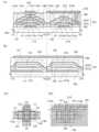
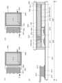
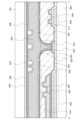
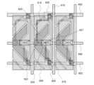
図1(A)に、本発明の一態様である薄膜トランジスタ141及び142の断面図を示す
。薄膜トランジスタ141及び142は同一の基板100上に形成され、どちらもボトム
ゲート型の薄膜トランジスタである。薄膜トランジスタ141は駆動回路に配置され、薄
膜トランジスタ142は画素に配置されている。1A shows a cross-sectional view of
図1(C1)は駆動回路に配置されるチャネルストップ型の薄膜トランジスタ141の平
面図であり、図1(A)は図1(C1)の線C1-C2における断面図である。また、図
1(B)は、図1(C1)の線C3-C4における断面図である。Fig. 1C1 is a plan view of a channel stop type
また、図1(C2)は画素に配置されるチャネルストップ型の薄膜トランジスタ142の
平面図であり、図1(A)は図1(C2)の線D1-D2における断面図である。また、
図1(B)は、図1(C2)の線D3-D4における断面図である。FIG. 1C2 is a plan view of a channel stop type
FIG. 1B is a cross-sectional view taken along line D3-D4 in FIG.
薄膜トランジスタ141は、基板100上に設けた、第1のボトムゲート電極111と、
ゲート絶縁膜102と、第3の酸化物半導体層113cと第4の酸化物半導体領域113
dからなる酸化物半導体層113と、第1のチャネル保護層116と、ソース電極および
ドレイン電極を有する。なお、ソース電極およびドレイン電極は、可視光を透過する第1
の導電層114a上に第2の導電層115aを積層した導電層と、可視光を透過する第1
の導電層114b上に第2の導電層115bを積層した導電層を用いて形成されている。
更には、第1のチャネル保護層116に接してこれらを覆う第1の保護絶縁膜107と第
2の保護絶縁膜108と、第2の保護絶縁膜108上に設けられ、第3の酸化物半導体層
113cと重畳するバックゲート電極129が設けられている。The
The
The semiconductor device includes an
A conductive layer in which a second
The conductive layer 115 is formed by stacking a first
Furthermore, a first protective insulating
なお、ソース電極およびドレイン電極の下面と接する低抵抗の第4の酸化物半導体領域1
13dは、チャネル保護層に対し自己整合的に形成されている。また、本実施の形態にて
説明する薄膜トランジスタ141は、チャネルストップ型の一態様である。The fourth
The
また、液晶表示装置において、同一基板上に画素部と駆動回路を形成する場合、駆動回路
において、インバータ回路、NAND回路、NOR回路、ラッチ回路といった論理ゲート
を構成する薄膜トランジスタや、センスアンプ、定電圧発生回路、VCOといったアナロ
グ回路を構成する薄膜トランジスタは、ソース電極とドレイン電極間に正極性のみ、もし
くは負極性のみが印加される。従って、耐圧が要求される一方の第4の酸化物半導体領域
113dの幅をもう一方の第4の酸化物半導体領域113dの幅よりも広く設計してもよ
い。また、第4の酸化物半導体領域113dがボトムゲート電極と重なる幅を広くしても
よい。In addition, in a liquid crystal display device, when a pixel portion and a driver circuit are formed on the same substrate, thin film transistors constituting logic gates such as inverter circuits, NAND circuits, NOR circuits, and latch circuits in the driver circuit, and thin film transistors constituting analog circuits such as sense amplifiers, constant voltage generating circuits, and VCOs have only positive polarity or only negative polarity applied between the source electrode and the drain electrode. Therefore, the width of one of the fourth
また、駆動回路に配置される薄膜トランジスタ141はシングルゲート構造の薄膜トラン
ジスタを用いて説明したが、必要に応じて、チャネル形成領域を複数有するマルチゲート
構造の薄膜トランジスタも形成することができる。Although the
また、酸化物半導体層113の上方に重なるバックゲート電極129を設ける。バックゲ
ート電極129をボトムゲート電極111と電気的に接続し、同電位とすることで、ボト
ムゲート電極111とバックゲート電極129の間に配置された酸化物半導体層113に
上下からゲート電圧を印加することができる。また、ボトムゲート電極111とバックゲ
ート電極129を異なる電位、例えば固定電位、GND、0Vとする場合には、TFTの
電気特性、例えばしきい値電圧などを制御することができる。なお、本明細書中では、酸
化物半導体層113の上方に重なって形成される導電層を、その電位にかかわらずバック
ゲート電極129と呼ぶ。したがって、バックゲート電極129はフローティング状態で
あってもよい。In addition, a
また、バックゲート電極129と酸化物半導体層113の間には第1の保護絶縁膜107
と、第2の保護絶縁膜108とを積層する。In addition, the first protective insulating
and a second protective insulating
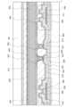
薄膜トランジスタ142は、基板100上に設けた、第2のボトムゲート電極211と、
ゲート絶縁膜102と、第3の酸化物半導体層213cと第4の酸化物半導体領域213
dからなる酸化物半導体層213と、第2のチャネル保護層216と、ソース電極および
ドレイン電極(214a、214b)を有する。更には、第2のチャネル保護層216に
接してこれらを覆う第1の保護絶縁膜107と第2の保護絶縁膜108が設けられている
。The
The
The semiconductor device includes an
なお、ソース電極およびドレイン電極の下面と接する低抵抗の第4の酸化物半導体領域2
13dは自己整合的に形成されている。また、本実施の形態にて説明する薄膜トランジス
タ142は、チャネルストップ型の一態様である。なお、第2の保護絶縁膜108上に薄
膜トランジスタ142と重畳する画素電極128が設けられている。The fourth
The
ただし、液晶表示装置は、液晶の劣化を防ぐため、交流駆動が行われている。この交流駆
動により、一定の期間毎に画素電極層に印加する信号電位の極性が正極性或いは負極性に
反転する。画素電極層に接続するTFTは、一対の電極が交互にソース電極とドレイン電
極の役割を果たす。本明細書では、便宜上、画素の薄膜トランジスタの電極のうち、一方
をソース電極と呼び、もう一方をドレイン電極と呼ぶが、実際には、交流駆動の際に一方
の電極が交互にソース電極とドレイン電極として機能する。また、リーク電流の低減を図
るため、画素に配置する薄膜トランジスタ142の第2のボトムゲート電極の幅を駆動回
路の薄膜トランジスタ141の第1のボトムゲート電極の幅よりも狭くしてもよい。また
、リーク電流の低減を図るため、画素に配置する薄膜トランジスタ142のボトムゲート
電極がソース電極またはドレイン電極と重ならないように設計してもよい。However, the liquid crystal display device is AC driven to prevent deterioration of the liquid crystal. This AC driving inverts the polarity of the signal potential applied to the pixel electrode layer to positive or negative at regular intervals. In the TFT connected to the pixel electrode layer, a pair of electrodes alternately serves as a source electrode and a drain electrode. In this specification, for convenience, one of the electrodes of the thin film transistor of the pixel is called a source electrode and the other is called a drain electrode, but in reality, one electrode alternately functions as a source electrode and a drain electrode during AC driving. In addition, in order to reduce leakage current, the width of the second bottom gate electrode of the
また、画素に配置される薄膜トランジスタ142はシングルゲート構造の薄膜トランジス
タを用いて説明したが、必要に応じて、チャネル形成領域を複数有するマルチゲート構造
の薄膜トランジスタも形成することができる。Although the
また、薄膜トランジスタ142には、可視光を透過する第3の酸化物半導体層213cと
、可視光を透過する導電膜を用いた第2のボトムゲート電極211及びソース電極および
ドレイン電極(214a、214b)と、可視光を透過する基板100と、可視光を透過
する第2のチャネル保護層216と、第1の保護絶縁膜107と、第2の保護絶縁膜10
8を用いている。従って、薄膜トランジスタ142は可視光を透過するいわゆる透明トラ
ンジスタである。The
Therefore, the
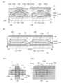
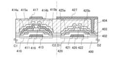
図2及び図3に薄膜トランジスタ141及び142の作製工程の断面図を示す。Figures 2 and 3 show cross-sectional views of the manufacturing process of
基板100は、可視光を透過し絶縁表面を有する。具体的には、アルミノシリケートガラ
ス、アルミノホウケイ酸ガラス、バリウムホウケイ酸ガラスのような電子工業用に使われ
るガラス基板(「無アルカリガラス基板」とも呼ばれる)、本作製工程の処理温度に耐え
うる耐熱性を有するプラスチック基板などを用いることができる。絶縁表面を有する基板
100がマザーガラスの場合、第1世代(320mm×400mm)、第2世代(400
mm×500mm)、第3世代(550mm×650mm)、第4世代(680mm×8
80mm、または730mm×920mm)、第5世代(1000mm×1200mmま
たは1100mm×1250mm)、第6世代1500mm×1800mm)、第7世代
(1900mm×2200mm)、第8世代(2160mm×2460mm)、第9世代
(2400mm×2800mm、2450mm×3050mm)、第10世代(2950
mm×3400mm)などの大きさのものを用いることができる。The
mm x 500 mm), 3rd generation (550 mm x 650 mm), 4th generation (680 mm x 8
80mm, or 730mm x 920mm), 5th generation (1000mm x 1200mm or 1100mm x 1250mm), 6th generation 1500mm x 1800mm), 7th generation (1900mm x 2200mm), 8th generation (2160mm x 2460mm), 9th generation (2400mm x 2800mm, 2450mm x 3050mm), 10th generation (2950
For example, a size of 300 mm×3,400 mm can be used.
また、下地絶縁層を基板100と第1のボトムゲート電極111の間、及び基板100と
第2のボトムゲート電極211の間に設けてもよい。下地絶縁層は、基板100から不純
物元素(例えばナトリウムなど)が薄膜トランジスタへ拡散する現象を防止する絶縁膜に
より形成すればよく、例えば窒化シリコン、酸化シリコン、窒化酸化シリコン、または酸
化窒化シリコンから選ばれた一または複数の膜により積層して形成することができる。Further, a base insulating layer may be provided between the
絶縁表面を有する基板100上に第1のボトムゲート電極111及び第2のボトムゲート
電極211を設ける。第1のボトムゲート電極111及び第2のボトムゲート電極211
は可視光を透過する導電膜を用いて形成する。A first
is formed using a conductive film that transmits visible light.
第1のボトムゲート電極111及び第2のボトムゲート電極211は、透光性を有する導
電性材料、例えば、酸化タングステンを含むインジウム酸化物、酸化タングステンを含む
インジウム亜鉛酸化物、酸化チタンを含むインジウム酸化物、酸化チタンを含むインジウ
ム錫酸化物、インジウム錫酸化物(以下、ITOと示す。)、インジウム亜鉛酸化物、酸
化ケイ素を添加したインジウム錫酸化物、In-Sn-Zn-O系、In-Al-Zn-
O系、Sn-Ga-Zn-O系、Al-Ga-Zn-O系、Sn-Al-Zn-O系、S
n-Zn-O系、Al-Zn-O系、In-O系、Sn-O系、Zn-Oなどの透光性を
有する導電性材料を用い、膜厚は50nm以上300nm以下の範囲内で適宜選択して形
成する。The first
O-based, Sn-Ga-Zn-O-based, Al-Ga-Zn-O-based, Sn-Al-Zn-O-based, S
The insulating film is formed using a light-transmitting conductive material such as n-Zn-O, Al-Zn-O, In-O, Sn-O, or Zn-O, with a thickness appropriately selected within the range of 50 nm to 300 nm.
また、例えば、窒素ガスを含む雰囲気中でスパッタ法によりIn(インジウム)、Ga(
ガリウム)、およびZn(亜鉛)を含む酸化物半導体ターゲット(In2O3:Ga2O
3:ZnO=1:1:1(モル数比))を用いて得たインジウム、ガリウム、および亜鉛
を含む酸窒化物膜や、Al-Zn-O系非単結晶膜や、窒素を含ませたAl-Zn-O系
非単結晶膜、即ちAl-Zn-O-N系非単結晶膜(AZON膜とも呼ぶ)を用いてもよ
い。In addition, for example, In (indium), Ga (
gallium), and an oxide semiconductor target containing Zn (zinc) (In2 O3 :Ga2 O
Alternatively , an oxynitride film containing indium, gallium, and zinc obtained using Al—Zn—O (Al—Zn—O=1:1:1 (molar ratio)), an Al—Zn—O based non-single crystal film, or an Al—Zn—O based non-single crystal film containing nitrogen, that is, an Al—Zn—O—N based non-single crystal film (also called an AZON film) may be used.
透光性を有する導電膜の成膜方法は、スパッタ法や真空蒸着法(電子ビーム蒸着法など)
や、アーク放電イオンプレーティング法や、スプレー法を用いる。また、スパッタ法を用
いる場合、SiO2を2重量%以上10重量%以下含むターゲットを用いて成膜を行い、
透光性を有する導電膜に結晶化を阻害するSiOx(X>0)を含ませ、後の工程で行う
脱水化または脱水素化のための加熱処理の際に結晶化してしまうのを抑制することが好ま
しい。The method for forming a conductive film having light-transmitting properties is a sputtering method or a vacuum deposition method (such as an electron beam deposition method).
In the case of using the sputtering method, the film is formed using a target containing 2% by weight or more and 10% by weight or less ofSiO2 ,
It is preferable that the light-transmitting conductive film contains SiOx (X>0) which inhibits crystallization, thereby suppressing crystallization during heat treatment for dehydration or dehydrogenation performed in a later step.
第1のボトムゲート電極111を含む配線層は、第2のボトムゲート電極211と同じく
、可視光を透過する導電性材料を用いて形成してもよいが、モリブデン、タングステンな
どの耐熱性を有する金属材料またはこれらを主成分とする合金材料を用いて、単層でまた
は積層して形成してもよい。The wiring layer including the first
第1のボトムゲート電極111を含む配線層を第2のボトムゲート電極211と同じ導電
膜を用いて形成すれば、工程数を削減できるため好ましい。また、第1のボトムゲート電
極111を含む配線層を、耐熱性を有する金属材料またはこれらを主成分とする合金材料
を用いて形成すれば、配線抵抗を低減できるため好ましい。It is preferable to form the wiring layer including the first
例えば、第1のボトムゲート電極111を含む配線層を2層の積層構造とする場合には、
アルミニウム層上にモリブデン層が積層された2層構造、または銅層上にモリブデン層を
積層した2層構造、または銅層上に窒化チタン層若しくは窒化タンタルを積層した2層構
造、窒化チタン層とモリブデン層とを積層した2層構造とすることが好ましい。3層の積
層構造とする場合には、タングステン層または窒化タングステンと、アルミニウムとシリ
コンの合金またはアルミニウムとチタンの合金と、窒化チタンまたはチタン層と、を積層
した3層構造とすることが好ましい。For example, when the wiring layer including the first
A two-layer structure in which a molybdenum layer is laminated on an aluminum layer, or a two-layer structure in which a molybdenum layer is laminated on a copper layer, or a two-layer structure in which a titanium nitride layer or a tantalum nitride layer is laminated on a copper layer, or a two-layer structure in which a titanium nitride layer and a molybdenum layer are laminated, is preferable. In the case of a three-layer laminate structure, a three-layer structure in which a tungsten layer or a tungsten nitride layer, an alloy of aluminum and silicon or an alloy of aluminum and titanium, and a titanium nitride or a titanium layer are laminated is preferable.
本実施の形態では、可視光を透過する導電膜を基板100の全面に形成した後、第1のフ
ォトリソグラフィ工程を行い、該導電膜上にレジストマスクを形成し、エッチングにより
不要な部分を除去することで配線および電極(第1のボトムゲート電極111及び第2の
ボトムゲート電極211を含むゲート配線、容量配線、および端子電極など)を形成する
。In this embodiment, after a conductive film that transmits visible light is formed over the entire surface of the
次いで、第1のボトムゲート電極111及び第2のボトムゲート電極211上にゲート絶
縁膜102を形成する。本実施の形態では窒化シリコンを単層でゲート絶縁膜102を形
成する。Next, the
ゲート絶縁膜102は、酸化シリコン、窒化シリコン、酸化窒化シリコンまたは窒化酸化
シリコンを単層でまたは積層して形成することができる。ここでは、窒化シリコン膜を単
層で用いた。The
ゲート絶縁膜102の成膜方法としては、例えば、プラズマCVD法またはスパッタリン
グ法などを用いることができる。プラズマCVD法を用いる場合は、原料ガスとして、S
iH4と、酸素および窒素のいずれか一方または双方と、を用いてプラズマCVD法によ
り酸化窒化シリコン層を形成すればよい。または、酸素と窒素に代えて、一酸化二窒素な
どを用いてもよい。The
A silicon oxynitride layer may be formed by plasma CVD usingiH4 and either or both of oxygen and nitrogen. Alternatively, dinitrogen monoxide or the like may be used instead of oxygen and nitrogen.
次いで、ゲート絶縁膜102上に、酸化物半導体膜を形成する。Then, an oxide semiconductor film is formed on the
酸化物半導体膜は、In-Ga-Zn-O系非単結晶膜、In-Sn-Zn-O系、In
-Al-Zn-O系、Sn-Ga-Zn-O系、Al-Ga-Zn-O系、Sn-Al-
Zn-O系、In-Zn-O系、Sn-Zn-O系、Al-Zn-O系、In-O系、S
n-O系、Zn-O系の酸化物半導体膜を用いる。本実施の形態では、In-Ga-Zn
-O系酸化物半導体ターゲットを用いてスパッタ法により成膜する。また、酸化物半導体
膜は、希ガス(代表的にはアルゴン)雰囲気下、酸素雰囲気下、又は希ガス(代表的には
アルゴン)及び酸素雰囲気下においてスパッタ法により形成することができる。また、ス
パッタ法を用いる場合、SiO2を2重量%以上10重量%以下含むターゲットを用いて
成膜を行い、酸化物半導体膜に結晶化を阻害するSiOx(X>0)を含ませ、後の工程
で行う脱水化または脱水素化のための加熱処理の際に結晶化してしまうのを抑制すること
が好ましい。The oxide semiconductor film may be an In-Ga-Zn-O based non-single crystal film, an In-Sn-Zn-O based film, or an In
-Al-Zn-O system, Sn-Ga-Zn-O system, Al-Ga-Zn-O system, Sn-Al-
Zn-O series, In-Zn-O series, Sn-Zn-O series, Al-Zn-O series, In-O series, S
In this embodiment, an In—Ga—Zn oxide semiconductor film is used.
The oxide semiconductor film is formed by a sputtering method using a -O-based oxide semiconductor target. The oxide semiconductor film can be formed by a sputtering method in a rare gas (typically argon) atmosphere, an oxygen atmosphere, or a rare gas (typically argon) and oxygen atmosphere. When a sputtering method is used, the film is formed using a target containing 2 wt % to 10 wt % of SiO2 , and the oxide semiconductor film is made to contain SiOx (X>0) that inhibits crystallization, thereby suppressing crystallization during heat treatment for dehydration or dehydrogenation performed in a later step.
次いで、酸化物半導体膜を第2のフォトリソグラフィ工程により島状の第1の酸化物半導
体層113a及び213aに加工する(図2(A)を参照)。また、島状の酸化物半導体
層を形成するためのレジストマスクをインクジェット法で形成してもよい。レジストマス
クをインクジェット法で形成するとフォトマスクを使用しないため、製造コストを低減で
きる。Next, the oxide semiconductor film is processed into island-shaped first
なお、酸化物半導体膜をスパッタ法により形成する前に、アルゴンガスを導入してプラズ
マを発生させて逆スパッタを行い、ゲート絶縁膜102の表面に付着しているゴミなどを
除去することが好ましい。Note that before the oxide semiconductor film is formed by a sputtering method, dust and the like attached to the surface of the
逆スパッタとは、ターゲット側に電圧を印加せずに、アルゴン雰囲気下で基板側にRF電
源を用いて電圧を印加して基板近傍にプラズマを形成して表面を改質する方法である。な
お、アルゴン雰囲気に代えて窒素、ヘリウム、酸素などを用いてもよい。Reverse sputtering is a method of modifying the surface by applying a voltage to the substrate side using an RF power source in an argon atmosphere without applying a voltage to the target side. Note that nitrogen, helium, oxygen, etc. may be used instead of the argon atmosphere.
次いで、第1の酸化物半導体層113a及び213aに対して、脱水化または脱水素化を
行う。脱水化または脱水素化を行う第1の加熱処理の温度は、350℃以上基板の歪み点
未満、好ましくは400℃以上とする。ここでは、加熱処理装置の一つである電気炉に基
板を導入し、酸化物半導体層に対して窒素雰囲気下において加熱処理を行った後、酸化物
半導体層を大気に触れさせることなく冷却することで、酸化物半導体層への水や水素の再
混入を防ぐ。このようにして、第2の酸化物半導体層113b及び213bを得る(図2
(B)を参照)。Next, the first
(See (B)).
本実施の形態では、酸化物半導体層の脱水化または脱水素化を行う加熱温度Tから、再び
水が入らないような十分な温度まで同じ炉を用い、具体的には加熱温度Tよりも100℃
以上下がるまで窒素雰囲気下で徐冷する。また、窒素雰囲気に限定されず、ヘリウム、ネ
オン、アルゴン等の不活性ガス雰囲気下或いは減圧下において脱水化または脱水素化を行
う。In this embodiment, the same furnace is used from the heating temperature T at which the oxide semiconductor layer is dehydrated or dehydrogenated to a temperature at which water does not enter again.
The dehydration or dehydrogenation is carried out in an inert gas atmosphere, such as helium, neon, or argon, or under reduced pressure, without being limited to a nitrogen atmosphere.
なお、第1の加熱処理においては、窒素、またはヘリウム、ネオン、アルゴン等の希ガス
に、水、水素などが含まれないことが好ましい。または、加熱処理装置に導入する窒素、
またはヘリウム、ネオン、アルゴン等の希ガスの純度を、6N(99.9999%)以上
、好ましくは7N(99.99999%)以上、(即ち不純物濃度を1ppm以下、好ま
しくは0.1ppm以下)とすることが好ましい。In the first heat treatment, it is preferable that nitrogen or a rare gas such as helium, neon, or argon does not contain water, hydrogen, or the like.
Alternatively, it is preferable that the purity of rare gas such as helium, neon, or argon is 6N (99.9999%) or more, preferably 7N (99.99999%) or more (i.e., impurity concentration is 1 ppm or less, preferably 0.1 ppm or less).
また、第1の加熱処理の条件、または酸化物半導体層の材料によっては、結晶化し、微結
晶膜または多結晶膜となる場合もある。Depending on the conditions of the first heat treatment or the material of the oxide semiconductor layer, the oxide semiconductor layer might be crystallized and become a microcrystalline film or a polycrystalline film.
また、酸化物半導体層の第1の加熱処理は、島状の酸化物半導体層に加工する前の酸化物
半導体膜に行うこともできる。その場合には、第1の加熱処理後に、加熱装置から基板を
取り出し、第2のフォトリソグラフィ工程を行う。The first heat treatment of the oxide semiconductor layer can be performed on the oxide semiconductor film before it is processed into an island-shaped oxide semiconductor layer. In that case, after the first heat treatment, the substrate is taken out of the heating apparatus and a second photolithography step is performed.
また、酸化物半導体膜の成膜前に、不活性ガス雰囲気(窒素、またはヘリウム、ネオン、
アルゴン等)下、酸素雰囲気、或いは減圧下において加熱処理(400℃以上基板の歪み
点未満)を行い、ゲート絶縁層内に含まれる水素及び水などの不純物を除去してもよい。In addition, before the formation of the oxide semiconductor film, an inert gas atmosphere (nitrogen, helium, neon,
Heat treatment (400° C. or higher and lower than the distortion point of the substrate) may be performed in an atmosphere of argon, oxygen, or reduced pressure to remove impurities such as hydrogen and water contained in the gate insulating layer.
次いで、第2の酸化物半導体層113b及び213bと接して、チャネル保護層となる絶
縁膜を形成する。第2の酸化物半導体層113b及び213bに接して形成するチャネル
保護層となる絶縁膜は、酸化物絶縁膜からなり、少なくとも1nm以上の膜厚とすること
ができる。さらに、当該酸化物絶縁膜は、スパッタリング法など、酸化物絶縁膜に水、水
素等の不純物を混入させない方法を適宜用いて形成することができる。Next, an insulating film to be a channel protective layer is formed in contact with the second oxide semiconductor layers 113b and 213b. The insulating film to be a channel protective layer formed in contact with the second oxide semiconductor layers 113b and 213b is made of an oxide insulating film and can have a thickness of at least 1 nm. Furthermore, the oxide insulating film can be formed by appropriately using a method that does not allow impurities such as water and hydrogen to be mixed into the oxide insulating film, such as a sputtering method.
本実施の形態では、酸化物絶縁膜として膜厚300nmの酸化珪素膜をスパッタリング法
を用いて成膜する。成膜時の基板温度は、室温以上300℃以下とすればよく、本実施の
形態では100℃とする。酸化珪素膜のスパッタリング法による成膜は、希ガス(代表的
にはアルゴン)雰囲気下、酸素雰囲気下、または希ガス(代表的にはアルゴン)及び酸素
雰囲気下において行うことができる。また、ターゲットとして酸化珪素ターゲットまたは
珪素ターゲットを用いることができる。例えば、珪素ターゲットを用いて、酸素、及び窒
素雰囲気下でスパッタリング法により酸化珪素を形成することができる。低抵抗化した酸
化物半導体層に接して形成するチャネル保護層は、水分や、水素イオンや、OH-などの
不純物を含まず、これらが外部から侵入することをブロックする無機絶縁膜を用い、代表
的には酸化珪素膜、窒化酸化珪素膜、酸化アルミニウム膜、または酸化窒化アルミニウム
膜などを用いる。In this embodiment, a silicon oxide film having a thickness of 300 nm is formed as the oxide insulating film by a sputtering method. The substrate temperature during film formation may be from room temperature to 300° C., and is set to 100° C. in this embodiment. The silicon oxide film can be formed by sputtering in a rare gas (typically argon) atmosphere, an oxygen atmosphere, or a rare gas (typically argon) and oxygen atmosphere. A silicon oxide target or a silicon target can be used as a target. For example, silicon oxide can be formed by sputtering in an oxygen and nitrogen atmosphere using a silicon target. A channel protective layer formed in contact with the low-resistance oxide semiconductor layer is an inorganic insulating film that does not contain impurities such as moisture, hydrogen ions, and OH− and that blocks the intrusion of these impurities from the outside, and is typically a silicon oxide film, a silicon nitride oxide film, an aluminum oxide film, an aluminum oxynitride film, or the like.
次いで、第3のフォトリソグラフィ工程を行い、チャネル保護層となる絶縁膜上にレジス
トマスクを形成し、エッチングにより不要な部分を除去して第1のチャネル保護層116
及び第2のチャネル保護層216を形成する。Next, a third photolithography process is performed, a resist mask is formed on the insulating film that will become the channel protective layer, and unnecessary portions are removed by etching to form the first channel
And the second
次いで、不活性ガス雰囲気下で第2の加熱処理(好ましくは200℃以上400℃以下、
例えば250℃以上350℃以下)を行う(図2(C)参照。)。例えば、窒素雰囲気下
で250℃、1時間の第2の加熱処理を行う。第2の加熱処理を行うと、第2の酸化物半
導体層113bの一部が第1のチャネル保護層116に接した状態で加熱され、第2の酸
化物半導体層213bの一部が第2のチャネル保護層216に接した状態で加熱される。
また、第2の酸化物半導体層113bの第1のチャネル保護層116が接していない領域
と、第2の酸化物半導体層213bの第1のチャネル保護層216が接していない領域は
、不活性ガス雰囲気に曝された状態で加熱される。Next, a second heat treatment is performed in an inert gas atmosphere (preferably at 200° C. or higher and 400° C. or lower,
For example, a second heat treatment is performed at 250° C. or higher and 350° C. or lower in a nitrogen atmosphere for one hour. By the second heat treatment, part of the second
In addition, a region of the second
以上の工程を経ることによって、成膜後の酸化物半導体膜に対して脱水化または脱水素化
のための加熱処理を行って低抵抗化した後、酸化物半導体膜の一部と接するチャネル保護
層を、酸化物絶縁膜を用いて形成し、チャネル保護層と重なる領域を選択的に酸素過剰な
状態とする。その結果、チャネル保護層と重なるチャネル形成領域は、I型となる。本明
細書では、このI型の酸化物半導体を第3の酸化物半導体と呼ぶ。従って、第1のチャネ
ル保護層116に接した状態で第2の加熱処理された第2の酸化物半導体層113bは第
3の酸化物半導体層113cとなり、第2のチャネル保護層216に接した状態で第2の
加熱処理された第2の酸化物半導体層213bは第3の酸化物半導体層213cとなる。By going through the above steps, the oxide semiconductor film after deposition is subjected to heat treatment for dehydration or dehydrogenation to reduce resistance, and then a channel protective layer in contact with part of the oxide semiconductor film is formed using an oxide insulating film, and a region overlapping with the channel protective layer is selectively made into an oxygen-excess state. As a result, the channel formation region overlapping with the channel protective layer becomes an I-type. In this specification, this I-type oxide semiconductor is called a third oxide semiconductor. Therefore, the second
一方、第2の酸化物半導体層113bの第1のチャネル保護層116が接していない領域
と、第2の酸化物半導体層213bの第1のチャネル保護層216が接していない領域に
は、自己整合的に高抵抗ドレイン領域が形成される。本明細書では、この高抵抗ドレイン
領域を第4の酸化物半導体領域と呼ぶ。従って、第1のチャネル保護層116に接してい
ない第2の酸化物半導体層113bは第4の酸化物半導体領域113dになり、第2のチ
ャネル保護層216に接していない第2の酸化物半導体層213bは第4の酸化物半導体
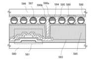
領域213dになる。On the other hand, a high-resistance drain region is formed in a self-aligned manner in a region of the second
次いで、ゲート絶縁膜102、第4の酸化物半導体領域113d及び213d上に可視光
を透過する導電膜を形成する。Next, a conductive film that transmits visible light is formed over the
透光性を有する導電膜の成膜方法は、スパッタ法や真空蒸着法(電子ビーム蒸着法など)
や、アーク放電イオンプレーティング法や、スプレー法を用いる。導電膜の材料としては
、可視光に対して透光性を有する導電材料、例えばIn-Sn-Zn-O系、In-Al
-Zn-O系、Sn-Ga-Zn-O系、Al-Ga-Zn-O系、Sn-Al-Zn-
O系、In-Zn-O系、Sn-Zn-O系、Al-Zn-O系、In-O系、Sn-O
系、Zn-O系の金属酸化物を適用することができ、膜厚は50nm以上300nm以下
の範囲内で適宜選択する。また、スパッタ法を用いる場合、SiO2を2重量%以上10
重量%以下含むターゲットを用いて成膜を行い、透光性を有する導電膜に結晶化を阻害す
るSiOx(X>0)を含ませ、後の工程で行う加熱処理の際に結晶化してしまうのを抑
制することが好ましい。The method for forming a conductive film having light-transmitting properties is a sputtering method or a vacuum deposition method (such as an electron beam deposition method).
The conductive film is made of a conductive material having transparency to visible light, such as In--Sn--Zn--O, In--Al
-Zn-O system, Sn-Ga-Zn-O system, Al-Ga-Zn-O system, Sn-Al-Zn-
O series, In-Zn-O series, Sn-Zn-O series, Al-Zn-O series, In-O series, Sn-O
Metal oxides such as Zn--O and Zn--O can be used, and the film thickness is appropriately selected within the range of 50nm to 300 nm.
It is preferable to form a film using a target containing SiOx (X>0) which inhibits crystallization in a light-transmitting conductive film, thereby suppressing crystallization during a heat treatment performed in a later step.
次に、可視光を透過する導電膜上に金属導電膜を形成する。金属導電膜としては、Al、
Cr、Cu、Ta、Ti、Mo、Wから選ばれた元素、または上述した元素を成分とする
合金か、上述した元素を組み合わせた合金等がある。また、チタン層上にアルミニウム層
と、該アルミニウム層上にチタン層が積層された三層の積層構造、またはモリブデン層上
にアルミニウム層と、該アルミニウム層上にモリブデン層を積層した三層の積層構造とす
ることが好ましい。勿論、金属導電膜として単層、または2層構造、または4層以上の積
層構造としてもよい。Next, a metal conductive film is formed on the conductive film that transmits visible light.
The metal conductive film may be an element selected from Cr, Cu, Ta, Ti, Mo, and W, an alloy containing the above elements, or an alloy combining the above elements. Also, it is preferable to use a three-layered structure in which an aluminum layer is laminated on a titanium layer and a titanium layer is laminated on the aluminum layer, or a three-layered structure in which an aluminum layer is laminated on a molybdenum layer and a molybdenum layer is laminated on the aluminum layer. Of course, the metal conductive film may be a single layer, a two-layered structure, or a four-layered or more laminated structure.
次に、第4のフォトリソグラフィ工程によりレジストマスク134を形成し、選択的にエ
ッチングを行って可視光を透過する導電膜と、金属導電膜の不要な部分をエッチングして
除去し、可視光を透過する導電膜と金属導電膜を積層した電極層を形成する(図3(A)
参照)。Next, a resist
reference).
なお、このエッチングにおいて、第1のチャネル保護層116及び第2のチャネル保護層
216は第3の酸化物半導体層113c及び213cのエッチングストッパーとして機能
するため、第3の酸化物半導体層113c及び213cはエッチングされない。In this etching, since the first
第3の酸化物半導体層113cのチャネル形成領域上に第1のチャネル保護層116を設
け、第3の酸化物半導体層213cのチャネル形成領域上に第2のチャネル保護層216
を設ける構造であるため、第3の酸化物半導体層113c及び213cのチャネル形成領
域を工程時におけるダメージ(エッチング時のプラズマやエッチング剤による膜減りや、
酸化など)から保護できる。従って、薄膜トランジスタ141及び142の信頼性を向上
させることができる。A first channel
Since the third oxide semiconductor layers 113c and 213c have a structure in which the third oxide semiconductor layers 113c and 213c are provided, the channel formation regions of the third oxide semiconductor layers 113c and 213c are prevented from being damaged during etching (such as film reduction due to plasma or an etchant during etching,
Therefore, the reliability of the
また、レジストマスクをインクジェット法で形成してもよい。レジストマスクをインクジ
ェット法で形成するとフォトマスクを使用しないため、製造コストを低減できる。The resist mask may be formed by an ink-jet method, which does not require a photomask and therefore reduces manufacturing costs.
次いで、レジストマスク134を除去した後、第5のフォトリソグラフィ工程を行い、ソ
ース電極及びドレイン電極(115a及び115b)を含む配線層と、薄膜トランジスタ
141を覆うレジストマスク135を形成する。次に、レジストマスク135を用い、エ
ッチングにより不要な導電層(215a、215b)を除去して、透光性を有するソース
電極及びドレイン電極(214a及び214b)を形成する。この段階で薄膜トランジス
タ141及び142が形成される(図3(B)を参照)。Next, after removing the resist
なお、ドレイン電極層、またはソース電極層と重畳した酸化物半導体層に、高抵抗ドレイ
ン領域である第4の酸化物半導体領域が形成されることにより、駆動回路を形成した際の
信頼性の向上を図ることができる。具体的には、ドレイン電極層から第4の酸化物半導体
領域、チャネル形成領域にかけて、導電性を段階的に変化させうるような構造とすること
ができる。そのため、ドレイン電極層に高電源電位VDDを供給する配線に接続して動作
させる場合、ゲート電極層とドレイン電極層との間に高電界が印加されても高抵抗ドレイ
ン領域である第4の酸化物半導体領域がバッファとなり局所的な高電界が印加されず、ト
ランジスタの耐圧を向上させた構成とすることができる。また、ドレイン電極層と重畳し
た酸化物半導体層において、高抵抗ドレイン領域である第4の酸化物半導体領域が形成さ
れることにより、駆動回路を形成した際のチャネル形成領域でのリーク電流の低減を図る
ことができる。Note that by forming a fourth oxide semiconductor region as a high-resistance drain region in the oxide semiconductor layer overlapping with the drain electrode layer or the source electrode layer, reliability can be improved when a driver circuit is formed. Specifically, a structure in which conductivity can be changed stepwise from the drain electrode layer to the fourth oxide semiconductor region and the channel formation region can be provided. Therefore, when the drain electrode layer is connected to a wiring that supplies a high power supply potential VDD and is operated, even if a high electric field is applied between the gate electrode layer and the drain electrode layer, the fourth oxide semiconductor region as a high-resistance drain region serves as a buffer to prevent a local high electric field from being applied, and a withstand voltage of the transistor can be improved. Furthermore, by forming the fourth oxide semiconductor region as a high-resistance drain region in the oxide semiconductor layer overlapping with the drain electrode layer, leakage current in a channel formation region can be reduced when a driver circuit is formed.
具体的には、薄膜トランジスタ141においては、配線抵抗が低い金属導電膜で形成した
ドレイン電極である導電層115bが、透光性を有する導電層114bと、高抵抗ドレイ
ン領域である第4の酸化物半導体領域113dを経て、チャネル形成領域である第3の酸
化物半導体層113cに電気的に接続されている。従って、透光性を有する導電層114
bは低抵抗ドレイン領域(LRN領域とも呼ぶ)ということができる。また、薄膜トラン
ジスタ142においては、透光性を有する導電膜と、高抵抗ドレイン領域である第4の酸
化物半導体領域213dを経て、チャネル形成領域である第3の酸化物半導体層213c
に接続されている。Specifically, in the
In the
is connected to
次いで、レジストマスク135を除去し、第1のチャネル保護層116及び第2のチャネ
ル保護層216上に第1の保護絶縁膜107を形成する。第1の保護絶縁膜107は、膜
中の水分、水素イオン、およびOH-などが低減されており、これらの外部からの侵入を
ブロックする。絶縁性無機材料を用いて形成する。具体的には、酸化シリコン、酸化窒化
シリコンまたは窒化酸化シリコン、窒化シリコン、酸化アルミニウム、窒化アルミニウム
等を単層でまたは積層して形成することができる。Next, the resist
ここでは、まず窒化シリコン膜を用いて、ゲート絶縁膜102に接する第1の保護絶縁膜
107aを形成する。窒化シリコン膜を用いて、ゲート絶縁膜102と第1の保護絶縁膜
107aを形成することで、薄膜トランジスタ141及び142の周囲を囲んで、同じ無
機絶縁膜同士が接する構造にでき、薄膜トランジスタの封止状態をより良好な状態にでき
る。窒化シリコン上に組成の異なる保護絶縁膜、例えば酸化窒化シリコンを積層して第1
の保護絶縁膜107としてもよい。Here, a silicon nitride film is first used to form the first protective insulating
The protective
第1の保護絶縁膜107の他の構成としては、例えば、スパッタ法を用いて厚さ300n
mの酸化シリコン膜を形成し、さらに窒化シリコンを積層してもよい。形成時の基板温度
は、室温以上300℃以下とすればよく、本実施の形態では100℃とする。酸化シリコ
ン膜のスパッタ法による形成は、希ガス(代表的にはアルゴン)雰囲気下、酸素雰囲気下
、または希ガス(代表的にはアルゴン)と酸素の混合ガス雰囲気下において行うことがで
きる。また、ターゲットとして酸化シリコンターゲットを用いてもシリコンターゲットを
用いてもよい。例えばシリコンターゲットを用いて、酸素を含む雰囲気下でスパッタ法に
より酸化シリコンを形成することができる。As another configuration of the first protective insulating
A silicon oxide film having a thickness of 100 nm may be formed, and silicon nitride may be further stacked on the silicon oxide film. The substrate temperature during the formation may be from room temperature to 300° C., and is set to 100° C. in this embodiment. The silicon oxide film may be formed by sputtering in a rare gas (typically argon) atmosphere, an oxygen atmosphere, or a mixed gas atmosphere of a rare gas (typically argon) and oxygen. In addition, either a silicon oxide target or a silicon target may be used as the target. For example, silicon oxide can be formed by sputtering in an atmosphere containing oxygen using a silicon target.
次に、薄膜トランジスタ141及び142を覆う第2の保護絶縁膜108を第1の保護絶
縁膜107上に形成する。Next, the second protective insulating
第2の保護絶縁膜108は、第1の保護絶縁膜107を介して、第1のチャネル保護層1
16及び第2のチャネル保護層216と、ソース電極及びドレイン電極(115a、11
5b、214a、214b)を覆う。The second protective insulating
16 and the second
5b, 214a, 214b).
第2の保護絶縁膜108は、例えば、0.5μm~3μmの厚さを有する感光性または非
感光性の有機材料を用いることができる。第2の保護絶縁膜108に用いることができる
感光性または非感光性の有機材料としては、ポリイミド、アクリル、ポリアミド、ポリイ
ミドアミド、レジスト若しくはベンゾシクロブテン、またはこれらを積層して形成したも
のなどを挙げることができる。また上記有機材料の他に、低誘電率材料(low-k材料
)、シロキサン系樹脂、PSG(リンガラス)、BPSG(リンボロンガラス)等を用い
ることができる。また、これらの材料で形成される絶縁膜を複数積層させることで、第2
の保護絶縁膜108を形成してもよい。The second protective insulating
A protective
なおシロキサン系樹脂とは、シロキサン系材料を出発材料として形成されたSi-O-S
i結合を含む樹脂に相当する。シロキサン系樹脂は置換基としては有機基(例えばアルキ
ル基やアリール基)やフルオロ基を用いても良い。また、有機基はフルオロ基を有してい
ても良い。The siloxane-based resin is a Si—O—S resin formed using a siloxane-based material as a starting material.
The siloxane-based resin corresponds to a resin containing an i bond. The siloxane-based resin may have an organic group (e.g., an alkyl group or an aryl group) or a fluoro group as a substituent. The organic group may have a fluoro group.
第2の保護絶縁膜108の形成法は、特に限定されず、その材料に応じて、スパッタ法、
SOG法、スピンコート、ディップ、スプレー塗布、液滴吐出法(インクジェット法、ス
クリーン印刷、オフセット印刷等)、ドクターナイフ、ロールコーター、カーテンコータ
ー、ナイフコーター等を用いることができる。The method for forming the second protective insulating
An SOG method, spin coating, dipping, spray coating, a droplet discharging method (inkjet method, screen printing, offset printing, etc.), a doctor knife, a roll coater, a curtain coater, a knife coater, etc. can be used.
本実施の形態では、第2の保護絶縁膜108として、感光性のポリイミドを塗布法により
形成する。ポリイミドを全面に塗布した後に、露光、現像および焼成を行って、表面が平
坦な1.5μmの厚さのポリイミドからなる第2の保護絶縁膜108を形成する。In this embodiment, photosensitive polyimide is formed by a coating method as the second protective insulating
第2の保護絶縁膜108を設けることで、薄膜トランジスタ141及び142の構造によ
り生じる凹凸を緩和し、上面を平坦にすることができる。なお、樹脂層に限定されず、上
面が平坦となる方法(スピンコーティング法またはリフロー法など)により形成すること
ができるものであればよい。By providing the second protective insulating
次いで、第1の保護絶縁膜107をエッチングにより開口し、薄膜トランジスタ142の
ドレイン電極214bに達するコンタクトホール125を形成する。Next, the first protective insulating
また、薄膜トランジスタ141において、バックゲート電極129を第1のボトムゲート
電極111と接続する場合は、バックゲート電極129となる導電膜を形成する前に、第
2の保護絶縁膜108、第1の保護絶縁膜107及びゲート絶縁膜102の図示されてい
ない所定の箇所に開口部を設けておく。In addition, in the
次いで、第2の保護絶縁膜108上に可視光を透過する導電膜を形成する。可視光を透過
する導電膜としては、第1のボトムゲート電極111及び第2のボトムゲート電極211
と同様の導電膜を適用することができる。また、バックゲート電極129と画素電極12
8を同じ材料とすることで工程を簡略にできる。Next, a conductive film that transmits visible light is formed over the second protective insulating
In addition, the
By using the same material for 8, the process can be simplified.
次いで、第6のフォトリソグラフィ工程を行い、該導電膜上にレジストマスクを形成し、
エッチングにより不要な部分を除去してバックゲート電極129と画素電極128を含む
配線層を形成する。バックゲート電極129及び画素電極128を含む配線層を選択的に
エッチングして所望の上面形状にする際に、第2の保護絶縁膜108はエッチングストッ
パーとして機能する。Next, a sixth photolithography step is performed to form a resist mask over the conductive film,
Unnecessary portions are removed by etching to form a wiring layer including the
なお、バックゲート電極129は、ソース電極及びドレイン電極間の第3の酸化物半導体
層113cが第1のチャネル保護層116と重なる領域を覆って配置されていれば良く、
バックゲート電極129の幅を短くすれば寄生容量を低減できる。Note that the
By shortening the width of the
また、画素電極128は薄膜トランジスタ142のドレイン電極214bとコンタクトホ
ール125を介して接続する(図3(C)を参照)。In addition, the
また、窒素雰囲気下または大気雰囲気下(大気中)において薄膜トランジスタ141及び
142に加熱処理を行ってもよい。加熱処理は、好ましくは温度350℃以下であって、
第1の保護絶縁膜107となる絶縁膜を形成した後であればいつでもよい。例えば、窒素
雰囲気下で350℃、1時間の加熱処理を行う。該加熱処理を行うと薄膜トランジスタ1
41及び142の電気的特性のばらつきを軽減することができる。Alternatively, the
The heat treatment may be performed at any time after the insulating film that becomes the first protective insulating
This can reduce the variation in the electrical characteristics of 41 and 142.
以上の工程を経ることによって図1(A)に示す薄膜トランジスタ141及び142を形
成することができる。Through the above steps, the
なお、図2(A)及び図2(B)において、チャネル保護層となる絶縁膜を形成する前に
、露出している第2の酸化物半導体層113b及び213bに対して酸素ラジカル処理を
行ってもよい。酸素ラジカル処理を行うことによって、酸化物半導体層の露出面近傍を改
質し、酸素過剰領域とすることができる。酸素ラジカルは、酸素を含むガスを用いてプラ
ズマ発生装置により供給されてもよいし、またはオゾン発生装置により供給されてもよい
。供給された酸素ラジカルまたは酸素を薄膜に照射することによって第2の酸化物半導体
層113b及び213bの表面(バックチャネル部の表面)を改質することができる。ま
た、酸素ラジカル処理に限定されず、アルゴンと酸素のラジカル処理を行ってもよい。ア
ルゴンと酸素のラジカル処理とは、アルゴンガスと酸素ガスを導入してプラズマを発生さ
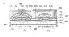
せて薄膜表面の改質を行うことである。2A and 2B, before forming an insulating film to be a channel protective layer, oxygen radical treatment may be performed on the exposed second oxide semiconductor layers 113b and 213b. By performing the oxygen radical treatment, the vicinity of the exposed surface of the oxide semiconductor layer can be modified to become an oxygen excess region. The oxygen radicals may be supplied by a plasma generator using a gas containing oxygen, or may be supplied by an ozone generator. The surfaces (surfaces of the back channel portion) of the second oxide semiconductor layers 113b and 213b can be modified by irradiating the thin film with the supplied oxygen radicals or oxygen. In addition, the treatment is not limited to the oxygen radical treatment, and argon and oxygen radical treatment may be performed. The argon and oxygen radical treatment refers to modifying the thin film surface by introducing argon gas and oxygen gas to generate plasma.
また、窒化シリコン膜上に酸化シリコン膜を形成した2層からなる積層膜をゲート絶縁膜
102に用いた薄膜トランジスタ210及び薄膜トランジスタ220の構成を図7に示す
。酸化物半導体層に接するゲート絶縁膜102bが酸化シリコン膜である場合、チャネル
保護層を酸化シリコン膜から形成する際、ゲート絶縁膜102bがエッチングされ、ゲー
ト絶縁膜102bの島状の酸化物半導体層に重なる領域の膜厚より、ゲート絶縁膜102
bの島状の酸化物半導体層に重ならない領域の膜厚は薄くなる。7 shows the structures of a
The thickness of the region b that does not overlap with the island-shaped oxide semiconductor layer is thin.
薄膜トランジスタ210及び220はゲート絶縁膜102と第1の保護絶縁膜107が互
いに接し、またゲート絶縁膜102と第1の保護絶縁膜107を同じ無機絶縁膜材料を用
いて形成することができる。薄膜トランジスタ210及び220の周囲を囲んで、同じ無
機絶縁膜同士が接する構造とすることで、薄膜トランジスタの封止状態がより良好な状態
にできる。同種の無機絶縁膜同士を接する構造とする場合、上述の無機絶縁膜を用いるこ
とができるが、特に窒化シリコン膜は不純物のバリア性に優れているため好ましい。In the
また、画素電極128を形成するためのレジストマスクをインクジェット法で形成しても
よい。レジストマスクをインクジェット法で形成するとフォトマスクを使用しないため、
製造コストを低減できる。In addition, a resist mask for forming the
Manufacturing costs can be reduced.
以上の工程により、7枚のフォトマスクを用いて、同一基板上に薄膜トランジスタ141
及び薄膜トランジスタ142、もしくは薄膜トランジスタ210及び薄膜トランジスタ2
20を作り分けて形成できる。Through the above steps, the
and
20 can be made and formed separately.
バックゲート電極129を第3の酸化物半導体層113cのチャネル形成領域と重なる位
置に設けることによって、薄膜トランジスタの信頼性を調べるためのバイアス-熱ストレ
ス試験(以下、BT試験という)において、BT試験前後における薄膜トランジスタ14
1のしきい値電圧の変化量を低減することができる。また、バックゲート電極129の電
位は、ボトムゲート電極111と同じでもよいし、異なっていても良い。また、バックゲ
ート電極129の電位がGND、0V、或いはフローティング状態であってもよい。By providing the
It is possible to reduce the amount of change in the threshold voltage of the
本実施の形態の薄膜トランジスタが有するチャネル形成領域の半導体層は高抵抗化領域で
あるので、薄膜トランジスタの電気的特性は安定化し、オフ電流の増加などを防止するこ
とができる。よって、電気的特性が良好で信頼性のよい薄膜トランジスタを有する半導体
装置とすることが可能となる。Since the semiconductor layer of the channel formation region of the thin film transistor of this embodiment is a high resistance region, the electrical characteristics of the thin film transistor are stabilized and an increase in off current can be prevented, etc. Therefore, a semiconductor device including a thin film transistor with good electrical characteristics and high reliability can be obtained.
また、薄膜トランジスタ141及び142、並びに薄膜トランジスタ210及び220に
おいて、ソース電極及びドレイン電極が接するソース領域及びドレイン領域に第4の酸化
物半導体領域が形成されているため、コンタクト抵抗が抑制され、高いオン電流が得られ
る。In addition, in the
なお、本実施の形態は、本明細書で示す他の実施の形態と適宜組み合わせることができる
。Note that this embodiment mode can be appropriately combined with other embodiment modes described in this specification.
(実施の形態2)
本実施の形態は、本発明の一態様であって実施の形態1とは異なる薄膜トランジスタおよ
びその作製方法について説明する。(Embodiment 2)
In this embodiment, a thin film transistor which is one embodiment of the present invention and is different from that in
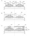
図4(A)に、本発明の一態様である薄膜トランジスタ143及び144の断面図を示す
。薄膜トランジスタ143及び144は同一の基板100上に形成され、どちらもボトム
ゲート型の薄膜トランジスタである。薄膜トランジスタ143は駆動回路に配置され、薄
膜トランジスタ144は画素に配置されている。4A shows a cross-sectional view of
図4(C1)は駆動回路に配置されるチャネルストップ型の薄膜トランジスタ143の平
面図であり、図4(A)は図4(C1)の線C1-C2における断面図である。また、図
4(B)は、図4(C1)の線C3-C4における断面図である。Fig. 4C1 is a plan view of a channel stop type
また、図4(C2)は画素に配置されるチャネルストップ型の薄膜トランジスタ144の
平面図であり、図4(A)は図4(C2)の線D1-D2における断面図である。また、
図4(B)は、図4(C2)の線D3-D4における断面図である。4C2 is a plan view of a channel stop type
FIG. 4B is a cross-sectional view taken along line D3-D4 in FIG.
薄膜トランジスタ143は、基板100上に設けた、第1のボトムゲート電極111と、
ゲート絶縁膜102と、第3の酸化物半導体層113cと、第1のチャネル保護層116
と、ソース電極およびドレイン電極を有する。なお、ソース電極およびドレイン電極は、
第1の導電層114a上に第2の導電層115aを積層した導電層と、第1の導電層11
4b上に第2の導電層115bを積層した導電層を用いて形成されている。更には、第1
のチャネル保護層116に接してこれらを覆う第1の保護絶縁膜107と第2の保護絶縁
膜108と、第2の保護絶縁膜108上に設けられ、第3の酸化物半導体層113cと重
畳するバックゲート電極129が設けられている。また、本実施の形態にて説明する薄膜
トランジスタ143は、チャネルストップ型の一態様である。The
The
and a source electrode and a drain electrode. The source electrode and the drain electrode are
A conductive layer in which a second
The first
A first protective insulating
また、液晶表示装置において、同一基板上に画素部と駆動回路を形成する場合、駆動回路
において、インバータ回路、NAND回路、NOR回路、ラッチ回路といった論理ゲート
を構成する薄膜トランジスタや、センスアンプ、定電圧発生回路、VCOといったアナロ
グ回路を構成する薄膜トランジスタは、ソース電極とドレイン電極間に正極性のみ、もし
くは負極性のみが印加される。従って、第3の酸化物半導体層113cの耐圧が要求され
るソース電極とドレイン電極のいずれか一方の幅をもう一方の幅よりも広く設計してもよ
い。また、第3の酸化物半導体層113cがボトムゲート電極と重なる幅を広くしてもよ
い。In addition, in a liquid crystal display device, when a pixel portion and a driver circuit are formed on the same substrate, thin film transistors constituting logic gates such as inverter circuits, NAND circuits, NOR circuits, and latch circuits in the driver circuit, and thin film transistors constituting analog circuits such as sense amplifiers, constant voltage generating circuits, and VCOs have only positive polarity or only negative polarity applied between the source electrode and the drain electrode. Therefore, the width of either the source electrode or the drain electrode, which requires the withstand voltage of the third
また、駆動回路に配置される薄膜トランジスタ143はシングルゲート構造の薄膜トラン
ジスタを用いて説明したが、必要に応じて、チャネル形成領域を複数有するマルチゲート
構造の薄膜トランジスタも形成することができる。Although the
また、第3の酸化物半導体層113cの上方に重なるバックゲート電極129を設ける。
バックゲート電極129をボトムゲート電極111と電気的に接続し、同電位とすること
で、ボトムゲート電極111とバックゲート電極129の間に配置された第3の酸化物半
導体層113cに上下からゲート電圧を印加することができる。また、ボトムゲート電極
111とバックゲート電極129を異なる電位、例えば固定電位、GND、0Vとする場
合には、TFTの電気特性、例えばしきい値電圧などを制御することができる。なお、本
明細書中では、第3の酸化物半導体層113cの上方に重なって形成される導電層を、そ
の電位にかかわらずバックゲート電極129と呼ぶ。したがって、バックゲート電極12
9はフローティング状態であってもよい。In addition, a
By electrically connecting the
9 may be in a floating state.
また、バックゲート電極129と第3の酸化物半導体層113cの間には第1の保護絶縁
膜107と、第2の保護絶縁膜108とを積層する。In addition, a first protective insulating
薄膜トランジスタ144は、基板100上に設けた、第2のボトムゲート電極211と、
ゲート絶縁膜102と、第3の酸化物半導体層213cと、第2のチャネル保護層216
と、ソース電極およびドレイン電極(214a、214b)を有する。更には、第2のチ
ャネル保護層216に接してこれらを覆う第1の保護絶縁膜107と第2の保護絶縁膜1
08が設けられている。従って、本実施の形態にて説明する薄膜トランジスタ144は、
チャネルストップ型の一態様である。なお、第2の保護絶縁膜108上に薄膜トランジス
タ144と重畳する画素電極128が設けられている。The
The
The semiconductor device further includes a first protective insulating
08 is provided.
This is one embodiment of a channel stop type. Note that a
ただし、液晶表示装置は、液晶の劣化を防ぐため、交流駆動が行われている。この交流駆
動により、一定の期間毎に画素電極層に印加する信号電位の極性が正極性或いは負極性に
反転する。画素電極層に接続するTFTは、一対の電極が交互にソース電極とドレイン電
極の役割を果たす。本明細書では、便宜上、画素の薄膜トランジスタの一方をソース電極
と呼び、もう一方をドレイン電極と呼ぶが、実際には、交流駆動の際に一方の電極が交互
にソース電極とドレイン電極として機能する。また、リーク電流の低減を図るため、画素
に配置する薄膜トランジスタ144の第2のボトムゲート電極の幅を駆動回路の薄膜トラ
ンジスタ143の第1のボトムゲート電極の幅よりも狭くしてもよい。また、リーク電流
の低減を図るため、画素に配置する薄膜トランジスタ144のボトムゲート電極がソース
電極またはドレイン電極と重ならないように設計してもよい。However, the liquid crystal display device is AC driven to prevent deterioration of the liquid crystal. This AC driving inverts the polarity of the signal potential applied to the pixel electrode layer to positive or negative at regular intervals. In the TFT connected to the pixel electrode layer, a pair of electrodes alternately serves as a source electrode and a drain electrode. In this specification, for convenience, one of the thin film transistors of the pixel is called a source electrode and the other is called a drain electrode, but in reality, one electrode alternately functions as a source electrode and a drain electrode during AC driving. In addition, in order to reduce leakage current, the width of the second bottom gate electrode of the
また、画素に配置される薄膜トランジスタ144はシングルゲート構造の薄膜トランジス
タを用いて説明したが、必要に応じて、チャネル形成領域を複数有するマルチゲート構造
の薄膜トランジスタも形成することができる。Although the
また、薄膜トランジスタ144は、可視光を透過する第3の酸化物半導体層213cと、
可視光を透過する導電膜を用いた第2のボトムゲート電極211及びソース電極およびド
レイン電極(214a、214b)と、可視光を透過する基板100と、可視光を透過す
る第2のチャネル保護層216と、第1の保護絶縁膜107と、第2の保護絶縁膜108
を用いている。従って、薄膜トランジスタ144は可視光を透過するいわゆる透明トラン
ジスタである。The
A second
Therefore, the
チャネル形成領域を含む酸化物半導体層の材料としては、半導体特性を有する酸化物材料
を用いればよい。具体的には実施の形態1で例示した酸化物半導体材料を用いることがで
きる。As a material for the oxide semiconductor layer including the channel formation region, an oxide material having semiconductor characteristics may be used, specifically, any of the oxide semiconductor materials exemplified in
なお、本実施の形態の薄膜トランジスタは、第3の酸化物半導体層(113c、213c
)をチャネル形成領域に有する。In addition, in the thin film transistor of this embodiment, the third oxide semiconductor layer (113c, 213c
) in the channel formation region.
図5及び図6に薄膜トランジスタ143及び144の作製工程の断面図を示す。なお、絶
縁表面を有する基板100上に第1のボトムゲート電極111及び第2のボトムゲート電
極211を形成し、第1のボトムゲート電極111及び第2のボトムゲート電極211を
覆うゲート絶縁膜102を形成し、ゲート絶縁膜102を覆う酸化物半導体膜を形成する
工程までは実施の形態1と同一であるため、ここでは詳細な説明は省略し、図2(A)と
同じ箇所には同一の符号を用いて説明する。5 and 6 are cross-sectional views of a manufacturing process of the
ゲート絶縁膜102上に、第1の酸化物半導体膜を実施の形態1と同様に形成する。A first oxide semiconductor film is formed on the
次いで、第2のフォトリソグラフィ工程を行い、第1の酸化物半導体膜上にレジストマス
クを形成し、第1の酸化物半導体膜をエッチングして、島状の酸化物半導体層113a及
び213aを形成する。なお、ここでのエッチングは、ウェットエッチングに限定されず
ドライエッチングを用いてもよい(図5(A)を参照)。Next, a second photolithography step is performed, a resist mask is formed over the first oxide semiconductor film, and the first oxide semiconductor film is etched to form the island-shaped
次いで、実施の形態1と同様に第1の酸化物半導体層113a及び213aの第1の加熱
処理を行う。第1の酸化物半導体層113a及び213aは、不活性ガス雰囲気下或いは
減圧下における加熱処理および徐冷によって、低抵抗化され、それぞれ低抵抗化された第
2の酸化物半導体層113b及び213bとすることができる(図5(B)を参照)。Next, the first
次いで、実施の形態1と同様に第2の酸化物半導体層113b及び213bに接して、チ
ャネル保護層となる絶縁膜を形成する。Next, in a manner similar to that of
本実施の形態では、チャネル保護層となる絶縁膜としてスパッタ法を用いて厚さ300n
mの酸化シリコン膜を形成する。In this embodiment, a 300 nm thick insulating film is formed as a channel protection layer by sputtering.
A silicon oxide film having a thickness of 100 nm is formed.
次いで、第3のフォトリソグラフィ工程を行い、チャネル保護層となる絶縁膜上にレジス
トマスクを形成し、エッチングにより不要な部分を除去して第1のチャネル保護層116
及び第2のチャネル保護層216を形成する。Next, a third photolithography process is performed, a resist mask is formed on the insulating film that will become the channel protective layer, and unnecessary portions are removed by etching to form the first channel
And the second
本実施の形態では、酸素ガス、N2Oガス雰囲気下、又は、超乾燥エア(露点が-40℃
以下、好ましくは-60℃以下)200℃以上400℃以下、好ましくは200℃以上3
00℃以下の条件で、第2の加熱処理を施す。例えば、酸素雰囲気下で250℃、1時間
の第2の加熱処理を行う。In this embodiment, the heating is performed under an oxygen gas, N2 O gas atmosphere, or ultra-dry air (dew point is −40° C.
200°C or higher and 400°C or lower, preferably 200°C or higher and 300°C or lower
The second heat treatment is performed under conditions of a temperature of 250° C. or less in an oxygen atmosphere, for example, at 250° C. for one hour.
第2の酸化物半導体層113b及び213bは全体に高抵抗化する(図5(C)を参照)
。The second oxide semiconductor layers 113b and 213b are entirely made to have high resistance (see FIG. 5C).
.
次いで、実施の形態1と同様にゲート絶縁膜102、第3の酸化物半導体層113c及び
213c上に可視光を透過する導電膜を形成し、その上に金属導電膜を積層して形成する
。Next, in a manner similar to that of
次いで、第4のフォトリソグラフィ工程を行い、該導電膜上にレジストマスク134を形
成し、エッチングにより該導電膜及び可視光を透過する導電膜の不要な部分を除去して、
ソース電極及びドレイン電極を含む導電層(114a、114b、115a、115b、
214a、214b、215a、215b)を形成する(図6(A)を参照)。Next, a fourth photolithography process is performed, a resist
Conductive layers including source and drain electrodes (114a, 114b, 115a, 115b,
214a, 214b, 215a, and 215b) are formed (see FIG. 6(A)).
このエッチングにおいて、第1のチャネル保護層116及び第2のチャネル保護層216
は第3の酸化物半導体層113c及び213cのエッチングストッパーとして機能するた
め、第3の酸化物半導体層113c及び213cはエッチングされない。In this etching, the first
Since the insulating
第3の酸化物半導体層113c及び213cのチャネル形成領域上に接して第1のチャネ
ル保護層116及び第2のチャネル保護層216を設ける構造であるため、第3の酸化物
半導体層113c及び213cのチャネル形成領域を工程時におけるダメージ(エッチン
グ時のプラズマやエッチング剤による膜減りや、酸化など)から保護できる。従って、薄
膜トランジスタ143及び144の信頼性を向上させることができる。Since the first channel
レジストマスク134を除去した後、第5のフォトリソグラフィ工程を行い、ソース電極
及びドレイン電極(115a及び115b)を含む配線層と、薄膜トランジスタ143を
覆うレジストマスク135を形成する。次に、レジストマスク135を用い、エッチング
により不要な導電層(215a、215b)を除去して、透光性を有するソース電極及び
ドレイン電極(214a及び214b)を形成する。After removing the resist
次いで、レジストマスク135を除去して、この段階で薄膜トランジスタ143及び14
4が形成される(図6(B)を参照)。Next, the resist
4 is formed (see FIG. 6(B)).
次に、第1のチャネル保護層116及び第2のチャネル保護層216上に実施の形態1と
同様に第1の保護絶縁膜107を形成する。絶縁性無機材料を用いて単層でまたは積層し
て形成する。Next, the first protective insulating
本実施の形態では、第1の保護絶縁膜107としてスパッタ法を用いて厚さ300nmの
酸化シリコン膜を形成し、さらに窒化シリコンを積層する。In this embodiment mode, a silicon oxide film having a thickness of 300 nm is formed as the first protective insulating
次に、実施の形態1と同様に薄膜トランジスタ143及び144を覆う第2の保護絶縁膜
108を第1の保護絶縁膜107上に形成する。Next, in the same manner as in the first embodiment, a second protective insulating
第2の保護絶縁膜108は、第1の保護絶縁膜107を介して、第1のチャネル保護層1
16及び第2のチャネル保護層216と、ソース電極及びドレイン電極(115a、11
5b、214a、214b)を覆う。The second protective insulating
16 and the second
5b, 214a, 214b).
次いで、第1の保護絶縁膜107をエッチングにより開口し、薄膜トランジスタ144の
ドレイン電極214bに達するコンタクトホール125を形成する。Next, the first protective insulating
また、薄膜トランジスタ143において、バックゲート電極129を第1のボトムゲート
電極111と接続する場合は、バックゲート電極129となる導電膜を形成する前に、第
2の保護絶縁膜108、第1の保護絶縁膜107及びゲート絶縁膜102の図示されてい
ない所定の箇所に開口部を設けておく。In addition, in the
次いで、実施の形態1と同様に、第2の保護絶縁膜108上に可視光を透過する導電膜を
形成し、エッチングにより不要な部分を除去してバックゲート電極129と画素電極12
8を含む配線層を形成する。Next, in the same manner as in the first embodiment, a conductive film that transmits visible light is formed on the second protective insulating
A wiring layer including 8 is formed.
なお、バックゲート電極129は、ソース電極及びドレイン電極間の第3の酸化物半導体
層113cの第1のチャネル保護層116と重なる領域を覆って配置すれば良く、バック
ゲート電極129の幅を短くすれば寄生容量を低減できる。Note that the
また、画素電極128は薄膜トランジスタ144のドレイン電極214bとコンタクトホ
ール125を介して接続する(図6(C)を参照)。In addition, the
また、窒素雰囲気下または大気雰囲気下(大気中)において薄膜トランジスタ143及び
144に加熱処理を行ってもよい。加熱処理は、好ましくは温度350℃以下であって、
第1の保護絶縁膜107となる絶縁膜を形成した後であればいつでもよい。例えば、窒素
雰囲気下で350℃、1時間の加熱処理を行う。該加熱処理を行うと薄膜トランジスタ1
43及び144の電気的特性のばらつきを軽減することができる。Alternatively, the
The heat treatment may be performed at any time after the insulating film that becomes the first protective insulating
This can reduce the variation in electrical characteristics of 43 and 144.
以上の工程を経ることによって図4(A)に示す薄膜トランジスタ143及び144を形
成することができる。Through the above steps, the
なお、図5(A)及び図5(B)において、チャネル保護層となる絶縁膜を形成する前に
、実施の形態1と同様に露出している第2の酸化物半導体層113b及び213bに対し
て酸素ラジカル処理を行ってもよい。Note that in FIGS. 5A and 5B , before the insulating film to be a channel protective layer is formed, oxygen radical treatment may be performed on the exposed second oxide semiconductor layers 113 b and 213 b in a manner similar to that of
また、窒化シリコン膜と酸化シリコン膜を積層したゲート絶縁膜102を用いた薄膜トラ
ンジスタ145及び146の構成を図8に示す。酸化シリコン膜からチャネル保護層11
6及び216を形成する際、ゲート絶縁膜102の酸化シリコン膜がエッチングされるた
め、島状の酸化物半導体層に重なる酸化シリコン膜の膜厚に比べ、他の領域の膜厚は薄く
なる。8 shows the configurations of
When the
また、画素電極128を形成するためのレジストマスクをインクジェット法で形成しても
よい。レジストマスクをインクジェット法で形成するとフォトマスクを使用しないため、
製造コストを低減できる。In addition, a resist mask for forming the
Manufacturing costs can be reduced.
以上の工程により、7枚のフォトマスクを用いて、同一基板上に薄膜トランジスタ143
及び薄膜トランジスタ144、もしくは薄膜トランジスタ145及び薄膜トランジスタ1
46を作り分けて形成できる。Through the above steps, the
and
46 can be made separately.
バックゲート電極129を第3の酸化物半導体層113cのチャネル形成領域と重なる位
置に設けることによって、薄膜トランジスタの信頼性を調べるためのバイアス-熱ストレ
ス試験(以下、BT試験という)において、BT試験前後における薄膜トランジスタ14
3のしきい値電圧の変化量を低減することができる。また、バックゲート電極129の電
位は、ボトムゲート電極111と同じでもよいし、異なっていても良い。また、バックゲ
ート電極129の電位がGND、0V、或いはフローティング状態であってもよい。By providing the
The amount of change in the threshold voltage of the
本実施の形態の薄膜トランジスタが有するチャネル形成領域の半導体層は高抵抗化領域で
あるので、薄膜トランジスタの電気的特性は安定化し、オフ電流の増加などを防止するこ
とができる。よって、電気的特性が良好で信頼性のよい薄膜トランジスタを有する半導体
装置とすることが可能となる。Since the semiconductor layer of the channel formation region of the thin film transistor of this embodiment is a high resistance region, the electrical characteristics of the thin film transistor are stabilized and an increase in off current can be prevented, etc. Therefore, a semiconductor device including a thin film transistor with good electrical characteristics and high reliability can be obtained.
なお、本実施の形態は、本明細書で示す他の実施の形態と適宜組み合わせることができる
。Note that this embodiment mode can be appropriately combined with other embodiment modes described in this specification.
(実施の形態3)
本実施の形態では、実施の形態1に示したアクティブマトリクス基板を用いて、アクティ
ブマトリクス型の液晶表示装置を作製する一例を示す。(Embodiment 3)
In this embodiment mode, an example of manufacturing an active matrix liquid crystal display device using the active matrix substrate shown in
アクティブマトリクス基板の断面構造の一例を図9(A)に示す。An example of the cross-sectional structure of an active matrix substrate is shown in Figure 9 (A).
実施の形態1では、同一基板上に駆動回路の薄膜トランジスタと画素部の薄膜トランジス
タを図示したが、本実施の形態では、それら薄膜トランジスタに加え、保持容量、ゲート
配線(ゲート配線層ともいう)、ソース配線(ソース配線層ともいう)の端子部も図示し
て説明する。容量、ゲート配線、ソース配線の端子部は、実施の形態1に示す作製工程と
同じ工程で形成することができ、フォトマスク枚数の増加や、工程数の増加することなく
作製することができる。また、画素部の表示領域となる部分においては、ゲート配線、ソ
ース配線、及び容量配線層は全て透光性を有する導電膜で形成されており、高い開口率を
実現している。また、表示領域でない部分のソース配線層は、配線抵抗を低抵抗とするた
め金属配線を用いることができる。In the first embodiment, the thin film transistor of the driver circuit and the thin film transistor of the pixel portion are illustrated on the same substrate, but in the present embodiment, in addition to the thin film transistors, the storage capacitor, the gate wiring (also referred to as the gate wiring layer), and the terminal portion of the source wiring (also referred to as the source wiring layer) are also illustrated and described. The terminal portions of the capacitor, the gate wiring, and the source wiring can be formed in the same manufacturing process as that shown in the first embodiment, and can be manufactured without increasing the number of photomasks or the number of processes. In addition, in the portion that becomes the display region of the pixel portion, the gate wiring, the source wiring, and the capacitor wiring layer are all formed of a conductive film having light transmitting properties, and a high aperture ratio is realized. In addition, the source wiring layer in the portion that is not the display region can use a metal wiring to reduce the wiring resistance.
図9(A)において、薄膜トランジスタ210は、駆動回路に設けられるチャネルストッ
プ型の薄膜トランジスタであり、画素電極層227と電気的に接続する薄膜トランジスタ
220は、画素部に設けられるチャネルストップ型の薄膜トランジスタである。In FIG. 9A, a
基板200上方に形成される薄膜トランジスタ220として、本実施の形態では、実施の
形態1の薄膜トランジスタ220と同じ構造を用いる。なお、第1の保護絶縁層203は
単層であっても積層であってもよい。In this embodiment mode, the
薄膜トランジスタ220のゲート電極層と同じ透光性を有する材料、及び同じ工程で形成
される容量配線層230は、誘電体となる第1のゲート絶縁層202a、第2のゲート絶
縁層202bを介して容量電極231と重なり、保持容量を形成する。なお、容量電極2
31は、薄膜トランジスタ220のソース電極層またはドレイン電極層と同じ透光性を有
する材料、及び同じ工程で形成される。従って、薄膜トランジスタ220が透光性を有し
ていることに加え、それぞれの保持容量も透光性を有するため、開口率を向上させること
ができる。The
The
保持容量が透光性を有することは、開口率を向上させる上で重要である。特に10インチ
以下の小型の液晶表示パネルにおいて、ゲート配線の本数を増やすなどして表示画像の高
精細化を図るため、画素寸法を微細化しても、高い開口率を実現することができる。また
、薄膜トランジスタ220及び保持容量の構成部材に透光性を有する膜を用いることで、
広視野角を実現するため、1画素を複数のサブピクセルに分割しても高い開口率を実現す
ることができる。即ち、高密度の薄膜トランジスタ群を配置しても開口率を大きくとるこ
とができ、表示領域の面積を十分に確保することができる。例えば、一つの画素内に2~
4個のサブピクセル及び保持容量を有する場合、薄膜トランジスタが透光性を有している
ことに加え、それぞれの保持容量も透光性を有するため、開口率を向上させることができ
る。It is important for the storage capacitor to have light-transmitting properties in order to improve the aperture ratio. In particular, in small liquid crystal display panels of 10 inches or less, in order to increase the resolution of the displayed image by increasing the number of gate wirings, a high aperture ratio can be realized even if the pixel dimensions are miniaturized. In addition, by using a film having light-transmitting properties as the constituent members of the
In order to realize a wide viewing angle, a high aperture ratio can be achieved even if one pixel is divided into multiple sub-pixels. In other words, even if a high-density group of thin film transistors is arranged, a large aperture ratio can be obtained, and a sufficient area of the display region can be secured. For example, 2 to 4 sub-pixels can be arranged in one pixel.
In the case of having four sub-pixels and storage capacitors, the thin film transistors are light-transmitting, and each storage capacitor is also light-transmitting, so that the aperture ratio can be improved.
なお、保持容量は、画素電極層227の下方に設けられ、容量電極231が画素電極層2
27と電気的に接続される。The storage capacitor is provided below the
27 is electrically connected to
本実施の形態では、容量電極231、及び容量配線層230を用いて保持容量を形成する
例を示したが、保持容量を形成する構造については特に限定されない。例えば、容量配線
層を設けず、画素電極層を隣り合う画素のゲート配線と平坦化絶縁層、保護絶縁層、及び
第1のゲート絶縁層及び第2のゲート絶縁層を介して重ねて保持容量を形成してもよい。In this embodiment, an example in which a storage capacitor is formed using the
また、ゲート配線、ソース配線、及び容量配線層は画素密度に応じて複数本設けられるも
のである。また、端子部においては、ゲート配線と同電位の第1の端子電極、ソース配線
と同電位の第2の端子電極、容量配線層と同電位の第3の端子電極などが複数並べられて
配置される。それぞれの端子電極の数は、それぞれ任意な数で設ければ良いものとし、実
施者が適宣決定すれば良い。In addition, the gate wiring, the source wiring, and the capacitance wiring layer are provided in multiple lines according to the pixel density. In addition, in the terminal section, a first terminal electrode having the same potential as the gate wiring, a second terminal electrode having the same potential as the source wiring, a third terminal electrode having the same potential as the capacitance wiring layer, etc. are arranged in multiple rows. The number of each terminal electrode may be any number, and may be determined appropriately by the implementer.
端子部において、ゲート配線と同電位の第1の端子電極は、画素電極層227と同じ透光
性を有する材料で形成することができる。第1の端子電極は、ゲート配線に達するコンタ
クトホールを介してゲート配線と電気的に接続される。ゲート配線に達するコンタクトホ
ールは、薄膜トランジスタ220のドレイン電極層と、画素電極層227とを電気的に接
続するためのコンタクトホールと同じフォトマスクを用い、第2の保護絶縁層204、第
1の保護絶縁層203、第2のゲート絶縁層202b、及び第1のゲート絶縁層202a
を選択的にエッチングして形成する。In the terminal portion, a first terminal electrode having the same potential as the gate wiring can be formed of a material having the same light-transmitting property as the
is selectively etched to form.
また、駆動回路に配置される薄膜トランジスタ210のゲート電極層は、酸化物半導体層
の上方に設けられた導電層217と電気的に接続させる構造としてもよい。その場合には
、薄膜トランジスタ220のドレイン電極層と、画素電極層227とを電気的に接続する
ためのコンタクトホールと同じフォトマスクを用い、第2の保護絶縁層204、第1の保
護絶縁層203、第2のゲート絶縁層202b、及び第1のゲート絶縁層202aを選択
的にエッチングしてコンタクトホールを形成する。このコンタクトホールを介して導電層
217と駆動回路に配置される薄膜トランジスタ210のゲート電極層とを電気的に接続
する。The gate electrode layer of the
また、駆動回路のソース配線234と同電位の第2の端子電極235は、画素電極層22
7と同じ透光性を有する材料で形成することができる。第2の端子電極235は、ソース
配線234に達するコンタクトホールを介してソース配線と電気的に接続される。ソース
配線は金属配線であり、薄膜トランジスタ210のソース電極層と同じ材料、同じ工程で
形成され、同電位である。The second
7. The second
また、容量配線層230と同電位の第3の端子電極は、画素電極層227と同じ透光性を
有する材料で形成することができる。また、容量配線層230に達するコンタクトホール
は、容量電極231が画素電極層227と電気的に接続するためのコンタクトホール22
4と同じフォトマスク、同じ工程で形成することができる。The third terminal electrode having the same potential as the
It can be formed using the same photomask and process as in 4.
また、アクティブマトリクス型の液晶表示装置を作製する場合には、アクティブマトリク
ス基板と、対向電極(対向電極層ともいう)が設けられた対向基板との間に液晶層を設け
、アクティブマトリクス基板と対向基板とを固定する。なお、対向基板に設けられた対向
電極と電気的に接続する共通電極をアクティブマトリクス基板上に設け、共通電極と電気
的に接続する第4の端子電極を端子部に設ける。この第4の端子電極は、共通電極を固定
電位、例えばGND、0Vなどに設定するための端子である。第4の端子電極は、画素電
極層227と同じ透光性を有する材料で形成することができる。In addition, when manufacturing an active matrix type liquid crystal display device, a liquid crystal layer is provided between the active matrix substrate and a counter substrate provided with a counter electrode (also referred to as a counter electrode layer), and the active matrix substrate and the counter substrate are fixed. A common electrode electrically connected to the counter electrode provided on the counter substrate is provided on the active matrix substrate, and a fourth terminal electrode electrically connected to the common electrode is provided on the terminal portion. This fourth terminal electrode is a terminal for setting the common electrode to a fixed potential, for example, GND or 0 V. The fourth terminal electrode can be formed of a material having the same light-transmitting property as the
また、薄膜トランジスタ220のソース電極層と薄膜トランジスタ210のソース電極層
とを電気的に接続する構成は特に限定されず、例えば、薄膜トランジスタ220のソース
電極層と薄膜トランジスタ210のソース電極層を接続する接続電極を画素電極層227
と同じ工程で形成してもよい。また、表示領域でない部分において、薄膜トランジスタ2
20のソース電極層と薄膜トランジスタ210のソース電極層を接触して重ねる構成とし
てもよい。In addition, the configuration for electrically connecting the source electrode layer of the
In addition, in the portion other than the display region, the
The source electrode layer of the thin film transistor 20 and the source electrode layer of the
なお、駆動回路のゲート配線層232の断面構造を図9(A)に示している。本実施の形
態は、10インチ以下の小型の液晶表示パネルの例であるため、駆動回路のゲート配線層
232は、薄膜トランジスタ220のゲート電極層と同じ透光性を有する材料を用いてい
る。9A shows a cross-sectional structure of the
また、ゲート電極層、ソース電極層、ドレイン電極層、画素電極層、またはその他の電極
層や、その他の配線層に同じ材料を用いれば共通のスパッタターゲットや共通の製造装置
を用いることができ、その材料コスト及びエッチング時に使用するエッチャント(または
エッチングガス)に要するコストを低減することができ、結果として製造コストを削減す
ることができる。Furthermore, if the same material is used for the gate electrode layer, the source electrode layer, the drain electrode layer, the pixel electrode layer, or other electrode layers or other wiring layers, a common sputtering target or a common manufacturing apparatus can be used, and the material cost and the cost of the etchant (or etching gas) used during etching can be reduced, resulting in a reduction in manufacturing cost.
また、図9(A)の構造において、第2の保護絶縁層204として感光性の樹脂材料を用
いる場合、レジストマスクを形成する工程を省略することができる。In the structure of FIG. 9A, when a photosensitive resin material is used for the second protective insulating
また、図9(B)に、図9(A)とは一部異なる断面構造を示す。図9(B)は、図9(
A)と第2の保護絶縁層204が存在しない点以外は同じであるため、同じ箇所には同じ
符号を用い、同じ箇所の詳細な説明は省略する。図9(B)では、第1の保護絶縁層20
3上に接して画素電極層227、導電層217、及び第2の端子電極235を形成する。FIG. 9B shows a cross-sectional structure that is partially different from that shown in FIG.
9A) except that the second protective insulating
A
図9(B)の構造とすると、第2の保護絶縁層204の工程を省略することができる。With the structure shown in Figure 9 (B), the process for the second protective insulating
本実施の形態は他の実施の形態と自由に組み合わせることができる。This embodiment can be freely combined with other embodiments.
(実施の形態4)
本実施の形態では、液晶表示パネルのサイズが10インチを超え、60インチ、さらには
120インチとする場合には透光性を有する配線の配線抵抗が問題となる恐れがあるため
、ゲート配線の一部を金属配線として配線抵抗を低減する例を示す。(Embodiment 4)
In this embodiment mode, when the size of a liquid crystal display panel exceeds 10 inches, such as 60 inches or even 120 inches, the wiring resistance of light-transmitting wiring may become a problem. Therefore, an example is shown in which part of the gate wiring is made of metal wiring to reduce the wiring resistance.
なお、図10(A)は図9(A)と同じ箇所には同じ符号を用い、同じ箇所の詳細な説明
は省略する。In FIG. 10A, the same parts as those in FIG. 9A are denoted by the same reference numerals, and detailed description of the same parts will be omitted.
図10(A)は、駆動回路のゲート配線の一部を金属配線とし、薄膜トランジスタ210
のゲート電極層と同じ透光性を有する配線と接して形成する例である。なお、金属配線を
形成するため、実施の形態3に比べ、フォトマスクの数は増える。FIG. 10A shows a
In this example, the metal wiring is formed in contact with a wiring having the same light-transmitting property as the gate electrode layer in the first embodiment. Note that the number of photomasks is increased compared to the third embodiment in order to form a metal wiring.
まず、基板200上に脱水化または脱水素化のための第1の加熱処理に耐えることのでき
る耐熱性導電性材料膜(膜厚100nm以上500nm以下)を形成する。First, a heat-resistant conductive material film (having a thickness of 100 nm to 500 nm) that can withstand a first heat treatment for dehydration or dehydrogenation is formed over a
本実施の形態では、膜厚370nmのタングステン膜と膜厚50nmの窒化タンタル膜を
形成する。ここでは導電膜を窒化タンタル膜とタングステン膜との積層としたが、特に限
定されず、Ta、W、Ti、Mo、Al、Cuから選ばれた元素、または上述した元素を
成分とする合金か、上述した元素を組み合わせた合金膜、または上述した元素を成分とす
る窒化物で形成する。耐熱性導電性材料膜は、上述した元素を含む単層に限定されず、二
層以上の積層を用いることができる。In this embodiment, a tungsten film with a thickness of 370 nm and a tantalum nitride film with a thickness of 50 nm are formed. Here, the conductive film is a laminate of a tantalum nitride film and a tungsten film, but is not particularly limited, and is formed of an element selected from Ta, W, Ti, Mo, Al, and Cu, or an alloy containing the above-mentioned elements, an alloy film combining the above-mentioned elements, or a nitride containing the above-mentioned elements. The heat-resistant conductive material film is not limited to a single layer containing the above-mentioned elements, and a laminate of two or more layers can be used.
第1のフォトリソグラフィ工程により金属配線を形成し、第1の金属配線層236と第2
の金属配線層237を形成する。タングステン膜及び窒化タンタル膜のエッチングにはI
CP(Inductively Coupled Plasma:誘導結合型プラズマ)
エッチング法を用いると良い。ICPエッチング法を用い、エッチング条件(コイル型の
電極に印加される電力量、基板側の電極に印加される電力量、基板側の電極温度等)を適
宜調節することによって所望のテーパー形状に膜をエッチングすることができる。第1の
金属配線層236と第2の金属配線層237をテーパー形状とすることで上に接して形成
する透光性を有する導電膜の成膜不良を低減することができる。A metal wiring is formed by a first photolithography process, and a first
The
CP (Inductively Coupled Plasma)
It is preferable to use an etching method. By using an ICP etching method and appropriately adjusting the etching conditions (the amount of power applied to the coil-shaped electrode, the amount of power applied to the electrode on the substrate side, the temperature of the electrode on the substrate side, etc.), the film can be etched into a desired tapered shape. By forming the first
次いで、透光性を有する導電膜を形成した後、第2のフォトリソグラフィ工程によりゲー
ト配線層238、薄膜トランジスタ210のゲート電極層、薄膜トランジスタ220のゲ
ート電極層及び容量配線層230を形成する。透光性を有する導電膜は、実施の形態1に
記載の可視光に対して透光性を有する導電材料を用いる。Next, after a light-transmitting conductive film is formed, a
なお、透光性を有する導電膜の材料によっては、例えば、ゲート配線層238が第1の金
属配線層236または第2の金属配線層237に接する界面があると、後の熱処理などに
よって酸化膜が形成され、接触抵抗が高くなる恐れがあるため、第2の金属配線層237
は第1の金属配線層236の酸化を防ぐ窒化金属膜を用いることが好ましい。Depending on the material of the conductive film having light transmission, for example, if there is an interface where the
It is preferable to use a metal nitride film that prevents the first
次いで、実施の形態1と同じ工程でゲート絶縁層、酸化物半導体層などを形成する。以降
の工程は、実施の形態1に従ってアクティブマトリクス基板を作製する。Next, a gate insulating layer, an oxide semiconductor layer, and the like are formed in the same steps as in
また、本実施の形態では、第2の保護絶縁層204を形成した後、フォトマスクを用いて
端子部の平坦化絶縁層を選択的に除去する例を示す。端子部においては、平坦化絶縁層が
存在しないほうが、FPCとの良好な接続を行う上で好ましい。In this embodiment mode, an example is shown in which the planarization insulating layer in the terminal portion is selectively removed using a photomask after the second protective insulating
図10(A)では、第2の端子電極235は、第1の保護絶縁層203上に形成される。
また、図10(A)では、第2の金属配線層237の一部と重なるゲート配線層238を
示したが、第1の金属配線層236及び第2の金属配線層237の全部を覆うゲート配線
層としてもよい。即ち、第1の金属配線層236及び第2の金属配線層237は、ゲート
配線層238を低抵抗化するための補助配線と呼ぶことができる。In FIG. 10A , the second
10A shows the
また、端子部において、ゲート配線と同電位の第1の端子電極は、第1の保護絶縁層20
3上に形成され、第2の金属配線層237と電気的に接続する。端子部から引き回す配線
も金属配線で形成する。In the terminal portion, the first terminal electrode having the same potential as the gate wiring is formed on the first protective insulating layer 20.
3 and electrically connected to the second
また、表示領域でない部分のゲート配線層、容量配線層は、配線抵抗を低抵抗とするため
金属配線、即ち、第1の金属配線層236及び第2の金属配線層237を補助配線として
用いることもできる。In addition, the gate wiring layer and the capacitance wiring layer in the non-display region can use metal wiring, that is, the first
また、図10(B)に、図10(A)とは一部異なる断面構造を示す。図10(B)は、
図10(A)と駆動回路の薄膜トランジスタのゲート電極層の材料が異なる点以外は同じ
であるため、同じ箇所には同じ符号を用い、同じ箇所の詳細な説明は省略する。FIG. 10B shows a cross-sectional structure that is partially different from that shown in FIG.
Since the driving circuit is the same as that in FIG. 10A except that the material of the gate electrode layer of the thin film transistor in the driving circuit is different, the same reference numerals are used for the same parts, and detailed description of the same parts will be omitted.
図10(B)は、駆動回路の薄膜トランジスタのゲート電極層を金属配線とする例である
。駆動回路においては、ゲート電極層は透光性を有する材料に限定されない。10B shows an example in which a gate electrode layer of a thin film transistor in a driver circuit is formed of a metal wiring. In the driver circuit, the material for the gate electrode layer is not limited to a light-transmitting material.
図10(B)において、駆動回路の薄膜トランジスタ240は第1の金属配線層242上
に第2の金属配線層241が積層されたゲート電極層を含む。なお、第1の金属配線層2
42は、第1の金属配線層236と同じ材料、同じ工程で形成することができる。また、
第2の金属配線層241は、第2の金属配線層237と同じ材料、同じ工程で形成するこ
とができる。10B, a
42 can be formed using the same material and process as the first
The second
また、第1の金属配線層242を導電層217と電気的に接続する場合、第1の金属配線
層242の酸化を防ぐための第2の金属配線層241が窒化金属膜であることが好ましい
。Furthermore, when the first
本実施の形態では、金属配線を一部用いて配線抵抗を低減し、液晶表示パネルのサイズが
10インチを超え、60インチ、さらには120インチとする場合であっても表示画像の
高精細化を図り、高い開口率を実現することができる。In this embodiment, metal wiring is used in part to reduce the wiring resistance, and even when the size of the liquid crystal display panel exceeds 10 inches, such as 60 inches or even 120 inches, it is possible to achieve high definition of the displayed image and a high aperture ratio.
本実施の形態は他の実施の形態と自由に組み合わせることができる。This embodiment can be freely combined with other embodiments.
(実施の形態5)
本実施の形態では、保持容量の構成について、実施の形態3と異なる例を図11(A)及
び図11(B)に示す。図11(A)は、図9(A)と保持容量の構成が異なる点以外は
同じであるため、同じ箇所には同じ符号を用い、同じ箇所の詳細な説明は省略する。なお
、図11(A)では画素に配置される薄膜トランジスタ220と保持容量の断面構造を示
す。(Embodiment 5)
In this embodiment, an example of the configuration of the storage capacitor different from that of the
図11(A)は、誘電体を酸化物絶縁層からなるチャネル保護層216、第1の保護絶縁
層203、及び第2の保護絶縁層204とし、画素電極層227と、該画素電極層227
と重なる容量配線層250とで保持容量を形成する例である。容量配線層250は、画素
に配置される薄膜トランジスタ220のソース電極層と同じ透光性を有する材料、及び同
じ工程で形成されるため、薄膜トランジスタ220のソース配線層と重ならないようにレ
イアウトされる。FIG. 11A shows a
In this example, a storage capacitor is formed by a
図11(A)に示す保持容量は、一対の電極及び誘電体が透光性を有しており、保持容量
全体として透光性を有する。In the storage capacitor shown in FIG. 11A, a pair of electrodes and a dielectric have light-transmitting properties, and the storage capacitor as a whole has light-transmitting properties.
また、図11(B)は、図11(A)と異なる保持容量の構成の例である。図11(B)
も、図11(A)と保持容量の構成が異なる点以外は同じであるため、同じ箇所には同じ
符号を用い、同じ箇所の詳細な説明は省略する。FIG. 11B shows an example of a storage capacitor having a different configuration from that shown in FIG.
11A except for the configuration of the storage capacitor, the same parts are designated by the same reference numerals and detailed description of the same parts is omitted.
図11(B)は、誘電体を第1のゲート絶縁層202a及び第2のゲート絶縁層202b
とし、容量配線層230と、該容量配線層230と重なる、酸化物半導体層251と容量
電極231との積層で保持容量を形成する例である。また、容量電極231は酸化物半導
体層251に接して積層されており、保持容量の一方の電極として機能する。なお、酸化
物半導体層251は、薄膜トランジスタ220のソース電極またはドレイン電極と同じ透
光性を有する材料、同じ工程で形成する。また、容量配線層230は、薄膜トランジスタ
220のゲート電極と同じ透光性を有する材料、同じ工程で形成されるため、薄膜トラン
ジスタ220のゲート配線層と重ならないようにレイアウトされる。FIG. 11B shows a structure in which the dielectric is a first
In this example, a storage capacitor is formed by stacking a
また、容量電極231は画素電極層227と電気的に接続されている。In addition, the
図11(B)に示す保持容量も、一対の電極及び誘電体が透光性を有しており、保持容量
全体として透光性を有する。In the storage capacitor shown in FIG. 11B, the pair of electrodes and the dielectric have light-transmitting properties, and the storage capacitor as a whole has light-transmitting properties.
図11(A)及び図11(B)に示す保持容量は、透光性を有しており、ゲート配線の本
数を増やすなどして表示画像の高精細化を図るため、画素寸法を微細化しても、十分な容
量を得ることができ、且つ、高い開口率を実現することができる。The storage capacitors shown in FIGS. 11A and 11B are light-transmitting, and in order to increase the number of gate wirings to improve the resolution of a display image, even if the pixel dimensions are miniaturized, sufficient capacitance can be obtained and a high aperture ratio can be realized.
本実施の形態は他の実施の形態と自由に組み合わせることができる。This embodiment can be freely combined with other embodiments.
(実施の形態6)
本実施の形態では、同一基板上に少なくとも駆動回路の一部と、画素部に配置する薄膜ト
ランジスタを作製する例について以下に説明する。(Embodiment 6)
In this embodiment mode, an example in which at least a part of a driver circuit and a thin film transistor disposed in a pixel portion are manufactured over the same substrate will be described below.
画素部に配置する薄膜トランジスタは、実施の形態1又は2に従って形成する。また、実
施の形態1又は2に示す薄膜トランジスタはnチャネル型TFTであるため、駆動回路の
うち、nチャネル型TFTで構成することができる駆動回路の一部を画素部の薄膜トラン
ジスタと同一基板上に形成する。The thin film transistor disposed in the pixel portion is formed according to the
アクティブマトリクス型表示装置のブロック図の一例を図16(A)に示す。表示装置の
基板5300上には、画素部5301、第1の走査線駆動回路5302、第2の走査線駆
動回路5303、信号線駆動回路5304を有する。画素部5301には、複数の信号線
が信号線駆動回路5304から延伸して配置され、複数の走査線が第1の走査線駆動回路
5302、及び第2の走査線駆動回路5303から延伸して配置されている。なお走査線
と信号線との交差領域には、各々、表示素子を有する画素がマトリクス状に配置されてい
る。また、表示装置の基板5300はFPC(Flexible Printed Ci
rcuit)等の接続部を介して、タイミング制御回路5305(コントローラ、制御I
Cともいう)に接続されている。FIG. 16A shows an example of a block diagram of an active matrix display device. A
A timing control circuit 5305 (controller, control I/F) is connected to the
3. The
図16(A)では、第1の走査線駆動回路5302、第2の走査線駆動回路5303、信
号線駆動回路5304は、画素部5301と同じ基板5300上に形成される。そのため
、外部に設ける駆動回路等の部品の数が減るので、コストの低減を図ることができる。ま
た、基板5300外部に駆動回路を設けた場合の配線を延伸させることによる接続部での
接続数を減らすことができ、信頼性の向上、又は歩留まりの向上を図ることができる。16A, a first scanning
なお、タイミング制御回路5305は、第1の走査線駆動回路5302に対し、一例とし
て、第1の走査線駆動回路用スタート信号(GSP1)(スタートパルスともいう)、走
査線駆動回路用クロック信号(GCK1)を供給する。また、タイミング制御回路530
5は、第2の走査線駆動回路5303に対し、一例として、第2の走査線駆動回路用スタ
ート信号(GSP2)、走査線駆動回路用クロック信号(GCK2)を供給する。信号線
駆動回路5304に、信号線駆動回路用スタート信号(SSP)、信号線駆動回路用クロ
ック信号(SCK)、ビデオ信号用データ(DATA)(単にビデオ信号ともいう)、ラ
ッチ信号(LAT)を供給するものとする。なお各クロック信号は、周期のずれた複数の
クロック信号でもよいし、クロック信号を反転させた信号(CKB)とともに供給される
ものであってもよい。なお、第1の走査線駆動回路5302と第2の走査線駆動回路53
03との一方を省略することが可能である。Note that the
The first scanning
It is possible to omit either 03 or 04.
図16(B)では、駆動周波数が低い回路(例えば、第1の走査線駆動回路5302、第
2の走査線駆動回路5303)を画素部5301と同じ基板5300に形成し、信号線駆
動回路5304を画素部5301とは別の基板に形成する構成について示している。当該
構成により、単結晶半導体を用いたトランジスタと比較すると電界効果移動度が小さい薄
膜トランジスタによって、基板5300に形成する駆動回路を構成することができる。し
たがって、表示装置の大型化、工程数の削減、コストの低減、又は歩留まりの向上などを
図ることができる。16B shows a structure in which circuits with a low driving frequency (for example, a first scanning
また、実施の形態1又は2に示す薄膜トランジスタは、nチャネル型TFTである。図1
7(A)、図17(B)ではnチャネル型TFTで構成する信号線駆動回路の構成、動作
について一例を示し説明する。The thin film transistor described in
7A and 17B, an example of the configuration and operation of a signal line driver circuit configured with n-channel TFTs will be described.
信号線駆動回路は、シフトレジスタ5601、及びスイッチング回路5602を有する。
スイッチング回路5602は、スイッチング回路5602_1~5602_N(Nは自然
数)という複数の回路を有する。スイッチング回路5602_1~5602_Nは、各々
、薄膜トランジスタ5603_1~5603_k(kは自然数)という複数のトランジス
タを有する。薄膜トランジスタ5603_1~5603_kが、Nチャネル型TFTであ
る例を説明する。The signal line driver circuit has a
The
信号線駆動回路の接続関係について、スイッチング回路5602_1を例にして説明する
。薄膜トランジスタ5603_1~5603_kの第1端子は、各々、配線5604_1
~5604_kと接続される。薄膜トランジスタ5603_1~5603_kの第2端子
は、各々、信号線S1~Skと接続される。薄膜トランジスタ5603_1~5603_
kのゲートは、配線5605_1と接続される。The connection relationship of the signal line driver circuit will be described using the switching circuit 5602_1 as an example.
The second terminals of the thin film transistors 5603_1 to 5603_k are connected to the signal lines S1 to Sk, respectively.
The gate of k is connected to the wiring 5605_1.
シフトレジスタ5601は、配線5605_1~5605_Nに順番にHレベル(H信号
、高電源電位レベル、ともいう)の信号を出力し、スイッチング回路5602_1~56
02_Nを順番に選択する機能を有する。The
02_N in order.
スイッチング回路5602_1は、配線5604_1~5604_kと信号線S1~Sk
との導通状態(第1端子と第2端子との間の導通)を制御する機能、即ち配線5604_
1~5604_kの電位を信号線S1~Skに供給するか否かを制御する機能を有する。
このように、スイッチング回路5602_1は、セレクタとしての機能を有する。また薄
膜トランジスタ5603_1~5603_kは、各々、配線5604_1~5604_k
と信号線S1~Skとの導通状態を制御する機能、即ち配線5604_1~5604_k
の電位を信号線S1~Skに供給する機能を有する。このように、薄膜トランジスタ56
03_1~5603_kは、各々、スイッチとしての機能を有する。The switching circuit 5602_1 is connected to wirings 5604_1 to 5604_k and signal lines S1 to Sk.
5604_, that is, a function of controlling the conduction state (conduction between the first terminal and the second terminal) with
The signal lines S1 to Sk have a function of controlling whether or not the potentials of 1 to 5604_k are supplied to the signal lines S1 to Sk.
In this manner, the switching circuit 5602_1 has a function as a selector.
and the signal lines S1 to Sk, that is, the wirings 5604_1 to 5604_k.
to the signal lines S1 to Sk.
Each of 03_1 to 5603_k has a function as a switch.
なお、配線5604_1~5604_kには、各々、ビデオ信号用データ(DATA)が
入力される。ビデオ信号用データ(DATA)は、画像情報又は画像信号に応じたアナロ
グ信号である場合が多い。Note that video signal data (DATA) is input to each of the wirings 5604_1 to 5604_k. The video signal data (DATA) is often an analog signal corresponding to image information or an image signal.
次に、図17(A)の信号線駆動回路の動作について、図17(B)のタイミングチャー
トを参照して説明する。図17(B)には、信号Sout_1~Sout_N、及び信号
Vdata_1~Vdata_kの一例を示す。信号Sout_1~Sout_Nは、各
々、シフトレジスタ5601の出力信号の一例であり、信号Vdata_1~Vdata
_kは、各々、配線5604_1~5604_kに入力される信号の一例である。なお、
信号線駆動回路の1動作期間は、表示装置における1ゲート選択期間に対応する。1ゲー
ト選択期間は、一例として、期間T1~期間TNに分割される。期間T1~TNは、各々
、選択された行に属する画素にビデオ信号用データ(DATA)を書き込むための期間で
ある。Next, the operation of the signal line driver circuit in FIG. 17A will be described with reference to the timing chart in FIG. 17B. FIG. 17B shows examples of signals Sout_1 to Sout_N and signals Vdata_1 to Vdata_k. The signals Sout_1 to Sout_N are examples of output signals of the
_k are examples of signals input to the wirings 5604_1 to 5604_k, respectively.
One operation period of the signal line driver circuit corresponds to one gate selection period in the display device. As an example, one gate selection period is divided into periods T1 to TN. Each of the periods T1 to TN is a period for writing video signal data (DATA) to pixels belonging to a selected row.
期間T1~期間TNにおいて、シフトレジスタ5601は、Hレベルの信号を配線560
5_1~5605_Nに順番に出力する。例えば、期間T1において、シフトレジスタ5
601は、ハイレベルの信号を配線5605_1に出力する。すると、薄膜トランジスタ
5603_1~5603_kはオンになるので、配線5604_1~5604_kと、信
号線S1~Skとが導通状態になる。このとき、配線5604_1~5604_kには、
Data(S1)~Data(Sk)が入力される。Data(S1)~Data(Sk
)は、各々、薄膜トランジスタ5603_1~5603_kを介して、選択される行に属
する画素のうち、1列目~k列目の画素に書き込まれる。こうして、期間T1~TNにお
いて、選択された行に属する画素に、k列ずつ順番にビデオ信号用データ(DATA)が
書き込まれる。During the period T1 to the period TN, the
For example, in the period T1, the
The
Data (S1) to Data (Sk) are input.
) is written to the pixels in the first to k-th columns among the pixels in the selected row through the thin film transistors 5603_1 to 5603_k, respectively. In this manner, during the periods T1 to TN, the video signal data (DATA) is written to the pixels in the selected row in order of k columns.
以上のように、ビデオ信号用データ(DATA)が複数の列ずつ画素に書き込まれること
によって、ビデオ信号用データ(DATA)の数、又は配線の数を減らすことができる。
よって、外部回路との接続数を減らすことができる。また、ビデオ信号が複数の列ずつ画
素に書き込まれることによって、書き込み時間を長くすることができ、ビデオ信号の書き
込み不足を防止することができる。As described above, by writing the video signal data (DATA) to the pixels for multiple columns at a time, the number of video signal data (DATA) or the number of wirings can be reduced.
This makes it possible to reduce the number of connections to external circuits. Also, by writing video signals to pixels in groups of multiple columns, the writing time can be extended, making it possible to prevent insufficient writing of video signals.
なお、シフトレジスタ5601及びスイッチング回路5602としては、実施の形態1又
は2に示す薄膜トランジスタで構成される回路を用いることが可能である。この場合、シ
フトレジスタ5601が有する全てのトランジスタの極性をNチャネル型、又はPチャネ
ル型のいずれかの極性のみで構成することができる。Note that the
走査線駆動回路及び/または信号線駆動回路の一部に用いるシフトレジスタの一形態につ
いて図18及び図19を用いて説明する。One mode of a shift register used in a part of a scanning line driver circuit and/or a signal line driver circuit will be described with reference to FIGS.
走査線駆動回路は、シフトレジスタを有している。また場合によってはレベルシフタやバ
ッファ等を有していても良い。走査線駆動回路において、シフトレジスタにクロック信号
(CK)及びスタートパルス信号(SP)が入力されることによって、選択信号が生成さ
れる。生成された選択信号はバッファにおいて緩衝増幅され、対応する走査線に供給され
る。走査線には、1ライン分の画素のトランジスタのゲート電極が接続されている。そし
て、1ライン分の画素のトランジスタを一斉にONにしなくてはならないので、バッファ
は大きな電流を流すことが可能なものが用いられる。The scanning line driving circuit has a shift register. In some cases, it may also have a level shifter, a buffer, etc. In the scanning line driving circuit, a selection signal is generated by inputting a clock signal (CK) and a start pulse signal (SP) to the shift register. The generated selection signal is buffered and amplified in the buffer and supplied to the corresponding scanning line. The gate electrodes of the transistors of one line of pixels are connected to the scanning line. Since the transistors of one line of pixels must be turned ON all at once, a buffer capable of passing a large current is used.
シフトレジスタは、第1のパルス出力回路10_1乃至第Nのパルス出力回路10_N(
Nは3以上の自然数)を有している(図18(A)参照)。図18(A)に示すシフトレ
ジスタの第1のパルス出力回路10_1乃至第Nのパルス出力回路10_Nには、第1の
配線11より第1のクロック信号CK1、第2の配線12より第2のクロック信号CK2
、第3の配線13より第3のクロック信号CK3、第4の配線14より第4のクロック信
号CK4が供給される。また第1のパルス出力回路10_1では、第5の配線15からの
スタートパルスSP1(第1のスタートパルス)が入力される。また2段目以降の第nの
パルス出力回路10_n(nは、2以上N以下の自然数)では、一段前段のパルス出力回
路からの信号(前段信号OUT(n-1)という)(nは2以上の自然数)が入力される
。また第1のパルス出力回路10_1では、2段後段の第3のパルス出力回路10_3か
らの信号が入力される。同様に、2段目以降の第nのパルス出力回路10_nでは、2段
後段の第(n+2)のパルス出力回路10_(n+2)からの信号(後段信号OUT(n
+2)という)が入力される。従って各段のパルス出力回路からは、後段及び/または二
つ前段のパルス出力回路に入力するための第1の出力信号(OUT(1)(SR)~OU
T(N)(SR))、別の配線等に入力される第2の出力信号(OUT(1)~OUT(
N))が出力される。なお、図18(A)に示すように、シフトレジスタの最終段の2つ
の段には、後段信号OUT(n+2)が入力されないため、一例としては、別途第2のス
タートパルスSP2、第3のスタートパルスSP3をそれぞれ入力する構成とすればよい
。The shift register includes the first pulse output circuit 10_1 to the N-th pulse output circuit 10_N (
In the first pulse output circuit 10_1 to the N-th pulse output circuit 10_N of the shift register shown in FIG. 18A, a first clock signal CK1 is supplied from a
, a third clock signal CK3 is supplied from the
Therefore, the first output signal (OUT(1)(SR) to OUT(2)(SR)) is input from the pulse output circuit of each stage to be input to the pulse output circuit of the next stage and/or the previous stage.
T(N)(SR)), a second output signal (OUT(1) to OUT(
18A, the rear stage signal OUT(n+2) is not input to the final two stages of the shift register, so that, for example, a second start pulse SP2 and a third start pulse SP3 may be input to each of the final two stages.
なお、クロック信号(CK)は、一定の間隔でHレベルとLレベル(L信号、低電源電位
レベル、ともいう)を繰り返す信号である。ここで、第1のクロック信号(CK1)~第
4のクロック信号(CK4)は、順に1/4周期分遅延している。本実施の形態では、第
1のクロック信号(CK1)~第4のクロック信号(CK4)を利用して、パルス出力回
路の駆動の制御等を行う。なお、クロック信号は、入力される駆動回路に応じて、GCK
、SCKということもあるが、ここではCKとして説明を行う。The clock signal (CK) is a signal that repeats H level and L level (also called an L signal or low power supply potential level) at regular intervals. Here, the first clock signal (CK1) to the fourth clock signal (CK4) are delayed by 1/4 period in order. In this embodiment, the first clock signal (CK1) to the fourth clock signal (CK4) are used to control the driving of the pulse output circuit. The clock signal is set to GCK depending on the driving circuit to which it is input.
, SCK, but here we will use CK for explanation.
第1の入力端子21、第2の入力端子22及び第3の入力端子23は、第1の配線11~
第4の配線14のいずれかと電気的に接続されている。例えば、図18(A)において、
第1のパルス出力回路10_1は、第1の入力端子21が第1の配線11と電気的に接続
され、第2の入力端子22が第2の配線12と電気的に接続され、第3の入力端子23が
第3の配線13と電気的に接続されている。また、第2のパルス出力回路10_2は、第
1の入力端子21が第2の配線12と電気的に接続され、第2の入力端子22が第3の配
線13と電気的に接続され、第3の入力端子23が第4の配線14と電気的に接続されて
いる。The
The
In the first pulse output circuit 10_1, the
第1のパルス出力回路10_1~第Nのパルス出力回路10_Nの各々は、第1の入力端
子21、第2の入力端子22、第3の入力端子23、第4の入力端子24、第5の入力端
子25、第1の出力端子26、第2の出力端子27を有しているとする(図18(B)参
照)。第1のパルス出力回路10_1において、第1の入力端子21に第1のクロック信
号CK1が入力され、第2の入力端子22に第2のクロック信号CK2が入力され、第3
の入力端子23に第3のクロック信号CK3が入力され、第4の入力端子24にスタート
パルスが入力され、第5の入力端子25に後段信号OUT(3)が入力され、第1の出力
端子26より第1の出力信号OUT(1)(SR)が出力され、第2の出力端子27より
第2の出力信号OUT(1)が出力されていることとなる。Each of the first pulse output circuit 10_1 to the N-th pulse output circuit 10_N has a
A third clock signal CK3 is input to the
なお第1のパルス出力回路10_1~第Nのパルス出力回路10_Nは、3端子の薄膜ト
ランジスタ(TFT:Thin Film Transistorともいう)の他に、上
記実施の形態で説明した4端子の薄膜トランジスタを用いることができる。なお、本明細
書において、薄膜トランジスタが半導体層を介して二つのゲート電極を有する場合、半導
体層より下方のゲート電極を下方のゲート電極、半導体層に対して上方のゲート電極を上
方のゲート電極とも呼ぶ。In addition to the three-terminal thin film transistors (also referred to as TFTs), the first pulse output circuit 10_1 to the Nth pulse output circuit 10_N can use the four-terminal thin film transistors described in the above embodiment. In this specification, when a thin film transistor has two gate electrodes with a semiconductor layer interposed therebetween, a gate electrode below the semiconductor layer is also referred to as a lower gate electrode, and a gate electrode above the semiconductor layer is also referred to as an upper gate electrode.
酸化物半導体を薄膜トランジスタのチャネル形成領域を含む半導体層に用いた場合、製造
工程により、しきい値電圧がマイナス側、或いはプラス側にシフトすることがある。その
ため、チャネル形成領域を含む半導体層に酸化物半導体を用いた薄膜トランジスタでは、
しきい値電圧の制御を行うことのできる構成が好適である。4端子の薄膜トランジスタの
しきい値電圧は、上方及び/または下方のゲート電極の電位を制御することにより所望の
値に制御することができる。When an oxide semiconductor is used for a semiconductor layer including a channel formation region of a thin film transistor, the threshold voltage may shift to the negative or positive side depending on the manufacturing process.
A configuration capable of controlling the threshold voltage is preferable. The threshold voltage of a four-terminal thin film transistor can be controlled to a desired value by controlling the potential of the upper and/or lower gate electrodes.
次に、図18(B)に示したパルス出力回路の具体的な回路構成の一例について、図18
(C)で説明する。Next, an example of a specific circuit configuration of the pulse output circuit shown in FIG.
This is explained in (C).
図18(C)に示したパルス出力回路は、第1のトランジスタ31~第13のトランジス
タ43を有している。また、上述した第1の入力端子21~第5の入力端子25、及び第
1の出力端子26、第2の出力端子27に加え、第1の高電源電位VDDが供給される電
源線51、第2の高電源電位VCCが供給される電源線52、低電源電位VSSが供給さ
れる電源線53から、第1のトランジスタ31~第13のトランジスタ43に信号、また
は電源電位が供給される。ここで図18(C)における各電源線の電源電位の大小関係は
、第1の電源電位VDDは第2の電源電位VCC以上の電位とし、第2の電源電位VCC
は第3の電源電位VSSより大きい電位とする。なお、第1のクロック信号(CK1)~
第4のクロック信号(CK4)は、一定の間隔でHレベルとLレベルを繰り返す信号であ
るが、HレベルのときVDD、LレベルのときVSSであるとする。なお電源線51の電
位VDDを、電源線52の電位VCCより高くすることにより、動作に影響を与えること
なく、トランジスタのゲート電極に印加される電位を低く抑えることができ、トランジス
タのしきい値のシフトを低減し、劣化を抑制することができる。なお、第1のトランジス
タ31~第13のトランジスタ43のうち、第1のトランジスタ31、第6のトランジス
タ36乃至第9のトランジスタ39には、4端子の薄膜トランジスタを用いることが好ま
しい。第1のトランジスタ31、第6のトランジスタ36乃至第9のトランジスタ39の
動作は、ソースまたはドレインとなる電極の一方が接続されたノードの電位を、ゲート電
極の制御信号によって切り替えることが求められるトランジスタであり、ゲート電極に入
力される制御信号に対する応答が速い(オン電流の立ち上がりが急峻)ことでよりパルス
出力回路の誤動作を低減することができるトランジスタである。そのため、4端子の薄膜
トランジスタを用いることによりしきい値電圧を制御することができ、誤動作がより低減
できるパルス出力回路とすることができる。18C includes a
is a potential higher than the third power supply potential VSS.
The fourth clock signal (CK4) is a signal that repeats H level and L level at regular intervals, and is VDD when it is H level and VSS when it is L level. By making the potential VDD of the
図18(C)において、第1のトランジスタ31は、第1端子が電源線51に電気的に接
続され、第2端子が第9のトランジスタ39の第1端子に電気的に接続され、ゲート電極
が第4の入力端子24に電気的に接続されている。第2のトランジスタ32は、第1端子
が電源線53に電気的に接続され、第2端子が第9のトランジスタ39の第1端子に電気
的に接続され、ゲート電極が第4のトランジスタ34のゲート電極に電気的に接続されて
いる。第3のトランジスタ33は、第1端子が第1の入力端子21に電気的に接続され、
第2端子が第1の出力端子26に電気的に接続されている。第4のトランジスタ34は、
第1端子が電源線53に電気的に接続され、第2端子が第1の出力端子26に電気的に接
続されている。第5のトランジスタ35は、第1端子が電源線53に電気的に接続され、
第2端子が第2のトランジスタ32のゲート電極及び第4のトランジスタ34のゲート電
極に電気的に接続され、ゲート電極が第4の入力端子24に電気的に接続されている。第
6のトランジスタ36は、第1端子が電源線52に電気的に接続され、第2端子が第2の
トランジスタ32のゲート電極及び第4のトランジスタ34のゲート電極に電気的に接続
され、ゲート電極が第5の入力端子25に電気的に接続されている。第7のトランジスタ
37は、第1端子が電源線52に電気的に接続され、第2端子が第8のトランジスタ38
の第2端子に電気的に接続され、ゲート電極が第3の入力端子23に電気的に接続されて
いる。第8のトランジスタ38は、第1端子が第2のトランジスタ32のゲート電極及び
第4のトランジスタ34のゲート電極に電気的に接続され、ゲート電極が第2の入力端子
22に電気的に接続されている。第9のトランジスタ39は、第1端子が第1のトランジ
スタ31の第2端子及び第2のトランジスタ32の第2端子に電気的に接続され、第2端
子が第3のトランジスタ33のゲート電極及び第10のトランジスタ40のゲート電極に
電気的に接続され、ゲート電極が電源線52に電気的に接続されている。第10のトラン
ジスタ40は、第1端子が第1の入力端子21に電気的に接続され、第2端子が第2の出
力端子27に電気的に接続され、ゲート電極が第9のトランジスタ39の第2端子に電気
的に接続されている。第11のトランジスタ41は、第1端子が電源線53に電気的に接
続され、第2端子が第2の出力端子27に電気的に接続され、ゲート電極が第2のトラン
ジスタ32のゲート電極及び第4のトランジスタ34のゲート電極に電気的に接続されて
いる。第12のトランジスタ42は、第1端子が電源線53に電気的に接続され、第2端
子が第2の出力端子27に電気的に接続され、ゲート電極が第7のトランジスタ37のゲ
ート電極に電気的に接続されている。第13のトランジスタ43は、第1端子が電源線5
3に電気的に接続され、第2端子が第1の出力端子26に電気的に接続され、ゲート電極
が第7のトランジスタ37のゲート電極に電気的に接続されている。18C , the
The second terminal is electrically connected to the
The
The second terminal of the
The
3 , a second terminal electrically connected to the
図18(C)において、第3のトランジスタ33のゲート電極、第10のトランジスタ4
0のゲート電極、及び第9のトランジスタ39の第2端子の接続箇所をノードAとする。
また、第2のトランジスタ32のゲート電極、第4のトランジスタ34のゲート電極、第
5のトランジスタ35の第2端子、第6のトランジスタ36の第2端子、第8のトランジ
スタ38の第1端子、及び第11のトランジスタ41のゲート電極の接続箇所をノードB
とする。In FIG. 18C, the gate electrode of the
A connection point between the gate electrode of transistor 0 and the second terminal of transistor 939 is referred to as a node A.
A connection point of the gate electrode of the
Let us assume that.
図19(A)に、図18(C)で説明したパルス出力回路を第1のパルス出力回路10_
1に適用した場合に、第1の入力端子21乃至第5の入力端子25と第1の出力端子26
及び第2の出力端子27に入力または出力される信号を示している。FIG. 19A shows the pulse output circuit described in FIG. 18C as a first pulse output circuit 10_
1, the
and a signal input to or output from a
具体的には、第1の入力端子21に第1のクロック信号CK1が入力され、第2の入力端
子22に第2のクロック信号CK2が入力され、第3の入力端子23に第3のクロック信
号CK3が入力され、第4の入力端子24にスタートパルスが入力され、第5の入力端子
25に後段信号OUT(3)が入力され、第1の出力端子26より第1の出力信号OUT
(1)(SR)が出力され、第2の出力端子27より第2の出力信号OUT(1)が出力
される。Specifically, a first clock signal CK1 is input to a
(1) (SR) is output, and the second output signal OUT(1) is output from the
なお、薄膜トランジスタとは、ゲートと、ドレインと、ソースとを含む少なくとも三つの
端子を有する素子である。また、ゲートと重畳した領域にチャネル領域が形成される半導
体を有しており、ゲートの電位を制御することで、チャネル領域を介してドレインとソー
スの間に流れる電流を制御することが出来る。ここで、ソースとドレインとは、薄膜トラ
ンジスタの構造や動作条件等によって変わるため、いずれがソースまたはドレインである
かを限定することが困難である。そこで、ソース及びドレインとして機能する領域を、ソ
ースもしくはドレインと呼ばない場合がある。その場合、一例としては、それぞれを第1
端子、第2端子と表記する場合がある。A thin film transistor is an element having at least three terminals including a gate, a drain, and a source. A thin film transistor also has a semiconductor in which a channel region is formed in a region overlapping with the gate, and the current flowing between the drain and the source via the channel region can be controlled by controlling the potential of the gate. Here, the source and the drain vary depending on the structure and operating conditions of the thin film transistor, so it is difficult to determine which is the source and which is the drain. Therefore, the regions that function as the source and the drain may not be called the source or the drain. In such cases, as an example, each may be called the first
These terminals may be referred to as "terminal" or "second terminal."
なお図18(C)、図19(A)において、ノードAを浮遊状態とすることによりブート
ストラップ動作を行うための、容量素子を別途設けても良い。またノードBの電位を保持
するため、一方の電極をノードBに電気的に接続した容量素子を別途設けてもよい。18C and 19A, a capacitor may be provided separately in order to perform a bootstrap operation by making the node A floating. Also, in order to hold the potential of the node B, a capacitor may be provided separately having one electrode electrically connected to the node B.
ここで、図19(A)に示したパルス出力回路を複数具備するシフトレジスタのタイミン
グチャートについて図19(B)に示す。なおシフトレジスタが走査線駆動回路である場
合、図19(B)中の期間61は垂直帰線期間であり、期間62はゲート選択期間に相当
する。Here, Fig. 19B shows a timing chart of a shift register having a plurality of pulse output circuits shown in Fig. 19A. Note that when the shift register is a scanning line driver circuit, a
なお、図19(A)に示すように、ゲートに第2の電源電位VCCが印加される第9のト
ランジスタ39を設けておくことにより、ブートストラップ動作の前後において、以下の
ような利点がある。As shown in FIG. 19A, by providing the
ゲート電極に第2の電源電位VCCが印加される第9のトランジスタ39がない場合、ブ
ートストラップ動作によりノードAの電位が上昇すると、第1のトランジスタ31の第2
端子であるソースの電位が上昇していき、第1の電源電位VDDより大きくなる。そして
、第1のトランジスタ31のソースが第1端子側、即ち電源線51側に切り替わる。その
ため、第1のトランジスタ31においては、ゲートとソースの間、ゲートとドレインの間
ともに、大きなバイアス電圧が印加されるために大きなストレスがかかり、トランジスタ
の劣化の要因となりうる。そこで、ゲート電極に第2の電源電位VCCが印加される第9
のトランジスタ39を設けておくことにより、ブートストラップ動作によりノードAの電
位は上昇するものの、第1のトランジスタ31の第2端子の電位の上昇を生じないように
することができる。つまり、第9のトランジスタ39を設けることにより、第1のトラン
ジスタ31のゲートとソースの間に印加される負のバイアス電圧の値を小さくすることが
できる。よって、本実施の形態の回路構成とすることにより、第1のトランジスタ31の
ゲートとソースの間に印加される負のバイアス電圧も小さくできるため、ストレスによる
第1のトランジスタ31の劣化を抑制することができる。In the absence of the
The potential of the source, which is a terminal, rises and becomes higher than the first power supply potential VDD. Then, the source of the
By providing the
なお、第9のトランジスタ39を設ける箇所については、第1のトランジスタ31の第2
端子と第3のトランジスタ33のゲートとの間に第1端子と第2端子を介して接続される
ように設ける構成であればよい。なお、本実施形態でのパルス出力回路を複数具備するシ
フトレジスタの場合、走査線駆動回路より段数の多い信号線駆動回路では、第9のトラン
ジスタ39を省略してもよく、トランジスタ数を削減することが利点である。The
It is only necessary that the
なお第1のトランジスタ31乃至第13のトランジスタ43の半導体層として、酸化物半
導体を用いることにより、薄膜トランジスタのオフ電流を低減すると共に、オン電流及び
電界効果移動度を高めることが出来ると共に、劣化の度合いを低減することが出来るため
、回路内の誤動作を低減することができる。また酸化物半導体を用いたトランジスタは、
アモルファスシリコンを用いたトランジスタに比べ、ゲート電極に高電位が印加されるこ
とによるトランジスタの劣化の程度が小さい。そのため、第2の電源電位VCCを供給す
る電源線に、第1の電源電位VDDを供給しても同様の動作が得られ、且つ回路間を引き
回す電源線の数を低減することができるため、回路の小型化を図ることが出来る。By using an oxide semiconductor for the semiconductor layers of the first to
Compared to a transistor using amorphous silicon, the degree of deterioration of the transistor caused by application of a high potential to the gate electrode is small, so that the same operation can be obtained even if the first power supply potential VDD is supplied to the power supply line that supplies the second power supply potential VCC, and the number of power supply lines routed between circuits can be reduced, thereby enabling the miniaturization of the circuit.
なお、第7のトランジスタ37のゲート電極に第3の入力端子23によって供給されるク
ロック信号、第8のトランジスタ38のゲート電極に第2の入力端子22によって供給さ
れるクロック信号は、第7のトランジスタ37のゲート電極に第2の入力端子22によっ
て供給されるクロック信号、第8のトランジスタ38のゲート電極に第3の入力端子23
によって供給されるクロック信号となるように、結線関係を入れ替えても同様の作用を奏
する。なお、図19(A)に示すシフトレジスタにおいて、第7のトランジスタ37及び
第8のトランジスタ38が共にオンの状態から、第7のトランジスタ37がオフ、第8の
トランジスタ38がオンの状態、次いで第7のトランジスタ37がオフ、第8のトランジ
スタ38がオフの状態とすることによって、第2の入力端子22及び第3の入力端子23
の電位が低下することで生じる、ノードBの電位の低下が第7のトランジスタ37のゲー
ト電極の電位の低下、及び第8のトランジスタ38のゲート電極の電位の低下に起因して
2回生じることとなる。一方、図19(A)に示すシフトレジスタを図19(B)の期間
のように、第7のトランジスタ37及び第8のトランジスタ38が共にオンの状態から、
第7のトランジスタ37がオン、第8のトランジスタ38がオフの状態、次いで、第7の
トランジスタ37がオフ、第8のトランジスタ38がオフの状態とすることによって、第
2の入力端子22及び第3の入力端子23の電位が低下することで生じるノードBの電位
の低下を、第8のトランジスタ38のゲート電極の電位の低下による一回に低減すること
ができる。そのため、第7のトランジスタ37のゲート電極に第3の入力端子23によっ
て供給されるクロック信号、第8のゲート電極に第2の入力端子22によって供給される
クロック信号として、ノードBの電位の変動を小さくすることで、ノイズを低減すること
が出来るため好適である。The clock signal supplied to the gate electrode of the
19A, the
The potential of the node B is decreased twice due to the decrease in the potential of the gate electrode of the
By setting the
このように、第1の出力端子26及び第2の出力端子27の電位をLレベルに保持する期
間に、ノードBに定期的にHレベルの信号が供給される構成とすることにより、パルス出
力回路の誤動作を抑制することができる。In this manner, by configuring the node B to periodically supply an H-level signal during the period in which the potentials of the
(実施の形態7)
薄膜トランジスタを作製し、該薄膜トランジスタを画素部、さらには駆動回路に用いて表
示機能を有する半導体装置(表示装置ともいう)を作製することができる。また、薄膜ト
ランジスタを用いて駆動回路の一部または全体を、画素部と同じ基板上に一体形成し、シ
ステムオンパネルを形成することができる。(Seventh embodiment)
A semiconductor device having a display function (also called a display device) can be manufactured by using a thin film transistor in a pixel portion and further in a driver circuit. In addition, a part or the whole of a driver circuit can be integrally formed over the same substrate as a pixel portion by using the thin film transistor to form a system-on-panel.
表示装置は表示素子を含む。表示素子としては液晶素子(液晶表示素子ともいう)、発光
素子(発光表示素子ともいう)を用いることができる。発光素子は、電流または電圧によ
って輝度が制御される素子をその範疇に含んでおり、具体的には無機EL(Electr
o Luminescence)、有機EL等が含まれる。また、電子インクなど、電気
的作用によりコントラストが変化する表示媒体も適用することができる。A display device includes a display element. As the display element, a liquid crystal element (also called a liquid crystal display element) or a light-emitting element (also called a light-emitting display element) can be used. The light-emitting element includes an element whose luminance is controlled by a current or a voltage, and specifically, an inorganic EL (Electroluminescent) element
In addition, display media such as electronic ink, whose contrast changes due to an electrical effect, can also be used.
また、表示装置は、表示素子が封止された状態にあるパネルと、該パネルにコントローラ
を含むIC等を実装した状態にあるモジュールとを含む。さらに、該表示装置を作製する
過程における、表示素子が完成する前の一形態に相当する素子基板に関し、該素子基板は
、電流を表示素子に供給するための手段を複数の各画素に備える。素子基板は、具体的に
は、表示素子の画素電極(画素電極層ともいう)のみが形成された状態であっても良いし
、画素電極となる導電膜を成膜した後であって、エッチングして画素電極を形成する前の
状態であっても良いし、あらゆる形態があてはまる。The display device includes a panel in which a display element is sealed, and a module in which an IC including a controller is mounted on the panel. Furthermore, the display device includes an element substrate corresponding to one form before the display element is completed in the process of manufacturing the display device, and the element substrate includes a means for supplying a current to the display element for each of a plurality of pixels. Specifically, the element substrate may be in a state where only a pixel electrode (also called a pixel electrode layer) of the display element is formed, or in a state after a conductive film that becomes a pixel electrode is formed and before the pixel electrode is formed by etching, and any form is applicable.
なお、本明細書中における表示装置とは、画像表示デバイス、表示デバイス、もしくは光
源(照明装置含む)を指す。また、コネクター、例えばFPC(Flexible pr
inted circuit)もしくはTAB(Tape Automated Bon
ding)テープもしくはTCP(Tape Carrier Package)が取り
付けられたモジュール、TABテープやTCPの先にプリント配線板が設けられたモジュ
ール、または表示素子にCOG(Chip On Glass)方式によりIC(集積回
路)が直接実装されたモジュールも全て表示装置に含むものとする。In this specification, the term "display device" refers to an image display device, a display device, or a light source (including a lighting device).
integrated circuit) or TAB (Tape Automated Bon
The term "display device" also includes modules to which TAB tape or TCP (Tape Carrier Package) is attached, modules in which a printed wiring board is provided at the end of TAB tape or TCP, and modules in which an IC (integrated circuit) is directly mounted on a display element by a COG (chip on glass) method.
半導体装置の一形態に相当する液晶表示パネルの外観及び断面について、図12を用いて
説明する。図12(A1)(A2)は、薄膜トランジスタ4010、4011、及び液晶
素子4013を、第1の基板4001と第2の基板4006との間にシール材4005に
よって封止した、パネルの平面図であり、図12(B)は、図12(A1)(A2)のM
-Nにおける断面図に相当する。The appearance and cross section of a liquid crystal display panel, which is one mode of a semiconductor device, will be described with reference to Fig. 12. Fig. 12A1 and Fig. 12A2 are plan views of a panel in which
This corresponds to the cross-sectional view taken along line -N.
第1の基板4001上に設けられた画素部4002と、走査線駆動回路4004とを囲む
ようにして、シール材4005が設けられている。また画素部4002と、走査線駆動回
路4004の上に第2の基板4006が設けられている。よって画素部4002と、走査
線駆動回路4004とは、第1の基板4001とシール材4005と第2の基板4006
とによって、液晶層4008と共に封止されている。また第1の基板4001上のシール
材4005によって囲まれている領域とは異なる領域に、別途用意された基板上に単結晶
半導体膜又は多結晶半導体膜で形成された信号線駆動回路4003が実装されている。A
The
なお、別途形成した駆動回路の接続方法は、特に限定されるものではなく、COG方法、
ワイヤボンディング方法、或いはTAB方法などを用いることができる。図12(A1)
は、COG方法により信号線駆動回路4003を実装する例であり、図12(A2)は、
TAB方法により信号線駆動回路4003を実装する例である。The method of connecting the separately formed drive circuit is not particularly limited, and may be a COG method,
A wire bonding method, a TAB method, or the like can be used.
FIG. 12A shows an example of mounting a signal
This is an example in which a signal
また第1の基板4001上に設けられた画素部4002と、走査線駆動回路4004は、
薄膜トランジスタを複数有しており、図12(B)では、画素部4002に含まれる薄膜
トランジスタ4010と、走査線駆動回路4004に含まれる薄膜トランジスタ4011
とを例示している。薄膜トランジスタ4010、4011上には保護絶縁層4020、4
021が設けられている。A
In FIG. 12B, a
The protective
021 is provided.
薄膜トランジスタ4010、4011は、実施の形態1又は2で示した酸化物半導体層を
含む信頼性の高い薄膜トランジスタを適用することができる。駆動回路用の薄膜トランジ
スタ4011としては、実施の形態1又は2で示した薄膜トランジスタ141、143、
画素用の薄膜トランジスタ4010としては、薄膜トランジスタ142、144を用いる
ことができる。本実施の形態において、薄膜トランジスタ4010、4011はnチャネ
ル型薄膜トランジスタである。The
The
絶縁層4021上において、駆動回路用の薄膜トランジスタ4011の酸化物半導体層の
チャネル形成領域と重なる位置にバックゲート電極4040が設けられている。バックゲ
ート電極4040を酸化物半導体層のチャネル形成領域と重なる位置に設けることによっ
て、BT試験前後における薄膜トランジスタ4011のしきい値電圧の変化量を低減する
ことができる。また、バックゲート電極4040は、電位が薄膜トランジスタ4011の
ゲート電極層と同じでもよいし、異なっていても良く、第2のゲート電極層として機能さ
せることもできる。また、バックゲート電極4040の電位がGND、0V、或いはフロ
ーティング状態であってもよい。A
また、液晶素子4013が有する画素電極層4030は、薄膜トランジスタ4010と電
気的に接続されている。そして液晶素子4013の対向電極層4031は第2の基板40
06上に形成されている。画素電極層4030と対向電極層4031と液晶層4008と
が重なっている部分が、液晶素子4013に相当する。なお、画素電極層4030、対向
電極層4031はそれぞれ配向膜として機能する絶縁層4032、4033が設けられ、
絶縁層4032、4033を介して液晶層4008を挟持している。A
06. A portion where the
A
なお、第1の基板4001、第2の基板4006としては、透光性基板を用いることがで
き、ガラス、セラミックス、プラスチックを用いることができる。プラスチックとしては
、FRP(Fiberglass-Reinforced Plastics)板、PV
F(ポリビニルフルオライド)フィルム、ポリエステルフィルムまたはアクリル樹脂フィ
ルムを用いることができる。Note that a light-transmitting substrate can be used as the
For example, a polyvinyl fluoride (F) film, a polyester film or an acrylic resin film can be used.
また4035は絶縁膜を選択的にエッチングすることで得られる柱状のスペーサ4035
であり、画素電極層4030と対向電極層4031との間の距離(セルギャップ)を制御
するために設けられている。なお球状のスペーサを用いていても良い。また、対向電極層
4031は、薄膜トランジスタ4010と同一基板上に設けられる共通電位線と電気的に
接続される。共通接続部を用いて、一対の基板間に配置される導電性粒子を介して対向電
極層4031と共通電位線とを電気的に接続することができる。なお、導電性粒子はシー
ル材4005に含有させる。Also, 4035 is a columnar spacer obtained by selectively etching an insulating film.
and is provided to control the distance (cell gap) between the
また、配向膜を用いないブルー相を示す液晶を用いてもよい。ブルー相は液晶相の一つで
あり、コレステリック液晶を昇温していくと、コレステリック相から等方相へ転移する直
前に発現する相である。ブルー相は狭い温度範囲でしか発現しないため、温度範囲を改善
するために5重量%以上のカイラル剤を混合させた液晶組成物を用いて液晶層4008に
用いる。ブルー相を示す液晶とカイラル剤とを含む液晶組成物は、応答速度が1msec
以下と短く、光学的等方性であるため配向処理が不要であり、視野角依存性が小さい。Alternatively, liquid crystal exhibiting a blue phase without using an alignment film may be used. The blue phase is one of the liquid crystal phases, and is a phase that appears immediately before the cholesteric phase transitions to an isotropic phase when the temperature of cholesteric liquid crystal is increased. Since the blue phase appears only in a narrow temperature range, a liquid crystal composition containing 5% by weight or more of a chiral agent is used for the
Since the liquid crystal display is optically isotropic, no alignment treatment is required, and the viewing angle dependency is small.
なお透過型液晶表示装置の他に、半透過型液晶表示装置でも適用できる。In addition to transmissive LCD devices, this can also be used with semi-transmissive LCD devices.
また、液晶表示装置では、基板の外側(視認側)に偏光板を設け、内側に着色層(カラー
フィルター)、表示素子に用いる電極層という順に設ける例を示すが、偏光板は基板の内
側に設けてもよい。また、偏光板と着色層の積層構造も本実施の形態に限定されず、偏光
板及び着色層の材料や作製工程条件によって適宜設定すればよい。また、表示部以外にブ
ラックマトリクスとして機能する遮光膜を設けてもよい。In addition, in the liquid crystal display device, an example is shown in which a polarizing plate is provided on the outer side (viewing side) of a substrate, a colored layer (color filter) is provided on the inner side, and an electrode layer used for a display element is provided in this order, but the polarizing plate may be provided on the inner side of the substrate. The laminated structure of the polarizing plate and the colored layer is not limited to this embodiment, and may be appropriately set depending on the materials of the polarizing plate and the colored layer and the manufacturing process conditions. A light-shielding film that functions as a black matrix may be provided in addition to the display section.
薄膜トランジスタ4011はチャネル保護層として絶縁層4042が形成されている。4
042は実施の形態1で示したチャネル保護層116、216と同様な材料及び方法で形
成すればよい。また、薄膜トランジスタの表面凹凸を低減するため平坦化絶縁膜として機
能する絶縁層4021で覆う構成となっている。ここでは、絶縁層4041、4042と
して、実施の形態1で例示したスパッタ法により酸化珪素膜を形成する。The
The insulating
また、絶縁層4041、4042上に保護絶縁層4020が形成されている。保護絶縁層
4020は実施の形態1で示した保護絶縁膜107と同様な材料及び方法で形成すればよ
い。ここでは、絶縁層4020として、PCVD法により窒化珪素膜を形成する。In addition, a protective insulating
また、平坦化絶縁膜として絶縁層4021を形成する。絶縁層4021としては、実施の
形態1で示した保護絶縁膜108と同様な材料及び方法で形成すればよく、ポリイミド、
アクリル、ベンゾシクロブテン、ポリアミド、エポキシ等の、耐熱性を有する有機材料を
用いることができる。また上記有機材料の他に、低誘電率材料(low-k材料)、シロ
キサン系樹脂、PSG(リンガラス)、BPSG(リンボロンガラス)等を用いることが
できる。なお、これらの材料で形成される絶縁膜を複数積層させることで、絶縁層402
1を形成してもよい。In addition, an insulating
Heat-resistant organic materials such as acrylic, benzocyclobutene, polyamide, and epoxy can be used. In addition to the above organic materials, low-dielectric constant materials (low-k materials), siloxane resins, PSG (phosphorus glass), BPSG (borophosphorus glass), and the like can be used. Note that the insulating
1 may be formed.
なおシロキサン系樹脂とは、シロキサン系材料を出発材料として形成されたSi-O-S
i結合を含む樹脂に相当する。シロキサン系樹脂は置換基としては有機基(例えばアルキ
ル基やアリール基)やフルオロ基を用いても良い。また、有機基はフルオロ基を有してい
ても良い。The siloxane-based resin is a Si—O—S compound formed using a siloxane-based material as a starting material.
The siloxane-based resin corresponds to a resin containing an i bond. The siloxane-based resin may have an organic group (e.g., an alkyl group or an aryl group) or a fluoro group as a substituent. The organic group may have a fluoro group.
絶縁層4021の形成法は、特に限定されず、その材料に応じて、スパッタ法、SOG法
、スピンコート、ディップ、スプレー塗布、液滴吐出法(インクジェット法、スクリーン
印刷、オフセット印刷等)、ドクターナイフ、ロールコーター、カーテンコーター、ナイ
フコーター等を用いることができる。絶縁層4021の焼成工程と半導体層のアニールを
兼ねることで効率よく半導体装置を作製することが可能となる。The method for forming the insulating
画素電極層4030、対向電極層4031は、酸化タングステンを含むインジウム酸化物
、酸化タングステンを含むインジウム亜鉛酸化物、酸化チタンを含むインジウム酸化物、
酸化チタンを含むインジウム錫酸化物、インジウム錫酸化物(以下、ITOと示す。)、
インジウム亜鉛酸化物、酸化ケイ素を添加したインジウム錫酸化物などの透光性を有する
導電性材料を用いることができる。The
Indium tin oxide containing titanium oxide, indium tin oxide (hereinafter referred to as ITO),
A light-transmitting conductive material such as indium zinc oxide or indium tin oxide doped with silicon oxide can be used.
また、画素電極層4030、対向電極層4031として、導電性高分子(導電性ポリマー
ともいう)を含む導電性組成物を用いて形成することができる。導電性組成物を用いて形
成した画素電極は、シート抵抗が10000Ω/□以下、波長550nmにおける透光率
が70%以上であることが好ましい。また、導電性組成物に含まれる導電性高分子の抵抗
率が0.1Ω・cm以下であることが好ましい。The
導電性高分子としては、いわゆるπ電子共役系導電性高分子を用いることができる。例え
ば、ポリアニリンまたはその誘導体、ポリピロールまたはその誘導体、ポリチオフェンま
たはその誘導体、若しくはこれらの2種以上の共重合体などがあげられる。As the conductive polymer, a so-called π-electron conjugated conductive polymer can be used, such as polyaniline or a derivative thereof, polypyrrole or a derivative thereof, polythiophene or a derivative thereof, or a copolymer of two or more of these.
また別途形成された信号線駆動回路4003と、走査線駆動回路4004または画素部4
002に与えられる各種信号及び電位は、FPC4018から供給されている。A signal
Various signals and potentials are provided to the terminal 002 through the
接続端子電極4015が、液晶素子4013が有する画素電極層4030と同じ導電膜か
ら形成され、端子電極4016は、薄膜トランジスタ4011のソース電極層及びドレイ
ン電極層と同じ導電膜で形成されている。The
接続端子電極4015は、FPC4018が有する端子と、異方性導電膜4019を介し
て電気的に接続されている。The
また図12においては、信号線駆動回路4003を別途形成し、第1の基板4001に実
装している例を示しているがこの構成に限定されない。走査線駆動回路を別途形成して実
装しても良いし、信号線駆動回路の一部または走査線駆動回路の一部のみを別途形成して
実装しても良い。12, an example in which the signal
図21は、本明細書に開示する作製方法により作製されるTFT基板2600を用いて半
導体装置として液晶表示モジュールを構成する一例を示している。FIG. 21 shows an example of a liquid crystal display module as a semiconductor device using a
図21は液晶表示モジュールの一例であり、TFT基板2600と対向基板2601がシ
ール材2602により固着され、その間にTFT等を含む画素部2603、液晶層を含む
表示素子2604、着色層2605が設けられ表示領域を形成している。着色層2605
はカラー表示を行う場合に必要であり、RGB方式の場合は、赤、緑、青の各色に対応し
た着色層が各画素に対応して設けられている。TFT基板2600と対向基板2601の
外側には偏光板2606、偏光板2607、拡散板2613が配設されている。光源は冷
陰極管2610と反射板2611により構成され、回路基板2612は、フレキシブル配
線基板2609によりTFT基板2600の配線回路部2608と接続され、コントロー
ル回路や電源回路などの外部回路が組みこまれている。また偏光板と、液晶層との間に位
相差板を有した状態で積層してもよい。21 shows an example of a liquid crystal display module, in which a
is necessary for color display, and in the case of the RGB system, colored layers corresponding to the colors red, green, and blue are provided for each pixel. A
液晶表示モジュールには、TN(Twisted Nematic)モード、IPS(I
n-Plane-Switching)モード、FFS(Fringe Field S
witching)モード、MVA(Multi-domain Vertical A
lignment)モード、PVA(Patterned Vertical Alig
nment)モード、ASM(Axially Symmetric aligned
Micro-cell)モード、OCB(Optical Compensated B
irefringence)モード、FLC(Ferroelectric Liqui
d Crystal)モード、AFLC(AntiFerroelectric Liq
uid Crystal)モードなどを用いることができる。The liquid crystal display module is available in TN (Twisted Nematic) mode, IPS (In-plane Switching) mode,
n-Plane-Switching mode, FFS (Fringe Field Switching) mode
switching mode, MVA (Multi-domain Vertical A)
lignment) mode, PVA (Patterned Vertical Alig.
nment) mode, ASM (Axially Symmetrically aligned
Micro-cell mode, OCB (Optical Compensated B)
irefringence) mode, FLC (Ferroelectric Liquid
d Crystal) mode, AFLC (AntiFerroelectric Liq)
uid Crystal mode, etc. can be used.
以上の工程により、半導体装置として信頼性の高い液晶表示パネルを作製することができ
る。Through the above steps, a highly reliable liquid crystal display panel can be manufactured as a semiconductor device.
本実施の形態は、他の実施の形態に記載した構成と適宜組み合わせて実施することが可能
である。This embodiment mode can be implemented in appropriate combination with structures described in other embodiment modes.
(実施の形態8)(Embodiment 8)
半導体装置の一形態として電子ペーパーの例を示す。An example of electronic paper is shown below as one type of semiconductor device.
スイッチング素子と電気的に接続する素子を利用して電子インクを駆動させる電子ペーパ
ーに用いてもよい。電子ペーパーは、電気泳動表示装置(電気泳動ディスプレイ)とも呼
ばれており、紙と同じ読みやすさ、他の表示装置に比べ低消費電力、薄くて軽い形状とす
ることが可能という利点を有している。The switching element may be electrically connected to an element to drive electronic ink, and the electronic paper may be used in the electronic paper. Electronic paper is also called an electrophoretic display device, and has the advantages of being as easy to read as paper, consuming less power than other display devices, and being able to be made thin and lightweight.
電気泳動ディスプレイは、様々な形態が考えられ得るが、プラスの電荷を有する第1の粒
子と、マイナスの電荷を有する第2の粒子とを含むマイクロカプセルが溶媒または溶質に
複数分散されたものであり、マイクロカプセルに電界を印加することによって、マイクロ
カプセル中の粒子を互いに反対方向に移動させて一方側に集合した粒子の色のみを表示す
るものである。なお、第1の粒子または第2の粒子は染料を含み、電界がない場合におい
て移動しないものである。また、第1の粒子の色と第2の粒子の色は異なるもの(無色を
含む)とする。Electrophoretic displays may take various forms, but one example is a display in which multiple microcapsules containing first particles with a positive charge and second particles with a negative charge are dispersed in a solvent or solute, and an electric field is applied to the microcapsules to move the particles in the microcapsules in opposite directions to each other, thereby displaying only the color of the particles gathered on one side. Note that the first particles or the second particles contain a dye and do not move in the absence of an electric field. The colors of the first particles and the second particles are different (including colorless).
このように、電気泳動ディスプレイは、誘電定数の高い物質が高い電界領域に移動する、
いわゆる誘電泳動的効果を利用したディスプレイである。なお、電気泳動ディスプレイは
、液晶表示装置には必要な偏光板は必要ない。Thus, electrophoretic displays operate in such a way that materials with high dielectric constants migrate to areas of high electric field.
This is a display that utilizes the so-called dielectrophoretic effect. Note that electrophoretic displays do not require polarizing plates, which are necessary for liquid crystal display devices.
上記マイクロカプセルを溶媒中に分散させたものが電子インクと呼ばれるものであり、こ
の電子インクはガラス、プラスチック、布、紙などの表面に印刷することができる。また
、カラーフィルタや色素を有する粒子を用いることによってカラー表示も可能である。The microcapsules dispersed in a solvent are called electronic ink, and this electronic ink can be printed on the surfaces of glass, plastic, cloth, paper, etc. Also, color display is possible by using color filters or particles having pigments.
また、アクティブマトリクス基板上に適宜、二つの電極の間に挟まれるように上記マイク
ロカプセルを複数配置すればアクティブマトリクス型の表示装置が完成し、マイクロカプ
セルに電界を印加すれば表示を行うことができる。例えば、実施の形態1又は2の薄膜ト
ランジスタによって得られるアクティブマトリクス基板を用いることができる。In addition, an active matrix display device can be completed by appropriately arranging a plurality of the above-mentioned microcapsules on an active matrix substrate so as to be sandwiched between two electrodes, and display can be performed by applying an electric field to the microcapsules. For example, the active matrix substrate obtained by using the thin film transistor of the first or second embodiment can be used.
なお、マイクロカプセル中の第1の粒子および第2の粒子は、導電体材料、絶縁体材料、
半導体材料、磁性材料、液晶材料、強誘電性材料、エレクトロルミネセント材料、エレク
トロクロミック材料、磁気泳動材料から選ばれた一種の材料、またはこれらの複合材料を
用いればよい。The first particles and the second particles in the microcapsules are made of a conductive material, an insulating material,
A material selected from the group consisting of semiconductor materials, magnetic materials, liquid crystal materials, ferroelectric materials, electroluminescent materials, electrochromic materials, and magnetophoretic materials, or a composite material of these materials may be used.
図20は、半導体装置の例としてアクティブマトリクス型の電子ペーパーを示す。半導体
装置に用いられる薄膜トランジスタ581としては、実施の形態1で示す薄膜トランジス
タと同様に作製でき、酸化物半導体層を含む信頼性の高い薄膜トランジスタである。また
、実施の形態2乃至4で示す薄膜トランジスタも本実施の薄膜トランジスタ581として
適用することもできる。20 shows active matrix electronic paper as an example of a semiconductor device. A
図20の電子ペーパーは、ツイストボール表示方式を用いた表示装置の例である。ツイス
トボール表示方式とは、白と黒に塗り分けられた球形粒子を表示素子に用いる電極層であ
る第1の電極層及び第2の電極層の間に配置し、第1の電極層及び第2の電極層に電位差
を生じさせての球形粒子の向きを制御することにより、表示を行う方法である。The electronic paper in Fig. 20 is an example of a display device using a twisting ball display method. The twisting ball display method is a method of displaying by disposing spherical particles painted black and white between a first electrode layer and a second electrode layer, which are electrode layers used in a display element, and controlling the orientation of the spherical particles by generating a potential difference between the first electrode layer and the second electrode layer.
基板580上に形成された薄膜トランジスタ581はボトムゲート構造の薄膜トランジス
タであり、絶縁層583に覆われている。薄膜トランジスタ581のソース電極層又はド
レイン電極層は第1の電極層587と、絶縁層583及び絶縁層585に形成する開口で
接しており電気的に接続している。第1の電極層587と基板596上に形成された第2
の電極層588との間には、黒色領域590a及び白色領域590bを有し、周りに液体
で満たされているキャビティ594を含む球形粒子589が設けられており、球形粒子5
89の周囲は樹脂等の充填材595で充填されている。第1の電極層587が画素電極に
相当し、第2の電極層588が共通電極に相当する。第2の電極層588は、薄膜トラン
ジスタ581と同一基板上に設けられる共通電位線と電気的に接続される。共通接続部を
用いて、一対の基板間に配置される導電性粒子を介して第2の電極層588と共通電位線
とを電気的に接続することができる。The
Between the
The periphery of 89 is filled with a
また、ツイストボールの代わりに、電気泳動素子を用いることも可能である。透明な液体
と、正に帯電した白い微粒子と負に帯電した黒い微粒子とを封入した直径10μm~20
0μm程度のマイクロカプセルを用いる。第1の電極層と第2の電極層との間に設けられ
るマイクロカプセルは、第1の電極層と第2の電極層によって、電場が与えられると、白
い微粒子と、黒い微粒子が逆の方向に移動し、白または黒を表示することができる。この
原理を応用した表示素子が電気泳動表示素子であり、電気泳動表示素子を用いたデバイス
は一般的に電子ペーパーとよばれている。電気泳動表示素子は、液晶表示素子に比べて反
射率が高いため、補助ライトは不要であり、また消費電力が小さく、薄暗い場所でも表示
部を認識することが可能である。また、表示部に電源が供給されない場合であっても、一
度表示した像を保持することが可能であるため、電波発信源から表示機能付き半導体装置
(単に表示装置、又は表示装置を具備する半導体装置ともいう)を遠ざけた場合であって
も、表示された像を保存しておくことが可能となる。Instead of the twist ball, an electrophoretic element can be used.
Microcapsules with a diameter of about 0 μm are used. When an electric field is applied to the microcapsules provided between the first and second electrode layers by the first and second electrode layers, the white and black particles move in opposite directions, and white or black can be displayed. A display element that applies this principle is an electrophoretic display element, and a device using an electrophoretic display element is generally called electronic paper. Since the electrophoretic display element has a higher reflectance than a liquid crystal display element, an auxiliary light is not required, and the power consumption is small, so that the display part can be recognized even in a dim place. In addition, even if power is not supplied to the display part, it is possible to hold an image that has been displayed once, so that it is possible to store the displayed image even if the semiconductor device with a display function (also simply called a display device or a semiconductor device equipped with a display device) is moved away from the radio wave source.
以上の工程により、半導体装置として信頼性の高い電子ペーパーを作製することができる
。Through the above steps, electronic paper with high reliability as a semiconductor device can be manufactured.
本実施の形態は、他の実施の形態に記載した構成と適宜組み合わせて実施することが可能
である。This embodiment mode can be implemented in appropriate combination with structures described in other embodiment modes.
(実施の形態9)
半導体装置として発光表示装置の例を示す。表示装置の有する表示素子としては、ここで
はエレクトロルミネッセンスを利用する発光素子を用いて示す。エレクトロルミネッセン
スを利用する発光素子は、発光材料が有機化合物であるか、無機化合物であるかによって
区別され、一般的に、前者は有機EL素子、後者は無機EL素子と呼ばれている。(Embodiment 9)
An example of a light-emitting display device is shown as a semiconductor device. A light-emitting element using electroluminescence is shown here as a display element of the display device. Light-emitting elements using electroluminescence are classified according to whether the light-emitting material is an organic compound or an inorganic compound, and the former are generally called organic EL elements and the latter inorganic EL elements.
有機EL素子は、発光素子に電圧を印加することにより、一対の電極から電子および正孔
がそれぞれ発光性の有機化合物を含む層に注入され、電流が流れる。そして、それらキャ
リア(電子および正孔)が再結合することにより、発光性の有機化合物が励起状態を形成
し、その励起状態が基底状態に戻る際に発光する。このようなメカニズムから、このよう
な発光素子は、電流励起型の発光素子と呼ばれる。In an organic EL element, when a voltage is applied to a light-emitting element, electrons and holes are injected from a pair of electrodes into a layer containing a light-emitting organic compound, causing a current to flow. Then, the carriers (electrons and holes) recombine to form an excited state in the light-emitting organic compound, and light is emitted when the excited state returns to the ground state. Due to this mechanism, such a light-emitting element is called a current-excited light-emitting element.
無機EL素子は、その素子構成により、分散型無機EL素子と薄膜型無機EL素子とに分
類される。分散型無機EL素子は、発光材料の粒子をバインダ中に分散させた発光層を有
するものであり、発光メカニズムはドナー準位とアクセプター準位を利用するドナー-ア
クセプター再結合型発光である。薄膜型無機EL素子は、発光層を誘電体層で挟み込み、
さらにそれを電極で挟んだ構造であり、発光メカニズムは金属イオンの内殻電子遷移を利
用する局在型発光である。なお、ここでは、発光素子として有機EL素子を用いて説明す
る。Inorganic EL elements are classified into dispersion-type inorganic EL elements and thin-film inorganic EL elements according to the element structure. Dispersion-type inorganic EL elements have a light-emitting layer in which particles of a light-emitting material are dispersed in a binder, and the light-emitting mechanism is a donor-acceptor recombination type light emission that utilizes the donor level and the acceptor level. Thin-film inorganic EL elements have a light-emitting layer sandwiched between dielectric layers,
The light emitting mechanism is localized light emission that utilizes the inner shell electron transition of metal ions. Note that the following description will be given using an organic EL element as the light emitting element.
図14は、半導体装置の例としてデジタル時間階調駆動を適用可能な画素構成の一例を示
す図である。FIG. 14 is a diagram showing an example of a pixel configuration to which digital time gray scale driving can be applied as an example of a semiconductor device.
デジタル時間階調駆動を適用可能な画素の構成及び画素の動作について説明する。ここで
は酸化物半導体層をチャネル形成領域に用いるnチャネル型のトランジスタを1つの画素
に2つ用いる例を示す。The configuration and operation of a pixel to which digital time gray scale driving can be applied will be described below. Here, an example will be shown in which one pixel includes two n-channel transistors each having an oxide semiconductor layer in its channel formation region.
画素6400は、スイッチング用トランジスタ6401、発光素子駆動用トランジスタ6
402、発光素子6404及び容量素子6403を有している。スイッチング用トランジ
スタ6401はゲートが走査線6406に接続され、第1電極(ソース電極及びドレイン
電極の一方)が信号線6405に接続され、第2電極(ソース電極及びドレイン電極の他
方)が発光素子駆動用トランジスタ6402のゲートに接続されている。発光素子駆動用
トランジスタ6402は、ゲートが容量素子6403を介して電源線6407に接続され
、第1電極が電源線6407に接続され、第2電極が発光素子6404の第1電極(画素
電極)に接続されている。発光素子6404の第2電極は共通電極6408に相当する。
共通電極6408は、同一基板上に形成される共通電位線と電気的に接続される。The
6402, a light-emitting
The
なお、発光素子6404の第2電極(共通電極6408)には低電源電位が設定されてい
る。なお、低電源電位とは、電源線6407に設定される高電源電位を基準にして低電源
電位<高電源電位を満たす電位であり、低電源電位としては例えばGND、0Vなどが設
定されていても良い。この高電源電位と低電源電位との電位差を発光素子6404に印加
して、発光素子6404に電流を流して発光素子6404を発光させるため、高電源電位
と低電源電位との電位差が発光素子6404の順方向しきい値電圧以上となるようにそれ
ぞれの電位を設定する。なお、共通電極6408に高電源電位、電源線6407に低電源
電位が設定されていても良い。その場合、発光素子6404に流れる電流が逆になるため
、発光素子6404の構成を適宜変更してもよい。A low power supply potential is set to the second electrode (common electrode 6408) of the light-emitting
なお、容量素子6403は発光素子駆動用トランジスタ6402のゲート容量を代用して
省略することも可能である。発光素子駆動用トランジスタ6402のゲート容量について
は、チャネル領域とゲート電極との間で容量が形成されていてもよい。Note that the
ここで、電圧入力電圧駆動方式の場合には、発光素子駆動用トランジスタ6402のゲー
トには、発光素子駆動用トランジスタ6402が十分にオンするか、オフするかの二つの
状態となるようなビデオ信号を入力する。つまり、発光素子駆動用トランジスタ6402
は線形領域で動作させる。発光素子駆動用トランジスタ6402は線形領域で動作させる
ため、電源線6407の電圧よりも高い電圧を発光素子駆動用トランジスタ6402のゲ
ートにかける。なお、信号線6405には、(電源線電圧+発光素子駆動用トランジスタ
6402のVth)以上の電圧をかける。In the case of a voltage input voltage driving method, a video signal is input to the gate of the light emitting
is operated in a linear region. In order to operate the light-emitting
また、デジタル時間階調駆動に代えて、アナログ階調駆動を行う場合、信号の入力を異な
らせることで、図14と同じ画素構成を用いることができる。Moreover, when analog gray scale driving is performed instead of digital time gray scale driving, the same pixel configuration as that in FIG. 14 can be used by changing the signal input.
アナログ階調駆動を行う場合、発光素子駆動用トランジスタ6402のゲートに発光素子
6404の順方向電圧+発光素子駆動用トランジスタ6402のVth以上の電圧をかけ
る。発光素子6404の順方向電圧とは、所望の輝度とする場合の電圧を指しており、少
なくとも順方向しきい値電圧を含む。なお、発光素子駆動用トランジスタ6402が飽和
領域で動作するようなビデオ信号を入力することで、発光素子6404に電流を流すこと
ができる。発光素子駆動用トランジスタ6402を飽和領域で動作させるため、電源線6
407の電位は、発光素子駆動用トランジスタ6402のゲート電位よりも高くする。ビ
デオ信号をアナログとすることで、発光素子6404にビデオ信号に応じた電流を流し、
アナログ階調駆動を行うことができる。When analog gradation driving is performed, a voltage equal to or greater than the forward voltage of the
The potential of 407 is set higher than the gate potential of the light-emitting
Analog gray scale driving is possible.
なお、図14に示す画素構成は、これに限定されない。例えば、図14に示す画素に新た
にスイッチ、抵抗素子、容量素子、トランジスタ又は論理回路などを追加してもよい。Note that the pixel configuration shown in Fig. 14 is not limited to this. For example, a switch, a resistor, a capacitor, a transistor, a logic circuit, or the like may be newly added to the pixel shown in Fig. 14.
次に、発光素子の構成について、図15を用いて説明する。ここでは、発光素子駆動用T
FTがn型であり、また発光素子の有する2つの電極について、上層の電極を陽極、下層
の電極を陰極とした場合を例に挙げて、画素の断面構造について説明する。図15(A)
(B)(C)の半導体装置に用いられる発光素子駆動用TFTであるTFT7001、7
011、7021は、実施の形態1で示す画素に配置される薄膜トランジスタと同様に作
製でき、酸化物半導体層を含む信頼性の高い薄膜トランジスタである。また、実施の形態
2乃至4で示す画素に配置される薄膜トランジスタをTFT7001、7011、702
1として適用することもできる。Next, the configuration of the light emitting element will be described with reference to FIG.
The cross-sectional structure of a pixel will be described by taking as an example a case where FT is an n-type and the upper electrode of the light-emitting element is an anode and the lower electrode is a cathode.
The
It can also be applied as 1.
発光素子は発光を取り出すために少なくとも陽極又は陰極の一方が透明であればよい。そ
して、基板上に薄膜トランジスタ及び発光素子を形成し、基板とは逆側の面から発光を取
り出す上面射出や、基板側の面から発光を取り出す下面射出や、基板側及び基板とは反対
側の面から発光を取り出す両面射出構造の発光素子があり、画素構成はどの射出構造の発
光素子にも適用することができる。The light-emitting element only needs to have at least one of the anode and cathode transparent in order to extract light. A thin film transistor and a light-emitting element are formed on a substrate, and light-emitting elements may have a top emission structure in which light is extracted from the surface opposite the substrate, a bottom emission structure in which light is extracted from the surface on the substrate side, or a double-sided emission structure in which light is extracted from the substrate side and the surface opposite the substrate. The pixel configuration can be applied to light-emitting elements of any emission structure.
上面射出構造の発光素子について図15(A)を用いて説明する。The light-emitting element with a top emission structure is explained using Figure 15 (A).
図15(A)に、発光素子駆動用TFTであるTFT7001がn型で、発光素子700
2から発せられる光が陽極7005側に抜ける場合の、画素の断面図を示す。図15(A
)では、発光素子7002の陰極7003と発光素子駆動用TFTであるTFT7001
が電気的に接続されており、陰極7003上に発光層7004、陽極7005が順に積層
されている。陰極7003は仕事関数が小さく、なおかつ光を反射する導電膜であれば様
々の材料を用いることができる。例えば、Ca、Al、MgAg、AlLi等が望ましい
。そして発光層7004は、単数の層で構成されていても、複数の層が積層されるように
構成されていてもどちらでも良い。複数の層で構成されている場合、陰極7003上に電
子注入層、電子輸送層、発光層、ホール輸送層、ホール注入層の順に積層する。なおこれ
らの層を全て設ける必要はない。陽極7005は光を透過する透光性を有する導電性材料
を用いて形成し、例えば酸化タングステンを含むインジウム酸化物、酸化タングステンを
含むインジウム亜鉛酸化物、酸化チタンを含むインジウム酸化物、酸化チタンを含むイン
ジウム錫酸化物、インジウム錫酸化物(以下、ITOと示す。)、インジウム亜鉛酸化物
、酸化ケイ素を添加したインジウム錫酸化物などの透光性を有する導電膜を用いても良い
。In FIG. 15A, a
FIG. 15 shows a cross-sectional view of a pixel when light emitted from the
) a
are electrically connected, and a light-emitting
また、陰極7003と隣り合う画素の陰極7008の間に、それぞれの端部を覆って隔壁
7009を設ける。隔壁7009は、ポリイミド、アクリル、ポリアミド、エポキシ等の
有機樹脂膜、無機絶縁膜または有機ポリシロキサンを用いて形成する。隔壁7009は、
特に感光性の樹脂材料を用い、隔壁7009の側面が連続した曲率を持って形成される傾
斜面となるように形成することが好ましい。隔壁7009として感光性の樹脂材料を用い
る場合、レジストマスクを形成する工程を省略することができる。A
In particular, it is preferable to use a photosensitive resin material and form the
陰極7003及び陽極7005で発光層7004を挟んでいる領域が発光素子7002に
相当する。図15(A)に示した画素の場合、発光素子7002から発せられる光は、矢
印で示すように陽極7005側に射出する。A region where the
次に、下面射出構造の発光素子について図15(B)を用いて説明する。発光素子駆動用
TFT7011がn型で、発光素子7012から発せられる光が陰極7013側に射出す
る場合の、画素の断面図を示す。図15(B)では、発光素子駆動用TFT7011と電
気的に接続された透光性を有する導電膜7017上に、発光素子7012の陰極7013
が成膜されており、陰極7013上に発光層7014、陽極7015が順に積層されてい
る。なお、陽極7015が透光性を有する場合、陽極7015上を覆うように、光を反射
または遮蔽するための遮蔽膜7016が成膜されていてもよい。陰極7013は、図15
(A)の場合と同様に、仕事関数が小さい導電性材料であれば様々な材料を用いることが
できる。ただしその膜厚は、光を透過する程度(好ましくは、5nm~30nm程度)と
する。例えば20nmの膜厚を有するアルミニウム膜を、陰極7013として用いること
ができる。そして発光層7014は、図15(A)と同様に、単数の層で構成されていて
も、複数の層が積層されるように構成されていてもどちらでも良い。陽極7015は光を
透過する必要はないが、図15(A)と同様に、透光性を有する導電性材料を用いて形成
することができる。そして遮蔽膜7016は、例えば光を反射する金属等を用いることが
できるが、金属膜に限定されない。例えば黒の顔料を添加した樹脂等を用いることもでき
る。Next, a light-emitting element having a bottom emission structure will be described with reference to Fig. 15B. A cross-sectional view of a pixel is shown in which a light-emitting
A light-emitting
As in the case of FIG. 15A, various conductive materials having a small work function can be used. However, the film thickness is set to a level that transmits light (preferably, about 5 nm to 30 nm). For example, an aluminum film having a film thickness of 20 nm can be used as the
また、導電膜7017と隣り合う画素の導電膜7018の間に、それぞれの端部を覆って
隔壁7019を設ける。隔壁7019は、ポリイミド、アクリル、ポリアミド、エポキシ
等の有機樹脂膜、無機絶縁膜または有機ポリシロキサンを用いて形成する。隔壁7019
は、特に感光性の樹脂材料を用い、隔壁7019の側面が連続した曲率を持って形成され
る傾斜面となるように形成することが好ましい。隔壁7019として感光性の樹脂材料を
用いる場合、レジストマスクを形成する工程を省略することができる。In addition, a
In particular, it is preferable to form the
陰極7013及び陽極7015で、発光層7014を挟んでいる領域が発光素子7012
に相当する。図15(B)に示した画素の場合、発光素子7012から発せられる光は、
矢印で示すように陰極7013側に射出する。The region where the light-emitting
In the case of the pixel shown in FIG. 15B, the light emitted from the light-emitting
The light is emitted toward the
次に、両面射出構造の発光素子について、図15(C)を用いて説明する。図15(C)
では、発光素子駆動用TFT7021と電気的に接続された透光性を有する導電膜702
7上に、発光素子7022の陰極7023が成膜されており、陰極7023上に発光層7
024、陽極7025が順に積層されている。陰極7023は、図15(A)の場合と同
様に、仕事関数が小さい導電性材料であれば様々な材料を用いることができる。ただしそ
の膜厚は、光を透過する程度とする。例えば20nmの膜厚を有するAlを、陰極702
3として用いることができる。そして発光層7024は、図15(A)と同様に、単数の
層で構成されていても、複数の層が積層されるように構成されていてもどちらでも良い。
陽極7025は、図15(A)と同様に、光を透過する透光性を有する導電性材料を用い
て形成することができる。Next, a light emitting element having a dual emission structure will be described with reference to FIG.
In the example shown in FIG. 1, a light-transmitting conductive film 702 is electrically connected to a light-emitting
A
15A, the
15A, the light-emitting
The
また、導電膜7027と隣り合う画素の導電膜7028の間に、それぞれの端部を覆って
隔壁7029を設ける。隔壁7029は、ポリイミド、アクリル、ポリアミド、エポキシ
等の有機樹脂膜、無機絶縁膜または有機ポリシロキサンを用いて形成する。隔壁7029
は、特に感光性の樹脂材料を用い、隔壁7029の側面が連続した曲率を持って形成され
る傾斜面となるように形成することが好ましい。隔壁7029として感光性の樹脂材料を
用いる場合、レジストマスクを形成する工程を省略することができる。In addition, a
In particular, it is preferable to form the
陰極7023と、発光層7024と、陽極7025とが重なっている部分が発光素子70
22に相当する。図15(C)に示した画素の場合、発光素子7022から発せられる光
は、矢印で示すように陽極7025側と陰極7023側の両方に射出する。The overlapping portion of the
15C, light emitted from a
なお、ここでは、発光素子として有機EL素子について述べたが、発光素子として無機E
L素子を設けることも可能である。Although the organic EL element has been described as the light-emitting element here, the light-emitting element may be an inorganic EL element.
It is also possible to provide an L element.
なお、発光素子の駆動を制御する薄膜トランジスタ(発光素子駆動用TFT)と発光素子
が電気的に接続されている例を示したが、発光素子駆動用TFTと発光素子との間に電流
制御用TFTが接続されている構成であってもよい。Although an example has been shown in which a thin film transistor (light-emitting element driving TFT) that controls the driving of the light-emitting element is electrically connected to the light-emitting element, a configuration in which a current control TFT is connected between the light-emitting element driving TFT and the light-emitting element may also be used.
なお半導体装置は、図15に示した構成に限定されるものではなく、本明細書に開示する
技術的思想に基づく各種の変形が可能である。The semiconductor device is not limited to the configuration shown in FIG. 15, and various modifications based on the technical ideas disclosed in this specification are possible.
次に、半導体装置の一形態に相当する発光表示パネル(発光パネルともいう)の外観及び
断面について、図13を用いて説明する。図13(A)は、第1の基板上に形成された薄
膜トランジスタ及び発光素子を、第2の基板との間にシール材によって封止した、パネル
の平面図であり、図13(B)は、図13(A)のH-Iにおける断面図に相当する。Next, the appearance and cross section of a light-emitting display panel (also referred to as a light-emitting panel), which corresponds to one embodiment of a semiconductor device, will be described with reference to Fig. 13. Fig. 13A is a plan view of a panel in which a thin film transistor and a light-emitting element formed over a first substrate are sealed between the first substrate and the second substrate with a sealant, and Fig. 13B is a cross-sectional view taken along the line H-I in Fig. 13A.
第1の基板4501上に設けられた画素部4502、信号線駆動回路4503a、450
3b、及び走査線駆動回路4504a、4504bを囲むようにして、シール材4505
が設けられている。また画素部4502、信号線駆動回路4503a、4503b、及び
走査線駆動回路4504a、4504bの上に第2の基板4506が設けられている。よ
って画素部4502、信号線駆動回路4503a、4503b、及び走査線駆動回路45
04a、4504bは、第1の基板4501とシール材4505と第2の基板4506と
によって、充填材4507と共に密封されている。このように外気に曝されないように気
密性が高く、脱ガスの少ない保護フィルム(貼り合わせフィルム、紫外線硬化樹脂フィル
ム等)やカバー材でパッケージング(封入)することが好ましい。A
A
In addition, a
4504a and 4504b are sealed together with the
また第1の基板4501上に設けられた画素部4502、信号線駆動回路4503a、4
503b、及び走査線駆動回路4504a、4504bは、薄膜トランジスタを複数有し
ており、図13(B)では、画素部4502に含まれる薄膜トランジスタ4510と、信
号線駆動回路4503aに含まれる薄膜トランジスタ4509とを例示している。A
13B shows a
薄膜トランジスタ4509、4510は、実施の形態1又は2で示した酸化物半導体層を
含む信頼性の高い薄膜トランジスタを適用することができる。駆動回路に配置される薄膜
トランジスタ4509としては、実施の形態1又は2で示した薄膜トランジスタ141、
143、画素に配置される薄膜トランジスタ4510としては、薄膜トランジスタ142
、144を用いることができる。本実施の形態において、薄膜トランジスタ4509、4
510はnチャネル型薄膜トランジスタである。The
143, as the
In this embodiment,
Reference numeral 510 denotes an n-channel thin film transistor.
絶縁層4544上において駆動回路用の薄膜トランジスタ4509の酸化物半導体層のチ
ャネル形成領域と重なる位置にバックゲート電極4540が設けられている。バックゲー
ト電極4540を酸化物半導体層のチャネル形成領域と重なる位置に設けることによって
、BT試験前後における薄膜トランジスタ4509のしきい値電圧の変化量を低減するこ
とができる。また、バックゲート電極4540は、電位が薄膜トランジスタ4509のゲ
ート電極層と同じでもよいし、異なっていても良く、第2のゲート電極層として機能させ
ることもできる。また、バックゲート電極4540の電位がGND、0V、或いはフロー
ティング状態であってもよい。A
薄膜トランジスタ4509は、チャネル保護層として絶縁層4541が形成され、薄膜ト
ランジスタ4510はチャネル保護層として絶縁層4542が形成されている。絶縁層4
541、4542は実施の形態1で示したチャネル保護層116、216と同様な材料及
び方法で形成すればよい。また、薄膜トランジスタの表面凹凸を低減するため平坦化絶縁
膜として機能する絶縁層4544で覆う構成となっている。ここでは、絶縁層4541、
4542として、実施の形態1に例示したスパッタ法により酸化珪素膜を形成する。In the
The
As the
また、薄膜トランジスタ4509、4510上には保護絶縁層4543が形成されている
。保護絶縁層4543は実施の形態1で示した保護絶縁膜107と同様な材料及び方法で
形成することができる。ここでは、保護絶縁層4543として、PCVD法により窒化珪
素膜を形成する。In addition, a protective insulating
また、平坦化絶縁膜として絶縁層4544を形成する。絶縁層4544としては、実施の
形態1で示した第2の保護絶縁膜108と同様な材料及び方法で形成すればよい。ここで
は、絶縁層4544としてアクリルを用いる。Further, an insulating
また4511は発光素子に相当し、発光素子4511が有する画素電極である第1の電極
層4517は、薄膜トランジスタ4510のソース電極層またはドレイン電極層と電気的
に接続されている。なお発光素子4511の構成は、第1の電極層4517、電界発光層
4512、第2の電極層4513の積層構造であるが、示した構成に限定されない。発光
素子4511から取り出す光の方向などに合わせて、発光素子4511の構成は適宜変え
ることができる。Further, 4511 corresponds to a light-emitting element, and a
隔壁4520は、有機樹脂膜、無機絶縁膜または有機ポリシロキサンを用いて形成する。
特に感光性の材料を用い、第1の電極層4517上に開口部を形成し、その開口部の側壁
が連続した曲率を持って形成される傾斜面となるように形成することが好ましい。The
In particular, it is preferable to form an opening over the
電界発光層4512は、単数の層で構成されていても、複数の層が積層されるように構成
されていてもどちらでも良い。The
発光素子4511に酸素、水素、水分、二酸化炭素等が侵入しないように、第2の電極層
4513及び隔壁4520上に保護膜を形成してもよい。保護膜としては、窒化珪素膜、
窒化酸化珪素膜、DLC膜等を形成することができる。A protective film may be formed over the
A silicon oxynitride film, DLC film, or the like can be formed.
また、信号線駆動回路4503a、4503b、走査線駆動回路4504a、4504b
、または画素部4502に与えられる各種信号及び電位は、FPC4518a、4518
bから供給されている。In addition, signal
Various signals and potentials applied to the
It is supplied from b.
接続端子電極4515は、発光素子4511が有する第1の電極層4517と同じ導電膜
から形成され、端子電極4516は、薄膜トランジスタ4509が有するソース電極層及
びドレイン電極層と同じ導電膜から形成されている。The
接続端子電極4515は、FPC4518aが有する端子と、異方性導電膜4519を介
して電気的に接続されている。The
発光素子4511からの光の取り出し方向に位置する基板には、第2の基板は透光性でな
ければならない。その場合には、ガラス板、プラスチック板、ポリエステルフィルムまた
はアクリルフィルムのような透光性を有する材料を用いる。The second substrate must be light-transmitting, which is located in the direction in which light is extracted from the light-emitting
また、充填材4507としては窒素やアルゴンなどの不活性な気体の他に、紫外線硬化樹
脂または熱硬化樹脂を用いることができ、PVC(ポリビニルクロライド)、アクリル、
ポリイミド、エポキシ樹脂、シリコーン樹脂、PVB(ポリビニルブチラル)またはEV
A(エチレンビニルアセテート)を用いることができる。例えば充填材として窒素を用い
ればよい。In addition, as the
Polyimide, epoxy resin, silicone resin, PVB (polyvinyl butyral) or EV
A (ethylene vinyl acetate) can be used. For example, nitrogen can be used as a filler.
また、必要であれば、発光素子の射出面に偏光板、又は円偏光板(楕円偏光板を含む)、
位相差板(λ/4板、λ/2板)、カラーフィルタなどの光学フィルムを適宜設けてもよ
い。また、偏光板又は円偏光板に反射防止膜を設けてもよい。例えば、表面の凹凸により
反射光を拡散し、映り込みを低減できるアンチグレア処理を施すことができる。If necessary, a polarizing plate or a circular polarizing plate (including an elliptical polarizing plate) may be provided on the light-emitting surface of the light-emitting element.
Optical films such as retardation plates (lambda/4 plates, lambda/2 plates) and color filters may be provided as appropriate. In addition, an anti-reflection film may be provided on the polarizing plate or the circular polarizing plate. For example, an anti-glare treatment may be applied to the plate to diffuse reflected light by using surface irregularities, thereby reducing glare.
信号線駆動回路4503a、4503b、及び走査線駆動回路4504a、4504bは
、別途用意された基板上に単結晶半導体膜又は多結晶半導体膜によって形成された駆動回
路で実装されていてもよい。また、信号線駆動回路のみ、或いは一部、又は走査線駆動回
路のみ、或いは一部のみを別途形成して実装しても良く、図13の構成に限定されない。The signal
以上の工程により、半導体装置として信頼性の高い発光表示装置(表示パネル)を作製す
ることができる。Through the above steps, a highly reliable light-emitting display device (display panel) can be manufactured as a semiconductor device.
本実施の形態は、他の実施の形態に記載した構成と適宜組み合わせて実施することが可能
である。This embodiment mode can be implemented in appropriate combination with structures described in other embodiment modes.
(実施の形態10)
本明細書に開示する半導体装置は、電子ペーパーとして適用することができる。電子ペー
パーは、情報を表示するものであればあらゆる分野の電子機器に用いることが可能である
。例えば、電子ペーパーを用いて、電子書籍(電子ブック)、ポスター、電車などの乗り
物の車内広告、クレジットカード等の各種カードにおける表示等に適用することができる
。電子機器の一例を図22に示す。(Embodiment 10)
The semiconductor device disclosed in this specification can be applied as electronic paper. Electronic paper can be used in any electronic device in any field as long as it displays information. For example, electronic paper can be used for electronic books, posters, in-vehicle advertisements in vehicles such as trains, and displays on various cards such as credit cards. An example of an electronic device is shown in FIG. 22.
図22は、電子書籍2700の一例を示している。例えば、電子書籍2700は、筐体2
701および筐体2703の2つの筐体で構成されている。筐体2701および筐体27
03は、軸部2711により一体とされており、該軸部2711を軸として開閉動作を行
うことができる。このような構成により、紙の書籍のような動作を行うことが可能となる
。FIG. 22 shows an example of an
The device is made up of two housings,
03 is integrated with an
筐体2701には表示部2705が組み込まれ、筐体2703には表示部2707が組み
込まれている。表示部2705および表示部2707は、続き画面を表示する構成として
もよいし、異なる画面を表示する構成としてもよい。異なる画面を表示する構成とするこ
とで、例えば右側の表示部(図22では表示部2705)に文章を表示し、左側の表示部
(図22では表示部2707)に画像を表示することができる。A
また、図22では、筐体2701に操作部などを備えた例を示している。例えば、筐体2
701において、電源2721、操作キー2723、スピーカ2725などを備えている
。操作キー2723により、頁を送ることができる。なお、筐体の表示部と同一面にキー
ボードやポインティングデバイスなどを備える構成としてもよい。また、筐体の裏面や側
面に、外部接続用端子(イヤホン端子、USB端子、またはACアダプタおよびUSBケ
ーブルなどの各種ケーブルと接続可能な端子など)、記録媒体挿入部などを備える構成と
してもよい。さらに、電子書籍2700は、電子辞書としての機能を持たせた構成として
もよい。FIG. 22 shows an example in which an operation unit and the like are provided on the
701 includes a
また、電子書籍2700は、無線で情報を送受信できる構成としてもよい。無線により、
電子書籍サーバから、所望の書籍データなどを購入し、ダウンロードする構成とすること
も可能である。The
It is also possible to configure the system so that desired book data, etc. can be purchased and downloaded from an electronic book server.
(実施の形態11)
本明細書に開示する半導体装置は、さまざまな電子機器(遊技機も含む)に適用すること
ができる。電子機器としては、例えば、テレビジョン装置(テレビ、またはテレビジョン
受信機ともいう)、コンピュータ用などのモニタ、デジタルカメラ、デジタルビデオカメ
ラ、デジタルフォトフレーム、携帯電話機(携帯電話、携帯電話装置ともいう)、携帯型
ゲーム機、携帯情報端末、音響再生装置、パチンコ機などの大型ゲーム機などが挙げられ
る。(Embodiment 11)
The semiconductor device disclosed in this specification can be applied to various electronic devices (including game machines), such as television devices (also called televisions or television receivers), computer monitors, digital cameras, digital video cameras, digital photo frames, mobile phones (also called mobile phones or mobile phone devices), portable game machines, personal digital assistants, audio playback devices, and large game machines such as pachinko machines.
図23(A)は、テレビジョン装置9600の一例を示している。テレビジョン装置96
00は、筐体9601に表示部9603が組み込まれている。表示部9603により、映
像を表示することが可能である。また、ここでは、スタンド9605により筐体9601
を支持した構成を示している。FIG. 23A shows an example of a
In the present embodiment, a
This shows a configuration in which the above is supported.
テレビジョン装置9600の操作は、筐体9601が備える操作スイッチや、別体のリモ
コン操作機9610により行うことができる。リモコン操作機9610が備える操作キー
9609により、チャンネルや音量の操作を行うことができ、表示部9603に表示され
る映像を操作することができる。また、リモコン操作機9610に、当該リモコン操作機
9610から出力する情報を表示する表示部9607を設ける構成としてもよい。The
なお、テレビジョン装置9600は、受信機やモデムなどを備えた構成とする。受信機に
より一般のテレビ放送の受信を行うことができ、さらにモデムを介して有線または無線に
よる通信ネットワークに接続することにより、一方向(送信者から受信者)または双方向
(送信者と受信者間、あるいは受信者間同士など)の情報通信を行うことも可能である。The
図23(B)は、デジタルフォトフレーム9700の一例を示している。例えば、デジタ
ルフォトフレーム9700は、筐体9701に表示部9703が組み込まれている。表示
部9703は、各種画像を表示することが可能であり、例えばデジタルカメラなどで撮影
した画像データを表示させることで、通常の写真立てと同様に機能させることができる。23B shows an example of a
なお、デジタルフォトフレーム9700は、操作部、外部接続用端子(USB端子、US
Bケーブルなどの各種ケーブルと接続可能な端子など)、記録媒体挿入部などを備える構
成とする。これらの構成は、表示部と同一面に組み込まれていてもよいが、側面や裏面に
備えるとデザイン性が向上するため好ましい。例えば、デジタルフォトフレーム9700
の記録媒体挿入部に、デジタルカメラで撮影した画像データを記憶したメモリを挿入して
画像データを取り込み、取り込んだ画像データを表示部9703に表示させることができ
る。The
The
A memory that stores image data captured by a digital camera can be inserted into the recording medium insertion portion of the digital camera 9702 to load the image data, and the loaded image data can be displayed on the
また、デジタルフォトフレーム9700は、無線で情報を送受信できる構成としてもよい
。無線により、所望の画像データを取り込み、表示させる構成とすることもできる。The
図24(A)は携帯型遊技機であり、筐体9881と筐体9891の2つの筐体で構成さ
れており、連結部9893により、開閉可能に連結されている。筐体9881には表示部
9882が組み込まれ、筐体9891には表示部9883が組み込まれている。また、図
24(A)に示す携帯型遊技機は、その他、スピーカ部9884、記録媒体挿入部988
6、LEDランプ9890、入力手段(操作キー9885、接続端子9887、センサ9
888(力、変位、位置、速度、加速度、角速度、回転数、距離、光、液、磁気、温度、
化学物質、音声、時間、硬度、電場、電流、電圧、電力、放射線、流量、湿度、傾度、振
動、におい又は赤外線を測定する機能を含むもの)、マイクロフォン9889)等を備え
ている。もちろん、携帯型遊技機の構成は上述のものに限定されず、少なくとも本明細書
に開示する半導体装置を備えた構成であればよく、その他付属設備が適宜設けられた構成
とすることができる。図24(A)に示す携帯型遊技機は、記録媒体に記録されているプ
ログラム又はデータを読み出して表示部に表示する機能や、他の携帯型遊技機と無線通信
を行って情報を共有する機能を有する。なお、図24(A)に示す携帯型遊技機が有する
機能はこれに限定されず、様々な機能を有することができる。24A shows a portable game machine, which is composed of two housings, a
6,
888 (force, displacement, position, velocity, acceleration, angular velocity, rotation speed, distance, light, liquid, magnetism, temperature,
The portable gaming machine includes a function for measuring chemical substances, sound, time, hardness, electric field, current, voltage, power, radiation, flow rate, humidity, gradient, vibration, odor, or infrared rays, a
図24(B)は大型遊技機であるスロットマシン9900の一例を示している。スロット
マシン9900は、筐体9901に表示部9903が組み込まれている。また、スロット
マシン9900は、その他、スタートレバーやストップスイッチなどの操作手段、コイン
投入口、スピーカなどを備えている。もちろん、スロットマシン9900の構成は上述の
ものに限定されず、少なくとも本明細書に開示する半導体装置を備えた構成であればよく
、その他付属設備が適宜設けられた構成とすることができる。24B shows an example of a
図25(A)は携帯型のコンピュータの一例を示す斜視図である。Figure 25(A) is an oblique view showing an example of a portable computer.
図25(A)の携帯型のコンピュータは、上部筐体9301と下部筐体9302とを接続
するヒンジユニットを閉状態として表示部9303を有する上部筐体9301と、キーボ
ード9304を有する下部筐体9302とを重ねた状態とすることができ、持ち運ぶこと
が便利であるとともに、使用者がキーボード入力する場合には、ヒンジユニットを開状態
として、表示部9303を見て入力操作を行うことができる。The portable computer in Figure 25 (A) can be placed in a state where the
また、下部筐体9302はキーボード9304の他に入力操作を行うポインティングデバ
イス9306を有する。また、表示部9303をタッチ入力パネルとすれば、表示部の一
部に触れることで入力操作を行うこともできる。また、下部筐体9302はCPUやハー
ドディスク等の演算機能部を有している。また、下部筐体9302は他の機器、例えばU
SBの通信規格に準拠した通信ケーブルが差し込まれる外部接続ポート9305を有して
いる。The
It has an
上部筐体9301には更に上部筐体9301内部にスライドさせて収納可能な表示部93
07を有しており、広い表示画面を実現することができる。また、収納可能な表示部93
07の画面の向きを使用者は調節できる。また、収納可能な表示部9307をタッチ入力
パネルとすれば、収納可能な表示部の一部に触れることで入力操作を行うこともできる。The
07, which allows for a wide display screen.
A user can adjust the orientation of the screen of the
表示部9303または収納可能な表示部9307は、液晶表示パネル、有機発光素子また
は無機発光素子などの発光表示パネルなどの映像表示装置を用いる。The
また、図25(A)の携帯型のコンピュータは、受信機などを備えた構成として、テレビ
放送を受信して映像を表示部または表示部に表示することができる。また、上部筐体93
01と下部筐体9302とを接続するヒンジユニットを閉状態としたまま、表示部930
7をスライドさせて画面全面を露出させ、画面角度を調節して使用者がテレビ放送を見る
こともできる。この場合には、ヒンジユニットを開状態として表示部9303を表示させ
ず、さらにテレビ放送を表示するだけの回路の起動のみを行うため、最小限の消費電力と
することができ、バッテリー容量の限られている携帯型のコンピュータにおいて有用であ
る。In addition, the portable computer of FIG. 25A is configured to include a receiver and the like, and can receive television broadcasts and display images on the display unit or the display unit.
The hinge unit connecting the
The user can also watch television broadcasts by sliding the hinge unit 7 to expose the entire screen and adjusting the screen angle. In this case, the
また、図25(B)は、腕時計のように使用者の腕に装着可能な形態を有している携帯電
話の一例を示す斜視図である。FIG. 25B is a perspective view showing an example of a mobile phone that can be worn on the user's arm like a wristwatch.
この携帯電話は、少なくとも電話機能を有する通信装置及びバッテリーを有する本体、本
体を腕に装着するためのバンド部9204、腕に対するバンド部の固定状態を調節する調
節部9205、表示部9201、スピーカ9207、及びマイク9208から構成されて
いる。This mobile phone is composed of a main body having at least a communication device with telephone functions and a battery, a
また、本体は、操作スイッチ9203を有し、電源入力スイッチや、表示切り替えスイッ
チや、撮像開始指示スイッチの他、例えばボタンを押すとインタネット用のプログラムが
起動されるなど、各ファンクションを対応づけることができる。The main body also has an
この携帯電話の入力操作は、表示部9201に指や入力ペンなどで触れること、又は操作
スイッチ9203の操作、またはマイク9208への音声入力により行われる。なお、図
25(B)では、表示部9201に表示された表示ボタン9202を図示しており、指な
どで触れることにより入力を行うことができる。An input operation of this mobile phone is performed by touching the
また、本体は、撮影レンズを通して結像される被写体像を電子画像信号に変換する撮像手
段を有するカメラ部9206を有する。なお、特にカメラ部は設けなくともよい。The main body also has a
また、図25(B)に示す携帯電話は、テレビ放送の受信機などを備えた構成として、テ
レビ放送を受信して映像を表示部9201に表示することができ、さらにメモリなどの記
憶装置などを備えた構成として、テレビ放送をメモリに録画できる。また、図25(B)
に示す携帯電話は、GPSなどの位置情報を収集できる機能を有していてもよい。The mobile phone shown in FIG. 25B includes a television broadcast receiver and can receive television broadcasts and display images on the
The mobile phone shown in FIG. 2 may have a function for collecting location information such as GPS.
表示部9201は、液晶表示パネル、有機発光素子または無機発光素子などの発光表示パ
ネルなどの映像表示装置を用いる。図25(B)に示す携帯電話は、小型、且つ、軽量で
あるため、バッテリー容量の限られており、表示部9201に用いる表示装置は低消費電
力で駆動できるパネルを用いることが好ましい。A video display device such as a liquid crystal display panel, a light-emitting display panel of an organic light-emitting element, an inorganic light-emitting element, or the like is used for the
なお、図25(B)では”腕”に装着するタイプの電子機器を図示したが、特に限定され
ず、携行できる形状を有しているものであればよい。Although FIG. 25B illustrates an electronic device that is worn on the "wrist," there is no particular limitation, and any device having a portable shape may be used.
(実施の形態12)
本実施の形態では、半導体装置の一形態として、実施の形態1乃至5で示す薄膜トランジ
スタを有する表示装置の例を図26乃至図39を用いて説明する。本実施の形態は、表示
素子として液晶素子を用いた液晶表示装置の例を図26乃至図39を用いて説明する。図
26乃至図39の液晶表示装置に用いられるTFT628、629は、実施の形態1乃至
5で示す薄膜トランジスタを適用することができ、実施の形態1乃至5で示す工程で同様
に作製できる電気特性及び信頼性の高い薄膜トランジスタである。TFT628はチャネ
ル保護層608を、TFT629はチャネル保護層611をそれぞれ有し、酸化物半導体
層をチャネル形成領域とする逆スタガ薄膜トランジスタである。(Embodiment 12)
In this embodiment, an example of a display device including the thin film transistor described in any of
はじめにVA(Vertical Alignment)型の液晶表示装置について示す
。VA型の液晶表示装置とは、液晶表示パネルの液晶分子の配列を制御する方式の一種で
ある。VA型の液晶表示装置は、電圧が印加されていないときにパネル面に対して液晶分
子が垂直方向を向く方式である。本実施の形態では、特に画素(ピクセル)をいくつかの
領域(サブピクセル)に分け、それぞれ別の方向に分子を倒すよう工夫されている。これ
をマルチドメイン化あるいはマルチドメイン設計という。以下の説明では、マルチドメイ
ン設計が考慮された液晶表示装置について説明する。First, a VA (Vertical Alignment) type liquid crystal display device will be described. A VA type liquid crystal display device is a type of device that controls the alignment of liquid crystal molecules in a liquid crystal display panel. A VA type liquid crystal display device is a device in which liquid crystal molecules are oriented vertically to the panel surface when no voltage is applied. In this embodiment, a pixel is particularly divided into several regions (subpixels), and the molecules are tilted in different directions in each region. This is called multi-domain or multi-domain design. In the following explanation, a liquid crystal display device that takes multi-domain design into consideration will be described.
図27及び図28は、それぞれ画素電極及び対向電極を示している。なお、図27は画素
電極が形成される基板側の平面図であり、図中に示す切断線E-Fに対応する断面構造を
図26に表している。また、図28は対向電極が形成される基板側の平面図である。以下
の説明ではこれらの図を参照して説明する。Fig. 27 and Fig. 28 respectively show a pixel electrode and a counter electrode. Fig. 27 is a plan view of the substrate side on which the pixel electrode is formed, and Fig. 26 shows a cross-sectional structure corresponding to the cutting line E-F shown in the figure. Fig. 28 is a plan view of the substrate side on which the counter electrode is formed. The following explanation will be made with reference to these figures.
図26は、TFT628とそれに接続する画素電極層624、及び保持容量部630が形
成された基板600と、対向電極層640等が形成される対向基板601とが重ね合わせ
られ、液晶が注入された状態を示している。FIG. 26 shows a state in which a
対向基板601には、着色膜636、対向電極層640が形成され、対向電極層640上
に突起644が形成されている。画素電極層624上には配向膜648が形成され、同様
に対向電極層640及び突起644上にも配向膜646が形成されている。基板600と
対向基板601の間に液晶層650が形成されている。A
基板600上には、TFT628とそれに接続する画素電極層624、及び保持容量部6
30が形成される。画素電極層624は、TFT628、配線616、及び保持容量部6
30を覆う絶縁膜620、絶縁膜620を覆う絶縁膜622をそれぞれ貫通するコンタク
トホール623で、配線618と接続する。TFT628は実施の形態1乃至5で示す薄
膜トランジスタを適宜用いることができる。また、保持容量部630は、TFT628の
ゲート配線602と同時に形成した第1の容量配線604と、ゲート絶縁膜606と、配
線616、618と同時に形成した第2の容量配線617で構成される。On the
The
The
画素電極層624と液晶層650と対向電極層640が重なり合うことで、液晶素子が形
成されている。The
図27に基板600上の構造を示す。画素電極層624は実施の形態1で示した材料を用
いて形成する。画素電極層624にはスリット625を設ける。スリット625は液晶の
配向を制御するためのものである。27 shows a structure on a
図27に示すTFT629とそれに接続する画素電極層626及び保持容量部631は、
それぞれTFT628、画素電極層624及び保持容量部630と同様に形成することが
できる。TFT628とTFT629は共に配線616と接続している。この液晶表示パ
ネルの画素(ピクセル)は、画素電極層624と画素電極層626により構成されている
。画素電極層624と画素電極層626はサブピクセルである。The
They can be formed in the same manner as the
図28に対向基板側の平面構造を示す。遮光膜632上に対向電極層640が形成されて
いる。対向電極層640は、画素電極層624と同様の材料を用いて形成することが好ま
しい。対向電極層640上には液晶の配向を制御する突起644が形成されている。なお
、図28に基板600上に形成される画素電極層624及び画素電極層626を破線で示
し、対向電極層640と、画素電極層624及び画素電極層626が重なり合って配置さ
れている様子を示している。Fig. 28 shows a planar structure on the opposing substrate side. An opposing
この画素構造の等価回路を図29に示す。TFT628とTFT629は、共にゲート配
線602、配線616と接続している。この場合、容量配線604と容量配線605の電
位を異ならせることで、液晶素子651と液晶素子652の動作を異ならせることができ
る。すなわち、容量配線604と容量配線605の電位を個別に制御することにより液晶
の配向を精密に制御して視野角を広げている。An equivalent circuit of this pixel structure is shown in Fig. 29. Both
スリット625を設けた画素電極層624に電圧を印加すると、スリット625の近傍に
は電界の歪み(斜め電界)が発生する。このスリット625と、対向基板601側の突起
644とを交互に咬み合うように配置することで、斜め電界を効果的に発生させて液晶の
配向を制御することで、液晶が配向する方向を場所によって異ならせている。すなわち、
マルチドメイン化して液晶表示パネルの視野角を広げている。When a voltage is applied to the
The viewing angle of the LCD panel is expanded by creating a multi-domain structure.
次に、上記とは異なるVA型の液晶表示装置について、図30乃至図33を用いて説明す
る。Next, a VA type liquid crystal display device different from the above will be described with reference to FIGS.
図30と図31は、VA型液晶表示パネルの画素構造を示している。図31は基板600
の平面図であり、図中に示す切断線Y-Zに対応する断面構造を図30に表している。30 and 31 show the pixel structure of a VA type liquid crystal display panel.
30 shows a cross-sectional structure corresponding to the cutting line YZ shown in the figure.
この画素構造は、一つの画素に複数の画素電極が有り、それぞれの画素電極にTFTが接
続されている。各TFTは、異なるゲート信号で駆動されるように構成されている。すな
わち、マルチドメイン設計された画素において、個々の画素電極に印加する信号を、独立
して制御する構成を有している。In this pixel structure, one pixel has multiple pixel electrodes, and each pixel electrode is connected to a TFT. Each TFT is configured to be driven by a different gate signal. In other words, in a pixel with a multi-domain design, the signal applied to each pixel electrode is controlled independently.
画素電極層624は、絶縁膜622をそれぞれ貫通するコンタクトホール623において
、配線618でTFT628と接続している。また、画素電極層626は絶縁膜622を
それぞれ貫通するコンタクトホール627において、配線619でTFT629と接続し
ている。TFT628のゲート配線602と、TFT629のゲート配線603には、異
なるゲート信号を与えることができるように分離されている。一方、データ線として機能
する配線616は、TFT628とTFT629で共通に用いられている。TFT628
とTFT629は実施の形態1乃至5で示す薄膜トランジスタを適宜用いることができる
。なお、ゲート配線602、ゲート配線603及び容量配線690上にはゲート絶縁膜6
06が形成されている。The
The thin film transistors shown in any of the
06 is formed.
画素電極層624と画素電極層626の形状は異なっており、V字型に広がる画素電極層
624の外側を囲むように画素電極層626が形成されている。画素電極層624と画素
電極層626に印加する電圧を、TFT628及びTFT629により異ならせることで
、液晶の配向を制御している。この画素構造の等価回路を図33に示す。TFT628は
ゲート配線602と接続し、TFT629はゲート配線603と接続している。また、T
FT628とTFT629は、共に配線616と接続している。ゲート配線602とゲー
ト配線603に異なるゲート信号を与えることで、液晶素子651と液晶素子652の動
作を異ならせることができる。すなわち、TFT628とTFT629の動作を個別に制
御することにより、液晶素子651と液晶素子652の液晶の配向を精密に制御して視野
角を広げることができる。The
The
対向基板601には、着色膜636、対向電極層640が形成されている。また、着色膜
636と対向電極層640の間には平坦化膜637が形成され、液晶の配向乱れを防いで
いる。図32に対向基板側の平面構造を示す。対向電極層640は異なる画素間で共通化
されている電極であるが、スリット641が形成されている。このスリット641と、画
素電極層624及び画素電極層626側のスリット625とを交互に咬み合うように配置
することで、斜め電界を効果的に発生させて液晶の配向を制御することができる。これに
より、液晶が配向する方向を場所によって異ならせることができ、視野角を広げている。
なお、図32に基板600上に形成される画素電極層624及び画素電極層626を破線
で示し、対向電極層640と、画素電極層624及び画素電極層626が重なり合って配
置されている様子を示している。A
In addition, in FIG. 32, the
画素電極層624及び画素電極層626上には配向膜648が形成され、同様に対向電極
層640上にも配向膜646が形成されている。基板600と対向基板601の間に液晶
層650が形成されている。また、画素電極層624と液晶層650と対向電極層640
が重なり合うことで、第1の液晶素子が形成されている。また、画素電極層626と液晶
層650と対向電極層640が重なり合うことで、第2の液晶素子が形成されている。図
30乃至図33で説明する表示パネルの画素構造は、一画素に第1の液晶素子と第2の液
晶素子が設けられたマルチドメイン構造となっている。An
A first liquid crystal element is formed by overlapping the
次に、横電界方式の液晶表示装置について示す。横電界方式は、セル内の液晶分子に対し
て水平方向に電界を加えることで液晶を駆動して階調表現する方式である。この方式によ
れば、視野角を約180度にまで広げることができる。以下の説明では、横電界方式を採
用する液晶表示装置について説明する。Next, a liquid crystal display device using the in-plane switching mode will be described. The in-plane switching mode is a mode in which an electric field is applied horizontally to the liquid crystal molecules in the cell to drive the liquid crystal and express gradations. This mode can widen the viewing angle to approximately 180 degrees. In the following description, a liquid crystal display device using the in-plane switching mode will be described.
図34は、電極層607、TFT628、TFT628に接続する画素電極層624が形
成された基板600と、対向基板601を重ね合わせ、液晶を注入した状態を示している
。対向基板601には、着色膜636、平坦化膜637などが形成されている。なお、対
向基板601側に対向電極は設けられていない。また、基板600と対向基板601の間
に、配向膜646と配向膜648を介して液晶層650が形成されている。34 shows a state in which a
基板600上には、電極層607及び電極層607に接続する容量配線604、並びにT
FT628が形成される。容量配線604はTFT628のゲート配線602と同時に形
成することができる。TFT628としては、実施の形態1乃至5で示した薄膜トランジ
スタを適用することができる。電極層607は、実施の形態1乃至5で示す画素電極層と
同様の材料を用いることができる。また、電極層607は略画素の形状に区画化した形状
で形成する。なお、電極層607及び容量配線604上にはゲート絶縁膜606が形成さ
れる。On the
A
TFT628の配線616、配線618がゲート絶縁膜606上に形成される。配線61
6は液晶表示パネルにおいてビデオ信号をのせるデータ線であり一方向に伸びる配線であ
ると同時に、TFT628のソース領域又はドレイン領域と接続し、ソース及びドレイン
の一方の電極となる。配線618はソース及びドレインの他方の電極となり、画素電極層
624と接続する配線である。The
Reference numeral 6 denotes a data line for carrying a video signal in the liquid crystal display panel, which is a wiring extending in one direction and is also connected to a source region or drain region of a
配線616、配線618上に絶縁膜620が形成される。また、絶縁膜620上には、絶
縁膜620に形成されるコンタクトホールにおいて、配線618に接続する画素電極層6
24が形成される。画素電極層624は実施の形態1で示した画素電極と同様の材料を用
いて形成する。An insulating
The
このようにして、基板600上にTFT628とそれに接続する画素電極層624が形成
される。なお、保持容量は電極層607と画素電極層624の間で形成している。In this manner, the
図35は、画素電極の構成を示す平面図である。図35に示す切断線O-Pに対応する断
面構造を図34に表している。画素電極層624にはスリット625が設けられる。スリ
ット625は液晶の配向を制御するためのものである。この場合、電界は電極層607と
画素電極層624の間で発生する。電極層607と画素電極層624の間にはゲート絶縁
膜606が形成されているが、ゲート絶縁膜606の厚さは50~200nmであり、2
~10μmである液晶層の厚さと比較して十分薄いので、実質的に基板600と平行な方
向(水平方向)に電界が発生する。この電界により液晶の配向が制御される。この基板と
略平行な方向の電界を利用して液晶分子を水平に回転させる。この場合、液晶分子はどの
状態でも水平であるため、見る角度によるコントラストなどの影響は少なく、視野角が広
がることとなる。また、電極層607と画素電極層624は共に透光性の電極であるので
、開口率を向上させることができる。Fig. 35 is a plan view showing the configuration of a pixel electrode. A cross-sectional structure corresponding to the cutting line O-P shown in Fig. 35 is shown in Fig. 34. A
Since the thickness of the
次に、横電界方式の液晶表示装置の他の一例について示す。Next, we will show another example of a horizontal electric field type liquid crystal display device.
図36と図37は、IPS型の液晶表示装置の画素構造を示している。図37は平面図で
あり、図中に示す切断線V-Wに対応する断面構造を図36に表している。以下の説明で
はこの両図を参照して説明する。Figures 36 and 37 show the pixel structure of an IPS type liquid crystal display device. Figure 37 is a plan view, and Figure 36 shows the cross-sectional structure corresponding to the cutting line VW shown in the figure. The following explanation will be made with reference to these two figures.
図36は、TFT628とそれに接続する画素電極層624が形成された基板600と、
対向基板601を重ね合わせ、液晶を注入した状態を示している。対向基板601には着
色膜636、平坦化膜637などが形成されている。なお、対向基板601側に対向電極
は設けられていない。基板600と対向基板601の間に、配向膜646及び配向膜64
8を介して液晶層650が形成されている。FIG. 36 shows a
The opposing
A
基板600上には、共通電位線609、及びTFT628が形成される。共通電位線60
9はTFT628のゲート配線602と同時に形成することができる。TFT628とし
ては、実施の形態1乃至5で示した薄膜トランジスタを適用することができる。A common
The
TFT628の配線616、配線618がゲート絶縁膜606上に形成される。配線61
6は液晶表示パネルにおいてビデオ信号をのせるデータ線であり一方向に伸びる配線であ
ると同時に、TFT628のソース領域又はドレイン領域と接続し、ソース及びドレイン
の一方の電極となる。配線618はソース及びドレインの他方の電極となり、画素電極層
624と接続する配線である。The
Reference numeral 6 denotes a data line for carrying a video signal in the liquid crystal display panel, which is a wiring extending in one direction and is also connected to a source region or drain region of a
配線616、配線618上に絶縁膜620が形成される。また、絶縁膜620上には、絶
縁膜620に形成されるコンタクトホール623を介して、配線618に接続する画素電
極層624が形成される。画素電極層624は実施の形態1乃至5で示した画素電極と同
様の材料を用いて形成する。なお、図37に示すように、画素電極層624は、共通電位
線609と同時に形成した櫛形の電極と横電界が発生するように形成される。また、画素
電極層624の櫛歯の部分が共通電位線609と同時に形成した櫛形の電極と交互に咬み
合うように形成される。An insulating
画素電極層624に印加される電位と共通電位線609の電位との間に電界が生じると、
この電界により液晶の配向が制御される。この基板と略平行な方向の電界を利用して液晶
分子を水平に回転させる。この場合、液晶分子はどの状態でも水平であるため、見る角度
によるコントラストなどの影響は少なく、視野角が広がることとなる。When an electric field is generated between the potential applied to the
This electric field controls the alignment of the liquid crystal. The liquid crystal molecules are rotated horizontally using an electric field that is roughly parallel to the substrate. In this case, the liquid crystal molecules are horizontal in any state, so there is little effect on contrast due to viewing angle, and the viewing angle is widened.
このようにして、基板600上にTFT628とそれに接続する画素電極層624が形成
される。保持容量は共通電位線609と容量電極615の間にゲート絶縁膜606を設け
、それにより形成している。容量電極615と画素電極層624はコンタクトホール63
3を介して接続されている。In this manner, the
3.
次に、TN型の液晶表示装置の形態について示す。Next, we will show the configuration of a TN type liquid crystal display device.
図38と図39は、TN型の液晶表示装置の画素構造を示している。図39は平面図であ
り、図中に示す切断線K-Lに対応する断面構造を図38に表している。以下の説明では
この両図を参照して説明する。Figures 38 and 39 show the pixel structure of a TN type liquid crystal display device. Figure 39 is a plan view, and Figure 38 shows the cross-sectional structure corresponding to the cutting line K-L shown in the figure. The following explanation will be made with reference to these two figures.
画素電極層624は絶縁膜620に形成されるコンタクトホール623及び配線618を
介してTFT628と接続している。データ線として機能する配線616は、TFT62
8と接続している。TFT628は実施の形態1乃至5に示すTFTのいずれかを適用す
ることができる。The
8. Any of the TFTs shown in
画素電極層624は、実施の形態1乃至5で示す画素電極を用いて形成されている。容量
配線604はTFT628のゲート配線602と同時に形成することができる。ゲート配
線602及び容量配線604上にはゲート絶縁膜606が形成される。保持容量は、容量
配線604と容量電極615の間にゲート絶縁膜606を介して形成している。The
対向基板601には、着色膜636、対向電極層640が形成されている。また、着色膜
636と対向電極層640の間には平坦化膜637が形成され、液晶の配向乱れを防いで
いる。液晶層650は画素電極層624と対向電極層640の間に配向膜648及び配向
膜646を介して形成されている。A
画素電極層624と液晶層650と対向電極層640が重なり合うことで、液晶素子が形
成されている。The
また、着色膜636は、基板600側に形成されていても良い。また、基板600の薄膜
トランジスタが形成されている面とは逆の面に偏光板を貼り合わせ、また対向基板601
の対向電極層640が形成されている面とは逆の面に、偏光板を貼り合わせておく。The
A polarizing plate is attached to the surface opposite to the surface on which the
以上の工程により、表示装置として液晶表示装置を作製することができる。本実施の形態
の液晶表示装置は、開口率が高い液晶表示装置である。Through the above steps, a liquid crystal display device can be manufactured as a display device. The liquid crystal display device of this embodiment has a high aperture ratio.
(実施の形態13)
本実施の形態では、断面から見て酸化物半導体層を窒化物絶縁膜で囲む例を図40に示す
。図40は、酸化物絶縁層416の上面形状及び端部の位置が図1(A)と異なる点、ゲ
ート絶縁層の構成が異なる点以外は同じであるため、同じ箇所の詳細な説明は省略する。(Embodiment 13)
In this embodiment, an example in which an oxide semiconductor layer is surrounded by a nitride insulating film in a cross section is shown in Fig. 40. Fig. 40 is the same as Fig. 1A except that the top shape and end positions of an
駆動回路に配置される薄膜トランジスタ410はチャネルストップ型の薄膜トランジスタ
であり、絶縁表面を有する基板400上に、ゲート電極層411、窒化物絶縁膜からなる
ゲート絶縁層402、少なくとも酸化物半導体層413、第1の低抵抗N型領域414a
、及び第2の低抵抗N型領域414bを有する酸化物半導体層、ソース電極層415a、
及びドレイン電極層415bを含む。また、酸化物半導体層413のチャネル形成領域に
接してチャネル保護層として機能する酸化物絶縁層416が設けられている。The
, an oxide semiconductor layer having a second low-resistance N-
and a
また、画素に配置される薄膜トランジスタ420は、薄膜トランジスタ410と同様にチ
ャネルストップ型の薄膜トランジスタであり、ゲート電極層421、窒化物絶縁膜からな
るゲート絶縁層402、酸化物半導体層422、ソース電極層425a及びドレイン電極
層425bを含む。また、酸化物半導体層422のチャネル形成領域に接してチャネル保
護層として機能する酸化物絶縁層426が設けられている。The
なお、酸化物絶縁層416及び酸化物絶縁層426をフォトリソグラフィ工程で形成する
際に、薄膜トランジスタ410及び薄膜トランジスタ420の外側のゲート絶縁層402
が露出するように加工する。Note that when the
Process so that the is exposed.
さらに薄膜トランジスタ410及び薄膜トランジスタ420の上面及び側面を覆うように
窒化物絶縁膜からなる保護絶縁層403を形成する。Furthermore, a protective
また、ソース電極層415aの下面に接して第1の低抵抗N型領域414aが自己整合的
に形成されている。また、ドレイン電極層405bの下面に接して第2の低抵抗N型領域
414bが自己整合的に形成されている。また、酸化物半導体層413のチャネル形成領
域は、酸化物絶縁層416と接し、且つ膜厚が薄くなっており、第1の低抵抗N型領域4
14a、及び第2の低抵抗N型領域414bよりも高抵抗の領域(I型領域)とする。A first low-resistance N-
14a and the second low-resistance N-
また、酸化物半導体層413のチャネル形成領域、第1の低抵抗N型領域414a、及び
第2の低抵抗N型領域414bの下面に接して窒化物絶縁膜からなるゲート絶縁層402
が形成されている。In addition, a
is formed.
窒化物絶縁膜からなる保護絶縁層403は、スパッタ法で得られる窒化珪素膜、酸化窒化
珪素膜、窒化アルミニウム膜、酸化窒化アルミニウム膜などの水分や、水素イオンや、O
H-などの不純物を含まず、これらが外部から侵入することをブロックする無機絶縁膜を
用いる。The protective
An inorganic insulating film that does not contain impurities such as H− and blocks the intrusion of these from the outside is used.
本実施の形態では、窒化物絶縁膜からなる保護絶縁層403として、薄膜トランジスタ4
10及び薄膜トランジスタ420の上面、及び側面を囲むようにRFスパッタ法を用い、
膜厚100nmの窒化珪素膜を設ける。また、薄膜トランジスタ410及び薄膜トランジ
スタ420の外側において、保護絶縁層403を窒化物絶縁膜からなるゲート絶縁層40
2と接する構成とする。In this embodiment, the protective insulating
10 and the upper and side surfaces of the
A silicon nitride film having a thickness of 100 nm is provided. In addition, on the outside of the
It is configured to be in contact with 2.
図40に示す構造とすることで、窒化物絶縁膜からなる保護絶縁層403の形成後の製造
プロセスにおいて、外部からの水分の侵入を防ぐことができる。また、半導体装置、例え
ば液晶表示装置としてデバイスが完成した後にも長期的に、外部からの水分の侵入を防ぐ
ことができデバイスの長期信頼性を向上することができる。40, it is possible to prevent moisture from entering from the outside in the manufacturing process after the formation of the protective insulating
また、本実施の形態では一つの薄膜トランジスタを窒化物絶縁膜で囲む構成を示したが特
に限定されず、複数の薄膜トランジスタを窒化物絶縁膜で囲む構成としてもよいし、画素
部の複数の薄膜トランジスタをまとめて窒化物絶縁膜で囲む構成としてもよい。少なくと
もアクティブマトリクス基板の画素部の周縁を囲むように保護絶縁層403とゲート絶縁
層402とが接する領域を設ける構成とすればよい。In addition, although the present embodiment shows a structure in which one thin film transistor is surrounded by a nitride insulating film, this is not particularly limited, and a structure in which a plurality of thin film transistors are surrounded by a nitride insulating film, or a structure in which a plurality of thin film transistors in a pixel portion are collectively surrounded by a nitride insulating film may be used. A structure in which a region in which the protective insulating
本実施の形態は他の実施の形態と自由に組み合わせることができる。This embodiment can be freely combined with other embodiments.
10 パルス出力回路
11 配線
12 配線
13 配線
14 配線
15 配線
21 入力端子
22 入力端子
23 入力端子
24 入力端子
25 入力端子
26 出力端子
27 出力端子
31 トランジスタ
32 トランジスタ
33 トランジスタ
34 トランジスタ
35 トランジスタ
36 トランジスタ
37 トランジスタ
38 トランジスタ
39 トランジスタ
40 トランジスタ
41 トランジスタ
42 トランジスタ
43 トランジスタ
51 電源線
52 電源線
53 電源線
61 期間
62 期間
100 基板
102 ゲート絶縁膜
102b ゲート絶縁膜
107 保護絶縁膜
107a 保護絶縁膜
108 保護絶縁膜
111 ボトムゲート電極
113 酸化物半導体層
113a 酸化物半導体層
113b 酸化物半導体層
113c 酸化物半導体層
113d 酸化物半導体領域
114a 導電層
114b 導電層
115a 導電層
115b 導電層
116 チャネル保護層
125 コンタクトホール
128 画素電極
129 バックゲート電極
134 レジストマスク
135 レジストマスク
141 薄膜トランジスタ
142 薄膜トランジスタ
143 薄膜トランジスタ
144 薄膜トランジスタ
145 薄膜トランジスタ
146 薄膜トランジスタ
200 基板
202a ゲート絶縁層
202b ゲート絶縁層
203 保護絶縁層
204 保護絶縁層
210 薄膜トランジスタ
211 ボトムゲート電極
213 酸化物半導体層
213a 酸化物半導体層
213b 酸化物半導体層
213c 酸化物半導体層
213d 酸化物半導体領域
214a ソース電極又はドレイン電極
214b ソース電極又はドレイン電極
215a 導電層
215b 導電層
216 チャネル保護層
217 導電層
220 薄膜トランジスタ
224 コンタクトホール
227 画素電極層
230 容量配線層
231 容量電極
232 ゲート配線層
234 ソース配線
235 端子電極
236 金属配線層
237 金属配線層
238 ゲート配線層
240 薄膜トランジスタ
241 金属配線層
242 金属配線層
250 容量配線層
251 酸化物半導体層
400 基板
402 ゲート絶縁層
403 保護絶縁層
405b ドレイン電極層
410 薄膜トランジスタ
411 ゲート電極層
413 酸化物半導体層
414a 低抵抗N型領域
414b 低抵抗N型領域
415a ソース電極層
415b ドレイン電極層
416 酸化物絶縁層
420 薄膜トランジスタ
421 ゲート電極層
422 酸化物半導体層
425a ソース電極層
425b ドレイン電極層
426 酸化物絶縁層
580 基板
581 薄膜トランジスタ
583 絶縁層
585 絶縁層
587 電極層
588 電極層
589 球形粒子
590a 黒色領域
590b 白色領域
594 キャビティ
595 充填材
596 基板
600 基板
601 対向基板
602 ゲート配線
603 ゲート配線
604 容量配線
605 容量配線
606 ゲート絶縁膜
607 電極層
608 チャネル保護層
609 共通電位線
611 チャネル保護層
615 容量電極
616 配線
617 容量配線
618 配線
619 配線
620 絶縁膜
622 絶縁膜
623 コンタクトホール
624 画素電極層
625 スリット
626 画素電極層
627 コンタクトホール
628 TFT
629 TFT
630 保持容量部
631 保持容量部
632 遮光膜
633 コンタクトホール
636 着色膜
637 平坦化膜
640 対向電極層
641 スリット
644 突起
646 配向膜
648 配向膜
650 液晶層
651 液晶素子
652 液晶素子
690 容量配線
2600 TFT基板
2601 対向基板
2602 シール材
2603 画素部
2604 表示素子
2605 着色層
2606 偏光板
2607 偏光板
2608 配線回路部
2609 フレキシブル配線基板
2610 冷陰極管
2611 反射板
2612 回路基板
2613 拡散板
2700 電子書籍
2701 筐体
2703 筐体
2705 表示部
2707 表示部
2711 軸部
2721 電源
2723 操作キー
2725 スピーカ
4001 基板
4002 画素部
4003 信号線駆動回路
4004 走査線駆動回路
4005 シール材
4006 基板
4008 液晶層
4010 薄膜トランジスタ
4011 薄膜トランジスタ
4013 液晶素子
4015 接続端子電極
4016 端子電極
4018 FPC
4019 異方性導電膜
4020 絶縁層
4021 絶縁層
4030 画素電極層
4031 対向電極層
4032 絶縁層
4035 スペーサ
4040 バックゲート電極
4041 絶縁層
4042 絶縁層
4501 基板
4502 画素部
4503a 信号線駆動回路
4504a 走査線駆動回路
4505 シール材
4506 基板
4507 充填材
4509 薄膜トランジスタ
4510 薄膜トランジスタ
4511 発光素子
4512 電界発光層
4513 電極層
4515 接続端子電極
4516 端子電極
4517 電極層
4518a FPC
4518b FPC
4519 異方性導電膜
4520 隔壁
4540 バックゲート電極
4541 絶縁層
4542 絶縁層
4543 絶縁層
4544 絶縁層
5300 基板
5301 画素部
5302 走査線駆動回路
5303 走査線駆動回路
5304 信号線駆動回路
5305 タイミング制御回路
5601 シフトレジスタ
5602 スイッチング回路
5603 薄膜トランジスタ
5604 配線
5605 配線
6400 画素
6401 スイッチング用トランジスタ
6402 駆動用トランジスタ
6403 容量素子
6404 発光素子
6405 信号線
6406 走査線
6407 電源線
6408 共通電極
7001 TFT
7002 発光素子
7003 陰極
7004 発光層
7005 陽極
7008 陰極
7009 隔壁
7011 駆動用TFT
7012 発光素子
7013 陰極
7014 発光層
7015 陽極
7016 遮蔽膜
7017 導電膜
7018 導電膜
7019 隔壁
7021 駆動用TFT
7022 発光素子
7023 陰極
7024 発光層
7025 陽極
7027 導電膜
7028 導電膜
7029 隔壁
9201 表示部
9202 表示ボタン
9203 操作スイッチ
9204 バンド部
9205 調節部
9206 カメラ部
9207 スピーカ
9208 マイク
9301 上部筐体
9302 下部筐体
9303 表示部
9304 キーボード
9305 外部接続ポート
9306 ポインティングデバイス
9307 表示部
9600 テレビジョン装置
9601 筐体
9603 表示部
9605 スタンド
9607 表示部
9609 操作キー
9610 リモコン操作機
9700 デジタルフォトフレーム
9701 筐体
9703 表示部
9881 筐体
9882 表示部
9883 表示部
9884 スピーカ部
9885 入力手段(操作キー)
9886 記録媒体挿入部
9887 接続端子
9888 センサ
9889 マイクロフォン
9890 LEDランプ
9891 筐体
9893 連結部
9900 スロットマシン
9901 筐体
9903 表示部10 Pulse output circuit 11 Wiring 12 Wiring 13 Wiring 14 Wiring 15 Wiring 21 Input terminal 22 Input terminal 23 Input terminal 24 Input terminal 25 Input terminal 26 Output terminal 27 Output terminal 31 Transistor 32 Transistor 33 Transistor 34 Transistor 35 Transistor 36 Transistor 37 Transistor 38 Transistor 39 Transistor 40 Transistor 41 Transistor 42 Transistor 43 Transistor 51 Power supply line 52 Power supply line 53 Power supply line 61 Period 62 Period 100 Substrate 102 Gate insulating film 102b Gate insulating film 107 Protective insulating film 107a Protective insulating film 108 Protective insulating film 111 Bottom gate electrode 113 Oxide semiconductor layer 113a Oxide semiconductor layer 113b Oxide semiconductor layer 113c Oxide semiconductor layer 113d Oxide semiconductor region 114a Conductive layer 114b Conductive layer 115a Conductive layer 115b Conductive layer 116 Channel protective layer 125 Contact hole 128 Pixel electrode 129 Back gate electrode 134 Resist mask 135 Resist mask 141 Thin film transistor 142 Thin film transistor 143 Thin film transistor 144 Thin film transistor 145 Thin film transistor 146 Thin film transistor 200 Substrate 202a Gate insulating layer 202b Gate insulating layer 203 Protective insulating layer 204 Protective insulating layer 210 Thin film transistor 211 Bottom gate electrode 213 Oxide semiconductor layer 213a Oxide semiconductor layer 213b Oxide semiconductor layer 213c Oxide semiconductor layer 213d Oxide semiconductor region 214a Source or drain electrode 214b Source or drain electrode 215a Conductive layer 215b Conductive layer 216 Channel protective layer 217 Conductive layer 220 Thin film transistor 224 Contact hole 227 Pixel electrode layer 230 Capacitive wiring layer 231 Capacitive electrode 232 Gate wiring layer 234 Source wiring 235 Terminal electrode 236 Metal wiring layer 237 Metal wiring layer 238 Gate wiring layer 240 Thin film transistor 241 Metal wiring layer 242 Metal wiring layer 250 Capacitive wiring layer 251 Oxide semiconductor layer 400 Substrate 402 Gate insulating layer 403 Protective insulating layer 405b Drain electrode layer 410 Thin film transistor 411 Gate electrode layer 413 Oxide semiconductor layer 414a Low resistance N-type region 414b Low resistance N-type region 415a Source electrode layer 415b Drain electrode layer 416 Oxide insulating layer 420 Thin film transistor 421 Gate electrode layer 422 Oxide semiconductor layer 425a Source electrode layer 425b Drain electrode layer 426 Oxide insulating layer 580 Substrate 581 Thin film transistor 583 Insulating layer 585 Insulating layer 587 Electrode layer 588 Electrode layer 589 Spherical particle 590a Black region 590b White region 594 Cavity 595 Filler 596 Substrate 600 Substrate 601 Counter substrate 602 Gate wiring 603 Gate wiring 604 Capacitor wiring 605 Capacitor wiring 606 Gate insulating film 607 Electrode layer 608 Channel protective layer 609 Common potential line 611 Channel protective layer 615 Capacitor electrode 616 Wiring 617 Capacitor wiring 618 Wiring 619 Wiring 620 Insulating film 622 Insulating film 623 Contact hole 624 Pixel electrode layer 625 Slit 626 Pixel electrode layer 627 Contact hole 628 TFT
629 TFT
630
4019 Anisotropic
4518b FPC
4519 Anisotropic
7002
7012
7022 Light-emitting
9886: Recording medium insertion section 9887: Connection terminal 9888: Sensor 9889: Microphone 9890: LED lamp 9891: Housing 9893: Connection section 9900: Slot machine 9901: Housing 9903: Display section
Claims (2)
Translated fromJapanese第2のトランジスタと、容量素子と、画素電極と、を有する画素部と、を有し、a pixel portion including a second transistor, a capacitor, and a pixel electrode;
前記第2のトランジスタは、シングルゲートトランジスタであり、the second transistor is a single gate transistor;
前記第2のトランジスタのソース電極及びドレイン電極の一方は、前記画素電極と電気的に接続され、one of a source electrode and a drain electrode of the second transistor is electrically connected to the pixel electrode;
前記容量素子の一方の電極は、前記画素電極と電気的に接続された、表示装置であって、A display device, wherein one electrode of the capacitance element is electrically connected to the pixel electrode,
前記第1のトランジスタの第1のゲート電極として機能する領域を有する第1の導電層と、a first conductive layer having a region functioning as a first gate electrode of the first transistor;
前記第1の導電層の上面と接する領域を有する第1の絶縁層と、a first insulating layer having a region in contact with an upper surface of the first conductive layer;
前記第1の絶縁層の上方に位置する領域を有し、前記第1のトランジスタのチャネル形成領域を有する第1の酸化物半導体層と、a first oxide semiconductor layer having a region located above the first insulating layer and including a channel formation region of the first transistor;
前記第1の酸化物半導体層の上方に位置する領域を有し、前記第1のトランジスタの第2のゲート電極として機能する領域を有する第2の導電層と、a second conductive layer having a region located above the first oxide semiconductor layer and functioning as a second gate electrode of the first transistor;
前記第1の絶縁層の下面と接する領域を有し、且つ前記第1の導電層と同じ材料を有する第3の導電層と、a third conductive layer having a region in contact with a lower surface of the first insulating layer and having the same material as the first conductive layer;
前記第1の絶縁層の上方に位置する領域を有し、且つ前記第2のトランジスタのチャネル形成領域を有する第2の酸化物半導体層と、a second oxide semiconductor layer having a region located above the first insulating layer and including a channel formation region of the second transistor;
前記第2の酸化物半導体層の上面と接する領域を有する第2の絶縁層と、a second insulating layer having a region in contact with an upper surface of the second oxide semiconductor layer;
前記第2の酸化物半導体層と電気的に接続され、前記第2のトランジスタのソース電極及びドレイン電極の他方として機能する領域を有する第4の導電層と、a fourth conductive layer electrically connected to the second oxide semiconductor layer and having a region functioning as the other of the source electrode and the drain electrode of the second transistor;
前記第1の絶縁層を介して前記第3の導電層と重なりを有し、前記容量素子の一方の電極として機能する領域を有する第5の導電層と、a fifth conductive layer overlapping the third conductive layer with the first insulating layer interposed therebetween and having a region functioning as one electrode of the capacitor;
前記第4の導電層の上面と接する領域と、前記第5の導電層の上面と接する領域と、を有する第3の絶縁層と、を有し、a third insulating layer having a region in contact with an upper surface of the fourth conductive layer and a region in contact with an upper surface of the fifth conductive layer;
前記画素電極は、前記第5の導電層を介して前記第3の導電層と重なる領域を有し、the pixel electrode has a region overlapping with the third conductive layer via the fifth conductive layer,
前記第1の絶縁層は、前記容量素子の誘電体として機能する領域を有し、the first insulating layer has a region that functions as a dielectric of the capacitive element;
前記第4の導電層は、透光性を有する導電材料を有し、the fourth conductive layer includes a light-transmitting conductive material,
前記第5の導電層は、前記第4の導電層と同じ材料を有する、表示装置。The fifth conductive layer has the same material as the fourth conductive layer.
第2のトランジスタと、容量素子と、画素電極と、を有する画素部と、を有し、a pixel portion including a second transistor, a capacitor, and a pixel electrode;
前記第2のトランジスタは、シングルゲートトランジスタであり、the second transistor is a single gate transistor;
前記第2のトランジスタのソース電極及びドレイン電極の一方は、前記画素電極と電気的に接続され、one of a source electrode and a drain electrode of the second transistor is electrically connected to the pixel electrode;
前記容量素子の一方の電極は、前記画素電極と電気的に接続された、表示装置であって、A display device, wherein one electrode of the capacitance element is electrically connected to the pixel electrode,
前記第1のトランジスタの第1のゲート電極として機能する領域を有する第1の導電層と、a first conductive layer having a region functioning as a first gate electrode of the first transistor;
前記第1の導電層の上面と接する領域を有する第1の絶縁層と、a first insulating layer having a region in contact with an upper surface of the first conductive layer;
前記第1の絶縁層の上方に位置する領域を有し、前記第1のトランジスタのチャネル形成領域を有する第1の酸化物半導体層と、a first oxide semiconductor layer having a region located above the first insulating layer and including a channel formation region of the first transistor;
前記第1の酸化物半導体層の上方に位置する領域を有し、前記第1のトランジスタの第2のゲート電極として機能する領域を有する第2の導電層と、a second conductive layer having a region located above the first oxide semiconductor layer and functioning as a second gate electrode of the first transistor;
前記第1の絶縁層の下面と接する領域を有し、且つ前記第1の導電層と同じ材料を有する第3の導電層と、a third conductive layer having a region in contact with a lower surface of the first insulating layer and having the same material as the first conductive layer;
前記第1の絶縁層の上方に位置する領域を有し、且つ前記第2のトランジスタのチャネル形成領域を有する第2の酸化物半導体層と、a second oxide semiconductor layer having a region located above the first insulating layer and including a channel formation region of the second transistor;
前記第2の酸化物半導体層の上面と接する領域を有する第2の絶縁層と、a second insulating layer having a region in contact with an upper surface of the second oxide semiconductor layer;
前記第2の酸化物半導体層と電気的に接続され、前記第2のトランジスタのソース電極及びドレイン電極の他方として機能する領域を有する第4の導電層と、a fourth conductive layer electrically connected to the second oxide semiconductor layer and having a region functioning as the other of the source electrode and the drain electrode of the second transistor;
前記第1の絶縁層を介して前記第3の導電層と重なりを有し、前記容量素子の一方の電極として機能する領域を有する第5の導電層と、a fifth conductive layer overlapping the third conductive layer with the first insulating layer interposed therebetween and having a region functioning as one electrode of the capacitor;
前記第4の導電層の上面と接する領域と、前記第5の導電層の上面と接する領域と、を有する第3の絶縁層と、a third insulating layer having a region in contact with an upper surface of the fourth conductive layer and a region in contact with an upper surface of the fifth conductive layer;
前記第3の絶縁層の下方に位置し、前記第1のトランジスタのソース電極及びドレイン電極の一方として機能する領域を有する第6の導電層と、を有し、a sixth conductive layer located below the third insulating layer and having a region functioning as one of a source electrode and a drain electrode of the first transistor;
前記画素電極は、前記第5の導電層を介して前記第3の導電層と重なる領域を有し、the pixel electrode has a region overlapping with the third conductive layer via the fifth conductive layer,
前記第1の絶縁層は、前記容量素子の誘電体として機能する領域を有し、the first insulating layer has a region that functions as a dielectric of the capacitive element;
前記第4の導電層は、透光性を有する導電材料を有し、the fourth conductive layer includes a light-transmitting conductive material,
前記第5の導電層は、前記第4の導電層と同じ材料を有し、the fifth conductive layer has the same material as the fourth conductive layer;
前記第6の導電層は、透光性を有する導電膜と、金属を有する導電膜との積層構造を有する、表示装置。the sixth conductive layer has a stacked structure of a light-transmitting conductive film and a conductive film containing a metal.
Priority Applications (1)
| Application Number | Priority Date | Filing Date | Title |
|---|---|---|---|
| JP2024205969AJP7731493B2 (en) | 2009-07-18 | 2024-11-27 | display device |
Applications Claiming Priority (4)
| Application Number | Priority Date | Filing Date | Title |
|---|---|---|---|
| JP2009169601 | 2009-07-18 | ||
| JP2009169601 | 2009-07-18 | ||
| JP2019161949AJP2020073952A (en) | 2009-07-18 | 2019-09-05 | Display device |
| JP2021156630AJP2022003693A (en) | 2009-07-18 | 2021-09-27 | Semiconductor device |
Related Parent Applications (1)
| Application Number | Title | Priority Date | Filing Date |
|---|---|---|---|
| JP2021156630ADivisionJP2022003693A (en) | 2009-07-18 | 2021-09-27 | Semiconductor device |
Related Child Applications (1)
| Application Number | Title | Priority Date | Filing Date |
|---|---|---|---|
| JP2024205969ADivisionJP7731493B2 (en) | 2009-07-18 | 2024-11-27 | display device |
Publications (2)
| Publication Number | Publication Date |
|---|---|
| JP2023153828A JP2023153828A (en) | 2023-10-18 |
| JP7596459B2true JP7596459B2 (en) | 2024-12-09 |
Family
ID=43464654
Family Applications (9)
| Application Number | Title | Priority Date | Filing Date |
|---|---|---|---|
| JP2010159783AActiveJP5145381B2 (en) | 2009-07-18 | 2010-07-14 | Semiconductor device |
| JP2012257016AActiveJP5683049B2 (en) | 2009-07-18 | 2012-11-26 | Method for manufacturing semiconductor device |
| JP2015003746AWithdrawnJP2015130511A (en) | 2009-07-18 | 2015-01-12 | semiconductor device |
| JP2016172440AWithdrawnJP2017028298A (en) | 2009-07-18 | 2016-09-05 | Semiconductor device |
| JP2018125900AActiveJP6585778B2 (en) | 2009-07-18 | 2018-07-02 | Display device |
| JP2019161949AWithdrawnJP2020073952A (en) | 2009-07-18 | 2019-09-05 | Display device |
| JP2021156630AWithdrawnJP2022003693A (en) | 2009-07-18 | 2021-09-27 | Semiconductor device |
| JP2023116442AActiveJP7596459B2 (en) | 2009-07-18 | 2023-07-18 | Display device |
| JP2024205969AActiveJP7731493B2 (en) | 2009-07-18 | 2024-11-27 | display device |
Family Applications Before (7)
| Application Number | Title | Priority Date | Filing Date |
|---|---|---|---|
| JP2010159783AActiveJP5145381B2 (en) | 2009-07-18 | 2010-07-14 | Semiconductor device |
| JP2012257016AActiveJP5683049B2 (en) | 2009-07-18 | 2012-11-26 | Method for manufacturing semiconductor device |
| JP2015003746AWithdrawnJP2015130511A (en) | 2009-07-18 | 2015-01-12 | semiconductor device |
| JP2016172440AWithdrawnJP2017028298A (en) | 2009-07-18 | 2016-09-05 | Semiconductor device |
| JP2018125900AActiveJP6585778B2 (en) | 2009-07-18 | 2018-07-02 | Display device |
| JP2019161949AWithdrawnJP2020073952A (en) | 2009-07-18 | 2019-09-05 | Display device |
| JP2021156630AWithdrawnJP2022003693A (en) | 2009-07-18 | 2021-09-27 | Semiconductor device |
Family Applications After (1)
| Application Number | Title | Priority Date | Filing Date |
|---|---|---|---|
| JP2024205969AActiveJP7731493B2 (en) | 2009-07-18 | 2024-11-27 | display device |
Country Status (6)
| Country | Link |
|---|---|
| US (3) | US8729550B2 (en) |
| JP (9) | JP5145381B2 (en) |
| KR (3) | KR101870460B1 (en) |
| CN (2) | CN105070749B (en) |
| TW (1) | TWI559499B (en) |
| WO (1) | WO2011010544A1 (en) |
Families Citing this family (72)
| Publication number | Priority date | Publication date | Assignee | Title |
|---|---|---|---|---|
| WO2011010545A1 (en)* | 2009-07-18 | 2011-01-27 | Semiconductor Energy Laboratory Co., Ltd. | Semiconductor device and method for manufacturing the same |
| CN105070749B (en) | 2009-07-18 | 2019-08-09 | 株式会社半导体能源研究所 | Semiconductor device and method of manufacturing semiconductor device |
| CN102751295B (en) | 2009-07-18 | 2015-07-15 | 株式会社半导体能源研究所 | Semiconductor device and method for manufacturing semiconductor device |
| WO2011010542A1 (en)* | 2009-07-23 | 2011-01-27 | Semiconductor Energy Laboratory Co., Ltd. | Semiconductor device and method for manufacturing the same |
| CN102498570B (en) | 2009-09-04 | 2016-02-10 | 株式会社半导体能源研究所 | Light emitting device and manufacturing method thereof |
| KR20230165355A (en)* | 2009-09-16 | 2023-12-05 | 가부시키가이샤 한도오따이 에네루기 켄큐쇼 | Display device |
| JP5532803B2 (en)* | 2009-09-30 | 2014-06-25 | ソニー株式会社 | Semiconductor device and display device |
| KR101779349B1 (en)* | 2009-10-14 | 2017-09-18 | 가부시키가이샤 한도오따이 에네루기 켄큐쇼 | Semiconductor device and manufacturing method thereof |
| KR101812683B1 (en)* | 2009-10-21 | 2017-12-27 | 가부시키가이샤 한도오따이 에네루기 켄큐쇼 | Method for manufacturing semiconductor device |
| CN105336744B (en)* | 2010-02-12 | 2018-12-21 | 株式会社半导体能源研究所 | Semiconductor device and its driving method |
| DE112011102837B4 (en) | 2010-08-27 | 2021-03-11 | Semiconductor Energy Laboratory Co., Ltd. | Memory device and semiconductor device with double gate and oxide semiconductor |
| US9202822B2 (en)* | 2010-12-17 | 2015-12-01 | Semiconductor Energy Laboratory Co., Ltd. | Semiconductor device and manufacturing method thereof |
| US9024317B2 (en) | 2010-12-24 | 2015-05-05 | Semiconductor Energy Laboratory Co., Ltd. | Semiconductor circuit, method for driving the same, storage device, register circuit, display device, and electronic device |
| CN102157565A (en)* | 2011-01-18 | 2011-08-17 | 北京大学深圳研究生院 | Manufacturing method of thin-film transistor |
| CN105931967B (en) | 2011-04-27 | 2019-05-03 | 株式会社半导体能源研究所 | Manufacturing method of semiconductor device |
| TWI743509B (en) | 2011-05-05 | 2021-10-21 | 日商半導體能源研究所股份有限公司 | Semiconductor device and method for manufacturing the same |
| US9385238B2 (en)* | 2011-07-08 | 2016-07-05 | Semiconductor Energy Laboratory Co., Ltd. | Transistor using oxide semiconductor |
| TWI613822B (en) | 2011-09-29 | 2018-02-01 | 半導體能源研究所股份有限公司 | Semiconductor device and method of manufacturing same |
| US9419146B2 (en) | 2012-01-26 | 2016-08-16 | Semiconductor Energy Laboratory Co., Ltd. | Semiconductor device and method for manufacturing the same |
| TWI498974B (en)* | 2012-03-03 | 2015-09-01 | Chunghwa Picture Tubes Ltd | Method for making pixel structure and pixel structure |
| KR20130105392A (en)* | 2012-03-14 | 2013-09-25 | 가부시키가이샤 한도오따이 에네루기 켄큐쇼 | Semiconductor device |
| US9048265B2 (en) | 2012-05-31 | 2015-06-02 | Semiconductor Energy Laboratory Co., Ltd. | Method for manufacturing semiconductor device comprising oxide semiconductor layer |
| JP6076626B2 (en) | 2012-06-14 | 2017-02-08 | 株式会社ジャパンディスプレイ | Display device and manufacturing method thereof |
| KR102343715B1 (en) | 2012-07-20 | 2021-12-27 | 가부시키가이샤 한도오따이 에네루기 켄큐쇼 | Semiconductor device and method for manufacturing semiconductor device |
| JP2014045175A (en)* | 2012-08-02 | 2014-03-13 | Semiconductor Energy Lab Co Ltd | Semiconductor device |
| KR20140026257A (en)* | 2012-08-23 | 2014-03-05 | 가부시키가이샤 한도오따이 에네루기 켄큐쇼 | Display device |
| US20150295092A1 (en)* | 2012-10-01 | 2015-10-15 | Sharp Kabushiki Kaisha | Semiconductor device |
| JP6317059B2 (en)* | 2012-11-16 | 2018-04-25 | 株式会社半導体エネルギー研究所 | Semiconductor device and display device |
| JP5948427B2 (en)* | 2013-03-18 | 2016-07-06 | パナソニック株式会社 | Thin film semiconductor substrate, light emitting panel, and method of manufacturing thin film semiconductor substrate |
| TWI742574B (en)* | 2013-05-16 | 2021-10-11 | 日商半導體能源研究所股份有限公司 | Semiconductor device |
| CN109888022A (en)* | 2013-05-20 | 2019-06-14 | 株式会社半导体能源研究所 | semiconductor device |
| JP6128961B2 (en)* | 2013-05-30 | 2017-05-17 | 三菱電機株式会社 | Thin film transistor, display panel substrate, display panel, display device, and method of manufacturing thin film transistor |
| US20140374744A1 (en)* | 2013-06-19 | 2014-12-25 | Semiconductor Energy Laboratory Co., Ltd. | Semiconductor device |
| KR102090713B1 (en)* | 2013-06-25 | 2020-03-19 | 삼성디스플레이 주식회사 | flexible display panel and the display apparatus comprising the flexible display panel |
| US9818763B2 (en) | 2013-07-12 | 2017-11-14 | Semiconductor Energy Laboratory Co., Ltd. | Display device and method for manufacturing display device |
| JP2015038925A (en)* | 2013-08-19 | 2015-02-26 | 株式会社東芝 | Semiconductor device |
| CN103474473B (en)* | 2013-09-10 | 2016-02-03 | 深圳市华星光电技术有限公司 | A kind of thin film transistor switch and manufacture method thereof |
| US9461126B2 (en)* | 2013-09-13 | 2016-10-04 | Semiconductor Energy Laboratory Co., Ltd. | Transistor, clocked inverter circuit, sequential circuit, and semiconductor device including sequential circuit |
| US9455349B2 (en)* | 2013-10-22 | 2016-09-27 | Semiconductor Energy Laboratory Co., Ltd. | Oxide semiconductor thin film transistor with reduced impurity diffusion |
| KR20150087647A (en) | 2014-01-22 | 2015-07-30 | 삼성디스플레이 주식회사 | Gate driving circuit and display device having the same |
| US9653487B2 (en) | 2014-02-05 | 2017-05-16 | Semiconductor Energy Laboratory Co., Ltd. | Semiconductor device, manufacturing method thereof, module, and electronic device |
| KR20150097359A (en)* | 2014-02-18 | 2015-08-26 | 주식회사 엘지화학 | Encapsulation film and organic electronic device comprising the same |
| US9368491B2 (en)* | 2014-10-29 | 2016-06-14 | Eastman Kodak Company | Enhancement mode inverter with variable thickness dielectric stack |
| US9368490B2 (en)* | 2014-10-29 | 2016-06-14 | Eastman Kodak Company | Enhancement-depletion mode inverter with two transistor architectures |
| JP6546387B2 (en)* | 2014-10-28 | 2019-07-17 | 株式会社ジャパンディスプレイ | Display device |
| JP6427595B2 (en)* | 2014-11-28 | 2018-11-21 | シャープ株式会社 | Semiconductor device and method of manufacturing the same |
| KR102342804B1 (en)* | 2014-12-30 | 2021-12-22 | 엘지디스플레이 주식회사 | Organic light emitting display device |
| KR102350366B1 (en)* | 2014-12-31 | 2022-01-11 | 엘지디스플레이 주식회사 | Organic light emitting display device |
| JP6758844B2 (en)* | 2015-02-13 | 2020-09-23 | 株式会社半導体エネルギー研究所 | Display device |
| JP2017003976A (en)* | 2015-06-15 | 2017-01-05 | 株式会社半導体エネルギー研究所 | Display device |
| JP2017022377A (en) | 2015-07-14 | 2017-01-26 | 株式会社半導体エネルギー研究所 | Semiconductor device |
| US11267392B2 (en)* | 2015-10-27 | 2022-03-08 | Pioneer Corporation | Light-emitting system |
| US10297331B2 (en) | 2015-10-30 | 2019-05-21 | Semiconductor Energy Laboratory Co., Ltd. | Semiconductor device and electronic device |
| KR102665737B1 (en)* | 2015-12-09 | 2024-05-10 | 엘지디스플레이 주식회사 | Reflective display device |
| US9728650B1 (en)* | 2016-01-14 | 2017-08-08 | Hon Hai Precision Industry Co., Ltd. | Thin film transistor array panel and conducting structure |
| WO2017149734A1 (en)* | 2016-03-03 | 2017-09-08 | パイオニア株式会社 | Light-emitting device and light-emitting system |
| SG10201701689UA (en) | 2016-03-18 | 2017-10-30 | Semiconductor Energy Lab | Semiconductor device, semiconductor wafer, and electronic device |
| JP2017224676A (en)* | 2016-06-14 | 2017-12-21 | 株式会社ジャパンディスプレイ | Semiconductor device and display device |
| TWI729030B (en)* | 2016-08-29 | 2021-06-01 | 日商半導體能源研究所股份有限公司 | Display device and control program |
| JP6326518B2 (en)* | 2017-03-02 | 2018-05-16 | 株式会社ジャパンディスプレイ | Liquid crystal display |
| US11038001B2 (en)* | 2017-03-27 | 2021-06-15 | Sharp Kabushiki Kaisha | Active matrix substrate and method for producing same |
| JP2018195632A (en)* | 2017-05-15 | 2018-12-06 | 株式会社ジャパンディスプレイ | Semiconductor device and display device |
| US10818800B2 (en)* | 2017-12-22 | 2020-10-27 | Nanya Technology Corporation | Semiconductor structure and method for preparing the same |
| JP2020021814A (en)* | 2018-07-31 | 2020-02-06 | 株式会社リコー | Method for manufacturing field-effect transistor, display element, image display device, and system |
| KR102666834B1 (en)* | 2018-12-07 | 2024-05-21 | 삼성디스플레이 주식회사 | Display device and manufacturing method thereof |
| KR102782858B1 (en)* | 2019-02-08 | 2025-03-17 | 삼성디스플레이 주식회사 | Organic light emitting diode display device |
| GB2610886B (en) | 2019-08-21 | 2023-09-13 | Pragmatic Printing Ltd | Resistor geometry |
| GB2587793B (en)* | 2019-08-21 | 2023-03-22 | Pragmatic Printing Ltd | Electronic circuit comprising transistor and resistor |
| JP6881541B2 (en)* | 2019-10-09 | 2021-06-02 | ダイキン工業株式会社 | Compositions and crosslinked products containing fluoropolymers |
| JP7398926B2 (en)* | 2019-10-23 | 2023-12-15 | 上海天馬微電子有限公司 | liquid crystal display device |
| US11699391B2 (en) | 2021-05-13 | 2023-07-11 | Semiconductor Energy Laboratory Co., Ltd. | Semiconductor device, display apparatus, and electronic device |
| JP7437359B2 (en)* | 2021-08-30 | 2024-02-22 | シャープディスプレイテクノロジー株式会社 | Active matrix substrate and its manufacturing method |
Citations (5)
| Publication number | Priority date | Publication date | Assignee | Title |
|---|---|---|---|---|
| JP2000196093A (en) | 1998-12-25 | 2000-07-14 | Semiconductor Energy Lab Co Ltd | Semiconductor device and manufacturing method thereof |
| US20050199960A1 (en) | 2004-03-12 | 2005-09-15 | Hoffman Randy L. | Semiconductor device |
| JP2007123861A (en) | 2005-09-29 | 2007-05-17 | Semiconductor Energy Lab Co Ltd | Semiconductor device and manufacturing method thereof |
| US20080308796A1 (en) | 2005-09-29 | 2008-12-18 | Semiconductor Energy Laboratory Co., Ltd. | Semiconductor Device and Manufacturing Method Thereof |
| JP2009117620A (en) | 2007-11-07 | 2009-05-28 | Casio Comput Co Ltd | Image reading apparatus and manufacturing method thereof |
Family Cites Families (164)
| Publication number | Priority date | Publication date | Assignee | Title |
|---|---|---|---|---|
| JPS60198861A (en) | 1984-03-23 | 1985-10-08 | Fujitsu Ltd | Thin film transistor |
| JPH0244256B2 (en) | 1987-01-28 | 1990-10-03 | Kagaku Gijutsucho Mukizaishitsu Kenkyushocho | INGAZN2O5DESHIMESARERUROTSUHOSHOKEINOSOJOKOZOOJUSURUKAGOBUTSUOYOBISONOSEIZOHO |
| JPS63210023A (en) | 1987-02-24 | 1988-08-31 | Natl Inst For Res In Inorg Mater | Compound having a hexagonal layered structure represented by InGaZn↓4O↓7 and its manufacturing method |
| JPH0244258B2 (en) | 1987-02-24 | 1990-10-03 | Kagaku Gijutsucho Mukizaishitsu Kenkyushocho | INGAZN3O6DESHIMESARERUROTSUHOSHOKEINOSOJOKOZOOJUSURUKAGOBUTSUOYOBISONOSEIZOHO |
| JPH0244260B2 (en) | 1987-02-24 | 1990-10-03 | Kagaku Gijutsucho Mukizaishitsu Kenkyushocho | INGAZN5O8DESHIMESARERUROTSUHOSHOKEINOSOJOKOZOOJUSURUKAGOBUTSUOYOBISONOSEIZOHO |
| JPH0244262B2 (en) | 1987-02-27 | 1990-10-03 | Kagaku Gijutsucho Mukizaishitsu Kenkyushocho | INGAZN6O9DESHIMESARERUROTSUHOSHOKEINOSOJOKOZOOJUSURUKAGOBUTSUOYOBISONOSEIZOHO |
| JPH0244263B2 (en) | 1987-04-22 | 1990-10-03 | Kagaku Gijutsucho Mukizaishitsu Kenkyushocho | INGAZN7O10DESHIMESARERUROTSUHOSHOKEINOSOJOKOZOOJUSURUKAGOBUTSUOYOBISONOSEIZOHO |
| JPH07119915B2 (en)* | 1989-01-27 | 1995-12-20 | 日本電気株式会社 | Thin film field effect transistor element array |
| JPH03222369A (en)* | 1990-01-18 | 1991-10-01 | Samsung Electron Devices Co Ltd | Thin film transistor and manufacture thereof |
| EP0445535B1 (en) | 1990-02-06 | 1995-02-01 | Sel Semiconductor Energy Laboratory Co., Ltd. | Method of forming an oxide film |
| JPH055898A (en)* | 1991-06-27 | 1993-01-14 | Casio Comput Co Ltd | Thin-film element forming panel |
| JPH05251705A (en)* | 1992-03-04 | 1993-09-28 | Fuji Xerox Co Ltd | Thin-film transistor |
| JPH07131030A (en)* | 1993-11-05 | 1995-05-19 | Sony Corp | Display thin film semiconductor device and manufacturing method thereof |
| JP3253808B2 (en)* | 1994-07-07 | 2002-02-04 | 株式会社半導体エネルギー研究所 | Semiconductor device and manufacturing method thereof |
| JP3479375B2 (en) | 1995-03-27 | 2003-12-15 | 科学技術振興事業団 | Metal oxide semiconductor device in which a pn junction is formed with a thin film transistor made of a metal oxide semiconductor such as cuprous oxide, and methods for manufacturing the same |
| JP3286152B2 (en) | 1995-06-29 | 2002-05-27 | シャープ株式会社 | Thin film transistor circuit and image display device |
| KR100394896B1 (en) | 1995-08-03 | 2003-11-28 | 코닌클리케 필립스 일렉트로닉스 엔.브이. | A semiconductor device including a transparent switching element |
| US5847410A (en) | 1995-11-24 | 1998-12-08 | Semiconductor Energy Laboratory Co. | Semiconductor electro-optical device |
| JP3625598B2 (en)* | 1995-12-30 | 2005-03-02 | 三星電子株式会社 | Manufacturing method of liquid crystal display device |
| JP3603496B2 (en)* | 1996-08-26 | 2004-12-22 | 凸版印刷株式会社 | Electrode plate for liquid crystal display |
| JP4170454B2 (en) | 1998-07-24 | 2008-10-22 | Hoya株式会社 | Article having transparent conductive oxide thin film and method for producing the same |
| JP2000150861A (en)* | 1998-11-16 | 2000-05-30 | Tdk Corp | Oxide thin film |
| JP3276930B2 (en) | 1998-11-17 | 2002-04-22 | 科学技術振興事業団 | Transistor and semiconductor device |
| JP2000180892A (en)* | 1998-12-17 | 2000-06-30 | Sony Corp | Electro-optical device, driving substrate for the same and production thereof |
| KR100525044B1 (en)* | 1999-02-10 | 2005-10-31 | 엘지.필립스 엘시디 주식회사 | Method for fabricating the thin film transistor type photo sensor |
| TW460731B (en) | 1999-09-03 | 2001-10-21 | Ind Tech Res Inst | Electrode structure and production method of wide viewing angle LCD |
| JP2002055660A (en)* | 2000-08-11 | 2002-02-20 | Casio Comput Co Ltd | Electronic device |
| JP4089858B2 (en) | 2000-09-01 | 2008-05-28 | 国立大学法人東北大学 | Semiconductor device |
| KR20020038482A (en)* | 2000-11-15 | 2002-05-23 | 모리시타 요이찌 | Thin film transistor array, method for producing the same, and display panel using the same |
| JP3997731B2 (en)* | 2001-03-19 | 2007-10-24 | 富士ゼロックス株式会社 | Method for forming a crystalline semiconductor thin film on a substrate |
| JP2002289859A (en) | 2001-03-23 | 2002-10-04 | Minolta Co Ltd | Thin film transistor |
| US6828584B2 (en) | 2001-05-18 | 2004-12-07 | Semiconductor Energy Laboratory Co., Ltd. | Semiconductor device and method for manufacturing the same |
| JP2003029293A (en) | 2001-07-13 | 2003-01-29 | Minolta Co Ltd | Layered display device and manufacturing method therefor |
| JP4090716B2 (en)* | 2001-09-10 | 2008-05-28 | 雅司 川崎 | Thin film transistor and matrix display device |
| JP3925839B2 (en) | 2001-09-10 | 2007-06-06 | シャープ株式会社 | Semiconductor memory device and test method thereof |
| WO2003040441A1 (en)* | 2001-11-05 | 2003-05-15 | Japan Science And Technology Agency | Natural superlattice homologous single crystal thin film, method for preparation thereof, and device using said single crystal thin film |
| JP4164562B2 (en) | 2002-09-11 | 2008-10-15 | 独立行政法人科学技術振興機構 | Transparent thin film field effect transistor using homologous thin film as active layer |
| JP4083486B2 (en)* | 2002-02-21 | 2008-04-30 | 独立行政法人科学技術振興機構 | Method for producing LnCuO (S, Se, Te) single crystal thin film |
| CN1445821A (en)* | 2002-03-15 | 2003-10-01 | 三洋电机株式会社 | Forming method of ZnO film and ZnO semiconductor layer, semiconductor element and manufacturing method thereof |
| JP3933591B2 (en)* | 2002-03-26 | 2007-06-20 | 淳二 城戸 | Organic electroluminescent device |
| US7339187B2 (en) | 2002-05-21 | 2008-03-04 | State Of Oregon Acting By And Through The Oregon State Board Of Higher Education On Behalf Of Oregon State University | Transistor structures |
| JP2004022625A (en)* | 2002-06-13 | 2004-01-22 | Murata Mfg Co Ltd | Semiconductor device and method of manufacturing the semiconductor device |
| US7105868B2 (en)* | 2002-06-24 | 2006-09-12 | Cermet, Inc. | High-electron mobility transistor with zinc oxide |
| JP2004055843A (en)* | 2002-07-19 | 2004-02-19 | Semiconductor Energy Lab Co Ltd | Thin film transistor or semiconductor device, and its designing method |
| US7067843B2 (en)* | 2002-10-11 | 2006-06-27 | E. I. Du Pont De Nemours And Company | Transparent oxide semiconductor thin film transistors |
| JP4166105B2 (en) | 2003-03-06 | 2008-10-15 | シャープ株式会社 | Semiconductor device and manufacturing method thereof |
| JP2004273732A (en) | 2003-03-07 | 2004-09-30 | Sharp Corp | Active matrix substrate and manufacturing method thereof |
| JP4108633B2 (en) | 2003-06-20 | 2008-06-25 | シャープ株式会社 | THIN FILM TRANSISTOR, MANUFACTURING METHOD THEREOF, AND ELECTRONIC DEVICE |
| US7262463B2 (en)* | 2003-07-25 | 2007-08-28 | Hewlett-Packard Development Company, L.P. | Transistor including a deposited channel region having a doped portion |
| KR20050079717A (en)* | 2004-02-06 | 2005-08-11 | 삼성전자주식회사 | Thin film transistor array panel and manufacturing method thereof |
| TWI291589B (en)* | 2004-03-04 | 2007-12-21 | Au Optronics Corp | Liquid crystal display panel and TFT array substrate thereof |
| CN1998087B (en)* | 2004-03-12 | 2014-12-31 | 独立行政法人科学技术振兴机构 | Amorphous oxide and thin film transistor |
| US7282782B2 (en)* | 2004-03-12 | 2007-10-16 | Hewlett-Packard Development Company, L.P. | Combined binary oxide semiconductor device |
| US7145174B2 (en)* | 2004-03-12 | 2006-12-05 | Hewlett-Packard Development Company, Lp. | Semiconductor device |
| US7211825B2 (en)* | 2004-06-14 | 2007-05-01 | Yi-Chi Shih | Indium oxide-based thin film transistors and circuits |
| JP2006100760A (en)* | 2004-09-02 | 2006-04-13 | Casio Comput Co Ltd | Thin film transistor and manufacturing method thereof |
| US7285501B2 (en)* | 2004-09-17 | 2007-10-23 | Hewlett-Packard Development Company, L.P. | Method of forming a solution processed device |
| US7298084B2 (en)* | 2004-11-02 | 2007-11-20 | 3M Innovative Properties Company | Methods and displays utilizing integrated zinc oxide row and column drivers in conjunction with organic light emitting diodes |
| AU2005302964B2 (en)* | 2004-11-10 | 2010-11-04 | Canon Kabushiki Kaisha | Field effect transistor employing an amorphous oxide |
| US7791072B2 (en)* | 2004-11-10 | 2010-09-07 | Canon Kabushiki Kaisha | Display |
| KR100953596B1 (en)* | 2004-11-10 | 2010-04-21 | 캐논 가부시끼가이샤 | Light emitting device |
| US7829444B2 (en)* | 2004-11-10 | 2010-11-09 | Canon Kabushiki Kaisha | Field effect transistor manufacturing method |
| US7453065B2 (en)* | 2004-11-10 | 2008-11-18 | Canon Kabushiki Kaisha | Sensor and image pickup device |
| US7863611B2 (en)* | 2004-11-10 | 2011-01-04 | Canon Kabushiki Kaisha | Integrated circuits utilizing amorphous oxides |
| EP2453481B1 (en)* | 2004-11-10 | 2017-01-11 | Canon Kabushiki Kaisha | Field effect transistor with amorphous oxide |
| US7579224B2 (en)* | 2005-01-21 | 2009-08-25 | Semiconductor Energy Laboratory Co., Ltd. | Method for manufacturing a thin film semiconductor device |
| TWI505473B (en)* | 2005-01-28 | 2015-10-21 | Semiconductor Energy Lab | Semiconductor device, electronic device, and method of manufacturing semiconductor device |
| TWI445178B (en)* | 2005-01-28 | 2014-07-11 | Semiconductor Energy Lab | Semiconductor device, electronic device, and method of manufacturing semiconductor device |
| US7858451B2 (en)* | 2005-02-03 | 2010-12-28 | Semiconductor Energy Laboratory Co., Ltd. | Electronic device, semiconductor device and manufacturing method thereof |
| US7948171B2 (en)* | 2005-02-18 | 2011-05-24 | Semiconductor Energy Laboratory Co., Ltd. | Light emitting device |
| JP5117667B2 (en)* | 2005-02-28 | 2013-01-16 | カシオ計算機株式会社 | Thin film transistor panel |
| JP2006245031A (en)* | 2005-02-28 | 2006-09-14 | Casio Comput Co Ltd | Thin film transistor panel |
| US20060197092A1 (en)* | 2005-03-03 | 2006-09-07 | Randy Hoffman | System and method for forming conductive material on a substrate |
| US8681077B2 (en)* | 2005-03-18 | 2014-03-25 | Semiconductor Energy Laboratory Co., Ltd. | Semiconductor device, and display device, driving method and electronic apparatus thereof |
| US7544967B2 (en)* | 2005-03-28 | 2009-06-09 | Massachusetts Institute Of Technology | Low voltage flexible organic/transparent transistor for selective gas sensing, photodetecting and CMOS device applications |
| US7645478B2 (en)* | 2005-03-31 | 2010-01-12 | 3M Innovative Properties Company | Methods of making displays |
| US8300031B2 (en)* | 2005-04-20 | 2012-10-30 | Semiconductor Energy Laboratory Co., Ltd. | Semiconductor device comprising transistor having gate and drain connected through a current-voltage conversion element |
| JP2006344849A (en) | 2005-06-10 | 2006-12-21 | Casio Comput Co Ltd | Thin film transistor |
| US7402506B2 (en)* | 2005-06-16 | 2008-07-22 | Eastman Kodak Company | Methods of making thin film transistors comprising zinc-oxide-based semiconductor materials and transistors made thereby |
| US7691666B2 (en) | 2005-06-16 | 2010-04-06 | Eastman Kodak Company | Methods of making thin film transistors comprising zinc-oxide-based semiconductor materials and transistors made thereby |
| US7507618B2 (en) | 2005-06-27 | 2009-03-24 | 3M Innovative Properties Company | Method for making electronic devices using metal oxide nanoparticles |
| KR100711890B1 (en)* | 2005-07-28 | 2007-04-25 | 삼성에스디아이 주식회사 | OLED display and manufacturing method thereof |
| JP2007059128A (en)* | 2005-08-23 | 2007-03-08 | Canon Inc | Organic EL display device and manufacturing method thereof |
| JP4280736B2 (en)* | 2005-09-06 | 2009-06-17 | キヤノン株式会社 | Semiconductor element |
| JP5116225B2 (en)* | 2005-09-06 | 2013-01-09 | キヤノン株式会社 | Manufacturing method of oxide semiconductor device |
| JP2007073705A (en)* | 2005-09-06 | 2007-03-22 | Canon Inc | Oxide semiconductor channel thin film transistor and method for manufacturing the same |
| JP4850457B2 (en) | 2005-09-06 | 2012-01-11 | キヤノン株式会社 | Thin film transistor and thin film diode |
| KR100646975B1 (en)* | 2005-09-12 | 2006-11-23 | 삼성에스디아이 주식회사 | Thin Film Transistor and Manufacturing Method Thereof |
| KR100729043B1 (en) | 2005-09-14 | 2007-06-14 | 삼성에스디아이 주식회사 | Transparent thin film transistor and method for manufacturing same |
| JP5078246B2 (en) | 2005-09-29 | 2012-11-21 | 株式会社半導体エネルギー研究所 | Semiconductor device and manufacturing method of semiconductor device |
| JP5037808B2 (en)* | 2005-10-20 | 2012-10-03 | キヤノン株式会社 | Field effect transistor using amorphous oxide, and display device using the transistor |
| US7745798B2 (en)* | 2005-11-15 | 2010-06-29 | Fujifilm Corporation | Dual-phosphor flat panel radiation detector |
| JP5129473B2 (en) | 2005-11-15 | 2013-01-30 | 富士フイルム株式会社 | Radiation detector |
| CN101577231B (en) | 2005-11-15 | 2013-01-02 | 株式会社半导体能源研究所 | Semiconductor device and method of manufacturing the same |
| JP4904789B2 (en)* | 2005-11-30 | 2012-03-28 | 凸版印刷株式会社 | Thin film transistor |
| KR100732849B1 (en)* | 2005-12-21 | 2007-06-27 | 삼성에스디아이 주식회사 | Organic light emitting display |
| TWI292281B (en)* | 2005-12-29 | 2008-01-01 | Ind Tech Res Inst | Pixel structure of active organic light emitting diode and method of fabricating the same |
| US7867636B2 (en)* | 2006-01-11 | 2011-01-11 | Murata Manufacturing Co., Ltd. | Transparent conductive film and method for manufacturing the same |
| JP4977478B2 (en)* | 2006-01-21 | 2012-07-18 | 三星電子株式会社 | ZnO film and method of manufacturing TFT using the same |
| US7576394B2 (en)* | 2006-02-02 | 2009-08-18 | Kochi Industrial Promotion Center | Thin film transistor including low resistance conductive thin films and manufacturing method thereof |
| US7977169B2 (en)* | 2006-02-15 | 2011-07-12 | Kochi Industrial Promotion Center | Semiconductor device including active layer made of zinc oxide with controlled orientations and manufacturing method thereof |
| JP5110803B2 (en) | 2006-03-17 | 2012-12-26 | キヤノン株式会社 | FIELD EFFECT TRANSISTOR USING OXIDE FILM FOR CHANNEL AND METHOD FOR MANUFACTURING THE SAME |
| TW200736786A (en) | 2006-03-31 | 2007-10-01 | Prime View Int Co Ltd | Thin film transistor array substrate and electronic ink display device |
| KR20070101595A (en) | 2006-04-11 | 2007-10-17 | 삼성전자주식회사 | ZnO TFT |
| US20070252928A1 (en) | 2006-04-28 | 2007-11-01 | Toppan Printing Co., Ltd. | Structure, transmission type liquid crystal display, reflection type display and manufacturing method thereof |
| JP5135709B2 (en)* | 2006-04-28 | 2013-02-06 | 凸版印刷株式会社 | Thin film transistor and manufacturing method thereof |
| JP5028033B2 (en) | 2006-06-13 | 2012-09-19 | キヤノン株式会社 | Oxide semiconductor film dry etching method |
| TWI336945B (en)* | 2006-06-15 | 2011-02-01 | Au Optronics Corp | Dual-gate transistor and pixel structure using the same |
| JP4609797B2 (en)* | 2006-08-09 | 2011-01-12 | Nec液晶テクノロジー株式会社 | Thin film device and manufacturing method thereof |
| JP4999400B2 (en)* | 2006-08-09 | 2012-08-15 | キヤノン株式会社 | Oxide semiconductor film dry etching method |
| JP4179393B2 (en) | 2006-09-14 | 2008-11-12 | エプソンイメージングデバイス株式会社 | Display device and manufacturing method thereof |
| JP4332545B2 (en)* | 2006-09-15 | 2009-09-16 | キヤノン株式会社 | Field effect transistor and manufacturing method thereof |
| TW200816486A (en)* | 2006-09-22 | 2008-04-01 | Wintek Corp | Thin-film transistor array and method for manufacturing the same |
| JP4274219B2 (en)* | 2006-09-27 | 2009-06-03 | セイコーエプソン株式会社 | Electronic devices, organic electroluminescence devices, organic thin film semiconductor devices |
| JP5164357B2 (en)* | 2006-09-27 | 2013-03-21 | キヤノン株式会社 | Semiconductor device and manufacturing method of semiconductor device |
| TWI514347B (en)* | 2006-09-29 | 2015-12-21 | Semiconductor Energy Lab | Display device and electronic device |
| JP5468196B2 (en)* | 2006-09-29 | 2014-04-09 | 株式会社半導体エネルギー研究所 | Semiconductor device, display device, and liquid crystal display device |
| US7622371B2 (en)* | 2006-10-10 | 2009-11-24 | Hewlett-Packard Development Company, L.P. | Fused nanocrystal thin film semiconductor and method |
| CN100547800C (en)* | 2006-10-19 | 2009-10-07 | 元太科技工业股份有限公司 | Thin film transistor array substrate and electronic ink display device |
| JP2008134625A (en)* | 2006-10-26 | 2008-06-12 | Semiconductor Energy Lab Co Ltd | Semiconductor device, display device and electronic apparatus |
| US7772021B2 (en)* | 2006-11-29 | 2010-08-10 | Samsung Electronics Co., Ltd. | Flat panel displays comprising a thin-film transistor having a semiconductive oxide in its channel and methods of fabricating the same for use in flat panel displays |
| JP2008140984A (en)* | 2006-12-01 | 2008-06-19 | Sharp Corp | Semiconductor device, method for manufacturing semiconductor device, and display device |
| JP2008140684A (en)* | 2006-12-04 | 2008-06-19 | Toppan Printing Co Ltd | Color EL display and manufacturing method thereof |
| KR101303578B1 (en)* | 2007-01-05 | 2013-09-09 | 삼성전자주식회사 | Etching method of thin film |
| KR20080068240A (en)* | 2007-01-18 | 2008-07-23 | 삼성전자주식회사 | Method of manufacturing thin film transistor substrate |
| US8207063B2 (en)* | 2007-01-26 | 2012-06-26 | Eastman Kodak Company | Process for atomic layer deposition |
| TWI478347B (en)* | 2007-02-09 | 2015-03-21 | Idemitsu Kosan Co | A thin film transistor, a thin film transistor substrate, and an image display device, and an image display device, and a semiconductor device |
| WO2008099700A1 (en)* | 2007-02-16 | 2008-08-21 | Sharp Kabushiki Kaisha | Double gate transistor, method for manufacturing the same, and active matrix substrate comprising double gate transistor |
| JP2008235871A (en)* | 2007-02-20 | 2008-10-02 | Canon Inc | Thin film transistor forming method and display device |
| WO2008105347A1 (en) | 2007-02-20 | 2008-09-04 | Canon Kabushiki Kaisha | Thin-film transistor fabrication process and display device |
| US8436349B2 (en)* | 2007-02-20 | 2013-05-07 | Canon Kabushiki Kaisha | Thin-film transistor fabrication process and display device |
| JP5196870B2 (en) | 2007-05-23 | 2013-05-15 | キヤノン株式会社 | Electronic device using oxide semiconductor and method for manufacturing the same |
| KR100858088B1 (en) | 2007-02-28 | 2008-09-10 | 삼성전자주식회사 | Thin film transistor and method of manufacturing the same |
| KR100851215B1 (en)* | 2007-03-14 | 2008-08-07 | 삼성에스디아이 주식회사 | Thin film transistor and organic light emitting display device using same |
| JP5320746B2 (en)* | 2007-03-28 | 2013-10-23 | 凸版印刷株式会社 | Thin film transistor |
| JP5197058B2 (en)* | 2007-04-09 | 2013-05-15 | キヤノン株式会社 | Light emitting device and manufacturing method thereof |
| US7795613B2 (en)* | 2007-04-17 | 2010-09-14 | Toppan Printing Co., Ltd. | Structure with transistor |
| KR101325053B1 (en) | 2007-04-18 | 2013-11-05 | 삼성디스플레이 주식회사 | Thin film transistor substrate and manufacturing method thereof |
| KR20080094300A (en)* | 2007-04-19 | 2008-10-23 | 삼성전자주식회사 | Thin film transistors and methods of manufacturing the same and flat panel displays comprising thin film transistors |
| KR101334181B1 (en)* | 2007-04-20 | 2013-11-28 | 삼성전자주식회사 | Thin Film Transistor having selectively crystallized channel layer and method of manufacturing the same |
| CN101663762B (en)* | 2007-04-25 | 2011-09-21 | 佳能株式会社 | Oxynitride semiconductor |
| JP5164427B2 (en) | 2007-05-11 | 2013-03-21 | 株式会社ジャパンディスプレイウェスト | Semiconductor device and driving method thereof, display device and driving method thereof |
| KR101345376B1 (en) | 2007-05-29 | 2013-12-24 | 삼성전자주식회사 | Fabrication method of ZnO family Thin film transistor |
| JP5242083B2 (en)* | 2007-06-13 | 2013-07-24 | 出光興産株式会社 | Crystalline oxide semiconductor and thin film transistor using the same |
| US20110266543A1 (en)* | 2007-08-09 | 2011-11-03 | Hiroyuki Moriwaki | Circuit board and display device |
| JP5307994B2 (en)* | 2007-08-17 | 2013-10-02 | 株式会社半導体エネルギー研究所 | Method for manufacturing semiconductor device |
| JP2009099847A (en)* | 2007-10-18 | 2009-05-07 | Canon Inc | THIN FILM TRANSISTOR, ITS MANUFACTURING METHOD, AND DISPLAY DEVICE |
| JP2009130209A (en) | 2007-11-26 | 2009-06-11 | Fujifilm Corp | Radiation imaging device |
| US8202365B2 (en)* | 2007-12-17 | 2012-06-19 | Fujifilm Corporation | Process for producing oriented inorganic crystalline film, and semiconductor device using the oriented inorganic crystalline film |
| JP5540517B2 (en) | 2008-02-22 | 2014-07-02 | 凸版印刷株式会社 | Image display device |
| JP2009265271A (en) | 2008-04-23 | 2009-11-12 | Nippon Shokubai Co Ltd | Electro-optical display |
| US9041202B2 (en) | 2008-05-16 | 2015-05-26 | Semiconductor Energy Laboratory Co., Ltd. | Semiconductor device and manufacturing method of the same |
| JP4623179B2 (en) | 2008-09-18 | 2011-02-02 | ソニー株式会社 | Thin film transistor and manufacturing method thereof |
| JP5451280B2 (en)* | 2008-10-09 | 2014-03-26 | キヤノン株式会社 | Wurtzite crystal growth substrate, manufacturing method thereof, and semiconductor device |
| TWI749283B (en) | 2008-11-28 | 2021-12-11 | 日商半導體能源研究所股份有限公司 | Liquid crystal display device |
| US20100224880A1 (en) | 2009-03-05 | 2010-09-09 | Semiconductor Energy Laboratory Co., Ltd. | Semiconductor device |
| KR101476817B1 (en) | 2009-07-03 | 2014-12-26 | 가부시키가이샤 한도오따이 에네루기 켄큐쇼 | Display device including transistor and manufacturing method thereof |
| WO2011007677A1 (en)* | 2009-07-17 | 2011-01-20 | Semiconductor Energy Laboratory Co., Ltd. | Semiconductor device and method for manufacturing the same |
| KR101739154B1 (en)* | 2009-07-17 | 2017-05-23 | 가부시키가이샤 한도오따이 에네루기 켄큐쇼 | Semiconductor device and manufacturing method thereof |
| CN105070749B (en) | 2009-07-18 | 2019-08-09 | 株式会社半导体能源研究所 | Semiconductor device and method of manufacturing semiconductor device |
| CN102751295B (en)* | 2009-07-18 | 2015-07-15 | 株式会社半导体能源研究所 | Semiconductor device and method for manufacturing semiconductor device |
| WO2011010541A1 (en)* | 2009-07-18 | 2011-01-27 | Semiconductor Energy Laboratory Co., Ltd. | Semiconductor device and method for manufacturing the same |
| WO2011010545A1 (en)* | 2009-07-18 | 2011-01-27 | Semiconductor Energy Laboratory Co., Ltd. | Semiconductor device and method for manufacturing the same |
| WO2011010542A1 (en)* | 2009-07-23 | 2011-01-27 | Semiconductor Energy Laboratory Co., Ltd. | Semiconductor device and method for manufacturing the same |
- 2010
- 2010-06-25CNCN201510536562.2Apatent/CN105070749B/enactiveActive
- 2010-06-25KRKR1020127004242Apatent/KR101870460B1/enactiveActive
- 2010-06-25KRKR1020187016946Apatent/KR101929726B1/enactiveActive
- 2010-06-25CNCN201080033672.2Apatent/CN102473733B/enactiveActive
- 2010-06-25KRKR1020157016907Apatent/KR101768786B1/enactiveActive
- 2010-06-25WOPCT/JP2010/061303patent/WO2011010544A1/enactiveApplication Filing
- 2010-07-14TWTW099123119Apatent/TWI559499B/enactive
- 2010-07-14JPJP2010159783Apatent/JP5145381B2/enactiveActive
- 2010-07-14USUS12/835,906patent/US8729550B2/enactiveActive
- 2012
- 2012-11-26JPJP2012257016Apatent/JP5683049B2/enactiveActive
- 2014
- 2014-03-31USUS14/230,731patent/US8987048B2/enactiveActive
- 2015
- 2015-01-12JPJP2015003746Apatent/JP2015130511A/ennot_activeWithdrawn
- 2015-02-12USUS14/620,409patent/US9184185B2/enactiveActive
- 2016
- 2016-09-05JPJP2016172440Apatent/JP2017028298A/ennot_activeWithdrawn
- 2018
- 2018-07-02JPJP2018125900Apatent/JP6585778B2/enactiveActive
- 2019
- 2019-09-05JPJP2019161949Apatent/JP2020073952A/ennot_activeWithdrawn
- 2021
- 2021-09-27JPJP2021156630Apatent/JP2022003693A/ennot_activeWithdrawn
- 2023
- 2023-07-18JPJP2023116442Apatent/JP7596459B2/enactiveActive
- 2024
- 2024-11-27JPJP2024205969Apatent/JP7731493B2/enactiveActive
Patent Citations (7)
| Publication number | Priority date | Publication date | Assignee | Title |
|---|---|---|---|---|
| JP2000196093A (en) | 1998-12-25 | 2000-07-14 | Semiconductor Energy Lab Co Ltd | Semiconductor device and manufacturing method thereof |
| US20020139978A1 (en) | 1998-12-25 | 2002-10-03 | Shunpei Yamazaki | Semiconductor device and manufacturing method thereof |
| US20050199960A1 (en) | 2004-03-12 | 2005-09-15 | Hoffman Randy L. | Semiconductor device |
| JP2007529119A (en) | 2004-03-12 | 2007-10-18 | ヒューレット−パッカード デベロップメント カンパニー エル.ピー. | Semiconductor device having a channel comprising a composite metal oxide |
| JP2007123861A (en) | 2005-09-29 | 2007-05-17 | Semiconductor Energy Lab Co Ltd | Semiconductor device and manufacturing method thereof |
| US20080308796A1 (en) | 2005-09-29 | 2008-12-18 | Semiconductor Energy Laboratory Co., Ltd. | Semiconductor Device and Manufacturing Method Thereof |
| JP2009117620A (en) | 2007-11-07 | 2009-05-28 | Casio Comput Co Ltd | Image reading apparatus and manufacturing method thereof |
Also Published As
| Publication number | Publication date |
|---|---|
| CN105070749B (en) | 2019-08-09 |
| JP5145381B2 (en) | 2013-02-13 |
| CN102473733A (en) | 2012-05-23 |
| JP2025028077A (en) | 2025-02-28 |
| JP7731493B2 (en) | 2025-08-29 |
| WO2011010544A1 (en) | 2011-01-27 |
| US20140209902A1 (en) | 2014-07-31 |
| US20150155304A1 (en) | 2015-06-04 |
| CN105070749A (en) | 2015-11-18 |
| KR20180071402A (en) | 2018-06-27 |
| JP2015130511A (en) | 2015-07-16 |
| CN102473733B (en) | 2015-09-30 |
| TW201133786A (en) | 2011-10-01 |
| JP2013084964A (en) | 2013-05-09 |
| US8729550B2 (en) | 2014-05-20 |
| KR20150080028A (en) | 2015-07-08 |
| JP2018163375A (en) | 2018-10-18 |
| KR101768786B1 (en) | 2017-08-16 |
| JP2022003693A (en) | 2022-01-11 |
| JP2020073952A (en) | 2020-05-14 |
| JP2023153828A (en) | 2023-10-18 |
| KR101870460B1 (en) | 2018-06-22 |
| JP5683049B2 (en) | 2015-03-11 |
| US8987048B2 (en) | 2015-03-24 |
| KR101929726B1 (en) | 2018-12-14 |
| KR20120049886A (en) | 2012-05-17 |
| JP2011044697A (en) | 2011-03-03 |
| TWI559499B (en) | 2016-11-21 |
| JP6585778B2 (en) | 2019-10-02 |
| JP2017028298A (en) | 2017-02-02 |
| US20110012117A1 (en) | 2011-01-20 |
| US9184185B2 (en) | 2015-11-10 |
Similar Documents
| Publication | Publication Date | Title |
|---|---|---|
| JP7596459B2 (en) | Display device | |
| JP7578771B2 (en) | Display device | |
| JP7656687B2 (en) | Display device | |
| JP7609942B2 (en) | Semiconductor Device | |
| JP2024123065A (en) | Semiconductor Device | |
| JP2023015041A (en) | Semiconductor device |
Legal Events
| Date | Code | Title | Description |
|---|---|---|---|
| A521 | Request for written amendment filed | Free format text:JAPANESE INTERMEDIATE CODE: A523 Effective date:20230808 | |
| A621 | Written request for application examination | Free format text:JAPANESE INTERMEDIATE CODE: A621 Effective date:20230808 | |
| A977 | Report on retrieval | Free format text:JAPANESE INTERMEDIATE CODE: A971007 Effective date:20240926 | |
| TRDD | Decision of grant or rejection written | ||
| A01 | Written decision to grant a patent or to grant a registration (utility model) | Free format text:JAPANESE INTERMEDIATE CODE: A01 Effective date:20241029 | |
| A61 | First payment of annual fees (during grant procedure) | Free format text:JAPANESE INTERMEDIATE CODE: A61 Effective date:20241127 | |
| R150 | Certificate of patent or registration of utility model | Ref document number:7596459 Country of ref document:JP Free format text:JAPANESE INTERMEDIATE CODE: R150 |