JP7595259B2 - Light emitting device, light detection system, and vehicle - Google Patents
Light emitting device, light detection system, and vehicleDownload PDFInfo
- Publication number
- JP7595259B2 JP7595259B2JP2021543663AJP2021543663AJP7595259B2JP 7595259 B2JP7595259 B2JP 7595259B2JP 2021543663 AJP2021543663 AJP 2021543663AJP 2021543663 AJP2021543663 AJP 2021543663AJP 7595259 B2JP7595259 B2JP 7595259B2
- Authority
- JP
- Japan
- Prior art keywords
- light beam
- light
- emitting device
- change
- light emitting
- Prior art date
- Legal status (The legal status is an assumption and is not a legal conclusion. Google has not performed a legal analysis and makes no representation as to the accuracy of the status listed.)
- Active
Links
Images


Classifications
- G—PHYSICS
- G01—MEASURING; TESTING
- G01S—RADIO DIRECTION-FINDING; RADIO NAVIGATION; DETERMINING DISTANCE OR VELOCITY BY USE OF RADIO WAVES; LOCATING OR PRESENCE-DETECTING BY USE OF THE REFLECTION OR RERADIATION OF RADIO WAVES; ANALOGOUS ARRANGEMENTS USING OTHER WAVES
- G01S17/00—Systems using the reflection or reradiation of electromagnetic waves other than radio waves, e.g. lidar systems
- G01S17/02—Systems using the reflection of electromagnetic waves other than radio waves
- G01S17/06—Systems determining position data of a target
- G01S17/08—Systems determining position data of a target for measuring distance only
- G01S17/32—Systems determining position data of a target for measuring distance only using transmission of continuous waves, whether amplitude-, frequency-, or phase-modulated, or unmodulated
- G01S17/36—Systems determining position data of a target for measuring distance only using transmission of continuous waves, whether amplitude-, frequency-, or phase-modulated, or unmodulated with phase comparison between the received signal and the contemporaneously transmitted signal
- G—PHYSICS
- G01—MEASURING; TESTING
- G01S—RADIO DIRECTION-FINDING; RADIO NAVIGATION; DETERMINING DISTANCE OR VELOCITY BY USE OF RADIO WAVES; LOCATING OR PRESENCE-DETECTING BY USE OF THE REFLECTION OR RERADIATION OF RADIO WAVES; ANALOGOUS ARRANGEMENTS USING OTHER WAVES
- G01S17/00—Systems using the reflection or reradiation of electromagnetic waves other than radio waves, e.g. lidar systems
- G01S17/02—Systems using the reflection of electromagnetic waves other than radio waves
- G01S17/06—Systems determining position data of a target
- G01S17/42—Simultaneous measurement of distance and other co-ordinates
- G—PHYSICS
- G01—MEASURING; TESTING
- G01S—RADIO DIRECTION-FINDING; RADIO NAVIGATION; DETERMINING DISTANCE OR VELOCITY BY USE OF RADIO WAVES; LOCATING OR PRESENCE-DETECTING BY USE OF THE REFLECTION OR RERADIATION OF RADIO WAVES; ANALOGOUS ARRANGEMENTS USING OTHER WAVES
- G01S17/00—Systems using the reflection or reradiation of electromagnetic waves other than radio waves, e.g. lidar systems
- G01S17/88—Lidar systems specially adapted for specific applications
- G01S17/89—Lidar systems specially adapted for specific applications for mapping or imaging
- G—PHYSICS
- G01—MEASURING; TESTING
- G01S—RADIO DIRECTION-FINDING; RADIO NAVIGATION; DETERMINING DISTANCE OR VELOCITY BY USE OF RADIO WAVES; LOCATING OR PRESENCE-DETECTING BY USE OF THE REFLECTION OR RERADIATION OF RADIO WAVES; ANALOGOUS ARRANGEMENTS USING OTHER WAVES
- G01S7/00—Details of systems according to groups G01S13/00, G01S15/00, G01S17/00
- G01S7/48—Details of systems according to groups G01S13/00, G01S15/00, G01S17/00 of systems according to group G01S17/00
- G01S7/481—Constructional features, e.g. arrangements of optical elements
- G01S7/4817—Constructional features, e.g. arrangements of optical elements relating to scanning
- G—PHYSICS
- G01—MEASURING; TESTING
- G01S—RADIO DIRECTION-FINDING; RADIO NAVIGATION; DETERMINING DISTANCE OR VELOCITY BY USE OF RADIO WAVES; LOCATING OR PRESENCE-DETECTING BY USE OF THE REFLECTION OR RERADIATION OF RADIO WAVES; ANALOGOUS ARRANGEMENTS USING OTHER WAVES
- G01S7/00—Details of systems according to groups G01S13/00, G01S15/00, G01S17/00
- G01S7/48—Details of systems according to groups G01S13/00, G01S15/00, G01S17/00 of systems according to group G01S17/00
- G01S7/481—Constructional features, e.g. arrangements of optical elements
- G01S7/4818—Constructional features, e.g. arrangements of optical elements using optical fibres
- G—PHYSICS
- G02—OPTICS
- G02B—OPTICAL ELEMENTS, SYSTEMS OR APPARATUS
- G02B26/00—Optical devices or arrangements for the control of light using movable or deformable optical elements
- G02B26/08—Optical devices or arrangements for the control of light using movable or deformable optical elements for controlling the direction of light
- G02B26/10—Scanning systems
- G—PHYSICS
- G02—OPTICS
- G02F—OPTICAL DEVICES OR ARRANGEMENTS FOR THE CONTROL OF LIGHT BY MODIFICATION OF THE OPTICAL PROPERTIES OF THE MEDIA OF THE ELEMENTS INVOLVED THEREIN; NON-LINEAR OPTICS; FREQUENCY-CHANGING OF LIGHT; OPTICAL LOGIC ELEMENTS; OPTICAL ANALOGUE/DIGITAL CONVERTERS
- G02F1/00—Devices or arrangements for the control of the intensity, colour, phase, polarisation or direction of light arriving from an independent light source, e.g. switching, gating or modulating; Non-linear optics
- G02F1/01—Devices or arrangements for the control of the intensity, colour, phase, polarisation or direction of light arriving from an independent light source, e.g. switching, gating or modulating; Non-linear optics for the control of the intensity, phase, polarisation or colour
- G02F1/13—Devices or arrangements for the control of the intensity, colour, phase, polarisation or direction of light arriving from an independent light source, e.g. switching, gating or modulating; Non-linear optics for the control of the intensity, phase, polarisation or colour based on liquid crystals, e.g. single liquid crystal display cells
- G02F1/133—Constructional arrangements; Operation of liquid crystal cells; Circuit arrangements
- G02F1/1333—Constructional arrangements; Manufacturing methods
- G02F1/1335—Structural association of cells with optical devices, e.g. polarisers or reflectors
- G—PHYSICS
- G02—OPTICS
- G02F—OPTICAL DEVICES OR ARRANGEMENTS FOR THE CONTROL OF LIGHT BY MODIFICATION OF THE OPTICAL PROPERTIES OF THE MEDIA OF THE ELEMENTS INVOLVED THEREIN; NON-LINEAR OPTICS; FREQUENCY-CHANGING OF LIGHT; OPTICAL LOGIC ELEMENTS; OPTICAL ANALOGUE/DIGITAL CONVERTERS
- G02F1/00—Devices or arrangements for the control of the intensity, colour, phase, polarisation or direction of light arriving from an independent light source, e.g. switching, gating or modulating; Non-linear optics
- G02F1/29—Devices or arrangements for the control of the intensity, colour, phase, polarisation or direction of light arriving from an independent light source, e.g. switching, gating or modulating; Non-linear optics for the control of the position or the direction of light beams, i.e. deflection
- G02F1/295—Analog deflection from or in an optical waveguide structure]
- G—PHYSICS
- G01—MEASURING; TESTING
- G01S—RADIO DIRECTION-FINDING; RADIO NAVIGATION; DETERMINING DISTANCE OR VELOCITY BY USE OF RADIO WAVES; LOCATING OR PRESENCE-DETECTING BY USE OF THE REFLECTION OR RERADIATION OF RADIO WAVES; ANALOGOUS ARRANGEMENTS USING OTHER WAVES
- G01S17/00—Systems using the reflection or reradiation of electromagnetic waves other than radio waves, e.g. lidar systems
- G01S17/88—Lidar systems specially adapted for specific applications
- G01S17/93—Lidar systems specially adapted for specific applications for anti-collision purposes
- G01S17/931—Lidar systems specially adapted for specific applications for anti-collision purposes of land vehicles
Landscapes
- Physics & Mathematics (AREA)
- Engineering & Computer Science (AREA)
- General Physics & Mathematics (AREA)
- Nonlinear Science (AREA)
- Computer Networks & Wireless Communication (AREA)
- Radar, Positioning & Navigation (AREA)
- Remote Sensing (AREA)
- Electromagnetism (AREA)
- Optics & Photonics (AREA)
- Chemical & Material Sciences (AREA)
- Crystallography & Structural Chemistry (AREA)
- Mathematical Physics (AREA)
- Optical Radar Systems And Details Thereof (AREA)
Description
Translated fromJapanese本開示は、光出射デバイス、光検出システム、および車両に関する。The present disclosure relates to light emitting devices, light detection systems, and vehicles.
従来、シーンを光ビームによってスキャンし、シーンに含まれる対象物からの反射光を検出して対象物までの距離を計測する種々のデバイスが提案されている(例えば、特許文献1および2参照)。Various devices have been proposed in the past that scan a scene with a light beam, detect reflected light from objects in the scene, and measure the distance to the objects (see, for example,
本開示は、対象物を光ビームで効率的に照射することができる光出射デバイスを提供する。The present disclosure provides a light emitting device capable of efficiently irradiating an object with a light beam.
本開示の一態様に係る光出射デバイスは、入力された制御信号に応答して光ビームを発する光源と、入力された駆動電圧に応答して前記光ビームの方向を変化させる光偏向装置と、前記光源に前記制御信号を入力し、前記光偏向装置に前記駆動電圧を入力することにより、前記光ビームの出射タイミングおよび前記光ビームの方向を制御する制御回路と、を備え、前記制御回路は、前記駆動電圧を所定の範囲内で繰り返し変化させ、前記出射タイミングを決定し、前記駆動電圧を変化させている期間に、決定した前記出射タイミングに基づいて、前記光源に前記光ビームを出射させ、前記駆動電圧を変化させている期間に、前記出射タイミング以外では、前記光源に前記光ビームの出射を停止させる。A light emitting device according to one aspect of the present disclosure includes a light source that emits a light beam in response to an input control signal, an optical deflection device that changes the direction of the light beam in response to an input drive voltage, and a control circuit that controls the emission timing and the direction of the light beam by inputting the control signal to the light source and the drive voltage to the optical deflection device, wherein the control circuit repeatedly changes the drive voltage within a predetermined range to determine the emission timing, causes the light source to emit the light beam based on the determined emission timing during the period in which the drive voltage is being changed, and causes the light source to stop emitting the light beam except at the emission timing during the period in which the drive voltage is being changed.
本開示の技術によれば、対象物を光ビームで効率的に照射することができる光出射デバイスを実現することができる。The technology disclosed herein makes it possible to realize a light emitting device that can efficiently irradiate an object with a light beam.
光ビームで測距対象のシーンをスキャンするデバイスの例として、特許文献1から3に開示されたデバイスが存在する。Examples of devices that scan a scene to be measured using a light beam include those disclosed in
特許文献1および2は、互いに対向する2つの多層反射膜と、それらの間の液晶材料から構成される光導波層とを備える光スキャンデバイスを開示する。光導波層に駆動電圧を印加して液晶材料の屈折率を変化させることにより、光ビームの方向を変化させることができる。特許文献3に開示されているデバイスでは、駆動電圧を印加してMEMS(MicroElectroMechanical System)ミラーの向きを変化させることにより、光ビームの方向を変化させることができる。
これらのデバイスでは、光ビームの方向の変化速度は、印加前後の駆動電圧の電圧差に依存する。電圧差が大きければ変化速度は高く、電圧差が小さければ変化速度は低い。また、これらのデバイスでは、光ビームの照射位置を所定の位置まで変化させるために駆動電圧を変化させてから、実際に光ビームの照射位置が当該位置に収束するまでに時間を要する。変化前後の電圧差が大きいほど収束しにくく、電圧差が小さいほど収束しやすい。In these devices, the rate at which the direction of the light beam changes depends on the voltage difference between the drive voltage before and after it is applied. The larger the voltage difference, the higher the rate of change, and the smaller the voltage difference, the lower the rate of change. Also, in these devices, after the drive voltage is changed to move the irradiation position of the light beam to a specified position, it takes time for the irradiation position of the light beam to actually converge to that position. The larger the voltage difference before and after the change, the more difficult it is to converge, and the smaller the voltage difference, the easier it is to converge.
一方、上記のようなデバイスを用いて、シーン中に点在する複数の対象物の距離情報を得るために、光ビームの出射方向を、それらの対象物に向けて順次変化させる用途が考えられる。例えば、車載カメラによって取得された画像データに基づいて認識された複数の対象物の距離データを得るために、それらの対象物に向けて光ビームを順次出射する用途が考えられる。そのような用途では、光ビームの出射方向を素早く変化させることが求められる。On the other hand, there may be applications where the above-mentioned device is used to sequentially change the emission direction of a light beam toward multiple objects scattered throughout a scene in order to obtain distance information for those objects. For example, there may be applications where a light beam is sequentially emitted toward multiple objects recognized based on image data acquired by an on-board camera in order to obtain distance data for those objects. In such applications, it is necessary to quickly change the emission direction of the light beam.
本開示における光出射デバイスは、駆動電圧を所定の範囲内で例えば周期的に繰り返し変化させ、必要なタイミングで光ビームを出射する。このような動作により、1以上の対象物を光ビームで効率的に照射することができる。The light emitting device disclosed herein changes the drive voltage within a predetermined range, for example, periodically and repeatedly, and emits a light beam at the required timing. Through such an operation, one or more objects can be efficiently irradiated with the light beam.
第1の項目に係る光出射デバイスは、入力された制御信号に応答して光ビームを発する光源と、入力された駆動電圧に応答して前記光ビームの方向を変化させる光偏向装置と、前記光源に前記制御信号を入力し、前記光偏向装置に前記駆動電圧を入力することにより、前記光ビームの出射タイミングおよび前記光ビームの方向を制御する制御回路と、を備える。前記制御回路は、前記駆動電圧を所定の範囲内で繰り返し変化させ、前記出射タイミングを決定し、前記駆動電圧を変化させている期間に、決定した前記出射タイミングに基づいて、前記光源に前記光ビームを出射させ、前記駆動電圧を変化させている期間に、前記出射タイミング以外では、前記光源に前記光ビームの出射を停止させる。The light emitting device according to the first item includes a light source that emits a light beam in response to an input control signal, a light deflection device that changes the direction of the light beam in response to an input drive voltage, and a control circuit that controls the emission timing and the direction of the light beam by inputting the control signal to the light source and the drive voltage to the light deflection device. The control circuit repeatedly changes the drive voltage within a predetermined range, determines the emission timing, causes the light source to emit the light beam based on the determined emission timing during the period in which the drive voltage is being changed, and causes the light source to stop emitting the light beam except at the emission timing during the period in which the drive voltage is being changed.
この光出射デバイスでは、光ビームの方向を繰り返し変化させ、必要なタイミングで光ビームを出射させることにより、1以上の対象物を光ビームで効率的に照射することができる。This light emitting device can efficiently irradiate one or more objects with a light beam by repeatedly changing the direction of the light beam and emitting the light beam at the required timing.
第2の項目に係る光出射デバイスは、第1の項目に係る光出射デバイスにおいて、前記制御回路が、前記駆動電圧を周期的に変化させる。The light-emitting device according to the second item is the light-emitting device according to the first item, wherein the control circuit periodically changes the driving voltage.
この光出射デバイスでは、駆動電圧の制御が容易になる。This light-emitting device makes it easy to control the driving voltage.
第3の項目に係る光出射デバイスは、第1または第2の項目に係る光出射デバイスにおいて、前記制御回路が、動作中、前記出射タイミングを決定するためのデータを他の装置から取得する。The light-emitting device of the third item is a light-emitting device of the first or second item, in which the control circuit, during operation, obtains data from another device for determining the emission timing.
この光出射デバイスでは、他の装置によっては、出射タイミングを効率的に決定することができる。With this light emitting device, the emission timing can be determined efficiently, depending on the other device.
第4の項目に係る光出射デバイスは、第3の項目に係る光出射デバイスにおいて、前記他の装置が撮像装置である。前記データは1以上の対象物を含むシーンの画像データである。前記出射タイミングは、前記画像データから認識された前記1以上の対象物が前記光ビームで照射されるタイミングである。The light-emitting device according to the fourth item is the light-emitting device according to the third item, wherein the other device is an imaging device. The data is image data of a scene including one or more objects. The emission timing is the timing at which the one or more objects recognized from the image data are irradiated with the light beam.
この光出射デバイスでは、撮像装置による1回の撮像で取得された画像データに基づいて、出射タイミングを効率的に決定することができる。With this light-emitting device, the emission timing can be efficiently determined based on image data acquired in a single imaging session by the imaging device.
第5の項目に係る光出射デバイスは、第1から第4の項目のいずれかに係る光出射デバイスにおいて、前記光偏向装置が、互いに対向する第1および第2の多層反射膜と、前記第1および第2の多層反射膜の間に位置する液晶層と、前記液晶層に前記駆動電圧を印加するための2つの電極と、を備える。前記光源から出射された前記光ビームは、前記液晶層内を伝搬し、前記第1の多層反射膜から出射される。前記駆動電圧の変化に応じて、前記第1の多層反射膜から出射される前記光ビームの方向が変化する。The light emitting device according to the fifth item is a light emitting device according to any one of the first to fourth items, wherein the light deflection device comprises first and second multilayer reflective films facing each other, a liquid crystal layer located between the first and second multilayer reflective films, and two electrodes for applying the driving voltage to the liquid crystal layer. The light beam emitted from the light source propagates through the liquid crystal layer and is emitted from the first multilayer reflective film. The direction of the light beam emitted from the first multilayer reflective film changes in response to a change in the driving voltage.
この光出射デバイスでは、光偏向装置における液晶層に駆動電圧を印加して液晶層の屈折率を変化させることにより、光ビームの方向を変化させることができる。In this light emitting device, the direction of the light beam can be changed by applying a driving voltage to the liquid crystal layer in the light deflection device to change the refractive index of the liquid crystal layer.
第6の項目に係る光出射デバイスは、第1から第5の項目のいずれかに係る光出射デバイスにおいて、前記光偏向装置が、前記光源から出射された前記光ビームを反射させるMEMSミラーを備える。前記MEMSミラーは、前記駆動電圧の印加によって回転する。前記駆動電圧の変化に応じて前記MEMSミラーの方向が変化することにより、反射された前記光ビームの方向が変化する。The light emitting device according to the sixth item is a light emitting device according to any one of the first to fifth items, in which the optical deflection device includes a MEMS mirror that reflects the light beam emitted from the light source. The MEMS mirror rotates upon application of the drive voltage. The direction of the MEMS mirror changes in response to a change in the drive voltage, thereby changing the direction of the reflected light beam.
この光出射デバイスでは、駆動電圧を印加してMEMSミラーを回転させることにより、光ビームの方向を変化させることができる。In this light-emitting device, the direction of the light beam can be changed by applying a driving voltage to rotate the MEMS mirror.
第7の項目に係る光出射デバイスは、第1から第6の項目のいずれかに係る光出射デバイスにおいて、前記駆動電圧の前記所定の範囲が、負の第1電圧から正の第2電圧までの範囲である。The light-emitting device relating to the seventh item is a light-emitting device relating to any of the first to sixth items, wherein the specified range of the driving voltage is a range from a negative first voltage to a positive second voltage.
この光出射デバイスでは、負の第1電圧から正の第2電圧まで変化する駆動電圧により、光ビームの方向を大きく変化させることができる。In this light emitting device, the direction of the light beam can be significantly changed by changing the driving voltage from a negative first voltage to a positive second voltage.
第8の項目に係る光出射デバイスは、第1から第7の項目のいずれかに係る光出射デバイスにおいて、前記光偏向装置が、前記駆動電圧の変化に応答して、前記光ビームの方向を第1方向に沿って変化させ、さらに前記光ビームの方向を、第1方向とは異なる第2方向に沿って変化させる。前記制御回路は、前記光ビームの方向の前記第2方向の成分を変化させながら、前記光源に前記光ビームを複数回出射させる。The light emitting device according to the eighth item is a light emitting device according to any one of the first to seventh items, wherein the optical deflection device changes the direction of the light beam along a first direction in response to a change in the drive voltage, and further changes the direction of the light beam along a second direction different from the first direction. The control circuit causes the light source to emit the light beam multiple times while changing the second direction component of the direction of the light beam.
この光出射デバイスでは、1つの対象物の全体をスキャンしたり、複数の対象物を順次照射したりすることができる。This light-emitting device can scan an entire object or illuminate multiple objects sequentially.
第9の項目に係る光出射デバイスは、第8の項目に係る光出射デバイスにおいて、前記第1方向に沿った前記光ビームの方向の変化速度が、前記第2方向に沿った前記光ビームの方向の変化速度よりも低い。The light-emitting device according to the ninth item is the light-emitting device according to the eighth item, wherein the rate of change of the direction of the light beam along the first direction is slower than the rate of change of the direction of the light beam along the second direction.
この光出射デバイスでは、変化速度が相対的に低い第1方向に沿って光ビームの方向を繰り返し変化させながら、変化速度が相対的に高い第2方向に沿って光ビームの方向を対象物の位置に応じて変化させることにより、特定の1以上の対象物を光ビームで効率的に照射することができる。In this light emitting device, the direction of the light beam is repeatedly changed along a first direction having a relatively slow rate of change, while the direction of the light beam is changed along a second direction having a relatively fast rate of change according to the position of the object, thereby efficiently irradiating one or more specific objects with the light beam.
第10の項目に係る光出射デバイスは、第8または第9の項目に係る光出射デバイスにおいて、前記第1方向と、前記第2方向とが、互いに直交する。The light-emitting device according to the tenth item is a light-emitting device according to the eighth or ninth item, wherein the first direction and the second direction are perpendicular to each other.
この光出射デバイスでは、光ビームの方向の変化のさせ方が簡単になる。This light emitting device makes it easy to change the direction of a light beam.
第11の項目に係る光出射デバイスは、第8から第10の項目のいずれかに係る光出射デバイスが、車両に取り付けられて使用される。前記車両に取り付けられた状態において、前記第1方向を含む平面と水平面とがなす角度は0度以上45度以下である。The light emitting device according to the eleventh item is a light emitting device according to any one of the eighth to tenth items that is attached to a vehicle and used. When attached to the vehicle, an angle between a plane including the first direction and a horizontal plane is equal to or greater than 0 degrees and equal to or less than 45 degrees.
この光出射デバイスでは、光ビームを第1方向に沿って1回変化させる間に、車両の前にいる複数の歩行者までの距離を短時間で計測することができる。With this light emitting device, the distance to multiple pedestrians in front of the vehicle can be measured in a short time while the light beam is shifted once along the first direction.
第12の項目に係る光検出システムは、第1から第11の項目のいずれかに係る光出射デバイスと、1以上の対象物からの反射光を検出する受光デバイスと、を備える。The optical detection system relating to
この光検出システムでは、受光デバイスからの信号に基づいて、対象物までの距離を計測することができる。This optical detection system can measure the distance to an object based on the signal from the light receiving device.
第13の項目に係る光検出システムは、第12の項目に係る光検出システムにおいて、前記受光デバイスが、前記1以上の対象物を含むシーンの画像データを生成する撮像装置を含む。The optical detection system of the thirteenth item is the optical detection system of the twelfth item, wherein the optical receiving device includes an imaging device that generates image data of a scene including the one or more objects.
この光検出システムでは、受光デバイスに含まれる撮像装置による1回の撮像によって1以上の対象物についての画像データを取得することができ、出射タイミングを効率的に決定することができる。In this optical detection system, image data for one or more objects can be obtained by a single imaging operation using an imaging device included in the light receiving device, and the emission timing can be efficiently determined.
第14の項目に係る車両は、第12または第13の項目に係る光検出システムを備える。A vehicle relating to item 14 is equipped with an optical detection system relating to
この車両では、対象物までの距離を短時間で計測することができる。This vehicle can measure the distance to an object in a short period of time.
本開示において、回路、ユニット、装置、部材または部の全部または一部、またはブロック図における機能ブロックの全部または一部は、例えば、半導体装置、半導体集積回路(IC)、またはLSI(large scale integration)を含む1つまたは複数の電子回路によって実行され得る。LSIまたはICは、1つのチップに集積されてもよいし、複数のチップを組み合わせて構成されてもよい。例えば、記憶素子以外の機能ブロックは、1つのチップに集積されてもよい。ここでは、LSIまたはICと呼んでいるが、集積の度合いによって呼び方が変わり、システムLSI、VLSI(very large scale integration)、もしくはULSI(ultra large scale integration)と呼ばれるものであってもよい。LSIの製造後にプログラムされる、Field Programmable Gate Array(FPGA)、またはLSI内部の接合関係の再構成またはLSI内部の回路区画のセットアップができるreconfigurable logic deviceも同じ目的で使うことができる。In this disclosure, all or part of a circuit, unit, device, member or part, or all or part of a functional block in a block diagram may be implemented by one or more electronic circuits including, for example, a semiconductor device, a semiconductor integrated circuit (IC), or an LSI (large scale integration). The LSI or IC may be integrated into one chip, or may be configured by combining multiple chips. For example, functional blocks other than memory elements may be integrated into one chip. Here, LSI or IC are referred to as different names depending on the degree of integration, and may be referred to as system LSI, VLSI (very large scale integration), or ULSI (ultra large scale integration). A Field Programmable Gate Array (FPGA), which is programmed after the manufacture of an LSI, or a reconfigurable logic device, which can reconfigure the connection relationship within an LSI or set up a circuit section within an LSI, can also be used for the same purpose.
さらに、回路、ユニット、装置、部材または部の全部または一部の機能または動作は、ソフトウェア処理によって実行することが可能である。この場合、ソフトウェアは1つまたは複数のROM、光学ディスク、ハードディスクドライブなどの非一時的記録媒体に記録され、ソフトウェアが処理装置(processor)によって実行されたときに、そのソフトウェアで特定された機能が処理装置(processor)および周辺装置によって実行される。システムまたは装置は、ソフトウェアが記録されている1つまたは複数の非一時的記録媒体、処理装置(processor)、および必要とされるハードウェアデバイス、例えばインターフェースを備えていてもよい。Furthermore, all or part of the functions or operations of a circuit, unit, device, member, or part can be executed by software processing. In this case, the software is recorded in one or more non-transitory recording media such as ROMs, optical disks, hard disk drives, etc., and when the software is executed by a processor, the functions specified in the software are executed by the processor and peripheral devices. The system or device may include one or more non-transitory recording media on which the software is recorded, a processor, and necessary hardware devices, such as interfaces.
本開示において、「光」とは、可視光(波長が約400nm~約700nm)だけでなく、紫外線(波長が約10nm~約400nm)および赤外線(波長が約700nm~約1mm)を含む電磁波を意味する。In this disclosure, "light" refers to electromagnetic waves including not only visible light (wavelength of about 400 nm to about 700 nm), but also ultraviolet light (wavelength of about 10 nm to about 400 nm) and infrared light (wavelength of about 700 nm to about 1 mm).
以下、本開示のより具体的な実施形態を説明する。ただし、必要以上に詳細な説明は省略する場合がある。例えば、既によく知られた事項の詳細説明および実質的に同一の構成に対する重複する説明を省略することがある。これは、以下の説明が不必要に冗長になることを避け、当業者の理解を容易にするためである。なお、発明者らは、当業者が本開示を十分に理解するために添付図面および以下の説明を提供するのであって、これらによって特許請求の範囲に記載の主題を限定することを意図するわけではない。以下の説明において、同一のまたは類似する構成要素については、同じ参照符号を付している。Below, more specific embodiments of the present disclosure will be described. However, more detailed explanations than necessary may be omitted. For example, detailed explanations of already well-known matters and duplicate explanations of substantially identical configurations may be omitted. This is to avoid the following explanation becoming unnecessarily redundant and to facilitate understanding by those skilled in the art. Note that the inventors provide the accompanying drawings and the following explanation so that those skilled in the art can fully understand the present disclosure, and do not intend to limit the subject matter described in the claims by them. In the following explanation, the same reference symbols are used for identical or similar components.
(実施形態)
まず、図1を参照して、本開示の実施形態における光検出システムの基本的な構成例を説明する。図1は、本開示の実施形態における光検出システム1000の例を模式的に示すブロック図である。本実施形態における光検出システム1000は、光源100と、光偏向装置200と、撮像装置300と、受光デバイス400と、制御回路500とを備える。 (Embodiment)
First, a basic configuration example of a light detection system according to an embodiment of the present disclosure will be described with reference to Fig. 1. Fig. 1 is a block diagram that illustrates a schematic example of a
本実施形態における光源100は、制御回路500から入力された制御信号に応答して光ビームを発するように構成されている。光源100は、例えば半導体レーザ素子を含み得る。光源100から発せられる光ビームの波長は、用途に応じて選択され得る。光検出システム1000から対象物までの距離を赤外線によって計測する場合、光ビームの波長は、例えば700nm以上2.5μm以下であり得る。光ビームの波長は、可視域の波長、すなわち、約400nm以上約700nm以下であってもよい。光ビームの波長は、2.5μm以上であってもよい。 The
本実施形態における光偏向装置200は、制御回路500から入力された駆動電圧に応答して光ビームの方向を変化させるように構成されている。例えば、光偏向装置200は、入力された2つの駆動電圧に応答して、交差する2つの方向に沿って光ビームの方向を変化させるように構成されていてもよい。光偏向装置200の具体的な構成の例については後述する。The
本実施形態における撮像装置300は、光ビームが照射されるシーンの画像データを取得する。この画像データに基づいて、シーン中の1以上の対象物が特定される。1以上の対象物は、光源100以外からの光、例えば太陽光で照らされていてもよい。撮像装置300は、光源100からの光ビームを用いて対象物の測距が行われる前に、当該対象物を含むシーンの画像データを生成する。撮像装置300は、例えば2次元に配列された複数の画素を含み得る。各画素は、その画素に入射した光の光量に応じた電荷を蓄積する。複数の画素に蓄積された電荷の蓄積量から対象物の位置を特定することができる。撮像装置300は、例えば可視もしくは赤外カメラ、音波、ミリ波、もしくはテラヘルツ波を用いた装置、または、光を用いた測距装置であってもよい。測距装置により、対象物までのおおよその距離を把握してもよい。The
本実施形態における受光デバイス400は、光源100から発せられた光ビームで照射された対象物からの反射光を検出する。受光デバイス400は、撮像装置300と同様の構成を有していてもよいし、異なる構成を有していてもよい。光検出システム1000は、撮像装置300および受光デバイス400の両方を備えていなくてもよい。光検出システム1000は、撮像装置300および受光デバイス400の両方の機能を兼ねる1つの装置を備えていてもよい。The
本実施形態における制御回路500は、光源100、光偏向装置200、撮像装置300、及び、受光デバイス400を制御するプロセッサである。制御回路500は、画像データを撮像装置300から取得し、当該画像データに基づいて、対象物の位置に応じた光ビームの出射方向および出射タイミングを決定する。具体的には、当該画像データから認識された対象物に光ビームが入射するように、光源100に制御信号を入力し、光偏向装置200に駆動電圧を入力する。これにより、光ビームの出射タイミングおよび光ビームの方向が適切に制御される。本実施形態における制御回路500は、光源100に光ビームを出射させ、受光デバイス400に、当該光ビームに起因する対象物からの反射光を検出させる。制御回路500は、受光デバイス400によって生成された信号に基づいて、光検出システム1000から対象物までの距離を計測する。この距離計測には、例えば公知のTOF(Time Of Flight)技術が用いられる。制御回路500の詳細な動作については後述する。 The
本実施形態では、光源100と、光偏向装置200と、撮像装置300と、制御回路500とを備えるデバイスを、「光出射デバイス」と称する。すなわち、光検出システム1000は、光出射デバイスと、受光デバイス400とを備える。撮像装置300は、用途に応じて設けられ、省略されてもよい。例えば、受光デバイス400が撮像装置300の機能を兼ねる場合、光出射デバイスは撮像装置300を備えない。In this embodiment, a device including the
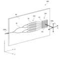
次に、図2Aを参照して、本実施形態における光偏向装置200の具体的な構成例を説明する。図2Aは、本実施形態における光偏向装置200の例を模式的に示す斜視図である。参考のために、互いに直交するX軸、Y軸、およびZ軸が模式的に示されている。光偏向装置200は、光導波路アレイ10Aと、位相シフタアレイ20Aと、光分岐器30と、それらが集積された基板40と、を備える。光導波路アレイ10Aは、Y方向に配列された複数の光導波路素子10を含む。各光導波路素子10はX方向に延びている。位相シフタアレイ20AはY方向に配列された複数の位相シフタ20を含む。各位相シフタ20はX方向に延びている。光導波路アレイ10Aにおける複数の光導波路素子10は、位相シフタアレイ20Aにおける複数の位相シフタ20にそれぞれ接続されている。位相シフタアレイ20Aには光分岐器30が接続されている。Next, referring to FIG. 2A, a specific configuration example of the
光源100から発せられた光ビーム100L0は、光分岐器30を介して位相シフタアレイ20Aにおける複数の位相シフタ20に入力する。位相シフタアレイ20Aにおける複数の位相シフタ20を通過した光は、位相がY方向に一定量ずつシフトした状態で、光導波路アレイ10Aにおける複数の光導波路素子10にそれぞれ入力する。光導波路アレイ10Aにおける複数の光導波路素子10にそれぞれ入力した光は、光ビーム100Lとして、XY平面に平行な光出射面10sから、光出射面10sに交差する方向に出射される。 A light beam100L0 emitted from a
次に、図2Bを参照して、本実施形態における光導波路素子10の具体的な構成例を説明する。図2Bは、本実施形態における光導波路素子10の例を模式的に示す図である。本実施形態における光導波路素子10は、互いに対向する第1ミラー10m1および第2ミラー10m2と、第1ミラー10m1と第2ミラー10m2との間に位置し、かつ、液晶材料を含む液晶層10lcと、液晶層10lcに第1駆動電圧を印加するための一対の第1電極10elとを含む。第1ミラー10m1の透過率は、第2ミラー10m2の透過率よりも高い。第1ミラー10m1および第2ミラー10m2の少なくとも一方は、例えば、複数の高屈折率層および複数の低屈折率層が交互に積層された多層反射膜から形成され得る。第1ミラー10m1および第2ミラー10m2は、同じ高屈折率層および同じ低屈折率層を含む多層反射膜から形成されてもよい。この場合、第1ミラー10m1の積層数を第2ミラー10m2の積層数よりも少なくすれば、第1ミラー10m1の透過率は、第2ミラー10m2の透過率よりも高くなる。 Next, a specific configuration example of the
光源100から出射された光ビーム100L0の一部10Lは、液晶層10lc内を第1ミラー10m1および第2ミラー10m2によって反射されながらX方向に沿って伝搬する。その際、液晶層10lc内を伝搬する光10Lの一部が第1ミラー10m1から外部に出射される。 A portion 10L of the light beam100L0 emitted from the
一対の第1電極10elに第1駆動電圧を印加することにより、液晶層10lcにおける液晶材料の屈折率が変化し、光導波路素子10から外部に出射される光の方向が変化する。第1駆動電圧の変化に対する液晶材料の屈折率の変化速度は、例えば30Hz以上120Hz以下であり得る。第1駆動電圧の変化に応じて、光導波路アレイ10Aから出射される光ビーム100Lの方向が変化する。具体的には、図2Aに示す例において、光ビーム100Lの出射方向と、YZ平面に平行な平面とがなす第1出射角度が変化する。本明細書では、第1出射角度が変化する方向を光出射面10sに投影した方向を、「第1方向D1」と称する。 By applying a first driving voltage to the pair of first electrodes 10el, the refractive index of the liquid crystal material in the liquid crystal layer 10lc changes, and the direction of the light emitted from the
次に、図2Cを参照して、本実施形態における位相シフタ20の具体的な構成例を説明する。図2Cは、本実施形態における位相シフタ20の例を模式的に示す図である。本実施形態における位相シフタ20は、熱によって屈折率が変化する熱光学材料を含む全反射導波路20wと、全反射導波路20wに熱的に接触するヒータ20hと、ヒータ20hに第2駆動電圧を印加するための一対の第2電極20elとを含む。全反射導波路20wの屈折率は、ヒータ20h、基板40および空気の屈折率よりも高い。屈折率差により、光源100から出射された光ビーム100L0の一部20Lは、全反射導波路20w内を全反射されながらX方向に沿って伝搬する。 Next, a specific configuration example of the
一対の第2電極20elに第2駆動電圧を印加することにより、全反射導波路20wがヒータ20hによって加熱される。その結果、全反射導波路20wの屈折率が変化し、全反射導波路20wの端から出力される光20Lの位相がシフトする。第2駆動電圧の変化に対する熱光学材料の屈折率の変化速度は、例えば1kHz以上10kHz以下であり得る。図2Aに示す例において、位相シフタアレイ20Aにおける複数の位相シフタ20から出力される光20Lの位相がY方向に沿って一定量ずつ増減すれば、光ビーム100Lの出射方向とXZ平面に平行な平面とがなす第2出射角度が変化する。本明細書では、第2出射角度が変化する方向を光出射面10sに投影した方向を、「第2方向D2」と称する。第1方向D1と第2方向D2は直交している。 By applying a second driving voltage to the pair of second electrodes 20el, the
本明細書において、「光ビーム100Lの照射位置」は、第1方向D1および第2方向D2に平行で光出射デバイスから所定の距離だけ離れた仮想的なスクリーンに向けて光ビームを出射したと仮定した場合に、当該仮想的なスクリーンが光ビームで照射される位置を意味する。仮想的なスクリーンは、計測対象領域に相当する。 In this specification, the "irradiation position of the
本実施形態における光偏向装置200の動作原理、および動作方法などの詳細は、米国特許出願公開第2018/0224709号に開示されている。この文献の開示内容全体を本明細書に援用する。Details of the operation principle and operation method of the
上記のように、液晶材料の屈折率および熱光学材料の屈折率の変化速度は異なる。この変化速度の違いにより、第1方向D1に沿った光ビーム100Lの方向の変化速度は、第2方向D2に沿った光ビーム100Lの方向の変化速度よりも低い。本明細書では、「第1方向D1に沿った光ビーム100Lの方向の変化速度」を、単に「第1方向D1の変化速度」と称し、「第2方向D2に沿った光ビーム100Lの方向の変化速度」を、単に「第2方向D2の変化速度」と称する。本実施形態では、光ビーム100Lを対象物に向けて効率よく出射するために、変化速度が相対的に低い第1方向D1に沿って光ビーム100Lの方向を変化させる動作が周期的に行われる。この点で、第1方向D1に沿って光ビーム100Lの方向を変化させる動作は、変化速度が相対的に高い第2方向D2に沿って光ビームの方向を変化させる動作とは異なっている。 As described above, the change rates of the refractive index of the liquid crystal material and the refractive index of the thermo-optical material are different. Due to this difference in change rate, the change rate of the direction of the
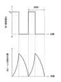
以下に、図3を参照して、光ビーム100Lの方向を第1方向D1に沿って変化させる動作の例を説明する。光ビーム100Lの方向を第2方向D2に沿って変化させる動作については後述する。図3は、第1駆動電圧の時間変化の例と、第1方向D1に沿って変化する光ビーム100Lの照射位置の時間変化の例とを模式的に示す図である。図3の上の図は、第1駆動電圧の時間変化の例を表し、下の図は、光ビーム100Lの照射位置の時間変化の例を表す。本実施形態では、図3の上の図に示すように、第1駆動電圧を一定時間オン(V0[V])にした後、一定時間オフ(0[V])にする動作が周期Tで繰り返される。このように、第1駆動電圧は、0[V]からV0[V]までの所定の範囲内で繰り返し変化する。本実施形態では、第1駆動電圧の変化は周期的であるが、厳密に周期的である必要はない。図3の下の図に示すように、第1駆動電圧がオンの間、光ビーム100Lの照射位置は時間経過とともに下に凸の曲線で正の方向に変化する。一方、第1駆動電圧がオフの間、光ビーム100Lの照射位置は時間経過とともに上に凸の曲線で負の方向に変化する。 An example of the operation of changing the direction of the
次に、図4Aおよび図4Bを参照して、光ビーム100Lの照射位置の第1方向D1に沿った移動速度を説明する。図4Aおよび図4Bは、第1駆動電圧を変化させたときの変化前後の電圧差と光ビーム100Lの照射位置の移動速度との関係の例を模式的に示す図である。図4Aは、第1駆動電圧が0[V]から増加した場合の電圧差に対する移動速度の依存性の例を示している。図4Bは、第1駆動電圧がV0[V]から減少した場合の電圧差に対する移動速度の依存性の例を示している。 Next, the moving speed of the irradiation position of the
図4Aに示すように、第1駆動電圧の初期値が0[V]のとき、光ビーム100Lの移動速度は、電圧差ΔVの増加に伴って上に凸の曲線で増加し、電圧差ΔV=V0で飽和する。第1駆動電圧が0[V]からV0[V]に増加したとき(電圧差ΔV=V0)、光ビーム100Lの照射位置の正の方向における移動速度が最も高い。図4Bに示すように、第1駆動電圧の初期値がV=V0[V]のとき、光ビーム100Lの移動速度は、電圧差ΔVの増加に伴って下に凸の曲線で増加する。第1駆動電圧がV=V0[V]からV=0[V]に減少したとき(電圧差ΔV=V0)、光ビーム100Lの照射位置の負の方向における移動速度が最も高い。 As shown in FIG. 4A, when the initial value of the first driving voltage is 0 [V], the moving speed of the
図5は、光ビーム100Lの照射位置を第1方向に沿って位置する対象物A、B、およびCに移動させる2つの動作を説明するための図である。ここでは簡単のため、対象物は一点に位置するとする。実際には、対象物は大きさを有する。本明細書において、「対象物の位置」は、一点の位置を示すとは限らず、その対象物が占める領域の位置を意味する。図5の上の図は、第1駆動電圧の時間変化の例を表し、下の図は、第1方向D1における光ビーム100Lの照射位置の時間変化の例を表す。図5に示す実線は、図3に示す実線と同じであり、本実施形態における第1駆動電圧の時間変化の例を示している。図5に示す破線は、光ビーム100Lが対象物A、B、およびCの位置に収束する第1駆動電圧をそれぞれ印加したと仮定した場合における波形を示している。図5の下の図に示すように、実線で示す本実施形態における駆動方法の方が、破線で示す駆動方法よりも短時間で対象物A、B、およびCに光ビーム100Lが到達することがわかる。これは、図4Aおよび図4Bを参照して説明したように、第1駆動電圧をオンおよびオフにする際の電圧差ΔVが大きいほど、光ビーム100Lの移動速度が高くなるからである。各対象物の位置に光ビームが収束する第1駆動電圧を印加する場合、電圧差ΔVが最大値V0よりも小さいので、光ビーム100Lの移動速度は、電圧差ΔVが最大値V0の場合よりも低い。このように、本実施形態では、第1駆動電圧を十分に大きい振幅で周期的に印加することにより、第1方向D1に沿った光ビームの移動速度を高くすることができる。 FIG. 5 is a diagram for explaining two operations for moving the irradiation position of the
図6は、光ビーム100Lの照射位置が対象物の位置に収束する様子の例を模式的に示す図である。図6に示すように、対象物の位置に光ビーム100Lが収束する第1駆動電圧を印加する場合、光ビーム100Lの照射位置がその位置に実際に収束するまでに長い時間を要する。収束に要する時間は、光ビーム100Lの移動前後の照射位置の差に依存する。照射位置の差が大きく、変化前後の電圧差が大きいほど収束時間が長くなり、電圧差が小さいほど収束時間が短くなる。本実施形態では、第1駆動電圧をオン・オフする動作を周期的に繰り返すことにより、光ビーム100Lの照射位置は対象物の位置を比較的高い速度で通過する。図3に示すような、第1駆動電圧の時間変化と光ビーム100Lの照射位置の時間変化との対応関係を予め把握していれば、動作中の第1駆動電圧の時間変化から、光ビーム100Lの照射位置を知ることができる。Figure 6 is a schematic diagram showing an example of how the irradiation position of the
光ビーム100Lは常に出射されている必要はない。本実施形態では、光ビーム100Lが出射された場合に光ビーム100Lの照射位置が対象物の位置に一致するタイミングで、制御回路500は、光源100に光ビーム100L0を出射させる。言い換えれば、制御回路500は、第1駆動電圧が、0[V]からV0[V]までの所定の範囲内に含まれる特定の範囲内にある場合に限り、光源100に光ビーム100L0を出射させる。ここで、「照射位置が対象物の位置に一致するタイミング」は、光ビームを出射したと仮定した場合に、その対象物の少なくとも一部が光ビームで照射されるタイミングを意味する。 The
次に、図7を参照して、第1駆動電圧を印加する動作の他の例を説明する。図7は、第1駆動電圧の時間変化の他の例を模式的に示す図である。図7に示すように、図3の上の図に示す第1駆動電圧に高周波を重畳してもよい。図7に示す例では、一定時間内に正負の振幅を有する矩形形状の電圧が7回印加されている。当該矩形状の電圧の代わりに、正弦波形状の電圧が印加されてもよい。図3の上の図に示すように正の電圧を印加し続けると、一対の第1電極10elのうち、一方の電極に正イオンが、他方の電極に負イオンが一定時間帯電し続ける。このような状態が続くと、一対の第1電極10elが早期に劣化し、所定の電圧を印加できなくなる可能性がある。図7に示すように、正負の電圧を高速で印加することにより、一対の第1電極10elの上記の劣化を抑制することができる。図7に示すように第1駆動電圧を印加しても、光ビーム100Lの照射位置は、図3の下の図に示すように変化する。Next, referring to FIG. 7, another example of the operation of applying the first driving voltage will be described. FIG. 7 is a diagram showing another example of the time change of the first driving voltage. As shown in FIG. 7, a high frequency may be superimposed on the first driving voltage shown in the upper diagram of FIG. 3. In the example shown in FIG. 7, a rectangular voltage having positive and negative amplitudes is applied seven times within a certain time. Instead of the rectangular voltage, a sinusoidal voltage may be applied. If a positive voltage is continuously applied as shown in the upper diagram of FIG. 3, one of the pair of first electrodes 10el continues to be charged with positive ions and the other electrode continues to be charged with negative ions for a certain time. If such a state continues, the pair of first electrodes 10el may deteriorate early and a predetermined voltage may not be applied. As shown in FIG. 7, the above-mentioned deterioration of the pair of first electrodes 10el can be suppressed by applying positive and negative voltages at high speed. Even if the first driving voltage is applied as shown in FIG. 7, the irradiation position of the
次に、図8を参照して、光ビーム100Lの形状を説明する。図8は、光ビーム100Lの形状の例を模式的に示す図である。図8の左端の図に示すように、光ビーム100Lの形状は、広がり角が回折限界によって決まる程度の円形あってもよい。ここで、広がり角とは、光ビーム100Lが両側に広がる角度を意味する。図8の左から2番目の図に示すように、光ビーム100Lの形状は、広がり角が回折限界以上2度以下の円形であってもよい。図8の左から3番目および4番目の図に示すように、光ビーム100Lの形状は、楕円形であってもよい。一方向のスキャンによって前述の仮想的なスクリーン全体を照射するラインスキャンでは、長径方向の広がり角が30度以上150度以下であり、短径方向の広がり角が回折限界以上2度以下である楕円形または線形であってもよい。このように、本実施形態における光ビーム100Lの形状は任意であり、用途および対象物の大きさに応じて決定され得る。一度に複数の光ビーム100Lが照射されてもよい。Next, the shape of the
以下に、図9および図10を参照して、本実施形態における、光ビーム100Lの方向を第1方向D1および第2方向D2に沿って変化させる動作の例を説明する。図9は、制御回路500の動作の例を示すフローチャートである。図9に示すように、ステップS101において、制御回路500は、光源100が非発光の状態で、第1駆動電圧を所定の範囲内で繰り返し変化させる動作を開始する。図3の上の図に示す例では、所定の範囲は、ゼロから正の電圧までの範囲である。ステップS102において、制御回路500は、画像データを撮像装置300から取得する。ステップS103において、制御回路500は、撮像装置300から取得した画像データに基づいて、対象物の位置、第2駆動電圧の変化のさせ方、および光ビーム100L0の出射タイミングを決定する。ステップS104において、制御回路500は、光ビーム100Lが出射された場合に画像データから認識された特定の1以上の対象物が光ビーム100Lで照射されるように、対象物の位置に応じて第2駆動電圧を変化させる。ステップS105において、制御回路500は、決定した出射タイミングに基づいて、光源100に光ビーム100L0を出射させる。この出射タイミングは、1以上の対象物が光ビーム100Lで照射されるタイミングである。制御回路500は、このタイミング以外では、光源100に光ビーム100L0の出射を停止させる。制御回路500は、第1駆動電圧を変化させている期間に、対象物ごとに、ステップS104およびステップS105の動作を実行する。なお、図5の下の図に示すように光ビーム100Lの方向を第1方向D1に沿ってのみ変化させる場合、ステップS103における第2駆動電圧の変化のさせ方を決定する動作、およびステップS104の動作は省略される。 Hereinafter, with reference to FIG. 9 and FIG. 10, an example of the operation of changing the direction of the
図10は、図9に示す動作を実行した場合における、光ビーム100Lの照射位置の軌跡と対象物の位置との関係の例を模式的に示す図である。図10に示す矩形領域は、前述の仮想的なスクリーンを示している。仮想的なスクリーンにおける矢印付きの実線は、光ビーム100Lの照射位置の軌跡を表し、楕円は対象物の位置を表す。3つの対象物の位置は、ステップS103において決定される。光ビーム100Lの照射位置が対象物の位置に一致するときのみ、光源100から光ビーム100L0が出射される。光偏向装置200によって方向が変化した光ビーム100Lの照射位置は、それぞれの対象物の全体をスキャンするために第2方向に沿って細かく往復するように制御され得る。第2方向D2の変化速度は、第1方向D1の変化速度よりも高いので、このような動作が実現できる。この動作では、制御回路500は、光ビーム100Lの方向の第2方向D2の成分を増減させながら、光源100に光ビーム100L0を複数回出射させる。制御回路500は、受光デバイス400に、対象物からの反射光を検出させる。制御回路500は、受光デバイス400からの信号に基づいて、対象物までの距離を計測する。 FIG. 10 is a diagram showing an example of the relationship between the locus of the irradiation position of the
本実施形態では、制御回路500は、変化速度が相対的に低い第1方向D1に沿って光ビーム100Lの方向を繰り返し変化させる途中で、変化速度が相対的に高い第2方向D2に沿って光ビーム100Lの方向を1以上の対象物の位置に応じて変化させる。制御回路500のこの動作により、シーン全体をスキャンすることなく、1以上の対象物までの距離を短時間で計測することができる。本実施形態における仮想的なスクリーンの第2方向D2に沿ったサイズは、第1方向D1に沿ったサイズよりも大きい。変化速度が相対的に高い第2方向D2方向に沿ったサイズが大きい方が、1以上の対象物までの距離を短時間で計測することができる。 In this embodiment, the
次に、図11から図13を参照して、本実施形態における、光ビーム100Lを第1方向D1および第2方向D2に沿って変化させる動作の他の例を説明する。図11は、制御回路500の動作の他の例を示すフローチャートである。ステップS201およびステップS202は、それぞれ図9に示すステップS101およびステップS102と同じである。ステップS203において、制御回路500は、撮像装置300から取得した画像データに基づいて、1以上の対象物の位置および優先順位を決定する。優先順位は、例えば、対象物が人である確率、または測距装置である撮像装置300によって計測された対象物までのおおよその距離に基づいて決定され得る。対象物が人である確率が高い場合、または対象物までのおおよその距離が短い場合、当該対象物の優先順位を高く設定してもよい。対象物が人である確率が低い場合、または対象物までのおおよその距離が所定の距離よりも長い場合、当該対象物を計測対象から除外してもよい。また、例えば以下の条件に合致する対象物の優先順位を高く設定してもよい。(a)対象物が自車両の進路上に検知された場合、(b)対象物の認識が不能だった場合。(a)および(b)は、撮像装置300から取得した画像データにおける直前の1フレームを用いた画像認識の結果、および自車の走行計画情報に基づき、公知の手段により判定することができる。他には、以下の条件に合致する対象物の優先順位を高く設定してもよい。(c)対象物の進行方向が自車両に向かっている場合、(d)対象物の予測進路が自車両の進路と交差する場合、(e)対象物のモーションベクトルの変化が所定の基準よりも大きい場合。(c)~(e)は、撮像装置300から取得した画像データにおける複数フレームを用いて公知の手段により算出した、対象物のモーションベクトルに基づき判定することができる。以上に挙げた複数の条件から選択された任意の組合せに対して所定の重み付けを行い、最終的な1以上の対象物の優先順位を決定する。ステップS204において、制御回路500は、ステップS203において決定した優先順位に基づいて、対象物の計測順序、第2駆動電圧の変化のさせ方、および光ビーム100Lの出射タイミングを決定する。ステップS205およびステップS206は、図9に示すステップS104およびステップS105と同じである。制御回路500は、対象物ごとに、ステップS205およびステップS206の動作を実行する。画像データが随時更新される場合、制御回路500は、ステップS202からステップS206の動作を繰り返し実行し得る。 Next, with reference to FIG. 11 to FIG. 13, another example of the operation of changing the
図12Aは、ステップS202において取得された画像データから認識された対象物AからFの配置の例を模式的に示す図である。図12Aにおける×印は、光ビーム100Lの現在の照射位置を表している。図12Bおよび図12Cは、それぞれ、ステップS203およびステップS204において決定された情報の例を示す図である。Figure 12A is a diagram showing a schematic example of the arrangement of objects A to F recognized from the image data acquired in step S202. The cross marks in Figure 12A represent the current irradiation position of
図12Bに示すように、制御回路500は、対象物DおよびFを例えば人ではないと判定し、これらの対象物を計測対象から除外する。制御回路500は、それ以外の対象物の優先順位を付け、対象物の位置に座標を付与する。図12Bに示す例では、対象物Eの優先順位が最も高く、対象物Cの優先順位が2番目に高く、対象物Aの優先順位が3番目に高く、および対象物Bの優先順位が最も低い。対象物Aの位置の座標は(Xa、Ya)である。Xaは、不図示の原点から対象物Aの位置までの距離を第1方向D1に平行な線に正射影した第1成分であり、Yaは、不図示の原点から対象物Aの位置までの距離を第2方向D2に平行な線に正射影した第2成分である。他の対象物の座標についても同様である。除外された対象物の座標は、必ずしも決定しなくてもよい。 As shown in FIG. 12B, the
図12Cに示すように、制御回路500は、対象物の計測順序を決定する。計測順序は、光ビーム100Lの現在の照射位置の座標における第1成分と、対象物の位置の座標における第1成分との差が小さい順に決定される。ただし、対象物Bおよび対象物Cのように複数の対象物の位置の座標における第1成分が一致するときは、優先順位の高い対象物の計測順序が先になる。優先順位が低い対象物は、光ビーム100Lが次に通過するときに計測される。図12Cに示す例では、対象物Aの計測順序が1番目であり、対象物Cの計測順序が2番目であり、対象物Eの計測順序が3番目であり、対象物Bの計測順序が4番目である。光ビーム100Lの照射位置を対象物Aの位置まで変化させるための第2駆動電圧はVaであり、対象物Aを照射するための出射タイミングはTaである。出射タイミングは、例えば最初に計測を開始してからの時間である。他の対象物の第2駆動電圧および出射タイミングについても同様である。 As shown in FIG. 12C, the
図13は、図11に示す動作を実行した場合における、光ビーム100Lの照射位置の軌跡と対象物の位置との関係の例を模式的に示す図である。仮想的なスクリーンにおける矢印付きの実線は、光ビーム100Lの照射位置の軌跡を表す。図13に示すように、光ビーム100Lの照射位置は、対象物A、C、およびEを通過した後、折り返して対象物Bを通過する。第1方向D1における光ビーム100Lの照射位置は周期的に変化する。光ビーム100Lの照射位置が対象物の位置に一致するときのみ、光源100から光ビーム100L0が出射される。このように、制御回路500は、光ビーム100Lの方向の第2方向D2の成分を変化させながら、光源100に光ビーム100L0を複数回出射させて複数の対象物を順次照射する。 FIG. 13 is a diagram showing an example of the relationship between the trajectory of the irradiation position of the
対象物の優先順位は、すべての対象物までの距離を計測し終える前に随時更新してもよい。実際には、対象物は光ビーム100Lの形状よりも大きい場合が多い。対象物全体を照射するために、図12Cに示す第2駆動電圧および出射タイミングは、ある程度の幅を有していてもよい。あるいは、図10に示すように、光ビーム100Lの照射位置は、それぞれの対象物の全体をスキャンするために第2方向に沿って細かく往復してもよい。The priority of the objects may be updated at any time before the distances to all the objects are measured. In reality, the objects are often larger than the shape of the
(光偏向装置200の変形例)
次に、図14Aおよび図14Bを参照して、本実施形態における光偏向装置200の変形例を説明する。図14Aは、本実施形態の変形例における光偏向装置210の例を模式的に示す斜視図である。本実施形態の変形例における光偏向装置210は、電磁式のMEMSミラーを備える。本実施形態の変形例における光偏向装置210は、ミラー210mと、ミラー210mを第1トーションバー210t1によって支持する内側フレーム210f1と、内側フレーム210f1を第2トーションバー210t2によって支持する外側フレーム210f2とを備える。トーションバーは、ねじったときに反発力が働くバネの一種である。ミラー210mは、内側フレーム210f1内で、X方向に平行な第1トーションバー210t1を回転軸として回転する。内側フレーム210f1は、外側フレーム210f2内で、Y方向に平行な第2トーションバー210t2を回転軸として回転する。内側フレーム210f1の外縁部に沿って、第1配線210w1が取り付けられ、ミラー210mの外縁部に沿って第2配線210w2が取り付けられている。第1配線210w1は、その両端に一対の第1電極210el1を有し、第2配線210w2は、その両端に一対の第2電極210el2を有する。XY平面に平行な方向に、磁場が印加されている。光源100から発せられた光ビーム100L0は、ミラー210mによって反射され、光ビーム100Lとして外部に出射される。 (Modification of the optical deflection device 200)
Next, a modified example of the
一対の第1電極210el1に第1駆動電圧を印加すると、第1配線210w1に電流が流れる。第1配線210w1のうち、Y方向に延びる部分に流れる電流IYまたは-IYと、磁場のX方向に平行な成分BXとにより、Y方向に延びる当該部分には、Z方向に平行なローレンツ力-F1ZまたはF1Zが働く。その結果、内側フレーム210f1はY軸を回転軸として回転し、光ビーム100Lの方向は第1方向D1に沿って変化する。同様に、一対の第2電極210el2に第2駆動電圧を印加すると、第2配線210w2に電流が流れる。第2配線210w2のうち、X方向に延びる部分に流れる電流IXまたは-IXと、磁場のY方向に平行な成分BYとにより、X方向に延びる当該部分には、Z方向に平行なローレンツ力-F2ZまたはF2Zが働く。その結果、ミラー210mはX軸を回転軸として回転し、光ビーム100Lの方向は第2方向D2に沿って変化する。以上のように、第1駆動電圧および第2駆動電圧の変化に応じてMEMSミラーの方向が変化することにより、ミラー210mによって反射される光ビーム100Lの方向が第1方向D1および第2方向D2に沿ってそれぞれ変化する。 When a first driving voltage is applied to thepair of first electrodes210el1 , a current flows through the first wiring210w1 . Due to the currentIY or-IY flowing through the portion of the first wiring 210w1 extending in the Y direction and the componentBX of the magnetic field parallel to the X direction, a Lorentz force-F1Z orF1Z parallel to the Z direction acts on the portion extending in the Y direction. As a result, the inner frame210f1 rotates around the Y axis as the rotation axis, and the direction of the
ミラー210mを支持する内側フレーム210f1のY軸を回転軸とした回転速度は、ミラー210mのX軸を回転軸とした回転速度よりも低い。ミラー210mおよび内側フレーム210f1の合計の重さは、ミラー210mの重さよりも重いからである。したがって、変形例における光偏向装置210でも、第1方向D1の変化速度は、第2方向D2の変化速度よりも低い。第1方向D1の変化速度は、例えば10Hz以上500Hz以下であり、第2方向D2の変化速度は、例えば50Hz以上1kHz以下であり得る。この場合でも、図9および図11に示す制御回路500の動作により、対象物までの距離を短時間で計測することができる。 The rotation speed of the inner frame 210f1 supporting the
図14Bは、図14Aの光偏向装置210における一対の第1電極210el1に印加される第1駆動電圧の時間変化の例を模式的に示す図である。図14Bに示す例では、正の電圧が一定時間印加された後、負の電圧が一定時間印加される動作が周期的に繰り返される。言い換えれば、第1駆動電圧は、負の電圧から正の電圧までの所定の範囲で繰り返し周期的に変化する。負の電圧と正の電圧の絶対値は等しくてもよいし、異なっていてもよい。図3の上の図に示す例とは異なり負の電圧を印加するのは、第1配線210w1のY方向に延びる部分に流れる電流の向きを変えてローレンツ力の向きを反転させることにより、光ビーム100Lの方向を第1方向D1に沿って大きく変化させるためである。 FIG. 14B is a diagram showing an example of the time change of the first driving voltage applied to the pair of first electrodes 210el1 in the
光偏向装置は、電磁式のMEMSミラーの代わりに、静電式のMEMSミラーを備えていてもよい。静電式のMEMSミラーでは、電極間に働く引力を利用してMEMSミラーが回転する。静電式のMEMSミラーでも、電磁式のMEMSミラーと同様の理由により、交差する2つの方向のうち、一方の方向の変化速度は、他方の方向の変化速度よりも低い。低い方の変化速度は、例えば10Hz以上500Hz以下であり、高い方の変化速度は、例えば50Hz以上1kHz以下であり得る。The optical deflection device may be equipped with an electrostatic MEMS mirror instead of an electromagnetic MEMS mirror. In an electrostatic MEMS mirror, the MEMS mirror rotates by utilizing the attractive force acting between electrodes. For the same reason as in the electromagnetic MEMS mirror, the electrostatic MEMS mirror has a lower rate of change in one of the two intersecting directions than in the other direction. The lower rate of change may be, for example, 10 Hz or more and 500 Hz or less, and the higher rate of change may be, for example, 50 Hz or more and 1 kHz or less.
(応用例)
次に、図15を参照して、本実施形態における光検出システム1000の応用例を説明する。図15は、光検出システム1000を備える車両600を模式的に示す図である。仮想的なスクリーンにおける矢印付きの実線は、光ビーム100Lの照射位置の軌跡を表す。図15に示すように、光検出システム1000は車両600に取り付けられて使用され得る。光検出システム1000は、道路610上の車両600の前方にいる人を対象物として、対象物までの距離を計測する。車両600の前方において4人の歩行者が道路610を横切る場合、歩行者を対象物として仮想的なスクリーンに投影すると、対象物AからDによって表される4つの対象物が、道路610の水平面にほぼ平行に並んで位置する。図15に示す例では、変化速度が相対的に低い第1方向D1が道路610の水平面にほぼ平行である。本実施形態における制御回路500の動作を実行すれば、軌跡に示すように、光ビーム100Lの方向を第1方向D1に沿って1回だけ変化させる間に、光ビーム100Lの方向を第2方向D2に沿って少し変化させるだけで、すべての対象物までの距離を短時間で計測することができる。第1方向D1は、必ずしも道路610の水平面にほぼ平行である必要はない。第1方向D1と道路610の水平面とがなす角度が例えば0度以上45度以下であっても、対象物までの距離を比較的短時間で計測することができる。 (Application example)
Next, an application example of the
本開示の実施形態における光出射デバイス、光検出システム、および車両は、例えば対象物までの距離を計測する用途に利用できる。The light emitting devices, light detection systems, and vehicles of the embodiments of the present disclosure can be used, for example, to measure the distance to an object.
10 光導波路素子
10A 光導波路アレイ
10L 光ビームの一部
10el 第1電極
10lc 液晶層
10m1 第1ミラー
10m2 第2ミラー
20 位相シフタ
20A 位相シフタアレイ
20L 光ビームの一部
20el 第2電極
20h ヒータ
20w 全反射導波路
30 光分岐器
40 基板
100 光源
100L0、100L 光ビーム
200、210 光偏向装置
210el1 第1電極
210el2 第2電極
210f1 内側フレーム
210f2 外側フレーム
210m ミラー
210w1 第1配線
210w2 第2配線
300 撮像装置
400 受光デバイス
500 制御回路
600 車両
610 道路
1000 光検出システム 10
Claims (13)
Translated fromJapanese入力された駆動電圧に応答して前記光ビームの方向を変化させる光偏向装置と、
前記光源に前記制御信号を入力し、前記光偏向装置に前記駆動電圧を入力することにより、前記光ビームの出射タイミングおよび前記光ビームの方向を制御する制御回路と、
を備え、
前記光偏向装置は、
前記光ビームの方向を、第1方向と、前記第1方向とは異なる第2方向に沿って変化させることが可能であり、
前記第1方向に沿った前記光ビームの方向の変化速度は、前記第2方向に沿った前記光ビームの方向の変化速度よりも低く、
前記制御回路は、
前記駆動電圧により前記光ビームの方向の前記第1方向の成分を周期的に変化させている期間に、1以上の対象物の位置に応じて、前記光ビームの方向の前記第2方向の成分を変化させる、
光出射デバイス。 a light source that emits a light beam in response to an input control signal;
an optical deflection device that changes the direction of the optical beam in response to an input drive voltage;
a control circuit that controls an emission timing and a direction of the light beam by inputting the control signal to the light source and inputting the drive voltage to the optical deflection device;
Equipped with
The optical deflection device includes:
the direction of the light beam can be varied along a first direction and a second direction different from the first direction;
a rate of change of direction of the light beam along the first direction is less than a rate of change of direction of the light beam along the second direction;
The control circuit includes:
changing a second directional component of the direction of the light beam in response to positions of one or more objects during a period in which the first directional component of the direction of the light beam is periodically changed by the driving voltage;
Light emitting device.
互いに対向する第1および第2の多層反射膜と、
前記第1および第2の多層反射膜の間に位置する液晶層と、
前記液晶層に前記駆動電圧を印加するための2つの電極と、
を備え、
前記光源から出射された前記光ビームは、前記液晶層内を伝搬し、前記第1の多層反射膜から出射され、
前記駆動電圧の変化に応じて、前記第1の多層反射膜から出射される前記光ビームの方向が変化する、
請求項1または2に記載の光出射デバイス。 The optical deflection device includes:
first and second multilayer reflective films facing each other;
a liquid crystal layer located between the first and second multilayer reflective films;
two electrodes for applying the driving voltage to the liquid crystal layer;
Equipped with
the light beam emitted from the light source propagates through the liquid crystal layer and is emitted from the first multilayer reflective film;
a direction of the light beam emitted from the first multilayer reflective film is changed in response to a change in the driving voltage;
3. A light emitting device according to claim 1 or 2.
前記MEMSミラーは、前記駆動電圧の印加によって回転し、
前記駆動電圧の変化に応じて前記MEMSミラーの方向が変化することにより、反射された前記光ビームの方向が変化する、
請求項1から3のいずれかに記載の光出射デバイス。 the optical deflection device includes a MEMS mirror that reflects the light beam emitted from the light source,
The MEMS mirror rotates in response to application of the driving voltage;
A change in orientation of the MEMS mirror in response to a change in the drive voltage changes the direction of the reflected light beam.
A light emitting device according to any one of claims 1 to 3.
請求項1に記載の光出射デバイス。 The first direction and the second direction are perpendicular to each other.
2. The light emitting device according to claim 1.
前記車両に取り付けられた状態において、
前記第1方向を含む平面と水平面とがなす角度は、0度以上45度以下である、
請求項1から6のいずれかに記載の光出射デバイス。 The light emitting device is attached to a vehicle for use,
When installed in the vehicle,
The angle between a plane including the first direction and a horizontal plane is greater than or equal to 0 degrees and less than or equal to 45 degrees.
A light emitting device according to any one of the preceding claims.
前記1以上の対象物からの反射光を検出する受光デバイスと、
を備える光検出システム。 A light emitting device according to any one of claims 1 to 7,
a light receiving device for detecting reflected light from the one or more objects;
1. A light detection system comprising:
前記制御回路は、
撮像装置から前記複数の対象物を含むシーンの画像データを取得し、
前記画像データから認識された前記複数の対象物の優先度を決定し、
前記駆動電圧を変化させている期間に、前記複数の対象物の位置および前記優先度に応じて、前記光ビームの方向の前記第2方向の成分を変化させる、
請求項1に記載の光出射デバイス。 the one or more objects include a plurality of objects;
The control circuit includes:
acquiring image data of a scene including the plurality of objects from an imaging device;
determining a priority of the plurality of objects recognized from the image data;
changing a component of the direction of the light beam in the second direction according to positions and the priorities of the plurality of objects during a period in which the driving voltage is being changed;
2. The light emitting device according to claim 1.
前記光出射デバイスは、
入力された制御信号に応答して光ビームを発する光源と、
入力された駆動電圧に応答して前記光ビームの方向を変化させる光偏向装置と、を備え、
前記光偏向装置は、
前記光ビームの方向を、第1方向と、前記第1方向とは異なる第2方向に沿って変化させることが可能であり、
前記第1方向に沿った前記光ビームの方向の変化速度は、前記第2方向に沿った前記光ビームの方向の変化速度よりも低く、
前記制御方法は、
前記駆動電圧により前記光ビームの方向の前記第1方向の成分を周期的に変化させている期間に、1以上の対象物の位置に応じて、前記光ビームの方向の前記第2方向の成分を変化させること、を含む、
制御方法。 A method for controlling a light emitting device, comprising the steps of:
The light emitting device comprises:
a light source that emits a light beam in response to an input control signal;
an optical deflection device that changes the direction of the optical beam in response to an input drive voltage;
The optical deflection device includes:
the direction of the light beam can be varied along a first direction and a second direction different from the first direction;
a rate of change of direction of the light beam along the first direction is less than a rate of change of direction of the light beam along the second direction;
The control method includes:
changing a second directional component of the direction of the light beam in response to a position of one or more objects during a period in which the first directional component of the direction of the light beam is periodically changed by the driving voltage.
Control methods.
前記光出射デバイスは、
入力された制御信号に応答して光ビームを発する光源と、
入力された駆動電圧に応答して前記光ビームの方向を変化させる光偏向装置と、を備え、
前記光偏向装置は、
前記光ビームの方向を、第1方向と、前記第1方向とは異なる第2方向に沿って変化させることが可能であり、
前記第1方向に沿った前記光ビームの方向の変化速度は、前記第2方向に沿った前記光ビームの方向の変化速度よりも低く、
前記コンピュータに、
前記駆動電圧により前記光ビームの方向の前記第1方向の成分を周期的に変化させている期間に、1以上の対象物の位置に応じて、前記光ビームの方向の前記第2方向の成分を変化させること、を実行させる、
コンピュータプログラム。 A computer program executed on a computer that controls a light emitting device,
The light emitting device comprises:
a light source that emits a light beam in response to an input control signal;
an optical deflection device that changes the direction of the optical beam in response to an input drive voltage;
The optical deflection device includes:
the direction of the light beam can be varied along a first direction and a second direction different from the first direction;
a rate of change of direction of the light beam along the first direction is less than a rate of change of direction of the light beam along the second direction;
The computer includes:
changing a second directional component of the direction of the light beam in response to positions of one or more objects during a period in which the first directional component of the direction of the light beam is periodically changed by the driving voltage;
Computer program.
Applications Claiming Priority (3)
| Application Number | Priority Date | Filing Date | Title |
|---|---|---|---|
| JP2019162292 | 2019-09-05 | ||
| JP2019162292 | 2019-09-05 | ||
| PCT/JP2020/029911WO2021044792A1 (en) | 2019-09-05 | 2020-08-05 | Light emission device, light detection system, and vehicle |
Publications (3)
| Publication Number | Publication Date |
|---|---|
| JPWO2021044792A1 JPWO2021044792A1 (en) | 2021-03-11 |
| JPWO2021044792A5 JPWO2021044792A5 (en) | 2022-05-20 |
| JP7595259B2true JP7595259B2 (en) | 2024-12-06 |
Family
ID=74852853
Family Applications (1)
| Application Number | Title | Priority Date | Filing Date |
|---|---|---|---|
| JP2021543663AActiveJP7595259B2 (en) | 2019-09-05 | 2020-08-05 | Light emitting device, light detection system, and vehicle |
Country Status (3)
| Country | Link |
|---|---|
| US (1) | US12422528B2 (en) |
| JP (1) | JP7595259B2 (en) |
| WO (1) | WO2021044792A1 (en) |
Citations (7)
| Publication number | Priority date | Publication date | Assignee | Title |
|---|---|---|---|---|
| JP2007187618A (en) | 2006-01-16 | 2007-07-26 | Omron Corp | Object identifying device |
| JP2009002978A (en) | 2007-06-19 | 2009-01-08 | Konica Minolta Opto Inc | Microscanner and optical scanner equipped with the same |
| JP2017181209A (en) | 2016-03-29 | 2017-10-05 | 富士通株式会社 | Distance measuring device, distance measuring method, and program |
| JP2018124271A (en) | 2017-01-31 | 2018-08-09 | パナソニックIpマネジメント株式会社 | Imaging System |
| JP2018128663A (en) | 2017-02-09 | 2018-08-16 | パナソニックIpマネジメント株式会社 | Optical scanning device, optical receiving device, and optical detection system |
| US20180275274A1 (en) | 2017-03-23 | 2018-09-27 | Innovusion Ireland Limited | High resolution lidar using multi-stage multi-phase signal modulation, integration, sampling, and analysis |
| US10302746B2 (en) | 2016-05-18 | 2019-05-28 | James Thomas O'Keeffe | LIDAR system with vehicle-integrated beam guide |
Family Cites Families (13)
| Publication number | Priority date | Publication date | Assignee | Title |
|---|---|---|---|---|
| US7619739B1 (en)* | 2002-08-29 | 2009-11-17 | Science Applications International Corporation | Detection and identification of biological agents using Bragg filters |
| US8905610B2 (en)* | 2009-01-26 | 2014-12-09 | Flex Lighting Ii, Llc | Light emitting device comprising a lightguide film |
| WO2012093654A1 (en)* | 2011-01-05 | 2012-07-12 | 日本電信電話株式会社 | Wavelength sweep light source |
| JP2013061488A (en) | 2011-09-13 | 2013-04-04 | Ricoh Co Ltd | Optical scanner |
| US10151960B2 (en)* | 2015-09-25 | 2018-12-11 | Microsoft Technology Licensing, Llc | Backlight assembly with tunable grating layer for local dimming |
| WO2017072634A1 (en)* | 2015-10-30 | 2017-05-04 | Semiconductor Energy Laboratory Co., Ltd. | Display device, electronic device, and method for manufacturing display device and electronic device |
| US10578719B2 (en)* | 2016-05-18 | 2020-03-03 | James Thomas O'Keeffe | Vehicle-integrated LIDAR system |
| EP4194887A1 (en)* | 2016-09-20 | 2023-06-14 | Innoviz Technologies Ltd. | Lidar systems and methods |
| KR102719930B1 (en)* | 2017-01-23 | 2024-10-23 | 삼성전자주식회사 | Method and apparatus for generating an image representing an object around a vehicle |
| CN108415205B (en) | 2017-02-09 | 2022-11-04 | 松下知识产权经营株式会社 | Optical scanning equipment, optical receiving equipment and optical detection system |
| JP7117092B2 (en) | 2017-09-25 | 2022-08-12 | 株式会社トプコン | LASER MEASUREMENT METHOD AND LASER MEASUREMENT DEVICE |
| US11415676B2 (en)* | 2017-10-09 | 2022-08-16 | Luminar, Llc | Interlaced scan patterns for lidar system |
| KR101947404B1 (en)* | 2018-05-14 | 2019-02-13 | 주식회사 에스오에스랩 | A lidar device |
- 2020
- 2020-08-05JPJP2021543663Apatent/JP7595259B2/enactiveActive
- 2020-08-05WOPCT/JP2020/029911patent/WO2021044792A1/ennot_activeCeased
- 2021
- 2021-12-07USUS17/544,750patent/US12422528B2/enactiveActive
Patent Citations (7)
| Publication number | Priority date | Publication date | Assignee | Title |
|---|---|---|---|---|
| JP2007187618A (en) | 2006-01-16 | 2007-07-26 | Omron Corp | Object identifying device |
| JP2009002978A (en) | 2007-06-19 | 2009-01-08 | Konica Minolta Opto Inc | Microscanner and optical scanner equipped with the same |
| JP2017181209A (en) | 2016-03-29 | 2017-10-05 | 富士通株式会社 | Distance measuring device, distance measuring method, and program |
| US10302746B2 (en) | 2016-05-18 | 2019-05-28 | James Thomas O'Keeffe | LIDAR system with vehicle-integrated beam guide |
| JP2018124271A (en) | 2017-01-31 | 2018-08-09 | パナソニックIpマネジメント株式会社 | Imaging System |
| JP2018128663A (en) | 2017-02-09 | 2018-08-16 | パナソニックIpマネジメント株式会社 | Optical scanning device, optical receiving device, and optical detection system |
| US20180275274A1 (en) | 2017-03-23 | 2018-09-27 | Innovusion Ireland Limited | High resolution lidar using multi-stage multi-phase signal modulation, integration, sampling, and analysis |
Also Published As
| Publication number | Publication date |
|---|---|
| JPWO2021044792A1 (en) | 2021-03-11 |
| WO2021044792A1 (en) | 2021-03-11 |
| US12422528B2 (en) | 2025-09-23 |
| US20220099809A1 (en) | 2022-03-31 |
Similar Documents
| Publication | Publication Date | Title |
|---|---|---|
| US11181734B2 (en) | Micromachined mirror assembly having micro mirror array and hybrid driving method thereof | |
| JP2007248225A (en) | Laser beam irradiation device and ranging apparatus | |
| JP6988225B2 (en) | Laser scanning device | |
| US7400438B2 (en) | Micro-electro mechanical device, micro-electro mechanical device array, light modulation device, micro-electro mechanical light modulation device, micro-electro mechanical light modulation device array and image forming apparatus using the same | |
| JP6822466B2 (en) | Laser scanning device and its driving method | |
| JP2024072847A (en) | measuring device | |
| JP7595259B2 (en) | Light emitting device, light detection system, and vehicle | |
| CN110784694A (en) | Structured light projector and 3D image sensing module | |
| US20170285327A1 (en) | Method for controlling position of a linear mems mirror with variable resolution and/or light intensity | |
| CN101118314A (en) | Light path system detecting touch article coordinate using MEMS microscope | |
| TW202026596A (en) | Structure light projector and structure light depth sensor | |
| US20240219710A1 (en) | Optical scanning device | |
| CN102384736B (en) | Distance measuring device and distance measuring method | |
| CN114341726B (en) | Optical device | |
| CN110884456B (en) | Display for avoiding forward collision | |
| JP2018197680A (en) | Distance measuring device and scanning method | |
| CN115291242A (en) | Time of flight (TOF) camera equipment | |
| KR20220007004A (en) | Phase modulator and phase modulator array including the same | |
| KR20220007006A (en) | Phase modulator and phase modulator array including the same | |
| US9158417B2 (en) | Position detection system and display system with input function | |
| JPWO2021044792A5 (en) | ||
| WO2019221115A1 (en) | Light deflection device | |
| JP7661149B2 (en) | Aerial image display device | |
| JP7281018B2 (en) | Ranging device, ranging method, and ranging program | |
| JPS6235323A (en) | Light scanning optical system |
Legal Events
| Date | Code | Title | Description |
|---|---|---|---|
| A521 | Request for written amendment filed | Free format text:JAPANESE INTERMEDIATE CODE: A523 Effective date:20220105 | |
| A621 | Written request for application examination | Free format text:JAPANESE INTERMEDIATE CODE: A621 Effective date:20230605 | |
| A131 | Notification of reasons for refusal | Free format text:JAPANESE INTERMEDIATE CODE: A131 Effective date:20240611 | |
| A521 | Request for written amendment filed | Free format text:JAPANESE INTERMEDIATE CODE: A523 Effective date:20240725 | |
| TRDD | Decision of grant or rejection written | ||
| A01 | Written decision to grant a patent or to grant a registration (utility model) | Free format text:JAPANESE INTERMEDIATE CODE: A01 Effective date:20241105 | |
| A61 | First payment of annual fees (during grant procedure) | Free format text:JAPANESE INTERMEDIATE CODE: A61 Effective date:20241112 | |
| R150 | Certificate of patent or registration of utility model | Ref document number:7595259 Country of ref document:JP Free format text:JAPANESE INTERMEDIATE CODE: R150 |