JP7593065B2 - Liquid crystal projector and method for controlling liquid crystal projector - Google Patents
Liquid crystal projector and method for controlling liquid crystal projectorDownload PDFInfo
- Publication number
- JP7593065B2 JP7593065B2JP2020190323AJP2020190323AJP7593065B2JP 7593065 B2JP7593065 B2JP 7593065B2JP 2020190323 AJP2020190323 AJP 2020190323AJP 2020190323 AJP2020190323 AJP 2020190323AJP 7593065 B2JP7593065 B2JP 7593065B2
- Authority
- JP
- Japan
- Prior art keywords
- period
- liquid crystal
- crystal panel
- modulated image
- pixel
- Prior art date
- Legal status (The legal status is an assumption and is not a legal conclusion. Google has not performed a legal analysis and makes no representation as to the accuracy of the status listed.)
- Active
Links
- 239000004973liquid crystal related substanceSubstances0.000titleclaimsdescription219
- 238000000034methodMethods0.000titleclaimsdescription20
- 230000003287optical effectEffects0.000claimsdescription88
- 230000008859changeEffects0.000claimsdescription8
- 239000002131composite materialSubstances0.000claimsdescription8
- 230000015572biosynthetic processEffects0.000claimsdescription4
- 238000003786synthesis reactionMethods0.000claimsdescription4
- 239000000203mixtureSubstances0.000claims2
- 238000002834transmittanceMethods0.000description32
- 238000010586diagramMethods0.000description28
- 230000004044responseEffects0.000description20
- 239000000758substrateSubstances0.000description13
- 230000008569processEffects0.000description7
- 238000012935AveragingMethods0.000description6
- 239000011159matrix materialSubstances0.000description6
- 230000007423decreaseEffects0.000description5
- 239000003086colorantSubstances0.000description4
- 230000007704transitionEffects0.000description4
- 230000000694effectsEffects0.000description3
- 238000005516engineering processMethods0.000description3
- 238000006243chemical reactionMethods0.000description2
- 238000001914filtrationMethods0.000description2
- 230000004048modificationEffects0.000description2
- 238000012986modificationMethods0.000description2
- 230000002411adverseEffects0.000description1
- 230000005540biological transmissionEffects0.000description1
- 239000003990capacitorSubstances0.000description1
- 230000005684electric fieldEffects0.000description1
- 239000011521glassSubstances0.000description1
- 229910052736halogenInorganic materials0.000description1
- 150000002367halogensChemical class0.000description1
- AMGQUBHHOARCQH-UHFFFAOYSA-Nindium;oxotinChemical compound[In].[Sn]=OAMGQUBHHOARCQH-UHFFFAOYSA-N0.000description1
- 238000000059patterningMethods0.000description1
- 239000010453quartzSubstances0.000description1
- 239000003566sealing materialSubstances0.000description1
- VYPSYNLAJGMNEJ-UHFFFAOYSA-Nsilicon dioxideInorganic materialsO=[Si]=OVYPSYNLAJGMNEJ-UHFFFAOYSA-N0.000description1
- 125000006850spacer groupChemical group0.000description1
- 239000010409thin filmSubstances0.000description1
Images


Classifications
- G—PHYSICS
- G03—PHOTOGRAPHY; CINEMATOGRAPHY; ANALOGOUS TECHNIQUES USING WAVES OTHER THAN OPTICAL WAVES; ELECTROGRAPHY; HOLOGRAPHY
- G03B—APPARATUS OR ARRANGEMENTS FOR TAKING PHOTOGRAPHS OR FOR PROJECTING OR VIEWING THEM; APPARATUS OR ARRANGEMENTS EMPLOYING ANALOGOUS TECHNIQUES USING WAVES OTHER THAN OPTICAL WAVES; ACCESSORIES THEREFOR
- G03B21/00—Projectors or projection-type viewers; Accessories therefor
- G03B21/005—Projectors using an electronic spatial light modulator but not peculiar thereto
- G03B21/006—Projectors using an electronic spatial light modulator but not peculiar thereto using LCD's
- G—PHYSICS
- G03—PHOTOGRAPHY; CINEMATOGRAPHY; ANALOGOUS TECHNIQUES USING WAVES OTHER THAN OPTICAL WAVES; ELECTROGRAPHY; HOLOGRAPHY
- G03B—APPARATUS OR ARRANGEMENTS FOR TAKING PHOTOGRAPHS OR FOR PROJECTING OR VIEWING THEM; APPARATUS OR ARRANGEMENTS EMPLOYING ANALOGOUS TECHNIQUES USING WAVES OTHER THAN OPTICAL WAVES; ACCESSORIES THEREFOR
- G03B21/00—Projectors or projection-type viewers; Accessories therefor
- G03B21/14—Details
- G03B21/20—Lamp housings
- G03B21/2006—Lamp housings characterised by the light source
- G03B21/202—Incandescent light sources
- G—PHYSICS
- G03—PHOTOGRAPHY; CINEMATOGRAPHY; ANALOGOUS TECHNIQUES USING WAVES OTHER THAN OPTICAL WAVES; ELECTROGRAPHY; HOLOGRAPHY
- G03B—APPARATUS OR ARRANGEMENTS FOR TAKING PHOTOGRAPHS OR FOR PROJECTING OR VIEWING THEM; APPARATUS OR ARRANGEMENTS EMPLOYING ANALOGOUS TECHNIQUES USING WAVES OTHER THAN OPTICAL WAVES; ACCESSORIES THEREFOR
- G03B21/00—Projectors or projection-type viewers; Accessories therefor
- G03B21/14—Details
- G03B21/20—Lamp housings
- G03B21/2066—Reflectors in illumination beam
- G—PHYSICS
- G09—EDUCATION; CRYPTOGRAPHY; DISPLAY; ADVERTISING; SEALS
- G09G—ARRANGEMENTS OR CIRCUITS FOR CONTROL OF INDICATING DEVICES USING STATIC MEANS TO PRESENT VARIABLE INFORMATION
- G09G3/00—Control arrangements or circuits, of interest only in connection with visual indicators other than cathode-ray tubes
- G09G3/001—Control arrangements or circuits, of interest only in connection with visual indicators other than cathode-ray tubes using specific devices not provided for in groups G09G3/02 - G09G3/36, e.g. using an intermediate record carrier such as a film slide; Projection systems; Display of non-alphanumerical information, solely or in combination with alphanumerical information, e.g. digital display on projected diapositive as background
- G09G3/002—Control arrangements or circuits, of interest only in connection with visual indicators other than cathode-ray tubes using specific devices not provided for in groups G09G3/02 - G09G3/36, e.g. using an intermediate record carrier such as a film slide; Projection systems; Display of non-alphanumerical information, solely or in combination with alphanumerical information, e.g. digital display on projected diapositive as background to project the image of a two-dimensional display, such as an array of light emitting or modulating elements or a CRT
- G—PHYSICS
- G09—EDUCATION; CRYPTOGRAPHY; DISPLAY; ADVERTISING; SEALS
- G09G—ARRANGEMENTS OR CIRCUITS FOR CONTROL OF INDICATING DEVICES USING STATIC MEANS TO PRESENT VARIABLE INFORMATION
- G09G3/00—Control arrangements or circuits, of interest only in connection with visual indicators other than cathode-ray tubes
- G09G3/20—Control arrangements or circuits, of interest only in connection with visual indicators other than cathode-ray tubes for presentation of an assembly of a number of characters, e.g. a page, by composing the assembly by combination of individual elements arranged in a matrix no fixed position being assigned to or needed to be assigned to the individual characters or partial characters
- G09G3/34—Control arrangements or circuits, of interest only in connection with visual indicators other than cathode-ray tubes for presentation of an assembly of a number of characters, e.g. a page, by composing the assembly by combination of individual elements arranged in a matrix no fixed position being assigned to or needed to be assigned to the individual characters or partial characters by control of light from an independent source
- G09G3/36—Control arrangements or circuits, of interest only in connection with visual indicators other than cathode-ray tubes for presentation of an assembly of a number of characters, e.g. a page, by composing the assembly by combination of individual elements arranged in a matrix no fixed position being assigned to or needed to be assigned to the individual characters or partial characters by control of light from an independent source using liquid crystals
- G09G3/3607—Control arrangements or circuits, of interest only in connection with visual indicators other than cathode-ray tubes for presentation of an assembly of a number of characters, e.g. a page, by composing the assembly by combination of individual elements arranged in a matrix no fixed position being assigned to or needed to be assigned to the individual characters or partial characters by control of light from an independent source using liquid crystals for displaying colours or for displaying grey scales with a specific pixel layout, e.g. using sub-pixels
- G—PHYSICS
- G09—EDUCATION; CRYPTOGRAPHY; DISPLAY; ADVERTISING; SEALS
- G09G—ARRANGEMENTS OR CIRCUITS FOR CONTROL OF INDICATING DEVICES USING STATIC MEANS TO PRESENT VARIABLE INFORMATION
- G09G2310/00—Command of the display device
- G09G2310/08—Details of timing specific for flat panels, other than clock recovery
- G—PHYSICS
- G09—EDUCATION; CRYPTOGRAPHY; DISPLAY; ADVERTISING; SEALS
- G09G—ARRANGEMENTS OR CIRCUITS FOR CONTROL OF INDICATING DEVICES USING STATIC MEANS TO PRESENT VARIABLE INFORMATION
- G09G2320/00—Control of display operating conditions
- G09G2320/02—Improving the quality of display appearance
- G09G2320/0233—Improving the luminance or brightness uniformity across the screen
- G—PHYSICS
- G09—EDUCATION; CRYPTOGRAPHY; DISPLAY; ADVERTISING; SEALS
- G09G—ARRANGEMENTS OR CIRCUITS FOR CONTROL OF INDICATING DEVICES USING STATIC MEANS TO PRESENT VARIABLE INFORMATION
- G09G2340/00—Aspects of display data processing
- G09G2340/04—Changes in size, position or resolution of an image
- G09G2340/0407—Resolution change, inclusive of the use of different resolutions for different screen areas
- G—PHYSICS
- G09—EDUCATION; CRYPTOGRAPHY; DISPLAY; ADVERTISING; SEALS
- G09G—ARRANGEMENTS OR CIRCUITS FOR CONTROL OF INDICATING DEVICES USING STATIC MEANS TO PRESENT VARIABLE INFORMATION
- G09G2340/00—Aspects of display data processing
- G09G2340/04—Changes in size, position or resolution of an image
- G09G2340/0457—Improvement of perceived resolution by subpixel rendering
Landscapes
- Physics & Mathematics (AREA)
- General Physics & Mathematics (AREA)
- Engineering & Computer Science (AREA)
- Computer Hardware Design (AREA)
- Theoretical Computer Science (AREA)
- Chemical & Material Sciences (AREA)
- Crystallography & Structural Chemistry (AREA)
- Control Of Indicators Other Than Cathode Ray Tubes (AREA)
- Liquid Crystal Display Device Control (AREA)
- Projection Apparatus (AREA)
- Transforming Electric Information Into Light Information (AREA)
- Video Image Reproduction Devices For Color Tv Systems (AREA)
Description
Translated fromJapanese本発明は、液晶プロジェクターおよび液晶プロジェクターの制御方法に関する。The present invention relates to a liquid crystal projector and a method for controlling a liquid crystal projector.
液晶プロジェクターでは、スクリーン等への投写される画素の位置を、シフトデバイスによってシフトさせる技術が知られている(例えば特許文献1参照)。この技術によって、液晶パネルの解像度を擬似的に高めた画像をユーザーに視認させることができる。投写される画素の位置数(シフト数)を高めることにより、さらに画像の解像度を高めることができる。シフトデバイスは、光学シフト素子、光軸シフト素子とも呼ばれる。For liquid crystal projectors, a technology is known in which the positions of pixels projected onto a screen or the like are shifted using a shift device (see, for example, Patent Document 1). This technology allows the user to view an image that simulates an increased resolution of the liquid crystal panel. By increasing the number of positions of projected pixels (the number of shifts), the resolution of the image can be further increased. The shift device is also called an optical shift element or an optical axis shift element.
上記技術において、投写される画素の位置数を高めると、ユーザーに視認される解像度を高めることができるが、反面、液晶パネルの光学応答を速くしなければならず、明るさの低下等の悪影響を招く。In the above technology, increasing the number of projected pixel positions can increase the resolution as seen by the user, but on the other hand, the optical response of the LCD panel must be made faster, which can have adverse effects such as reduced brightness.
上記課題を解決するために、本開示の一態様に係る液晶プロジェクターは、第1色光の第1変調画像を生成する第1液晶パネルと、前記第1色光の波長よりも短い第2色光の第2変調画像を生成する第2液晶パネルと、前記第2色光の波長よりも短い第3色光の第3変調画像を生成する第3液晶パネルと、を含み、前記第1変調画像、前記第2変調画像および前記第3変調画像を合成する合成部と、前記合成部による合成像の出射光路をシフトさせる光学シフト素子と、前記第1液晶パネル、前記第2液晶パネル、前記第3液晶パネルおよび前記光学シフト素子を制御する制御回路と、を含み、前記制御回路は、前記光学シフト素子を制御して、前記出射光路を、第1期間で第1位置にシフトさせ、前記第1期間の後の第2期間で第2位置にシフトさせ、前記第1液晶パネル、前記第2液晶パネルおよび前記第3液晶パネルを制御して、前記第1期間および前記第2期間で表現される前記第1変調画像または前記第3変調画像の少なくとも一方の解像度を、前記第1期間および前記第2期間で表現される前記第2変調画像の解像度よりも低下させる。In order to solve the above problem, a liquid crystal projector according to one embodiment of the present disclosure includes a first liquid crystal panel that generates a first modulated image of a first color light, a second liquid crystal panel that generates a second modulated image of a second color light having a wavelength shorter than that of the first color light, and a third liquid crystal panel that generates a third modulated image of a third color light having a wavelength shorter than that of the second color light, and includes a synthesis unit that synthesizes the first modulated image, the second modulated image, and the third modulated image, an optical shift element that shifts the output optical path of the synthesized image by the synthesis unit, and a control circuit that controls the first liquid crystal panel, the second liquid crystal panel, the third liquid crystal panel, and the optical shift element, and the control circuit controls the optical shift element to shift the output optical path to a first position in a first period and to a second position in a second period after the first period, and controls the first liquid crystal panel, the second liquid crystal panel, and the third liquid crystal panel to reduce the resolution of at least one of the first modulated image or the third modulated image displayed in the first period and the second period to a resolution lower than the resolution of the second modulated image displayed in the first period and the second period.
以下、実施形態について図面を参照して説明する。なお、各図において、各部の寸法および縮尺は、実際のものと適宜に異ならせてある。また、以下に述べる実施の形態は、好適な具体例であるから、技術的に好ましい種々の限定が付されている。このため、本開示の範囲は、以下の説明において特に本開示を限定する旨の記載がない限り、これらの形態に限られるものではない。The following describes the embodiments with reference to the drawings. Note that in each drawing, the dimensions and scale of each part are appropriately different from the actual ones. In addition, the embodiments described below are preferred examples, and therefore various technically preferable limitations are applied. Therefore, the scope of the present disclosure is not limited to these forms unless otherwise specified in the following description to the effect that the present disclosure is limited.
図1は、実施形態に係る液晶プロジェクター1の光学的な構成を示す図である。図1には、画像が投写されるスクリーンScrも示され、スクリーンScrの投写面の左右方向は、紙面の手前方向あるいは奥行方向であり、投写面の上下方向は、紙面の上下方向である。図に示されるように、液晶プロジェクター1は、液晶パネル100R、100Gおよび100Bを含む。液晶プロジェクター1の内部には、ハロゲンランプ等の白色光源からなるランプユニット2102が設けられ。ランプユニット2102から出射された光は、内部に配置された3枚のミラー2106および2枚のダイクロイックミラー2108によって、赤(R)、緑(G)および青(B)の3原色に分離される。このうち、Rの光は液晶パネル100Rに、Gの光は液晶パネル100Gに、Bの光は液晶パネル100Bに、それぞれ入射する。また、ランプユニット2102は、LD光源、LED光源及び蛍光発光体を含み、白色光を出射してもよい。Rの光、Gの光およびBの光は、それぞれ、赤色光、緑色光および青色光に対応し、周知のとおり、青色光の波長は緑色光の波長より短く、緑色光の波長は赤色光の波長より短い。
なお、Bの光路は、他のRおよびGと比較して長い。したがって、Bの光は、光路での損失を防ぐために、入射レンズ2122、リレーレンズ2123および出射レンズ2124からなるリレーレンズ系2121を介して液晶パネル100Bに導かれる。 FIG. 1 is a diagram showing an optical configuration of a
The optical path of B is longer than those of R and G. Therefore, in order to prevent loss in the optical path, the B light is guided to the
液晶パネル100Rは、後述するようにマトリクス状に配列する画素回路を有する。上記画素回路に含まれる液晶素子から出射される光の透過率が、Rに対応するデータ信号に基づいて制御される。すなわち、液晶パネル100Rでは、液晶素子からの出射光が画像の最小単位として機能とする。このような制御によって液晶パネル100Rは、Rに対応するデータ信号に基づいてRの変調画像(透過像)を生成する。同様に、液晶パネル100Gは、Gに対応するデータ信号に基づいてGの変調画像を生成し、液晶パネル100Bは、Bに対応するデータ信号に基づいてBの変調画像を生成する。Rの変調画像、Gの変調画像およびBの変調画像は、それぞれ、第1変調画像、第2変調画像および第3変調画像に対応する。The
液晶パネル100R、100Gおよび100Bによってそれぞれ生成された各色の変調画像は、ダイクロイックプリズム2112に三方向から入射する。そして、ダイクロイックプリズム2112において、RおよびBの光は90度に屈折する一方、Gの光は直進する。すなわち、ダイクロイックプリズム2112が各色の変調画像を合成する合成部の一例である。ダイクロイックプリズム2112による合成像は光学シフト素子230を介して投写レンズ2114に入射する。光学シフト素子230は、ダイクロイックプリズム2112からの出射光路をシフトさせる。詳細には、光学シフト素子230は、スクリーンScrに投写される画像を、投写面に左右方向と上下方向とにわたってシフト可能となっている。左右方向と上下方向は、それぞれ、液晶パネル100R、100Gおよび100Bの横方向と縦方向に対応する。
投写レンズ2114は、光学シフト素子230および投写レンズ2114を順に介した合成像を、スクリーンScrに拡大して投写する。 The modulated images of each color generated by the
The
説明の便宜のため、スクリーンScrに投写される画素と、液晶パネル100R、100Gおよび100Bによる画素とを区別するために、スクリーンScrに投写される画素を投写画素と表記し、液晶パネル100R、100Gおよび100Bの画素をパネル画素と表記する。また、光学シフト素子230を介した投写画素の位置を、単に投写位置と表記する。
なお、液晶パネル100R、100Bによる変調画像は、ダイクロイックプリズム2112により反射した後に投写されるのに対し、液晶パネル100Gによる変調画像はダイクロイックプリズム2112を直進して投写される。したがって、液晶パネル100R、100Bによる各変調画像は、液晶パネル100Gの変調画像に対して左右反転の関係にある。 For ease of explanation, in order to distinguish between pixels projected onto the screen Scr and pixels of the
The images modulated by the
図2は、液晶プロジェクター1の電気的な構成を示すブロック図である。図に示されるように、液晶プロジェクター1は、上述した液晶パネル100R、100G、100Bおよび光学シフト素子230のほか、制御回路20を含む。Figure 2 is a block diagram showing the electrical configuration of the
制御回路20には、映像データVid-inが、図示省略されたホスト装置等の上位装置から同期信号Syncに同期してシリアルで供給される。映像データVid-inは、液晶プロジェクター1に表示させる画像を示すデータであり、詳細には、当該画像の画素における階調レベルを、例えばRGB毎に8ビットで指定する。説明の便宜上、映像データVid-inで示される画像の画素を、表示画素と表記する。
同期信号Syncには、映像データVid-inにおける垂直走査の開始を指示する垂直同期信号や、水平走査の開始を指示する水平同期信号、および、映像データVid-inの1画素分のタイミングを示すクロック信号が含まれる。 Video data Vid-in is serially supplied to the
The synchronization signal Sync includes a vertical synchronization signal that instructs the start of vertical scanning of the video data Vid-in, a horizontal synchronization signal that instructs the start of horizontal scanning, and a clock signal that indicates the timing of one pixel of the video data Vid-in.
本実施形態において、スクリーンScrに投写されるカラー画像は、液晶パネル100R、100Gおよび100Bの各変調画像を合成することで表現される。したがって、カラー画像の最小単位である画素は、液晶パネル100Rによる赤のパネル画素、液晶パネル100Gによる緑のパネル画素、および、液晶パネル100Bによる青のパネル画素に分けることができる。なお、赤のパネル画素、緑のパネル画素および青のパネル画素は、厳密にいえば、副画素と表記すべきであるが、本説明では、上述したようにパネル画素と表記する。In this embodiment, the color image projected onto the screen Scr is expressed by combining the modulated images of the
液晶パネル100R、100Gおよび100Gについては、入射する光の色、すなわち波長だけが異なり、基本的な構造は共通である。そこで、液晶パネル100R、100Gおよび100Gについて、色を特定して説明する必要がない場合には、符号を100とする。
制御回路20は、表示制御回路21、映像処理回路22を含む。
本実施形態において、映像データVid-inで指定される表示画素の配列は、液晶パネル100におけるパネル画素の配列と比較して、例えば縦方向で2倍、横方向で2倍となっている。この場合、液晶パネル100の解像度の4倍の解像度の情報を含む映像データVid-inが上位装置から入力される。具体的には、詳細には、パネル画素の配列が後述するように縦方向にm行、横方向にn列であれば、表示画素は(2m)行(2n)列で配列する。なお、m、nは、いずれも2以上の整数である。
本実施形態では、パネル画素の解像度よりも高い解像度で投写画素を視認させるために、光学シフト素子230によって出射光路(投写位置)がシフトされる。詳細には、映像データVid-inによって1フレームの画像を表示する場合、当該1フレームを表示するための期間が4つのサブフレームに分割され、サブフレーム毎に投写位置がシフトされる。このようなシフトによって、1つのパネル画素が、1フレーム(4サブフレーム)で、4つの表示画素が表示されているかのように視認される。 The
In this embodiment, the arrangement of display pixels specified by the video data Vid-in is, for example, twice as large vertically and twice as large horizontally as the arrangement of panel pixels in the
In this embodiment, in order to make the projection pixels visible at a resolution higher than the resolution of the panel pixels, the output optical path (projection position) is shifted by the
表示制御回路21および映像処理回路22の説明の前に、本実施形態において、映像データVid-inで指定される4つの表示画素を、液晶パネル100の1つパネル画素によって表現するための具体的な手法について説明する。Before describing the
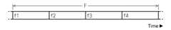
図3は、本実施形態におけるフレームとサブサブフレームとの関係を説明するための図である。この図に示されるように、本実施形態では、1つのフレームFが分割された4つのサブフレームには、符号として、時間の順にf1、f2、f3、f4が付与されている。
なお、フレームFの期間長は、同期信号Syncに含まれる垂直同期信号の周波数が60Hzである場合、1周期の16.7ミリ秒である。この場合、サブフレームf1~f4の期間長は、それぞれ4.17ミリ秒になる。 3 is a diagram for explaining the relationship between frames and sub-subframes in this embodiment. As shown in this diagram, in this embodiment, the four subframes into which one frame F is divided are assigned codes f1, f2, f3, and f4 in chronological order.
When the frequency of the vertical synchronizing signal included in the synchronizing signal Sync is 60 Hz, the period length of frame F is 16.7 milliseconds, which is one period. In this case, the period lengths of subframes f1 to f4 are each 4.17 milliseconds.
次に、映像データVid-inで階調レベルが指定される表示画素と、液晶パネル100によるパネル画素と、光学シフト素子230による投写位置と、の関係について説明する。なお、光学シフト素子230については、上述したようにダイクロイックプリズム2112からの投写方向をシフトさせるが、便宜的に当該シフト量については、スクリーンScrにおける投写画素(パネル画素)の大きさに換算する。
また、本実施形態では、RGBの三色のうち、相対的に視認性の高いGについては高解像度で表示され、相対的に視認性の低いRおよびBについては低解像度で表示される。 Next, a description will be given of the relationship between the display pixel whose gradation level is specified by the video data Vid-in, the panel pixel of the
In this embodiment, of the three colors RGB, G, which has relatively high visibility, is displayed at high resolution, and R and B, which have relatively low visibility, are displayed at low resolution.
図4における左欄は、映像データVid-inで示される表示画像のうち、一部だけを抜き出して示す図である。また、図4における右欄は、液晶パネル100のパネル画素のうち、当該左欄における表示画素の配列に対応した配列を抜き出して示す図である。The left column in FIG. 4 is a diagram showing only a portion of the display image shown by the video data Vid-in. The right column in FIG. 4 is a diagram showing an arrangement of the panel pixels of the
図4における映像データVid-inで示される表示画素の配列では、画素を区別するために、便宜的に符号として1行目にA1~A6が、2行目にB1~B6が、3行目にC1~C6が、4行目にD1~D6が、5行目にE1~E6が、6行目にF1~F6が、それぞれ付与されている。In the array of display pixels shown by the video data Vid-in in Figure 4, in order to distinguish between the pixels, the following symbols are conveniently assigned to the first row: A1 to A6, the second row: B1 to B6, the third row: C1 to C6, the fourth row: D1 to D6, the fifth row: E1 to E6, and the sixth row: F1 to F6.
図4におけるパネル画素の配列では、画素を区別するために、便宜的に符号として1行目にa1~a3が、2行目にb1~b3が、3行目にc1~c3が、それぞれ付与されている。
図4は、映像データの表示画素の配列では、太線枠で示される2×2の計4つの表示画素が1つのパネル画素で表現されることを示している。例えば、表示画素A1、A2、B2、B1の4つが、1つのパネル画素a1で表現される。また例えば、表示画素A3、A4、B4、B3の4つが、1つのパネル画素a2で表現される。 In the array of panel pixels in FIG. 4, for the sake of convenience, the first row is assigned the symbols a1 to a3, the second row b1 to b3, and the third row c1 to c3 to distinguish the pixels.
4 shows that in the arrangement of display pixels of video data, a total of four display pixels (2×2) indicated by a thick line frame are represented by one panel pixel. For example, the four display pixels A1, A2, B2, and B1 are represented by one panel pixel a1. Also, for example, the four display pixels A3, A4, B4, and B3 are represented by one panel pixel a2.
図5は、液晶プロジェクター1において、RGBの三色のうち、Gに対応する液晶パネル100Gのパネル画素が、映像データVid-inのうち、Gの表示画素を、どの投写位置で表示されるのかを示す図である。詳細には、図5は、図4のパネル画素が、図4の表示画素のうち、どの表示画素を、サブフレームf1~f4においてどの投写位置で表示するのかを示す図である。図5の1段目は、サブフレームf1で、例えば、パネル画素a1は表示画素A1に対応した情報を表示し、第1投写位置に投写することを示す。図5の2段目は、次に続くサブフレームf2で、例えば、パネル画素a1は、表示画素A2に対応した情報を表示し、第2投写位置に投写することを示す。図5の3段目は、次に続くサブフレームf?で、例えば、パネル画素a1は、表示画素B2に対応した情報を表示し、第3投写位置に投写することを示す。図5の4段目は、次に続くサブフレームf4で、例えば、パネル画素a1は、表示画素のB1に対応した情報を表示し、第4投写位置に投写することを示す。これにより、1つのフレームFで、パネル画素a1を用いて、表示画素A1、A2、B2、B1に基づく高解像の画像を表示できる。本実施形態では、表示画素A1、表示画素A2、表示画素B2および表示画素のB1は、それぞれ、第1表示画素、第2表示画素、第3表示画素および第4表示画素に対応する。また、サブフレームf1、サブフレームf2、サブフレームf?およびサブフレームf4は、それぞれ、第1期間、第2期間、第3期間および第4期間に対応する。また、第1投写位置、第2投写位置、第3投写位置および第4投写位置は、それぞれ、合成像の出射光路が第1位置、第2位置、第3位置および第4位置に対応した投写位置である。Figure 5 is a diagram showing at which projection position the panel pixel of the
便宜上、光学シフト素子230による投写位置を説明するために、フレームFの最初のサブフレームf1における投写位置を(A)とする。
サブフレームf1において、1つのパネル画素は、2×2の表示画素のうち、ハッチングが施された左上に位置する表示画素を表現する。詳細には、サブフレームf1において、パネル画素a1~a3、b1~b3、c1~c3は、順に表示画素A1、A3、A5、C1、C3、C5、E1、E3およびE5を表現する。ここで例えばパネル画素a1が表示画素A1を表現するとは、液晶パネル100Gのパネル画素a1は、映像データVid-inで示される表示画素A1のうち、G成分の階調レベルに相当する透過率となる、ということを意味である。 For convenience, in order to explain the projection position by the
In subframe f1, one panel pixel represents the hatched display pixel located at the upper left among the 2×2 display pixels. In detail, in subframe f1, panel pixels a1 to a3, b1 to b3, and c1 to c3 represent display pixels A1, A3, A5, C1, C3, C5, E1, E3, and E5, respectively. Here, for example, panel pixel a1 representing display pixel A1 means that panel pixel a1 of
次のサブフレームf2において、光学シフト素子230は、破線で示されるサブフレームf1の投写位置(A)から、図において右(Right)方向にパネル画素で0.5画素分シフトさせた投写位置(B)とする。
また、サブフレームf2において、1つのパネル画素は、2×2の表示画素のうち、ハッチングが施された右上に位置する表示画素を表現する。詳細には、サブフレームf2において、パネル画素a1~a3、b1~b3、c1~c3は、順に表示画素A2、A4、A6、C2、C4、C6、E2、E4およびE6を表現する。 In the next subframe f2, the
In subframe f2, one panel pixel represents the hatched display pixel located at the top right of the 2×2 display pixels. In detail, in subframe f2, panel pixels a1 to a3, b1 to b3, and c1 to c3 represent display pixels A2, A4, A6, C2, C4, C6, E2, E4, and E6, respectively.
サブフレームf3において、光学シフト素子230は、破線で示されるサブフレームf2での投写位置(B)から、図において下(Down)方向にパネル画素でみて0.5画素分シフトさせた投写位置(C)とする。
また、サブフレームf3において、1つのパネル画素は、2×2の表示画素のうち、ハッチングが施された右下に位置する表示画素を表現する。詳細には、サブフレームf3において、パネル画素a1~a3、b1~b3、c1~c3は、順に表示画素B2、B4、B6、D2、D4、D6、F2、F4およびF6を表現する。 In subframe f3, the
In subframe f3, one panel pixel represents the hatched display pixel located at the lower right among the 2×2 display pixels. In detail, in subframe f3, panel pixels a1 to a3, b1 to b3, and c1 to c3 represent display pixels B2, B4, B6, D2, D4, D6, F2, F4, and F6, respectively.
そして、サブフレームf4において、光学シフト素子230は、破線で示されるサブフレームf3での投写位置(C)から、図において左(Left)方向にパネル画素でみて0.5画素分シフトさせた投写位置(D)とする。
また、サブフレームf3において、1つのパネル画素は、2×2の表示画素のうち、ハッチングが施された左下に位置する表示画素を表現する。詳細には、サブフレームf4において、パネル画素a1~a3、b1~b3、c1~c3は、順に表示画素B1、B3、B5、D1、D3、D5、F1、F3およびF5を表現する。 In subframe f4, the
In subframe f3, one panel pixel represents the hatched lower left display pixel of the 2 × 2 display pixels. In detail, in subframe f4, panel pixels a1 to a3, b1 to b3, and c1 to c3 represent display pixels B1, B3, B5, D1, D3, D5, F1, F3, and F5, respectively.
サブフレームf4の後、光学シフト素子230は、破線で示されるサブフレームf4の投写位置(D)から、図において上(Up)方向にパネル画素でみて0.5画素分にシフトさせて投写位置(A)に戻す。After subframe f4, the
図6は、液晶プロジェクター1において、RGBの三色のうち、Rに対応する液晶パネル100Rのパネル画素が、映像データVid-inのうち、Rの成分の表示画素を、どの投写位置で表示されるのかを示す図である。
光学シフト素子230は、合成像の出射光路をシフトするので、投写位置は、RGB共通である。このため、サブフレームf1におけるRのパネル画素の投写位置は、Gと同様に投写位置(A)である。
図6の1段目は、第1期間(f1)で、例えば、パネル画素a1は、第1表示画素(A1)及び第2表示画素(A2)に対応した情報を表示し、第1投写位置(A)に投写することを示す。図6の2段目は、次に続く第2期間(f2)で、例えば、パネル画素a1は、第1表示画素(A1)及び第2表示画素(A2)に対応した情報を表示し、第2投写位置(B)に投写することを示す。図5の3段目は、次に続く第3期間(f?)で、例えば、パネル画素a1は、第3表示画素(B2)及び第4表示画素(B1)に対応した情報を表示し、第3投写位置(C)に投写することを示す。図5の4段目は、次に続く第4期間(f4)で、例えば、第1パネル画素a1は、第3表示画素(B2)及び第4表示画素(B1)に対応した情報を表示し、第4投写位置(D)に投写することを示す。これにより、1フレームで、パネル画素a1を用いて、第1表示画素A1および第2表示画素A2と、第3表示画素B2および第4表示画素B1により、上記の液晶パネル100Gでの表現よりは低下するが高解像の画像を表示できる。 Figure 6 is a diagram showing at what projection position in the
Since the
The first row of Fig. 6 shows that in a first period (f1), for example, the panel pixel a1 displays information corresponding to the first display pixel (A1) and the second display pixel (A2) and projects it to the first projection position (A). The second row of Fig. 6 shows that in a subsequent second period (f2), for example, the panel pixel a1 displays information corresponding to the first display pixel (A1) and the second display pixel (A2) and projects it to the second projection position (B). The third row of Fig. 5 shows that in a subsequent third period (f?), for example, the panel pixel a1 displays information corresponding to the third display pixel (B2) and the fourth display pixel (B1) and projects it to the third projection position (C). 5 shows that in the subsequent fourth period (f4), for example, the first panel pixel a1 displays information corresponding to the third display pixel (B2) and the fourth display pixel (B1) and projects it at the fourth projection position (D). As a result, in one frame, a high-resolution image can be displayed by the panel pixel a1 with the first display pixel A1 and the second display pixel A2, and the third display pixel B2 and the fourth display pixel B1, although the resolution is lower than that of the
図6に示すサブフレームf1において、Rの1つのパネル画素は、2×2の表示画素のうち、左上の表示画素におけるRの階調レベルおよび右上の表示画素におけるRの階調レベルの平均値を表現する。なお、2×2の表示画素のうち、左上の表示画素および右上の表示画素にはハッチングが施されている。階調レベルの平均値を表現するとは、当該階調レベルの平均値に相当する透過率とする、という意味である。
例えば、サブフレームf1において、Rのパネル画素a1は、表示画素A1におけるRの階調レベルおよび表示画素A2におけるRの階調レベルの平均値を表現する。図6のパネル画素においてパネル画素a1の「A1A2」は、表示画素A1の階調レベルおよび表示画素A2の階調レベルの平均値を表現することを意味する。
なお、図6のパネル画素においてパネル画素a2の「A3A4」についても、表示画素A3の階調レベルおよび表示画素A4の階調レベルの平均値を表現することを意味する。他のパネル画素についても同様である。 In subframe f1 shown in Fig. 6, one R panel pixel represents the average value of the R grayscale level in the upper left display pixel and the R grayscale level in the upper right display pixel among the 2 x 2 display pixels. Note that, among the 2 x 2 display pixels, the upper left display pixel and the upper right display pixel are hatched. Representing the average grayscale level means that the transmittance is set to be equivalent to the average grayscale level.
For example, in subframe f1, R panel pixel a1 represents the average value of the R gradation level in display pixel A1 and the R gradation level in display pixel A2. In the panel pixels of Figure 6, "A1A2" of panel pixel a1 represents the average value of the gradation level of display pixel A1 and the gradation level of display pixel A2.
6, "A3A4" of the panel pixel a2 also represents the average value of the grayscale level of the display pixel A3 and the grayscale level of the display pixel A4. The same is true for the other panel pixels.
サブフレームf2におけるRのパネル画素の投写位置は、Gと同様に投写位置(B)である。また、サブフレームf2において、Rの1つのパネル画素は、サブフレームf1から引き続き、2×2の表示画素のうち、左上の表示画素におけるRの階調レベルおよび右上の表示画素におけるRの階調レベルの平均値を表現する。このため、Rの1つのパネル画素は、サブフレームf1からサブフレームf2まで当該平均値に相当する透過率が継続する。The projection position of the R panel pixel in subframe f2 is projection position (B), just like G. Also, in subframe f2, the single R panel pixel continues from subframe f1 to represent the average value of the R gradation level of the top left display pixel and the R gradation level of the top right display pixel among the 2 x 2 display pixels. Therefore, the single R panel pixel continues to have a transmittance equivalent to this average value from subframe f1 to subframe f2.
サブフレームf3におけるRのパネル画素の投写位置は、Gと同様に投写位置(C)である。
サブフレームf3において、Rの1つのパネル画素は、2×2の表示画素のうち、右下の表示画素におけるRの階調レベルおよび左下の表示画素におけるRの階調レベルの平均値を表現する。
例えば、サブフレームf1において、Rのパネル画素a1は、表示画素B2におけるRの階調レベルおよび表示画素B1におけるRの階調レベルの平均値を表現する。 The projection position of the R panel pixel in subframe f3 is the projection position (C) just like G.
In subframe f3, one R panel pixel represents the average value of the R grayscale level of the lower right display pixel and the R grayscale level of the lower left display pixel among the 2×2 display pixels.
For example, in subframe f1, the R panel pixel a1 expresses the average value of the R grayscale level in the display pixel B2 and the R grayscale level in the display pixel B1.
サブフレームf4におけるRのパネル画素の投写位置は、Gと同様に投写位置(D)である。また、サブフレームf4において、Rの1つのパネル画素は、サブフレームf3から引き続き、2×2の表示画素のうち、右下の表示画素におけるRの階調レベルおよび左下の表示画素におけるRの階調レベルの平均値を表現する。
このため、Rの1つのパネル画素は、サブフレームf3からサブフレームf4まで当該平均値に相当する透過率が継続する。 The projection position of the R panel pixel in subframe f4 is projection position (D), similar to G. Furthermore, in subframe f4, one R panel pixel continues from subframe f3 to represent the average value of the R gradation level in the lower right display pixel and the R gradation level in the lower left display pixel among the 2×2 display pixels.
Therefore, one R panel pixel continues to have a transmittance equivalent to the average value from subframe f3 to subframe f4.
Bに対応する液晶パネル100Bのパネル画素が、映像データVid-inのうち、Bの成分の表示画素を、どの投写位置で表示されるのかについてもRと同様である。The panel pixels of the
再び説明を図2に戻すと、表示制御回路21は、液晶パネル100の走査をサブフレーム毎に制御するための制御信号Ctrを生成する。この制御信号Ctrには、液晶パネル100の走査線12の選択を制御するための制御信号や、データ線14にデータ信号を供給するための制御信号が含まれる。なお、本実施形態において制御信号Ctrは、液晶パネル100R、100Gおよび100Bに共通に供給される。
また、表示制御回路21は、サブフレーム毎に光学シフト素子230による投写位置を制御するための制御信号Lacを出力する。 2, the
In addition, the
なお、制御信号Lacには、スクリーンScrにおいて投写位置を上下にシフトさせる制御信号Lac_Yと、左右にシフトさせる制御信号Lac_Xとが含まれる。具体的には、光学シフト素子230による投写位置のうち、上または下方向が制御信号Lac_Yの電圧で指定され、左または右方向が制御信号Lac_Xの電圧で指定される。The control signal Lac includes a control signal Lac_Y that shifts the projection position on the screen Scr up and down, and a control signal Lac_X that shifts it left and right. Specifically, the upward or downward direction of the projection position by the
より具体的には、後述するが、光学シフト素子230は、制御信号Lac_Yの電圧が最高値であれば、投写位置を(A)または(B)とし、最低値であれば、投写位置を(C)または(D)とする。光学シフト素子230は、制御信号Lac_Yの電圧が最高値から最低値までであれば、当該電圧に応じて、投写位置(A)または(B)から投写位置(C)または(D)までの間の位置とさせる。More specifically, as described below, when the voltage of the control signal Lac_Y is at its highest value, the
また、光学シフト素子230は、制御信号Lac_Xの電圧が最高値であれば、投写位置を(A)または(D)とし、最低値であれば、投写位置を(B)または(C)とする。光学シフト素子230は、制御信号Lac_Xの電圧が最高値から最低値までであれば、当該電圧に応じて、投写位置(A)または(D)から投写位置(B)または(C)までの間の位置とさせる。In addition, the
映像処理回路22は、記憶装置221、処理装置222R、222Gおよび222Bを含む。
記憶装置221は、上位装置から供給された映像データVid-inを一旦蓄積する。
処理装置222Rは、記憶装置221に蓄積された映像データVid-inのうちRの映像データを読み出し、当該映像データのうち、2つの階調レベルを平均化し、当該平均化した階調レベルをアナログ信号に変換して、データ信号Vid-Rとして出力する。
処理装置222Bについても、処理装置222Rと同様に、記憶装置221に蓄積された映像データVid-inのうちBの映像データを読み出して、当該映像データのうち、2つの階調レベルを平均化し、当該平均化した階調レベルをアナログ信号に変換して、データ信号Vid-Bとして出力する。 The
The
The
As with the
なお、平均化の対象は、上述したように、サブフレームf1、f2では、2×2の表示画素のうち、左上および右上の表示画素の階調レベルであり、サブフレームf3、f4では、2×2の表示画素のうち、右下および左下の表示画素の階調レベルである。
また、サブフレームf1において、階調レベルを平均化したデータ信号Vid-R、Vid-Bを出力するには、平均化する時点で、サブフレームf2の映像データVid-inを取得できる状態でなければならない。このため、実際には、上位装置から、サブフレームf2に相当する映像データVid-inが記憶装置221に蓄積された時点以後に、処理装置222R、222Bが平均化を実行する。 As described above, the objects of averaging are the gradation levels of the top left and top right display pixels of the 2×2 display pixels in subframes f1 and f2, and the gradation levels of the bottom right and bottom left display pixels of the 2×2 display pixels in subframes f3 and f4.
Furthermore, in order to output data signals Vid-R and Vid-B with averaged gradation levels in subframe f1, the video data Vid-in of subframe f2 must be available at the time of averaging. Therefore, in practice, the
処理装置222Gは、記憶装置221に蓄積された映像データVid-inのうちGの映像データを読み出して、当該読み出した映像データの階調レベルをアナログ信号に変換して、データ信号Vid-Gとして出力する。
なお、処理装置222Gは、RBとは異なり、平均化処理を実行しないが、処理装置222Rによるデータ信号Vid-Rおよび処理装置222Bによるデータ信号Vid-Bに合わせたタイミングで、データ信号Vid-Gを出力する。 The
Unlike RB, the
次に、液晶パネル100R、100Gおよび100Gについて、色を特定しないで一般的な液晶パネル100として説明する。Next,
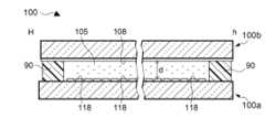
図7は、液晶パネル100の要部を示す図であり、図8は、図7におけるH-h線で破断した断面図である。
これらの図に示されるように、液晶パネル100は、画素電極118が設けられた素子基板100aと、コモン電極108が設けられた対向基板100bとが、図示省略のスペーサーを含むシール材90によって一定のセルギャップdを保ちつつ、互いに電極形成面が対向するように貼り合わせられ、当該セルギャップに液晶105が封入されている。 FIG. 7 is a diagram showing a main part of the
As shown in these figures, the
素子基板100aおよび対向基板100bとしては、それぞれガラスや石英などの光透過性を有する基板が用いられる。図7に示されるように、素子基板100aにおける一辺は、対向基板100bから張り出している。この張り出した領域に、当該一辺に沿って複数の端子106が設けられている。複数の端子106には、FPC基板の一端が接続される。FPC基板の他端は、制御回路20に接続されて、上述した各種の信号などが供給される。The
素子基板100aにおいて対向基板100bに向かう面には、画素電極118が、例えばITOなどの透明性を有する導電層のパターニングによって形成される。なお、ITOは、Indium Tin Oxideの略語である。また、素子基板100aの対向面および対向基板100bの対向面には、電極以外にも様々な要素が設けられるが、図では省略されている。On the surface of the
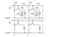
図9は、液晶パネル100の電気的な構成を示すブロック図である。液晶パネル100には、表示領域10の周縁に、走査線駆動回路130およびデータ線駆動回路140が設けられる。Figure 9 is a block diagram showing the electrical configuration of the
液晶パネル100の表示領域10においては、画素回路110がマトリクス状に配列する。詳細には、表示領域10において、複数本の走査線12が図において横方向に延在して設けられ、また、複数本のデータ線14が図において縦方向に延在し、かつ、走査線12と互いに電気的な絶縁を保って設けられる。そして、複数本の走査線12と複数本のデータ線14との交差に対応して画素回路110がマトリクス状に設けられる。In the
走査線12の本数をmとし、データ線14の本数をnとした場合、画素回路110は、上述したように、縦m行×横n列でマトリクス状に配列する。走査線12と画素回路110とにおいて、マトリクスの行を区別するために、図において上から順に1、2、3、…、m行と呼ぶ場合がある。同様にデータ線14および画素回路110において、マトリクスの列を区別するために、図において左から順に1、2、3、…、n列と呼ぶ場合がある。If the number of
走査線駆動回路130は、表示制御回路21による制御にしたがって、走査線12を例えば1、2、3、…、m行目という順番で1本ずつ選択し、選択した走査線12への走査信号をHレベルとする。なお、走査線駆動回路130は、選択した走査線12以外の走査線12への走査信号をLレベルとする。
データ線駆動回路140は、映像処理回路22から供給されたデータ信号を、表示制御回路21による制御にしたがって1行分ラッチし、走査線12への走査信号がHレベルとなった期間に当該走査線12に位置する画素回路110に、データ線14を介して出力する。 The scanning
The data line driving
図10は、隣り合う2本の走査線12と、隣り合う2本のデータ線14との交差に対応する2行2列の計4個の、画素回路110の等価回路を示す図である。
図に示されるように、画素回路110は、トランジスター116と液晶素子120とを含む。トランジスター116は、例えばnチャネル型の薄膜トランジスターである。画素回路110において、トランジスター116のゲートノードは、走査線12に接続される一方、そのソースノードはデータ線14に接続され、そのドレインノードは、平面視で略正方形の画素電極118に接続される。 FIG. 10 is a diagram showing an equivalent circuit of four
As shown in the figure, the
画素電極118に対向するようにコモン電極108が全画素回路に対して共通に設けられる。コモン電極108には電圧LCcomが印加される。そして、画素電極118とコモン電極108との間には液晶105が挟持される。したがって、画素回路110毎に、画素電極118およびコモン電極108によって液晶105を挟持した液晶素子120が構成される。
なお、液晶素子120に対して並列に蓄積容量が設けられることもあるが、本件では重要ではないので省略されている。 A
A storage capacitor may be provided in parallel with the
走査信号がHレベルとなった走査線12では、当該走査線12に対応して設けられる画素回路110のトランジスター116がオンする。トランジスター116のオンにより、データ線14と画素電極118とが電気的に接続された状態となるので、データ線14に供給されたデータ信号が、オンしたトランジスター116を介して画素電極118に到達する。走査線12がLレベルになると、トランジスター116はオフになるが、画素電極118に到達したデータ信号の電圧は、液晶素子120の容量性によって保持される。When the scanning signal for a
周知のように、液晶素子120では、画素電極118およびコモン電極108によって生じる電界に応じて液晶分子の配向が変化する。したがって、液晶素子120は、印加された電圧の実効値に応じた透過率となる。なお、本実施形態では、液晶素子120への印加電圧が高くなるにつれて、透過率が高くなるノーマリーブラックモードである。As is well known, in the
液晶素子120の画素電極118にデータ信号を供給する動作が、1サブフレームの期間において、1、2、3、…、m行目という順番で実行されることによって、m行n列で配列する画素回路110の液晶素子120の各々にデータ信号に応じた電圧が保持される。このような電圧の保持によって各液晶素子120が目的とする透過率となり、m行n列で配列する液晶素子120によって、対応する色の変調画像が生成される。The operation of supplying data signals to the
図11は、走査線12の選択推移の一例を示す図である。
走査線12の選択推移とは、走査線12の1行目からm行目までを縦軸にとり、経過時間を横軸とったときに、選択される走査線12が時間的にどうように移行するかを示すことである。走査線12が選択される状態を黒の太線で示したとき、走査線12はサブフレームf1~f4の各期間において1行ずつ排他的に選択される。この選択の順序は、上述したように1、2、3、…、m行目である。
あるサブフレームにおいて、ある走査線12が選択されたとき、あるデータ線14には、次のようなデータ信号が供給される。詳細には、あるデータ線14には、当該パネル画素に対応した4つの表示画素のうち、当該サブフレームに対応した表示画素の階調レベル、または、2つの階調レベルの平均値を変換したデータ信号が供給される。 FIG. 11 is a diagram showing an example of the selection transition of the scanning lines 12. In FIG.
The selection transition of the scanning lines 12 refers to how the selected
When a
なお、図11において、タイミングt10は、サブフレームf1の開始タイミングであり、詳細には、1~m行目のうち、先頭の1行目の走査線12への走査信号がHレベルとなるタイミングである。同様に、タイミングt12、t14およびt16は、この順でサブフレームf2、f3およびf4の開始タイミングである。
また、タイミングt20は、サブフレームf1において、1~m行目のうち、中間の(m/2)行目の走査線12への走査信号がHレベルとなるタイミングである。同様に、タイミングt22、t24およびt26は、この順でサブフレームf2、f3およびf4において、(m/2)行目の走査線12への走査信号がHレベルとなるタイミングである。 11, timing t10 is the start timing of subframe f1, more specifically, the timing when the scanning signal to scanning
Furthermore, timing t20 is the timing at which the scanning signal to the
図12は、サブフレームf1~f4における映像処理回路22の動作を示すフローチャートである。Figure 12 is a flowchart showing the operation of the
ここで、映像データVid-inに示される画像の2×2の表示画素を便宜的に1つのブロックとする。ブロックはパネル画素と同じm行n列で配列する。このため、ブロックとパネル画素とは一対一に対応し、ある1つのパネル画素は、当該パネル画素に対応するブロックの2×2の表示画素を、サブフレームf1~f4で順番に投写位置をシフトしながら表現する。ブロックの2×2の表示画素は、例えば、左上、右上、右下、および左下の4つの表示画素である。
以下のサブフレームf1~f4における処理については、1つのブロックについて説明するが、実際には、m行n列で配列するブロックの各々について実行される。 Here, for the sake of convenience, 2×2 display pixels of an image shown in the video data Vid-in are considered to be one block. The blocks are arranged in the same m rows and n columns as the panel pixels. Therefore, there is a one-to-one correspondence between the blocks and the panel pixels, and a given panel pixel represents the 2×2 display pixels of the block corresponding to that panel pixel by shifting the projection position in turn in the subframes f1 to f4. The 2×2 display pixels of the block are, for example, the four display pixels at the top left, top right, bottom right, and bottom left.
Although the following processing in subframes f1 to f4 will be described for one block, in reality, the processing is carried out for each of the blocks arranged in m rows and n columns.
まず、映像処理回路22は、液晶パネル100R、100Gおよび100Bの駆動タイミングが、サブフレームf1の開始タイミングであるか否かを判定する(ステップS11)。なお、液晶パネル100R、100G、100Bと光学シフト素子230とは、表示制御回路21によって制御される。このため、映像処理回路22は、表示制御回路21の制御によって、サブフレームf1の開始タイミングであるか否か判定することができる。First, the
駆動タイミングがサブフレームf1の開始タイミングでなければ(ステップS11の判定結果が「No」であれば)、映像処理回路22は処理手順をステップS11に戻す。したがって、駆動タイミングがサブフレームf1の開始タイミングに至るまで、映像処理回路22は待機状態となる。If the drive timing is not the start timing of subframe f1 (if the determination result of step S11 is "No"), the
駆動タイミングがサブフレームf1の開始タイミングになれば(ステップS11の判定結果が「Yes」になれば)、映像処理回路22は、次のようなデータ信号Vid-R、Vid-G、Vid-Bを出力する(ステップS12)。
詳細には、映像処理回路22は、Gについて2×2の表示画素(1ブロック)のうち、左上の表示画素の映像データVid-inを記憶装置221から読み出して、当該映像データで指定される階調レベルをアナログ信号に変換し、データ信号Vid-Gとして液晶パネル100Gに供給する。 When the drive timing reaches the start timing of subframe f1 (when the determination result in step S11 is "Yes"), the
In detail, the
また、映像処理回路22は、Rについて1ブロックのうち、左上の表示画素の映像データVid-inおよび右上の表示画素の映像データVid-inを記憶装置221から読み出し、当該2つの映像データで指定される階調レベルの平均値を算出し、当該階調レベルの平均値をアナログ信号に変換し、データ信号Vid-Rとして液晶パネル100Rに供給する。
映像処理回路22は、Bについても同様に1ブロックのうち、左上の表示画素の階調レベルおよび右上の表示画素の階調レベルの平均値を算出し、当該階調レベルの平均値をアナログ信号に変換し、データ信号Vid-Bとして液晶パネル100Bに供給する。
サブフレームf1では、このような動作が1行目からm行目までの各ブロックについて順番に実行される。この後、映像処理回路22は、処理手順を、ステップS13に移行させる。 In addition, the
Similarly, for B, the
In subframe f1, such an operation is executed in order for each block from
映像処理回路22は、液晶パネル100R、100Gおよび100Bの駆動タイミングが、サブフレームf2の開始タイミングであるか否かを判定する(ステップS13)。駆動タイミングがサブフレームf2の開始タイミングに至れば(ステップS13の判定結果が「Yes」になれば)、映像処理回路22は、次のようなデータ信号Vid-R、Vid-G、Vid-Bを出力する(ステップS14)。The
詳細には、映像処理回路22は、Gについて1ブロックのうち、右上の表示画素の映像データVid-inで指定される階調レベルをアナログ信号に変換して、データ信号Vid-Gとして液晶パネル100Gに供給する。
また、映像処理回路22は、Rについて1ブロックのうち、左上の表示画素の階調レベルおよび右上の表示画素の階調レベルの平均値を、アナログ信号に変換して、データ信号Vid-Rとして液晶パネル100Rに供給する。このため、同じブロックおよびパネル画素で比較したとき、サブフレームf1およびf2におけるデータ信号Vid-Rは同一である。
映像処理回路22は、Bについても同様に、1ブロックのうち、左上の表示画素の階調レベルおよび右上の表示画素の階調レベルの平均値を、アナログ信号に変換して、データ信号Vid-Bとして液晶パネル100Bに供給する。このため、同じブロックおよびパネル画素で比較したとき、サブフレームf1およびf2におけるデータ信号Vid-Bは同一である。
サブフレームf2では、このような動作が1行目からm行目までの各ブロックについて順番に実行される。この後、映像処理回路22は、処理手順を、ステップS15に移行させる。 In detail, the
Furthermore, the
Similarly, for B, the
In subframe f2, such an operation is executed in order for each block from
映像処理回路22は、液晶パネル100R、100Gおよび100Bの駆動タイミングが、サブフレームf3の開始タイミングであるか否かを判定する(ステップS15)。駆動タイミングがサブフレームf3の開始タイミングに至れば(ステップS15の判定結果が「Yes」になれば)、映像処理回路22は、次のようなデータ信号Vid-R、Vid-G、Vid-Bを出力する(ステップS16)。The
詳細には、映像処理回路22は、Gについて1ブロックのうち、右下の表示画素の映像データVid-inで指定される階調レベルをアナログ信号に変換して、データ信号Vid-Gとして液晶パネル100Gに供給する。
また、映像処理回路22は、Rについて1ブロックのうち、右下の表示画素の階調レベルおよび左下の表示画素の階調レベルの平均値を、アナログ信号に変換して、データ信号Vid-Rとして液晶パネル100Rに供給する。
映像処理回路22は、Bについても同様に、1ブロックのうち、右下の表示画素の階調レベルおよび左下の表示画素の階調レベルの平均値を、アナログ信号に変換して、データ信号Vid-Bとして液晶パネル100Bに供給する。
サブフレームf3では、このような動作が1行目からm行目までの各ブロックについて順番に実行される。この後、映像処理回路22は、処理手順を、ステップS17に移行させる。 In detail, the
Furthermore, the
Similarly, for B, the
In subframe f3, such an operation is executed in order for each block from
映像処理回路22は、液晶パネル100R、100Gおよび100Bの駆動タイミングが、サブフレームf4の開始タイミングであるか否かを判定する(ステップS17)。駆動タイミングがサブフレームf4の開始タイミングに至れば(ステップS17の判定結果が「Yes」になれば)、映像処理回路22は、次のようなデータ信号Vid-R、Vid-G、Vid-Bを出力する(ステップS18)。The
詳細には、映像処理回路22は、Gについて1ブロックのうち、左下の表示画素の映像データVid-inで指定される階調レベルをアナログ信号に変換して、データ信号Vid-Gとして液晶パネル100Gに供給する。
また、映像処理回路22は、Rについて1ブロックのうち、右下の表示画素の階調レベルおよび左下の表示画素の階調レベルの平均値を、アナログ信号に変換して、データ信号Vid-Rとして液晶パネル100Rに供給する。このため、同じブロックおよびパネル画素で比較したとき、サブフレームf3およびf4におけるデータ信号Vid-Rは同一である。
映像処理回路22は、Bについても同様に、1ブロックのうち、右下の表示画素の階調レベルおよび左下の表示画素の階調レベルの平均値を、アナログ信号に変換して、データ信号Vid-Bとして液晶パネル100Bに供給する。このため、同じブロックおよびパネル画素で比較したとき、サブフレームf3およびf4におけるデータ信号Vid-Bは同一である。
サブフレームf4では、このような動作が1行目からm行目までの各ブロックについて順番に実行される。この後、映像処理回路22は、処理手順を、ステップS11に戻して、次のフレームに備える。
なお、このようなステップS11~S18の動作は電源が遮断されるまで、あるいは、上位装置からの映像データVid-inの供給が途絶えるまで、繰り返し実行される。 In detail, the
Furthermore, the
Similarly, for B, the
In subframe f4, such an operation is executed in order for each block from
The operations of steps S11 to S18 are repeatedly executed until the power supply is cut off or the supply of video data Vid-in from the higher-level device is cut off.
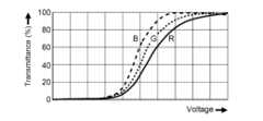
図13は、液晶パネル100Gにおける液晶素子120の光学応答と、液晶パネル100R(または100B)における液晶素子の光学応答との関係等を示す図である。
なお、光学応答とは、液晶素子120に電圧が印加されてからの透過率の変化を意味する。 FIG. 13 is a diagram showing the relationship between the optical response of the
The optical response refers to the change in transmittance after a voltage is applied to the
この例は、1ブロックのうち、左上および右下の表示画素の階調レベルがRGBにおいて最高値であり、右上および左下の表示画素の階調レベルがRGBにおいて最低値が指定されている場合を示している。また、この例では、液晶素子120が、中間の(m/2)行に位置する場合を想定している。This example shows a case where the gradation levels of the upper left and lower right display pixels in one block are the highest RGB values, and the gradation levels of the upper right and lower left display pixels are the lowest RGB values. This example also assumes that the
この例において、Gの液晶素子120における透過率は、タイミングt20からタイミングt22まで100%となり、タイミングt22からタイミングt24まで0%となり、タイミングt24からタイミングt26まで100%となり、タイミングt22からタイミングt28まで0%となるのが理想的である。なお、ここでいう透過率とは、最低値を0%とし、最高値を100%として正規化した相対透過率である。
このため、Gの液晶素子120の光学応答は、1つのサブフレーム毎に、表示画素の階調レベルの変化に応じて変化することが要求される。すなわち、液晶パネル100Gでは、高解像の表現のためには、比較的速い光学応答が要求される。
なお、Gの液晶素子120の光学応答は、実際には図に示されるように時間的な遅れを伴って変化する。 In this example, ideally, the transmittance of the G
For this reason, the optical response of the G
In reality, the optical response of the G
一方、RおよびBでは、サブフレームf1およびf2において、1ブロックのうち、左上および右下の表示画素の階調レベルの平均値が指定される。このため、R、Bの液晶素子120における透過率は、タイミングt20からタイミングt24まで50%となるのが理想的である。
また、RおよびBでは、サブフレームf3およびf4において、1ブロックのうち、右下および左上の表示画素の階調レベルの平均値が指定される。このため、R、Bの液晶素子120における透過率は、タイミングt24からタイミングt28まで50%となるのが理想的である。
このため、R、Bの液晶素子120の光学応答は、2つサブフレーム毎に、表示画素の階調レベルの変化に応じて変化すればよいので、液晶パネル100Rおよび100Bでは、液晶パネル100Gと比較して速い光学応答が要求されない、すなわち、光学応答は遅くで済む。 On the other hand, the average values of the gradation levels of the upper left and lower right display pixels in one block are specified in subframes f1 and f2 for R and B. Therefore, it is ideal that the transmittance of the R and B
Furthermore, the average values of the gradation levels of the lower right and upper left display pixels in one block are specified in subframes f3 and f4 for R and B. Therefore, it is ideal that the transmittance of the R and B
For this reason, the optical response of the R and B
図13は、セルギャップが狭い場合において、液晶素子120への印加電圧に対する透過率の特性例を示す図である。また、図14は、セルギャップが広い場合において、液晶素子120への印加電圧に対する透過率の特性例を示す図である。Figure 13 is a diagram showing an example of the characteristics of the transmittance versus the voltage applied to the
図13および図14に示されるように、液晶素子120への印加電圧が同じであっても、入射光の波長(色)が異なれば透過率が異なる。具体的には、液晶素子120への印加電圧が同じあれば、入射光の波長が短くなるにつれて、透過率が高くなる傾向があり、透過率について波長依存性がある。この波長依存性は、セルギャップが狭くても、広くても同様に現れる。
次に、セルギャップが狭い場合と広い場合とでは、液晶素子120への印加電圧が同じであれば、透過率はセルギャップが広い場合の方が高くなる傾向がある。換言すれば、セルギャップを狭い場合、印加電圧が同じであれば、得られる透過率が低くなり、明るさが低下する傾向がある。 13 and 14, even if the voltage applied to the
Next, when the cell gap is narrow and when the cell gap is wide, if the same voltage is applied to the
液晶パネル100の光学応答を速くするためには、温度を高くすることや、セルギャップを狭くする等が必要となるが、上述したように、図13および図14に示されるように、セルギャップを狭くすると、高い透過率が得られにくくなり、明るさが低下する。
本実施形態によれば、液晶パネル100Rおよび100Bでは、光学応答が遅くて済むので、当該液晶パネル100Rおよび100Bのセルギャップを、液晶パネル100Gのセルギャップよりも広くすることができる。
換言すれば、液晶パネル100Rおよび100Bの光学応答が遅くて済むので、当該液晶パネル100Rおよび100Bのセルギャップを狭くする構成や、当該液晶パネル100Rおよび100Bの温度を高くするための構成が必要でない。また、液晶パネル100Rおよび100Bの明るさ低下させる構成とする必要でない。当該液晶パネル100Rおよび100Bは、特殊な構成とする必要でないので、コストを抑制できる。 In order to speed up the optical response of the
According to this embodiment, since the
In other words, since the optical response of the
図15には、光学シフト素子230による投写位置と、制御信号Lac_Y、Lac_Xとの関係についても示されている。
詳細には、制御信号Lac_Yの電圧は、タイミングt20からt21までの期間において最低値から最高値まで上昇し、タイミングt24まで最高値を維持し、タイミングt24からt26までの期間において最高値から最低値まで低下し、次のフレームのタイミングt20まで最低値を維持する。
また、制御信号Lac_Xの電圧は、タイミングt22からt23までの期間で最高値から最低値まで低下し、タイミングt26まで最低値を維持し、タイミングt26からt27までの期間で最低値から最高値まで上昇し、次フレームのタイミングt22まで最高値を維持する。
このように制御信号Lac_Y、Lac_Xの電圧となっている理由について説明する。 FIG. 15 also shows the relationship between the projection position by the
In detail, the voltage of the control signal Lac_Y rises from the lowest value to the highest value in the period from timing t20 to t21, maintains the highest value until timing t24, falls from the highest value to the lowest value in the period from timing t24 to t26, and maintains the lowest value until timing t20 of the next frame.
In addition, the voltage of the control signal Lac_X decreases from the highest value to the lowest value in the period from timing t22 to t23, maintains the lowest value until timing t26, increases from the lowest value to the highest value in the period from timing t26 to t27, and maintains the highest value until timing t22 of the next frame.
The reason why the control signals Lac_Y and Lac_X have such voltages will be described.
液晶素子120の画素電極118にデータ信号の電圧が印加されるタイミングは、図11に示されるように、当該液晶素子120に対応する走査線12の行が小さいほど早く、行が大きいほど遅い。第1行から第m行に向かって走査が行われるため、すべての液晶素子120を同じ透過率に書き換える場合であっても、各行において透過率が異なる状況が発生する。
これに対して、光学シフト素子230は、合成像の出射光路をシフトするため、各行におけるシフトは共通である。 11, the timing at which a data signal voltage is applied to the
In contrast, the
このため、光学シフト素子230は、例えば中間の(m/2)行目における実際のGの透過率が目的とする値に近くなる期間で、当該サブフレームの投写位置となるように制御され、他の期間では、投写位置を移動するように制御される。
詳細には、例えばサブフレームf1において、(m/2)行目のGの液晶素子120における実際の透過率が目的の透過率と同視できる値となるタイミングt21からt22までの期間で、光学シフト素子230は、投写位置(A)に固定されるように制御される。 同様にして、光学シフト素子230は、サブフレームf2では、タイミングt23からt24までの期間で投写位置(B)に固定されるように制御され、サブフレームf3では、タイミングt25からt26までの期間で投写位置(C)に固定されるように制御され、サブフレームf4では、タイミングt27からt28(次のフレームのタイミングt20)までの期間で投写位置(D)に固定されるように制御される。 For this reason, the
In detail, for example, in subframe f1, the
また、タイミングt22からt23までは、光学シフト素子230は、投写位置(A)から投写位置(B)までシフトするように制御される。同様に、光学シフト素子230は、タイミングt24からt25までは投写位置(B)から投写位置(C)までシフトするように制御され、タイミングt26からt27までは投写位置(C)から投写位置(D)までシフトするように制御され、タイミングt28から次のフレームにおけるタイミングt21までは投写位置(D)から投写位置(A)までシフトするように制御される。In addition, from timing t22 to t23, the
なお、中間の(m/2)行目におけるGの液晶素子120の透過率が目的値となるように、光学シフト素子230の投写位置を制御する場合、他の行については、特に1行目とm行目とについては、目的値から乖離した透過率の状態で投写位置が固定されるが、表示領域10の中心から離れているので、表示品位の低下として視認されにくい。When controlling the projection position of the
実施形態に係る液晶プロジェクター1では、実施形態に限られるものではなく、以下に述べる各種の変形が可能である。また、実施形態および各変形例を適宜組み合わせてもよい。The
実施形態では、RBについて、サブフレームf1およびf2と、サブフレームf3およびf4とで階調レベルの平均値を算出する構成としたが、サブフレームf1~f4の階調レベルの平均値を算出する構成としてもよい。また、平均化に限られず、例えば、階調レベルの変化を滑らかにするローパスフィルターを介して出力された階調レベルをアナログのデータ信号に変換して出力する構成としてもよい。
すなわち、複数の連続するサブフレームの期間でみたときに、液晶パネル100R、100Bで表現される変調画像の解像度を、液晶パネル100Gで表現される変調画像の解像度よりも低下させることによって、液晶パネル100R、100Bの光学応答を、液晶パネル100Gの光学応答よりも遅くすればよい。 In the embodiment, the average value of the gradation levels of subframes f1 and f2 and subframes f3 and f4 for RB is calculated, but the average value of the gradation levels of subframes f1 to f4 may be calculated. Also, without being limited to averaging, for example, the gradation levels output through a low-pass filter that smooths the change in gradation level may be converted into an analog data signal and output.
In other words, when viewed over a period of multiple consecutive subframes, the resolution of the modulated image displayed by
実施形態では、ノーマリーブラックモードで説明したが、ノーマリーホワイトモードとしてもよい。また、液晶パネル100R、100G、100Bを透過型としたが、反射型としてもよい。液晶パネル100R、100G、100Bを反射型とする場合、上述した説明において、透過率を反射率に読み替えればよい。In the embodiment, the normally black mode has been described, but the normally white mode may also be used. Also, the
実施形態において、光学シフト素子230は、投写面に上下方向および左右方向の2軸でシフトする構成としたが、例えば上下方向、左右方向または斜め方向の1軸でシフトする構成としてもよい。In the embodiment, the
以上に説明した実施形態および変形例(以下、実施形態等と表記する)から、例えば以下の態様が把握される。The embodiments and variations (hereinafter referred to as "embodiments") described above give rise to the following aspects, for example:
ひとつの態様(態様1)に係る液晶プロジェクターは、第1色光の第1変調画像を生成する第1液晶パネルと、前記第1色光の波長よりも短い第2色光の第2変調画像を生成する第2液晶パネルと、前記第2色光の波長よりも短い第3色光の第3変調画像を生成する第3液晶パネルと、を含み、前記第1変調画像、前記第2変調画像および前記第3変調画像を合成する合成部と、前記合成部による合成像の出射光路をシフトさせる光学シフト素子と、前記第1液晶パネル、前記第2液晶パネル、前記第3液晶パネルおよび前記光学シフト素子を制御する制御回路と、を含み、前記制御回路は、前記光学シフト素子を制御して、前記出射光路を、第1期間で第1位置にシフトさせ、前記第1期間の後の第2期間で第2位置にシフトさせ、前記第1液晶パネル、前記第2液晶パネルおよび前記第3液晶パネルを制御して、前記第1期間および前記第2期間で表現される前記第1変調画像または前記第3変調画像の少なくとも一方の解像度を、前記第1期間および前記第2期間で表現される前記第2変調画像の解像度よりも低下させる。
この態様によれば、第1液晶パネルまたは第3液晶パネルに要求される光学応答が、第2液晶パネルに要求される光学応答よりも緩和されるので、第1液晶パネルまたは第3液晶パネルによる表示画像の明るさの低下を抑えることができる。なお、第1色光および第3色光の視認性は、第2色光の視認性よりも劣るので、第1色光および第3色光の画像の解像度が、第2色光の画像の解像度よりも低下しても、3色の変調画像の合成像の解像度に与える影響は少ない。よって、第1液晶パネル、第2液晶パネルおよび第3液晶パネルにより、高解像で明るい表示画像を表現することができる。
なお、赤色光が第1色光の一例であり、緑色光が第2色光の一例であり、青色光が第3色光の一例である。また、液晶パネル100Rが第1液晶パネルの一例であり、液晶パネル100Gが第2液晶パネルの一例であり、液晶パネル100Bが第3液晶パネルの一例である。例えば光学シフト素子230によって投写画素を投写位置(A)とさせる出射光路の位置が第1位置の例であり、投写画素を投写位置(B)とさせる出射光路の位置が第2位置の例である。 A liquid crystal projector according to one aspect (aspect 1) includes a first liquid crystal panel that generates a first modulated image of a first color light, a second liquid crystal panel that generates a second modulated image of a second color light having a wavelength shorter than that of the first color light, and a third liquid crystal panel that generates a third modulated image of a third color light having a wavelength shorter than that of the second color light, and includes a combination unit that combines the first modulated image, the second modulated image, and the third modulated image, an optical shift element that shifts an output optical path of a combined image by the combination unit, and a control circuit that controls the first liquid crystal panel, the second liquid crystal panel, the third liquid crystal panel, and the optical shift element, and the control circuit controls the optical shift element to shift the output optical path to a first position in a first period and to a second position in a second period after the first period, and controls the first liquid crystal panel, the second liquid crystal panel, and the third liquid crystal panel to reduce the resolution of at least one of the first modulated image or the third modulated image displayed in the first period and the second period to be lower than the resolution of the second modulated image displayed in the first period and the second period.
According to this aspect, the optical response required for the first or third liquid crystal panel is less stringent than that required for the second liquid crystal panel, so that the decrease in brightness of the display image by the first or third liquid crystal panel can be suppressed. Note that since the visibility of the first and third color lights is inferior to that of the second color light, even if the resolution of the image of the first and third color lights is lower than that of the image of the second color light, the effect on the resolution of the composite image of the three color modulated images is small. Therefore, the first, second, and third liquid crystal panels can display a high-resolution and bright display image.
The red light is an example of the first color light, the green light is an example of the second color light, and the blue light is an example of the third color light. The
態様1の具体的な態様(態様2)において、前記制御回路は、前記第1期間および前記第2期間で表現される前記第1変調画像の解像度、および、前記第1期間および前記第2期間で表現される前記第3変調画像の解像度を、前記第1期間および前記第2期間で表現される前記第2変調画像の解像度よりも低下させる。
この態様によれば、第1液晶パネルおよび第3液晶パネルの双方による表示画像の明るさの低下を抑えることができる。 In a specific aspect (aspect 2) of
According to this aspect, it is possible to suppress a decrease in brightness of images displayed by both the first liquid crystal panel and the third liquid crystal panel.
態様2の具体的な態様(態様3)に係る液晶プロジェクターにおいて、前記制御回路は、前記第1液晶パネルにおける一のパネル画素を、前記第1期間および前記第2期間で、映像データで指定される第1表示画素の階調レベルのうち前記第1色光の階調レベルと第2表示画素のうち前記第1色光の階調レベルとを処理したレベルに基づいた階調とし、前記第2液晶パネルにおける前記一のパネル画素を、前記第1期間で、前記第1表示画素の階調レベルのうち前記第2色光の階調レベルに基づいた階調とし、前記第2期間で、前記第2表示画素の階調レベルのうち前記第2色光の階調レベルに基づいた階調とし、前記第1期間および前記第2期間で、前記第1表示画素の階調レベルのうち前記第3色光の階調レベルと前記第2表示画素のうち前記第3色光の階調レベルとを処理したレベルに基づいた階調とする。
この態様によれば、第1液晶パネルは第1期間および第2期間で同じ階調、詳細には、第1表示画素における第1色光の階調レベルと第2表示画素における第1色光の階調レベルとを処理したレベルに基づいた階調、となる。第3液晶パネルについても同様に第1期間および第2期間で同じ階調となる。このため、第1液晶パネルおよび第3液晶パネルは、第1期間および第2期間で同じ階調を表示すれば済む。 In a liquid crystal projector according to a specific aspect (aspect 3) of
According to this aspect, the first liquid crystal panel has the same gradation in the first period and the second period, specifically, a gradation based on a level obtained by processing the gradation level of the first color light in the first display pixel and the gradation level of the first color light in the second display pixel. Similarly, the third liquid crystal panel has the same gradation in the first period and the second period. Therefore, it is only necessary for the first liquid crystal panel and the third liquid crystal panel to display the same gradation in the first period and the second period.
態様3の具体的な態様(態様4)に係る液晶プロジェクターにおいて、前記処理は、前記第1期間における階調レベルおよび前記第2期間における階調レベルの平均化処理、変換処理、または、フィルタリング処理である。
なお、変換処理とは、例えば第1期間における階調レベルおよび第2期間における階調レベルを、ルックアップテーブルを参照して求めた階調レベルなどをいい、また、フィルタリング処理とは、例えば第1期間における階調レベルから第2期間における階調レベルへの変化をローパスフィルターで鈍化させることによって得られる階調レベルをいう。 In a liquid crystal projector according to a specific aspect (aspect 4) of
The conversion process refers to, for example, a gradation level in the first period and a gradation level in the second period that are determined by referring to a lookup table, and the filtering process refers to, for example, a gradation level that is obtained by slowing down the change from the gradation level in the first period to the gradation level in the second period using a low-pass filter.
態様4の具体的な態様(態様5)に係る液晶プロジェクターにおいて、前記制御回路は、前記光学シフト素子を制御して、前記出射光路を、前記第2期間の後に第3位置にシフトさせ、前記第3期間の後の第4期間で第4位置にシフトさせ、前記第3期間および前記第4期間で表現される前記第1変調画像または前記第3変調画像の少なくとも一方の解像度を、前記第3期間および前記第4期間で表現される前記第2変調画像の解像度よりも低下させる。
この態様によれば、合成像の出射光路が第1位置乃至第4位置にシフトされるので、解像度を第1態様よりも高めることができる。 In a liquid crystal projector according to a specific aspect (aspect 5) of aspect 4, the control circuit controls the optical shift element to shift the output light path to a third position after the second period, and to a fourth position in a fourth period after the third period, thereby reducing the resolution of at least one of the first modulated image or the third modulated image represented in the third period and the fourth period below the resolution of the second modulated image represented in the third period and the fourth period.
According to this aspect, since the emission optical path of the composite image is shifted to any one of the first position to the fourth position, the resolution can be increased more than that of the first aspect.
なお、態様1乃至態様5については、液晶プロジェクターの制御方法として表現することも可能である。Note that
1…液晶プロジェクター、20…制御回路、21…走査制御回路、22…映像処理回路、100、100R、100G、100B…液晶パネル、110…画素回路、120…液晶素子、230…光学シフト素子。1: Liquid crystal projector, 20: Control circuit, 21: Scanning control circuit, 22: Image processing circuit, 100, 100R, 100G, 100B: Liquid crystal panel, 110: Pixel circuit, 120: Liquid crystal element, 230: Optical shift element.
Claims (8)
Translated fromJapanese前記第1色光の波長よりも短い第2色光の第2変調画像を生成する第2液晶パネルと、
前記第2色光の波長よりも短い第3色光の第3変調画像を生成する第3液晶パネルと、
を含み、前記第1変調画像、前記第2変調画像および前記第3変調画像を合成する合成部と、
前記合成部による合成像の出射光路をシフトさせる光学シフト素子と、
前記第1液晶パネル、前記第2液晶パネル、前記第3液晶パネルおよび前記光学シフト素子を制御する制御回路と、
を含み、
前記制御回路は、
前記光学シフト素子を制御して、前記出射光路を、第1期間で第1位置にシフトさせ、前記第1期間の後の第2期間で第2位置にシフトさせ、
前記第1液晶パネル、前記第2液晶パネルおよび前記第3液晶パネルを制御して、前記第1期間および前記第2期間で表現される前記第1変調画像または前記第3変調画像の少なくとも一方の解像度を、前記第1期間および前記第2期間で表現される前記第2変調画像の解像度よりも低下させる、
液晶プロジェクター。
a first liquid crystal panel for generating a first modulated image of a first color light;
a second liquid crystal panel for generating a second modulated image of a second color light having a wavelength shorter than that of the first color light;
a third liquid crystal panel for generating a third modulated image of a third color light having a wavelength shorter than that of the second color light;
a synthesis unit that synthesizes the first modulated image, the second modulated image, and the third modulated image;
an optical shift element that shifts an output optical path of the composite image by the composition unit;
a control circuit for controlling the first liquid crystal panel, the second liquid crystal panel, the third liquid crystal panel, and the pixel shift element;
Including,
The control circuit includes:
controlling the optical shift element to shift the output optical path to a first position in a first period and to a second position in a second period after the first period;
controlling the first liquid crystal panel, the second liquid crystal panel, and the third liquid crystal panel to reduce a resolution of at least one of the first modulated image and the third modulated image displayed in the first period and the second period to be lower than a resolution of the second modulated image displayed in the first period and the second period;
LCD projector.
前記第1期間および前記第2期間で表現される前記第1変調画像の解像度、および、前記第1期間および前記第2期間で表現される前記第3変調画像の解像度を、
前記第1期間および前記第2期間で表現される前記第2変調画像の解像度よりも低下させる、
請求項1に記載の液晶プロジェクター。
The control circuit includes:
A resolution of the first modulated image expressed in the first period and the second period, and a resolution of the third modulated image expressed in the first period and the second period,
a resolution of the second modulated image is reduced to a level lower than that of the second modulated image expressed in the first period and the second period;
2. The liquid crystal projector according to claim 1.
前記第1液晶パネルにおける一のパネル画素を、
前記第1期間および前記第2期間で、映像データで指定される第1表示画素の階調レベルのうち前記第1色光の階調レベルと第2表示画素のうち前記第1色光の階調レベルとを平均化した階調とし、
前記第2液晶パネルにおける前記一のパネル画素を、
前記第1期間で、前記第1表示画素の階調レベルのうち前記第2色光の階調レベルに基づいた階調とし、前記第2期間で、前記第2表示画素の階調レベルのうち前記第2色光の階調レベルに基づいた階調とし、
前記第3液晶パネルにおける前記一のパネル画素を、
前記第1期間および前記第2期間で、前記第1表示画素の階調レベルのうち前記第3色光の階調レベルと前記第2表示画素のうち前記第3色光の階調レベルとを平均化した階調とする、
請求項2に記載の液晶プロジェクター。
The control circuit includes:
A panel pixel in the first liquid crystal panel is
a grayscale level of the first color light among grayscale levels of the first display pixel and a grayscale level of the first color light among grayscale levels of the second display pixel specified by video data during the first period and the second period is set as an average grayscale level;
The one panel pixel in the second liquid crystal panel,
a grayscale level based on the grayscale level of the second color light among the grayscale levels of the first display pixel during the first period, and a grayscale level based on the grayscale level of the second color light among the grayscale levels of the second display pixel during the second period;
The one panel pixel in the third liquid crystal panel,
a grayscale level of the third color light among the grayscale levels of the first display pixel and a grayscale level of the third color light among the grayscale levels of the second display pixel are averaged during the first period and the second period.
3. The liquid crystal projector according to claim 2.
前記光学シフト素子を制御して、前記出射光路を、
前記第2期間の後の第3期間で第3位置にシフトさせ、前記第3期間の後の第4期間で第4位置にシフトさせ、
前記第3期間および前記第4期間で表現される前記第1変調画像または前記第3変調画像の少なくとも一方の解像度を、前記第3期間および前記第4期間で表現される前記第2変調画像の解像度よりも低下させる、
請求項1に記載の液晶プロジェクター。
The control circuit includes:
The optical shift element is controlled to change the output optical path to:
shifting to a third position for a third period after the second period, and shifting to a fourth position for a fourth period after the third period;
reducing a resolution of at least one of the first modulated image and the third modulated image expressed in the third period and the fourth period to be lower than a resolution of the second modulated image expressed in the third period and the fourth period;
2. The liquid crystal projector according to claim 1.
前記第1色光の波長よりも短い第2色光の第2変調画像を生成する第2液晶パネルと、
前記第2色光の波長よりも短い第3色光の第3変調画像を生成する第3液晶パネルと、
を含み、前記第1変調画像、前記第2変調画像および前記第3変調画像を合成する合成部と、
前記合成部による合成像の出射光路をシフトさせる光学シフト素子と、
を含む液晶プロジェクターの制御方法において、
前記光学シフト素子を制御して、前記出射光路を、第1期間で第1位置にシフトさせ、前記第1期間の後の第2期間で第2位置にシフトさせ、
前記第1液晶パネル、前記第2液晶パネルおよび前記第3液晶パネルを制御して、前記第1期間および前記第2期間で表現される前記第1変調画像または前記第3変調画像の少なくとも一方の解像度を、前記第1期間および前記第2期間で表現される前記第2変調画像の解像度よりも低下させる、
液晶プロジェクターの制御方法。
a first liquid crystal panel for generating a first modulated image of a first color light;
a second liquid crystal panel for generating a second modulated image of a second color light having a wavelength shorter than that of the first color light;
a third liquid crystal panel for generating a third modulated image of a third color light having a wavelength shorter than that of the second color light;
a synthesis unit that synthesizes the first modulated image, the second modulated image, and the third modulated image;
an optical shift element that shifts an output optical path of the composite image by the composition unit;
A method for controlling a liquid crystal projector comprising:
controlling the optical shift element to shift the output optical path to a first position in a first period and to a second position in a second period after the first period;
controlling the first liquid crystal panel, the second liquid crystal panel, and the third liquid crystal panel to reduce a resolution of at least one of the first modulated image and the third modulated image displayed in the first period and the second period to be lower than a resolution of the second modulated image displayed in the first period and the second period;
How to control an LCD projector.
前記第1期間および前記第2期間で表現される前記第2変調画像の解像度よりも低下させる、
請求項5に記載の液晶プロジェクターの制御方法。
A resolution of the first modulated image expressed in the first period and the second period, and a resolution of the third modulated image expressed in the first period and the second period,
a resolution of the second modulated image is reduced to a level lower than that of the second modulated image expressed in the first period and the second period;
The method for controlling a liquid crystal projector according to claim5 .
前記第1期間および前記第2期間で、映像データで指定される第1表示画素の階調レベルのうち前記第1色光の階調レベルと第2表示画素のうち前記第1色光の階調レベルとを平均化した階調とし、
前記第2液晶パネルにおける前記一のパネル画素を、
前記第1期間で、前記第1表示画素の階調レベルのうち前記第2色光の階調レベルに基づいた階調とし、前記第2期間で、前記第2表示画素の階調レベルのうち前記第2色光の階調レベルに基づいた階調とし、
前記第3液晶パネルにおける前記一のパネル画素を、
前記第1期間および前記第2期間で、前記第1表示画素の階調レベルのうち前記第3色光の階調レベルと前記第2表示画素のうち前記第3色光の階調レベルとを平均化した階調とする、
請求項6に記載の液晶プロジェクターの制御方法。
A panel pixel in the first liquid crystal panel is
a grayscale level of the first color light among grayscale levels of the first display pixel and a grayscale level of the first color light among grayscale levels of the second display pixel specified by video data during the first period and the second period is set as an average grayscale level;
The one panel pixel in the second liquid crystal panel,
a grayscale level based on the grayscale level of the second color light among the grayscale levels of the first display pixel during the first period, and a grayscale level based on the grayscale level of the second color light among the grayscale levels of the second display pixel during the second period;
The one panel pixel in the third liquid crystal panel,
a grayscale level of the third color light among the grayscale levels of the first display pixel and a grayscale level of the third color light among the grayscale levels of the second display pixel are averaged during the first period and the second period.
The method for controlling a liquid crystal projector according to claim6 .
前記第2期間の後の第3期間で第3位置にシフトさせ、前記第3期間の後の第4期間で第4位置にシフトさせ、
前記第3期間および前記第4期間で表現される前記第1変調画像または前記第3変調画像の少なくとも一方の解像度を、前記第3期間および前記第4期間で表現される前記第2変調画像の解像度よりも低下させる、
請求項5に記載の液晶プロジェクターの制御方法。
The optical shift element is controlled to change the output optical path to:
shifting to a third position for a third period after the second period, and shifting to a fourth position for a fourth period after the third period;
reducing a resolution of at least one of the first modulated image and the third modulated image expressed in the third period and the fourth period to be lower than a resolution of the second modulated image expressed in the third period and the fourth period;
The method for controlling a liquid crystal projector according to claim5 .
Priority Applications (2)
| Application Number | Priority Date | Filing Date | Title |
|---|---|---|---|
| JP2020190323AJP7593065B2 (en) | 2020-11-16 | 2020-11-16 | Liquid crystal projector and method for controlling liquid crystal projector |
| US17/526,597US11468805B2 (en) | 2020-11-16 | 2021-11-15 | Liquid crystal projector and method for controlling liquid crystal projector |
Applications Claiming Priority (1)
| Application Number | Priority Date | Filing Date | Title |
|---|---|---|---|
| JP2020190323AJP7593065B2 (en) | 2020-11-16 | 2020-11-16 | Liquid crystal projector and method for controlling liquid crystal projector |
Publications (2)
| Publication Number | Publication Date |
|---|---|
| JP2022079244A JP2022079244A (en) | 2022-05-26 |
| JP7593065B2true JP7593065B2 (en) | 2024-12-03 |
Family
ID=81587812
Family Applications (1)
| Application Number | Title | Priority Date | Filing Date |
|---|---|---|---|
| JP2020190323AActiveJP7593065B2 (en) | 2020-11-16 | 2020-11-16 | Liquid crystal projector and method for controlling liquid crystal projector |
Country Status (2)
| Country | Link |
|---|---|
| US (1) | US11468805B2 (en) |
| JP (1) | JP7593065B2 (en) |
Families Citing this family (1)
| Publication number | Priority date | Publication date | Assignee | Title |
|---|---|---|---|---|
| WO2024241711A1 (en)* | 2023-05-19 | 2024-11-28 | ソニーセミコンダクタソリューションズ株式会社 | Projection display device |
Citations (4)
| Publication number | Priority date | Publication date | Assignee | Title |
|---|---|---|---|---|
| US20060109286A1 (en) | 2004-11-23 | 2006-05-25 | Niranjan Damera-Venkata | System and method for correcting defective pixels of a display device |
| JP2017072828A (en) | 2015-10-05 | 2017-04-13 | パナソニックIpマネジメント株式会社 | Projection type image display device |
| JP2020052132A (en) | 2018-09-25 | 2020-04-02 | セイコーエプソン株式会社 | Electro-optical device and control method therefor |
| CN111385553A (en) | 2018-12-27 | 2020-07-07 | 佳能株式会社 | Image projection apparatus and control method thereof |
Family Cites Families (5)
| Publication number | Priority date | Publication date | Assignee | Title |
|---|---|---|---|---|
| JP2813041B2 (en) | 1990-07-02 | 1998-10-22 | 日本電信電話株式会社 | Projection display device |
| JPH0588280A (en) | 1991-09-30 | 1993-04-09 | Pioneer Electron Corp | Projection type color liquid crystal display device |
| JP3397088B2 (en) | 1997-06-18 | 2003-04-14 | 松下電器産業株式会社 | Video signal sampling device |
| JP4082198B2 (en) | 2002-12-06 | 2008-04-30 | 日本ビクター株式会社 | Liquid crystal display |
| JP4301304B2 (en)* | 2007-02-13 | 2009-07-22 | セイコーエプソン株式会社 | Image display device |
- 2020
- 2020-11-16JPJP2020190323Apatent/JP7593065B2/enactiveActive
- 2021
- 2021-11-15USUS17/526,597patent/US11468805B2/enactiveActive
Patent Citations (4)
| Publication number | Priority date | Publication date | Assignee | Title |
|---|---|---|---|---|
| US20060109286A1 (en) | 2004-11-23 | 2006-05-25 | Niranjan Damera-Venkata | System and method for correcting defective pixels of a display device |
| JP2017072828A (en) | 2015-10-05 | 2017-04-13 | パナソニックIpマネジメント株式会社 | Projection type image display device |
| JP2020052132A (en) | 2018-09-25 | 2020-04-02 | セイコーエプソン株式会社 | Electro-optical device and control method therefor |
| CN111385553A (en) | 2018-12-27 | 2020-07-07 | 佳能株式会社 | Image projection apparatus and control method thereof |
Also Published As
| Publication number | Publication date |
|---|---|
| JP2022079244A (en) | 2022-05-26 |
| US20220157211A1 (en) | 2022-05-19 |
| US11468805B2 (en) | 2022-10-11 |
Similar Documents
| Publication | Publication Date | Title |
|---|---|---|
| US11595627B2 (en) | Liquid crystal projector | |
| JP4901869B2 (en) | Image display device | |
| JP2020107984A (en) | Image projection apparatus and control method thereof | |
| US12211409B2 (en) | Projection-type display apparatus | |
| CN103065579B (en) | Image display device, its control method and electronic equipment | |
| CN103971653B (en) | Display device and display control method | |
| JP7593065B2 (en) | Liquid crystal projector and method for controlling liquid crystal projector | |
| JP7452101B2 (en) | lcd projector | |
| US11295683B2 (en) | Liquid crystal projector | |
| US12333972B2 (en) | Projection-type display apparatus and method for controlling projection-type display apparatus | |
| US11837186B2 (en) | Liquid crystal projector | |
| JP7567388B2 (en) | Liquid crystal projector and method for controlling liquid crystal projector | |
| JP6102992B2 (en) | Image display device, control method thereof, and electronic apparatus | |
| JP2021086071A (en) | Liquid crystal projector | |
| US12149871B2 (en) | Projector and control method for projector | |
| US12190762B2 (en) | Control method for display device and display device | |
| US20240179277A1 (en) | Projection system | |
| JP2018097022A (en) | Image display device and image display method | |
| JP2025075486A (en) | Projection type display device | |
| JP2021056267A (en) | Liquid crystal driving device, image display device and liquid crystal driving program | |
| JP6299108B2 (en) | Electro-optical device drive device, electro-optical device drive method, electro-optical device, and electronic apparatus | |
| JP4788757B2 (en) | Optical display device |
Legal Events
| Date | Code | Title | Description |
|---|---|---|---|
| A621 | Written request for application examination | Free format text:JAPANESE INTERMEDIATE CODE: A621 Effective date:20231108 | |
| A977 | Report on retrieval | Free format text:JAPANESE INTERMEDIATE CODE: A971007 Effective date:20240614 | |
| A131 | Notification of reasons for refusal | Free format text:JAPANESE INTERMEDIATE CODE: A131 Effective date:20240618 | |
| A521 | Request for written amendment filed | Free format text:JAPANESE INTERMEDIATE CODE: A523 Effective date:20240814 | |
| A131 | Notification of reasons for refusal | Free format text:JAPANESE INTERMEDIATE CODE: A131 Effective date:20240827 | |
| A521 | Request for written amendment filed | Free format text:JAPANESE INTERMEDIATE CODE: A523 Effective date:20241011 | |
| TRDD | Decision of grant or rejection written | ||
| A01 | Written decision to grant a patent or to grant a registration (utility model) | Free format text:JAPANESE INTERMEDIATE CODE: A01 Effective date:20241022 | |
| A61 | First payment of annual fees (during grant procedure) | Free format text:JAPANESE INTERMEDIATE CODE: A61 Effective date:20241104 | |
| R150 | Certificate of patent or registration of utility model | Ref document number:7593065 Country of ref document:JP Free format text:JAPANESE INTERMEDIATE CODE: R150 |