JP7590922B2 - Liquid crystal elements, lighting devices, vehicle lights - Google Patents
Liquid crystal elements, lighting devices, vehicle lightsDownload PDFInfo
- Publication number
- JP7590922B2 JP7590922B2JP2021087213AJP2021087213AJP7590922B2JP 7590922 B2JP7590922 B2JP 7590922B2JP 2021087213 AJP2021087213 AJP 2021087213AJP 2021087213 AJP2021087213 AJP 2021087213AJP 7590922 B2JP7590922 B2JP 7590922B2
- Authority
- JP
- Japan
- Prior art keywords
- liquid crystal
- substrate
- inorganic insulating
- seal portion
- insulating film
- Prior art date
- Legal status (The legal status is an assumption and is not a legal conclusion. Google has not performed a legal analysis and makes no representation as to the accuracy of the status listed.)
- Active
Links
Images


Classifications
- G—PHYSICS
- G02—OPTICS
- G02F—OPTICAL DEVICES OR ARRANGEMENTS FOR THE CONTROL OF LIGHT BY MODIFICATION OF THE OPTICAL PROPERTIES OF THE MEDIA OF THE ELEMENTS INVOLVED THEREIN; NON-LINEAR OPTICS; FREQUENCY-CHANGING OF LIGHT; OPTICAL LOGIC ELEMENTS; OPTICAL ANALOGUE/DIGITAL CONVERTERS
- G02F1/00—Devices or arrangements for the control of the intensity, colour, phase, polarisation or direction of light arriving from an independent light source, e.g. switching, gating or modulating; Non-linear optics
- G02F1/01—Devices or arrangements for the control of the intensity, colour, phase, polarisation or direction of light arriving from an independent light source, e.g. switching, gating or modulating; Non-linear optics for the control of the intensity, phase, polarisation or colour
- G02F1/13—Devices or arrangements for the control of the intensity, colour, phase, polarisation or direction of light arriving from an independent light source, e.g. switching, gating or modulating; Non-linear optics for the control of the intensity, phase, polarisation or colour based on liquid crystals, e.g. single liquid crystal display cells
- G02F1/133—Constructional arrangements; Operation of liquid crystal cells; Circuit arrangements
- G02F1/1333—Constructional arrangements; Manufacturing methods
- G02F1/1339—Gaskets; Spacers; Sealing of cells
- F—MECHANICAL ENGINEERING; LIGHTING; HEATING; WEAPONS; BLASTING
- F21—LIGHTING
- F21S—NON-PORTABLE LIGHTING DEVICES; SYSTEMS THEREOF; VEHICLE LIGHTING DEVICES SPECIALLY ADAPTED FOR VEHICLE EXTERIORS
- F21S41/00—Illuminating devices specially adapted for vehicle exteriors, e.g. headlamps
- F21S41/40—Illuminating devices specially adapted for vehicle exteriors, e.g. headlamps characterised by screens, non-reflecting members, light-shielding members or fixed shades
- F—MECHANICAL ENGINEERING; LIGHTING; HEATING; WEAPONS; BLASTING
- F21—LIGHTING
- F21S—NON-PORTABLE LIGHTING DEVICES; SYSTEMS THEREOF; VEHICLE LIGHTING DEVICES SPECIALLY ADAPTED FOR VEHICLE EXTERIORS
- F21S45/00—Arrangements within vehicle lighting devices specially adapted for vehicle exteriors, for purposes other than emission or distribution of light
- F21S45/50—Waterproofing
- F—MECHANICAL ENGINEERING; LIGHTING; HEATING; WEAPONS; BLASTING
- F21—LIGHTING
- F21V—FUNCTIONAL FEATURES OR DETAILS OF LIGHTING DEVICES OR SYSTEMS THEREOF; STRUCTURAL COMBINATIONS OF LIGHTING DEVICES WITH OTHER ARTICLES, NOT OTHERWISE PROVIDED FOR
- F21V9/00—Elements for modifying spectral properties, polarisation or intensity of the light emitted, e.g. filters
- F21V9/14—Elements for modifying spectral properties, polarisation or intensity of the light emitted, e.g. filters for producing polarised light
- F—MECHANICAL ENGINEERING; LIGHTING; HEATING; WEAPONS; BLASTING
- F21—LIGHTING
- F21W—INDEXING SCHEME ASSOCIATED WITH SUBCLASSES F21K, F21L, F21S and F21V, RELATING TO USES OR APPLICATIONS OF LIGHTING DEVICES OR SYSTEMS
- F21W2102/00—Exterior vehicle lighting devices for illuminating purposes
- F—MECHANICAL ENGINEERING; LIGHTING; HEATING; WEAPONS; BLASTING
- F21—LIGHTING
- F21W—INDEXING SCHEME ASSOCIATED WITH SUBCLASSES F21K, F21L, F21S and F21V, RELATING TO USES OR APPLICATIONS OF LIGHTING DEVICES OR SYSTEMS
- F21W2107/00—Use or application of lighting devices on or in particular types of vehicles
- F21W2107/10—Use or application of lighting devices on or in particular types of vehicles for land vehicles
- F—MECHANICAL ENGINEERING; LIGHTING; HEATING; WEAPONS; BLASTING
- F21—LIGHTING
- F21Y—INDEXING SCHEME ASSOCIATED WITH SUBCLASSES F21K, F21L, F21S and F21V, RELATING TO THE FORM OR THE KIND OF THE LIGHT SOURCES OR OF THE COLOUR OF THE LIGHT EMITTED
- F21Y2115/00—Light-generating elements of semiconductor light sources
- F21Y2115/10—Light-emitting diodes [LED]
Landscapes
- Physics & Mathematics (AREA)
- Engineering & Computer Science (AREA)
- General Engineering & Computer Science (AREA)
- Nonlinear Science (AREA)
- Spectroscopy & Molecular Physics (AREA)
- Mathematical Physics (AREA)
- Chemical & Material Sciences (AREA)
- Crystallography & Structural Chemistry (AREA)
- General Physics & Mathematics (AREA)
- Optics & Photonics (AREA)
- Liquid Crystal (AREA)
Description
Translated fromJapanese本開示は、液晶素子、照明装置、車両用灯具に関する。This disclosure relates to liquid crystal elements, lighting devices, and vehicle lamps.
近年、液晶素子は従来からの表示用途に加えて、例えば車両用灯具などの照明装置において種々の配光パターンを形成するための光シャッターとして用いられるなどその用途が広がっている。そして、車載用などの用途では従来にも増して防湿性が期待される。In recent years, in addition to their traditional display applications, liquid crystal elements have been used for a wide range of purposes, such as as optical shutters to form various light distribution patterns in lighting devices such as vehicle lamps. Furthermore, for in-vehicle applications, liquid crystal elements are expected to have even greater moisture resistance than before.
液晶素子の防湿性に関する従来技術は、例えば特開2003-255357号公報(特許文献1)、特開昭60-26321号公報(特許文献2)、特開昭57-38415号公報(特許文献3)、特開昭57-181527号公報(特許文献4)などに記載されている。しかし、より高い防湿性を求められる場面においては更なる改良の余地がある。Conventional techniques related to the moisture resistance of liquid crystal elements are described, for example, in JP 2003-255357 A (Patent Document 1), JP 60-26321 A (Patent Document 2), JP 57-38415 A (Patent Document 3), and JP 57-181527 A (Patent Document 4). However, there is room for further improvement in situations where higher moisture resistance is required.
本開示に係る具体的態様は、防湿性の高い液晶素子ないしこれを備える照明装置等を提供することを目的の1つとする。One of the objectives of a specific embodiment of the present disclosure is to provide a highly moisture-proof liquid crystal element or a lighting device or the like that includes the liquid crystal element.
[1]本開示に係る一態様の液晶素子は、(a)対向配置される第1基板及び第2基板と、(b)前記第1基板の一面側に配置される第1導電膜と、(c)前記第1基板の一面側において前記第1導電膜よりも前記第1基板から遠い側に配置される第1無機絶縁膜と、(d)前記第1基板の一面側において前記第1無機絶縁膜よりも前記第1基板から遠い側に配置される第1配向膜と、(e)前記第2基板の一面側に配置される第2導電膜と、(f)前記第2基板の一面側において前記第2導電膜よりも前記第2基板から遠い側に配置される第2無機絶縁膜と、(g)前記第2基板の一面側において前記第2無機絶縁膜よりも前記第2基板から遠い側に配置される第2配向膜と、(h)前記第1基板と前記第2基板の間に配置される液晶層と、(i)前記第1基板と第2基板との間に前記液晶層を囲んで配置されるシール部と、を含み、(j)前記シール部は、前記液晶層と近い順に少なくとも第1シール部及び第2シール部を有しており、(k)前記第1シール部は、前記第1配向膜の端部を覆うとともに前記第2配向膜の端部を覆うように配置されており、(l)前記第2シール部は、前記第1無機絶縁膜と前記第2無機絶縁膜の各々と接するように配置されている、液晶素子である。
[2]本開示に係る一態様の照明装置は、前記[1]の液晶素子と、この液晶素子を挟んで対向配置される一対の偏光素子と、液晶素子へ光を入射させる光源と、を含む、照明装置である。
[3]本開示に係る一態様の車両用灯具は、前記[2]の照明装置を用いて構成される車両用灯具である。[1] A liquid crystal element according to one aspect of the present disclosure includes: (a) a first substrate and a second substrate disposed opposite each other; (b) a first conductive film disposed on one surface of the first substrate; (c) a first inorganic insulating film disposed on one surface of the first substrate farther from the first substrate than the first conductive film; (d) a first alignment film disposed on one surface of the first substrate farther from the first substrate than the first inorganic insulating film; (e) a second conductive film disposed on one surface of the second substrate; (f) a second inorganic insulating film disposed on one surface of the second substrate farther from the second substrate than the second conductive film; and (g) a first alignment film disposed on one surface of the second substrate. (h) a second alignment film disposed farther from the second substrate than the second inorganic insulating film; (i) a sealing portion disposed between the first substrate and the second substrate and surrounding the liquid crystal layer; (j) the sealing portion has at least a first sealing portion and a second sealing portion in the order of proximity to the liquid crystal layer; (k) the first sealing portion is disposed so as to cover an end of the first alignment film and an end of the second alignment film; and (l) the second sealing portion is disposed so as to be in contact with each of the first inorganic insulating film and the second inorganic insulating film.
[2] An illumination device according to one aspect of the present disclosure is an illumination device including the liquid crystal element according to [1] above, a pair of polarizing elements disposed opposite each other across the liquid crystal element, and a light source that causes light to enter the liquid crystal element.
[3] A vehicle lamp according to one aspect of the present disclosure is a vehicle lamp configured using the lighting device according to [2] above.
上記構成によれば、防湿性の高い液晶素子ないしこれを備える照明装置等を提供することが可能となる。The above configuration makes it possible to provide a highly moisture-proof liquid crystal element or a lighting device equipped with the same.
(第1実施形態)
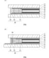
図1は、第1実施形態の液晶素子の構成を示す模式的な平面図である。また、図2(A)は、液晶素子の図1に示すA-A’方向の模式的な断面図であり、図2(B)は、液晶素子の図1に示すB-B’方向の模式的な断面図である。なお、図1ではシール部20の構造が分かりやすいように描画しているが実際にはシール部20は図2(A)及び図2(B)に示すように基板間(基板の内側)に存在する。First Embodiment
Fig. 1 is a schematic plan view showing the configuration of a liquid crystal element of the first embodiment. Fig. 2(A) is a schematic cross-sectional view of the liquid crystal element in the A-A' direction shown in Fig. 1, and Fig. 2(B) is a schematic cross-sectional view of the liquid crystal element in the B-B' direction shown in Fig. 1. Note that Fig. 1 depicts the structure of the
図2(A)及び図2(B)に示すように、液晶素子100aは、対向配置された第1基板11及び第2基板12、第1導電膜13、第2導電膜14、第1無機絶縁膜15、第2無機絶縁膜16、第1配向膜17、第2配向膜18、液晶層19、第1シール部21、第2シール部22、第3シール部23、導電材24、複数の突起部25、封止部26、27、28を含んで構成されている。なお、第1シール部21、第2シール部22、第3シール部23を含んでシール部20が構成されている。As shown in Figures 2(A) and 2(B), the
第1基板11及び第2基板12は、それぞれ、例えば平面視において矩形状の基板であり、互いの一面側が対向するようにして配置されている。各基板としては、例えばガラス基板、プラスチック基板等の透明な基板を用いることができる。各基板の板厚は、例えば0.7mm程度である。ここで、本明細書における「透明」とは、少なくとも可視光を十分に透過し得ることをいう。第1基板11と第2基板12の間には、例えば樹脂等からなる球状スペーサー(図示省略)が分散配置されており、それら球状スペーサーによって基板間隙が所望の大きさ(例えば数μm程度)に保たれている。なお、球状スペーサーに代えて、樹脂等からなる柱状体を第1基板11側若しくは第2基板12側に設け、それらをスペーサーとして用いてもよい。The
第1導電膜13は、第1基板11の一面側に設けられている。第2導電膜14は、第2基板12の一面側に設けられている。これらの第1導電膜13及び第2導電膜14は、例えばインジウム錫酸化物(ITO)などの酸化物からなる透明な導電膜を適宜パターニングすることによって構成されている。各導電膜の膜厚は、例えば280Å程度である。第1導電膜13と第2導電膜14との間に電圧が印加されることで液晶層19の配向状態を可変に設定することができる。第1導電膜13と第2導電膜14とが向かい合う部分において画素部(光変調部)が構成される。The first
第1無機絶縁膜15は、第1基板11の一面側において第1導電膜13の上側、すなわち第1導電膜13よりも第1基板11から遠い側に設けられている。第2無機絶縁膜16は、第2基板12の一面側において第2導電膜14の上側、すなわち第2導電膜14よりも第2基板12から遠い側に設けられている。本実施形態では、第1無機絶縁膜15及び第2無機絶縁膜16は、それぞれ無機材料を用いて成膜される。具体的には、第1無機絶縁膜15及び第2無機絶縁膜16は、シロキサン系無機絶縁膜、チタノシロキサン系無機絶縁膜などから構成することができる。また、シロキサン系無機絶縁膜、チタノシロキサン系無機絶縁膜は、それぞれ、ポリシロキサン系材料、ポリチタノシロキサン系材料を焼成することで形成することができる。特に、第1無機絶縁膜15及び第2無機絶縁膜16は、シロキサン系無機絶縁膜及びチタノシロキサン系無機絶縁膜であって、官能基にヒドロキシ基(OH基)を含む材料を好適に用いることができる。また、第1無機絶縁膜15及び第2無機絶縁膜16は、ITOからなる第1導電膜13や第2導電膜14と比較して高い緻密性を有している。各無機絶縁膜の膜厚は、例えば800Å程度である。The first inorganic
第1配向膜17は、第1基板の一面側において第1無機絶縁膜15の上側、すなわち第1無機絶縁膜15よりも第1基板11から遠い側に設けられている。第2配向膜18は、第2基板の一面側において第2無機絶縁膜16の上側、すなわち第2無機絶縁膜16よりも第2基板12から遠い側に設けられている。これらの第1配向膜17及び第2配向膜18は、液晶層19の初期配向状態を設定するためのものである。第1配向膜17及び第2配向膜18には、例えばラビング処理等の一軸配向処理が施されており、その方向に沿って液晶層19の液晶分子の配向を規定する一軸配向規制力を有している。各配向膜の膜厚は、例えば500Å程度である。第1配向膜17及び第2配向膜18は、ポリイミドなどの有機系材料、斜方蒸着法や印刷法で形成可能なシリコン酸化膜などの無機系材料から構成することができる。また、第1配向膜17及び第2配向膜18は、第1無機絶縁膜15及び第2無機絶縁膜16の材料と同様の基本骨格を有し適宜の官能基を備えた、シロキサン系配向膜から構成することができる。第1配向膜17及び第2配向膜18は、配向制御のための側鎖を有し、第1無機絶縁膜15及び第2無機絶縁膜16の材料と比較して少ないヒドロキシ基を含む材料を好適に用いることができる。The
液晶層19は、第1基板11と第2基板12の間において第1配向膜17及び第2配向膜18に接して設けられている。液晶層19は、例えば、流動性を有するネマティック液晶材料を用いて構成される。液晶層19の配向モード(動作モード)については特に限定がなく、垂直配向モード、捻れネマティックモードなど種々の配向モードを採用し得る。液晶層19の層厚は、例えば4μm程度である。The
シール部20は、第1基板11と第2基板12との間に液晶層19を囲んで配置されている。このシール部20は、図1に示すように液晶層19を収容するための空間を第1基板11と第2基板12との間に画定するものである。シール部20は、液晶層19と近い順に第1シール部21、第2シール部22及び第3シール部23を有する。図1に示すように、シール部20は、平面視において略矩形状に構成されており、第1基板11と第2基板12の各々の外縁に沿って配置されている。各シール部21、22、23には、例えば液晶層19の層厚よりもわずかに径の大きいグラスファイバー等のスペーサーが添加されていてもよい。The sealing
第1シール部21は、液晶層19に接して、液晶層19を囲むように設けられている。第1シール部21は、第1配向膜17の端部を覆うとともに第2配向膜18の端部を覆うように配置されている。詳細には、第1シール部21は、第1配向膜17の端部の段差状部分を覆ってその下側の第1無機絶縁膜15と接するように配置されるとともに、第2配向膜18の端部の段差状部分を覆ってその下側の第2無機絶縁膜16と接するように配置されている。第1シール部21は、液晶層19に不溶性で、接着性の高い材料で構成するのが好ましく、例えば、透湿度が50~70g/m2・24h(JISK7126-1)程度の熱硬化性エポキシ樹脂などの材料を用いることができる。 The
第2シール部22は、第1シール部21に接して、第1シール部21の外側を囲むように設けられている。第2シール部22は、第1無機絶縁膜15と第2無機絶縁膜16の各々と接するように配置されている。図2(A)に示すように、第2シール部22は、その大部分においては第1無機絶縁膜15及び第2無機絶縁膜16のみと接して密着するように設けられている。また、図2(B)に示すように、第2シール部22は、他の一部分においては第1基板11側において第1無機絶縁膜15及び第1導電膜13と接し、第2基板12側において第2無機絶縁膜16及び第2導電膜14と接するように設けられている。ここでいう一部分とは、第3シール部23において部分的に含まれる導電材24によって第1導電膜13と第2導電膜14の相互間が物理的及び電気的に接続される箇所に近接する部分である。第2シール部22は、透湿度の低い材料で構成するのが好ましく、特に、第1シール部21より透湿度の低い材料で構成するのが好ましい。例えば透湿度が2~4g/m2・24h(JISK7126-1)の材料を用いることが好ましく、例えば紫外線硬化性エポキシ、変性アクリレートなどの材料を用いることができる。 The
第3シール部23は、第2シール部22に接して、第2シール部22の外側を囲むように設けられている。第3シール部23は、図2(B)に示すように、その一部分において導電材24を有して当該導電材24が第1導電膜13及び第2導電膜14の各々と接するように配置され、図2(A)に示すように、他の大部分において第1無機絶縁膜13及び第2無機絶縁膜14の各々と接するように配置されている。導電材24は、例えば金メッキの施された球状体である。また、第3シール部23は、図2(A)に示すように、大部分において、第1導電膜13の端部、第1無機絶縁膜15の端部、第2導電膜14の端部及び第2無機絶縁膜16の端部を覆うように配置されている。つまり、図1に示す環状のシール部20の大部分において、図2(A)に示すように、第3シール部23は、第1無機絶縁膜15及び第2無機絶縁膜16の間を端部まで埋めるように形成されている。第3シール部23は、接着性の高い材料で構成するのが好ましく、例えば熱硬化性エポキシ樹脂などの材料を用いることができ、第1シール部21と同じ材料から構成することもできる。The
また、各図に示すように、第1シール部21、第2シール部22及び第3シール部23は、液晶層19の層厚方向と略直交する方向において互いに接して配置されている。詳細には、第2シール部22は、液晶層19と近い側において第1シール部21と接し、液晶層19から遠い側において第3シール部23と接して配置されている。また、第1シール部21と第3シール部23は、同一の材料からなる。第2シール部22は、第1シール部21及び第3シール部23よりも相対的に低い透湿性を有する。As shown in each figure, the
複数の突起部25は、図1に示すように第3シール部23の外周に沿って分散して設けられている。図示の例では、封止材26、27の近くの左右に2つの突起部25が設けられ、封止材28の近くの2つの突起部25が設けられている。これらの突起部25の機能については後述する。The
第1封止材26及び第2封止材27は、各々、製造時における液晶層19の注入口51(後述の図4(D)参照)を封止するためのエンドシール部である(図1参照)。第1封止材26としては、液晶層19の液晶材料に対する非相溶性を有するものが用いられる。また、第2封止材27としては、高いガスバリア性を有するものが用いられる。なお、2つの機能を併せ持つもの材料を用いる場合には、第1封止材26のみで足りる。The
第3封止材28は、製造時における第2シール部22の注入口52(後述の図4(C)参照)を封止するためのエンドシール部である(図1参照)。第3封止材28としては、高いガスバリア性を有するものが用いられる。なお、第3封止材28は任意に設けることができ、第2シール部22のガスバリア性が高い場合には不要とすることもできる。The
図3は、無機絶縁膜及び配向膜とシール部との配置関係を説明するための平面図である。なお、配置関係を示すために上記図1とはシール部等の縮尺を変えて示している。以下、この図3及び上記した図2(A)又は図2(B)を参照しながら、第1基板11の一面側での第1無機絶縁膜15及び第1配向膜17の各々の形成範囲について説明するとともに、第2基板12の一面側での第2無機絶縁膜16及び第2配向膜18の各々の形成範囲について説明する。Figure 3 is a plan view for explaining the positional relationship between the inorganic insulating film and the alignment film and the sealing portion. Note that the scale of the sealing portion is changed from that of Figure 1 in order to show the positional relationship. Below, with reference to Figure 3 and the above-mentioned Figure 2 (A) or Figure 2 (B), the formation ranges of the first inorganic insulating
図2(A)又は図2(B)に示すように、第1基板11の一面側において、第1導電膜13は、その端部が最も外側、すなわち第1基板11の端部に近い側まで設けられている部分を有してもよい。また、図2(A)又は図2(B)に示すように、第2基板12の一面側において、第2導電膜14は、その端部が第2配向膜18の端部とほぼ同じ位置まで設けられている部分を有してもよい。第1導電膜13、第2導電膜14ともに、それぞれの端部が第3シール部23と重なる場合もある。なお、第1導電膜13と第2導電膜14は、それぞれ適宜パターニングされている。例えば、第1導電膜13は、複数の画素電極やそれらと接続された複数の配線を含み得る。2(A) or 2(B), on one side of the
第1無機絶縁膜15は、その端部が第3シール部23の端部よりも内側(液晶層19に近い側)となるように設けられている(図3において点線で示す)。また、第1無機絶縁膜15は、図3に示すように切り欠き部15aを有している。この切り欠き部15aは、図2(B)に示す導電材24の設けられる部分に対応する位置に設けられており、第1導電膜13が第1無機絶縁膜15に覆われずに導電材24と接触できるようにするためのものである。同様の切り欠き部は第2無機絶縁膜16にも設けられている。第2無機絶縁膜16は、切り欠き部15aに対応する切り欠き部分ではその端部が第2導電膜14の端部よりも内側(液晶層19に近い側)となるように設けられている。第1無機絶縁膜15、第2無機絶縁膜16ともに、切り欠き部等に対応する部分を除く大部分でそれぞれの端部が第3シール部23と重なり、第3シール部23の外側端よりも内側に配置されている。The first inorganic insulating
第1配向膜17は、その端部が最も内側(液晶層19に近い側)となるように設けられている。同様に、第2配向膜18は、その端部が最も内側(液晶層19に近い側)となるように設けられている。第1配向膜17、第2配向膜18ともに、大部分でそれぞれの端部が第1シール部21と重なり、第1シール部21の外側端よりも内側に配置されている。The
図4(A)~図4(F)は、第1実施形態の液晶素子を製造する方法の一例を説明するための図である。なお、ここでは1つの液晶素子100aに係る工程を図示するが実際には複数の液晶素子100aを同時に製造することができる(他の実施形態においても同様)。Figures 4(A) to 4(F) are diagrams for explaining an example of a method for manufacturing the liquid crystal element of the first embodiment. Note that, although the process for one
まず、第1基板11、第2基板12の各々の母材となる一対の基板に、それぞれ第1導電膜13、第2導電膜14が形成される(図示省略)。第1導電膜13、第2導電膜14は適宜パターニングされてもよい。次に、図4(A)に示すように、第1基板11の母材50に対してその一面側に第1無機絶縁膜15(図示省略)と第1配向膜17が形成される。同様にして第2基板12の母材に対してその一面側に第2無機絶縁膜16(図示省略)と第2配向膜18が形成される(図示省略)。第1配向膜17、第2配向膜18としては、液晶層19の動作モード等に応じて水平配向膜や垂直配向膜が適宜選択され、形成される。First, a first
無機絶縁膜や配向膜の形成方法については特に限定がなく、例えばフレキソ印刷によって塗布され、その後焼成される。配向膜の配向処理についても特に限定がなく、例えばラビング処理を用いることができるが、他の方法(光配向処理など)であってもよい。また、各配向膜として斜方蒸着膜が用いられてもよい。また、各導電膜(電極)に開口部ないし突起部を設けてこれらによって斜め電界を生じさせることで液晶層19の配向制御を行うような動作モードの場合には、ラビング処理等の配向処理が省略される場合もある。なお、これらについては他の実施形態でも同様である。There are no particular limitations on the method of forming the inorganic insulating film and the alignment film; for example, they are applied by flexographic printing and then baked. There are no particular limitations on the alignment treatment of the alignment film; for example, a rubbing treatment can be used, but other methods (such as photoalignment treatment) may also be used. Also, obliquely evaporated films may be used as each alignment film. In addition, in the case of an operation mode in which openings or protrusions are provided in each conductive film (electrode) to generate an oblique electric field to control the alignment of the
図4(A)に示すように、第1基板11の母材50に対して、その一面側に第1配向膜17の形成された位置に対応して第1シール部21と第3シール部23が形成される。図示のように第1シール部21と第3シール部23は、相互間に隙間を空けて設けられる。この隙間は、後の工程で第2シール部22を設けるためのものである。第1シール部21と第3シール部23の形成方法については特に限定がなく、例えばディスペンサーを用いて塗布する方法や、スクリーン印刷によって塗布する方法などを用いることができる。このとき、注入口51、52としての開口がそれぞれ設けられる。また、このときに併せて、第1シール部21及び第3シール部23と同一材料によって各突起部25が形成される。As shown in FIG. 4A, the
次に、第1基板11の母材50と第2基板12の母材(図示せず)とを位置合わせして重ね合わせられる。このとき、第2基板12の母材には予めギャップコントロール材が散布される。第1シール部21と第3シール部23の特性に応じて、熱硬化性である場合には熱処理が行われ、光硬化性である場合には光照射処理が行われることで母材同士が貼り合わされる。その後、貼り合わされた母材に対して切断線(クラック)が入れられた後、切断線に沿って割断されることで、図4(B)に示すように、第1シール部21と第3シール部23に第1基板11と第2基板12が貼り合わせて構成されたセルが得られる。Next, the
次に、図4(C)に示すように第2シール部22が形成される。ここでは、第2シール部22の材料を注入口52の付近に滴下し、毛細管現象を利用して注入が行われる。その意味では、上記した第1シール部21と第3シール部23の隙間については毛細管現象を生じさせ得る程度の幅にしておく必要がある。第2シール部22の材料としては、透湿性の低いもの(ガスバリア性が高いもの)を用いる。例えば、透湿度が2~4g/m2・24h(JISK7126-1)の材料を用いることができる。また、注入時間の短縮という点では材料の粘性は低いほうが好ましく、例えば概ね10Pa・s以下の材料を用いることが好ましい。なお、粘性が高い材料を用いる場合であればセルを加熱しながら注入を行ってもよい。注入後、第2シール部22の特性に応じて、熱硬化性である場合には熱処理が行われ、光硬化性である場合には光照射処理が行われ、熱処理と光照射処理の双方が必要な場合は各処理が行われることで第2シール部22が完成する。一例として、365nmの波長を含む紫外線光を6J/cm2の条件で照射し、その後150℃で1時間の熱処理を行う。 Next, the
ここで、仮に注入口52から第2シール部22の材料があふれ出したとしても、注入口52の左右に設けられている突起部25と、反対側の注入口51の左右に設けられている突起部25により当該材料の流れが堰き止められる。もしこれらの突起部25がない場合には、第1基板11と第2基板12の外縁における隙間で毛細管現象が生じ、逆側の出口へ先回りしてしまい、第2シール部22を完全に充填できない場合が生じ得る。突起部25を設けることでそのような不具合を避けることができる。このため、突起部25は、第3シール部23の外周に沿ってより多くの数を設けることが好ましい。Even if the material of the
次に、図4(D)に示すように、注入口51から液晶材料が注入される。ここでは、真空注入法を用いる。具体的には、セルを真空チャンバー内に配置し、真空チャンバー内を低圧にした後、注入口51を注入タンク53の液晶材料に接するように配置する。その後、真空チャンバー内を大気圧に戻すことで注入口51から液晶材料が注入され、図4(E)に示すように液晶層19が形成される。液晶層19の液晶材料としては、動作モードに応じて誘電率異方性の正/負が適宜選択される。また、液晶材料には紫外線硬化性モノマーが添加されていてもよい。この場合、後に紫外線照射を行うことで高分子安定化された液晶層19が得られる。Next, as shown in FIG. 4(D), liquid crystal material is injected from the
次に、図4(E)に示すように、注入口51をシールするための封止材26が形成される。液晶材料を注入後のセルはその中央付近のセル厚が厚くなって膨らんでいる場合がある。この場合には、セルをプレスした状態で注入口51の付近に封止材26の材料を塗布し、その後にプレスを開放する。あるいは、セルを冷却する。これらにより、セル中心付近のセル厚が薄くなり、封止材26の材料が少し吸い込まれる。その後、光照射処理等によって材料を硬化させることで、注入口51から少し内部へ入り込んだ位置に封止材26が形成される。Next, as shown in FIG. 4(E), a
次に、図4(F)に示すように、注入口51の封止材26の外側に封止材27が形成されるとともに、注入口52に封止材28が形成される。具体的には、各封止材27、28の材料を注入口51、52の付近に塗布し、その後光照射処理等によって材料を硬化させることで、各封止材27、28が形成される。その後、セル全体の洗浄処理等を適宜行うことにより、液晶素子100aが完成する。Next, as shown in FIG. 4(F),
以上のような第1実施形態によれば、少なくとも第1シール部21と第2シール部22が第1無機絶縁膜15、第2無機絶縁膜16と接するように設けられるので、防湿性を高めることが可能となる。その理由は以下のように推測される。一般に、第1無機絶縁膜15及び第2無機絶縁膜16を構成するシロキサン系材料やチタノシロキサン系材料は、配向膜やITOなどの導電膜に比べ、その膜表面においてOH基を多く有していると考えられる。そして、このOH基が多いことにより、各シール部との密着性がより高くなることから、低透湿な第2シール部22の機能を維持することができ、透湿性の低いシール構造を構成することができたと考えられる。具体的には、各シール部の材料の有機官能基と第1無機絶縁膜15及び第2無機絶縁膜16を構成する材料のOH基との間で共有結合が生じることにより接合強度が向上する。また、第3シール部23も、第1無機絶縁膜15及び第2無機絶縁膜16の端部間を埋めるように設けられているので、同様にシール材の有機官能基と第1無機絶縁膜15及び第2無機絶縁膜16を構成する材料のOH基との間で共有結合を形成して接合強度を高めている。According to the first embodiment described above, at least the
また、第1実施形態によれば、シール部20が三重構造となることで、その平面視での幅が大きくなる(太くなる)ので、第1基板11と第2基板12をより強固に固定できるようになり、耐振動性が向上するという副次的効果も得られる。In addition, according to the first embodiment, the sealing
(第2実施形態)
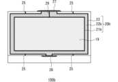
図5は、第2実施形態の液晶素子の構成を示す模式的な平面図である。第2実施形態の液晶素子100bは、基本的に第1実施形態の液晶素子100aと同様の構成を備えており、注入口51が省略されており、これに伴って封止材26も省略されている点が主に異なっている。この場合、液晶層19は、例えばODF(One Drop Fill)法によって形成される。以下では第1実施形態の液晶素子100aと構成の共通する点は説明を割愛し、構成の異なる点を主に説明する。Second Embodiment
5 is a schematic plan view showing the configuration of the liquid crystal element of the second embodiment. The
第1シール部21bは、注入口などの開口部を有しておらず、液晶層19を囲む閉空間を構成するように設けられている。また、これに伴い、第2シール部22bは、封止材27によって封止される2つの端部同士が隔壁29を介して隣り合うように設けられている。なお、これらを含むシール部20bの断面構造については第1実施形態と同様である(図2(A)、図2(B)参照)。各突起部25と隔壁29は、例えば第1シール部21bと同一材料によって形成されている。The
図6(A)~図6(D)は、第2実施形態の液晶素子を製造する方法の一例を説明するための図である。第1実施形態と同様に、予め、第1基板11、第2基板12の各々の母材となる一対の基板に、それぞれ第1導電膜13、第2導電膜14が形成される(図示省略)。Figures 6(A) to 6(D) are diagrams for explaining an example of a method for manufacturing a liquid crystal element of the second embodiment. As in the first embodiment, a first
次に、図6(A)に示すように、第1基板11の母材50に対してその一面側に第1無機絶縁膜15(図示省略)と第1配向膜17が形成される。同様にして第2基板12の母材に対してその一面側に第2無機絶縁膜16(図示省略)と第2配向膜18が形成される(図示省略)。Next, as shown in FIG. 6(A), a first inorganic insulating film 15 (not shown) and a
また、図6(A)に示すように、第1基板11の母材50に対して、その一面側に第1シール部21bと第3シール部23が形成される。このとき、注入口52としての開口が設けられる。また、第1シール部21bと同一材料によって各突起部25と隔壁29が形成される。As shown in FIG. 6A, the
次に、図6(B)に示すように、第1シール部21bに囲まれた空間にODF法などによって液晶材料が滴下される。液晶材料としては十分に脱泡したものを用い、滴下の体積は精密に制御される。次いで、第1基板11の母材50と第2基板12の母材(図示せず)とが位置合わせして重ねられ、貼り合わされる。その後、貼り合わされた母材に対して切断線(クラック)を入れた後、切断線に沿って割断されることで第1基板11と第2基板12が貼り合わせて構成されたセルが得られる。Next, as shown in FIG. 6(B), liquid crystal material is dropped into the space surrounded by the
次に、図6(C)に示すように第2シール部22bが形成される。ここでも、第2シール部22bの材料を注入口52の付近に滴下し、毛細管現象を利用して注入を行う。注入後、適宜、熱処理や光照射処理が行われることで第2シール部22bが完成する。このとき、図中において左回りに注入される材料と右回りに注入される材料が出口側で合流する際に、隔壁29があることで、注入スピードの差などによる不均衡が生じたとしても空気の逃げ道が確保されるので、第2シール部22bの形成不良を防止することができる。なお、注入スピードがほぼ同一であるような場合には隔壁29を省略してもよい。Next, the
次に、図6(D)に示すように、各封止材27、28の材料を所定位置に塗布し、その後光照射処理等によって材料を硬化させることで、各封止材27、28が形成される。その後、セル全体の洗浄処理等を適宜行うことにより、液晶素子100bが完成する。Next, as shown in FIG. 6(D), the material of each of the
以上のような第2実施形態によれば、第1実施形態と同様の防湿性が得られる。また、耐振動性の向上という副次的効果も得られる。さらに、第2実施形態によれば、液晶層19の形成にODF法などの真空注入法とは異なる方法を適用することができる。According to the second embodiment described above, moisture resistance similar to that of the first embodiment can be obtained. In addition, a secondary effect of improved vibration resistance can also be obtained. Furthermore, according to the second embodiment, a method other than the vacuum injection method, such as the ODF method, can be applied to form the
(第3実施形態)
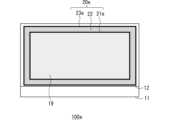
図7は、第3実施形態の液晶素子の構成を示す模式的な平面図である。第3実施形態の液晶素子100cは、基本的に第1実施形態の液晶素子100aと同様の構成を備えており、第1シール部21cと第3シール部23cとが封止材26、27の側で互いにつながっている点が主に異なっている。この場合、第2シール部22は、真空注入法を用いて形成される。以下では第1実施形態の液晶素子100aと構成の共通する点は説明を割愛し、構成の異なる点を主に説明する。Third Embodiment
7 is a schematic plan view showing the configuration of the liquid crystal element of the third embodiment. The
第1シール部21cは、注入口51、52を有し(図8(A)参照)、液晶層19を囲む略閉空間を構成するように設けられている。また、第3シール部23cは、第2シール部22の外周に沿って設けられており、注入口51の設けられている側で第1シール部21cとつながっている。なお、これらを含むシール部20cの断面構造については第1実施形態と同様である(図2(A)、図2(B)参照)。The
図8(A)~図8(F)は、第3実施形態の液晶素子を製造する方法の一例を説明するための図である。第1実施形態と同様に、予め、第1基板11、第2基板12の各々の母材となる一対の基板に、それぞれ第1導電膜13、第2導電膜14が形成される(図示省略)。Figures 8(A) to 8(F) are diagrams for explaining an example of a method for manufacturing a liquid crystal element of the third embodiment. As in the first embodiment, a first
次に、図8(A)に示すように、第1基板11の母材50に対してその一面側に第1無機絶縁膜15(図示省略)と第1配向膜17が形成される。同様にして第2基板12の母材に対してその一面側に第2無機絶縁膜16(図示省略)と第2配向膜18が形成される(図示省略)。Next, as shown in FIG. 8(A), a first inorganic insulating film 15 (not shown) and a
また、図8(A)に示すように、第1基板11の母材50に対して、その一面側に第1シール部21cと第3シール部23cが形成される。このとき、注入口51、52としての開口が設けられる。また、第3シール部23cと同一材料によって各突起部25が形成される。As shown in FIG. 8(A), the
次に、第1基板11の母材50と第2基板12の母材(図示せず)とが位置合わせして重ねられ、貼り合わされる。その後、貼り合わされた母材に対して切断線(クラック)を入れた後、切断線に沿って割断されることで第1基板11と第2基板12が貼り合わせて構成されたセルが得られる(図8(B)参照)。Next, the
次に、図8(C)に示すように第2シール部22が形成される。ここでは、真空注入法が用いられる。具体的には、セルを真空チャンバー内に配置し、真空チャンバー内を低圧にした後、注入口52を注入タンク54のシール材料に接するように配置する。その後、真空チャンバー内を大気圧に戻すことで注入口52からシール材料が注入される。注入後、適宜、熱処理や光照射処理が行われることで第2シール部22が完成する。Next, the
次に、図8(D)に示すように、真空注入法によってセルの注入口51を注入タンク53の液晶材料に接するように配置し、注入口51から液晶材料を注入し、液晶層19が形成される。Next, as shown in FIG. 8(D), the
次に、図8(E)、図8(F)に示すように、各封止材26、27、28の材料を所定位置に塗布し、その後光照射処理等によって材料を硬化させることで、各封止材26、27、28が形成される。その後、セル全体の洗浄処理等を適宜行うことにより、液晶素子100cが完成する。Next, as shown in Figures 8(E) and 8(F), the material for each of the
以上のような第3実施形態によれば、上記の各実施形態と同様の防湿性が得られる。また、耐振動性の向上という副次的効果も得られる。さらに、第3実施形態によれば、第2シール部22が外部に露出する部分を少なくすることができるので、防湿性を高めることができる。According to the third embodiment described above, moisture resistance similar to that of the above-mentioned embodiments can be obtained. In addition, a secondary effect of improved vibration resistance can be obtained. Furthermore, according to the third embodiment, the portion of the
(第4実施形態)
図9は、第4実施形態の液晶素子の構成を示す模式的な平面図である。第4実施形態の液晶素子100dは、基本的に第1実施形態の液晶素子100aと同様の構成を備えており、注入口51が省略され、これに伴って封止材26、27も省略されている点と、第3シール部23dの注入口52と反対側の部位が閉鎖している点が主に異なっている。この場合、第2シール部22については真空注入法によって形成され、液晶層19についてはODF(One Drop Fill)法によって形成される。以下では第1実施形態の液晶素子100aと構成の共通する点は説明を割愛し、構成の異なる点を主に説明する。Fourth Embodiment
9 is a schematic plan view showing the configuration of the liquid crystal element of the fourth embodiment. The
第1シール部21dは、注入口などの開口部を有しておらず、液晶層19を囲む閉空間を構成するように設けられている。また、第3シール部23dは、開口部52(図10(A)参照)を有し、第1シール部21dと隙間を空けて設けられている。なお、これらを含むシール部20dの断面構造については第1実施形態と同様である(図2(A)、図2(B)参照)。The
図10(A)~図10(D)は、第4実施形態の液晶素子を製造する方法の一例を説明するための図である。第1実施形態と同様に、予め、第1基板11、第2基板12の各々の母材となる一対の基板に、それぞれ第1導電膜13、第2導電膜14が形成される(図示省略)。また、第1基板11の母材50に対してその一面側に第1無機絶縁膜15(図示省略)と第1配向膜17が形成され、第2基板12の母材に対してその一面側に第2無機絶縁膜16(図示省略)と第2配向膜18が形成される(図示省略)。Figures 10(A) to 10(D) are diagrams for explaining an example of a method for manufacturing a liquid crystal element of the fourth embodiment. As in the first embodiment, a first
次に、図10(A)に示すように、第1基板11の母材50に対して、その一面側に第1シール部21dと第3シール部23dが形成される。このとき、注入口52としての開口が設けられる。また、第3シール部23dと同一材料によって各突起部25が形成される。Next, as shown in FIG. 10(A), the
次に、図10(B)に示すように、第1シール部21dに囲まれた空間にODF法などによって液晶材料が滴下されることにより液晶層19が形成される。次いで、第1基板11の母材50と第2基板12の母材(図示せず)とが位置合わせして重ねられ、貼り合わされる。その後、貼り合わされた母材に対して切断線(クラック)を入れた後、切断線に沿って割断されることで第1基板11と第2基板12が貼り合わせて構成されたセルが得られる。Next, as shown in FIG. 10(B), a liquid crystal material is dropped into the space surrounded by the
次に、図10(C)に示すように第2シール部22が形成される。ここでは上記した第3実施形態と同様に注入タンク54を用いて真空注入法によりシール材料が注入される。それにより、第2シール部22が完成する。Next, the
次に、図10(D)に示すように、封止材28の材料を所定位置に塗布し、その後光照射処理等によって材料を硬化させることで封止材28が形成される。その後、セル全体の洗浄処理等を適宜行うことにより、液晶素子100dが完成する。Next, as shown in FIG. 10(D), the material for the
以上のような第4実施形態によれば、上記の各実施形態と同様の防湿性が得られる。また、耐振動性の向上という副次的効果も得られる。さらに、第4実施形態によれば、第2シール部22が外部に露出する部分を少なくすることができるので、防湿性を高めることができる。According to the fourth embodiment described above, moisture resistance similar to that of the above-mentioned embodiments can be obtained. In addition, a secondary effect of improved vibration resistance can be obtained. Furthermore, according to the fourth embodiment, the portion of the
(第5実施形態)
図11は、第5実施形態の液晶素子の構成を示す模式的な平面図である。第5実施形態の液晶素子100eは、基本的に第1実施形態の液晶素子100aと同様の構成を備えており、注入口51、52が省略されて第1シール部21e及び第3シール部23eがともに閉空間を構成しており、これに伴って封止材26、27、28も省略されている点が主に異なっている。この場合、第2シール部22、液晶層19ともにODF(One Drop Fill)法によって形成される。以下では第1実施形態の液晶素子100aと構成の共通する点は説明を割愛し、構成の異なる点を主に説明する。Fifth Embodiment
11 is a schematic plan view showing the configuration of the liquid crystal element of the fifth embodiment. The
第1シール部21eは、注入口などの開口部を有しておらず、液晶層19を囲む閉空間を構成するように設けられている。第3シール部23eは、注入口などの開口部を有しておらず、閉空間を構成するようにして、第1シール部21eと隙間を空けて設けられている。なお、これらを含むシール部20eの断面構造については第1実施形態と同様である(図2(A)、図2(B)参照)。The
図12(A)~図12(C)は、第5実施形態の液晶素子を製造する方法の一例を説明するための図である。第1実施形態と同様に、予め、第1基板11、第2基板12の各々の母材となる一対の基板に、それぞれ第1導電膜13、第2導電膜14が形成される(図示省略)。また、第1基板11の母材50に対してその一面側に第1無機絶縁膜15(図示省略)と第1配向膜17が形成され、第2基板12の母材に対してその一面側に第2無機絶縁膜16(図示省略)と第2配向膜18が形成される(図示省略)。Figures 12(A) to 12(C) are diagrams for explaining an example of a method for manufacturing a liquid crystal element of the fifth embodiment. As in the first embodiment, a first
次に、図12(A)に示すように、第1基板11の母材50に対して、その一面側に第1シール部21eと第3シール部23eが形成される。そして、第1シール部21eに囲まれた空間にODF法などによって液晶材料が滴下されることにより液晶層19が形成される。Next, as shown in FIG. 12(A), a
次に、図12(B)に示すように、第1シール部21aと第3シール部23eの隙間に、ODF法などによってシール材料が滴下されることにより第2シール部22が形成される。Next, as shown in FIG. 12(B), a sealing material is dripped into the gap between the first seal portion 21a and the
次いで、第1基板11の母材50と第2基板12の母材(図示せず)とが位置合わせして重ねられ、貼り合わされる。その後、貼り合わされた母材に対して切断線(クラック)を入れた後、切断線に沿って割断されることで第1基板11と第2基板12が貼り合わせて構成されたセルが得られる。その後、セル全体の洗浄処理等を適宜行うことにより、液晶素子100eが完成する。Next, the
以上のような第5実施形態によれば、上記の各実施形態と同様の防湿性が得られる。また、耐振動性の向上という副次的効果も得られる。さらに、第5実施形態によれば、第2シール部22が外部に露出する部分をなくし、すべての外周を第3シール部23eで囲むことができるので、防湿性をさらに高めることができる。According to the fifth embodiment described above, moisture resistance similar to that of the above-mentioned embodiments can be obtained. In addition, a secondary effect of improved vibration resistance can be obtained. Furthermore, according to the fifth embodiment, the
(第6実施形態)
図13は、第6実施形態の車両用灯具システムの構成を示す図である。図13に示す車両用灯具システムは、上記のいずれかの実施形態に係る液晶素子100a~100eを用いて構成されるものであり、ランプユニット(車両用灯具)101と、コントローラ102と、カメラ103を含んで構成されている。この車両用前照灯システムは、カメラ103によって撮影される画像に基づいて自車両の周囲に存在する前方車両や歩行者の顔等の位置を検出し、前方車両等の位置を含む一定範囲を非照射範囲(減光領域)に設定し、それ以外の範囲を光照射範囲に設定して選択的な光照射を行うとともに、路面上へ種々形状の光照射を行うものである。Sixth Embodiment
Fig. 13 is a diagram showing the configuration of a vehicle lamp system according to a sixth embodiment. The vehicle lamp system shown in Fig. 13 is configured using the
ランプユニット101は、車両前部の所定位置に配置されており、車両前方を照明するための照射光を形成する。なお、ランプユニット101は車両の左右それぞれに1つずつ設けられるがここでは1つのみ図示する。The
コントローラ102は、車両用灯具101の光源110や液晶素子115の動作制御を行うものである。このコントローラ102は、例えばCPU(Central Processing Unit)、ROM(Read Only Memory)、RAM(Random Access Memory)等を有するコンピュータシステムを用い、このコンピュータシステムにおいて所定の動作プログラムを実行させることによって実現される。本実施形態のコントローラ102は、運転席に設置されたライトスイッチ(図示せず)の操作状態に応じて光源110を点灯させるとともに、カメラ103によって検出される前方車両(対向車両、先行車両)、歩行者、道路標識、路上白線などの対象体に応じた配光パターンを設定し、この配光パターンに対応する像を形成するための制御信号を液晶素子115へ供給する。The
カメラ103は、自車両の前方空間を撮影して画像を生成し、この画像に対して所定の画像認識処理を行って上記した前方車両等の対象体の位置、範囲、大きさ、種別などを検出する。画像認識処理による検出結果は、カメラ103と接続されているコントローラ102へ供給される。カメラ103は、自車両の車室内の所定位置(例えば、フロントガラス上部)に設置されるか、または自車両の車室外の所定位置(例えば、フロントバンパー内)に設置される。車両に他の用途(例えば、自動ブレーキシステム等)のためのカメラが備わっている場合にはそのカメラを共用してもよい。The
なお、カメラ103における画像認識処理の機能をコントローラ102にて代替してもよい。その場合には、カメラ103は、生成した画像をコントローラ102へ出力、この画像に基づいてコントローラ102側で画像認識処理が行われる。あるいは、カメラ103から画像とそれに基づく画像認処理の結果の双方がコントローラ102へ供給されてもよい。その場合に、コントローラ102は、カメラ103から得た画像を用いてさらに独自の画像認識処理を行ってもよい。The image recognition processing function in the
図13に示すランプユニット101は、光源110、リフレクタ111、113、偏光ビームスプリッタ112、1/4波長板114、液晶素子115、光学補償板116、偏光板117、投影レンズ118を含んで構成されている。これらの各要素は、例えば1つのハウジング(筐体)に収容されて一体化されている。また、光源110と液晶素子115は、それぞれコントローラ102と接続されている。なお、本実施形態では、偏光ビームスプリッタ112と偏光板117が「偏光素子」に対応する。The
光源110は、コントローラ102による制御を受けて光を放出する。この光源110は、例えばいくつかの白色LED(Light Emitting Diode)などの発光素子と駆動回路を含んで構成される。なお、光源110の構成はこれに限定されない。例えば、なお、光源110としては、レーザ素子、さらには電球や放電灯など車両用ランプユニットに一般的に使用されている光源が使用可能である。The
リフレクタ111は、光源110に対応づけて配置されており、光源110から放出される光を反射及び集光して偏光ビームスプリッタ112の方向へ導き、液晶素子115へ入射させる。リフレクタ111は、例えば楕円面状の反射面を有する反射鏡である。この場合、光源110は、リフレクタ111の反射面の焦点付近に配置することができる。なお、リフレクタ111に代えて集光部として集光レンズを用いてもよい。The
偏光ビームスプリッタ112は、入射光のうち特定方向の偏光成分を透過し、これと直交方向の偏光成分を反射させる反射型偏光素子である。このような偏光ビームスプリッタ112としては、例えばワイヤーグリッド型偏光素子や多層膜偏光素子などを用いることができる。The
リフレクタ113は、偏光ビームスプリッタ112によって反射される光が入射し得る位置に設けられており、入射した光を偏光ビームスプリッタ112の方向へ反射させる。The
1/4波長板114は、偏光ビームスプリッタ112とリフレクタ113の間の光路上に配置されており、入射する光に位相差を与える。本実施形態では、偏光ビームスプリッタ112によって反射された光は、1/4波長板114を透過し、リフレクタ113で反射されて再度1/4波長板114を透過することで偏光方向が90°回転して偏光ビームスプリッタ112へ再入射する。それにより、再入射した光は偏光ビームスプリッタ112を透過することができるので光の利用効率が向上する。The quarter-
液晶素子115は、リフレクタ111、113のそれぞれにより反射及び集光された光が入射し得る位置に配置されている。液晶素子115は、互いに独立に制御可能な複数の画素部(光変調部)を備えている。本実施形態では、液晶素子115は、各画素部に駆動電圧を与えるためのドライバ(図示せず)を有している。ドライバは、コントローラ102から供給される制御信号に基づいて、液晶素子115に対して、各画素部を個別に駆動するための駆動電圧を与える。この液晶素子115として、上記の各実施形態に係る液晶素子100a~100eのいずれかが用いられる。The
光学補償板116は、液晶素子115を透過した光の位相差を補償し、偏光度を高めるためのものである。なお、光学補償板116は省略されてもよい。The
偏光板117は、液晶素子115の光出射側に配置されている。偏光ビームスプリッタ112、偏光板117とこれらの間に配置された液晶素子115によって、自車両の前方へ照射する光の配光パターンに対応した像が形成される。The
投影レンズ118は、リフレクタ111、113により反射及び集光され、液晶素子115を透過した光が入射し得る位置に配置されており、この入射した光を自車両の前方へ投影する。投影レンズ118は、その焦点が液晶素子115の液晶層の位置に対応するように配置されている。The
以上のような第6実施形態によれば、防湿性に優れた液晶素子を備える車両用灯具並びに車両用灯具システムを得ることができる。According to the sixth embodiment described above, it is possible to obtain a vehicle lamp and a vehicle lamp system equipped with a liquid crystal element having excellent moisture resistance.
(変形例)
なお、本開示は上記した各実施形態の内容に限定されるものではなく、本開示の要旨の範囲内において種々に変形して実施をすることが可能である。例えば、車両用灯具システムの構成は上記した第6実施形態の構成に限定されず、液晶素子を用いて配光パターンを形成するものであれば本開示に係る液晶素子を適用することができる。また、各実施形態の液晶素子は、車両用途に限らず種々の照明装置(例えば液晶プロジェクタ等)に適用することも可能であり、また一般的な表示用途の液晶素子に適用することも可能である。(Modification)
The present disclosure is not limited to the contents of the above-mentioned embodiments, and can be modified in various ways within the scope of the gist of the present disclosure. For example, the configuration of the vehicle lighting system is not limited to the configuration of the sixth embodiment, and the liquid crystal element according to the present disclosure can be applied as long as the light distribution pattern is formed using a liquid crystal element. In addition, the liquid crystal element of each embodiment can be applied to various lighting devices (e.g., liquid crystal projectors, etc.) other than vehicle applications, and can also be applied to liquid crystal elements for general display applications.
11:第1基板、12:第2基板、13:第1導電膜、14:第2導電膜、15:第1無機絶縁膜、16:第2無機絶縁膜、17:第1配向膜、18:第2配向膜、19:液晶層、20:シール部、21:第1シール部、22:第2シール部、23:第3シール部、24:導電材、25:突起部、26、27、28:封止部、100a:液晶素子11: First substrate, 12: Second substrate, 13: First conductive film, 14: Second conductive film, 15: First inorganic insulating film, 16: Second inorganic insulating film, 17: First alignment film, 18: Second alignment film, 19: Liquid crystal layer, 20: Sealing portion, 21: First sealing portion, 22: Second sealing portion, 23: Third sealing portion, 24: Conductive material, 25: Protrusion portion, 26, 27, 28: Sealing portion, 100a: Liquid crystal element
Claims (10)
Translated fromJapanese前記第1基板の一面側に配置される第1導電膜と、
前記第1基板の一面側において前記第1導電膜よりも前記第1基板から遠い側に配置される第1無機絶縁膜と、
前記第1基板の一面側において前記第1無機絶縁膜よりも前記第1基板から遠い側に配置される第1配向膜と、
前記第2基板の一面側に配置される第2導電膜と、
前記第2基板の一面側において前記第2導電膜よりも前記第2基板から遠い側に配置される第2無機絶縁膜と、
前記第2基板の一面側において前記第2無機絶縁膜よりも前記第2基板から遠い側に配置される第2配向膜と、
前記第1基板と前記第2基板の間に配置される液晶層と、
前記第1基板と前記第2基板との間に前記液晶層を囲んで配置されるシール部と、
を含み、
前記シール部は、前記液晶層と近い順に少なくとも第1シール部及び第2シール部を有しており、
前記第1シール部は、前記第1配向膜の端部を覆うとともに前記第2配向膜の端部を覆うように配置されており、
前記第2シール部は、前記第1無機絶縁膜と前記第2無機絶縁膜の各々と接するように配置されている、
液晶素子。 A first substrate and a second substrate disposed opposite each other;
A first conductive film disposed on one surface side of the first substrate;
a first inorganic insulating film disposed on one surface side of the first substrate farther from the first substrate than the first conductive film;
a first alignment film disposed on one surface side of the first substrate, the first alignment film being farther from the first substrate than the first inorganic insulating film;
A second conductive film disposed on one surface side of the second substrate;
a second inorganic insulating film disposed on one surface side of the second substrate farther from the second substrate than the second conductive film;
a second alignment film disposed on one surface side of the second substrate, the second alignment film being farther from the second substrate than the second inorganic insulating film;
a liquid crystal layer disposed between the first substrate and the second substrate;
a seal portion disposed between the first substrate and the second substrate to surround the liquid crystal layer;
Including,
the sealing portion includes at least a first sealing portion and a second sealing portion in the order of proximity to the liquid crystal layer,
the first sealing portion is disposed so as to cover an end portion of the first alignment film and an end portion of the second alignment film;
the second sealing portion is disposed so as to be in contact with each of the first inorganic insulating film and the second inorganic insulating film;
Liquid crystal element.
請求項1に記載の液晶素子。 the first sealing portion is disposed so as to cover a stepped portion of an end portion of the first alignment film and to be in contact with the first inorganic insulating film, and is disposed so as to cover a stepped portion of an end portion of the second alignment film and to be in contact with the second inorganic insulating film;
The liquid crystal device according to claim 1 .
請求項1又は2に記載の液晶素子。 Each of the first inorganic insulating film and the second inorganic insulating film is made of a siloxane-based material or a titanosiloxane-based material.
3. A liquid crystal device according to claim 1 or 2.
請求項1~3の何れか1項に記載の液晶素子。 The material constituting the second seal portion has a relatively lower moisture permeability than the material constituting the first seal portion.
4. A liquid crystal device according to claim 1.
前記第3シール部は、その一部において導電材を有して当該導電材が前記第1導電膜及び前記第2導電膜の各々と接するように配置され、他の一部において前記第1無機絶縁膜及び前記第2無機絶縁膜の各々と接するように配置されている、
請求項1~4の何れか1項に記載の液晶素子。 the sealing portion further includes a third sealing portion disposed at a position farther from the liquid crystal layer than the second sealing portion,
the third seal portion has a conductive material in a part thereof and is arranged so that the conductive material is in contact with each of the first conductive film and the second conductive film, and is arranged so that the third seal portion is in contact with each of the first inorganic insulating film and the second inorganic insulating film in another part thereof.
5. A liquid crystal device according to claim 1.
請求項5に記載の液晶素子。 the third sealing portion is disposed so as to cover an end portion of the first conductive film, an end portion of the first inorganic insulating film, an end portion of the second conductive film, and an end portion of the second inorganic insulating film in the other part.
The liquid crystal device according to claim 5 .
請求項5又は6に記載の液晶素子。 The first seal portion and the third seal portion are made of the same material.
7. A liquid crystal device according to claim 5.
請求項5~7の何れか1項に記載の液晶素子。 the first seal portion and the third seal portion are in close contact with the second seal portion in a direction substantially perpendicular to a thickness direction of the liquid crystal layer;
The liquid crystal device according to any one of claims5 to 7.
前記液晶素子を挟んで対向配置される一対の偏光素子と、
前記液晶素子へ光を入射させる光源と、
を含む、照明装置。 A liquid crystal element according to any one of claims 1 to 8,
a pair of polarizing elements disposed opposite to each other with the liquid crystal element therebetween;
a light source that causes light to be incident on the liquid crystal element;
13. A lighting device comprising:
Priority Applications (2)
| Application Number | Priority Date | Filing Date | Title |
|---|---|---|---|
| JP2021087213AJP7590922B2 (en) | 2021-05-24 | 2021-05-24 | Liquid crystal elements, lighting devices, vehicle lights |
| CN202210544296.8ACN115390318A (en) | 2021-05-24 | 2022-05-19 | Liquid crystal devices, lighting devices, vehicle lamps |
Applications Claiming Priority (1)
| Application Number | Priority Date | Filing Date | Title |
|---|---|---|---|
| JP2021087213AJP7590922B2 (en) | 2021-05-24 | 2021-05-24 | Liquid crystal elements, lighting devices, vehicle lights |
Publications (2)
| Publication Number | Publication Date |
|---|---|
| JP2022180226A JP2022180226A (en) | 2022-12-06 |
| JP7590922B2true JP7590922B2 (en) | 2024-11-27 |
Family
ID=84115714
Family Applications (1)
| Application Number | Title | Priority Date | Filing Date |
|---|---|---|---|
| JP2021087213AActiveJP7590922B2 (en) | 2021-05-24 | 2021-05-24 | Liquid crystal elements, lighting devices, vehicle lights |
Country Status (2)
| Country | Link |
|---|---|
| JP (1) | JP7590922B2 (en) |
| CN (1) | CN115390318A (en) |
Citations (9)
| Publication number | Priority date | Publication date | Assignee | Title |
|---|---|---|---|---|
| JP2006309129A (en) | 2005-03-28 | 2006-11-09 | Seiko Epson Corp | Seal structure, sealing method, liquid crystal device, manufacturing method thereof, and projector |
| JP2009251565A (en) | 2008-04-11 | 2009-10-29 | Hitachi Displays Ltd | Method for manufacturing liquid crystal display device |
| JP2011158861A (en) | 2010-02-04 | 2011-08-18 | Seiko Epson Corp | Electro-optical device and electronic equipment |
| WO2011125273A1 (en) | 2010-04-01 | 2011-10-13 | シャープ株式会社 | Method for manufacturing liquid crystal display panel, and liquid crystal display panel manufactured by the method |
| JP2012220523A (en) | 2011-04-04 | 2012-11-12 | Seiko Epson Corp | Liquid crystal device and projector |
| JP2013025125A (en) | 2011-07-22 | 2013-02-04 | Japan Display Central Co Ltd | Display device |
| JP2013218234A (en) | 2012-04-12 | 2013-10-24 | Seiko Epson Corp | Electro-optic device and electronic equipment |
| CN105549272A (en) | 2016-01-29 | 2016-05-04 | 武汉华星光电技术有限公司 | Packaging structure and method of display panel |
| US20210096433A1 (en) | 2019-09-26 | 2021-04-01 | Samsung Display Co., Ltd. | Display substrate, display device having the same, and method of manufacturing the display substrate |
- 2021
- 2021-05-24JPJP2021087213Apatent/JP7590922B2/enactiveActive
- 2022
- 2022-05-19CNCN202210544296.8Apatent/CN115390318A/enactivePending
Patent Citations (9)
| Publication number | Priority date | Publication date | Assignee | Title |
|---|---|---|---|---|
| JP2006309129A (en) | 2005-03-28 | 2006-11-09 | Seiko Epson Corp | Seal structure, sealing method, liquid crystal device, manufacturing method thereof, and projector |
| JP2009251565A (en) | 2008-04-11 | 2009-10-29 | Hitachi Displays Ltd | Method for manufacturing liquid crystal display device |
| JP2011158861A (en) | 2010-02-04 | 2011-08-18 | Seiko Epson Corp | Electro-optical device and electronic equipment |
| WO2011125273A1 (en) | 2010-04-01 | 2011-10-13 | シャープ株式会社 | Method for manufacturing liquid crystal display panel, and liquid crystal display panel manufactured by the method |
| JP2012220523A (en) | 2011-04-04 | 2012-11-12 | Seiko Epson Corp | Liquid crystal device and projector |
| JP2013025125A (en) | 2011-07-22 | 2013-02-04 | Japan Display Central Co Ltd | Display device |
| JP2013218234A (en) | 2012-04-12 | 2013-10-24 | Seiko Epson Corp | Electro-optic device and electronic equipment |
| CN105549272A (en) | 2016-01-29 | 2016-05-04 | 武汉华星光电技术有限公司 | Packaging structure and method of display panel |
| US20210096433A1 (en) | 2019-09-26 | 2021-04-01 | Samsung Display Co., Ltd. | Display substrate, display device having the same, and method of manufacturing the display substrate |
Also Published As
| Publication number | Publication date |
|---|---|
| JP2022180226A (en) | 2022-12-06 |
| CN115390318A (en) | 2022-11-25 |
Similar Documents
| Publication | Publication Date | Title |
|---|---|---|
| JP5912712B2 (en) | Optical system for illumination | |
| US10914444B2 (en) | Lamp unit, vehicular lamp system | |
| JP5576751B2 (en) | Vehicle lighting | |
| CN109937321A (en) | headlight device | |
| KR20110037905A (en) | Method of manufacturing light irradiation apparatus and light deflection liquid crystal cell | |
| JP2012069458A (en) | Lighting fixture for vehicle | |
| JP2011258500A (en) | Vehicular lighting fixture | |
| US12392469B2 (en) | Lighting apparatus with liquid crystal element tilted with respect to the optical axis of the projection lens, vehicle lamp system having the same and lighting apparatus with prisms to refract a traveling direction before and after a liquid crystal element | |
| JP7590922B2 (en) | Liquid crystal elements, lighting devices, vehicle lights | |
| JP6854179B2 (en) | Lamp unit, vehicle lighting system | |
| JP2021150016A (en) | Lamp unit, vehicular lighting fixture system | |
| JP7202934B2 (en) | Liquid crystal element, lighting device | |
| US12297973B2 (en) | Lighting apparatus, and vehicle lamp system | |
| JP6854180B2 (en) | Lamp unit, vehicle lighting system | |
| JP2022167222A (en) | Liquid crystal element, lighting figure for vehicles, and lighting fixture system for vehicles | |
| JP2010145646A (en) | Light irradiation device | |
| JP2021096996A (en) | Vehicular lighting system | |
| JP7744225B2 (en) | Lighting device, vehicle lighting system | |
| JP7714451B2 (en) | Liquid crystal elements, lighting devices | |
| US12216361B2 (en) | Liquid crystal element, lighting apparatus, and vehicle lamp system | |
| US20230392765A1 (en) | Vehicular lamp and optical element | |
| JP2023177001A (en) | Lighting device and vehicle lamp system | |
| JP2024087475A (en) | Light Projection System | |
| JP2024164495A (en) | Method for manufacturing liquid crystal element, liquid crystal element, lighting device, and vehicle lighting system | |
| JP2022183784A (en) | liquid crystal element, liquid crystal device, lighting device |
Legal Events
| Date | Code | Title | Description |
|---|---|---|---|
| A621 | Written request for application examination | Free format text:JAPANESE INTERMEDIATE CODE: A621 Effective date:20240401 | |
| A977 | Report on retrieval | Free format text:JAPANESE INTERMEDIATE CODE: A971007 Effective date:20240905 | |
| A131 | Notification of reasons for refusal | Free format text:JAPANESE INTERMEDIATE CODE: A131 Effective date:20240910 | |
| A521 | Request for written amendment filed | Free format text:JAPANESE INTERMEDIATE CODE: A523 Effective date:20241007 | |
| TRDD | Decision of grant or rejection written | ||
| A01 | Written decision to grant a patent or to grant a registration (utility model) | Free format text:JAPANESE INTERMEDIATE CODE: A01 Effective date:20241025 | |
| A61 | First payment of annual fees (during grant procedure) | Free format text:JAPANESE INTERMEDIATE CODE: A61 Effective date:20241115 | |
| R150 | Certificate of patent or registration of utility model | Ref document number:7590922 Country of ref document:JP Free format text:JAPANESE INTERMEDIATE CODE: R150 |