JP7588516B2 - Plasma Processing Equipment - Google Patents
Plasma Processing EquipmentDownload PDFInfo
- Publication number
- JP7588516B2 JP7588516B2JP2021012816AJP2021012816AJP7588516B2JP 7588516 B2JP7588516 B2JP 7588516B2JP 2021012816 AJP2021012816 AJP 2021012816AJP 2021012816 AJP2021012816 AJP 2021012816AJP 7588516 B2JP7588516 B2JP 7588516B2
- Authority
- JP
- Japan
- Prior art keywords
- bias
- source
- power
- power level
- signal
- Prior art date
- Legal status (The legal status is an assumption and is not a legal conclusion. Google has not performed a legal analysis and makes no representation as to the accuracy of the status listed.)
- Active
Links
- 239000000758substrateSubstances0.000claims6
Images


Classifications
- H—ELECTRICITY
- H01—ELECTRIC ELEMENTS
- H01J—ELECTRIC DISCHARGE TUBES OR DISCHARGE LAMPS
- H01J37/00—Discharge tubes with provision for introducing objects or material to be exposed to the discharge, e.g. for the purpose of examination or processing thereof
- H01J37/32—Gas-filled discharge tubes
- H01J37/32009—Arrangements for generation of plasma specially adapted for examination or treatment of objects, e.g. plasma sources
- H01J37/32082—Radio frequency generated discharge
- H01J37/32174—Circuits specially adapted for controlling the RF discharge
- H—ELECTRICITY
- H01—ELECTRIC ELEMENTS
- H01J—ELECTRIC DISCHARGE TUBES OR DISCHARGE LAMPS
- H01J37/00—Discharge tubes with provision for introducing objects or material to be exposed to the discharge, e.g. for the purpose of examination or processing thereof
- H01J37/32—Gas-filled discharge tubes
- H01J37/32009—Arrangements for generation of plasma specially adapted for examination or treatment of objects, e.g. plasma sources
- H01J37/32082—Radio frequency generated discharge
- H01J37/32137—Radio frequency generated discharge controlling of the discharge by modulation of energy
- H01J37/32146—Amplitude modulation, includes pulsing
- H—ELECTRICITY
- H01—ELECTRIC ELEMENTS
- H01J—ELECTRIC DISCHARGE TUBES OR DISCHARGE LAMPS
- H01J37/00—Discharge tubes with provision for introducing objects or material to be exposed to the discharge, e.g. for the purpose of examination or processing thereof
- H01J37/32—Gas-filled discharge tubes
- H01J37/32431—Constructional details of the reactor
- H01J37/32715—Workpiece holder
- H—ELECTRICITY
- H01—ELECTRIC ELEMENTS
- H01J—ELECTRIC DISCHARGE TUBES OR DISCHARGE LAMPS
- H01J2237/00—Discharge tubes exposing object to beam, e.g. for analysis treatment, etching, imaging
- H01J2237/32—Processing objects by plasma generation
- H01J2237/33—Processing objects by plasma generation characterised by the type of processing
- H01J2237/334—Etching
- H01J2237/3341—Reactive etching
Landscapes
- Physics & Mathematics (AREA)
- Engineering & Computer Science (AREA)
- Plasma & Fusion (AREA)
- Chemical & Material Sciences (AREA)
- Analytical Chemistry (AREA)
- Plasma Technology (AREA)
- Drying Of Semiconductors (AREA)
Description
Translated fromJapanese以下の開示は、プラズマ処理装置に関する。The following disclosure relates to a plasma processing apparatus.
特許文献1は、誘導結合型プラズマ(Inductively Coupled Plasma: ICP、トランス結合型プラズマ(Transformer Coupled Plasma: TCP)とも呼ぶ。)を用いた装置においてRF(Radio Frequency)信号をパルス化する技術が開示されている。この特許文献1は、例えば、コイルに供給するソースRF信号とチャックに供給するバイアスRF信号とをパルスシーケンスが逆になるように同期させることを開示している。
本開示は、プラズマエッチングの処理性能を向上させることができる技術を提供する。This disclosure provides technology that can improve the processing performance of plasma etching.
本開示の一態様によるプラズマ処理装置は、プラズマ処理チャンバと、基板支持部と、ソースRF生成部と、バイアスRF生成部と、を備える。基板支持部は、プラズマ処理チャンバ内に配置される。ソースRF生成部は、プラズマ処理チャンバに結合され、ソースRF信号を生成するように構成される。ソースRF信号は、複数のソースサイクルを含み、各ソースサイクルは、ソースオン状態及びソースオフ状態を含む。ソースオン状態は、少なくとも2つのソースパワーレベルを有する。バイアスRF生成部は、バイアスRF信号を下部電極に供給するように構成される。バイアスRF信号は、複数のソースサイクルにそれぞれ対応する複数のバイアスサイクルを含む。各バイアスサイクルは、バイアスオン状態及びバイアスオフ状態を含む。バイアスオン状態は、少なくとも2つのバイアスパワーレベルを有する。第1のバイアスサイクルにおけるバイアスオン状態への遷移タイミングは、第1のバイアスサイクルに対応する第1のソースサイクルにおけるソースオン状態への遷移タイミングに対してずらされる。A plasma processing apparatus according to an aspect of the present disclosure includes a plasma processing chamber, a substrate support, a source RF generating unit, and a bias RF generating unit. The substrate support is disposed within the plasma processing chamber. The source RF generating unit is coupled to the plasma processing chamber and configured to generate a source RF signal. The source RF signal includes a plurality of source cycles, each of which includes a source-on state and a source-off state. The source-on state has at least two source power levels. The bias RF generating unit is configured to supply a bias RF signal to the lower electrode. The bias RF signal includes a plurality of bias cycles, each of which corresponds to the plurality of source cycles. Each bias cycle includes a bias-on state and a bias-off state. The bias-on state has at least two bias power levels. The transition timing to the bias-on state in a first bias cycle is shifted relative to the transition timing to the source-on state in a first source cycle corresponding to the first bias cycle.
本開示によれば、プラズマエッチングの処理性能を向上させることができる。This disclosure makes it possible to improve the processing performance of plasma etching.
以下に、本開示によるプラズマ処理装置を実施するための形態(以下、「実施形態」と記載する)について図面を参照しつつ詳細に説明する。なお、この実施形態により本開示が限定されるものではない。また、各実施形態は、処理内容を矛盾させない範囲で適宜組み合わせることが可能である。また、以下の各実施形態において同一の部位には同一の符号を付し、重複する説明は省略される。Below, a detailed description will be given of a form for implementing a plasma processing apparatus according to the present disclosure (hereinafter, referred to as an "embodiment") with reference to the drawings. Note that the present disclosure is not limited to this embodiment. Furthermore, each embodiment can be appropriately combined as long as the processing content is not contradictory. Furthermore, the same parts in each of the following embodiments are given the same reference numerals, and duplicated descriptions will be omitted.
(エッチングにおいて発生する形状異常の例)
まず、実施形態について説明する前にシリコン膜のエッチングにおいて発生する形状異常の例について説明する。図12は、シリコン膜のエッチングにおいて発生する形状異常の例について説明するための図である。(Example of shape abnormality that occurs during etching)
Before describing the embodiment, an example of a shape abnormality occurring during etching of a silicon film will be described below. FIG 12 is a diagram for explaining an example of a shape abnormality occurring during etching of a silicon film.
近年、半導体製造技術において、アスペクト比が高い孔を加工する技術が注目されている。一例として高アスペクト比コンタクト(High Aspect Ratio Contact: HARC)がある。HARCは、DRAM(Dynamic Random Access Memory)や3次元NANDに用いられる。DRAMに用いるHARCのアスペクト比は例えば45であり、3次元NANDに用いるHARCのアスペクト比は65を超える。In recent years, technology for processing holes with high aspect ratios has been attracting attention in semiconductor manufacturing technology. One example is High Aspect Ratio Contact (HARC). HARC is used in DRAM (Dynamic Random Access Memory) and 3D NAND. The aspect ratio of HARC used in DRAM is, for example, 45, while the aspect ratio of HARC used in 3D NAND exceeds 65.
形成する孔のアスペクト比が高くなるにつれ、垂直方向にまっすぐに孔を形成することが難しくなっている。たとえば、図12の(A)に示すように、孔の底部付近に近づくにつれ先細りする現象が発生する。この現象の原因としてはたとえば、プラズマ中のイオンの入射方向が孔の深さ方向に対して斜めになり、イオンが孔の底部まで輸送されにくいことが考えられる。また、イオンが孔の中に滞留して、続くイオンの進路を阻害すること等が考えられる。As the aspect ratio of the hole to be formed increases, it becomes more difficult to form a hole that is vertically straight. For example, as shown in Figure 12 (A), a phenomenon occurs in which the hole tapers as it approaches the bottom. This phenomenon may be caused, for example, by the incident direction of ions in the plasma being oblique to the depth direction of the hole, making it difficult for the ions to be transported to the bottom of the hole. Another possible cause is that ions may become trapped in the hole and block the path of subsequent ions.
また、図12の(B)に示すように、基板にエッチングにより削られた物質や、プラズマによって生じた反応生成物が堆積する場合もある。孔の開口付近にかかる物質が堆積すると孔の開口が閉塞し、エッチングが進まなくなる。また、開口が完全に閉塞しなくても孔の内部にエッチングにより生じた生成物が滞留する場合がある。孔の内部に生成物が滞留するとイオンが孔の内部に到達しにくくなり、孔の形状がゆがんだりエッチングが進まなくなったりする。Also, as shown in Figure 12 (B), materials removed by etching and reaction products generated by plasma may accumulate on the substrate. If such materials accumulate near the opening of the hole, the opening of the hole will be blocked and etching will not proceed. Even if the opening is not completely blocked, products generated by etching may remain inside the hole. If products remain inside the hole, it becomes difficult for ions to reach the inside of the hole, causing the shape of the hole to become distorted and preventing etching from proceeding.
また、エッチングによりマスクの開口の縁部分が削れる場合がある。この場合、図12の(C)に示すように、イオンの孔に対する入射方向が歪み、孔の側壁にあたって孔の形が樽状に歪むボーイングと呼ばれる現象が発生することがある。In addition, etching may remove the edges of the mask openings. In this case, as shown in FIG. 12C, the direction of the ions entering the hole may become distorted, causing a phenomenon called bowing, in which the ions hit the sidewall of the hole and distort the shape of the hole into a barrel shape.
このように、高アスペクト比のプラズマ処理は、プラズマ中で生成されるラジカルやイオン、プラズマ処理によって発生する反応生成物によって処理性能が左右される。このため、プラズマ処理の進行度合いに応じて、生成される反応種、ラジカル、副生成物等を個別に制御できる技術が望まれる。In this way, the processing performance of high aspect ratio plasma processing depends on the radicals and ions generated in the plasma and the reaction products generated by the plasma processing. For this reason, technology is needed that can individually control the reactive species, radicals, by-products, etc. that are generated depending on the progress of the plasma processing.
(実施形態)
以下に説明する実施形態においては、プラズマ生成時に用いるRF(高周波)電力をパルス状に印加することで、プラズマ処理のパラメータである各物理量を制御する。制御する物理量はたとえば、イオンエネルギー、イオン入射角、ラジカルフラックス、イオンフラックス、副生成物の量、等である。(Embodiment)
In the embodiment described below, the RF (radio frequency) power used for generating plasma is applied in a pulsed manner to control various physical quantities, which are parameters of the plasma processing, such as ion energy, ion incidence angle, radical flux, ion flux, amount of by-products, etc.
以下に説明する実施形態に係るプラズマ処理装置はICP装置である。実施形態のプラズマ処理装置の制御部は、コイル(アンテナ)に供給されるRF電力(ソースRF信号、ソース電力)を制御信号により制御する。一実施形態において、ソースRF信号の供給により、高密度のプラズマが生成される。なお、RF電力の供給は多様な態様で実現できる。たとえば、予め準備したプログラムに基づき、プラズマ処理装置の制御部が複数のソースRF生成部からの電力供給経路を切り替えて、異なるパワーレベルのソース電力を順次パルス状に供給してもよい。The plasma processing apparatus according to the embodiment described below is an ICP apparatus. The control unit of the plasma processing apparatus according to the embodiment controls the RF power (source RF signal, source power) supplied to the coil (antenna) using a control signal. In one embodiment, high-density plasma is generated by supplying a source RF signal. The supply of RF power can be realized in various ways. For example, based on a previously prepared program, the control unit of the plasma processing apparatus may switch the power supply paths from multiple source RF generating units to sequentially supply source power of different power levels in pulses.
コイルにRF電力が供給される期間をオン期間、コイルへのRF電力供給が停止される期間をオフ期間と呼ぶ。ソースRF信号は、オン期間に対応する第1状態たとえばオン状態(ソースオン状態)と、オフ期間に対応する第2状態たとえばオフ状態(ソースオフ状態)と、を有する。ソースRF信号は、第1状態のオン期間とそれに続く第2状態のオフ期間とで1周期(ソースサイクル)をなすパルス信号である。ソースRF信号の周波数はたとえば、約0.1kHz~約10kHzであってよい。The period during which RF power is supplied to the coil is called the on period, and the period during which the supply of RF power to the coil is stopped is called the off period. The source RF signal has a first state, such as an on state (source on state), corresponding to the on period, and a second state, such as an off state (source off state), corresponding to the off period. The source RF signal is a pulse signal in which the on period of the first state followed by the off period of the second state constitutes one period (source cycle). The frequency of the source RF signal may be, for example, about 0.1 kHz to about 10 kHz.
なお、実施形態のソースRF信号は、第1状態中、2以上のレベル(たとえば、第1ソースパワーレベル、第2ソースパワーレベル)に遷移してもよい。たとえば、ソースRF信号は、第1状態中、4レベル間を遷移してもよい。たとえば、ソースRF信号の第1状態は、予め定められた値のRF電力がコイルに供給される第1レベルと、第1レベルよりも低い値のRF電力がコイルに供給される第2レベルと、第2レベルよりも低い値のRF電力がコイルに供給される第3レベルと、を有してもよい。たとえば、ソースRF信号は、コイルに27MHz、約1300ワットのRF電力が供給される第1レベルと、コイルに約400ワットのRF電力が供給される第2レベルと、コイルに約50ワットのRF電力が供給される第3レベルと、を有してもよい。なお、第1レベルのソース電力はたとえば、約300ワット~約500ワットであってもよい。第2レベルのソース電力は、残留ラディカル状態によって任意に設定可能である。なお以下の記載中、第1状態中、第1~第3レベルをそれぞれ、ハイレベル、ミドルレベル、ローレベルとも呼ぶ。また、一つの波形中にオン状態のレベルが2つしか含まれない場合、実際の値に関わらず、ハイレベル、ローレベルと呼ぶ。また、以下の説明中、ハイレベル、ミドルレベル、ローレベルのソース電力PSを各々、PSH,PSM,PSLとも表記する。また、ソースRF信号がオフ状態のときのソース電力PSの値をPSOFFとも表記する。 In addition, the source RF signal of the embodiment may transition to two or more levels (for example, a first source power level, a second source power level) during the first state. For example, the source RF signal may transition between four levels during the first state. For example, the first state of the source RF signal may have a first level at which a predetermined value of RF power is supplied to the coil, a second level at which a value of RF power lower than the first level is supplied to the coil, and a third level at which a value of RF power lower than the second level is supplied to the coil. For example, the source RF signal may have a first level at which 27 MHz, approximately 1300 watts of RF power is supplied to the coil, a second level at which approximately 400 watts of RF power is supplied to the coil, and a third level at which approximately 50 watts of RF power is supplied to the coil. In addition, the source power of the first level may be, for example, approximately 300 watts to approximately 500 watts. The source power of the second level can be set arbitrarily depending on the remaining radical state. In the following description, the first to third levels in the first state are also referred to as the high level, middle level, and low level, respectively. When only two levels in the on state are included in one waveform, they are referred to as the high level and the low level regardless of the actual values. In the following description, the source power PS at the high level, middle level, and low level are also referred to as PSH , PSM , and PSL, respectively. In addition, the value of the source power PS when the source RF signal is in the off state is also referred to as PSOFF .
制御部はまた、プラズマ処理装置の下部電極に供給するRF電力(バイアスRF信号、バイアス電力)を制御信号により制御する。一実施形態において、バイアスRF信号の供給により、下部電極上に載置される基板においてイオン結合が生じ、反応種およびラジカルが生成される。なお、RF電力の供給は多様な態様で実現できる。たとえば、予め準備したプログラムに基づき、プラズマ処理装置の制御部が複数のバイアスRF生成部からの電力供給経路を切り替えて、異なるパワーレベルのバイアス電力を順次パルス状に供給してもよい。The control unit also controls the RF power (bias RF signal, bias power) supplied to the lower electrode of the plasma processing device using a control signal. In one embodiment, the supply of the bias RF signal causes ionic bonds to occur in the substrate placed on the lower electrode, generating reactive species and radicals. The supply of RF power can be realized in a variety of ways. For example, based on a previously prepared program, the control unit of the plasma processing device may switch between power supply paths from multiple bias RF generating units to sequentially supply bias power of different power levels in pulses.
下部電極にRF電力が供給される期間をオン期間、下部電極へのRF電力供給が停止する期間をオフ期間と呼ぶ。バイアスRF信号は、オン期間に対応する第1状態たとえばオン状態(バイアスオン状態)と、オフ期間に対応する第2状態たとえばオフ状態(バイアスオフ状態)と、を有する。バイアスRF信号は、第1状態のオン期間とそれに続く第2状態のオフ期間とで1周期(バイアスサイクル)をなすパルス信号である。バイアスRF信号の周波数はたとえば、約0.1kHz~約10kHzであってよい。The period during which RF power is supplied to the lower electrode is called the on period, and the period during which the supply of RF power to the lower electrode is stopped is called the off period. The bias RF signal has a first state, such as an on state (bias on state), corresponding to the on period, and a second state, such as an off state (bias off state), corresponding to the off period. The bias RF signal is a pulse signal in which the on period of the first state followed by the off period of the second state constitutes one period (bias cycle). The frequency of the bias RF signal may be, for example, about 0.1 kHz to about 10 kHz.
なお、実施形態のバイアスRF信号は、第1状態中、2以上のレベル(たとえば、第1バイアスパワーレベル、第2バイアスパワーレベル)に遷移してもよい。たとえば、バイアスRF信号は、第1状態中、4レベル間を遷移してもよい。たとえば、バイアスRF信号の第1状態は、予め定められた値のRF電力が下部電極に供給される第1レベルと、第1レベルよりも低い値のRF電力が下部電極に供給される第2レベルと、第2レベルよりも低い値のRF電力が下部電極に供給される第3レベルと、を有してもよい。たとえば、バイアスRF信号は、下部電極に13Mhz、約900ワットのRF電力が供給される第1レベルと、下部電極に約270ワットのRF電力が供給される第2レベルと、下部電極に約180ワットのRF電力が供給される第3レベルと、を有してもよい。なお、第1レベルのバイアス電力はたとえば、約300ワット~約500ワットであってもよい。また、第2レベルのバイアス電力は、残留ラディカル状態によって任意に設定可能である。なお以下の記載中、第1状態中、第1~第3レベルをそれぞれ、ハイレベル、ミドルレベル、ローレベルとも呼ぶ。また、一つの波形中にオン状態のレベルが2つしか含まれない場合、実際の値に関わらず、ハイレベル、ローレベルと呼ぶ。また、以下の説明中、ハイレベル、ミドルレベル、ローレベルのバイアス電力PBを各々、PBH,PBM,PBLとも表記する。また、バイアスRF信号がオフ状態のときのバイアス電力PBの値をPBOFFとも表記する。 The bias RF signal of the embodiment may transition to two or more levels (for example, a first bias power level, a second bias power level) during the first state. For example, the bias RF signal may transition between four levels during the first state. For example, the first state of the bias RF signal may have a first level at which a predetermined value of RF power is supplied to the lower electrode, a second level at which a value of RF power lower than the first level is supplied to the lower electrode, and a third level at which a value of RF power lower than the second level is supplied to the lower electrode. For example, the bias RF signal may have a first level at which 13 Mhz, approximately 900 watts of RF power is supplied to the lower electrode, a second level at which approximately 270 watts of RF power is supplied to the lower electrode, and a third level at which approximately 180 watts of RF power is supplied to the lower electrode. The bias power of the first level may be, for example, approximately 300 watts to approximately 500 watts. The bias power of the second level can be set arbitrarily depending on the residual radical state. In the following description, the first to third levels in the first state are also referred to as the high level, middle level, and low level, respectively. When only two levels in the on state are included in one waveform, they are referred to as the high level and the low level regardless of the actual values. In the following description, the high level, middle level, and low level bias power PB are also referred to as PBH , PBM , and PBL, respectively. In addition, the value of bias power PB when the bias RF signal is in the off state is also referred to as PBOFF .
以下にまず、プラズマ処理を実行するプラズマ処理装置の構成例について説明する。First, an example of the configuration of a plasma processing apparatus that performs plasma processing will be described below.
(実施形態に係るプラズマ処理装置の構成例)
図1は、実施形態に係るプラズマ処理装置の構成の概念図である。図2は、図1のプラズマ処理装置の構成の一例を示す概略縦断面図である。図1および図2を参照し、実施形態に係るプラズマ処理装置1について説明する。なお、図2に示すプラズマ処理装置1は、いわゆる誘導結合型プラズマ(Inductively-coupled plasma:ICP)装置であり、誘導結合型プラズマを生成するためのプラズマ源を有する。(Configuration Example of Plasma Processing Apparatus According to the Embodiment)
Fig. 1 is a conceptual diagram of a configuration of a plasma processing apparatus according to an embodiment. Fig. 2 is a schematic vertical cross-sectional view showing an example of the configuration of the plasma processing apparatus of Fig. 1. A
プラズマ処理装置1は、プラズマ処理チャンバ10、ガス供給部20、電力供給部30及び排気システム40を含む。プラズマ処理チャンバ10は、誘電体窓10a及び側壁10bを含む。誘電体窓10a及び側壁10bは、プラズマ処理チャンバ10内のプラズマ処理空間10sを規定する。また、プラズマ処理装置1は、プラズマ処理空間10s内に配置された支持部11、エッジリング12、ガス導入部13及びアンテナ14を含む。支持部11は、基板支持部11a及びエッジリング支持部11bを含む。エッジリング支持部11bは、基板支持部11aの外周面を囲むように配置される。アンテナ14は、プラズマ処理チャンバ10(誘電体窓10a)の上部又は上方に配置される。The
基板支持部11aは、基板支持領域を有し、基板支持領域上で基板を支持するように構成される。一実施形態において、基板支持部11aは、静電チャック及び下部電極を含む。下部電極は、静電チャックの下に配置される。静電チャックは、基板支持領域として機能する。また、図示は省略するが、一実施形態において、基板支持部11aは、静電チャック及び基板のうち少なくとも1つをターゲット温度に調節するように構成される温調モジュールを含んでもよい。温調モジュールは、ヒータ、流路、又はこれらの組み合わせを含んでもよい。流路には、冷媒、伝熱ガスのような温調流体が流れる。The
エッジリング12は、下部電極の周縁部上面において基板Wを囲むように配置される。 エッジリング支持部11bは、エッジリング支持領域を有し、エッジリング支持領域上でエッジリング12を支持するように構成される。The
ガス導入部13は、ガス供給部20からの少なくとも1つの処理ガスをプラズマ処理空間10sに供給するように構成される。一実施形態において、ガス導入部13は、中央ガス注入部13a及び/又は側壁ガス注入部13bを含む。中央ガス注入部13aは、基板支持部11aの上方に配置され、誘電体窓10cに形成された中央開口部に取り付けられる。側壁ガス注入部13bは、プラズマ処理チャンバ10の側壁に形成された複数の側壁開口部に取り付けられる。The
ガス供給部20は、少なくとも1つのガスソース21及び少なくとも1つの流量制御器22を含んでもよい。一実施形態において、ガス供給部20は、1又はそれ以上の処理ガスを、それぞれに対応のガスソース21からそれぞれに対応の流量制御器22を介してガス導入部に供給するように構成される。各流量制御器22は、例えばマスフローコントローラ又は圧力制御式の流量制御器を含んでもよい。さらに、ガス供給部20は、1又はそれ以上の処理ガスの流量を変調又はパルス化する1又はそれ以上の流量変調デバイスを含んでもよい。The
電力供給部30は、プラズマ処理チャンバ10に結合されるRF電力供給部31を含む。RF電力供給部31は、RF信号(RF電力、たとえばソースRF信号およびバイアスRF信号)を、下部電極及びアンテナ14に供給するように構成される。これにより、プラズマ処理空間10sに供給された少なくとも1つの処理ガスからプラズマが生成される。一実施形態において、RF信号は、パルス化される。これにより、パルスRF信号、パルスRF電力、パルスソースRF信号、およびパルスバイアスRF信号が生成される。The
一実施形態において、RF電力供給部31は、ソースRF生成部31a及びバイアスRF生成部31bを含む。ソースRF生成部31a及びバイアスRF生成部31bは、プラズマ処理チャンバ10に結合される。一実施形態において、ソースRF生成部31aは、アンテナ14に結合され、バイアスRF生成部31bは、基板支持部11a内の下部電極に結合される。ソースRF生成部31aは、少なくとも1つのソースRF信号を生成するように構成される。一実施形態において、ソースRF信号は、27MHz~100MHzの範囲内の周波数を有する。生成されたソースRF信号は、アンテナ14に供給される。バイアスRF生成部31bは、少なくとも1つのバイアスRF信号を生成するように構成される。バイアスRF信号は、ソースRF信号よりも低い周波数を有する。一実施形態において、バイアスRF信号は、400kHz~13.56MHzの範囲内の周波数を有する。生成されたバイアスRF信号は、下部電極に供給される。また、種々の実施形態において、ソースRF信号及びバイアスRF信号のうち少なくとも1つのRF信号の振幅がパルス化又は変調されてもよい。振幅変調は、オン状態とオフ状態との間、あるいは、2又はそれ以上の異なるオン状態の間でRF信号振幅をパルス化することを含んでもよい。In one embodiment, the
また、電力供給部30は、DC電力供給部32を含んでもよい。 一実施形態において、DC電力供給部32は、少なくとも1つのDC電圧を下部電極に印加するように構成される。一実施形態において、少なくとも1つのDC電圧が、静電チャック内の電極のような他の電極に印加されてもよい。一実施形態において、DC信号は、パルス化されてもよい。また、DC電力供給部32は、RF電力供給部31に加えて設けられてもよく、バイアスRF生成部31bに代えて設けられてもよい。The
アンテナ14は、1又は複数のコイル(ICPコイル)を含む。一実施形態において、アンテナ14は、同軸上に配置された外側コイルおよび内側コイルを含んでもよい。この場合、RF電力供給部31は、外側コイルおよび内側コイルの双方に接続されてもよく、外側コイルおよび内側コイルのうちいずれか一方に接続されてもよい。前者の場合、同一のRF生成部が外側コイルおよび内側コイルの双方に接続されてもよく、別個のRF生成部が外側コイルおよび内側コイルに別々に接続されてもよい。The
排気システム40は、例えばプラズマ処理チャンバ10の底部に設けられた排気口(ガス出口)に接続され得る。排気システム40は、圧力弁及び真空ポンプを含んでもよい。真空ポンプは、ターボ分子ポンプ、粗引きポンプ又はこれらの組み合わせを含んでもよい。The
一実施形態において、制御部(図2の制御装置50に対応)は、本開示において述べられる種々の工程をプラズマ処理装置1に実行させるコンピュータ実行可能な命令を処理する。制御部は、ここで述べられる種々の工程を実行するようにプラズマ処理装置1の各要素を制御するように構成され得る。一実施形態において、制御部の一部又は全てがプラズマ処理装置1に含まれてもよい。制御部は、例えばコンピュータを含んでもよい。コンピュータは、例えば、処理部(CPU:Central Processing Unit)、記憶部、及び通信インターフェースを含んでもよい。処理部は、記憶部に格納されたプログラムに基づいて種々の制御動作を行うように構成され得る。記憶部は、RAM(Random Access Memory)、ROM(Read Only Memory)、HDD(Hard Disk Drive)、SSD(Solid State Drive)、又はこれらの組み合わせを含んでもよい。通信インターフェースは、LAN(Local Area Network)等の通信回線を介してプラズマ処理装置1との間で通信してもよい。In one embodiment, the control unit (corresponding to the
(実施形態に係るプラズマ処理の流れ)
図3は、実施形態に係るプラズマ処理の流れの一例を示すフローチャートである。図3に示すプラズマ処理は、図1,2のプラズマ処理装置1において実施することができる。図4は、実施形態に係るプラズマ処理により処理される基板の一例を示す図である。(Plasma Processing Flow According to the Embodiment)
Fig. 3 is a flow chart showing an example of the flow of the plasma processing according to the embodiment. The plasma processing shown in Fig. 3 can be performed in the
まず、プラズマ処理チャンバ10内に基板Wを提供する(ステップS31)。基板Wはたとえば図4に示すように、シリコンの基板上に順番に形成された下地層L1、エッチング対象層(例えばSi層)L2、マスクMKを含む。基板Wには予め凹部OPが形成されている(図4(A)参照)。なお、プラズマ処理装置1内で凹部OPの形成を行ってもよい。次に、制御部によりプラズマ処理装置1を制御して、ガス供給部20からエッチングのためのガスをプラズマ処理チャンバ10内に供給する。また、制御部によりプラズマ処理装置1を制御して、RF電力供給部31(ソースRF生成部31aおよびバイアスRF生成部31b)からアンテナ14(コイル)および下部電極にRF電力を供給する。このとき、RF電力供給部31は、RF信号の波形に応じたレベルのRF電力を下部電極およびアンテナ14に供給する。RF信号の波形については後述する。RF電力が供給されることにより、プラズマ処理チャンバ10内に供給されたガスのプラズマが生成され、プラズマエッチングが実行される(ステップS32)。プラズマエッチングにより、基板WのマスクMKに形成された凹部OPの底部が削られ、凹部OPが徐々に深くなる(図4の(B)参照。)。そして、プラズマ処理装置1の制御部は、予め定められた処理時間が経過したか否かを判定する(ステップS33)。予め定められた処理時間が経過すると、凹部OPの底部が下地層L1に到達し、図4(C)に示す形状となる。処理時間が経過していないと判定した場合(ステップS33、No)、制御部はステップS32に戻りプラズマエッチングを継続する。他方、処理時間が経過したと判定した場合(ステップS33、Yes)、制御部は処理を終了する。First, a substrate W is provided in the plasma processing chamber 10 (step S31). As shown in FIG. 4, the substrate W includes an undercoat layer L1, an etching target layer (e.g., a Si layer) L2, and a mask MK, which are formed in this order on a silicon substrate. A recess OP is formed in the substrate W in advance (see FIG. 4A). The recess OP may be formed in the
本実施形態に係るプラズマ処理装置1は、ステップS32のプラズマエッチングにおいて、ソースRF生成部31aおよびバイアスRF生成部31b各々からソースRF信号とバイアスRF信号を供給する。プラズマ処理装置1は、ソースRF信号とバイアスRF信号の波形に応じてプラズマ中のイオンおよびラジカル、プラズマエッチングにより発生する副生成物の量等を制御する。また、本実施形態に係るプラズマ処理装置1は、ソースRF信号の波形と、バイアスRF信号の波形とをそれぞれ別個に制御する。たとえばプラズマ処理装置1は、ソースRF信号がオフ状態のときにバイアスRF信号をオン状態とすることができる。また、プラズマ処理装置1は、ソースRF信号がオン状態のときにバイアスRF信号をオフ状態とすることができる。また、プラズマ処理装置1は、ソースRF信号およびバイアスRF信号がオン状態のときのパワーレベルを別個に制御できる。次に、ソースRF信号とバイアスRF信号の波形について説明する。In the plasma etching in step S32, the
(RF信号の波形例)
図5は、実施形態に係るプラズマ処理においてRF電力供給に用いるRF信号の波形の一例を示す図である。(Example of RF signal waveform)
FIG. 5 is a diagram showing an example of a waveform of an RF signal used for supplying RF power in the plasma processing according to the embodiment.
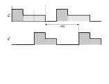
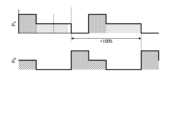
図5に示すタイミング図300は、ソース電力(ソースRF信号)PSとバイアス電力(バイアスRF信号)PBとを示す。ソース電力PSとは、ソースRF生成部31aからアンテナ(コイル)14に供給されるRF電力である。また、バイアス電力PBとは、バイアスRF生成部31bから基板支持部11a中の下部電極に供給されるRF電力である。ソースRF生成部31aは、たとえば、制御部から供給される制御信号に応じてソース電力PSを生成する。生成されたソース電力PSは、コイルに供給される。バイアスRF生成部31bは、たとえば、制御部から供給される制御信号に応じてバイアス電力PBを生成する。生成されたバイアス電力PBは、下部電極に供給される。 The timing diagram 300 shown in FIG. 5 shows source power (source RF signal) PS and bias power (bias RF signal) PB. The source power PS is RF power supplied from the source
図5中、周期100は、ソースRF信号の1周期を示す。以下、各周期1001、1002…を区別する必要がない場合、まとめて周期100と呼ぶ。周期200は、バイアスRF信号の1周期を示す。以下、各周期2001、2002、…を区別する必要がない場合、まとめて周期200と呼ぶ。1周期はパルス信号の立ち上がりから次の立ち上がりまでの期間、すなわち、オン期間とオフ期間を合計した期間を指す。ソースRF信号およびバイアスRF信号は、同一周波数のパルス信号である。 In Fig. 5,
ソースRF信号は、コイルにRF電力が供給される状態であるソースオン状態(第1状態:図5のPhase 1~Phase 3を参照)と、コイルにRF電力が供給されない状態であるソースオフ状態(第2状態:図5のPhase 4を参照)とを繰り返す。ソースRF信号がソースオン状態のとき、ソース電力PSがコイルに供給される。ソースRF信号がソースオフ状態のとき、コイルには電力は供給されない、すなわち、コイルへのRF電力の供給は停止される。各ソースオン状態は、少なくとも2つのソースパワーレベル(High/Low)を有する。図5に示す例では、ソースオン状態は、第1のソース期間(Phase 1)の間の第1のソースパワーレベル(High)と、前記第1のソース期間(Phase 1)の後の第2のソース期間(Phase 2,3)の間の第2のソースパワーレベル(Low)とを有する。つまり、図5の例においては、第1のソースパワーレベル(High)は、第2のソースパワーレベル(Low)よりも大きい。 The source RF signal repeats a source-on state (first state: see
バイアスRF信号は、下部電極にRF電力が供給される状態であるバイアスオン状態(第1状態:図5における期間D2を除くPhase 2~Phase 3を参照)と、下部電極にRF電力が供給されない状態であるオフ状態(第2状態;図5のPhase 4参照)とを繰り返す。図5の例では、バイアスRF信号がオン状態のとき、バイアス電力PBが下部電極に供給される。バイアスRF信号がオフ状態のとき、下部電極には電力は供給されない、すなわち、下部電極へのRF電力の供給は停止される。各バイアスオン状態は、少なくとも2つのバイアスパワーレベル(High/Low)を有する。図5に示す例では、バイアスオン状態は、第1のバイアス期間(期間D2を除くPhase 2)の間の第1のバイアスパワーレベル(High)と、前記第1のバイアス期間(期間D2を除くPhase 2)の後の第2のバイアス期間(Phase 3)の間の第2のバイアスパワーレベル(Low)とを有する。つまり、図5の例においては、第1のバイアスパワーレベル(High)は、第2のバイアスパワーレベル(Low)よりも大きい。 The bias RF signal alternates between a bias-on state (first state: see
図5において、バイアスRF信号の立ち上がり(タイミングtB1)は、ソースRF信号の立ち上がり(タイミングtS1)に対して期間D1だけ遅延している。つまり、ソースRF信号の周期100とバイアスRF信号の周期200とは、期間D1だけずれている。ソースRF信号がオン状態のハイレベル(図5中、H)からローレベル(図5中、L)に遷移(タイミングtS2)してから期間D2後にバイアスRF信号が立ち上がる。図5の例では、前のバイアスサイクルのバイアスオフ状態から第1のバイアスサイクル2001におけるバイアスオン状態(High)への遷移タイミングtB1は、第1のバイアスサイクルtB1に対応する第1のソースサイクルtS1におけるソースオン状態(High)への遷移タイミングtS1に対してずれている(遅延している)。また、バイアスRF信号は、第1のソース期間(Phase 1)の間にバイアスオフ期間を有する。 In Fig. 5, the rising edge of the bias RF signal (timingtB1 ) is delayed by a periodD1 from the rising edge of the source RF signal (timingtS1 ). That is, the
次に、ソースRF信号がローレベルを維持している間に、バイアスRF信号はハイレベルからローレベルに遷移する(タイミングtB2)。従って、第1のバイアス期間(期間D2を除くPhase 2)及び第2のバイアス期間(Phase 3)は、第2のソース期間(Phase 2,3)と部分的に重複している。また、バイアスRF信号は、第2のソース期間(Phase 2,3)の間に第1のバイアスパワーレベル(High)から第2のバイアスパワーレベル(Low)に遷移される、そして、ソースRF信号がローレベルからオフ状態に遷移するタイミング(タイミングtS3)と同時に、バイアスRF信号はオフ状態に遷移する(タイミングtB3)。従って、図5のPhase 4において、ソースオフ状態の期間は、バイアスオフ状態の期間と重複している。 Next, while the source RF signal maintains a low level, the bias RF signal transitions from a high level to a low level (timingtB2 ). Therefore, the first bias period (
ソースRF信号はオフ状態に遷移した後、タイミングtS4でオン状態に遷移し、次の周期1002が開始する。他方、バイアスRF信号は、タイミングtS4ではオフ状態を維持する。そして、ソースRF信号の立ち上がりから期間D1だけ遅延したタイミングtB4において、バイアスRF信号はオフ状態からオン状態に遷移する。 After the source RF signal transitions to the OFF state, it transitions to the ON state at timingtS4 , starting the next cycle1002. On the other hand, the bias RF signal maintains the OFF state at timingtS4 . Then, at timingtB4 , which is delayed by a periodD1 from the rising edge of the source RF signal, the bias RF signal transitions from the OFF state to the ON state.
このように、ソースRF信号が状態遷移するタイミングと、バイアスRF信号が状態遷移するタイミングとはずれている。図5の例では、ソースRF信号がハイレベルからローレベルに遷移するタイミングと、バイアスRF信号がオフ状態からオン状態に遷移するタイミングとは、期間D2だけずれている。また、ソースRF信号の状態とバイアスRF信号の状態とは非対称に遷移する。 In this way, the timing at which the source RF signal makes a state transition is offset from the timing at which the bias RF signal makes a state transition. In the example of Fig. 5, the timing at which the source RF signal makes a transition from a high level to a low level is offset from the timing at which the bias RF signal makes a transition from an off state to an on state by a periodD2 . In addition, the states of the source RF signal and the bias RF signal make asymmetric transitions.
また、ソースRF信号のオン期間(タイミングtS1からtS3まで)およびオフ期間(タイミングtS3からtS4まで)それぞれの長さは、バイアスRF信号のオン期間(タイミングtB1からtB3まで)およびオフ期間(タイミングtB3からtB4まで)それぞれの長さと異なる。図5の例では、ソースRF信号のデューティ比(1周期に対するオン期間の長さの割合)は、約75%である。また、バイアスRF信号のデューティ比は約40%である。ただし、ソースRF信号とバイアスRF信号が同一のデューティ比を有してもよい。また、ソースRF信号とバイアスRF信号のデューティ比は、約3%から約90%の範囲内でそれぞれ別個に設定可能である。ソースRF信号およびバイアスRF信号のデューティ比についてはさらに後述する。 Also, the lengths of the on-period (from timingtS1 totS3 ) and off-period (from timingtS3 totS4 ) of the source RF signal are different from the lengths of the on-period (from timingtB1 totB3 ) and off-period (from timingtB3 totB4 ) of the bias RF signal. In the example of FIG. 5, the duty ratio of the source RF signal (the ratio of the length of the on-period to one period) is about 75%. Also, the duty ratio of the bias RF signal is about 40%. However, the source RF signal and the bias RF signal may have the same duty ratio. Also, the duty ratios of the source RF signal and the bias RF signal can be set separately within the range of about 3% to about 90%. The duty ratios of the source RF signal and the bias RF signal will be described in more detail later.
ソース電力PSとバイアス電力PBの供給態様は、以下の4つのフェーズを推移する。 The supply of the source power PS and the bias power PB changes through the following four phases.
(1)第1フェーズ(図5中110、成膜モード):
第1フェーズ110は、パラメータセット{PS1,PB1,t1}により定義される。ここで、PS1は、第1フェーズ110中に供給されるソース電力PSの値である。PB1は、第1フェーズ110中に供給されるバイアス電力PBの値である。t1は、第1フェーズ110の期間の長さを示す。ここで、以下の関係が成立する。
PS1>0
PB1=0
t1>0 (1) First phase (110 in FIG. 5, film formation mode):
The
PS1 >0
PB1 =0
t1 >0
第1フェーズ110中は、ソース電力PSはハイレベルでコイルに供給されるが、バイアス電力PBは下部電極に供給されない。第1フェーズ110中は、プラズマ処理装置1の上部のみにRF電力が供給されてプラズマが生成され、プラズマ中にイオンおよびラジカルが生成される。バイアス電力PBも重畳して供給される場合と比較すると生成されるラジカルやイオンは少ないが、バイアス電力PBによる引き込み力がないため、基板上では主として成膜が進む。 During the
(2)第2フェーズ(図5中120、高選択性エッチングモード):
第2フェーズ120は、パラメータセット{PS2,PB2,t2}および{PS3,PB3,t3}により定義される。ここで、PS2は、第2フェーズ120中、期間D2の間に供給されるソース電力PSの値である。PB2は、第2フェーズ120中、期間D2の間に供給されるバイアス電力PBの値である。t2は、第2フェーズ120中、期間D2の長さを示す。D2は、第2フェーズ120開始からバイアス電力PBの供給が開始するまでの遅延期間の長さを示す。ここで、以下の関係が成立する。
PS1>PS2>0
PB2=0
t2=D2>0 (2) Second phase (120 in FIG. 5, high selectivity etching mode):
The
PS1 > PS2 >0
PB2 =0
t2 =D2 > 0
また、PS3は、第2フェーズ120中、期間D2を除いた期間中に供給されるソース電力PSの値である。PB3は、第2フェーズ120中、期間D2を除いた期間中に供給されるバイアス電力PBの値である。また、t3は、第2フェーズ120中、期間D2を除いた期間の長さを示す。ここで、以下の関係が成立する。
PS3=PS2>0
PB3>0
t3>0 Moreover, PS3 is the value of source power PS supplied during the period excluding periodD2 during the
PS3 = PS2 >0
PB3 >0
t3 >0
第2フェーズ120開始時(タイミングtS2)にソース電力PSのレベルがハイレベルからローレベルに切り替わる。また、第2フェーズ120が開始してから期間D2経過後(タイミングtB1)に、バイアス電力PBがオン状態(ハイレベル)に遷移する。期間D2は、エッチング生成物の排気時間に対応する。第2フェーズ120中は、バイアス電力PBが供給されることで、下部電極へのイオンの引き込み力(イオンエネルギー)が生じる。また、ソース電力PSの供給はローレベルに移行するが継続される。このため、高い選択性でのエッチングが進む。 At the start of the second phase 120 (timing tS2 ), the level of the source power PS switches from high to low. After a period D2 has elapsed since the start of the second phase 120 (timing tB1 ), the bias power PB transitions to the on state (high level). The period D2 corresponds to the exhaust time of the etching product. During the
(3)第3フェーズ(図5中130、マイルドエッチングモード):
第3フェーズ130は、パラメータセット{PS4,PB4,t4}により定義される。ここで、PS4は、第3フェーズ130中に供給されるソース電力PSの値である。PB4は、第3フェーズ130中に供給されるバイアス電力PBの値である。t4は、第3フェーズ130の期間の長さを示す。ここで以下の関係が成立する。
PS2=PS3=PS4
PB3>PB4>0
t4>0 (3) Third phase (130 in FIG. 5, mild etching mode):
The
PS2 = PS3 = PS4
PB3 > PB4 >0
t4 >0
第3フェーズ130開始時(タイミングtB2)に、バイアス電力PBはハイレベルからローレベルに切り替わる。他方、ソース電力PSはローレベルのまま維持される。このため、プラズマ処理空間10s中のラジカルおよびイオンの量は大きく減少しないが、基板へのイオンの引き込み力(イオンエネルギー)が減少する。このため、凹部OPの底部ではエッチングが抑制され、凹部OPの底部よりも頂部付近がエッチングされて、堆積物による開口閉塞が防止される。 At the start of the third phase 130 (timing tB2 ), the bias power PB is switched from high to low. On the other hand, the source power PS is maintained at low level. Therefore, the amount of radicals and ions in the
(4)第4フェーズ(図5中140、排気モード):
第4フェーズ140は、パラメータセット{PS5,PB5,t5}により定義される。ここで、PS5は、第4フェーズ140中に供給されるソース電力PSの値である。PB5は、第4フェーズ140中に供給されるバイアス電力PBの値である。t5は、第4フェーズ140の期間の長さを示す。ここで以下の関係が成立する。
PS5=PB5=0
t5>0 (4) Fourth phase (140 in FIG. 5, exhaust mode):
The
PS5 =PB5 =0
t5 >0
第4フェーズ140開始時(タイミングtS3,tB3)に、ソース電力PSおよびバイアス電力PBはともにオフ状態に遷移する。このため、プラズマ処理空間10s内でのプラズマの生成が停止し、ラジカル密度、イオン密度、イオンエネルギーがいずれも減少していく。このとき、排気システム40は動作を継続しているため、プラズマ処理空間10s内からラジカルや副生成物が徐々に排気されていく。 At the start of the fourth phase 140 (timingtS3 ,tB3 ), the source powerPs and the bias powerPb both transition to the OFF state. As a result, the generation of plasma in the
第4フェーズの後、再び第1フェーズに戻り、ソース電力PSが印加される。ソース電力PSの印加により、再びプラズマが生成される。 After the fourth phase, the process returns to the first phase and the
このように実施形態に係るプラズマ処理では、ソース電力PSとバイアス電力PBを異なるタイミングで状態遷移させる。また、ソース電力PSとバイアス電力PBは非対称な状態に遷移する。このため、実施形態に係るプラズマ処理装置1は、プラズマ処理空間10s内のプラズマの状態を、所望のプラズマ処理に適した状態に制御することができる。このため、プラズマ処理装置1は、効率的に基板上に所望形状のパターンを形成できる。プラズマ処理装置1は、たとえば図5のパルス波形を有するソースRF信号およびバイアスRF信号を用いることで、プラズマ処理空間10s内のイオン、ラジカルおよび副生成物の状態を制御しつつ垂直方向のエッチングを実現できる。このため、プラズマ処理装置1は、エッチングにより発生する形状異常を抑制してプラズマエッチングの処理性能を向上させることができる。 In this manner, in the plasma processing according to the embodiment, the source power P1 S and the
図5の例においては、以下の関係が成立する。
PS1>PS2=PS3=PS4>0
PB3>PB4>0
PB1=PB2=PB5=PS5=0
t1>0
t2=D2>0
t3>0
t4>0
t5>0
ただし、本実施形態は上記の関係が成立する場合だけでなく、他の関係においても適用できる。他の関係については変形例として後述する。 In the example of FIG. 5, the following relationships hold:
PS1 > PS2 = PS3 = PS4 >0
PB3 > PB4 >0
PB1 = PB2 = PB5 = PS5 =0
t1 >0
t2 =D2 > 0
t3 >0
t4 >0
t5 >0
However, this embodiment is not limited to the above relationship, and can be applied to other relationships as well, which will be described later as modified examples.
図6は、ソース電力PSおよびバイアス電力PBの値とプラズマの状態を示す物理量との関係について説明するための図である。 FIG. 6 is a diagram for explaining the relationship between the values of the source power PS and bias power PB and the physical quantities indicating the state of the plasma.
図6の(A)に示す波形例は、実験用に設定した波形例である。図6の波形例について、期間1~4に分けて説明する。期間1、2、3に対応して、ソース電力PSの値は、ハイレベル、ミドルレベル、ローレベルの順に遷移する。期間3と期間4の間はソース電力PSの値は変わらない。期間1~4に対応して、バイアス電力PBの値は、ハイレベル、ミドルレベル、ハイレベル、ローレベルの順に遷移する。 The waveform example shown in Fig. 6A is an example of a waveform set for an experiment. The waveform example in Fig. 6 will be explained by dividing it into
図6の(B)、(C)、(D)、(E)はそれぞれ、(A)の電力値の変化に対応する、プラズマ処理空間10s内のイオン密度Γi、ラジカル密度Γr、イオンエネルギーεiおよび副生成物密度Γbpの変化を示す。 6B, 6C, 6D, and 6E respectively show the changes in ion density Γi , radical density Γr , ion energy εi , and by-product density Γbp in the
誘導結合型、波励起型、ECR型の場合、反応種の生成量はソース電力PSと相関関係にあるといってよい。このため、プラズマ処理の開始時にまず反応種を生成する段階で、ソース電力PSを高いレベルに設定している。また、イオン密度Γiやラジカル密度Γrも、ソース電力PSの供給量が多い期間1において増加している。このため、期間1のように、ソース電力PSを高いレベルで供給することが、効率的な成膜やエッチングに効果的といえる。 In the case of the inductively coupled, wave excited and ECR types, the amount of reactive species generated can be said to be correlated with the source powerPs. For this reason, the source power Psis set to a high level at the stage where reactive species are first generated at the start of plasma processing. In addition, the ion densityΓi and the radical densityΓr also increase in
しかし、ソース電力PSを高いレベルで供給し続けると、副生成物密度Γbpも増加していく。Γbpは、ソース電力PSおよびバイアス電力PBをともにハイレベルからミドルレベルに下げた期間2において増加している。これは、バイアス電力PBが相対的に高くなったことで、増加したイオンエネルギーによりエッチングの効果が強くなり、エッチングにより生じる副生成物が増加したと考えられる。イオンエネルギーは、バイアス電力PBをハイレベルに戻した期間3においてスパイク状に増加している。期間3では、ソース電力PSはローレベルとなっているがラジカル密度Γrは大幅な減少は見られない。イオン密度Γiは徐々に減少している。そして、ソース電力PSおよびバイアス電力PBがともにローレベルとなる期間4では、ラジカル密度Γr以外の3つの物理量はいずれも減少し、0に近づく。特に、イオンエネルギーがεiと副生成物密度Γbpは大幅に減少する。 However, if the source power PS continues to be supplied at a high level, the by-product density Γbp also increases. Γbp increases in
期間1のように、ソース電力PSおよびバイアス電力PBを同時に高レベルで供給することで、ラジカルおよびイオンの量を迅速に増加させることができる。このため、プラズマ処理開始時にはソース電力PSおよびバイアス電力PBを高レベルに供給することが好ましいと考えられる。 The amount of radicals and ions can be increased rapidly by simultaneously supplying the source power P2 S and the
次に期間2のように、ソース電力PSのレベルを下げると、イオンは減少してもラジカルの量はさほど変化しない。他方、バイアス電力PBが相対的に高いレベルに維持されると、イオンエネルギーを増加させることができる。このため、バイアス電力PBのレベル制御によって、イオン入射角を調整して垂直方向のエッチングを効果的に実現できる。また、期間1中にバイアス電力PBのレベルを先に低くし、一定の遅延後にソース電力PSのレベルを下げていることは、イオンエネルギーや副生成物の量に影響していると考えられる。このため、ソース電力PSのレベルの切換タイミングを調整することで、副生成物の量やイオンエネルギーの変動を制御できると考えられる。また、バイアス電力PBのレベルを調整することでイオンエネルギーを制御でき、イオンとラジカルの比率を調整できると言える。このため、バイアス電力PBのレベル調整により、さらにエッチング角度を調整して効果的にパターンをエッチングすることが可能である。 Next, as in
また、期間3のように、バイアス電力PBをハイレベルに戻したときにスパイク状にイオンエネルギーが増加することは、エッチングの際のイオン入射角を基板表面に対して垂直に近づける。このため、バイアス電力PBのレベル調整は、パターン底部のエッチングを効果的に実現するためにも有用と言える。図6の波形例からは、相対的にソース電力PSをローレベルにし、バイアス電力PBをハイレベルにすることが、垂直にパターン側壁をエッチングするために有用と考えられる。期間3におけるスパイク状のイオンエネルギーの増加は、基板上の凹部OP底部のコーナーのエッチングに効果的といえる。 Moreover, as in
さらに、期間4のように、ソース電力PSおよびバイアス電力PBをともに低いレベルに設定すれば、副生成物を高速で排気できると考えられる。 Furthermore, if the source power PS and the bias power PB are both set to low levels, as in
また、図6の波形のうち、期間2,4のソース電力PSのレベル、期間2~4のバイアス電力PBのレベルを調整すれば、さらにパターン中エッチングが進む位置や角度を調整できると考えられる。 Moreover, it is believed that by adjusting the level of the source power PS in
図5の波形例では、第1フェーズ110においてソース電力PSをハイレベルで供給して反応種を生成した後に、第2フェーズ120でソース電力PSをローレベルに下げる。その段階でバイアス電力PBをハイレベルで供給することでイオンエネルギーを上げて相対的に基板への引き込み(バイアス)力を強くしてエッチングを進める。その後、第3フェーズでバイアス電力PBをローレベルに切換え、引き込み力を弱めてパターン頂部側をエッチングして閉塞を防ぐ。その後、ソース電力PSおよびバイアス電力PBの両方をオフ状態に移行させて開口等に滞留している副生成物を排気する。 In the waveform example of Fig. 5, after the source power PS is supplied at a high level in the
このように、ソース電力PSとバイアス電力PB各々のレベルを、形成するパターンの形状に合わせて組み合わせてシーケンス化することにより、多様なパターン形成に適したRF電力の供給が実現できる。 In this way, by combining and sequencing the levels of the source power PS and the bias power PB in accordance with the shape of the pattern to be formed, it is possible to realize the supply of RF power suitable for forming a variety of patterns.
図7は、実施形態に係るプラズマ処理に用いるRF信号の3レベル波形の他の例を説明するための図である。図7の波形例では、ソース電力PSおよびバイアス電力PBのレベルをそれぞれ、ローレベル、ハイレベル、オフ状態の順に遷移させる。ソース電力PSおよびバイアス電力PBがオフ状態からオン状態に遷移するタイミングは同一である。また、ソース電力PSがローレベルからハイレベルに遷移するタイミングは、バイアス電力PBがローレベルからハイレベルに遷移するタイミングから期間D3だけ遅延する。また、バイアス電力PBがハイレベルからオフ状態に遷移するタイミングは、ソース電力PSがハイレベルからオフ状態に遷移するタイミングから期間D4だけ遅延する。 7 is a diagram for explaining another example of a three-level waveform of an RF signal used in a plasma processing according to an embodiment. In the waveform example of FIG. 7, the levels of the source power PS and the bias power PB are transitioned in the order of low level, high level, and off state, respectively. The timing at which the source power PS and the bias power PB transition from the off state to the on state is the same. In addition, the timing at which the source power PS transitions from the low level to the high level is delayed by a period D3 from the timing at which the bias power PB transitions from the low level to the high level. In addition, the timing at which the bias power P Btransitions from the high level to the off state is delayed by a period D4 from the timing at which the source power PS transitions from the high level to the off state.
図7の波形例は、図5の波形例と同様、第1フェーズから第4フェーズまでの4つのフェーズを含む。The waveform example in Figure 7 includes four phases, from the first phase to the fourth phase, similar to the waveform example in Figure 5.
第1フェーズ110においては、ソース電力PSおよびバイアス電力PBがともにローレベルで供給される。このため、反応種が生成され、かつ、イオンエネルギーが生成されて引き込み力が生じる。バイアス電力PBはローレベルで供給されるため、パターン頂部付近が徐々にエッチングされる。このため、急速なエッチングにより生成物が開口を閉塞する等の異常が抑制される。 In the
バイアス電力PBは、第1フェーズ110が終了する前にローレベルからハイレベルに遷移する。このため、第2フェーズ120の開始前にイオンエネルギーが上昇する。そして、第2フェーズ120に入ると、ソース電力PSおよびバイアス電力PBがともにハイレベルとなり、エッチングが進む。 The
次に、第3フェーズ130が開始するとまず、ソース電力PSがオフ状態に遷移する。このため、バイアス電力PBのみがハイレベルで印加される状態となり、パターン底部がエッチングされて垂直方向にパターン形状が補正される。 Next, when the
次に、第4フェーズ140は、ソース電力PSおよびバイアス電力PBがともにオフ状態となる。このため、プラズマ処理空間10s内の副生成物等の排気が進む。そして、次の周期1002が開始するときまでに、エッチング効果の妨げとなる副生成物が排気される。 Next, in the
図7の例においては、各フェーズのパラメータセットの関係は以下のようになる。第1フェーズ110は、パラメータセット{PS1,PB1,t1}および{PS2,PB2,t2}により定義される。第2フェーズ120は、パラメータセット{PS3,PB3,t3}により定義される。第3フェーズ130は、パラメータセット{PS4,PB4,t4}および{PS5,PB5,t5}により定義される。第4フェーズ140は、パラメータセット{PS6,PB6,t6}により定義される。 In the example of Fig. 7, the relationship between the parameter sets of each phase is as follows: The
パラメータセットは各フェーズ中、ソース電力PSおよびバイアス電力PBが一定値の期間ごとに規定される。図7の例では、6つのパラメータセットが規定される。 A parameter set is defined for each period during which the source power PS and the bias power PB are constant during each phase. In the example of Fig. 7, six parameter sets are defined.
第1のパラメータセット{PS1,PB1,t1}は、第1フェーズ中、ソース電力PSがローレベル、バイアス電力PBがローレベルの期間に対応する。したがって、以下の関係が成立する。
PS1=PSL
PB1=PBL
t1>0 The first parameter set {PS1 , PB1 , t1 } corresponds to the period during which the source power PS is at a low level and the bias power PB is at a low level during the first phase.
PS1 = PSL
PB1 = PBL
t1 >0
第2のパラメータセット{PS2,PB2,t2}は、第1フェーズ中、ソース電力PSがローレベル、バイアス電力PBがハイレベルの期間に対応する。したがって、以下の関係が成立する。
PS2=PSL
PB2=PBH
t2=D3>0 The second parameter set {PS2 , PB2 , t2 } corresponds to the period during which the source power PS is at a low level and the bias power PB is at a high level during the first phase.
PS2 = PSL
PB2 = PBH
t2 =D3 > 0
第3のパラメータセット{PS3,PB3,t3}は、第2フェーズのソース電力PSがハイレベル、バイアス電力PBがハイレベルの期間に対応する。したがって、以下の関係が成立する。
PS3=PSH
PB3=PBH
t3>0 The third parameter set {PS3 , PB3 , t3 } corresponds to a period during which the source power PS is at a high level and the bias power PB is at a high level in the second phase.
PS3 = PSH
PB3 = PBH
t3 >0
第4のパラメータセット{PS4,PB4,t4}は、第3フェーズ中、ソース電力PSがオフ状態、バイアス電力PBがハイレベルの期間に対応する。したがって、以下の関係が成立する。
PS4=PSOFF
PB4=PBH
t4=D4>0 The fourth parameter set {PS4 , PB4 , t4 } corresponds to the period during which the source power PS is in the off state and the bias power PB is at a high level during the third phase.
PS4 = PSOFF
PB4 = PBH
t4 =D4 >0
第5のパラメータセット{PS5,PB5,t5}は、第3フェーズ中、ソース電力PSがオフ状態、バイアス電力PBがオフ状態の期間に対応する。したがって、以下の関係が成立する。
PS5=PSOFF
PB5=PBOFF
t5>0 The fifth parameter set {PS5 , PB5 , t5 } corresponds to the period during which the source power PS is off and the bias power PB is off during the third phase.
PS5 = PSOFF
PB5 = PBOFF
t5 >0
第6のパラメータセット{PS6,PB6,t6}は、第4フェーズ中、ソース電力PSがオフ状態、バイアス電力PBがオフ状態の期間に対応する。したがって、以下の関係が成立する。
PS6=PSOFF
PB6=PBOFF
t6>0 The sixth parameter set {PS6 , PB6 , t6 } corresponds to the period during which the source power PS is off and the bias power PB is off during the fourth phase.
PS6 = PSOFF
PB6 = PBOFF
t6 >0
まとめると、以下の関係が成立する。
PS3>PS1=PS2>0=PS4=PS5=PS6
PB2=PB3=PB4>PB1>0=PB5=PB6
このように、図7の例では、第1のバイアスサイクル(2001)におけるバイアスオフ状態への遷移タイミング(tB1)は、第1のバイアスサイクル(2001)に対応する第1のソースサイクル(1001)におけるソースオフ状態への遷移タイミング(tS1)に対してずらされる(遅延される)。 In summary, the following relationship holds:
PS3 > PS1 = PS2 >0= PS4 = PS5 = PS6
PB2 = PB3 = PB4 > PB1 >0 = PB5 = PB6
Thus, in the example of FIG. 7 , the transition timing (tB1 ) to the bias-off state in the first bias cycle (2001 ) is shifted (delayed) with respect to the transition timing (tS1 ) to the source-off state in the first source cycle (1001 ) corresponding to the first bias cycle (2001 ).
図8は、実施形態に係るプラズマ処理に用いるRF信号の4レベル波形の一例を説明するための図である。図8の波形例は、図5および図7の波形例とは異なり、ソース電力PSおよびバイアス電力PBがそれぞれ、4つのレベルに遷移する。4つのレベルは、オフ状態と、3つのオン状態すなわちハイレベル、ミドルレベルおよびローレベルを含む。ソース電力PSは1周期100中、ハイレベル、ミドルレベル、ローレベル、オフ状態の順に遷移する。他方、バイアス電力PBは1周期200中、ミドルレベル、ローレベル、ハイレベル、オフ状態の順に遷移する。図8に示す例では、ソースオン状態(110,120,130)は、第1のソース期間(110)の間の第1のソースパワーレベル(High)と、第2のソース期間(120)の間の第2のソースパワーレベル(Middle)と、第3のソース期間(130)の間の第3のソースパワーレベル(Low)とを有する。第1のソースパワーレベル(High)は、第3のソースパワーレベル(Low)よりも大きく、第2のソースパワーレベル(Middle)は、第1のソースパワーレベル(High)と第3のソースパワーレベル(Low)との間の大きさである。バイアスオン状態(150,160,170,180)は、第1のバイアス期間(150,160)の間の第1のバイアスパワーレベル(Middle)と、第2のバイアス期間(170)の間の第2のバイアスパワーレベル(Low)と、第3のバイアス期間(180)の間の第3のバイアスパワーレベル(High)とを有する。第3のバイアスパワーレベル(High)は、第2のバイアスパワーレベル(Low)よりも大きく、第1のソースパワーレベル(Middle)は、第2のソースパワーレベル(Low)と第3のソースパワーレベル(High)との間の大きさである。 8 is a diagram for explaining an example of a four-level waveform of an RF signal used in the plasma processing according to the embodiment. The waveform example of FIG. 8 is different from the waveform examples of FIG. 5 and FIG. 7 in that the source power PS and the bias power PB each transition to four levels. The four levels include an off state and three on states, namely, a high level, a middle level, and a low level. The source power PS transitions in the order of a high level, a middle level, a low level, and an off state during one
また、図8の例では、ソースRF信号の1周期100はソース電力PSとバイアス電力PBのレベルの組み合わせに応じて、第1フェーズ110、第2フェーズ120、第3フェーズ130、第4フェーズ140および第5フェーズ150の5つの期間に分けられる。 Also, in the example of FIG. 8, one
図8の例では、ソース電力PSがオフ状態からオン状態に遷移するタイミングは、バイアス電力PBがオフ状態からオン状態に遷移するタイミングに対して、期間D5だけ遅延する。逆にいうと、バイアスRF信号の立ち上がりは、ソースRF信号の立ち上がりに対して期間D6だけ遅延する。その他の状態遷移のタイミングは、ソース電力PSとバイアス電力PBとで一致している。 8, the timing at which the source power PS transitions from the off state to the on state is delayed by a periodD5 from the timing at which the bias power PB transitions from the off state to the on state. Conversely, the rising edge of the bias RF signal is delayed by a periodD6 from the rising edge of the source RF signal. The timing of other state transitions is the same for the source power PS and the bias power PB.
第1フェーズ110では、ソース電力PSがオフ状態からハイレベルに遷移する。バイアス電力PBはミドルレベルで供給される。第2フェーズ120に入ると、ソース電力PSはハイレベルからミドルレベルに遷移する。他方、バイアス電力PBは、ミドルレベルからローレベルに遷移する。次の第3フェーズ130に入ると、ソース電力PSはミドルレベルからローレベルに遷移する。他方、バイアス電力PBは、ローレベルからハイレベルに遷移する。そして、第4フェーズ140では、ソース電力PSおよびバイアス電力PBがともにオフ状態に遷移する。次の第5フェーズ150では、バイアス電力PBのみがオフ状態からミドルレベルに遷移し、ソース電力PSはオフ状態を維持する。 In the
第1フェーズ110では、ソース電力PSおよびバイアス電力PBがともに供給されてプラズマ処理空間10s中に反応種が生成される。このためエッチングが進む。 In the
第2フェーズ120では、ソース電力PSおよびバイアス電力PBがともに相対的に低いレベルに切り替わる。このため、生成される反応種の量が減少し、それに伴って生成される副生成物の量が減少する。 In the
第3フェーズ130では、ソース電力PSは減じられるのに対して、バイアス電力PBがハイレベルに切り替えられる。このため、図6の期間3と同様に、イオンエネルギーがスパイク状に増加し、パターン底部のコーナーがエッチングされる。このため、第3フェーズはパターン側壁を垂直にする役割を果たす。 In the
第4フェーズ140では、ソース電力PSおよびバイアス電力PBがともにオフ状態に遷移する。このため、プラズマ処理空間10s内の副生成物やラジカルが排気される。 In the
第5フェーズ150では、バイアス電力PBのみがミドルレベルで供給される。この時点では、プラズマ処理空間10s内にラジカルが残存しているため、イオンエネルギーの引き込み力によりエッチングが緩やかに進み開口閉塞が防止される。 In the
このように、図8の波形例によっても、図12に示したようなパターンの形状異常を抑制しつつエッチングを実現することができる。In this way, even with the waveform example of Figure 8, etching can be achieved while suppressing pattern shape abnormalities such as those shown in Figure 12.
図8の例においては、各フェーズのパラメータセットの関係は以下のようになる。第1フェーズ110は、パラメータセット{PS1,PB1,t1}により定義される。第2フェーズ120は、パラメータセット{PS2,PB2,t2}により定義される。第3フェーズ130は、パラメータセット{PS3,PB3,t3}により定義される。第4フェーズ140は、パラメータセット{PS4,PB4,t4}により定義される。第5フェーズ150は、パラメータセット{PS5,PB5,t5}により定義される。 In the example of Fig. 8, the relationship between the parameter sets of each phase is as follows: The
ここで、以下の関係が成立する。
PS1>PS2>PS3>0
PS4=PS5=0
PB3>PB1=PB5>PB2>0
PB4=0
t1>0
t2>0
t3>0
t4>0
t5=D5>0 Here, the following relationship holds:
PS1 > PS2 > PS3 >0
PS4 = PS5 =0
PB3 > PB1 = PB5 > PB2 >0
PB4 =0
t1 >0
t2 >0
t3 >0
t4 >0
t5 =D5 >0
(デューティ比)
ところで、ソースRF信号およびバイアスRF信号のオン状態のデューティ比は、約3%から90%の範囲で別個に設定可能である旨、説明した。(Duty ratio)
As described above, the duty ratios of the source RF signal and the bias RF signal in the on state can be set independently within the range of approximately 3% to 90%.
たとえば3レベル波形の場合、ソースRF信号のハイレベルでのオン状態のデューティ比は、約5%から約50%の範囲内で設定可能である。また、ソースRF信号のローレベルでのオン状態のデューティ比は、0%から約45%の範囲内で設定可能である。また、ソースRF信号のオフ状態のデューティ比は、約5%から約90%の範囲内で設定可能である。For example, in the case of a three-level waveform, the duty ratio of the on state of the source RF signal at a high level can be set within a range of approximately 5% to approximately 50%. The duty ratio of the on state of the source RF signal at a low level can be set within a range of approximately 0% to approximately 45%. The duty ratio of the off state of the source RF signal can be set within a range of approximately 5% to approximately 90%.
また、バイアスRF信号のハイレベルでのオン状態のデューティ比は、約5%から約50%の範囲内で設定可能である。また、バイアスRF信号のローレベルでのオン状態のデューティ比は、0%から約45%の範囲内で設定可能である。また、バイアスRF信号のオフ状態のデューティ比は、約5%から約90%の範囲内で設定可能である。The duty ratio of the bias RF signal in the on state at a high level can be set within a range of about 5% to about 50%. The duty ratio of the bias RF signal in the on state at a low level can be set within a range of about 0% to about 45%. The duty ratio of the bias RF signal in the off state can be set within a range of about 5% to about 90%.
また、ソースRF信号とバイアスRF信号とが同時にオフ状態となる期間の長さは、デューティ比約5%から約90%の範囲で設定可能である。この期間はたとえば、約0マイクロ秒から約500マイクロ秒の範囲内、さらに好ましくは、約10マイクロ秒から約50ミリ秒の範囲内で設定可能である。また、この期間は、ソースRF信号およびバイアスRF信号のデューティ比で約10%から約50%の範囲内に設定してもよい。The length of the period during which the source RF signal and the bias RF signal are simultaneously in the off state can be set in a duty ratio range of about 5% to about 90%. This period can be set, for example, in a range of about 0 microseconds to about 500 microseconds, and more preferably, in a range of about 10 microseconds to about 50 milliseconds. This period may also be set in a duty ratio range of about 10% to about 50% for the source RF signal and the bias RF signal.
(ソースRF信号とバイアスRF信号との間の遅延)
図5と図8の波形例では、ソースRF信号の立ち上がりとバイアスRF信号の立ち上がりとの間に遅延を設けた。遅延はたとえば、1周期に対して-100%から+100%までの範囲内で任意に設定可能である。ここで、-100%から+100%は、ソースRF信号の立下りからバイアスRF信号の立ち上がりまでを基準として設定する。図9A~図9Dは、実施形態のRF信号における遅延について説明するための図である。図9A~図9Dは、図5の波形例における遅延の設定例である。Delay between source RF signal and bias RF signal
In the waveform examples of Fig. 5 and Fig. 8, a delay is provided between the rising edge of the source RF signal and the rising edge of the bias RF signal. The delay can be set arbitrarily within the range of -100% to +100% for one period, for example. Here, -100% to +100% is set based on the time from the falling edge of the source RF signal to the rising edge of the bias RF signal. Figs. 9A to 9D are diagrams for explaining the delay in the RF signal of the embodiment. Figs. 9A to 9D are examples of delay settings in the waveform example of Fig. 5.
図9Aは、ソースRF信号の立ち下がりとバイアスRF信号の立ち上がりが一致している場合である。ここでは、このような場合を遅延0%と定義する。Figure 9A shows a case where the falling edge of the source RF signal and the rising edge of the bias RF signal coincide. Here, this case is defined as 0% delay.
図9Bは、ソースRF信号の立ち下がりとバイアスRF信号の立ち上がりが、ソースRF信号のオン状態分だけソース信号の立ち上がりより前にずれている場合である。ソースRF信号のオン状態のデューティ比をA%とすると、この場合の遅延は-A%である。Figure 9B shows a case where the falling edge of the source RF signal and the rising edge of the bias RF signal are shifted ahead of the rising edge of the source signal by the amount of time the source RF signal is on. If the duty ratio of the on state of the source RF signal is A%, then the delay in this case is -A%.
図9Cは、図9Bと同様、ソースRF信号の立ち下がりとバイアスRF信号の立ち上がりが、ソースRF信号のオン状態分だけずれている場合である。ただし、図9Cでは、ソースRF信号の立下りが先、バイアスRF信号の立ち上がりが後である。この場合の遅延は+A%である。Figure 9C shows a case where the falling edge of the source RF signal and the rising edge of the bias RF signal are shifted by the amount of time the source RF signal is on, similar to Figure 9B. However, in Figure 9C, the falling edge of the source RF signal comes first, and the rising edge of the bias RF signal comes later. The delay in this case is +A%.
図9Dは、ソースRF信号の立ち下りとバイアスRF信号の立ち上がりが、+100%遅延している場合である。すなわち、ソースRF信号の1周期分だけ、バイアスRF信号の立ち上がりがソースRF信号の立下りより後になっている。Figure 9D shows a case where the falling edge of the source RF signal and the rising edge of the bias RF signal are delayed by +100%. In other words, the rising edge of the bias RF signal is one period of the source RF signal later than the falling edge of the source RF signal.
これらの例から分かるように、ソースRF信号とバイアスRF信号を重畳させる態様は特に限定されない。As can be seen from these examples, the manner in which the source RF signal and the bias RF signal are superimposed is not particularly limited.
(RF電力供給の流れ)
図10は、実施形態に係るプラズマ処理のRF電力供給におけるパワーレベルの組み合わせシーケンスについて説明するための図である。(RF power supply flow)
FIG. 10 is a diagram for explaining a combination sequence of power levels in the RF power supply in the plasma processing according to the embodiment.
図10は、図5、図7および図8の波形例におけるパワーレベルの組み合わせシーケンスをまとめている。図10中、ハイレベル、ミドルレベル、ローレベル、オフ状態をそれぞれ、H,M,L,OFFと表示する。図10に示すように、図5の3レベル波形の場合、{PS,PB}は、{H,OFF}、{L,H}、{L,L}、{OFF,OFF}の順に推移する。図7の3レベル波形の場合、{PS,PB}は、{L,L}、{L,H}、{H,H}、{OFF,H}、{OFF,OFF}の順に推移する。また、図8の4レベル波形の場合、{PS,PB}は、{H,M}、{M,L}、{L,H}、{OFF,OFF}、{OFF,M}の順に推移する。 Fig. 10 summarizes the combination sequences of power levels in the waveform examples of Fig. 5, Fig. 7, and Fig. 8. In Fig. 10, the high level, middle level, low level, and off state are indicated as H, M, L, and OFF, respectively. As shown in Fig. 10, in the case of the three-level waveform of Fig. 5, {PS , PB } changes in the order of {H, OFF}, {L, H}, {L, L}, and {OFF, OFF}. In the case of the three-level waveform of Fig. 7, {PS , PB } changes in the order of {L, L}, {L, H}, {H, H}, {OFF, H}, and {OFF, OFF}. In addition, in the case of the four-level waveform of Fig. 8, {PS , PB } changes in the order of {H, M}, {M, L}, {L, H}, {OFF, OFF}, and {OFF, M}.
各波形に共通している点は以下の通りである。
(1)ソース電力PSおよびバイアス電力PBの双方がオフ状態の期間がある。
(2)ソース電力PSおよびバイアス電力PBがともにオン状態であり、かつレベルが異なる期間がある。
(3)ソース電力PSおよびバイアス電力PBのいずれか一方がオフ状態であり、他方がオン状態の期間がある。 The waveforms have the following in common:
(1) There is a period in which both the source power PS and the bias power PB are in the off state.
(2) There is a period in which the source power PS and the bias power PB are both in the on state but at different levels.
(3) There is a period during which either the source power P1 S or the
このように、本実施形態に係るプラズマ処理方法は、ソース電力PSとバイアス電力PBの供給態様、たとえば、各々のレベルの組み合わせを複数パターン設けている。このため、本実施形態に寄ればプラズマ処理の進行度合いに応じてプラズマ処理空間10s内のプラズマの状態を細かく制御してプラズマ処理を実行できる。このため、本実施形態によれば、基板上のパターン形状の異常を防止しつつプラズマエッチングを実現できる。 In this manner, the plasma processing method according to the present embodiment provides a plurality of patterns of combinations of the supply modes of the source power PS and the bias power PB , for example, the respective levels. Therefore, according to the present embodiment, the plasma processing can be performed by finely controlling the state of the plasma in the
図11は、実施形態に係るプラズマ処理のRF電力供給の流れの例を示すフローチャートである。図11に示すフロー1100はたとえば、図3のステップS32において実行される。FIG. 11 is a flow chart showing an example of the flow of RF power supply in plasma processing according to an embodiment.
まず、制御部の制御下で、RF電力供給部31は第1パラメータセット{PS1,PB1,t1}に規定されるRF電力供給を実行する(ステップS1110)。 First, under the control of the control unit, the RF
次に、制御部の制御下で、RF電力供給部31は第2パラメータセット{PS2,PB2,t2}により規定されるRF電力供給を実行する(ステップS1120)。 Next, under the control of the control unit, the RF
次に、制御部の制御下で、RF電力供給部31は第3パラメータセット{PS3,PB3,t3}により規定されるRF電力供給を実行する(ステップS1130)。 Next, under the control of the control unit, the RF
次に、制御部の制御下で、RF電力供給部31は第4パラメータセット{PS4,PB4,t4}により規定されるRF電力供給を実行する(ステップS1140)。 Next, under the control of the control unit, the RF
次に、制御部の制御下で、RF電力供給部31は第5パラメータセット{PS5,PB5,t5}により規定されるRF電力供給を実行する(ステップS1150)。 Next, under the control of the control unit, the RF
ステップS1110~S1150は1サイクルとして実行される。ステップS1150の後に続けてステップS1110に戻ってサイクルが再度実行されてもよい。Steps S1110 to S1150 are executed as one cycle. After step S1150, the process may return to step S1110 and the cycle may be executed again.
なお、上記第1~第5パラメータセットのうち、いずれか2つが同一であってもよい。この場合、図5の3レベル波形に基づくRF電力供給が実行できる。In addition, any two of the first to fifth parameter sets may be the same. In this case, RF power supply based on the three-level waveform in Figure 5 can be executed.
また、上記第1~第5のパラメータセットのうち、少なくとも一つのパラメータセットにおいて、{PSX,PBX}(ただしXは1から5の任意の整数)は{PSOFF,PBOFF}であってよい。この場合、図5,7,8の波形例のように、いずれかのフェーズにおいてソース電力PSおよびバイアス電力PBの供給を共に停止できる。 Furthermore, in at least one of the first to fifth parameter sets, {PSX , PBX } (where X is any integer from 1 to 5) may be {PSOFF , PBOFF }. In this case, the supply of both the source power PS and the bias power PB can be stopped in either phase, as in the waveform examples of FIGS.
また、上記第1~第5のパラメータセットのうち、少なくとも一つのパラメータセットにおいて、{PSY,PBY}(ただし、Y≠X、かつ、Yは1から5の整数)は{PSα,PBβ}であってよい。ただし、α≠β、かつ、αおよびβは、H,L,Mのいずれか一つである。この場合、図5,7,8の波形例のように、いずれかのフェーズにおいて、ソース電力PSとバイアス電力PBとを異なるレベルで供給できる。 Furthermore, in at least one of the first to fifth parameter sets, {PSY , PBY } (where Y ≠ X, and Y is an integer from 1 to 5) may be {PSα , PBβ }, where α ≠ β, and α and β are any one of H, L, and M. In this case, as in the waveform examples of FIGS. 5, 7, and 8, in any phase, the source power PS and the bias power PB can be supplied at different levels.
また、上記第1~第5のパラメータセットのうち、少なくとも一つのパラメータセットにおいて、{PSZ,PBZ}(ただし、Z≠X、Z≠Y、かつ、Zは1から5の整数)は{PSγ,PBδ}(ただし{γ,δ}≠{α,β})、であってよい。ただし、γおよびδのうち一方がOFF、他方がH,L,Mのいずれか一つである。この場合、図5,7,8の波形例のように、いずれかのフェーズにおいて、ソース電力PSおよびバイアス電力PBの一方の供給を停止して他方の供給を実行できる。 Furthermore, in at least one of the first to fifth parameter sets, {PSZ , PBZ } (where Z ≠ X, Z ≠ Y, and Z is an integer from 1 to 5) may be {PSγ , PBδ } (where {γ, δ} ≠ {α, β}), where one of γ and δ is OFF and the other is one of H, L, and M. In this case, as in the waveform examples of FIGS. 5, 7, and 8, in any phase, the supply of one of the source power PS and bias power PB can be stopped and the supply of the other can be started.
なお、上記の実施形態および変形例の一部は適宜変更してもよい。以下に考えられる変形態様を記載する。Note that some of the above embodiments and variations may be modified as appropriate. Possible variations are described below.
(他の実施形態)
ソース電力PSは、交流(AC)電力であってもよい。また、ソース電力PSは、RF電力であっても、VHF(Very High Frequency)電力であってもよい。ソース電力PSはたとえば、約60MHzから約200MHzの範囲内のRF電力であってもよい。また、ソース電力PSはたとえば、約25MHzから約60MHzの範囲内のRF電力であってもよい。ソース電力PSはたとえば、27MHzであってもよい。本実施形態において、ソース電力PSは、誘導結合型プラズマ(ICP)を生成する。ソース電力PSはたとえば、ヘリカルアンテナと結合してプラズマを生成する。Other Embodiments
The source powerPS may be an alternating current (AC) power. The source powerPS may be an RF power or a very high frequency (VHF) power. The source powerPS may be, for example, an RF power in a range of about 60 MHz to about 200 MHz. The source powerPS may be, for example, an RF power in a range of about 25 MHz to about 60 MHz. The source powerPS may be, for example, 27 MHz. In this embodiment, the source powerPS generates an inductively coupled plasma (ICP). The source powerPS is, for example, coupled with a helical antenna to generate the plasma.
バイアス電力PBは、交流(AC)電力であってもよい。また、バイアス電力PBは、直流(DC)パルス電力であってもよい。バイアス電力PBは、RF電力、HF(High Frequency)電力、MF(Medium Frequency)電力のいずれかであってもよい。バイアス電力PBはたとえば、約200kHzから約600kHzの範囲内の周波数の電力であってよい。バイアス電力PBはたとえば400kHzであってもよい。また、バイアス電力PBはたとえば、約600kHzから約13MHzの範囲内の電力であってもよい。 The bias power PB may be an alternating current (AC) power. Also, the bias power PB may be a direct current (DC) pulse power. The bias power PB may be any of an RF power, an HF (High Frequency) power, and an MF (Medium Frequency) power. For example, the bias power PB may be a power having a frequency in a range of about 200 kHz to about 600 kHz. For example, the bias power PB may be 400 kHz. Also, the bias power P Bmay be a power in a range of about 600 kHz to about 13 MHz.
ソース電力PSおよびバイアス電力PBは各々、各周期において、単一パルスとして、または連続パルスとして印加されてよい。たとえば、第1フェーズにおいて、期間t1に印加されるソース電力PS1は単一パルスであってもよく、連続パルスであってもよい。同様に、期間t3に印加されるバイアス電力PB3は単一パルスであってもよく、連続パルスであってもよい。 The source power PS and the bias power PB may each be applied as a single pulse or as a continuous pulse in each period. For example, in the first phase, the source power PS1 applied during the period t1 may be a single pulse or a continuous pulse. Similarly, the bias power PB3 applied during the period t3 may be a single pulse or a continuous pulse.
プラズマ処理チャンバ10には、予め定められたプラズマ処理に応じて選択される流量で、ガスが供給される。1周期中、実質的に同一の流量でガスがプラズマ処理チャンバ10に供給される。供給されるガスはたとえば、臭化水素(HBr)を含む。また、供給されるガスはたとえば、ヘリウム(He)やアルゴン(Ar)等の希ガスを含む。また、供給されるガスはたとえば、酸素(O2)、テトラフルオロメタン(CF4)、三フッ化窒素(NF3)、六フッ化硫黄(SF6)、塩素(Cl2)、テトラクロロメタン(CCl4)等を含んでもよい。 Gas is supplied to the
実施形態に係るプラズマ処理中に生成される副生成物は、プラズマ処理チャンバ10内のガスおよび基板の組成物に含まれる1以上の種の元素を含む化合物であってよい。たとえば、シリコン基板とHBrガスを用いる場合は、SiBrxを含有する副生成物が形成されうる。他にフッ化シリコン(SiFx)、塩化シリコン(SiClx)等のシリコン含有残渣や、(フォトレジスト、有機膜、プリカーサを用いた処理の場合には)フルオロカーボン(CFx)、ハイロドフルオロカーボン(CHxFy)等の炭素含有残渣なども副生成物として形成されうる。By-products generated during plasma processing according to embodiments may be compounds containing one or more elements contained in the composition of the gas and substrate in the
実施形態においてエッチングの対象とする膜およびエッチングに用いるマスクの材料は特に限定されない。たとえば、下地層L1(図4参照)はシリコンウエハであってよい。エッチング対象層L2は、誘電体膜たとえばシリコン含有誘電体膜であってもよい。エッチング対象層L2は複数種類の膜を積層して形成されてもよい。たとえば、エッチング対象層L2は、シリコン酸化膜とシリコン窒化膜が順次積層された層であってもよい。エッチング対象層L2は、シリコン酸化膜とポリシリコン膜が順次積層された層であってもよい。マスクMLは、カーボン含有膜であってよい。カーボン含有膜はアモルファスカーボン層(ACL)、スピンオンカーボン膜(SOC)で形成されてもよい。またはマスクMKは金属膜で形成されてもよい。また、図4には図示しないが、マスクMKの上にマスクMKと同様の開口パターンが形成されたシリコン酸窒化膜(SiON)や裏面反射防止膜(BARC)が存在してもよい。In the embodiment, the film to be etched and the material of the mask used for etching are not particularly limited. For example, the base layer L1 (see FIG. 4) may be a silicon wafer. The layer to be etched L2 may be a dielectric film, such as a silicon-containing dielectric film. The layer to be etched L2 may be formed by stacking a plurality of types of films. For example, the layer to be etched L2 may be a layer in which a silicon oxide film and a silicon nitride film are stacked in sequence. The layer to be etched L2 may be a layer in which a silicon oxide film and a polysilicon film are stacked in sequence. The mask ML may be a carbon-containing film. The carbon-containing film may be formed of an amorphous carbon layer (ACL) or a spin-on carbon film (SOC). Alternatively, the mask MK may be formed of a metal film. Although not shown in FIG. 4, a silicon oxynitride film (SiON) or a back surface anti-reflective coating (BARC) having an opening pattern similar to that of the mask MK may be present on the mask MK.
実施形態に係るプラズマ処理方法において、エッチング対象層L2がシリコン含有誘電体膜である場合は、マスクMKはACL、SOC等のカーボン含有膜であってよい。また、エッチング対象層L2がポリシリコン膜である場合はマスクMKはTEOS(テトラエトキシシラン)を用いて形成したシリコン酸化膜等であってよい。In the plasma processing method according to the embodiment, when the etching target layer L2 is a silicon-containing dielectric film, the mask MK may be a carbon-containing film such as ACL or SOC. When the etching target layer L2 is a polysilicon film, the mask MK may be a silicon oxide film formed using TEOS (tetraethoxysilane).
実施形態において、ソースRF生成部31aおよびバイアスRF生成部31bはそれぞれ複数個配置されてもよい。この場合、各ソースRF生成部31aは予め定められたタイミングで予め定められた一定量のパワーをコイルに供給してもよい。同様に、各バイアスRF生成部31bは予め定められたタイミングで予め定められた一定量のパワーを下部電極に供給してもよい。In an embodiment, a plurality of source
実施形態に係るRF信号のパルスシーケンスは、基板上に形成するパターン形状に応じてユーザが自由にプラズマ処理装置1上に設定して実行させることができる。たとえば、ユーザは、記憶部に格納された複数パターンの一つを選択して実行させたり、記憶部に新しいシーケンスのパターンを記憶させたりすることができる。The RF signal pulse sequence according to the embodiment can be freely set and executed on the
(実施形態の効果)
上記のように実施形態に係るプラズマ処理装置は、プラズマ処理チャンバと、少なくとも一つのコイルと、基板支持部と、ソースRF生成部と、バイアスRF生成部と、を備える。少なくとも一つのコイルは、プラズマ処理チャンバの上方に配置される。基板支持部は、プラズマ処理チャンバ内に配置され、下部電極を有する。ソースRF生成部は、ソースRF信号を少なくとも一つのコイルに供給するように構成される。ソースRF信号は、複数のソースサイクルを含み、各ソースサイクルは、ソースオン状態及びソースオフ状態を含む。ソースオン状態は、少なくとも2つのソースパワーレベルを有する。バイアスRF生成部は、バイアスRF信号を下部電極に供給するように構成される。バイアスRF信号は、複数のソースサイクルにそれぞれ対応する複数のバイアスサイクルを含む。各バイアスサイクルは、バイアスオン状態及びバイアスオフ状態を含む。バイアスオン状態は、少なくとも2つのバイアスパワーレベルを有する。第1のバイアスサイクルにおけるバイアスオン状態への遷移タイミングは、第1のバイアスサイクルに対応する第1のソースサイクルにおけるソースオン状態への遷移タイミングに対してずらされる。このように、プラズマ処理装置は、コイルおよび下部電極に供給するRF電力を異なるタイミングで変化させることができる。また、プラズマ処理装置は、コイルおよび下部電極に供給するRF電力を異なる状態に遷移させることができる。このため、プラズマ処理により形成するパターンの形状に応じて、プラズマ処理チャンバ内に生成されるプラズマの状態を細かく制御できる。このため、プラズマ処理装置は、プラズマエッチングの処理性能を向上させることができる。(Effects of the embodiment)
As described above, the plasma processing apparatus according to the embodiment includes a plasma processing chamber, at least one coil, a substrate support, a source RF generator, and a bias RF generator. The at least one coil is disposed above the plasma processing chamber. The substrate support is disposed in the plasma processing chamber and has a lower electrode. The source RF generator is configured to supply a source RF signal to the at least one coil. The source RF signal includes a plurality of source cycles, each of which includes a source-on state and a source-off state. The source-on state has at least two source power levels. The bias RF generator is configured to supply a bias RF signal to the lower electrode. The bias RF signal includes a plurality of bias cycles corresponding to the plurality of source cycles, each of which includes a bias-on state and a bias-off state. The bias-on state has at least two bias power levels. The transition timing to the bias-on state in a first bias cycle is shifted with respect to the transition timing to the source-on state in a first source cycle corresponding to the first bias cycle. In this manner, the plasma processing apparatus can change the RF power supplied to the coil and the lower electrode at different timings. In addition, the plasma processing apparatus can transition the RF power supplied to the coil and the lower electrode between different states. This allows the state of the plasma generated in the plasma processing chamber to be precisely controlled according to the shape of the pattern to be formed by the plasma processing. This allows the plasma processing apparatus to improve the processing performance of plasma etching.
また、実施形態に係るプラズマ処理装置において、バイアスオン状態への遷移タイミングは、ソースオン状態への遷移タイミングに対して遅延されてもよい。In addition, in the plasma processing apparatus according to the embodiment, the timing of the transition to the bias-on state may be delayed with respect to the timing of the transition to the source-on state.
また、実施形態に係るプラズマ処理装置において、第1のバイアスサイクルにおけるバイアスオフ状態への遷移タイミングは、第1のソースサイクルにおけるソースオフ状態への遷移タイミングと実質的に同じであってもよい。In addition, in the plasma processing apparatus according to the embodiment, the transition timing to the bias off state in the first bias cycle may be substantially the same as the transition timing to the source off state in the first source cycle.
また、実施形態に係るプラズマ処理装置は、プラズマ処理チャンバと、少なくとも一つのコイルと、基板支持部と、ソースRF生成部と、バイアスRF生成部と、を備えてもよい。少なくとも一つのコイルは、プラズマ処理チャンバの上方に配置される。基板支持部は、プラズマ処理チャンバ内に配置され、下部電極を有する。ソースRF生成部は、ソースRF信号を前記少なくとも一つのコイルに供給するように構成される。ソースRF信号は、複数のソースサイクルを含む。各ソースサイクルは、ソースオン状態及びソースオフ状態を含む。ソースオン状態は、少なくとも2つのソースパワーレベルを有する。バイアスRF生成部は、バイアスRF信号を下部電極に供給するように構成される。バイアスRF信号は、複数のソースサイクルにそれぞれ対応する複数のバイアスサイクルを含む。バイアスサイクルは、バイアスオン状態及びバイアスオフ状態を含む。バイアスオン状態は、少なくとも2つのバイアスパワーレベルを有する。第1のバイアスサイクルにおけるバイアスオフ状態への遷移タイミングは、第1のバイアスサイクルに対応する第1のソースサイクルにおけるソースオフ状態への遷移タイミングに対してずらされる。In addition, the plasma processing apparatus according to the embodiment may include a plasma processing chamber, at least one coil, a substrate support, a source RF generating unit, and a bias RF generating unit. The at least one coil is disposed above the plasma processing chamber. The substrate support is disposed in the plasma processing chamber and has a lower electrode. The source RF generating unit is configured to supply a source RF signal to the at least one coil. The source RF signal includes a plurality of source cycles. Each source cycle includes a source on state and a source off state. The source on state has at least two source power levels. The bias RF generating unit is configured to supply a bias RF signal to the lower electrode. The bias RF signal includes a plurality of bias cycles corresponding to the plurality of source cycles, respectively. The bias cycle includes a bias on state and a bias off state. The bias on state has at least two bias power levels. The transition timing to the bias off state in the first bias cycle is shifted with respect to the transition timing to the source off state in the first source cycle corresponding to the first bias cycle.
また、実施形態に係るプラズマ処理装置において、バイアスオフ状態への遷移タイミングは、ソースオフ状態への遷移タイミングに対して遅延されてもよい。In addition, in the plasma processing apparatus according to the embodiment, the timing of the transition to the bias-off state may be delayed with respect to the timing of the transition to the source-off state.
また、実施形態に係るプラズマ処理装置において、第1バイアスサイクルにおけるバイアスオン状態への遷移タイミングは、第1ソースサイクルにおけるソースオン状態への遷移タイミングと実質的に同じであってもよい。In addition, in the plasma processing apparatus according to the embodiment, the transition timing to the bias-on state in the first bias cycle may be substantially the same as the transition timing to the source-on state in the first source cycle.
また、実施形態に係るプラズマ処理装置において、前記ソースオフ状態の期間は、前記バイアスオフ状態の期間と部分的に重複してもよい。In addition, in the plasma processing apparatus according to the embodiment, the period of the source-off state may partially overlap with the period of the bias-off state.
また、実施形態に係るプラズマ処理装置において、ソースオン状態は、第1のソース期間の間の第1のソースパワーレベルと、第1のソース期間の後の第2のソース期間の間の第2のソースパワーレベルとを有してもよい。また、第1のソースパワーレベルは、第2のソースパワーレベルよりも大きくてもよい。In addition, in the plasma processing apparatus according to the embodiment, the source-on state may have a first source power level during the first source period and a second source power level during a second source period following the first source period. The first source power level may be greater than the second source power level.
また、実施形態に係るプラズマ処理装置において、バイアスオン状態は、第1のバイアス期間の間の第1のバイアスパワーレベルと、第1のバイアス期間の後の第2のバイアス期間の間の第2のバイアスパワーレベルとを有してもよい。また、第1のバイアスパワーレベルは、前記第2のバイアスパワーレベルよりも大きくてもよい。In addition, in the plasma processing apparatus according to the embodiment, the bias-on state may have a first bias power level during a first bias period and a second bias power level during a second bias period following the first bias period. The first bias power level may be greater than the second bias power level.
また、実施形態に係るプラズマ処理装置において、バイアスRF信号は、第1のソース期間の間にバイアスオフ期間を有してもよい。In addition, in the plasma processing apparatus according to the embodiment, the bias RF signal may have a bias off period during the first source period.
また、実施形態に係るプラズマ処理装置において、第1のバイアス期間及び第2のバイアス期間は、第2のソース期間と部分的に重複してもよい。また、バイアスRF信号は、第2のソース期間の間に第1のバイアスパワーレベルから第2のバイアスパワーレベルに遷移されてもよい。In addition, in the plasma processing apparatus according to the embodiment, the first bias period and the second bias period may partially overlap with the second source period. Also, the bias RF signal may transition from the first bias power level to the second bias power level during the second source period.
また、実施形態に係るプラズマ処理装置において、ソースオン状態は、第1のソース期間の間の第1のソースパワーレベルと、第1のソース期間の後の第2のソース期間の間の第2のソースパワーレベルとを有してもよい。また、第2のソースパワーレベルは、第1のソースパワーレベルよりも大きくてもよい。In addition, in the plasma processing apparatus according to the embodiment, the source-on state may have a first source power level during the first source period and a second source power level during a second source period following the first source period. The second source power level may be greater than the first source power level.
また、実施形態に係るプラズマ処理装置において、バイアスオン状態は、第1のバイアス期間の間の第1のバイアスパワーレベルと、第1のバイアス期間の後の第2のバイアス期間の間の第2のバイアスパワーレベルとを有してもよい。また、第2のバイアスパワーレベルは、第1のバイアスパワーレベルよりも大きくてもよい。In addition, in the plasma processing apparatus according to the embodiment, the bias-on state may have a first bias power level during the first bias period and a second bias power level during a second bias period following the first bias period. The second bias power level may be greater than the first bias power level.
また、実施形態に係るプラズマ処理装置において、ソースオン状態は、第1のソース期間の間の第1のソースパワーレベルと、第1のソース期間の後の第2のソース期間の間の第2のソースパワーレベルと、第2のソース期間の後の第3のソース期間の間の第3のソースパワーレベルとを有してもよい。第1のソースパワーレベルは、第3のソースパワーレベルよりも大きくてもよい。また、第2のソースパワーレベルは、第1のソースパワーレベルと第3のソースパワーレベルとの間の大きさであってもよい。バイアスオン状態は、第1のバイアス期間の間の第1のバイアスパワーレベルと、第1のバイアス期間の後の第2のバイアス期間の間の第2のバイアスパワーレベルと、第2のバイアス期間の後の第3のバイアス期間の間の第3のバイアスパワーレベルとを有してもよい。第3のバイアスパワーレベルは、第2のバイアスパワーレベルよりも大きくてもよい。第1のソースパワーレベルは、第2のソースパワーレベルと第3のソースパワーレベルとの間の大きさであってもよい。In the plasma processing apparatus according to the embodiment, the source-on state may have a first source power level during the first source period, a second source power level during the second source period after the first source period, and a third source power level during the third source period after the second source period. The first source power level may be greater than the third source power level. The second source power level may have a magnitude between the first source power level and the third source power level. The bias-on state may have a first bias power level during the first bias period, a second bias power level during the second bias period after the first bias period, and a third bias power level during the third bias period after the second bias period. The third bias power level may be greater than the second bias power level. The first source power level may have a magnitude between the second source power level and the third source power level.
今回開示された実施形態は全ての点で例示であって制限的なものではないと考えられるべきである。上記の実施形態は、添付の請求の範囲およびその趣旨を逸脱することなく、様々な形態で省略、置換、変更されてもよい。The embodiments disclosed herein should be considered in all respects as illustrative and not restrictive. The above-described embodiments may be omitted, substituted, or modified in various ways without departing from the scope and spirit of the appended claims.
例えば、上記実施形態では、誘導結合型プラズマ装置を例に説明したが、これに限定されるものではなく、他のプラズマ装置に適用されてもよい。例えば、誘導結合型プラズマ装置に代えて、容量結合型プラズマ(Capacitively-coupled plasma:CCP)装置が用いられてもよい。この場合、容量結合型プラズマ装置は、プラズマ処理チャンバ内に配置される2つの対向する電極を含む。一実施形態において、一方の電極は、基板支持部内に配置され、他方の電極は、基板支持部の上方に配置される。この場合、一方の電極は下部電極として機能し、他方の電極は上部電極として機能する。そして、ソースRF生成部31a及びバイアスRF生成部31bは、2つの対向する電極のうち少なくとも1つに結合される。一実施形態において、ソースRF生成部31aは、上部電極に結合され、バイアスRF生成部31bは、下部電極に結合される。なお、ソースRF生成部31a及びバイアスRF生成部31bが下部電極に結合されてもよい。For example, in the above embodiment, an inductively coupled plasma device is described as an example, but the present invention is not limited thereto and may be applied to other plasma devices. For example, instead of the inductively coupled plasma device, a capacitively coupled plasma (CCP) device may be used. In this case, the capacitively coupled plasma device includes two opposing electrodes arranged in a plasma processing chamber. In one embodiment, one electrode is arranged in a substrate support, and the other electrode is arranged above the substrate support. In this case, one electrode functions as a lower electrode, and the other electrode functions as an upper electrode. Then, the source
1 プラズマ処理装置
10 プラズマ処理チャンバ
10a 誘電体窓
10b 側壁
10s プラズマ処理空間
11 支持部
11a 基板支持部
11b エッジリング支持部
12 エッジリング
13 ガス導入部
13a 中央ガス注入部
13b 側壁ガス注入部
14 アンテナ
20 ガス供給部
21 ガスソース
22 流量制御器
30 電力供給部
31 RF電力供給部
31a ソースRF生成部
31b バイアスRF生成部
32 DC電力供給部
40 排気システム
W 基板REFERENCE SIGNS
Claims (10)
Translated fromJapanese前記プラズマ処理チャンバ内に配置される基板支持部と、
前記プラズマ処理チャンバに結合され、ソースRF信号を生成するように構成されるソースRF生成部であり、前記ソースRF信号は、各サイクルにおける第1の期間にゼロパワーレベルより大きい第1のソースパワーレベルを有し、各サイクルにおける前記第1の期間に続く第2の期間に前記第1のソースパワーレベルとは異なりゼロパワーレベルより大きい第2のソースパワーレベルを有し、各サイクルにおける前記第2の期間に続く第3の期間に前記第2のソースパワーレベルを有し、各サイクルにおける前記第3の期間に続く第4の期間にゼロパワーレベルを有する、ソースRF生成部と、
前記基板支持部に結合され、バイアスRF信号を生成するように構成されるバイアスRF生成部であり、前記バイアスRF信号は、前記第1の期間にゼロパワーレベルを有し、前記第2の期間における遅延時間にゼロパワーレベルを有し、前記遅延時間を除く前記第2の期間にゼロパワーレベルより大きい第1のバイアスパワーレベルを有し、前記第3の期間に前記第1のバイアスパワーレベルとは異なりゼロパワーレベルより大きい第2のバイアスパワーレベルを有し、前記第4の期間にゼロパワーレベルを有する、バイアスRF生成部と、
を備える、プラズマ処理装置。 a plasma processing chamber;
a substrate support disposed within the plasma processing chamber;
a source RF generator coupled to the plasma processing chamber and configured to generate a source RF signal, the source RF signalhaving a first source power level greater than a zero power level during a first time period in each cycle, a second source power level different from the first source power level and greater than the zero power level during a second time period following the first time period in each cycle, the second source power level during a third time period following the second time period in each cycle, and a zero power level during a fourth time period following the third time period in each cycle ;
a bias RF generating unit coupled to the substrate support and configured to generate a bias RF signal, the bias RF signalhaving a zero power level in the first time period, a zero power level at a delay time in the second time period, a first bias power level greater than the zero power level in the second time period excluding the delay time, a second bias power level different from the first bias power level and greater than the zero power level in the third time period, and a zero power level in the fourth time period ;
A plasma processing apparatus comprising:
前記プラズマ処理チャンバ内に配置される基板支持部と、a substrate support disposed within the plasma processing chamber;
前記プラズマ処理チャンバに結合され、ソースRF信号を生成するように構成されるソースRF生成部であり、前記ソースRF信号は、各サイクルにおける第1の期間にゼロパワーレベルより大きい第1のソースパワーレベルを有し、各サイクルにおける前記第1の期間に続く第2の期間に前記第1のソースパワーレベルとは異なりゼロパワーレベルより大きい第2のソースパワーレベルを有し、各サイクルにおける前記第2の期間に続く第3の期間にゼロパワーレベルを有する、ソースRF生成部と、a source RF generator coupled to the plasma processing chamber and configured to generate a source RF signal, the source RF signal having a first source power level greater than a zero power level during a first time period in each cycle, a second source power level different from the first source power level and greater than the zero power level during a second time period following the first time period in each cycle, and a zero power level during a third time period following the second time period in each cycle;
前記基板支持部に結合され、バイアスRF信号を生成するように構成されるバイアスRF生成部であり、前記バイアスRF信号は、前記第1の期間における第1の時間にゼロパワーレベルより大きい第1のバイアスパワーレベルを有し、前記第1の期間における前記第1の時間に続く第2の時間に前記第1のバイアスパワーレベルとは異なりゼロパワーレベルより大きい第2のバイアスパワーレベルを有し、前記第2の期間に前記第2のバイアスパワーレベルを有し、前記第3の期間における前記第2の期間に続く第3の時間に前記第2のバイアスパワーレベルを有し、前記第3の期間における前記第3の時間に続く第4の時間にゼロパワーレベルを有する、バイアスRF生成部とを備える、a bias RF generator coupled to the substrate support and configured to generate a bias RF signal, the bias RF signal having a first bias power level greater than a zero power level at a first time in the first time period, a second bias power level different from the first bias power level and greater than a zero power level at a second time subsequent to the first time in the first time period, the second bias power level at the second time period, the second bias power level at a third time subsequent to the second time period in the third time period, and a zero power level at a fourth time subsequent to the third time in the third time period.
プラズマ処理装置。Plasma processing equipment.
前記バイアスRF信号は、前記第4の期間にゼロパワーレベルを有する、請求項4~6のうちいずれか一項に記載のプラズマ処理装置。7. The plasma processing apparatus of claim 4, wherein the bias RF signal has a zero power level during the fourth period.
前記プラズマ処理チャンバ内に配置される基板支持部と、a substrate support disposed within the plasma processing chamber;
前記プラズマ処理チャンバに結合され、ソースRF信号を生成するように構成されるソースRF生成部であり、前記ソースRF信号は、各サイクルにおける第1の期間にゼロパワーレベルより大きい第1のソースパワーレベルを有し、各サイクルにおける前記第1の期間に続く第2の期間に前記第1のソースパワーレベルとは異なりゼロパワーレベルより大きい第2のソースパワーレベルを有し、各サイクルにおける前記第2の期間に続く第3の期間に前記第1のソースパワーレベル及び前記第2のソースパワーレベルとは異なりゼロパワーレベルより大きい第3のソースパワーレベルを有し、各サイクルにおける前記第3の期間に続く第4の期間にゼロパワーレベルを有し、各サイクルにおける前記第4の期間に続く第5の期間にゼロパワーレベルを有する、ソースRF生成部と、a source RF generator coupled to the plasma processing chamber and configured to generate a source RF signal, the source RF signal having a first source power level during a first period in each cycle that is greater than a zero power level, a second source power level during a second period following the first period in each cycle that is different from the first source power level and greater than the zero power level, a third source power level during a third period following the second period in each cycle that is different from the first source power level and the second source power level and greater than the zero power level, a zero power level during a fourth period following the third period in each cycle, and a zero power level during a fifth period following the fourth period in each cycle;
前記基板支持部に結合され、バイアスRF信号を生成するように構成されるバイアスRF生成部であり、前記バイアスRF信号は、前記第1の期間にゼロパワーレベルより大きい第1のバイアスパワーレベルを有し、前記第2の期間に前記第1のバイアスパワーレベルとは異なりゼロパワーレベルより大きい第2のバイアスパワーレベルを有し、前記第3の期間に前記第1のバイアスパワーレベル及び前記第2のバイアスパワーレベルとは異なりゼロパワーレベルより大きい第3のバイアスパワーレベルを有し、前記第4の期間にゼロパワーレベルを有し、前記第5の期間に前記第1のバイアスパワーレベルを有する、バイアスRF生成部とを備える、a bias RF generator coupled to the substrate support and configured to generate a bias RF signal, the bias RF signal having a first bias power level during the first time period and greater than a zero power level, a second bias power level during the second time period and different from the first bias power level and greater than the zero power level, a third bias power level during the third time period and different from the first bias power level and the second bias power level and greater than the zero power level, a zero power level during the fourth time period, and the first bias power level during the fifth time period.
プラズマ処理装置。Plasma processing equipment.
Priority Applications (5)
| Application Number | Priority Date | Filing Date | Title |
|---|---|---|---|
| KR1020210057303AKR20210141901A (en) | 2020-05-14 | 2021-05-03 | Plasma processing apparatus |
| TW110115832ATWI889813B (en) | 2020-05-14 | 2021-05-03 | Plasma processing apparatus |
| US17/314,871US12347646B2 (en) | 2020-05-14 | 2021-05-07 | Plasma processing apparatus |
| CN202110495002.2ACN113675065A (en) | 2020-05-14 | 2021-05-07 | Plasma processing apparatus |
| US19/221,508US20250292996A1 (en) | 2020-05-14 | 2025-05-29 | Plasma processing apparatus |
Applications Claiming Priority (2)
| Application Number | Priority Date | Filing Date | Title |
|---|---|---|---|
| JP2020085141 | 2020-05-14 | ||
| JP2020085141 | 2020-05-14 |
Publications (2)
| Publication Number | Publication Date |
|---|---|
| JP2021182620A JP2021182620A (en) | 2021-11-25 |
| JP7588516B2true JP7588516B2 (en) | 2024-11-22 |
Family
ID=78606799
Family Applications (1)
| Application Number | Title | Priority Date | Filing Date |
|---|---|---|---|
| JP2021012816AActiveJP7588516B2 (en) | 2020-05-14 | 2021-01-29 | Plasma Processing Equipment |
Country Status (2)
| Country | Link |
|---|---|
| JP (1) | JP7588516B2 (en) |
| KR (1) | KR20210141901A (en) |
Families Citing this family (12)
| Publication number | Priority date | Publication date | Assignee | Title |
|---|---|---|---|---|
| KR20240134202A (en)* | 2022-01-14 | 2024-09-06 | 램 리써치 코포레이션 | Method for controlling etching profile by RF pulsing |
| WO2023158491A1 (en)* | 2022-02-17 | 2023-08-24 | Lam Research Corporation | Systems and methods for reducing variability in features of a substrate |
| WO2023238740A1 (en)* | 2022-06-08 | 2023-12-14 | 東京エレクトロン株式会社 | Etching method and plasma processing device |
| WO2024004339A1 (en)* | 2022-06-30 | 2024-01-04 | 東京エレクトロン株式会社 | Plasma processing device and plasma processing method |
| TW202422625A (en)* | 2022-07-15 | 2024-06-01 | 日商東京威力科創股份有限公司 | Plasma treatment device and plasma treatment method |
| JPWO2024019020A1 (en)* | 2022-07-21 | 2024-01-25 | ||
| TW202418335A (en)* | 2022-09-29 | 2024-05-01 | 日商東京威力科創股份有限公司 | Plasma processing device and power supply system |
| TW202431327A (en)* | 2022-09-29 | 2024-08-01 | 日商東京威力科創股份有限公司 | Plasma processing equipment and power supply system |
| TW202503831A (en)* | 2023-02-17 | 2025-01-16 | 日商東京威力科創股份有限公司 | Plasma treatment device and plasma treatment method |
| WO2025047204A1 (en)* | 2023-09-01 | 2025-03-06 | 東京エレクトロン株式会社 | Plasma processing apparatus and power supply unit |
| WO2025053183A1 (en)* | 2023-09-08 | 2025-03-13 | 東京エレクトロン株式会社 | Etching method and plasma treatment device |
| WO2025053182A1 (en)* | 2023-09-08 | 2025-03-13 | 東京エレクトロン株式会社 | Etching method and plasma treatment device |
Citations (4)
| Publication number | Priority date | Publication date | Assignee | Title |
|---|---|---|---|---|
| JP2000311890A (en) | 1999-03-22 | 2000-11-07 | Samsung Electronics Co Ltd | Plasma etching method and apparatus |
| JP2018535504A (en) | 2015-10-03 | 2018-11-29 | アプライド マテリアルズ インコーポレイテッドApplied Materials,Incorporated | RF power supply with approximate sawtooth pulse generation |
| WO2019182847A1 (en) | 2018-03-21 | 2019-09-26 | Lam Research Corporation | Multi-level parameter and frequency pulsing with a low angular spread |
| WO2020036806A1 (en) | 2018-08-14 | 2020-02-20 | Tokyo Electron Limited | Systems and methods of control for plasma processing |
Family Cites Families (1)
| Publication number | Priority date | Publication date | Assignee | Title |
|---|---|---|---|---|
| US9761459B2 (en) | 2015-08-05 | 2017-09-12 | Lam Research Corporation | Systems and methods for reverse pulsing |
- 2021
- 2021-01-29JPJP2021012816Apatent/JP7588516B2/enactiveActive
- 2021-05-03KRKR1020210057303Apatent/KR20210141901A/enactivePending
Patent Citations (5)
| Publication number | Priority date | Publication date | Assignee | Title |
|---|---|---|---|---|
| JP2000311890A (en) | 1999-03-22 | 2000-11-07 | Samsung Electronics Co Ltd | Plasma etching method and apparatus |
| JP2018535504A (en) | 2015-10-03 | 2018-11-29 | アプライド マテリアルズ インコーポレイテッドApplied Materials,Incorporated | RF power supply with approximate sawtooth pulse generation |
| WO2019182847A1 (en) | 2018-03-21 | 2019-09-26 | Lam Research Corporation | Multi-level parameter and frequency pulsing with a low angular spread |
| WO2020036806A1 (en) | 2018-08-14 | 2020-02-20 | Tokyo Electron Limited | Systems and methods of control for plasma processing |
| WO2020037331A1 (en) | 2018-08-14 | 2020-02-20 | Tokyo Electron Limited | Systems and methods of control for plasma processing |
Also Published As
| Publication number | Publication date |
|---|---|
| KR20210141901A (en) | 2021-11-23 |
| JP2021182620A (en) | 2021-11-25 |
Similar Documents
| Publication | Publication Date | Title |
|---|---|---|
| JP7588516B2 (en) | Plasma Processing Equipment | |
| JP7450455B2 (en) | Plasma processing equipment and plasma processing method | |
| US10580657B2 (en) | Device fabrication via pulsed plasma | |
| TWI889813B (en) | Plasma processing apparatus | |
| US12154792B2 (en) | Plasma etching method | |
| KR102584336B1 (en) | Etching method | |
| JP6141855B2 (en) | Plasma etching method and plasma etching apparatus | |
| KR20160129769A (en) | Etching method and etching apparatus | |
| US20250253131A1 (en) | Plasma processing method and plasma processing apparatus | |
| US10193066B2 (en) | Apparatus and techniques for anisotropic substrate etching | |
| TW201707041A (en) | Etching method and etching apparatus | |
| TW202226364A (en) | Pulsed capacitively coupled plasma processes | |
| JP7542451B2 (en) | Plasma Processing Equipment | |
| KR20190098922A (en) | Plasma etching method and plasma etching apparatus | |
| JP2022544673A (en) | Multi-state RF pulsing to control mask shape and destroy selectivity versus process margin trade-offs | |
| TWI891779B (en) | Plasma processing apparatus and plasma processing | |
| TW202245053A (en) | Etching method and etching processing apparatus | |
| TW202533320A (en) | Plasma processing apparatus and power supply system | |
| JP2022094141A (en) | Etching method and plasma processing device |
Legal Events
| Date | Code | Title | Description |
|---|---|---|---|
| A621 | Written request for application examination | Free format text:JAPANESE INTERMEDIATE CODE: A621 Effective date:20230726 | |
| A131 | Notification of reasons for refusal | Free format text:JAPANESE INTERMEDIATE CODE: A131 Effective date:20240528 | |
| A977 | Report on retrieval | Free format text:JAPANESE INTERMEDIATE CODE: A971007 Effective date:20240531 | |
| A601 | Written request for extension of time | Free format text:JAPANESE INTERMEDIATE CODE: A601 Effective date:20240729 | |
| A521 | Request for written amendment filed | Free format text:JAPANESE INTERMEDIATE CODE: A523 Effective date:20240801 | |
| TRDD | Decision of grant or rejection written | ||
| A01 | Written decision to grant a patent or to grant a registration (utility model) | Free format text:JAPANESE INTERMEDIATE CODE: A01 Effective date:20241015 | |
| A61 | First payment of annual fees (during grant procedure) | Free format text:JAPANESE INTERMEDIATE CODE: A61 Effective date:20241112 | |
| R150 | Certificate of patent or registration of utility model | Ref document number:7588516 Country of ref document:JP Free format text:JAPANESE INTERMEDIATE CODE: R150 |