JP7583786B2 - Light source for camera - Google Patents
Light source for cameraDownload PDFInfo
- Publication number
- JP7583786B2 JP7583786B2JP2022505340AJP2022505340AJP7583786B2JP 7583786 B2JP7583786 B2JP 7583786B2JP 2022505340 AJP2022505340 AJP 2022505340AJP 2022505340 AJP2022505340 AJP 2022505340AJP 7583786 B2JP7583786 B2JP 7583786B2
- Authority
- JP
- Japan
- Prior art keywords
- light
- camera
- display
- camera assembly
- lens
- Prior art date
- Legal status (The legal status is an assumption and is not a legal conclusion. Google has not performed a legal analysis and makes no representation as to the accuracy of the status listed.)
- Active
Links
- 238000001914filtrationMethods0.000description12
- 230000000694effectsEffects0.000description10
- 238000003062neural network modelMethods0.000description10
- 238000012545processingMethods0.000description10
- 238000000034methodMethods0.000description9
- 238000003491arrayMethods0.000description8
- 238000003384imaging methodMethods0.000description8
- 238000002329infrared spectrumMethods0.000description7
- 238000013527convolutional neural networkMethods0.000description5
- 238000001429visible spectrumMethods0.000description5
- 230000000712assemblyEffects0.000description4
- 238000000429assemblyMethods0.000description4
- 230000006870functionEffects0.000description4
- 238000002211ultraviolet spectrumMethods0.000description4
- 238000010586diagramMethods0.000description3
- 230000003287optical effectEffects0.000description3
- 230000008569processEffects0.000description3
- 238000000926separation methodMethods0.000description3
- 230000004913activationEffects0.000description2
- 238000004891communicationMethods0.000description2
- 238000005516engineering processMethods0.000description2
- 239000000284extractSubstances0.000description2
- 238000005286illuminationMethods0.000description2
- 238000000465mouldingMethods0.000description2
- 239000002245particleSubstances0.000description2
- 238000001228spectrumMethods0.000description2
- NIXOWILDQLNWCW-UHFFFAOYSA-Nacrylic acid groupChemical groupC(C=C)(=O)ONIXOWILDQLNWCW-UHFFFAOYSA-N0.000description1
- 230000000903blocking effectEffects0.000description1
- 238000004422calculation algorithmMethods0.000description1
- 230000000295complement effectEffects0.000description1
- 238000004590computer programMethods0.000description1
- 238000013461designMethods0.000description1
- 238000001514detection methodMethods0.000description1
- 230000014509gene expressionEffects0.000description1
- 238000010801machine learningMethods0.000description1
- 230000007246mechanismEffects0.000description1
- 239000002184metalSubstances0.000description1
- 238000012986modificationMethods0.000description1
- 230000004048modificationEffects0.000description1
- 239000013307optical fiberSubstances0.000description1
- 239000005022packaging materialSubstances0.000description1
- 229920000515polycarbonatePolymers0.000description1
- 239000004417polycarbonateSubstances0.000description1
- 238000013515scriptMethods0.000description1
- 239000004065semiconductorSubstances0.000description1
- 230000001360synchronised effectEffects0.000description1
- 239000012780transparent materialSubstances0.000description1
- 230000000007visual effectEffects0.000description1
Images


Classifications
- G—PHYSICS
- G03—PHOTOGRAPHY; CINEMATOGRAPHY; ANALOGOUS TECHNIQUES USING WAVES OTHER THAN OPTICAL WAVES; ELECTROGRAPHY; HOLOGRAPHY
- G03B—APPARATUS OR ARRANGEMENTS FOR TAKING PHOTOGRAPHS OR FOR PROJECTING OR VIEWING THEM; APPARATUS OR ARRANGEMENTS EMPLOYING ANALOGOUS TECHNIQUES USING WAVES OTHER THAN OPTICAL WAVES; ACCESSORIES THEREFOR
- G03B15/00—Special procedures for taking photographs; Apparatus therefor
- G03B15/02—Illuminating scene
- G03B15/03—Combinations of cameras with lighting apparatus; Flash units
- H—ELECTRICITY
- H04—ELECTRIC COMMUNICATION TECHNIQUE
- H04N—PICTORIAL COMMUNICATION, e.g. TELEVISION
- H04N23/00—Cameras or camera modules comprising electronic image sensors; Control thereof
- H04N23/45—Cameras or camera modules comprising electronic image sensors; Control thereof for generating image signals from two or more image sensors being of different type or operating in different modes, e.g. with a CMOS sensor for moving images in combination with a charge-coupled device [CCD] for still images
- G—PHYSICS
- G02—OPTICS
- G02B—OPTICAL ELEMENTS, SYSTEMS OR APPARATUS
- G02B26/00—Optical devices or arrangements for the control of light using movable or deformable optical elements
- G02B26/08—Optical devices or arrangements for the control of light using movable or deformable optical elements for controlling the direction of light
- G02B26/0816—Optical devices or arrangements for the control of light using movable or deformable optical elements for controlling the direction of light by means of one or more reflecting elements
- H—ELECTRICITY
- H04—ELECTRIC COMMUNICATION TECHNIQUE
- H04N—PICTORIAL COMMUNICATION, e.g. TELEVISION
- H04N23/00—Cameras or camera modules comprising electronic image sensors; Control thereof
- H04N23/10—Cameras or camera modules comprising electronic image sensors; Control thereof for generating image signals from different wavelengths
- H04N23/11—Cameras or camera modules comprising electronic image sensors; Control thereof for generating image signals from different wavelengths for generating image signals from visible and infrared light wavelengths
- H—ELECTRICITY
- H04—ELECTRIC COMMUNICATION TECHNIQUE
- H04N—PICTORIAL COMMUNICATION, e.g. TELEVISION
- H04N23/00—Cameras or camera modules comprising electronic image sensors; Control thereof
- H04N23/50—Constructional details
- H04N23/55—Optical parts specially adapted for electronic image sensors; Mounting thereof
- H—ELECTRICITY
- H04—ELECTRIC COMMUNICATION TECHNIQUE
- H04N—PICTORIAL COMMUNICATION, e.g. TELEVISION
- H04N23/00—Cameras or camera modules comprising electronic image sensors; Control thereof
- H04N23/56—Cameras or camera modules comprising electronic image sensors; Control thereof provided with illuminating means
- H—ELECTRICITY
- H04—ELECTRIC COMMUNICATION TECHNIQUE
- H04N—PICTORIAL COMMUNICATION, e.g. TELEVISION
- H04N23/00—Cameras or camera modules comprising electronic image sensors; Control thereof
- H04N23/20—Cameras or camera modules comprising electronic image sensors; Control thereof for generating image signals from infrared radiation only
Landscapes
- Engineering & Computer Science (AREA)
- Multimedia (AREA)
- Signal Processing (AREA)
- Physics & Mathematics (AREA)
- General Physics & Mathematics (AREA)
- Human Computer Interaction (AREA)
- Optics & Photonics (AREA)
- Studio Devices (AREA)
- Blocking Light For Cameras (AREA)
Description
Translated fromJapanese本実施形態は、一般には、カメラのための光源に関する。This embodiment generally relates to a light source for a camera.
スマートフォン、タブレット、ラップトップ、及び、その他のコンピューティングシステムといったいくつかの電子機器は、カメラとディスプレイを含む。カメラは多くの場合、デバイスのうちの環境への視界が遮蔽されない領域に配置される。よって、ディスプレイと同じ表面に統合される場合、カメラは、ディスプレイの周囲の大きくて見栄えの悪い黒い縁の内に、又は、ノッチ若しくは切り欠きの内部に、ディスプレイに隣接して配置される場合がある。Some electronic devices, such as smartphones, tablets, laptops, and other computing systems, include a camera and a display. The camera is often located in an area of the device that does not obstruct the view of the environment. Thus, when integrated into the same surface as the display, the camera may be located adjacent to the display, within a large and unattractive black border around the display, or within a notch or cutout.
この要約は、以下の詳細な説明において更に説明される概念の選択を、簡略な態様で紹介するために提供される。この要約は、請求された主題のキーとなる特徴、又は、必須の特徴を特定することを意図したものではなく、請求された主題の範囲を制限することを意図したものでもない。This Summary is provided to introduce in a simplified form a selection of concepts that are further described below in the Detailed Description. This Summary is not intended to identify key features or essential features of the claimed subject matter, nor is it intended to limit the scope of the claimed subject matter.
本開示の革新的な一側面は、第1方向で第1表面を透過する可視光を検出するように構成された1以上の光センサを備える第1カメラを備えるデバイスとして実装され得る。当該デバイスは、第1表面を通して、第1方向とは逆の第2方向に、赤外(infrared)(IR)光を発するように構成された光源を更に備える場合がある。当該デバイスは、IR光の反射を検出するように構成された第2カメラを更に備える場合がある。One innovative aspect of the present disclosure may be implemented as a device that includes a first camera with one or more light sensors configured to detect visible light transmitted through a first surface in a first direction. The device may further include a light source configured to emit infrared (IR) light through the first surface in a second direction opposite the first direction. The device may further include a second camera configured to detect reflections of the IR light.
本開示の革新的な他の側面は、カメラアセンブリとして実装され得る。当該カメラアセンブリは、レンズと、第1方向でレンズを透過する可視光を検出するように構成された1以上の光センサと、を備える場合がある。当該カメラアセンブリは、第1方向とは逆の第2方向でレンズを通して光を発するように構成された光源を更に備える場合がある。Another innovative aspect of the present disclosure may be implemented as a camera assembly. The camera assembly may include a lens and one or more light sensors configured to detect visible light transmitted through the lens in a first direction. The camera assembly may further include a light source configured to emit light through the lens in a second direction opposite the first direction.
本開示の革新的な他の側面は、カメラアセンブリとして実装され得る。当該カメラアセンブリは、第1方向でこのカメラアセンブリの第1表面を透過する可視光又は赤外(IR)光を検出するように構成された1以上の光センサを備える場合がある。当該カメラアセンブリは、第1表面を通して、第1方向とは逆の第2方向に、光を発するように構成された光源を更に備える場合がある。当該カメラアセンブリは、光を第1表面へ指向するように構成された光ガイドを更に備え、第1表面が光ガイドの少なくとも一部を備える場合がある。Another innovative aspect of the present disclosure may be implemented as a camera assembly. The camera assembly may include one or more light sensors configured to detect visible or infrared (IR) light transmitted through a first surface of the camera assembly in a first direction. The camera assembly may further include a light source configured to emit light through the first surface in a second direction opposite the first direction. The camera assembly may further include a light guide configured to direct light to the first surface, the first surface comprising at least a portion of the light guide.
本実施形態は、例として示されており、添付の図面の図によって限定されることを意図するものではない。The present embodiments are illustrated by way of example and are not intended to be limited by the figures in the accompanying drawings.
以下の説明では、本開示の十分な理解を提供するために、具体的なコンポーネント、回路、及び、処理の例のような、多くの具体的な詳細が示される。本明細書で使われる「結合された」という言葉は、直接に接続されている、又は、仲介する1以上のコンポーネント又は回路を介して接続されていることを意味する。更に、以下の説明において、及び、説明を目的として、本開示の態様の十分な理解を提供するために、特定の命名法が用いられる。しかし、例示的な実施形態を実施するために、これらの具体的な詳細が必要でない場合があることが当業者には明らかであろう。他の例では、本開示が不明確になることを避けるために、周知の回路及びデバイスがブロック図の形式で示される。以下の詳細な説明のいくつかの部分は、過程、論理ブロック、処理、及び、コンピュータのメモリ内のデータビットへの操作を他の記号で表現したもの、という形で提示されている。回路素子又はソフトウェアブロック間の相互接続は、バス又は単一の信号線として示される場合がある。バスのそれぞれは、代替的に単一の信号線であってもよく、単一の信号線のそれぞれは、代替的にバスであっても良く、単一の信号線又はバスは、コンポーネント間の通信のための無数の物理的又は論理的なメカニズムのうちの任意の1以上を表し得る。In the following description, numerous specific details are given, such as examples of specific components, circuits, and processes, to provide a thorough understanding of the present disclosure. The term "coupled" as used herein means directly connected or connected through one or more intervening components or circuits. Furthermore, in the following description, and for purposes of explanation, specific nomenclature is used to provide a thorough understanding of aspects of the present disclosure. However, it will be apparent to those skilled in the art that these specific details may not be required to practice the exemplary embodiments. In other instances, well-known circuits and devices are shown in block diagram form to avoid obscuring the disclosure. Some portions of the following detailed description are presented in the form of processes, logic blocks, processes, and other symbolic representations of operations on data bits in a computer memory. Interconnections between circuit elements or software blocks may be shown as buses or single signal lines. Each of the buses may alternatively be single signal lines, and each of the single signal lines may alternatively be buses, and a single signal line or bus may represent any one or more of a myriad of physical or logical mechanisms for communication between components.
後述の議論から明らかなように、特にそうでないと述べられていない場合には、本出願を通して、「アクセスする」、「受信する」、「送信する」、「用いる」、「選択する」、「決定する」、「正規化する」、「乗算する」、「平均する」、「モニタする」、「比較する」、「適用する」、「更新する」、「計測する」、「導出する」、等のような表現を用いて行われる議論は、コンピュータシステム(又は同様の電子計算デバイス)のアクション及び処理を参照していると認められる。これらのコンピュータシステム(又は同様の電子計算デバイス)は、コンピュータシステムのレジスタ及びメモリ内の物理的な(電子的な)量として示されるデータを、コンピュータシステムのメモリまたはレジスタ、又は他のそのような情報ストレージ、伝送器、又は表示デバイス内の物理量として同様に示される他のデータに操作及び変換する。As will become apparent from the discussion below, unless specifically stated otherwise, discussions made throughout this application using expressions such as "access," "receive," "transmit," "use," "select," "determine," "normalize," "multiply," "average," "monitor," "compare," "apply," "update," "measure," "derive," and the like, will be recognized as referring to the actions and processing of a computer system (or similar electronic computing device) that manipulates and converts data represented as physical (electronic) quantities in the computer system's registers and memory to other data similarly represented as physical quantities in the computer system's memory or registers, or other such information storage, transmitter, or display device.
本明細書で説明されている技術は、特定の方法で実施されると特に記載されない限り、ハードウェア、ソフトウェア、ファームウェア、又は、それらの任意の組み合わせで実施され得る。モジュール又はコンポーネントとして説明されている任意の構成は、集積ロジックデバイスにまとめて実装されるか、又は、個別に分離されているが相互運用が可能なロジックデバイスとして実装される場合もある。ソフトウェアで実装される場合、本技術は、実行されたときに上述の1以上の方法を実現する命令を含む、コンピュータ読取り可能な非一時的記憶媒体によって少なくとも部分的に実現される場合がある。コンピュータ読取り可能な非一時的記憶媒体は、コンピュータプログラム製品の一部を形成する場合がある。なお、コンピュータプログラム製品は、梱包材を含む場合がある。The techniques described herein may be implemented in hardware, software, firmware, or any combination thereof, unless specifically described as being implemented in a particular manner. Any elements described as modules or components may be implemented together in an integrated logic device or as separate, but interoperable logic devices. When implemented in software, the techniques may be realized at least in part by a computer-readable non-transitory storage medium that includes instructions that, when executed, implement one or more of the methods described above. The computer-readable non-transitory storage medium may form part of a computer program product, which may include packaging materials.
非一時的なプロセッサ読取り可能な記憶媒体は、同期ダイナミックランダムアクセスメモリ(synchronous dynamic random access memory)(SDRAM)のようなランダムアクセスメモリ(random access memory)(RAM)、リードオンリーメモリ(read only memory)(ROM)、不揮発性ランダムアクセスメモリ(non-volatile random access memory)(NVRAM)、電子的消去可能プログラマブルリードオンリーメモリ(electrically erasable programmable read-only memory)(EEPROM)、フラッシュメモリ、他の既知の記憶媒体等、を備える場合がある。本技術は追加的に、あるいは代替的に、少なくとも一部が、コードを命令又はデータ構造の形で伝達または通信し、かつ、コンピュータ又は他のプロセッサによってアクセス、読取り、及び/又は、実行が可能な、プロセッサ読取り可能な通信媒体によって実現され得る。The non-transitory processor-readable storage medium may comprise random access memory (RAM), such as synchronous dynamic random access memory (SDRAM), read only memory (ROM), non-volatile random access memory (NVRAM), electrically erasable programmable read-only memory (EEPROM), flash memory, other known storage media, etc. The technology may additionally or alternatively be realized, at least in part, by a processor-readable communications medium that conveys or communicates code in the form of instructions or data structures and that can be accessed, read, and/or executed by a computer or other processor.
本明細書で開示される実施形態に関して説明される様々な例示的な論理ブロック、モジュール、回路、及び、命令は、1以上のプロセッサによって実行され得る。本明細書で用いられる「プロセッサ」という言葉は、任意の汎用プロセッサ、従来のプロセッサ、コントローラ、マイクロコントローラ、及び/又は、メモリに記憶された1以上のソフトウェアプログラムのスクリプト又は命令を実行可能な状態機械、を示す場合がある。The various example logic blocks, modules, circuits, and instructions described with respect to the embodiments disclosed herein may be executed by one or more processors. As used herein, the term "processor" may refer to any general purpose processor, conventional processor, controller, microcontroller, and/or state machine capable of executing scripts or instructions of one or more software programs stored in memory.
図1は、いくつかの実施形態に係る、例示的な電子システム100を示す。電子システム100は、ディスプレイ106と、カメラ102及びカメラ104を備える場合がある。FIG. 1 illustrates an exemplary
ディスプレイ106は、表示ピクセル及び/又は表示サブピクセルの間に孔又はギャップを含む、有機発光ダイオード(organic light-emitting diode)(OLED)ディスプレイ、又は、マイクロ発光ダイオード(micro light-emitting diode)(マイクロLED)ディスプレイといった多孔性ディスプレイを含む場合がある。The
カメラ102及びカメラ104はそれぞれ、能動型のピクセルセンサ又は光センサのアレイ(例えば、フォトダイオード、相補的金属酸化物半導体(complementary metal oxide-semiconductor)(CMOS)の画像センサアレイ、電荷結合素子(charge coupled device)(CCD)のアレイ)、及び/又は、可視スペクトル、IRスペクトル(NIR又は短波IR)、若しくは、紫外線スペクトルの光の波長を検出可能な他の任意のセンサ)を備える場合がある。いくつかの実施形態では、カメラ102及びカメラ104はそれぞれ、NIR光を検出するように構成される場合がある。他の実施形態では、二個のカメラ102及びカメラ104のうちの一個は、可視光(例えば、光の赤色、緑色、青色(RGB)の成分)を検出するように構成され(“RGBカメラ”)、他方のカメラはNIR光を検出するように構成される場合がある。更に、いくつかの実施形態では、カメラ102及びカメラ104はそれぞれ、深度感知をサポートするように構成される場合がある。例えば、カメラ102及びカメラ104はそれぞれ、カメラの視野(field-of-view)(FOV)内の物体又は光景の画像を撮影するように構成される場合がある。当該画像は組み合わされ、組み合わされた画像から物体又は光景の深度情報が抽出される場合がある。深度感知の解像度は、カメラ102及びカメラ104間を分離する距離に依存する場合がある。言い換えると、当該分離する距離が大きいほど、カメラ102及びカメラ104によって撮影された画像から導出できる深度情報の量が大きくなる。Each of the
いくつかの実施形態では、カメラ102及びカメラ104の一方又は両方は、ディスプレイ106の背後に配置される場合がある。例えば、カメラ102がディスプレイ106の背後に配置される場合、カメラのFOVはディスプレイ106の表示ピクセル及び/又は表示サブピクセルによって、部分的に遮蔽され得る。その結果、光がディスプレイ106を通過するとき、光の一部はピクセル及び/又はサブピクセルによって遮られ、一方で残りの光がカメラ102によって検出され得る。カメラ102は、この残りの光を画像に取り込み得るが、当該画像は、遮蔽によるノイズ、歪み、または干渉を含み得る。いくつかの実施形態では、画像が深度検知および/または他の画像処理に適するように、このノイズまたは干渉をフィルタリングにより除去するために、ニューラルネットワークモデルが用いられる場合がある。他の利点の中でも、ディスプレイ106の背後にカメラ102を配置することは、ディスプレイ106のベゼルにおける見苦しい黒い縁、切り欠き、又は、ノッチを不要にし得る。同様に、電子システム100の画面対本体比が高められる場合があり、電子システム100は、ベゼルの無いディスプレイをサポートし得る。In some embodiments, one or both of the
いくつかの実施形態では、アンダーディスプレイカメラは、物体または光景の画像を撮影するために光源を必要とする場合がある。本開示の態様は、アンダーディスプレイカメラなどのカメラ、又は、カメラアセンブリ内蔵のカメラのために光を発するように構成されたカメラアセンブリ(図1では図示せず)を提供する。以下で更に説明するように、カメラアセンブリは、レンズ、カメラ、および光源を備える場合がある。更に、カメラアセンブリは、ディスプレイ106と隣接して配置される場合がある。いくつかの実施形態では、カメラアセンブリは、光源からレンズを通して放射された光を反射するように構成された反射器をさらに備える場合がある。他の実施形態では、カメラアセンブリは、光源によって発された光をカメラアセンブリの第1表面を通して指向するように構成された光ガイドをさらに備える場合がある。In some embodiments, an under-display camera may require a light source to capture an image of an object or scene. Aspects of the present disclosure provide a camera assembly (not shown in FIG. 1) configured to emit light for a camera such as an under-display camera or a camera built into the camera assembly. As described further below, the camera assembly may include a lens, a camera, and a light source. Additionally, the camera assembly may be disposed adjacent to the
図2は、いくつかの実施形態に係る、例示的なカメラアセンブリ200を示す。カメラアセンブリ200は、光源210、反射器216、レンズ212、カメラ214、フィルタ218、近接センサ254、及び、ハウジング208を備える場合がある。2 illustrates an
光源210は、ハウジング208内、レンズ212の側に配置される。光源210は、LED、垂直共振器型面発光レーザー(vertical-cavity surface-emitting laser)(VCSEL)、レーザーダイオード、又は、NIRまたは短波赤外(short-wave infrared)(SWIR)を含むIRスペクトル(しかしこれらに限定されない)の光の波長を放射し得る他の光源を備える場合がある。The
反射器216は、光源210によって発されたIR光をカメラ214から離れる方向に反射し、可視光をレンズ212からカメラ214に伝達するように構成される。いくつかの実施形態では、反射器216は、反射板、ダイクロイック反射器、及び/又は、ダイクロイックミラーを含み得る。他の実施形態では、反射器216は、ビームスプリッタを備える場合がある。The
レンズ212は、可視光及び/又はIR光を透過するように構成された光学レンズまたはレンズの組立体である。より詳しくは、レンズ212は、内向き方向(または、第1方向)でカメラアセンブリ200の外側からカメラ214へ可視光222を透過するように構成される場合がある。いくつかの態様では、レンズ212は、可視光222をカメラ214に合焦するように構成される場合がある。レンズ212はまた、光源210によって放出され、反射器216によって反射されたIR光220を透過するように構成される場合がある。図2に示すように、IR光220は、可視光222の方向とは逆方向に、又は、カメラアセンブリ200から離れる外向き方向(または、第2方向)に、伝搬する場合がある。The
カメラ214は、能動型のピクセルセンサ又は光センサのアレイ(例えば、フォトダイオード、CMOSイメージセンサアレイ、CCDアレイ、及び/又は、可視スペクトル、IRスペクトル、若しくは、UVスペクトルの光の波長を検出可能な他の任意のセンサ)を備える場合がある。いくつかの実施形態では、カメラ214は、RGBカメラである場合がある。更に、カメラ214は、光源210がIR光220を発する間に、可視光222を検出するように構成される場合がある。さらにその上、カメラ214は、物体または光景が近景又は遠景のいずれでもイメージングされる広範囲イメージングを実行するように構成される場合がある。The
フィルタ218は、カメラ214とレンズ212との間に配置される。フィルタ218は、IRカットフィルタを含む場合がある。フィルタ218は、IR光がカメラ214に干渉しないように、光のIR波長(例えば、中赤外波長、NIR、又は、SWIR)を反射及び/又は遮断するように構成される場合がある。
近接センサ254は、ハウジング208の内部に、光源210に近接して配置される。近接センサ254は、能動型のピクセルセンサまたは光センサのアレイ(例えば、フォトダイオード、CMOSイメージセンサアレイ、CCDアレイ、及び/又は、可視スペクトル、IRスペクトル、若しくは、UVスペクトルの光の波長を検出可能な他の任意のセンサ)を備える場合がある。更に、近接センサ254は、光源210によって発されたIR光220の反射を検出するように構成される。The
ハウジング208は、レンズ212を囲むと共に、光源210、反射器216、フィルタ218、及び、カメラ214を取り囲む構造を備える場合がある。図2に示すように、第1表面258は、ハウジング208の上部、レンズ212の上部、及び、レンズ212の側面の一部によって形成される。更に、長さL1は、第1表面258におけるハウジング208の上部から、カメラ214の近くのハウジング208の基部までを計測した、ハウジング208の長さである。いくつかの実施形態では、ハウジング208の長さL1を最小化することが有利であり得る。
いくつかの実施形態では、作動中に、光源210は、IR(例えば、NIRまたはSWIR)光220を発する場合がある。IR光220は、反射器216で反射し、カメラアセンブリ200から離れる外向き方向(または第2方向)でレンズ212を透過する。IR光220は、カメラアセンブリ200及びカメラ214の前の光景を照らす場合がある。光景内の物体は、IR光220の少なくとも一部を、カメラアセンブリ200と、カメラアセンブリ200に近接して配置されたディスプレイと、に戻る方向に反射する場合がある。反射されたIR光220の一部は、ディスプレイ内のピクセル及び/又はサブピクセルによって遮られる一方、反射されたIR光220の残りは、表示ピクセル及び/又は表示サブピクセルの間の孔を通過する。反射され、孔を通過したIR光220は、反射されたIR光220を検出するように構成されたカメラ(「IRカメラ」)によって検出され得る。各IRカメラは、検出されたIR光220を画像に撮影する場合がある。当該撮影された画像は、深度感知に適している場合がある。In some embodiments, during operation, the
他の実施形態では、作動中に、光源210は、IR(例えば、NIRまたはSWIR)光220を発する場合がある。IR光220は、反射器216で反射し、カメラアセンブリ200から離れる外向き方向でレンズ212を透過する。IR光220は、カメラアセンブリ200及びカメラ214の前の光景を照らす場合がある。光景内の物体は、IR光220の少なくとも一部を、カメラアセンブリ200に戻る方向に反射する場合がある。反射されたIR光220は、レンズ212を透過し、反射器216で反射し、近接センサ254によって検出され得る。このように、カメラアセンブリ200は、例えば、ユーザの存在を検出するために、IR光を放出可能、及び、感知可能である場合がある。In other embodiments, during operation, the
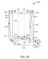
図3Aは、いくつかの実施形態に係る、例示的なカメラアセンブリ300Aを示す。カメラアセンブリ300Aは、光源310、光ガイド324、ハウジング308、レンズ312、フィルタ318、及び、カメラ314を備える場合がある。FIG. 3A illustrates an
光源310は、光ガイド324と結合され、IR光320を発するように構成される場合がある。光源310は、LED、VCSEL、レーザーダイオード、又は、可視スペクトル及び/又はNIR若しくはSWIRを含む(しかしこれらに限定されない)IRスペクトルの光の波長を放出可能な他の光源を含む場合がある。The
光ガイド324は、光源310によって発されたIR光320を、カメラアセンブリ300Aから外向き方向(又は第2方向)に指向するように構成される場合がある。いくつかの実施形態では、光ガイド324は、透明なポリカーボネートなどの透明な材料を含む場合がある。さらに、光ガイド324は、光を反射するように構成される場合がある。例えば、いくつかの実施形態では、光ガイド324は、光ガイド324の内面(ハウジング308の外面を含み得る)がハウジング308の内面の屈折率よりも大きい屈折率を有するところ、光を反射するように構成される場合がある。他の例として、光ガイド324は、光ガイド324の内面(ハウジング308の外面を含み得る)が反射面を含み、ハウジング308の内面が黒ずんだ表面、又は、可視光若しくはIR(例えば、NIR及び/又はSWIR)光を吸収可能な表面を含むところ、光を反射するように構成される場合がある。いくつかの実施形態では、光ガイド324は、光ファイバーを含む場合があり、他の実施形態では、光ガイド324は、ミラー及び/又は反射器を含む場合がある。更に、光ガイド324は、(例えば、成形体を介して)ハウジング308と結合される場合がある。The
レンズ312は、内向き方向(または第1方向)で、可視光322をカメラアセンブリ300Aの外側からカメラ314に伝達するように構成された光学レンズ又はレンズの組立体である。いくつかの態様では、レンズ312は、可視光322をカメラ314に合焦するように構成される場合がある。いくつかの実施形態では、レンズ312は、アクリルを含む場合がある。
カメラ314は、能動型のピクセルセンサ又は光センサのアレイ(例えば、フォトダイオード、CMOSイメージセンサアレイ、CCDアレイ、及び/又は、可視スペクトル、IRスペクトル(例えば、NIR又はSWIR)、若しくは、紫外線スペクトルの波長の光を検出可能な他の任意のセンサ)を備える場合がある。いくつかの実施形態では、カメラ314はRGBカメラを含む場合がある。更に、カメラ314は、光源310がIR光320を発している間に可視光322を検出するように構成される場合がある。更に、カメラ314は、物体又は光景が近景又は遠景のいずれでもイメージングされる広範囲イメージングを実行するように構成される場合がある。The
フィルタ318は、カメラ314とレンズ312との間に配置される。フィルタ318は、IRカットフィルタを含む場合がある。フィルタ318は、IR光がカメラ314に干渉しないように、光のIR波長(例えば、中赤外波長、NIR、又は、SWIRの光)を反射及び/又は遮断するように構成される場合がある。Filter 318 is disposed between
ハウジング308は、レンズ312を囲み、フィルタ318及びカメラ314を取り囲む場合がある。上述のとおり、ハウジング308の内面(例えば、カメラ314に面する壁)は、黒ずんだ表面、又は、可視光若しくはIR(例えば、NIR及び/又はSWIR)光を吸収可能な表面を含む場合がある。図3Aに示すように、第1表面358は、ハウジング308の上部、レンズ312の上部、及び、光ガイド324の側面によって形成される。更に、長さL1は、第1表面358におけるハウジング308の上部から、カメラ314の近くのハウジング308の基部までを計測した、ハウジング308の長さである。いくつかの実施形態では、ハウジング308の長さL1を最小化することが有利であり得る。 The
作動中に、光源310は、光ガイド324及び第1表面358を通って指向されるIR(例えば、NIRまたはSWIR)光320を発する場合がある。IR光320は、カメラアセンブリ300A及びカメラ314の前の光景を照らす場合がある。光景内の物体は、IR光320の少なくとも一部を、カメラアセンブリ300Aと、カメラアセンブリ300Aに近接して配置されたディスプレイと、に戻る方向に反射する場合がある。反射されたIR光320の一部は、表示ピクセル及び/又は表示サブピクセルの間の孔を通過し、ディスプレイの背後に配置されたIRカメラによって検出され得る。各IRカメラは、検出されたIR光を画像に撮影する場合がある。当該撮影された画像は、深度感知に適している場合がある。During operation, the
図3Aを参照して、いくつかの実施形態では、光源310は、IR(例えば、NIR又はSWIR)光320を発するように構成される場合があり、カメラ314は、IR光320及び/又は可視光322を検出するように構成される場合がある。更に、いくつかの実施形態では、光源310は、カメラ314がIR光320及び/又は可視光322を検出する間に、IR光320を発するように構成される場合がある。例えば、イメージング中に、光源310は、光ガイド324及び第1表面358を通ってカメラアセンブリ300Aの前面にガイドされる、IR光320を発する場合がある。IR光320の一部は、カメラアセンブリ300Aの前の物体又は造作物で反射し、レンズ312を透過してカメラ314に到達する場合がある。このように、カメラアセンブリ300Aは、イメージングのためにIR光を放出可能、かつ、感知可能である場合がある。3A, in some embodiments, the
他の実施形態では、光源310は、可視光を発するように構成される場合がある。イメージング中に、光源310は、光ガイド324および第1表面358を通ってカメラアセンブリ300Aの前面にガイドされる可視光を発する場合がある。可視光の一部は、カメラアセンブリ300Aの前の物体または造作物で反射し、そして、レンズ312を通過してカメラ314に到達する場合がある。このように、カメラアセンブリ300Aは、イメージングのために可視光を放出可能、かつ、感知可能である場合がある。In other embodiments, the
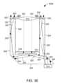
図3Bは、いくつかの実施形態に係る、例示的なカメラアセンブリ300Bを示す。カメラアセンブリ300Bは、図3Aを参照して上記で説明されたカメラアセンブリ300Aの一実施形態であり得る。図3Bに示すように、カメラアセンブリ300Bは2個の光源310を備えるが、いくつかの実施形態では、カメラアセンブリ300Bは2個より多い光源を備える場合がある。各光源310は、光ガイド324に結合される場合がある。更に、各光源310は、LED、VCSEL、レーザーダイオード、又は、NIR若しくはSWIRを含むがこれに限定されないIRスペクトルの光の波長を放出可能な他の光源を含む場合がある。作動中、各光源310は、光ガイド324を通ってカメラアセンブリ300Bの前面に向かって伝搬するIR光320を発する場合がある。図2及び図3Aを参照して上記で説明されたように、IR(例えば、NIR又はSWIR)光320は、カメラアセンブリ300Bの前の物体又は造作物で反射し、深度感知及び画像処理のために、アンダーディスプレイIRカメラによって検出される場合がある。FIG. 3B illustrates an
図3Cは、いくつかの実施形態に係る、例示的なカメラアセンブリ300Cを示す。カメラアセンブリ300Cは、図3A及び/又は図3Bを参照して上記で説明されたカメラアセンブリ300A及び/又はカメラアセンブリ300Bの一実施形態であり得る。図3Cに示すように、カメラアセンブリ300Cは可視スペクトルまたはIR(例えば、NIR又はSWIR)スペクトルの光の波長を検出可能なカメラ314を備える。更に、カメラアセンブリ300Cは、可視スペクトルまたはIR(例えば、NIR又はSWIR)スペクトルの光の波長を放出可能な光源310を備える。3C illustrates an
図3Cに示すように、カメラアセンブリ300Cはまた、光ガイド324を備える。光ガイド324は、拡散面326を備える。拡散面326は、光源310によって発された光320(例えば、可視光、NIR光、又は、SWIR光)を拡散し、広げ、又は、散乱するように構成される場合がある。拡散面326は、ハウジング308の周りにリングを形成する第1表面358の一部を含む場合がある。更に、拡散面326は、光ガイド324の一部を含む場合がある。例えば、拡散面326は、成形を介して光ガイド324と統合される場合がある。いくつかの実施形態では、拡散面326は、ある粗さを有する回折格子を含む場合がある。より詳細には、回折格子は、多数の微細な溝、スリット、又は、隆起を含み得る。いくつかの実施形態では、溝、スリット、及び/又は、隆起は、ランダムに配置される場合がある。あるいは、それらは、パターンを形成するために、平行又は均一な態様で配置される場合がある。このように、拡散面326は、光320の、均一な照明プロファイル、又は、調整された照明パターンを提供するように構成される場合がある。As shown in FIG. 3C, the
図3Dは、いくつかの実施形態に係る、例示的なカメラアセンブリ300Dを示す。カメラアセンブリ300Dは、図3A、図3B、及び/又は、図3Cを参照して上記で説明されたカメラアセンブリ300A、カメラアセンブリ300B、及び/又は、カメラアセンブリ300Cの一実施形態であり得る。図3Dに示すように、光ガイド324は、レンズ及び/又はマイクロレンズ328(「マイクロレンズ328」)を含む。いくつかの実施形態では、複数のマイクロレンズ328は、ハウジング308の周りにリングを形成する第1表面358の一部に統合(例えば、成形)される場合がある。マイクロレンズ328は、光源310によって発されるIR光320を拡散及び/又は回折するように構成される場合がある。3D illustrates an
図3Eは、いくつかの実施形態に係る、例示的なカメラアセンブリ300Eを示す。カメラアセンブリ300Eは、図3A-図3Dを参照して上記で説明されたカメラアセンブリ300A、カメラアセンブリ300B、カメラアセンブリ300C、及び/又は、カメラアセンブリ300Dの一実施形態であり得る。図3Eに示すように、光ガイド324は、ハウジング308の両側に配置された、2個のマイクロレンズ330を含む。いくつかの実施形態では、2個よりも多いマイクロレンズ330が、ハウジング308の各側面に、ハウジング308の周りにリングを形成する光ガイド324の表面に沿って配置され得る。マイクロレンズ330は、光源310によって発された光を拡散及び/又は回折するように構成される場合がある。3E illustrates an
図3Fは、いくつかの実施形態に係る、例示的なカメラアセンブリ300Fを示す。カメラアセンブリ300Fは、図3A-図3Eを参照して上記で説明されたカメラアセンブリ300A、カメラアセンブリ300B、カメラアセンブリ300C、カメラアセンブリ300D、及び/又は、カメラアセンブリ300Eの一実施形態であり得る。いくつかの実施形態では、カメラアセンブリ300Fは、環境光センサ352を備える場合がある。環境光センサ352は、カメラアセンブリ300Fの前の環境光の量を検出するように構成される場合がある。感知中、カメラアセンブリ300Fの前の環境光350は、光ガイド324を通って環境光センサ352にガイドされ得る。そのため、カメラアセンブリ300Fは、例えば、カメラアセンブリ300Fに結合されたディスプレイスクリーンの輝度を調節するために、環境光を測定可能である場合がある。3F illustrates an
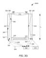
図3Gは、いくつかの実施形態に係る、例示的なカメラアセンブリ300Gを示す。カメラアセンブリ300Gは、図3A-図3Fを参照して上記で説明されたカメラアセンブリ300A、カメラアセンブリ300B、カメラアセンブリ300C、カメラアセンブリ300D、カメラアセンブリ300E、及び/又は、カメラアセンブリ300Fの一実施形態であり得る。FIG. 3G illustrates an
図3Gに示すように、カメラアセンブリ300Gは、光を反射するように構成される場合がある光ガイド324を備える。いくつかの実施形態では、光ガイド324は、光ガイド324の内面が、ハウジング308の内面の屈折率よりも大きい屈折率を有するところ、光を反射するように構成され得る。更に、いくつかの実施形態では、光ガイド324の内面が反射面を含む一方、ハウジング308の内面が、黒ずんだ表面、又は、可視光若しくはIR光(例えば、NIR光及び/又はSWIR光)を吸収可能な表面を含むところ、光を反射するように構成される場合がある。As shown in FIG. 3G, the
いくつかの実施形態では、カメラアセンブリ300Gは、近接センサ354を備える場合がある。近接センサ354は、光源310によって発されたIR(例えば、NIR又はSWIR)光320を検出するように構成される場合がある。感知中、光源310は、光ガイド324を通ってカメラアセンブリ300Gの前面にガイドされ得るIR光320を発する場合がある(簡単にするために、発されたIR光320は図示されていない)。IR光320の一部は、カメラアセンブリ300Gの前の物体又は造作物で反射し、光ガイド324を通って近接センサ354に戻るように伝搬する場合がある。そのため、カメラアセンブリ300Gは、例えばユーザの存在を検出するために、IR光を放出可能、及び、感知可能である場合がある。In some embodiments, the
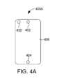
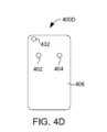
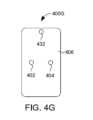
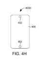
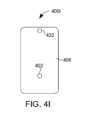
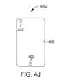
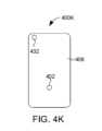
図4A-4Kは、いくつかの実施形態に係る、例示的な電子システム400A-400Kを示す。電子システム400A-400Kはそれぞれ、カメラアセンブリ432と、カメラ402及び/又はカメラ404と、ディスプレイ406と、を備える。カメラアセンブリ432は、図2及び図3A-3Gのカメラアセンブリ200、及び/又は、カメラアセンブリ300A-300Gの一実施形態であり得る。カメラ402及びカメラ404はそれぞれ、図1のカメラ102及び/又はカメラ104の一実施形態であり得る。更に、カメラ402及び404はそれぞれ、ディスプレイ406の下に配置され、深度感知のために画像を撮影するように構成される場合がある。Figures 4A-4K show exemplary
図4Aに示すように、カメラアセンブリ432は、電子システム400Aの角の近くに配置される。また、カメラ402及びカメラ404は、長軸に沿って、電子システム400Aの端部の近辺に配置される。As shown in FIG. 4A,
作動中、IR(例えば、NIR又はSWIR)光は、カメラアセンブリ432の光源によって放出され、カメラアセンブリ432の前方の光景を照らす場合がある。光景内の物体は、IR光の少なくとも一部を、カメラアセンブリ432およびディスプレイ406に向かって戻る方向に反射する場合がある。反射されたIR光の一部は、ディスプレイ406のピクセル及び/又はサブピクセル間の孔を通過し、ディスプレイ406の背後に配置されたIRカメラ402及びIRカメラ404によって検出され得る。カメラ402及びカメラ404のそれぞれは、検出されたIR光を画像に撮影する場合があり、撮影された画像は、深度感知に適している場合がある。In operation, IR (e.g., NIR or SWIR) light may be emitted by a light source in the
図4Bでは、カメラアセンブリ432は、電子システム400Bの角の近くに配置される。また、カメラ402及びカメラ404は、長軸に沿って、電子システム400Bの中央領域近辺に配置される。図1を参照して上記で論じたように、2台のカメラ間の距離は、深度感知の解像度に影響を与える。言い換えると、カメラ間の距離が大きいほど、カメラによって撮影された画像から取得可能な深度情報の量が多くなる。図4Aと比べて、図4Bのカメラ402及びカメラ404は、より短い距離で隔たれている。その結果、図4Aのカメラ402及びカメラ404は、図4Bのカメラ402及びカメラ404よりも高い解像度の深度感知をサポートし得る。In FIG. 4B, the
図4Cは、電子システム400Cの角の近くに配置されたカメラアセンブリ432と、短軸に沿って電子システム400Cの中央領域近辺に配置されたカメラ402及びカメラ404と、を示す。図4Dは、短軸に沿って、電子システム400Dの角の近くに配置されたカメラアセンブリ432と、電子システム400Dの上部に配置されたカメラ402及びカメラ404と、を示す。Figure 4C shows a
図4Eは、電子システム400Eの一端の近辺に配置されたカメラアセンブリ432を示す。カメラ402及びカメラ404は、カメラアセンブリ432と一列に並んで長軸に沿って配置される。図4Fでは、カメラアセンブリ432は、電子システム400Fの一端の近辺に配置される。カメラ402及びカメラ404は、カメラアセンブリ432と一列に並んで長軸に沿って配置される。図4Eと異なり、図4Fのカメラ402及びカメラ404は、より短い距離で隔たれている。その結果、図4Eのカメラ402及びカメラ404は、図4Fのカメラ402及びカメラ404よりも高い解像度の深度感知をサポートし得る。FIG. 4E shows a
図4Gは、電子システム400Gの一端の近辺に配置されたカメラアセンブリ432を示す。カメラ402及びカメラ404は、短軸に沿って電子システム400Gの中央領域近辺に配置される。FIG. 4G shows
図4Hは、電子システム400Hの一端の近辺に配置されたカメラアセンブリ432と、電子システム400Hの他端の近辺に配置されたカメラ402と、を示す。いくつかの実施形態では、カメラアセンブリ432及びカメラ402の両方が、深度感知のための画像を撮影するように構成される場合がある。FIG. 4H shows a
図4Iは、電子システム400Iの一端の近辺に配置されたカメラアセンブリ432と、電子システム400Iの中央領域の近辺に配置されたカメラ402と、を示す。いくつかの実施形態では、カメラアセンブリ432及びカメラ402の両方が、深度感知のための画像を撮影するように構成される場合がある。FIG. 4I shows a
図4Jは、電子システム400Jの一つの角の近辺に配置されたカメラアセンブリ432と、電子システム400Jの端部の近辺に配置されたカメラ402と、を示す。いくつかの実施形態では、カメラアセンブリ432及びカメラ402の両方が、深度感知のための画像を撮影するように構成される場合がある。FIG. 4J shows a
図4Kは、電子システム400Kの一つの角の近辺に配置されたカメラアセンブリ432と、電子システム400Kの中央領域近辺に配置されたカメラ402と、を示す。いくつかの実施形態では、カメラアセンブリ432及びカメラ402の両方が、深度感知のための画像を撮影するように構成される場合がある。FIG. 4K shows a
図5は、いくつかの実施形態に係る、例示的な電子システム500の断面を示す。電子システム500は、図1及び図4A-4Gの電子システム100及び/又は電子システム400A-400Gの一実施形態であり得る。図5に示すように、電子システム500は、カメラアセンブリ532、ディスプレイ層506、及び、モジュール540を備える。カメラアセンブリ532は、図2及び図4A-4Gのカメラアセンブリ200及び/又はカメラアセンブリ432の一実施形態であり得る。モジュール540は、カメラ502及びカメラ504を備える。カメラ502及びカメラ504はそれぞれ、図1及び図4A-4Gのカメラ102、カメラ104、カメラ402、及び/又は、カメラ404の一実施形態であり得る。5 illustrates a cross-section of an exemplary
カメラアセンブリ532は、光源510、反射器516、レンズ512、カメラ514、フィルタ518、及び、ハウジング508を備える。更に、長さL1は、第1表面558におけるハウジング508の上部から、カメラ514の近くのハウジング508の基部までを計測した、ハウジング508の長さである。いくつかの実施形態では、ハウジング508の長さL1を最小化することが有利であり得る。長さL1は、(ディスプレイ層506およびモジュール540の長さにわたる)長さL2よりも短く見えるが、L1は長さL2と比べて短い、等しい、又は、長い、といったほぼ任意の長さであり得る。加えて、カメラアセンブリ532は、ディスプレイ層506及びモジュール540に隣接して示されているが、実際の実装では、コンポーネント(図示せず)が、カメラアセンブリ532をディスプレイ層506及びモジュール540から分離する場合がある。 The
ディスプレイ層506は、OLEDディスプレイまたはマイクロLEDディスプレイといった多孔性ディスプレイの複数の層を含む場合がある。図5に示すように、ディスプレイ層506は、ディスプレイ表面536及び発光層538を含む場合がある。いくつかの実施形態では、発光層538は、複数の表示ピクセル及び/又は表示サブピクセルを含み、各表示ピクセル及び/又は表示サブピクセルの間に穴、ギャップ、又は、空のスペースを有する場合がある。The
モジュール540は、ディスプレイ層506の下に配置され、カメラ502及びカメラ504と、対応するレンズ542と、を備える場合がある。カメラ502及びカメラ504は、物体または光景が近景又は遠景のいずれでもイメージングされる広範囲イメージングを実行するように構成されたIRのCMOSセンサを備える場合がある。カメラ502及びカメラ504は、指、手、及び、頭といった物体を迅速に感知するように更に構成される場合がある。更に、カメラ502及びカメラ504はそれぞれ、深度感知のために画像を撮影するように構成される場合がある。深度感知の解像度は、カメラ502とカメラ504の間の距離である分離Dに依存し得る。言い換えれば、距離Dが大きいほど、カメラ502及びカメラ504によって撮影された画像から導出可能な深度情報の量は大きくなる。The
作動中に、光源510は、IR(例えば、NIRまたはSWIR)光520を発する場合がある。IR光520は、反射器516で反射し、レンズ512を透過する。IR光520は、カメラアセンブリ532と、カメラ502及びカメラ504と、の前の光景を照らす場合がある。光景内の物体は、IR光520の少なくとも一部を、ディスプレイ層506に戻る方向に、例えば、反射光520(R)(1)及び反射光520(R)(2)として反射する場合がある。反射光520(R)(1)及び反射光520(R)(2)の一部は、発光層538内の表示ピクセル及び/又は表示サブピクセルによって遮られる一方、反射光520(R)(1)及び反射光520(R)(2)の残りは、表示ピクセル及び/又は表示サブピクセルの間の孔を通過する場合がある。孔とレンズ542を通過した反射光520(R)(1)及び反射光520(R)(2)は、カメラ502及びカメラ504によってそれぞれ検出され得る。カメラ502及びカメラ504のそれぞれは、これら反射されたIR光をそれぞれに別々の画像として撮影する場合がある。これらの撮影された画像は、深度感知のために組み合わせられる場合がある。In operation, the
図6は、いくつかの実施形態に係る、例示的な電子システム600の断面を示す。電子システム600は、図4H-4Kの電子システム400H-400Kのうちのいずれかの一実施形態であり得る。図6に示すように、電子システム600は、カメラアセンブリ632、ディスプレイ層606、及び、モジュール640を備える。カメラアセンブリ632は、図2、図4A-4K、及び、図5のカメラアセンブリ200、カメラアセンブリ432、及び/又は、カメラアセンブリ532の一実施形態であり得る。ディスプレイ層606は、図5のディスプレイ層506の一実施形態であり得る。図6に示すように、モジュール640は、カメラ604を備える。カメラ604は、図1、図4A-4K、及び、図5のカメラ102、カメラ104、カメラ402、カメラ404、カメラ502、及び/又は、カメラ504の一実施形態であり得る。6 illustrates a cross-section of an exemplary
作動中に、光源610は、IR(例えば、NIRまたはSWIR)光620を発する場合がある。IR光620は、反射器616で反射し、レンズ612を透過する。IR光620は、カメラアセンブリ632とカメラ604の前の光景を照らす場合がある。光景内の物体は、IR光620の少なくとも一部を、ディスプレイ層606に戻る方向に、例えば、反射光620(R)として反射する場合がある。反射光620(R)の一部は、ディスプレイ層606とレンズ642とを透過し、カメラ604によって検出され、画像として撮影される場合がある。いくつかの実施形態では、光源610がIR光620を放出するのと実質的に同時に、カメラ614は、光景内の物体で反射する(例えば、太陽又は他の光源からの)可視光622を検出し、当該可視光622を画像に撮影する場合がある。カメラ614及びカメラ604よって撮影された画像は、深度感知のために組み合わせられる場合がある。During operation, the
図7は、いくつかの実施形態に係る、例示的な電子システム700の断面を示す。電子システム700は、図1及び図4A-4Gの電子システム100、及び/又は、電子システム400A-400Gの一実施形態であり得る。図7に示すように、電子システム700は、カメラアセンブリ732、ディスプレイ層706、及び、モジュール740を備える。カメラアセンブリ732は、図3A-3Gにおける、カメラアセンブリ300A、及び/又は、カメラアセンブリ300B-300Gのいずれかの一実施形態であり得る。ディスプレイ層706は、図5及び図6のディスプレイ層506及び/又はディスプレイ層606の一実施形態であり得る。更に、モジュール740は、図5のモジュール540の一実施形態であり得る。7 illustrates a cross-section of an exemplary
カメラアセンブリ732は、光源710、光ガイド724、レンズ712、カメラ714、フィルタ718、及び、ハウジング708を備える。いくつかの実施形態では、カメラアセンブリ732は、図3B-3Gに示すように、追加的な光源、散乱面、マイクロレンズ、環境光センサ、及び/又は、近接センサを更に備える場合がある。The
長さL1は、第1表面758におけるハウジング708の上部から、カメラ714の近くのハウジング708の基部までを計測した、ハウジング708の長さである。いくつかの実施形態では、ハウジング708の長さL1を最小化することが有利であり得る。更に、長さL1は、(ディスプレイ層706およびモジュール740の長さにわたる)長さL2よりも短く見えるが、L1は長さL2と比べて短い、等しい、又は、長い、といったほぼ任意の長さであり得る。加えて、カメラアセンブリ732は、ディスプレイ層706及びモジュール740に隣接して示されているが、実際の実装では、コンポーネント(図示せず)が、カメラアセンブリ732をディスプレイ層706及びモジュール740から分離する場合がある。 LengthL1 is the length of
作動中に、光源710は、IR(例えば、NIRまたはSWIR)光720を発する場合がある。IR光720は、光ガイド724と第1表面758を通って指向される場合がある。IR光720は、カメラ702、カメラ704、及び、カメラ714の前の光景を照らす場合がある。光景内の物体は、IR光720の少なくとも一部を、ディスプレイ層706に戻る方向に、例えば、反射されたIR光720(R)(1)及びIR光720(R)(2)として反射する場合がある。反射されたIR光720(R)(1)及びIR光720(R)(2)の一部は、ディスプレイ層706とレンズ742とを透過し、カメラ702及びカメラ704によってそれぞれに検出される場合がある。カメラ702及びカメラ704は、これらのIR光をそれぞれに別々の画像として撮影する場合があり、これらの画像は、深度感知のために組み合わせられる場合がある。In operation, the
図8は、いくつかの実施形態に係る、例示的な電子システム800の断面を示す。電子システム800は、図4H-4Kの電子システム400H-400Kのうちの任意のものの一実施形態であり得る。図8に示すように、電子システム800は、カメラアセンブリ832、ディスプレイ層806、及び、モジュール840を備える。カメラアセンブリ832は、図3A-3Gの、カメラアセンブリ300A、及び/又は、カメラアセンブリ300B-カメラアセンブリ300Gの一実施形態であり得る。ディスプレイ層806は、図5-7のディスプレイ層506、ディスプレイ層606、及び/又は、ディスプレイ層706の一実施形態であり得る。更に、モジュール840は、カメラ804を備える。カメラ804は、図1、図4A-4K、及び、図5-7のカメラ102、カメラ104、カメラ402、カメラ404、カメラ502、カメラ504、カメラ604、カメラ702、及び/又は、カメラ704の一実施形態であり得る。いくつかの実施形態では、カメラ804は、IR(例えば、NIR又はSWIR)光を検出するように構成される場合があり、フィルタ818はカメラ804を可視光からシールドする場合がある。FIG. 8 illustrates a cross-section of an exemplary
作動中に、光源810は、光ガイド824及び第1表面858を通って指向されるIR(例えば、NIRまたはSWIR)光820を発する場合がある。IR光820は、カメラ804及びカメラ814の前の光景を照らす場合がある。光景内の物体は、IR光820の少なくとも一部を、カメラアセンブリ800及びディスプレイ層806に戻る方向に、例えば、反射されたIR光820(R)(1)及びIR光820(R)(2)として反射する場合がある。反射光820(R)(1)の一部は、ディスプレイ層806とレンズ842とを透過し、カメラ804によって検出され、画像として撮影される場合がある。更に、反射光820(R)(2)の一部は、カメラ814へ向かってレンズ812及びフィルタ818を透過する場合があり、当該カメラ814は、反射光820(R)(2)を画像として撮影する場合がある。カメラ804及びカメラ814によって撮影された画像は、深度感知のために組み合わせられる場合がある。In operation, the
いくつかの実施形態では、カメラ814は可視光を検出するように構成される場合があり、フィルタ818はカメラ814をIR光からシールドする場合がある。作動中に、光源810は、光ガイド824及び第1表面858を通って指向されるIR(例えば、NIRまたはSWIR)光820を発する場合がある。IR光820は、カメラ804及びカメラ814の前の光景を照らす場合がある。光景内の物体は、IR光820(R)(1)の少なくとも一部を、例えば、反射光820(R)(1)として、ディスプレイ層806に戻る方向に反射する場合がある。反射光820(R)(1)の一部は、ディスプレイ層806とレンズ842とを透過し、カメラ804によって検出され、画像として撮影される場合がある。いくつかの実施形態では、光源810がIR光820を放出するのと実質的に同時に、カメラ814は、光景内の物体で反射する(例えば、太陽又は他の光源からの)可視光822を検出し、当該可視光822を画像に撮影する場合がある。カメラ814及びカメラ804よって撮影された各画像は、深度感知のために組み合わせられる場合がある。In some embodiments, the
図9は、いくつかの実施形態に係る、ディスプレイの下に配置されたカメラによって撮影された例示的な画像900を示す。画像900は、例えば、図1、図4A-4K、図5-8のカメラ102、カメラ104、カメラ402、カメラ404、カメラ502、カメラ504、カメラ604、カメラ702、カメラ704、又は、カメラ804といった、多孔性ディスプレイの背後または下に配置されたカメラによって撮影され得る。図9に示すように、画像900は、暗線及び明点のグリッド、又は、「スクリーンドア効果」を含む。暗線は、表示ピクセル及び/又は表示サブピクセルのパターンに対応する。暗線は、表示ピクセル及び/又は表示サブピクセルが、光の一部がディスプレイを通過することを妨げることにより生成される。一方、明点は、表示ピクセル及び/又は表示サブピクセル間のギャップ又は孔に対応する。明点は、下にあるカメラに向かってディスプレイの孔又はギャップを通過する光によって生成される。9 illustrates an
いくつかの実施形態では、アンダーディスプレイカメラによって撮影された画像は、スクリーンドアの複数の層(又はスクリーンドアの積層体)を通してアンダーディスプレイカメラが同時にイメージングしているかのように現れるグリッド、又は、スクリーンドア効果を含む場合がある。ここで、スクリーンドアの各層は異なるピッチ(例えば、孔のサイズ又は密度)を有する。このような実施形態では、光は、スクリーンドア層の表示ピクセル及び/又は表示サブピクセルの間の孔又はギャップを通過する場合がある。更に、光の各点は水平方向及び垂直方向の異なる位置に拡散される(例えば、点像分布関数として)。また、IR光の各点は画像にわたって同様の方法で拡散され、これは大きな歪みをもたらす場合がある。In some embodiments, the image captured by the under-display camera may include a grid, or screen door effect, that appears as if the under-display camera is imaging through multiple layers of screen door (or stacks of screen doors) simultaneously, where each layer of screen door has a different pitch (e.g., hole size or density). In such embodiments, light may pass through holes or gaps between display pixels and/or display sub-pixels in the screen door layers. Furthermore, each point of light is spread to different positions horizontally and vertically (e.g., as a point spread function). Also, each point of IR light is spread in a similar manner across the image, which may result in significant distortion.
図9に示すように、画像900の一部は、ディスプレイの表示ピクセル及び/又は表示サブピクセルによって不明瞭になっている。言い換えれば、表示ピクセル及び/又は表示サブピクセルは、感知に利用可能な光の量を低減し、アンダーディスプレイカメラのFOVを事実上遮る場合がある。そのため、いくつかの実施形態では、スクリーンドア効果、歪み、又は他のアーティファクトを除去するために、撮影された画像をフィルタリング又は較正される場合がある。As shown in FIG. 9, portions of the
図10は、いくつかの実施形態に係る、画像処理システム1000のブロック図である。画像処理システム1000は、デバイスインタフェース1010、プロセッサ1020、及び、メモリ1030を備える。本明細書での議論の目的で、図10のプロセッサ1020は、デバイスインタフェース1010及びメモリ1030と結合されるものとして示されている。実際の実施形態では、デバイスインタフェース1010、プロセッサ1020、及び/又は、メモリ1030は、1以上のバス(簡略化のために図示せず)を用いて一緒に接続される場合がある。いくつかの実施形態では、画像処理システム1000は、図1、図4A-4K、及び、図5-8を参照して説明された電子システム100、電子システム400A-400K、及び/又は、電子システム500-800の、特定用途向け集積回路(application specific integrated circuit)(ASIC)、又は、他の集積回路(integrated circuit)(IC)であってもよい。10 is a block diagram of an image processing system 1000 according to some embodiments. The image processing system 1000 comprises a device interface 1010, a processor 1020, and a memory 1030. For purposes of discussion herein, the processor 1020 of FIG. 10 is shown as being coupled to the device interface 1010 and the memory 1030. In an actual embodiment, the device interface 1010, the processor 1020, and/or the memory 1030 may be coupled together using one or more buses (not shown for simplicity). In some embodiments, the image processing system 1000 may be an application specific integrated circuit (ASIC) or other integrated circuit (IC) of the
デバイスインタフェース1010は、1以上のカメラ、カメラアセンブリ、及び/又は、ディスプレイを含む(しかしこれらに限定されない)入力デバイスに信号を送信し、入力デバイスから信号を受信する場合がある。いくつかの実施形態では、デバイスインタフェース1010は、ディスプレイインタフェース1012を備える場合がある。ディスプレイインタフェース1012は、ディスプレイと通信するために、及び/又は、画像処理システム1000のユーザに視覚的なインタフェースを提供するために使用される場合がある。いくつかの実施形態では、デバイスインタフェース1010は、RGBカメラインタフェース1014と、IRカメラインタフェース1016及びIRカメラインタフェース1018と、を更に備える場合がある。RGBカメラインタフェース1014と、IRカメラインタフェース1016及びIRカメラインタフェース1018と、はそれぞれに異なるカメラと通信するために用いられる場合がある。例えば、RGBカメラインタフェース1014は、物体又は光景の画像を撮影するために、起動信号をカメラ514又はカメラ714に送信し、これらのカメラからセンサ情報を受信する場合がある。更に、IRカメラインタフェース1016及びIRカメラインタフェース1018は、物体及び/又は光景のIR画像を撮影するために、例えば、カメラ502、カメラ504、カメラ702、又は、カメラ704に起動信号を送信し、これらのカメラからセンサ情報を受信する場合がある。The device interface 1010 may send signals to and receive signals from input devices, including, but not limited to, one or more cameras, camera assemblies, and/or displays. In some embodiments, the device interface 1010 may include a display interface 1012. The display interface 1012 may be used to communicate with a display and/or provide a visual interface to a user of the image processing system 1000. In some embodiments, the device interface 1010 may further include an RGB camera interface 1014, an IR camera interface 1016, and an IR camera interface 1018. The RGB camera interface 1014, the IR camera interface 1016, and the IR camera interface 1018 may each be used to communicate with a different camera. For example, the RGB camera interface 1014 may send an activation signal to the
メモリ1030は、カメラインタフェース1014、カメラインタフェース1016、及び/又はカメラインタフェース1018を介して受信した画像を記憶するための画像バッファ1032を備える場合がある。メモリ1030はまた、少なくとも次のSWモジュールを記憶し得る、非一時的なコンピュータ読取り可能な媒体(例えば、EPROM、EEPROM、フラッシュメモリ、ハードドライブ等といった、1以上の不揮発性メモリ素子)を備える場合がある。
●IRカメラインタフェース1016及び/又はIRカメラインタフェース1018(又は、アンダーディスプレイカメラと通信する他のインタフェース)を介して受信した画像をフィルタリングする画像フィルタリングSWモジュール1034であり、画像フィルタリングSWモジュール1034は更に以下を備える:
〇IRカメラインタフェース1016及び/又はIRカメラインタフェース1018を介して受信した画像からノイズをフィルタリング、低減、又は、除去するニューラルネットワークモデル1035と、
●(i)IRカメラインタフェース1016及びIRカメラインタフェース1018の両方、又は、(ii)RGBカメラインタフェース1014と、IRカメラインタフェース1016又はIRカメラインタフェース1018のいずれか、を介して受信した画像を組み合わせ、例えば立体視を用いて画像から深度情報を抽出する、深度マップSWモジュール(又は、深度マップジェネレータ)1036。 Memory 1030 may include an image buffer 1032 for storing images received via camera interface 1014, camera interface 1016, and/or camera interface 1018. Memory 1030 may also include a non-transitory computer readable medium (e.g., one or more non-volatile memory elements such as EPROM, EEPROM, flash memory, a hard drive, etc.) that may store at least the following SW modules:
An image filtering SW module 1034 that filters images received via the IR camera interface 1016 and/or the IR camera interface 1018 (or other interface that communicates with the under-display camera), the image filtering SW module 1034 further comprising:
A neural network model 1035 that filters, reduces, or removes noise from images received via IR camera interface 1016 and/or IR camera interface 1018; and
●(i) a depth map SW module (or depth map generator) 1036 that combines images received via both IR camera interface 1016 and IR camera interface 1018, or (ii) the RGB camera interface 1014 and either the IR camera interface 1016 or the IR camera interface 1018, and extracts depth information from the images, for example using stereoscopic vision.
各ソフトウェアモジュールは、プロセッサ1020によって実行されると、対応する機能を画像処理システム1000に実行させる命令を含む。Each software module contains instructions that, when executed by the processor 1020, cause the image processing system 1000 to perform a corresponding function.
例えば、プロセッサ1020は、画像フィルタリングSWモジュール1034を実行して、IRカメラインタフェース1016及び/又はIRカメラインタフェース1018を介して受信した画像をフィルタリングする場合がある。画像フィルタリングSWモジュール1034を実行する際に、プロセッサ1020は、ニューラルネットワークモデル1035を用いて、IRカメラインタフェース1016及び/又はIRカメラインタフェース1018を介して受信した画像から(スクリーンドア効果のような)ノイズをフィルタリング、低減、又は、除去する場合がある。プロセッサ1020は、更に、深度マップSWモジュール1036を実行して、フィルタリングされた画像内の物体又は造作物の深度情報を決定する場合がある。例えば、深度マップジェネレータは、立体視を用いてフィルタリングされた画像を組み合わせて、当該組み合わされ、フィルタリングされた画像から深度情報を抽出する場合がある。深度マップジェネレータは、抽出された深度情報に少なくとも部分的に基づいて、物体又は造作物の深度マップを更に生成する場合がある。更に、プロセッサ1020は、深度情報に少なくとも部分的に基づいて、画像内の対象、物体、又は、造作物を認証する場合がある。For example, the processor 1020 may execute the image filtering SW module 1034 to filter the images received via the IR camera interface 1016 and/or the IR camera interface 1018. In executing the image filtering SW module 1034, the processor 1020 may use the neural network model 1035 to filter, reduce, or remove noise (such as a screen door effect) from the images received via the IR camera interface 1016 and/or the IR camera interface 1018. The processor 1020 may further execute the depth map SW module 1036 to determine depth information of objects or features in the filtered images. For example, the depth map generator may combine the filtered images using stereoscopic vision and extract depth information from the combined filtered images. The depth map generator may further generate a depth map of the object or feature based at least in part on the extracted depth information. Additionally, the processor 1020 may recognize objects, objects, or features within the image based at least in part on the depth information.
図9及び図10を参照して上記で説明したように、アンダーディスプレイカメラによって撮影された画像は、スクリーンドア効果、又は、他のノイズ、歪み、若しくは、干渉を含み得る。本開示の態様は、光(例えば、IR、NIR、又は、SWIRの反射光)がディスプレイを通過し、光の一部がディスプレイのピクセル及び/又はサブピクセルによって遮蔽され、一方で残りの光がピクセル及び/又はサブピクセル間の孔を通過してアンダーディスプレイカメラによって画像に撮影される、スクリーンドア効果が発生することを認識している。深度検知又は他の応用を容易にするために、画像フィルタは、ニューラルネットワークモデルを用いて画像からスクリーンドア効果をフィルタリングにより除去する場合がある。As discussed above with reference to FIGS. 9 and 10, images captured by an under-display camera may include a screen door effect or other noise, distortion, or interference. Aspects of the present disclosure recognize that a screen door effect occurs when light (e.g., IR, NIR, or SWIR reflected light) passes through a display and some of the light is blocked by pixels and/or subpixels of the display, while the remaining light passes through holes between the pixels and/or subpixels and is captured in an image by the under-display camera. To facilitate depth sensing or other applications, an image filter may use a neural network model to filter out the screen door effect from the image.
図11Aは、フィルタリング前の、アンダーディスプレイカメラによって撮影された例示的な画像1110を示している。図10を参照して、画像1110は、アンダーディスプレイIRカメラから、例えば、IRカメラインタフェース1016に送信される場合がある。IRカメラインタフェース1016は、記憶するために、例示的な画像1110を画像バッファ1032に送信する場合がある。図11Aに示すように、画像1110は、スクリーンドア効果によって不明瞭になっている。深度検知又は他の応用をサポートするために、画像フィルタリングSWモジュール1034は、例示的な画像1110をフィルタリングして、歪みを取り除く場合がある。FIG. 11A illustrates an example image 1110 captured by an under-display camera before filtering. Referring to FIG. 10, the image 1110 may be sent from the under-display IR camera to, for example, the IR camera interface 1016. The IR camera interface 1016 may send the example image 1110 to the image buffer 1032 for storage. As shown in FIG. 11A, the image 1110 is obscured by a screen door effect. To support depth sensing or other applications, the image filtering SW module 1034 may filter the example image 1110 to remove distortion.
図11Bは、フィルタリング後の、例示的な画像1120を示す。例示的な画像1120は、図11Aの例示的な画像1110のフィルタ後バージョンであり得る。図10を参照して、画像バッファ1032は、例示的な画像1110を画像フィルタリングSWモジュール1034に送信する場合がある。画像フィルタリングSWモジュール1034は、ニューラルネットワークモデル1035を用いて、例示的な画像1110からスクリーンドア効果をフィルタリングにより除去する場合がある。図11Bに示すように、フィルタリングされた画像1120は人物をより明確に表しており、深度検知又は他の応用に適している場合がある。FIG. 11B shows an example image 1120 after filtering. The example image 1120 may be a filtered version of the example image 1110 of FIG. 11A. Referring to FIG. 10, the image buffer 1032 may send the example image 1110 to the image filtering SW module 1034. The image filtering SW module 1034 may use a neural network model 1035 to filter out the screen door effect from the example image 1110. As shown in FIG. 11B, the filtered image 1120 more clearly depicts a person and may be suitable for depth sensing or other applications.
いくつかの実施形態では、ニューラルネットワークモデル1035は、撮影された画像からスクリーンドア効果又は他のノイズをフィルタリングにより除去するように学習されたCNNを含む場合がある。言い換えれば、CNNは、不明瞭な物体又は光景の画像から、元の物体若しくは光景の画像、又は、物体又は光景が明確な画像を推測するように学習される場合がある。いくつかの実施形態では、CNNは、元の物体又は光景の画像を少なくとも1つと、物体又は光景の不明瞭な画像を少なくとも1つと、を受信し、処理することによって学習され得る。いくつかの実施形態では、CNNの代わりに、又はCNNに加えて、点像分布逆関数変換を用いて画像をフィルタリングする場合がある。このように、画像フィルタリングSWモジュール1034は、ニューラルネットワークモデル1035及び/又は点像分布逆関数変換を用いて、アンダーディスプレイIRカメラからの画像をフィルタリングする場合がある。In some embodiments, the neural network model 1035 may include a CNN trained to filter out screen door effects or other noise from captured images. In other words, the CNN may be trained to infer an image of an original object or scene, or an image of a clear object or scene, from an image of an obscured object or scene. In some embodiments, the CNN may be trained by receiving and processing at least one image of the original object or scene and at least one image of the object or scene that is obscured. In some embodiments, instead of or in addition to a CNN, an inverse point spread function transform may be used to filter the images. Thus, the image filtering SW module 1034 may use the neural network model 1035 and/or an inverse point spread function transform to filter images from the under-display IR camera.
いくつかの撮影画像(例えば、不明瞭にされた、又は、フィルタリングされた画像)及び画像コンテンツ(例えば、深度情報、深度マップ、又は、識別された人物、物体、若しくは光景)は、図1、図4A-4K、及び、図5-8の電子システム100、電子システム400A-400K、及び/又は、電子システム500-800上の安全なリポジトリ(例えば、信頼された環境)に記憶される場合がある。安全なリポジトリは、信頼される環境内にあるアプリケーション及び/又はハードウェアのみが安全なリポジトリに記憶されたデータにアクセスし得るように、電子システムの他の部分から仮想的及び/又は物理的に分離されている場合がある。いくつかの態様では、安全なリポジトリは、少なくとも部分的に、メモリ1030内に形成される場合がある。よって、特定の撮影画像と画像コンテンツは、メモリ1030のうちの安全なリポジトリ内(例えば、画像バッファ1032内)に記憶される場合がある。Some captured images (e.g., obscured or filtered images) and image content (e.g., depth information, depth maps, or identified people, objects, or scenes) may be stored in a secure repository (e.g., a trusted environment) on the
いくつかの実施形態では、ニューラルネットワークモデル1035は、少なくとも部分的に、図1、図4A-4K、及び、図5-8の電子システム100、電子システム400A-400K、及び/又は、電子システム500-800内の、信頼される環境内に存在し得る。ニューラルネットワークモデル1035を信頼される環境内に置くことにより、ニューラルネットワークモデル1035は、保護された撮影画像及び画像コンテンツによって(例えば、CNNを用いた)機械学習が実行可能となる。In some embodiments, the neural network model 1035 may reside, at least in part, within a trusted environment within the
当業者は、様々な異なる任意のテクノロジー及び技術を用いて、情報及び信号が表し得ることを理解するであろう。例えば、上述の説明を通して参照され得るデータ、命令、コマンド、情報、信号、ビット、記号、及び、チップは、電圧、電流、電磁波、磁界又は磁性粒子、光場又は光粒子、あるいは、これらの任意の組合せによって表し得る。Those skilled in the art will appreciate that information and signals may be represented using any of a variety of different technologies and techniques. For example, the data, instructions, commands, information, signals, bits, symbols, and chips that may be referenced throughout the above description may be represented by voltages, currents, electromagnetic waves, magnetic fields or particles, optical fields or particles, or any combination thereof.
さらに、当業者は、本明細書で開示された態様に関連して説明された様々な例示的な論理ブロック、モジュール、回路、及び、アルゴリズムのステップが、電気的なハードウェア、コンピュータソフトウェア、又は、両者の組合せとして実装し得ることを理解しよう。このハードウェアとソフトウェアの交換可能性を明確に図示するために、例示的な様々なコンポーネント、ブロック、モジュール、回路、及び、ステップが、一般に、その機能の観点で上述のように説明されてきた。このような機能がハードウェア又はソフトウェアの何れで実装されるかは、システム全体に要求される特定のアプリケーションとデザイン上の制約に依存する。当業者は説明された機能を特定のアプリケーション毎に様々な方法で実装し得るが、そのような実装上の決定が、本開示の範囲からの逸脱を引き起こすと解釈されてはならない。Moreover, those skilled in the art will appreciate that the various example logic blocks, modules, circuits, and algorithmic steps described in connection with the aspects disclosed herein may be implemented as electrical hardware, computer software, or a combination of both. To clearly illustrate this interchangeability of hardware and software, the various example components, blocks, modules, circuits, and steps have been described above generally in terms of their functionality. Whether such functionality is implemented as hardware or software depends upon the particular application and design constraints required for the overall system. Those skilled in the art may implement the described functionality in varying ways for each particular application, but such implementation decisions should not be interpreted as causing a departure from the scope of the present disclosure.
本明細書で開示された態様に関連して説明された方法、手順、又はアルゴリズムは、ハードウェアにより直接的に、プロセッサによって実行されるソフトウェアモジュールにより、あるいは、両者の組合せにより、具体化され得る。ソフトウェアモジュールは、RAMメモリ、フラッシュメモリ、ROMメモリ、EPROMメモリ、EEPROMメモリ、レジスタ、ハードディスク、リムーバブルディスク、CD-ROM、又は、当技術分野において既知の他の形式の記憶媒体に常駐し得る。例示的な記憶媒体は、プロセッサが記憶媒体から情報を読み取り、記憶媒体に情報を書き込むことができるように、プロセッサに結合される。あるいは、記憶媒体はプロセッサに統合されてもよい。The methods, procedures, or algorithms described in connection with the aspects disclosed herein may be embodied directly in hardware, in software modules executed by a processor, or in a combination of both. The software modules may reside in RAM memory, flash memory, ROM memory, EPROM memory, EEPROM memory, registers, a hard disk, a removable disk, a CD-ROM, or any other form of storage medium known in the art. An exemplary storage medium is coupled to the processor such that the processor can read information from, and write information to, the storage medium. Alternatively, the storage medium may be integral to the processor.
前述の明細書では、その具体的な例を参照して実施形態が説明されてきた。しかしながら、添付の特許請求の範囲に提示されているように、本開示のより広い範囲を逸脱することなく、それらに対して様々な変形や変更が成し得ることは明らかであろう。したがって、明細書及び図面は、限定的な意味ではなく例示的な意味で解釈される。In the foregoing specification, embodiments have been described with reference to specific examples thereof. It will be apparent, however, that various modifications and changes may be made thereto without departing from the broader scope of the present disclosure as set forth in the appended claims. The specification and drawings are therefore to be regarded in an illustrative rather than a restrictive sense.
Claims (10)
Translated fromJapanese前記ディスプレイから分離されたレンズと、
第1方向に前記レンズを透過する可視光を検出するように構成された1以上の光センサを備える第1カメラと、
前記ディスプレイを透過しないように、かつ、前記第1方向とは逆の第2方向に前記レンズを通過する赤外(IR)光を発するように構成された光源と、
前記ディスプレイの背後に配置され、前記第1方向に前記ディスプレイを透過する前記IR光の反射を検出するように構成された第2カメラと、
を備える、
デバイス。 A display and
a lens separate from the display;
a first camera comprising one or more light sensors configured to detect visible light transmitted throughthe lens in a first direction;
a light source configured to emit infrared (IR) light that is not transmittedthrough the display and thatpasses through the lensin a second direction oppositethe first direction;
a second camera disposed behind the display and configured to detect reflections of the IR light passing through the display in the first direction;
Equipped with
device.
請求項1のデバイス。the lens is configured to focus the visible light onto the one or more photosensors.
The device of claim 1.
前記ディスプレイから分離された第1表面を第1方向に透過する可視光を検出するように構成された1以上の光センサを備える第1カメラと、
前記ディスプレイを透過しないように、前記第1表面を前記第1方向と逆の第2方向に透過する赤外(IR)光を発するように構成された光源と、
前記ディスプレイの背後に配置され、前記第1方向に前記ディスプレイを透過する前記IR光の反射を検出するように構成された第2カメラと、
前記IR光を前記1以上の光センサから離れる方向に反射する一方、前記可視光を前記1以上の光センサへと伝達するように構成されたダイクロイック反射器と、
を備える、
デバイス。A display and
a first camera comprising one or more light sensors configured to detect visible light transmitted in a first direction through a first surface separated from the display;
a light source configured to emit infrared (IR) light that is transmitted through the first surface in a second direction opposite the first direction such that the IR light is not transmitted through the display;
a second camera disposed behind the display and configured to detect reflections of the IR light passing through the display in the first direction;
a dichroic reflector configured to reflect the IR light away from the one or more photosensors while transmitting the visible light to the one or more photosensors;
Equipped with
device .
前記ディスプレイから分離された第1表面を第1方向に透過する可視光を検出するように構成された1以上の光センサを備える第1カメラと、
前記ディスプレイを透過しないように、前記第1表面を前記第1方向と逆の第2方向に透過する赤外(IR)光を発するように構成された光源と、
前記ディスプレイの背後に配置され、前記第1方向に前記ディスプレイを透過する前記IR光の反射を検出するように構成された第2カメラと、
前記IR光を前記第1表面へ指向するように構成された光ガイドと、
を備え、
前記第1表面が前記光ガイドの少なくとも一部を含む、
デバイス。A display and
a first camera comprising one or more light sensors configured to detect visible light transmitted in a first direction through a first surface separated from the display;
a light source configured to emit infrared (IR) light that is transmitted through the first surface in a second direction opposite the first direction such that the IR light is not transmitted through the display;
a second camera disposed behind the display and configured to detect reflections of the IR light passing through the display in the first direction;
a light guide configured to direct the IR light to the first surface;
Equipped with
the first surface comprises at least a portion of the light guide;
device .
請求項4のデバイス。 the portion of the light guide comprises a diffusing surface or a plurality of microlenses configured to diffuse the IR light emitted from the first surface.
The device of claim 4.
前記光ガイドが、前記第1表面を透過する環境光を前記環境光センサへ指向するように更に構成されている、
請求項4または5のデバイス。Further comprising an ambient light sensor;
the light guide is further configured to direct ambient lighttransmitted through the first surface to theambient light sensor.
A device according to claim 4 or 5.
前記光ガイドが、前記第1表面を透過する前記IR光の反射を前記近接センサへ指向するように更に構成されている、
請求項4から6のいずれか1項のデバイス。Further comprising a proximity sensor,
the light guide is further configured to direct reflection of the IR lighttransmitted through the first surface to the proximitysensor .
A device according to any one of claims 4 to 6.
前記ディスプレイから分離されたレンズと、
第1方向で前記レンズを透過する可視光を検出するように構成された1以上の光センサと、
前記第1方向とは逆の第2方向に前記ディスプレイを透過しないように、前記レンズを通して、前記第2方向に、赤外(IR)光を発するように構成された光源と、
前記可視光を前記1以上の光センサに伝達し、一方で前記IR光を前記1以上の光センサから離れる方向に反射するように構成された反射器と、
を備える、
デバイス。 A display and
a lens separate from the display;
one or more light sensors configured to detect visible light transmitted through the lens in a first direction;
a light source configured to emit infrared (IR) light through the lens in a second direction opposite the first direction such that the IR light is not transmitted through the display in the second direction;
a reflector configured to transmit the visible light to the one or more photosensors while reflecting the IR light away from the one or more photosensors;
Equipped with
device.
前記ディスプレイから分離された第1表面を第1方向に透過する可視光又は赤外(IR)光を検出するように構成された1以上の光センサと、
前記第1方向とは逆の第2方向に前記ディスプレイを透過しないように、前記第1表面を通して、前記第2方向に、光を発するように構成された光源と、
発せられた前記光を前記第1表面へ指向するように構成された光ガイドと
を備え、
前記第1表面が前記光ガイドの少なくとも一部を含む、
デバイス。 A display and
one or more light sensors configured to detect visible or infrared (IR) light transmittedin a first direction through afirst surface separated from the display;
a light source configured to emit light through the first surface in a second direction opposite the first direction such that the light is not transmitted through the display in the second direction;
a light guide configured to direct the emitted light towards the first surface;
the first surface comprises at least a portion of the light guide;
device.
前記光ガイドの前記一部が前記第1表面から発された前記可視光を拡散するように構成される、
請求項9のデバイス。 the light emitted by the light source comprises the visible light;
the portion of the light guide is configured to diffuse the visible light emitted from the first surface.
The device of claim 9.
Applications Claiming Priority (3)
| Application Number | Priority Date | Filing Date | Title |
|---|---|---|---|
| US16/544,488US11153513B2 (en) | 2019-08-19 | 2019-08-19 | Light source for camera |
| US16/544,488 | 2019-08-19 | ||
| PCT/US2020/035761WO2021034369A1 (en) | 2019-08-19 | 2020-06-02 | Light source for camera |
Publications (3)
| Publication Number | Publication Date |
|---|---|
| JP2022545334A JP2022545334A (en) | 2022-10-27 |
| JPWO2021034369A5 JPWO2021034369A5 (en) | 2023-06-01 |
| JP7583786B2true JP7583786B2 (en) | 2024-11-14 |
Family
ID=74645456
Family Applications (1)
| Application Number | Title | Priority Date | Filing Date |
|---|---|---|---|
| JP2022505340AActiveJP7583786B2 (en) | 2019-08-19 | 2020-06-02 | Light source for camera |
Country Status (5)
| Country | Link |
|---|---|
| US (1) | US11153513B2 (en) |
| JP (1) | JP7583786B2 (en) |
| KR (1) | KR20220047638A (en) |
| CN (1) | CN114402255B (en) |
| WO (1) | WO2021034369A1 (en) |
Families Citing this family (4)
| Publication number | Priority date | Publication date | Assignee | Title |
|---|---|---|---|---|
| CN110661972B (en)* | 2019-09-27 | 2021-02-23 | 维沃移动通信有限公司 | Image processing method, image processing apparatus, electronic device, and medium |
| KR102791013B1 (en)* | 2020-08-05 | 2025-04-02 | 삼성전자주식회사 | Electronic device including an image sensor |
| US11825182B2 (en)* | 2020-10-12 | 2023-11-21 | Waymo Llc | Camera module with IR LEDs for uniform illumination |
| KR102799336B1 (en)* | 2020-12-03 | 2025-04-23 | 삼성전자주식회사 | An image processing apparatus including a neural network processor and operating method thereof |
Citations (8)
| Publication number | Priority date | Publication date | Assignee | Title |
|---|---|---|---|---|
| JP2004094050A (en) | 2002-09-02 | 2004-03-25 | Usk:Kk | Monitor camera device serving as optical unit |
| JP2007235872A (en) | 2006-03-03 | 2007-09-13 | Fujitsu Ltd | Imaging apparatus |
| JP2012070356A (en) | 2010-09-21 | 2012-04-05 | Sony Ericsson Mobilecommunications Japan Inc | Display device with sensor and electronic apparatus |
| JP2012098726A (en) | 2010-10-29 | 2012-05-24 | Apple Inc | Camera lens structures and display structures for electronic devices |
| JP2014238442A (en) | 2013-06-06 | 2014-12-18 | パナソニック インテレクチュアル プロパティ コーポレーション オブアメリカPanasonic Intellectual Property Corporation of America | Imaging display device |
| JP2017098863A (en) | 2015-11-27 | 2017-06-01 | ソニー株式会社 | Information processing device, information processing method, and program |
| JP2017175004A (en) | 2016-03-24 | 2017-09-28 | ソニー株式会社 | Chip size package, manufacturing method, electronic device, and endoscope |
| JP2017201382A (en) | 2016-05-04 | 2017-11-09 | エルジー エレクトロニクス インコーポレイティド | Mobile terminal equipped with camera module |
Family Cites Families (73)
| Publication number | Priority date | Publication date | Assignee | Title |
|---|---|---|---|---|
| JPH07246184A (en) | 1994-03-09 | 1995-09-26 | Fuji Photo Optical Co Ltd | Frame-sequential imaging device |
| GB2354389A (en) | 1999-09-15 | 2001-03-21 | Sharp Kk | Stereo images with comfortable perceived depth |
| US7239909B2 (en) | 2000-01-19 | 2007-07-03 | Luminetx Technologies Corp. | Imaging system using diffuse infrared light |
| WO2004096014A2 (en) | 2003-04-28 | 2004-11-11 | University Of Rochester | Metrics to predict subjective impact of eye's wave aberration |
| US7519223B2 (en)* | 2004-06-28 | 2009-04-14 | Microsoft Corporation | Recognizing gestures and using gestures for interacting with software applications |
| EP2703871A3 (en)* | 2005-05-25 | 2014-09-03 | Massachusetts Institute Of Technology | Multifocal scanning microscopy systems and methods |
| US8390671B2 (en) | 2006-05-25 | 2013-03-05 | I2Ic Corporation | Display with gaps for capturing images |
| US7714923B2 (en) | 2006-11-02 | 2010-05-11 | Eastman Kodak Company | Integrated display and capture apparatus |
| WO2011036813A1 (en) | 2009-09-28 | 2011-03-31 | 株式会社 東芝 | Three-dimensional image displaying method and three-dimensional image displaying device |
| WO2011047214A2 (en) | 2009-10-14 | 2011-04-21 | Optimum Technologies, Inc. | Portable retinal camera and image acquisition method |
| CN102812712B (en) | 2010-03-24 | 2015-04-08 | 富士胶片株式会社 | Image processing device and image processing method |
| US9091903B2 (en) | 2010-07-29 | 2015-07-28 | Logitech Europe S.A. | Optimized movable IR filter in cameras |
| US20120032875A1 (en)* | 2010-08-05 | 2012-02-09 | Microvision, Inc. | Scanned Image Projection System Employing Beam Folding Apparatus |
| RU2431889C1 (en)* | 2010-08-06 | 2011-10-20 | Дмитрий Валерьевич Шмунк | Image super-resolution method and nonlinear digital filter for realising said method |
| KR101680762B1 (en) | 2010-10-29 | 2016-11-29 | 삼성전자주식회사 | Beam splitter for 3D camera and 3D image acquisition apparatus employing the same |
| KR101632311B1 (en) | 2010-12-30 | 2016-06-22 | 삼성전자주식회사 | Panel type camera, optical touch screen and display apparatus employing the same |
| KR20120080845A (en) | 2011-01-10 | 2012-07-18 | 삼성전자주식회사 | Oled display apparatus having optical sensing funtion |
| US9442346B2 (en) | 2011-01-28 | 2016-09-13 | Windy Place, Inc. | Lighting and power devices and modules |
| CN103493480A (en) | 2011-03-31 | 2014-01-01 | 智能技术无限责任公司 | Video conferencing display device |
| US8885882B1 (en) | 2011-07-14 | 2014-11-11 | The Research Foundation For The State University Of New York | Real time eye tracking for human computer interaction |
| US9182935B2 (en) | 2011-09-27 | 2015-11-10 | Z124 | Secondary single screen mode activation through menu option |
| US8937646B1 (en) | 2011-10-05 | 2015-01-20 | Amazon Technologies, Inc. | Stereo imaging using disparate imaging devices |
| US10848731B2 (en) | 2012-02-24 | 2020-11-24 | Matterport, Inc. | Capturing and aligning panoramic image and depth data |
| EP2920952B1 (en) | 2012-11-14 | 2019-02-06 | Thomson Licensing | Method and arrangement for estimating at least one cross-channel colour mapping model from an set of tuples of corresponding colours relative to at least two images |
| CN106663183B (en) | 2013-11-27 | 2020-04-24 | 深圳市汇顶科技股份有限公司 | Eye tracking and user response detection |
| US9154697B2 (en) | 2013-12-06 | 2015-10-06 | Google Inc. | Camera selection based on occlusion of field of view |
| US9921688B2 (en) | 2014-03-04 | 2018-03-20 | Qualcomm Incorporated | Large area interactive display screen |
| US9454699B2 (en) | 2014-04-29 | 2016-09-27 | Microsoft Technology Licensing, Llc | Handling glare in eye tracking |
| CN105093541A (en) | 2014-05-22 | 2015-11-25 | 华为技术有限公司 | Display device |
| CN105094307A (en) | 2014-05-23 | 2015-11-25 | 宇龙计算机通信科技(深圳)有限公司 | Mobile equipment with front-facing camera |
| US9638511B2 (en) | 2014-08-08 | 2017-05-02 | The Board Of Trustees Of The University Of Illinois | Smart phone attachment for 3-D optical coherence tomography imaging |
| US9377623B2 (en) | 2014-08-11 | 2016-06-28 | Microsoft Technology Licensing, Llc | Waveguide eye tracking employing volume Bragg grating |
| CN106062862B (en)* | 2014-10-24 | 2020-04-21 | 杭州凌感科技有限公司 | System and method for immersive and interactive multimedia generation |
| KR102309411B1 (en) | 2014-10-27 | 2021-10-06 | 엘지전자 주식회사 | Protable electronic device |
| US9791924B2 (en)* | 2014-12-23 | 2017-10-17 | Mediatek Inc. | Eye tracking with mobile device in a head-mounted display |
| US10148918B1 (en) | 2015-04-06 | 2018-12-04 | Position Imaging, Inc. | Modular shelving systems for package tracking |
| US10043282B2 (en) | 2015-04-13 | 2018-08-07 | Gerard Dirk Smits | Machine vision for ego-motion, segmenting, and classifying objects |
| US10565734B2 (en) | 2015-04-15 | 2020-02-18 | Google Llc | Video capture, processing, calibration, computational fiber artifact removal, and light-field pipeline |
| KR102483838B1 (en) | 2015-04-19 | 2023-01-02 | 포토내이션 리미티드 | Multi-Baseline Camera Array System Architecture for Depth Augmentation in VR/AR Applications |
| CN107004130B (en)* | 2015-06-18 | 2020-08-28 | 深圳市汇顶科技股份有限公司 | Optical sensor module under screen for sensing fingerprint on screen |
| US10237473B2 (en) | 2015-09-04 | 2019-03-19 | Apple Inc. | Depth map calculation in a stereo camera system |
| EP3353630B1 (en) | 2015-09-24 | 2021-05-26 | Tobii AB | Eye-tracking enabled wearable devices |
| US10523855B2 (en)* | 2015-09-24 | 2019-12-31 | Intel Corporation | Infrared and visible light dual sensor imaging system |
| US10152121B2 (en) | 2016-01-06 | 2018-12-11 | Facebook Technologies, Llc | Eye tracking through illumination by head-mounted displays |
| US10229316B2 (en)* | 2016-01-29 | 2019-03-12 | Synaptics Incorporated | Compound collimating system using apertures and collimators |
| US10217439B2 (en) | 2016-02-04 | 2019-02-26 | Apple Inc. | Electronic device with ambient light sensor system |
| US10462452B2 (en) | 2016-03-16 | 2019-10-29 | Microsoft Technology Licensing, Llc | Synchronizing active illumination cameras |
| CN109076147B (en) | 2016-03-23 | 2021-03-02 | 徐鹤菲 | Composite imaging system and mobile terminal supporting near infrared light and visible light imaging |
| US10311560B2 (en) | 2016-09-07 | 2019-06-04 | Huazhong University Of Science And Technology | Method and system for estimating blur kernel size |
| US20180077430A1 (en) | 2016-09-09 | 2018-03-15 | Barrie Hansen | Cloned Video Streaming |
| US20180157908A1 (en) | 2016-12-01 | 2018-06-07 | Varjo Technologies Oy | Gaze-tracking system and method of tracking user's gaze |
| US10120442B2 (en) | 2016-12-21 | 2018-11-06 | Oculus Vr, Llc | Eye tracking using a light field camera on a head-mounted display |
| US10958841B2 (en) | 2017-01-06 | 2021-03-23 | Intel Corporation | Integrated image sensor and display pixel |
| KR102736801B1 (en) | 2017-01-10 | 2024-12-04 | 삼성디스플레이 주식회사 | Display device and driving method thereof |
| US10872272B2 (en) | 2017-04-13 | 2020-12-22 | L'oreal | System and method using machine learning for iris tracking, measurement, and simulation |
| US10567630B2 (en) | 2017-05-12 | 2020-02-18 | Microsoft Technology Licensing, Llc | Image capture using a hinged device with multiple cameras |
| JP2018195985A (en) | 2017-05-17 | 2018-12-06 | キヤノン株式会社 | Image processing device, imaging apparatus, image processing method, program, and storage medium |
| US11082547B2 (en) | 2017-07-07 | 2021-08-03 | Huawei Technologies Co., Ltd. | Terminal provided with camera and shooting method |
| EP3676688B1 (en) | 2017-09-01 | 2025-04-09 | Magic Leap, Inc. | Detailed eye shape model for robust biometric applications |
| US10609355B2 (en) | 2017-10-27 | 2020-03-31 | Motorola Mobility Llc | Dynamically adjusting sampling of a real-time depth map |
| US10911656B2 (en) | 2017-11-21 | 2021-02-02 | Microsoft Technology Licensing, Llc | Optical isolation systems for displays |
| CN107888726A (en)* | 2017-11-22 | 2018-04-06 | 广东欧珀移动通信有限公司 | Display screen component and electronic equipment |
| US11514325B2 (en) | 2018-03-21 | 2022-11-29 | The Regents Of The University Of California | Method and system for phase recovery and holographic image reconstruction using a neural network |
| US10636340B2 (en) | 2018-04-16 | 2020-04-28 | Facebook Technologies, Llc | Display with gaze-adaptive resolution enhancement |
| US10776672B2 (en) | 2018-04-25 | 2020-09-15 | Avigilon Corporation | Sensor fusion for monitoring an object-of-interest in a region |
| US10491885B1 (en) | 2018-06-13 | 2019-11-26 | Luminar Technologies, Inc. | Post-processing by lidar system guided by camera information |
| US10606349B1 (en) | 2018-06-22 | 2020-03-31 | Facebook Technologies, Llc | Infrared transparent backlight device for eye tracking applications |
| CN109188711B (en) | 2018-09-17 | 2020-11-03 | 深圳奥比中光科技有限公司 | Under-screen optical system, design method of diffractive optical element, and electronic apparatus |
| US11589031B2 (en)* | 2018-09-26 | 2023-02-21 | Google Llc | Active stereo depth prediction based on coarse matching |
| CN209167945U (en)* | 2018-09-28 | 2019-07-26 | 深圳阜时科技有限公司 | a device |
| CN109407758A (en)* | 2018-09-28 | 2019-03-01 | 深圳阜时科技有限公司 | A kind of equipment |
| US11301665B2 (en)* | 2019-02-20 | 2022-04-12 | Novatek Microelectronics Corp. | Fingerprint and proximity sensing apparatus and sensing process thereof |
| US11516374B2 (en) | 2019-06-05 | 2022-11-29 | Synaptics Incorporated | Under-display image sensor |
- 2019
- 2019-08-19USUS16/544,488patent/US11153513B2/enactiveActive
- 2020
- 2020-06-02KRKR1020227009194Apatent/KR20220047638A/ennot_activeCeased
- 2020-06-02JPJP2022505340Apatent/JP7583786B2/enactiveActive
- 2020-06-02WOPCT/US2020/035761patent/WO2021034369A1/ennot_activeCeased
- 2020-06-02CNCN202080058546.6Apatent/CN114402255B/enactiveActive
Patent Citations (8)
| Publication number | Priority date | Publication date | Assignee | Title |
|---|---|---|---|---|
| JP2004094050A (en) | 2002-09-02 | 2004-03-25 | Usk:Kk | Monitor camera device serving as optical unit |
| JP2007235872A (en) | 2006-03-03 | 2007-09-13 | Fujitsu Ltd | Imaging apparatus |
| JP2012070356A (en) | 2010-09-21 | 2012-04-05 | Sony Ericsson Mobilecommunications Japan Inc | Display device with sensor and electronic apparatus |
| JP2012098726A (en) | 2010-10-29 | 2012-05-24 | Apple Inc | Camera lens structures and display structures for electronic devices |
| JP2014238442A (en) | 2013-06-06 | 2014-12-18 | パナソニック インテレクチュアル プロパティ コーポレーション オブアメリカPanasonic Intellectual Property Corporation of America | Imaging display device |
| JP2017098863A (en) | 2015-11-27 | 2017-06-01 | ソニー株式会社 | Information processing device, information processing method, and program |
| JP2017175004A (en) | 2016-03-24 | 2017-09-28 | ソニー株式会社 | Chip size package, manufacturing method, electronic device, and endoscope |
| JP2017201382A (en) | 2016-05-04 | 2017-11-09 | エルジー エレクトロニクス インコーポレイティド | Mobile terminal equipped with camera module |
Also Published As
| Publication number | Publication date |
|---|---|
| CN114402255A (en) | 2022-04-26 |
| US20210058568A1 (en) | 2021-02-25 |
| CN114402255B (en) | 2024-12-17 |
| US11153513B2 (en) | 2021-10-19 |
| WO2021034369A1 (en) | 2021-02-25 |
| KR20220047638A (en) | 2022-04-18 |
| JP2022545334A (en) | 2022-10-27 |
Similar Documents
| Publication | Publication Date | Title |
|---|---|---|
| JP7583786B2 (en) | Light source for camera | |
| KR102775935B1 (en) | Under-display image sensor | |
| JP7281681B2 (en) | Imaging system | |
| US11405535B2 (en) | Quad color filter array camera sensor configurations | |
| US11804509B2 (en) | Fingerprint detection apparatus and electronic device | |
| US20210014429A1 (en) | Image sensor modules including primary high-resolution imagers and secondary imagers | |
| US20210216163A1 (en) | Apparatus integrated with display panel for tof 3d spatial positioning | |
| US20140028861A1 (en) | Object detection and tracking | |
| US11335129B2 (en) | Fingerprint identification apparatus and electronic device | |
| CN107241467A (en) | electronic device | |
| KR20120046042A (en) | Filter for selectively transmission visible ray and infrared ray using electrical signal | |
| US10609361B2 (en) | Imaging systems with depth detection | |
| WO2021168666A1 (en) | Fingerprint identification apparatus and electronic device | |
| WO2020227937A1 (en) | Method for fingerprint recognition, fingerprint recognition device, and terminal apparatus | |
| CN110191267B (en) | Terminal equipment and structured light emission module | |
| US10483315B2 (en) | Image sensor configured for dual mode operation | |
| CN222547962U (en) | Imaging display components and electronic devices | |
| KR20220049599A (en) | Emissive display consisting of a penetrating display spectrometer | |
| JP2018136859A (en) | Biological information acquisition system |
Legal Events
| Date | Code | Title | Description |
|---|---|---|---|
| A521 | Request for written amendment filed | Free format text:JAPANESE INTERMEDIATE CODE: A523 Effective date:20230523 | |
| A621 | Written request for application examination | Free format text:JAPANESE INTERMEDIATE CODE: A621 Effective date:20230523 | |
| A977 | Report on retrieval | Free format text:JAPANESE INTERMEDIATE CODE: A971007 Effective date:20240514 | |
| A131 | Notification of reasons for refusal | Free format text:JAPANESE INTERMEDIATE CODE: A131 Effective date:20240528 | |
| A521 | Request for written amendment filed | Free format text:JAPANESE INTERMEDIATE CODE: A523 Effective date:20240820 | |
| TRDD | Decision of grant or rejection written | ||
| A01 | Written decision to grant a patent or to grant a registration (utility model) | Free format text:JAPANESE INTERMEDIATE CODE: A01 Effective date:20241008 | |
| A61 | First payment of annual fees (during grant procedure) | Free format text:JAPANESE INTERMEDIATE CODE: A61 Effective date:20241101 | |
| R150 | Certificate of patent or registration of utility model | Ref document number:7583786 Country of ref document:JP Free format text:JAPANESE INTERMEDIATE CODE: R150 |