JP7577806B2 - Nitride semiconductor device and method for manufacturing same - Google Patents
Nitride semiconductor device and method for manufacturing sameDownload PDFInfo
- Publication number
- JP7577806B2 JP7577806B2JP2023134033AJP2023134033AJP7577806B2JP 7577806 B2JP7577806 B2JP 7577806B2JP 2023134033 AJP2023134033 AJP 2023134033AJP 2023134033 AJP2023134033 AJP 2023134033AJP 7577806 B2JP7577806 B2JP 7577806B2
- Authority
- JP
- Japan
- Prior art keywords
- nitride semiconductor
- semiconductor layer
- opening
- extension
- ridge portion
- Prior art date
- Legal status (The legal status is an assumption and is not a legal conclusion. Google has not performed a legal analysis and makes no representation as to the accuracy of the status listed.)
- Active
Links
Images


Classifications
- H—ELECTRICITY
- H10—SEMICONDUCTOR DEVICES; ELECTRIC SOLID-STATE DEVICES NOT OTHERWISE PROVIDED FOR
- H10D—INORGANIC ELECTRIC SEMICONDUCTOR DEVICES
- H10D62/00—Semiconductor bodies, or regions thereof, of devices having potential barriers
- H10D62/10—Shapes, relative sizes or dispositions of the regions of the semiconductor bodies; Shapes of the semiconductor bodies
- H10D62/17—Semiconductor regions connected to electrodes not carrying current to be rectified, amplified or switched, e.g. channel regions
- H10D62/343—Gate regions of field-effect devices having PN junction gates
- H—ELECTRICITY
- H10—SEMICONDUCTOR DEVICES; ELECTRIC SOLID-STATE DEVICES NOT OTHERWISE PROVIDED FOR
- H10D—INORGANIC ELECTRIC SEMICONDUCTOR DEVICES
- H10D62/00—Semiconductor bodies, or regions thereof, of devices having potential barriers
- H10D62/10—Shapes, relative sizes or dispositions of the regions of the semiconductor bodies; Shapes of the semiconductor bodies
- H10D62/124—Shapes, relative sizes or dispositions of the regions of semiconductor bodies or of junctions between the regions
- H10D62/125—Shapes of junctions between the regions
- H—ELECTRICITY
- H10—SEMICONDUCTOR DEVICES; ELECTRIC SOLID-STATE DEVICES NOT OTHERWISE PROVIDED FOR
- H10D—INORGANIC ELECTRIC SEMICONDUCTOR DEVICES
- H10D30/00—Field-effect transistors [FET]
- H10D30/01—Manufacture or treatment
- H10D30/015—Manufacture or treatment of FETs having heterojunction interface channels or heterojunction gate electrodes, e.g. HEMT
- H—ELECTRICITY
- H10—SEMICONDUCTOR DEVICES; ELECTRIC SOLID-STATE DEVICES NOT OTHERWISE PROVIDED FOR
- H10D—INORGANIC ELECTRIC SEMICONDUCTOR DEVICES
- H10D30/00—Field-effect transistors [FET]
- H10D30/40—FETs having zero-dimensional [0D], one-dimensional [1D] or two-dimensional [2D] charge carrier gas channels
- H10D30/47—FETs having zero-dimensional [0D], one-dimensional [1D] or two-dimensional [2D] charge carrier gas channels having 2D charge carrier gas channels, e.g. nanoribbon FETs or high electron mobility transistors [HEMT]
- H10D30/471—High electron mobility transistors [HEMT] or high hole mobility transistors [HHMT]
- H10D30/475—High electron mobility transistors [HEMT] or high hole mobility transistors [HHMT] having wider bandgap layer formed on top of lower bandgap active layer, e.g. undoped barrier HEMTs such as i-AlGaN/GaN HEMTs
- H10D30/4755—High electron mobility transistors [HEMT] or high hole mobility transistors [HHMT] having wider bandgap layer formed on top of lower bandgap active layer, e.g. undoped barrier HEMTs such as i-AlGaN/GaN HEMTs having wide bandgap charge-carrier supplying layers, e.g. modulation doped HEMTs such as n-AlGaAs/GaAs HEMTs
- H—ELECTRICITY
- H10—SEMICONDUCTOR DEVICES; ELECTRIC SOLID-STATE DEVICES NOT OTHERWISE PROVIDED FOR
- H10D—INORGANIC ELECTRIC SEMICONDUCTOR DEVICES
- H10D62/00—Semiconductor bodies, or regions thereof, of devices having potential barriers
- H10D62/10—Shapes, relative sizes or dispositions of the regions of the semiconductor bodies; Shapes of the semiconductor bodies
- H10D62/102—Constructional design considerations for preventing surface leakage or controlling electric field concentration
- H10D62/103—Constructional design considerations for preventing surface leakage or controlling electric field concentration for increasing or controlling the breakdown voltage of reverse-biased devices
- H10D62/105—Constructional design considerations for preventing surface leakage or controlling electric field concentration for increasing or controlling the breakdown voltage of reverse-biased devices by having particular doping profiles, shapes or arrangements of PN junctions; by having supplementary regions, e.g. junction termination extension [JTE]
- H10D62/106—Constructional design considerations for preventing surface leakage or controlling electric field concentration for increasing or controlling the breakdown voltage of reverse-biased devices by having particular doping profiles, shapes or arrangements of PN junctions; by having supplementary regions, e.g. junction termination extension [JTE] having supplementary regions doped oppositely to or in rectifying contact with regions of the semiconductor bodies, e.g. guard rings with PN or Schottky junctions
- H—ELECTRICITY
- H10—SEMICONDUCTOR DEVICES; ELECTRIC SOLID-STATE DEVICES NOT OTHERWISE PROVIDED FOR
- H10D—INORGANIC ELECTRIC SEMICONDUCTOR DEVICES
- H10D62/00—Semiconductor bodies, or regions thereof, of devices having potential barriers
- H10D62/10—Shapes, relative sizes or dispositions of the regions of the semiconductor bodies; Shapes of the semiconductor bodies
- H10D62/124—Shapes, relative sizes or dispositions of the regions of semiconductor bodies or of junctions between the regions
- H10D62/126—Top-view geometrical layouts of the regions or the junctions
- H—ELECTRICITY
- H10—SEMICONDUCTOR DEVICES; ELECTRIC SOLID-STATE DEVICES NOT OTHERWISE PROVIDED FOR
- H10D—INORGANIC ELECTRIC SEMICONDUCTOR DEVICES
- H10D62/00—Semiconductor bodies, or regions thereof, of devices having potential barriers
- H10D62/80—Semiconductor bodies, or regions thereof, of devices having potential barriers characterised by the materials
- H10D62/85—Semiconductor bodies, or regions thereof, of devices having potential barriers characterised by the materials being Group III-V materials, e.g. GaAs
- H10D62/8503—Nitride Group III-V materials, e.g. AlN or GaN
- H—ELECTRICITY
- H10—SEMICONDUCTOR DEVICES; ELECTRIC SOLID-STATE DEVICES NOT OTHERWISE PROVIDED FOR
- H10D—INORGANIC ELECTRIC SEMICONDUCTOR DEVICES
- H10D64/00—Electrodes of devices having potential barriers
- H10D64/111—Field plates
- H—ELECTRICITY
- H10—SEMICONDUCTOR DEVICES; ELECTRIC SOLID-STATE DEVICES NOT OTHERWISE PROVIDED FOR
- H10D—INORGANIC ELECTRIC SEMICONDUCTOR DEVICES
- H10D64/00—Electrodes of devices having potential barriers
- H10D64/20—Electrodes characterised by their shapes, relative sizes or dispositions
- H10D64/23—Electrodes carrying the current to be rectified, amplified, oscillated or switched, e.g. sources, drains, anodes or cathodes
- H10D64/251—Source or drain electrodes for field-effect devices
- H10D64/258—Source or drain electrodes for field-effect devices characterised by the relative positions of the source or drain electrodes with respect to the gate electrode
- H—ELECTRICITY
- H10—SEMICONDUCTOR DEVICES; ELECTRIC SOLID-STATE DEVICES NOT OTHERWISE PROVIDED FOR
- H10D—INORGANIC ELECTRIC SEMICONDUCTOR DEVICES
- H10D62/00—Semiconductor bodies, or regions thereof, of devices having potential barriers
- H10D62/10—Shapes, relative sizes or dispositions of the regions of the semiconductor bodies; Shapes of the semiconductor bodies
- H10D62/117—Shapes of semiconductor bodies
Landscapes
- Junction Field-Effect Transistors (AREA)
- Electrodes Of Semiconductors (AREA)
- Semiconductor Lasers (AREA)
Description
Translated fromJapanese本開示は、III族窒化物半導体(以下、単に「窒化物半導体」という場合がある。)からなる窒化物半導体装置およびその製造方法に関する。This disclosure relates to a nitride semiconductor device made of a Group III nitride semiconductor (hereinafter sometimes simply referred to as a "nitride semiconductor") and a method for manufacturing the same.
III族窒化物半導体とは、III-V族半導体においてV族元素として窒素を用いた半導体である。窒化アルミニウム(AlN)、窒化ガリウム(GaN)、窒化インジウム(InN)が代表例である。一般には、AlxInyGa1-x-yN(0≦x≦1,0≦y≦1,0≦x+y≦1)と表わすことができる。 Group III nitride semiconductors are III-V group semiconductors that use nitrogen as the group V element. Representative examples include aluminum nitride (AlN), gallium nitride (GaN), and indium nitride (InN). In general, they can be expressed as Alx Iny Ga1-x-y N (0≦x≦1, 0≦y≦1, 0≦x+y≦1).
このような窒化物半導体を用いたHEMT(High Electron Mobility Transistor;高電子移動度トランジスタ)が提案されている。このようなHEMTは、例えば、GaNからなる電子走行層と、この電子走行層上にエピタキシャル成長されたAlGaNからなる電子供給層とを含む。電子供給層に接するように一対のソース電極およびドレイン電極が形成され、それらの間にゲート電極が配置される。HEMTs (High Electron Mobility Transistors) using such nitride semiconductors have been proposed. Such HEMTs include, for example, an electron transit layer made of GaN and an electron supply layer made of AlGaN epitaxially grown on the electron transit layer. A pair of source and drain electrodes are formed in contact with the electron supply layer, and a gate electrode is disposed between them.
GaNとAlGaNとの格子不整合に起因する分極のために、電子走行層内において、電子走行層と電子供給層との界面から数Åだけ内方の位置に、二次元電子ガス(2DEG)が形成される。この二次元電子ガスをチャネルとして、ソース・ドレイン間が接続される。ゲート電極に制御電圧を印加することで、二次元電子ガスを遮断すると、ソース・ドレイン間が遮断される。ゲート電極に制御電圧を印加していない状態では、ソース・ドレイン間が導通するので、ノーマリーオン型のデバイスとなる。Due to polarization caused by the lattice mismatch between GaN and AlGaN, a two-dimensional electron gas (2DEG) is formed in the electron transit layer at a position several angstroms inward from the interface between the electron transit layer and the electron supply layer. This two-dimensional electron gas serves as a channel to connect the source and drain. When a control voltage is applied to the gate electrode, the two-dimensional electron gas is cut off, and the source and drain are cut off. When no control voltage is applied to the gate electrode, the source and drain are conductive, making it a normally-on device.
窒化物半導体を用いたデバイスは、高耐圧、高温動作、大電流密度、高速スイッチングおよび低オン抵抗といった特徴を有するため、パワーデバイスへの応用が例えば特許文献1において提案されている。Devices using nitride semiconductors have features such as high breakdown voltage, high temperature operation, high current density, high speed switching, and low on-resistance, and their application to power devices has been proposed, for example, in
特許文献1は、AlGaN電子供給層にリッジ形状のp型GaN層を積層し、その上にゲート電極を配置し、前記p型GaN層から広がる空乏層によってチャネルを消失させることで、ノーマリーオフを達成する構成を開示している。
リッジ形状のp型GaN層を使用したノーマリーオフ型のHEMTでは、ゲート-ソース間もしくはゲート-ドレイン間には、p型GaN層と電子供給層・電子走行層との間で形成される半導体接合ダイオードと、p型GaN層とゲート電極との間で形成されるショットキーバリアダイオードの2つが存在し、ゲート耐圧はこれらによって保たれる。しかし、ゲートから見て正方向の過剰なゲートバイアスが印加されると、ショットキーバリアダイオードからp型GaN層内にホールが注入され、電子供給層とp型GaN層との間にホールが蓄積されることで、電子供給層のバンドベンディングを引き起こし、電子リークが増加する。このことから、リッジ形状のp型GaN層を使用したノーマリーオフ型のHEMTは、ゲート電圧の最大定格が低いという問題がある。In a normally-off type HEMT using a ridge-shaped p-type GaN layer, there are two diodes between the gate and source or between the gate and drain: a semiconductor junction diode formed between the p-type GaN layer and the electron supply layer/electron transport layer, and a Schottky barrier diode formed between the p-type GaN layer and the gate electrode, and these diodes maintain the gate breakdown voltage. However, when an excessive gate bias is applied in the positive direction as viewed from the gate, holes are injected from the Schottky barrier diode into the p-type GaN layer, and holes are accumulated between the electron supply layer and the p-type GaN layer, causing band bending in the electron supply layer and increasing electron leakage. For this reason, normally-off type HEMTs using a ridge-shaped p-type GaN layer have the problem of a low maximum rated gate voltage.
また、リッジ形状のp型GaN層を使用したノーマリーオフ型のHEMTでは、基本的にゲート部以外のp型GaN層をドライエッチングで除去することによって、リッジ形状のp型GaN層が形成される。このため、ドライエッチングによってエッチング表面のトラップ順位が増加する。また、AlGaN電子供給層の厚さ途中でエッチングをストップさせることにより、ゲート電極近傍のAlGaN電子供給層が目減りし、エッチング表面と二次元電子ガスとの距離が短くなる。そうすると、電流コラプスを促進させてしまう。In addition, in a normally-off HEMT using a ridge-shaped p-type GaN layer, the p-type GaN layer is basically formed by removing the p-type GaN layer other than the gate portion by dry etching. This increases the trap level on the etched surface by dry etching. Also, by stopping the etching midway through the thickness of the AlGaN electron supply layer, the AlGaN electron supply layer near the gate electrode is reduced, and the distance between the etched surface and the two-dimensional electron gas is shortened. This promotes current collapse.
本開示の目的は、ゲート耐圧の向上および電流コラプスの抑制を図ることができる窒化物半導体装置およびその製造方法を提供することにある。The objective of this disclosure is to provide a nitride semiconductor device that can improve gate breakdown voltage and suppress current collapse, and a method for manufacturing the same.
本開示の一実施形態は、電子走行層を構成する第1窒化物半導体層と、前記第1窒化物半導体層の上方に形成され、前記第1窒化物半導体層よりもバンドギャップが大きく、電子供給層を構成する第2窒化物半導体層と、前記第2窒化物半導体層の上方に選択的に形成され、リッジ形状のリッジ部を含み、アクセプタ型不純物を含む第3窒化物半導体層と、前記リッジ部の上方に形成されたゲート電極と、前記第2窒化物半導体層、前記第3窒化物半導体層および前記ゲート電極上に配置され、前記リッジ部を挟んで配置された第1開口部および第2開口部を有するパッシベーション膜と、前記第1開口部を介して前記第2窒化物半導体層に接し、一部が前記パッシベーション膜の上方に形成されたソース電極と、前記第2開口部を介して前記第2窒化物半導体層に接し、一部が前記リッジ部を挟んで前記ソース電極と対向するように、前記パッシベーション膜の上方に形成されたドレイン電極とを含み、前記第3窒化物半導体層は、前記第1開口部の前記リッジ部側端と前記リッジ部の前記第1開口部端との間および/または前記ドレイン電極の前記リッジ部側端と前記リッジ部の前記第2開口部端との間に、前記リッジ部の少なくとも一方の側面の厚さ中間位置の下側部分から外方に延びた延長部を有している、窒化物半導体装置を提供する。One embodiment of the present disclosure includes a first nitride semiconductor layer constituting an electron transport layer, a second nitride semiconductor layer formed above the first nitride semiconductor layer, having a larger band gap than the first nitride semiconductor layer, constituting an electron supply layer, a third nitride semiconductor layer selectively formed above the second nitride semiconductor layer, including a ridge-shaped ridge portion, and including an acceptor-type impurity, a gate electrode formed above the ridge portion, a passivation film disposed on the second nitride semiconductor layer, the third nitride semiconductor layer, and the gate electrode, and having a first opening and a second opening disposed on either side of the ridge portion, and a passivation film passing through the first opening and the second nitride semiconductor layer. a source electrode in contact with the second nitride semiconductor layer and a portion formed above the passivation film; and a drain electrode in contact with the second nitride semiconductor layer through the second opening and a portion formed above the passivation film so as to face the source electrode across the ridge portion, and the third nitride semiconductor layer has an extension portion extending outward from a lower portion at a midpoint in thickness of at least one side of the ridge portion between the ridge portion side end of the first opening and the first opening end of the ridge portion and/or between the ridge portion side end of the drain electrode and the second opening end of the ridge portion.
この構成では、ゲート耐圧の向上および電流コラプスの抑制を図ることができる窒化物半導体装置を実現できる。This configuration makes it possible to realize a nitride semiconductor device that can improve gate breakdown voltage and suppress current collapse.
本開示の一実施形態では、前記ソース電極が、前記ゲート電極の一部を覆うように、前記パッシベーション膜の上方に形成されており、前記ソース電極の前記第2開口部側端は、平面視において、前記リッジ部と前記第2開口部との間に位置しており、前記第3窒化物半導体層は、前記第1開口部の前記リッジ部側端と前記ソース電極の前記第2開口部端との間に、前記リッジ部の少なくとも一方の側面の厚さ中間位置の下側部分から外方に延びた前記延長部を有している。In one embodiment of the present disclosure, the source electrode is formed above the passivation film so as to cover a portion of the gate electrode, the second opening side end of the source electrode is located between the ridge portion and the second opening in a plan view, and the third nitride semiconductor layer has the extension portion extending outward from a lower portion at the midpoint of the thickness of at least one side surface of the ridge portion between the ridge portion side end of the first opening and the second opening end of the source electrode.
本開示の一実施形態では、前記延長部は、前記リッジ部の前記第1開口部側の側面から前記第1開口部に向かって延びた第1延長部を含む。In one embodiment of the present disclosure, the extension portion includes a first extension portion that extends from the side surface of the ridge portion facing the first opening toward the first opening.
本開示の一実施形態では、前記延長部は、前記リッジ部の前記第2開口部側の側面から前記第2開口部に向かって延びた第2延長部を含む。In one embodiment of the present disclosure, the extension portion includes a second extension portion that extends from the side surface of the ridge portion facing the second opening toward the second opening.
本開示の一実施形態では、前記延長部は、前記リッジ部の前記第1開口部側の側面から前記第1開口部に向かって延びた第1延長部と、前記リッジ部の前記第2開口部側の側面から前記第2開口部に向かって延びた第2延長部とを含む。In one embodiment of the present disclosure, the extension portion includes a first extension portion extending from the side surface of the ridge portion facing the first opening toward the first opening, and a second extension portion extending from the side surface of the ridge portion facing the second opening toward the second opening.
本開示の一実施形態では、前記第3窒化物半導体層は、前記第1開口部を挟んで対向配置された一対の前記リッジ部と、当該一対のリッジ部の対応する端部どうしを連結する連結部とを含んでおり、前記延長部は、ノンアクティブ領域において、前記一対のリッジ部または前記連結部の側面の厚さ中間位置の下側部分から外方に延びたノンアクティブ延長部を含む。In one embodiment of the present disclosure, the third nitride semiconductor layer includes a pair of ridge portions arranged opposite each other across the first opening, and a connecting portion connecting corresponding ends of the pair of ridge portions, and the extension portion includes a non-active extension portion that extends outward from a lower portion at the midpoint of the thickness of the side surface of the pair of ridge portions or the connecting portion in a non-active region.
本開示の一実施形態では、前記第1延長部の長さが、前記リッジ部の幅の0.3倍以上0.9倍以下である。In one embodiment of the present disclosure, the length of the first extension portion is 0.3 to 0.9 times the width of the ridge portion.
本開示の一実施形態では、前記第2延長部の長さが、前記リッジ部の幅の0.7倍以上2.0倍以下である。In one embodiment of the present disclosure, the length of the second extension portion is 0.7 to 2.0 times the width of the ridge portion.
本開示の一実施形態では、前記第2延長部の長さが、前記リッジ部の幅の0.7倍以上1.5倍以下である。In one embodiment of the present disclosure, the length of the second extension portion is 0.7 to 1.5 times the width of the ridge portion.
本開示の一実施形態では、前記第1延長部の長さが、前記リッジ部の幅の0.3倍以上0.9倍以下であり、前記第2延長部の長さが、前記リッジ部の幅の0.7倍以上2.0倍以下である。In one embodiment of the present disclosure, the length of the first extension is 0.3 to 0.9 times the width of the ridge portion, and the length of the second extension is 0.7 to 2.0 times the width of the ridge portion.
本開示の一実施形態では、前記第1延長部と前記第2延長部との、前記リッジ部の断面の幅方向の長さが互いに異なる。In one embodiment of the present disclosure, the first extension portion and the second extension portion have different lengths in the width direction of the cross section of the ridge portion.
本開示の一実施形態では、前記第2延長部の前記リッジ部の断面の幅方向の長さが、前記第1延長部の前記リッジ部の断面の幅方向の長さよりも長い。In one embodiment of the present disclosure, the length of the cross section of the ridge portion of the second extension portion in the width direction is longer than the length of the cross section of the ridge portion of the first extension portion in the width direction.
本開示の一実施形態では、前記延長部の前記アクセプタ型不純物の平均濃度が、前記リッジ部の前記アクセプタ型不純物の平均濃度よりも低い。In one embodiment of the present disclosure, the average concentration of the acceptor-type impurities in the extension portion is lower than the average concentration of the acceptor-type impurities in the ridge portion.
本開示の一実施形態では、前記延長部には、実質的に前記アクセプタ型不純物が含まれてない。In one embodiment of the present disclosure, the extension portion is substantially free of the acceptor-type impurities.
本開示の一実施形態では、前記延長部の膜厚が、25nm以下である。In one embodiment of the present disclosure, the film thickness of the extension is 25 nm or less.
本開示の一実施形態では、前記延長部の膜厚が、15nm以下である。In one embodiment of the present disclosure, the film thickness of the extension is 15 nm or less.
本開示の一実施形態では、前記延長部の膜厚が、3nm以上である。In one embodiment of the present disclosure, the film thickness of the extension is 3 nm or more.
本開示の一実施形態では、前記延長部の膜厚が、前記リッジ部の膜厚の1/5以下である。In one embodiment of the present disclosure, the film thickness of the extension portion is 1/5 or less of the film thickness of the ridge portion.
本開示の一実施形態では、前記延長部の膜厚が、前記リッジ部の膜厚の1/7以下である。In one embodiment of the present disclosure, the film thickness of the extension portion is 1/7 or less of the film thickness of the ridge portion.
本開示の一実施形態では、前記第1延長部または前記第2延長部が、前記リッジ部との接合部に第1テーパ部を有しており、前記第2窒化物半導体層の表面に対する前記第1テーパ部のテーパ角が45度以下である。In one embodiment of the present disclosure, the first extension or the second extension has a first tapered portion at the junction with the ridge portion, and the taper angle of the first tapered portion with respect to the surface of the second nitride semiconductor layer is 45 degrees or less.
本開示の一実施形態では、前記第1延長部または前記第2延長部が、先端部に第2テーパ部を有しており、前記第2窒化物半導体層の表面に対する前記第2テーパ部のテーパ角が30度以上80度以下である。In one embodiment of the present disclosure, the first extension portion or the second extension portion has a second tapered portion at its tip, and the taper angle of the second tapered portion with respect to the surface of the second nitride semiconductor layer is 30 degrees or more and 80 degrees or less.
本開示の一実施形態では、前記第1延長部または前記第2延長部が、前記リッジ部の側面の厚さ中間部の下方領域から外方に延びた厚膜部と、前記厚膜部の側面の厚さ中間部の下方領域からから外方に延びた薄膜部とを有する。In one embodiment of the present disclosure, the first extension portion or the second extension portion has a thick film portion extending outward from a lower region of the mid-thickness portion of the side surface of the ridge portion, and a thin film portion extending outward from a lower region of the mid-thickness portion of the side surface of the thick film portion.
本開示の一実施形態では、前記第3窒化物半導体層は、前記リッジ部および前記延長部に接触せず、かつ膜厚が前記延長部とほぼ等しい離間部を有する。In one embodiment of the present disclosure, the third nitride semiconductor layer has a separation portion that is not in contact with the ridge portion and the extension portion and has a thickness approximately equal to that of the extension portion.
本開示の一実施形態では、前記第3窒化物半導体層は、前記リッジ部および前記延長部に接触せず、かつ膜厚が前記延長部とほぼ等しい離間部を有し、前記離間部が、少なくとも、前記第2延長部と前記第2開口部との間に存在している。In one embodiment of the present disclosure, the third nitride semiconductor layer has a separation portion that is not in contact with the ridge portion and the extension portion and has a thickness approximately equal to that of the extension portion, and the separation portion exists at least between the second extension portion and the second opening.
本開示の一実施形態では、前記離間部が、前記ソース電極に接するソース側離間部と、前記ドレイン電極に接するドレイン側離間部とを含む。In one embodiment of the present disclosure, the separation portion includes a source-side separation portion that contacts the source electrode and a drain-side separation portion that contacts the drain electrode.
本開示の一実施形態では、前記第2窒化物半導体層における前記第3窒化物半導体層が上方に存在する部分の第1部分の膜厚に比べて、前記第2窒化物半導体層における前記第3窒化物半導体層が上方に存在しない第2部分の膜厚の方が薄い。In one embodiment of the present disclosure, the thickness of a second portion of the second nitride semiconductor layer above which the third nitride semiconductor layer is not present is thinner than the thickness of a first portion of the second nitride semiconductor layer above which the third nitride semiconductor layer is present.
本開示の一実施形態では、前記第1部分の膜厚と前記第2部分の膜厚との差が、3nm以下である。In one embodiment of the present disclosure, the difference between the thickness of the first portion and the thickness of the second portion is 3 nm or less.
本開示の一実施形態では、前記延長部に、前記第2窒化物半導体層の表面を露出させる第3開口部が形成されている。In one embodiment of the present disclosure, a third opening is formed in the extension portion to expose the surface of the second nitride semiconductor layer.
本開示の一実施形態では、前記第1窒化物半導体層がGaN層からなり、前記第2窒化物半導体層がAlxGa(1-x)N(0.1>x>0.3)層からなり、前記第3窒化物半導体層がp型GaN層からなり、前記アクセプタ型不純物がMgまたはZnからなる。In one embodiment of the present disclosure, the first nitride semiconductor layer is a GaN layer, the second nitride semiconductor layer is an AlxGa(1-x)N (0.1>x>0.3) layer, the third nitride semiconductor layer is a p-type GaN layer, and the acceptor-type impurity is Mg or Zn.
本開示の一実施形態では、前記第3窒化物半導体層の下面から上方Xnmまでの領域を下層部とし、前記第3窒化物半導体層の上面から前記下層部の上面までの領域を上層部とし、前記上層部の厚さをYnmとすると、前記下層部の平均アクセプタ濃度が1×1019cm-3以下でありかつ前記上層部の平均アクセプタ濃度が1×1019cm-3よりも大きいという第1条件と、5nm≦X≦40nmかつ70nm≦Y≦145nmかつ100nm≦X+Y≦150nmという第2条件とを満たす。 In one embodiment of the present disclosure, a lower layer portion is a region from the lower surface of the third nitride semiconductor layer to X nm above, an upper layer portion is a region from the upper surface of the third nitride semiconductor layer to the upper surface of the lower layer portion, and a thickness of the upper layer portion is Y nm, satisfying a first condition that the average acceptor concentration of the lower layer portion is 1×1019 cm−3 or less and the average acceptor concentration of the upper layer portion is greater than 1×1019 cm−3 , and a second condition that 5 nm≦X≦40 nm, 70 nm≦Y≦145 nm, and 100 nm≦X+Y≦150 nm.
本開示の一実施形態では、前記第3窒化物半導体層は、少なくとも、バンドギャップが異なる第1半導体領域と第2半導体領域とから構成され、前記延長部は前記第1半導体領域を含んでいる。In one embodiment of the present disclosure, the third nitride semiconductor layer is composed of at least a first semiconductor region and a second semiconductor region having different bandgaps, and the extension portion includes the first semiconductor region.
本開示の一実施形態では、前記第3窒化物半導体層は、少なくとも、バンドギャップが異なる第1半導体領域と第2半導体領域とから構成され、前記延長部は前記第1半導体領域で構成される。In one embodiment of the present disclosure, the third nitride semiconductor layer is composed of at least a first semiconductor region and a second semiconductor region having different bandgaps, and the extension portion is composed of the first semiconductor region.
本開示の一実施形態では、前記第3窒化物半導体層は、少なくとも、バンドギャップが異なる第1半導体領域と第2半導体領域とから構成され、前記離間部は前記第1半導体領域で構成される。In one embodiment of the present disclosure, the third nitride semiconductor layer is composed of at least a first semiconductor region and a second semiconductor region having different bandgaps, and the separated portion is composed of the first semiconductor region.
本開示の一実施形態では、前記第1半導体領域のバンドギャップは、前記第2半導体領域のバンドギャップよりも大きい。In one embodiment of the present disclosure, the band gap of the first semiconductor region is larger than the band gap of the second semiconductor region.
本開示の一実施形態では、前記第1半導体領域はAlvGa1-vNで構成され、前記第2半導体領域はAlwGa1-wNで構成され、v>w≧0である。 In one embodiment of the present disclosure, the first semiconductor region is made of Alv Ga1-v N, and the second semiconductor region is made of Alw Ga1-w N, where v>w≧0.
本開示の一実施形態は、基板上に、電子走行層を構成する第1窒化物半導体層と、電子供給層を構成する第2窒化物半導体層と、アクセプタ型不純物を含む窒化物半導体からなる第3窒化物半導体材料膜とを、その順に形成する工程と、前記第3窒化物半導体材料膜上に、ゲート電極膜を形成する工程と、前記ゲート電極膜を選択的にエッチングすることにより、前記第3窒化物半導体材料膜上にゲート電極を形成する工程と、前記第3窒化物半導体材料膜を、所定の第1指定領域において、所定の第1深さ分エッチングする第1エッチング工程と、前記第1エッチング工程後の前記第3窒化物半導体材料膜を、所定の第2指定領域において、所定の第2深さ分エッチングすることにより、前記ゲート電極の下側に配置されるリッジ部および前記リッジ部の少なくとも一側面の厚さ中間位置の下側部分から外方に延びた延長部を含む第3窒化物半導体層を形成する第2エッチング工程と、前記第2窒化物半導体層上に、前記第2窒化物半導体層上面の露出面と、前記第3窒化物半導体層および前記ゲート電極の露出面とを覆うように、パッシベーション膜を形成する工程と、前記パッシベーション膜に、前記リッジ部を挟んで対向配置された第1開口部および第2開口部を形成する工程と、前記第1開口部を貫通して前記第2窒化物半導体層に接触しかつ前記ゲート電極を覆うソース電極および前記第2開口部を貫通して前記第2窒化物半導体層に接触するドレイン電極を形成する工程を含み、前記第1または第2指定領域の第1側縁が、前記リッジ部と前記第1開口部との間に位置し、前記第1または第2指定領域の第2側縁が、前記リッジ部と、前記ソース電極の前記ドレイン電極側端との間に位置する、窒化物半導体装置の製造方法を提供する。One embodiment of the present disclosure includes a process for forming, on a substrate, a first nitride semiconductor layer constituting an electron transport layer, a second nitride semiconductor layer constituting an electron supply layer, and a third nitride semiconductor material film made of a nitride semiconductor containing an acceptor-type impurity, in that order; a process for forming a gate electrode film on the third nitride semiconductor material film; a process for selectively etching the gate electrode film to form a gate electrode on the third nitride semiconductor material film; a first etching process for etching the third nitride semiconductor material film to a predetermined first depth in a predetermined first designated region; and a process for etching the third nitride semiconductor material film after the first etching process to a predetermined second depth in a predetermined second designated region to form a ridge portion disposed below the gate electrode and an extension portion extending outward from a lower portion at a midpoint of the thickness of at least one side of the ridge portion. The present invention provides a method for manufacturing a nitride semiconductor device, comprising: a second etching step of forming a third nitride semiconductor layer including a first nitride semiconductor layer and a second nitride semiconductor layer; a step of forming a passivation film on the second nitride semiconductor layer so as to cover the exposed surface of the upper surface of the second nitride semiconductor layer and the exposed surfaces of the third nitride semiconductor layer and the gate electrode; a step of forming a first opening and a second opening arranged opposite each other with the ridge portion interposed therebetween in the passivation film; and a step of forming a source electrode penetrating the first opening and contacting the second nitride semiconductor layer and covering the gate electrode, and a drain electrode penetrating the second opening and contacting the second nitride semiconductor layer, wherein a first side edge of the first or second designated region is located between the ridge portion and the first opening, and a second side edge of the first or second designated region is located between the ridge portion and the drain electrode side end of the source electrode.
本開示の一実施形態では、前記第1指定領域が、前記リッジ部の幅を画定するものであり、前記第2指定領域の前記第1側縁が、前記リッジ部と前記第1開口部との間に位置し、前記第2指定領域の前記第2側縁が、前記リッジ部と前記ソース電極の前記ドレイン電極側端との間に位置する。In one embodiment of the present disclosure, the first designated region defines the width of the ridge portion, the first side edge of the second designated region is located between the ridge portion and the first opening, and the second side edge of the second designated region is located between the ridge portion and the drain electrode side end of the source electrode.
本開示の一実施形態では、前記第2指定領域が、前記リッジ部の幅を画定するものであり、前記第1指定領域の前記第1側縁が、前記リッジ部と前記第1開口部との間に位置し、前記第1指定領域の前記第2側縁が、前記リッジ部と前記ソース電極の前記ドレイン電極側端との間に位置する。In one embodiment of the present disclosure, the second designated region defines the width of the ridge portion, the first side edge of the first designated region is located between the ridge portion and the first opening, and the second side edge of the first designated region is located between the ridge portion and the drain electrode side end of the source electrode.
本開示の一実施形態では、前記第1エッチング工程と、前記第2エッチング工程の間に、前記第3窒化物半導体材料膜を、所定の第3指定領域において、所定の第3深さ分エッチングする工程を含み、前記第3指定領域は、前記第1指定領域より被エッチング領域が小さく、かつ前記第2指定領域より被エッチング領域が大きく、前記第1深さと前記第3深さの和は、前記第3窒化物半導体材料膜の厚さよりも小さい。In one embodiment of the present disclosure, between the first etching step and the second etching step, a step of etching the third nitride semiconductor material film to a predetermined third depth in a predetermined third designated region, the third designated region being smaller in area to be etched than the first designated region and larger in area to be etched than the second designated region, and the sum of the first depth and the third depth being smaller than the thickness of the third nitride semiconductor material film.
本開示における上述の、またはさらに他の目的、特徴および効果は、添付図面を参照して次に述べる実施形態の説明により明らかにされる。The above and other objects, features and advantages of the present disclosure will become apparent from the following description of the embodiments with reference to the accompanying drawings.
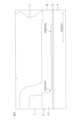
図1は、本開示の第1実施形態に係る窒化物半導体装置の構成を説明するための断面図である。Figure 1 is a cross-sectional view illustrating the configuration of a nitride semiconductor device according to the first embodiment of the present disclosure.
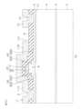
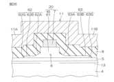
窒化物半導体装置1は、基板2と、基板2の表面に形成されたバッファ層3と、バッファ層3上にエピタキシャル成長された第1窒化物半導体層4と、第1窒化物半導体層4上にエピタキシャル成長された第2窒化物半導体層5とを含む。さらに、窒化物半導体装置1は、第2窒化物半導体層5上に選択的に形成された第3窒化物半導体層6と、第3窒化物半導体層6上に形成されたゲート電極7とを含む。The
さらに、この窒化物半導体装置1は、第2窒化物半導体層5、第3窒化物半導体層6およびゲート電極7を覆うパッシベーション膜8を含む。さらに、この窒化物半導体装置1は、パッシベーション膜8に形成されたソースコンタクトホール(第1開口部)9およびドレインコンタクトホール(第2開口部)10を通って第2窒化物半導体層5に接触するソース電極11およびドレイン電極12を含む。ソース電極11およびドレイン電極12は、ゲート電極7を挟んで対向配置されている。The
ソース電極11は、ソース主電極部11Aと、ゲート部20を覆うソースフィールドプレート部11Bとからなる。この実施形態では、ソース主電極部11Aとは、平面視において、ソース電極11の全領域のうち、ソースコンタクトホール9の輪郭に囲まれた領域およびその周辺領域からなる領域をいうものとする。ソースフィールドプレート部11Bは、ソース電極11の全領域のうち、ソース主電極部11A以外の部分をいう。ソースフィールドプレート部11Bは、ゲート電極7と後述するドレイン電極12との間に配置された部分を有している。ソースフィールドプレート部11Bのドレイン電極側端11Cは、平面視において、ドレインコンタクトホール10とゲート電極7(後述する第3窒化物半導体層6のリッジ部61)との間に配置されている。ソースフィールドプレート部11Bは、ゲート電圧が印加されていない状態(トランジスタオフ時)にゲート電極7とドレイン電極12との間の二次元電子ガス13に空乏層を広げることにより、ゲート電極7の端部への電界集中を緩和する。The
基板2は、例えば、低抵抗のシリコン基板であってもよい。低抵抗のシリコン基板は、例えば、0.001Ωmm~0.5Ωmm(より具体的には0.01Ωmm~0.1Ωmm程度)の電気抵抗率を有したp型基板でもよい。また、基板2は、低抵抗のシリコン基板の他、低抵抗のSiC基板、低抵抗のGaN基板等であってもよい。基板2の厚さは、半導体プロセス中においては、例えば650μm程度であり、チップ化する前段階において、300μm以下程度に研削される。基板2は、ソース電極11に電気的に接続されている。The
バッファ層3は、この実施形態では、複数の窒化物半導体膜を積層した多層バッファ層から構成されている。この実施形態では、バッファ層3は、基板2の表面に接するAlN膜からなる第1バッファ層(図示略)と、この第1バッファ層の表面(基板2とは反対側の表面)に積層されたグレーデッドAlGaN層からなるからなる第2バッファ層(図示略)とから構成されている。第1バッファ層の膜厚は、100nm~500nm程度である。第2バッファ層の膜厚は、Al組成が第1バッファ層側から順に75%、50%、25%の同膜厚のAlGaN層3層分を合計して300nm~1μm程度である。第2バッファ層を構成するグレーデッドAlGaN層の層数やそれぞれの膜厚比は異なってもよい。バッファ層3は、例えば、AlGaNの単膜、AlGaN/GaN超格子膜、AlN/AlGaN超格子膜、AlN/GaN超格子構造を有する膜などから構成されていてもよい。なお、バッファ層3を介したリーク電流を抑制するために、バッファ層3の一部に不純物を導入してバッファ層3の一部を半絶縁性にしてもよい。その場合、不純物はCまたはFeであり、不純物濃度は、例えば4×1016cm-2以上であることが望ましいた。 In this embodiment, the
第1窒化物半導体層4は、電子走行層を構成している。この実施形態では、第1窒化物半導体層4は、GaN層からなり、その厚さは0.5μm~2μm程度である。また、第1窒化物半導体層4を流れるリーク電流を抑制する目的で、表面領域以外には半絶縁性にするための不純物が導入されていてもよい。その場合、不純物の濃度は、4×1016cm-3以上であることが好ましい。また、不純物は、例えばCである。 The first
第2窒化物半導体層5は、電子供給層を構成している。第2窒化物半導体層5は、第1窒化物半導体層4よりもバンドギャップの大きい窒化物半導体から構成されている。具体的には、第2窒化物半導体層5は、第1窒化物半導体層4よりもAl組成の高い窒化物半導体から構成されている。窒化物半導体においては、Al組成が高いほどバッドギャップは大きくなる。この実施形態では、第2窒化物半導体層5は、AlxGa1-xN層(0.1<x≦0.3)からなる。第2窒化物半導体層5のAl組成は、20%以上30%以下であることが好ましく、24%以上25%以下であることがより好ましい。つまり、xは、0.2~0.3が好ましく、0.24~0.25がより好ましい。第2窒化物半導体層5の厚さは、8nm~20nmが好ましく、10.5nm~11.5nmがより好ましい。 The second
このように第1窒化物半導体層(電子走行層)4と第2窒化物半導体層(電子供給層)5とは、バンドギャップ(Al組成)の異なる窒化物半導体からなっており、それらの間には格子不整合が生じている。そして、第1窒化物半導体層4および第2窒化物半導体層5の自発分極と、それらの間の格子不整合に起因するピエゾ分極とによって、第1窒化物半導体層4と第2窒化物半導体層5との界面における第1窒化物半導体層4の伝導帯のエネルギーレベルはフェルミ準位よりも低くなる。これにより、第1窒化物半導体層4内には、第1窒化物半導体層4と第2窒化物半導体層5との界面に近い位置(例えば界面から数Å程度の距離)に、二次元電子ガス13が広がっている。The first nitride semiconductor layer (electron transport layer) 4 and the second nitride semiconductor layer (electron supply layer) 5 are made of nitride semiconductors with different band gaps (Al composition), and a lattice mismatch occurs between them. The spontaneous polarization of the first
第3窒化物半導体層6は、アクセプタ型不純物がドーピングされた窒化物半導体からなる。より具体的には、第3窒化物半導体層6は、アクセプタ型不純物がドーピングされたAlyGa1-yN(0≦y<1,y<x)層からなる。この実施形態では、第3窒化物半導体層6は、アクセプタ型不純物がドーピングされたGaN層(p型GaN層)からなっている。第3窒化物半導体層6の製造時において、アクセプタ型不純物がドーピングされたGaN層の成膜後に、p型化活性処理(例えば、窒素雰囲気内での加熱処理)を行わないことが好ましい。 The third
この実施形態では、アクセプタ型不純物は、Mg(マグネシウム)である。アクセプタ型不純物は、Zn(亜鉛)等のMg以外のアクセプタ型不純物であってもよい。In this embodiment, the acceptor-type impurity is Mg (magnesium). The acceptor-type impurity may be an acceptor-type impurity other than Mg, such as Zn (zinc).
第3窒化物半導体層6は、リッジ部31と延長部62,63とを含む。リッジ部31は、横断面が四角形状であり、上面の少なくとも幅中央部上にゲート電極が形成され、両側面各々のうち少なくとも上部が露出している。延長部62,63は、リッジ部61の側面の厚さ中間位置の下側部分から第2窒化物半導体層5の表面に沿ってリッジ部61の外方に延びている。The third
リッジ部61の両側面各々のうち、延長部62,63が形成されている部分は露出していない。言い換えれば、リッジ部61の両側面各々のうち、延長部62,63が形成されていない部分(上部)が露出している。延長部62,63は、平面視において、ソースコンタクトホール9とソースフィールドプレート部11Bのドレイン電極側端11Cとの間に配置されている。延長部62,63の膜厚は、リッジ部61の膜厚よりも薄い。この実施形態では、延長部62,63は、ソース側延長部(第1延長部)62と、ドレイン側延長部(第2延長部)63とを含む。The portions of both side surfaces of the
ソース側延長部62は、リッジ部61とソースコンタクトホール9との間に配置されている。ソース側延長部62は、リッジ部61のソース電極11側の側面の厚さ中間位置の下側部分からソースコンタクトホール9に向かって延びたテーパ部62Aと、テーパ部62Aのソース電極側端からソースコンタクトホール9に向かって延びた平坦部62Bとからなる。テーパ部62Aの表面は、ソースコンタクトホール9に向かって膜厚が漸減するような傾斜面に形成されている。第2窒化物半導体層5の表面に対するテーパ部62Aの表面の傾斜角(テーパ角)は、45度以下であることが好ましい。平坦部62Bの表面は、第2窒化物半導体層5の表面とほぼ平行であり、その膜厚はテーパ部62Aのソース電極側端の膜厚とほぼ等しい。テーパ部62Aは、本開示における「第1テーパ部」の一例である。The
ドレイン側延長部63は、リッジ部61とソースフィールドプレート部11Bのドレイン電極側端11Cとの間に配置されている。ドレイン側延長部63は、リッジ部61のドレイン電極12側の側面の厚さ中間位置の下側部分からドレインコンタクトホール10に向かって延びたテーパ部63Aと、テーパ部63Aのドレイン電極側端からドレインコンタクトホール10に向かって延びた平坦部63Bとからなる。テーパ部63Aの表面は、ドレインコンタクトホール10に向かって膜厚が漸減するような傾斜面に形成されている。第2窒化物半導体層5の表面に対するテーパ部63Aの表面の傾斜角(テーパ角)は、45度以下であることが好ましい。平坦部63Bの表面は、第2窒化物半導体層5の表面とほぼ平行であり、その膜厚はテーパ部63Aのドレイン電極側端の膜厚とほぼ等しい。テーパ部63Aは、本開示における「第1テーパ部」の一例である。The
リッジ部61の膜厚は、100nm以上であることが好ましい。リッジ部61の膜厚は、100nm以上140nm以下であることがより好ましく、110以上125nm以下であることがさらに好ましい。リッジ部61の膜厚が100nm以上140nm以下であれば、正方向のゲート最大定格電圧を高めることができるからである。この実施形態では、リッジ部61の膜厚は、110nm程度である。The thickness of the
延長部62,63の膜厚(詳しくは、平坦部62B,63Bの膜厚)は、25nm以下であることが好ましく、15nm以下であることがより好ましい。延長部62,63の膜厚は、リッジ部61の膜厚の1/5以下であることが好ましく、リッジ部61の膜厚の1/7以下であることが好ましい。The film thickness of the
ソース側延長部62のリッジ部61の幅方向の長さと、ドレイン側延長部63のリッジ部61の幅方向の長さとは、互いに異なっていてもよい。例えば、ドレイン側延長部63のリッジ部61の幅方向の長さが、ソース側延長部62のリッジ部61の幅方向の長さよりも長くてもよい。The widthwise length of the
リッジ部61の幅の長さは例えば500nm程度であり、ソース側延長部62の長さはリッジ部61の幅と同じ程度で、例えば150nm~450nm(リッジ部61の幅の0.3倍~0.9倍)である。ドレイン側延長部63の長さは、リッジ部61の幅と同じ程度か、好ましくはそれ以上である。ドレイン側延長部63の長さは、例えば350nm~1000nm(リッジ部61の幅の0.7倍~2.0倍)であり、好ましくは350nm~750nm(リッジ部61の幅の0.7倍~1.5倍)である。The width of the
また、リッジ部61の幅の長さは、ゲート電極7の幅とほぼ同じかまたは若干大きい。The width of the
延長部32,33のアクセプタ型不純物(Mg)の平均濃度が高すぎると、オン抵抗が増加する。このため、第3窒化物半導体層6直上のアクセプタ型不純物濃度を高くできない。そこで、第3窒化物半導体層6のアクセプタ型不純物の平均濃度を低くすると、閾値Vthが下がってしまう。オン抵抗を増加させることなく閾値Vthを上げるためには、第3窒化物半導体層6における延長部32,33よりも上層領域のアクセプタ型不純物の平均濃度を高くしたり、膜厚を厚くしたりする必要がある。 If the average concentration of the acceptor-type impurity (Mg) in the extensions 32 and 33 is too high, the on-resistance increases. For this reason, the acceptor-type impurity concentration directly above the third
このような観点から、延長部32,33のアクセプタ型不純物(Mg)の平均濃度は、リッジ部31のアクセプタ型不純物(Mg)の平均濃度よりも低くされている。これは、第2窒化物半導体層5上にエピタキシャル成長される、第3窒化物半導体層6の材料膜である第3半導体材料膜71(図2A参照)が、上面から下面に向かう方向の中央部から下面にかけて、アクセプタ型不純物濃度が漸減するような濃度プロファイルを有しているからである。From this perspective, the average concentration of the acceptor-type impurity (Mg) in the extensions 32, 33 is made lower than the average concentration of the acceptor-type impurity (Mg) in the ridge portion 31. This is because the third semiconductor material film 71 (see FIG. 2A), which is the material film of the third
また、第3窒化物半導体層6の下面から上方Xnmまでの領域を下層部とし、第3窒化物半導体層6の上面から下層部の上面までの領域を上層部とし、上層部の厚さをYnmとすると、次の第1条件および第2条件を満たすことが好ましい。Furthermore, assuming that the region from the lower surface of the third
第1条件:下層部の平均アクセプタ濃度が1×1019cm-3以下でありかつ上層部の平均アクセプタ濃度が1×1019cm-3よりも大きいという条件。 First condition: the average acceptor concentration in the lower layer is equal to or less than 1×1019 cm−3 and the average acceptor concentration in the upper layer is greater than 1×1019 cm−3 .
第2条件:5nm≦X≦40nmかつ70nm≦Y≦145nmかつ100nm≦X+Y≦150nmという条件。Second condition: 5 nm ≦ X ≦ 40 nm and 70 nm ≦ Y ≦ 145 nm and 100 nm ≦ X + Y ≦ 150 nm.
また、延長部62,63には、実質的にアクセプタ型不純物が含まれていないことが好ましい。実質的にアクセプタ型不純物が含まれていないとは、二次イオン質量分析(SIMS: Secondary Ion Mass Spectrometry)等の元素分析によってアクセプタ型不純物が検出されない程度を意味し、例えばアクセプタ型不純物が2×1015cm-3以下であることを意味する。 It is also preferable that the
延長部62,63にアクセプタ型不純物が実質的に含まれている場合には、アクセプタ型不純物が延長部62,63直下の第1窒化物半導体層4の伝導帯を押し上げるので、延長部62,63直下の二次元電子ガスのシートキャリア密度が低下する。これにより、オン抵抗が増加する。アクセプタ型不純物が実質的に含まれていない場合には、延長部62,63直下の二次元電子ガスのシートキャリア密度の低下を抑制できるので、オン抵抗を増加させることなく閾値Vthを大きくできるとともにゲート耐性を高くできる。 When the
アクセプタ型不純物がMgまたはZnである場合に、延長部62,63にアクセプタ型不純物が実質的に含まれないようにするためには、第3窒化物半導体層(p型GaN層)6の成膜時のアクセプタ型不純物流量条件を次のように変更すればよい。すなわち、第3窒化物半導体層6の成膜時に、延長部62,63が含まれる下層部のアクセプタ型不純物濃度がほぼ零となり、下層部の上の中層部のアクセプタ型不純物濃度が比較的低くなり、中層部の上の上層部のアクセプタ型不純物濃度が比較的高くなるように、アクセプタ型不純物流量条件を変更すればよい。When the acceptor-type impurity is Mg or Zn, in order to prevent the
なお、Znは下方への拡散が小さいので、アクセプタ型不純物がZnである場合には、前記中層部のアクセプタ型不純物濃度が、上層部のアクセプタ型不純物濃度と同様に高くなるように、アクセプタ型不純物流量条件を設定してもよい。In addition, since Zn has a small downward diffusion, when the acceptor-type impurity is Zn, the acceptor-type impurity flow conditions may be set so that the acceptor-type impurity concentration in the middle layer is as high as the acceptor-type impurity concentration in the upper layer.
なお、延長部62,63の下半部の領域に、実質的にアクセプタ型不純物が含まれていないようにしてもよい。この場合においても、延長部62,63全域に実質的にアクセプタ型不純物が含まれていない場合と同様の効果が期待できる。The lower half of the
リッジ部61と、リッジ部61上に形成されたゲート電極7とによってゲート部20が構成されている。ゲート部20は、ソースコンタクトホール9とドレインコンタクトホール10との間において、ソースコンタクトホール9寄りに偏って配置されている。The
リッジ部61は、ゲート部20の直下の領域において、第1窒化物半導体層4(電子走行層)と第2窒化物半導体層5(電子供給層)とで形成される界面の伝導帯を変化させ、ゲート電圧が印加されていない状態において、ゲート部20の直下の領域に二次元電子ガス13が発生しないようにするために設けられている。The
ゲート電極7の横断面は、矩形状である。ゲート電極7の幅は、リッジ部61の幅よりも狭い。ゲート電極7は、リッジ部61の上面の幅中間部上に形成されている。したがって、ゲート電極7の上面と、リッジ部61の一側部の上面との間に段差が形成されているとともに、ゲート電極7の上面と、リッジ部61の他側部の上面との間に段差が形成されている。また、平面視において、ゲート電極7の両側縁は、リッジ部61の対応する側縁よりも内方に後退している。The cross section of the
この実施形態では、ゲート電極7は、リッジ部61の上面にショットキー接触している。ゲート電極7は、例えば、TiNからなる。ゲート電極7の膜厚は、60nm以上200nm以下が好ましく、140nm以上150以下がより好ましい。ゲート電極7は、Ti膜、TiN膜およびTiW膜のうちのいずれか1つの単膜またはそれらの2以上の任意の組み合わせからなる複合膜から構成されてもよい。In this embodiment, the
パッシベーション膜8は、第2窒化物半導体層5の露出面(コンタクトホール9,10が臨んでいる領域を除く)、第3窒化物半導体層6の露出面およびゲート電極7の露出面を覆っている。この結果、ゲート部20の側面および表面は、パッシベーション膜8によって覆われる。パッシベーション膜8の膜厚は、50nm以上200nm以下が好ましく、85nm以上105nm以下がより好ましい。この実施形態では、パッシベーション膜8は、SiN膜からなる。パッシベーション膜8は、SiN膜、SiO2膜、SiON膜、Al2O3膜、AlN膜およびAlON膜のうちのいずれか1つの単膜またはそれらの2以上の任意の組み合わせからなる複合膜から構成されてもよい。 The
ソース電極11およびドレイン電極12は、例えば、第2窒化物半導体層5に接触する第1金属層(オーミックメタル層)と、第1金属層に積層された第2金属層(主電極メタル層)と、第2金属層に積層された第3金属層(密着層)と、第3金属層に積層された第4金属層(バリアメタル層)とからなる。第1金属層は、例えば、厚さが10nm~20nm程度のTi層である。第2金属層は、例えば、厚さが100nm~300nm程度のAl層である。第3金属層は、例えば、厚さが10nm~20nm程度のTi層である。第4金属層は、例えば、厚さが10nm~50nm程度のTiN層である。The
この窒化物半導体装置1では、第1窒化物半導体層4(電子走行層)上にバンドギャップ(Al組成)の異なる第2窒化物半導体層5(電子供給層)が形成されてヘテロ接合が形成されている。これにより、第1窒化物半導体層4と第2窒化物半導体層5との界面付近の第1窒化物半導体層4内に二次元電子ガス13が形成され、この二次元電子ガス13をチャネルとして利用したHEMT(トランジスタ)が形成されている。ゲート電極22は、第3窒化物半導体層6(詳しくはリッジ部61)を挟んで、第2窒化物半導体層5に対向している。In this
ゲート電極7の下方においては、p型GaN層からなるリッジ部61に含まれるアクセプタによって、第1窒化物半導体層4および第2窒化物半導体層5のエネルギーレベルが引き上げられる。このため、第1窒化物半導体層4と第2窒化物半導体層5との間のヘテロ接合界面における伝導帯のエネルギーレベルはフェルミ準位よりも大きくなる。したがって、ゲート電極7(ゲート部20)の直下では、第1窒化物半導体層4および第2窒化物半導体層5の自発分極ならびにそれらの格子不整合によるピエゾ分極に起因する二次元電子ガス13が形成されない。Below the
よって、ゲート電極7にバイアスを印加していないとき(ゼロバイアス時)には、二次元電子ガス13によるチャネルはゲート電極7の直下で遮断されている。こうして、ノーマリーオフ型のHEMTが実現されている。ゲート電極7に適切なオン電圧(例えば5V)を印加すると、ゲート電極7の直下の第1窒化物半導体層4内にチャネルが誘起され、ゲート電極7の両側の二次元電子ガス13が接続される。これにより、ソース-ドレイン間が導通する。Therefore, when no bias is applied to the gate electrode 7 (zero bias), the channel formed by the two-
使用に際しては、たとえば、ソース電極11とドレイン電極12との間に、ドレイン電極12側が正となる所定の電圧(例えば50V~100V)が印加される。その状態で、ゲート電極7に対して、ソース電極11を基準電位(0V)として、オフ電圧(0V)またはオン電圧(5V)が印加される。When in use, for example, a predetermined voltage (e.g., 50 V to 100 V) is applied between the
なお、図26に示すように、各延長部62,63は、先端部にテーパ部62G,63Gを有していてもよい。図26の例では、ソース側延長部62は、延長部62の基端側のテーパ部62Aと、延長部62の先端側のテーパ部62Gと、それらの間の平坦部62Bとからなる。同様に、ドレイン側延長部63は、延長部63の基端側のテーパ部63Aと、延長部63の先端側のテーパ部63Gと、それらの間の平坦部63Bとからなる。As shown in FIG. 26, each
テーパ部62Gおよびテーパ部63Gの表面は、それぞれソース側延長部32およびドレイン側延長部33の先端に向かって膜厚が漸減するような傾斜面に形成されている。第2窒化物半導体層5の表面に対するテーパ部62G,63Gの表面の傾斜角(テーパ角)は、30度以上80度以下であることが好ましい。テーパ部62G,63Gは、本開示の「第2テーパ部」の一例である。The surfaces of the tapered
このような構成では、延長部62,63の先端部(テーパ部62G,63Gの下縁)と第2窒化物半導体層5との間の隅部において、パッシベーション膜8が急峻な角部を有しないので、角部への応力集中を抑制され、局所的な二次元電子ガスの増加による耐圧低下を抑制できる。In this configuration, the
また、延長部62,63にアクセプタ型不純物が含まれている場合には、延長部62,63先端部内の二次元電子ガスのシートキャリア密度が横方向(リツジ部31の幅方向)に連続的に変化する構造となり、トランジスタオフ時の電解集中緩和が抑制され、耐圧が向上する。In addition, when the
図2A~図2Hは、前述の窒化物半導体装置1の製造方法の一例を説明するための断面図であり、製造方法における複数の段階における断面構造が示されている。Figures 2A to 2H are cross-sectional views for explaining an example of a method for manufacturing the
まず、図2Aに示すように、MOCVD(Metal Organic Chemical Vapor Deposition)法によって、基板2上に、バッファ層3、第1窒化物半導体層(電子走行層)4および第2窒化物半導体層(電子供給層)5および第3窒化物半導体層6の材料膜である第3半導体材料膜71がエピタキシャル成長される。First, as shown in FIG. 2A, a third
次に、図2Bに示すように、例えばスパッタ法によって、露出した表面全体を覆うように、ゲート電極7の材料膜であるゲート電極膜72が形成される。Next, as shown in FIG. 2B, a
次に、図2Cに示すように、ゲート電極膜72上に、第1絶縁膜(例えばSiO2膜)73が形成される。そして、例えばドライエッチングによって、ゲート電極膜72表面におけるゲート電極作成予定領域上の第1絶縁膜73を残して、第1絶縁膜73が選択的に除去される。そして、第1絶縁膜73をマスクとしたドライエッチングにより、ゲート電極膜72がパターニングされる。これにより、ゲート電極7が形成される。 2C, a first insulating film (e.g., aSiO2 film) 73 is formed on the
この後、例えばプラズマ化学的蒸着法(PECVD法)によって、露出した表面全体を覆うように第2絶縁膜(例えばSiO2膜)74が形成される。そして、例えばドライエッチングにより、第2絶縁膜74がエッチバックされることにより、ゲート電極7および第1絶縁膜73の側面を覆う第2絶縁膜74が形成される。 Thereafter, a second insulating film (e.g., aSiO2 film) 74 is formed so as to cover the entire exposed surface by, for example, a plasma enhanced chemical vapor deposition (PECVD) method. Then, the second insulating
次に、図2Dに示すように、第1絶縁膜73および第2絶縁膜74をマスクとした第1ドライエッチング工程により、第3半導体材料膜71が、所定の第1指定領域において所定の第1深さ分エッチングされる。具体的には、第3半導体材料膜71における第1および第2絶縁膜73,74によって覆われていない領域(第1指定領域)が、所定の第1深さ分エッチングされる。第1深さは、第3半導体材料膜71の厚さから、延長部62,63の平坦部62B,63Bの厚さを差し引いた厚さとほぼ等しい。Next, as shown in FIG. 2D, the third
第1ドライエッチング工程後の第3半導体材料膜71は、第1および第2絶縁膜73,74の直下のリッジ部61と、リッジ部61以外の薄膜部82,83とから構成される。薄膜部82,83は、リッジ部61の一方の側面の厚さ中間位置の下側部分から外方に突出したソース側薄膜部82と、リッジ部61の他方の側面の厚さ中間位置の下側部分から外方に突出したドレイン側薄膜部83とからなる。The third
ソース側薄膜部82は、リッジ部61の一方の側面の厚さ中間位置の下側部分から外方に向かって延びかつ厚さが外方に向かって漸減するテーパ部82Aと、テーパ部82Aの突出端から外方に向かって延びかつ厚さがほぼ一定の平坦部82Bとからなる。ドレイン側薄膜部83は、リッジ部61の他方の側面の厚さ中間位置の下側部分から外方に向かって延びかつ厚さが外方に向かって漸減するテーパ部83Aと、テーパ部83Aの突出端から外方に向かって延びかつ厚さがほぼ一定の平坦部83Bとからなる。The source-side thin-
第1ドライエッチング工程は、構造物近傍のエッチング速度が遅い条件(例えばICPを用いたエッチングにて被エッチング対象物側に掛けられたBiasが30W以下)で、干渉光を使ったエンドポイントモニタによるエッチング膜厚管理を適用しながら1ステップ形成されていてよい。また、第1ドライエッチング工程は、第3半導体材料膜71の表面からテーパ部82A,83Aの上端位置までの第3半導体材料膜71をエッチングする前工程と、テーパ部82A,83Aの上端位置から平坦部82B,83Bの上面までの第3半導体材料膜71をエッチングする後工程からなっていてもよい。この場合には、前工程と後工程との間において、例えば、エッチングガスの量やプラズマの電力が変更されることにより、エッチング速度が変更される。具体的には、後工程のエッチング速度が、前工程のエッチング速度よりも遅くされる。The first dry etching process may be formed in one step under conditions where the etching rate near the structure is slow (for example, the bias applied to the etched object side in the etching using ICP is 30 W or less), while applying etching film thickness management by an end point monitor using interference light. The first dry etching process may also be composed of a pre-process of etching the third
次に、図2Eに示すように、第3窒化物半導体層6の形成予定領域を覆うレジスト(図示略)をマスクとした第2ドライエッチング工程により、第3半導体材料膜71が、所定の第2指定領域において所定の第2深さ分エッチングされる。具体的には、第3半導体材料膜71におけるレジストマスクによって覆われていない領域(第2指定領域)が、所定の第2深さ分エッチングされる。第2ドライエッチング工程においては、第3半導体材料膜71と第2窒化物半導体層5の間で選択比が10以上の条件(例えば、Cl2にO2またはCF4などを混合したガスを使用する)で、第3半導体材料膜71がエッチングされる。第2深さは、延長部62,63の平坦部62B,63Bの厚さとほぼ等しい。 2E, the third
第2ドライエッチング工程後の第3半導体材料膜71は、第1および第2絶縁膜73,74の直下のリッジ部61と、リッジ部61以外の延長部62,63とからなる。前述したように、延長部62,63は、ソース側延長部62とドレイン側延長部63とを含む。ソース側延長部62は、テーパ部62Aと平坦部62Bとからなる。ドレイン側延長部63は、テーパ部63Aと平坦部63Bとからなる。The third
このようにして、リッジ部61と延長部62,63とからなる第3窒化物半導体層6が得られる。また、リッジ部61と、リッジ部61上面の幅中間部上に形成されたゲート電極7とからなるゲート部20が得られる。In this way, a third
次に、図2Fに示すように、ウエットエッチングにより、第1および第2絶縁膜73,74が除去される。この後、露出した表面全体を覆うように、パッシベーション膜8が形成される。パッシベーション膜8は例えばSiNからなる。Next, as shown in FIG. 2F, the first and second insulating
次に、図2Gに示すように、パッシベーション膜8に、ソースコンタクトホール9およびドレインコンタクトホール10が形成される。Next, as shown in FIG. 2G, a
次に、図2Hに示すように、露出した表面全体を覆うようにソース・ドレイン電極膜76が形成される。Next, as shown in FIG. 2H, a source/
最後に、フォトリソグラフィおよびエッチングによってソース・ドレイン電極膜76がパターニングされることにより、第2窒化物半導体層5に接触するソース電極11およびドレイン電極12が形成される。こうして、図1に示すような構造の窒化物半導体装置1が得られる。Finally, the source/
なお、図2Dの工程に代えて、図3に示される工程を用いてもよい。In addition, the process shown in FIG. 3 may be used instead of the process shown in FIG. 2D.
すなわち、図2Cの工程が終了すると、図3に示すように、第3窒化物半導体層6の形成予定領域を覆うレジスト(図示略)をマスクとした第1ドライエッチング工程により、第3半導体材料膜71が、所定の第1指定領域において所定の第1深さ分エッチングされる。具体的には、レジストマスクによって覆われていない領域(第1指定領域)が、所定の第1深さ分エッチングされる。第1深さは、例えば、第3半導体材料膜71の厚さ(リッジ部61の厚さ)の1/3程度の深さである。That is, when the process of FIG. 2C is completed, as shown in FIG. 3, a first dry etching process is performed using a resist (not shown) that covers the region where the third
第1ドライエッチング工程後の第3半導体材料膜71は、第1絶縁膜73および第2絶縁膜74の直下の厚膜部91と、厚膜部91以外の薄膜部92とからなる。After the first dry etching process, the third
この後、第1絶縁膜73および第2絶縁膜74をマスクとした第2ドライエッチング工程により、第3半導体材料膜71が、所定の第2指定領域において所定の第2深さ分エッチングされる。具体的には、第3半導体材料膜71における第1および第2絶縁膜73,74によって覆われていない領域(第2指定領域)が、所定の第2深さ分エッチングされる。第2深さは、例えば、図3の厚膜部91の厚さとほぼ等しい深さである。Then, the third
第2ドライエッチング工程後の第3半導体材料膜71は、前述の図2Eに示されるように、第1および第2絶縁膜73,74の直下のリッジ部61と、リッジ部61以外の延長部62,63とからなる。前述したように、延長部62,63は、ソース側延長部62とドレイン側延長部63とを含む。ソース側延長部62は、テーパ部62Aと平坦部62Bとからなる。ドレイン側延長部63は、テーパ部63Aと平坦部63Bとからなる。As shown in FIG. 2E, the third
このようにして、リッジ部61と延長部62,63とからなる第3窒化物半導体層6が得られる。また、リッジ部61と、リッジ部61上面の幅中間部上に形成されたゲート電極7とからなるゲート部20が得られる。In this way, a third
なお、第2ドライエッチング工程は、構造物近傍のエッチング速度が遅い条件(例えばICPを用いたエッチングにて被エッチング対象物側に掛けられたBiasが30W以下)で1ステップ形成されていてよい。また、第2ドライエッチング工程は、第3半導体材料膜71の表面からテーパ部62A,63Aの上端までの第3半導体材料膜71をエッチングする前工程と、テーパ部62A,62Aの上端から第2窒化物半導体層5の表面までの第3半導体材料膜71をエッチングする後工程からなっていてもよい。この場合には、前工程と後工程との間において、例えば、エッチングガスの量やプラズマの電力が変更されることにより、エッチング速度が変更される。具体的には、後工程のエッチング速度が、前工程のエッチング速度よりも遅くされる。図3の工程が終了すると、前述の図2Fの工程が行われる。The second dry etching process may be formed in one step under conditions where the etching rate near the structure is slow (for example, the bias applied to the etched object side in the etching using ICP is 30 W or less). The second dry etching process may also be composed of a pre-process of etching the third
図4は、図1の窒化物半導体装置におけるドレイン側延長部63およびその近傍のSTEM(Scanning Tunneling Electron Microscopy)顕微鏡写真を模写した断面図である。図4から、ドレイン側延長部63(より詳しくは平坦部63B)が10nm程度の膜厚で形成されていることが確認できる。Figure 4 is a cross-sectional view of the
以下において、図1の窒化物半導体装置1において、延長部62,63が省略された構成を、第1比較例ということにする。また、特許文献2の図8に示されるように、AlGaN電子供給層上において、リッジ形状の厚膜のp型GaN層が形成されている領域以外の領域全域に、薄膜のp型GaN層が形成された構造を第2比較例ということにする。In the following, a configuration in which the
図1に示される第1実施形態に係る窒化物半導体装置1では、第3窒化物半導体層6が、リッジ部61の側面の厚さ中間位置の下側部分から外方に延びた延長部62,63を有している。これにより、第1実施形態に係る窒化物半導体装置1では、第1比較例に比べてゲートリーク電流を低減してゲート耐圧を伸ばしつつ、電流コラプスを抑制でき、第2比較例に比べて耐圧の低下を抑制できる。これらの効果につき、以下、詳しく説明する。In the
まず、図5を参照して、ゲートリーク電流が増大するメカニズムについて説明する。図5は、第1比較例のエネルギー分布を示すエネルギーバンド図である。図5において、Ecは、伝導帯のエネルギーレベルであり、Evは価電子帯のエネルギーレベルである。First, the mechanism by which the gate leakage current increases will be described with reference to FIG. 5. FIG. 5 is an energy band diagram showing the energy distribution of the first comparative example. In FIG. 5, Ec is the energy level of the conduction band, and Ev is the energy level of the valence band.
図5に示すように、トランジスタオフ時には、伝導帯のエネルギーレベルEcからわかるように、GaNからなる第1窒化物半導体層4とAlGaNからなる第2窒化物半導体層5との界面において、伝導帯内に電子に対する障壁が形成されている。これにより、第1窒化物半導体層4からp型GaNからなる第3窒化物半導体層6への電子の移動が抑制されるので、ゲートリーク電流は大きくならない。As shown in FIG. 5, when the transistor is off, as can be seen from the energy level Ec of the conduction band, a barrier against electrons is formed in the conduction band at the interface between the first
ゲート電極7とソース電極11との間にゲート-ソース間電圧Vgsが印加されると、ゲート電極7からp型GaNからなる第3窒化物半導体層6内にホールが注入される。価電子帯のエネルギーレベルEvからわかるように、第3窒化物半導体層6と第2窒化物半導体層5との界面にホールに対する障壁(価電子帯障壁)が形成されているため、第3窒化物半導体層6内に注入されたホールが当該界面に蓄積される。そうすると、図5に破線で示すように第2窒化物半導体層5の電子に対する障壁(伝導帯障壁)が下がるので、第1窒化物半導体層4から第3窒化物半導体層6へ電子が移動しやすくなる。これにより、ゲートリーク電流が増大する。 When a gate-source voltageVgs is applied between the
本実施形態では、第3窒化物半導体層6は延長部62,63を有しているため、第3窒化物半導体層6と第2窒化物半導体層5との界面の面積が、第1比較例に比べて大きくなる。これにより、本実施形態では、第3窒化物半導体層6と第2窒化物半導体層5との界面に蓄積されるホールの密度が第1比較例に比べて低くなる。これにより、本実施形態では、第2窒化物半導体層5の伝導帯障壁の低下が第1比較例に比べて抑制されるので、第1比較例に比べてゲートリーク電流を低減できる。In this embodiment, since the third
図6は、本実施形態および第1比較例それぞれのゲート-ソース間電圧Vgsに対するゲートリーク電流Igの測定結果を示すグラフである。図6において、実線は本実施形態に対する測定結果を示し、破線は第1比較例に対する測定結果を示している。 6 is a graph showing the measurement results of the gate leakage currentIg versus the gate-source voltageVgs for this embodiment and the first comparative example. In Fig. 6, the solid line shows the measurement results for this embodiment, and the dashed line shows the measurement results for the first comparative example.
図6のグラフから、本実施形態では、ゲート-ソース間電圧Vgsが3V以上の範囲において、第1比較例に比べて、ゲートリーク電流Igが小さくなっていることかわかる。 From the graph of FIG. 6, it can be seen that in this embodiment, the gate leakage current Ig is smaller than that in the first comparative example when the gate-source voltage Vgs is in the range of 3 V or more.
図7は、本実施形態および第1比較例それぞれのゲート-ソース間電圧Vgsに対するTDDB(Time Dependent Dielectric Breakdown)試験から得た破壊時間(Time to Breakdown)の測定結果を示すグラフである。図7において、実線は本実施形態に対する測定結果を示し、破線は第1比較例に対する測定結果を示している。 7 is a graph showing the measurement results of the time to breakdown obtained from a time dependent dielectric breakdown (TDDB) test for the gate-source voltageVgs of the present embodiment and the first comparative example. In FIG. 7, the solid line shows the measurement results for the present embodiment, and the dashed line shows the measurement results for the first comparative example.
図7のグラフから、本実施形態では、第1比較例に比べて、ゲート-ソース間電圧Vgsに対する寿命視点の耐性も2V程度向上していることがわかる。 From the graph of FIG. 7, it can be seen that in this embodiment, the resistance to the gate-source voltageVgs from the viewpoint of life is improved by about 2 V compared to the first comparative example.
一方、電流コラプスは、トランジスタオフ時において、ドレインーソース間に印加される電圧によってAlGaN電子供給層表面やGaN電子走行層内にトラップされた電子が二次元電子ガス13を阻害し、オン抵抗を増大させる現象である。On the other hand, current collapse is a phenomenon in which, when the transistor is off, electrons trapped on the surface of the AlGaN electron supply layer or in the GaN electron transit layer due to the voltage applied between the drain and source inhibit the two-
本実施形態では、第3窒化物半導体層6が延長部62,63を有しているので、ゲート部近傍のエッチング表面(本実施形態では延長部62,63の表面)と二次元電子ガス13との間の物理的距離を、比較例に比べて大きくすることができる。なお、第1比較例のゲート部近傍のエッチング表面は、第2窒化物半導体層5の表面となる。これにより、ゲート部近傍のエッチング表面にトラップされた電子が二次元電子ガス13を阻害するのを抑制できるので、電流コラプスが抑制される。In this embodiment, since the third
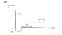
本実施形態および第1比較例に対して、複数のドレイン-ソース間電圧Vds毎に、電流コラプスの大きさの指標であるコラプスファクターCFを測定した。所定のドレイン-ソース間電圧Vdsに対するコラプスファクターCFは、ストレス印加前のオン抵抗をRon(initial)とし、ドレインストレス印加後のオン抵抗をRon(after stress)とすると、次式(1)によって表される。 The collapse factor CF, which is an index of the magnitude of current collapse, was measured for each of a plurality of drain-source voltagesVds for this embodiment and the first comparative example. The collapse factor CF for a given drain-source voltageVds is expressed by the following formula (1), where the on-resistance before application of stress is Ron (initial) and the on-resistance after application of drain stress is Ron (after stress) .
CF=Ron(after stress)/Ron(initial) …(1)
コラプスファクターCFは、CFが小さいほど電流コラプスが小さいことを示す指標である。 CF=Ron(after stress) /Ron(initial) …(1)
The collapse factor CF is an index indicating that the smaller the CF, the smaller the current collapse.
所定のドレイン-ソース間電圧Vdsに対するドレインストレス印加後のオン抵抗は、次のようにして測定される。すなわち、図8を参照して、ソース電極11とドレイン電極12との間に当該所定のドレイン-ソース間電圧Vdsを所定の第1時間T1(例えば、1sec~2sec)だけ印加した後、ドレイン-ソース間電圧Vdsを零にする。そして、所定時間T2(例えば100μsec)が経過すると、ソース電極11とドレイン電極12との間に当該所定のドレイン-ソース間電圧Vdsを印加すると同時にソース電極11とゲート電極7との間に所定のゲート-ソース間電圧Vgsを印加する。この後の期間T3内に、ドレインストレス印加後のオン抵抗Ron(after stress)を測定する。ストレス印加前のオン抵抗Ron(initial))は、ストレス印加前に測定される。 The on-resistance after application of drain stress for a given drain-source voltage Vds is measured as follows. That is, referring to FIG. 8, the given drain-source voltage Vds is applied between the
図9は、本実施形態および第1比較例それぞれのドレイン-ソース間電圧Vdsに対するコラプスファクターCFの測定結果を示すグラフである。図9において、実線は本実施形態に対する測定結果を示し、破線は第1比較例に対する測定結果を示している。 9 is a graph showing the measurement results of the collapse factor CF versus the drain-source voltageVds for the present embodiment and the first comparative example. In FIG. 9, the solid line shows the measurement results for the present embodiment, and the dashed line shows the measurement results for the first comparative example.
図9のグラフから、本実施形態では、第1比較例に比べて、コラプスファクターCFが小さくなっていることかわかる。つまり、本実施形態では、第1比較例に比べて、電流コラプスが抑制されていることがわかる。From the graph in FIG. 9, it can be seen that in this embodiment, the collapse factor CF is smaller than in the first comparative example. In other words, it can be seen that in this embodiment, current collapse is suppressed compared to the first comparative example.
第2比較例では、ソースフィールドプレートによって、ゲート-ドレイン間の二次元電子ガスを空乏化させようとした場合、次のような問題が生じる。すなわち、ソースフィールドプレートのドレイン電極側端と二次元電子ガスとの間に、薄膜のp型GaN層が存在しているために、ソースフィールドプレートによって二次元電子ガスに空乏層を効果的に広げられず、耐圧が低下する。In the second comparative example, when attempting to deplete the two-dimensional electron gas between the gate and drain using a source field plate, the following problem occurs. That is, because a thin p-type GaN layer exists between the drain electrode side end of the source field plate and the two-dimensional electron gas, the source field plate cannot effectively expand the depletion layer into the two-dimensional electron gas, and the breakdown voltage decreases.
これに対し、本実施形態では、ドレイン側延長部63のドレイン電極側端は、平面視において、リッジ部61のドレイン電極12側の側面とソースフィールドプレート部11Bのドレイン電極側端12Cとの間に形成されている。言い換えれば、ソースフィールドプレート部11Bのドレイン電極側端12Cの真下には、延長部62,63は存在しない。これにより、ソースフィールドプレート部11Bによって、二次元電子ガスに空乏層を効果的に広げることができるので、第2比較例に比べて耐圧の低下を抑制できる。In contrast, in this embodiment, the drain electrode side end of the
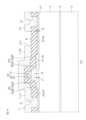
図10は、本開示の第2実施形態に係る窒化物半導体装置の構成を説明するための断面図である。図10において、前述の図1の各部に対応する部分には、図1と同じ符号を付して示す。Figure 10 is a cross-sectional view for explaining the configuration of a nitride semiconductor device according to a second embodiment of the present disclosure. In Figure 10, parts corresponding to those in Figure 1 described above are denoted by the same reference numerals as in Figure 1.
第2実施形態に係る窒化物半導体装置1Aでは、図1の窒化物半導体装置1のテーパ部62Aおよび63Aに相当する部分62Cおよび63Cが、それぞれ図1の窒化物半導体装置1の平坦部62Bおよび63Bに相当する部分62Dおよび63Dよりも膜厚が厚い第1平坦部62Cおよび63Cに形成されている点で、第1実施形態と異なっている。The
つまり、第2実施形態に係る窒化物半導体装置1Aでは、ソース側延長部62は、リッジ部61のソース電極11側の側面の厚さ中間位置の下側部分からソースコンタクトホール9に向かって延びた断面矩形状の第1平坦部(厚膜部)62Cと、第1平坦部62Cのソース電極11側の側面の厚さ中間位置の下側部分からソースコンタクトホール9に向かって延びた断面矩形状の第2平坦部(薄膜部)62Dとからなる。In other words, in the
また、ドレイン側延長部63は、リッジ部61のドレイン電極12側の側面の厚さ中間位置の下側部分からドレインコンタクトホール10に向かって延びた断面矩形状の第1平坦部(厚膜部)63Cと、第1平坦部63Cのドレイン電極12側の側面の厚さ中間位置の下側部分からドレインコンタクトホール10に向かって延びた断面矩形状の第2平坦部(薄膜部)63Dとからなる。The
図11A~図11Cは、第2実施形態に係る窒化物半導体装置1Aの製造方法の一例を説明するための断面図であり、製造方法における複数の段階における断面構造が示されている。Figures 11A to 11C are cross-sectional views for explaining an example of a method for manufacturing a
第2実施形態に係る窒化物半導体装置1Aを製造する場合には、まず、前述した図2A~図2Cに示される工程が実施される。ここでは、第3半導体材料膜71の厚さは、110nm程度であるとする。図2Cの工程が終了すると、図11Aに示すように、第1絶縁膜73および第2絶縁膜74をマスクとした第1ドライエッチング工程により、第3半導体材料膜71におけるマスクによって覆われていない領域(第1指定領域)の厚さが30nm程度となるまで、第3半導体材料膜71がエッチングされる。言い換えれば、第1指定領域が所定の第1深さ分だけ、エッチングされる。第1深さは、80nm(=110nm-30nm)程度である。第1ドライエッチング工程後の第3半導体材料膜71は、第1絶縁膜73および第2絶縁膜74の直下の厚膜部91と、厚膜部91以外の薄膜部92とからなる。When manufacturing the
次に、第1絶縁膜73および第2絶縁膜74を除去した後、原子間力顕微鏡(AFM)によるエッチング段差測定結果から、第1指定領域の厚さを算出する。Next, after removing the first insulating
次に、図11Bに示すように、リッジ部61および第1平坦部62C,63Cの形成予定領域を覆うレジスト(図示略)をマスクとしたドライエッチング工程(以下、「第3エッチング工程」という。)により、第3半導体材料膜71におけるレジストマスクによって覆われていない領域(第3指定領域)の厚さが10nm程度となるまで、第3半導体材料膜71がエッチングされる。言い換えれば、第3指定領域が所定の第3深さ分だけ、エッチングされる。第3深さは、20nm(=30nm-10nm)程度である。第3エッチング工程後の第3半導体材料膜71は、第1絶縁膜73および第2絶縁膜74の直下の厚膜部91と、厚膜部91の両側の第1薄膜部92と、両第1薄膜部92の外側の第2薄膜部93とからなる。11B, the third
次に、図11Cに示すように、第3窒化物半導体層6の形成領域を覆うレジスト(図示略)をマスクとしたドライエッチング工程(以下、「第2エッチング工程」という。)により、第3半導体材料膜71におけるレジストマスクによって覆われていない領域(第2指定領域)が除去されるまで、第3半導体材料膜71がエッチングされる。言い換えれば、第2指定領域が所定の第2深さ分だけ、エッチングされる。第2深さは、例えば、第2平坦部62D,63Dの厚さとほぼ等しい。第2エッチング工程後の第3半導体材料膜71は、リッジ部61と、リッジ部61以外の延長部62,63とからなる。11C, the third
この後、前述した図2F以降と同様な工程が実施されることにより、図10に示すような構造の窒化物半導体装置1Aが得られる。After this, the same processes as those shown in FIG. 2F and onwards are carried out to obtain a
図12は、本開示の第3実施形態に係る窒化物半導体装置の構成を説明するための断面図である。図12において、前述の図1の各部に対応する部分には、図1と同じ符号を付して示す。Figure 12 is a cross-sectional view for explaining the configuration of a nitride semiconductor device according to a third embodiment of the present disclosure. In Figure 12, parts corresponding to those in Figure 1 described above are denoted by the same reference numerals as in Figure 1.
第3実施形態に係る窒化物半導体装置1Bでは、第3窒化物半導体層6は、ソース電極11(ソースコンタクトホール9)を挟むように配置された離間部68およびドレイン電極12(ドレインコンタクトホール10)を挟むように配置された離間部68を有している。これらの離間部68は、リッジ部61に接続されておらず、リッジ部61の膜厚よりも薄い膜厚を有している。ソース電極11側の離間部68はソース電極11に接触し、ドレイン電極12側の離間部68はドレイン電極12に接触している。図12の例では、離間部68の膜厚は、延長部62,63(詳しくは、平坦部62B,63B)の膜厚とほぼ等しい。In the
第3実施形態に係る窒化物半導体装置1Bでは、第1実施形態に係る窒化物半導体装置1に比べて、トランジスタオフ時に、離間部68が設けられている領域において、エッチング表面にトラップされる電子の二次元電子ガスへの影響が低減する。これにより、第1実施形態に係る窒化物半導体装置1に比べて、電流コラプスをより効果的に抑制することができる。In the
図13は、本開示の第4実施形態に係る窒化物半導体装置の構成を説明するための断面図である。図13において、前述の図1の各部に対応する部分には、図1と同じ符号を付して示す。Figure 13 is a cross-sectional view for explaining the configuration of a nitride semiconductor device according to a fourth embodiment of the present disclosure. In Figure 13, parts corresponding to those in Figure 1 described above are denoted by the same reference numerals as in Figure 1.
第4実施形態に係る窒化物半導体装置1Cでは、第3窒化物半導体層6は、ドレイン側延長部63とドレインコンタクトホール10との間の領域に配置された離間部68を有している。この離間部68は、リッジ部61に接続されておらず、リッジ部61の膜厚よりも薄い膜厚を有している。離間部68の膜厚は、延長部62,63(詳しくは、平坦部62B,63B)の膜厚とほぼ等しい。In the
第4実施形態に係る窒化物半導体装置1Cでは、第3実施形態に係る窒化物半導体装置1Bと同様な効果が得られる。The
図14は、本開示の第5実施形態に係る窒化物半導体装置の構成を説明するための断面図である。図14において、前述の図1の各部に対応する部分には、図1と同じ符号を付して示す。Figure 14 is a cross-sectional view for explaining the configuration of a nitride semiconductor device according to a fifth embodiment of the present disclosure. In Figure 14, parts corresponding to those in Figure 1 described above are denoted by the same reference numerals as in Figure 1.
第5実施形態に係る窒化物半導体装置1Dでは、第2窒化物半導体層5における第3窒化物半導体層6(詳しくはリッジ部61および延長部62,63)が上方に存在する第1部分51の膜厚t1と、第2窒化物半導体層5おける第3窒化物半導体層6が上方に存在しない第2部分52の膜厚t2とが異なる。具体的には、第2部分52の膜厚t2は、第1部分51の膜厚t1よりも薄い。In the
第5実施形態に係る窒化物半導体装置1Dでは、ソースフィールドプレート部11Bのドレイン電極側端11Cの下方の第2窒化物半導体層5(第2部分52)の膜厚t2が、第1部分51の膜厚t1よりも薄い。ただし、ゲート電極近傍においては、第2窒化物半導体層5(第1部分51)の膜厚は、第2部分52の膜厚よりも厚い。In the
このため、第2部分52の膜厚t2が第1部分51の膜厚t1と同じ場合に比べて、ソースフィールドプレート部11Bのドレイン電極側端11Cの下方の二次元電子ガス13の密度を低減できる。これにより、トランジスタオフ時の電解集中を低減できるとともに電流コラプスを抑制することができる。As a result, the density of the two-
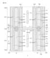
図15は、図1の窒化物半導体装置1のゲート電極、ソース電極、ドレイン電極および第3窒化物半導体層の平面パターンの一例を示す図解的な平面図である。図16は、図15のXVI-XVI線に沿う断面図である。図17は、図15のXVII-XVII線に沿う断面図である。図15~図17において、前述の図1の各部に対応する部分には、図1と同じ符号を付して示す。Figure 15 is a schematic plan view showing an example of the planar pattern of the gate electrode, source electrode, drain electrode and third nitride semiconductor layer of the
説明の便宜上、以下において、図15の紙面の左右方向を左右方向といい、図15の紙面の上下方向を前後方向という場合がある。また、図15の紙面の下側を前といい、図15の紙面の上側を後という場合がある。図15は、窒化物半導体装置1におけるゲート電極、ソース電極、ドレイン電極および第3窒化物半導体層の平面パターンの一部の領域を切り取って示したものであって、窒化物半導体装置1全体においては、このようなパターンが左右方向および前後方向にさらに連続している。以下において、図15に図示されている平面視での矩形の領域を、「切り取り領域」ということにする。For ease of explanation, in the following, the left-right direction of the paper surface of FIG. 15 may be referred to as the left-right direction, and the up-down direction of the paper surface of FIG. 15 may be referred to as the front-back direction. The lower side of the paper surface of FIG. 15 may be referred to as the front, and the upper side of the paper surface of FIG. 15 may be referred to as the back. FIG. 15 shows a cut-out region of a part of the planar pattern of the gate electrode, source electrode, drain electrode, and third nitride semiconductor layer in the
窒化物半導体装置1は、半導体積層構造と、半導体積層構造上に配置された電極メタル構造とを含む。半導体積層構造は、図16および図17に示すように、基板2と、基板2の表面に形成されたバッファ層3と、バッファ層3上にエピタキシャル成長された第1窒化物半導体層4と、第1窒化物半導体層4上にエピタキシャル成長された第2窒化物半導体層5と、第2窒化物半導体層5上にエピタキシャル成長された第3窒化物半導体層6を含む。The
窒化物半導体装置1は、切り取り領域において、前半領域と後半領域とが、切り取り領域の前後中央を通る左右に延びた直線に対して線対称となる構造を有している。そこで、まず、切り取り領域の前半領域の電極メタル構造につい説明する。The
切り取り領域の前半部分の電極メタル構造は、図15に示すように、複数のソース電極11、複数のゲート電極7およびドレイン電極12を含む。ソース電極11およびドレイン電極12は前後方向に延びている。As shown in FIG. 15, the electrode metal structure in the first half of the cutout region includes
ゲート電極7は、互いに平行に前後方向に延びた複数のゲート主電極部7Aと、これらのゲート主電極部7Aの対応する端部どうしをそれぞれ連結する2つのベース部7Bとを含む。図15では、明確化のため、ゲート電極7の領域に灰色を付して示している。The
1つのソース電極11は、平面視において、隣接する2つのゲート主電極部7Aの間に配置されたソース主電極部11Aと、ソース主電極部11Aの周囲のソースフィールドプレート部11B(図16参照)とからなる。ソースフィールドプレート部11Bは、図16に示すように、ソース主電極部11Aの両側に配置された一対のゲート主電極部7Aを覆っている。In a plan view, one
切り取り領域の前半領域には、1つのドレイン電極12しか描かれていないが、窒化物半導体装置1全体では、1つのソース電極11の両側のそれぞれに、ドレイン電極12が配置されている。隣り合うドレイン電極12およびソース主電極部11Aは、平面視において、ゲート主電極部7Aを挟んで互いに対向している。この実施形態では、ドレイン電極12の長さはソース主電極部11Aの長さよりも短く、左右方向から見て、ドレイン電極12の両端は、ソース主電極部11Aの対応する端よりもソース主電極部11Aの長さ中央側寄りに位置している。Although only one
ソース主電極部11A(S)、ゲート主電極部7A(G)およびドレイン電極12(D)は、左右方向にGSGDGSGDの順に周期的に配置されている。これにより、ソース主電極部11A(S)およびドレイン電極12(D)でゲート主電極部7A(G)を挟むことによって素子構造が構成されている。The source
切り取り領域の後半領域の電極メタル構造は、切り取り領域の前半領域の電極メタル構造と同様である。切り取り領域の前半領域におけるゲート電極7の後側のベース部7Bと、切り取り領域の後半領域におけるゲート電極7の前側のベース部7Bとは繋がっている。図15では、これらのベース部7Bを、1つのベース部7Bとして、取り扱っている。つまり、前半領域におけるゲート電極7と後半領域におけるゲート電極7とは一体的に形成されている。The electrode metal structure in the rear region of the cutout region is the same as the electrode metal structure in the front region of the cutout region. The
また、切り取り領域の前半領域におけるソース電極11のソースフィールドプレート部3Bの後端部と、窒化物半導体装置1の後半領域におけるソース電極11のソースフィールドプレート部3Bの前端部とは繋がっている。つまり、前半領域におけるソース電極11と後半領域におけるソース電極11とは一体的に形成されている。In addition, the rear end of the source field plate portion 3B of the
半導体積層構造上の表面の領域は、トランジスタ動作に寄与するアクティブ領域101と、トランジスタ動作に寄与しないノンアクティブ領域102とからなる。この実施形態では、アクティブ領域101とは、ゲート電極7にオン電圧が印加されているときに、ソース-ドレイン間に電流が流れる領域をいうものとする。The surface region on the semiconductor laminate structure consists of an
第3窒化物半導体層6は、平面視において、ゲート電極22とほぼ同じ形状を有している。具体的には、第3窒化物半導体層6は、互いに平行に縦方向に延びた複数のリッジ部61と、これらのリッジ部61の対応する端部どうしをそれぞれ連結する2つの連結部64(図17参照)と、リッジ部61の側面から外方に延びた延長部62,63とを含む。延長部62,63は、ソース側延長部62と、ドレイン側延長部63を含む。リッジ部61上に、ゲート電極7が形成されている。図15では、明確化のため、延長部62,63の領域にドットを付して示している。図16および図17においては、延長部62,63の断面形状が簡略化して描かれているため、それらは一様の厚さで描かれている。後述する図19においても同様である。The third
切り取り領域の前半部分におけるリッジ部61の後側の連結部64と、切り取り領域の後半部分におけるリッジ部61の前側の連結部64とは繋がっている。図15では、これらの連結部64を1つの連結部64として取り扱っている。The connecting
図15に示すように、ノンアクティブ領域102においても、リッジ部61の側面に延長部62,63が形成されていてもよい。また、図15および図17に示されるように、連結部64の側面にも、ドレイン側延長部63が形成されていてよい。ノンアクティブ領域102に形成された延長部62,63は、本開示の「ノンアクティブ延長部」の一例である。As shown in FIG. 15,
図18は、図1の窒化物半導体装置1のゲート電極、ソース電極、ドレイン電極および第3窒化物半導体層の平面パターンの他の例を示す図解的な平面図である。図19は、図18のXIX-XIX線に沿う断面図である。図18において、前述の図15の各部に対応する部分には、図15と同じ符号を付して示す。図19において、前述の図17の各部に対応する部分には、図17と同じ符号を付して示す。なお、前述の図16は、図18のXVI-XVI線に沿う断面図でもある。Figure 18 is a schematic plan view showing another example of the planar pattern of the gate electrode, source electrode, drain electrode and third nitride semiconductor layer of the
図18、図16および図19に示される窒化物半導体装置1は、図15、図16および図17に示される窒化物半導体装置1に比べて、第3窒化物半導体層6が、窒化物半導体装置1の前後中央部のノンアクティブ領域において、左右のドレイン側延長部63を接続する接続用延長部65を有している点にのみが異なっている。接続用延長部65は、本開示の「ノンアクティブ延長部」の一例である。The
図18に示される窒化物半導体装置1では、図15に示される窒化物半導体装置1に比べて延長部の総表面積が増加するので、第3窒化物半導体層6と第2窒化物半導体層5との界面に蓄積されるホール(図5参照)の密度が低下する。これにより、ゲートリーク電流をより低減できるようになる。In the
図20、図21、図22および図23は、それぞれ第3窒化物半導体層の平面パターンのさらに他の例を示す図解的な平面図である。図20、図21、図22および図23は、図15の前半分の左半分の領域に相当する領域を示す平面図である。ただし、説明の便宜上、図15に比べて、延長部63の幅を大きく描いている。図20、図21、図22および図23において、前述の図15の各部に対応する部分には、図15と同じ符号を付して示す。20, 21, 22, and 23 are schematic plan views showing still another example of the planar pattern of the third nitride semiconductor layer. 20, 21, 22, and 23 are plan views showing an area corresponding to the left half of the front half of FIG. 15. However, for ease of explanation, the width of the
図20、図21、図22および図23に示される窒化物半導体装置1E、1F、1Gおよび1Hでは、図1の窒化物半導体装置1に比べて、ソース側延長部62およびドレイン側延長部63の少なくとも一方に、第2窒化物半導体層5を露出させる開口部(切り欠き62E,63Eまたは孔63F)が形成されている点が異なっている。その他の点は、図1の窒化物半導体装置1と同様である。The
図20に示される窒化物半導体装置1Eでは、ソース側延長部62には、前後方向に間隔をおいて、ソースコンタクトホール9側縁部に開口する複数の切り欠き62Eが形成されている。つまり、ソース側延長部62はソースコンタクトホール9に向かって延びた櫛歯を有する櫛状に形成されている。In the
また、ドレイン側延長部63には、前後方向に間隔をおいて、ドレインコンタクトホール10側縁部に開口する複数の切り欠き63Eが形成されている。つまり、ドレイン側延長部63はドレインコンタクトホール10に向かって延びた櫛歯を有する櫛状に形成されている。The
図21に示される窒化物半導体装置1Fでは、図20の窒化物半導体装置1Eと同様に、ソース側延長部62には、前後方向に間隔をおいて、ソースコンタクトホール9側縁部に開口する複数の切り欠き62Eが形成されている。In the
一方、ドレイン側延長部63には、前後方向に間隔をおいて、左右方向に長い孔63Fが形成されている。On the other hand, the
図22に示される窒化物半導体装置1Gでは、図20に示される窒化物半導体装置1Eと同様に、ソース側延長部62およびドレイン側延長部63には、それぞれ前後方向に間隔をおいて複数の切り欠き62E,63Eが形成されている。ただし、隣り合う切り欠き62Eの間隔および、隣り合う切り欠き63Eの間隔は、図20に示される窒化物半導体装置1Eに比べて、広くされている。In the
さらに、ドレイン側延長部63には、前後方向位置に関し、隣り合う切り欠き63Eの間の位置に、左右方向に長い孔63Fが形成されている。Furthermore, the
図23に示される窒化物半導体装置1Hでは、ソース側延長部62には切り欠き62Eは形成されていない。一方、ドレイン側延長部63には、前後方向に間隔をおいて、ドレインコンタクトホール10側縁部に開口する2つの切り欠き63Eが形成されている。ただし、切り欠き63Eの前後方向の長さが、図20に示される窒化物半導体装置1Eにおける切り欠き63Eの前後方向の長さに比べて大きく形成されている。In the
図20~図23にされる窒化物半導体装置1E~1Hでは、ソース側延長部62およびドレイン側延長部63の少なくとも一方に開口部が形成されているので、図1および図15で示される窒化物半導体装置1に比べて、延長部62、63の膜厚が設計より厚くなった場合でも、オン抵抗の増加を抑制できるという利点がある。In the
図24は、前述した本実施形態ほどではないかもしれないが、本実施形態と同様な効果が得られる窒化物半導体装置の構成例(以下、「第1参考例という。」)を示す断面図である。図24において、前述の図1の各部に対応する部分には、図1と同じ符号を付して示す。Figure 24 is a cross-sectional view showing a configuration example of a nitride semiconductor device (hereinafter referred to as "first reference example") that provides effects similar to those of the present embodiment, although perhaps not to the same extent as the present embodiment described above. In Figure 24, parts corresponding to the parts in Figure 1 described above are denoted by the same reference numerals as in Figure 1.
第1参考例に係る窒化物半導体装置201では、第3窒化物半導体層6は、リッジ部61と、リッジ部61のソース電極11側の一側からソース電極側に向かって延びた第4延長部66と、リッジ部61のドレイン電極12側の一側からドレイン電極側に向かって延びた第5延長部67とを含む。第4延長部66は、リッジ部61の表面(上面)のソース電極側の側縁からソース電極側に向かって膜厚が漸減する傾斜面を有している。第5延長部67は、リッジ部61の表面(上面)のドレイン電極側の側縁からドレイン電極側に向かって膜厚が漸減する傾斜面を有している。つまり、第3窒化物半導体層6は、台形状の横断面を有している。In the
この窒化物半導体装置201は、本実施形態ほどではないかもしれないが、本実施形態と同様な理由により、電流コラプスを抑制でき、耐圧の低下を抑制でき、ゲートリーク電流を抑制できるという効果を奏する。This
なお、図24の第4延長部66および第5延長部67のうち、いずれか一方を省略してもよい。言い換えれば、第4延長部66および第5延長部67のうち、少なくとも一方が存在していればよい。Note that either the
図25は、前述した本実施形態ほどではないかもしれないが、本実施形態と同様な効果が得られる窒化物半導体装置の他の構成例(以下、「第2参考例という。」)を示す断面図である。図25において、前述の図1の各部に対応する部分には、図1と同じ符号を付して示す。Figure 25 is a cross-sectional view showing another example of the configuration of a nitride semiconductor device (hereinafter referred to as the "second reference example") that provides a similar effect to this embodiment, although perhaps not to the same extent as this embodiment. In Figure 25, parts corresponding to the parts in Figure 1 described above are denoted by the same reference numerals as in Figure 1.
第2参考例に係る窒化物半導体装置202では、第3窒化物半導体層6は、リッジ部61と、平面視でリッジ部61とソースコンタクトホール9との間に形成された第1離間部68Aと、平面視でリッジ部61とソースフィールドプレート部11Bのドレイン電極側端11Cとの間に形成された第2離間部68Bとを含む。In the
第1離間部68Aの膜厚は、リッジ部61の膜厚よりも薄い。図21の例では、第1離間部68Aおよび第2離間部68Bの膜厚は、図1の延長部62,63(詳しくは平坦部62B,63B)の膜厚とほぼ等しい。The film thickness of the first separated
この窒化物半導体装置201は、本実施形態ほどではないかもしれないが、本実施形態と同様な理由により、電流コラプスを抑制でき、耐圧の低下を抑制でき、ゲートリーク電流を抑制できるという効果を奏する。This
なお、図25の第1離間部68Aおよび第2離間部68Bのうち、いずれか一方を省略してもよい。言い換えれば、第1離間部68Aおよび第2離間部68Bのうち、少なくとも一方が存在していればよい。Note that either the
図27は本開示の第6実施形態に係る窒化物半導体装置の構成を説明するための断面図である。図27において、前述の図1の各部に対応する部分には、図1と同じ符号を付して示す。Figure 27 is a cross-sectional view for explaining the configuration of a nitride semiconductor device according to the sixth embodiment of the present disclosure. In Figure 27, parts corresponding to the parts in Figure 1 described above are denoted by the same reference numerals as in Figure 1.
第6実施形態に係る窒化物半導体装置1Iでは、第3窒化物半導体層106が、下層側の第1半導体領域106Aと、上層側の第2半導体領域106Bとから構成されている。第1半導体領域106Aと第2半導体領域106Bとの境界は、図27の断面視において、平坦部62Bの表面(上面)と平坦部63Bの表面(上面)とを結ぶ直線(テーパ部62Aの表面の下端とテーパ部63Aの表面の下端とを結ぶ直線)であってもよいし、テーパ部62Aの表面の上端とテーパ部63Aの表面の上端とを結ぶ直線であってもよい。In the nitride semiconductor device 1I according to the sixth embodiment, the third
第1半導体領域は、AlvGa1-vNで構成され、第2半導体領域はAlwGa1-wNで構成され、v>w≧0であることが好ましい。一つの実施形態として、第1半導体領域106AはAl0.1Ga0.9Nであり、第2半導体領域106BはGaNである。また、第2窒化物半導体層105は、Al0.2Ga0.8Nである。 It is preferable that the first semiconductor region is made of Alv Ga1-v N and the second semiconductor region is made of Alw Ga1-w N, where v>w≧0. In one embodiment, the
このような構成にすることで、第1半導体領域106Aに対して第2半導体領域106Bを、および第2窒化物半導体層5に対して第1半導体領域106Aを、選択エッチングが可能である。一般的にGaN系材料をドライエッチングする際は塩素系ガスを用いるが、酸素を添加することで、GaNに対するAlGaNのエッチングレートが小さくなる。また、AlGaNのAl組成が大きいほどエッチングレートが小さくなる。この選択エッチングを用いることで第6実施形態に係る窒化物半導体装置1Iの構造を比較的容易に実現することができ、製造工程における歩留まりも高くなる。さらに、第2半導体領域106Bよりも第1半導体領域106AのAl組成を高くすることで、第2窒化物半導体層5との界面におけるバンドギャップが大きくなるために、絶縁破壊電界が高くなり、ゲート耐圧が高くなるという効果もある。With this configuration, it is possible to selectively etch the
なお、第2半導体領域106B中にはアクセプタ型不純物が含まれているが、第1半導体領域106A中にはアクセプタ型不純物が含まれていなくても良い。第1半導体領域106A中にアクセプタ型不純物が実質的に含まれていない場合には、図27における平坦部62B,63B直下の二次元電子ガスのシートキャリア密度の低下を抑制できるので、オン抵抗を増加させることなく閾値Vthを大きくできるとともにゲート耐性を高くできる。 Although the
また、図12における離間部68や、図13における離間部68の材料を、図27における第1半導体領域106Aと同じ材料にすることが可能である(図示せず)。このような構成にすることで、ソース電極11とドレイン電極12とを形成する工程において、低いコンタクト抵抗を安定して得られる。その理由は、通常は絶縁膜8をフッ素系ガスを用いてドライエッチングすることで、ソースコンタクトホール9とドレインコンタクトホール10を形成するが、フッ素がGaNやAlGaN中に入ると高抵抗になるために接触抵抗が上昇する。The material of the
本構成にすれば、ソース電極11とドレイン電極12を形成する箇所に存在していた第1半導体領域106Aと同じ材料は、フッ素が導入されたとしても、フッ素を用いないガス系を用いたエッチングで除去することができる。その結果、ソース電極11とドレイン電極12を形成する箇所の第2窒化物半導体層5にはフッ素が導入されなくなる。従ってソース電極11とドレイン電極12は、低いコンタクト抵抗が得られる。ソース電極11とドレイン電極12の周囲には、図12に示す離間部68が形成される。With this configuration, even if fluorine is introduced into the material of the
以上、本開示の第1~第6実施形態について説明したが、本開示は、さらに他の実施形態で実施することもできる。前述の第1~第6実施形態では、第3窒化物半導体層6は、ソース側延長部62およびドレイン側延長部63を有している。しかしながら、ソース側延長部62およびドレイン側延長部63のうち、いずれか一方を省略してもよい。言い換えれば、ソース側延長部62およびドレイン側延長部63のうち、少なくとも一方が存在していればよい。Although the first to sixth embodiments of the present disclosure have been described above, the present disclosure can also be implemented in other embodiments. In the above-described first to sixth embodiments, the third
また、ソース側延長部62およびドレイン側延長部63は、テーパ部62Aおよびテーパ部63Aを有しているが、これらのテーパ部62A,63Aは、平坦部62B,63Bと同様に、厚さが一定の平坦部に形成されていてもよい。この場合、テーパ部62A,63Aの全体の厚さは、平坦部62B,63Bとほぼ同じ厚さであってもよい。The
また、前述の実施形態では、パッシベーション膜8上にソース電極11およびドレイン電極12が形成されている。しかし、パッシベーション膜8上にバリアタル膜を形成し、バリアタル膜上にソース電極11およびドレイン電極12を形成してもよい。この場合、バリアタル膜には、ソースコンタクトホール9に連通する貫通孔が形成されるとともに、ドレインコンタクトホール10に連通する貫通孔が形成される。バリアメタル膜は、ソース電極11およびドレイン電極12を構成する金属材料がパッシベーション膜8内に拡散するのを防止するためのバリア膜である。In the above embodiment, the
前述の実施形態では、基板2の材料例としてシリコン等を例示したが、ほかにも、サファイア基板、QST基板などの任意の基板材料を適用できる。In the above embodiment, silicon was given as an example of the material for the
本開示の実施形態について詳細に説明してきたが、これらは本開示の技術的内容を明らかにするために用いられた具体例に過ぎず、本開示はこれらの具体例に限定して解釈されるべきではなく、本開示の範囲は添付の請求の範囲によってのみ限定される。Although the embodiments of the present disclosure have been described in detail, these are merely specific examples used to clarify the technical content of the present disclosure, and the present disclosure should not be interpreted as being limited to these specific examples, and the scope of the present disclosure is limited only by the scope of the attached claims.
この出願は、2020年11月26日に日本国特許庁に提出された特願2020-196201号、2021年3月12日に日本国特許庁に提出された特願2021-039959号、2021年8月30日に日本国特許庁に提出された特願2021-140470号に対応しており、それらの出願の全開示はここに引用により組み込まれるものとする。This application corresponds to Patent Application No. 2020-196201 filed with the Japan Patent Office on November 26, 2020, Patent Application No. 2021-039959 filed with the Japan Patent Office on March 12, 2021, and Patent Application No. 2021-140470 filed with the Japan Patent Office on August 30, 2021, the entire disclosures of which are incorporated herein by reference.
1,1A,1B,1C,1D,1E,1F,1G,1H,1I 窒化物半導体装置
2 基板
3 バッファ層
4 第1窒化物半導体層
5 第2窒化物半導体層
6 第3窒化物半導体層
7 ゲート電極
7A ゲート主電極部
7B ベース部
8 パッシベーション膜
9 ソースコンタクトホール(第1開口部)
10 ドレインコンタクトホール(第2開口部)
11 ソース電極
11A ソース主電極部
11B ソースフィールドプレート部
11C ソースフィールドプレート部のドレイン電極側端
12 ドレイン電極
13 二次元電子ガス
20 ゲート部
51 第1部分
52 第2部分
61 リッジ部
62 ソース側延長部(第1延長部)
63 ドレイン側延長部(2延長部)
62A,62G,63A,63G テーパ部
62B,63B 平坦部
62C,63C 第1平坦部
62D,63D 第2平坦部
62E,63E 切り欠き
63F 孔
64 連結部
65 接続用延長部
66 第4延長部
67 第5延長部
68 離間部
68A,68B 離間部
71 第3半導体材料膜
72 ゲート電極膜
73 第1絶縁膜
74,77 第2絶縁膜
75 第3絶縁膜
76 ソース・ドレイン電極膜
82 ソース側薄膜部
83 ドレイン側薄膜部
82A,83A テーパ部
82B,83B 平坦部
91 厚膜部
92 薄膜部
106 第3窒化物半導体層
106A 第1半導体領域
106B 第2半導体領域 REFERENCE SIGNS
10 Drain contact hole (second opening)
11
63 Drain side extension (2 extension)
62A, 62G, 63A, 63G
Claims (37)
Translated fromJapanese前記第1窒化物半導体層の上方に形成され、前記第1窒化物半導体層よりもバンドギャップが大きく、電子供給層を構成する第2窒化物半導体層と、
前記第2窒化物半導体層の上方に選択的に形成され、リッジ形状のリッジ部を含み、アクセプタ型不純物を含む第3窒化物半導体層と、
前記リッジ部の上方に形成されたゲート電極と、
前記第2窒化物半導体層、前記第3窒化物半導体層および前記ゲート電極上に配置され、前記リッジ部を挟んで配置された第1開口部および第2開口部を有するパッシベーション膜と、
前記第1開口部を介して前記第2窒化物半導体層に接し、一部が前記パッシベーション膜の上方に形成されたソース電極と、
前記第2開口部を介して前記第2窒化物半導体層に接し、前記リッジ部を挟んで前記ソース電極と対向するように、一部が前記パッシベーション膜の上方に形成されたドレイン電極とを含み、
前記第3窒化物半導体層は、前記第1開口部の前記リッジ部側端と前記リッジ部の前記第1開口部端との間および/または前記ドレイン電極の前記リッジ部側端と前記リッジ部の前記第2開口部端との間に、前記リッジ部の少なくとも一方の側面の厚さ中間位置の下側部分から外方に延びた延長部を有しており、
前記延長部の前記アクセプタ型不純物の平均濃度が、前記リッジ部の前記アクセプタ型不純物の平均濃度よりも低い、窒化物半導体装置。 a first nitride semiconductor layer constituting an electron transport layer;
a second nitride semiconductor layer formed above the first nitride semiconductor layer, having a band gap larger than that of the first nitride semiconductor layer, and constituting an electron supply layer;
a third nitride semiconductor layer selectively formed above the second nitride semiconductor layer, including a ridge portion having a ridge shape and including an acceptor-type impurity;
a gate electrode formed above the ridge portion;
a passivation film disposed on the second nitride semiconductor layer, the third nitride semiconductor layer, and the gate electrode, the passivation film having a first opening and a second opening disposed on either side of the ridge portion;
a source electrode in contact with the second nitride semiconductor layer through the first opening and a portion of the source electrode formed above the passivation film;
a drain electrode that is in contact with the second nitride semiconductor layer through the second opening and that is partially formed above the passivation film so as to face the source electrode across the ridge portion,
the third nitride semiconductor layer has an extension portion extending outward from a lower portion at a thickness intermediate position of at least one side surface of the ridge portion between the ridge portion side end of the first opening and the first opening end of the ridge portion and/or between the ridge portion side end of the drain electrode and the second opening end of the ridge portion,
an average concentration of the acceptor-type impurities in the extension portion is lower than an average concentration of the acceptor-type impurities in the ridge portion .
前記ソース電極の前記第2開口部側端は、平面視において、前記リッジ部と前記第2開口部との間に位置しており、
前記第3窒化物半導体層は、前記第1開口部の前記リッジ部側端と前記ソース電極の前記第2開口部端との間に、前記リッジ部の少なくとも一方の側面の厚さ中間位置の下側部分から外方に延びた前記延長部を有している、請求項1に記載の窒化物半導体装置。 the source electrode is formed above the passivation film so as to cover a portion of the gate electrode;
an end of the source electrode on the second opening side is located between the ridge portion and the second opening in a plan view,
2. The nitride semiconductor device according to claim 1, wherein the third nitride semiconductor layer has an extension extending outward from a lower portion at a midpoint in thickness of at least one side surface of the ridge between an end of the ridge portion of the first opening and an end of the second opening of the source electrode.
前記延長部は、ノンアクティブ領域において、前記一対のリッジ部または前記連結部の側面の厚さ中間位置の下側部分から外方に延びたノンアクティブ延長部を含む、請求項1または2に記載の窒化物半導体装置。 the third nitride semiconductor layer includes a pair of the ridge portions disposed opposite each other with the first opening therebetween, and a coupling portion coupling corresponding ends of the pair of ridge portions to each other,
3 . The nitride semiconductor device according to claim 1 , wherein said extensions include non-active extensions extending outward from lower portions of side surfaces of said pair of ridge portions or said coupling portion at thickness intermediate positions in non-active regions.
前記第1窒化物半導体層の上方に形成され、前記第1窒化物半導体層よりもバンドギャップが大きく、電子供給層を構成する第2窒化物半導体層と、
前記第2窒化物半導体層の上方に選択的に形成され、リッジ形状のリッジ部を含み、アクセプタ型不純物を含む第3窒化物半導体層と、
前記リッジ部の上方に形成されたゲート電極と、
前記第2窒化物半導体層、前記第3窒化物半導体層および前記ゲート電極上に配置され、前記リッジ部を挟んで配置された第1開口部および第2開口部を有するパッシベーション膜と、
前記第1開口部を介して前記第2窒化物半導体層に接し、一部が前記パッシベーション膜の上方に形成されたソース電極と、
前記第2開口部を介して前記第2窒化物半導体層に接し、前記リッジ部を挟んで前記ソース電極と対向するように、一部が前記パッシベーション膜の上方に形成されたドレイン電極とを含み、
前記第3窒化物半導体層は、前記第1開口部の前記リッジ部側端と前記リッジ部の前記第1開口部端との間および/または前記ドレイン電極の前記リッジ部側端と前記リッジ部の前記第2開口部端との間に、前記リッジ部の少なくとも一方の側面の厚さ中間位置の下側部分から外方に延びた延長部を有しており、
前記第3窒化物半導体層は、前記第1開口部を挟んで対向配置された一対の前記リッジ部と、当該一対のリッジ部の対応する端部どうしを連結する連結部とを含んでおり、
前記延長部は、ノンアクティブ領域において、前記一対のリッジ部または前記連結部の側面の厚さ中間位置の下側部分から外方に延びたノンアクティブ延長部を含む、窒化物半導体装置。a first nitride semiconductor layer constituting an electron transport layer;
a second nitride semiconductor layer formed above the first nitride semiconductor layer, having a band gap larger than that of the first nitride semiconductor layer, and constituting an electron supply layer;
a third nitride semiconductor layer selectively formed above the second nitride semiconductor layer, including a ridge portion having a ridge shape and including an acceptor-type impurity;
a gate electrode formed above the ridge portion;
a passivation film disposed on the second nitride semiconductor layer, the third nitride semiconductor layer, and the gate electrode, the passivation film having a first opening and a second opening disposed on either side of the ridge portion;
a source electrode in contact with the second nitride semiconductor layer through the first opening and a portion of the source electrode formed above the passivation film;
a drain electrode that is in contact with the second nitride semiconductor layer through the second opening and that is partially formed above the passivation film so as to face the source electrode across the ridge portion,
the third nitride semiconductor layer has an extension portion extending outward from a lower portion at a thickness intermediate position of at least one side surface of the ridge portion between the ridge portion side end of the first opening and the first opening end of the ridge portion and/or between the ridge portion side end of the drain electrode and the second opening end of the ridge portion,
the third nitride semiconductor layer includes a pair of the ridge portions disposed opposite each other with the first opening therebetween, and a coupling portion coupling corresponding ends of the pair of ridge portions to each other,
The nitride semiconductor device, wherein the extension portion includes a non-active extension portion extending outward from a lower portion of a middle position in thickness of a side surface of the pair of ridge portions or the coupling portion in a non-active region.
前記第1窒化物半導体層の上方に形成され、前記第1窒化物半導体層よりもバンドギャップが大きく、電子供給層を構成する第2窒化物半導体層と、
前記第2窒化物半導体層の上方に選択的に形成され、リッジ形状のリッジ部を含み、アクセプタ型不純物を含む第3窒化物半導体層と、
前記リッジ部の上方に形成されたゲート電極と、
前記第2窒化物半導体層、前記第3窒化物半導体層および前記ゲート電極上に配置され、前記リッジ部を挟んで配置された第1開口部および第2開口部を有するパッシベーション膜と、
前記第1開口部を介して前記第2窒化物半導体層に接し、一部が前記パッシベーション膜の上方に形成されたソース電極と、
前記第2開口部を介して前記第2窒化物半導体層に接し、前記リッジ部を挟んで前記ソース電極と対向するように、一部が前記パッシベーション膜の上方に形成されたドレイン電極とを含み、
前記第3窒化物半導体層は、前記第1開口部の前記リッジ部側端と前記リッジ部の前記第1開口部端との間および/または前記ドレイン電極の前記リッジ部側端と前記リッジ部の前記第2開口部端との間に、前記リッジ部の少なくとも一方の側面の厚さ中間位置の下側部分から外方に延びた延長部を有しており、
前記第3窒化物半導体層は、前記リッジ部および前記延長部に接触せず、かつ膜厚が前記延長部とほぼ等しい離間部を有する、窒化物半導体装置。a first nitride semiconductor layer constituting an electron transport layer;
a second nitride semiconductor layer formed above the first nitride semiconductor layer, having a band gap larger than that of the first nitride semiconductor layer, and constituting an electron supply layer;
a third nitride semiconductor layer selectively formed above the second nitride semiconductor layer, including a ridge portion having a ridge shape and including an acceptor-type impurity;
a gate electrode formed above the ridge portion;
a passivation film disposed on the second nitride semiconductor layer, the third nitride semiconductor layer, and the gate electrode, the passivation film having a first opening and a second opening disposed on either side of the ridge portion;
a source electrode in contact with the second nitride semiconductor layer through the first opening and a portion of the source electrode formed above the passivation film;
a drain electrode that is in contact with the second nitride semiconductor layer through the second opening and that is partially formed above the passivation film so as to face the source electrode across the ridge portion,
the third nitride semiconductor layer has an extension portion extending outward from a lower portion at a thickness intermediate position of at least one side surface of the ridge portion between the ridge portion side end of the first opening and the first opening end of the ridge portion and/or between the ridge portion side end of the drain electrode and the second opening end of the ridge portion,
the third nitride semiconductor layerhas a separated portion that is not in contact with the ridge portion and the extended portion and has a thickness substantially equal to that of the extended portion.
前記離間部が、少なくとも、前記第2延長部と前記第2開口部との間に存在している、請求項23に記載の窒化物半導体装置。the extension portion includes a second extension portion extending from a side surface of the ridge portion on the second opening side toward the second opening,
The nitride semiconductor device according to claim23 , wherein the spaced portion is present at least between the second extension portion and the second opening.
前記第2窒化物半導体層がAlxGa(1-x)N(0.1>x>0.3)層からなり、
前記第3窒化物半導体層がp型GaN層からなり、
前記アクセプタ型不純物がMgまたはZnからなる、請求項1~28いずれか一項に記載の窒化物半導体装置。 the first nitride semiconductor layer is a GaN layer,
the second nitride semiconductor layer is an Alx Ga(1-x ) N (0.1>x>0.3) layer,
the third nitride semiconductor layer is a p-type GaN layer,
The nitride semiconductor device according to claim 1, wherein the acceptor-type impurity is made of Mg or Zn.
前記下層部の平均アクセプタ濃度が1×1019cm-3以下でありかつ前記上層部の平均アクセプタ濃度が1×1019cm-3よりも大きいという第1条件と、
5nm≦X≦40nmかつ70nm≦Y≦145nmかつ100nm≦X+Y≦150nmという第2条件とを満たす、請求項1~29のいずれか一項に記載の窒化物半導体装置。 A region from the lower surface of the third nitride semiconductor layer to a depth of X nm above is defined as a lower layer portion, a region from the upper surface of the third nitride semiconductor layer to the upper surface of the lower layer portion is defined as an upper layer portion, and a thickness of the upper layer portion is defined as Y nm.
a first condition that the average acceptor concentration of the lower layer is 1×1019 cm−3 or less and the average acceptor concentration of the upper layer is greater than 1×1019 cm−3 ;
30. The nitride semiconductor device according to claim 1, wherein a second condition of 5 nm≦X≦40 nm, 70 nm≦Y≦145 nm, and 100 nm≦X+Y≦150 nm is satisfied.
前記第2半導体領域はAlwGa1-wNで構成され、
v>w≧0である、請求項31~34のいずれか一項に記載の窒化物半導体装置。 the first semiconductor region is made of Alv Ga1-v N;
the second semiconductor region is made of Alw Ga1-w N;
The nitride semiconductor device according to any one of claims 31 to 34, wherein v>w≧0.
前記第3窒化物半導体材料膜上に、ゲート電極膜を形成する工程と、
前記ゲート電極膜を選択的にエッチングすることにより、前記第3窒化物半導体材料膜上にゲート電極を形成する工程と、
前記第3窒化物半導体材料膜を、所定の第1指定領域において、所定の第1深さ分エッチングする第1エッチング工程と、
前記第1エッチング工程後の前記第3窒化物半導体材料膜を、所定の第2指定領域において、所定の第2深さ分エッチングすることにより、前記ゲート電極の下側に配置されるリッジ部および前記リッジ部の少なくとも一側面の厚さ中間位置の下側部分から外方に延びた延長部を含む第3窒化物半導体層を形成する第2エッチング工程と、
前記第2窒化物半導体層上に、前記第2窒化物半導体層上面の露出面と、前記第3窒化物半導体層および前記ゲート電極の露出面とを覆うように、パッシベーション膜を形成する工程と、
前記パッシベーション膜に、前記リッジ部を挟んで対向配置された第1開口部および第2開口部を形成する工程と、
前記第1開口部を貫通して前記第2窒化物半導体層に接触しかつ前記ゲート電極を覆うソース電極および前記第2開口部を貫通して前記第2窒化物半導体層に接触するドレイン電極を形成する工程を含み、
前記第1または第2指定領域の第1側縁が、前記リッジ部と前記第1開口部との間に位置し、
前記第1または第2指定領域の第2側縁が、前記リッジ部と、前記ソース電極の前記ドレイン電極側端との間に位置し、
前記第2指定領域が、前記リッジ部の幅を画定するものであり、
前記第1指定領域の前記第1側縁が、前記リッジ部と前記第1開口部との間に位置し、
前記第1指定領域の前記第2側縁が、前記リッジ部と前記ソース電極の前記ドレイン電極側端との間に位置する、窒化物半導体装置の製造方法。 forming, on a substrate, a first nitride semiconductor layer constituting an electron transport layer, a second nitride semiconductor layer constituting an electron supply layer, and a third nitride semiconductor material film made of a nitride semiconductor containing an acceptor-type impurity, in that order;
forming a gate electrode film on the third nitride semiconductor material film;
forming a gate electrode on the third nitride semiconductor material film by selectively etching the gate electrode film;
a first etching step of etching the third nitride semiconductor material film to a first predetermined depth in a first predetermined designated region;
a second etching step of etching the third nitride semiconductor material film after the first etching step to a second predetermined depth in a second predetermined designated region to form a third nitride semiconductor layer including a ridge portion disposed below the gate electrode and an extension portion extending outward from a lower portion at a thickness intermediate position of at least one side surface of the ridge portion;
forming a passivation film on the second nitride semiconductor layer so as to cover an exposed surface of an upper surface of the second nitride semiconductor layer, the third nitride semiconductor layer, and the exposed surfaces of the gate electrode;
forming a first opening and a second opening in the passivation film, the first opening and the second opening being disposed opposite each other with the ridge portion therebetween;
forming a source electrode penetrating the first opening and in contact with the second nitride semiconductor layer and covering the gate electrode, and a drain electrode penetrating the second opening and in contact with the second nitride semiconductor layer;
a first side edge of the first or second designated area is located between the ridge portion and the first opening,
a second side edge of the first or second designated region is located between the ridge portion and an end of the source electrode on the drain electrode side;
the second designated region defines a width of the ridge portion,
the first side edge of the first designated area is located between the ridge portion and the first opening,
the second side edge of the first designated region is located between the ridge portion and an end of the source electrode on the drain electrode side .
前記第3窒化物半導体材料膜上に、ゲート電極膜を形成する工程と、
前記ゲート電極膜を選択的にエッチングすることにより、前記第3窒化物半導体材料膜上にゲート電極を形成する工程と、
前記第3窒化物半導体材料膜を、所定の第1指定領域において、所定の第1深さ分エッチングする第1エッチング工程と、
前記第1エッチング工程後の前記第3窒化物半導体材料膜を、所定の第2指定領域において、所定の第2深さ分エッチングすることにより、前記ゲート電極の下側に配置されるリッジ部および前記リッジ部の少なくとも一側面の厚さ中間位置の下側部分から外方に延びた延長部を含む第3窒化物半導体層を形成する第2エッチング工程と、
前記第2窒化物半導体層上に、前記第2窒化物半導体層上面の露出面と、前記第3窒化物半導体層および前記ゲート電極の露出面とを覆うように、パッシベーション膜を形成する工程と、
前記パッシベーション膜に、前記リッジ部を挟んで対向配置された第1開口部および第2開口部を形成する工程と、
前記第1開口部を貫通して前記第2窒化物半導体層に接触しかつ前記ゲート電極を覆うソース電極および前記第2開口部を貫通して前記第2窒化物半導体層に接触するドレイン電極を形成する工程を含み、
前記第1または第2指定領域の第1側縁が、前記リッジ部と前記第1開口部との間に位置し、
前記第1または第2指定領域の第2側縁が、前記リッジ部と、前記ソース電極の前記ドレイン電極側端との間に位置し、
前記第1エッチング工程と、前記第2エッチング工程の間に、前記第3窒化物半導体材料膜を、所定の第3指定領域において、所定の第3深さ分エッチングする工程を含み、
前記第3指定領域は、前記第1指定領域より被エッチング領域が小さく、かつ前記第2指定領域より被エッチング領域が大きく、前記第1深さと前記第3深さの和は、前記第3窒化物半導体材料膜の厚さよりも小さい、窒化物半導体装置の製造方法。forming, on a substrate, a first nitride semiconductor layer constituting an electron transport layer, a second nitride semiconductor layer constituting an electron supply layer, and a third nitride semiconductor material film made of a nitride semiconductor containing an acceptor-type impurity, in that order;
forming a gate electrode film on the third nitride semiconductor material film;
forming a gate electrode on the third nitride semiconductor material film by selectively etching the gate electrode film;
a first etching step of etching the third nitride semiconductor material film to a first predetermined depth in a first predetermined designated region;
a second etching step of etching the third nitride semiconductor material film after the first etching step to a second predetermined depth in a second predetermined designated region to form a third nitride semiconductor layer including a ridge portion disposed below the gate electrode and an extension portion extending outward from a lower portion at a thickness intermediate position of at least one side surface of the ridge portion;
forming a passivation film on the second nitride semiconductor layer so as to cover an exposed surface of an upper surface of the second nitride semiconductor layer, the third nitride semiconductor layer, and the exposed surfaces of the gate electrode;
forming a first opening and a second opening in the passivation film, the first opening and the second opening being disposed opposite each other with the ridge portion therebetween;
forming a source electrode penetrating the first opening and in contact with the second nitride semiconductor layer and covering the gate electrode, and a drain electrode penetrating the second opening and in contact with the second nitride semiconductor layer;
a first side edge of the first or second designated area is located between the ridge portion and the first opening,
a second side edge of the first or second designated region is located between the ridge portion and an end of the source electrode on the drain electrode side;
between the first etching step and the second etching step, a step of etching the third nitride semiconductor material film to a third predetermined depth in a third designated region;
a third designated region having a smaller etched area than the first designated region and a larger etched area than the second designated region, and a sum of the first depth and the third depthis smaller than a thickness of the third nitride semiconductor material film.
Applications Claiming Priority (8)
| Application Number | Priority Date | Filing Date | Title |
|---|---|---|---|
| JP2020196201 | 2020-11-26 | ||
| JP2020196201 | 2020-11-26 | ||
| JP2021039959 | 2021-03-12 | ||
| JP2021039959 | 2021-03-12 | ||
| JP2021140470 | 2021-08-30 | ||
| JP2021140470 | 2021-08-30 | ||
| PCT/JP2021/037182WO2022113536A1 (en) | 2020-11-26 | 2021-10-07 | Nitride semiconductor device and manufacturing method therefor |
| JP2022565098AJP7336606B2 (en) | 2020-11-26 | 2021-10-07 | Nitride semiconductor device |
Related Parent Applications (1)
| Application Number | Title | Priority Date | Filing Date |
|---|---|---|---|
| JP2022565098ADivisionJP7336606B2 (en) | 2020-11-26 | 2021-10-07 | Nitride semiconductor device |
Publications (2)
| Publication Number | Publication Date |
|---|---|
| JP2023156484A JP2023156484A (en) | 2023-10-24 |
| JP7577806B2true JP7577806B2 (en) | 2024-11-05 |
Family
ID=81755770
Family Applications (2)
| Application Number | Title | Priority Date | Filing Date |
|---|---|---|---|
| JP2022565098AActiveJP7336606B2 (en) | 2020-11-26 | 2021-10-07 | Nitride semiconductor device |
| JP2023134033AActiveJP7577806B2 (en) | 2020-11-26 | 2023-08-21 | Nitride semiconductor device and method for manufacturing same |
Family Applications Before (1)
| Application Number | Title | Priority Date | Filing Date |
|---|---|---|---|
| JP2022565098AActiveJP7336606B2 (en) | 2020-11-26 | 2021-10-07 | Nitride semiconductor device |
Country Status (5)
| Country | Link |
|---|---|
| US (1) | US20230420517A1 (en) |
| JP (2) | JP7336606B2 (en) |
| DE (1) | DE112021005668T5 (en) |
| TW (1) | TW202228287A (en) |
| WO (1) | WO2022113536A1 (en) |
Families Citing this family (11)
| Publication number | Priority date | Publication date | Assignee | Title |
|---|---|---|---|---|
| US20240055508A1 (en)* | 2022-01-11 | 2024-02-15 | Innoscience (suzhou) Semiconductor Co., Ltd. | Semiconductor device and method for manufacturing the same |
| JPWO2023176373A1 (en)* | 2022-03-15 | 2023-09-21 | ||
| WO2023238745A1 (en)* | 2022-06-06 | 2023-12-14 | ローム株式会社 | Nitride semiconductor device |
| WO2023238852A1 (en)* | 2022-06-09 | 2023-12-14 | ローム株式会社 | Nitride semiconductor device |
| TW202404087A (en)* | 2022-06-30 | 2024-01-16 | 聯華電子股份有限公司 | Method for manufacturing high electron mobility transistor device |
| WO2024024475A1 (en)* | 2022-07-27 | 2024-02-01 | ローム株式会社 | Nitride semiconductor device |
| US20240055488A1 (en)* | 2022-08-11 | 2024-02-15 | Texas Instruments Incorporated | High band-gap devices with a doped high band-gap gate electrode extension |
| CN120052069A (en)* | 2022-10-17 | 2025-05-27 | 罗姆股份有限公司 | Nitride semiconductor device |
| US20240204090A1 (en)* | 2022-12-14 | 2024-06-20 | Globalfoundries U.S. Inc. | Enhancement mode transistor with a robust gate and method |
| WO2024203285A1 (en)* | 2023-03-30 | 2024-10-03 | ローム株式会社 | Nitride semiconductor device |
| TWI842505B (en)* | 2023-04-28 | 2024-05-11 | 世界先進積體電路股份有限公司 | Semiconductor device and method for forming the same |
Citations (6)
| Publication number | Priority date | Publication date | Assignee | Title |
|---|---|---|---|---|
| US20140091363A1 (en) | 2012-09-28 | 2014-04-03 | Samsung Electronics Co., Ltd. | Normally-off high electron mobility transistor |
| WO2014174810A1 (en) | 2013-04-25 | 2014-10-30 | パナソニックIpマネジメント株式会社 | Semiconductor device |
| JP2017073506A (en) | 2015-10-08 | 2017-04-13 | ローム株式会社 | Nitride semiconductor device and manufacturing method thereof |
| WO2020174956A1 (en) | 2019-02-28 | 2020-09-03 | ローム株式会社 | Nitride semiconductor device |
| WO2020213291A1 (en) | 2019-04-15 | 2020-10-22 | ローム株式会社 | Nitride semiconductor device and method for manufacturing same |
| WO2020217735A1 (en) | 2019-04-25 | 2020-10-29 | ローム株式会社 | Nitride semiconductor device |
Family Cites Families (8)
| Publication number | Priority date | Publication date | Assignee | Title |
|---|---|---|---|---|
| JP4815020B2 (en) | 2011-02-02 | 2011-11-16 | パナソニック株式会社 | Nitride semiconductor device |
| JP6161910B2 (en)* | 2013-01-30 | 2017-07-12 | ルネサスエレクトロニクス株式会社 | Semiconductor device |
| JP6974049B2 (en)* | 2017-06-28 | 2021-12-01 | ルネサスエレクトロニクス株式会社 | Semiconductor devices and methods for manufacturing semiconductor devices |
| DE112018005908T5 (en)* | 2017-11-20 | 2020-07-30 | Rohm Co., Ltd. | SEMICONDUCTOR COMPONENT |
| JP7369725B2 (en)* | 2019-02-01 | 2023-10-26 | ローム株式会社 | nitride semiconductor device |
| JP7437849B2 (en) | 2019-06-03 | 2024-02-26 | 大阪シーリング印刷株式会社 | Heat-sensitive recording member and method for producing heat-sensitive recording member |
| JP7285741B2 (en) | 2019-08-30 | 2023-06-02 | 株式会社Screenホールディングス | Substrate processing method and substrate processing apparatus |
| JP7497999B2 (en) | 2020-03-05 | 2024-06-11 | 本田技研工業株式会社 | Information processing device, vehicle, program, and information processing method |
- 2021
- 2021-10-07USUS18/036,893patent/US20230420517A1/enactivePending
- 2021-10-07JPJP2022565098Apatent/JP7336606B2/enactiveActive
- 2021-10-07DEDE112021005668.9Tpatent/DE112021005668T5/enactivePending
- 2021-10-07WOPCT/JP2021/037182patent/WO2022113536A1/ennot_activeCeased
- 2021-11-26TWTW110144179Apatent/TW202228287A/enunknown
- 2023
- 2023-08-21JPJP2023134033Apatent/JP7577806B2/enactiveActive
Patent Citations (12)
| Publication number | Priority date | Publication date | Assignee | Title |
|---|---|---|---|---|
| US20140091363A1 (en) | 2012-09-28 | 2014-04-03 | Samsung Electronics Co., Ltd. | Normally-off high electron mobility transistor |
| JP2014072528A (en) | 2012-09-28 | 2014-04-21 | Samsung Electronics Co Ltd | Normally-off high electron mobility transistor |
| WO2014174810A1 (en) | 2013-04-25 | 2014-10-30 | パナソニックIpマネジメント株式会社 | Semiconductor device |
| US20160035853A1 (en) | 2013-04-25 | 2016-02-04 | Panasonic Intellectual Property Management Co., Ltd. | Semiconductor device |
| JP2017073506A (en) | 2015-10-08 | 2017-04-13 | ローム株式会社 | Nitride semiconductor device and manufacturing method thereof |
| US20170104091A1 (en) | 2015-10-08 | 2017-04-13 | Rohm Co., Ltd. | Nitride semiconductor device and manufacturing method thereof |
| WO2020174956A1 (en) | 2019-02-28 | 2020-09-03 | ローム株式会社 | Nitride semiconductor device |
| US20220181477A1 (en) | 2019-02-28 | 2022-06-09 | Rohm Co., Ltd. | Nitride semiconductor device |
| WO2020213291A1 (en) | 2019-04-15 | 2020-10-22 | ローム株式会社 | Nitride semiconductor device and method for manufacturing same |
| US20220209001A1 (en) | 2019-04-15 | 2022-06-30 | Rohm Co., Ltd. | Nitride semiconductor device and method for manufacturing same |
| WO2020217735A1 (en) | 2019-04-25 | 2020-10-29 | ローム株式会社 | Nitride semiconductor device |
| US20220199820A1 (en) | 2019-04-25 | 2022-06-23 | Rohm Co., Ltd. | Nitride semiconductor device |
Also Published As
| Publication number | Publication date |
|---|---|
| US20230420517A1 (en) | 2023-12-28 |
| JP2023156484A (en) | 2023-10-24 |
| JPWO2022113536A1 (en) | 2022-06-02 |
| WO2022113536A1 (en) | 2022-06-02 |
| TW202228287A (en) | 2022-07-16 |
| DE112021005668T5 (en) | 2023-08-10 |
| JP7336606B2 (en) | 2023-08-31 |
Similar Documents
| Publication | Publication Date | Title |
|---|---|---|
| JP7577806B2 (en) | Nitride semiconductor device and method for manufacturing same | |
| US20220310797A1 (en) | Nitride-based semiconductor device and method of manufacturing the same | |
| JP7175727B2 (en) | Nitride semiconductor device | |
| JP7513595B2 (en) | Nitride semiconductor device and method for manufacturing same | |
| US6639255B2 (en) | GaN-based HFET having a surface-leakage reducing cap layer | |
| US8791505B2 (en) | Semiconductor device | |
| US20210376136A1 (en) | Nitride semiconductor device | |
| JP7224300B2 (en) | semiconductor equipment | |
| JP7317936B2 (en) | Nitride semiconductor device | |
| US20250098203A1 (en) | Nitride semiconductor device | |
| JP7536619B2 (en) | Nitride Semiconductor Device | |
| US20250142863A1 (en) | Method for manufacturing nitride semiconductor device and nitride semiconductor device | |
| US20240120387A1 (en) | Nitride semiconductor device | |
| JP5510325B2 (en) | Field effect transistor | |
| US20230045660A1 (en) | Nitride semiconductor device | |
| JP7581187B2 (en) | Nitride Semiconductor Device | |
| US11600721B2 (en) | Nitride semiconductor apparatus and manufacturing method thereof | |
| JP2022084364A (en) | Nitride semiconductor device and its manufacturing method | |
| JP7513601B2 (en) | Nitride semiconductor device and method for manufacturing same | |
| CN116529853A (en) | Nitride semiconductor device and method for manufacturing the same | |
| US20250072034A1 (en) | Nitride semiconductor device and manufacturing method thereof | |
| JP2023019807A (en) | Nitride semiconductor device and method for manufacturing the same | |
| JP2023179139A (en) | Nitride semiconductor device and semiconductor package | |
| WO2023219046A1 (en) | Nitride semiconductor device |
Legal Events
| Date | Code | Title | Description |
|---|---|---|---|
| A621 | Written request for application examination | Free format text:JAPANESE INTERMEDIATE CODE: A621 Effective date:20230821 | |
| A977 | Report on retrieval | Free format text:JAPANESE INTERMEDIATE CODE: A971007 Effective date:20240321 | |
| A131 | Notification of reasons for refusal | Free format text:JAPANESE INTERMEDIATE CODE: A131 Effective date:20240411 | |
| A521 | Request for written amendment filed | Free format text:JAPANESE INTERMEDIATE CODE: A523 Effective date:20240530 | |
| TRDD | Decision of grant or rejection written | ||
| A01 | Written decision to grant a patent or to grant a registration (utility model) | Free format text:JAPANESE INTERMEDIATE CODE: A01 Effective date:20240829 | |
| A601 | Written request for extension of time | Free format text:JAPANESE INTERMEDIATE CODE: A601 Effective date:20240926 | |
| A61 | First payment of annual fees (during grant procedure) | Free format text:JAPANESE INTERMEDIATE CODE: A61 Effective date:20241023 | |
| R150 | Certificate of patent or registration of utility model | Ref document number:7577806 Country of ref document:JP Free format text:JAPANESE INTERMEDIATE CODE: R150 |