JP7576418B2 - Pressure Sensors - Google Patents
Pressure SensorsDownload PDFInfo
- Publication number
- JP7576418B2 JP7576418B2JP2020155746AJP2020155746AJP7576418B2JP 7576418 B2JP7576418 B2JP 7576418B2JP 2020155746 AJP2020155746 AJP 2020155746AJP 2020155746 AJP2020155746 AJP 2020155746AJP 7576418 B2JP7576418 B2JP 7576418B2
- Authority
- JP
- Japan
- Prior art keywords
- layer
- array
- pressure sensor
- conductive layer
- sensor
- Prior art date
- Legal status (The legal status is an assumption and is not a legal conclusion. Google has not performed a legal analysis and makes no representation as to the accuracy of the status listed.)
- Active
Links
Images


Classifications
- G—PHYSICS
- G01—MEASURING; TESTING
- G01L—MEASURING FORCE, STRESS, TORQUE, WORK, MECHANICAL POWER, MECHANICAL EFFICIENCY, OR FLUID PRESSURE
- G01L1/00—Measuring force or stress, in general
- G01L1/14—Measuring force or stress, in general by measuring variations in capacitance or inductance of electrical elements, e.g. by measuring variations of frequency of electrical oscillators
- G01L1/142—Measuring force or stress, in general by measuring variations in capacitance or inductance of electrical elements, e.g. by measuring variations of frequency of electrical oscillators using capacitors
- G01L1/146—Measuring force or stress, in general by measuring variations in capacitance or inductance of electrical elements, e.g. by measuring variations of frequency of electrical oscillators using capacitors for measuring force distributions, e.g. using force arrays
- G—PHYSICS
- G01—MEASURING; TESTING
- G01L—MEASURING FORCE, STRESS, TORQUE, WORK, MECHANICAL POWER, MECHANICAL EFFICIENCY, OR FLUID PRESSURE
- G01L1/00—Measuring force or stress, in general
- G01L1/20—Measuring force or stress, in general by measuring variations in ohmic resistance of solid materials or of electrically-conductive fluids; by making use of electrokinetic cells, i.e. liquid-containing cells wherein an electrical potential is produced or varied upon the application of stress
- G01L1/205—Measuring force or stress, in general by measuring variations in ohmic resistance of solid materials or of electrically-conductive fluids; by making use of electrokinetic cells, i.e. liquid-containing cells wherein an electrical potential is produced or varied upon the application of stress using distributed sensing elements
- H—ELECTRICITY
- H01—ELECTRIC ELEMENTS
- H01L—SEMICONDUCTOR DEVICES NOT COVERED BY CLASS H10
- H01L25/00—Assemblies consisting of a plurality of semiconductor or other solid state devices
- H01L25/03—Assemblies consisting of a plurality of semiconductor or other solid state devices all the devices being of a type provided for in a single subclass of subclasses H10B, H10D, H10F, H10H, H10K or H10N, e.g. assemblies of rectifier diodes
- H01L25/04—Assemblies consisting of a plurality of semiconductor or other solid state devices all the devices being of a type provided for in a single subclass of subclasses H10B, H10D, H10F, H10H, H10K or H10N, e.g. assemblies of rectifier diodes the devices not having separate containers
- H01L25/065—Assemblies consisting of a plurality of semiconductor or other solid state devices all the devices being of a type provided for in a single subclass of subclasses H10B, H10D, H10F, H10H, H10K or H10N, e.g. assemblies of rectifier diodes the devices not having separate containers the devices being of a type provided for in group H10D89/00
- H01L25/0655—Assemblies consisting of a plurality of semiconductor or other solid state devices all the devices being of a type provided for in a single subclass of subclasses H10B, H10D, H10F, H10H, H10K or H10N, e.g. assemblies of rectifier diodes the devices not having separate containers the devices being of a type provided for in group H10D89/00 the devices being arranged next to each other
Landscapes
- Physics & Mathematics (AREA)
- General Physics & Mathematics (AREA)
- Engineering & Computer Science (AREA)
- Power Engineering (AREA)
- Force Measurement Appropriate To Specific Purposes (AREA)
Description
Translated fromJapanese本開示は、圧力センサに関する。This disclosure relates to a pressure sensor.
特許文献1の圧力センサでは、感圧導電性エラストマーシートの表面側に、Y方向にのみ延びる多数本の線状電極を有するフレキシブル基板が貼り付けられ、感圧導電性エラストマーシートの裏面側に、X方向にのみ延びる多数本の線状電極を有するフレキシブル基板が貼り付けられている。特許文献1の圧力センサは、Y-方向マルチプレクサ及びX-方向マルチプレクサを用いて、電極とデジタルロジックとの間を送受信可能としたものである。In the pressure sensor of
圧力センサは、液体の浸入を抑制するため、外周には枠上の封止部が設けられていることが望ましい。It is desirable for the pressure sensor to have a sealing portion on the outer periphery to prevent liquid from entering.
また、複数の圧力センサを同一平面上に配置し、さらに各圧力センサ同士の端部が隣接するように組み合わせて、大型化した圧力センサ(以下、大型圧力センサと呼ぶ)を製造することが検討されている。以下、複数の部品を同一平面上に配置し、各部品同士の端部が隣接するように並べることを本開示ではタイリングと呼ぶ。このようなタイリングを行うと、圧力センサの端部同士(封止部同士)が隣接する領域が生じる。封止部同士が隣接する領域は、大型圧力センサの例えば中央部など、大型圧力センサの外周側の端部よりも内側に位置し、圧力を検出できる領域を低減させる要因となっている。一方で、封止部を除去した圧力センサを用いてタイリングすると、液体が内部に進入する可能性がある。It has also been considered to manufacture a larger pressure sensor (hereinafter referred to as a large pressure sensor) by arranging multiple pressure sensors on the same plane and combining them so that their ends are adjacent to each other. Hereinafter, in this disclosure, arranging multiple components on the same plane and arranging them so that their ends are adjacent to each other is referred to as tiling. When such tiling is performed, an area is created where the ends of the pressure sensors (sealed portions) are adjacent to each other. The area where the sealed portions are adjacent to each other is located inside the outer peripheral end of the large pressure sensor, such as the center of the large pressure sensor, and this causes a reduction in the area where pressure can be detected. On the other hand, when tiling is performed using a pressure sensor from which the sealed portions have been removed, there is a possibility that liquid may enter the inside.
本開示は、タイリングにより製造され、かつ圧力を検出できる領域を拡大しつつ液体の進入を抑制できる圧力センサを提供することを目的とする。The present disclosure aims to provide a pressure sensor that is manufactured by tiling and can suppress the ingress of liquid while expanding the area in which pressure can be detected.
本開示の第1の態様に係る圧力センサは、複数のアレイ基板を同一平面上に配置し、前記アレイ基板同士の端部が隣接するように並べて成るアレイ層を有する圧力センサであって、アレイ電極が配置される第1面と、前記第1面と反対側の第2面と、を有する前記アレイ層と、前記アレイ層の第1面に積層される導電層と、前記導電層に積層される保護層と、前記導電層と前記保護層との間に介在する対向電極と、を備える。前記アレイ層の第2面には、隣接するアレイ基板を接合し、かつ隣接するアレイ基板の繋ぎ目を覆う接合部材が設けられる。前記導電層は、複数の前記アレイ基板のそれぞれに跨って積層される単一部材から成る。前記導電層の外周側には、枠状の封止部が設けられている。The pressure sensor according to the first aspect of the present disclosure is a pressure sensor having an array layer in which a plurality of array substrates are arranged on the same plane and the ends of the array substrates are arranged adjacent to each other, and the pressure sensor is provided with the array layer having a first surface on which an array electrode is arranged and a second surface opposite to the first surface, a conductive layer laminated on the first surface of the array layer, a protective layer laminated on the conductive layer, and a counter electrode interposed between the conductive layer and the protective layer. A bonding member is provided on the second surface of the array layer to bond adjacent array substrates and cover the seams between the adjacent array substrates. The conductive layer is made of a single material laminated across each of the plurality of array substrates. A frame-shaped sealing portion is provided on the outer periphery of the conductive layer.
本開示の第2の態様に係る圧力センサは、複数のアレイ基板を同一平面上に配置し、前記アレイ基板同士の端部が隣接するように並べて成るアレイ層を有する圧力センサであって、アレイ電極が配置される第1面と、前記第1面と反対側の第2面と、を有する前記アレイ層と、前記アレイ層の第1面に積層される導電層と、前記導電層に積層される保護層と、前記導電層と前記保護層との間に介在する対向電極と、を備える。前記アレイ層の第2面には、隣接するアレイ基板を接合し、かつ隣接するアレイ基板の繋ぎ目を覆う接合部材が設けられる。前記導電層は、同一平面上に配置され、端部が隣接するように並べられた複数の小片導電層を有する。前記導電層の外周側には、枠状の封止部が設けられている。The pressure sensor according to the second aspect of the present disclosure is a pressure sensor having an array layer in which a plurality of array substrates are arranged on the same plane and arranged so that the ends of the array substrates are adjacent to each other, and the pressure sensor is provided with the array layer having a first surface on which an array electrode is arranged and a second surface opposite to the first surface, a conductive layer laminated on the first surface of the array layer, a protective layer laminated on the conductive layer, and a counter electrode interposed between the conductive layer and the protective layer. A bonding member is provided on the second surface of the array layer to bond adjacent array substrates and cover the seams between the adjacent array substrates. The conductive layer has a plurality of small conductive layers arranged on the same plane and arranged so that the ends are adjacent to each other. A frame-shaped sealing portion is provided on the outer periphery of the conductive layer.
本開示の圧力センサを実施するための形態(実施形態)につき、図面を参照しつつ詳細に説明する。以下の実施形態に記載した内容により本開示の発明が限定されるものではない。また、以下に記載した構成要素には、当業者が容易に想定できるもの、実質的に同一のものが含まれる。さらに、以下に記載した構成要素は適宜組み合わせることが可能である。なお、開示はあくまで一例にすぎず、当業者において、発明の主旨を保っての適宜変更について容易に想到し得るものについては、当然に本開示の範囲に含有されるものである。図面は説明をより明確にするため、実際の態様に比べ、各部の幅、厚さ、形状等について模式的に表される場合があるが、あくまで一例であって、本開示の解釈を限定するものではない。また、本明細書と各図において、既出の図に関して前述したものと同様の構成要素には、同一の符号を付し、詳細な説明を適宜省略することがある。A detailed description of the form (embodiment) for implementing the pressure sensor of the present disclosure will be given with reference to the drawings. The invention of the present disclosure is not limited to the contents described in the following embodiments. The components described below include those that a person skilled in the art can easily imagine and those that are substantially the same. Furthermore, the components described below can be appropriately combined. Note that the disclosure is merely an example, and those that a person skilled in the art can easily imagine appropriate modifications while maintaining the gist of the invention are naturally included in the scope of the present disclosure. In order to make the explanation clearer, the drawings may show the width, thickness, shape, etc. of each part in a schematic manner compared to the actual embodiment, but they are merely an example and do not limit the interpretation of the present disclosure. In addition, in this specification and each figure, the same reference numerals are used for components similar to those described above with respect to the previous figures, and detailed explanations may be omitted as appropriate.
(実施形態1)
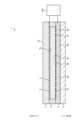
図1は、実施形態1に係る圧力センサの断面構造を表す断面図である。図2は、実施形態1に係るアレイ層を導電層から視た平面図である。図3は、実施形態1に係るアレイ基板に設けられた回路構成を説明するための回路図である。図4は、実施形態1に係る導電層及び封止部を保護層から視た平面図である。図5は、実施形態1に係る圧力センサの使用状態を示した断面図である。図6は、実施形態1に係る圧力センサの製造工程の一部を示す図である。(Embodiment 1)
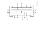
Fig. 1 is a cross-sectional view showing a cross-sectional structure of a pressure sensor according to
図1に示すように、実施形態1に係る圧力センサ1は、接合部材2と、アレイ層3と、導電層4と、封止部5と、対向電極6と、保護層7と、を備える。圧力センサ1のアレイ層3と対向電極6とには、制御部100が接続している。圧力センサ1の各構成は、接合部材2、アレイ層3、導電層4、対向電極6、保護層7の順で積層されている。なお、封止部5は、導電層4と同層である。以下、説明の都合上、圧力センサ1の各構成が積層されている方向を積層方向という。導電層4から視てアレイ層3が配置された方向を第1方向X1とする。導電層4から視て保護層7が配置された方向を第2方向X2という。なお、導電層4はセンサ層と呼ばれることがある。As shown in FIG. 1, the
アレイ層3は、第1方向X1を向く第1面3aと、第2方向X2を向く第2面3bと、を有する。図2に示すように、アレイ層3は、積層方向から視て四角形状の検出領域AA1と、検出領域AA1を囲む四角枠状の非検出領域GG1と、を有する。検出領域AA1は、圧力を検出するための領域である。また、アレイ層3は、タイリングされた複数のアレイ基板30を有する。The
アレイ基板30は、積層方向から視て四角形状の絶縁性基板である。アレイ基板30は、検出領域A1と、非検出領域G1と、を有する(図2の検出領域A1と非検出領域G1との境界線Hを参照)。非検出領域G1は、アレイ基板30の端部に沿って延在し、L字状を成している。検出領域A1には、正方形状の複数のアレイ電極31がマトリックス状に配置されている。The
4つのアレイ基板30は、同一平面上に配置され、かつ各端部が隣接するように並べられている。また、4つのアレイ基板は、それぞれの非検出領域G1が連続して枠状を成すように配置されている。これにより、アレイ層3は、4つの検出領域A1を組み合わせて成る検出領域AA1と、4つの非検出領域G1を組み合わせて成る非検出領域GG1と、を有する。The four
図3に示すように、アレイ基板30は、複数のトランジスタTrと、トランジスタTrのゲート電極に接続するゲート線32aと、トランジスタTrのソース電極と接続する信号検出線33aと、を備える。トランジスタTrのドレイン電極には、各アレイ電極31が接続している。As shown in FIG. 3, the
図2に示すように、非検出領域G1には、複数のゲート線32aに接続するゲートドライバ32と、複数の信号検出線33aに接続するセレクタ33と、が設けられている。ゲートドライバ32は、制御部100の制御信号に基づいて複数のゲート線32aを駆動する回路である。ゲートドライバ32は、複数のゲート線32aを順次又は同時に選択し、選択されたゲート線32aにゲート駆動信号を供給する。セレクタ33は、制御部100の制御信号に基づいて、複数の信号検出線33aのうち、制御部100と接続する信号検出線33aを1つ又は複数選択し、信号検出線33aに入力された信号を制御部100に出力する。As shown in FIG. 2, the non-detection region G1 is provided with a
図1に示すように、接合部材2は、4つのアレイ基板30を接合するためのものである。本実施形態の接合部材2は、積層方向から視てアレイ層3と同形状を成す、一枚(単一)のフィルム部材又はシート部材である。接合部材2は、第1方向X1を向く第1面2aを有する。接合部材2の第1面2aは、アレイ層3の第2面3bに重ねられており、接合部材2がアレイ層3の第2面3bの全面を覆っている。また、接合部材2の第1面2aには、接着剤が塗布されており、接合部材2の第1面2aの全面とアレイ層3の第2面3bの全面とが接着している。これにより、4つのアレイ基板30は接合部材2に固定され、4つのアレイ基板30がそれぞれ分離しないように接合部材2に支持される。さらに、接合部材2は、4つのアレイ基板30の繋ぎ目(アレイ基板30の端部同士が当接する部分)を覆っている。したがって、接合部材2よりも第2方向X2にある液体が4つのアレイ基板30の繋ぎ目に進入することが防止される。なお、図示した例では、4つのアレイ基板30だが、4つ以上のアレイ基板30を1つの接合部材2で接合していてもよい。1, the
導電層4は、積層方向から視てアレイ層3の検出領域AA1(図2参照)と同形状に形成されている。つまり、導電層4は、単一部材から成り、複数のアレイ基板30のそれぞれに跨って積層されている。これにより、アレイ層3の検出領域AA1の全領域において圧力を検出することができる。導電層4は、例えば、絶縁性が高いゴム材料を母材とし、その母材内に導電性の微粒子を分散して成る感圧導電性エマストラーを原材料としている。また、母材の内部に配置された導電性の微粒子は互いに離隔している。よって、導電層4は、通常時(変形していない場合)、非常に高い抵抗値を示し、厚み方向にも面方向にも絶縁性を有している。一方で、導電層4は、押圧されて押圧された箇所の母材が積層方向に圧縮すると、変形個所の母材に含まれる導電性の微粒子同士が互いに接触し、積層方向(厚み方向)に導電性を有する。よって、実施形態1に係る導電層4は、厚み方向からの加圧により抵抗値が変化する感圧材料により形成されている。なお、導電層4は、厚み方向からの加圧により抵抗値が変化する材料であればよく、感圧導電性エマストラーに限定されない。The
導電層4は、アレイ層3に接着されている。例えば、両面接着テープにより導電層4をアレイ層3に接着する場合、両面接着テープは、厚み方向(積層方向)に導電性を有し、面方向に絶縁性を有する、異方性導電材料により製造されている。より詳細に説明すると、両面接着テープは、絶縁性の樹脂又はゴムを母材とし、その母材の内部に導電性の微粒子が分散している。また、導電性の微粒子は、導電層4とアレイ電極31の両者に接触し、かつ、母材の内部の他の微粒子と接触しないように、母材の内部に配置されている。なお、両面接着テープは一例であり、導電層4の接着は、両面接着テープでなく、溶融した樹脂を用いたり、導電層4自体に粘着性を持たせたりしてもよい。樹脂を用いる場合には、導電性の微粒子を分散した光硬化性樹脂や熱硬化性樹脂などが挙げられる。The
図4に示すように、封止部5は、絶縁性を有する樹脂を硬化させて成る。封止部5は、導電層4の外周側を周方向に連続して囲み、四角枠状を成している。封止部5は、積層方向から視て非検出領域GG1と重なっている。図1に示すように、封止部5は、第1方向X1に配置される保護層7と、第2方向に配置されるアレイ層3と、の両者に接触(当接)した状態で介在している。よって、圧力センサ1の側方にある液体が、封止部5と保護層7との間や、封止部5とアレイ層3との間を通過して、導電層4の方に進入しないようになっている。As shown in FIG. 4, the sealing
保護層7は、積層方向から視てアレイ層3と同形状に形成されたフィルム部材又はシート部材である。保護層7の第1面7aは、指やペンなどで押圧される面となっている。保護層7の第2面7bには、対向電極6が成膜されている。保護層7は、絶縁性が高く、かつ剛性が低いゴム又は樹脂により製造されている。よって、保護層7は、第1面7aが押圧された場合、変形するようになっている(図5参照)。The
対向電極6は、保護層7の第2面7bにパターン加工された電極である。対向電極6は、積層方向から視て導電層4と同形状を成すベタ電極である。対向電極6は、導電層4に接着している。なお、例えば両面接着テープで接着する場合は、厚み方向(積層方向)に導電性を有し、面方向に絶縁性を有する、異方性導電材料により製造されている。The
制御部100は、圧力の検出時、対向電極6に基準電圧を印加している。また、制御部100は、図示した例では、4つのアレイ基板30のそれぞれのゲートドライバ32及びセレクタ33に制御信号を送信している。そして、信号検出線33a及びセレクタ33と介して受信した検出信号から導電層4のうち押圧により変形した箇所(座標)と、その押圧力(圧力)と、を測定する。When detecting pressure, the
次に圧力センサ1の動作例を説明する。保護層7の第1面7aが押圧されていない場合、導電層4の厚みが小さくなっていない。よって、導電層4は、厚み方向に絶縁性を有し、対向電極6から導電層4に電流(信号)が流れない。Next, an example of the operation of the
図5に示すように、指により保護層7の第1面7aが第2方向X2に押圧されると、導電層4、対向電極6、及び保護層7が第1方向X1に窪む。これにより、導電層4のうち第1方向X1に窪んだ変形部分の抵抗値が低くなる。よって、対向電極6から導電層4の変形部分に電流が流れる(図5の矢印Aを参照)。そして、制御部100は、アレイ電極31に信号(電流)が入力されたことを検出し、その押圧された箇所(座標)と圧力値を算出することができる。As shown in FIG. 5, when the
また、実施形態1の圧力センサ1によれば、検出領域AA1の中央部(図2の破線Lで囲まれる範囲)を指で押圧した場合、アレイ基板30の検出領域A1と重なっており、押圧された個所の圧力を検出できる。つまり、タイリングされたアレイ基板30の端部が隣接する部分であっても、圧力を検出できる。In addition, according to the
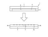
次に圧力センサ1の製造方法を説明する。最初に、接合部材2の第1面2aに4つのアレイ基板30を接着する。次に、対向電極6が印刷された保護層7に導電層4を接着する。次に、導電層4の周囲に樹脂を塗布し硬化させて封止部5を形成する。次に、図6に示すように、導電層4及び封止部5と、アレイ層3と、を接着する。Next, a method for manufacturing the
以上、実施形態1に係る圧力センサ1によれば、検出領域AA1と封止部5とが積層方向に重なっていないため、圧力を検出できる領域が拡大する。また、複数のアレイ基板30をタイリングしているものの、接合部材2がアレイ基板30の繋ぎ目を封止している。また、封止部5が導電層4の外周側を封止している。よって、導電層4の方に液体が進入することが防止される。As described above, according to the
以上、実施形態1に係る圧力センサ1について説明したが、本開示の圧力センサは上記したものに限定されない。例えば、本開示の圧力センサは、異なる製造方法により製造されもよい。以下、他の実施形態について説明するが、実施形態1に係る圧力センサ1との相違点に絞って説明する。The above describes the
(実施形態2)
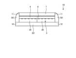
図7は、実施形態2に係る圧力センサの製造工程の一部を示す図である。図7に示すように、実施形態2に係る圧力センサ1Aは、実施形態1に係る圧力センサ1と製造方法が異なる。詳細に説明すると、実施形態2に係る圧力センサ1Aは、最初に、接合部材2の第1面2aに4つのアレイ基板30を接着し、アレイ層3を製造する。次に、アレイ層3の検出領域AA1(図2参照)に、両面接着シートにより導電層4を接着する。次に、アレイ層3の非検出領域GG1(図2参照)に、樹脂を塗布し硬化させて封止部5を形成する。次に、導電層4と封止部5に対し、対向電極6が印刷された保護層7を貼り合わせる。これにより、保護層7と封止部5とが接着し、対向電極6と導電層4とが導通可能に接着する。このような圧力センサ1Aであっても、実施形態1に係る圧力センサ1と同等の効果を奏する。(Embodiment 2)
FIG. 7 is a diagram showing a part of the manufacturing process of the pressure sensor according to the second embodiment. As shown in FIG. 7, the pressure sensor 1A according to the second embodiment is manufactured in a different manner from the
(実施形態3)
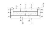
図8は、実施形態3に係る圧力センサの製造工程の一部を示す図である。図8に示すように、実施形態3の圧力センサ1Bは、導電層4が複数の小片導電層40から構成される点で実施形態1に係る圧力センサ1と相違する。つまり、実施形態3の導電層4は、同一平面上(アレイ層3の第1面3a上)に配置され、端部が隣接するように並べられた複数の小片導電層40を備える。そして、封止部5は、複数の小片導電層40から成る導電層4の外周側を囲っている。つまり、導電層4の外周を除き、隣接する小片導電層40の繋ぎ目には、封止部5がない。なお、小片導電層40を用いる場合、アレイ基板30のそれぞれに小片導電層40を接着させて導電層4を製造する。そして、その後、対向電極6が印刷された保護層7を貼り合わせてもよい。若しくは、特に図示しないが、保護層7に印刷された対向電極6に小片導電層40を接着してから、アレイ層3と接着させてもよい。(Embodiment 3)
FIG. 8 is a diagram showing a part of the manufacturing process of the pressure sensor according to the third embodiment. As shown in FIG. 8, the
(実施形態4)
図9は、実施形態4に係る圧力センサの製造工程の一部を示す図である。実施形態4に係る圧力センサ1Cは、封止部5の樹脂が硬化する前に、樹脂を保護層7に接触させる点で実施形態1に係る圧力センサと相違する。具体的に、接合部材2に接着されたアレイ層3の非検出領域GG1(図2参照)に、樹脂を塗布する。そして、樹脂が硬化する前に、導電層4及び保護層7をアレイ層3及び樹脂に重ね合わせ、樹脂を保護層7の縁部に接触させる。なお、アレイ層3の検出領域AA1と導電層4は図示しない両面テープにより接着させる。次に、樹脂を硬化させる。これによれば、封止部5は、アレイ層3の非検出領域GG1と保護層7の両方に固着し、封止性が高い。なお、封止部5を構成する樹脂は、保護層7の縁部のように、最初に塗布し、硬化する前にアレイ層3に接触するようにしてもよい。(Embodiment 4)
FIG. 9 is a diagram showing a part of the manufacturing process of the pressure sensor according to the fourth embodiment. The
上記した実施形態1から実施形態4に係る圧力センサ1、1A、1B、1Cの封止部5は、アレイ層3と保護層7との間に挟まれるように配置されているが、本開示の圧力センサはこれに限定されない。以下、詳細に説明する。The sealing
(実施形態5)
図10は、実施形態5に係る圧力センサの断面構造を示す断面図である。実施形態5の圧力センサ1Dに関し、図10に示すように、アレイ層3と導電層4と保護層7とが積層方向から視て同一形状となっている。よって、圧力センサ1Dは、アレイ層3の側面と、導電層4の側面と、保護層7の側面と、が連続して成る外周面11を有する。また、実施形態5の接合部材2Dは、積層方向から視て、外周面11(アレイ層3と導電層4と保護層7)よりも外側に突出している。封止部5Dは、樹脂を硬化して成る。封止部5Dは、外周面11と、接合部材2Dの端部10と、に跨って固着している。これによれば、外周面11を封止部5Dが覆っているため、圧力センサ1Dの側方からアレイ層3と導電層4と間や導電層4と対向電極6との間に、液体が進入することを防止できる。(Embodiment 5)
FIG. 10 is a cross-sectional view showing the cross-sectional structure of the pressure sensor according to the fifth embodiment. As shown in FIG. 10, the
(実施形態6)
図11は、実施形態6に係る圧力センサの断面構造を示す断面図である。図11に示すように、実施形態6に係る圧力センサ1Eの封止部5Eは、接合部材2Dの端部10と、外周面11と、保護層7の第1面7aの端と、に跨って固着している。これによれば、封止部5Eは、実施形態5の封止部5Dよりも固着面積が大きくなり、剥がれ難い。(Embodiment 6)
Fig. 11 is a cross-sectional view showing the cross-sectional structure of the pressure sensor according to
(実施形態7)
図12は、実施形態7に圧力センサの断面構造を示す断面図である。実施形態7に係る圧力センサ1Fに関し、図12に示すように、接合部材2とアレイ層3と導電層4とが積層方向から視て同一形状となっている。圧力センサ1Fは、接合部材2の側面と、アレイ層3の側面と、導電層4の側面と、が連続して成る外周面14を有する。保護層7Fは、積層方向から視て、外周面14(接合部材2とアレイ層3と導電層4)よりも外側に突出している。封止部5Fは、外周面14と、保護層7の端部13と、に跨って固着している。よって、外周面14を封止部5Fが覆っているため、圧力センサ1Fの側方からアレイ層3と導電層4と間や導電層4と対向電極6との間に、液体が進入し難い。(Embodiment 7)
12 is a cross-sectional view showing the cross-sectional structure of the pressure sensor according to the seventh embodiment. As shown in FIG. 12, the
(実施形態8)
図13は、実施形態8に係る圧力センサの断面構造を示す断面図である。実施形態8に係る圧力センサ1Gに関し、図13に示すように、接合部材2とアレイ層3と導電層4と保護層7とが積層方向から視て同一形状となっている。圧力センサ1Gは、接合部材2の側面と、アレイ層3の側面と、導電層4の側面と、保護層7の側面と、が連続する外周面15を有する。(Embodiment 8)
Fig. 13 is a cross-sectional view showing the cross-sectional structure of the pressure sensor according to embodiment 8. As shown in Fig. 13, in the
封止部5Gは、外周面15に塗布されて硬化している。これによれば、外周面15を封止部5Gが覆っているため、圧力センサ1Gの側方から、アレイ層3と導電層4と間や導電層4と対向電極6との間に、液体が進入することを防止できる。The sealing
上記した封止部は、樹脂を硬化させて成るが、本開示の圧力センサの封止部は、液体の進入を抑制できれば、これに限定さない。次に、シール部材を用いた例を説明する。The sealing portion described above is made by hardening resin, but the sealing portion of the pressure sensor disclosed herein is not limited to this as long as it can prevent the intrusion of liquid. Next, an example using a sealing material will be described.
(実施形態9)
図14は、実施形態9に係る圧力センサの断面構造を示す断面図である。図14に示すように、実施形態9に係る圧力センサ1Hにおいて、接合部材2とアレイ層3と導電層4と保護層7とが積層方向から視て同一形状となっている。圧力センサ1Gは、接合部材2の側面と、アレイ層3の側面と、導電層4の側面と、保護層7の側面とが連続する外周面16を有している。封止部5Hは、フィルム状のシール部材あり、片面にのみ接着層を有している。封止部5Hは、外周面16と、保護層7の第1面7aの端部と、接合部材2の第2面2bの端部と、に跨って接着している。これによれば、圧力センサ1Hの側方から、アレイ層3と導電層4と間や導電層4と対向電極6との間に、液体が進入することを防止できる。(Embodiment 9)
14 is a cross-sectional view showing the cross-sectional structure of the pressure sensor according to the ninth embodiment. As shown in FIG. 14, in the
(実施形態10)
図15は、実施形態10に係る圧力センサの断面構造を示す断面図である。実施形態10に係る圧力センサ1Iは、封止部5Hに代えて封止部5Iを用いている点で、実施形態9に係る圧力センサ1Hと異なる。封止部5Iは、第1シール部材18と、第1シール部材18の第2方向X2に配置される第2シール部材19と、を備える。外周面17のうち積層方向の中央部から第1方向X1を第1シール部材18が被覆し、第2方向X2を第2シール部材19が被覆している。また、第1シール部材18は、保護層の第1面7aの端部に接着している。第2シール部材19は、接合部材2の第2面2bの端部に接着している。また、第1シール部材18の第2方向X2の端部と、第2シール部材19の第1方向X1の端部とが接着している。このような圧力センサ1Iであっても、側方からアレイ層3と導電層4と間や導電層4と対向電極6との間に、液体が進入することを防止できる。(Embodiment 10)
15 is a cross-sectional view showing the cross-sectional structure of the pressure sensor according to the tenth embodiment. The
実施形態1から実施形態10において、導電層4は、押圧による厚みの変化により抵抗値が変化する抵抗変化型のものを挙げて説明したが、本開示の圧力センサの導電層は、積層方向(厚み方向)の厚みの変化により、アレイ電極と対向電極との間に溜まる静電容量が変化する容量変化型のものであってもよい。このような容量変化型の導電層4は、弾性変形が可能であり絶縁性を有するゴム又は高分子化合物により製造される。また、容量変化型の導電層を用いる場合、導電層とアレイ電極との間に介在したり、導電層と対向電極との間に介在したりする両面テープや接着層は、導電性を有していなくてもよい。次に、容量変化型の導電層を用い、アレイ電極31に液体や異物が付着し難い圧力センサについて説明する。In the first to tenth embodiments, the
(実施形態11)
図16は、実施形態11に係る圧力センサの断面構造を示す断面図である。図16に示すように、実施形態11に係る圧力センサ1Jは、アレイ層3の第1面3aに第1封止膜20が設けられている点で、実施形態1に係る圧力センサ1と相違する。第1封止膜20は、アレイ基板30の第1面に形成された4つの小片保護膜21を組み合わせて成る。第1封止膜20(小片保護膜21)は、絶縁材料である、SiOx、SiNx、ポリミド、アクリルなどが挙げられる。本実施形態において、小片保護膜21は、物理蒸着(PVD)法や化学蒸着(CVD)法等によりアレイ基板30と一体に製造される。なお、導電層4は、両面テープや樹脂により第1封止膜20に接着される。(Embodiment 11)
16 is a cross-sectional view showing the cross-sectional structure of the pressure sensor according to the eleventh embodiment. As shown in FIG. 16, the
この実施形態11に係る圧力センサ1Jによれば、各アレイ電極31は第1封止膜20に被覆される。よって、液体や異物がアレイ電極31に付着することが防止できる。よって、第1封止膜20の厚みを薄く形成することができ、圧力センサ1Jの小型化を図れる。また、クロストークやアレイ電極31の腐食を防止することができる。In the
(実施形態12)
図17は、実施形態12に係る圧力センサの断面構造を示す断面図である。図17に示すように、実施形態12に係る圧力センサ1Kは、対向電極6の第2方向X2に第2封止膜22が設けられている点で、実施形態11に係る圧力センサ1Jと相違する。第2封止膜22は、対向電極6の端部6aよりも外側に延びている。第2封止膜22は、対向電極6と、保護層7の第2面7bの端部を覆っている。これによれば、対向電極6の腐食を防止できる。なお、第2封止膜22は、保護層7の第2面7bに、対向電極6を印刷した後、重ねて印刷することで製造される。(Embodiment 12)
17 is a cross-sectional view showing the cross-sectional structure of the pressure sensor according to the twelfth embodiment. As shown in FIG. 17, the
(実施形態13)
図18は、実施形態13に係る圧力センサの断面構造を示す断面図である。図18に示すように、実施形態13に係る圧力センサ1Lは、対向電極6の第1方向X1に第3封止膜23が設けられている点で、実施形態12に係る圧力センサ1Kと相違する。第3封止膜23は、保護層7の第2面7bの全面に形成されている。そして、第3封止膜23と第2封止膜22とで、対向電極6を挟んでいる。また、第3封止膜23と第2封止膜22との外周部は、互いに接触しており、対向電極6の端部6aが露出していない。これによれば、対向電極6はさらに腐食し難くなる。なお、保護層7の第2面7bに、最初に、第3封止膜23を印刷し、次に、対向電極6、第2封止膜22の順で印刷することで製造される。(Embodiment 13)
18 is a cross-sectional view showing the cross-sectional structure of the pressure sensor according to the thirteenth embodiment. As shown in FIG. 18, the
以上、各実施形態について説明したが、接合部材2は、実施形態で説明したフィルム状又はシート状のものに限定されない。例えば、第2方向X2からアレイ基板30同士の繋ぎ目に塗布し、硬化した樹脂部であってもよい。このような樹脂部によれば、各アレイ基板30を接合でき、かつアレイ基板30の間に液体が進入することを防止できる。Although each embodiment has been described above, the
1、1A、1B、1C、1D、1E、1F、1G、1H、1I、1J、1K、1L 圧力センサ
2 接合部材
3 アレイ層
3a 第1面
3b 第2面
4 導電層
5、5D、5E、5F、5G、5H 封止部
6 対向電極
7 保護層
7a 第1面
7b 第2面
11、14、15 外周面
18 第1シール部材
19 第2シール部材
20 第1封止膜
21 小片保護膜
22 第2封止膜
23 第3封止膜
30 アレイ基板
31 アレイ電極
40 小片導電層
A1、AA1 検出領域
G1、GG1 非検出領域 1, 1A, 1B, 1C, 1D, 1E, 1F, 1G, 1H, 1I, 1J, 1K,
6
Claims (7)
Translated fromJapaneseアレイ電極が配置される第1面と、前記第1面と反対側の第2面と、を有する前記アレイ層と、
前記アレイ層の第1面に積層されるセンサ層と、
前記センサ層に積層される保護層と、
前記センサ層と前記保護層との間に介在する対向電極と、
を備え、
前記アレイ層の第2面には、隣接するアレイ基板を接合し、かつ隣接するアレイ基板の繋ぎ目を覆う接合部材が設けられ、
前記センサ層は、複数の前記アレイ基板のそれぞれに跨って積層される単一部材から成り、
前記センサ層の外周側には、枠状の封止部が設けられている
前記センサ層は、前記センサ層の厚みの変化により前記センサ層の抵抗値が変化する抵抗変化型、又は前記センサ層の厚みの変化により前記アレイ電極と対向電極との間の静電容量が変化する容量変化型であり、
前記抵抗変化型は、前記アレイ層の第1面に積層される絶縁層と、前記絶縁層の内部に含まれる複数の導電性の微粒子と、により構成され、
前記容量変化型は、前記アレイ層の第1面に積層される絶縁層で構成される
圧力センサ。 A pressure sensor having an array layer in which a plurality of array substrates are arranged on the same plane and end portions of the array substrates are arranged adjacent to each other,
the array layer having a first surface on which the array electrodes are disposed and a second surface opposite the first surface;
a sensor layer laminated on a first surface of the array layer;
A protective layer laminated onthe sensor layer ;
a counter electrode interposed betweenthe sensor layer and the protective layer;
Equipped with
a bonding member is provided on the second surface of the array layer to bond adjacent array substrates and to cover seams between the adjacent array substrates;
the sensor layer is made of a single member laminated across each of the plurality of array substrates;
A frame-shaped sealing portion is provided on the outer periphery ofthe sensor layer .
the sensor layer is a resistance change type in which a resistance value of the sensor layer changes with a change in thickness of the sensor layer, or a capacitance change type in which an electrostatic capacitance between the array electrode and a counter electrode changes with a change in thickness of the sensor layer,
The resistance change type is composed of an insulating layer laminated on a first surface of the array layer and a plurality of conductive particles contained inside the insulating layer,
The capacitance change type is composed of an insulating layer laminated on the first surface of the array layer.
Pressure sensor.
請求項1に記載の圧力センサ。 The pressure sensoraccording to claim 1 , wherein the joining member is a single protective film that covers the entire second surface of the array layer and is adhered to each of the plurality of array substrates.
請求項1又は請求項2に記載の圧力センサ。 The pressure sensoraccording to claim 1 , wherein the sealing portion is interposed between the array layer and the protection layer.
前記封止部は、前記外周面を覆う
請求項1又は請求項2に記載の圧力センサ。 an outer circumferential surface that is continuous with a side surface of the array layer, a side surface ofthe sensor layer , and a side surface of the protective layer;
The pressure sensor according toclaim 1 , wherein the sealing portion covers the outer circumferential surface.
前記アレイ層と前記センサ層との間には、前記アレイ電極を覆う第1封止膜が設けられている
請求項1から請求項4のいずれか1項に記載の圧力センサ。the sensor layer is ofthe capacitance change type,
The pressure sensor according to claim1 , further comprising a first sealing film provided between the array layer andthe sensor layer to cover the array electrodes.
請求項5に記載の圧力センサ。 The pressure sensor according to claim5 , further comprising a second sealing film disposed betweenthe sensor layer and the protective layer and covering the counter electrode.
請求項6に記載の圧力センサ。 The pressure sensor according to claim6 , further comprising a third sealing film disposed between the counter electrode and the protective layer.
Priority Applications (2)
| Application Number | Priority Date | Filing Date | Title |
|---|---|---|---|
| JP2020155746AJP7576418B2 (en) | 2020-09-16 | 2020-09-16 | Pressure Sensors |
| US17/467,757US11781925B2 (en) | 2020-09-16 | 2021-09-07 | Force sensor including multiple array substrates |
Applications Claiming Priority (1)
| Application Number | Priority Date | Filing Date | Title |
|---|---|---|---|
| JP2020155746AJP7576418B2 (en) | 2020-09-16 | 2020-09-16 | Pressure Sensors |
Publications (2)
| Publication Number | Publication Date |
|---|---|
| JP2022049511A JP2022049511A (en) | 2022-03-29 |
| JP7576418B2true JP7576418B2 (en) | 2024-10-31 |
Family
ID=80626453
Family Applications (1)
| Application Number | Title | Priority Date | Filing Date |
|---|---|---|---|
| JP2020155746AActiveJP7576418B2 (en) | 2020-09-16 | 2020-09-16 | Pressure Sensors |
Country Status (2)
| Country | Link |
|---|---|
| US (1) | US11781925B2 (en) |
| JP (1) | JP7576418B2 (en) |
Families Citing this family (1)
| Publication number | Priority date | Publication date | Assignee | Title |
|---|---|---|---|---|
| US12066347B2 (en)* | 2020-07-28 | 2024-08-20 | Sanctuary Cognitive Systems Corporation | Sensory array structures with two or more different sets of resolution, method of fabrication of and method of operating same |
Citations (6)
| Publication number | Priority date | Publication date | Assignee | Title |
|---|---|---|---|---|
| JP2015215306A (en) | 2014-05-13 | 2015-12-03 | 住友電気工業株式会社 | Pressure sensitive sensor and manufacturing method thereof |
| WO2016027495A1 (en) | 2014-08-22 | 2016-02-25 | 株式会社村田製作所 | Piezoelectric sensor and detection device |
| US20160077649A1 (en) | 2013-05-27 | 2016-03-17 | Murata Manufacturing Co., Ltd. | Display panel with pressure sensor and electronic device with pressing input function |
| US20180300005A1 (en) | 2015-10-05 | 2018-10-18 | Amogreentech Co., Ltd. | Apparatus for sensing touch pressure |
| US20200089367A1 (en) | 2018-09-13 | 2020-03-19 | Sensel, Inc. | Method and apparatus for variable impedence touch sensor array force aware interaction in large surface devices |
| WO2020116445A1 (en) | 2018-12-06 | 2020-06-11 | ソニー株式会社 | Pressure sensor and electronic device |
Family Cites Families (42)
| Publication number | Priority date | Publication date | Assignee | Title |
|---|---|---|---|---|
| DE3634855C1 (en)* | 1986-10-13 | 1988-03-31 | Peter Seitz | Capacitive measuring arrangement for the determination of forces and / or pressures |
| US5942733A (en)* | 1992-06-08 | 1999-08-24 | Synaptics, Inc. | Stylus input capacitive touchpad sensor |
| DE4236133C1 (en)* | 1992-10-26 | 1994-03-10 | Siemens Ag | Sensor arrangement for recording fingerprints and method for their production |
| JPH0765943B2 (en) | 1993-03-24 | 1995-07-19 | イナバゴム株式会社 | Pressure distribution condition measuring device |
| JPH1038720A (en)* | 1996-07-19 | 1998-02-13 | Nippon Telegr & Teleph Corp <Ntt> | Large area pressure distribution sensor |
| DE19839606C1 (en)* | 1998-08-31 | 2000-04-27 | Siemens Ag | Micromechanical component and method for its production |
| JP2004109066A (en)* | 2002-09-20 | 2004-04-08 | Sanyo Electric Co Ltd | Pressure pattern sensor and its operation control method |
| US7080562B2 (en)* | 2003-10-17 | 2006-07-25 | Qortek, Inc. | High-sensitivity pressure conduction sensor for localized pressures and stresses |
| JP4776902B2 (en)* | 2003-11-19 | 2011-09-21 | 株式会社豊田中央研究所 | Mechanical quantity sensor element |
| US6964205B2 (en)* | 2003-12-30 | 2005-11-15 | Tekscan Incorporated | Sensor with plurality of sensor elements arranged with respect to a substrate |
| US7343813B1 (en)* | 2005-02-15 | 2008-03-18 | Harrington Richard H | Multicapacitor sensor array |
| US9018030B2 (en)* | 2008-03-20 | 2015-04-28 | Symbol Technologies, Inc. | Transparent force sensor and method of fabrication |
| US9459734B2 (en)* | 2009-04-06 | 2016-10-04 | Synaptics Incorporated | Input device with deflectable electrode |
| US9383881B2 (en)* | 2009-06-03 | 2016-07-05 | Synaptics Incorporated | Input device and method with pressure-sensitive layer |
| WO2010143528A1 (en)* | 2009-06-11 | 2010-12-16 | 株式会社村田製作所 | Touch screen and touch-type input device |
| JPWO2011039798A1 (en)* | 2009-09-29 | 2013-02-21 | パイオニア株式会社 | MEMS sensor and sensor array including the same |
| JP4896198B2 (en)* | 2009-10-14 | 2012-03-14 | 国立大学法人東北大学 | Tactile sensor system |
| US9281415B2 (en)* | 2010-09-10 | 2016-03-08 | The Board Of Trustees Of The Leland Stanford Junior University | Pressure sensing apparatuses and methods |
| JP2014122947A (en)* | 2012-12-20 | 2014-07-03 | Japan Display Inc | Display device and cover member |
| TWI470197B (en)* | 2012-12-20 | 2015-01-21 | Ind Tech Res Inst | Capacitive shear force sensor and method for fabricating thereof |
| JP6194233B2 (en)* | 2013-01-08 | 2017-09-06 | 株式会社ジャパンディスプレイ | Manufacturing method of display device |
| US10120478B2 (en)* | 2013-10-28 | 2018-11-06 | Apple Inc. | Piezo based force sensing |
| US9367094B2 (en)* | 2013-12-17 | 2016-06-14 | Apple Inc. | Display module and system applications |
| AU2015100011B4 (en)* | 2014-01-13 | 2015-07-16 | Apple Inc. | Temperature compensating transparent force sensor |
| US10126153B2 (en)* | 2014-07-22 | 2018-11-13 | Deere & Company | Particulate matter impact sensor |
| US9690408B1 (en)* | 2014-09-26 | 2017-06-27 | Apple Inc. | Electronic device with an integrated touch sensing and force sensing device |
| WO2016118796A1 (en)* | 2015-01-22 | 2016-07-28 | Interface, Inc. | Floor covering system with sensors |
| JP2017120310A (en)* | 2015-12-28 | 2017-07-06 | 株式会社ジャパンディスプレイ | Display device, adhesive sheet used for display device, and method for manufacturing the display device |
| JP6646451B2 (en)* | 2016-01-14 | 2020-02-14 | 株式会社ジャパンディスプレイ | Cover member and display device having the same |
| US10442091B2 (en)* | 2016-01-29 | 2019-10-15 | Ricoh Company, Ltd. | Pressure-sensitive sensor, gripping device, and robot |
| EP3428595A4 (en)* | 2016-03-11 | 2019-03-20 | Ricoh Company, Ltd. | EMERGENCY STOP PRESSURE SENSOR, SAFETY DEVICE AND SECURITY SYSTEM |
| EP3469323A4 (en)* | 2016-06-08 | 2020-03-18 | The University of British Columbia | Surface sensor arrays using ionically conducting material |
| US11320329B2 (en)* | 2016-09-12 | 2022-05-03 | Sitime Corporation | Frequency-modulating sensor array |
| JP6915902B2 (en)* | 2017-03-08 | 2021-08-04 | 国立大学法人東北大学 | Manufacturing method of pressure-sensitive sensor device and pressure-sensitive sensor device |
| JP6857563B2 (en)* | 2017-07-04 | 2021-04-14 | 株式会社ジャパンディスプレイ | Detection device and display device |
| US11093088B2 (en)* | 2017-08-08 | 2021-08-17 | Cambridge Touch Technologies Ltd. | Device for processing signals from a pressure-sensing touch panel |
| JP6909748B2 (en)* | 2018-03-26 | 2021-07-28 | 住友理工株式会社 | Transducer sheet |
| DE102018221047A1 (en)* | 2018-04-05 | 2019-10-10 | Continental Reifen Deutschland Gmbh | Apparatus for measuring a mechanical force comprising first, second, third, fourth and fifth layers and the uses of the apparatus and tires or engineering rubber articles comprising the apparatus |
| US10729067B2 (en)* | 2018-10-20 | 2020-08-04 | Deere & Company | Biomass impact sensor having a conformal encasement enveloping a pressure sensitive film |
| KR102663292B1 (en)* | 2018-11-23 | 2024-05-02 | 엘지디스플레이 주식회사 | Display apparatus and automotive apparatus |
| US11493392B2 (en)* | 2019-10-03 | 2022-11-08 | Ricoh Company, Ltd. | Sensor sheet, robot hand, and glove |
| US11106309B1 (en)* | 2021-01-07 | 2021-08-31 | Anexa Labs Llc | Electrode touch display |
- 2020
- 2020-09-16JPJP2020155746Apatent/JP7576418B2/enactiveActive
- 2021
- 2021-09-07USUS17/467,757patent/US11781925B2/enactiveActive
Patent Citations (6)
| Publication number | Priority date | Publication date | Assignee | Title |
|---|---|---|---|---|
| US20160077649A1 (en) | 2013-05-27 | 2016-03-17 | Murata Manufacturing Co., Ltd. | Display panel with pressure sensor and electronic device with pressing input function |
| JP2015215306A (en) | 2014-05-13 | 2015-12-03 | 住友電気工業株式会社 | Pressure sensitive sensor and manufacturing method thereof |
| WO2016027495A1 (en) | 2014-08-22 | 2016-02-25 | 株式会社村田製作所 | Piezoelectric sensor and detection device |
| US20180300005A1 (en) | 2015-10-05 | 2018-10-18 | Amogreentech Co., Ltd. | Apparatus for sensing touch pressure |
| US20200089367A1 (en) | 2018-09-13 | 2020-03-19 | Sensel, Inc. | Method and apparatus for variable impedence touch sensor array force aware interaction in large surface devices |
| WO2020116445A1 (en) | 2018-12-06 | 2020-06-11 | ソニー株式会社 | Pressure sensor and electronic device |
Also Published As
| Publication number | Publication date |
|---|---|
| US20220082457A1 (en) | 2022-03-17 |
| JP2022049511A (en) | 2022-03-29 |
| US11781925B2 (en) | 2023-10-10 |
Similar Documents
| Publication | Publication Date | Title |
|---|---|---|
| US10698447B2 (en) | Rollable display device and rollable device | |
| CN102822779B (en) | It is respectively provided with the transparent piezoelectric sheet of the tape frame of transparent piezoelectric sheet, contact type panel and electronic installation | |
| JP5885865B2 (en) | Pressure detection device and information input device | |
| JP7186685B2 (en) | pressure sensor | |
| KR101479380B1 (en) | A laminated structure, a touch display having a laminated structure, and a laminating method thereof | |
| US20170004343A1 (en) | Touch Panel with Fingerprint Identification Function and Method for Fabricating the Same | |
| CN101957513A (en) | The electronic unit of band fender | |
| JP5111071B2 (en) | Piezoelectric sensor | |
| CN103853376A (en) | Display device including touch panel and method of fabricating the same | |
| JP7576418B2 (en) | Pressure Sensors | |
| CN108153440B (en) | Flexible touch display screen and manufacturing method thereof | |
| JP7641002B2 (en) | Pressure-sensitive element | |
| WO2011024903A1 (en) | Pressure detection unit | |
| JP2008209695A (en) | Electrophoretic display device and manufacturing method thereof | |
| CN116499617A (en) | Pressure Sensor | |
| US20250077002A1 (en) | Detection device with thermal protection arrangement | |
| US12287942B2 (en) | Touch-interface arrangement | |
| US20240295449A1 (en) | Force distribution sensor | |
| JP2025140580A (en) | Detection Device | |
| CN222505670U (en) | Load detection device | |
| JP2023108953A (en) | pressure sensor | |
| JP2025140581A (en) | Detection Device | |
| JP2024092236A (en) | Stress sensor and stress detection sheet | |
| CN101069253A (en) | Reinforced foil-type switching element | |
| TWM416138U (en) | Touch input device |
Legal Events
| Date | Code | Title | Description |
|---|---|---|---|
| A621 | Written request for application examination | Free format text:JAPANESE INTERMEDIATE CODE: A621 Effective date:20230816 | |
| A977 | Report on retrieval | Free format text:JAPANESE INTERMEDIATE CODE: A971007 Effective date:20240523 | |
| A131 | Notification of reasons for refusal | Free format text:JAPANESE INTERMEDIATE CODE: A131 Effective date:20240702 | |
| A521 | Request for written amendment filed | Free format text:JAPANESE INTERMEDIATE CODE: A523 Effective date:20240829 | |
| TRDD | Decision of grant or rejection written | ||
| A01 | Written decision to grant a patent or to grant a registration (utility model) | Free format text:JAPANESE INTERMEDIATE CODE: A01 Effective date:20241001 | |
| A61 | First payment of annual fees (during grant procedure) | Free format text:JAPANESE INTERMEDIATE CODE: A61 Effective date:20241021 | |
| R150 | Certificate of patent or registration of utility model | Ref document number:7576418 Country of ref document:JP Free format text:JAPANESE INTERMEDIATE CODE: R150 |