JP7574860B2 - Image pickup element and image pickup device - Google Patents
Image pickup element and image pickup deviceDownload PDFInfo
- Publication number
- JP7574860B2 JP7574860B2JP2022565016AJP2022565016AJP7574860B2JP 7574860 B2JP7574860 B2JP 7574860B2JP 2022565016 AJP2022565016 AJP 2022565016AJP 2022565016 AJP2022565016 AJP 2022565016AJP 7574860 B2JP7574860 B2JP 7574860B2
- Authority
- JP
- Japan
- Prior art keywords
- light
- pixel
- wavelength
- pixels
- structures
- Prior art date
- Legal status (The legal status is an assumption and is not a legal conclusion. Google has not performed a legal analysis and makes no representation as to the accuracy of the status listed.)
- Active
Links
Images


Classifications
- H—ELECTRICITY
- H10—SEMICONDUCTOR DEVICES; ELECTRIC SOLID-STATE DEVICES NOT OTHERWISE PROVIDED FOR
- H10F—INORGANIC SEMICONDUCTOR DEVICES SENSITIVE TO INFRARED RADIATION, LIGHT, ELECTROMAGNETIC RADIATION OF SHORTER WAVELENGTH OR CORPUSCULAR RADIATION
- H10F39/00—Integrated devices, or assemblies of multiple devices, comprising at least one element covered by group H10F30/00, e.g. radiation detectors comprising photodiode arrays
- H10F39/80—Constructional details of image sensors
- H10F39/805—Coatings
- H10F39/8053—Colour filters
- H—ELECTRICITY
- H10—SEMICONDUCTOR DEVICES; ELECTRIC SOLID-STATE DEVICES NOT OTHERWISE PROVIDED FOR
- H10F—INORGANIC SEMICONDUCTOR DEVICES SENSITIVE TO INFRARED RADIATION, LIGHT, ELECTROMAGNETIC RADIATION OF SHORTER WAVELENGTH OR CORPUSCULAR RADIATION
- H10F39/00—Integrated devices, or assemblies of multiple devices, comprising at least one element covered by group H10F30/00, e.g. radiation detectors comprising photodiode arrays
- H10F39/80—Constructional details of image sensors
- H10F39/806—Optical elements or arrangements associated with the image sensors
- G—PHYSICS
- G02—OPTICS
- G02B—OPTICAL ELEMENTS, SYSTEMS OR APPARATUS
- G02B1/00—Optical elements characterised by the material of which they are made; Optical coatings for optical elements
- G02B1/002—Optical elements characterised by the material of which they are made; Optical coatings for optical elements made of materials engineered to provide properties not available in nature, e.g. metamaterials
- G—PHYSICS
- G02—OPTICS
- G02B—OPTICAL ELEMENTS, SYSTEMS OR APPARATUS
- G02B5/00—Optical elements other than lenses
- G02B5/20—Filters
- G—PHYSICS
- G02—OPTICS
- G02B—OPTICAL ELEMENTS, SYSTEMS OR APPARATUS
- G02B5/00—Optical elements other than lenses
- G02B5/20—Filters
- G02B5/201—Filters in the form of arrays
- G—PHYSICS
- G02—OPTICS
- G02B—OPTICAL ELEMENTS, SYSTEMS OR APPARATUS
- G02B5/00—Optical elements other than lenses
- G02B5/20—Filters
- G02B5/208—Filters for use with infrared or ultraviolet radiation, e.g. for separating visible light from infrared and/or ultraviolet radiation
- H—ELECTRICITY
- H04—ELECTRIC COMMUNICATION TECHNIQUE
- H04N—PICTORIAL COMMUNICATION, e.g. TELEVISION
- H04N23/00—Cameras or camera modules comprising electronic image sensors; Control thereof
- H04N23/10—Cameras or camera modules comprising electronic image sensors; Control thereof for generating image signals from different wavelengths
- H04N23/11—Cameras or camera modules comprising electronic image sensors; Control thereof for generating image signals from different wavelengths for generating image signals from visible and infrared light wavelengths
- H—ELECTRICITY
- H10—SEMICONDUCTOR DEVICES; ELECTRIC SOLID-STATE DEVICES NOT OTHERWISE PROVIDED FOR
- H10F—INORGANIC SEMICONDUCTOR DEVICES SENSITIVE TO INFRARED RADIATION, LIGHT, ELECTROMAGNETIC RADIATION OF SHORTER WAVELENGTH OR CORPUSCULAR RADIATION
- H10F39/00—Integrated devices, or assemblies of multiple devices, comprising at least one element covered by group H10F30/00, e.g. radiation detectors comprising photodiode arrays
- H10F39/80—Constructional details of image sensors
- H10F39/802—Geometry or disposition of elements in pixels, e.g. address-lines or gate electrodes
- H—ELECTRICITY
- H10—SEMICONDUCTOR DEVICES; ELECTRIC SOLID-STATE DEVICES NOT OTHERWISE PROVIDED FOR
- H10F—INORGANIC SEMICONDUCTOR DEVICES SENSITIVE TO INFRARED RADIATION, LIGHT, ELECTROMAGNETIC RADIATION OF SHORTER WAVELENGTH OR CORPUSCULAR RADIATION
- H10F39/00—Integrated devices, or assemblies of multiple devices, comprising at least one element covered by group H10F30/00, e.g. radiation detectors comprising photodiode arrays
- H10F39/80—Constructional details of image sensors
- H10F39/805—Coatings
- G—PHYSICS
- G02—OPTICS
- G02B—OPTICAL ELEMENTS, SYSTEMS OR APPARATUS
- G02B1/00—Optical elements characterised by the material of which they are made; Optical coatings for optical elements
- G02B1/02—Optical elements characterised by the material of which they are made; Optical coatings for optical elements made of crystals, e.g. rock-salt, semi-conductors
- H—ELECTRICITY
- H10—SEMICONDUCTOR DEVICES; ELECTRIC SOLID-STATE DEVICES NOT OTHERWISE PROVIDED FOR
- H10F—INORGANIC SEMICONDUCTOR DEVICES SENSITIVE TO INFRARED RADIATION, LIGHT, ELECTROMAGNETIC RADIATION OF SHORTER WAVELENGTH OR CORPUSCULAR RADIATION
- H10F39/00—Integrated devices, or assemblies of multiple devices, comprising at least one element covered by group H10F30/00, e.g. radiation detectors comprising photodiode arrays
- H10F39/10—Integrated devices
- H10F39/12—Image sensors
- H10F39/18—Complementary metal-oxide-semiconductor [CMOS] image sensors; Photodiode array image sensors
- H10F39/182—Colour image sensors
- H—ELECTRICITY
- H10—SEMICONDUCTOR DEVICES; ELECTRIC SOLID-STATE DEVICES NOT OTHERWISE PROVIDED FOR
- H10F—INORGANIC SEMICONDUCTOR DEVICES SENSITIVE TO INFRARED RADIATION, LIGHT, ELECTROMAGNETIC RADIATION OF SHORTER WAVELENGTH OR CORPUSCULAR RADIATION
- H10F39/00—Integrated devices, or assemblies of multiple devices, comprising at least one element covered by group H10F30/00, e.g. radiation detectors comprising photodiode arrays
- H10F39/10—Integrated devices
- H10F39/12—Image sensors
- H10F39/199—Back-illuminated image sensors
- H—ELECTRICITY
- H10—SEMICONDUCTOR DEVICES; ELECTRIC SOLID-STATE DEVICES NOT OTHERWISE PROVIDED FOR
- H10F—INORGANIC SEMICONDUCTOR DEVICES SENSITIVE TO INFRARED RADIATION, LIGHT, ELECTROMAGNETIC RADIATION OF SHORTER WAVELENGTH OR CORPUSCULAR RADIATION
- H10F39/00—Integrated devices, or assemblies of multiple devices, comprising at least one element covered by group H10F30/00, e.g. radiation detectors comprising photodiode arrays
- H10F39/80—Constructional details of image sensors
- H10F39/802—Geometry or disposition of elements in pixels, e.g. address-lines or gate electrodes
- H10F39/8023—Disposition of the elements in pixels, e.g. smaller elements in the centre of the imager compared to larger elements at the periphery
Landscapes
- Physics & Mathematics (AREA)
- General Physics & Mathematics (AREA)
- Optics & Photonics (AREA)
- Health & Medical Sciences (AREA)
- Toxicology (AREA)
- Engineering & Computer Science (AREA)
- Multimedia (AREA)
- Signal Processing (AREA)
- Solid State Image Pick-Up Elements (AREA)
- Optical Elements Other Than Lenses (AREA)
- Optical Filters (AREA)
- Color Television Image Signal Generators (AREA)
Description
Translated fromJapanese本発明は、撮像素子及び撮像装置に関する。 The present invention relates toan imaging element and an imaging device.
一般的な撮像装置は、レンズ光学系と、CCD:Charge Coupled Device)センサやCMOS(Complementary Metal Oxide Semiconductor)センサなどの2次元撮像素子とを用いて、撮像対象からの光の強度情報と色情報からなる2次元画像を取得する。A typical imaging device uses a lens optical system and a two-dimensional imaging element such as a CCD (Charge Coupled Device) sensor or a CMOS (Complementary Metal Oxide Semiconductor) sensor to obtain a two-dimensional image consisting of light intensity information and color information from the subject.
近年、可視光(色情報)に加えて近赤外(NIR:Near-Infrared)光の画像を同時撮像への要求が高まっている。近赤外線撮像装置は、夜間撮影が可能となるため、車載カメラや監視カメラなどの用途で注目されている。In recent years, there has been an increasing demand for simultaneous imaging of near-infrared (NIR) light in addition to visible light (color information). Near-infrared imaging devices are attracting attention for use in vehicle-mounted cameras, surveillance cameras, and other applications because they enable nighttime imaging.
そこで、可視光の色情報及び近赤外線画像の双方を撮影する撮像素子として、色情報およびNIR情報の取得のため、各画素上に、R(赤)、G(緑)、B(青)にNIRを加えた4種類のカラーフィルタを集積する構成が提案されている。Therefore, as an imaging element that captures both visible light color information and near-infrared images, a configuration has been proposed in which four types of color filters - R (red), G (green), B (blue) plus NIR - are integrated on each pixel to obtain color information and NIR information.
しかしながら、従来の撮像素子では、カラーフィルタによる透過波長帯域外の光の吸収により、フィルタ透過後の総受光量が減少し、感度に制限があるという問題があった。そして、一般的な色フィルタはNIR波長領域の光を一部透過するため、従来の撮像素子では、カラー画像を生成するために、R,G,B画素値からNIR画素値を減ずる等の色の校正が必要であった。However, conventional image sensors have a problem in that the total amount of light received after passing through the filter is reduced due to the absorption of light outside the transmission wavelength band by the color filter, limiting the sensitivity. Furthermore, because general color filters transmit some light in the NIR wavelength range, conventional image sensors require color calibration, such as subtracting the NIR pixel value from the R, G, and B pixel values, to generate a color image.
本発明は、上記に鑑みてなされたものであって、光吸収を起こすことなく、入射光の可視光と近赤外光との受光感度を向上することができる撮像素子及び撮像装置を提供することを目的とする。 The present invention has been made in consideration of the above, and aims to provide animaging element and an imaging device that can improve the light receiving sensitivity of incident visible light and near-infrared light without causing light absorption.
上述した課題を解決し、目的を達成するために、本発明に係る撮像素子は、各々が光電変換素子を含む複数の画素と、複数の画素を覆う透明層と、透明層上または透明層内において透明層の面方向に配置された複数の構造体と、を備える素子であって、複数の構造体は、入射した光のうち、波長が近赤外光領域である第1の光を複数の画素のうちの第1の画素に集光し、波長が近赤外領域外の領域である第2の色の光を第2の画素に集光するように配置され、複数の構造体は、1つの画素と対向する領域の外側に入射した光のうちの当該1つの画素に対応する波長の光も当該1つの画素に集光するように配置され、入射した光を集光するためのマイクロレンズを含まずに構成されることを特徴とする。 In order to solve the above-mentioned problems and achieve the object,the imaging element of the present invention is an element comprising a plurality of pixels each including a photoelectric conversion element, a transparent layer covering the plurality of pixels, and a plurality of structures arranged in the surface direction of the transparent layer on or within the transparent layer, wherein the plurality of structures are arranged to focus a first light of incident light having a wavelength in the near-infrared light region onto a first pixel of the plurality of pixels and to focus light of a second color having a wavelength outside the near-infrared region onto a second pixel, the plurality of structures are arranged to also focus light of a wavelength corresponding to one pixel among light incident outside a region facing a single pixel onto the single pixel, and are characterized in that the imaging element is configured without including a microlens for focusing the incident light.
また、本発明に係る光学素子は、各々が光電変換素子を含む複数の画素を覆うための透明層と、透明層上または透明層内において透明層の面方向に配置された複数の構造体と、を備え、複数の構造体は、入射した光のうち、近赤外光領域である第1の光を出力し、入射した光のうち、波長が近赤外領域外の領域である第2の色の光を出力することを特徴とする。The optical element according to the present invention further comprises a transparent layer for covering a plurality of pixels, each of which includes a photoelectric conversion element, and a plurality of structures arranged in the plane direction of the transparent layer on or within the transparent layer, the plurality of structures being characterized in that they output a first color of incident light that is in the near-infrared light region, and output a second color of incident light that has a wavelength in a region outside the near-infrared region.
また、本発明に係る撮像装置は、上記の撮像素子と、撮像素子から得られた電気信号に基づいて画像信号を生成する信号処理部と、を備えることを特徴とする。The imaging device according to the present invention is characterized by comprising the above-mentioned imaging element and a signal processing unit that generates an image signal based on the electrical signal obtained from the imaging element.
本発明によれば、光吸収を起こすことなく、入射光の可視光との受光感度を向上することができる。According to the present invention, it is possible to improve the light receiving sensitivity of incident visible light without causing light absorption.
以下、本発明を実施するための最良の形態を図面とともに詳細に説明する。なお、以下の説明において、各図は本発明の内容を理解でき得る程度に形状、大きさ、及び位置関係を概略的に示してあるに過ぎず、したがって、本発明は各図で例示された形状、大きさ、及び位置関係のみに限定されるものではない。また、図面の記載において、同一部分には同一の符号を付して示している。The best mode for carrying out the present invention will be described in detail below with reference to the drawings. Note that in the following description, each figure merely shows a schematic representation of the shape, size, and positional relationship to the extent that the contents of the present invention can be understood, and therefore the present invention is not limited to only the shape, size, and positional relationship exemplified in each figure. Also, in the description of the drawings, the same parts are denoted by the same reference numerals.
[実施の形態1]
[撮像装置]
まず、本発明の実施の形態1に係る撮像装置について説明する。図1は、実施の形態1に係る撮像装置の概略構成を示した側面図である。[First embodiment]
[Imaging device]
First, an image pickup apparatus according to a first embodiment of the present invention will be described below. Fig. 1 is a side view showing a schematic configuration of the image pickup apparatus according to the first embodiment.
図1に示すように、実施の形態1に係る撮像装置10は、レンズ光学系11、撮像素子12及び信号処理部13を有する。レンズ光学系11は、CCDやCMOS等の光電変換素子を有する。信号処理部13は、撮像素子12から出力される光電変換信号を処理して画像信号を生成する。1, the imaging device 10 according to the first embodiment has a lens
自然光や照明光等の光が物体1に照射され、物体1により透過/反射/散乱した光、または、物体1から発する光は、レンズ光学系11により撮像素子12上に光学像を形成する。一般に、レンズ光学系11は、様々な光学収差を補正するため、光軸に沿って並んだ複数のレンズからなるレンズ群により構成されるが、図1では図面を簡略化して単一のレンズとして示している。信号処理部13は、生成した画像信号を外部に送出する画像信号出力を有する。Natural light, illumination light, or other light is irradiated onto
なお、撮像装置10は、赤外光カットの光学フィルタ、電子シャッタ、ビューファインダ、電源(電池)、フラッシュライトなどの公知の構成要素を備え得るが、それらの説明は、本発明の理解に特に必要でないため省略する。また、以上の構成はあくまでも一例であり、実施の形態1では、レンズ光学系11、撮像素子12、信号処理部13を除く構成要素として、公知の要素を適切に組み合わせて用いることができる。The imaging device 10 may include known components such as an infrared light blocking optical filter, an electronic shutter, a viewfinder, a power source (battery), and a flashlight, but a description of these components is omitted as they are not particularly necessary for understanding the present invention. Also, the above configuration is merely an example, and in the first embodiment, known elements can be used in appropriate combination as components other than the lens
[撮像素子]
続いて、実施の形態1に係る撮像素子12の概略を説明する。本実施の形態1に係る撮像素子12は、光電変換素子を含む画素が2次元アレイ状に複数配列された画素アレイと、波長分離機能と各画素への集光機能とを有する複数の微細な構造体が全面に配列された光学素子アレイ(光学素子)とを有する。なお、以降では、撮像素子12の一部を、撮像素子100として説明する。[Image sensor]
Next, an overview of the
図2は、撮像素子を平面視したときに画素アレイの画素配置を模式的に示す図である。図3は、図2のa-a´線に沿って側面視したときの撮像素子100の断面の一例を示す図である。図4は、図2のb-b´線に沿って側面視したときの撮像素子100の断面の一例を示す図である。なお、図3及び図4において、矢印は、撮像素子100に入射する光を模式的に示す。図5は、図2に示す光学素子アレイにおける構造体の平面視したときの形状及び配置の一例を示す平面図である。図において、xyz座標系が示される。xy平面方向は、後述する画素アレイ110、透明層150等の面方向に相当する。以下、特に説明がある場合を除き、「平面視」は、z軸方向に(例えばz軸負方向に)視ることを指し示す。「側面視」は、x軸方向またはy軸方向(例えばy軸負方向)に見ることを指し示す。2 is a diagram showing a schematic diagram of the pixel arrangement of the pixel array when the imaging element is viewed in a plan view. FIG. 3 is a diagram showing an example of a cross section of the
図3及び図4に示すように、撮像素子100は、画素アレイ110と、画素アレイ110と対向して配置された光学素子アレイ120とを有する。画素アレイ110及び光学素子アレイ120は、z軸正方向にこの順に設けられる。3 and 4, the
図2~図4に示すように、光学素子アレイ120は、レンズ光学系11からの光が入射する側に配置されている。光学素子アレイ120は、画素アレイ110上に形成された透明層150の上面に形成される。なお、透明層150は、SiO2(屈折率n=1.45)等の材料からなる低屈折率の透明層である。 2 to 4, the
画素アレイ110は、配線層180と、xy平面方向に配値された複数画素130とを有する。各画素130は、各々が光電変換素子を含んで構成される。光電変換素子の例は、フォトダイオード(PD:Photo Diode)である。各画素は、赤色(R)、緑色(G)、青色(B)及び近赤外(NIR)に対応する。赤色の光の波長帯域の例は、波長をλ0とすると、600nm<λ0≦800nmである。緑色の光の波長帯域の例は、500nm<λ0≦600nmである。青色の光の波長帯域の例は、λ0≦500nm未満である。近赤外光の波長帯域の例は、800~1000nmである。各画素を区別できるように、画素R、画素G、画素B及び画素NIRと称し図示する。これら4つの画素R、画素G、画素B及び画素NIRは、図2に示すように、ベイヤー配列され、一つの画素ユニットU1を構成する。 The
入射した光は、z軸負方向に沿って進み、光学素子アレイ120を介して画素アレイ110に到達する。光学素子アレイ120は、入射した光のうちの赤色の光を画素Rに集光し、緑色の光を画素Gに集光し、青色の光を画素Bに集光し、近赤外光を画素NIRに集光する。これらの画素R、画素G、画素B及び画素NIRで発生した電荷は、図示しないトランジスタ等によって、画素信号の基礎となる電気信号に変換され、配線層180を介して撮像素子100の外部に出力される。図3及び図4では、配線層180に含まれる配線のいくつかが図示される。The incident light travels along the negative z-axis direction and reaches the
光学素子アレイ120は、画素アレイ110を覆うように設けられる。光学素子アレイ120の例は、メタサーフェスである。メタサーフェスは、光の波長以下の幅を有する複数の微細構造体(構造体160に相当)を含んで構成される。メタサーフェスは、2次元構造を有してもよいし、3次元構造を有してもよい。光学素子アレイ120は、この構造体160のパラメータを変えるだけで、光の特性(波長、偏波、入射角)に応じて、位相と光強度を制御することができる。3次元構造の場合、2次元構造よりも設計自由度が向上する。The
光学素子アレイ120は、波長分離機能及びレンズ機能の2つの機能を有する。波長分離機能は、入射した光を各波長帯域の光に分離する機能である。レンズ機能は、各波長の光を、対応する画素に集光する機能である。この例では、光学素子アレイ120の波長分離機能により、入射した光が赤色の光、緑色の光、青色の光及びNIR光に分離される。レンズ機能により、赤色の光が画素Rに集光され、緑色の光が画素Gに集光され、青色の光が画素Bに集光され、NIR光が画素NIRに集光される。The
光学素子アレイ120は、透明層150と、複数の構造体160とを含む。透明層150は、画素アレイ110を覆うように、画素アレイ110上に設けられる。透明層150は、構造体160の屈折率よりも低い屈折率を有する。透明層150の材料の例は、SiO2等である。透明層150は空隙であってもよく、その場合、透明層150の屈折率は、空気の屈折率に等しくてよい。透明層150の材料は単一であってもよいし、複数の材料が層状になったものでもよい。 The
複数の構造体160は、透明層150上または透明層150内において、透明層150の面方向(xy平面方向)に、例えば周期的に(周期構造を有して)、配置される。この例では、構造体160は、透明層150を挟んで画素アレイ110とは反対側(z軸正方向側)において、透明層150上に設けられる。複数の構造体160は、設計を容易にする等のために等間隔配置されてもよいし、不等間隔配置されてもよい。各構造体160は、入射光の波長と同程度またはそれよりも小さい寸法を有するナノオーダーサイズの微細構造体である。複数の構造体160は、側面視したときに、同じ高さを有する。The
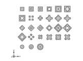
図5には、図2の画素ユニットU1に対応する領域の複数の構造体160の平面視したときの形状及び配置の例が模式的に示される。構造体160は、平面視したときに、例えば、正方形形状、十字形状、円形形状を有する。正方形形状、十字形状、円形形状の構造体160の各々は、基本形状が同じで異なる寸法(長さ、幅等)を有する。構造体160の平面視したときの形状は、4回回転対称形状であってよい。そのような形状は、例えば、正方形形状、十字形状、円形形状の少なくとも一つを含んで構成されてよい。各構造体160を、平面視したときに4回回転対称形状とすることで、偏光に対して無依存な特性とする。Figure 5 shows a schematic example of the shape and arrangement of
図5の例では、構造体160の平面視したときの形状として、正方形形状、十字形状を45°面内回転させたX字形状、中空ひし形形状が示される。なお、中空ひし形形状は、正方形形状を含んで構成された形状の例であり、中空正方形形状を45°面内回転させた形状である。In the example of Figure 5, the shapes of the
なお、X字形状、ひし形形状のような45°面内回転させた形状を採用すれば、隣接する構造体との間の光学的結合が弱まるので、それぞれの構造体の光学特性が、隣接する構造体の影響を受けず維持されやすくなる。その結果、後述する理想的な位相遅延量分布を再現し易くなる。In addition, if a shape rotated by 45° in-plane, such as an X-shape or a diamond shape, is used, the optical coupling between adjacent structures is weakened, making it easier for the optical characteristics of each structure to be maintained without being affected by the adjacent structures. As a result, it becomes easier to reproduce the ideal phase delay distribution described below.
図6~図9は、撮像素子100における画素への集光を模式的に示す図である。撮像素子100では、図6において矢印で示されるように、青色の光が画素Bに集光される。この例では、画素Bの上方(Z軸正方向)の光だけでなく、画素Bの周辺の画素の上方の光も、画素Bに集光される。すなわち、複数の構造体160(図3~図5)は、画素Bと対向する領域の外側に入射した光のうちの画素Bに対応する色の光も、画素Bに集光するように配置される。これにより、画素Bと対向する領域に入射した光だけを画素Bに集光する場合よりも、受光光量を増加させることができる。Figures 6 to 9 are schematic diagrams showing the focusing of light onto pixels in the
撮像素子100では、図7において矢印で示されるように、緑色の光が画素Gに集光される。この例では、画素Gの上方の光だけでなく、画素Gの周辺の画素の上方の光も、画素Gに集光される。すなわち、複数の構造体160は、画素Gと対向する領域の外側に入射した光のうちの画素Gと対向する色の光も、画素Gに集光するように配置される。これにより、画素Gと対向する領域に入射した光だけを画素Gに集光する場合よりも、受光光量を増加させることができる。In the
撮像素子100では、図8において矢印で示されるように、赤色の光が画素Rに集光される。この例では、画素Rの上方の光だけでなく、画素Rの周辺の画素の上方の光も、画素Rに集光される。すなわち、複数の構造体160は、画素Rと対向する領域の外側に入射した光のうちの画素Rに対応する色の光も、画素Rに集光するように配置される。これにより、画素Rと対向する領域に入射した光だけを画素Rに集光する場合よりも、受光光量を増加させることができる。In the
撮像素子100では、図9において矢印で示されるように、近赤外光が画素NIRに集光される。この例では、画素NIRの上方の光だけでなく、画素NIRの周辺の画素の上方の光も、画素NIRに集光される。すなわち、複数の構造体160は、画素NIRと対向する領域の外側に入射した光のうちの画素NIRに対応する色の光も、画素NIRに集光するように配置される。これにより、画素NIRと対向する領域に入射した光だけを画素NIRに集光する場合よりも、受光光量を増加させることができる。In the
このように複数の構造体160は、入射した光のうち、赤色の光を画素Rに集光し、緑色の光を画素Gに集光し、青色の光を画素Bに集光し、NIR光を画素NIRに集光する。In this way, the
[構造体]
入射光の波長領域に応じて異なる集光位置を有する構造体160を実現するには、波長領域毎に異なる光波面を与える構造を実現する必要がある。本実施の形態1では、微細な柱状の構造体160が入射光に与える位相遅延量の波長分散特性を利用することで、波長分離機能と集光機能との双方を実現する。[Structure]
In order to realize the
構造体160は、構造周囲の透明層150或いは空気の屈折率n0よりも高い屈折率n1を有するTiO2やSiN等の材料から形成されており、側面視したときの構造体160の高さ(z軸方向の長さ)hを一定とする。この構造体160は、透明層との屈折率差から、光を構造内に閉じ込めて伝搬させる光導波路として考えることができる。 The
したがって、レンズ光学系11側から光を入射すると、光は構造内に強く閉じ込められながら伝搬し、光導波路の実効的な屈折率neffにより決定される位相遅延効果を受けて、画素アレイ110側から出力される。 Therefore, when light is incident from the lens
具体的に、透明層を構造の厚み分の長さを伝搬した光の位相を基準した際、構造体160による位相遅延量φは、光の真空中での波長をλとおくと、式(1)で表される。Specifically, when the phase of light propagating through the transparent layer a length equivalent to the thickness of the structure is used as a reference, the phase delay amount φ due to

この位相遅延量φは、光の波長λによって異なるため、同一の構造体において、光を波長領域に応じて異なる位相遅延量を与えることができる。Since this phase delay amount φ varies depending on the wavelength λ of the light, it is possible to give the light different phase delay amounts depending on the wavelength region in the same structure.
さらに、光導波路の実効的な屈折率neffは、構造体160の断面形状に大きく依存することが知られており、n0<neff<n1の値をとる。また、光導波路の実効的な屈折率neffは、光の波長λによっても異なり、その度合いは構造体160の断面形状に大きく依存する。 Furthermore, it is known that the effective refractive indexneff of the optical waveguide is greatly dependent on the cross-sectional shape of the
したがって、多様な断面形状をもつ柱状の構造体160を用いることで、光の波長λに応じた位相遅延量の多彩な組み合わせを設定することが可能であり、波長領域に応じて異なる集光位置をもつレンズを新たに設計、実現することが可能となる。Therefore, by using a
[構造体の形状]
図10~図15は、構造体160の概略構成の例を示す図である。図10は、平面視したときの形状が正方形形状である構造体160の側面図である。図11は、図10に示す構造体160の平面図である。図12は、平面視したときの形状がX字形状である構造体160の側面図である。図13は、図12に示す構造体160の平面図である。及び平面視したときを概略構成の一例を示す。図14は、平面視したときの形状が中空ひし形形状である構造体160の側面図である。図15は、図14に示す構造体160の平面図である。[Shape of structure]
10 to 15 are diagrams showing an example of a schematic configuration of the
構造体160は、z軸方向に延在する柱状構造体であり、透明層150(例えばSiO2基板(屈折率1.45))上に形成される。構造体160の材料の例は、TiO2(屈折率2.40)である。構造体160の側方及び上方は、空気(Air(屈折率1.0))である。 The
それぞれの構造体160の配置周期をPとする。配置周期Pは、透過側で回折光が生じないように、式(2)のように設定することが望ましい。The arrangement period of each

λminは、受光対象の波長帯域における最短波長であり、例えば410nmである。n2は、透明層150の屈折率であり、透明層150がSiO2の場合、n2=1.45である。構造体160の配置周期Pは、例えば、280nmである。 λmin is the shortest wavelength in the wavelength band to be received, for example, 410 nm. n2 is the refractive index of the
図10~図15では、側面視したときの構造体160の高さ(z軸方向の長さ)を、高さhと称し図示する。構造体160の高さhは、一定である。高さhは、構造体160が、入射した光、すなわちz軸方向に沿って進む光に対して2π以上の光位相遅延量(位相値)を与えることができるように、式(3)のように設定することが望ましい。In Figures 10 to 15, the height (length in the z-axis direction) of

波長λrは、波長分離の対象となる光の波長帯域のうち、最も長波長側の波長帯域における所望の中心波長である。n1は、構造体160の屈折率である。構造体160がTiO2の場合、n1=2.40であり、高さhは例えば1250nmである。また、構造体160は、SiN(屈折率2.05)で形成されてもよい。この場合、n1=2.05であり、構造体160の高さhは、例えば1600nmである。 The wavelengthλr is the desired central wavelength in the longest wavelength band of the wavelength bands of light to be subjected to wavelength separation.n1 is the refractive index of the
構造体160の断面形状を設計(寸法設計を含む)することで、各波長の光に対して異なる光位相遅延量を与えることのできる様々な組み合わせが実現可能である。構造体160の断面形状を多様化させることで、組み合わせが増加し、設計自由度はさらに向上する。By designing the cross-sectional shape of the structure 160 (including dimensional design), various combinations can be realized that can impart different amounts of optical phase delay to light of each wavelength. By diversifying the cross-sectional shape of the
[レンズ設計の例]
レンズ設計の例について、図16~図21を参照して説明する。図16は、画素ユニットの画素配置を模式的に示す図である。レンズ設計では、理想的な光位相遅延量分布(位相分布)を実現するように、構造体160の断面形状及び配置を設計する。以下に説明する例では、図16に示す画素R,G,B,NIRのそれぞれに、赤色の光、緑色の光、青色の光及び近赤外光が集光されるように、赤色の光、緑色の光、青色の光及び近赤外光それぞれの波長帯域の中心波長ごとに理想的な光位相遅延量分布に従って、TiO2組成構造の構造体160の断面形状及び配置を設計した。例えば、画素の大きさは、1.68μm×1.68μmである。焦点距離は、5.0μmである。青色の光に対応する中心波長は、430nmである。緑色の光に対応する中心波長は、520nmである。赤色の光に対応する中心波長は、635mである。近赤外光に対応する中心波長は、850nmである。[Lens design example]
An example of lens design will be described with reference to FIGS. 16 to 21. FIG. 16 is a diagram showing a schematic arrangement of pixels in a pixel unit. In the lens design, the cross-sectional shape and arrangement of the
理想的な光位相遅延量分布をφとすると、φは以下の式(4)で表される。If the ideal optical phase delay distribution is φ, then φ is expressed by the following equation (4).

上記の式(4)において、λdは、中心波長(設計波長)である。xf、yf及びzfは、集光位置である。n2は、下方の透明層150の屈折率である。Cは、任意定数である。 In the above equation (4), λd is the central wavelength (design wavelength). xf , yf and zf are the focusing positions.n 2 is the refractive index of the lower
理想的な光位相遅延量分布は、画素B、画素G、画素B及び画素NIRそれぞれに以下の集光位置を与える位相分布とした。なお、4つの画素(画素ユニット)の中心位置が、x=0、y=0に対応する。
画素B:xf=+0.84μm、yf=-0.84μm、zf=5.0μm
画素G:xf=+0.84μm、yf=+0.84μm、zf=5.0μm
画素R:xf=-0.84μm、yf=+0.84μm、zf=5.0μm
画素NIR:xf=-0.84μm、yf=-0.84μm、zf=5.0μm The ideal optical phase delay distribution is a phase distribution that gives the following light collection positions to pixel B, pixel G, pixel B, and pixel NIR, respectively. Note that the center positions of the four pixels (pixel units) correspond to x=0, y=0.
Pixel B: xf =+0.84 μm, yf =-0.84 μm, zf =5.0 μm
Pixel G: xf =+0.84 μm, yf =+0.84 μm, zf =5.0 μm
Pixel R: xf =-0.84 μm, yf =+0.84 μm, zf =5.0 μm
Pixel NIR: xf =-0.84 μm, yf =-0.84 μm, zf =5.0 μm
φは、0~2πの範囲に収まるように変換している。例えば、-0.5π及び2.5πは、1.5π及び0.5πにそれぞれに変換している。各中心波長における光位相遅延量分布が、集光位置を中心に(隣接レンズとあわせて)左右上下対称となるように光位相遅延量分布の境界領域を設定した。定数Cは、各波長において、光位相遅延量分布のエラー(理想値との差)が最小になるように最適化されてよい。各波長における光位相遅延量から、上記4波長の各中心波長での光位相遅延量分布に最も適合する構造(エラーが最小になる構造)を、対応する位置に配置した。φ is converted to fall within the range of 0 to 2π. For example, -0.5π and 2.5π are converted to 1.5π and 0.5π, respectively. The boundary region of the optical phase delay distribution was set so that the optical phase delay distribution at each central wavelength was symmetrical (together with adjacent lenses) in the left and right directions around the focusing position. The constant C may be optimized so that the error (difference from the ideal value) of the optical phase delay distribution at each wavelength is minimized. From the optical phase delay at each wavelength, a structure that is most compatible with the optical phase delay distribution at each central wavelength of the above four wavelengths (a structure that minimizes the error) was placed at the corresponding position.
図17~図21は、構造体160がTiO2である場合のレンズ設計の例を示す図である。図21は、構造体160の平面視したときの形状及び配置の一例を示す平面図である。図21に示すように、図16に示す画素R,G,B,NIRにそれぞれ対応する波長の光を集光させる形状及び配置で、複数の構造体160が形成される。なお、図21の中心位置が、x=0、y=0に対応する。 17 to 21 are diagrams showing examples of lens design when the
図17には、中心波長が430nm(青色の光)の場合の理想的な光位相遅延量分布(Phase(rad/π))が示される。図18には、中心波長が520nm(緑色の光)の場合の理想的な光位相遅延量分布が示される。図19には、中心波長が635nm(赤色の光)の場合の理想的な光位相遅延量分布が示される。図20には、中心波長が850nm(近赤外光)の場合の理想的な光位相遅延量分布が示される。Figure 17 shows the ideal optical phase delay distribution (Phase (rad/π)) when the central wavelength is 430 nm (blue light). Figure 18 shows the ideal optical phase delay distribution when the central wavelength is 520 nm (green light). Figure 19 shows the ideal optical phase delay distribution when the central wavelength is 635 nm (red light). Figure 20 shows the ideal optical phase delay distribution when the central wavelength is 850 nm (near-infrared light).
図21は、図17~図20のそれぞれ光位相遅延量分布を実現できる構造体160の平面図であり、1画素ユニット(図16参照)あたりに設計される構造体160の形状パターンである。図21に示すように、構造体160の形状は、正方形形状、×字形状、中空ひし形の角柱である。この構造体160の平面形状は、図17~図20に示す光位相遅延量分布のうち、それぞれ対応する位置の位相を実現できる形状に設定される。このため、構造体160の平面形状は、正方形形状、×字形状、中空ひし形の複数種類の形状とせずとも、1種類(例えば、正方形形状)の形状で設定してもよい。また、構造体160の形状は、分離対象の波長領域に限定することなく、正方形形状、×字形状、中空ひし形のいずれの種類の形状を設定することができる。なお、分離対象の波長領域ごとに、構造体160の平面形状の種類を設定してもよい。Figure 21 is a plan view of the
図22は、構造体160がTiO2である場合の、各画素が受光するスペクトルの一例を示す図である。スペクトルは、無偏光の平面光波を、基板(xy平面)に対して垂直に入射した際のスペクトルである。構造体160の下端(レンズ構造端)から画素アレイ110までの距離は、5.0μm(レンズ焦点距離)である。グラフの横軸は、波長(Wavelength(nm))を示す。縦軸は、受光効率(Detected power)を示す。受光効率は、(1画素上の光強度)/(構造体160(レンズ(4画素の面積))への入射光強度)である。例えば構造体160に入射した光の半分が画素に入射すると、受光効率は0.5になる。 FIG. 22 is a diagram showing an example of a spectrum received by each pixel when the
各画素が対応する光の波長帯域でピークを持つように、各画素に光が集光される。画素Rに入射する光のスペクトルが、グラフ線Rで示される。画素Gに入射する光のスペクトルが、グラフ線Gで示される。画素Bに入射する光のスペクトルが、グラフ線Bで示される。画素NIRに入射する光のスペクトルが、グラフ線NIRで示される。比較例として、実施の形態1に係る光学素子アレイ120に代えて、一般的なフィルタ(カラーフィルタ)を用いた場合の受光効率の上限値0.2が、Filter limit (with Tmax=80%)として示される。この受光効率の上限値0.2は、各波長で最大80%の透過率を有するフィルタを、画素R、画素G、画素B及び画素NIRの4画素に分割した値(0.8/4=0.2)である。Light is focused on each pixel so that each pixel has a peak in the wavelength band of the light corresponding to it. The spectrum of light incident on pixel R is shown by graph line R. The spectrum of light incident on pixel G is shown by graph line G. The spectrum of light incident on pixel B is shown by graph line B. The spectrum of light incident on pixel NIR is shown by graph line NIR. As a comparative example, the upper limit value of the light receiving efficiency of 0.2 when a general filter (color filter) is used instead of the
画素R、画素G、画素B及び画素NIRのいずれもが、比較例の上限値0.2よりも大きいピーク値を持っており、画素での受光光量が比較例よりも大きくなることが分かる。例えば、波長430nmにおいて、画素Bの受光効率は、比較例の上限値0.2を大きく上回る。波長525nmにおいても、画素Gの受光効率は、比較例の上限値0.2を大きく上回る。波長635nmにおいても、画素Rの受光効率は、比較例の上限値0.2を大きく上回る。波長850nmにおいても、画素NIRの受光効率は、比較例の上限値0.2を大きく上回る。Pixels R, G, B and NIR all have peak values greater than the upper limit value of 0.2 in the comparative example, and it can be seen that the amount of light received by the pixels is greater than in the comparative example. For example, at a wavelength of 430 nm, the light receiving efficiency of pixel B is significantly greater than the upper limit value of 0.2 in the comparative example. Even at a wavelength of 525 nm, the light receiving efficiency of pixel G is significantly greater than the upper limit value of 0.2 in the comparative example. Even at a wavelength of 635 nm, the light receiving efficiency of pixel R is significantly greater than the upper limit value of 0.2 in the comparative example. Even at a wavelength of 850 nm, the light receiving efficiency of pixel NIR is significantly greater than the upper limit value of 0.2 in the comparative example.
レンズの総透過率、すなわち(全画素上の光強度の総和)/(構造体160への入射光強度)を波長400nm~900nmにわたって平均した値は94.7%であり、ほぼ全ての入射光を受光することができ、一般的なフィルタを用いた場合の上限値~30%をも大きく上回る。このことからも、画素R、画素G、画素B及び画素NIRのいずれの画素においても、受光効率を向上できることが分かり、受光量増加を確認できた。The total transmittance of the lens, i.e., (sum of light intensity on all pixels)/(incident light intensity to structure 160), averaged over wavelengths from 400 nm to 900 nm, is 94.7%, which means that almost all incident light can be received, significantly exceeding the upper limit of 30% when using a general filter. This also shows that the light receiving efficiency can be improved for all pixels, R, G, B and NIR, and an increase in the amount of received light was confirmed.
[実施の形態1の効果]
以上説明したように、光学素子アレイ120によれば、赤の光、緑の光、青の光、近赤外光に対する波長分離機能と、レンズ機能の両方の機能が実現される。例えば従来技術に係る撮像素子は、光学素子アレイ120ではなく、フィルタ(例えばカラーフィルタ)を備えている。すなわち、例えば従来技術に係る撮像素子は、各画素の色に対応するフィルタが、その画素を覆うように設けられる。この場合、例えば従来技術に係る撮像素子は、フィルタによって透過波長帯域以外の波長の光が吸収されるので、フィルタ透過後の光量が、フィルタに入射した光の光量の約1/4程度しか残らず、受光効率が低下する。[Effects of the First Embodiment]
As described above, the
これに対し、実施の形態1に係る撮像素子100によれば、上述のとおり受光量がそれよりも多く(例えば90%よりも多く)維持されるので、受光効率が大幅に向上する。また、本実施に係る撮像素子100は、フィルタを設けずともよいため、従来の撮像素子で必要であったカラー画像を生成するための色の校正処理も不要となり、色再現性の向上を図ることができる。In contrast, with the
また、従来技術には、開口率の向上、光入射角度依存性の低減等によって受光光量を増加させる(感度を向上させる)ために、フィルタを挟んで画素とは反対側にマイクロレンズを設けた(集積化した)ものもある。この場合は、少なくともフィルタ及びマイクロレンズの2層構造となるため、構造が複雑化し、製造コストも増加する。In addition, some conventional technologies include a filter that is sandwiched between microlenses on the opposite side of the pixel (integrated) in order to increase the amount of received light (improve sensitivity) by improving the aperture ratio and reducing the dependency on the light incidence angle. In this case, the structure is complicated and the manufacturing costs increase because the structure is made up of at least two layers of filters and microlenses.
これに対し、実施の形態1に係る光学素子アレイ120によれば、波長分離機能及びレンズ機能が光学素子アレイ120のみで実現できるので、構造を簡素化し、製造コストを低減することができる。また、複数の構造体160を面内(xy平面内)に隙間なく配置できるので、マイクロレンズに比べて開口率が増加する。In contrast, according to the
なお、図1に示す信号処理部13は、撮像素子12から得られた電気信号に基づいて画素信号を生成する。電気信号を得るために、信号処理部13は、撮像素子12の制御も行う。撮像素子12の制御は、撮像素子12の画素の露光、画素アレイ110に蓄積された電荷の電気信号への変換、電気信号の読出し等を含む。1 generates a pixel signal based on the electrical signal obtained from the
また、光学素子アレイ120は、上記の構成に制限されることはなく、構造体160の数や間隔、構造形状、配列パターンにおいて様々な形態をとり得る。また、構造体160は、それぞれが接続されていてもよく、また透明材料内に埋め込まれた形態でもよい。In addition, the
また、図3及び図4では、光学素子アレイ120が透明層150の上面に形成されているがこれに限らない。図23及び図24は、実施の形態1に係る撮像素子における画素アレイ及び光学素子アレイの断面の一部の他の例を模式的に示す図である。3 and 4, the
図23の撮像素子100Aに示すように、光学素子アレイ120は、画素130上の透明層150Aの内部に埋め込まれていてもよい。この際、透明層150Aの材料は、単一でもよいし、複数の材料が層状になってものでもよい。また、図24の撮像素子100Bに示すように、光学素子アレイ120は、独立した透明基板190の底面に形成されてもよい。この場合、光学素子アレイ120と画素130との間の領域は、空気150Bで満たされている。この際、透明基板190の材料は、単一でもよいし、複数の材料が層状になってものでもよい。撮像素子100,100A,100Bは、オンチップマイクロレンズや内部マイクロレンズ、クロストーク軽減用の画素間障壁などとも併用可能である。As shown in the
また、上記では、1つの光学素子ユニットの直下に4つの画素が位置する例について説明したが、これに限定されない。In addition, the above describes an example in which four pixels are located directly below one optical element unit, but this is not limited to this.
また、構造体160の断面形状は、先に説明した図5等に示される形状に限られない。図25は、構造体の断面形状の例を示す図である。図25に例示されるようなさまざまな断面形状を、構造体160が有してよい。例示される形状は、例えば正方形形状、十字形状及び円形形状をさまざまに組み合わせることによって得られる4回回転対称形状である。Furthermore, the cross-sectional shape of the
[実施の形態2]
実施の形態2では、撮像素子がフィルタを有する構成について説明する。図26及び図27は、実施の形態2に係る撮像素子の概略構成の例を示す図である。[Embodiment 2]
In the second embodiment, a configuration in which an image sensor has a filter will be described. Fig. 26 and Fig. 27 are diagrams showing an example of a schematic configuration of an image sensor according to the second embodiment.
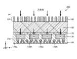
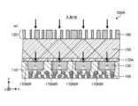
図26及び図27に示す撮像素子200は、画素アレイ110と光学素子アレイ120との間に設けられたフィルタ層170を備える。図26には、図2において撮像素子100を撮像素子200に置き換えた場合の、a-a´線に沿って側面視したときの撮像素子200の断面の例が示される。図27には、図2において撮像素子100を撮像素子100に置き換えた場合の、b-b´線に沿って側面視したときの撮像素子200の断面の例が示される。The
フィルタ層170は、画素Rを覆うように設けられ、赤の光を透過させるフィルタ170Rと、画素Gを覆うように設けられ、緑の光を透過させるフィルタ170Gと、画素Bを覆うように設けられ、青の光を透過させるフィルタ170Bと、画素NIRを覆うように設けられ、近赤外光を透過させるフィルタ170NIRとを含む。フィルタ層170の材料の例は、樹脂等の有機材料である。The
光学素子アレイ120によって色分離された光は、さらにフィルタ層170を通過してから、画素アレイ110に到達する。光学素子アレイ120及びフィルタ層170の両方の波長分離により、一方でのみ波長分離される場合よりも、スペクトルのクロストークが抑制され(不要な他の波長成分の大部分が除去され)、色再現性が向上する。また、入射した光は光学素子アレイ120で分離された後にフィルタ層170を通過するので、光量を大きく減少させることがない。したがって、光学素子アレイ120が無くフィルタ層170のみが設けられる場合と比較して、画素の受光効率が向上する。The light color-separated by the
図28は、図26及び図27に示す撮像素子200の各画素が受光する光のスペクトルの例を示す図である。図28には、構造体160がTiO2である場合のスペクトルの例が示される。 Fig. 28 is a diagram showing an example of the spectrum of light received by each pixel of the
図28では、画素Rの受光効率が、グラフ線Metalens×R filter (R)で示される。画素Gの受光効率が、グラフ線Metalens×G filter (G1 or G2)で示される。画素Bの受光効率が、グラフ線Metalens×R filter (B)で示される。画素NIRの受光効率が、グラフ線Metalens×R filter (NIR)で示される。比較例として、光学素子アレイ120が無く一般的なフィルタだけが設けられた場合の画素Rの受光効率が、グラフ線R filter (R)で示される。画素Gの受光効率が、グラフ線G filter (G1 or G2)で示される。画素Bの受光効率が、グラフ線B filter (B)で示される。画素NIRの受光効率が、グラフ線 filter (NIR)で示される。なお、比較例として併記したフィルタのみが設けられたRGB-IRセンサの各画素の感度スペクトルは、参考文献1を参照した。
参考文献1:Y. Monno, H. Teranaka, K. Yoshizaki, M. Tanaka, & M. Okutomi, (2018). “Single-sensor RGB-NIR imaging: High-quality system design and prototype implementation”. IEEE Sensors Journal, 19(2), 497-507. In FIG. 28, the light receiving efficiency of pixel R is shown by the graph line Metalens×R filter (R). The light receiving efficiency of pixel G is shown by the graph line Metalens×G filter (G1 or G2). The light receiving efficiency of pixel B is shown by the graph line Metalens×R filter (B). The light receiving efficiency of pixel NIR is shown by the graph line Metalens×R filter (NIR). As a comparative example, the light receiving efficiency of pixel R in the case where there is no
Reference 1: Y. Monno, H. Teranaka, K. Yoshizaki, M. Tanaka, & M. Okutomi, (2018). “Single-sensor RGB-NIR imaging: High-quality system design and prototype implementation”. IEEE Sensors Journal, 19(2), 497-507.
画素R、画素G、画素B及び画素NIRのスペクトルのピーク値は、比較例の1.5~1.9倍程度もあり、比較例よりも大きな受光効率が得られる。総透過率も39.4%であり、比較例の32.9%を上回る(約1.20倍)。さらに、各画素に入射する光のスペクトルも比較例のスペクトルよりシャープになっており、その分、不要な他の波長成分を減少できることも分かる。これにより、色再現性が高められる。The peak values of the spectra of pixel R, pixel G, pixel B and pixel NIR are approximately 1.5 to 1.9 times that of the comparative example, resulting in a higher light receiving efficiency than the comparative example. The total transmittance is also 39.4%, exceeding the 32.9% of the comparative example (approximately 1.20 times). Furthermore, the spectrum of the light incident on each pixel is sharper than that of the comparative example, which means that unnecessary other wavelength components can be reduced accordingly. This improves color reproducibility.
[実施の形態2の効果]
このように、フィルタ層170をさらに備える撮像素子200によれば、受光効率を向上させるとともに、色再現性をもさらに向上させることができる。[Effects of the second embodiment]
In this way, the
[実施の形態2の変形例]
図29~図32は、実施の形態2の変形例に係る撮像素子の概略構成の例を示す図である。図29及び図30の撮像素子200Aに示すように、フィルタ層170に代えて、近赤外吸収フィルタ170Aを設けてもよい。また、図31及び図32の撮像素子200Bに示すように、フィルタ層170の上(或いは下)に近赤外吸収フィルタ層170Aを設けてもよい。近赤外吸収フィルタ層170Aは、画素R、画素G及び画素Bのみの直上に、画素R、画素G及び画素Bのみを覆うように設けられた近赤外光を吸収するフィルタ170NIRを有する。このように、近赤外吸収フィルタ層170Aが、画素R、画素G、画素Bの直上のみに設けられることで、ノイズ要因となる近赤外光の画素R、画素G、画素Bへの入射を抑制することができる。なお、画素NIRについては、近赤外光の受光が必要であるため、画素NIR上にはフィルタ170NIRは設けられない。[Modification of the second embodiment]
29 to 32 are diagrams showing an example of a schematic configuration of an imaging element according to a modification of the second embodiment. As shown in the
なお、実施の形態1,2では、構造体160の材料として、TiO2及びSiNを例に挙げて説明した。ただし、構造体160の材料はそれらに限定されない。例えば、波長が380nm~1000nmの光(可視光~近赤外光)の光に対しては、SiNの他に、SiC、TiO2、GaN等が構造体6の材料として用いられてよい。屈折率が高く、吸収損失が少ないため適している。波長が800~1000nmの光(近赤外光)で用いる場合は、Si、SiC、SiN、TiO2、GaAs、GaN等が構造体6の材料として用いられてよい。低損失であるため適している。長波長帯の近赤外領域(通信波長である1.3μmや1.55μm等)の光に対しては、上述の材料に加えて、InP等を構造体160の材料として用いることができる。 In the first and second embodiments, TiO2 and SiN are used as examples of the material of the
また、構造体160が、貼り付け、塗布等によって形成される場合、フッ素化ポリイミド等のポリイミド、BCB(ベンゾシクロブテン)、光硬化性樹脂、UVエポキシ樹脂、PMMA等のアクリル樹脂、レジスト全般などのポリマー等が材料として挙げられる。In addition, when the
また、実施の形態1,2では、透明層150の材料としてSiO2及び空気層を想定した例を示したが、これらに限定されない。一般的なガラス材料等も含め、構造体160の材料の屈折率より低い屈折率を有し、入射光の波長に対して低損失なものであればよい。透明層150は、対応する画素に到達すべき光の波長に対して十分に低損失であればよいため、カラーフィルタと同様の材質であってもよく、例えば樹脂などの有機材料であってもよい。この場合、単に透明層150がカラーフィルタと同様の材質であるばかりでなく、カラーフィルタと同様の構造を持ち、対応する画素に導かれるべき光の波長に応じた吸収特性を持つよう設計されていてもよい。 In addition, in the first and second embodiments, an example was shown in which SiO2 and an air layer were assumed as the material of the
また、実施の形態1,2では、画素の対応する色として、RGBの3原色及び近赤外光を例に挙げて説明したが、画素は、近赤外光及び3原色以外の波長の光(例えば、赤外光、紫外光等)にも対応してよい。In addition, in the first and second embodiments, the three primary colors of RGB and near-infrared light have been given as examples of colors that the pixels can correspond to, but the pixels may also be compatible with light of wavelengths other than near-infrared light and the three primary colors (e.g., infrared light, ultraviolet light, etc.).
また、実施の形態1,2では、構造体160の形状として、正方形形状、×字形状、中空ひし形の異なる3種類の断面形状を有する構造体が用いられる例について説明した。この形状は一例であり、2種類の構造体(例えば正方形形状、×字形状のみ)が用いられてもよいし、4種類以上の構造体が用いられてもよい。In addition, in the first and second embodiments, an example has been described in which structures having three different cross-sectional shapes, a square shape, an X shape, and a hollow rhombus, are used as the shape of the
以上、本発明を具体的な実施の形態に基づいて説明したが、本発明は前記実施の形態に限定されるものではなく、その要旨を逸脱しない範囲において種々変更可能であることは言うまでもない。The present invention has been described above based on specific embodiments, but it goes without saying that the present invention is not limited to the above embodiments and can be modified in various ways without departing from the spirit of the invention.
以上説明した技術は、例えば次のように特定される。図1~図5、図23及び図24等を参照して説明したように、光学素子アレイ120は、各々が光電変換素子を含む複数の画素を覆うための透明層150と、透明層150上または透明層150内において透明層150の面方向(XY平面方向)に配置された複数の構造体160と、を備え、複数の構造体160は、入射した光のうち、波長が近赤外光領域である第1の光を前記複数の画素のうちの第1の画素(画素NIR)に集光し、波長が近赤外領域外の領域である第2の色(例えば、青)の光を第2の画素(例えば画素B)に集光するように配置される。The above-described technology can be specified, for example, as follows. As described with reference to Figures 1 to 5, 23, and 24, the
上記の光学素子アレイ120は、近赤外光領域の波長と他の領域の波長との分離機能及びレンズ機能(集光機能)の両方の機能を兼ね備える。したがって、例えば各画素に対応するフィルタ(例えばカラーフィルタ)を設けたり、さらにはマイクロレンズを設けたりする場合よりも、画素における、入射光の可視光と近赤外光との受光効率を大幅に向上させ、受光感度を向上させることができる。また、構造が簡素化されるため、製造コストを低減することもできる。複数の構造体160を面内に隙間なく配置できるため、マイクロレンズに比べて開口率も増加する。色分離機能及びレンズ機能は、近赤外光領域の波長と他の領域の波長とを分離集光する機能に限らず、近赤外光と、3色または2色の光とに対応していてもよい。The
図1~図5、図23及び図24等を参照して説明したように、光学素子アレイ120は、各々が光電変換素子を含む複数の画素を覆うための透明層150と、透明層150上または透明層150内において透明層150の面方向(平面方向)に配置された複数の構造体160と、を備え、入射した光のうち、近赤外光領域である第1の光を出力し、入射した光のうち、波長が前記近赤外領域外の領域である第2の色の光を出力してもよい。これによって、光学素子アレイ120は、近赤外光領域の波長と他の領域の波長との分離機能及を備える。As described with reference to Figures 1 to 5, 23 and 24, the
図10~図15等を参照して説明したように、複数の構造体160の各々は、透明層5の屈折率よりも高い屈折率を有し、入射した光に対して断面形状に応じた光位相遅延量を与える柱状構造体であってよい。図16~図21等を参照して説明したように、複数の構造体160は、上述の集光を実現するための光位相遅延量分布に従って配置されてよい。例えばこのような複数の構造体160の配置により、波長分離機能及びレンズ機能の両方の機能を実現することができる。As described with reference to Figures 10 to 15, each of the
図5及び図25等を参照して説明したように、複数の構造体160の各々の断面形状は、4回回転対称形状であってよい。これにより、偏光依存性が生じないようにすることができる。As described with reference to Figures 5 and 25, the cross-sectional shape of each of the
図6~図9等を参照して説明したように、複数の構造体6は、1つの画素と対向する領域の外側に入射した光のうちの当該1つの画素に対応する波長の光も当該1つの画素に集光するように配置されてよい。これにより、1つの画素と対向する領域に入射した光だけをその画素に集光する場合よりも、受光光量を増加させることができる。6 to 9, the
図1~図5等を参照して説明した撮像素子100も、本開示の一態様である。撮像素子100は、光学素子アレイ120と、透明層150で覆われた複数の画素130(画素NIR等)と、を備える。これにより、先にも説明したように、製造コストを低減することができる。受光感度を向上させたり、開口率を増加させたりすることもできる。The
図26及び図27等を参照して説明したように、撮像素子200は、複数の画素(画素NIR等)と透明層150との間に設けられたフィルタ層170を備えてよい。これにより、受光効率を向上させるとともに、色再現性をさらに向上させることができる。26 and 27, the
そして、図29~図32を参照して説明したように、撮像素子200A,200Bは、第2の画素上にのみ設けられた近赤外吸収フィルタ170Aを設けてもよい。第2の画素(画素R、画素G、画素B)の直上に、近赤外光を吸収する近赤外吸収フィルタを設けて、ノイズ要因となる近赤外光の第2の画素(画素R、画素G、画素B)への入射を抑制してもよい。29 to 32, the
図1等を参照して説明した撮像装置10も、本開示の一態様である。撮像装置10は、上述の撮像素子12と、撮像素子12から得られた電気信号に基づいて画素信号に基づいて画像信号を生成する信号処理部13と、を備える。これにより、先にも説明したように、製造コストを低減することができる。受光感度を向上させたり、開口率を増加させたりすることもできる。The imaging device 10 described with reference to FIG. 1 and the like is also one aspect of the present disclosure. The imaging device 10 includes the
1 物体
10 撮像装置
11 レンズ光学系
12,100,100A,100B,200 撮像素子
13 信号処理部
110 画素アレイ
120 光学素子アレイ
130 画素
150,150A 透明層
160 構造体
170 フィルタ層
180 配線層
190 透明基板 REFERENCE SIGNS
Claims (6)
Translated fromJapanese前記複数の画素を覆う透明層と、
前記透明層上または前記透明層内において前記透明層の面方向に配置された複数の構造体と、
を備える素子であって、
前記複数の構造体は、入射した光のうち、波長が近赤外光領域である第1の光を前記複数の画素のうちの第1の画素に集光し、波長が前記近赤外領域外の領域である第2の色の光を第2の画素に集光するように配置され、
前記複数の構造体は、1つの画素と対向する領域の外側に入射した光のうちの当該1つの画素に対応する波長の光も当該1つの画素に集光するように配置され、
前記入射した光を集光するためのマイクロレンズを含まずに構成されることを特徴とする撮像素子。 A plurality of pixels each including a photoelectric conversion element;
A transparent layer covering the plurality of pixels;
A plurality of structures arranged on or within the transparent layer in a surface direction of the transparent layer;
An element comprising:
the plurality of structures are arranged to collect, among the incident light, a first light having a wavelength in a near-infrared light region on a first pixel among the plurality of pixels, and collect, among the incident light, a second color light having a wavelength in a region outside the near-infrared light region on a second pixel;
the plurality of structures are arranged so as to collect, on one pixel, light having a wavelength corresponding to the one pixel among light incident on an area outside the one pixel;
An imaging element comprising: an imaging device configured without including a microlens for collecting the incident light.
前記複数の構造体は、前記集光を実現するための光位相量遅延分布に従って断面形状が設定され、前記集光を実現するための光位相量遅延分布に従って配置されることを特徴とする請求項1に記載の撮像素子。 each of the plurality of structures is a columnar structure having a refractive index higher than a refractive index of the transparent layer and imparting an optical phase delay amount corresponding to a cross-sectional shape to incident light;
The imaging element according to claim 1 , wherein the plurality of structures have cross-sectional shapes set in accordance with an optical phase delay distribution for achieving the focusing, and are arranged in accordance with the optical phasedelay distribution for achieving the focusing.
前記撮像素子から得られた電気信号に基づいて画像信号を生成する信号処理部と、
を備えることを特徴とする撮像装置。 An imaging element according toany one of claims 1 to 5 ,
a signal processing unit that generates an image signal based on the electrical signal obtained from the imaging element;
An imaging device comprising:
Applications Claiming Priority (1)
| Application Number | Priority Date | Filing Date | Title |
|---|---|---|---|
| PCT/JP2020/044561WO2022113363A1 (en) | 2020-11-30 | 2020-11-30 | Optical element, imaging element, and imaging device |
Publications (2)
| Publication Number | Publication Date |
|---|---|
| JPWO2022113363A1 JPWO2022113363A1 (en) | 2022-06-02 |
| JP7574860B2true JP7574860B2 (en) | 2024-10-29 |
Family
ID=81754195
Family Applications (1)
| Application Number | Title | Priority Date | Filing Date |
|---|---|---|---|
| JP2022565016AActiveJP7574860B2 (en) | 2020-11-30 | 2020-11-30 | Image pickup element and image pickup device |
Country Status (6)
| Country | Link |
|---|---|
| US (1) | US20240014237A1 (en) |
| EP (1) | EP4242703A4 (en) |
| JP (1) | JP7574860B2 (en) |
| KR (1) | KR102801193B1 (en) |
| CN (1) | CN116547565B (en) |
| WO (1) | WO2022113363A1 (en) |
Families Citing this family (5)
| Publication number | Priority date | Publication date | Assignee | Title |
|---|---|---|---|---|
| JP7574859B2 (en)* | 2020-11-30 | 2024-10-29 | 日本電信電話株式会社 | Image pickup element and image pickup device |
| WO2024157371A1 (en)* | 2023-01-25 | 2024-08-02 | 日本電信電話株式会社 | Solar battery module and conversion device |
| WO2025070228A1 (en)* | 2023-09-27 | 2025-04-03 | ソニーセミコンダクタソリューションズ株式会社 | Light detection device |
| WO2025079513A1 (en)* | 2023-10-11 | 2025-04-17 | ソニーセミコンダクタソリューションズ株式会社 | Imaging device and electronic device |
| WO2025164103A1 (en)* | 2024-01-31 | 2025-08-07 | ソニーセミコンダクタソリューションズ株式会社 | Light detection device, optical element, and electronic device |
Citations (6)
| Publication number | Priority date | Publication date | Assignee | Title |
|---|---|---|---|---|
| JP2010156942A (en) | 2008-12-31 | 2010-07-15 | Ind Technol Res Inst | Color dividing optical device and imaging device with the application |
| JP2017139286A (en) | 2016-02-02 | 2017-08-10 | ソニー株式会社 | Imaging element and camera system |
| JP2018146750A (en) | 2017-03-03 | 2018-09-20 | 株式会社ジャパンディスプレイ | Display device, displaying method, and color separation element |
| JP2019184986A (en) | 2018-04-17 | 2019-10-24 | 日本電信電話株式会社 | Color imaging device and imaging device |
| WO2020066738A1 (en) | 2018-09-26 | 2020-04-02 | 日本電信電話株式会社 | Polarization imaging system |
| JP2020123964A (en) | 2018-04-17 | 2020-08-13 | 日本電信電話株式会社 | Color imaging device and imaging apparatus |
Family Cites Families (17)
| Publication number | Priority date | Publication date | Assignee | Title |
|---|---|---|---|---|
| KR970004993B1 (en)* | 1992-05-01 | 1997-04-10 | 스미도모덴기고오교오 가부시기가이샤 | Method for identifying an optical fiber using a pattern of reflected light |
| CN100417230C (en)* | 2000-06-16 | 2008-09-03 | 夏普公司 | Projection type image display device |
| US6951393B2 (en)* | 2002-07-31 | 2005-10-04 | Canon Kabushiki Kaisha | Projection type image display apparatus and image display system |
| US7808023B2 (en)* | 2005-08-24 | 2010-10-05 | Aptina Imaging Corporation | Method and apparatus providing integrated color pixel with buried sub-wavelength gratings in solid state imagers |
| JP2008288243A (en)* | 2007-05-15 | 2008-11-27 | Sony Corp | Solid-state imaging device, manufacturing method thereof and imaging device |
| JP2011040441A (en)* | 2009-08-06 | 2011-02-24 | Panasonic Corp | Solid-state imaging apparatus |
| JP5227368B2 (en)* | 2010-06-02 | 2013-07-03 | パナソニック株式会社 | 3D imaging device |
| CN106405707B (en)* | 2011-06-06 | 2021-07-20 | Agc株式会社 | Optical filter, solid-state imaging element, lens for imaging device, and imaging device |
| JP2015028960A (en)* | 2011-12-01 | 2015-02-12 | ソニー株式会社 | Solid-state imaging device and electronic apparatus |
| WO2016013410A1 (en) | 2014-07-22 | 2016-01-28 | ソニー株式会社 | Solid-state imaging element, and electronic device |
| KR102465995B1 (en)* | 2015-09-30 | 2022-11-25 | 삼성전자주식회사 | Color splitter structure, method of manufacturing the same, image sensor including color splitter structure and optical apparatus including image sensor |
| JP2017212292A (en)* | 2016-05-24 | 2017-11-30 | 凸版印刷株式会社 | Solid-state image sensor |
| US10819922B2 (en)* | 2017-02-21 | 2020-10-27 | Nanolux Co. Ltd. | Solid-state imaging element and imaging device |
| WO2018225367A1 (en)* | 2017-06-09 | 2018-12-13 | ソニーセミコンダクタソリューションズ株式会社 | Solid-state imaging device |
| JP7222361B2 (en)* | 2018-02-05 | 2023-02-15 | Agc株式会社 | Optical filters and imagers |
| JP2020027937A (en)* | 2018-08-10 | 2020-02-20 | ブリルニクス インク | Solid-state imaging device, method of manufacturing solid-state imaging device, and electronic apparatus |
| JP7574859B2 (en)* | 2020-11-30 | 2024-10-29 | 日本電信電話株式会社 | Image pickup element and image pickup device |
- 2020
- 2020-11-30USUS18/039,040patent/US20240014237A1/enactivePending
- 2020-11-30KRKR1020237017917Apatent/KR102801193B1/enactiveActive
- 2020-11-30EPEP20963626.5Apatent/EP4242703A4/enactivePending
- 2020-11-30JPJP2022565016Apatent/JP7574860B2/enactiveActive
- 2020-11-30WOPCT/JP2020/044561patent/WO2022113363A1/ennot_activeCeased
- 2020-11-30CNCN202080107511.7Apatent/CN116547565B/enactiveActive
Patent Citations (6)
| Publication number | Priority date | Publication date | Assignee | Title |
|---|---|---|---|---|
| JP2010156942A (en) | 2008-12-31 | 2010-07-15 | Ind Technol Res Inst | Color dividing optical device and imaging device with the application |
| JP2017139286A (en) | 2016-02-02 | 2017-08-10 | ソニー株式会社 | Imaging element and camera system |
| JP2018146750A (en) | 2017-03-03 | 2018-09-20 | 株式会社ジャパンディスプレイ | Display device, displaying method, and color separation element |
| JP2019184986A (en) | 2018-04-17 | 2019-10-24 | 日本電信電話株式会社 | Color imaging device and imaging device |
| JP2020123964A (en) | 2018-04-17 | 2020-08-13 | 日本電信電話株式会社 | Color imaging device and imaging apparatus |
| WO2020066738A1 (en) | 2018-09-26 | 2020-04-02 | 日本電信電話株式会社 | Polarization imaging system |
Also Published As
| Publication number | Publication date |
|---|---|
| US20240014237A1 (en) | 2024-01-11 |
| WO2022113363A1 (en) | 2022-06-02 |
| CN116547565A (en) | 2023-08-04 |
| KR102801193B1 (en) | 2025-04-29 |
| EP4242703A1 (en) | 2023-09-13 |
| JPWO2022113363A1 (en) | 2022-06-02 |
| CN116547565B (en) | 2025-05-13 |
| KR20230093051A (en) | 2023-06-26 |
| EP4242703A4 (en) | 2024-07-24 |
Similar Documents
| Publication | Publication Date | Title |
|---|---|---|
| JP7574860B2 (en) | Image pickup element and image pickup device | |
| US8847345B2 (en) | Optical element, image sensor including the optical element, and image pickup apparatus including the image sensor | |
| KR102832511B1 (en) | Spectrophotometer array, imaging device and imaging device | |
| JP2024180638A (en) | Image pickup element and image pickup device | |
| US20250120207A1 (en) | Image capturing element and image capturing apparatus having spectroscopic element array | |
| JP7574858B2 (en) | Image pickup element and image pickup device | |
| JP7635787B2 (en) | Optical element, imaging element, and imaging device | |
| JP7563472B2 (en) | Optical element, imaging element, and imaging device | |
| US9257469B2 (en) | Color imaging device | |
| WO2023021632A1 (en) | Optical element, imaging element, and imaging device |
Legal Events
| Date | Code | Title | Description |
|---|---|---|---|
| A621 | Written request for application examination | Free format text:JAPANESE INTERMEDIATE CODE: A621 Effective date:20230323 | |
| A131 | Notification of reasons for refusal | Free format text:JAPANESE INTERMEDIATE CODE: A131 Effective date:20231010 | |
| A521 | Request for written amendment filed | Free format text:JAPANESE INTERMEDIATE CODE: A523 Effective date:20231211 | |
| A131 | Notification of reasons for refusal | Free format text:JAPANESE INTERMEDIATE CODE: A131 Effective date:20240305 | |
| A601 | Written request for extension of time | Free format text:JAPANESE INTERMEDIATE CODE: A601 Effective date:20240423 | |
| A521 | Request for written amendment filed | Free format text:JAPANESE INTERMEDIATE CODE: A523 Effective date:20240604 | |
| TRDD | Decision of grant or rejection written | ||
| A01 | Written decision to grant a patent or to grant a registration (utility model) | Free format text:JAPANESE INTERMEDIATE CODE: A01 Effective date:20240917 | |
| A61 | First payment of annual fees (during grant procedure) | Free format text:JAPANESE INTERMEDIATE CODE: A61 Effective date:20240930 | |
| R150 | Certificate of patent or registration of utility model | Ref document number:7574860 Country of ref document:JP Free format text:JAPANESE INTERMEDIATE CODE: R150 | |
| S533 | Written request for registration of change of name | Free format text:JAPANESE INTERMEDIATE CODE: R313533 |