JP7570385B2 - Semiconductor Device - Google Patents
Semiconductor DeviceDownload PDFInfo
- Publication number
- JP7570385B2 JP7570385B2JP2022154531AJP2022154531AJP7570385B2JP 7570385 B2JP7570385 B2JP 7570385B2JP 2022154531 AJP2022154531 AJP 2022154531AJP 2022154531 AJP2022154531 AJP 2022154531AJP 7570385 B2JP7570385 B2JP 7570385B2
- Authority
- JP
- Japan
- Prior art keywords
- oxide semiconductor
- region
- oxygen
- layer
- semiconductor layer
- Prior art date
- Legal status (The legal status is an assumption and is not a legal conclusion. Google has not performed a legal analysis and makes no representation as to the accuracy of the status listed.)
- Active
Links
- 239000004065semiconductorSubstances0.000titleclaimsdescription441
- 229910052760oxygenInorganic materials0.000claimsdescription185
- 239000001301oxygenSubstances0.000claimsdescription184
- QVGXLLKOCUKJST-UHFFFAOYSA-Natomic oxygenChemical compound[O]QVGXLLKOCUKJST-UHFFFAOYSA-N0.000claimsdescription183
- 230000015572biosynthetic processEffects0.000claimsdescription70
- 239000010936titaniumSubstances0.000claimsdescription45
- IJGRMHOSHXDMSA-UHFFFAOYSA-NAtomic nitrogenChemical compoundN#NIJGRMHOSHXDMSA-UHFFFAOYSA-N0.000claimsdescription40
- 239000001257hydrogenSubstances0.000claimsdescription35
- 229910052739hydrogenInorganic materials0.000claimsdescription35
- 229910052710siliconInorganic materials0.000claimsdescription26
- XUIMIQQOPSSXEZ-UHFFFAOYSA-NSiliconChemical compound[Si]XUIMIQQOPSSXEZ-UHFFFAOYSA-N0.000claimsdescription25
- 239000010703siliconSubstances0.000claimsdescription25
- 229910052719titaniumInorganic materials0.000claimsdescription24
- 230000006870functionEffects0.000claimsdescription20
- 229910052757nitrogenInorganic materials0.000claimsdescription20
- RTAQQCXQSZGOHL-UHFFFAOYSA-NTitaniumChemical compound[Ti]RTAQQCXQSZGOHL-UHFFFAOYSA-N0.000claimsdescription18
- UFHFLCQGNIYNRP-UHFFFAOYSA-NHydrogenChemical compound[H][H]UFHFLCQGNIYNRP-UHFFFAOYSA-N0.000claimsdescription17
- 150000002431hydrogenChemical class0.000claimsdescription17
- 239000011701zincSubstances0.000claimsdescription15
- 229910052738indiumInorganic materials0.000claimsdescription13
- 229910052750molybdenumInorganic materials0.000claimsdescription13
- 229910052733galliumInorganic materials0.000claimsdescription11
- 229910052721tungstenInorganic materials0.000claimsdescription11
- ZOKXTWBITQBERF-UHFFFAOYSA-NMolybdenumChemical compound[Mo]ZOKXTWBITQBERF-UHFFFAOYSA-N0.000claimsdescription10
- 239000011733molybdenumSubstances0.000claimsdescription10
- 239000010937tungstenSubstances0.000claimsdescription9
- 229910052725zincInorganic materials0.000claimsdescription9
- WFKWXMTUELFFGS-UHFFFAOYSA-NtungstenChemical compound[W]WFKWXMTUELFFGS-UHFFFAOYSA-N0.000claimsdescription8
- APFVFJFRJDLVQX-UHFFFAOYSA-Nindium atomChemical compound[In]APFVFJFRJDLVQX-UHFFFAOYSA-N0.000claimsdescription7
- 229910017052cobaltInorganic materials0.000claimsdescription6
- 239000010941cobaltSubstances0.000claimsdescription6
- GUTLYIVDDKVIGB-UHFFFAOYSA-Ncobalt atomChemical compound[Co]GUTLYIVDDKVIGB-UHFFFAOYSA-N0.000claimsdescription6
- 239000011368organic materialSubstances0.000claimsdescription4
- 239000004642PolyimideSubstances0.000claimsdescription2
- 229920001721polyimidePolymers0.000claimsdescription2
- HCHKCACWOHOZIP-UHFFFAOYSA-NZincChemical compound[Zn]HCHKCACWOHOZIP-UHFFFAOYSA-N0.000claims1
- 239000010410layerSubstances0.000description728
- 230000001939inductive effectEffects0.000description204
- 230000007547defectEffects0.000description122
- 239000010408filmSubstances0.000description113
- 239000000758substrateSubstances0.000description85
- 238000010438heat treatmentMethods0.000description83
- 238000000034methodMethods0.000description69
- 229910007541Zn OInorganic materials0.000description62
- 239000000463materialSubstances0.000description58
- 239000007789gasSubstances0.000description45
- 238000004544sputter depositionMethods0.000description40
- XKRFYHLGVUSROY-UHFFFAOYSA-NArgonChemical compound[Ar]XKRFYHLGVUSROY-UHFFFAOYSA-N0.000description36
- VYPSYNLAJGMNEJ-UHFFFAOYSA-Nsilicon dioxideInorganic materialsO=[Si]=OVYPSYNLAJGMNEJ-UHFFFAOYSA-N0.000description36
- 125000004429atomChemical group0.000description35
- 229910052751metalInorganic materials0.000description34
- 239000002184metalSubstances0.000description31
- 239000004973liquid crystal related substanceSubstances0.000description30
- 239000013078crystalSubstances0.000description28
- 229910052814silicon oxideInorganic materials0.000description27
- 238000004364calculation methodMethods0.000description25
- 238000004519manufacturing processMethods0.000description25
- 229910052782aluminiumInorganic materials0.000description23
- 239000012298atmosphereSubstances0.000description22
- 239000012535impuritySubstances0.000description22
- XLYOFNOQVPJJNP-UHFFFAOYSA-NwaterSubstancesOXLYOFNOQVPJJNP-UHFFFAOYSA-N0.000description22
- XAGFODPZIPBFFR-UHFFFAOYSA-NaluminiumChemical compound[Al]XAGFODPZIPBFFR-UHFFFAOYSA-N0.000description21
- 230000008569processEffects0.000description21
- 229910052581Si3N4Inorganic materials0.000description18
- 229910052786argonInorganic materials0.000description18
- HQVNEWCFYHHQES-UHFFFAOYSA-Nsilicon nitrideChemical compoundN12[Si]34N5[Si]62N3[Si]51N64HQVNEWCFYHHQES-UHFFFAOYSA-N0.000description18
- 239000002245particleSubstances0.000description15
- 238000005530etchingMethods0.000description14
- 229910019092Mg-OInorganic materials0.000description13
- 229910019395Mg—OInorganic materials0.000description13
- 239000010409thin filmSubstances0.000description13
- 239000011521glassSubstances0.000description12
- 239000000411inducerSubstances0.000description12
- 206010021143HypoxiaDiseases0.000description11
- 230000005684electric fieldEffects0.000description11
- 239000000203mixtureSubstances0.000description11
- GQPLMRYTRLFLPF-UHFFFAOYSA-NNitrous OxideChemical compound[O-][N+]#NGQPLMRYTRLFLPF-UHFFFAOYSA-N0.000description10
- 125000002887hydroxy groupChemical group[H]O*0.000description9
- -1tungsten nitrideChemical class0.000description9
- PMHQVHHXPFUNSP-UHFFFAOYSA-Mcopper(1+);methylsulfanylmethane;bromideChemical compoundBr[Cu].CSCPMHQVHHXPFUNSP-UHFFFAOYSA-M0.000description8
- 229910052734heliumInorganic materials0.000description8
- 239000001307heliumSubstances0.000description8
- SWQJXJOGLNCZEY-UHFFFAOYSA-Nhelium atomChemical compound[He]SWQJXJOGLNCZEY-UHFFFAOYSA-N0.000description8
- 238000005468ion implantationMethods0.000description8
- 239000000123paperSubstances0.000description8
- XLOMVQKBTHCTTD-UHFFFAOYSA-NZinc monoxideChemical compound[Zn]=OXLOMVQKBTHCTTD-UHFFFAOYSA-N0.000description7
- 239000000956alloySubstances0.000description7
- 230000018044dehydrationEffects0.000description7
- 238000006297dehydration reactionMethods0.000description7
- 238000006356dehydrogenation reactionMethods0.000description7
- 229910044991metal oxideInorganic materials0.000description7
- 150000004706metal oxidesChemical class0.000description7
- 239000012299nitrogen atmosphereSubstances0.000description7
- 235000012239silicon dioxideNutrition0.000description7
- NRTOMJZYCJJWKI-UHFFFAOYSA-NTitanium nitrideChemical compound[Ti]#NNRTOMJZYCJJWKI-UHFFFAOYSA-N0.000description6
- 230000001133accelerationEffects0.000description6
- 229910045601alloyInorganic materials0.000description6
- 230000000694effectsEffects0.000description6
- 239000011261inert gasSubstances0.000description6
- 229910052754neonInorganic materials0.000description6
- GKAOGPIIYCISHV-UHFFFAOYSA-Nneon atomChemical compound[Ne]GKAOGPIIYCISHV-UHFFFAOYSA-N0.000description6
- 150000004767nitridesChemical class0.000description6
- ZOXJGFHDIHLPTG-UHFFFAOYSA-NBoronChemical compound[B]ZOXJGFHDIHLPTG-UHFFFAOYSA-N0.000description5
- 229910052796boronInorganic materials0.000description5
- 239000000969carrierSubstances0.000description5
- 239000003086colorantSubstances0.000description5
- 229910052802copperInorganic materials0.000description5
- 239000010949copperSubstances0.000description5
- 230000005669field effectEffects0.000description5
- 150000002500ionsChemical class0.000description5
- 239000003094microcapsuleSubstances0.000description5
- 238000000329molecular dynamics simulationMethods0.000description5
- TWNQGVIAIRXVLR-UHFFFAOYSA-Noxo(oxoalumanyloxy)alumaneChemical compoundO=[Al]O[Al]=OTWNQGVIAIRXVLR-UHFFFAOYSA-N0.000description5
- 238000012545processingMethods0.000description5
- 239000010453quartzSubstances0.000description5
- 239000000565sealantSubstances0.000description5
- 239000000126substanceSubstances0.000description5
- JBQYATWDVHIOAR-UHFFFAOYSA-NtellanylidenegermaniumChemical compound[Te]=[Ge]JBQYATWDVHIOAR-UHFFFAOYSA-N0.000description5
- RYGMFSIKBFXOCR-UHFFFAOYSA-NCopperChemical compound[Cu]RYGMFSIKBFXOCR-UHFFFAOYSA-N0.000description4
- MYMOFIZGZYHOMD-UHFFFAOYSA-NDioxygenChemical compoundO=OMYMOFIZGZYHOMD-UHFFFAOYSA-N0.000description4
- MHAJPDPJQMAIIY-UHFFFAOYSA-NHydrogen peroxideChemical compoundOOMHAJPDPJQMAIIY-UHFFFAOYSA-N0.000description4
- 229910020923Sn-OInorganic materials0.000description4
- 238000004891communicationMethods0.000description4
- 150000001875compoundsChemical class0.000description4
- 238000000151depositionMethods0.000description4
- 230000008021depositionEffects0.000description4
- 229910001882dioxygenInorganic materials0.000description4
- 150000004678hydridesChemical class0.000description4
- 125000004435hydrogen atomChemical group[H]*0.000description4
- 238000005268plasma chemical vapour depositionMethods0.000description4
- 239000002356single layerSubstances0.000description4
- 238000001179sorption measurementMethods0.000description4
- 238000003860storageMethods0.000description4
- 229910052715tantalumInorganic materials0.000description4
- VZGDMQKNWNREIO-UHFFFAOYSA-NtetrachloromethaneChemical compoundClC(Cl)(Cl)ClVZGDMQKNWNREIO-UHFFFAOYSA-N0.000description4
- XOLBLPGZBRYERU-UHFFFAOYSA-Ntin dioxideChemical compoundO=[Sn]=OXOLBLPGZBRYERU-UHFFFAOYSA-N0.000description4
- QTBSBXVTEAMEQO-UHFFFAOYSA-NAcetic acidChemical compoundCC(O)=OQTBSBXVTEAMEQO-UHFFFAOYSA-N0.000description3
- ZAMOUSCENKQFHK-UHFFFAOYSA-NChlorine atomChemical compound[Cl]ZAMOUSCENKQFHK-UHFFFAOYSA-N0.000description3
- XPDWGBQVDMORPB-UHFFFAOYSA-NFluoroformChemical compoundFC(F)FXPDWGBQVDMORPB-UHFFFAOYSA-N0.000description3
- 239000003990capacitorSubstances0.000description3
- 239000000460chlorineSubstances0.000description3
- 229910052801chlorineInorganic materials0.000description3
- 238000009826distributionMethods0.000description3
- 238000001312dry etchingMethods0.000description3
- 239000000428dustSubstances0.000description3
- 238000005516engineering processMethods0.000description3
- 229910003437indium oxideInorganic materials0.000description3
- PJXISJQVUVHSOJ-UHFFFAOYSA-Nindium(iii) oxideChemical compound[O-2].[O-2].[O-2].[In+3].[In+3]PJXISJQVUVHSOJ-UHFFFAOYSA-N0.000description3
- 239000007788liquidSubstances0.000description3
- 230000007246mechanismEffects0.000description3
- 150000002739metalsChemical class0.000description3
- 230000003287optical effectEffects0.000description3
- 150000002894organic compoundsChemical class0.000description3
- 125000004430oxygen atomChemical groupO*0.000description3
- 238000000206photolithographyMethods0.000description3
- 230000004044responseEffects0.000description3
- 238000001039wet etchingMethods0.000description3
- 239000011787zinc oxideSubstances0.000description3
- UWCWUCKPEYNDNV-LBPRGKRZSA-N2,6-dimethyl-n-[[(2s)-pyrrolidin-2-yl]methyl]anilineChemical compoundCC1=CC=CC(C)=C1NC[C@H]1NCCC1UWCWUCKPEYNDNV-LBPRGKRZSA-N0.000description2
- VXEGSRKPIUDPQT-UHFFFAOYSA-N4-[4-(4-methoxyphenyl)piperazin-1-yl]anilineChemical compoundC1=CC(OC)=CC=C1N1CCN(C=2C=CC(N)=CC=2)CC1VXEGSRKPIUDPQT-UHFFFAOYSA-N0.000description2
- QGZKDVFQNNGYKY-UHFFFAOYSA-NAmmoniaChemical compoundNQGZKDVFQNNGYKY-UHFFFAOYSA-N0.000description2
- 238000003775Density Functional TheoryMethods0.000description2
- YCKRFDGAMUMZLT-UHFFFAOYSA-NFluorine atomChemical compound[F]YCKRFDGAMUMZLT-UHFFFAOYSA-N0.000description2
- CPELXLSAUQHCOX-UHFFFAOYSA-NHydrogen bromideChemical compoundBrCPELXLSAUQHCOX-UHFFFAOYSA-N0.000description2
- 229910052779NeodymiumInorganic materials0.000description2
- NBIIXXVUZAFLBC-UHFFFAOYSA-NPhosphoric acidChemical compoundOP(O)(O)=ONBIIXXVUZAFLBC-UHFFFAOYSA-N0.000description2
- 239000012300argon atmosphereSubstances0.000description2
- 229910052785arsenicInorganic materials0.000description2
- RQNWIZPPADIBDY-UHFFFAOYSA-Narsenic atomChemical compound[As]RQNWIZPPADIBDY-UHFFFAOYSA-N0.000description2
- 230000003098cholesteric effectEffects0.000description2
- 229910052804chromiumInorganic materials0.000description2
- 239000011651chromiumSubstances0.000description2
- 229910052681coesiteInorganic materials0.000description2
- 229910052906cristobaliteInorganic materials0.000description2
- 238000002425crystallisationMethods0.000description2
- 230000008025crystallizationEffects0.000description2
- 238000013461designMethods0.000description2
- 238000010586diagramMethods0.000description2
- 238000005401electroluminescenceMethods0.000description2
- 230000005281excited stateEffects0.000description2
- 230000001747exhibiting effectEffects0.000description2
- 238000011049fillingMethods0.000description2
- 229910052731fluorineInorganic materials0.000description2
- 239000011737fluorineSubstances0.000description2
- 238000002513implantationMethods0.000description2
- 239000011810insulating materialSubstances0.000description2
- 229910052748manganeseInorganic materials0.000description2
- 239000011572manganeseSubstances0.000description2
- QKCGXXHCELUCKW-UHFFFAOYSA-Nn-[4-[4-(dinaphthalen-2-ylamino)phenyl]phenyl]-n-naphthalen-2-ylnaphthalen-2-amineChemical compoundC1=CC=CC2=CC(N(C=3C=CC(=CC=3)C=3C=CC(=CC=3)N(C=3C=C4C=CC=CC4=CC=3)C=3C=C4C=CC=CC4=CC=3)C3=CC4=CC=CC=C4C=C3)=CC=C21QKCGXXHCELUCKW-UHFFFAOYSA-N0.000description2
- 239000001272nitrous oxideSubstances0.000description2
- 239000004033plasticSubstances0.000description2
- 230000005855radiationEffects0.000description2
- 230000002441reversible effectEffects0.000description2
- 229910052706scandiumInorganic materials0.000description2
- 239000000377silicon dioxideSubstances0.000description2
- 239000005049silicon tetrachlorideSubstances0.000description2
- 239000002904solventSubstances0.000description2
- 239000012798spherical particleSubstances0.000description2
- 229910052682stishoviteInorganic materials0.000description2
- TXEYQDLBPFQVAA-UHFFFAOYSA-NtetrafluoromethaneChemical compoundFC(F)(F)FTXEYQDLBPFQVAA-UHFFFAOYSA-N0.000description2
- XJDNKRIXUMDJCW-UHFFFAOYSA-Jtitanium tetrachlorideChemical compoundCl[Ti](Cl)(Cl)ClXJDNKRIXUMDJCW-UHFFFAOYSA-J0.000description2
- 230000007704transitionEffects0.000description2
- FAQYAMRNWDIXMY-UHFFFAOYSA-NtrichloroboraneChemical compoundClB(Cl)ClFAQYAMRNWDIXMY-UHFFFAOYSA-N0.000description2
- 229910052905tridymiteInorganic materials0.000description2
- 239000002699waste materialSubstances0.000description2
- VHUUQVKOLVNVRT-UHFFFAOYSA-NAmmonium hydroxideChemical compound[NH4+].[OH-]VHUUQVKOLVNVRT-UHFFFAOYSA-N0.000description1
- FIPWRIJSWJWJAI-UHFFFAOYSA-NButyl carbitol 6-propylpiperonyl etherChemical compoundC1=C(CCC)C(COCCOCCOCCCC)=CC2=C1OCO2FIPWRIJSWJWJAI-UHFFFAOYSA-N0.000description1
- OKTJSMMVPCPJKN-UHFFFAOYSA-NCarbonChemical compound[C]OKTJSMMVPCPJKN-UHFFFAOYSA-N0.000description1
- VEXZGXHMUGYJMC-UHFFFAOYSA-MChloride anionChemical compound[Cl-]VEXZGXHMUGYJMC-UHFFFAOYSA-M0.000description1
- KZBUYRJDOAKODT-UHFFFAOYSA-NChlorineChemical compoundClClKZBUYRJDOAKODT-UHFFFAOYSA-N0.000description1
- 239000004986Cholesteric liquid crystals (ChLC)Substances0.000description1
- VYZAMTAEIAYCRO-UHFFFAOYSA-NChromiumChemical compound[Cr]VYZAMTAEIAYCRO-UHFFFAOYSA-N0.000description1
- YZCKVEUIGOORGS-OUBTZVSYSA-NDeuteriumChemical compound[2H]YZCKVEUIGOORGS-OUBTZVSYSA-N0.000description1
- 239000004593EpoxySubstances0.000description1
- KRHYYFGTRYWZRS-UHFFFAOYSA-MFluoride anionChemical compound[F-]KRHYYFGTRYWZRS-UHFFFAOYSA-M0.000description1
- GYHNNYVSQQEPJS-UHFFFAOYSA-NGalliumChemical compound[Ga]GYHNNYVSQQEPJS-UHFFFAOYSA-N0.000description1
- 239000005264High molar mass liquid crystalSubstances0.000description1
- DGAQECJNVWCQMB-PUAWFVPOSA-MIlexoside XXIXChemical compoundC[C@@H]1CC[C@@]2(CC[C@@]3(C(=CC[C@H]4[C@]3(CC[C@@H]5[C@@]4(CC[C@@H](C5(C)C)OS(=O)(=O)[O-])C)C)[C@@H]2[C@]1(C)O)C)C(=O)O[C@H]6[C@@H]([C@H]([C@@H]([C@H](O6)CO)O)O)O.[Na+]DGAQECJNVWCQMB-PUAWFVPOSA-M0.000description1
- 108010083687Ion PumpsProteins0.000description1
- 238000004510Lennard-Jones potentialMethods0.000description1
- FYYHWMGAXLPEAU-UHFFFAOYSA-NMagnesiumChemical compound[Mg]FYYHWMGAXLPEAU-UHFFFAOYSA-N0.000description1
- 238000000342Monte Carlo simulationMethods0.000description1
- GRYLNZFGIOXLOG-UHFFFAOYSA-NNitric acidChemical compoundO[N+]([O-])=OGRYLNZFGIOXLOG-UHFFFAOYSA-N0.000description1
- OAICVXFJPJFONN-UHFFFAOYSA-NPhosphorusChemical compound[P]OAICVXFJPJFONN-UHFFFAOYSA-N0.000description1
- 239000004952PolyamideSubstances0.000description1
- 239000004983Polymer Dispersed Liquid CrystalSubstances0.000description1
- 229910018503SF6Inorganic materials0.000description1
- 229910004304SiNyInorganic materials0.000description1
- 239000004990Smectic liquid crystalSubstances0.000description1
- 229910020944Sn-MgInorganic materials0.000description1
- 229910020994Sn-ZnInorganic materials0.000description1
- 229910009069Sn—ZnInorganic materials0.000description1
- 239000004974Thermotropic liquid crystalSubstances0.000description1
- QCWXUUIWCKQGHC-UHFFFAOYSA-NZirconiumChemical compound[Zr]QCWXUUIWCKQGHC-UHFFFAOYSA-N0.000description1
- QRSFFHRCBYCWBS-UHFFFAOYSA-N[O].[O]Chemical compound[O].[O]QRSFFHRCBYCWBS-UHFFFAOYSA-N0.000description1
- AZWHFTKIBIQKCA-UHFFFAOYSA-N[Sn+2]=O.[O-2].[In+3]Chemical compound[Sn+2]=O.[O-2].[In+3]AZWHFTKIBIQKCA-UHFFFAOYSA-N0.000description1
- NIXOWILDQLNWCW-UHFFFAOYSA-Nacrylic acid groupChemical groupC(C=C)(=O)ONIXOWILDQLNWCW-UHFFFAOYSA-N0.000description1
- 229910000147aluminium phosphateInorganic materials0.000description1
- 239000005407aluminoborosilicate glassSubstances0.000description1
- 239000005354aluminosilicate glassSubstances0.000description1
- 229910021529ammoniaInorganic materials0.000description1
- 235000011114ammonium hydroxideNutrition0.000description1
- 238000000137annealingMethods0.000description1
- 229910052788bariumInorganic materials0.000description1
- DSAJWYNOEDNPEQ-UHFFFAOYSA-Nbarium atomChemical compound[Ba]DSAJWYNOEDNPEQ-UHFFFAOYSA-N0.000description1
- QVQLCTNNEUAWMS-UHFFFAOYSA-Nbarium oxideChemical compound[Ba]=OQVQLCTNNEUAWMS-UHFFFAOYSA-N0.000description1
- UMIVXZPTRXBADB-UHFFFAOYSA-NbenzocyclobuteneChemical compoundC1=CC=C2CCC2=C1UMIVXZPTRXBADB-UHFFFAOYSA-N0.000description1
- 229910052790berylliumInorganic materials0.000description1
- ATBAMAFKBVZNFJ-UHFFFAOYSA-Nberyllium atomChemical compound[Be]ATBAMAFKBVZNFJ-UHFFFAOYSA-N0.000description1
- 239000011230binding agentSubstances0.000description1
- 229910052795boron group elementInorganic materials0.000description1
- 239000005380borophosphosilicate glassSubstances0.000description1
- 239000005388borosilicate glassSubstances0.000description1
- 229910052799carbonInorganic materials0.000description1
- 125000004432carbon atomChemical groupC*0.000description1
- 230000015556catabolic processEffects0.000description1
- 239000000919ceramicSubstances0.000description1
- 230000008859changeEffects0.000description1
- 239000002131composite materialSubstances0.000description1
- 239000004020conductorSubstances0.000description1
- 239000002826coolantSubstances0.000description1
- 238000001816coolingMethods0.000description1
- 230000007423decreaseEffects0.000description1
- 229910052805deuteriumInorganic materials0.000description1
- 238000009792diffusion processMethods0.000description1
- KPUWHANPEXNPJT-UHFFFAOYSA-NdisiloxaneChemical class[SiH3]O[SiH3]KPUWHANPEXNPJT-UHFFFAOYSA-N0.000description1
- 230000005611electricityEffects0.000description1
- 239000004744fabricSubstances0.000description1
- 239000005262ferroelectric liquid crystals (FLCs)Substances0.000description1
- QZQVBEXLDFYHSR-UHFFFAOYSA-Ngallium(III) oxideInorganic materialsO=[Ga]O[Ga]=OQZQVBEXLDFYHSR-UHFFFAOYSA-N0.000description1
- 230000005283ground stateEffects0.000description1
- 229910000449hafnium oxideInorganic materials0.000description1
- WIHZLLGSGQNAGK-UHFFFAOYSA-Nhafnium(4+);oxygen(2-)Chemical compound[O-2].[O-2].[Hf+4]WIHZLLGSGQNAGK-UHFFFAOYSA-N0.000description1
- 229910052736halogenInorganic materials0.000description1
- 150000002367halogensChemical class0.000description1
- 229910000042hydrogen bromideInorganic materials0.000description1
- 150000002483hydrogen compoundsChemical class0.000description1
- 150000002484inorganic compoundsChemical class0.000description1
- 229910010272inorganic materialInorganic materials0.000description1
- 238000003780insertionMethods0.000description1
- 230000037431insertionEffects0.000description1
- 239000011777magnesiumSubstances0.000description1
- 229910052749magnesiumInorganic materials0.000description1
- 239000000696magnetic materialSubstances0.000description1
- WPBNNNQJVZRUHP-UHFFFAOYSA-Lmanganese(2+);methyl n-[[2-(methoxycarbonylcarbamothioylamino)phenyl]carbamothioyl]carbamate;n-[2-(sulfidocarbothioylamino)ethyl]carbamodithioateChemical compound[Mn+2].[S-]C(=S)NCCNC([S-])=S.COC(=O)NC(=S)NC1=CC=CC=C1NC(=S)NC(=O)OCWPBNNNQJVZRUHP-UHFFFAOYSA-L0.000description1
- 239000011159matrix materialSubstances0.000description1
- 230000008018meltingEffects0.000description1
- 238000002844meltingMethods0.000description1
- QSHDDOUJBYECFT-UHFFFAOYSA-NmercuryChemical compound[Hg]QSHDDOUJBYECFT-UHFFFAOYSA-N0.000description1
- 229910052753mercuryInorganic materials0.000description1
- 229910001507metal halideInorganic materials0.000description1
- 150000005309metal halidesChemical class0.000description1
- 229910021645metal ionInorganic materials0.000description1
- 239000007769metal materialSubstances0.000description1
- 238000006263metalation reactionMethods0.000description1
- QEFYFXOXNSNQGX-UHFFFAOYSA-Nneodymium atomChemical compound[Nd]QEFYFXOXNSNQGX-UHFFFAOYSA-N0.000description1
- 229910017604nitric acidInorganic materials0.000description1
- 238000007645offset printingMethods0.000description1
- 239000003921oilSubstances0.000description1
- 238000005457optimizationMethods0.000description1
- MOWNZPNSYMGTMD-UHFFFAOYSA-NoxidoboronChemical compoundO=[B]MOWNZPNSYMGTMD-UHFFFAOYSA-N0.000description1
- 229910052698phosphorusInorganic materials0.000description1
- 239000011574phosphorusSubstances0.000description1
- 239000000049pigmentSubstances0.000description1
- 230000010287polarizationEffects0.000description1
- 229920002647polyamidePolymers0.000description1
- 239000000843powderSubstances0.000description1
- 230000000750progressive effectEffects0.000description1
- 238000004698pseudo-potential methodMethods0.000description1
- 238000010791quenchingMethods0.000description1
- 230000006798recombinationEffects0.000description1
- 238000005215recombinationMethods0.000description1
- 239000011347resinSubstances0.000description1
- 229920005989resinPolymers0.000description1
- 229910052594sapphireInorganic materials0.000description1
- 239000010980sapphireSubstances0.000description1
- SIXSYDAISGFNSX-UHFFFAOYSA-Nscandium atomChemical compound[Sc]SIXSYDAISGFNSX-UHFFFAOYSA-N0.000description1
- 238000007650screen-printingMethods0.000description1
- LIVNPJMFVYWSIS-UHFFFAOYSA-Nsilicon monoxideChemical compound[Si-]#[O+]LIVNPJMFVYWSIS-UHFFFAOYSA-N0.000description1
- 239000011734sodiumSubstances0.000description1
- 229910052708sodiumInorganic materials0.000description1
- 239000007787solidSubstances0.000description1
- 238000005507sprayingMethods0.000description1
- 230000003068static effectEffects0.000description1
- 238000000859sublimationMethods0.000description1
- 230000008022sublimationEffects0.000description1
- SFZCNBIFKDRMGX-UHFFFAOYSA-Nsulfur hexafluorideChemical compoundFS(F)(F)(F)(F)FSFZCNBIFKDRMGX-UHFFFAOYSA-N0.000description1
- 229960000909sulfur hexafluorideDrugs0.000description1
- GUVRBAGPIYLISA-UHFFFAOYSA-Ntantalum atomChemical compound[Ta]GUVRBAGPIYLISA-UHFFFAOYSA-N0.000description1
- MZLGASXMSKOWSE-UHFFFAOYSA-Ntantalum nitrideChemical compound[Ta]#NMZLGASXMSKOWSE-UHFFFAOYSA-N0.000description1
- 229910001887tin oxideInorganic materials0.000description1
- 230000008016vaporizationEffects0.000description1
- 238000005406washingMethods0.000description1
- 229910052724xenonInorganic materials0.000description1
- FHNFHKCVQCLJFQ-UHFFFAOYSA-Nxenon atomChemical compound[Xe]FHNFHKCVQCLJFQ-UHFFFAOYSA-N0.000description1
- 229910052727yttriumInorganic materials0.000description1
- OYQCBJZGELKKPM-UHFFFAOYSA-Nzinc indium(3+) oxygen(2-)Chemical compound[O-2].[Zn+2].[O-2].[In+3]OYQCBJZGELKKPM-UHFFFAOYSA-N0.000description1
- 229910052726zirconiumInorganic materials0.000description1
Images


Classifications
- H—ELECTRICITY
- H10—SEMICONDUCTOR DEVICES; ELECTRIC SOLID-STATE DEVICES NOT OTHERWISE PROVIDED FOR
- H10D—INORGANIC ELECTRIC SEMICONDUCTOR DEVICES
- H10D30/00—Field-effect transistors [FET]
- H10D30/60—Insulated-gate field-effect transistors [IGFET]
- H10D30/67—Thin-film transistors [TFT]
- H10D30/674—Thin-film transistors [TFT] characterised by the active materials
- H10D30/6755—Oxide semiconductors, e.g. zinc oxide, copper aluminium oxide or cadmium stannate
- H—ELECTRICITY
- H01—ELECTRIC ELEMENTS
- H01L—SEMICONDUCTOR DEVICES NOT COVERED BY CLASS H10
- H01L21/00—Processes or apparatus adapted for the manufacture or treatment of semiconductor or solid state devices or of parts thereof
- H01L21/02—Manufacture or treatment of semiconductor devices or of parts thereof
- H01L21/02104—Forming layers
- H01L21/02365—Forming inorganic semiconducting materials on a substrate
- H01L21/02518—Deposited layers
- H01L21/02521—Materials
- H01L21/02551—Group 12/16 materials
- H01L21/02554—Oxides
- H—ELECTRICITY
- H01—ELECTRIC ELEMENTS
- H01L—SEMICONDUCTOR DEVICES NOT COVERED BY CLASS H10
- H01L21/00—Processes or apparatus adapted for the manufacture or treatment of semiconductor or solid state devices or of parts thereof
- H01L21/02—Manufacture or treatment of semiconductor devices or of parts thereof
- H01L21/02104—Forming layers
- H01L21/02365—Forming inorganic semiconducting materials on a substrate
- H01L21/02518—Deposited layers
- H01L21/02521—Materials
- H01L21/02565—Oxide semiconducting materials not being Group 12/16 materials, e.g. ternary compounds
- H—ELECTRICITY
- H01—ELECTRIC ELEMENTS
- H01L—SEMICONDUCTOR DEVICES NOT COVERED BY CLASS H10
- H01L21/00—Processes or apparatus adapted for the manufacture or treatment of semiconductor or solid state devices or of parts thereof
- H01L21/02—Manufacture or treatment of semiconductor devices or of parts thereof
- H01L21/02104—Forming layers
- H01L21/02365—Forming inorganic semiconducting materials on a substrate
- H01L21/02612—Formation types
- H01L21/02617—Deposition types
- H01L21/02631—Physical deposition at reduced pressure, e.g. MBE, sputtering, evaporation
- H—ELECTRICITY
- H01—ELECTRIC ELEMENTS
- H01L—SEMICONDUCTOR DEVICES NOT COVERED BY CLASS H10
- H01L21/00—Processes or apparatus adapted for the manufacture or treatment of semiconductor or solid state devices or of parts thereof
- H01L21/02—Manufacture or treatment of semiconductor devices or of parts thereof
- H01L21/04—Manufacture or treatment of semiconductor devices or of parts thereof the devices having potential barriers, e.g. a PN junction, depletion layer or carrier concentration layer
- H01L21/34—Manufacture or treatment of semiconductor devices or of parts thereof the devices having potential barriers, e.g. a PN junction, depletion layer or carrier concentration layer the devices having semiconductor bodies not provided for in groups H01L21/18, H10D48/04 and H10D48/07, with or without impurities, e.g. doping materials
- H01L21/42—Bombardment with radiation
- H01L21/423—Bombardment with radiation with high-energy radiation
- H01L21/425—Bombardment with radiation with high-energy radiation producing ion implantation
- H01L21/426—Bombardment with radiation with high-energy radiation producing ion implantation using masks
- H—ELECTRICITY
- H10—SEMICONDUCTOR DEVICES; ELECTRIC SOLID-STATE DEVICES NOT OTHERWISE PROVIDED FOR
- H10D—INORGANIC ELECTRIC SEMICONDUCTOR DEVICES
- H10D62/00—Semiconductor bodies, or regions thereof, of devices having potential barriers
- H10D62/60—Impurity distributions or concentrations
- H—ELECTRICITY
- H10—SEMICONDUCTOR DEVICES; ELECTRIC SOLID-STATE DEVICES NOT OTHERWISE PROVIDED FOR
- H10D—INORGANIC ELECTRIC SEMICONDUCTOR DEVICES
- H10D62/00—Semiconductor bodies, or regions thereof, of devices having potential barriers
- H10D62/80—Semiconductor bodies, or regions thereof, of devices having potential barriers characterised by the materials
- H—ELECTRICITY
- H10—SEMICONDUCTOR DEVICES; ELECTRIC SOLID-STATE DEVICES NOT OTHERWISE PROVIDED FOR
- H10D—INORGANIC ELECTRIC SEMICONDUCTOR DEVICES
- H10D84/00—Integrated devices formed in or on semiconductor substrates that comprise only semiconducting layers, e.g. on Si wafers or on GaAs-on-Si wafers
- H10D84/01—Manufacture or treatment
- H10D84/0123—Integrating together multiple components covered by H10D12/00 or H10D30/00, e.g. integrating multiple IGBTs
- H10D84/0126—Integrating together multiple components covered by H10D12/00 or H10D30/00, e.g. integrating multiple IGBTs the components including insulated gates, e.g. IGFETs
- H10D84/013—Manufacturing their source or drain regions, e.g. silicided source or drain regions
- H—ELECTRICITY
- H10—SEMICONDUCTOR DEVICES; ELECTRIC SOLID-STATE DEVICES NOT OTHERWISE PROVIDED FOR
- H10D—INORGANIC ELECTRIC SEMICONDUCTOR DEVICES
- H10D84/00—Integrated devices formed in or on semiconductor substrates that comprise only semiconducting layers, e.g. on Si wafers or on GaAs-on-Si wafers
- H10D84/01—Manufacture or treatment
- H10D84/02—Manufacture or treatment characterised by using material-based technologies
- H10D84/03—Manufacture or treatment characterised by using material-based technologies using Group IV technology, e.g. silicon technology or silicon-carbide [SiC] technology
- H10D84/038—Manufacture or treatment characterised by using material-based technologies using Group IV technology, e.g. silicon technology or silicon-carbide [SiC] technology using silicon technology, e.g. SiGe
- H—ELECTRICITY
- H10—SEMICONDUCTOR DEVICES; ELECTRIC SOLID-STATE DEVICES NOT OTHERWISE PROVIDED FOR
- H10D—INORGANIC ELECTRIC SEMICONDUCTOR DEVICES
- H10D99/00—Subject matter not provided for in other groups of this subclass
Landscapes
- Engineering & Computer Science (AREA)
- Microelectronics & Electronic Packaging (AREA)
- Computer Hardware Design (AREA)
- Power Engineering (AREA)
- Condensed Matter Physics & Semiconductors (AREA)
- General Physics & Mathematics (AREA)
- Manufacturing & Machinery (AREA)
- Physics & Mathematics (AREA)
- Health & Medical Sciences (AREA)
- Toxicology (AREA)
- Thin Film Transistor (AREA)
- Liquid Crystal (AREA)
- Recrystallisation Techniques (AREA)
- Electrodes Of Semiconductors (AREA)
- Devices For Indicating Variable Information By Combining Individual Elements (AREA)
- Electroluminescent Light Sources (AREA)
Description
Translated fromJapanese酸化物半導体を用いる半導体装置及びその作製方法に関する。This relates to a semiconductor device using an oxide semiconductor and a method for manufacturing the same.
なお、本明細書中において半導体装置とは、半導体特性を利用することで機能しうる装置
全般を指し、電気光学装置、半導体回路および電子機器は全て半導体装置である。In this specification, the term "semiconductor device" refers to any device that can function by utilizing semiconductor characteristics, and electro-optical devices, semiconductor circuits, and electronic devices are all classified as semiconductor devices.
絶縁表面を有する基板上に形成された半導体薄膜を用いて薄膜トランジスタ(TFT)を
構成する技術が注目されている。薄膜トランジスタや電気光学装置のような電子デバイス
に広く応用されている。薄膜トランジスタに適用可能な半導体薄膜としてシリコン系半導
体材料が公知であるが、その他の材料として酸化物半導体が注目されている。A technology for constructing thin film transistors (TFTs) using a semiconductor thin film formed on a substrate having an insulating surface has been attracting attention. This technology is widely applied to electronic devices such as thin film transistors and electro-optical devices. Silicon-based semiconductor materials are well known as semiconductor thin films applicable to thin film transistors, but oxide semiconductors have also been attracting attention as other materials.
酸化物半導体を用いたトランジスタとしては、より高機能な半導体装置への応用のために
、より高い電気特性が求められている。酸化物半導体を用いたトランジスタにおいて、均
一性及び高速動作を目的として、ソース電極及びドレイン電極に含まれている水素又は重
水素を酸化物半導体層に拡散させ、酸化物半導体層中のソース電極及びドレイン電極に接
する領域における抵抗を低抵抗化する技術などが報告されている(例えば、特許文献1参
照)。A transistor using an oxide semiconductor is required to have higher electrical characteristics in order to be applied to a semiconductor device with higher performance. For the purpose of uniformity and high-speed operation of a transistor using an oxide semiconductor, a technique has been reported in which hydrogen or deuterium contained in a source electrode and a drain electrode is diffused into an oxide semiconductor layer to reduce resistance in a region in contact with the source electrode and the drain electrode in the oxide semiconductor layer (see, for example, Patent Document 1).
酸化物半導体を用いたトランジスタのオン特性が向上すると、半導体装置において高速応
答、高速駆動が可能になり、より高機能な半導体装置が実現できる。When the on-state characteristics of a transistor including an oxide semiconductor are improved, high-speed response and high-speed operation of the semiconductor device become possible, leading to the realization of a more sophisticated semiconductor device.
そこで、本発明の一形態は、高いオン特性を有する酸化物半導体を用いたトランジスタを
提供することを課題の一とする。In view of this, an object of one embodiment of the present invention is to provide a transistor which includes an oxide semiconductor and has excellent on-state characteristics.
また、本発明の一形態は、高速応答及び高速駆動の可能なトランジスタを有する高機能の
半導体装置を提供することを課題の一とする。Another object of one embodiment of the present invention is to provide a high-performance semiconductor device including a transistor capable of high-speed response and high-speed operation.
酸化物半導体層を有するトランジスタにおいて、酸化物半導体層に酸素欠陥誘起因子を導
入(添加)し、ソース領域及びドレイン領域を選択的に低抵抗化する。酸化物半導体層に
酸素欠陥誘起因子を導入することによって、酸化物半導体層にドナーとして機能する酸素
欠陥を効果的に形成することができる。従って、酸素欠陥誘起因子は酸化物半導体にとっ
てドナー因子ともいえ、ドナー因子によって酸化物半導体層は低抵抗化される。In a transistor having an oxide semiconductor layer, an oxygen defect inducing factor is introduced (added) to the oxide semiconductor layer to selectively reduce the resistance of a source region and a drain region. By introducing the oxygen defect inducing factor into the oxide semiconductor layer, oxygen defects functioning as donors can be effectively formed in the oxide semiconductor layer. Therefore, the oxygen defect inducing factor can be said to be a donor factor for the oxide semiconductor, and the resistance of the oxide semiconductor layer is reduced by the donor factor.
導入する酸素欠陥誘起因子としては、チタン(Ti)、タングステン(W)、モリブデン
(Mo)、アルミニウム(Al)、コバルト(Co)、亜鉛(Zn)、インジウム(In
)、シリコン(Si)、ボロン(B)のいずれか一または複数から選択された元素である
ことが好ましい。さらに、上記酸素欠陥誘起因子の他に水素、又は窒素も加えてもよい。
なお、酸素欠陥誘起因子としては、酸素親和性の高い金属元素を用いるとより好ましい。
その際には、上記酸素欠陥誘起因子の単体のイオンあるいは水素化物やフッ化物、塩化物
のイオンを用いると好ましい。The oxygen defect inducing factors to be introduced include titanium (Ti), tungsten (W), molybdenum (Mo), aluminum (Al), cobalt (Co), zinc (Zn), indium (In
It is preferable that the oxygen vacancy inducing factor is one or more selected from the group consisting of silicon (Si) and boron (B). Furthermore, in addition to the oxygen vacancy inducing factors, hydrogen or nitrogen may also be added.
It is more preferable to use a metal element having a high affinity for oxygen as the oxygen defect inducing factor.
In this case, it is preferable to use a simple ion of the oxygen defect inducing factor, or an ion of a hydride, fluoride or chloride.
本明細書における酸化物半導体層への酸素欠陥誘起因子の導入は、成膜された酸化物半導
体層へ選択的にイオン注入法やドーピング法を用いて行う。また、酸素欠陥誘起因子の導
入処理後加熱処理を行ってもよい。In this specification, the oxygen-defect-inducing factor is introduced into the oxide semiconductor layer by selectively implanting an ion into the formed oxide semiconductor layer or by doping the oxide semiconductor layer. After the introduction of the oxygen-defect-inducing factor, heat treatment may be performed.
本明細書で開示する発明の構成の一形態は、絶縁表面を有する基板上に、チャネル形成領
域、酸素欠陥誘起因子を含むソース領域及びドレイン領域が設けられた酸化物半導体層と
、酸化物半導体層上にゲート絶縁層と、ゲート絶縁層上にチャネル形成領域と重なるゲー
ト電極層と、ゲート絶縁層、酸化物半導体層、及びゲート電極層を覆う絶縁層と、絶縁層
上にソース領域に電気的に接続するソース電極層及びドレイン領域に電気的に接続するド
レイン電極層とを有する半導体装置である。One embodiment of a configuration of the invention disclosed in this specification is a semiconductor device including, over a substrate having an insulating surface, an oxide semiconductor layer in which a channel formation region and a source region and a drain region each including an oxygen defect inducing factor are provided, a gate insulating layer over the oxide semiconductor layer, a gate electrode layer overlapping with the channel formation region on the gate insulating layer, an insulating layer covering the gate insulating layer, the oxide semiconductor layer, and the gate electrode layer, and a source electrode layer electrically connected to the source region and a drain electrode layer electrically connected to the drain region on the insulating layer.
本明細書で開示する発明の構成の他の一形態は、絶縁表面を有する基板上に、チャネル形
成領域、酸素欠陥誘起因子を含む第1の領域、及び酸素欠陥誘起因子を含む第2の領域が
設けられた酸化物半導体層と、酸化物半導体層上にゲート絶縁層と、ゲート絶縁層上にチ
ャネル形成領域と重なるゲート電極層と、ゲート絶縁層、酸化物半導体層、及びゲート電
極層を覆う絶縁層と、絶縁層上にソース領域に電気的に接続するソース電極層及びドレイ
ン領域に電気的に接続するドレイン電極層とを有し、第1の領域はソース領域及びドレイ
ン領域であり、第2の領域はチャネル形成領域と第1の領域との間に設けられ、かつ第1
の領域より抵抗が高い半導体装置である。Another embodiment of a structure of the invention disclosed in this specification includes an oxide semiconductor layer including a channel formation region, a first region including an oxygen-defect-inducing factor, and a second region including an oxygen-defect-inducing factor over a substrate having an insulating surface, a gate insulating layer over the oxide semiconductor layer, a gate electrode layer overlapping with the channel formation region on the gate insulating layer, an insulating layer covering the gate insulating layer, the oxide semiconductor layer, and the gate electrode layer, and a source electrode layer electrically connected to a source region and a drain electrode layer electrically connected to the drain region over the insulating layer, wherein the first region is a source region and a drain region, the second region is provided between the channel formation region and the first region, and the first region is a drain region.
This is a semiconductor device having a higher resistance than the region.
本明細書で開示する発明の構成の他の一形態は、絶縁表面を有する基板上に酸化物半導体
層を形成し、酸化物半導体層上にゲート絶縁層を形成し、ゲート絶縁層上にゲート電極層
を形成し、酸化物半導体層に酸素欠陥誘起因子導入処理を行い、選択的に酸素欠陥を形成
することで酸化物半導体層にチャネル形成領域と、ソース領域と、ドレイン領域とを形成
し、ゲート絶縁層、酸化物半導体層、及びゲート電極層を覆う絶縁層を形成し、絶縁層上
に、ソース領域と電気的に接続するソース電極層と、ドレイン領域に電気的に接続するド
レイン電極層を形成する半導体装置の作製方法である。Another embodiment of a configuration of the invention disclosed in this specification is a method for manufacturing a semiconductor device, comprising: forming an oxide semiconductor layer over a substrate having an insulating surface; forming a gate insulating layer over the oxide semiconductor layer; forming a gate electrode layer over the gate insulating layer; performing treatment to introduce an oxygen-defect-inducing factor into the oxide semiconductor layer to selectively form oxygen defects to form a channel formation region, a source region, and a drain region in the oxide semiconductor layer; forming an insulating layer covering the gate insulating layer, the oxide semiconductor layer, and the gate electrode layer; and forming a source electrode layer electrically connected to the source region and a drain electrode layer electrically connected to the drain region over the insulating layer.
本明細書で開示する発明の構成の他の一形態は、絶縁表面を有する基板上に酸化物半導体
層を形成し、酸化物半導体層上にゲート絶縁層を形成し、ゲート絶縁層上にゲート電極層
を形成し、ゲート絶縁層、酸化物半導体層、及びゲート電極層を覆う絶縁層を形成し、酸
化物半導体層に酸素欠陥誘起因子導入処理を行い、選択的に酸素欠陥を形成することで、
ソース領域及びドレイン領域として機能する第1の領域、第1の領域より高抵抗な第2の
領域、及びチャネル形成領域を形成し、絶縁層上に、ソース領域と電気的に接続するソー
ス電極層と、ドレイン領域に電気的に接続するドレイン電極層を形成する半導体装置の作
製方法である。Another embodiment of a configuration of the invention disclosed in this specification is a method for forming an oxide semiconductor layer over a substrate having an insulating surface, forming a gate insulating layer over the oxide semiconductor layer, forming a gate electrode layer over the gate insulating layer, forming an insulating layer covering the gate insulating layer, the oxide semiconductor layer, and the gate electrode layer, and performing treatment for introducing an oxygen-defect-inducing factor into the oxide semiconductor layer to selectively form oxygen defects.
This is a method for manufacturing a semiconductor device, in which a first region functioning as a source region and a drain region, a second region having a higher resistance than the first region, and a channel formation region are formed, and a source electrode layer electrically connected to the source region and a drain electrode layer electrically connected to the drain region are formed over an insulating layer.
なお、第1、第2として付される序数詞は便宜上用いるものであり、工程順又は積層順を
示すものではない。また、本明細書において発明を特定するための事項として固有の名称
を示すものではない。The ordinal numbers such as "first" and "second" are used for convenience and do not indicate the order of steps or stacking. Furthermore, they do not indicate specific names as matters for identifying the invention in this specification.
酸化物半導体層に酸素欠陥誘起因子を導入することによって、酸化物半導体層にドナーと
して機能する酸素欠陥を効果的に形成することができる。By introducing an oxygen defect inducing factor into the oxide semiconductor layer, oxygen defects functioning as donors can be effectively formed in the oxide semiconductor layer.
酸素欠陥誘起因子の導入により低抵抗化されたソース領域及びドレイン領域を有すること
で、酸化物半導体層を有するトランジスタにおいては、酸化物半導体層と電極層とのコン
タクト抵抗が低減できるため、オン特性が向上する。よって、電気特性が高いトランジス
タとすることが可能となる。By providing the source and drain regions with reduced resistance by introducing oxygen vacancy-inducing factors, the contact resistance between the oxide semiconductor layer and the electrode layer can be reduced in a transistor having an oxide semiconductor layer, and therefore the on-state characteristics can be improved, thereby making it possible to provide a transistor with excellent electrical characteristics.
電気特性が高いトランジスタは、高速応答及び高速駆動が可能なため、該トランジスタを
有することで高機能な半導体装置とすることができる。A transistor with excellent electrical characteristics can respond quickly and be driven at high speed; therefore, including such a transistor can provide a high-performance semiconductor device.
以下では、本発明の実施の形態について図面を用いて詳細に説明する。ただし、本発明は
以下の説明に限定されず、その形態および詳細を様々に変更し得ることは、当業者であれ
ば容易に理解される。また、本発明は以下に示す実施の形態の記載内容に限定して解釈さ
れるものではない。Hereinafter, the embodiments of the present invention will be described in detail with reference to the drawings. However, the present invention is not limited to the following description, and it will be easily understood by those skilled in the art that the form and details of the present invention can be modified in various ways. Furthermore, the present invention is not to be interpreted as being limited to the description of the embodiments shown below.
(実施の形態1)
本実施の形態では、半導体装置及び半導体装置の作製方法の一形態を、図1を用いて説明
する。本実施の形態では、半導体装置の一例としてトランジスタを示す。(Embodiment 1)
In this embodiment, one mode of a semiconductor device and a manufacturing method thereof will be described with reference to Fig. 1. In this embodiment, a transistor will be described as an example of a semiconductor device.
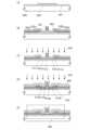
図1(A)乃至図1(D)にトランジスタ及びトランジスタの作製方法の一例を示す。Figures 1(A) to 1(D) show an example of a transistor and a method for manufacturing the transistor.
図1(D)に示すトランジスタ410は、トップゲート構造の薄膜トランジスタの一つで
あり、プレーナ型薄膜トランジスタともいう。A
トランジスタ410は、絶縁表面を有する基板400上に、絶縁層407と、チャネル形
成領域413、酸素欠陥誘起因子を含むソース領域414a、及び酸素欠陥誘起因子を含
むドレイン領域414bが設けられている酸化物半導体層403と、ゲート絶縁層402
と、ゲート電極層401と、を有する。The
and a
酸化物半導体層403、ゲート絶縁層402、及びゲート電極層401を覆い、絶縁層4
09及び絶縁層411が積層されており、絶縁層409及び絶縁層411を介して、ソー
ス領域414a、及びドレイン領域414bにそれぞれソース電極層405a、ドレイン
電極層405bが電気的に接続して設けられている。The
A
ソース領域414a、及びドレイン領域414bは、酸素欠陥誘起因子の導入によってド
ナーが形成された低抵抗化領域である。The
以下、図1(A)乃至(D)を用い、基板400上にトランジスタ410を作製する工程
を説明する。A process for manufacturing a
絶縁表面を有する基板400に使用することができる基板に大きな制限はないが、少なく
とも、後の加熱処理に耐えうる程度の耐熱性を有していることが必要となる。There is no particular limitation on the substrate that can be used for the
例えば、基板として、ガラス基板を用いる場合、後の加熱処理の温度が高い場合には、歪
み点が730℃以上のものを用いると良い。ガラス基板には、例えば、アルミノシリケー
トガラス、アルミノホウケイ酸ガラス、バリウムホウケイ酸ガラスなどのガラス材料が用
いられている。なお、実用的な耐熱ガラスである、酸化ホウ素(B2O3)より酸化バリ
ウム(BaO)を多く含むガラス基板を用いてもよい。For example, when a glass substrate is used as the substrate, if the temperature of the subsequent heat treatment is high, it is preferable to use a substrate having a distortion point of 730° C. or higher. For the glass substrate, for example, a glass material such as aluminosilicate glass, aluminoborosilicate glass, or barium borosilicate glass is used. Note that a glass substrate containing more barium oxide (BaO) than boron oxide (BO), which is a practical heat-resistant glass, may be used.
なお、上記のガラス基板に代えて、セラミック基板、石英基板、サファイア基板などの絶
縁体でなる基板を用いても良い。他にも、結晶化ガラスなどを用いることができる。また
、プラスチック基板等も適宜用いることができる。Instead of the glass substrate, a substrate made of an insulating material such as a ceramic substrate, a quartz substrate, or a sapphire substrate may be used. In addition, crystallized glass may be used. Furthermore, a plastic substrate may be used as appropriate.
下地膜となる絶縁層407を基板400上に形成する。絶縁層407は、基板400から
の不純物元素の拡散を防止する機能があり、窒化シリコン層、酸化シリコン層、窒化酸化
シリコン層、酸化窒化シリコン層、窒化アルミニウム層、酸化アルミニウム層、窒化酸化
アルミニウム層、又は酸化窒化アルミニウム層から選ばれた一又は複数の膜による積層構
造により形成することができる。絶縁層407の形成方法としては、プラズマCVD法又
はスパッタリング法等を用いることができる。例えば、絶縁層407として、酸化シリコ
ン層をスパッタリング法で形成することができる。An insulating
絶縁層407上に酸化物半導体膜を形成する。An oxide semiconductor film is formed on the insulating
酸化物半導体膜に用いる酸化物半導体としては、四元系金属の酸化物であるIn-Sn-
Ga-Zn-O系や、三元系金属の酸化物であるIn-Ga-Zn-O系、In-Sn-
Zn-O系、In-Al-Zn-O系、Sn-Ga-Zn-O系、Al-Ga-Zn-O
系、Sn-Al-Zn-O系や、二元系金属の酸化物であるIn-Zn-O系、Sn-Z
n-O系、Al-Zn-O系、Zn-Mg-O系、Sn-Mg-O系、In-Mg-O系
や、In-O系、Sn-O系、Zn-O系などを用いることができる。ここで、例えば、
In-Ga-Zn-O系酸化物半導体とは、少なくともInとGaとZnを含む酸化物で
あり、その組成比に特に制限はない。また、InとGaとZn以外の元素を含んでもよい
。また、上記酸化物半導体膜にSiO2を含んでもよい。The oxide semiconductor used for the oxide semiconductor film is an oxide of a quaternary metal, In—Sn—
Ga-Zn-O system, In-Ga-Zn-O system which is an oxide of a ternary metal, In-Sn-
Zn—O system, In—Al—Zn—O system, Sn—Ga—Zn—O system, Al—Ga—Zn—O
Sn-Al-Zn-O system, In-Zn-O system which is an oxide of binary metals, Sn-Z
Examples of materials that can be used include n-O-based, Al-Zn-O-based, Zn-Mg-O-based, Sn-Mg-O-based, In-Mg-O-based, In-O-based, Sn-O-based, and Zn-O-based materials.
The In-Ga-Zn-O-based oxide semiconductor is an oxide containing at least In, Ga, and Zn, and there is no particular limitation on the composition ratio. In addition, elements other than In, Ga, and Zn may be contained. In addition, the oxide semiconductor film may contain SiO2.
また、酸化物半導体膜は、化学式InMO3(ZnO)m(m>0)で表記される酸化物
半導体を用いることができる。ここで、Mは、Ga、Al、MnおよびCoから選ばれた
一または複数の金属元素を示す。例えばMとして、Ga、Ga及びAl、Ga及びMn、
またはGa及びCoなどがある。For the oxide semiconductor film, an oxide semiconductor represented by the chemical formula InMO3(ZnO)m (m>0) can be used, where M represents one or more metal elements selected from Ga, Al, Mn, and Co. For example, M can be Ga, Ga and Al, Ga and Mn,
Or Ga and Co.
酸化物半導体膜はスパッタリング法によって形成することができる。本実施の形態では、
In-Ga-Zn-O系酸化物ターゲットを用いてスパッタリング法により酸化物半導体
膜を成膜し、島状に加工して酸化物半導体層420を形成する(図1(A)参照)。The oxide semiconductor film can be formed by a sputtering method.
An oxide semiconductor film is formed by a sputtering method using an In--Ga--Zn--O-based oxide target and processed into an island shape to form an oxide semiconductor layer 420 (see FIG. 1A).
酸化物半導体層420上にゲート絶縁層402を形成する。ゲート絶縁層402は、プラ
ズマCVD法又はスパッタリング法等を用いて、酸化シリコン層、窒化シリコン層、酸化
窒化シリコン層、窒化酸化シリコン層、酸化アルミニウム層、窒化アルミニウム層、酸化
窒化アルミニウム層、窒化酸化アルミニウム層、又は酸化ハフニウム層を単層又は積層し
て形成することができる。例えば、スパッタリング法を用いて膜厚100nmの酸化シリ
コン層を形成し、ゲート絶縁層402とすればよい。A
ゲート絶縁層402は、酸化物半導体層420側から酸化シリコン層と窒化シリコン層を
積層した構造とすることもできる。例えば、第1のゲート絶縁層としてスパッタリング法
により膜厚5nm以上300nm以下の酸化シリコン層(SiOx(x>0))を形成し
、第1のゲート絶縁層上に第2のゲート絶縁層として膜厚50nm以上200nm以下の
窒化シリコン層(SiNy(y>0))を積層してもよい。ゲート絶縁層402の膜厚は
、薄膜トランジスタに要求される特性によって適宜設定すればよく30nm乃至400n
m程度でもよい。The
It may be about m.
ゲート絶縁層402上にゲート電極層401を形成する(図1(B)参照)。ゲート電極
層401の材料は、モリブデン、チタン、クロム、タンタル、タングステン、アルミニウ
ム、銅、ネオジム、スカンジウム等の金属材料またはこれらを主成分とする合金材料を用
いて、単層でまたは積層して形成することができる。A
例えば、ゲート電極層401の2層の積層構造としては、アルミニウム層上にモリブデン
層が積層された2層の積層構造、または銅層上にモリブデン層を積層した2層構造、また
は銅層上に窒化チタン層若しくは窒化タンタルを積層した2層構造、窒化チタン層とモリ
ブデン層とを積層した2層構造とすることが好ましい。3層の積層構造としては、タング
ステン層または窒化タングステン層と、アルミニウムとシリコンの合金またはアルミニウ
ムとチタンの合金と、窒化チタン層またはチタン層とを積層した構造とすることが好まし
い。なお、透光性を有する導電膜を用いてゲート電極層を形成することもできる。透光性
を有する導電膜としては、透光性導電性酸化物等をその例に挙げることができる。For example, the two-layer stack structure of the
次に、酸化物半導体層420に酸素欠陥誘起因子421を導入し、ソース領域414a、
ドレイン領域414b、チャネル形成領域413を含む酸化物半導体層403を形成する
(図1(C)参照)。例えば、ソース領域414a、ドレイン領域414bに含まれる酸
素欠陥誘起因子421の濃度は、1×10¹⁹atoms/cm3以上1×1021at
oms/cm3以下とすればよい。Next, an oxygen
An
It is sufficient to set it to oms/cm3 or less.
酸素欠陥誘起因子421の導入処理の後に加熱処理(例えば200℃以上600℃以下)
を行っても良い。After the introduction of the oxygen
may also be carried out.
本明細書において、酸素欠陥誘起因子の濃度とは、酸化物半導体層の成膜後、導入処理に
よって導入された酸素欠陥誘起因子の濃度であり、成膜時など導入処理以外の工程で含ま
れた酸素欠陥誘起因子と同じ元素は考慮しないものとする。In this specification, the concentration of the oxygen-defect-inducing factor refers to the concentration of the oxygen-defect-inducing factor introduced by an introduction treatment after the formation of the oxide semiconductor layer, and does not take into account elements that are the same as the oxygen-defect-inducing factor and that are contained in a process other than the introduction treatment, such as during the film formation.
酸素欠陥誘起因子421としては、チタン(Ti)、タングステン(W)、モリブデン(
Mo)、アルミニウム(Al)、コバルト(Co)、亜鉛(Zn)、インジウム(In)
、シリコン(Si)、ボロン(B)のいずれか一または複数から選択された元素を用いる
ことができる。さらに、上記酸素欠陥誘起因子に加えて、水素、又は\及び窒素を用いて
もよい。The oxygen
Mo), aluminum (Al), cobalt (Co), zinc (Zn), indium (In)
In addition to the oxygen vacancy inducing factors, hydrogen and/or nitrogen may be used.
酸化物半導体層420に、選択的に酸素欠陥誘起因子421を導入することによって、該
導入領域において酸素欠陥を効果的に誘起する。酸素欠陥はドナーとして機能するため、
選択的に低抵抗化したソース領域414a及びドレイン領域414bを有する酸化物半導
体層403を形成することができる。By selectively introducing the oxygen
The
本実施の形態では、酸素欠陥誘起因子421の導入処理において、ゲート電極層401を
マスクとして用いる。よって、酸化物半導体層403において、自己整合的に、ゲート電
極層401と重なる領域は、酸素欠陥誘起因子421が導入されずチャネル形成領域41
3となり、一方ゲート電極層401と重ならない領域には、酸素欠陥誘起因子421が導
入されソース領域414a、ドレイン領域414bが形成される。また、酸化物半導体層
420の少なくともチャネル形成領域上を覆うマスクを別途設けて、酸素欠陥誘起因子4
21の導入処理を行ってもよい。該マスクとしては、フォトリソグラフィ工程によるレジ
ストマスクを用いればよい。In this embodiment, the
On the other hand, in a region that does not overlap with the
The introduction process of 21 may be performed using a resist mask formed by a photolithography process as the mask.
酸化物半導体層中に酸素欠陥を形成することによる低抵抗化の効果を計算機を用いた計算
結果に基づいて検証した。酸化物半導体層として、In-Ga-Zn-O系の酸化物半導
体材料を用いる場合について計算を行っている。なお、計算において、In-Ga-Zn
-O系の酸化物半導体材料の組成はIn:Ga:Zn:O=1:1:1:4とした。The effect of reducing the resistance by forming oxygen defects in an oxide semiconductor layer was verified based on the results of calculations using a computer. The calculations were performed for the case where an In—Ga—Zn—O-based oxide semiconductor material was used for the oxide semiconductor layer.
The composition of the —O-based oxide semiconductor material was In:Ga:Zn:O=1:1:1:4.
まず、古典MD(分子動力学)計算を用いたmelt-quench法により、In-G
a-Zn-O系酸化物半導体の非晶質構造を用意した。ここでは、総原子数が84個、密
度が5.9g/cm3の構造について計算を行っている。金属-酸素間および酸素-酸素
間についてはBorn-Mayer-Huggins型のポテンシャルを、金属-金属間
についてはLennard-Jones型のポテンシャルを用い、NVTアンサンブルで
計算を行った。計算プログラムとしては、Materials Explorerを用い
た。First, the melt-quench method using classical MD (molecular dynamics) calculations was used to calculate the In-G
An amorphous structure of a-Zn-O-based oxide semiconductor was prepared. Here, calculations were performed for a structure with a total number of atoms of 84 and a density of 5.9 g/cm3. A Born-Mayer-Huggins potential was used for metal-oxygen and oxygen-oxygen, and a Lennard-Jones potential was used for metal-metal, and calculations were performed with an NVT ensemble. Materials Explorer was used as the calculation program.
その後、上記古典MD計算により得られた構造に対して、密度汎関数理論(DFT)に基
づく平面波-擬ポテンシャル法を用いた第一原理計算(量子MD計算)により、構造を最
適化し、状態密度を求めた。また、任意の酸素原子を一つ取り除いた構造に対しても構造
最適化を行い、状態密度を計算した。計算プログラムとしてはCASTEPを、交換相関
汎関数としてはGGA-PBEを用いた。After that, the structure obtained by the classical MD calculation was optimized by first-principles calculation (quantum MD calculation) using a plane wave-pseudopotential method based on density functional theory (DFT) to obtain the density of states. In addition, the structure was optimized for a structure in which one arbitrary oxygen atom was removed, and the density of states was calculated. CASTEP was used as the calculation program, and GGA-PBE was used as the exchange-correlation functional.
図8に、上記計算結果により得られた構造の状態密度を示す。図8(A)は、酸素欠陥の
ない構造の状態密度であり、図8(B)は、酸素欠陥がある構造の状態密度である。ここ
で、0(eV)はフェルミ準位に対応するエネルギーを表している。図8(A)および図
8(B)より、酸素欠陥がない構造では、フェルミ準位は価電子帯の上端に存在するのに
対して、酸素欠陥がある構造では、フェルミ準位は伝導帯中に存在することが分かる。酸
素欠陥がある構造ではフェルミ準位が伝導帯中に存在するため、伝導に寄与する電子数が
増加し、抵抗が低い(導電率の高い)構造が得られる。FIG. 8 shows the density of states of the structure obtained by the above calculation results. FIG. 8(A) shows the density of states of a structure without oxygen defects, and FIG. 8(B) shows the density of states of a structure with oxygen defects. Here, 0 (eV) represents the energy corresponding to the Fermi level. From FIG. 8(A) and FIG. 8(B), it can be seen that in a structure without oxygen defects, the Fermi level exists at the top of the valence band, whereas in a structure with oxygen defects, the Fermi level exists in the conduction band. In a structure with oxygen defects, the Fermi level exists in the conduction band, so the number of electrons contributing to conduction increases, resulting in a structure with low resistance (high conductivity).
よって、酸化物半導体層に、選択的に酸素欠陥誘起因子を導入し酸素欠陥を効果的に誘起
することによって、酸化物半導体層に低抵抗化したソース領域及びドレイン領域を形成す
ることができる。Therefore, by selectively introducing an oxygen defect inducing factor into the oxide semiconductor layer to effectively induce oxygen defects, a source region and a drain region with low resistance can be formed in the oxide semiconductor layer.
なお、酸素欠陥誘起因子421としては、酸素親和性の高い金属元素を用いるとより好ま
しい。酸素親和性の高い金属元素としては、例えば、チタン、アルミニウム、マンガン、
マグネシウム、ジルコニウム、ベリリウムなどが挙げられる。また、銅などを用いても良
い。It is more preferable to use a metal element having a high oxygen affinity as the oxygen
Examples of the metal include magnesium, zirconium, and beryllium. Copper may also be used.
次に、酸素親和性の高い金属元素を酸素欠陥誘起因子として用いる場合の効果について、
計算機を用いた計算結果に基づいて説明する。ここでは、酸素親和性の高い金属元素とし
てチタンを用い、酸化物半導体層として、In-Ga-Zn-O系の酸化物半導体材料を
用いる場合について計算を行っているが、開示する発明の一態様はこれに限定されない。
なお、計算において、In-Ga-Zn-O系の酸化物半導体材料の組成はIn:Ga:
Zn:O=1:1:1:4とした。Next, the effect of using metal elements with high oxygen affinity as oxygen vacancy inducers will be discussed.
The following description will be based on the results of calculations using a computer. Here, the calculations are performed for the case where titanium is used as a metal element having high oxygen affinity and an In—Ga—Zn—O-based oxide semiconductor material is used for the oxide semiconductor layer; however, one embodiment of the disclosed invention is not limited thereto.
In the calculation, the composition of the In—Ga—Zn—O-based oxide semiconductor material was In:Ga:
The Zn:O ratio was 1:1:1:4.
酸素親和性の高い金属元素を導入することにより、非晶質状態の酸化物半導体から酸素親
和性の高い金属元素へと酸素が移動する様子を確認した。By introducing a metal element with high oxygen affinity, it was confirmed that oxygen moves from the amorphous oxide semiconductor to the metal element with high oxygen affinity.
酸化物半導体として、In-Ga-Zn-O系酸化物半導体にチタン(Ti)を含ませた
構造の電子状態について計算を行った。計算モデル及び計算条件を以下に示す。The electronic state of an oxide semiconductor having a structure in which titanium (Ti) is contained in an In-Ga-Zn-O-based oxide semiconductor was calculated. The calculation model and calculation conditions are shown below.
計算に用いたTiを含むIn-Ga-Zn-O系酸化物半導体の構造を図9に示す。この
構造は、第一原理分子動力学計算により作製した化学量論的組成のIn-Ga-Zn-O
系酸化物半導体にTiを含ませた構造である。黒丸が金属原子、白丸が酸素原子を表す。
大きな黒丸がTiである。原子数は、図9のTiを含むIn-Ga-Zn-O系酸化物半
導体構造において、In、Ga、Znがそれぞれ12個、Oが48個、Tiが1個である
。The structure of the In-Ga-Zn-O oxide semiconductor containing Ti used in the calculation is shown in Figure 9. This structure is an In-Ga-Zn-O oxide semiconductor with a stoichiometric composition created by first-principles molecular dynamics calculation.
The black circles represent metal atoms and the white circles represent oxygen atoms.
The large black circles represent Ti. The number of atoms is 12 each for In, Ga, and Zn, 48 for O, and 1 for Ti in the In-Ga-Zn-O-based oxide semiconductor structure including Ti in FIG.
Tiを含むIn-Ga-Zn-O系酸化物半導体構造の密度は、非晶質In-Ga-Zn
-O系酸化物半導体の実験値5.9g/cm3に固定した。この構造に対して、下記計算
条件で計算を行った。第一原理計算はaccelrys社製の第一原理計算ソフトCAS
TEPを用いた。The density of the In—Ga—Zn—O-based oxide semiconductor structure containing Ti is
The experimental value for the -O-based oxide semiconductor was fixed at 5.9 g/cm3. Calculations were performed for this structure under the following calculation conditions. The first-principles calculations were performed using the first-principles calculation software CAS manufactured by Accelrys.
TEP was used.
図9のTiを含むIn-Ga-Zn-O系酸化物半導体構造は、温度3000Kより、1
500K、300Kと温度を降温させながら、粒子数(N)、体積(V)、温度(T)が
一定の条件(NVTアンサンブル)で、時間刻み幅1fsec、ステップ数は各温度で2
000step、電子のカットオフエネルギー260eV、逆格子のメッシュ(k点)を
1×1×1にして計算し、その最終構造に対して、さらに電子のカットオフエネルギー4
20eV、逆格子のメッシュ(k点)を2×2×2にして構造最適化計算を行い、エネル
ギーの低い安定構造としたものである。The Ti-containing In-Ga-Zn-O-based oxide semiconductor structure shown in FIG.
The temperature was lowered from 500K to 300K, and the number of particles (N), volume (V), and temperature (T) were kept constant (NVT ensemble). The time step width was 1 fsec, and the number of steps was 2 at each temperature.
000 steps, electron cutoff energy 260 eV, reciprocal lattice mesh (k point) 1x1x1, and the calculation is performed. For the final structure, the electron cutoff energy is further increased to 4
A structural optimization calculation was performed at 20 eV with a reciprocal lattice mesh (k-point) of 2×2×2 to obtain a stable structure with low energy.
図9に示すように、チタンは酸素と結合している。Titanium is bonded to oxygen, as shown in Figure 9.
図9のTiを含むIn-Ga-Zn-O系酸化物半導体構造に対して、電子のカットオフ
エネルギー420eV、逆格子のメッシュ(k点)が3×3×3の条件で、電子の状態密
度を計算した。For the Ti-containing In--Ga--Zn--O-based oxide semiconductor structure of FIG. 9, the electron density of states was calculated under the conditions of an electron cutoff energy of 420 eV and a reciprocal lattice mesh (k-point) of 3×3×3.
図10(A)にIn-Ga-Zn-O系酸化物半導体構造における全体の状態密度、図1
0(B)にTiを含むIn-Ga-Zn-O系酸化物半導体構造のTiの部分状態密度を
示す。図10(A)(B)において、横軸はエネルギー、縦軸は状態密度を表す。横軸の
エネルギーの原点は電子の最大占有準位のエネルギーを表す。図10(B)に示すように
、In-Ga-Zn-O系酸化物半導体にTiを添加すると伝導帯下端に電子が入ること
がわかる。FIG. 10A shows the overall density of states in an In—Ga—Zn—O-based oxide semiconductor structure.
10A and 10B show partial densities of states of Ti in an In-Ga-Zn-O-based oxide semiconductor structure containing Ti. In Figures 10A and 10B, the horizontal axis represents energy, and the vertical axis represents density of states. The origin of the energy on the horizontal axis represents the energy of the maximum occupied level of electrons. As shown in Figure 10B, it can be seen that when Ti is added to an In-Ga-Zn-O-based oxide semiconductor, electrons enter the bottom of the conduction band.
上記の結果から、TiがIn-Ga-Zn-O系酸化物半導体中に導入されると、それら
と酸素が結合する事により、化学量論比からずれる。それによって、酸素が欠乏状態とな
る。非晶質In-Ga-Zn-O系酸化物半導体では、酸素欠損は電子ドナーとなるので
、結果として電子が過剰の状態になる。よって、酸素と結合しやすいTiを導入した場合
には酸素欠陥を引き起こし、キャリアが発生する。From the above results, when Ti is introduced into an In-Ga-Zn-O-based oxide semiconductor, it bonds with oxygen, causing deviation from the stoichiometric ratio. This causes an oxygen deficiency. In an amorphous In-Ga-Zn-O-based oxide semiconductor, oxygen vacancies act as electron donors, resulting in an excess of electrons. Therefore, when Ti, which easily bonds with oxygen, is introduced, oxygen vacancies are caused, and carriers are generated.
このように、酸化物半導体層に酸素親和性の高い金属元素を導入することにより、その導
入領域において、酸化物半導体層から金属元素へと酸素原子が移動し、酸素欠陥がより効
果的に増加することが確認できる。結果、ドナーとして機能する酸素欠陥の増加により、
導入領域はより効率的に低抵抗化する。In this way, it can be confirmed that by introducing a metal element having a high oxygen affinity into the oxide semiconductor layer, oxygen atoms move from the oxide semiconductor layer to the metal element in the introduced region, and oxygen defects are more effectively increased. As a result, the increase in oxygen defects functioning as donors leads to
The introduction region becomes more efficiently low resistance.
酸素欠陥誘起因子の導入により低抵抗化されたソース領域及びドレイン領域を有すること
で、酸化物半導体を有するトランジスタにおいては、酸化物半導体層と電極層とのコンタ
クト抵抗が低減できるため、オン特性(例えば、オン電流や電界効果移動度)が向上する
。よって、電気特性が高いトランジスタとすることが可能となる。By providing the source and drain regions with reduced resistance by introducing oxygen vacancy-inducing factors, the contact resistance between the oxide semiconductor layer and the electrode layer in a transistor having an oxide semiconductor can be reduced, and thus the on-characteristics (for example, on-current and field-effect mobility) can be improved. Thus, the transistor can have excellent electrical characteristics.
酸化物半導体層420への酸素欠陥誘起因子421の導入処理は、成膜された酸化物半導
体層420へ選択的にイオン注入法やドーピング法を用いて行う。本実施の形態では酸素
欠陥誘起因子421としてチタンを用いて、イオン注入法により酸化物半導体層420へ
導入する。イオン注入法としては、四塩化チタン(TiCl4)液化ガスを用いる方法や
、固体ソースを蒸気化する方法等がある。The oxygen-
なお、酸素欠陥誘起因子導入処理において、導入条件(加速エネルギー、酸素欠陥誘起因
子の照射量(注入量又はドーズ量))によっては、マスク(本実施の形態ではゲート電極
層401)と重なる領域であっても、酸化物半導体層の一部に酸素欠陥誘起因子が含まれ
ることがある。よって、酸素欠陥誘起因子を導入する領域は、導入条件やマスクの膜厚や
大きさを適宜設定することによって制御することができる。Note that in the oxygen-defect-inducing factor introduction process, the oxygen-defect-inducing factor may be contained in a part of the oxide semiconductor layer even in a region overlapping with a mask (the
例えば、酸化物半導体層への酸素欠陥誘起因子の導入処理における、導入条件についてT
RIM(Transport of Ion in Matter)と呼ばれるソフトを
用いて計算を行った。TRIMはモンテカルロ法によってイオン注入過程の計算を行うた
めのソフトである。計算に用いたモデルは、絶縁層407として酸化シリコン膜、酸化物
半導体層420として非晶質のIn-Ga-Zn-O膜(組成:InGaZnO4、密度
6.2g/cm3、膜厚50nm)、ゲート絶縁層402として酸化シリコン膜(密度2
.2g/cm3、膜厚100nm)の積層であり、酸化物半導体層420に、ゲート絶縁
層402を通過して酸素欠陥誘起因子421を導入した。酸素欠陥誘起因子421として
はチタンイオン(Ti+)を用い、ドーズ量1×1015cm-2でイオン注入法により
導入した。また加速エネルギーは100keV、150keV、200keVの3条件に
おいて計算した。For example, the introduction conditions in the process of introducing oxygen defect inducing factors into the oxide semiconductor layer are T
The calculation was performed using software called Transport of Ion in Matter (RIM). TRIM is software for calculating the ion implantation process by the Monte Carlo method. The model used for the calculation was a silicon oxide film as the insulating
The
計算による酸素欠陥誘起因子の導入深さと濃度の関係を図7に示す。図7において横軸は
酸化物半導体層420表面からの酸素欠陥誘起因子の導入深さ(nm)、縦軸は導入され
た酸素欠陥誘起因子の濃度(atoms/cm3)である。図7に示すように加速エネル
ギーは100keV、150keV、200keVの3条件ともに、酸化物半導体層42
0中に酸素欠陥誘起因子であるチタンイオンが1×10²⁰atoms/cm3程度導入
されていることが確認できる。The calculated relationship between the introduction depth and the concentration of the oxygen defect inducing factor is shown in FIG. 7. In FIG. 7, the horizontal axis represents the introduction depth (nm) of the oxygen defect inducing factor from the surface of the
It can be seen that titanium ions, which are oxygen vacancy inducing factors, are introduced into SiO2 at about 1×10²⁰ atoms/cm3.
従って、上記計算モデルにおいて酸化物半導体層に濃度1×10¹⁹atoms/cm3
以上1×10²¹atoms/cm3以下のソース領域及びドレイン領域を形成するため
のチタンイオンの導入条件は、ドーズ量1×1014cm-2以上1×1016cm-2
以下、加速エネルギー100keV以上200keV以下とすればよい。Therefore, in the above calculation model, the oxide semiconductor layer has a concentration of 1×10¹⁹ atoms/cm3
The conditions for introducing titanium ions to form the source and drain regions are a dose of 1×1014 cm-2 to 1×1016 cm-2.
Hereinafter, the acceleration energy may be set to 100 keV or more and 200 keV or less.
酸化物半導体層403のチャネル形成領域413にも酸素欠陥誘起因子を導入してもよい
。この場合は、ゲート電極層401の形成前に酸化物半導体層420に酸素欠陥誘起因子
の導入処理を行う。酸素欠陥誘起因子の導入処理は酸化物半導体膜を島状に加工する前に
行ってもよい。チャネル形成領域413にも酸素欠陥誘起因子を導入し、酸素欠陥をドナ
ーとして低抵抗化(例えばn--型化)させることで、トランジスタの電気特性をより制
御することができる。An oxygen-defect-inducing factor may also be introduced into a
酸素欠陥誘起因子の導入処理の後に加熱処理(例えば200℃以上600℃以下)を行っ
ても良い。After the treatment for introducing the oxygen defect inducing factor, a heat treatment (for example, at 200° C. or higher and 600° C. or lower) may be performed.
チャネル形成領域413に含まれる酸素欠陥誘起因子の濃度は、ソース領域414a及び
ドレイン領域414bより低濃度とする。本実施の形態のようにソース領域414a及び
ドレイン領域414bに含まれる酸素欠陥誘起因子の濃度が1×10¹⁹atoms/c
m3以上1×10²¹atoms/cm3以下であれば、例えば、チャネル形成領域41
3の濃度は1×10¹⁴atoms/cm3未満とすればよい。The concentration of the oxygen defect inducing factor contained in the
If the concentration is 1×10 atoms/cm or more, for example, the channel formation region 41
The concentration of 3 may be less than 1×10 14 atoms/
次いで、酸化物半導体層403、ゲート絶縁層402、ゲート電極層401を覆う絶縁層
409と絶縁層411を積層する。Next, an insulating
絶縁層409と絶縁層411としては、酸化絶縁層、又は窒化絶縁層などの無機絶縁膜を
好適に用いることができる。また、絶縁層409、絶縁層411の作製方法としては、プ
ラズマCVD法又はスパッタリング法等を用いればよい。An inorganic insulating film such as an oxide insulating layer or a nitride insulating layer can be preferably used for the insulating
絶縁層409は、代表的には酸化シリコン膜、酸化窒化シリコン膜、酸化アルミニウム膜
、または酸化窒化アルミニウム膜などの無機絶縁膜を用いることができる。The insulating
絶縁層411は、窒化シリコン膜、窒化アルミニウム膜、窒化酸化シリコン膜、窒化酸化
アルミニウム膜などの無機絶縁膜を用いることができる。The insulating
また、絶縁層411上にトランジスタ起因の表面凹凸を低減するために平坦化絶縁膜を形
成してもよい。平坦化絶縁膜としては、ポリイミド、アクリル、ベンゾシクロブテン、ポ
リアミド、エポキシ等の、耐熱性を有する有機材料を用いることができる。また上記有機
材料の他に、低誘電率材料(low-k材料)、シロキサン系樹脂、PSG(リンガラス
)、BPSG(リンボロンガラス)等を用いることができる。なお、これらの材料で形成
される絶縁膜を複数積層させることで、平坦化絶縁膜を形成してもよい。平坦化絶縁膜の
形成法は、特に限定されず、その材料に応じて、スパッタリング法、SOG法、スピンコ
ート、ディップ、スプレー塗布、液滴吐出法(インクジェット法、スクリーン印刷、オフ
セット印刷等)、ドクターナイフ、ロールコーター、カーテンコーター、ナイフコーター
等を用いることができる。A planarizing insulating film may be formed on the insulating
絶縁層409と絶縁層411にソース領域414a、ドレイン領域414bに達する開口
(コンタクトホール)を形成する。開口に導電膜を成膜し、エッチングにより加工してソ
ース領域414a、ドレイン領域414bと接し、電気的に接続するソース電極層405
a、ドレイン電極層405bを形成する(図1(D)参照)。以上の工程でトランジスタ
410を作製することができる。Openings (contact holes) reaching the
Through the above steps, a
ソース電極層405a、ドレイン電極層405bに用いる導電膜としては、例えば、Al
、Cr、Cu、Ta、Ti、Mo、Wからから選ばれた元素、または上述した元素を成分
とする合金か、上述した元素を組み合わせた合金膜等を用いることができる。また、Al
、Cuなどの金属層の下側又は上側の一方または双方にCr、Ta、Ti、Mo、Wなど
の高融点金属層を積層させた構成としても良い。また、Si、Ti、Ta、W、Mo、C
r、Nd、Sc、YなどAl膜に生ずるヒロックやウィスカーの発生を防止する元素が添
加されているAl材料を用いることで耐熱性を向上させることが可能となる。また、窒化
チタンなどの上記金属の導電性窒化物材料を用いてもよい。また、導電膜の作製方法とし
ては、蒸着法又はスパッタリング法等を用いればよい。The conductive film used for the
, Cr, Cu, Ta, Ti, Mo, and W, or an alloy containing the above elements, or an alloy film containing a combination of the above elements, etc. can be used.
A high melting point metal layer such as Cr, Ta, Ti, Mo, or W may be laminated on either or both of the upper and lower sides of a metal layer such as Si, Ti, Ta, W, Mo, or C.
It is possible to improve heat resistance by using an Al material to which elements such as r, Nd, Sc, and Y that prevent the generation of hillocks and whiskers in the Al film are added. Conductive nitride materials of the above metals such as titanium nitride may also be used. The conductive film may be formed by deposition, sputtering, or the like.
また、ソース電極層405a、ドレイン電極層405bは、単層構造でも、2層以上の積
層構造としてもよい。例えば、シリコンを含むアルミニウム膜の単層構造、アルミニウム
膜上にチタン膜を積層する2層構造、Ti膜と、そのTi膜上に重ねてアルミニウム膜を
積層し、さらにその上にTi膜を成膜する3層構造などが挙げられる。The
また、ソース電極層405a、ドレイン電極層405b(これと同じ層で形成される配線
層を含む)となる導電膜としては導電性の金属酸化物で形成しても良い。導電性の金属酸
化物としては酸化インジウム(In2O3)、酸化スズ(SnO2)、酸化亜鉛(ZnO
)、酸化インジウム酸化スズ合金(In2O3―SnO2、ITOと略記する)、酸化イ
ンジウム酸化亜鉛合金(In2O3―ZnO)または前記金属酸化物材料にシリコン若し
くは酸化シリコンを含ませたものを用いることができる。The conductive film to be the
), an indium oxide tin oxide alloy (In2O3-SnO2, abbreviated as ITO), an indium oxide zinc oxide alloy (In2O3-ZnO), or a material obtained by adding silicon or silicon oxide to the above metal oxide material can be used.
以上のように、酸素欠陥誘起因子の導入により低抵抗化されたソース領域414a及びド
レイン領域414bを有する酸化物半導体を有するトランジスタ410は、酸化物半導体
層403とソース電極層405a、ドレイン電極層405bとのコンタクト抵抗が低減で
きるため、オン特性が向上する。よって、電気特性が高いトランジスタとすることが可能
となる。As described above, the
電気特性が高いトランジスタは、高速応答及び高速駆動が可能なため、該トランジスタを
有することで高機能な半導体装置とすることができる。A transistor with excellent electrical characteristics can respond quickly and be driven at high speed; therefore, including such a transistor can provide a high-performance semiconductor device.
(実施の形態2)
本実施の形態では、半導体装置及び半導体装置の作製方法の一形態を図2及び図3を用い
て説明する。本実施の形態では、半導体装置の一例としてトランジスタを示す。実施の形
態1に示すトランジスタにおいて、チャネル形成領域とソース領域又はドレイン領域の間
に、ソース領域及びドレイン領域より低濃度の酸素欠陥誘起因子を含む領域を有する構造
である。よって、上記実施の形態と同一部分又は同様な機能を有する部分、及び工程は、
上記実施の形態と同様に行うことができ、繰り返しの説明は省略する。また同じ箇所の詳
細な説明は省略する。(Embodiment 2)
In this embodiment, one embodiment of a semiconductor device and a method for manufacturing the semiconductor device will be described with reference to FIGS. 2 and 3. In this embodiment, a transistor is shown as an example of a semiconductor device. The transistor shown in
This embodiment can be carried out in the same manner as the above embodiment, and therefore a repeated explanation will be omitted. Also, detailed explanation of the same parts will be omitted.
図2(A)乃至図2(D)及び図3(A)乃至図3(D)にトランジスタ及びトランジス
タの作製方法の一例を示す。2A to 2D and 3A to 3D illustrate examples of transistors and methods for manufacturing the transistors.
図2(D)に示すトランジスタ440は、トップゲート構造の薄膜トランジスタの一つで
あり、プレーナ型薄膜トランジスタともいう。A
トランジスタ440は、絶縁表面を有する基板400上に、絶縁層407、チャネル形成
領域413、低濃度酸素欠陥誘起因子含有領域415a、415b、酸素欠陥誘起因子を
含むソース領域414a、酸素欠陥誘起因子を含むドレイン領域414bが設けられてい
る酸化物半導体層433、ゲート絶縁層402、及びゲート電極層401を有する。The
酸化物半導体層433、ゲート絶縁層402、及びゲート電極層401を覆い、絶縁層4
09及び絶縁層411が積層されており、絶縁層409及び絶縁層411を介して、ソー
ス領域414a、及びドレイン領域414bにそれぞれソース電極層405a、ドレイン
電極層405bが電気的に接続して設けられている。The
A
低濃度酸素欠陥誘起因子含有領域415a、415b、ソース領域414a及びドレイン
領域414bは、酸素欠陥誘起因子を含む領域であり、低濃度酸素欠陥誘起因子含有領域
415a、415bより酸素欠陥誘起因子の濃度が高いソース領域414a、及びドレイ
ン領域414bは高濃度酸素欠陥誘起因子含有領域であるともいえる。よって、本明細書
においては、高濃度酸素欠陥誘起因子含有領域であるソース領域414a及びドレイン領
域414bを第1の領域、一方低濃度酸素欠陥誘起因子含有領域415a、415bを第
2の領域ともいう。The low-concentration oxygen-defect-inducing-factor-containing
低濃度酸素欠陥誘起因子含有領域415a、415b、ソース領域414a、及びドレイ
ン領域414bは、酸素欠陥誘起因子によってドナーが形成された低抵抗化領域である。
低濃度酸素欠陥誘起因子含有領域415a、415bは、高濃度酸素欠陥誘起因子含有領
域であるソース領域414a、及びドレイン領域414bより含有する酸素欠陥誘起因子
の濃度が低いため、ソース領域及びドレイン領域よりも抵抗が高い。The low concentration oxygen-defect-inducing
The low-concentration oxygen-defect-inducing-factor-containing
従って、トランジスタ440の酸化物半導体層433において、チャネル形成領域413
、低濃度酸素欠陥誘起因子含有領域415a及び415b、ソース領域414a及びドレ
イン領域414bの順に抵抗が低くなっている。Therefore, in the
The resistance decreases in the order of the low concentration oxygen defect inducing
以下、図2(A)乃至図2(D)を用い、基板400上にトランジスタ440を作製する
工程を説明する。A process for manufacturing a
実施の形態1の図1(B)に示すように絶縁層407が設けられた基板400上に島状の
酸化物半導体層420、ゲート絶縁層402、ゲート電極層401が形成されている(図
2(A)参照)。As shown in FIG. 1B in
酸化物半導体層420のチャネル形成領域に相当する領域(ゲート電極層401と重なる
領域)にも酸素欠陥誘起因子の導入処理を行い、酸素欠陥誘起因子を含ませてもよい。こ
の場合は、ゲート電極層401の形成前に酸化物半導体層420に酸素欠陥誘起因子の導
入処理を行う。酸素欠陥誘起因子の導入処理は酸化物半導体膜を島状に加工する前に行っ
てもよい。チャネル形成領域にも酸素欠陥誘起因子を導入し、酸素欠陥をドナーとして低
抵抗化(例えばn--型化)させることで、トランジスタの電気特性をより制御すること
ができる。An oxygen-defect-inducing factor may also be introduced into a region of the
酸素欠陥誘起因子の導入処理の後に加熱処理(例えば200℃以上600℃以下)を行っ
ても良い。After the treatment for introducing the oxygen defect inducing factor, a heat treatment (for example, at 200° C. or higher and 600° C. or lower) may be performed.
次いで、酸化物半導体層420、ゲート絶縁層402、ゲート電極層401を覆う絶縁層
409を形成する(図2(B)参照)。Next, an insulating
次に、酸化物半導体層420に酸素欠陥誘起因子434を導入し、低濃度酸素欠陥誘起因
子含有領域415a、415b、ソース領域414a、ドレイン領域414b、チャネル
形成領域413を含む酸化物半導体層433を形成する(図2(C)参照)。例えば、ソ
ース領域414a、ドレイン領域414bに含まれる酸素欠陥誘起因子434の濃度は、
1×10¹⁹atoms/cm3以上1×1021atoms/cm3以下とすればよい
。低濃度酸素欠陥誘起因子含有領域415a、415bはソース領域414a、ドレイン
領域414bより低い濃度とすればよく、例えば、低濃度酸素欠陥誘起因子含有領域41
5a、415bに含まれる酸素欠陥誘起因子434の濃度は、1×10¹⁸atoms/
cm3程度とすればよい。Next, an oxygen-defect-inducing
The low concentration oxygen vacancy inducing
The concentration of the
It is sufficient to set the volume to about cm3.
酸素欠陥誘起因子434の導入処理の後に加熱処理(例えば200℃以上600℃以下)
を行っても良い。After the introduction of the oxygen
may also be carried out.
酸素欠陥誘起因子434としては、チタン(Ti)、タングステン(W)、モリブデン(
Mo)、アルミニウム(Al)、コバルト(Co)、亜鉛(Zn)、インジウム(In)
、シリコン(Si)、ボロン(B)のいずれか一または複数から選択された元素を用いる
ことができる。さらに、上記酸素欠陥誘起因子に加えて、水素、又は\及び窒素を用いて
もよい。なお、酸素欠陥誘起因子434としては、酸素親和性の高い金属元素を用いると
より好ましい。The oxygen
Mo), aluminum (Al), cobalt (Co), zinc (Zn), indium (In)
The oxygen
酸化物半導体層420に、選択的に酸素欠陥誘起因子434を導入することによって、該
導入領域において酸素欠陥を効果的に誘起する。酸素欠陥はドナーとして機能するため、
選択的に低抵抗化した低濃度酸素欠陥誘起因子含有領域415a、415b、ソース領域
414a及びドレイン領域414bを有する酸化物半導体層433を形成することができ
る。By selectively introducing the oxygen
An
さらに、酸素欠陥誘起因子の導入領域に濃度分布を設け、高抵抗なチャネル形成領域と低
抵抗なソース領域又はドレイン領域の間に、ソース領域及びドレイン領域より高抵抗で、
かつチャネル形成領域より低抵抗な低濃度酸素欠陥誘起因子含有領域415a、415b
を有することによって、酸化物半導体層433は導電性を段階的に変化させた構造となる
。従って電界集中を抑制でき局所的な高電界の印加を防ぐため、トランジスタの耐圧が向
上し、半導体装置に高い信頼性を付与することができる。Furthermore, a concentration distribution is provided in the introduction region of the oxygen defect inducing factor, and a region having a higher resistance than the source region and drain region is provided between the high resistance channel formation region and the low resistance source region or drain region,
The low-concentration oxygen defect inducing factor-containing
Since the
本実施の形態では、酸素欠陥誘起因子434の導入処理において、ゲート電極層401を
マスクとして用いる。よって、酸化物半導体層433において、自己整合的に、ゲート電
極層401と重なる領域は、酸素欠陥誘起因子434が導入されずチャネル形成領域41
3となり、一方ゲート電極層401と重ならない領域には、酸素欠陥誘起因子434が導
入されソース領域414a、ドレイン領域414bが形成される。また、ゲート電極層4
01の側面に設けられた絶縁層409もマスクとなるので、ゲート電極層401及び側面
に設けられた絶縁層409と重なる酸化物半導体層420への導入は阻害される。但し、
ゲート電極層401の側面に設けられた絶縁層409と重なる酸化物半導体層420の領
域(チャネル形成領域413と、ソース領域414a又はドレイン領域414bの間)に
はソース領域又はドレイン領域へ導入された酸素欠陥誘起因子434の回り込みによって
酸素欠陥誘起因子434が導入されるので、低濃度酸素欠陥誘起因子含有領域415a、
415bとなる。In this embodiment, the
On the other hand, in the region not overlapping with the
Since the insulating
In a region of the
The result is 415b.
酸化物半導体層420への酸素欠陥誘起因子434の導入は、成膜された酸化物半導体層
420へ選択的にイオン注入法やドーピング法を用いて行う。The oxygen-defect-inducing
なお、酸素欠陥誘起因子導入処理において、導入条件(加速エネルギー、酸素欠陥誘起因
子の照射量(注入量又はドーズ量))によっては、マスク(本実施の形態ではゲート電極
層401)と重なる領域であっても、酸化物半導体層の一部に酸素欠陥誘起因子が含まれ
ることがある。よって、酸素欠陥誘起因子を導入する領域は、導入条件やマスクの膜厚や
大きさを適宜設定することによって制御することができる。Note that in the oxygen-defect-inducing factor introduction process, the oxygen-defect-inducing factor may be contained in a part of the oxide semiconductor layer even in a region overlapping with a mask (the
本実施の形態のように、絶縁層409を透過して、ソース領域414a、ドレイン領域4
14bに導入された酸素欠陥誘起因子434の回り込みによって低濃度酸素欠陥誘起因子
含有領域415a、415bを形成する場合は、絶縁層409の膜厚及び加速エネルギー
の調節によって低濃度酸素欠陥誘起因子含有領域415a、415bのチャネル長方向の
幅(例えば、20nm以上1μm以下、代表的には20nm以上200nm以下)を決定
することができる。As in this embodiment, the
In the case where the low-concentration oxygen-defect-inducing-factor-containing
図2では一度の酸素欠陥誘起因子導入処理によって、低濃度酸素欠陥誘起因子含有領域4
15a、415b、ソース領域414a、及びドレイン領域414bを自己整合的に形成
する例を示したが、複数回の酸素欠陥誘起因子導入処理を行ってもよい。図3に2回の酸
素欠陥誘起因子導入処理を行う例を示す。In FIG. 2, a low-concentration oxygen deficiency inducing factor-containing
In the above example, the
図2(A)と同様に絶縁層407が設けられた基板400上に島状の酸化物半導体層42
0、ゲート絶縁層402、ゲート電極層401が形成されている(図3(A)参照)。As in FIG. 2A , an island-shaped oxide semiconductor layer 42 is formed over a
0, a
次に、酸化物半導体層420にゲート電極層401をマスクとして酸素欠陥誘起因子43
0を選択的に導入し、チャネル形成領域413、酸素欠陥誘起因子含有領域431a、4
31bを形成する(図3(B)参照)。例えば、酸素欠陥誘起因子含有領域431a、4
31bに含まれる酸素欠陥誘起因子430の濃度は、1×10¹⁸atoms/cm3程
度とすればよい。Next, an oxygen defect inducing factor 43 is formed on the
0 is selectively introduced to form a
For example, oxygen deficiency inducing factor-containing
The concentration of the oxygen
次いで、チャネル形成領域413、酸素欠陥誘起因子含有領域431a、431bを含む
酸化物半導体層、ゲート絶縁層402、ゲート電極層401を覆う絶縁層409を形成す
る。Next, an insulating
次に、酸化物半導体層の酸素欠陥誘起因子含有領域431a、431bに酸素欠陥誘起因
子432を導入し、低濃度酸素欠陥誘起因子含有領域415a、415b、ソース領域4
14a、ドレイン領域414b、チャネル形成領域413を含む酸化物半導体層433を
形成する(図3(C)参照)。例えば、ソース領域414a、ドレイン領域414bに含
まれる酸素欠陥誘起因子432の濃度は、1×10¹⁹atoms/cm3以上1×10
21atoms/cm3以下とすればよい。Next, an oxygen-defect-inducing
14a, a
It is sufficient to set the concentration to 21 atoms/cm3 or less.
酸素欠陥誘起因子432の導入処理の後に加熱処理(例えば200℃以上600℃以下)
を行っても良い。After the introduction of the oxygen
may also be carried out.
また、ゲート電極層401の側面に設けられた絶縁層409もマスクとなるので、ゲート
電極層401及び側面に設けられた絶縁層409と重なる酸化物半導体層420への酸素
欠陥誘起因子432の導入は阻害され、低濃度酸素欠陥誘起因子含有領域415a、41
5bとなる。In addition, the insulating
The result is 5b.
酸素欠陥誘起因子430、432としては、酸素欠陥誘起因子434と同様な材料を用い
ることができる。The
なお、チャネル形成領域413に酸素欠陥誘起因子の導入処理を行う場合は、チャネル形
成領域413に含まれる酸素欠陥誘起因子の濃度を、低濃度酸素欠陥誘起因子含有領域4
15a、415b、ソース領域414a及びドレイン領域414bより低濃度とする。本
実施の形態のようにソース領域414a及びドレイン領域414bに含まれる酸素欠陥誘
起因子の濃度が1×10¹⁹atoms/cm3以上1×1021atoms/cm3以
下、低濃度酸素欠陥誘起因子含有領域415a、415bに含まれる酸素欠陥誘起因子の
濃度が、1×10¹⁸atoms/cm3程度であれば、例えば、チャネル形成領域41
3の濃度は1×10¹⁴atoms/cm3未満とすればよい。In addition, when the oxygen defect inducing factor is introduced into the
In the present embodiment, if the concentration of the oxygen defect inducing factor contained in the
The concentration of 3 may be less than 1×10 14 atoms/
図3(C)の導入処理を終えた後に、絶縁層409上に絶縁層411を形成する。絶縁層
409と絶縁層411にソース領域414a、ドレイン領域414bに達する開口(コン
タクトホール)を形成する。開口に導電膜を成膜し、エッチングにより加工してソース領
域414a、ドレイン領域414bと接し、電気的に接続するソース電極層405a、ド
レイン電極層405bを形成する(図3(D)参照)。以上の工程でトランジスタ440
を作製することができる。After the introduction process of FIG. 3C is completed, an insulating
can be produced.
以上のように、酸素欠陥誘起因子の導入により低抵抗化された低濃度酸素欠陥誘起因子含
有領域415a、415b、高濃度酸素欠陥誘起因子含有領域であるソース領域414a
及びドレイン領域414bを有する酸化物半導体層433を有するトランジスタ440は
、酸化物半導体層433とソース電極層405a、ドレイン電極層405bとのコンタク
ト抵抗が低減できるため、オン特性(例えば、オン電流や電界効果移動度)が向上する。
よって、電気特性が高いトランジスタとすることが可能となる。As described above, the low-concentration oxygen-defect-inducing-factor-containing
In the
Therefore, a transistor with excellent electrical characteristics can be obtained.
電気特性が高いトランジスタは、高速応答及び高速駆動が可能なため、該トランジスタを
有することで高機能な半導体装置とすることができる。A transistor with excellent electrical characteristics can respond quickly and be driven at high speed; therefore, including such a transistor can provide a high-performance semiconductor device.
さらに、導電性を段階的に変化させた酸化物半導体層を有することで、トランジスタの電
界集中を抑制でき局所的な高電界の印加を防げるため、トランジスタの耐圧が向上し、半
導体装置に高い信頼性を付与することができる。Furthermore, by including an oxide semiconductor layer whose conductivity is changed stepwise, electric field concentration in a transistor can be suppressed and local application of a high electric field can be prevented. As a result, the withstand voltage of the transistor can be improved and the semiconductor device can have high reliability.
(実施の形態3)
本実施の形態では、半導体装置及び半導体装置の作製方法の他の一形態を図11を用いて
説明する。本実施の形態では、半導体装置の一例としてトランジスタを示す。実施の形態
1又は実施の形態2に示すトランジスタと、ソース電極層及びドレイン電極層の形成工程
及び構造が異なる例である。よって、上記実施の形態と同一部分又は同様な機能を有する
部分、及び工程は、上記実施の形態と同様に行うことができ、繰り返しの説明は省略する
。また同じ箇所の詳細な説明は省略する。(Embodiment 3)
In this embodiment mode, another embodiment of a semiconductor device and a method for manufacturing the semiconductor device will be described with reference to FIG. 11. In this embodiment mode, a transistor is shown as an example of a semiconductor device. This is an example in which the process and structure of forming a source electrode layer and a drain electrode layer are different from those of the transistor shown in
実施の形態1及び実施の形態2では、ソース電極層及びドレイン電極層は酸化物半導体層
上に設けられた絶縁層上に形成され、酸化物半導体層との電気的接続は、該絶縁層にコン
タクトホールを形成して行う例を示した。本実施の形態では、絶縁層を介さずに酸化物半
導体層上に直接接してソース電極層及びドレイン電極層を形成する。In each of
図11(A)乃至図11(D)にトランジスタ及びトランジスタの作製方法の一例を示す
。11A to 11D illustrate an example of a transistor and a method for manufacturing the transistor.
図11(D)に示すトランジスタ510は、トップゲート構造の薄膜トランジスタの一つ
である。A
トランジスタ510は、絶縁表面を有する基板500上に、絶縁層507、チャネル形成
領域513、酸素欠陥誘起因子非導入領域511a、511b、酸素欠陥誘起因子を含む
ソース領域512a、酸素欠陥誘起因子を含むドレイン領域512bが設けられている酸
化物半導体層503、第1のソース電極層555a、第1のドレイン電極層555b、第
2のソース電極層545a、第2のドレイン電極層545b、ゲート絶縁層502、及び
ゲート電極層501を有する。The
ソース領域512a、ドレイン領域512bは、酸化物半導体層503において、ゲート
電極層501、第1のソース電極層555a、第1のドレイン電極層555b、第2のソ
ース電極層545a、又は第2のドレイン電極層545bに覆われていない領域と、第1
のソース電極層555a、第1のドレイン電極層555b、第2のソース電極層545a
、又は第2のドレイン電極層545bに覆われている、酸化物半導体層503の表層部と
に形成されている。ソース領域512a、及びドレイン領域512bは、酸素欠陥誘起因
子521によってドナーが形成された低抵抗化領域である。The
the first
The
一方、酸化物半導体層503において、第1のソース電極層555a、又は第1のドレイ
ン電極層555bと重なり、かつ絶縁層507との界面付近に設けられた酸素欠陥誘起因
子非導入領域511a、511bには酸素欠陥誘起因子521は含まれていない。On the other hand, in the
なお、酸化物半導体層503のチャネル形成領域513にも酸素欠陥誘起因子521を導
入してもよい。この場合は、ゲート電極層501の形成前に酸化物半導体層520に酸素
欠陥誘起因子521の導入処理を行う。酸素欠陥誘起因子521の導入処理は酸化物半導
体膜を島状に加工する前に行ってもよい。チャネル形成領域513にも酸素欠陥誘起因子
521を導入する場合、酸化物半導体層503全体に酸素欠陥誘起因子521が導入され
るため、酸素欠陥誘起因子非導入領域511a、511bにも、チャネル形成領域と同濃
度の酸素欠陥誘起因子521が含まれることとなる。Note that the oxygen-defect-inducing
チャネル形成領域513にも酸素欠陥誘起因子521を導入し、酸素欠陥をドナーとして
低抵抗化(例えばn--型化)させることで、トランジスタの電気特性をより制御するこ
とができる。By introducing oxygen
酸素欠陥誘起因子521の導入処理の後に加熱処理(例えば200℃以上600℃以下)
を行っても良い。After the introduction of the oxygen
may also be carried out.
チャネル形成領域513に含まれる酸素欠陥誘起因子の濃度は、ソース領域512a及び
ドレイン領域512bより低濃度とする。本実施の形態のようにソース領域512a及び
ドレイン領域512bに含まれる酸素欠陥誘起因子の濃度が1×10¹⁹atoms/c
m3以上1×10²¹atoms/cm3以下であれば、例えば、チャネル形成領域51
3の濃度は1×10¹⁴atoms/cm3未満とすればよい。The concentration of the oxygen defect inducing factor contained in the
If the concentration is 1×10 atoms/cm or more, for example, the channel formation region 51
The concentration of 3 may be less than 1×10 14 atoms/
以下、図11(A)乃至図11(D)を用い、基板500上にトランジスタ510を作製
する工程を説明する。A process for manufacturing a
絶縁層507が設けられた基板500上に島状の酸化物半導体層520が設けられ、酸化
物半導体層520の一方の端部と接して、第1のソース電極層555a及び第2のソース
電極層545aの積層が形成され、酸化物半導体層520の他方の端部と接して、第1の
ドレイン電極層555b及び第2のドレイン電極層545bの積層が形成されている。An island-shaped
酸化物半導体層520と接する第1のソース電極層555a、及び第1のドレイン電極層
555bとしては、金属窒化層を用い、第2のソース電極層545a、及び第2のドレイ
ン電極層545bとしては金属層を用いることが好ましい。本実施の形態では、第1のソ
ース電極層555a、第1のドレイン電極層555bとして窒化チタン膜を用い、第2の
ソース電極層545a、及び第2のドレイン電極層545bとしてはチタン膜を用いる。It is preferable that a metal nitride layer be used as the first
第1のソース電極層555a、第1のドレイン電極層555b、第2のソース電極層54
5a、及び第2のドレイン電極層545bは膜厚の薄い導電膜である。The first
The
酸化物半導体層520、第1のソース電極層555a、第1のドレイン電極層555b、
第2のソース電極層545a、及び第2のドレイン電極層545b上にゲート絶縁層50
2を形成し、ゲート絶縁層502上にゲート電極層501を形成する(図11(B)参照
)。an
A
2, and a
次に、酸化物半導体層520に酸素欠陥誘起因子521を導入し、ソース領域512a、
ドレイン領域512b、チャネル形成領域513、酸素欠陥誘起因子非導入領域511a
、511bを含む酸化物半導体層503を形成する(図11(C)参照)。例えば、ソー
ス領域512a、ドレイン領域512bに含まれる酸素欠陥誘起因子521の濃度は、1
×1019atoms/cm3以上1×1021atoms/cm3以下とすればよい。Next, an oxygen
11B. For example, the concentration of the oxygen
The concentration may be set to 1×10¹⁹ atoms/cm3 or more and 1×10²¹ atoms/cm3 or less.
酸素欠陥誘起因子521の導入処理の後に加熱処理(例えば200℃以上600℃以下)
を行っても良い。After the introduction of the oxygen
may also be carried out.
酸素欠陥誘起因子521としては、チタン(Ti)、タングステン(W)、モリブデン(
Mo)、アルミニウム(Al)、コバルト(Co)、亜鉛(Zn)、インジウム(In)
、シリコン(Si)、ボロン(B)のいずれか一または複数から選択された元素を用いる
ことができる。さらに、上記酸素欠陥誘起因子521に加えて、水素、又は\及び窒素を
用いてもよい。なお、酸素欠陥誘起因子521としては、酸素親和性の高い金属元素を用
いるとより好ましい。The oxygen
Mo), aluminum (Al), cobalt (Co), zinc (Zn), indium (In)
One or more elements selected from the group consisting of arsenic (Ar), silicon (Si), and boron (B) can be used. Furthermore, hydrogen and/or nitrogen may be used in addition to the oxygen
酸化物半導体層520に、選択的に酸素欠陥誘起因子521を導入することによって、該
導入領域において酸素欠陥を効果的に誘起する。酸素欠陥はドナーとして機能するため、
選択的に低抵抗化したソース領域512a及びドレイン領域512bを有する酸化物半導
体層503を形成することができる。By selectively introducing the oxygen
The
本実施の形態では、酸化物半導体層520への酸素欠陥誘起因子521の導入処理は、ゲ
ート電極層501をマスクとして用い、ゲート絶縁層502及び第1のソース電極層55
5a、第1のドレイン電極層555b、第2のソース電極層545a、及び第2のドレイ
ン電極層545bを通過して行う。In this embodiment, the oxygen
5a, the first
ゲート電極層501と重なる領域は、酸素欠陥誘起因子521が導入されずチャネル形成
領域513となる。A region overlapping with the
第1のソース電極層555a、第1のドレイン電極層555b、第2のソース電極層54
5a、及び第2のドレイン電極層545bを膜厚の薄い導電膜とし、導入条件を制御する
ことで、酸素欠陥誘起因子521を第1のソース電極層555a、第1のドレイン電極層
555b、第2のソース電極層545a、及び第2のドレイン電極層545bを通過して
酸化物半導体層520との界面付近に導入することができる。従って図11(C)に示す
ように酸化物半導体層503と、第1のソース電極層555a、又は第1のドレイン電極
層555bとの界面付近にも酸素欠陥誘起因子521の含有領域であるソース領域512
a、ドレイン領域512bを形成することができる。従って、酸化物半導体層503と、
第1のソース電極層555a、又は第1のドレイン電極層555bとは、低抵抗なソース
領域512a、又はドレイン領域512bとを介して接続することができる。The first
By forming the first
a and a
The first
一方、第1のソース電極層555a、又は第1のドレイン電極層555bと重なる酸化物
半導体層503において、絶縁層507との界面付近には酸素欠陥誘起因子521が導入
されない領域である酸素欠陥誘起因子非導入領域511a、511bが形成される。酸素
欠陥誘起因子非導入領域511a、511b及びチャネル形成領域513には導入処理に
よる酸素欠陥誘起因子は含まれていない。Meanwhile, in the
以上の工程で、トランジスタ510を作製することができる。By using the above process,
酸素欠陥誘起因子521の導入により低抵抗化されたソース領域512a及びドレイン領
域512bを有することで、酸化物半導体層503を有するトランジスタ510において
は、酸化物半導体層503と第1のソース電極層555a、第1のドレイン電極層555
bとのコンタクト抵抗が低減できるため、オン特性(例えば、オン電流や電界効果移動度
)が向上する。よって、電気特性が高いトランジスタとすることが可能となる。In the
Since the contact resistance with b can be reduced, the on-characteristics (for example, on-current and field effect mobility) are improved, and thus a transistor with excellent electrical characteristics can be obtained.
電気特性が高いトランジスタは、高速応答及び高速駆動が可能なため、該トランジスタを
有することで高機能な半導体装置とすることができる。A transistor with excellent electrical characteristics can respond quickly and be driven at high speed; therefore, including such a transistor can provide a high-performance semiconductor device.
また、実施の形態2のように、チャネル形成領域とソース領域又はドレイン領域の間に、
ソース領域及びドレイン領域より低濃度の酸素欠陥誘起因子を含む領域を有する構造とし
てもよい。In addition, as in the second embodiment, between the channel formation region and the source region or the drain region,
A structure having a region containing oxygen defect inducing factors at a lower concentration than the source and drain regions may be used.
導電性を段階的に変化させた酸化物半導体層を有することで、トランジスタの電界集中を
抑制でき局所的な高電界の印加を防げるため、トランジスタの耐圧が向上し、半導体装置
に高い信頼性を付与することができる。By including an oxide semiconductor layer whose conductivity is changed stepwise, electric field concentration in a transistor can be suppressed and local application of a high electric field can be prevented. Thus, the withstand voltage of the transistor can be improved, and the semiconductor device can have high reliability.
本実施の形態は、他の実施の形態と適宜組み合わせて実施することが可能である。This embodiment can be implemented in appropriate combination with other embodiments.
(実施の形態4)
本実施の形態は、酸化物半導体層を含むトランジスタ、及び作製方法の一例を図12及び
図13を用いて詳細に説明する。上記実施の形態と同一部分又は同様な機能を有する部分
、及び工程は、上記実施の形態と同様に行うことができ、繰り返しの説明は省略する。ま
た同じ箇所の詳細な説明は省略する。(Embodiment 4)
In this embodiment, an example of a transistor including an oxide semiconductor layer and a manufacturing method thereof will be described in detail with reference to Fig. 12 and Fig. 13. The same parts as those in the above embodiment or parts and steps having similar functions can be performed in the same manner as those in the above embodiment, and therefore repeated description will be omitted. Also, detailed description of the same parts will be omitted.
図12及び図13にトランジスタの断面構造の一例を示す。図12及び図13に示すトラ
ンジスタ640、650は、図11に示すトランジスタ510と同様なトップゲート構造
の薄膜トランジスタである。12 and 13 show examples of cross-sectional structures of transistors.
本実施の形態の酸化物半導体層は、酸素欠陥誘起因子の導入処理前に、n型不純物である
水素を酸化物半導体層から除去し、酸化物半導体層の主成分以外の不純物が極力含まれな
いように高純度化することにより真性(i型)とし、又は真性型としている。すなわち、
水素や水等の不純物を極力除去することにより、高純度化された真性(i型)半導体又は
それに近づけている。The oxide semiconductor layer of this embodiment is made intrinsic (i-type) or intrinsic by removing hydrogen, which is an n-type impurity, from the oxide semiconductor layer and highly purifying the oxide semiconductor layer so that impurities other than the main components of the oxide semiconductor layer are not contained as much as possible before the treatment for introducing oxygen defect inducing factors.
By removing impurities such as hydrogen and water as much as possible, a highly purified intrinsic (i-type) semiconductor or something close to it is obtained.
また、上記高純度化された酸化物半導体層中にはキャリアが極めて少なく(ゼロに近い)
、キャリア濃度は1×10¹⁴/cm3未満、好ましくは1×1012/cm3未満、さ
らに好ましくは1×10¹¹/cm3未満である。In addition, the number of carriers in the highly purified oxide semiconductor layer is extremely small (close to zero).
The carrier concentration is less than 1×10 14 /
酸化物半導体層中にキャリアが極めて少ないため、オフ電流を低くすることができる。オ
フ電流は低ければ低いほど好ましい。Since the number of carriers in the oxide semiconductor layer is extremely small, the off-state current can be reduced.
具体的には、上述の酸化物半導体層を具備するトランジスタは、チャネル幅1μmあたり
のオフ電流を1×10⁴zA/μm(1×10-17A/μm)以下にすること、さらに
は1×10³zA/μm(1×10-18A/μm)以下にすることが可能である。Specifically, the off-state current per 1 μm of channel width of a transistor including the above-described oxide semiconductor layer can be reduced to 1×10 zA/μm (1×10 A/μm) or less, and further to 1×10 zA/μm (1×10 A/μm) or less.
なお、トランジスタのオフ電流の流れ難さをオフ抵抗率として表すことができる。オフ抵
抗率とは、トランジスタがオフのときのチャネル形成領域の抵抗率であり、オフ抵抗率は
オフ電流から算出することができる。Note that the difficulty in flowing an off-state current of a transistor can be expressed as an off-state resistivity, which is the resistivity of a channel formation region when the transistor is off, and can be calculated from the off-state current.
本実施の形態の酸化物半導体層を具備するトランジスタのオフ抵抗率は1×10⁹Ω・m
以上が好ましく、さらには1×10¹⁰Ω・m以上がより好ましい。The off-resistance of the transistor including the oxide semiconductor layer of this embodiment is 1×10 Ω·m
More preferably, the resistivity is 1×10 Ω·m or more.
また、上述の酸化物半導体層を具備するトランジスタ640、650はオン電流の温度依
存性がほとんど見られず、オフ電流も非常に小さいままである。Furthermore, the on-state current of the
以下、図12(A)乃至図12(E)を用い、絶縁表面を有する基板600上にトランジ
スタ640を作製する工程を説明する。A process for manufacturing a
基板600は、実施の形態1に示した基板400と同様な基板を用いることができる。本
実施の形態では基板600としてガラス基板を用いる。The
基板600上に下地膜となる絶縁層607を形成する。酸化物半導体層620と接する絶
縁層607は、酸化シリコン層、酸化窒化シリコン層、酸化アルミニウム層、または酸化
窒化アルミニウム層などの酸化物絶縁層を用いると好ましい。絶縁層607の形成方法と
しては、プラズマCVD法又はスパッタリング法等を用いることができるが、絶縁層60
7中に水素が含まれるのを抑制するために、スパッタリング法で絶縁層607を成膜する
ことが好ましい。An insulating
In order to prevent hydrogen from being contained in the insulating layer 7, the insulating
本実施の形態では、絶縁層607として、スパッタリング法により酸化シリコン層を形成
する。基板600を処理室へ搬送し、水素及び水分が除去された高純度酸素を含むスパッ
タガスを導入しシリコン半導体のターゲットを用いて、基板600に絶縁層607として
、酸化シリコン層を成膜する。また基板600は室温でもよいし、加熱されていてもよい
。In this embodiment mode, a silicon oxide layer is formed by a sputtering method as the insulating
例えば、石英(好ましくは合成石英)を用い、基板温度108℃、基板とターゲットの間
との距離(T-S間距離)を60mm、圧力0.4Pa、高周波電源1.5kW、酸素及
びアルゴン(酸素流量25sccm:アルゴン流量25sccm=1:1)雰囲気下でR
Fスパッタリング法により酸化シリコン膜を成膜する。膜厚は100nmとする。なお、
石英(好ましくは合成石英)に代えてシリコンターゲットを酸化シリコン膜を成膜するた
めのターゲットとして用いることができる。なお、スパッタガスとして酸素又は、酸素及
びアルゴンの混合ガスを用いて行う。For example, quartz (preferably synthetic quartz) is used, the substrate temperature is 108° C., the distance between the substrate and the target (T-S distance) is 60 mm, the pressure is 0.4 Pa, the high frequency power supply is 1.5 kW, and the R is performed in an atmosphere of oxygen and argon (oxygen flow rate 25 sccm: argon flow rate 25 sccm = 1:1).
A silicon oxide film is formed by F sputtering. The film thickness is 100 nm.
Instead of quartz (preferably synthetic quartz), a silicon target can be used as a target for forming a silicon oxide film. Note that oxygen or a mixed gas of oxygen and argon is used as a sputtering gas.
この場合において、処理室内の残留水分を除去しつつ絶縁層607を成膜することが好ま
しい。絶縁層607に水素、水酸基又は水分が含まれないようにするためである。In this case, it is preferable to form the insulating
処理室内の残留水分を除去するためには、吸着型の真空ポンプを用いることが好ましい。
例えば、クライオポンプ、イオンポンプ、チタンサブリメーションポンプを用いることが
好ましい。また、排気手段としては、ターボポンプにコールドトラップを加えたものであ
ってもよい。クライオポンプを用いて排気した処理室は、例えば、水素原子や、水(H2
O)など水素原子を含む化合物等が排気されるため、当該処理室で成膜し絶縁層607に
含まれる不純物の濃度を低減できる。In order to remove residual moisture from within the processing chamber, it is preferable to use an adsorption type vacuum pump.
For example, it is preferable to use a cryopump, an ion pump, or a titanium sublimation pump. The exhaust means may be a turbo pump with a cold trap added. The processing chamber evacuated using a cryopump is filled with, for example, hydrogen atoms, water (H2
Since compounds containing hydrogen atoms, such as hydrogen (O) and the like, are exhausted, the impurity concentration in the insulating
また、絶縁層607は積層構造でもよく、例えば、基板600側から窒化シリコン層、窒
化酸化シリコン層、窒化アルミニウム層、又は窒化酸化アルミニウムなどの窒化物絶縁層
と、上記酸化物絶縁層との積層構造としてもよい。The insulating
例えば、酸化シリコン層と基板との間に水素及び水分が除去された高純度窒素を含むスパ
ッタガスを導入しシリコンターゲットを用いて窒化シリコン層を成膜する。この場合にお
いても、酸化シリコン層と同様に、処理室内の残留水分を除去しつつ窒化シリコン層を成
膜することが好ましい。窒化シリコン層を形成する場合も、成膜時に基板を加熱してもよ
い。For example, a sputtering gas containing high-purity nitrogen from which hydrogen and moisture have been removed is introduced between the silicon oxide layer and the substrate, and a silicon nitride layer is formed using a silicon target. In this case, it is also preferable to form the silicon nitride layer while removing moisture remaining in the processing chamber, as in the case of the silicon oxide layer. When forming the silicon nitride layer, the substrate may be heated during the film formation.
絶縁層607として窒化シリコン層と酸化シリコン層とを積層する場合、窒化シリコン層
と酸化シリコン層を同じ処理室において、共通のシリコンターゲットを用いて成膜するこ
とができる。先に窒素を含むスパッタガスを導入して、処理室内に装着されたシリコンタ
ーゲットを用いて窒化シリコン層を形成し、次にスパッタガスを酸素を含むガスに切り替
えて同じシリコンターゲットを用いて酸化シリコン層を成膜する。窒化シリコン層と酸化
シリコン層とを大気に曝露せずに連続して形成することができるため、窒化シリコン層表
面に水素や水分などの不純物が吸着することを防止することができる。When a silicon nitride layer and a silicon oxide layer are stacked as the insulating
次いで、絶縁層607上に、膜厚2nm以上200nm以下、好ましくは5nm以上30
nm以下の酸化物半導体膜を形成する。Next, a film having a thickness of 2 nm to 200 nm, preferably 5 nm to 30 nm, is formed on the insulating
An oxide semiconductor film having a thickness of 1 nm or less is formed.
なお、酸化物半導体膜をスパッタリング法により成膜する前に、アルゴンガスを導入して
プラズマを発生させる逆スパッタを行い、絶縁層607の表面に付着している粉状物質(
パーティクル、ごみともいう)を除去することが好ましい。逆スパッタとは、ターゲット
側に電圧を印加せずに、アルゴン雰囲気下で基板側にRF電源を用いて電圧を印加して基
板近傍にプラズマを形成して表面を改質する方法である。なお、アルゴン雰囲気に代えて
窒素、ヘリウム、酸素などを用いてもよい。Note that before the oxide semiconductor film is formed by a sputtering method, reverse sputtering is performed in which argon gas is introduced to generate plasma, and the powdery substance (
It is preferable to remove particles or dust. Reverse sputtering is a method of applying a voltage to the substrate side using an RF power source in an argon atmosphere without applying a voltage to the target side, thereby forming plasma near the substrate and modifying the surface. Note that nitrogen, helium, oxygen, etc. may be used instead of the argon atmosphere.
酸化物半導体膜として用いる酸化物半導体は、四元系金属の酸化物であるIn-Sn-G
a-Zn-O系や、三元系金属の酸化物であるIn-Ga-Zn-O系、In-Sn-Z
n-O系、In-Al-Zn-O系、Sn-Ga-Zn-O系、Al-Ga-Zn-O系
、Sn-Al-Zn-O系や、二元系金属の酸化物であるIn-Zn-O系、Sn-Zn
-O系、Al-Zn-O系、Zn-Mg-O系、Sn-Mg-O系、In-Mg-O系や
、In-O系、Sn-O系、Zn-O系などを用いることができる。また、上記酸化物半
導体膜にSiO2を含んでもよい。本実施の形態では、酸化物半導体膜としてIn-Ga
-Zn-O系酸化物ターゲットを用いてスパッタリング法により成膜する。また、酸化物
半導体膜は、希ガス(代表的にはアルゴン)雰囲気下、酸素雰囲気下、又は希ガス(代表
的にはアルゴン)及び酸素雰囲気下においてスパッタリング法により形成することができ
る。The oxide semiconductor used for the oxide semiconductor film is an oxide of a quaternary metal, In—Sn—G
In-Ga-Zn-O system, In-Sn-Zn-O system, which are oxides of ternary metals,
In-Al-Zn-O, Sn-Ga-Zn-O, Al-Ga-Zn-O, Sn-Al-Zn-O, and binary metal oxides such as In-Zn-O and Sn-Zn
In the present embodiment, the oxide semiconductor film may be an In—Ga—O-based, Al—Zn—O-based, Zn—Mg—O-based, Sn—Mg—O-based, In—Mg—O-based, In—O-based, Sn—O-based, or Zn—O-based film. The oxide semiconductor film may contain SiO. In this embodiment, the oxide semiconductor film is an In—Ga—O-based, Al—Zn—O-based, Zn—Mg—O-based, Sn—Mg—O-based, In—Mg—O-based, In—O-based, Sn—O-based, or Zn—O-based film.
The oxide semiconductor film can be formed by sputtering in a rare gas (typically, argon) atmosphere, an oxygen atmosphere, or an atmosphere of rare gas (typically, argon) and oxygen.
酸化物半導体膜をスパッタリング法で作製するためのターゲットとしては、例えば、組成
比として、In2O3:Ga2O3:ZnO=1:1:1[mol数比](すなわち、I
n:Ga:Zn=1:1:0.5[atom比])を用いることができる。また、他にも
、In:Ga:Zn=1:1:1[atom比]、又はIn:Ga:Zn=1:1:2[
atom比]の組成比を有するターゲットを用いてもよい。酸化物ターゲットの充填率は
90%以上100%以下、好ましくは95%以上99.9%以下である。充填率の高い酸
化物ターゲットを用いることにより、成膜した酸化物半導体膜は緻密な膜となる。As a target for forming an oxide semiconductor film by a sputtering method, for example, a composition ratio of In2O3:Ga2O3:ZnO=1:1:1 [molar ratio] (i.e., I
In:Ga:Zn=1:1:0.5 [atom ratio]) can be used. In:Ga:Zn=1:1:1 [atom ratio] or In:Ga:Zn=1:1:2 [atom ratio] can also be used.
A target having a composition ratio of [atomic ratio] may be used. The filling rate of the oxide target is 90% to 100%, preferably 95% to 99.9%. By using an oxide target with a high filling rate, the formed oxide semiconductor film becomes a dense film.
酸化物半導体膜を、成膜する際に用いるスパッタガスは水素、水、水酸基又は水素化物な
どの不純物が除去された高純度ガスを用いることが好ましい。It is preferable that a high-purity gas from which impurities such as hydrogen, water, a hydroxyl group, or a hydride are removed be used as a sputtering gas used for forming the oxide semiconductor film.
減圧状態に保持された処理室内に基板を保持し、基板温度を100℃以上600℃以下好
ましくは200℃以上400℃以下とする。基板を加熱しながら成膜することにより、成
膜した酸化物半導体膜に含まれる不純物濃度を低減することができる。また、スパッタリ
ングによる損傷が軽減される。そして、処理室内の残留水分を除去しつつ水素及び水分が
除去されたスパッタガスを導入し、上記ターゲットを用いて基板600上に酸化物半導体
膜を成膜する。処理室内の残留水分を除去するためには、クライオポンプなどの吸着型の
真空ポンプを用いることが好ましい。クライオポンプを用いて排気した処理室は、例えば
、水素、水(H2O)など水素原子を含む化合物(より好ましくは炭素原子を含む化合物
も)等が排気されるため、当該処理室で成膜した酸化物半導体膜に含まれる不純物の濃度
を低減できる。The substrate is held in a treatment chamber kept in a reduced pressure state, and the substrate temperature is set to 100° C. to 600° C., preferably 200° C. to 400° C. By forming the film while heating the substrate, the impurity concentration in the formed oxide semiconductor film can be reduced. In addition, damage due to sputtering is reduced. Then, a sputtering gas from which hydrogen and moisture have been removed is introduced while removing residual moisture in the treatment chamber, and an oxide semiconductor film is formed on the
成膜条件の一例としては、基板とターゲットの間との距離を100mm、圧力0.6Pa
、直流(DC)電源0.5kW、酸素(酸素流量比率100%)雰囲気下の条件が適用さ
れる。なお、パルス直流(DC)電源を用いると、成膜時に発生する粉状物質(パーティ
クル、ごみともいう)が軽減でき、膜厚分布も均一となるために好ましい。なお、適用す
る酸化物半導体材料により適切な厚みは異なり、材料に応じて適宜厚みを選択すればよい
。As an example of the film formation conditions, the distance between the substrate and the target is 100 mm, and the pressure is 0.6 Pa.
The conditions are: 0.5 kW direct current (DC) power supply, and oxygen (oxygen flow rate: 100%) atmosphere. Note that the use of a pulsed direct current (DC) power supply is preferable because it can reduce powdery substances (also called particles or dust) generated during film formation and can provide a uniform film thickness distribution. Note that the appropriate thickness varies depending on the oxide semiconductor material used, and the thickness may be appropriately selected depending on the material.
次いで、酸化物半導体膜をフォトリソグラフィ工程により島状の酸化物半導体層620に
加工する。また、島状の酸化物半導体層620を形成するためのレジストマスクをインク
ジェット法で形成してもよい。レジストマスクをインクジェット法で形成するとフォトマ
スクを使用しないため、製造コストを低減できる。Next, the oxide semiconductor film is processed into an island-shaped
なお、ここでの酸化物半導体膜のエッチングは、ドライエッチングでもウェットエッチン
グでもよく、両方を用いてもよい。Note that the etching of the oxide semiconductor film here may be dry etching or wet etching, or may be both.
ドライエッチングに用いるエッチングガスとしては、塩素を含むガス(塩素系ガス、例え
ば塩素(Cl2)、三塩化硼素(BCl3)、四塩化珪素(SiCl4)、四塩化炭素(
CCl4)など)が好ましい。The etching gas used in the dry etching may be a gas containing chlorine (a chlorine-based gas, for example, chlorine (Cl2), boron trichloride (BCl3), silicon tetrachloride (SiCl4), carbon tetrachloride (
CCl4) and the like) are preferred.
また、フッ素を含むガス(フッ素系ガス、例えば四弗化炭素(CF4)、六弗化硫黄(S
F6)、三弗化窒素(NF3)、トリフルオロメタン(CHF3)など)、臭化水素(H
Br)、酸素(O2)、これらのガスにヘリウム(He)やアルゴン(Ar)などの希ガ
スを添加したガス、などを用いることができる。In addition, gases containing fluorine (fluorine-based gases, for example, carbon tetrafluoride (CF4), sulfur hexafluoride (S
F6), nitrogen trifluoride (NF3), trifluoromethane (CHF3), etc.), hydrogen bromide (H
Br), oxygen (O2), or a gas obtained by adding a rare gas such as helium (He) or argon (Ar) to these gases, etc. can be used.
ドライエッチング法としては、平行平板型RIE(Reactive Ion Etch
ing)法や、ICP(Inductively Coupled Plasma:誘導
結合型プラズマ)エッチング法を用いることができる。所望の加工形状にエッチングでき
るように、エッチング条件(コイル型の電極に印加される電力量、基板側の電極に印加さ
れる電力量、基板側の電極温度等)を適宜調節する。As the dry etching method, a parallel plate type RIE (Reactive Ion Etch) is used.
In order to etch into a desired shape, the etching conditions (such as the amount of power applied to the coil-shaped electrode, the amount of power applied to the electrode on the substrate side, and the temperature of the electrode on the substrate side) are appropriately adjusted.
ウェットエッチングに用いるエッチング液としては、燐酸と酢酸と硝酸を混ぜた溶液、ア
ンモニア過水(31重量%過酸化水素水:28重量%アンモニア水:水=5:2:2)な
どを用いることができる。また、ITO07N(関東化学社製)を用いてもよい。The etching solution used for wet etching may be a mixture of phosphoric acid, acetic acid, and nitric acid, or ammonia/hydrogen peroxide mixture (31% by weight hydrogen peroxide: 28% by weight ammonia water: water = 5:2:2), etc. Also, ITO07N (manufactured by Kanto Chemical Co., Ltd.) may be used.
また、ウェットエッチング後のエッチング液はエッチングされた材料とともに洗浄によっ
て除去される。その除去された材料を含むエッチング液の廃液を精製し、含まれる材料を
再利用してもよい。当該エッチング後の廃液から酸化物半導体層に含まれるインジウム等
の材料を回収して再利用することにより、資源を有効活用し低コスト化することができる
。In addition, the etching solution after the wet etching is removed by washing together with the etched materials. The waste liquid of the etching solution containing the removed materials may be refined and the contained materials may be reused. By recovering and reusing materials such as indium contained in the oxide semiconductor layer from the waste liquid after the etching, resources can be effectively utilized and costs can be reduced.
所望の加工形状にエッチングできるように、材料に合わせてエッチング条件(エッチング
液、エッチング時間、温度等)を適宜調節する。The etching conditions (etching solution, etching time, temperature, etc.) are appropriately adjusted according to the material so that the desired processed shape can be etched.
次いで、酸化物半導体層620に第1の加熱処理を行う。この第1の加熱処理によって酸
化物半導体層620の脱水化または脱水素化を行うことができる。第1の加熱処理の温度
は、400℃以上750℃以下、又は400℃以上基板の歪み点未満とする。Next, first heat treatment is performed on the
なお、加熱処理装置は電気炉に限られず、抵抗発熱体などの発熱体からの熱伝導または熱
輻射によって、被処理物を加熱する装置を備えていてもよい。例えば、GRTA(Gas
Rapid Thermal Anneal)装置、LRTA(Lamp Rapid
Thermal Anneal)装置等のRTA(Rapid Thermal An
neal)装置を用いることができる。LRTA装置は、ハロゲンランプ、メタルハライ
ドランプ、キセノンアークランプ、カーボンアークランプ、高圧ナトリウムランプ、高圧
水銀ランプなどのランプから発する光(電磁波)の輻射により、被処理物を加熱する装置
である。GRTA装置は、高温のガスを用いて加熱処理を行う装置である。気体には、ア
ルゴンなどの希ガス、または窒素のような、加熱処理によって被処理物と反応しない不活
性気体が用いられる。The heat treatment device is not limited to an electric furnace, and may include a device that heats the workpiece by heat conduction or heat radiation from a heating element such as a resistance heating element.
Rapid Thermal Anneal) device, LRTA (Lamp Rapid
RTA (Rapid Thermal Anneal) equipment, etc.
A LRTA apparatus can be used. The LRTA apparatus is an apparatus that heats the workpiece by radiating light (electromagnetic waves) emitted from a lamp such as a halogen lamp, a metal halide lamp, a xenon arc lamp, a carbon arc lamp, a high-pressure sodium lamp, or a high-pressure mercury lamp. The GRTA apparatus is an apparatus that performs heat treatment using a high-temperature gas. The gas used is an inert gas such as a rare gas such as argon or nitrogen that does not react with the workpiece during heat treatment.
例えば、第1の加熱処理として、650℃以上700℃以下の高温に加熱した不活性ガス
中に基板を移動させて入れ、数分間加熱した後、基板を移動させて高温に加熱した不活性
ガス中から出すGRTAを行ってもよい。GRTAを用いると短時間での高温加熱処理が
可能となる。For example, as the first heat treatment, GRTA may be performed in which the substrate is moved into an inert gas heated to a high temperature of 650° C. to 700° C., heated for several minutes, and then moved out of the inert gas heated to the high temperature. The use of GRTA enables high-temperature heat treatment in a short time.
なお、第1の加熱処理においては、窒素、またはヘリウム、ネオン、アルゴン等の希ガス
に、水、水素などが含まれないことが好ましい。または、加熱処理装置に導入する窒素、
またはヘリウム、ネオン、アルゴン等の希ガスの純度を、6N(99.9999%)以上
、好ましくは7N(99.99999%)以上、(即ち不純物濃度を1ppm以下、好ま
しくは0.1ppm以下)とすることが好ましい。In the first heat treatment, it is preferable that nitrogen or a rare gas such as helium, neon, or argon does not contain water, hydrogen, or the like.
Alternatively, it is preferable that the purity of rare gas such as helium, neon, or argon is 6N (99.9999%) or more, preferably 7N (99.99999%) or more (i.e., impurity concentration is 1 ppm or less, preferably 0.1 ppm or less).
また、脱水化または脱水素化の加熱処理として酸化物半導体層を加熱し、同じ炉に高純度
の酸素ガス、高純度のN2Oガス、又は超乾燥エア(露点が-40℃以下、好ましくは-
60℃以下)を導入して冷却を行ってもよい。酸素ガスまたはN2Oガスに、水、水素な
どが含まれないことが好ましい。または、加熱処理装置に導入する酸素ガスまたはN2O
ガスの純度を、6N(99.9999%)以上、好ましくは7N(99.99999%)
以上、(即ち酸素ガスまたはN2Oガス中の不純物濃度を1ppm以下、好ましくは0.
1ppm以下)とすることが好ましい。脱水化または脱水素化処理による不純物の排除工
程によって同時に減少してしまった酸化物半導体を構成する主成分材料である酸素を供給
することによって、酸化物半導体層620を高純度化及び電気的にi型(真性)化する。In addition, as heat treatment for dehydration or dehydrogenation, the oxide semiconductor layer is heated, and high-purity oxygen gas, high-purity NO gas, or ultra-dry air (dew point of −40° C. or lower, preferably −100° C. or lower) is placed in the same furnace.
It is preferable that the oxygen gas or N2O gas does not contain water, hydrogen, etc. Alternatively, the oxygen gas or N2O gas introduced into the heat treatment device may be cooled by introducing a gas such as nitrous oxide or nitrous oxide.
The purity of the gas is 6N (99.9999%) or more, preferably 7N (99.99999%).
or more (i.e., the impurity concentration in the oxygen gas or N2O gas is 1 ppm or less, preferably 0.
By supplying oxygen, which is a main component material of the oxide semiconductor and which is reduced at the same time in the impurity removal step by the dehydration or dehydrogenation treatment, the
本実施の形態では、加熱処理装置の一つである電気炉に基板600を導入し、酸化物半導
体層に対して窒素雰囲気下450℃において1時間の加熱処理を行った後、大気に触れる
ことなく、酸化物半導体層への水や水素の再混入を防ぎ、酸化物半導体層620を得る。
このように、窒素、または希ガス等の不活性ガス雰囲気下で脱水化または脱水素化のため
の加熱処理を行った場合、酸素欠損により加熱処理後の酸化物半導体層620はn型化し
て低抵抗化する。In this embodiment, the
In this manner, when heat treatment for dehydration or dehydrogenation is performed in an atmosphere of an inert gas such as nitrogen or a rare gas, the
また、酸化物半導体層620は、第1の加熱処理の条件、または酸化物半導体層の材料に
よっては、結晶化し、微結晶膜または多結晶膜となる場合もある。また、第1の加熱処理
の条件、または酸化物半導体膜の材料によっては、結晶成分を含まない非晶質の酸化物半
導体膜となる場合もある。また、非晶質の酸化物半導体の中に微結晶部が混在する酸化物
半導体膜となる場合もある。The
また、第1の加熱処理は、島状の酸化物半導体層620に加工する前の酸化物半導体膜に
行うこともできる。その場合には、第1の加熱処理後に、加熱装置から基板を取り出し、
フォトリソグラフィ工程を行う。The first heat treatment can also be performed on the oxide semiconductor film before it is processed into the island-shaped
A photolithography process is carried out.
本実施の形態で示す酸化物半導体層620を用いて、チャネル形成領域とソース領域又は
ドレイン領域の間に、ソース領域及びドレイン領域より低濃度の酸素欠陥誘起因子を含む
領域を有するトランジスタ640、650を図12(A)乃至図12(E)及び図13(
A)乃至図13(C)を用いて説明する。
This will be described with reference to FIGS.
絶縁表面を有する絶縁層607が設けられた基板600上に、酸化物半導体層620が形
成されている(図12(A)参照)。An
酸化物半導体層620の一方の端部と接して、第1のソース電極層625a及び第2のソ
ース電極層635aの積層を形成し、酸化物半導体層620の他方の端部と接して、第1
のドレイン電極層625b及び第2のドレイン電極層635bの積層を形成する。A stack of a first
A first
酸化物半導体層620と接する第1のソース電極層625a、第1のドレイン電極層62
5bとしては、金属窒化層を用い、第2のソース電極層635a、及び第2のドレイン電
極層635bとしては金属層を用いることが好ましい。本実施の形態では、第1のソース
電極層625a、第1のドレイン電極層625bとして窒化チタン膜を用い、第2のソー
ス電極層635a、及び第2のドレイン電極層635bとしてはアルミニウム膜とチタン
膜との積層を用いる。The first
It is preferable to use a metal nitride layer as the first
酸化物半導体層620、第1のソース電極層625a、第1のドレイン電極層625b、
第2のソース電極層635a、及び第2のドレイン電極層635b上にゲート絶縁層60
2を形成する。An
The
ゲート絶縁層602は、少なくとも1nm以上の膜厚とし、スパッタリング法など、ゲー
ト絶縁層602に水、水素等の不純物を混入させない方法を適宜用いて形成することがで
きる。The
本実施の形態では、ゲート絶縁層602として膜厚100nmの酸化シリコン膜をスパッ
タリング法を用いて成膜する。成膜時の基板温度は、室温以上300℃以下とすればよく
、本実施の形態では100℃とする。酸化シリコン膜のスパッタリング法による成膜は、
希ガス(代表的にはアルゴン)雰囲気下、酸素雰囲気下、または希ガス(代表的にはアル
ゴン)及び酸素雰囲気下において行うことができる。また、ターゲットとして酸化シリコ
ンターゲットまたはシリコンターゲットを用いることができる。例えば、シリコンターゲ
ットを用いて、酸素、及び窒素雰囲気下でスパッタリング法により酸化シリコンを形成す
ることができる。酸化物半導体層620に接して形成するゲート絶縁層602は、水分や
、水素イオンや、水酸基などの不純物を含まず、これらが外部から侵入することをブロッ
クする無機絶縁膜を用い、代表的には酸化シリコン膜、酸化窒化シリコン膜、酸化アルミ
ニウム膜、または酸化窒化アルミニウム膜などを用いる。In this embodiment, a silicon oxide film having a thickness of 100 nm is formed as the
The deposition can be performed under a rare gas (typically argon) atmosphere, an oxygen atmosphere, or an atmosphere of rare gas (typically argon) and oxygen. A silicon oxide target or a silicon target can be used as a target. For example, silicon oxide can be formed by sputtering under an oxygen and nitrogen atmosphere using a silicon target. The
この場合において、処理室内の残留水分を除去しつつゲート絶縁層602を成膜すること
が好ましい。酸化物半導体層620及びゲート絶縁層602に水素、水酸基又は水分が含
まれないようにするためである。In this case, the
処理室内の残留水分を除去するためには、クライオポンプなどの吸着型の真空ポンプを用
いることが好ましい。クライオポンプを用いて排気した処理室は、例えば、水素や、水(
H2O)など水素原子を含む化合物等が排気されるため、当該処理室で成膜したゲート絶
縁層602に含まれる不純物の濃度を低減できる。In order to remove the residual moisture in the processing chamber, it is preferable to use an adsorption type vacuum pump such as a cryopump. The processing chamber evacuated using a cryopump is filled with, for example, hydrogen, water (
Since compounds containing hydrogen atoms, such as HO, are exhausted, the concentration of impurities contained in the
次いで、不活性ガス雰囲気下、または酸素ガス雰囲気下で第2の加熱処理(例えば200
℃以上400℃以下、好ましくは250℃以上350℃以下)を行う。例えば、窒素雰囲
気下で250℃、1時間の第2の加熱処理を行う。第2の加熱処理を行うと、酸化物半導
体層の一部(少なくともチャネル形成領域を含む)がゲート絶縁層602と接した状態で
加熱される。Next, a second heat treatment (for example, 200
The second heat treatment is performed at a temperature of 250° C. or higher and 400° C. or lower, preferably 250° C. or higher and 350° C. or lower. For example, the second heat treatment is performed at 250° C. for 1 hour in a nitrogen atmosphere. When the second heat treatment is performed, part of the oxide semiconductor layer (including at least a channel formation region) is heated in a state of being in contact with the
以上の工程を経ることによって、成膜後の酸化物半導体層に対して脱水化または脱水素化
のための加熱処理を行って水素、水分、水酸基又は水素化物(水素化合物ともいう)など
の不純物を酸化物半導体層より意図的に排除し、かつ不純物の排除工程によって同時に減
少してしまう酸化物半導体を構成する主成分材料である酸素を供給することができる。よ
って、少なくともチャネル形成領域を含む酸化物半導体層の一部の領域は高純度化及び電
気的にi型(真性)化する。By undergoing the above steps, impurities such as hydrogen, moisture, a hydroxyl group, or hydrides (also referred to as hydrogen compounds) can be intentionally removed from the oxide semiconductor layer by performing heat treatment for dehydration or dehydrogenation on the oxide semiconductor layer after film formation, and oxygen, which is a main component material of the oxide semiconductor and is reduced at the same time by the impurity removal step, can be supplied. Thus, at least a part of the oxide semiconductor layer including a channel formation region is highly purified and becomes electrically i-type (intrinsic).
本実施の形態では、酸化物半導体層620において、直接ゲート絶縁層602と接しない
第1のソース電極層625a、又は第1のドレイン電極層625bと重なる領域は、上記
第2の加熱処理によって酸素が供給されないので、n型の低抵抗領域のままである。In this embodiment, in the
ゲート絶縁層602上にゲート電極層601を形成する(図12(B)参照)。A
なお、酸化物半導体層620のチャネル形成領域に相当する領域(ゲート電極層601と
重なる領域)にも酸素欠陥誘起因子の導入処理を行い、酸素欠陥誘起因子を含ませてもよ
い。この場合は、ゲート電極層601の形成前に酸化物半導体層620に酸素欠陥誘起因
子の導入処理を行う。酸素欠陥誘起因子の導入処理は酸化物半導体膜を島状に加工する前
に行ってもよい。チャネル形成領域にも酸素欠陥誘起因子を導入し、酸素欠陥をドナーと
して低抵抗化(例えばn--型化)させることで、トランジスタの電気特性をより制御す
ることができる。Note that an oxygen-defect-inducing factor may also be introduced into a region of the
酸素欠陥誘起因子の導入処理の後に加熱処理(例えば200℃以上600℃以下)を行っ
ても良い。第1の加熱処理前に酸素欠陥誘起因子の導入処理を行えば、該加熱処理は第1
の加熱処理と兼ねることができ好ましい。例えば、酸素欠陥誘起因子の導入処理及び窒素
雰囲気下200℃以上600℃以下で加熱処理を行うことで、真性化した酸化物半導体層
を低抵抗化(n型化)することができる。After the treatment for introducing the oxygen defect inducing factor, a heat treatment (for example, at 200° C. or more and 600° C. or less) may be performed. If the treatment for introducing the oxygen defect inducing factor is performed before the first heat treatment, the heat treatment is the first heat treatment.
For example, by performing the treatment for introducing an oxygen vacancy inducing factor and the heat treatment at a temperature of 200° C. to 600° C. in a nitrogen atmosphere, the resistance of the intrinsic oxide semiconductor layer can be reduced (to become n-type).
本実施の形態の酸化物半導体層620は、高純度化された酸化物半導体層であるため、酸
素欠陥誘起因子の導入による効果が顕著に現れる。よって、含まれる酸素欠陥誘起因子が
微量であってもトランジスタの電気特性を効果的に制御することができる。Since the
次に、酸化物半導体層620にゲート電極層601、第1のソース電極層625a、第1
のドレイン電極層625b、第2のソース電極層635a、及び第2のドレイン電極層6
35bをマスクとして酸素欠陥誘起因子630を選択的に導入し、チャネル形成領域61
3、酸素欠陥誘起因子含有領域631a、631b、酸素欠陥誘起因子非導入領域611
a、611bを形成する(図12(C)参照)。例えば、酸素欠陥誘起因子含有領域63
1a、631bに含まれる酸素欠陥誘起因子630の濃度は、1×10¹⁸atoms/
cm3程度とすればよい。Next, the
The first
35b is used as a mask to selectively introduce oxygen
3. Oxygen deficiency inducing factor-containing
For example, the oxygen deficiency inducer-containing region 63 is formed.
The concentration of the
It is sufficient to set the volume to about cm3.
酸化物半導体層620に、選択的に酸素欠陥誘起因子630を導入することによって、該
導入領域において酸素欠陥を効果的に誘起する。酸素欠陥はドナーとして機能するため、
選択的に低抵抗化した酸素欠陥誘起因子含有領域631a、631bを有する酸化物半導
体層を形成することができる。By selectively introducing the oxygen
An oxide semiconductor layer having oxygen-defect inducing factor-containing
ゲート電極層601と重なる領域は、酸素欠陥誘起因子630が導入されずチャネル形成
領域613となる。A region overlapping with the
酸素欠陥誘起因子非導入領域611a、611bには、酸素欠陥誘起因子630は導入さ
れないが、上記窒素、または希ガス等の不活性ガス雰囲気下で脱水化または脱水素化のた
めの第1の加熱処理によってn型化しているため、n型の低抵抗領域である。従って、酸
化物半導体層と、第1のソース電極層625a、又は第1のドレイン電極層625bとは
、n型の低抵抗領域を介して接続することができる。The oxygen-defect-inducing-factor-
次いで、チャネル形成領域613、酸素欠陥誘起因子含有領域631a、631b、酸素
欠陥誘起因子非導入領域611a、611bを含む酸化物半導体層、第1のソース電極層
625a、第1のドレイン電極層625b、第2のソース電極層635a、第2のドレイ
ン電極層635b、ゲート絶縁層602、ゲート電極層601を覆う絶縁層609を形成
する。Next, an insulating
次に、酸化物半導体層の酸素欠陥誘起因子含有領域631a、631bに酸素欠陥誘起因
子632を導入し、低濃度酸素欠陥誘起因子含有領域615a、615b、ソース領域6
14a、ドレイン領域614b、チャネル形成領域613、酸素欠陥誘起因子非導入領域
611a、611bを含む酸化物半導体層633を形成する(図12(D)参照)。例え
ば、ソース領域614a、ドレイン領域614bに含まれる酸素欠陥誘起因子632の濃
度は、1×10¹⁹atoms/cm3以上1×1021atoms/cm3以下とすれ
ばよい。Next, an oxygen
12D , an
また、ゲート電極層601の側面に設けられた絶縁層609もマスクとなるので、ゲート
電極層601及び側面に設けられた絶縁層609と重なる酸化物半導体層620への酸素
欠陥誘起因子632の導入は阻害され、低濃度酸素欠陥誘起因子含有領域615a、61
5bとなる。特に、本実施の形態では、ゲート電極層601の膜厚が厚いため、酸化物半
導体層620への酸素欠陥誘起因子632の導入はより阻害される。In addition, the insulating
In particular, in this embodiment, the thickness of the
なお、チャネル形成領域613に酸素欠陥誘起因子の導入処理を行う場合は、チャネル形
成領域613に含まれる酸素欠陥誘起因子の濃度を、低濃度酸素欠陥誘起因子含有領域6
15a、615b、ソース領域614a及びドレイン領域614bより低濃度とする。本
実施の形態のようにソース領域614a及びドレイン領域614bに含まれる酸素欠陥誘
起因子の濃度が1×10¹⁹atoms/cm3以上1×1021atoms/cm3以
下、低濃度酸素欠陥誘起因子含有領域615a、615bに含まれる酸素欠陥誘起因子の
濃度が、1×10¹⁸atoms/cm3程度であれば、例えば、チャネル形成領域61
3の濃度は1×10¹⁴atoms/cm3未満とすればよい。In addition, when the oxygen defect inducing factor is introduced into the
In the present embodiment, if the concentration of the oxygen defect inducing factor contained in the
The concentration of 3 may be less than 1×10 14 atoms/
以上の工程でトランジスタ640を作製することができる(図12(E)参照)。The above process allows the
図13(C)に示すトランジスタ650は、ゲート絶縁層がゲート電極層601と重なる
領域以外は除去されており、島状のゲート絶縁層604である。よって、絶縁層609は
酸化物半導体層633の低濃度酸素欠陥誘起因子含有領域615a、615b、ソース領
域614a、ドレイン領域614b、第1のソース電極層625a、第1のドレイン電極
層625b、第2のソース電極層635a、第2のドレイン電極層635b、及びゲート
電極層601と接して設けられている。13C , the gate insulating layer is removed except for a region overlapping with the
トランジスタ640と同様に、図12(C)の工程まで行った後、ゲート電極層601を
マスクとして、ゲート絶縁層をエッチングし、島状のゲート絶縁層604を形成する(図
13(A)参照)。Similar to the
なお、ゲート絶縁層のエッチングは酸素欠陥誘起因子含有領域631a、631bを形成
する酸素欠陥誘起因子の導入処理前に行ってもよい。この場合、酸素欠陥誘起因子は露出
された酸化物半導体層620に直接導入されることとなる。Note that the etching of the gate insulating layer may be performed before the introduction treatment of the oxygen-defect-inducing factor to form the oxygen-defect-inducing factor-containing
次いで、チャネル形成領域613、酸素欠陥誘起因子含有領域631a、631b、酸素
欠陥誘起因子非導入領域611a、611bを含む酸化物半導体層、第1のソース電極層
625a、第1のドレイン電極層625b、第2のソース電極層635a、第2のドレイ
ン電極層635b、ゲート絶縁層604、ゲート電極層601を覆う絶縁層609を形成
する。図13においては酸化物半導体層633における酸素欠陥誘起因子含有領域631
a、631b上のゲート絶縁層は除去されているので、絶縁層609は露出された酸素欠
陥誘起因子含有領域631a、631bと接して形成される。Next, an insulating
Since the gate insulating layer on the
次に、酸化物半導体層の酸素欠陥誘起因子含有領域631a、631bに酸素欠陥誘起因
子636を導入し、低濃度酸素欠陥誘起因子含有領域615a、615b、ソース領域6
14a、ドレイン領域614b、チャネル形成領域613、酸素欠陥誘起因子非導入領域
611a、611bを含む酸化物半導体層633を形成する(図13(B)参照)。例え
ば、ソース領域614a、ドレイン領域614bに含まれる酸素欠陥誘起因子636の濃
度は、1×10¹⁹atoms/cm3以上1×1021atoms/cm3以下とすれ
ばよい。Next, an oxygen
13B ), an
また、ゲート電極層601の側面に設けられた絶縁層609もマスクとなるので、ゲート
電極層601及び側面に設けられた絶縁層609と重なる酸化物半導体層620への酸素
欠陥誘起因子636の導入は阻害され、低濃度酸素欠陥誘起因子含有領域615a、61
5bとなる。特に、本実施の形態では、ゲート電極層601の膜厚が厚く、さらにゲート
絶縁層604も形成されているため、酸化物半導体層620への酸素欠陥誘起因子636
の導入はより阻害される。In addition, the insulating
In particular, in this embodiment, the
The introduction of this technology will be further hindered.
以上の工程でトランジスタ650を作製することができる。
酸素欠陥誘起因子630、632、636としては、チタン(Ti)、タングステン(W
)、モリブデン(Mo)、アルミニウム(Al)、コバルト(Co)、亜鉛(Zn)、イ
ンジウム(In)、シリコン(Si)、ボロン(B)のいずれか一または複数から選択さ
れた元素を用いることができる。さらに、上記酸素欠陥誘起因子に加えて、水素、又は\
及び窒素を用いてもよい。なお、酸素欠陥誘起因子630、632、636としては、酸
素親和性の高い金属元素を用いるとより好ましい。The oxygen
), molybdenum (Mo), aluminum (Al), cobalt (Co), zinc (Zn), indium (In), silicon (Si), and boron (B) can be used. In addition to the oxygen vacancy inducing factors, hydrogen or
It is more preferable to use metal elements having high oxygen affinity as the oxygen
以上のように、酸素欠陥誘起因子の導入により低抵抗化された低濃度酸素欠陥誘起因子含
有領域615a、615b、高濃度酸素欠陥誘起因子含有領域であるソース領域614a
及びドレイン領域614bを有する酸化物半導体層633を有するトランジスタ640、
650は、酸化物半導体層633と第1のソース電極層625a、第1のドレイン電極層
625bとのコンタクト抵抗が低減できるため、オン特性(例えば、オン電流や電界効果
移動度)が向上する。よって、電気特性が高いトランジスタとすることが可能となる。As described above, the low-concentration oxygen-defect-inducing-factor-containing
a
In the
電気特性が高いトランジスタは、高速応答及び高速駆動が可能なため、該トランジスタを
有することで高機能な半導体装置とすることができる。A transistor with excellent electrical characteristics can respond quickly and be driven at high speed; therefore, including such a transistor can provide a high-performance semiconductor device.
さらに、導電性を段階的に変化させた酸化物半導体層を有することで、トランジスタの電
界集中を抑制でき局所的な高電界の印加を防げるため、トランジスタの耐圧が向上し、半
導体装置に高い信頼性を付与することができる。Furthermore, by including an oxide semiconductor layer whose conductivity is changed stepwise, electric field concentration in a transistor can be suppressed and local application of a high electric field can be prevented. As a result, the withstand voltage of the transistor can be improved and the semiconductor device can have high reliability.
本実施の形態は、他の実施の形態と適宜組み合わせて実施することが可能である。This embodiment can be implemented in appropriate combination with other embodiments.
(実施の形態5)
半導体装置及び半導体装置の作製方法を図4を用いて説明する。なお、実施の形態1また
は実施の形態2と同一部分または同様な機能を有する部分、及び工程は、実施の形態1ま
たは実施の形態2と同様に行うことができ、繰り返しの説明は省略する。(Embodiment 5)
A semiconductor device and a manufacturing method of the semiconductor device will be described with reference to Fig. 4. Note that the same parts and steps as those in
まず、基板400上に、絶縁層407を形成する。そして、絶縁層407上に第1の酸化
物半導体層を成膜し、第1の加熱処理によって少なくとも第1の酸化物半導体層の表面を
含む領域を結晶化させて、第1の酸化物半導体層450aを形成する(図4(A)参照)
。First, an insulating
.
絶縁層407上に形成される第1の酸化物半導体層450aは、三元系金属の酸化物であ
り、化学式InMXZnYOZ(Y=0.5~5)で表現される酸化物半導体材料を用い
ても良い。ここで、Mは、ガリウム(Ga)やアルミニウム(Al)やボロン(B)など
の13族元素から選択される一または複数種類の元素を表す。なお、Zn、及びOの含有
量は任意であり、Mの含有量がゼロ(即ち、X=0)の場合を含む。一方、InおよびZ
nの含有量はゼロではない。すなわち、上述の表記には、In-Ga-Zn-OやIn-
Zn-Oなどが含まれる。The first oxide semiconductor layer 450a formed on the insulating
The content of n is not zero. That is, the above notation includes In-Ga-Zn-O and In-
Zn--O and the like are included.
また、第1の酸化物半導体層450aとして他にも四元系金属の酸化物であるIn-Sn
-Ga-Zn-O系や、三元系金属の酸化物であるIn-Sn-Zn-O系、Sn-Ga
-Zn-O系、Al-Ga-Zn-O系、Sn-Al-Zn-O系や、二元系金属の酸化
物であるSn-Zn-O系、Al-Zn-O系、Zn-Mg-O系、Sn-Mg-O系、
In-Mg-O系や、In-O系、Sn-O系、Zn-O系などを用いることもできる。In addition, the first oxide semiconductor layer 450a may be made of an oxide of a quaternary metal, such as In—Sn
-Ga-Zn-O system, In-Sn-Zn-O system which is an oxide of a ternary metal, Sn-Ga
-Zn-O system, Al-Ga-Zn-O system, Sn-Al-Zn-O system, and binary metal oxides such as Sn-Zn-O system, Al-Zn-O system, Zn-Mg-O system, Sn-Mg-O system,
In--Mg--O based, In--O based, Sn--O based, Zn--O based, etc. can also be used.
本実施の形態では、第1の酸化物半導体層450aを、In-Ga-Zn-O系の酸化物
半導体ターゲットを用いて、スパッタリング法により形成することとする。In this embodiment, the first oxide semiconductor layer 450a is formed by a sputtering method using an In-Ga-Zn-O-based oxide semiconductor target.
酸化物半導体ターゲット中の酸化物半導体の相対密度は80%以上、好ましくは95%以
上、さらに好ましくは99.9%以上とする。相対密度の高い酸化物半導体ターゲットを
用いることにより、緻密な第1の酸化物半導体層450aが形成される。また、本実施の
形態では、後に加熱処理を行い第1の酸化物半導体層450aを意図的に結晶化させるた
め、結晶化が生じやすい酸化物半導体ターゲットを用いることが好ましい。The relative density of the oxide semiconductor in the oxide semiconductor target is 80% or more, preferably 95% or more, further preferably 99.9% or more. By using an oxide semiconductor target with high relative density, a dense first oxide semiconductor layer 450a is formed. In this embodiment, since the first oxide semiconductor layer 450a is intentionally crystallized by performing heat treatment later, it is preferable to use an oxide semiconductor target that is easily crystallized.
第1の酸化物半導体層450aの形成雰囲気は、希ガス(代表的にはアルゴン)雰囲気、
酸素雰囲気、または、希ガス(代表的にはアルゴン)と酸素との混合雰囲気とするのが好
適である。具体的には、例えば、水素、水、水酸基、水素化物などの不純物が除去された
高純度ガス雰囲気を用いるのが好適である。The first oxide semiconductor layer 450a is formed in a rare gas (typically, argon) atmosphere.
An oxygen atmosphere or a mixed atmosphere of a rare gas (typically argon) and oxygen is preferable. Specifically, it is preferable to use a high-purity gas atmosphere from which impurities such as hydrogen, water, hydroxyl groups, and hydrides have been removed.
第1の酸化物半導体層450aの形成の際には、例えば、減圧状態に保持された処理室内
に基板を保持し、基板温度を200℃以上600℃以下にする。そして、処理室内の残留
水分を除去しつつ水素および水が除去されたスパッタガスを導入し、金属酸化物をターゲ
ットとして第1の酸化物半導体層450aを形成する。基板を熱しながら第1の酸化物半
導体層450aを形成することにより、第1の酸化物半導体層450aに含まれる不純物
を低減することができる。また、スパッタリングによる損傷が軽減される。第1の酸化物
半導体層450aの成膜を行う前、または成膜中、または成膜後に、スパッタ装置に残存
している水分などを除去することが好ましい。処理室内の残留水分を除去するためには、
クライオポンプなどの吸着型の真空ポンプを用いることが好ましい。クライオポンプを用
いて排気した処理室は、水素や水などが除去されているため、第1の酸化物半導体層45
0aの不純物濃度を低減できる。When the first oxide semiconductor layer 450a is formed, for example, the substrate is held in a treatment chamber kept in a reduced pressure state, and the substrate temperature is set to 200° C. or higher and 600° C. or lower. Then, a sputtering gas from which hydrogen and water have been removed is introduced while removing residual moisture in the treatment chamber, and the first oxide semiconductor layer 450a is formed using a metal oxide as a target. By forming the first oxide semiconductor layer 450a while heating the substrate, impurities contained in the first oxide semiconductor layer 450a can be reduced. In addition, damage caused by sputtering is reduced. It is preferable to remove moisture and the like remaining in a sputtering apparatus before, during, or after the formation of the first oxide semiconductor layer 450a. In order to remove residual moisture in the treatment chamber,
It is preferable to use an adsorption type vacuum pump such as a cryopump. Since hydrogen, water, and the like are removed from the treatment chamber evacuated by the cryopump, the first oxide semiconductor layer 45
The impurity concentration of 0a can be reduced.
なお、第1の酸化物半導体層450aの成膜を行う前、スパッタ装置に残存している水分
などを除去するためにプリヒート処理を行うと良い。プリヒート処理としては成膜チャン
バー内を減圧下で200℃以上600℃以下に加熱する方法や、加熱しながら窒素や不活
性ガスの導入と排気を繰り返す方法等がある。プリヒート処理を終えたら、基板またはス
パッタ装置を冷却した後、大気にふれることなく酸化物半導体層の成膜を行う。この場合
のターゲット冷却液は、水ではなく油脂等を用いるとよい。加熱せずに窒素の導入と排気
を繰り返しても一定の効果が得られるが、加熱しながら行うとなお良い。Note that, before the first oxide semiconductor layer 450a is formed, a preheating treatment may be performed in order to remove moisture remaining in the sputtering apparatus. Examples of the preheating treatment include a method of heating the inside of a film formation chamber to 200° C. or more and 600° C. or less under reduced pressure, and a method of repeatedly introducing and exhausting nitrogen or an inert gas while heating. After the preheating treatment is completed, the substrate or the sputtering apparatus is cooled, and then the oxide semiconductor layer is formed without being exposed to the air. In this case, it is preferable to use oil or fat as a target coolant instead of water. Although a certain effect can be obtained by repeatedly introducing and exhausting nitrogen without heating, it is more preferable to perform the preheating treatment while heating.
第1の酸化物半導体層450aの形成条件としては、例えば、基板とターゲットの間との
距離が170mm、圧力が0.4Pa、直流(DC)電力が0.5kW、雰囲気が酸素雰
囲気、といった条件を適用することができる。なお、パルス直流(DC)電源を用いると
、ごみ(成膜時に形成される粉状もしくはフレーク状の物質)が軽減でき、膜厚分布も均
一となるため好ましい。第1の酸化物半導体層450aの厚さは、3nm以上15nm以
下とするのが好ましく、本実施の形態では一例として5nmとする。ただし、適用する酸
化物半導体材料や用途などにより適切な厚さは異なるから、その厚さは、用いる材料や用
途などに応じて選択すればよい。The first oxide semiconductor layer 450a can be formed under the following conditions: a distance between the substrate and the target of 170 mm, a pressure of 0.4 Pa, a direct current (DC) power of 0.5 kW, and an oxygen atmosphere. Note that a pulsed direct current (DC) power source is preferably used because it can reduce dust (powder or flake-like material formed during film formation) and can provide a uniform film thickness distribution. The thickness of the first oxide semiconductor layer 450a is preferably 3 nm to 15 nm, and is set to 5 nm as an example in this embodiment. However, the appropriate thickness varies depending on the oxide semiconductor material and application to be used, and the thickness may be selected depending on the material and application to be used.
第1の加熱処理の温度は、450℃以上850℃以下、好ましくは550℃以上750℃
以下とする。また、加熱時間は1分以上24時間以下とする。本実施の形態では、第1の
加熱処理として、窒素雰囲気下で700℃、1時間の熱処理を行い、脱水化または脱水素
化が行われた後、雰囲気を切り替えて酸素雰囲気にすることで第1の酸化物半導体層45
0a内部に酸素を供給する。また、この第1の加熱処理により、第1の酸化物半導体層4
50a中の水(水酸基を含む)や水素などを除去することができる。The temperature of the first heat treatment is 450° C. or more and 850° C. or less, preferably 550° C. or more and 750° C. or less.
The heating time is 1 minute to 24 hours. In this embodiment, the first heat treatment is performed in a nitrogen atmosphere at 700° C. for 1 hour. After dehydration or dehydrogenation, the atmosphere is changed to an oxygen atmosphere to form the first oxide semiconductor layer 45.
Oxygen is supplied to the inside of the first oxide semiconductor layer 4 a by the first heat treatment.
Water (including hydroxyl groups), hydrogen, and the like in 50a can be removed.
なお、第1の加熱処理においては、窒素、酸素、またはヘリウム、ネオン、アルゴン等の
希ガスに、水、水素などが含まれないことが好ましい。または、加熱処理装置に導入する
窒素、酸素、またはヘリウム、ネオン、アルゴン等の希ガスの純度を、6N(99.99
99%)以上、好ましくは7N(99.99999%)以上、(即ち不純物濃度を1pp
m以下、好ましくは0.1ppm以下)とすることが好ましい。また、H2Oが20pp
m以下の超乾燥空気中で、さらに好ましくは、H2Oが1ppm以下の超乾燥空気中で、
第1の加熱処理を行っても良い。このような第1の加熱処理によって第1の酸化物半導体
層450a中の水(水酸基を含む)や水素などを除去することができる。In the first heat treatment, it is preferable that nitrogen, oxygen, or a rare gas such as helium, neon, or argon does not contain water, hydrogen, or the like. Alternatively, the purity of nitrogen, oxygen, or a rare gas such as helium, neon, or argon introduced into the heat treatment apparatus is set to 6N (99.99%) or less.
99%) or more, preferably 7N (99.99999%) or more (i.e., impurity concentration of 1ppm
It is preferable that the concentration of H2O is 20 ppm or less, preferably 0.1 ppm or less.
In ultra-dry air having a concentration of 1 ppm or less, more preferably in ultra-dry air having a concentration of 1 ppm or less of HO,
First heat treatment may be performed. By such first heat treatment, water (including a hydroxyl group), hydrogen, and the like can be removed from the first oxide semiconductor layer 450a.
第1の加熱処理によって少なくとも表面を含む領域に結晶領域(非単結晶領域)を有する
第1の酸化物半導体層450aを形成する。表面を含む領域に形成される結晶領域は、表
面から内部に向かって結晶成長することで形成される。当該結晶領域は、平均厚さが2n
m以上10nm以下の板状結晶である。また、当該結晶領域は、該表面に対して略垂直な
方向にc軸が配向する結晶を有する領域である。ここで、略垂直とは、垂直方向から-1
0°以内または垂直方向から+10°以内の状態を言うものとする。The first heat treatment forms the first oxide semiconductor layer 450a having a crystalline region (non-single crystal region) at least in a region including the surface. The crystalline region formed in the region including the surface is formed by crystal growth from the surface toward the inside. The crystalline region has an average thickness of 2n
The crystal region is a plate-like crystal having a size of 10 nm or more and 10 nm or less. The crystal region is a region having crystals whose c-axes are oriented in a direction substantially perpendicular to the surface. Here, substantially perpendicular means that the crystals are oriented at an angle of −1
This refers to a state within 0° or within +10° from the vertical.
なお、第1の加熱処理に用いる加熱処理装置は特に限られず、抵抗発熱体などの発熱体か
らの熱伝導または熱輻射によって、被処理物を加熱する装置などを用いることができる。Note that the heat treatment device used for the first heat treatment is not particularly limited, and a device that heats an object to be treated by heat conduction or heat radiation from a heating element such as a resistance heating element can be used.
次に、少なくとも表面を含む領域に結晶領域を有する第1の酸化物半導体層450a上に
、第2の酸化物半導体層454を形成する(図4(B)参照)。Next, a second oxide semiconductor layer 454 is formed over the first oxide semiconductor layer 450a including a crystalline region at least in a region including a surface thereof (see FIG. 4B).
第2の酸化物半導体層454は、第1の酸化物半導体層450aと同様に、四元系金属の
酸化物であるIn-Sn-Ga-Zn-O系や、三元系金属の酸化物であるIn-Ga-
Zn-O系、In-Sn-Zn-O系、In-Al-Zn-O系、Sn-Ga-Zn-O
系、Al-Ga-Zn-O系、Sn-Al-Zn-O系や、二元系金属の酸化物であるI
n-Zn-O系、Sn-Zn-O系、Al-Zn-O系、Zn-Mg-O系、Sn-Mg
-O系、In-Mg-O系や、In-O系、Sn-O系、Zn-O系などの酸化物半導体
を用いて形成することができる。
The second oxide semiconductor layer 454 is an oxide of a quaternary metal such as In—Sn—Ga—Zn—O or an oxide of a ternary metal such as In—Ga—
Zn-O series, In-Sn-Zn-O series, In-Al-Zn-O series, Sn-Ga-Zn-O
system, Al-Ga-Zn-O system, Sn-Al-Zn-O system, and binary metal oxides such as I
n-Zn-O series, Sn-Zn-O series, Al-Zn-O series, Zn-Mg-O series, Sn-Mg
The insulating film can be formed using an oxide semiconductor such as an In—O-based, In—Mg—O-based, In—O-based, Sn—O-based, or Zn—O-based oxide semiconductor.
なお、第2の酸化物半導体層454は、第1の酸化物半導体層450aと同一主成分の材
料を用いること、あるいは同一の結晶構造かつ近接した格子定数(ミスマッチが1%以下
)を有することが好ましい。または異なる主成分の材料を用いて形成しても良い。Note that the second oxide semiconductor layer 454 is preferably formed using a material having the same main component as the first oxide semiconductor layer 450a or has the same crystal structure and a lattice constant close to that of the first oxide semiconductor layer 450a (mismatch of 1% or less). Alternatively, the second oxide semiconductor layer 454 may be formed using a material having a different main component.
同一主成分の材料を用いる場合、後に行われる第2の酸化物半導体層454の結晶化にお
いて、第1の酸化物半導体層450aの結晶領域を種として結晶成長を行いやすくなる。
また、実質的な膜厚を増加させることができるため、パワーデバイスなどの用途には好適
である。さらに、同一主成分材料である場合には、密着性などの界面物性や電気的特性も
良好である。In the case where materials having the same main component are used, crystal growth can be easily performed using the crystalline regions of the first oxide semiconductor layer 450a as seeds in crystallization of the second oxide semiconductor layer 454, which is performed later.
In addition, since the substantial film thickness can be increased, it is suitable for use in power devices, etc. Furthermore, when the same main component material is used, the interface properties such as adhesion and electrical properties are also good.
本実施の形態では、第2の酸化物半導体層454を、In-Ga-Zn-O系の酸化物半
導体ターゲットを用いて、スパッタリング法により成膜する。第2の酸化物半導体層45
4のスパッタリング法による成膜は、上述した第1の酸化物半導体層450aのスパッタ
リング法による成膜と同様に行えばよい。ただし、第2の酸化物半導体層454の厚さは
、第1の酸化物半導体層450aの厚さより厚くすることが好ましい。また、第1の酸化
物半導体層450aと第2の酸化物半導体層454の厚さの和が3nm以上50nm以下
となるように、第2の酸化物半導体層454を形成することが好ましい。なお、適用する
酸化物半導体材料や用途などにより適切な厚さは異なるから、その厚さは、用いる材料や
用途などに応じて選択すればよい。In this embodiment, the second oxide semiconductor layer 454 is formed by a sputtering method using an In—Ga—Zn—O-based oxide semiconductor target.
The deposition of the second oxide semiconductor layer 450a by sputtering may be performed in the same manner as the deposition of the first oxide semiconductor layer 450a by sputtering. However, the thickness of the second oxide semiconductor layer 454 is preferably larger than that of the first oxide semiconductor layer 450a. The second oxide semiconductor layer 454 is preferably formed so that the sum of the thicknesses of the first oxide semiconductor layer 450a and the second oxide semiconductor layer 454 is 3 nm to 50 nm. Note that the appropriate thickness varies depending on the oxide semiconductor material and application to be used, and therefore the thickness may be selected depending on the material to be used, the application, and the like.
次に、第2の酸化物半導体層454に第2の加熱処理を行い、第1の酸化物半導体層45
0aの結晶領域を種として結晶成長させて、第2の酸化物半導体層450bを形成する(
図4(C)参照)。Next, the second oxide semiconductor layer 454 is subjected to second heat treatment, and the first oxide semiconductor layer 45
The crystal region of 0a is used as a seed for crystal growth to form a second oxide semiconductor layer 450b.
See Figure 4(C).
第2の加熱処理の温度は、450℃以上850℃以下、好ましくは600℃以上700℃
以下とする。第2の加熱処理の加熱時間は1分以上400時間以下とし、好ましくは5時
間以上20時間以下とし、代表的には10時間とする。The temperature of the second heat treatment is 450° C. or more and 850° C. or less, preferably 600° C. or more and 700° C. or less.
The heating time of the second heat treatment is from 1 minute to 400 hours, preferably from 5 hours to 20 hours, and typically 10 hours.
なお、第2の加熱処理においても、窒素、酸素、またはヘリウム、ネオン、アルゴン等の
希ガスに、水、水素などが含まれないことが好ましい。または、加熱処理装置に導入する
窒素、酸素、またはヘリウム、ネオン、アルゴン等の希ガスの純度を、6N以上、好まし
くは7N以上、とすることが好ましい。また、H2Oが20ppm以下の超乾燥空気中で
、さらに好ましくは、H2Oが1ppm以下の超乾燥空気中で、第2の加熱処理を行って
も良い。このような第2の加熱処理によって第2の酸化物半導体層450b中の水(水酸
基を含む)や水素などを除去することができる。よって不純物を低減して高純度化し、i
型化または実質的にi型化された第1の酸化物半導体層450a及び第2の酸化物半導体
層450bを形成できる。In the second heat treatment, it is preferable that nitrogen, oxygen, or a rare gas such as helium, neon, or argon does not contain water, hydrogen, or the like. Alternatively, it is preferable that the purity of nitrogen, oxygen, or a rare gas such as helium, neon, or argon introduced into the heat treatment device is 6N or more, preferably 7N or more. The second heat treatment may be performed in ultra-dry air containing 20 ppm or less of H2O, more preferably in ultra-dry air containing 1 ppm or less of H2O. By such second heat treatment, water (including a hydroxyl group), hydrogen, and the like in the second oxide semiconductor layer 450b can be removed. Thus, impurities are reduced and the second oxide semiconductor layer 450b is highly purified, and the i
By using this method, the first oxide semiconductor layer 450a and the second oxide semiconductor layer 450b can be formed as n-type or substantially i-type oxide semiconductor layers.
また、第2の加熱処理の昇温時には炉の内部を窒素雰囲気とし、冷却時には炉の内部を酸
素雰囲気として雰囲気を切り替えてもよく、窒素雰囲気で結晶化(この工程は脱水化また
は脱水素化も兼ねる)が行われた後、雰囲気を切り替えて酸素雰囲気にすることで第2の
酸化物半導体層450b内部に酸素を供給することができる。Furthermore, the atmosphere inside the furnace may be switched to a nitrogen atmosphere when heating up the second heat treatment and to an oxygen atmosphere when cooling down. After crystallization (which also serves as dehydration or dehydrogenation) is performed in a nitrogen atmosphere, the atmosphere is switched to an oxygen atmosphere, so that oxygen can be supplied to the inside of the second oxide semiconductor layer 450b.
このように、第2の加熱処理を行うことにより、第2の酸化物半導体層454と第1の酸
化物半導体層450aの界面に形成された結晶領域から第2の酸化物半導体層454全体
を結晶化させ、第2の酸化物半導体層450bを形成することができる。また、第2の加
熱処理によって、さらに高い配向性を有する結晶層からなる第1の酸化物半導体層450
aとすることができる。In this manner, by performing the second heat treatment, the entire second oxide semiconductor layer 454 can be crystallized from a crystalline region formed at the interface between the second oxide semiconductor layer 454 and the first oxide semiconductor layer 450a, so that the second oxide semiconductor layer 450b can be formed.
It can be a.
例えば、In-Ga-Zn-O系の酸化物半導体材料を第2の酸化物半導体層450bに
用いる場合、InGaO3(ZnO)m(m>0、ただしmは自然数に限らない)で表さ
れる結晶や、In2Ga2ZnO7(In:Ga:Zn:O=2:2:1:7)で表され
る結晶などを含み得る。このような結晶は、第2の加熱処理によって、そのc軸が、第1
の酸化物半導体層450a及び第2の酸化物半導体層450bの表面と略垂直な方向をと
るように配向する。For example, when an In—Ga—Zn—O-based oxide semiconductor material is used for the second oxide semiconductor layer 450b, the second oxide semiconductor layer 450b may include a crystal represented by InGaO3(ZnO)m (m>0, m is not limited to a natural number) or a crystal represented by In2Ga2ZnO7 (In:Ga:Zn:O=2:2:1:7).
The oxide semiconductor layer 450a and the second oxide semiconductor layer 450b are oriented in a direction substantially perpendicular to the surfaces of the first oxide semiconductor layer 450a and the second oxide semiconductor layer 450b.
ここで、上述の結晶は、In、Ga、Znのいずれかを含有し、a軸(a-axis)お
よびb軸(b-axis)に平行なレイヤーの積層構造として捉えることができる。具体
的には、上述の結晶は、Inを含有するレイヤーと、Inを含有しないレイヤー(Gaま
たはZnを含有するレイヤー)が、c軸方向に積層された構造を有する。Here, the above-mentioned crystal contains any one of In, Ga, and Zn, and can be regarded as a laminated structure of layers parallel to the a-axis and b-axis. Specifically, the above-mentioned crystal has a structure in which a layer containing In and a layer not containing In (a layer containing Ga or Zn) are laminated in the c-axis direction.
In-Ga-Zn-O系の酸化物半導体結晶では、Inを含有するレイヤーの、a軸およ
びb軸に平行な方向に関する導電性は良好である。これは、In-Ga-Zn-O系の酸
化物半導体結晶では電気伝導が主としてInによって制御されること、および、一のIn
の5s軌道が、隣接するInの5s軌道と重なりを有することにより、キャリアパスが形
成されることによる。In the In-Ga-Zn-O-based oxide semiconductor crystal, the layer containing In has good electrical conductivity in the directions parallel to the a-axis and the b-axis. This is because the electrical conduction in the In-Ga-Zn-O-based oxide semiconductor crystal is mainly controlled by In, and because one In
This is because the 5s orbital of In overlaps with the 5s orbital of the adjacent In, forming a carrier path.
また、第1の酸化物半導体層450aが絶縁層407との界面に非晶質領域を有するよう
な構造の場合、第2の加熱処理を行うことにより、第1の酸化物半導体層450aの表面
に形成されている結晶領域から第1の酸化物半導体層の下面に向かって結晶成長が行われ
、該非晶質領域が結晶化される場合もある。なお、絶縁層407を構成する材料や、熱処
理の条件などによっては、該非晶質領域が残存する場合もある。In addition, in the case where the first oxide semiconductor layer 450a has an amorphous region at the interface with the insulating
第1の酸化物半導体層450aと第2の酸化物半導体層454とに同一主成分の酸化物半
導体材料を用いる場合、図4(C)に示すように、第1の酸化物半導体層450aを結晶
成長の種として、第2の酸化物半導体層454の表面に向かって上方に結晶成長し、第2
の酸化物半導体層450bが形成され、第1の酸化物半導体層450aと、第2の酸化物
半導体層450bとが、同一結晶構造を有する。そのため、図4(C)では点線で示した
が、第1の酸化物半導体層450aと第2の酸化物半導体層450bの境界が判別できな
くなり、第1の酸化物半導体層450aと第2の酸化物半導体層450bを同一の層と見
なせることもある。In the case where the first oxide semiconductor layer 450a and the second oxide semiconductor layer 454 are formed using an oxide semiconductor material having the same main component, as illustrated in FIG. 4C , crystals grow upward toward a surface of the second oxide semiconductor layer 454 using the first oxide semiconductor layer 450a as a seed for crystal growth.
4C , the first oxide semiconductor layer 450a and the second oxide semiconductor layer 450b have the same crystal structure. Therefore, although the boundary between the first oxide semiconductor layer 450a and the second oxide semiconductor layer 450b is indicated by a dotted line in FIG. 4C , the first oxide semiconductor layer 450a and the second oxide semiconductor layer 450b cannot be distinguished, and the first oxide semiconductor layer 450a and the second oxide semiconductor layer 450b can be regarded as the same layer in some cases.
なお、第2の加熱処理に用いる加熱処理装置も第1の加熱処理と同様の条件で用いること
ができる。Note that the heat treatment apparatus used for the second heat treatment can be used under the same conditions as those for the first heat treatment.
次に、マスクを用いたエッチングなどの方法によって第1の酸化物半導体層450a及び
第2の酸化物半導体層450bを島状に加工し、島状の酸化物半導体層450を形成する
(図4(D)参照)。Next, the first oxide semiconductor layer 450a and the second oxide semiconductor layer 450b are processed into an island shape by a method such as etching using a mask, so that the island-shaped oxide semiconductor layer 450 is formed (see FIG. 4D).
形成した島状の酸化物半導体層450を用いて、実施の形態1乃至3で示した作製方法と
組み合わせて、本発明の一態様にかかるトランジスタを形成することができる。By using the formed island-shaped oxide semiconductor layer 450 and combining it with the manufacturing methods described in any of
本実施の形態で示すように、酸化物半導体層を2回に分けて成膜し、2回に分けて加熱処
理を行うことで、下地部材の材料が、酸化物、窒化物、金属など材料を問わず、膜厚の厚
い結晶領域(非単結晶領域)、即ち、膜表面に垂直にc軸配向した結晶領域を得ることが
できる。なお、一般的なシリコン半導体を用いる場合には、イオン注入後は結晶構造が崩
れて、抵抗率が著しく高くなるため、加熱処理によって結晶性を回復させる必要があった
。本実施の形態においても、酸素欠陥誘起因子がイオン注入された部分の酸化物半導体は
結晶構造が崩れ、アモルファス状態となる。しかしながら、酸化物半導体においては、ア
モルファス状態であっても、キャリアが十分にあれば必要な導電性は得られるため、イオ
ン注入後のアニールは不要である。As shown in this embodiment, by forming the oxide semiconductor layer in two separate steps and performing the heat treatment in two separate steps, a thick crystalline region (non-single crystal region), that is, a crystalline region with a c-axis oriented perpendicular to the film surface, can be obtained regardless of whether the material of the base member is an oxide, a nitride, a metal, or the like. When a general silicon semiconductor is used, the crystal structure is broken after ion implantation, and the resistivity becomes significantly high, so that it is necessary to recover the crystallinity by heat treatment. In this embodiment, too, the crystal structure of the oxide semiconductor in the portion where the oxygen defect inducing factor is ion-implanted is broken and becomes amorphous. However, in the oxide semiconductor, even if it is in an amorphous state, the necessary conductivity can be obtained if there are sufficient carriers, so annealing after ion implantation is not necessary.
このような、結晶領域を有する酸化物半導体層を用いたトランジスタは、高い電界効果移
動度等の高いオン特性を実現することができる。また、オフ電流が低いトランジスタを実
現することができる。Such a transistor including an oxide semiconductor layer having a crystalline region can have excellent on-state characteristics such as high field-effect mobility, and can also have low off-state current.
なお、本実施の形態は、他の実施の形態と適宜組み合わせて用いることができる。This embodiment can be used in combination with other embodiments as appropriate.
(実施の形態6)
上記実施の形態1乃至5で一例を示したトランジスタを画素部、さらには駆動回路に用い
て、表示機能を有する半導体装置(表示装置ともいう)を作製することができる。また、
トランジスタを駆動回路の一部または全体を、画素部と同じ基板上に一体形成し、システ
ムオンパネルを形成することができる。(Embodiment 6)
A semiconductor device having a display function (also called a display device) can be manufactured by using the transistors described as examples in any of the
A system-on-panel can be formed by forming a transistor and a part or an entire driver circuit over the same substrate as a pixel portion.
実施の形態1乃至5で一例を示したトランジスタを用いて様々な表示素子を有する表示装
置を提供することができる。表示素子としては液晶素子(液晶表示素子ともいう)、発光
素子(発光表示素子ともいう)を用いることができる。発光素子は、電流または電圧によ
って輝度が制御される素子をその範疇に含んでおり、具体的には無機EL(Electr
o Luminescence)、有機EL等が含まれる。また、電子インクなど、電気
的作用によりコントラストが変化する表示媒体も適用することができる。A display device having various display elements can be provided using the transistors described as examples in any of
In addition, display media such as electronic ink, whose contrast changes due to an electrical effect, can also be used.
図5(A)において、第1の基板4001上に設けられた画素部4002を囲むようにし
て、シール材4005が設けられ、第2の基板4006によって封止されている。図5(
A)においては、第1の基板4001上のシール材4005によって囲まれている領域と
は異なる領域に、別途用意された基板上に単結晶半導体膜又は多結晶半導体膜で形成され
た走査線駆動回路4004、信号線駆動回路4003が実装されている。また別途形成さ
れた信号線駆動回路4003と、走査線駆動回路4004または画素部4002に与えら
れる各種信号及び電位は、FPC(Flexible printed circuit
)4018a、4018bから供給されている。In FIG. 5A, a
In A), a scanning
) 4018a, 4018b.
図5(B)及び図5(C)において、第1の基板4001上に設けられた画素部4002
と、走査線駆動回路4004とを囲むようにして、シール材4005が設けられている。
また画素部4002と、走査線駆動回路4004の上に第2の基板4006が設けられて
いる。よって画素部4002と、走査線駆動回路4004とは、第1の基板4001とシ
ール材4005と第2の基板4006とによって、表示素子と共に封止されている。図5
(B)及び図5(C)においては、第1の基板4001上のシール材4005によって囲
まれている領域とは異なる領域に、別途用意された基板上に単結晶半導体膜又は多結晶半
導体膜で形成された信号線駆動回路4003が実装されている。図5(B)及び図5(C
)においては、別途形成された信号線駆動回路4003と、走査線駆動回路4004また
は画素部4002に与えられる各種信号及び電位は、FPC4018から供給されている
。In FIG. 5B and FIG. 5C, a
A
In addition, a
5B and 5C, a signal
In the
また図5(B)及び図5(C)においては、信号線駆動回路4003を別途形成し、第1
の基板4001に実装している例を示しているが、この構成に限定されない。走査線駆動
回路を別途形成して実装しても良いし、信号線駆動回路の一部または走査線駆動回路の一
部のみを別途形成して実装しても良い。In addition, in FIG. 5B and FIG. 5C, a signal
However, the present invention is not limited to this configuration. A scanning line driver circuit may be separately formed and mounted, or only a part of the signal line driver circuit or only a part of the scanning line driver circuit may be separately formed and mounted.
なお、別途形成した駆動回路の接続方法は、特に限定されるものではなく、COG(Ch
ip On Glass)方法、ワイヤボンディング方法、或いはTAB(Tape A
utomated Bonding)方法などを用いることができる。図5(A)は、C
OG方法により信号線駆動回路4003、走査線駆動回路4004を実装する例であり、
図5(B)は、COG方法により信号線駆動回路4003を実装する例であり、図5(C
)は、TAB方法により信号線駆動回路4003を実装する例である。The method of connecting the separately formed drive circuit is not particularly limited, and may be any method such as COG (
ip on glass method, wire bonding method, or TAB (Tape A
FIG. 5A shows a C
This is an example in which a signal
FIG. 5B shows an example in which a signal
40) is an example in which a signal
また、表示装置は、表示素子が封止された状態にあるパネルと、該パネルにコントローラ
を含むIC等を実装した状態にあるモジュールとを含む。The display device includes a panel in which a display element is sealed, and a module in which an IC including a controller and the like are mounted on the panel.
なお、本明細書中における表示装置とは、画像表示デバイス、表示デバイス、もしくは光
源(照明装置含む)を指す。また、コネクター、例えばFPCもしくはTABテープもし
くはTCPが取り付けられたモジュール、TABテープやTCPの先にプリント配線板が
設けられたモジュール、または表示素子にCOG方式によりIC(集積回路)が直接実装
されたモジュールも全て表示装置に含むものとする。In this specification, the term "display device" refers to an image display device, a display device, or a light source (including a lighting device). In addition, the term "display device" also includes a module to which a connector, such as an FPC, a TAB tape, or a TCP, a module to which a printed wiring board is provided at the end of a TAB tape or a TCP, or a module in which an IC (integrated circuit) is directly mounted on a display element by a COG method.
また第1の基板4001上に設けられた画素部4002及び走査線駆動回路4004は、
トランジスタを複数有しており、該トランジスタとして、実施の形態1乃至5で一例を示
したトランジスタを適用することができる。A
The semiconductor device includes a plurality of transistors, and any of the transistors shown as examples in any of
表示素子として、液晶素子を用いる場合、サーモトロピック液晶、低分子液晶、高分子液
晶、高分子分散型液晶、強誘電性液晶、反強誘電性液晶等を用いる。これらの液晶材料は
、条件により、コレステリック相、スメクチック相、キュービック相、カイラルネマチッ
ク相、等方相等を示す。When a liquid crystal element is used as a display element, a thermotropic liquid crystal, a low molecular weight liquid crystal, a polymer liquid crystal, a polymer dispersed liquid crystal, a ferroelectric liquid crystal, an antiferroelectric liquid crystal, etc. These liquid crystal materials exhibit a cholesteric phase, a smectic phase, a cubic phase, a chiral nematic phase, an isotropic phase, etc., depending on the conditions.
また、配向膜を用いないブルー相を示す液晶を用いてもよい。ブルー相は液晶相の一つで
あり、コレステリック液晶を昇温していくと、コレステリック相から等方相へ転移する直
前に発現する相である。ブルー相は狭い温度範囲でしか発現しないため、温度範囲を改善
するために数重量%以上のカイラル剤を混合させた液晶組成物を用いて液晶層に用いる。
ブルー相を示す液晶とカイラル剤とを含む液晶組成物は、応答速度が1msec以下と短
く、光学的等方性であるため配向処理が不要であり、視野角依存性が小さい。また配向膜
を設けなくてもよいのでラビング処理も不要となるため、ラビング処理によって引き起こ
される静電破壊を防止することができ、作製工程中の液晶表示装置の不良や破損を軽減す
ることができる。よって液晶表示装置の生産性を向上させることが可能となる。酸化物半
導体層を用いるトランジスタは、静電気の影響によりトランジスタの電気的な特性が著し
く変動して設計範囲を逸脱する恐れがある。よって酸化物半導体層を用いるトランジスタ
を有する液晶表示装置にブルー相の液晶材料を用いることはより効果的である。Alternatively, liquid crystals exhibiting a blue phase without using an alignment film may be used. The blue phase is one of the liquid crystal phases, and is a phase that appears just before the cholesteric phase transitions to an isotropic phase when the temperature of cholesteric liquid crystal is increased. Since the blue phase appears only in a narrow temperature range, a liquid crystal composition containing a chiral agent of several weight percent or more is used in the liquid crystal layer to improve the temperature range.
A liquid crystal composition containing a liquid crystal exhibiting a blue phase and a chiral agent has a short response speed of 1 msec or less, is optically isotropic, does not require an alignment treatment, and has a small viewing angle dependency. In addition, since an alignment film is not required, a rubbing treatment is also not required, so that electrostatic breakdown caused by the rubbing treatment can be prevented, and defects and damage of the liquid crystal display device during the manufacturing process can be reduced. Thus, the productivity of the liquid crystal display device can be improved. In a transistor using an oxide semiconductor layer, the electrical characteristics of the transistor may significantly change due to the influence of static electricity, and may deviate from the design range. Therefore, it is more effective to use a liquid crystal material having a blue phase in a liquid crystal display device having a transistor using an oxide semiconductor layer.
また、液晶材料の固有抵抗は、1×10⁹Ω・cm以上であり、好ましくは1×10¹¹
Ω・cm以上であり、さらに好ましくは1×10¹²Ω・cm以上である。なお、本明細
書における固有抵抗の値は、20℃で測定した値とする。The liquid crystal material has a specific resistance of 1×10 9 Ω·cm or more, and preferably 1×10 11
The resistivity in this specification is a value measured at 20°C.
液晶表示装置に設けられる保持容量の大きさは、画素部に配置されるトランジスタのリー
ク電流等を考慮して、所定の期間電荷を保持できるように設定される。保持容量の大きさ
は、トランジスタのオフ電流等を考慮して設定すればよい。実施の形態4及び実施の形態
5に示す高純度の酸化物半導体層を有するトランジスタを用いることにより、各画素にお
ける液晶容量に対して1/3以下、好ましくは1/5以下の容量の大きさを有する保持容
量を設ければ充分である。The size of a storage capacitor provided in a liquid crystal display device is set so that charge can be stored for a predetermined period in consideration of leakage current of a transistor arranged in a pixel portion, etc. The size of the storage capacitor may be set in consideration of off-state current of the transistor, etc. By using the transistor including a high-purity oxide semiconductor layer described in
液晶表示装置には、TN(Twisted Nematic)モード、IPS(In-P
lane-Switching)モード、FFS(Fringe Field Swit
ching)モード、ASM(Axially Symmetric aligned
Micro-cell)モード、OCB(Optical Compensated B
irefringence)モード、FLC(Ferroelectric Liqui
d Crystal)モード、AFLC(AntiFerroelectric Liq
uid Crystal)モードなどを用いる。The liquid crystal display device includes TN (Twisted Nematic) mode, IPS (In-P
lane-Switching) mode, FFS (Fringe Field Switching) mode,
ching) mode, ASM (Axially Symmetrically aligned)
Micro-cell mode, OCB (Optical Compensated B)
irefringence) mode, FLC (Ferroelectric Liquid
d Crystal) mode, AFLC (AntiFerroelectric Liq)
uid Crystal mode, etc. is used.
また、ノーマリーブラック型の液晶表示装置、例えば垂直配向(VA)モードを採用した
透過型の液晶表示装置としてもよい。垂直配向モードとしては、いくつか挙げられるが、
例えば、MVA(Multi-Domain Vertical Alignment)
モード、PVA(Patterned Vertical Alignment)モード
、ASVモードなどを用いることができる。In addition, the liquid crystal display device may be a normally black type liquid crystal display device, for example, a transmissive type liquid crystal display device that employs a vertical alignment (VA) mode. There are several types of vertical alignment modes, including:
For example, MVA (Multi-Domain Vertical Alignment)
mode, PVA (Patterned Vertical Alignment) mode, ASV mode, etc. can be used.
また、VA型の液晶表示装置にも適用することができる。VA型の液晶表示装置とは、液
晶表示パネルの液晶分子の配列を制御する方式の一種である。VA型の液晶表示装置は、
電圧が印加されていないときにパネル面に対して液晶分子が垂直方向を向く方式である。
また、画素(ピクセル)をいくつかの領域(サブピクセル)に分け、それぞれ別の方向に
分子を倒すよう工夫されているマルチドメイン化あるいはマルチドメイン設計といわれる
方法を用いることができる。The present invention can also be applied to VA-type liquid crystal display devices. A VA-type liquid crystal display device is a type of device that controls the alignment of liquid crystal molecules in a liquid crystal display panel. A VA-type liquid crystal display device has the following features:
In this method, the liquid crystal molecules are oriented vertically to the panel surface when no voltage is applied.
In addition, a method called multi-domain or multi-domain design can be used, in which a pixel is divided into several regions (subpixels) and the molecules are tilted in different directions in each region.
また、表示装置において、ブラックマトリクス(遮光層)、偏光部材、位相差部材、反射
防止部材などの光学部材(光学基板)などは適宜設ける。例えば、偏光基板及び位相差基
板による円偏光を用いてもよい。また、光源としてバックライト、サイドライトなどを用
いてもよい。In addition, in the display device, optical members (optical substrates) such as a black matrix (light-shielding layer), a polarizing member, a retardation member, and an anti-reflection member are appropriately provided. For example, circular polarization by a polarizing substrate and a retardation substrate may be used. In addition, a backlight, a sidelight, or the like may be used as a light source.
また、画素部における表示方式は、プログレッシブ方式やインターレース方式等を用いる
ことができる。また、カラー表示する際に画素で制御する色要素としては、RGB(Rは
赤、Gは緑、Bは青を表す)の三色に限定されない。例えば、RGBW(Wは白を表す)
、又はRGBに、イエロー、シアン、マゼンタ等を一色以上追加したものがある。なお、
色要素のドット毎にその表示領域の大きさが異なっていてもよい。ただし、本発明はカラ
ー表示の表示装置に限定されるものではなく、モノクロ表示の表示装置に適用することも
できる。The display method in the pixel section can be a progressive method, an interlace method, etc. The color elements controlled by the pixels when displaying colors are not limited to the three colors RGB (R stands for red, G stands for green, and B stands for blue). For example, RGBW (W stands for white)
Or, there are colors that add one or more colors such as yellow, cyan, magenta, etc. to RGB.
The size of the display area may be different for each dot of the color element, but the present invention is not limited to color display devices, and can also be applied to monochrome display devices.
また、表示装置に含まれる表示素子として、エレクトロルミネッセンスを利用する発光素
子を適用することができる。エレクトロルミネッセンスを利用する発光素子は、発光材料
が有機化合物であるか、無機化合物であるかによって区別され、一般的に、前者は有機E
L素子、後者は無機EL素子と呼ばれている。In addition, a light-emitting element using electroluminescence can be applied as a display element included in the display device. Light-emitting elements using electroluminescence are classified according to whether the light-emitting material is an organic compound or an inorganic compound. In general, the former is called an organic E
The latter is called an inorganic EL element.
有機EL素子は、発光素子に電圧を印加することにより、一対の電極から電子および正孔
がそれぞれ発光性の有機化合物を含む層に注入され、電流が流れる。そして、それらキャ
リア(電子および正孔)が再結合することにより、発光性の有機化合物が励起状態を形成
し、その励起状態が基底状態に戻る際に発光する。このようなメカニズムから、このよう
な発光素子は、電流励起型の発光素子と呼ばれる。In an organic EL element, when a voltage is applied to a light-emitting element, electrons and holes are injected from a pair of electrodes into a layer containing a light-emitting organic compound, causing a current to flow. Then, the carriers (electrons and holes) recombine to form an excited state in the light-emitting organic compound, and light is emitted when the excited state returns to the ground state. Due to this mechanism, such a light-emitting element is called a current-excited light-emitting element.
無機EL素子は、その素子構成により、分散型無機EL素子と薄膜型無機EL素子とに分
類される。分散型無機EL素子は、発光材料の粒子をバインダ中に分散させた発光層を有
するものであり、発光メカニズムはドナー準位とアクセプター準位を利用するドナー-ア
クセプター再結合型発光である。薄膜型無機EL素子は、発光層を誘電体層で挟み込み、
さらにそれを電極で挟んだ構造であり、発光メカニズムは金属イオンの内殻電子遷移を利
用する局在型発光である。Inorganic EL elements are classified into dispersion-type inorganic EL elements and thin-film inorganic EL elements according to the element structure. Dispersion-type inorganic EL elements have a light-emitting layer in which particles of a light-emitting material are dispersed in a binder, and the light-emitting mechanism is a donor-acceptor recombination type light emission that utilizes a donor level and an acceptor level. Thin-film inorganic EL elements have a light-emitting layer sandwiched between dielectric layers,
The structure is further sandwiched between electrodes, and the light emission mechanism is localized light emission that utilizes the inner-shell electron transition of metal ions.
また、表示装置として、電子インクを駆動させる電子ペーパーを提供することも可能であ
る。電子ペーパーは、電気泳動表示装置(電気泳動ディスプレイ)とも呼ばれており、紙
と同じ読みやすさ、他の表示装置に比べ低消費電力、薄くて軽い形状とすることが可能と
いう利点を有している。It is also possible to provide electronic paper that drives electronic ink as a display device. Electronic paper is also called an electrophoretic display device (electrophoretic display), and has the advantages of being as easy to read as paper, consuming less power than other display devices, and being able to be made thin and lightweight.
電気泳動表示装置は、様々な形態が考えられ得るが、プラスの電荷を有する第1の粒子と
、マイナスの電荷を有する第2の粒子とを含むマイクロカプセルが溶媒または溶質に複数
分散されたものであり、マイクロカプセルに電界を印加することによって、マイクロカプ
セル中の粒子を互いに反対方向に移動させて一方側に集合した粒子の色のみを表示するも
のである。なお、第1の粒子または第2の粒子は染料を含み、電界がない場合において移
動しないものである。また、第1の粒子の色と第2の粒子の色は異なるもの(無色を含む
)とする。Electrophoretic display devices may take various forms, but in one example, multiple microcapsules containing first particles having a positive charge and second particles having a negative charge are dispersed in a solvent or solute, and an electric field is applied to the microcapsules to move the particles in the microcapsules in opposite directions to each other, thereby displaying only the color of the particles gathered on one side. Note that the first particles or the second particles contain a dye and do not move in the absence of an electric field. The colors of the first particles and the second particles are different (including colorless).
このように、電気泳動表示装置は、誘電定数の高い物質が高い電界領域に移動する、いわ
ゆる誘電泳動的効果を利用したディスプレイである。Thus, the electrophoretic display device is a display that utilizes the so-called dielectrophoretic effect, in which a substance with a high dielectric constant moves to a region of high electric field.
上記マイクロカプセルを溶媒中に分散させたものが電子インクと呼ばれるものであり、こ
の電子インクはガラス、プラスチック、布、紙などの表面に印刷することができる。また
、カラーフィルタや色素を有する粒子を用いることによってカラー表示も可能である。The microcapsules dispersed in a solvent are called electronic ink, and this electronic ink can be printed on the surfaces of glass, plastic, cloth, paper, etc. Also, color display is possible by using color filters or particles having pigments.
なお、マイクロカプセル中の第1の粒子および第2の粒子は、導電体材料、絶縁体材料、
半導体材料、磁性材料、液晶材料、強誘電性材料、エレクトロルミネセント材料、エレク
トロクロミック材料、磁気泳動材料から選ばれた一種の材料、またはこれらの複合材料を
用いればよい。The first particles and the second particles in the microcapsules are made of a conductive material, an insulating material,
A material selected from the group consisting of semiconductor materials, magnetic materials, liquid crystal materials, ferroelectric materials, electroluminescent materials, electrochromic materials, and magnetophoretic materials, or a composite material of these materials may be used.
また、電子ペーパーとして、ツイストボール表示方式を用いる表示装置も適用することが
できる。ツイストボール表示方式とは、白と黒に塗り分けられた球形粒子を表示素子に用
いる電極層である第1の電極層及び第2の電極層の間に配置し、第1の電極層及び第2の
電極層に電位差を生じさせての球形粒子の向きを制御することにより、表示を行う方法で
ある。A display device using a twist ball display method can also be used as electronic paper. The twist ball display method is a method of displaying by disposing spherical particles painted in black and white between a first electrode layer and a second electrode layer, which are electrode layers used in a display element, and controlling the orientation of the spherical particles by generating a potential difference between the first electrode layer and the second electrode layer.
以上に一例を示す表示装置に、実施の形態1乃至5で示したトランジスタを適用すること
で、様々な機能を有する表示装置を提供することができる。By applying the transistors described in any of
本実施の形態は、他の実施の形態と適宜組み合わせて実施することが可能である。This embodiment can be implemented in appropriate combination with other embodiments.
(実施の形態7)
本明細書に開示する半導体装置は、さまざまな電子機器(遊技機も含む)に適用すること
ができる。電子機器としては、例えば、テレビジョン装置(テレビ、またはテレビジョン
受信機ともいう)、コンピュータ用などのモニタ、デジタルカメラ、デジタルビデオカメ
ラ、デジタルフォトフレーム、携帯電話機(携帯電話、携帯電話装置ともいう)、携帯型
ゲーム機、携帯情報端末、音響再生装置、パチンコ機などの大型ゲーム機などが挙げられ
る。(Seventh embodiment)
The semiconductor device disclosed in this specification can be applied to various electronic devices (including game machines), such as television devices (also called televisions or television receivers), computer monitors, digital cameras, digital video cameras, digital photo frames, mobile phones (also called mobile phones or mobile phone devices), portable game machines, personal digital assistants, audio playback devices, and large game machines such as pachinko machines.
図6(A)は、実施の形態1乃至6のいずれかで示した半導体装置を少なくとも一部品と
して実装して作製したノート型のパーソナルコンピュータであり、本体3001、筐体3
002、表示部3003、キーボード3004などによって構成されている。FIG. 6A shows a notebook personal computer manufactured by mounting the semiconductor device described in any one of the first to sixth embodiments as at least one component. The notebook personal computer includes a
3002, a
図6(B)は、実施の形態1乃至6のいずれかで示した半導体装置を少なくとも一部品と
して実装して作製した携帯情報端末(PDA)であり、本体3021には表示部3023
と、外部インターフェイス3025と、操作ボタン3024等が設けられている。また操
作用の付属品としてスタイラス3022がある。FIG. 6B shows a personal digital assistant (PDA) manufactured by mounting the semiconductor device described in any one of the
, an
また、実施の形態1乃至6のいずれかで示した半導体装置は、電子ペーパーとして適用す
ることができる。図6(C)は該電子ペーパーを一部品として実装して作製した電子書籍
である。図6(C)は、電子書籍の一例を示している。例えば、電子書籍2700は、筐
体2701および筐体2703の2つの筐体で構成されている。筐体2701および筐体
2703は、軸部2711により一体とされており、該軸部2711を軸として開閉動作
を行うことができる。このような構成により、紙の書籍のような動作を行うことが可能と
なる。Further, the semiconductor device described in any of the
筐体2701には表示部2705が組み込まれ、筐体2703には表示部2707が組み
込まれている。表示部2705および表示部2707は、続き画面を表示する構成として
もよいし、異なる画面を表示する構成としてもよい。異なる画面を表示する構成とするこ
とで、例えば右側の表示部(図6(C)では表示部2705)に文章を表示し、左側の表
示部(図6(C)では表示部2707)に画像を表示することができる。A
また、図6(C)では、筐体2701に操作部などを備えた例を示している。例えば、筐
体2701において、電源2721、操作キー2723、スピーカー2725などを備え
ている。操作キー2723により、頁を送ることができる。なお、筐体の表示部と同一面
にキーボードやポインティングデバイスなどを備える構成としてもよい。また、筐体の裏
面や側面に、外部接続用端子(イヤホン端子、USB端子など)、記録媒体挿入部などを
備える構成としてもよい。さらに、電子書籍2700は、電子辞書としての機能を持たせ
た構成としてもよい。6C shows an example in which the
また、電子書籍2700は、無線で情報を送受信できる構成としてもよい。無線により、
電子書籍サーバから、所望の書籍データなどを購入し、ダウンロードする構成とすること
も可能である。The
It is also possible to configure the system so that desired book data, etc. can be purchased and downloaded from an electronic book server.
図6(D)は、実施の形態1乃至6のいずれかで示した半導体装置を少なくとも一部品と
して実装して作製した携帯電話であり、筐体2800及び筐体2801の二つの筐体で構
成されている。筐体2801には、表示パネル2802、スピーカー2803、マイクロ
フォン2804、ポインティングデバイス2806、カメラ用レンズ2807、外部接続
端子2808などを備えている。また、筐体2800には、携帯型情報端末の充電を行う
太陽電池セル2810、外部メモリスロット2811などを備えている。また、アンテナ
は筐体2801内部に内蔵されている。6D shows a mobile phone manufactured by mounting the semiconductor device described in any one of
また、表示パネル2802はタッチパネルを備えており、図6(D)には映像表示されて
いる複数の操作キー2805を点線で示している。なお、太陽電池セル2810で出力さ
れる電圧を各回路に必要な電圧に昇圧するための昇圧回路も実装している。The
表示パネル2802は、使用形態に応じて表示の方向が適宜変化する。また、表示パネル
2802と同一面上にカメラ用レンズ2807を備えているため、テレビ電話が可能であ
る。スピーカー2803及びマイクロフォン2804は音声通話に限らず、テレビ電話、
録音、再生などが可能である。さらに、筐体2800と筐体2801は、スライドし、図
6(D)のように展開している状態から重なり合った状態とすることができ、携帯に適し
た小型化が可能である。The display direction of the
The
外部接続端子2808はACアダプタ及びUSBケーブルなどの各種ケーブルと接続可能
であり、充電及びパーソナルコンピュータなどとのデータ通信が可能である。また、外部
メモリスロット2811に記録媒体を挿入し、より大量のデータ保存及び移動に対応でき
る。The
また、上記機能に加えて、赤外線通信機能、テレビ受信機能などを備えたものであっても
よい。In addition to the above functions, the device may also be equipped with an infrared communication function, a television receiving function, and the like.
図6(E)は実施の形態1乃至6のいずれかで示した半導体装置を少なくとも一部品とし
て実装して作製したデジタルビデオカメラであり、本体3051、表示部(A)3057
、接眼部3053、操作スイッチ3054、表示部(B)3055、バッテリー3056
などによって構成されている。FIG. 6E shows a digital video camera manufactured by mounting the semiconductor device described in any one of the
, an
It is composed of the following:
図6(F)は、実施の形態1乃至6のいずれかで示した半導体装置を少なくとも一部品と
して実装したテレビジョン装置9600の一例を示している。テレビジョン装置9600
は、筐体9601に表示部9603が組み込まれている。表示部9603により、映像を
表示することが可能である。また、ここでは、スタンド9605により筐体9601を支
持した構成を示している。FIG. 6F illustrates an example of a
In this embodiment, a
テレビジョン装置9600の操作は、筐体9601が備える操作スイッチや、別体のリモ
コン操作機により行うことができる。また、リモコン操作機に、当該リモコン操作機から
出力する情報を表示する表示部を設ける構成としてもよい。The
なお、テレビジョン装置9600は、受信機やモデムなどを備えた構成とする。受信機に
より一般のテレビ放送の受信を行うことができ、さらにモデムを介して有線または無線に
よる通信ネットワークに接続することにより、一方向(送信者から受信者)または双方向
(送信者と受信者間、あるいは受信者間同士など)の情報通信を行うことも可能である。The
本実施の形態は、実施の形態1乃至6と自由に組み合わせることができる。This embodiment can be freely combined with
400 基板
401 ゲート電極層
402 ゲート絶縁層
403 酸化物半導体層
405a ソース電極層
405b ドレイン電極層
407 絶縁層
409 絶縁層
410 トランジスタ
411 絶縁層
413 チャネル形成領域
414a ソース領域
414b ドレイン領域
415a 低濃度酸素欠陥誘起因子含有領域
415b 低濃度酸素欠陥誘起因子含有領域
420 酸化物半導体層
421 酸素欠陥誘起因子
430 酸素欠陥誘起因子
431a 酸素欠陥誘起因子含有領域
431b 酸素欠陥誘起因子含有領域
432 酸素欠陥誘起因子
433 酸化物半導体層
434 酸素欠陥誘起因子
440 トランジスタ
450 酸化物半導体層
450a 第1の酸化物半導体層
450b 第2の酸化物半導体層
454 第2の酸化物半導体層
500 基板
501 ゲート電極層
502 ゲート絶縁層
503 酸化物半導体層
507 絶縁層
510 トランジスタ
511a 酸素欠陥誘起因子非導入領域
511b 酸素欠陥誘起因子非導入領域
512a ソース領域
512b ドレイン領域
513 チャネル形成領域
520 酸化物半導体層
521 酸素欠陥誘起因子
545a 第2のソース電極層
545b 第2のドレイン電極層
555a 第1のソース電極層
555b 第1のドレイン電極層
600 基板
601 ゲート電極層
602 ゲート絶縁層
604 ゲート絶縁層
607 絶縁層
609 絶縁層
611a 酸素欠陥誘起因子非導入領域
611b 酸素欠陥誘起因子非導入領域
613 チャネル形成領域
614a ソース領域
614b ドレイン領域
615a 低濃度酸素欠陥誘起因子含有領域
615b 低濃度酸素欠陥誘起因子含有領域
620 酸化物半導体層
625a 第1のソース電極層
625b 第1のドレイン電極層
630 酸素欠陥誘起因子
631a 酸素欠陥誘起因子含有領域
631b 酸素欠陥誘起因子含有領域
632 酸素欠陥誘起因子
633 酸化物半導体層
635a 第2のソース電極層
635b 第2のドレイン電極層
636 酸素欠陥誘起因子
640 トランジスタ
650 トランジスタ
2700 電子書籍
2701 筐体
2703 筐体
2705 表示部
2707 表示部
2711 軸部
2721 電源
2723 操作キー
2725 スピーカー
2800 筐体
2801 筐体
2802 表示パネル
2803 スピーカー
2804 マイクロフォン
2805 操作キー
2806 ポインティングデバイス
2807 カメラ用レンズ
2808 外部接続端子
2810 太陽電池セル
2811 外部メモリスロット
3001 本体
3002 筐体
3003 表示部
3004 キーボード
3021 本体
3022 スタイラス
3023 表示部
3024 操作ボタン
3025 外部インターフェイス
3051 本体
3053 接眼部
3054 操作スイッチ
3055 表示部(B)
3056 バッテリー
3057 表示部(A)
4001 第1の基板
4002 画素部
4003 信号線駆動回路
4004 走査線駆動回路
4005 シール材
4006 第2の基板
4018 FPC
4018a FPC
4018b FPC
9600 テレビジョン装置
9601 筐体
9603 表示部
9605 スタンド400 Substrate 401 Gate electrode layer 402 Gate insulating layer 403 Oxide semiconductor layer 405a Source electrode layer 405b Drain electrode layer 407 Insulating layer 409 Insulating layer 410 Transistor 411 Insulating layer 413 Channel formation region 414a Source region 414b Drain region 415a Low-concentration oxygen-defect-inducing factor-containing region 415b Low-concentration oxygen-defect-inducing factor-containing region 420 Oxide semiconductor layer 421 Oxygen-defect-inducing factor 430 Oxygen-defect-inducing factor 431a Oxygen-defect-inducing factor-containing region 431b Oxygen-defect-inducing factor-containing region 432 Oxygen-defect-inducing factor 433 Oxide semiconductor layer 434 Oxygen-defect-inducing factor 440 Transistor 450 Oxide semiconductor layer 450a First oxide semiconductor layer 450b Second oxide semiconductor layer 454 Second oxide semiconductor layer 500 Substrate 501 Gate electrode layer 502 Gate insulating layer 503 Oxide semiconductor layer 507 Insulating layer 510 Transistor 511a Oxygen-defect-inducing-factor-not-introduced region 511b Oxygen-defect-inducing-factor-not-introduced region 512a Source region 512b Drain region 513 Channel formation region 520 Oxide semiconductor layer 521 Oxygen-defect-inducing factor 545a Second source electrode layer 545b Second drain electrode layer 555a First source electrode layer 555b First drain electrode layer 600 Substrate 601 Gate electrode layer 602 Gate insulating layer 604 Gate insulating layer 607 Insulating layer 609 Insulating layer 611a Oxygen-defect-inducing-factor-not-introduced region 611b Oxygen-defect-inducing-factor-not-introduced region 613 Channel formation region 614a Source region 614b Drain region 615a Low-concentration oxygen-defect-inducing-factor-containing region 615b Low-concentration oxygen-defect-inducing-factor-containing region 620 Oxide semiconductor layer 625a First source electrode layer 625b First drain electrode layer 630 Oxygen defect inducer 631a Oxygen defect inducer-containing region 631b Oxygen defect inducer-containing region 632 Oxygen defect inducer 633 Oxide semiconductor layer 635a Second source electrode layer 635b Second drain electrode layer 636 Oxygen defect inducer 640 Transistor 650 Transistor 2700 Electronic book 2701 Housing 2703 Housing 2705 Display portion 2707 Display portion 2711 Shaft portion 2721 Power source 2723 Operation keys 2725 Speaker 2800 Housing 2801 Housing 2802 Display panel 2803 Speaker 2804 Microphone 2805 Operation keys 2806 Pointing device 2807 Camera lens 2808 External connection terminal 2810 Solar cell 2811 External memory slot 3001 Main body 3002 Housing 3003 Display unit 3004 Keyboard 3021 Main body 3022 Stylus 3023 Display unit 3024 Operation button 3025 External interface 3051 Main body 3053 Eyepiece unit 3054 Operation switch 3055 Display unit (B)
3056
4001: First substrate 4002: Pixel portion 4003: Signal line driver circuit 4004: Scanning line driver circuit 4005: Seal material 4006: Second substrate 4018: FPC
4018a FPC
4018b FPC
9600
Claims (6)
Translated fromJapanese前記酸化物半導体層の上方の領域を有する第1の絶縁層と、
前記第1の絶縁層の上方の領域を有する第1の導電膜と、
前記第1の絶縁層の上方の領域及び前記第1の導電膜の上方の領域を有する第2の絶縁層と、
前記第2の絶縁層の上方の領域を有する第2の導電膜と、を有し、
前記酸化物半導体層は、トランジスタのチャネル形成領域として機能する領域を有し、
前記第1の導電膜は、前記トランジスタのゲート電極層として機能する領域を有し、
前記第2の導電膜は、前記酸化物半導体層と電気的に接続され、
前記酸化物半導体層は、Inと、Gaと、Znと、を有し、
前記酸化物半導体層は、結晶領域を有し、
前記酸化物半導体層は、前記第1の導電膜と重なる第1の領域および前記第1の導電膜と重ならない第2の領域を有し、
前記第2の導電膜は、前記第1の絶縁層及び前記第2の絶縁層を介して前記第2の領域の少なくとも一部と重なる領域を有し、
前記第2の領域は、前記第1の領域よりもチタン、タングステン、モリブデン、コバルト、亜鉛、インジウム、シリコン、水素、窒素のいずれか一または複数から選択された元素を多く含み、
前記第2の領域は、n型化されており、
前記第2の絶縁層は、窒素と、酸素と、シリコンとを有する、半導体装置。 an oxide semiconductor layer having a region above an insulating surface;
a first insulating layer having a region above the oxide semiconductor layer;
a first conductive film having an area above the first insulating layer;
a second insulating layer having a region above the first insulating layer and a region above the first conductive film;
a second conductive film having an area above the second insulating layer;
the oxide semiconductor layer has a region which functions as a channel formation region of a transistor,
the first conductive film has a region that functions as a gate electrode layer of the transistor,
the second conductive film is electrically connected to the oxide semiconductor layer;
the oxide semiconductor layer contains In, Ga, and Zn;
the oxide semiconductor layer has a crystalline region,
the oxide semiconductor layer has a first region overlapping with the first conductive film and a second region not overlapping with the first conductive film;
the second conductive film has a region overlapping with at least a portion of the second region via the first insulating layer and the second insulating layer;
the second region contains more of an element selected from any one or more of titanium, tungsten, molybdenum, cobalt , zinc, indium, silicon, hydrogen , and nitrogen than the first region;
The second region is n-type.
The second insulating layer comprises nitrogen, oxygen, and silicon.
前記酸化物半導体層の上方の領域を有する第1の絶縁層と、
前記第1の絶縁層の上方の領域を有する第1の導電膜と、
前記第1の絶縁層の上方の領域及び前記第1の導電膜の上方の領域を有する第2の絶縁層と、
前記第2の絶縁層の上方の領域を有する第2の導電膜と、を有し、
前記酸化物半導体層は、トランジスタのチャネル形成領域として機能する領域を有し、
前記第1の導電膜は、前記トランジスタのゲート電極層として機能する領域を有し、
前記第2の導電膜は、前記酸化物半導体層と電気的に接続され、
前記酸化物半導体層は、Inと、Gaと、Znと、を有し、
前記酸化物半導体層は、結晶領域を有し、
前記酸化物半導体層は、前記第1の導電膜と重なる第1の領域および前記第1の導電膜と重ならない第2の領域を有し、
前記第2の導電膜は、前記第1の絶縁層及び前記第2の絶縁層を介して前記第2の領域の少なくとも一部と重なる領域を有し、
前記第2の領域は、前記第1の領域よりも水素を多く含み、
前記第2の領域は、n型化されており、
前記第2の絶縁層は、窒素と、酸素と、シリコンとを有する、半導体装置。 an oxide semiconductor layer having a region above an insulating surface;
a first insulating layer having a region above the oxide semiconductor layer;
a first conductive film having an area above the first insulating layer;
a second insulating layer having a region above the first insulating layer and a region above the first conductive film;
a second conductive film having an area above the second insulating layer;
the oxide semiconductor layer has a region which functions as a channel formation region of a transistor,
the first conductive film has a region that functions as a gate electrode layer of the transistor,
the second conductive film is electrically connected to the oxide semiconductor layer;
the oxide semiconductor layer contains In, Ga, and Zn;
the oxide semiconductor layer has a crystalline region,
the oxide semiconductor layer has a first region overlapping with the first conductive film and a second region not overlapping with the first conductive film;
the second conductive film has a region overlapping with at least a portion of the second region via the first insulating layer and the second insulating layer;
the second region contains more hydrogen than the first region;
The second region is n-type.
The second insulating layer comprises nitrogen, oxygen, and silicon.
前記第2の絶縁層の上方の第3の絶縁層を有し、
前記第3の絶縁層は、有機材料を有する、半導体装置。 In claim 1 or 2,
a third insulating layer above the second insulating layer;
The semiconductor device, wherein the third insulating layer comprises an organic material.
前記有機材料は、ポリイミドである、半導体装置。 In claim 3,
The semiconductor device, wherein the organic material is polyimide.
前記第3の絶縁層は、平坦化膜である、半導体装置。 In claim 3 or claim 4,
The semiconductor device, wherein the third insulating layer is a planarizing film.
前記第2の導電膜は、前記第1の絶縁層の一部に接する領域と、前記第2の領域の一部に接する領域とを有する、半導体装置。 In any one of claims 1 to5 ,
the second conductive film has a region in contact with a portion of the first insulating layer and a region in contact with a portion of the second region.
Priority Applications (2)
| Application Number | Priority Date | Filing Date | Title |
|---|---|---|---|
| JP2023066243AJP7595694B2 (en) | 2009-12-18 | 2023-04-14 | Method for manufacturing a semiconductor device |
| JP2024205456AJP2025022989A (en) | 2009-12-18 | 2024-11-26 | Semiconductor Device |
Applications Claiming Priority (3)
| Application Number | Priority Date | Filing Date | Title |
|---|---|---|---|
| JP2009288428 | 2009-12-18 | ||
| JP2009288428 | 2009-12-18 | ||
| JP2020212234AJP2021044594A (en) | 2009-12-18 | 2020-12-22 | Semiconductor device |
Related Parent Applications (1)
| Application Number | Title | Priority Date | Filing Date |
|---|---|---|---|
| JP2020212234ADivisionJP2021044594A (en) | 2009-12-18 | 2020-12-22 | Semiconductor device |
Related Child Applications (1)
| Application Number | Title | Priority Date | Filing Date |
|---|---|---|---|
| JP2023066243ADivisionJP7595694B2 (en) | 2009-12-18 | 2023-04-14 | Method for manufacturing a semiconductor device |
Publications (3)
| Publication Number | Publication Date |
|---|---|
| JP2022173415A JP2022173415A (en) | 2022-11-18 |
| JP2022173415A5 JP2022173415A5 (en) | 2023-04-24 |
| JP7570385B2true JP7570385B2 (en) | 2024-10-21 |
Family
ID=44149802
Family Applications (11)
| Application Number | Title | Priority Date | Filing Date |
|---|---|---|---|
| JP2010277272AActiveJP5702128B2 (en) | 2009-12-18 | 2010-12-13 | Semiconductor device and manufacturing method of semiconductor device |
| JP2015030226AActiveJP5781246B2 (en) | 2009-12-18 | 2015-02-19 | Semiconductor device |
| JP2015140192AWithdrawnJP2015207788A (en) | 2009-12-18 | 2015-07-14 | Manufacturing method of semiconductor device |
| JP2015140191AActiveJP5866114B2 (en) | 2009-12-18 | 2015-07-14 | Semiconductor device |
| JP2017045832AActiveJP6320589B2 (en) | 2009-12-18 | 2017-03-10 | Method for manufacturing semiconductor device |
| JP2018071430AActiveJP6580743B2 (en) | 2009-12-18 | 2018-04-03 | Semiconductor device |
| JP2019155448AActiveJP6815454B2 (en) | 2009-12-18 | 2019-08-28 | Semiconductor device |
| JP2020212234AWithdrawnJP2021044594A (en) | 2009-12-18 | 2020-12-22 | Semiconductor device |
| JP2022154531AActiveJP7570385B2 (en) | 2009-12-18 | 2022-09-28 | Semiconductor Device |
| JP2023066243AActiveJP7595694B2 (en) | 2009-12-18 | 2023-04-14 | Method for manufacturing a semiconductor device |
| JP2024205456APendingJP2025022989A (en) | 2009-12-18 | 2024-11-26 | Semiconductor Device |
Family Applications Before (8)
| Application Number | Title | Priority Date | Filing Date |
|---|---|---|---|
| JP2010277272AActiveJP5702128B2 (en) | 2009-12-18 | 2010-12-13 | Semiconductor device and manufacturing method of semiconductor device |
| JP2015030226AActiveJP5781246B2 (en) | 2009-12-18 | 2015-02-19 | Semiconductor device |
| JP2015140192AWithdrawnJP2015207788A (en) | 2009-12-18 | 2015-07-14 | Manufacturing method of semiconductor device |
| JP2015140191AActiveJP5866114B2 (en) | 2009-12-18 | 2015-07-14 | Semiconductor device |
| JP2017045832AActiveJP6320589B2 (en) | 2009-12-18 | 2017-03-10 | Method for manufacturing semiconductor device |
| JP2018071430AActiveJP6580743B2 (en) | 2009-12-18 | 2018-04-03 | Semiconductor device |
| JP2019155448AActiveJP6815454B2 (en) | 2009-12-18 | 2019-08-28 | Semiconductor device |
| JP2020212234AWithdrawnJP2021044594A (en) | 2009-12-18 | 2020-12-22 | Semiconductor device |
Family Applications After (2)
| Application Number | Title | Priority Date | Filing Date |
|---|---|---|---|
| JP2023066243AActiveJP7595694B2 (en) | 2009-12-18 | 2023-04-14 | Method for manufacturing a semiconductor device |
| JP2024205456APendingJP2025022989A (en) | 2009-12-18 | 2024-11-26 | Semiconductor Device |
Country Status (4)
| Country | Link |
|---|---|
| US (4) | US9240488B2 (en) |
| JP (11) | JP5702128B2 (en) |
| TW (1) | TWI557906B (en) |
| WO (1) | WO2011074407A1 (en) |
Families Citing this family (118)
| Publication number | Priority date | Publication date | Assignee | Title |
|---|---|---|---|---|
| WO2011074407A1 (en) | 2009-12-18 | 2011-06-23 | Semiconductor Energy Laboratory Co., Ltd. | Semiconductor device and method for manufacturing the same |
| KR20190093706A (en) | 2010-01-24 | 2019-08-09 | 가부시키가이샤 한도오따이 에네루기 켄큐쇼 | Display device and manufacturing method thereof |
| JP5708910B2 (en) | 2010-03-30 | 2015-04-30 | ソニー株式会社 | THIN FILM TRANSISTOR, MANUFACTURING METHOD THEREOF, AND DISPLAY DEVICE |
| US9209314B2 (en) | 2010-06-16 | 2015-12-08 | Semiconductor Energy Laboratory Co., Ltd. | Field effect transistor |
| JP5975635B2 (en) | 2010-12-28 | 2016-08-23 | 株式会社半導体エネルギー研究所 | Semiconductor device |
| US8941112B2 (en) | 2010-12-28 | 2015-01-27 | Semiconductor Energy Laboratory Co., Ltd. | Semiconductor device and method for manufacturing the same |
| US8883556B2 (en) | 2010-12-28 | 2014-11-11 | Semiconductor Energy Laboratory Co., Ltd. | Semiconductor device and manufacturing method thereof |
| US9443984B2 (en) | 2010-12-28 | 2016-09-13 | Semiconductor Energy Laboratory Co., Ltd. | Semiconductor device and manufacturing method thereof |
| WO2012090799A1 (en) | 2010-12-28 | 2012-07-05 | Semiconductor Energy Laboratory Co., Ltd. | Semiconductor device and method for manufacturing the same |
| US9911858B2 (en) | 2010-12-28 | 2018-03-06 | Semiconductor Energy Laboratory Co., Ltd. | Semiconductor device and method for manufacturing the same |
| US8541781B2 (en)* | 2011-03-10 | 2013-09-24 | Semiconductor Energy Laboratory Co., Ltd. | Semiconductor device and method for manufacturing the same |
| TWI521612B (en)* | 2011-03-11 | 2016-02-11 | 半導體能源研究所股份有限公司 | Semiconductor device manufacturing method |
| US9960278B2 (en)* | 2011-04-06 | 2018-05-01 | Yuhei Sato | Manufacturing method of semiconductor device |
| US9012905B2 (en)* | 2011-04-08 | 2015-04-21 | Semiconductor Energy Laboratory Co., Ltd. | Semiconductor device including transistor comprising oxide semiconductor and method for manufacturing the same |
| US8673426B2 (en)* | 2011-06-29 | 2014-03-18 | Semiconductor Energy Laboratory Co., Ltd. | Driver circuit, method of manufacturing the driver circuit, and display device including the driver circuit |
| US9385238B2 (en)* | 2011-07-08 | 2016-07-05 | Semiconductor Energy Laboratory Co., Ltd. | Transistor using oxide semiconductor |
| JP6013685B2 (en)* | 2011-07-22 | 2016-10-25 | 株式会社半導体エネルギー研究所 | Semiconductor device |
| US9012993B2 (en)* | 2011-07-22 | 2015-04-21 | Semiconductor Energy Laboratory Co., Ltd. | Semiconductor device |
| US8643008B2 (en)* | 2011-07-22 | 2014-02-04 | Semiconductor Energy Laboratory Co., Ltd. | Semiconductor device |
| JP6016532B2 (en)* | 2011-09-07 | 2016-10-26 | 株式会社半導体エネルギー研究所 | Semiconductor device |
| US8802493B2 (en)* | 2011-09-13 | 2014-08-12 | Semiconductor Energy Laboratory Co., Ltd. | Manufacturing method of oxide semiconductor device |
| US8952379B2 (en)* | 2011-09-16 | 2015-02-10 | Semiconductor Energy Laboratory Co., Ltd. | Semiconductor device |
| WO2013039126A1 (en)* | 2011-09-16 | 2013-03-21 | Semiconductor Energy Laboratory Co., Ltd. | Semiconductor device |
| US9082663B2 (en) | 2011-09-16 | 2015-07-14 | Semiconductor Energy Laboratory Co., Ltd. | Semiconductor device and manufacturing method thereof |
| US8841675B2 (en)* | 2011-09-23 | 2014-09-23 | Semiconductor Energy Laboratory Co., Ltd. | Minute transistor |
| US9431545B2 (en)* | 2011-09-23 | 2016-08-30 | Semiconductor Energy Laboratory Co., Ltd. | Semiconductor device and method for manufacturing the same |
| KR102504604B1 (en) | 2011-09-29 | 2023-02-27 | 가부시키가이샤 한도오따이 에네루기 켄큐쇼 | Semiconductor device |
| TWI613822B (en) | 2011-09-29 | 2018-02-01 | 半導體能源研究所股份有限公司 | Semiconductor device and method of manufacturing same |
| JP2013093561A (en)* | 2011-10-07 | 2013-05-16 | Semiconductor Energy Lab Co Ltd | Oxide semiconductor film and semiconductor device |
| US8637864B2 (en)* | 2011-10-13 | 2014-01-28 | Semiconductor Energy Laboratory Co., Ltd. | Semiconductor device and method of manufacturing the same |
| US9287405B2 (en) | 2011-10-13 | 2016-03-15 | Semiconductor Energy Laboratory Co., Ltd. | Semiconductor device comprising oxide semiconductor |
| WO2013054823A1 (en)* | 2011-10-14 | 2013-04-18 | Semiconductor Energy Laboratory Co., Ltd. | Semiconductor device and manufacturing method thereof |
| WO2013054933A1 (en) | 2011-10-14 | 2013-04-18 | Semiconductor Energy Laboratory Co., Ltd. | Semiconductor device |
| TWI567985B (en)* | 2011-10-21 | 2017-01-21 | 半導體能源研究所股份有限公司 | Semiconductor device and method of manufacturing same |
| KR20130046357A (en)* | 2011-10-27 | 2013-05-07 | 가부시키가이샤 한도오따이 에네루기 켄큐쇼 | Semiconductor device |
| WO2013061895A1 (en)* | 2011-10-28 | 2013-05-02 | Semiconductor Energy Laboratory Co., Ltd. | Semiconductor device and manufacturing method thereof |
| KR102012981B1 (en)* | 2011-11-09 | 2019-08-21 | 가부시키가이샤 한도오따이 에네루기 켄큐쇼 | Semiconductor device |
| JP6063117B2 (en)* | 2011-11-11 | 2017-01-18 | 株式会社半導体エネルギー研究所 | Semiconductor device |
| US9379254B2 (en)* | 2011-11-18 | 2016-06-28 | Qualcomm Mems Technologies, Inc. | Amorphous oxide semiconductor thin film transistor fabrication method |
| JP5881388B2 (en)* | 2011-11-28 | 2016-03-09 | 株式会社半導体エネルギー研究所 | Semiconductor device and manufacturing method of semiconductor device |
| US8956929B2 (en) | 2011-11-30 | 2015-02-17 | Semiconductor Energy Laboratory Co., Ltd. | Method for manufacturing semiconductor device |
| US9076871B2 (en) | 2011-11-30 | 2015-07-07 | Semiconductor Energy Laboratory Co., Ltd. | Semiconductor device and method for manufacturing the same |
| JP6050662B2 (en) | 2011-12-02 | 2016-12-21 | 株式会社半導体エネルギー研究所 | Semiconductor device and manufacturing method of semiconductor device |
| US8907392B2 (en)* | 2011-12-22 | 2014-12-09 | Semiconductor Energy Laboratory Co., Ltd. | Semiconductor memory device including stacked sub memory cells |
| TWI613824B (en)* | 2011-12-23 | 2018-02-01 | 半導體能源研究所股份有限公司 | Semiconductor device |
| TWI569446B (en)* | 2011-12-23 | 2017-02-01 | 半導體能源研究所股份有限公司 | Semiconductor device, method of manufacturing semiconductor device, and semiconductor device including the same |
| JP5917385B2 (en)* | 2011-12-27 | 2016-05-11 | 株式会社半導体エネルギー研究所 | Method for manufacturing semiconductor device |
| KR102103913B1 (en)* | 2012-01-10 | 2020-04-23 | 가부시키가이샤 한도오따이 에네루기 켄큐쇼 | Semiconductor device and method for manufacturing semiconductor device |
| US20130187150A1 (en)* | 2012-01-20 | 2013-07-25 | Semiconductor Energy Laboratory Co., Ltd. | Semiconductor device |
| US9040981B2 (en) | 2012-01-20 | 2015-05-26 | Semiconductor Energy Laboratory Co., Ltd. | Semiconductor device |
| US9653614B2 (en)* | 2012-01-23 | 2017-05-16 | Semiconductor Energy Laboratory Co., Ltd. | Semiconductor device and method for manufacturing the same |
| US9419146B2 (en)* | 2012-01-26 | 2016-08-16 | Semiconductor Energy Laboratory Co., Ltd. | Semiconductor device and method for manufacturing the same |
| US9006733B2 (en)* | 2012-01-26 | 2015-04-14 | Semiconductor Energy Laboratory Co., Ltd. | Semiconductor device and method for manufacturing thereof |
| TWI604609B (en) | 2012-02-02 | 2017-11-01 | 半導體能源研究所股份有限公司 | Semiconductor device |
| US9859114B2 (en)* | 2012-02-08 | 2018-01-02 | Semiconductor Energy Laboratory Co., Ltd. | Oxide semiconductor device with an oxygen-controlling insulating layer |
| US9112037B2 (en)* | 2012-02-09 | 2015-08-18 | Semiconductor Energy Laboratory Co., Ltd. | Semiconductor device |
| US20130221345A1 (en)* | 2012-02-28 | 2013-08-29 | Semiconductor Energy Laboratory Co., Ltd. | Semiconductor device and method for manufacturing the same |
| JP6220526B2 (en)* | 2012-02-29 | 2017-10-25 | 株式会社半導体エネルギー研究所 | Method for manufacturing semiconductor device |
| US9786793B2 (en)* | 2012-03-29 | 2017-10-10 | Semiconductor Energy Laboratory Co., Ltd. | Semiconductor device comprising oxide semiconductor layer including regions with different concentrations of resistance-reducing elements |
| US8901556B2 (en) | 2012-04-06 | 2014-12-02 | Semiconductor Energy Laboratory Co., Ltd. | Insulating film, method for manufacturing semiconductor device, and semiconductor device |
| JP6139952B2 (en)* | 2012-04-13 | 2017-05-31 | 株式会社半導体エネルギー研究所 | Semiconductor device |
| US8860023B2 (en) | 2012-05-01 | 2014-10-14 | Semiconductor Energy Laboratory Co., Ltd. | Semiconductor device |
| US20130320335A1 (en)* | 2012-06-01 | 2013-12-05 | Semiconductor Energy Laboratory Co., Ltd. | Semiconductor device and method for manufacturing the same |
| KR102113160B1 (en) | 2012-06-15 | 2020-05-20 | 가부시키가이샤 한도오따이 에네루기 켄큐쇼 | Semiconductor device |
| KR102099445B1 (en) | 2012-06-29 | 2020-04-09 | 가부시키가이샤 한도오따이 에네루기 켄큐쇼 | Semiconductor device and method for manufacturing semiconductor device |
| US20140014942A1 (en)* | 2012-07-12 | 2014-01-16 | Polymer Vision B.V. | Thin-film transistor, electronic circuit, display and method of manufacturing the same |
| US9018624B2 (en) | 2012-09-13 | 2015-04-28 | Semiconductor Energy Laboratory Co., Ltd. | Display device and electronic appliance |
| CN102916051B (en)* | 2012-10-11 | 2015-09-02 | 京东方科技集团股份有限公司 | A kind of thin-film transistor and preparation method thereof, array base palte and display unit |
| JP6059501B2 (en)* | 2012-10-17 | 2017-01-11 | 株式会社半導体エネルギー研究所 | Method for manufacturing semiconductor device |
| DE112013005029T5 (en)* | 2012-10-17 | 2015-07-30 | Semiconductor Energy Laboratory Co., Ltd. | Microcontroller and manufacturing process for it |
| JP6021586B2 (en) | 2012-10-17 | 2016-11-09 | 株式会社半導体エネルギー研究所 | Semiconductor device |
| JP6204145B2 (en) | 2012-10-23 | 2017-09-27 | 株式会社半導体エネルギー研究所 | Semiconductor device |
| WO2014065343A1 (en) | 2012-10-24 | 2014-05-01 | Semiconductor Energy Laboratory Co., Ltd. | Semiconductor device |
| US9865743B2 (en)* | 2012-10-24 | 2018-01-09 | Semiconductor Energy Laboratory Co., Ltd. | Semiconductor device including oxide layer surrounding oxide semiconductor layer |
| KR102072800B1 (en) | 2012-11-29 | 2020-02-04 | 삼성디스플레이 주식회사 | Method of manufacturing for thin film transistor and thin film transistor thereof, and method of manufacturing for organic luminescence display |
| US20140151095A1 (en)* | 2012-12-05 | 2014-06-05 | Samsung Electro-Mechanics Co., Ltd. | Printed circuit board and method for manufacturing the same |
| KR102153110B1 (en) | 2013-03-06 | 2020-09-07 | 가부시키가이샤 한도오따이 에네루기 켄큐쇼 | Semiconductor film and semiconductor device |
| JP6395409B2 (en)* | 2013-03-27 | 2018-09-26 | 株式会社半導体エネルギー研究所 | Semiconductor device and manufacturing method thereof |
| TWI644434B (en)* | 2013-04-29 | 2018-12-11 | 日商半導體能源研究所股份有限公司 | Semiconductor device and method of manufacturing same |
| JP6345023B2 (en)* | 2013-08-07 | 2018-06-20 | 株式会社半導体エネルギー研究所 | Semiconductor device and manufacturing method thereof |
| KR102232133B1 (en)* | 2013-08-22 | 2021-03-24 | 가부시키가이샤 한도오따이 에네루기 켄큐쇼 | Semiconductor device |
| CN103500710B (en)* | 2013-10-11 | 2015-11-25 | 京东方科技集团股份有限公司 | A kind of thin-film transistor manufacture method, thin-film transistor and display device |
| KR102841877B1 (en) | 2013-12-27 | 2025-08-05 | 가부시키가이샤 한도오따이 에네루기 켄큐쇼 | Light-emitting device |
| WO2015114476A1 (en) | 2014-01-28 | 2015-08-06 | Semiconductor Energy Laboratory Co., Ltd. | Semiconductor device |
| US9929044B2 (en)* | 2014-01-30 | 2018-03-27 | Semiconductor Energy Laboratory Co., Ltd. | Method of manufacturing semiconductor device |
| US9929279B2 (en) | 2014-02-05 | 2018-03-27 | Semiconductor Energy Laboratory Co., Ltd. | Semiconductor device and manufacturing method thereof |
| US9640669B2 (en)* | 2014-03-13 | 2017-05-02 | Semiconductor Energy Laboratory Co., Ltd. | Semiconductor device, display device including the semiconductor device, display module including the display device, and electronic appliance including the semiconductor device, the display device, and the display module |
| JP6722980B2 (en)* | 2014-05-09 | 2020-07-15 | 株式会社半導体エネルギー研究所 | Display device, light emitting device, and electronic device |
| US10115830B2 (en) | 2014-07-29 | 2018-10-30 | Semiconductor Energy Laboratory Co., Ltd. | Semiconductor device, manufacturing method thereof, and electronic device |
| US9685560B2 (en) | 2015-03-02 | 2017-06-20 | Semiconductor Energy Laboratory Co., Ltd. | Transistor, method for manufacturing transistor, semiconductor device, and electronic device |
| JP6986831B2 (en) | 2015-07-17 | 2021-12-22 | 株式会社半導体エネルギー研究所 | Semiconductor devices and electronic devices |
| CN106409919A (en) | 2015-07-30 | 2017-02-15 | 株式会社半导体能源研究所 | Semiconductor device and display device including the semiconductor device |
| JP6850096B2 (en) | 2015-09-24 | 2021-03-31 | 株式会社半導体エネルギー研究所 | Manufacturing method of semiconductor devices and manufacturing method of electronic devices |
| KR20170080320A (en) | 2015-12-31 | 2017-07-10 | 엘지디스플레이 주식회사 | Thin film transistor, display with the same, and method of fabricating the same |
| JP7007080B2 (en)* | 2016-07-19 | 2022-02-10 | 株式会社ジャパンディスプレイ | TFT circuit board |
| KR102755727B1 (en)* | 2016-12-30 | 2025-01-15 | 엘지디스플레이 주식회사 | Oxide tft, method of manufacturing the same, and display panel and display apparatus using the same |
| JPWO2018215878A1 (en)* | 2017-05-26 | 2020-03-26 | 株式会社半導体エネルギー研究所 | Semiconductor device and method for manufacturing semiconductor device |
| JP6844845B2 (en) | 2017-05-31 | 2021-03-17 | 三国電子有限会社 | Display device |
| JP6542329B2 (en)* | 2017-11-14 | 2019-07-10 | 株式会社半導体エネルギー研究所 | Semiconductor device |
| US11322442B2 (en) | 2018-01-05 | 2022-05-03 | Semiconductor Energy Laboratory Co., Ltd. | Semiconductor device including transistor with oxide semiconductor and method for manufacturing the semiconductor device |
| JP7242633B2 (en)* | 2018-03-16 | 2023-03-20 | 株式会社半導体エネルギー研究所 | SEMICONDUCTOR DEVICE AND METHOD FOR MANUFACTURING SEMICONDUCTOR DEVICE |
| US11069796B2 (en) | 2018-08-09 | 2021-07-20 | Semiconductor Energy Laboratory Co., Ltd. | Manufacturing method of semiconductor device |
| JP7190729B2 (en) | 2018-08-31 | 2022-12-16 | 三国電子有限会社 | ORGANIC ELECTROLUMINESCENT DEVICE HAVING CARRIER INJECTION CONTROL ELECTRODE |
| JP7246681B2 (en) | 2018-09-26 | 2023-03-28 | 三国電子有限会社 | TRANSISTOR, TRANSISTOR MANUFACTURING METHOD, AND DISPLAY DEVICE INCLUDING TRANSISTOR |
| KR102756447B1 (en)* | 2018-10-24 | 2025-01-17 | 엘지디스플레이 주식회사 | Electronic device, panel, and gate driving circuit including oxide semiconductor |
| KR102690931B1 (en)* | 2019-01-17 | 2024-08-01 | 삼성디스플레이 주식회사 | Display device including the same, and method for manufacturing the same |
| JP2020129635A (en)* | 2019-02-12 | 2020-08-27 | 株式会社ジャパンディスプレイ | Semiconductor device and method of manufacturing the same |
| JP7190740B2 (en) | 2019-02-22 | 2022-12-16 | 三国電子有限会社 | Display device having an electroluminescence element |
| WO2020178654A1 (en)* | 2019-03-01 | 2020-09-10 | 株式会社半導体エネルギー研究所 | Semiconductor device |
| JP7284986B2 (en)* | 2019-04-08 | 2023-06-01 | 株式会社Joled | Semiconductor device and display device |
| US20200350412A1 (en)* | 2019-05-01 | 2020-11-05 | Intel Corporation | Thin film transistors having alloying source or drain metals |
| US12224356B2 (en)* | 2019-06-04 | 2025-02-11 | Sakai Display Products Corporation | Thin film transistor and manufacturing method of same, and display device |
| KR102840468B1 (en)* | 2019-07-16 | 2025-07-29 | 삼성전자주식회사 | Semiconductor device |
| CN110729358B (en)* | 2019-10-24 | 2022-11-04 | Tcl华星光电技术有限公司 | Thin film transistor and method of making the same |
| JP7444436B2 (en) | 2020-02-05 | 2024-03-06 | 三国電子有限会社 | liquid crystal display device |
| JP7551509B2 (en) | 2021-01-07 | 2024-09-17 | 株式会社ジャパンディスプレイ | Semiconductor device and display device |
| WO2023063348A1 (en)* | 2021-10-14 | 2023-04-20 | 出光興産株式会社 | Crystalline oxide thin film, laminate, and thin-film transistor |
| JP2024011504A (en)* | 2022-07-14 | 2024-01-25 | 株式会社ジャパンディスプレイ | semiconductor equipment |
Citations (3)
| Publication number | Priority date | Publication date | Assignee | Title |
|---|---|---|---|---|
| JP2007250983A (en) | 2006-03-17 | 2007-09-27 | Canon Inc | FIELD EFFECT TRANSISTOR USING OXIDE FILM FOR CHANNEL AND METHOD FOR MANUFACTURING SAME |
| JP2007280372A (en) | 2006-03-15 | 2007-10-25 | Semiconductor Energy Lab Co Ltd | Semiconductor device and ID label, ID tag, and ID card including the semiconductor device |
| JP2009167087A (en) | 2007-12-17 | 2009-07-30 | Fujifilm Corp | Inorganic crystalline alignment film, method for manufacturing the same, and semiconductor device |
Family Cites Families (220)
| Publication number | Priority date | Publication date | Assignee | Title |
|---|---|---|---|---|
| JPS60198861A (en) | 1984-03-23 | 1985-10-08 | Fujitsu Ltd | Thin film transistor |
| JPH0244256B2 (en) | 1987-01-28 | 1990-10-03 | Kagaku Gijutsucho Mukizaishitsu Kenkyushocho | INGAZN2O5DESHIMESARERUROTSUHOSHOKEINOSOJOKOZOOJUSURUKAGOBUTSUOYOBISONOSEIZOHO |
| JPH0244258B2 (en) | 1987-02-24 | 1990-10-03 | Kagaku Gijutsucho Mukizaishitsu Kenkyushocho | INGAZN3O6DESHIMESARERUROTSUHOSHOKEINOSOJOKOZOOJUSURUKAGOBUTSUOYOBISONOSEIZOHO |
| JPH0244260B2 (en) | 1987-02-24 | 1990-10-03 | Kagaku Gijutsucho Mukizaishitsu Kenkyushocho | INGAZN5O8DESHIMESARERUROTSUHOSHOKEINOSOJOKOZOOJUSURUKAGOBUTSUOYOBISONOSEIZOHO |
| JPS63210023A (en) | 1987-02-24 | 1988-08-31 | Natl Inst For Res In Inorg Mater | Compound having a hexagonal layered structure represented by InGaZn↓4O↓7 and its manufacturing method |
| JPH0244262B2 (en) | 1987-02-27 | 1990-10-03 | Kagaku Gijutsucho Mukizaishitsu Kenkyushocho | INGAZN6O9DESHIMESARERUROTSUHOSHOKEINOSOJOKOZOOJUSURUKAGOBUTSUOYOBISONOSEIZOHO |
| JPH0244263B2 (en) | 1987-04-22 | 1990-10-03 | Kagaku Gijutsucho Mukizaishitsu Kenkyushocho | INGAZN7O10DESHIMESARERUROTSUHOSHOKEINOSOJOKOZOOJUSURUKAGOBUTSUOYOBISONOSEIZOHO |
| JPH01278768A (en) | 1988-04-27 | 1989-11-09 | General Electric Co <Ge> | Semiconductor device having depth extension parts of source and drain and its manufacture |
| JPH05251705A (en) | 1992-03-04 | 1993-09-28 | Fuji Xerox Co Ltd | Thin-film transistor |
| JP3298974B2 (en) | 1993-03-23 | 2002-07-08 | 電子科学株式会社 | Thermal desorption gas analyzer |
| TW297142B (en) | 1993-09-20 | 1997-02-01 | Handotai Energy Kenkyusho Kk | |
| US5719065A (en) | 1993-10-01 | 1998-02-17 | Semiconductor Energy Laboratory Co., Ltd. | Method for manufacturing semiconductor device with removable spacers |
| JP3621151B2 (en)* | 1994-06-02 | 2005-02-16 | 株式会社半導体エネルギー研究所 | Method for manufacturing semiconductor device |
| JPH08250737A (en) | 1995-03-09 | 1996-09-27 | Sharp Corp | Thin film transistor and manufacturing method thereof |
| JP3479375B2 (en) | 1995-03-27 | 2003-12-15 | 科学技術振興事業団 | Metal oxide semiconductor device in which a pn junction is formed with a thin film transistor made of a metal oxide semiconductor such as cuprous oxide, and methods for manufacturing the same |
| KR100394896B1 (en) | 1995-08-03 | 2003-11-28 | 코닌클리케 필립스 일렉트로닉스 엔.브이. | A semiconductor device including a transparent switching element |
| US5817548A (en) | 1995-11-10 | 1998-10-06 | Sony Corporation | Method for fabricating thin film transistor device |
| JP3625598B2 (en) | 1995-12-30 | 2005-03-02 | 三星電子株式会社 | Manufacturing method of liquid crystal display device |
| JPH10247725A (en)* | 1997-03-05 | 1998-09-14 | Mitsubishi Electric Corp | Semiconductor device and manufacturing method thereof |
| JP4318768B2 (en) | 1997-07-23 | 2009-08-26 | 株式会社半導体エネルギー研究所 | Method for manufacturing semiconductor device |
| JPH11233789A (en) | 1998-02-12 | 1999-08-27 | Semiconductor Energy Lab Co Ltd | Semiconductor device |
| JP2000026119A (en) | 1998-07-09 | 2000-01-25 | Hoya Corp | Article having transparent conductive oxide thin film and method for producing the same |
| JP4170454B2 (en) | 1998-07-24 | 2008-10-22 | Hoya株式会社 | Article having transparent conductive oxide thin film and method for producing the same |
| JP2000150861A (en) | 1998-11-16 | 2000-05-30 | Tdk Corp | Oxide thin film |
| JP3276930B2 (en) | 1998-11-17 | 2002-04-22 | 科学技術振興事業団 | Transistor and semiconductor device |
| TW460731B (en) | 1999-09-03 | 2001-10-21 | Ind Tech Res Inst | Electrode structure and production method of wide viewing angle LCD |
| TW565939B (en)* | 2000-04-07 | 2003-12-11 | Koninkl Philips Electronics Nv | Electronic device manufacture |
| JP4089858B2 (en) | 2000-09-01 | 2008-05-28 | 国立大学法人東北大学 | Semiconductor device |
| JP2003050405A (en)* | 2000-11-15 | 2003-02-21 | Matsushita Electric Ind Co Ltd | Thin film transistor array, method of manufacturing the same, and display panel using the same |
| KR20020038482A (en) | 2000-11-15 | 2002-05-23 | 모리시타 요이찌 | Thin film transistor array, method for producing the same, and display panel using the same |
| JP3997731B2 (en) | 2001-03-19 | 2007-10-24 | 富士ゼロックス株式会社 | Method for forming a crystalline semiconductor thin film on a substrate |
| JP2002289859A (en) | 2001-03-23 | 2002-10-04 | Minolta Co Ltd | Thin film transistor |
| JP3925839B2 (en) | 2001-09-10 | 2007-06-06 | シャープ株式会社 | Semiconductor memory device and test method thereof |
| JP4090716B2 (en) | 2001-09-10 | 2008-05-28 | 雅司 川崎 | Thin film transistor and matrix display device |
| JP4164562B2 (en) | 2002-09-11 | 2008-10-15 | 独立行政法人科学技術振興機構 | Transparent thin film field effect transistor using homologous thin film as active layer |
| WO2003040441A1 (en) | 2001-11-05 | 2003-05-15 | Japan Science And Technology Agency | Natural superlattice homologous single crystal thin film, method for preparation thereof, and device using said single crystal thin film |
| JP4083486B2 (en) | 2002-02-21 | 2008-04-30 | 独立行政法人科学技術振興機構 | Method for producing LnCuO (S, Se, Te) single crystal thin film |
| CN1445821A (en) | 2002-03-15 | 2003-10-01 | 三洋电机株式会社 | Forming method of ZnO film and ZnO semiconductor layer, semiconductor element and manufacturing method thereof |
| JP3933591B2 (en) | 2002-03-26 | 2007-06-20 | 淳二 城戸 | Organic electroluminescent device |
| US7339187B2 (en) | 2002-05-21 | 2008-03-04 | State Of Oregon Acting By And Through The Oregon State Board Of Higher Education On Behalf Of Oregon State University | Transistor structures |
| CN100369267C (en) | 2002-05-22 | 2008-02-13 | 夏普株式会社 | Semiconductor device and display device using the same |
| JP2004022625A (en) | 2002-06-13 | 2004-01-22 | Murata Mfg Co Ltd | Semiconductor device and method of manufacturing the semiconductor device |
| US7105868B2 (en) | 2002-06-24 | 2006-09-12 | Cermet, Inc. | High-electron mobility transistor with zinc oxide |
| US7067843B2 (en) | 2002-10-11 | 2006-06-27 | E. I. Du Pont De Nemours And Company | Transparent oxide semiconductor thin film transistors |
| EP2267194B1 (en)* | 2003-02-24 | 2013-04-17 | Waseda University | Method of growing a beta-Ga2O3 single crystal thin film |
| JP2006519981A (en)* | 2003-02-24 | 2006-08-31 | ジョンソン コントロールズ テクノロジー カンパニー | System and method for compensating motor magnetic disturbances in compass measurement |
| JP4166105B2 (en) | 2003-03-06 | 2008-10-15 | シャープ株式会社 | Semiconductor device and manufacturing method thereof |
| JP2004273732A (en) | 2003-03-07 | 2004-09-30 | Sharp Corp | Active matrix substrate and manufacturing method thereof |
| JP4108633B2 (en) | 2003-06-20 | 2008-06-25 | シャープ株式会社 | THIN FILM TRANSISTOR, MANUFACTURING METHOD THEREOF, AND ELECTRONIC DEVICE |
| US7262463B2 (en) | 2003-07-25 | 2007-08-28 | Hewlett-Packard Development Company, L.P. | Transistor including a deposited channel region having a doped portion |
| JP4389527B2 (en)* | 2003-09-04 | 2009-12-24 | 株式会社豊田中央研究所 | Thermoelectric conversion material and manufacturing method thereof |
| JP2005235961A (en)* | 2004-02-18 | 2005-09-02 | Univ Waseda | Method for controlling conductivity of Ga2O3-based single crystal |
| CN1998087B (en) | 2004-03-12 | 2014-12-31 | 独立行政法人科学技术振兴机构 | Amorphous oxide and thin film transistor |
| US7282782B2 (en) | 2004-03-12 | 2007-10-16 | Hewlett-Packard Development Company, L.P. | Combined binary oxide semiconductor device |
| US7297977B2 (en) | 2004-03-12 | 2007-11-20 | Hewlett-Packard Development Company, L.P. | Semiconductor device |
| US7145174B2 (en) | 2004-03-12 | 2006-12-05 | Hewlett-Packard Development Company, Lp. | Semiconductor device |
| JP2005268724A (en)* | 2004-03-22 | 2005-09-29 | Sony Corp | Electronic element and method for manufacturing same |
| US7211825B2 (en) | 2004-06-14 | 2007-05-01 | Yi-Chi Shih | Indium oxide-based thin film transistors and circuits |
| US7335556B2 (en)* | 2004-06-14 | 2008-02-26 | Semiconductor Energy Laboratory Co., Ltd. | Manufacturing method of semiconductor device |
| JP2006100760A (en) | 2004-09-02 | 2006-04-13 | Casio Comput Co Ltd | Thin film transistor and manufacturing method thereof |
| US7285501B2 (en) | 2004-09-17 | 2007-10-23 | Hewlett-Packard Development Company, L.P. | Method of forming a solution processed device |
| US7298084B2 (en) | 2004-11-02 | 2007-11-20 | 3M Innovative Properties Company | Methods and displays utilizing integrated zinc oxide row and column drivers in conjunction with organic light emitting diodes |
| KR100953596B1 (en) | 2004-11-10 | 2010-04-21 | 캐논 가부시끼가이샤 | Light emitting device |
| US7829444B2 (en) | 2004-11-10 | 2010-11-09 | Canon Kabushiki Kaisha | Field effect transistor manufacturing method |
| AU2005302964B2 (en) | 2004-11-10 | 2010-11-04 | Canon Kabushiki Kaisha | Field effect transistor employing an amorphous oxide |
| US7453065B2 (en) | 2004-11-10 | 2008-11-18 | Canon Kabushiki Kaisha | Sensor and image pickup device |
| JP5126730B2 (en)* | 2004-11-10 | 2013-01-23 | キヤノン株式会社 | Method for manufacturing field effect transistor |
| US7791072B2 (en) | 2004-11-10 | 2010-09-07 | Canon Kabushiki Kaisha | Display |
| US7863611B2 (en) | 2004-11-10 | 2011-01-04 | Canon Kabushiki Kaisha | Integrated circuits utilizing amorphous oxides |
| EP2453481B1 (en)* | 2004-11-10 | 2017-01-11 | Canon Kabushiki Kaisha | Field effect transistor with amorphous oxide |
| US7579224B2 (en) | 2005-01-21 | 2009-08-25 | Semiconductor Energy Laboratory Co., Ltd. | Method for manufacturing a thin film semiconductor device |
| TWI445178B (en) | 2005-01-28 | 2014-07-11 | Semiconductor Energy Lab | Semiconductor device, electronic device, and method of manufacturing semiconductor device |
| TWI505473B (en) | 2005-01-28 | 2015-10-21 | Semiconductor Energy Lab | Semiconductor device, electronic device, and method of manufacturing semiconductor device |
| US7858451B2 (en) | 2005-02-03 | 2010-12-28 | Semiconductor Energy Laboratory Co., Ltd. | Electronic device, semiconductor device and manufacturing method thereof |
| US7948171B2 (en) | 2005-02-18 | 2011-05-24 | Semiconductor Energy Laboratory Co., Ltd. | Light emitting device |
| US20060197092A1 (en) | 2005-03-03 | 2006-09-07 | Randy Hoffman | System and method for forming conductive material on a substrate |
| TWI254457B (en)* | 2005-03-09 | 2006-05-01 | Au Optronics Corp | Method for fabricating metal oxide semiconductor with lightly doped drain |
| US8681077B2 (en) | 2005-03-18 | 2014-03-25 | Semiconductor Energy Laboratory Co., Ltd. | Semiconductor device, and display device, driving method and electronic apparatus thereof |
| US7544967B2 (en) | 2005-03-28 | 2009-06-09 | Massachusetts Institute Of Technology | Low voltage flexible organic/transparent transistor for selective gas sensing, photodetecting and CMOS device applications |
| US7645478B2 (en) | 2005-03-31 | 2010-01-12 | 3M Innovative Properties Company | Methods of making displays |
| US8300031B2 (en) | 2005-04-20 | 2012-10-30 | Semiconductor Energy Laboratory Co., Ltd. | Semiconductor device comprising transistor having gate and drain connected through a current-voltage conversion element |
| JP2006344849A (en) | 2005-06-10 | 2006-12-21 | Casio Comput Co Ltd | Thin film transistor |
| US7691666B2 (en) | 2005-06-16 | 2010-04-06 | Eastman Kodak Company | Methods of making thin film transistors comprising zinc-oxide-based semiconductor materials and transistors made thereby |
| US7402506B2 (en) | 2005-06-16 | 2008-07-22 | Eastman Kodak Company | Methods of making thin film transistors comprising zinc-oxide-based semiconductor materials and transistors made thereby |
| US7507618B2 (en) | 2005-06-27 | 2009-03-24 | 3M Innovative Properties Company | Method for making electronic devices using metal oxide nanoparticles |
| KR100711890B1 (en) | 2005-07-28 | 2007-04-25 | 삼성에스디아이 주식회사 | OLED display and manufacturing method thereof |
| JP2007059128A (en) | 2005-08-23 | 2007-03-08 | Canon Inc | Organic EL display device and manufacturing method thereof |
| JP5116225B2 (en) | 2005-09-06 | 2013-01-09 | キヤノン株式会社 | Manufacturing method of oxide semiconductor device |
| JP4280736B2 (en) | 2005-09-06 | 2009-06-17 | キヤノン株式会社 | Semiconductor element |
| JP4850457B2 (en) | 2005-09-06 | 2012-01-11 | キヤノン株式会社 | Thin film transistor and thin film diode |
| JP4560502B2 (en)* | 2005-09-06 | 2010-10-13 | キヤノン株式会社 | Field effect transistor |
| JP2007073705A (en) | 2005-09-06 | 2007-03-22 | Canon Inc | Oxide semiconductor channel thin film transistor and method for manufacturing the same |
| KR100786498B1 (en)* | 2005-09-27 | 2007-12-17 | 삼성에스디아이 주식회사 | Transparent thin film transistor and manufacturing method thereof |
| JP5064747B2 (en) | 2005-09-29 | 2012-10-31 | 株式会社半導体エネルギー研究所 | Semiconductor device, electrophoretic display device, display module, electronic device, and method for manufacturing semiconductor device |
| JP5078246B2 (en) | 2005-09-29 | 2012-11-21 | 株式会社半導体エネルギー研究所 | Semiconductor device and manufacturing method of semiconductor device |
| EP1770788A3 (en) | 2005-09-29 | 2011-09-21 | Semiconductor Energy Laboratory Co., Ltd. | Semiconductor device having oxide semiconductor layer and manufacturing method thereof |
| DE102006023685A1 (en)* | 2005-09-29 | 2007-04-05 | Osram Opto Semiconductors Gmbh | Optoelectronic semiconductor chip for emitting electromagnetic radiation, has support substrate comprising material from group of transparent conducting oxides, where substrate mechanically supports semiconductor layered construction |
| JP5037808B2 (en) | 2005-10-20 | 2012-10-03 | キヤノン株式会社 | Field effect transistor using amorphous oxide, and display device using the transistor |
| CN101577231B (en) | 2005-11-15 | 2013-01-02 | 株式会社半导体能源研究所 | Semiconductor device and method of manufacturing the same |
| TWI292281B (en) | 2005-12-29 | 2008-01-01 | Ind Tech Res Inst | Pixel structure of active organic light emitting diode and method of fabricating the same |
| US7867636B2 (en) | 2006-01-11 | 2011-01-11 | Murata Manufacturing Co., Ltd. | Transparent conductive film and method for manufacturing the same |
| JP4977478B2 (en) | 2006-01-21 | 2012-07-18 | 三星電子株式会社 | ZnO film and method of manufacturing TFT using the same |
| US7576394B2 (en) | 2006-02-02 | 2009-08-18 | Kochi Industrial Promotion Center | Thin film transistor including low resistance conductive thin films and manufacturing method thereof |
| JP2007220818A (en)* | 2006-02-15 | 2007-08-30 | Kochi Prefecture Sangyo Shinko Center | Thin film transistor and manufacturing method thereof |
| US7977169B2 (en) | 2006-02-15 | 2011-07-12 | Kochi Industrial Promotion Center | Semiconductor device including active layer made of zinc oxide with controlled orientations and manufacturing method thereof |
| JP5015470B2 (en) | 2006-02-15 | 2012-08-29 | 財団法人高知県産業振興センター | Thin film transistor and manufacturing method thereof |
| KR20070101595A (en) | 2006-04-11 | 2007-10-17 | 삼성전자주식회사 | ZnO TFT |
| US20070252928A1 (en) | 2006-04-28 | 2007-11-01 | Toppan Printing Co., Ltd. | Structure, transmission type liquid crystal display, reflection type display and manufacturing method thereof |
| WO2007142167A1 (en) | 2006-06-02 | 2007-12-13 | Kochi Industrial Promotion Center | Semiconductor device including an oxide semiconductor thin film layer of zinc oxide and manufacturing method thereof |
| JP5028033B2 (en) | 2006-06-13 | 2012-09-19 | キヤノン株式会社 | Oxide semiconductor film dry etching method |
| JP4404881B2 (en)* | 2006-08-09 | 2010-01-27 | 日本電気株式会社 | Thin film transistor array, manufacturing method thereof, and liquid crystal display device |
| JP4999400B2 (en) | 2006-08-09 | 2012-08-15 | キヤノン株式会社 | Oxide semiconductor film dry etching method |
| JP4609797B2 (en)* | 2006-08-09 | 2011-01-12 | Nec液晶テクノロジー株式会社 | Thin film device and manufacturing method thereof |
| JP4332545B2 (en) | 2006-09-15 | 2009-09-16 | キヤノン株式会社 | Field effect transistor and manufacturing method thereof |
| JP4274219B2 (en) | 2006-09-27 | 2009-06-03 | セイコーエプソン株式会社 | Electronic devices, organic electroluminescence devices, organic thin film semiconductor devices |
| JP5164357B2 (en) | 2006-09-27 | 2013-03-21 | キヤノン株式会社 | Semiconductor device and manufacturing method of semiconductor device |
| US7622371B2 (en) | 2006-10-10 | 2009-11-24 | Hewlett-Packard Development Company, L.P. | Fused nanocrystal thin film semiconductor and method |
| US7511343B2 (en)* | 2006-10-12 | 2009-03-31 | Xerox Corporation | Thin film transistor |
| JP5216204B2 (en)* | 2006-10-31 | 2013-06-19 | 株式会社半導体エネルギー研究所 | Liquid crystal display device and manufacturing method thereof |
| JP2008112909A (en)* | 2006-10-31 | 2008-05-15 | Kochi Prefecture Sangyo Shinko Center | Thin film semiconductor device and manufacturing method thereof |
| KR101416876B1 (en) | 2006-11-17 | 2014-07-08 | 가부시키가이샤 한도오따이 에네루기 켄큐쇼 | Semiconductor device and method for manufacturing the same |
| US7772021B2 (en) | 2006-11-29 | 2010-08-10 | Samsung Electronics Co., Ltd. | Flat panel displays comprising a thin-film transistor having a semiconductive oxide in its channel and methods of fabricating the same for use in flat panel displays |
| JP2008140684A (en) | 2006-12-04 | 2008-06-19 | Toppan Printing Co Ltd | Color EL display and manufacturing method thereof |
| JP5305630B2 (en) | 2006-12-05 | 2013-10-02 | キヤノン株式会社 | Manufacturing method of bottom gate type thin film transistor and manufacturing method of display device |
| KR101303578B1 (en) | 2007-01-05 | 2013-09-09 | 삼성전자주식회사 | Etching method of thin film |
| KR100877153B1 (en) | 2007-01-09 | 2009-01-09 | 한국전자통신연구원 | A method of forming a nano semiconductor film for an electronic device and a thin film transistor including the semiconductor film |
| US8207063B2 (en) | 2007-01-26 | 2012-06-26 | Eastman Kodak Company | Process for atomic layer deposition |
| JP4662075B2 (en)* | 2007-02-02 | 2011-03-30 | 株式会社ブリヂストン | Thin film transistor and manufacturing method thereof |
| KR101312259B1 (en) | 2007-02-09 | 2013-09-25 | 삼성전자주식회사 | Thin film transistor and method for forming the same |
| TWI478347B (en) | 2007-02-09 | 2015-03-21 | Idemitsu Kosan Co | A thin film transistor, a thin film transistor substrate, and an image display device, and an image display device, and a semiconductor device |
| US8129714B2 (en) | 2007-02-16 | 2012-03-06 | Idemitsu Kosan Co., Ltd. | Semiconductor, semiconductor device, complementary transistor circuit device |
| WO2008099863A1 (en)* | 2007-02-16 | 2008-08-21 | Idemitsu Kosan Co., Ltd. | Semiconductor, semiconductor device, and complementary transistor circuit device |
| US7994000B2 (en)* | 2007-02-27 | 2011-08-09 | Semiconductor Energy Laboratory Co., Ltd. | Semiconductor device and method of manufacturing the same |
| KR100858088B1 (en) | 2007-02-28 | 2008-09-10 | 삼성전자주식회사 | Thin film transistor and method of manufacturing the same |
| KR100851215B1 (en) | 2007-03-14 | 2008-08-07 | 삼성에스디아이 주식회사 | Thin film transistor and organic light emitting display device using same |
| JP5465825B2 (en) | 2007-03-26 | 2014-04-09 | 出光興産株式会社 | Semiconductor device, semiconductor device manufacturing method, and display device |
| JP5286826B2 (en) | 2007-03-28 | 2013-09-11 | 凸版印刷株式会社 | Thin film transistor array, method for manufacturing thin film transistor array, and active matrix display |
| JP2008276212A (en)* | 2007-04-05 | 2008-11-13 | Fujifilm Corp | Organic electroluminescence display |
| US7795613B2 (en) | 2007-04-17 | 2010-09-14 | Toppan Printing Co., Ltd. | Structure with transistor |
| KR101325053B1 (en) | 2007-04-18 | 2013-11-05 | 삼성디스플레이 주식회사 | Thin film transistor substrate and manufacturing method thereof |
| KR20080094300A (en) | 2007-04-19 | 2008-10-23 | 삼성전자주식회사 | Thin film transistors and methods of manufacturing the same and flat panel displays comprising thin film transistors |
| KR101334181B1 (en) | 2007-04-20 | 2013-11-28 | 삼성전자주식회사 | Thin Film Transistor having selectively crystallized channel layer and method of manufacturing the same |
| CN101663762B (en) | 2007-04-25 | 2011-09-21 | 佳能株式会社 | Oxynitride semiconductor |
| JP5043499B2 (en) | 2007-05-02 | 2012-10-10 | 財団法人高知県産業振興センター | Electronic device and method for manufacturing electronic device |
| KR101345376B1 (en) | 2007-05-29 | 2013-12-24 | 삼성전자주식회사 | Fabrication method of ZnO family Thin film transistor |
| KR100873081B1 (en) | 2007-05-29 | 2008-12-09 | 삼성모바일디스플레이주식회사 | Thin film transistor, its manufacturing method, and flat panel display device comprising thin film transistor |
| EP2153468B1 (en) | 2007-05-31 | 2010-12-01 | Canon Kabushiki Kaisha | Manufacturing method of thin film transistor using oxide semiconductor |
| US20090001881A1 (en)* | 2007-06-28 | 2009-01-01 | Masaya Nakayama | Organic el display and manufacturing method thereof |
| JP2009016469A (en)* | 2007-07-03 | 2009-01-22 | Mitsubishi Electric Corp | Semiconductor device and manufacturing method thereof |
| US8334537B2 (en) | 2007-07-06 | 2012-12-18 | Semiconductor Energy Laboratory Co., Ltd. | Light-emitting device |
| JP2009123957A (en)* | 2007-11-15 | 2009-06-04 | Sumitomo Chemical Co Ltd | Oxide semiconductor material, manufacturing method thereof, electronic device, and field effect transistor |
| JP5489446B2 (en) | 2007-11-15 | 2014-05-14 | 富士フイルム株式会社 | Thin film field effect transistor and display device using the same |
| CN101897031B (en) | 2007-12-13 | 2013-04-17 | 出光兴产株式会社 | Field-effect transistor using oxide semiconductor and manufacturing method thereof |
| JP2009147192A (en)* | 2007-12-17 | 2009-07-02 | Fujifilm Corp | Crystalline inorganic film, method for manufacturing the same, and semiconductor device |
| WO2009093625A1 (en) | 2008-01-23 | 2009-07-30 | Idemitsu Kosan Co., Ltd. | Field-effect transistor, method for manufacturing field-effect transistor, display device using field-effect transistor, and semiconductor device |
| JP5264197B2 (en) | 2008-01-23 | 2013-08-14 | キヤノン株式会社 | Thin film transistor |
| JP4626659B2 (en)* | 2008-03-13 | 2011-02-09 | ソニー株式会社 | Display device |
| JP4555358B2 (en)* | 2008-03-24 | 2010-09-29 | 富士フイルム株式会社 | Thin film field effect transistor and display device |
| JP2009267399A (en) | 2008-04-04 | 2009-11-12 | Fujifilm Corp | Semiconductor device, manufacturing method therefor, display device, and manufacturing method therefor |
| JP5704790B2 (en)* | 2008-05-07 | 2015-04-22 | キヤノン株式会社 | Thin film transistor and display device |
| KR101496148B1 (en) | 2008-05-15 | 2015-02-27 | 삼성전자주식회사 | Semiconductor device and manufacturing method thereof |
| JP5288141B2 (en)* | 2008-05-22 | 2013-09-11 | 出光興産株式会社 | Sputtering target, method for forming amorphous oxide thin film using the same, and method for manufacturing thin film transistor |
| JP5415713B2 (en) | 2008-05-23 | 2014-02-12 | 株式会社半導体エネルギー研究所 | Semiconductor device |
| JP5584960B2 (en) | 2008-07-03 | 2014-09-10 | ソニー株式会社 | Thin film transistor and display device |
| JP5480554B2 (en)* | 2008-08-08 | 2014-04-23 | 株式会社半導体エネルギー研究所 | Semiconductor device |
| JP5608347B2 (en)* | 2008-08-08 | 2014-10-15 | 株式会社半導体エネルギー研究所 | Semiconductor device and manufacturing method of semiconductor device |
| TWI424506B (en)* | 2008-08-08 | 2014-01-21 | Semiconductor Energy Lab | Semiconductor device manufacturing method |
| JP5345456B2 (en)* | 2008-08-14 | 2013-11-20 | 富士フイルム株式会社 | Thin film field effect transistor |
| JP5537787B2 (en) | 2008-09-01 | 2014-07-02 | 株式会社半導体エネルギー研究所 | Method for manufacturing semiconductor device |
| JP5627071B2 (en)* | 2008-09-01 | 2014-11-19 | 株式会社半導体エネルギー研究所 | Method for manufacturing semiconductor device |
| JP4623179B2 (en) | 2008-09-18 | 2011-02-02 | ソニー株式会社 | Thin film transistor and manufacturing method thereof |
| JP5430113B2 (en) | 2008-10-08 | 2014-02-26 | キヤノン株式会社 | Field effect transistor and manufacturing method thereof |
| JP5451280B2 (en) | 2008-10-09 | 2014-03-26 | キヤノン株式会社 | Wurtzite crystal growth substrate, manufacturing method thereof, and semiconductor device |
| US8106400B2 (en) | 2008-10-24 | 2012-01-31 | Semiconductor Energy Laboratory Co., Ltd. | Semiconductor device and method for manufacturing the same |
| KR101631454B1 (en)* | 2008-10-31 | 2016-06-17 | 가부시키가이샤 한도오따이 에네루기 켄큐쇼 | Logic circuit |
| EP2184783B1 (en) | 2008-11-07 | 2012-10-03 | Semiconductor Energy Laboratory Co, Ltd. | Semiconductor device and method for manufacturing the same |
| TWI656645B (en)* | 2008-11-13 | 2019-04-11 | 日商半導體能源研究所股份有限公司 | Semiconductor device and method of manufacturing same |
| JP5145513B2 (en)* | 2008-12-12 | 2013-02-20 | 出光興産株式会社 | Composite oxide sintered body and sputtering target comprising the same |
| KR101343570B1 (en)* | 2008-12-18 | 2013-12-20 | 한국전자통신연구원 | Thin Film Transistor Using Boron-Doped Oxide Semiconductor Thin Film and Method for Preparing the Same |
| CN103456794B (en) | 2008-12-19 | 2016-08-10 | 株式会社半导体能源研究所 | How Transistors Are Made |
| JP4844627B2 (en)* | 2008-12-24 | 2011-12-28 | ソニー株式会社 | Thin film transistor manufacturing method and display device manufacturing method |
| KR101034686B1 (en)* | 2009-01-12 | 2011-05-16 | 삼성모바일디스플레이주식회사 | Organic light emitting display device and manufacturing method thereof |
| CN101840936B (en)* | 2009-02-13 | 2014-10-08 | 株式会社半导体能源研究所 | Semiconductor device including a transistor, and manufacturing method of the semiconductor device |
| JP5328414B2 (en) | 2009-02-25 | 2013-10-30 | 富士フイルム株式会社 | Top gate type field effect transistor, method of manufacturing the same, and display device including the same |
| JP2010205987A (en) | 2009-03-04 | 2010-09-16 | Sony Corp | Thin film transistor, method for manufacturing the same, and display |
| JP5760298B2 (en) | 2009-05-21 | 2015-08-05 | ソニー株式会社 | Thin film transistor, display device, and electronic device |
| KR100963743B1 (en)* | 2009-06-23 | 2010-06-14 | 한국광기술원 | Light emitting diode including wavelength conversion material layer and method for fabricating the same |
| KR101638978B1 (en)* | 2009-07-24 | 2016-07-13 | 삼성전자주식회사 | Thin film transistor and manufacturing method of the same |
| JP5500907B2 (en) | 2009-08-21 | 2014-05-21 | 株式会社日立製作所 | Semiconductor device and manufacturing method thereof |
| KR101056229B1 (en)* | 2009-10-12 | 2011-08-11 | 삼성모바일디스플레이주식회사 | An organic light emitting display device comprising a thin film transistor, a method of manufacturing the same, and a thin film transistor |
| WO2011065210A1 (en)* | 2009-11-28 | 2011-06-03 | Semiconductor Energy Laboratory Co., Ltd. | Stacked oxide material, semiconductor device, and method for manufacturing the semiconductor device |
| WO2011065243A1 (en)* | 2009-11-28 | 2011-06-03 | Semiconductor Energy Laboratory Co., Ltd. | Semiconductor device and manufacturing method thereof |
| KR102719739B1 (en)* | 2009-12-04 | 2024-10-21 | 가부시키가이샤 한도오따이 에네루기 켄큐쇼 | Semiconductor device |
| KR101945171B1 (en)* | 2009-12-08 | 2019-02-07 | 가부시키가이샤 한도오따이 에네루기 켄큐쇼 | Semiconductor device |
| JP5497417B2 (en)* | 2009-12-10 | 2014-05-21 | 富士フイルム株式会社 | THIN FILM TRANSISTOR, MANUFACTURING METHOD THEREOF, AND APPARATUS HAVING THE THIN FILM TRANSISTOR |
| WO2011070929A1 (en)* | 2009-12-11 | 2011-06-16 | Semiconductor Energy Laboratory Co., Ltd. | Semiconductor device and electronic device |
| KR101481399B1 (en)* | 2009-12-18 | 2015-01-14 | 가부시키가이샤 한도오따이 에네루기 켄큐쇼 | Semiconductor device |
| WO2011074407A1 (en) | 2009-12-18 | 2011-06-23 | Semiconductor Energy Laboratory Co., Ltd. | Semiconductor device and method for manufacturing the same |
| KR101074813B1 (en)* | 2010-01-07 | 2011-10-19 | 삼성모바일디스플레이주식회사 | Organic light emitting devices and method of manufacturing the same |
| KR101675113B1 (en) | 2010-01-08 | 2016-11-11 | 삼성전자주식회사 | Transistor and method of manufacturing the same |
| KR20180043383A (en) | 2010-01-22 | 2018-04-27 | 가부시키가이샤 한도오따이 에네루기 켄큐쇼 | Method for manufacturing semiconductor device |
| KR20120121931A (en) | 2010-02-19 | 2012-11-06 | 가부시키가이샤 한도오따이 에네루기 켄큐쇼 | Semiconductor device and method for manufacturing the same |
| JP2011187506A (en)* | 2010-03-04 | 2011-09-22 | Sony Corp | Thin-film transistor, method of manufacturing the thin-film transistor, and display device |
| JP2011222167A (en)* | 2010-04-06 | 2011-11-04 | Sony Corp | Transparent conducting film and photoelectric conversion device |
| KR101403409B1 (en)* | 2010-04-28 | 2014-06-03 | 한국전자통신연구원 | Semiconductor device and method for manufacturing the same |
| JP5705559B2 (en) | 2010-06-22 | 2015-04-22 | ルネサスエレクトロニクス株式会社 | Semiconductor device and method for manufacturing semiconductor device |
| JP2012015436A (en) | 2010-07-05 | 2012-01-19 | Sony Corp | Thin film transistor and display device |
| US8513720B2 (en)* | 2010-07-14 | 2013-08-20 | Sharp Laboratories Of America, Inc. | Metal oxide semiconductor thin film transistors |
| JP2012033836A (en) | 2010-08-03 | 2012-02-16 | Canon Inc | Top gate type thin film transistor and display device including the same |
| US8530273B2 (en) | 2010-09-29 | 2013-09-10 | Guardian Industries Corp. | Method of making oxide thin film transistor array |
| US8513102B2 (en)* | 2010-11-08 | 2013-08-20 | Leonard Forbes | Reduction of random telegraph signal (RTS) and 1/f noise in silicon MOS devices, circuits, and sensors |
| CN102130009B (en) | 2010-12-01 | 2012-12-05 | 北京大学深圳研究生院 | Manufacturing method of transistor |
| US9443984B2 (en) | 2010-12-28 | 2016-09-13 | Semiconductor Energy Laboratory Co., Ltd. | Semiconductor device and manufacturing method thereof |
| US8941112B2 (en) | 2010-12-28 | 2015-01-27 | Semiconductor Energy Laboratory Co., Ltd. | Semiconductor device and method for manufacturing the same |
| US8883556B2 (en) | 2010-12-28 | 2014-11-11 | Semiconductor Energy Laboratory Co., Ltd. | Semiconductor device and manufacturing method thereof |
| US9911858B2 (en) | 2010-12-28 | 2018-03-06 | Semiconductor Energy Laboratory Co., Ltd. | Semiconductor device and method for manufacturing the same |
| WO2012090799A1 (en) | 2010-12-28 | 2012-07-05 | Semiconductor Energy Laboratory Co., Ltd. | Semiconductor device and method for manufacturing the same |
| US8797303B2 (en) | 2011-03-21 | 2014-08-05 | Qualcomm Mems Technologies, Inc. | Amorphous oxide semiconductor thin film transistor fabrication method |
| US20130037793A1 (en) | 2011-08-11 | 2013-02-14 | Qualcomm Mems Technologies, Inc. | Amorphous oxide semiconductor thin film transistor fabrication method |
| US9379254B2 (en) | 2011-11-18 | 2016-06-28 | Qualcomm Mems Technologies, Inc. | Amorphous oxide semiconductor thin film transistor fabrication method |
- 2010
- 2010-11-24WOPCT/JP2010/071416patent/WO2011074407A1/enactiveApplication Filing
- 2010-12-09TWTW099143055Apatent/TWI557906B/enactive
- 2010-12-13JPJP2010277272Apatent/JP5702128B2/enactiveActive
- 2010-12-15USUS12/968,338patent/US9240488B2/enactiveActive
- 2015
- 2015-02-19JPJP2015030226Apatent/JP5781246B2/enactiveActive
- 2015-07-14JPJP2015140192Apatent/JP2015207788A/ennot_activeWithdrawn
- 2015-07-14JPJP2015140191Apatent/JP5866114B2/enactiveActive
- 2015-12-10USUS14/964,898patent/US9378980B2/enactiveActive
- 2016
- 2016-06-09USUS15/177,480patent/US9728651B2/enactiveActive
- 2017
- 2017-03-10JPJP2017045832Apatent/JP6320589B2/enactiveActive
- 2017-07-27USUS15/661,307patent/US10453964B2/enactiveActive
- 2018
- 2018-04-03JPJP2018071430Apatent/JP6580743B2/enactiveActive
- 2019
- 2019-08-28JPJP2019155448Apatent/JP6815454B2/enactiveActive
- 2020
- 2020-12-22JPJP2020212234Apatent/JP2021044594A/ennot_activeWithdrawn
- 2022
- 2022-09-28JPJP2022154531Apatent/JP7570385B2/enactiveActive
- 2023
- 2023-04-14JPJP2023066243Apatent/JP7595694B2/enactiveActive
- 2024
- 2024-11-26JPJP2024205456Apatent/JP2025022989A/enactivePending
Patent Citations (3)
| Publication number | Priority date | Publication date | Assignee | Title |
|---|---|---|---|---|
| JP2007280372A (en) | 2006-03-15 | 2007-10-25 | Semiconductor Energy Lab Co Ltd | Semiconductor device and ID label, ID tag, and ID card including the semiconductor device |
| JP2007250983A (en) | 2006-03-17 | 2007-09-27 | Canon Inc | FIELD EFFECT TRANSISTOR USING OXIDE FILM FOR CHANNEL AND METHOD FOR MANUFACTURING SAME |
| JP2009167087A (en) | 2007-12-17 | 2009-07-30 | Fujifilm Corp | Inorganic crystalline alignment film, method for manufacturing the same, and semiconductor device |
Also Published As
| Publication number | Publication date |
|---|---|
| TWI557906B (en) | 2016-11-11 |
| JP6320589B2 (en) | 2018-05-09 |
| JP7595694B2 (en) | 2024-12-06 |
| JP2017143281A (en) | 2017-08-17 |
| JP2015207788A (en) | 2015-11-19 |
| US10453964B2 (en) | 2019-10-22 |
| JP2021044594A (en) | 2021-03-18 |
| JP5702128B2 (en) | 2015-04-15 |
| JP5781246B2 (en) | 2015-09-16 |
| JP2022173415A (en) | 2022-11-18 |
| JP2011146694A (en) | 2011-07-28 |
| US9240488B2 (en) | 2016-01-19 |
| US9378980B2 (en) | 2016-06-28 |
| JP5866114B2 (en) | 2016-02-17 |
| JP2025022989A (en) | 2025-02-14 |
| JP2023080298A (en) | 2023-06-08 |
| WO2011074407A1 (en) | 2011-06-23 |
| JP2015195400A (en) | 2015-11-05 |
| US9728651B2 (en) | 2017-08-08 |
| JP2018121073A (en) | 2018-08-02 |
| US20170323976A1 (en) | 2017-11-09 |
| JP2015130518A (en) | 2015-07-16 |
| JP2019204978A (en) | 2019-11-28 |
| TW201138114A (en) | 2011-11-01 |
| US20110147738A1 (en) | 2011-06-23 |
| JP6580743B2 (en) | 2019-09-25 |
| US20160093721A1 (en) | 2016-03-31 |
| US20160293767A1 (en) | 2016-10-06 |
| JP6815454B2 (en) | 2021-01-20 |
Similar Documents
| Publication | Publication Date | Title |
|---|---|---|
| JP7570385B2 (en) | Semiconductor Device | |
| JP7496455B2 (en) | Liquid crystal display device | |
| JP7538370B2 (en) | Method for manufacturing a semiconductor device | |
| JP7217371B2 (en) | semiconductor equipment | |
| JP2024110981A (en) | Method for manufacturing a semiconductor device |
Legal Events
| Date | Code | Title | Description |
|---|---|---|---|
| A521 | Request for written amendment filed | Free format text:JAPANESE INTERMEDIATE CODE: A523 Effective date:20221024 | |
| A621 | Written request for application examination | Free format text:JAPANESE INTERMEDIATE CODE: A621 Effective date:20221024 | |
| A521 | Request for written amendment filed | Free format text:JAPANESE INTERMEDIATE CODE: A523 Effective date:20230414 | |
| A131 | Notification of reasons for refusal | Free format text:JAPANESE INTERMEDIATE CODE: A131 Effective date:20231121 | |
| A601 | Written request for extension of time | Free format text:JAPANESE INTERMEDIATE CODE: A601 Effective date:20240118 | |
| A521 | Request for written amendment filed | Free format text:JAPANESE INTERMEDIATE CODE: A523 Effective date:20240320 | |
| A131 | Notification of reasons for refusal | Free format text:JAPANESE INTERMEDIATE CODE: A131 Effective date:20240604 | |
| A521 | Request for written amendment filed | Free format text:JAPANESE INTERMEDIATE CODE: A523 Effective date:20240709 | |
| TRDD | Decision of grant or rejection written | ||
| A01 | Written decision to grant a patent or to grant a registration (utility model) | Free format text:JAPANESE INTERMEDIATE CODE: A01 Effective date:20240910 | |
| A61 | First payment of annual fees (during grant procedure) | Free format text:JAPANESE INTERMEDIATE CODE: A61 Effective date:20241008 | |
| R150 | Certificate of patent or registration of utility model | Ref document number:7570385 Country of ref document:JP Free format text:JAPANESE INTERMEDIATE CODE: R150 |