JP7569202B2 - Mask for partial plating, method for manufacturing insulating circuit board using said mask, and method for partial plating - Google Patents
Mask for partial plating, method for manufacturing insulating circuit board using said mask, and method for partial platingDownload PDFInfo
- Publication number
- JP7569202B2 JP7569202B2JP2020184591AJP2020184591AJP7569202B2JP 7569202 B2JP7569202 B2JP 7569202B2JP 2020184591 AJP2020184591 AJP 2020184591AJP 2020184591 AJP2020184591 AJP 2020184591AJP 7569202 B2JP7569202 B2JP 7569202B2
- Authority
- JP
- Japan
- Prior art keywords
- plating
- metal
- mask
- sheet member
- insulating
- Prior art date
- Legal status (The legal status is an assumption and is not a legal conclusion. Google has not performed a legal analysis and makes no representation as to the accuracy of the status listed.)
- Active
Links
- 238000007747platingMethods0.000titleclaimsdescription276
- 238000000034methodMethods0.000titleclaimsdescription44
- 238000004519manufacturing processMethods0.000titleclaimsdescription21
- 229910052751metalInorganic materials0.000claimsdescription137
- 239000002184metalSubstances0.000claimsdescription137
- 239000000758substrateSubstances0.000claimsdescription35
- 230000017525heat dissipationEffects0.000claimsdescription34
- 238000009713electroplatingMethods0.000claimsdescription24
- 230000002093peripheral effectEffects0.000claimsdescription23
- 239000000919ceramicSubstances0.000claimsdescription15
- 239000004020conductorSubstances0.000claimsdescription9
- 230000005611electricityEffects0.000claimsdescription7
- 239000013067intermediate productSubstances0.000claimsdescription5
- 239000000047productSubstances0.000claims3
- 239000000243solutionSubstances0.000description56
- 239000000463materialSubstances0.000description29
- 229910052782aluminiumInorganic materials0.000description14
- XAGFODPZIPBFFR-UHFFFAOYSA-NaluminiumChemical compound[Al]XAGFODPZIPBFFR-UHFFFAOYSA-N0.000description14
- 229920002379silicone rubberPolymers0.000description14
- 239000004945silicone rubberSubstances0.000description14
- 239000004065semiconductorSubstances0.000description11
- 229910052802copperInorganic materials0.000description10
- 239000010949copperSubstances0.000description10
- 230000000740bleeding effectEffects0.000description9
- 238000010586diagramMethods0.000description8
- RYGMFSIKBFXOCR-UHFFFAOYSA-NCopperChemical compound[Cu]RYGMFSIKBFXOCR-UHFFFAOYSA-N0.000description6
- 230000008021depositionEffects0.000description6
- RTAQQCXQSZGOHL-UHFFFAOYSA-NTitaniumChemical compound[Ti]RTAQQCXQSZGOHL-UHFFFAOYSA-N0.000description5
- 239000000853adhesiveSubstances0.000description5
- 230000001070adhesive effectEffects0.000description5
- 229910000679solderInorganic materials0.000description5
- 229910052719titaniumInorganic materials0.000description5
- 239000010936titaniumSubstances0.000description5
- 238000005304joiningMethods0.000description4
- 238000003475laminationMethods0.000description4
- 238000007772electroless platingMethods0.000description3
- 230000000873masking effectEffects0.000description3
- 229910000838Al alloyInorganic materials0.000description2
- 229910000881Cu alloyInorganic materials0.000description2
- 239000002390adhesive tapeSubstances0.000description2
- 230000015572biosynthetic processEffects0.000description2
- 238000005219brazingMethods0.000description2
- 150000001879copperChemical class0.000description2
- PMHQVHHXPFUNSP-UHFFFAOYSA-Mcopper(1+);methylsulfanylmethane;bromideChemical compoundBr[Cu].CSCPMHQVHHXPFUNSP-UHFFFAOYSA-M0.000description2
- 239000013013elastic materialSubstances0.000description2
- 238000005516engineering processMethods0.000description2
- 238000010030laminatingMethods0.000description2
- WABPQHHGFIMREM-UHFFFAOYSA-Nlead(0)Chemical compound[Pb]WABPQHHGFIMREM-UHFFFAOYSA-N0.000description2
- 238000003825pressingMethods0.000description2
- 230000002265preventionEffects0.000description2
- PIGFYZPCRLYGLF-UHFFFAOYSA-NAluminum nitrideChemical compound[Al]#NPIGFYZPCRLYGLF-UHFFFAOYSA-N0.000description1
- 229920001342Bakelite®Polymers0.000description1
- 229910000990Ni alloyInorganic materials0.000description1
- 229910052581Si3N4Inorganic materials0.000description1
- 229910001069Ti alloyInorganic materials0.000description1
- NIXOWILDQLNWCW-UHFFFAOYSA-Nacrylic acid groupChemical groupC(C=C)(=O)ONIXOWILDQLNWCW-UHFFFAOYSA-N0.000description1
- PNEYBMLMFCGWSK-UHFFFAOYSA-Naluminium oxideInorganic materials[O-2].[O-2].[O-2].[Al+3].[Al+3]PNEYBMLMFCGWSK-UHFFFAOYSA-N0.000description1
- 239000004637bakeliteSubstances0.000description1
- 239000002131composite materialSubstances0.000description1
- 239000000470constituentSubstances0.000description1
- -1copper metalsChemical class0.000description1
- 230000000694effectsEffects0.000description1
- 230000005489elastic deformationEffects0.000description1
- 239000003792electrolyteSubstances0.000description1
- 239000008151electrolyte solutionSubstances0.000description1
- 229910052737goldInorganic materials0.000description1
- 239000010931goldSubstances0.000description1
- 238000010438heat treatmentMethods0.000description1
- 230000001771impaired effectEffects0.000description1
- 239000007788liquidSubstances0.000description1
- 239000007769metal materialSubstances0.000description1
- 150000002739metalsChemical class0.000description1
- 229910052759nickelInorganic materials0.000description1
- 230000000149penetrating effectEffects0.000description1
- 229920000915polyvinyl chloridePolymers0.000description1
- 239000004800polyvinyl chlorideSubstances0.000description1
- 229920005989resinPolymers0.000description1
- 239000011347resinSubstances0.000description1
- 238000007789sealingMethods0.000description1
- HQVNEWCFYHHQES-UHFFFAOYSA-Nsilicon nitrideChemical compoundN12[Si]34N5[Si]62N3[Si]51N64HQVNEWCFYHHQES-UHFFFAOYSA-N0.000description1
- 229910052709silverInorganic materials0.000description1
- 239000010944silver (metal)Substances0.000description1
- 238000005245sinteringMethods0.000description1
- 238000005476solderingMethods0.000description1
- 238000005507sprayingMethods0.000description1
- 229910001220stainless steelInorganic materials0.000description1
- 239000010935stainless steelSubstances0.000description1
- 239000000126substanceSubstances0.000description1
- 230000001629suppressionEffects0.000description1
Images


Classifications
- C—CHEMISTRY; METALLURGY
- C25—ELECTROLYTIC OR ELECTROPHORETIC PROCESSES; APPARATUS THEREFOR
- C25D—PROCESSES FOR THE ELECTROLYTIC OR ELECTROPHORETIC PRODUCTION OF COATINGS; ELECTROFORMING; APPARATUS THEREFOR
- C25D5/00—Electroplating characterised by the process; Pretreatment or after-treatment of workpieces
- C25D5/02—Electroplating of selected surface areas
- C25D5/022—Electroplating of selected surface areas using masking means
- C—CHEMISTRY; METALLURGY
- C25—ELECTROLYTIC OR ELECTROPHORETIC PROCESSES; APPARATUS THEREFOR
- C25D—PROCESSES FOR THE ELECTROLYTIC OR ELECTROPHORETIC PRODUCTION OF COATINGS; ELECTROFORMING; APPARATUS THEREFOR
- C25D7/00—Electroplating characterised by the article coated
- C—CHEMISTRY; METALLURGY
- C25—ELECTROLYTIC OR ELECTROPHORETIC PROCESSES; APPARATUS THEREFOR
- C25D—PROCESSES FOR THE ELECTROLYTIC OR ELECTROPHORETIC PRODUCTION OF COATINGS; ELECTROFORMING; APPARATUS THEREFOR
- C25D7/00—Electroplating characterised by the article coated
- C25D7/12—Semiconductors
- C25D7/123—Semiconductors first coated with a seed layer or a conductive layer
- H—ELECTRICITY
- H01—ELECTRIC ELEMENTS
- H01L—SEMICONDUCTOR DEVICES NOT COVERED BY CLASS H10
- H01L21/00—Processes or apparatus adapted for the manufacture or treatment of semiconductor or solid state devices or of parts thereof
- H01L21/02—Manufacture or treatment of semiconductor devices or of parts thereof
- H01L21/04—Manufacture or treatment of semiconductor devices or of parts thereof the devices having potential barriers, e.g. a PN junction, depletion layer or carrier concentration layer
- H01L21/48—Manufacture or treatment of parts, e.g. containers, prior to assembly of the devices, using processes not provided for in a single one of the groups H01L21/18 - H01L21/326 or H10D48/04 - H10D48/07
- H01L21/4814—Conductive parts
- H01L21/4846—Leads on or in insulating or insulated substrates, e.g. metallisation
- H—ELECTRICITY
- H05—ELECTRIC TECHNIQUES NOT OTHERWISE PROVIDED FOR
- H05K—PRINTED CIRCUITS; CASINGS OR CONSTRUCTIONAL DETAILS OF ELECTRIC APPARATUS; MANUFACTURE OF ASSEMBLAGES OF ELECTRICAL COMPONENTS
- H05K1/00—Printed circuits
- H05K1/02—Details
- H05K1/0201—Thermal arrangements, e.g. for cooling, heating or preventing overheating
- H05K1/0203—Cooling of mounted components
- H05K1/0209—External configuration of printed circuit board adapted for heat dissipation, e.g. lay-out of conductors, coatings
- H—ELECTRICITY
- H05—ELECTRIC TECHNIQUES NOT OTHERWISE PROVIDED FOR
- H05K—PRINTED CIRCUITS; CASINGS OR CONSTRUCTIONAL DETAILS OF ELECTRIC APPARATUS; MANUFACTURE OF ASSEMBLAGES OF ELECTRICAL COMPONENTS
- H05K1/00—Printed circuits
- H05K1/02—Details
- H05K1/03—Use of materials for the substrate
- H05K1/0306—Inorganic insulating substrates, e.g. ceramic, glass
- H—ELECTRICITY
- H05—ELECTRIC TECHNIQUES NOT OTHERWISE PROVIDED FOR
- H05K—PRINTED CIRCUITS; CASINGS OR CONSTRUCTIONAL DETAILS OF ELECTRIC APPARATUS; MANUFACTURE OF ASSEMBLAGES OF ELECTRICAL COMPONENTS
- H05K3/00—Apparatus or processes for manufacturing printed circuits
- H05K3/10—Apparatus or processes for manufacturing printed circuits in which conductive material is applied to the insulating support in such a manner as to form the desired conductive pattern
- H05K3/18—Apparatus or processes for manufacturing printed circuits in which conductive material is applied to the insulating support in such a manner as to form the desired conductive pattern using precipitation techniques to apply the conductive material
- H05K3/188—Apparatus or processes for manufacturing printed circuits in which conductive material is applied to the insulating support in such a manner as to form the desired conductive pattern using precipitation techniques to apply the conductive material by direct electroplating
- H—ELECTRICITY
- H05—ELECTRIC TECHNIQUES NOT OTHERWISE PROVIDED FOR
- H05K—PRINTED CIRCUITS; CASINGS OR CONSTRUCTIONAL DETAILS OF ELECTRIC APPARATUS; MANUFACTURE OF ASSEMBLAGES OF ELECTRICAL COMPONENTS
- H05K3/00—Apparatus or processes for manufacturing printed circuits
- H05K3/22—Secondary treatment of printed circuits
- H05K3/24—Reinforcing the conductive pattern
- H05K3/243—Reinforcing the conductive pattern characterised by selective plating, e.g. for finish plating of pads
- H—ELECTRICITY
- H05—ELECTRIC TECHNIQUES NOT OTHERWISE PROVIDED FOR
- H05K—PRINTED CIRCUITS; CASINGS OR CONSTRUCTIONAL DETAILS OF ELECTRIC APPARATUS; MANUFACTURE OF ASSEMBLAGES OF ELECTRICAL COMPONENTS
- H05K2203/00—Indexing scheme relating to apparatus or processes for manufacturing printed circuits covered by H05K3/00
- H05K2203/05—Patterning and lithography; Masks; Details of resist
- H05K2203/0548—Masks
- H—ELECTRICITY
- H05—ELECTRIC TECHNIQUES NOT OTHERWISE PROVIDED FOR
- H05K—PRINTED CIRCUITS; CASINGS OR CONSTRUCTIONAL DETAILS OF ELECTRIC APPARATUS; MANUFACTURE OF ASSEMBLAGES OF ELECTRICAL COMPONENTS
- H05K2203/00—Indexing scheme relating to apparatus or processes for manufacturing printed circuits covered by H05K3/00
- H05K2203/07—Treatments involving liquids, e.g. plating, rinsing
- H05K2203/0703—Plating
- H05K2203/0723—Electroplating, e.g. finish plating
- H—ELECTRICITY
- H05—ELECTRIC TECHNIQUES NOT OTHERWISE PROVIDED FOR
- H05K—PRINTED CIRCUITS; CASINGS OR CONSTRUCTIONAL DETAILS OF ELECTRIC APPARATUS; MANUFACTURE OF ASSEMBLAGES OF ELECTRICAL COMPONENTS
- H05K3/00—Apparatus or processes for manufacturing printed circuits
- H05K3/22—Secondary treatment of printed circuits
- H05K3/24—Reinforcing the conductive pattern
- H05K3/241—Reinforcing the conductive pattern characterised by the electroplating method; means therefor, e.g. baths or apparatus
Landscapes
- Engineering & Computer Science (AREA)
- Chemical & Material Sciences (AREA)
- Electrochemistry (AREA)
- Organic Chemistry (AREA)
- Metallurgy (AREA)
- Materials Engineering (AREA)
- Chemical Kinetics & Catalysis (AREA)
- Microelectronics & Electronic Packaging (AREA)
- Manufacturing & Machinery (AREA)
- Ceramic Engineering (AREA)
- Inorganic Chemistry (AREA)
- General Physics & Mathematics (AREA)
- Power Engineering (AREA)
- Computer Hardware Design (AREA)
- Condensed Matter Physics & Semiconductors (AREA)
- Physics & Mathematics (AREA)
- Electroplating Methods And Accessories (AREA)
- Manufacturing Of Printed Wiring (AREA)
Description
Translated fromJapanese絶縁基板上に形成された電気的に孤立している金属部材の表面の所定部分に電気めっき法により選択的に「部分めっき」を施す際に使用する、前記所定部分をめっき液と接触させるための「部分めっき用マスク」に関する。また、その部分めっき用マスクを用いた絶縁回路基板の製造方法、および部分めっき方法に関する。This article relates to a "partial plating mask" that is used when selectively applying "partial plating" to a specific portion of the surface of an electrically isolated metal component formed on an insulating substrate by electroplating, and that brings the specific portion into contact with a plating solution. It also relates to a method for manufacturing an insulating circuit board using the partial plating mask, and a partial plating method.
パワーモジュールなどの半導体装置では一般的に、セラミックスなどの絶縁基板の上に形成された回路用金属部材の表面に半導体素子を搭載した絶縁回路基板が部品として用いられる。回路用金属部材はアルミニウム系材料や銅系材料で構成されることが多い。半導体素子は通常、はんだ層やAgペースト焼結層を介して回路用金属部材に固定される。アルミニウム系材料に直接はんだ付けを施すことは困難である。銅系材料の場合もPbフリーはんだやAgペーストに対する濡れ性・施工性に関しては必ずしも満足できるとは限らない。そこで、回路用金属部材の表面には、はんだ付けあるいはAgペーストの焼結に先だって、Ni、Ni合金、Au、Ag、Cuなど、PbフリーはんだやAgペーストとの相性が良い金属の無電解めっきや電気めっきが施される。このめっきを半導体素子搭載位置のみに選択的に施しておくと、その部分以外でのはんだの濡れ性が悪いことを利用して半導体を搭載する際の位置決めを効率的に行うこともできる。In semiconductor devices such as power modules, an insulating circuit board is generally used as a component, in which a semiconductor element is mounted on the surface of a metal circuit member formed on an insulating substrate such as ceramics. The metal circuit member is often made of an aluminum-based material or a copper-based material. The semiconductor element is usually fixed to the metal circuit member via a solder layer or a sintered Ag paste layer. It is difficult to directly solder an aluminum-based material. Even in the case of copper-based materials, the wettability and workability with Pb-free solder and Ag paste are not necessarily satisfactory. Therefore, the surface of the metal circuit member is electrolessly plated or electroplated with metals that are compatible with Pb-free solder and Ag paste, such as Ni, Ni alloys, Au, Ag, and Cu, prior to soldering or sintering Ag paste. If this plating is selectively applied only to the semiconductor element mounting position, the positioning when mounting the semiconductor can be efficiently performed by utilizing the poor wettability of the solder in other areas.
上述のめっきを無電解めっき法で行う場合は、従来一般に回路用金属部材表面のめっきを施す部分以外をレジスト膜で覆う手法が採用されていた。しかし、レジスト膜の形成と剥離には手間が掛かる。また、無電解めっき法は電気めっき法に比べ、処理時間が長く、薬液の使用量も多くなる。一方、上述のめっきを電気めっき法で行う場合は、絶縁基板上に形成されている回路用金属板への給電が必要となる。When the above-mentioned plating is performed by electroless plating, a method has generally been used in which the surface of the metal circuit component is covered with a resist film except for the areas to be plated. However, forming and peeling off the resist film is time-consuming. Furthermore, electroless plating requires a longer processing time and more chemicals are used than electroplating. On the other hand, when the above-mentioned plating is performed by electroplating, it is necessary to supply electricity to the metal circuit plate formed on the insulating substrate.
特許文献1には、開口を有するマスキング部材を金属セラミック複合部材に密着させることでシールし、その開口からめっき液を接触させることにより無電解めっきまたは電気めっきを施す手法が記載されている。しかし、電気めっきを施す際に、カソード電源から被めっき金属部材までの給電経路をどのように確保するのかについて、具体的な開示はない。マスキング部材を密着させてシールしていることから、例えば特許文献2の段落0005に従来技術として記載されているように、セラミックス基板とマスキング部材の間にアルミワイヤなどのリード線を通して給電するような方法が想定される。
特許文献2には、上記のようなアルミワイヤなどによる局所的な給電は電極痕やめっき焼けが発生する要因となることに鑑み(段落0006参照)、非導電性部材の内部に導電部材が内蔵されているマスク部材を使用する技術が記載されている。この技術においても、マスク部材の一方の面を金属回路板に密着させることを前提としている(請求項1、段落0017など参照)。そのため、内蔵された導電部材には突出部が設けられ、マスク部材の表面に顔を出したその突出部(図2Bの181b)を金属回路板の表面の一部分に当接させることで、金属回路板への給電を実現している。In
絶縁基板上に設置された電気的に孤立している金属部材の表面の所定部分に電気めっきを施すためには、めっきを施す部分をめっき液に接触させるとともに、電気的に孤立している当該金属部材にカソード電源からの給電を行う必要がある。この場合、特許文献2に開示されるような導電部材内蔵型のマスクを使用して、金属部材表面のめっきを施さない部分に導電部材を接触させると、給電用のリード線をマスクと絶縁基板の隙間に挿入する必要がなくなり、電極痕やめっき焼けの現象を回避した効率的な電気部分めっきが可能となる。しかしながら、上記のような導電部材内蔵型のマスクは構造が複雑であり、作製コストが高い。回路配置パターンに合わせたマスクを生産スケジュールに応じて迅速に作製するには手間が掛かりすぎるという問題もある。To electroplate a predetermined portion of the surface of an electrically isolated metal component placed on an insulating substrate, it is necessary to bring the portion to be plated into contact with a plating solution and to supply power from a cathode power source to the electrically isolated metal component. In this case, if a mask with a built-in conductive member as disclosed in
本発明は上記問題に鑑み、絶縁基板上に設置された電気的に孤立している回路用金属部材の表面の所定部分に選択的に電気部分めっきを施すことが可能で、従来よりも非常にシンプルな構造を有する部分めっき用マスクを提供することを目的とする。また、その部分めっきマスクを用いて、電源と被めっき材である回路用金属部材との接続を容易に行うことができる部分電気めっき方法、およびその方法を利用した絶縁回路基板の製造方法を提供することを目的とする。In view of the above problems, the present invention aims to provide a partial plating mask that is capable of selectively applying partial electrical plating to a specified portion of the surface of an electrically isolated metal circuit component placed on an insulating substrate, and has a structure much simpler than conventional masks. It also aims to provide a partial electrical plating method that can easily connect a power source to the metal circuit component to be plated using the partial plating mask, and a method for manufacturing an insulated circuit board using the method.
従来の部分めっき用マスクは、特許文献1、2に開示されるように、開口部の縁を被めっき部材と密着させることによって、めっきを施さない部分や、給電用の導電部材を、完全にめっき液から遮蔽することを前提としていた。しかし、発明者らは詳細な検討の結果、必ずしもそのような厳密な遮蔽を維持しなくても、金属部材表面の所定部分に選択的に電気めっきを施すことが、実用上問題のない精度で実現可能であることを知見した。そして、電源と被めっき材である回路用金属部材との接続を容易に行うことが可能な部分めっき用マスクの構造を見出し、本発明を成すに至った。As disclosed in
上記目的は、絶縁基板上に形成された1つまたは複数の電気的に孤立している金属部材の表面の所定部分に選択的に電気めっきを施す際に使用する、前記所定部分をめっき液と接触させるための部分めっき用マスクであって、
前記所定部分に対応する形状の開口部が形成された絶縁シート部材の、厚さ方向片側の面の一部領域が、その領域に取り付けられた1つまたは複数の導電シート部材で被覆された構造を有する部分めっき用マスクによって達成される。 The object of the present invention is to provide a partial plating mask for selectively electroplating a predetermined portion of a surface of one or more electrically isolated metal members formed on an insulating substrate, the mask being used for bringing the predetermined portion into contact with a plating solution, the mask comprising:
This is achieved by using a partial plating mask having a structure in which a portion of a surface on one side in the thickness direction of an insulating sheet member, in which an opening of a shape corresponding to the specified portion is formed, is covered with one or more conductive sheet members attached to that area.
前記導電シート部材は、例えば前記絶縁シート部材の表面に接着剤または粘着部材を介して貼り付けられていればよい。The conductive sheet member may be attached to the surface of the insulating sheet member, for example, via an adhesive or a sticky material.
また、前記導電シート部材は、前記絶縁シート部材の表面に形成された凹部に嵌め込まれていてもよい。その場合、導電シート部材の厚さの一部または全部が凹部に埋め込まれていればよい。導電シート部材の厚さが凹部の深さに一致し、かつ厚さの全部が凹部に埋め込まれている場合は、絶縁シート部材の露出面と導電シート部材の露出面との段差がないフラットなマスク表面を形成することができる。この場合は、上記開口部の縁におけるめっき液の遮蔽性が向上し、より寸法精度の高いめっき層の形成に有利となる。The conductive sheet member may also be fitted into a recess formed on the surface of the insulating sheet member. In this case, it is sufficient that a part or all of the thickness of the conductive sheet member is embedded in the recess. When the thickness of the conductive sheet member matches the depth of the recess and the entire thickness is embedded in the recess, a flat mask surface can be formed with no step between the exposed surface of the insulating sheet member and the exposed surface of the conductive sheet member. In this case, the shielding of the plating solution at the edge of the opening is improved, which is advantageous for forming a plating layer with higher dimensional accuracy.
また本発明では、絶縁基板と、その絶縁基板の片側表面上に形成された1つまたは複数の電気的に孤立している回路用金属部材とを備える絶縁回路基板の中間製品に対して、前記回路用金属部材の表面の所定部分に選択的に電気めっきを施すことによって、めっき層が形成された回路用金属部材を有する絶縁回路基板を製造するに際し、
上記の部分めっき用マスクを使用し、
当該マスクに形成されている開口部を、めっき層を形成させる前記回路用金属部材の表面のめっきを施す所定部分に配置して、前記所定部分をめっき液と接触させるとともに、
当該マスク表面に露出している導電シート部材を、めっき層を形成させる前記回路用金属部材の表面のめっきを施さない部分と、外部電源に導通する電極とに接触させた状態とし、
前記導電シート部材を通じて、めっき層を形成させる前記回路用金属部材に給電を行いながら電気めっきを行う、絶縁回路基板の製造方法が提供される。 In the present invention, a method for producing an insulating circuit board having a metal circuit member on which a plating layer is formed by selectively electroplating a predetermined portion of a surface of the metal circuit member of an intermediate product of an insulating circuit board, the intermediate product comprising an insulating substrate and one or more electrically isolated metal circuit members formed on one surface of the insulating substrate, is carried out,
Using the above partial plating mask,
An opening formed in the mask is placed at a predetermined portion of the surface of the metal component for circuits on which a plating layer is to be formed, and the predetermined portion is brought into contact with a plating solution;
the conductive sheet member exposed on the mask surface is brought into contact with a portion of the surface of the metal member for circuits on which a plating layer is to be formed that is not to be plated and with an electrode that is conductive to an external power source;
There is provided a method for producing an insulated circuit board, in which electroplating is performed while supplying power to the circuit metal member on which a plating layer is to be formed through the conductive sheet member.
前記絶縁回路基板の中間製品としては、絶縁基板がセラミックス板であり、その絶縁基板のめっき層を形成させる回路用金属部材の背面側に、放熱部材を備えるものを適用することもできる。その場合、当該放熱部材を、前記絶縁基板の端面の一部または全部を囲む周壁部を有する導体で構成し、外部電源に導通する前記電極として当該放熱部材の周壁部を利用することにより、めっき層を形成させる前記回路用金属部材に給電を行ってもよい。また、外部電源に導通する前記電極として絶縁回路基板の構成部材ではない外部電極を利用することにより、めっき層を形成させる前記回路用金属部材に給電を行ってもよい。めっき層を形成させる複数の回路用金属部材への給電を、前記複数の回路用金属部材に同時に接触するように配置された1つの導電シート部材を通じて行うこともできる。The intermediate product of the insulating circuit board may be an insulating board made of a ceramic plate, and a heat dissipation member may be provided on the back side of the metal circuit member on which the plating layer is formed. In this case, the heat dissipation member may be made of a conductor having a peripheral wall portion surrounding a part or the whole of the end face of the insulating board, and the peripheral wall portion of the heat dissipation member may be used as the electrode that is conductive to an external power source to supply power to the metal circuit member on which the plating layer is formed. In addition, power may be supplied to the metal circuit member on which the plating layer is formed by using an external electrode that is not a component of the insulating circuit board as the electrode that is conductive to the external power source. Power may be supplied to the metal circuit member on which the plating layer is formed through a single conductive sheet member that is arranged to contact the metal circuit members simultaneously.
さらに本発明では、絶縁基板の片側表面上に形成された1つまたは複数の電気的に孤立している回路用金属部材の表面の所定部分に選択的に電気めっきを施す部分めっき方法であって、
上記の部分めっき用マスクを使用し、
当該マスクに形成されている開口部を、めっき層を形成させる前記回路用金属部材の表面のめっきを施す所定部分に配置して、前記所定部分をめっき液と接触させるとともに、
当該マスク表面に露出している導電シート部材を、めっき層を形成させる前記回路用金属部材の表面のめっきを施さない部分と、外部電源に導通する電極とに接触させた状態とし、
前記導電シート部材を通じて、めっき層を形成させる前記回路用金属部材に給電を行いながら電気めっきを行う、部分めっき方法が提供される。 Further, the present invention provides a partial plating method for selectively electroplating a predetermined portion of a surface of one or more electrically isolated metal circuit components formed on one surface of an insulating substrate, the method comprising the steps of:
Using the above partial plating mask,
An opening formed in the mask is placed at a predetermined portion of the surface of the metal component for circuits on which a plating layer is to be formed, and the predetermined portion is brought into contact with a plating solution;
the conductive sheet member exposed on the mask surface is brought into contact with a portion of the surface of the metal member for circuits on which a plating layer is to be formed that is not to be plated and with an electrode that is conductive to an external power source;
There is provided a partial plating method in which electroplating is performed while supplying electricity to the metal circuit member on which a plating layer is to be formed through the conductive sheet member.
前記絶縁基板としては、セラミックス板であり、めっき層を形成させる回路用金属部材の背面側に、放熱部材を備えるものを適用することもできる。その場合、当該放熱部材を、前記絶縁基板の端面の一部または全部を囲む周壁部を有する導体で構成し、外部電源に導通する前記電極として当該放熱部材の周壁部を利用することにより、めっき層を形成させる前記回路用金属部材に給電を行ってもよい。また、外部電源に導通する前記電極として外部電極を利用することにより、めっき層を形成させる前記回路用金属部材に給電を行ってもよい。めっき層を形成させる複数の回路用金属部材への給電を、前記複数の回路用金属部材に同時に接触するように配置された1つの導電シート部材を通じて行うこともできる。The insulating substrate may be a ceramic plate having a heat dissipation member on the back side of the metal circuit member on which the plating layer is formed. In this case, the heat dissipation member may be made of a conductor having a peripheral wall portion surrounding a part or all of the end face of the insulating substrate, and the peripheral wall portion of the heat dissipation member may be used as the electrode that is conductive to an external power source to supply power to the metal circuit member on which the plating layer is formed. Alternatively, an external electrode may be used as the electrode that is conductive to an external power source to supply power to the metal circuit member on which the plating layer is formed. Power may be supplied to the multiple metal circuit members on which the plating layer is formed through a single conductive sheet member that is arranged to contact the multiple metal circuit members simultaneously.
本発明の部分めっき用マスクは、導電シート部材が絶縁シート部材の一部表面を覆うように取り付けられている点で、上述した従来の「導電部材内蔵型マスク」に対し、「導電シート部分被覆型マスク」と言うことができる。この部分めっき用マスクは構造がシンプルであることから作製が容易である。そのため、回路配置パターンに合わせたマスクを生産スケジュールに応じて迅速に低コストで用意することができる。本発明は、半導体素子を搭載するための絶縁回路基板を含む放熱構造体の製造において、生産性向上およびコスト低減に資するものである。The partial plating mask of the present invention can be called a "conductive sheet partially covering mask" in that the conductive sheet member is attached so as to cover part of the surface of the insulating sheet member, as opposed to the conventional "conductive member built-in mask" described above. This partial plating mask is easy to manufacture because of its simple structure. Therefore, a mask that matches the circuit layout pattern can be prepared quickly and at low cost according to the production schedule. The present invention contributes to improving productivity and reducing costs in the manufacture of heat dissipation structures including insulating circuit boards for mounting semiconductor elements.
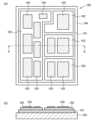
図1に、本発明の部分めっき用マスクを用いてめっき層の形成を終えた絶縁回路基板の平面図および断面図を模式的に例示する。図1(a)が平面図、図1(b)がA-A断面図である。セラミックスなどの絶縁板からなる絶縁基板101の片側表面上に、板状の金属部材102が接合されている。金属部材102は半導体素子を搭載するための回路用金属部材であり、この図の例では4枚の金属部材102が絶縁基板101上に島状に配置されている。それぞれの金属部材102の島は、絶縁基板101を介して他の部材から絶縁されている。すなわち、被めっき材である各金属部材102は電気的に孤立している。金属部材102の表面上には、本発明の部分めっき用マスクを使用して形成されためっき層103が存在する。本発明のマスクは、電気的に孤立している被めっき材(金属部材102)に、給電しながら電気めっきを施すために使用するものである。Figure 1 shows a schematic plan view and cross-sectional view of an insulating circuit board on which a plating layer has been formed using the partial plating mask of the present invention. Figure 1(a) is a plan view, and Figure 1(b) is an A-A cross-sectional view. A plate-shaped
めっき層103は、金属部材102の表面上の、半導体素子等の搭載位置に対応する部分に選択的に形成されている。このように、被めっき材の表面の所定部分のみに選択的に施すめっきを、本明細書では「部分めっき」と呼んでいる。金属部材102は通常、導電性の良好なアルミニウム系あるいは銅系の金属で構成される。上述のように、半導体素子を取り付けるための「はんだ付け性」を改善するために、めっきを施す必要が生じる。なお、図1(b)において、めっき層103の厚さは非常に誇張して描いてある。The
絶縁基板101の、金属部材102の背面側には、めっき層103を形成する前の段階において、放熱ベース104が接合されている。半導体装置として使用されるときには、半導体素子から発生する熱は絶縁基板101を介して放熱ベース104に伝わり、筐体や放熱器を通じて外部に放熱される。放熱ベース104は熱伝導性の良好なアルミニウム系あるいは銅系の金属材料を主体として構成されることが一般的である。この図の例では、放熱ベース104は周壁部105を有しており、周壁部105の表面高さと金属部材102の表面高さが概ね一致するように設計されている。すなわち、図1には、絶縁基板101と、回路用の金属部材102と、放熱ベース104が一体化した絶縁回路基板であって、特に金属部材102の表面と放熱ベース104の周壁部105の表面とが、概ね同一平面内にある絶縁回路基板100を例示してある。The
図2に、本発明の部分めっき用マスクの構造を模式的に例示する。図2(a)が平面図、図2(b)がA-A断面図である。ここでは、図1に示した絶縁回路基板100にめっき層103を形成する際に使用するマスクを例示した。図2(a)中には、めっき時に、図1の絶縁回路基板100における金属部材102および周壁部105と重なることになる領域を便宜的に破線で示してある。めっき時には、この部分めっき用マスク3の上面に、絶縁回路基板(図1の符号100)を、被めっき材である金属部材(図1の符号102)が下向きになるように重ねる。この図では1つの絶縁回路基板(図1の符号100)をカバーする大きさの部分めっき用マスク3を例示しているが、使用するめっき液槽の規模に応じて、複数の絶縁回路基板を同時にカバーする大きさの部分めっき用マスク3を適用してもよい。Figure 2 shows a schematic example of the structure of the partial plating mask of the present invention. Figure 2(a) is a plan view, and Figure 2(b) is an A-A cross-sectional view. Here, a mask used when forming a
部分めっき用マスク3は、絶縁シート部材1と、その厚さ方向片側の面の一部領域を被覆する導電シート部材2で構成される。絶縁シート部材1にはめっきを施す位置に対応した開口部10が形成されている。開口部10は絶縁シート部材1の厚さを貫通している。導電シート部材2は、電気的に孤立している金属部材(図1の符号102)の島と接触することにより、それらの島に給電するための部材である。図2の例では、2枚の導電シート部材2が絶縁シート部材1の表面に貼付されており、金属部材(図1の符号102)の島は、めっきを施さない表面部分でいずれかの導電シート部材2と接触するようになっている。外部の電源からの導電シート部材2への給電も、部分めっき用マスク3の表面に露出している導電シート部材2の表面を通じて行われる。この図の例では、2枚の導電シート部材2がそれぞれ絶縁回路基板の周壁部(図1の符号105)に接触することにより、放熱ベース(図1の符号104)を通じて給電するようになっている。被めっき材である金属部材の島のレイアウトに応じて、例えば島間のみの通電を担う導電シート部材2を設けることにより、他の島を経由して個々の島へ給電するようにしてもよい。The
絶縁シート部材1としては、切断加工が容易であり、適度な強度を有する材料を適用することが望ましい。また、絶縁回路基板との密着性を高めるため適度な弾性、柔軟性を有する材料であることがより好ましい。具体的には、絶縁性シリコーンゴムなどのシート材を適用することができる。絶縁シート部材1の厚さは例えば0.3~10mmとすることができ、1~5mm、更には2~4mmとすることがより好ましい。一方、導電シート部材2としては、金属板や、導電性シリコーンゴムなどを使用することができる。導電シート部材2を絶縁シート部材1の表面に貼付する方法としては、接着剤を使用する方法や、両面粘着テープなどの粘着部材を介して貼り付ける方法などが適用できる。金属板としては、アルミニウム、アルミニウム合金、銅、銅合金、チタン、チタン合金、ステンレス鋼などを使用することができる。導電シート部材2は、図2のように厚さ方向に見たときに長方形などの単純な形状によって、絶縁基板上の金属部材の島間をつなぐことが可能となる場合が実際にはほとんどであり、加工が容易である。As the insulating
図2(b)中に破線c1およびc2で表示した部分の拡大図を、それぞれ図2(c1)および(c2)に示す。寸法精度の高いめっき層を効率的に形成させる観点からは、絶縁シート部材1の表面と導電シート2の表面との間に生じる段差δをできるだけ小さくすることが有利となる。また、段差を生じている導電シート部材2の端部から、それに最も近い開口部10のまでの距離dをある程度確保することが有利となる。上記の段差δは、弾性変形分を考慮して1mm程度まで大きくても使用することができるが、0.7mm以下とすることがより好ましく、0.15mm以下とすることが更に好ましい。導電シート部材2を絶縁シート部材1の表面に貼付する図2のようなタイプの部分めっき用マスク3では、導電シート部材2として、できるだけ厚さの薄い材料を適用することが有効である。Enlarged views of the portions indicated by the dashed lines c1 and c2 in FIG. 2(b) are shown in FIG. 2(c1) and (c2), respectively. From the viewpoint of efficiently forming a plating layer with high dimensional accuracy, it is advantageous to make the step δ between the surface of the insulating
上記の段差が生じている場合(すなわち、δ>0である場合)、できるだけ寸法精度の高いめっき層103を形成させる観点に立てば、例えば下記(1)式および(2)式を満たすことが効果的であり、下記(1)式および(2)’式を満たすことがより効果的である。また、上記それぞれの場合において、下記(1)式に代えて下記(1)’式を適用することがより好ましい。
d>0 …(1)
d≧0.3 …(1)’
δ/d≦0.7 …(2)
δ/d≦0.15 …(2)’
ここで、dは導電シート部材2と開口部10の最短距離(mm)である。δは、導電シート部材2を有する側の絶縁シート部材1の露出表面の高さを基準高さh0=0(mm)とし、導電シート部材の高さをh1(mm)としたとき、δ=h1-h0で表される値である。 When the above-mentioned step occurs (i.e., when δ>0), from the viewpoint of forming a
d>0 ... (1)
d≧0.3 … (1) '
δ/d≦0.7…(2)
δ/d≦0.15…(2)'
Here, d is the shortest distance (mm) between the
上記のようにdとδの関係を規定することにより、絶縁シート部材1の素材として、例えばシリコーンゴムなどの弾性材料を使用すると、絶縁回路基板100を部分めっき用マスク3に押し付けている荷重によって、導電シート部材2の近傍で絶縁シート部材1が弾性変形するので、絶縁シート部材1と導電シート部材2をほぼ密着させることが可能となり、開口部10以外(絶縁シート部材1と導電シート部材2の隙間)へのめっき液の浸入を防できるため、より寸法精度の高いめっき層103を形成することができる。 By specifying the relationship between d and δ as described above, if an elastic material such as silicone rubber is used as the material for the insulating
図3に、図2に示した本発明の部分めっき用マスクと絶縁回路基板をめっき液槽に設置したときの断面構造を模式的に例示する。めっき液槽31の上部に部分めっき用マスク3が設置され、その上に絶縁回路基板100が設置されている。絶縁回路基板100には鉛直方向下向きに所定の荷重が付与されている。この図には、図2のA-A断面に対応する断面を示してある。部分めっき用マスク3の表面に露出している導電シート部材2が、絶縁回路基板100の金属部材102および周壁部105と接触している。めっき液槽31に電解液であるめっき液40を満たし、絶縁シート部材1に設けられた開口部10の部分で、被めっき材である金属部材102がめっき液40に浸る。絶縁回路基板100の構成部材である放熱ベース104は金属を主体とする導電材料であるため、カソード側の給電は、外部電源50から導線51、放熱ベース104、導電シート部材2を経由して、金属部材102へと行われる。一方、アノード側の給電は、外部電源50から、導線52を経由して、めっき液槽31内に設けられたアノード電極32へと行われる。なお、めっき液40を被めっき材である金属部材102に接触させる手法として、めっき液40を前記開口部10に向けてスプレーで噴射するなど他の公知の方法を適用してもよい。 3 shows a schematic cross-sectional structure of the partial plating mask of the present invention and the insulating circuit board shown in FIG. 2 when placed in a plating solution tank. The
この図の例では、導電シート部材2を絶縁シート部材1の表面に貼り付けることによって前述の段差δが生じている。そのため、絶縁シート部材1と被めっき材である金属部材102との間には、隙間21が生じる。めっき液40は隙間21の部分にも入り込むと考えられる。その場合、所定部分(開口部10に対応する部分)のみに選択的にめっきができないことや、めっき作業中に隙間21を通して外部にめっき液40が漏れ出すことなどが予想された。しかしながら、発明者らの詳細な研究によれば、隙間21の部分にめっき液40が入り込んでも、開口部10に対応する部分へのめっき金属の析出は、隙間21の部分への析出に比べ、圧倒的に多くなることがわかった。また、析出が進行して開口部10に対応する部分のめっき層の厚さが増すと、隙間21の部分への新たな液の供給(電解質の供給)が滞り、隙間21の部分での析出は生じにくくなってくることがわかった。さらに、隙間21を通して外部に漏れ出すめっき液40の量も、めっき作業の障害とならない程度に抑制することができ、実用的な電気めっき操業が可能であることも確認された。 In the example shown in this figure, the
絶縁シート部材1の素材として、例えばシリコーンゴムなどの弾性材料を使用すると、絶縁回路基板100を部分めっき用マスク3に押し付けている荷重によって、導電シート部材2の近傍で絶縁シート部材1が弾性変形するので、導電シート部材2に近い部分を除き、絶縁シート部材1と導電シート部材2をほぼ密着させることが可能となる。その場合、開口部10に対応する所定部分以外への析出をいっそう抑制した効率的な電気めっきが可能となる。すなわち、より寸法精度の高いめっき層103を効率的に形成させるうえで有利となる。 If an elastic material such as silicone rubber is used as the material for the insulating
なお、絶縁シート部材1の素材が柔らかすぎる場合や寸法が大きい場合はたわみが発生して絶縁回路基板100との所望の密着が不十分となる可能性もある。このような場合は図3において絶縁シート部材1の下側(めっき液側)に図示しない比較的硬い樹脂などのベース部材をさらに設けるのが好ましい。このベース部材は板状で、素材として絶縁シート部材1と比べて硬さの大きいシリコーンゴムやベークライト、アクリル、塩化ビニルなどを用いてもよい。また、絶縁シート部材の1の開口部に対応する部分はめっき液の接触が損なわれないように、ベース部材にも開口部が設けておく。このようなベース部材の上に絶縁シート部材1を積層したタイプの部分めっき用マスク3を使用することもできる。If the material of the insulating
図4に、導電シート部材が絶縁シート部材の表面に形成された凹部に嵌め込まれているタイプの本発明の部分めっき用マスクの断面構造を模式的に例示する。部分めっき用マスク3を厚さ方向から見た開口部10の配置および導電シート部材2の配置は図2(a)と同じである。図4に示した断面は、図2(a)のA-A断面に相当する。導電シート部材2は、絶縁シート部材1の片側の面に形成された凹部11の中に嵌め込まれている。この場合、絶縁シート部材1の表面と導電シート部材2の露出表面とをフラットにすることができる。図4の例では、両者の間の段差はなく、上述の段差δの値はゼロである。導電シート部材2の厚さが凹部11の深さよりも大きい場合にはδ>0となり、被めっき材である金属部材(図2の符号102)の表面との接触圧力を高めたい場合には有効である。δ>0の場合には、上述のように、上記(1)式および(2)式を満たすことが効果的であり、上記(1)式および(2)’式を満たすことがより効果的である。また、上記(1)式に代えて上記(1)’式を適用することがより好ましい。一方、導電シート部材2の厚さを凹部11の深さよりも小さくすることによって、意図的にδ<0とすることも可能である。そのような構造の部分めっき用マスクは、被めっき材である金属部材(図2の符号102)の表面に凸部があり、そこから給電を行う場合に有効である。Figure 4 shows a schematic cross-sectional structure of the partial plating mask of the present invention in which the conductive sheet member is fitted into a recess formed on the surface of the insulating sheet member. The arrangement of the
凹部11の中に導電シート部材2を固定する方法としては、導電シート部材2の端面と凹部11の壁面の間に生じる弾性的な応力のみを利用する方式(すなわち、嵌め込むのみ)としてもよいし、接着剤や粘着部材を用いる方式としてもよい。The method of fixing the
(凹部を有する絶縁シート部材の作製方法の例示)
凹部11を有する絶縁シート部材1は素材の絶縁シート板材を彫り込むことにより作製することができる。その他の比較的簡単な方法として、「貼り合わせ法」を挙げることができる。これは例えば以下のようなものである。絶縁シート部材1の凹部深さをt1(mm)、凹部の低面から裏面までの厚さをt2(mm)とする。絶縁シート部材1の厚さ(両側露出表面間の距離)はt1+t2である。厚さがt2であるフラットな表面を持つ第1の絶縁シートと、厚さがt1であり、凹部となる部分が打ち抜かれて開口部となっている第2の絶縁シートを用意し、それらを接着剤などによい貼り合わせることにより所定の凹部11を有する絶縁シート部材1が得られる。開口部10は、貼り合わせた後に形成してもよいし、予め第1の絶縁シートと第2の絶縁シートの所定位置に開口部10に対応する開口を形成しておいてもよい。凹部のレイアウトによっては、第2の絶縁シートを独立した複数のシート部材で構成し、それらを第1の絶縁シートの所定位置に貼り付けることによって凹部11を形成してもよい。(Example of a method for producing an insulating sheet member having a recess)
The insulating
図5に、図4に示した本発明の部分めっき用マスクと絶縁回路基板をめっき液槽に設置したときの断面構造を模式的に例示する。この図には、図4の断面図に対応する断面を示してある。全体の構成は図3の場合と同様であるが、図5の例では導電シート部材2の表面と絶縁シート部材1の表面との間に段差がない(δ=0である)ことから、マスクの絶縁シート部材1と被めっき材である金属部材102との間には隙間(図3の符号21に相当する部分)が生じない。すなわち、金属部材102の表面は、開口部10の部分を除く全ての領域で絶縁シート部材1および導電シート部材2と密着している。開口部10に面する所定領域のみにめっき金属が析出するので、他の部分への析出に伴う電流損失がなく、より寸法精度の高いめっき層を形成することができる。 FIG. 5 shows a schematic cross-sectional structure of the partial plating mask and insulating circuit board of the present invention shown in FIG. 4 when placed in a plating solution tank. This figure shows a cross section corresponding to the cross section of FIG. 4. The overall structure is the same as that of FIG.3 , but in the example of FIG. 5, there is no step between the surface of the
図6に、本発明の部分めっき用マスクを用いてめっき層の形成を終えた絶縁回路基板(周壁部がないタイプ)の平面図および断面図を模式的に例示する。図6(a)が平面図、図6(b)がA-A断面図である。この絶縁回路基板100は、金属部材102とめっき層103の配置、および各部材の積層構造は図1のものと同様であるが、放熱ベース104に周壁部(図1の符号105に相当する部分)がないタイプである。なお、図6(b)において、めっき層103の厚さは非常に誇張して描いてある。Figure 6 shows a schematic plan view and cross-sectional view of an insulated circuit board (without peripheral walls) after the formation of a plating layer using the partial plating mask of the present invention. Figure 6(a) is a plan view, and Figure 6(b) is an A-A cross-sectional view. This
図7に、図6に示した絶縁回路基板にめっき層を形成する際に使用するための本発明の部分めっき用マスクの構造を模式的に例示する。図7(a)が平面図、図7(b)がA-A断面図である。図7(a)中には、めっき時に、図6の絶縁回路基板100における金属部材102と重なることになる領域を便宜的に破線で示してある。この部分めっき用マスク3は、導電シート部材2が絶縁シート部材1の表面に形成された凹部11に嵌め込まれているタイプである。断面構造においては、図4の例と同様に、導電シート部材2の表面と絶縁シート部材1の表面との間に段差がない(δ=0である)。Figure 7 shows a schematic example of the structure of the partial plating mask of the present invention for use in forming a plating layer on the insulating circuit board shown in Figure 6. Figure 7(a) is a plan view, and Figure 7(b) is an A-A cross-sectional view. In Figure 7(a), the area that will overlap with the
図8に、図7に示した本発明の部分めっき用マスクと絶縁回路基板をめっき液槽に設置したときの断面構造を模式的に例示する。この図には、図7のA-A断面に対応する断面を示してある。図5の例と同様、金属部材102の表面は、開口部10の部分を除く全ての領域で絶縁シート部材1および導電シート部材2と密着している。ただし、放熱ベース104には周壁部(図5の符号105)がない。そのため、放熱ベース104を経由して直接的に導電シート部材2へと給電することはできない。このような場合には、図示のように、導電シート部材2の露出面の一部にカソード側の外部電極60を接触させることにより給電を行うことができる。カソード側の給電は、外部電源50から導線51、外部電極60、導電シート部材2を経由して、金属部材102へと行われる。一方、アノード側の給電は図3の場合と同様に、外部電源50から、導線52を経由して、めっき液槽31内に設けられたアノード電極32へと行われる。 FIG. 8 shows a schematic cross-sectional structure of the partial plating mask and insulating circuit board of the present invention shown in FIG. 7 when placed in a plating solution tank. This figure shows a cross section corresponding to the A-A cross section in FIG. 7. As in the example of FIG. 5, the surface of the
なお、前記絶縁回路基板またはその中間製品としては、絶縁基板がセラミックス板であり、その絶縁基板のめっき層を形成させる回路用金属部材の背面側に、放熱部材を備えるものを適用することもできる。そのセラミックス板は窒化アルミニウム(AlN)、窒化ケイ素、アルミナなどを主成分とするものが好ましく、回路用金属部材および放熱部材はアルミニウムまたはアルミニウム合金、銅または銅合金であることが好ましい。セラミックス基板と、回路用金属部材および放熱部材との接合方法は公知の手法を用いればよい。例えば、ろう材を用いて接合するろう接法、所定の雰囲気中で部材同士接触加熱することで接合する直接接合法、セラミックス基板を鋳型内に配置して金属溶湯を流し込んだのち凝固させて接合する溶湯接合法などが挙げられる。 The insulating circuit board or intermediate product thereof may be an insulating board made of a ceramic plate, and a heat dissipation member may be provided on the back side of the metal circuit member on which the plating layer of the insulating board is formed. The ceramic plate is preferably made of aluminum nitride (AlN), silicon nitride, alumina, or the like, and the metal circuit member and the heat dissipation member are preferably made of aluminum or an aluminum alloy, copper or a copper alloy. The method of joining the ceramic board to the metal circuitmember and the heat dissipation member may be a known method. For example, a brazing method using a brazing material for joining, a direct joining method in which the members are joined by contacting and heating each other in a specified atmosphere, and a molten metal joining method in which the ceramic board is placed in a mold, molten metal is poured in, and then solidified to join the ceramic board.
[実施例1]
図1に示したものと同様の積層構造を有する絶縁回路基板(ただし、めっき層がまだ形成されていないもの)を用意した。金属部材(図1の符号102)の配置も図1のものと類似している。金属部材の各島は絶縁基板上でそれぞれ電気的に孤立している。絶縁基板(図1の符号101)は寸法67mm×71mm×0.6mmの窒化アルミニウム板である。その上に接合されている金属部材(図1の符号102)は純度99.9%の純アルミニウムからなる厚さ1.3mmの板材である。絶縁基板の裏面に接合されている放熱ベース(図1の符号104)も純度99.9%の純アルミニウムからなり、上記金属部材の表面とほぼ同じ高さの周壁部(図1の符号105)を有する。放熱ベースの厚さは絶縁基板の裏面部分において3mmである。なお、窒化アルミニウム板と、アルミニウムからなる金属部材および放熱ベースとは、溶湯接合法により接合されている。[Example 1]
An insulating circuit board having a laminated structure similar to that shown in FIG. 1 (but on which a plating layer has not yet been formed) was prepared. The arrangement of the metal members (
上記の絶縁回路基板を2個並べて電気部分めっきに供するためのマスクとして、図4に示したような、導電シート部材(図4の符号2)が絶縁シート部材(図4の符号1)の表面に形成された凹部(図4の符号11)に嵌め込まれているタイプの部分めっき用マスクを以下のようにして作製した。As a mask for electrically plating two of the above insulating circuit boards side by side, a partial plating mask of the type shown in FIG. 4 in which a conductive sheet member (
絶縁シート部材は、上掲の「凹部を有する絶縁シート部材の作製方法の例示」に記載したように、フラットな形状を有する第1の絶縁シートと、凹部に相当する部分に開口を形成した第2の絶縁シートを貼り合わせる「貼り合わせ法」によって作製した。絶縁シートの材質は絶縁性シリコーンゴムである。貼り合わせた後に、めっきを施す部分に対応する開口部(図4の符号10)を形成した。得られた絶縁シート部材の厚さ(凹部以外の部分)は4mmであり、凹部の深さは1mm、幅は7mm、長さは64mmである。絶縁回路基板を2個並べてマスキングできるように、厚さ方向に見た絶縁シート部材の寸法は280mm×100mmとした。The insulating sheet member was produced by the "lamination method" in which a first insulating sheet having a flat shape and a second insulating sheet having an opening formed in the part corresponding to the recess are laminated together, as described above in "Example of a method for producing an insulating sheet member having a recess". The insulating sheet material is insulating silicone rubber. After lamination, an opening (10 in Figure 4) corresponding to the part to be plated is formed. The thickness of the obtained insulating sheet member (parts other than the recess) is 4 mm, and the recess has a depth of 1 mm, a width of 7 mm, and a length of 64 mm. The dimensions of the insulating sheet member in the thickness direction are 280 mm x 100 mm so that two insulating circuit boards can be arranged side by side and masked.
導電シート部材として、寸法64mm×7mm×1mmのチタン板を4枚用意した。このチタン板の体積抵抗率は42μΩ・cmである。これらを上記絶縁シート部材の凹部に嵌め込んで、給電機能を有する部分めっき用マスクとした。導電シート部材の固定は凹部に嵌め込むことにより生じる絶縁性シリコーンゴムの弾性力のみで賄った。導電シート部材と絶縁シート部材の間に段差はない(δ=0)。また、導電シート部材の端部から、それに最も近い開口部までの距離dは、いずれの導電シート部材についても約1mmである。Four titanium plates measuring 64 mm x 7 mm x 1 mm were prepared as conductive sheet members. The volume resistivity of these titanium plates was 42 μΩ·cm. These were fitted into the recesses of the insulating sheet member described above to form a partial plating mask with a power supply function. The conductive sheet members were fixed only by the elastic force of the insulating silicone rubber generated by fitting them into the recesses. There was no step between the conductive sheet member and the insulating sheet member (δ = 0). Furthermore, the distance d from the edge of the conductive sheet member to the opening closest to it was approximately 1 mm for each conductive sheet member.
この部分めっき用マスクをめっき液槽に設置し、その上に上記の絶縁回路基板を2個設置した。そのときの断面構造は概ね図5と同様である。図5に表示した断面の背後に、もう一つの絶縁回路基板がセットされている状態となっている。2個の絶縁回路基板にそれぞれ所定の荷重を付与することにより、絶縁回路基板と部分めっき用マスクの密着性を維持した。アノード電極(図5の符号32)としてチタンを使用した。めっき液はNiめっき液(ワット浴)、めっき温度は50℃とした。This partial plating mask was placed in a plating solution tank, and two of the above-mentioned insulating circuit boards were placed on top of it. The cross-sectional structure at this point was roughly the same as that shown in Figure 5. Another insulating circuit board was set behind the cross section shown in Figure 5. A specified load was applied to each of the two insulating circuit boards to maintain adhesion between the insulating circuit board and the partial plating mask. Titanium was used as the anode electrode (
このようにして、平均厚さ10μmのめっき層を形成させた(以下の各例において同じ)。めっき後の絶縁回路基板を観察したところ、マスク開口部からのめっき液の滲出は全く見られず、寸法精度の高いめっきが実現できた。In this way, a plating layer with an average thickness of 10 μm was formed (the same applies to each of the following examples). When the insulating circuit board was observed after plating, no leakage of plating solution from the mask openings was observed, and plating with high dimensional accuracy was achieved.
[実施例2]
導電シート部材として導電性シリコーンゴムシートを使用したことを除き、実施例1と同様の条件で絶縁回路基板の所定部分に電気Niめっきを施した。この導電性シリコーンゴムシートの体積抵抗率は10Ω・cmである。めっき後の絶縁回路基板を観察したところ、滲出は全く見られず、寸法精度の高いめっきが実現できた。
なお、導電シート部材として導電性シリコーンゴムシートを使用すると液漏れ防止効果が高いので、導電シート部材がめっき液と反応しにくい。導電性シリコーンゴムシートは安価であるため、高価なチタン板を使用しなくても長寿命化が可能であるという利点を有する。[Example 2]
Except for using a conductive silicone rubber sheet as the conductive sheet member, electric Ni plating was applied to a predetermined portion of an insulating circuit board under the same conditions as in Example 1. The volume resistivity of this conductive silicone rubber sheet was 10 Ω cm. When the insulating circuit board after plating was observed, no exudation was observed, and plating with high dimensional accuracy was achieved.
In addition, when a conductive silicone rubber sheet is used as the conductive sheet member, the leakage prevention effect is high, so the conductive sheet member is less likely to react with the plating solution. Since the conductive silicone rubber sheet is inexpensive, it has the advantage of being able to extend the life without using expensive titanium plates.
[実施例3]
部分めっき用マスクとして、絶縁シート部材の凹部に導電シート部材を嵌め込むタイプに代えて、図2に示したような、凹部のないフラットな絶縁シート部材の表面に導電シート部材を貼付するタイプを採用した。また、導電シート部材の材質をSUS304とし、その厚さを0.01mmとした。それ以外は実施例1と同様の方法で絶縁回路基板の所定部分に電気Niめっきを施した。[Example 3]
As a partial plating mask, instead of a type in which a conductive sheet member is fitted into a recess in an insulating sheet member, a type in which a conductive sheet member is attached to the surface of a flat insulating sheet member without a recess, as shown in Fig. 2, was adopted. In addition, the material of the conductive sheet member was SUS304, and its thickness was 0.01 mm. Otherwise, electric Ni plating was applied to the specified parts of the insulating circuit board in the same manner as in Example 1.
部分めっき用マスクの絶縁シート部材の厚さは4mmである。導電シート部材として使用したSUS304板の体積抵抗率は72μΩ・cmである。部分めっき用マスクを厚さ方向に見た導電シート部材の配置および開口部の配置は、実施例1と同じである。したがって、導電シート部材の端部から、それに最も近い開口部までの距離dは、いずれの導電シート部材についても約1mmである。SUS304板を絶縁シート部材(絶縁性シリコーンゴムシート)の表面に貼り付ける方法は、両面粘着テープ(ニチバン社製、ナイスタック、厚さ0.09mm)を介する貼付方法とした。導電シート部材の表面と絶縁シート部材の露出表面の段差δは約0.1mmである。部分めっき用マスクをめっき液槽に設置し、その上に2個の絶縁回路基板を設置したときの断面構造は概ね図3と同様である。図3に表示した断面の背後に、もう一つの絶縁回路基板がセットされている状態となっている。The thickness of the insulating sheet member of the partial plating mask is 4 mm. The volume resistivity of the SUS304 plate used as the conductive sheet member is 72 μΩ·cm. The arrangement of the conductive sheet member and the arrangement of the openings when the partial plating mask is viewed in the thickness direction are the same as in Example 1. Therefore, the distance d from the end of the conductive sheet member to the nearest opening is about 1 mm for each conductive sheet member. The SUS304 plate was attached to the surface of the insulating sheet member (insulating silicone rubber sheet) using a double-sided adhesive tape (Nichiban Co., Ltd., Nicetack, thickness 0.09 mm). The step δ between the surface of the conductive sheet member and the exposed surface of the insulating sheet member is about 0.1 mm. The cross-sectional structure when the partial plating mask is placed in the plating solution tank and two insulating circuit boards are placed on it is generally the same as that shown in Figure 3. Another insulating circuit board is set behind the cross section shown in Figure 3.
めっき後の絶縁回路基板を観察したところ、マスク開口部からめっき液の滲出が認められ、めっき箇所の縁にはめっき金属(Ni)のにじみがごく僅かに見られた。しかし、めっき液の滲出はめっき作業上問題のない程度であり、得られためっき層の寸法精度についても実用上問題はないと判断された。When the insulated circuit board after plating was observed, seepage of plating solution was observed from the mask openings, and very slight bleeding of the plating metal (Ni) was observed on the edges of the plated areas. However, the seepage of plating solution was not significant enough to cause any problems in the plating process, and it was determined that the dimensional accuracy of the resulting plating layer did not pose any practical problems.
[実施例4]
フラットな絶縁シート部材の表面に貼付する導電シート部材として、厚さ0.03mmのSUS304板を使用したことを除き、実施例3と同様の条件で絶縁回路基板の所定部分に電気Niめっきを施した。このSUS304板の体積抵抗率は72μΩ・cmである。上述の段差δは約0.12mmである。めっき後の絶縁回路基板を観察したところ、マスク開口部からめっき液の滲出が認められ、めっき箇所の縁にはめっき金属(Ni)のにじみがごく僅かに見られた。しかし、めっき液の滲出はめっき作業上問題のない程度であり、得られためっき層の寸法精度についても実用上問題はないと判断された。[Example 4]
A predetermined portion of an insulated circuit board was electroplated with Ni under the same conditions as in Example 3, except that a SUS304 plate with a thickness of 0.03 mm was used as the conductive sheet member to be attached to the surface of the flat insulating sheet member. The volume resistivity of this SUS304 plate was 72 μΩ·cm. The above-mentioned step δ was about 0.12 mm. When the insulated circuit board after plating was observed, seepage of the plating solution was observed from the mask opening, and very slight bleeding of the plating metal (Ni) was observed on the edges of the plated areas. However, the seepage of the plating solution was not significant enough to cause any problems in the plating work, and it was determined that the dimensional accuracy of the obtained plating layer did not cause any practical problems.
[実施例5]
フラットな絶縁シート部材の表面に貼付する導電シート部材として、厚さ0.05mmのSUS304板を使用したことを除き、実施例3と同様の条件で絶縁回路基板の所定部分に電気Niめっきを施した。このSUS304板の体積抵抗率は72μΩ・cmである。上述の段差δは約0.14mmである。めっき後の絶縁回路基板を観察したところ、マスク開口部からめっき液の滲出が認められ、めっき箇所の縁にはめっき金属(Ni)のにじみがところどころに見られた。しかし、めっき液の滲出はめっき作業上問題のない程度であり、得られためっき層の寸法精度についても実用上問題はないと判断された。[Example 5]
Electrical Ni plating was applied to a predetermined portion of an insulated circuit board under the same conditions as in Example 3, except that a SUS304 plate with a thickness of 0.05 mm was used as the conductive sheet member to be attached to the surface of the flat insulating sheet member. The volume resistivity of this SUS304 plate was 72 μΩ·cm. The above-mentioned step δ was about 0.14 mm. When the insulated circuit board after plating was observed, seepage of plating solution was observed from the mask opening, and bleeding of plating metal (Ni) was observed in places on the edges of the plated areas. However, the seepage of plating solution was not to the extent that it would cause any problems in the plating work, and it was determined that the dimensional accuracy of the obtained plating layer would not cause any practical problems.
[実施例6]
フラットな絶縁シート部材の表面に貼付する導電シート部材として、厚さ0.1mmのSUS304板を使用したことを除き、実施例3と同様の条件で絶縁回路基板の所定部分に電気Niめっきを施した。このSUS304板の体積抵抗率は72μΩ・cmである。上述の段差δは約0.19mmである。めっき後の絶縁回路基板を観察したところ、マスク開口部からめっき液の滲出が認められ、めっき箇所の縁にはめっき金属(Ni)のにじみが全体的に見られた。しかし、めっき液の滲出はめっき作業上問題のない程度であり、得られためっき層の寸法精度についても実用上問題はないと判断された。[Example 6]
A predetermined portion of an insulated circuit board was electroplated with Ni under the same conditions as in Example 3, except that a SUS304 plate with a thickness of 0.1 mm was used as the conductive sheet member to be attached to the surface of the flat insulating sheet member. The volume resistivity of this SUS304 plate was 72 μΩ·cm. The above-mentioned step δ was about 0.19 mm. When the insulated circuit board after plating was observed, seepage of the plating solution was observed from the mask opening, and bleeding of the plating metal (Ni) was observed all over the edges of the plated areas. However, the seepage of the plating solution was not significant enough to cause any problems in the plating work, and it was determined that the dimensional accuracy of the obtained plating layer did not cause any practical problems.
[実施例7]
フラットな絶縁シート部材の表面に貼付する導電シート部材として、厚さ0.1mmの鉛板を使用したことを除き、実施例3と同様の条件で絶縁回路基板の所定部分に電気Niめっきを施した。この鉛板の体積抵抗率は20.8μΩ・cmである。上述の段差δは約0.19mmである。めっき後の絶縁回路基板を観察したところ、マスク開口部からめっき液の滲出が認められ、めっき箇所の縁にはめっき金属(Ni)のにじみが全体的に見られた。しかし、めっき液の滲出はめっき作業上問題のない程度であり、得られためっき層の寸法精度についても実用上問題はないと判断された。[Example 7]
Electrical Ni plating was applied to a predetermined portion of an insulated circuit board under the same conditions as in Example 3, except that a lead plate with a thickness of 0.1 mm was used as the conductive sheet member to be attached to the surface of the flat insulating sheet member. The volume resistivity of this lead plate was 20.8 μΩ·cm. The above-mentioned step δ was about 0.19 mm. When the insulated circuit board after plating was observed, seepage of plating solution was observed from the mask opening, and bleeding of plating metal (Ni) was observed all over the edges of the plated areas. However, the seepage of plating solution was not to the extent that it would cause any problems in the plating work, and it was determined that the dimensional accuracy of the obtained plating layer would not cause any practical problems.
[実施例8]
フラットな絶縁シート部材の表面に貼付する導電シート部材として、厚さ0.5mmの導電性シリコーンゴムシートを使用したことを除き、実施例3と同様の条件で絶縁回路基板の所定部分に電気Niめっきを施した。この導電性シリコーンゴムシートの体積抵抗率は10Ω・cmである。上述の段差δは約0.59mmである。めっき後の絶縁回路基板を観察したところ、マスク開口部からめっき液の滲出が認められ、めっき箇所の縁にはめっき金属(Ni)のにじみが全体的に見られた。しかし、めっき液の滲出はめっき作業上問題のない程度であり、得られためっき層の寸法精度についても実用上問題はないと判断された。[Example 8]
Electric Ni plating was applied to a predetermined portion of an insulating circuit board under the same conditions as in Example 3, except that a conductive silicone rubber sheet with a thickness of 0.5 mm was used as the conductive sheet member to be attached to the surface of the flat insulating sheet member. The volume resistivity of this conductive silicone rubber sheet was 10 Ω·cm. The above-mentioned step δ was about 0.59 mm. When the insulating circuit board after plating was observed, seepage of plating solution was observed from the mask opening, and bleeding of plating metal (Ni) was observed all over the edges of the plated areas. However, the seepage of plating solution was not to the extent that it would cause any problems in the plating work, and it was determined that the dimensional accuracy of the obtained plating layer would not cause any practical problems.
[実施例9]
フラットな絶縁シート部材の表面に貼付する導電シート部材として、厚さ0.05mmのアルミニウム板を使用したことを除き、実施例3と同様の条件で絶縁回路基板の所定部分に電気Niめっきを施した。このアルミニウム板の体積抵抗率は2.7μΩ・cmである。上述の段差δは約0.14mmである。めっき後の絶縁回路基板を観察したところ、マスク開口部からめっき液の滲出が認められ、めっき箇所の縁にはめっき金属(Ni)のにじみがところどころに見られた。しかし、めっき液の滲出はめっき作業上問題のない程度であり、得られためっき層の寸法精度についても実用上問題はないと判断された。[Example 9]
A predetermined portion of an insulating circuit board was electroplated with Ni under the same conditions as in Example 3, except that an aluminum plate with a thickness of 0.05 mm was used as the conductive sheet member to be attached to the surface of the flat insulating sheet member. The volume resistivity of this aluminum plate was 2.7 μΩ·cm. The above-mentioned step δ was about 0.14 mm. When the insulating circuit board after plating was observed, seepage of plating solution was observed from the mask opening, and bleeding of plating metal (Ni) was observed in places on the edges of the plated areas. However, the seepage of plating solution was not to the extent that it would cause any problems in the plating work, and it was determined that the dimensional accuracy of the obtained plating layer would not cause any practical problems.
[実施例10]
フラットな絶縁シート部材の表面に貼付する導電シート部材として、厚さ0.05mmの銅板を使用したことを除き、実施例3と同様の条件で絶縁回路基板の所定部分に電気Niめっきを施した。この銅板の体積抵抗率は1.7μΩ・cmである。上述の段差δは約0.14mmである。めっき後の絶縁回路基板を観察したところ、マスク開口部からめっき液の滲出が認められ、めっき箇所の縁にはめっき金属(Ni)のにじみがところどころに見られた。しかし、めっき液の滲出はめっき作業上問題のない程度であり、得られためっき層の寸法精度についても実用上問題はないと判断された。[Example 10]
Electric Ni plating was applied to a predetermined portion of an insulating circuit board under the same conditions as in Example 3, except that a copper plate with a thickness of 0.05 mm was used as the conductive sheet member to be attached to the surface of the flat insulating sheet member. The volume resistivity of this copper plate was 1.7 μΩ·cm. The above-mentioned step δ was about 0.14 mm. When the insulating circuit board after plating was observed, seepage of plating solution was observed from the mask opening, and bleeding of plating metal (Ni) was observed in places on the edges of the plated areas. However, the seepage of plating solution was not to the extent that it would cause any problems in the plating work, and it was determined that the dimensional accuracy of the obtained plating layer would not cause any practical problems.
[実施例11]
フラットな絶縁シート部材の表面に貼付する導電シート部材として、厚さ0.05mmのアルミニウム板を使用し、開口部10のまでの距離dをゼロにしたことを除き、実施例3と同様の条件で絶縁回路基板の所定部分に電気Niめっきを施した。この銅板の体積抵抗率は2.7μΩ・cmである。上述の段差δは約0.14mmである。この場合、導電シート部材の端面に付着しためっき金属の量が他の実施例より多かった。寸法精度の確保、異物の混入抑制を考慮すると、マスク寿命は他の実施例より短くなると考えられる。めっき後の絶縁回路基板を観察したところ、マスク開口部からめっき液の滲出が認められ、めっき箇所の縁にはめっき金属(Ni)のにじみがところどころ見られた。しかし、めっき液の滲出はめっき作業上問題のない程度であり、得られためっき層の寸法精度についても実用上問題はないと判断された。[Example 11]
An aluminum plate having a thickness of 0.05 mm was used as the conductive sheet member to be attached to the surface of the flat insulating sheet member, and electric Ni plating was applied to a predetermined portion of the insulating circuit board under the same conditions as in Example 3, except that the distance d to the
以上の各実施例においては、めっき対象である絶縁回路基板は、めっき前の段階で各金属部材の島が電気的に孤立しているので、めっき工程あるいはその後の工程で手間の掛かるレジスト膜の形成および除去を行う必要がない。また、孤立した島への給電機能を有する本発明の部分めっき用マスクは、簡単な構造を採用しているにもかかわらず、工業的な量産に十分対応できる性能を発揮することが確認された。In each of the above examples, the islands of each metal member of the insulating circuit board to be plated are electrically isolated at the stage prior to plating, so there is no need to perform the time-consuming formation and removal of a resist film during the plating process or subsequent processes. In addition, it has been confirmed that the partial plating mask of the present invention, which has a function of supplying power to the isolated islands, exhibits performance sufficient for industrial mass production, despite employing a simple structure.
1 絶縁シート部材
2 導電シート部材
3 部分めっき用マスク
10 開口部
11 凹部
21 隙間
31 めっき液槽
32 アノード電極
40 めっき液
50 外部電源
51、52 導線
60 外部電極
100 絶縁回路基板
101 絶縁基板
102 金属部材
103 めっき層
104 放熱ベース
105 周壁部 REFERENCE SIGNS
Claims (13)
Translated fromJapanese前記所定部分に対応する形状の開口部が形成された絶縁シート部材の、厚さ方向片側の面の一部領域が、その領域に取り付けられた1つまたは複数の導電シート部材で被覆された構造を有し、前記導電シート部材は、そのシートの片面全体が前記絶縁シート部材の外部に露出している、部分めっき用マスク。 A partial plating mask for selectively electroplating a predetermined portion of a surface of one or more electrically isolated metal members formed on an insulating substrate, the mask being used to bring the predetermined portion into contact with a plating solution, the mask comprising:
A partial plating mask having a structure in which a portion of one surface in the thickness direction of an insulating sheet member having an opening of a shape corresponding to the specified portion is covered with one or more conductive sheet members attached to that area,and the conductive sheet member has one entire side of the sheet exposed to the outside of the insulating sheet member .
請求項1~3のいずれか1項に記載の部分めっき用マスクを使用し、
当該マスクに形成されている開口部を、めっき層を形成させる前記回路用金属部材の表面のめっきを施す所定部分に配置して、前記所定部分をめっき液と接触させるとともに、
当該マスク表面に露出している導電シート部材を、めっき層を形成させる前記回路用金属部材の表面のめっきを施さない部分と、外部電源に導通する電極とに接触させた状態とし、
前記導電シート部材を通じて、めっき層を形成させる前記回路用金属部材に給電を行いながら電気めっきを行う、絶縁回路基板の製造方法。 A method for producing an insulating circuit board having a metal circuit member on which a plating layer is formed by selectively electroplating a predetermined portion of a surface of the metal circuit member of an intermediate insulating circuit board product including an insulating substrate and one or more electrically isolated metal circuit members formed on one surface of the insulating substrate, comprising:
Using the partial plating mask according to any one of claims 1 to 3,
An opening formed in the mask is placed at a predetermined portion of the surface of the metal component for circuits on which a plating layer is to be formed, and the predetermined portion is brought into contact with a plating solution;
the conductive sheet member exposed on the mask surface is brought into contact with a portion of the surface of the metal member for circuits on which a plating layer is to be formed that is not to be plated and with an electrode that is conductive to an external power source;
A method for producing an insulated circuit board, comprising the steps of: performing electroplating while supplying power to the circuit metal member on which a plating layer is to be formed, through the conductive sheet member.
下記(A)に記載の部分めっき用マスクを使用し、
当該マスクに形成されている開口部を、めっき層を形成させる前記回路用金属部材の表面のめっきを施す所定部分に配置して、前記所定部分をめっき液と接触させるとともに、
当該マスク表面に露出している導電シート部材を、めっき層を形成させる前記回路用金属部材の表面のめっきを施さない部分と、外部電源に導通する電極とに接触させた状態とし、
前記導電シート部材を通じて、めっき層を形成させる前記回路用金属部材に給電を行いながら電気めっきを行う、絶縁回路基板の製造方法であって、
前記絶縁回路基板の中間製品は、絶縁基板がセラミックス板であり、その絶縁基板のめっき層を形成させる回路用金属部材の背面側に、放熱部材を備えるものであり、
前記放熱部材は前記絶縁基板の端面の一部または全部を囲む周壁部を有する導体であり、外部電源に導通する前記電極として当該放熱部材の周壁部を利用し、前記導電シート部材をその周壁部に接触させることにより、めっき層を形成させる前記回路用金属部材に給電を行う、絶縁回路基板の製造方法。
(A)絶縁基板上に形成された1つまたは複数の電気的に孤立している金属部材の表面の所定部分に選択的に電気めっきを施す際に使用する、前記所定部分をめっき液と接触させるための部分めっき用マスクであって、
前記所定部分に対応する形状の開口部が形成された絶縁シート部材の、厚さ方向片側の面の一部領域が、その領域に取り付けられた1つまたは複数の導電シート部材で被覆された構造を有する部分めっき用マスク。A method for producing an insulating circuit board having a metal circuit member on which a plating layer is formed by selectively electroplating a predetermined portion of a surface of the metal circuit member of an intermediate insulating circuit board product including an insulating substrate and one or more electrically isolated metal circuit members formed on one surface of the insulating substrate, comprising:
Using the partial plating mask described in (A) below,
An opening formed in the mask is placed at a predetermined portion of the surface of the metal component for circuits on which a plating layer is to be formed, and the predetermined portion is brought into contact with a plating solution;
the conductive sheet member exposed on the mask surface is brought into contact with a portion of the surface of the metal member for circuits on which a plating layer is to be formed that is not to be plated and with an electrode that is conductive to an external power source;
A method for producing an insulated circuit board, comprising the steps of: supplying electricity to the circuit metal member on which a plating layer is to be formed through the conductive sheet member while electroplating is performed,
The intermediate insulating circuit board product has an insulating substrate which is a ceramic plate, and a heat dissipation member provided on the back side of a metal member for circuits on which a plating layer of the insulating substrate is formed,
The heat dissipation member is a conductor having a peripheral wall portion that surrounds part or all of an end face of the insulatingsubstrate , and the peripheral wall portion of the heat dissipation member is used as the electrode that is conductive to an external power source, and the conductive sheet member is brought into contact with the peripheral wall portion to supply power to the circuit metal member that forms a plating layer.
(A) A partial plating mask used when selectively electroplating predetermined portions of a surface of one or more electrically isolated metal members formed on an insulating substrate, for bringing the predetermined portions into contact with a plating solution, comprising:
A partial plating mask having a structure in which a portion of a surface on one side in the thickness direction of an insulating sheet member having an opening of a shape corresponding to the specified portion is covered with one or more conductive sheet members attached to that area.
請求項1~3のいずれか1項に記載の部分めっき用マスクを使用し、
当該マスクに形成されている開口部を、めっき層を形成させる前記回路用金属部材の表面のめっきを施す所定部分に配置して、前記所定部分をめっき液と接触させるとともに、
当該マスク表面に露出している導電シート部材を、めっき層を形成させる前記回路用金属部材の表面のめっきを施さない部分と、外部電源に導通する電極とに接触させた状態とし、
前記導電シート部材を通じて、めっき層を形成させる前記回路用金属部材に給電を行いながら電気めっきを行う、部分めっき方法。 A partial plating method for selectively electroplating a predetermined portion of a surface of one or more electrically isolated metal members for a circuit formed on one surface of an insulating substrate, comprising the steps of:
Using the partial plating mask according to any one of claims 1 to 3,
An opening formed in the mask is placed at a predetermined portion of the surface of the metal component for circuits on which a plating layer is to be formed, and the predetermined portion is brought into contact with a plating solution;
the conductive sheet member exposed on the mask surface is brought into contact with a portion of the surface of the metal member for circuits on which a plating layer is to be formed that is not to be plated and with an electrode that is conductive to an external power source;
A selective plating method in which electroplating is performed while supplying electricity to the metal circuit member on which a plating layer is to be formed through the conductive sheet member.
下記(A)に記載の部分めっき用マスクを使用し、
当該マスクに形成されている開口部を、めっき層を形成させる前記回路用金属部材の表面のめっきを施す所定部分に配置して、前記所定部分をめっき液と接触させるとともに、
当該マスク表面に露出している導電シート部材を、めっき層を形成させる前記回路用金属部材の表面のめっきを施さない部分と、外部電源に導通する電極とに接触させた状態とし、
前記導電シート部材を通じて、めっき層を形成させる前記回路用金属部材に給電を行いながら電気めっきを行う、部分めっき方法であって、
前記絶縁基板は、セラミックス板であり、めっき層を形成させる回路用金属部材の背面側に、放熱部材を備えるものであり、
前記放熱部材は前記絶縁基板の端面の一部または全部を囲む周壁部を有する導体であり、外部電源に導通する前記電極として当該放熱部材の周壁部を利用し、前記導電シート部材をその周壁部に接触させることにより、めっき層を形成させる前記回路用金属部材に給電を行う、部分めっき方法。
(A)絶縁基板上に形成された1つまたは複数の電気的に孤立している金属部材の表面の所定部分に選択的に電気めっきを施す際に使用する、前記所定部分をめっき液と接触させるための部分めっき用マスクであって、
前記所定部分に対応する形状の開口部が形成された絶縁シート部材の、厚さ方向片側の面の一部領域が、その領域に取り付けられた1つまたは複数の導電シート部材で被覆された構造を有する部分めっき用マスク。A partial plating method for selectively electroplating a predetermined portion of a surface of one or more electrically isolated metal members for a circuit formed on one surface of an insulating substrate, comprising the steps of:
Using the partial plating mask described in (A) below,
An opening formed in the mask is placed at a predetermined portion of the surface of the metal component for circuits on which a plating layer is to be formed, and the predetermined portion is brought into contact with a plating solution;
the conductive sheet member exposed on the mask surface is brought into contact with a portion of the surface of the metal member for circuits on which a plating layer is to be formed that is not to be plated and with an electrode that is conductive to an external power source;
A selective plating method for performing electroplating while supplying electricity to the circuit metal member on which a plating layer is to be formed through the conductive sheet member, comprising:
The insulating substrate is a ceramic plate and is provided with a heat dissipation member on the back side of a metal member for circuits on which a plating layer is to be formed,
The heat dissipation member is a conductor having a peripheral wall portion surrounding part or all of an end face of the insulating substrate, and the peripheral wall portion of the heat dissipation member is used as the electrode that is conductive to an external power source, and the conductive sheet member is brought into contact with the peripheral wallportion to supply power to the metal member for the circuit on which a plating layer is formed.
(A) A partial plating mask used when selectively electroplating predetermined portions of a surface of one or more electrically isolated metal members formed on an insulating substrate, for bringing the predetermined portions into contact with a plating solution, comprising:
A partial plating mask having a structure in which a portion of a surface on one side in the thickness direction of an insulating sheet member having an opening of a shape corresponding to the specified portion is covered with one or more conductive sheet members attached to that area.
Priority Applications (5)
| Application Number | Priority Date | Filing Date | Title |
|---|---|---|---|
| JP2020184591AJP7569202B2 (en) | 2020-11-04 | 2020-11-04 | Mask for partial plating, method for manufacturing insulating circuit board using said mask, and method for partial plating |
| KR1020210132804AKR20220060474A (en) | 2020-11-04 | 2021-10-07 | A mask for partial plating, a method of manufacturing an insulating circuit board using the mask, and a method of partial plating |
| CN202111253617.0ACN114438561A (en) | 2020-11-04 | 2021-10-27 | Mask for partial plating, method for manufacturing insulated circuit board using the same, and partial plating method |
| US17/511,638US11761108B2 (en) | 2020-11-04 | 2021-10-27 | Method for producing insulated circuit board using a mask and partial plating method using the mask |
| EP21205068.6AEP3995606A1 (en) | 2020-11-04 | 2021-10-27 | Mask for partial plating, and method for producing insulated circuit board and partial plating method using the mask |
Applications Claiming Priority (1)
| Application Number | Priority Date | Filing Date | Title |
|---|---|---|---|
| JP2020184591AJP7569202B2 (en) | 2020-11-04 | 2020-11-04 | Mask for partial plating, method for manufacturing insulating circuit board using said mask, and method for partial plating |
Publications (3)
| Publication Number | Publication Date |
|---|---|
| JP2022074500A JP2022074500A (en) | 2022-05-18 |
| JP2022074500A5 JP2022074500A5 (en) | 2023-09-12 |
| JP7569202B2true JP7569202B2 (en) | 2024-10-17 |
Family
ID=78413839
Family Applications (1)
| Application Number | Title | Priority Date | Filing Date |
|---|---|---|---|
| JP2020184591AActiveJP7569202B2 (en) | 2020-11-04 | 2020-11-04 | Mask for partial plating, method for manufacturing insulating circuit board using said mask, and method for partial plating |
Country Status (5)
| Country | Link |
|---|---|
| US (1) | US11761108B2 (en) |
| EP (1) | EP3995606A1 (en) |
| JP (1) | JP7569202B2 (en) |
| KR (1) | KR20220060474A (en) |
| CN (1) | CN114438561A (en) |
Citations (4)
| Publication number | Priority date | Publication date | Assignee | Title |
|---|---|---|---|---|
| JP2002115092A (en) | 2000-10-06 | 2002-04-19 | Yamamoto Mekki Shikenki:Kk | Cathode and anode cartridge in electric plating tester |
| JP2004250762A (en) | 2003-02-21 | 2004-09-09 | Dowa Mining Co Ltd | Plating method for metal ceramic composite member, pattern manufacturing method, wet processing apparatus, and metal ceramic composite member for power module |
| JP2014196540A (en) | 2013-03-29 | 2014-10-16 | Dowaメタルテック株式会社 | Electroplating method and mask member using the same |
| US20170253988A1 (en) | 2016-03-01 | 2017-09-07 | The Boeing Company | Electromodification of Conductive Surfaces |
Family Cites Families (2)
| Publication number | Priority date | Publication date | Assignee | Title |
|---|---|---|---|---|
| JPS62243791A (en)* | 1986-04-15 | 1987-10-24 | Matsushita Electric Ind Co Ltd | Selective formation of electroplated layer |
| JP4390491B2 (en)* | 2003-07-25 | 2009-12-24 | 株式会社フジクラ | Dry film for plating resist and circuit forming method for printed circuit board |
- 2020
- 2020-11-04JPJP2020184591Apatent/JP7569202B2/enactiveActive
- 2021
- 2021-10-07KRKR1020210132804Apatent/KR20220060474A/enactivePending
- 2021-10-27CNCN202111253617.0Apatent/CN114438561A/enactivePending
- 2021-10-27USUS17/511,638patent/US11761108B2/enactiveActive
- 2021-10-27EPEP21205068.6Apatent/EP3995606A1/enactivePending
Patent Citations (4)
| Publication number | Priority date | Publication date | Assignee | Title |
|---|---|---|---|---|
| JP2002115092A (en) | 2000-10-06 | 2002-04-19 | Yamamoto Mekki Shikenki:Kk | Cathode and anode cartridge in electric plating tester |
| JP2004250762A (en) | 2003-02-21 | 2004-09-09 | Dowa Mining Co Ltd | Plating method for metal ceramic composite member, pattern manufacturing method, wet processing apparatus, and metal ceramic composite member for power module |
| JP2014196540A (en) | 2013-03-29 | 2014-10-16 | Dowaメタルテック株式会社 | Electroplating method and mask member using the same |
| US20170253988A1 (en) | 2016-03-01 | 2017-09-07 | The Boeing Company | Electromodification of Conductive Surfaces |
Also Published As
| Publication number | Publication date |
|---|---|
| CN114438561A (en) | 2022-05-06 |
| US20220136126A1 (en) | 2022-05-05 |
| JP2022074500A (en) | 2022-05-18 |
| US11761108B2 (en) | 2023-09-19 |
| KR20220060474A (en) | 2022-05-11 |
| EP3995606A1 (en) | 2022-05-11 |
Similar Documents
| Publication | Publication Date | Title |
|---|---|---|
| JP4771135B2 (en) | Printed wiring board, LED device using the same, and printed wiring board manufacturing method | |
| US20090314522A1 (en) | Printed Circuit Board With Additional Functional Elements, Method of Production and Use | |
| JP2016122856A (en) | Ceramic substrate and manufacturing method thereof | |
| JP7483955B2 (en) | Power module substrate and power module | |
| JP2017011216A (en) | Circuit board and electronic device | |
| JP6685112B2 (en) | Lead frame, lead frame package, and manufacturing method thereof | |
| WO2018018847A1 (en) | Intelligent power module and method for manufacturing same | |
| JP2012094679A (en) | Substrate manufacturing method | |
| JP2005244033A (en) | Electrode package and semiconductor device | |
| CN114900969A (en) | Printed circuit board and manufacturing method thereof | |
| JP7569202B2 (en) | Mask for partial plating, method for manufacturing insulating circuit board using said mask, and method for partial plating | |
| JP2012084786A (en) | Led package | |
| JP6093222B2 (en) | Electroplating method and mask member used therefor | |
| CN109950017B (en) | Electronic component and method for manufacturing electronic component | |
| JP6317178B2 (en) | Circuit board and electronic device | |
| JP2020053580A (en) | Substrate for power module and power module | |
| JP6857504B2 (en) | Wiring board and its manufacturing method | |
| JP2016122831A (en) | Circuit board and electronic device | |
| JP2020068360A (en) | Substrate for power module and power module | |
| JP2016046430A (en) | Circuit board and electronic device | |
| CN103310926B (en) | Microminiature surface attaching type overcurrent overtemperature protection system and preparation method thereof | |
| JP6112722B2 (en) | Semiconductor element storage board | |
| JP2011073194A (en) | Metal-ceramics joint base and method of manufacturing the same | |
| JP2022074500A5 (en) | ||
| JP2025082602A (en) | Nickel-based metal plate integrated ceramic substrate and method for manufacturing the same |
Legal Events
| Date | Code | Title | Description |
|---|---|---|---|
| A521 | Request for written amendment filed | Free format text:JAPANESE INTERMEDIATE CODE: A523 Effective date:20230904 | |
| A621 | Written request for application examination | Free format text:JAPANESE INTERMEDIATE CODE: A621 Effective date:20230904 | |
| A977 | Report on retrieval | Free format text:JAPANESE INTERMEDIATE CODE: A971007 Effective date:20240422 | |
| A131 | Notification of reasons for refusal | Free format text:JAPANESE INTERMEDIATE CODE: A131 Effective date:20240424 | |
| A521 | Request for written amendment filed | Free format text:JAPANESE INTERMEDIATE CODE: A523 Effective date:20240620 | |
| TRDD | Decision of grant or rejection written | ||
| A01 | Written decision to grant a patent or to grant a registration (utility model) | Free format text:JAPANESE INTERMEDIATE CODE: A01 Effective date:20241001 | |
| A61 | First payment of annual fees (during grant procedure) | Free format text:JAPANESE INTERMEDIATE CODE: A61 Effective date:20241004 | |
| R150 | Certificate of patent or registration of utility model | Ref document number:7569202 Country of ref document:JP Free format text:JAPANESE INTERMEDIATE CODE: R150 |