JP7568186B2 - RFID tags - Google Patents
RFID tagsDownload PDFInfo
- Publication number
- JP7568186B2 JP7568186B2JP2022134730AJP2022134730AJP7568186B2JP 7568186 B2JP7568186 B2JP 7568186B2JP 2022134730 AJP2022134730 AJP 2022134730AJP 2022134730 AJP2022134730 AJP 2022134730AJP 7568186 B2JP7568186 B2JP 7568186B2
- Authority
- JP
- Japan
- Prior art keywords
- adhesive layer
- rfid tag
- slit
- inlay
- magnetic sheet
- Prior art date
- Legal status (The legal status is an assumption and is not a legal conclusion. Google has not performed a legal analysis and makes no representation as to the accuracy of the status listed.)
- Active
Links
- 239000012790adhesive layerSubstances0.000claimsdescription156
- 239000010410layerSubstances0.000claimsdescription82
- 229910052751metalInorganic materials0.000claimsdescription34
- 239000002184metalSubstances0.000claimsdescription34
- 239000000463materialSubstances0.000claimsdescription32
- 239000010408filmSubstances0.000claimsdescription16
- 239000010409thin filmSubstances0.000claimsdescription6
- 238000005520cutting processMethods0.000claimsdescription5
- 238000003475laminationMethods0.000claimsdescription3
- 238000004891communicationMethods0.000description73
- 239000000123paperSubstances0.000description33
- 239000000853adhesiveSubstances0.000description29
- 230000001070adhesive effectEffects0.000description29
- 230000000694effectsEffects0.000description16
- 239000003973paintSubstances0.000description9
- 239000011230binding agentSubstances0.000description7
- 239000012762magnetic fillerSubstances0.000description7
- 238000000034methodMethods0.000description6
- 230000000052comparative effectEffects0.000description5
- 238000004519manufacturing processMethods0.000description5
- 238000012986modificationMethods0.000description5
- 230000004048modificationEffects0.000description5
- 230000035699permeabilityEffects0.000description5
- 229920005989resinPolymers0.000description5
- 239000011347resinSubstances0.000description5
- 238000012360testing methodMethods0.000description5
- 229920002799BoPETPolymers0.000description4
- 229910052782aluminiumInorganic materials0.000description4
- XAGFODPZIPBFFR-UHFFFAOYSA-NaluminiumChemical compound[Al]XAGFODPZIPBFFR-UHFFFAOYSA-N0.000description4
- 238000010030laminatingMethods0.000description4
- 150000002739metalsChemical class0.000description4
- 229920000728polyesterPolymers0.000description4
- 239000007787solidSubstances0.000description4
- 239000011800void materialSubstances0.000description4
- 229910000831SteelInorganic materials0.000description3
- YXFVVABEGXRONW-UHFFFAOYSA-NTolueneChemical compoundCC1=CC=CC=C1YXFVVABEGXRONW-UHFFFAOYSA-N0.000description3
- 238000001035dryingMethods0.000description3
- 229920003002synthetic resinPolymers0.000description3
- 239000000057synthetic resinSubstances0.000description3
- 229910017060Fe CrInorganic materials0.000description2
- 229910002544Fe-CrInorganic materials0.000description2
- XEEYBQQBJWHFJM-UHFFFAOYSA-NIronChemical compound[Fe]XEEYBQQBJWHFJM-UHFFFAOYSA-N0.000description2
- 229910045601alloyInorganic materials0.000description2
- 239000000956alloySubstances0.000description2
- 239000000919ceramicSubstances0.000description2
- UPHIPHFJVNKLMR-UHFFFAOYSA-Nchromium ironChemical compound[Cr].[Fe]UPHIPHFJVNKLMR-UHFFFAOYSA-N0.000description2
- 239000002270dispersing agentSubstances0.000description2
- 230000005674electromagnetic inductionEffects0.000description2
- 239000003822epoxy resinSubstances0.000description2
- 230000006870functionEffects0.000description2
- LNEPOXFFQSENCJ-UHFFFAOYSA-NhaloperidolChemical compoundC1CC(O)(C=2C=CC(Cl)=CC=2)CCN1CCCC(=O)C1=CC=C(F)C=C1LNEPOXFFQSENCJ-UHFFFAOYSA-N0.000description2
- 238000005259measurementMethods0.000description2
- 229920000647polyepoxidePolymers0.000description2
- 229920000139polyethylene terephthalatePolymers0.000description2
- 230000004044responseEffects0.000description2
- 238000005096rolling processMethods0.000description2
- 239000010959steelSubstances0.000description2
- 239000002023woodSubstances0.000description2
- 229910000838Al alloyInorganic materials0.000description1
- RYGMFSIKBFXOCR-UHFFFAOYSA-NCopperChemical compound[Cu]RYGMFSIKBFXOCR-UHFFFAOYSA-N0.000description1
- 229910000881Cu alloyInorganic materials0.000description1
- 229910000640Fe alloyInorganic materials0.000description1
- 229910019142PO4Inorganic materials0.000description1
- 230000015556catabolic processEffects0.000description1
- 229910052802copperInorganic materials0.000description1
- 239000010949copperSubstances0.000description1
- 230000003247decreasing effectEffects0.000description1
- 239000013530defoamerSubstances0.000description1
- 238000006731degradation reactionMethods0.000description1
- 238000013461designMethods0.000description1
- 238000011161developmentMethods0.000description1
- 238000009826distributionMethods0.000description1
- 238000009820dry laminationMethods0.000description1
- 229920001971elastomerPolymers0.000description1
- 239000000835fiberSubstances0.000description1
- 239000011521glassSubstances0.000description1
- 229910010272inorganic materialInorganic materials0.000description1
- 239000011147inorganic materialSubstances0.000description1
- 238000007689inspectionMethods0.000description1
- 239000012212insulatorSubstances0.000description1
- 229910052742ironInorganic materials0.000description1
- -1iron alloysChemical compound0.000description1
- 238000004898kneadingMethods0.000description1
- 239000000696magnetic materialSubstances0.000description1
- 239000006247magnetic powderSubstances0.000description1
- 229910001092metal group alloyInorganic materials0.000description1
- 239000004745nonwoven fabricSubstances0.000description1
- 230000003287optical effectEffects0.000description1
- 239000003960organic solventSubstances0.000description1
- NBIIXXVUZAFLBC-UHFFFAOYSA-KphosphateChemical compound[O-]P([O-])([O-])=ONBIIXXVUZAFLBC-UHFFFAOYSA-K0.000description1
- 239000010452phosphateSubstances0.000description1
- 239000004033plasticSubstances0.000description1
- 229920003023plasticPolymers0.000description1
- 229920001225polyester resinPolymers0.000description1
- 239000004645polyester resinSubstances0.000description1
- 229920001296polysiloxanePolymers0.000description1
- 229920002635polyurethanePolymers0.000description1
- 239000004814polyurethaneSubstances0.000description1
- 239000000843powderSubstances0.000description1
- 125000006850spacer groupChemical group0.000description1
- 239000007921spraySubstances0.000description1
- 229910001220stainless steelInorganic materials0.000description1
- 239000010935stainless steelSubstances0.000description1
- 229910001256stainless steel alloyInorganic materials0.000description1
- 239000000126substanceSubstances0.000description1
- 229920002803thermoplastic polyurethanePolymers0.000description1
- 239000002759woven fabricSubstances0.000description1
Images


Landscapes
- Waveguide Aerials (AREA)
Description
Translated fromJapanese本開示は、RFIDタグに関する。This disclosure relates to RFID tags.
物流管理や商品管理のため、貼付対象物に貼付されるRFID(Radio Frequency Identification)タグが普及している。RFIDタグは、ICチップとICチップに電気的に接続されるアンテナとを備える。RFIDタグは、無線タグ、ICタグ、RF-IDタグ、RFタグと呼ばれることもある。RFID (Radio Frequency Identification) tags are widely used and are attached to objects for logistics and product management. RFID tags have an IC chip and an antenna that is electrically connected to the IC chip. RFID tags are also called wireless tags, IC tags, RF-ID tags, and RF tags.
このようなRFIDタグが貼付される貼付対象物が金属製である場合、タグ内のアンテナによる通信ができず、識別情報の読み出しに支障をきたすことがある。これは、金属がRFIDタグの周辺にあると、データを送受信するリーダライタからRFIDタグに送られた電磁波が、金属部で渦電流として損失してしまうため、ICチップからデータを再びアンテナに打ち返すためのエネルギが効率的に得られないことが原因と推測される。If the object to which such an RFID tag is affixed is made of metal, communication via the antenna in the tag may not be possible, which may interfere with reading the identification information. This is thought to be because, when metal is present near the RFID tag, the electromagnetic waves sent to the RFID tag from the reader/writer that transmits and receives data are lost as eddy currents in the metal, meaning that the energy required to send the data back from the IC chip to the antenna cannot be obtained efficiently.
これらの問題を解決する手段として、磁性シートの使用が有効であることが知られている。RFIDタグと、貼付対象物である金属との間に磁性シートを挟むことで、アンテナが受けた電磁波を磁性シート内部で循環させ、ICチップに供給するエネルギを効率的に伝送することができる(例えば非特許文献1参照)。The use of a magnetic sheet is known to be an effective means of solving these problems. By sandwiching a magnetic sheet between the RFID tag and the metal object to which it is attached, the electromagnetic waves received by the antenna are circulated inside the magnetic sheet, making it possible to efficiently transmit the energy supplied to the IC chip (see, for example, non-patent document 1).
ところで、RFIDタグの通信に用いられる周波数帯は、HF帯(13.56MHz、電磁誘導方式)と比較して長距離通信や複数の対象物の一括読み取りが可能となるUHF帯(電波方式)のニーズが高まっている。しかしながら、従来のRFIDタグと金属との間に磁性シートを挟む構成では、UHF帯で通信ができない虞がある。Meanwhile, there is a growing need for the UHF band (radio wave method) used for RFID tag communication, which allows for longer distance communication and simultaneous reading of multiple objects compared to the HF band (13.56 MHz, electromagnetic induction method). However, with the conventional configuration in which a magnetic sheet is sandwiched between the RFID tag and metal, there is a risk that communication in the UHF band will not be possible.
また、RFIDタグは貼付対象物に貼付して用いられる構成上、汎用性を向上させるために全体のサイズを小型化できるのが望ましい。Furthermore, since RFID tags are used by being affixed to objects, it is desirable to be able to reduce the overall size to improve versatility.
本開示は、通信性能を向上でき、かつ小型化できるRFIDタグを提供することを目的とする。The purpose of this disclosure is to provide an RFID tag that can improve communication performance and can be made smaller.
本発明の実施形態の一観点に係るRFIDタグは、貼付対象物に貼付されるRFIDタグであって、識別情報が記録されるICチップと、前記ICチップに接続されるスロットアンテナと、を有するインレイと、前記インレイの前記貼付対象物側に積層される磁性シートと、前記インレイと前記磁性シートとの間に配置される粘着層と、を備え、前記スロットアンテナは金属薄膜で形成され、前記スロットアンテナには、前記金属薄膜の一部が細長く切り抜かれたスロットが設けられ、前記磁性シートには、磁性特性を有する磁性層を区分するスリットが設けられ、前記スリットは、前記磁性シートと前記インレイとが積層された状態で、前記インレイの前記スロットと重なる領域に配置され、前記粘着層には、前記磁性シートの前記スリットと重畳配置される第2スリットが設けられ、前記スリット及び前記第2スリットにより形成される領域は、少なくとも前記粘着層より誘電率が低くなるよう形成される。An RFID tag according to one aspect of an embodiment of the present invention is an RFID tag to be attached to an object to which it is attached, and includes an inlay having an IC chip on which identification information is recorded and a slot antenna connected to the IC chip, a magnetic sheet laminated on the inlay on the side of the object to which it is attached, and an adhesive layer disposed between the inlay and the magnetic sheet, the slot antenna being formed of a metal thin film, the slot antenna being provided with a slot in which a portion of the metal thin film is cut out into an elongated shape, the magnetic sheet being provided with a slit that divides a magnetic layer having magnetic properties, the slit being disposed in an area that overlaps with the slot of the inlay when the magnetic sheet and the inlay are laminated, the adhesive layer being provided with a second slit that is disposed to overlap with the slit of the magnetic sheet, and the area formed by the slit and the second slit being formed to have a dielectric constant at least lower than that of the adhesive layer.
この態様によれば、磁性シートにスリットを設けることにより、貼付対象物の種類によらず、RFIDタグのUHF帯における通信可能距離を増やすことが可能となり、通信性能を向上できる。また、HF帯と比較して長距離通信や複数の対象物の一括読み取りが可能とUHF帯の通信可能距離を増やすことができるので、汎用性の高いRFIDタグを実現できる。さらに、この態様では、インレイと磁性シートとの間に配置される粘着層には、磁性シートのスリットと同様の第2スリットが設けられ、第2スリットがスリットと重畳配置される。このような第2スリットをインレイの直下に設けることにより、RFIDタグの通信性能を向上でき、かつ小型化できる。According to this aspect, by providing a slit in the magnetic sheet, it is possible to increase the communication distance of the RFID tag in the UHF band regardless of the type of object to which it is attached, thereby improving communication performance. In addition, since it is possible to increase the communication distance in the UHF band, which allows long-distance communication and simultaneous reading of multiple objects compared to the HF band, a highly versatile RFID tag can be realized. Furthermore, in this aspect, a second slit similar to the slit in the magnetic sheet is provided in the adhesive layer placed between the inlay and the magnetic sheet, and the second slit is arranged to overlap the slit. By providing such a second slit directly below the inlay, it is possible to improve the communication performance of the RFID tag and make it smaller.
本発明の実施形態の他の観点に係るRFIDタグでは、前記スリット及び前記第2スリットにより形成される前記領域は、空隙層である構成でもよい。In an RFID tag according to another aspect of an embodiment of the present invention, the area formed by the slit and the second slit may be configured as an air gap layer.
この態様によれば、ICチップの直下に形成される空隙層は比誘電率が1となり、粘着層に対して誘電率が充分に低くなるので、貼付対象物によるインレイの通信性能への影響をより一層抑制でき、RFIDタグの通信性能をさらに向上できる。According to this embodiment, the air gap layer formed directly below the IC chip has a relative dielectric constant of 1, which is sufficiently low compared to the adhesive layer, so that the effect of the object to which it is attached on the communication performance of the inlay can be further suppressed, and the communication performance of the RFID tag can be further improved.
本発明の実施形態の他の観点に係るRFIDタグでは、前記空隙層には、少なくとも1つの支持部材が設けられ、前記支持部材は、前記粘着層と同材料、または、前記粘着層より誘電率が低い材料で形成され、当該RFIDタグの積層方向に沿って前記空隙層中の前記積層方向の両端まで延在するよう形成される構成でもよい。In an RFID tag according to another aspect of an embodiment of the present invention, the gap layer is provided with at least one support member, which may be formed of the same material as the adhesive layer or a material having a lower dielectric constant than the adhesive layer, and may be configured to extend along the stacking direction of the RFID tag to both ends of the stacking direction in the gap layer.
この態様によれば、スリット及び第2スリットにより形成される領域を、少なくとも粘着層より誘電率が低くなるよう形成することができるので、貼付対象物によるインレイの通信性能への影響を抑制でき、RFIDタグの通信性能を向上できる。According to this aspect, the area formed by the slit and the second slit can be formed to have a lower dielectric constant than at least the adhesive layer, so that the effect of the object to which it is attached on the communication performance of the inlay can be suppressed, and the communication performance of the RFID tag can be improved.
本発明の実施形態の他の観点に係るRFIDタグでは、前記粘着層の前記第2スリットは、延在方向の少なくとも一方が前記粘着層の端部まで到達するように形成され、前記空隙層は、前記第2スリットによって外部と連通する構成でもよい。In an RFID tag according to another aspect of an embodiment of the present invention, the second slit in the adhesive layer may be formed so that at least one of the extending directions reaches an end of the adhesive layer, and the void layer may be configured to communicate with the outside through the second slit.
この態様によれば、第2スリットと磁性シートのスリットとによって形成される空隙層は、RFIDタグの長手方向の少なくとも一方の端部にて第2スリットによって開口され、この開口部を介して外部と連通することができる。これにより、空隙層内の空気が入れ替えられるので、空隙の比誘電率を1に維持することが容易となり、貼付対象物によるインレイの通信性能への影響をより一層抑制できる。According to this aspect, the gap layer formed by the second slit and the slit in the magnetic sheet is opened by the second slit at least one end in the longitudinal direction of the RFID tag, and can communicate with the outside through this opening. This allows the air in the gap layer to be replaced, making it easier to maintain the relative dielectric constant of the gap at 1, and further suppressing the impact of the object to which it is attached on the communication performance of the inlay.
本発明の実施形態の他の観点に係るRFIDタグでは、前記スリット及び前記第2スリットにより形成される前記領域は、前記粘着層より誘電率が低い材料が充填されて形成される充填層である構成でもよい。In an RFID tag according to another aspect of an embodiment of the present invention, the area formed by the slit and the second slit may be a filling layer formed by filling with a material having a lower dielectric constant than the adhesive layer.
この態様によれば、スリット及び第2スリットにより形成される領域を、少なくとも粘着層より誘電率が低くなるよう形成することができるので、貼付対象物によるインレイの通信性能への影響を抑制でき、RFIDタグの通信性能を向上できる。According to this aspect, the area formed by the slit and the second slit can be formed to have a lower dielectric constant than at least the adhesive layer, so that the effect of the object to which it is attached on the communication performance of the inlay can be suppressed, and the communication performance of the RFID tag can be improved.
本発明の実施形態の他の観点に係るRFIDタグでは、当該RFIDタグの積層方向に沿った前記粘着層の厚さは、50μm以上である構成でもよい。In an RFID tag according to another aspect of an embodiment of the present invention, the thickness of the adhesive layer along the stacking direction of the RFID tag may be 50 μm or more.
この態様によれば、RFIDタグの使用時に、インレイと貼付対象物との距離を充分に確保できるので、貼付対象物によるインレイの通信性能への影響をさらに抑制でき、RFIDタグの通信性能をさらに向上できる。これによりさらなる小型化にも繋がる。According to this aspect, when the RFID tag is in use, a sufficient distance can be secured between the inlay and the object to which it is attached, so that the effect of the object on the communication performance of the inlay can be further reduced, and the communication performance of the RFID tag can be further improved. This also leads to further miniaturization.
本発明の実施形態の他の観点に係るRFIDタグは、前記磁性シートの貼付対象物側にさらに積層される第2粘着層を備え、前記第2粘着層は、少なくとも前記粘着層より誘電率が低い材料で形成される構成でもよい。An RFID tag according to another aspect of the present invention may further include a second adhesive layer laminated on the side of the magnetic sheet that faces the object to be affixed, and the second adhesive layer may be formed of a material having at least a lower dielectric constant than the adhesive layer.
この態様によれば、低誘電率の第2粘着層がインレイと金属などの貼付対象物との間に介在するので、貼付対象物によるインレイの通信性能への影響をさらに抑制できる。この結果、RFIDタグの通信性能をさらに向上でき、小型化を促進できる。According to this aspect, the second adhesive layer with a low dielectric constant is interposed between the inlay and the object to which it is to be attached, such as a metal, so that the effect of the object to which it is to be attached on the communication performance of the inlay can be further suppressed. As a result, the communication performance of the RFID tag can be further improved and miniaturization can be promoted.
本発明の実施形態の他の観点に係るRFIDタグは、前記磁性シートと前記第2粘着層との間に配置される誘電層を備える構成でもよい。An RFID tag according to another aspect of the present invention may be configured to include a dielectric layer disposed between the magnetic sheet and the second adhesive layer.
この態様によれば、誘電層を設けることにより、UHF帯における通信可能距離をさらに増やすことができるので、通信性能をさらに向上できる。According to this aspect, by providing a dielectric layer, the communication distance in the UHF band can be further increased, thereby further improving communication performance.
本発明の実施形態の他の観点に係るRFIDタグは、貼付対象物に貼付されるRFIDタグであって、識別情報が記録されるICチップと、前記ICチップに接続されるスロットアンテナと、を有するインレイと、前記インレイの前記貼付対象物側に積層される磁性シートと、前記インレイと前記磁性シートとの間に配置される粘着層と、前記磁性シートの貼付対象物側にさらに積層される第2粘着層と、を備え、前記スロットアンテナは金属薄膜で形成され、前記スロットアンテナには、前記金属薄膜の一部が細長く切り抜かれたスロットが設けられ、前記磁性シートには、磁性特性を有する磁性層を区分するスリットが設けられ、前記スリットは、前記磁性シートと前記インレイとが積層された状態で、前記インレイの前記スロットと重なる領域に配置され、前記第2粘着層は、少なくとも前記粘着層より誘電率が低い材料で形成される構成でもよい。An RFID tag according to another aspect of the present invention is an RFID tag to be attached to an object to be affixed, comprising an inlay having an IC chip on which identification information is recorded and a slot antenna connected to the IC chip, a magnetic sheet laminated on the inlay on the side of the object to be affixed, an adhesive layer disposed between the inlay and the magnetic sheet, and a second adhesive layer further laminated on the side of the magnetic sheet to be affixed, the slot antenna being formed of a metal thin film, the slot antenna being provided with a slot formed by cutting out a portion of the metal thin film into an elongated shape, the magnetic sheet being provided with a slit that divides a magnetic layer having magnetic properties, the slit being disposed in an area that overlaps with the slot of the inlay when the magnetic sheet and the inlay are laminated, and the second adhesive layer being formed of a material having at least a lower dielectric constant than the adhesive layer.
この態様によれば、低誘電率の第2粘着層がインレイと金属などの貼付対象物との間に介在するので、貼付対象物によるインレイの通信性能への影響をさらに抑制できる。これにより、RFIDタグの通信性能を向上でき、かつ小型化できる。According to this aspect, the second adhesive layer with a low dielectric constant is interposed between the inlay and the object to which it is to be attached, such as a metal, so that the effect of the object to which it is to be attached on the communication performance of the inlay can be further suppressed. This improves the communication performance of the RFID tag and allows it to be made smaller.
本開示によれば、通信性能を向上でき、かつ小型化できるRFIDタグ及びRFIDタグの製造方法を提供することができる。This disclosure provides an RFID tag and a method for manufacturing an RFID tag that can improve communication performance and be made smaller.
以下、添付図面を参照しながら実施形態について説明する。説明の理解を容易にするため、各図面において同一の構成要素に対しては可能な限り同一の符号を付して、重複する説明は省略する。The following describes the embodiments with reference to the accompanying drawings. To facilitate understanding of the description, the same components in each drawing are denoted by the same reference numerals as much as possible, and duplicate descriptions are omitted.
なお、以下の説明において、X方向、Y方向、Z方向は互いに垂直な方向である。X方向はインレイ101や磁性シート102の長手方向であり、スロット21の平行部22及びスリット30の延在方向である。Y方向は、インレイ101や磁性シート102の短手方向であり、スロット21の垂直部23の延在方向である。Z方向は、インレイ101や磁性シート102などRFIDタグ100の各構成要素の積層方向である。また、以下では説明の便宜上、Z正方向側を上側、Z負方向側を下側とも表現する場合がある。In the following description, the X, Y, and Z directions are perpendicular to each other. The X direction is the longitudinal direction of the
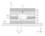
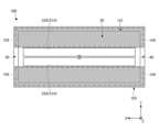
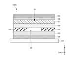
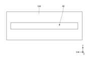
図1は、実施形態に係るRFIDタグ100の積層断面図である。図2は、図1に示すRFIDタグ100の分解斜視図である。図3は、図1に示すRFIDタグ100の上方から視た平面図である。なお、図1に示す断面図は、例えば図3に二点鎖線で示す断面線に沿ったI-I断面図である。Figure 1 is a cross-sectional view of the layers of an
RFIDタグ100は、貼付対象物200に貼付される略平面状の装置である。図1~図3に示すように、RFIDタグは、インレイ101と、磁性シート102と、誘電層103とを備える。貼付対象物200は、例えば金属である。金属としては、鉄、アルミニウム、銅などの金属の他、鉄合金、アルミ合金、銅合金等の金属の合金を含む。なお、貼付対象物200には、金属以外の他の材料、例えばプラスチックス、紙、セラミックスなども含まれる。The
実施形態に係るRFIDタグ100の主な使用用途としては、ドラム缶、H鋼等の比較的大きな金属製品への貼り付けが対象であり、これらの金属製品個々の在庫管理等を含む流通経路上の追跡(トレサビリティ)に使用できる。その他に、金属製品以外にも、本件のタグを貼り付けて使用してもよい。The main use of the
さらに、本実施形態のRFIDタグ100は、可撓性を有しており、被着体の表面が湾曲していても貼り付け可能である。湾曲状に曲げられて状態においても、良好な通信性能を発揮でき、ドラム缶やスプレー缶などの曲面を有する物品の識別にも本実施形態のRFIDタグ100を使用することができ、用途の多様化を図ることができる。Furthermore, the
インレイ101は、RFIDタグ100の機能に関する要素を含む部分であり、図2、図3に示すように、識別情報が記録されるICチップ10と、ICチップ10に接続されるスロットアンテナ20と、を有する。スロットアンテナ20は金属薄膜で形成される。スロットアンテナ20には、金属薄膜の一部が細長く切り抜かれたスロット21が設けられる。インレイ101は、例えばPETフィルム上に、アルミシートをドライラミネートで貼り付けたスロットアンテナ20が形成され、規定の位置にICチップ10が実装されている。なお、図1の断面図では、インレイ101は、PETフィルムなどの基材と、スロットアンテナ20とが纏めて一体的に図示されており、その上部にICチップ10が図示されている。The
図2、図3に示すように、インレイ101の上側の主面の中央にICチップ10が配置されている。スロットアンテナ20のスロット21は、このように配置されるICチップ10を挟んで所定方向(図2、図3の例ではX方向)に平行に延在する一対の平行部22と、これらの一対の平行部22と直交する方向(Y方向)に延在する一対の垂直部23とを有する。一対の垂直部23は、ICチップ10を挟んでX方向に略等間隔の位置にそれぞれ配置される。As shown in Figures 2 and 3, the
なお、ICチップ10のインピーダンスの周波数特性は以下のとおりである。
・866MHz:15-j265(Ω)
・915MHz:14-j252(Ω)
・953MHz:13-j242(Ω) The impedance frequency characteristics of the
・866MHz: 15-j265 (Ω)
・915MHz: 14-j252 (Ω)
・953MHz: 13-j242 (Ω)
スロットアンテナ20のインピーダンスは、915~920MHzで上記のICチップ10のインピーダンスと整合するように設計されている。このようなインピーダンスの整合により、電流の損失が少なくなり、損失を少なくすることで通信可能距離が増大する。The impedance of the
磁性シート102は、磁性材料を含有するシート材であり、インレイ101の貼付対象物200側に積層される。磁性シート102は、例えばステンレス系合金などの磁性粉末をゴム材や樹脂等に均一かつ配向して分散するように練り込んで形成される。図1~図3に示すように、磁性シート102には、磁性特性を有する磁性層を区分するスリット30が設けられる。スリット30は、磁性シート102とインレイ101とが積層された状態で、インレイ101のスロット21と重なる領域に配置される。The
スリット30は、例えば図2、図3に示すように、磁性シート102のY方向の中央の位置に、X方向に沿って延在するよう形成される。また、スロットアンテナ20のスロット21と、磁性シート102のスリット30との配置は、例えば図3に示すように、スリット30の領域にスロット21のうち少なくとも一対の平行部22の全体が含まれるように配置される。The
磁性シート102には、UHF帯の電波に対して優れた磁気シールド特性を有するものを用いるのが好ましい。磁性シート102は、磁性フィラー、バインダー樹脂等の成分が含まれる磁性塗料を、支持体上に塗布して乾燥させることで得られる。磁性シート102をUHF帯の電波に対して優れた磁気シールド特性を有するものにするためには、乾燥後の磁性シート102の膜厚が、好ましくは500μm以下、より好ましくは300μm以下となるように、磁性塗料が塗布される。また、乾燥後の磁性シート102の膜厚が、好ましくは50μm以上、より好ましくは100μm以下となるように、磁性塗料が塗布される。It is preferable to use a
同様に、磁性シート102をUHF帯の電波に対して優れた磁気シールド特性を有するものにするためには、磁性シートの860~960MHzの周波数帯域における複素比透磁率の損失係数tanδ(μ´/μ´´)は、好ましくは0.3以下、より好ましくは0.28以下である。また、磁性シートの860~960MHzの周波数帯域における複素比透磁率の損失係数tanδ(μ´/μ´´)は、好ましくは0.05以上、より好ましくは0.1以上である。Similarly, in order to provide the
なお、本実施形態におけるRFIDタグ100の全体のZ方向の厚さ(剥離紙107を除く)は、200μm~1000μmであり、好ましくは300~400μmである。また、磁性シート102とインレイ101を貼り合せた状態の厚さ(ラベル紙105及び剥離紙107は除く)は、150~250μmであり、好ましくは190~210μmであり、より好ましくは200μm程度である。ラベル紙105の厚さは、粘着剤108を含め、50μm~300μmである。剥離紙107の厚さは、50μm~300μmである。一例として、RFIDタグ100の各要素の厚さは、ラベル紙105が60μm、粘着剤108が20μm、インレイ101が48μm、粘着層104が60μm、磁性シート102が100μm、誘電層103が38μm、第2粘着層106が50μm、剥離紙107が66μmであり、RFIDタグ100の全体の厚さは442μmである。このとき、インレイ101は、例えば、厚さ38μmのPETフィルム上に、10μmのアルミシートをドライラミネートで貼り付けたスロットアンテナ20を形成し、規定の位置にICチップ10を実装することができる。In this embodiment, the overall Z-direction thickness of the RFID tag 100 (excluding the release paper 107) is 200 μm to 1000 μm, and preferably 300 to 400 μm. The thickness of the
同様に、磁性シート102をUHF帯の電波に対して優れた磁気シールド特性を有するものにするためには、磁性シートの860~960MHzの周波数帯域における複素比透磁率の実数部μ´は、好ましくは5.0以上であり、より好ましくは5.2以上である。また、磁性シートの860~960MHzの周波数帯域における複素比透磁率の実数部μ´は、好ましくは7.0以下であり、より好ましくは6.0以下である。Similarly, in order to provide the
また、上記の複素比透磁率の条件を満たすためには、磁性塗料に含まれる磁性フィラーの材質は、Fe-Cr合金であるのが好ましい。また、磁性フィラーとバインダーの固形分の質量比(磁性フィラーの質量/バインダーの固形分の質量)が70/30以上であるのが好ましく、75/25以上であるのがより好ましく、80/20以上であるのがさらに好ましい。さらに、磁性フィラーとバインダーの固形分の質量比(磁性フィラーの質量/バインダーの固形分の質量)は、95/5以下であるのが好ましく、90/10以下であるのがより好ましく、85/15以下であるのがさらに好ましい。In order to satisfy the above-mentioned conditions for complex relative permeability, the material of the magnetic filler contained in the magnetic paint is preferably an Fe-Cr alloy. The mass ratio of the magnetic filler to the solid content of the binder (mass of magnetic filler/mass of solid content of binder) is preferably 70/30 or more, more preferably 75/25 or more, and even more preferably 80/20 or more. The mass ratio of the magnetic filler to the solid content of the binder (mass of magnetic filler/mass of solid content of binder) is preferably 95/5 or less, more preferably 90/10 or less, and even more preferably 85/15 or less.
また、磁性塗料に含まれるバインダー樹脂は、エポキシ樹脂、ウレタン樹脂、またはポリエステル樹脂から成る群より選ばれる1種類以上の樹脂であり、エポキシ樹脂が好ましい。The binder resin contained in the magnetic paint is one or more resins selected from the group consisting of epoxy resins, urethane resins, and polyester resins, with epoxy resins being preferred.
誘電層103は、磁性シート102の貼付対象物200側にさらに積層され、磁性シート102と貼付対象物200との間に配置される。図2では、誘電層103は磁性シート102の下方に一体的に図示されている。誘電層103は、例えば厚紙や合成樹脂等の繊維からなる織布や不織布、セラミックガラス等の無機材料のシートなどの絶縁体で形成されるのが好ましい。本実施形態では、誘電層103は、例えば発泡PETで形成される。誘電層103の材料は、比誘電率が1.2~3.0程度であるのものが好ましく、これによりRFIDタグ100の通信距離を増やすことができる。The
また、図1に示すように、誘電層103は、インレイ101及び磁性シート102を、貼付対象物200からその厚み分だけ離間させた状態で配置させるスペーサとしても機能する。誘電層103は、外力に応じてインレイ101及び磁性シート102と共に任意に変形可能な材料で形成され、これにより貼付対象物200の貼付面が湾曲している場合でもRFIDタグ100を容易に貼付でき、汎用性を向上できるよう構成されるのが好ましい。As shown in FIG. 1, the
また、RFIDタグ100では、インレイ101と磁性シート102との間に粘着層104が配置される。粘着層104は、インレイ101と磁性シート102とを接着する。In addition, in the
図1~図3に示すように、粘着層104には、磁性シート102のスリット30と同様の第2スリット40が設けられる。第2スリット40は、磁性シート102とインレイ101とが積層された状態で、磁性シート102のスリット30と重畳配置される位置に設けられる。すなわち、第2スリット40も、スリット30と同様にインレイ101のスロット21と重なる領域に配置される。第2スリット40は、例えば図2、図3に示すように、粘着層104のY方向の中央の位置に、X方向に沿って延在するよう形成される。As shown in Figures 1 to 3, the
図1に示すように、また、図3に一点鎖線で示すように、第2スリット40のY方向の寸法は、スリット30よりやや大きいのが好ましい。つまり、第2スリット40により2つに区分される粘着層104が、磁性シート102よりY方向中央側に突出しないように設けられるのが好ましい。As shown in FIG. 1 and as shown by the dashed line in FIG. 3, it is preferable that the dimension of the
そして特に本実施形態では、磁性シート102のスリット30と、粘着層104の第2スリット40により形成される領域(図1に符号50で示す領域)は、少なくとも粘着層104より誘電率が低くなるよう形成される。より詳細には、本実施形態ではこの領域とは空隙層50であり、スリット30及び第2スリット40によってRFIDタグ100のインレイ101の直下に空隙層50が形成される。And particularly in this embodiment, the area formed by the
ここで、RFIDタグ100の積層方向(Z方向)に沿った粘着層104の厚さは、50μm以上であるのが好ましく、80μm以上であるのがさらに好ましい。また、例えば粘着層104は、比誘電率2.5以上の材料で形成されるのが好ましく、第2粘着層106の比誘電率よりも高ければ粘着層104は比誘電率2~5程度の材料で形成されてもよい。Here, the thickness of the
また、本実施形態のRFIDタグ100では、インレイ101の上方にさらにラベル紙(フィルム系タック紙)105が配置される。ラベル紙105は、Z正方向側の表面に印刷可能である。ラベル紙の素材は適宜選択可能である。ラベル紙105は、インレイ101、磁性シート102、及び誘電層103と同じ大きさで形成される。また、図1、図2に示すように、ラベル紙105のZ負方向側の裏面には粘着剤108が塗布されており、粘着剤108によりインレイ101の上面に接着されている。In the
また、本実施形態のRFIDタグ100では、貼付対象物200と対向する誘電層103の下面に粘着剤が塗布されて、第2粘着層106が形成されている。第2粘着層106は、磁性シート102の貼付対象物200側にさらに積層されており、誘電層103は、磁性シート102と第2粘着層106との間に配置される。第2粘着層106が貼付対象物200に粘着することによって、RFIDタグ100の全体が貼付対象物200に貼付される。In addition, in the
また、第2粘着層106を形成する粘着剤は、例えば長期間使用する使用環境においては接着剤を用いることができる。しかし、接着剤は硬化すると剥離が困難になる場合がある。これに対し、粘着剤は、通常、作業者の手作業等でRFIDタグ100を対象物品から剥離可能であり、さらに、粘着剤の種類によっては剥離後にRFIDタグ100を再度貼り付け可能でありRFIDタグ100として再利用可能となる場合がある。The adhesive forming the second
そして特に本実施形態では、第2粘着層106は、少なくとも粘着層104より誘電率が低い材料で形成される。粘着層104より比誘電率が低ければ、第2粘着層106の比誘電率は1~5程度が好ましく、2~3程度がより好ましい。And particularly in this embodiment, the second
また、図2に示すように、使用前のRFIDタグ100には、第2粘着層106より下方に剥離紙107が配置される。剥離紙107は、例えばインレイ101、磁性シート102、及び誘電層103より大きく形成され、インレイ101、磁性シート102、及び誘電層103の外形の全周が剥離紙107の範囲に含まれるように形成することができる。RFIDタグ100の使用時には、剥離紙107がRFIDタグ100から剥がされて、これにより露出した第2粘着層106によってRFIDタグ100が貼付対象物200に貼付される。As shown in FIG. 2, the
また、剥離紙107は、図2に例示するものよりも大きく形成され、一枚の剥離紙107の上に複数個のRFIDタグ100が配置される構成でもよい。これにより、製造効率や搬送効率を向上できる。The
なお、図2、図3に示したスロットアンテナ20のスロット21の形状は一例であり、図2、図3に示した形状には限定されない。図4は、スロットアンテナ20の他の形状のスロット21Aの一例を示す平面図である。Note that the shape of the
スロットアンテナ20のスロットの形状は、例えば図4に示すスロット21Aのように、一対の平行部22Aのみを有し、垂直部が無い形状でもよい。図4の例では、平行部22Aは、図3の垂直部23の延在方向に向けて、図3の平行部22よりも開口面積が増えており、Y方向の幅が大きくなっている。また、図4の例では、スリット30及び第2スリット40の領域にスロット21Aの一対の平行部22Aが含まれるように、スリット30及び第2スリット40の幅が広く形成されている。The shape of the slot of the
図5は、実施形態に係るRFIDタグ100の製造方法の一例を示すフローチャートである。ステップS1では、磁性特性を有する磁性層を区分するスリット30が設けられた磁性シート102(スリット入り磁性シート)が形成される。Figure 5 is a flowchart showing an example of a method for manufacturing an
このようなスリット入り磁性シート102は、例えば、ロール・トゥ・ロール方式により、ポリエステル系合成フィルム(東洋紡株式会社製、「クリスパーK1211 #38μ」)を速度3m/minで搬送しながら、該フィルム上に、コーターを用いて磁気シールド塗料によるストライプパターンを形成し、40℃から80℃まで温度を上げながら30mの硬化炉を通過させることで、形成できる。Such a slitted
ステップS2では、ステップS1にて形成されたスリット入り磁性シート102と、インレイ101とが積層される。このとき、インレイ101と磁性シート102との間には、第2スリット40が設けられた粘着層104が形成され、この粘着層104によってインレイ101と磁性シート102とが接着される。粘着層104は、例えば図1~図3に示すように第2スリット40によって2つに区分され、各部がスリット30により区分された磁性シート102のそれぞれの上に塗布される。In step S2, the slit
なお、ステップS1において磁性シート102に設けられるスリット30は、ステップS2にて磁性シート102とインレイ101とが積層された状態で、インレイ101のスロット21と重なる領域に配置されるよう形成される。同様に、ステップS2において粘着層104に設けられる第2スリット40も、ステップS2にて磁性シート102とインレイ101とが積層された状態で、インレイ101のスロット21と重なる領域に配置されるよう形成される。The
ステップS3では、磁性シート102のインレイ101と反対側の面に誘電層103が積層される。なお、ステップS2とS3とを逆に行い、磁性シート102と誘電層103とを積層した後に、インレイ101と磁性シート102とを積層する手順でもよい。In step S3, the
ステップS4では、インレイ101の磁性シート102とは反対側の面にフィルム系タック紙(ラベル紙)105が積層される。In step S4, a film-based tack paper (label paper) 105 is laminated on the side of the
このように、本実施形態に係るRFIDタグ100は、識別情報が記録されるICチップ10と、ICチップ10に接続されるスロットアンテナ20と、を有するインレイ101と、インレイ101の貼付対象物200側に積層される磁性シート102と、を備える。スロットアンテナ20は金属薄膜で形成され、スロットアンテナ20には、金属薄膜の一部が細長く切り抜かれたスロット21が設けられる。磁性シート102には、磁性特性を有する磁性層を区分するスリット30が設けられる。このスリット30は、磁性シート102とインレイ101とが積層された状態で、インレイ101のスロット21と重なる領域に配置される。As described above, the
このように磁性シート102にスリット30を設けることにより、貼付対象物200の種類によらず、RFIDタグ100のUHF帯における通信可能距離を増やすことが可能となり、通信性能を向上できる(後述する図22参照)。また、HF帯と比較して長距離通信や複数の対象物の一括読み取りが可能とUHF帯の通信可能距離を増やすことができるので、汎用性の高いRFIDタグ100を実現できる。By providing
また、貼付対象物200が金属製であると、従来のRFIDタグではタグ内のアンテナによる通信ができず、識別情報の読み出しに支障をきたすことがあるので、本実施形態に係るRFIDタグ100通信性能を向上できるという効果は、貼付対象物200が金属製であるときに特に顕著となる。In addition, if the
また、磁性シートを用いない既存の金属用のRFIDタグにおいては、被着体としての金属の影響による通信性能低下を抑えるために、インレイと被着体との間に比較的大きな間隔が必要となり、その間隔を確保するためにRFIDタグの全体の厚みが3.5mm以上であり薄型化が困難であった。In addition, existing RFID tags for metals that do not use magnetic sheets require a relatively large gap between the inlay and the adherend to prevent degradation of communication performance due to the influence of the metal used as the adherend, and in order to ensure this gap, the overall thickness of the RFID tag must be 3.5 mm or more, making it difficult to make it thinner.
これに対して、本実施形態のRFIDタグの厚みは、1mm以下であり、磁性シートを使用しない従来のRFIDタグよりも薄くすることができる。例えば、ラベル紙及び剥離紙を含んだRFIDタグの厚さとして約350μmの厚さとすることができ、金属対応のRFIDタグとして著しく薄型化ができる。In contrast, the thickness of the RFID tag of this embodiment is 1 mm or less, making it thinner than conventional RFID tags that do not use a magnetic sheet. For example, the thickness of the RFID tag including the label paper and release paper can be approximately 350 μm, making it significantly thinner than a metal-compatible RFID tag.
また、著しく薄型化が可能となることで、通常用いられている(汎用の)ラベルプリンターを用いて、ラベルの印刷とICチップへの情報の書き込みとを同時に行うことが可能で、製造効率を一層高めることができる。In addition, by making it possible to significantly reduce the thickness, it is possible to use a commonly used (general-purpose) label printer to simultaneously print the label and write information to the IC chip, further improving manufacturing efficiency.
さらに、本実施形態に係るRFIDタグ100では、インレイ101と磁性シート102との間に配置される粘着層104には、磁性シート102のスリット30と同様の第2スリット40が設けられ、第2スリット40がスリット30と重畳配置される。スリット30及び第2スリット40により形成される領域は、少なくとも粘着層104より誘電率が低くなるよう形成される。より詳細にはこの領域とは空隙層50である。Furthermore, in the
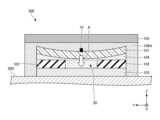
このような空隙層50をインレイ101の直下に設けることにより、RFIDタグ100の通信性能を向上でき、かつ小型化できるという効果を奏することができる。以下図6を参照してこの効果について説明する。図6は、比較例に係るRFIDタグ300の積層断面図である。図6の概略は図1と同様である。By providing such a
図6に示すRFIDタグ300は、インレイ101と磁性シート102との間に配置される粘着層104Aに、本実施形態の第2スリット40が設けられず、粘着層104Aがインレイ101や誘電層103と同様の面積で一体的に形成される点で、実施形態のRFIDタグ100と異なる。また、インレイ101とラベル紙105との間に配置される粘着剤108Aが、さらにインレイ101、磁性シート102、及び誘電層103の外周側を覆うようにZ方向にも延在し、その下端に貼付対象物200と接触するよう形成され、誘電層103の下面には粘着剤が塗布されない点でも、実施形態のRFIDタグ100と異なる。The
図6に示すように、磁性シート102にスリット30を設け、かつ、粘着層104Aに第2スリット40を設けない構成を考える。この構成では、粘着層104Aはインレイ101の下面全体に塗布されている。このため、粘着層104AのY方向中央部分が磁性シート102のスリット30の部分に進入しやすく、これにより図6に矢印Aで示すように、粘着層104Aが塗布されているインレイ101の中央部分、すなわちICチップ10が設置される部分が下方に引っ張られて湾曲しやすい傾向がある。このようなインレイ101の湾曲により、ICチップ10も磁性シート102の間のスリット30の凹みの方向に沈むので、ICチップ10が貼付対象物200の金属に接近する場合が生じ得る。As shown in FIG. 6, consider a configuration in which a
このような事象が発生すると、貼付対象物200によるインレイ101の通信性能への影響が強くなるため、RFIDタグ300の通信距離が著しく低下する。したがって、図6に示す比較例のRFIDタグ300では、通信可能距離を担保するためには、貼付対象物200によるインレイ101の通信性能への影響を予め考慮して、例えばICチップ10やスロットアンテナ20を大型化するなどの対処が必要となる。同様の対処法としては、図6に示すようインレイ101や磁性シート102などの各種タグ要素の外周部を粘着層104Aにより覆ったり、またはラベル紙105の面積をインレイ101などの各種タグ要素より大きく形成して、粘着層104Aと同様に各種タグ要素のラベル紙105によっても外周部を覆う構成とすることも考えられる。この場合、各種タグ要素を粘着層104Aやラベル紙105に内蔵する構造として、誘電層103の下面には粘着剤を塗布せずに、各種タグ要素の外周側に配置される粘着層104Aの下端によってRFIDタグ300が貼付対象物200に貼付される。これらの対処法によって、RFIDタグ300のサイズを大きくせざるを得なくなり、比較例のRFIDタグ300では小型化が難しいという問題がある。When such an event occurs, the effect of the
このような比較例の問題に対して、本実施形態のRFIDタグ100のように粘着層104に第2スリット40を設けると、図1などに示すように、インレイ101の下面のうちICチップ10が設置される中央部分には粘着剤が塗布されないので、図6を参照して説明したようにインレイ101の中央部分が下方に湾曲する事象の発生を防止できる。これにより、インレイ101のICチップ10が貼付対象物200の金属に接近することを防止できるので、貼付対象物200によるインレイ101の通信性能への影響を抑制でき、RFIDタグ100の通信可能距離の低下を防止できる。通信可能距離が低下しないため、インレイ101の大型化も不要となり、誘電層103の下面に粘着剤を塗布することも可能となるので、ラベル紙105をインレイ101などのタグ要素より大型化する必要もなくなり、RFIDタグ100の小型化を促進できる。In response to the problem of the comparative example, when the
また、ICチップ10の直下に形成される空隙層50は比誘電率が1である。すなわち、磁性シート102のスリット30と、粘着層104の第2スリット40により形成される領域である空隙層50は、少なくとも粘着層104より誘電率が低くなるよう形成される。このようにインレイ101のICチップ10と貼付対象物200との間に低誘電率の層が介在することによっても、貼付対象物200によるインレイ101の通信性能への影響を抑制でき、RFIDタグ100の通信性能を向上できる。特に、空隙層50は比誘電率が1であるので、粘着層104に対して誘電率が充分に低くなるので、貼付対象物200によるインレイ101の通信性能への影響をより一層抑制でき、RFIDタグ100の通信性能をさらに向上できる。この結果、本実施形態のRFIDタグ100は、RFIDタグ100の通信性能を向上でき、かつ小型化できる。The
また、図2、図3などに示すように、粘着層104の第2スリット40は、延在方向(X方向)の両端が粘着層104の端部まで到達して粘着層104を2つに区分するよう設けられるのが好ましい。この構成により、第2スリット40と磁性シート102のスリット30とによって形成される空隙層50は、RFIDタグ100のX方向の両端部にて第2スリット40によって開口され、この開口部を介して外部と連通することができる。これにより、空隙層50内の空気が入れ替えられるので、空隙層50の比誘電率を1に維持することが容易となる。この結果、本実施形態のRFIDタグ100は、貼付対象物200によるインレイ101の通信性能への影響をより一層抑制できるので、RFIDタグ100の通信性能を向上でき、かつ小型化できる。As shown in Figs. 2 and 3, the
さらに、RFIDタグ100の積層方向(Z方向)に沿った粘着層104の厚さは、50μm以上であるのが好ましく、80μm以上であるのがさらに好ましい。この構成により、RFIDタグ100の使用時に、インレイ101と貼付対象物200との距離を充分に確保できるので、貼付対象物200によるインレイ101の通信性能への影響をさらに抑制でき、RFIDタグ100の通信性能をさらに向上できる。これによりさらなる小型化にも繋がる。Furthermore, the thickness of the
さらに、本実施形態のRFIDタグ100では、貼付対象物200と当接して粘着する第2粘着層106は、少なくとも粘着層104より誘電率が低い材料で形成される。この構成により、低誘電率の第2粘着層106がインレイ101と金属などの貼付対象物200との間に介在するので、貼付対象物200によるインレイ101の通信性能への影響を抑制できる。この結果、本実施形態のRFIDタグ100は、RFIDタグ100の通信性能をさらに向上でき、小型化を促進できる。Furthermore, in the
また、本実施形態に係るRFIDタグ100では、磁性シート102の貼付対象物200側にさらに積層される誘電層103を備えることにより、UHF帯における通信可能距離をさらに増やすことができるので、通信性能をさらに向上できる。In addition, in the
実施形態に係るRFIDタグ100は、電磁誘導式の無線タグ、電波式の無線タグの何れにも適用可能である。特に、RFIDタグ100を、電波式の無線タグに適用した場合、リーダとの所定の無線通信距離を確保できる。所定の無線通信距離は、例えば0mから20mまでの範囲である。The
実施形態に係るRFIDタグ100は、UHF帯の電波だけでなく、VHF帯、SHF帯などの電波にも適用可能である。RFIDタグ100の使用周波数がUHF帯の周波数、例えば860~960MHz、915~925MHzなどである場合、UHF帯はVHF帯に比べて、周波数が高いため、波長が短くなり、アンテナの小型化に有利である。従って、RFIDタグ100をUHF帯の電波に好適な形状にすることで、ICチップ10の小型化を図ることができると共に、メモリ容量も小さく安価な無線タグを得ることができる。The
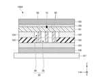
図7~図11を参照して、本実施形態の変形例を説明する。図7は、第1変形例に係るRFIDタグ100Aの積層断面図である。図8は、第2変形例に係るRFIDタグ100Bの積層断面図である。図9は、第3変形例に係るRFIDタグ100Cの積層断面図である。図7~図9の概略は図1と同様である。Modifications of this embodiment will be described with reference to Figures 7 to 11. Figure 7 is a cross-sectional view of the layers of an
上記実施形態では、磁性シート102のスリット30と、粘着層104の第2スリット40によってインレイ101の直下に空隙層50を形成する構成を例示したが、スリット30及び第2スリット40により形成される領域は、少なくとも粘着層104より誘電率が低くなるよう形成されればよく、空隙層50以外の構成でもよい。In the above embodiment, a configuration was exemplified in which the
図7に示す第1変形例100Aのように、空隙層50には、少なくとも1つ(図7の例では3本)の支持部材60が設けられる構成でもよい。支持部材60は、粘着層104と同材料、または、粘着層104より誘電率が低い材料で形成される。支持部材60は、粘着層104と同様の粘着剤でもよいし、例えば合成樹脂や木材、紙などの粘着剤以外の材料でもよいが、比誘電率が1の値により近い材料で形成するのが好ましい。As in the first modified example 100A shown in FIG. 7, the
また、支持部材60は、当該RFIDタグ100Aの積層方向(Z方向)に沿って、空隙層50中の積層方向の両端まで延在するよう形成される。すなわち、支持部材60の上端はインレイ101の下面に当接し、支持部材60の下端は誘電層103の上面に当接する。支持部材60は、例えば図7に示すように、それぞれが磁性シート102のスリット30と、粘着層104の第2スリット40の長手方向に沿ってX方向に延在する複数本を、Y方向に略等間隔で配置するストライプ状のパターンで形成することができる。なお、支持部材60のZ方向視の形状はストライプ状以外でもよく、例えば網目状やドット状などのパターンで形成してもよい。The
図8に示す第2変形例100Bのように、スリット30及び第2スリット40により形成される領域は、粘着層104より誘電率が低い材料が充填されて形成される充填層70である構成でもよい。充填層70の材料としては、粘着剤や、合成樹脂や木材、紙などの粘着剤以外の材料が挙げられる。As shown in FIG. 8, the area formed by the
図9に示す第3変形例100Cのように、粘着層104に第2スリット40を設けない構成でもよい。この構成においても、第2粘着層106が粘着層104よりも誘電率の低い材料で形成される構成によって、上記実施形態と同様に、RFIDタグ100Cの通信性能を向上でき、かつ小型化できる、という効果を奏することができる。As shown in FIG. 9, the
なお、図9に示す第3変形例100Cとは逆に、粘着層104に第2スリット40を設け、かつ、第2粘着層106が粘着層104よりも誘電率の高い材料で形成される構成としてもよい。この場合でも、磁性シート102のスリット30と、粘着層104の第2スリット40によってインレイ101の直下に形成される空隙層50によって、上記実施形態と同様に、RFIDタグ100Cの通信性能を向上でき、かつ小型化できる、という効果を奏することができる。In contrast to the third modified example 100C shown in FIG. 9, the
図10は、粘着層104の構成の第1変形例を示す平面図である。上記実施形態では、図2、図3などに示すように、粘着層104の第2スリット40は、延在方向(X方向)の両端が粘着層104の端部まで到達して粘着層104を2つに区分するよう設けられる構成を例示した。粘着層104の第2スリット40は、延在方向の少なくとも一方が粘着層104の端部まで到達するように形成されればよく、例えば図10に示すように、第2スリット40の延在方向の一方のみが粘着層104の端部まで到達し、他方は端部まで到達せずに粘着層104により塞がれる構成としてもよい。粘着層104を図10に示す構成としても、空隙層50の外部との連通箇所を一箇所設けることができるので、上記実施形態と同様に、空隙層50内の空気を入れ替えることが可能であり、空隙層50の比誘電率を1に維持することを容易にできる。10 is a plan view showing a first modified example of the configuration of the
図11は、粘着層104の構成の第2変形例を示す平面図である。図11に示すように、粘着層104の第2スリット40は、延在方向の両方が粘着層104の端部まで到達せずに粘着層104により塞がれる構成としてもよい。Figure 11 is a plan view showing a second modified example of the configuration of the
次に、本発明の実施例について具体的に説明する。Next, we will explain in detail the examples of the present invention.
<粘着層104の第2スリット40と厚さの影響>
[実施例1]
インレイ101、厚さ100μmの磁性シート102、厚さ38μmの発泡PET製の誘電層103を積層して図1に示すRFIDタグ100を作成した。インレイ101は、厚さ38μmのPETフィルム上に、10μmのアルミシートをドライラミネートで貼り付けたスロットアンテナ20を形成し、規定の位置にICチップ10を実装した。スロットアンテナ20のスロット21のアンテナパターンは、図2、図3に示す形状とした。インレイ101の上側に、厚さ20μmの粘着剤108と、厚さ60μmのラベル紙105を積層した。また、インレイ101と磁性シート102との間に厚さ60μmの粘着層104を配置し、誘電層103の下側に厚さ50μmの第2粘着層106を配置した。また、第2粘着層106の下側に厚さ66μmの剥離紙107を配置した。このように作成したRFIDタグ100の全体の厚さは442μmである。 <Effect of the
[Example 1]
The
磁性シート102は、次の手順で作成したものを用いた。まず磁性塗料は、磁性フィラーとしてFe-Cr合金(山陽特殊製鋼株式会社製、「FKTE231」)55.2質量部、バインダー樹脂としてポリエステル系ポリウレタン(荒川化学工業株式会社製、「ユリアーノ2456」、重量平均分子量30000)9.9質量部、有機溶剤としてトルエン22.6質量部、分散剤としてリン酸ポリエステル系分散剤(ビックケミージャパン株式会社製、「BYK-111」)0.4質量部、及び、消泡剤として非シリコーン系消泡剤(ビックケミージャパン株式会社製、「BYK-1752」)0.2質量部を混合して得た。次に、ロール・トゥ・ロール方式により、ポリエステル系合成フィルム(東洋紡株式会社製、「クリスパーK1211 #38μ」)を速度3m/minで搬送しながら、該フィルム上に、コーターを用いて磁気シールド塗料(上記で得られた磁性塗料)によるストライプパターンを形成し、40℃から80℃まで温度を上げながら30mの硬化炉を通過させた。これにより、スリット30入りの磁性シート102を作成した。The
磁性シート102のスリット30は、図3に示したように磁性シート102のY方向の中央を幅方向の中心位置として、Y方向の幅が25mmとなるように形成した。粘着層104の第2スリット40は、図3に示したように粘着層104のY方向の中央を幅方向の中心位置として、Y方向の幅が25mmとなるように形成した。The
インレイ101のスロットアンテナ20のサイズは、X方向の寸法を95mmとし、Y方向の寸法を40mmとした。スリット30により2つに区分される磁性シート102の寸法は、X方向を102mm、Y方向を17.5mmとした。また、第2スリット40により2つに区分される粘着層104の寸法は、X方向を102mm、Y方向を17.5mmとした。The size of the
粘着層104を形成する粘着剤には、日榮新化株式会社製の高透明基材レス両面粘着シート「MHM-FWD50」を用いた。第2粘着層106を形成する粘着剤には、新タック化成株式会社製の低誘電光学用両面粘着シートSA38xSeriesの「SA-381GF」を用いた。粘着層104の比誘電率は2.6とし、第2粘着層106の比誘電率は2.3とした。The adhesive used to form the
このように作成したRFIDタグ100を、SUS板の貼付対象物200に貼付した状態で、RFIDタグ性能検査装置(Tagformance Pro、Voyantic社製)を用いて、RFIDタグ100の周波数特性を計測した。計測時の無線通信用電波の測定周波数帯は700~1200MHzとし、EIRP(Equivalent Isotropically Radiated Power:等価等方輻射電力)は3.28Wとした。The
[実施例2]
粘着層104の厚さを80μmとしたこと以外は、実施例1と同様にRFIDタグ100を作成して、周波数特性を計測した。 [Example 2]
An
[実施例3]
空隙層50に第2粘着層106と同一の粘着剤を充填して充填層70を形成したこと以外は、実施例1と同様にRFIDタグ100を作成して、周波数特性を計測した。 [Example 3]
Except for filling the
[実施例4]
粘着層104の厚さを20μmとしたこと以外は、実施例1と同様にRFIDタグ100を作成して、周波数特性を計測した。 [Example 4]
An
[実施例5]
粘着層104の厚さを40μmとしたこと以外は、実施例1と同様にRFIDタグ100を作成して、周波数特性を計測した。 [Example 5]
An
[実施例6]
粘着層104の厚さを50μmとしたことと、粘着層104を形成する粘着剤に比誘電率が4.63のものを用いたこと以外は、実施例1と同様にRFIDタグ100を作成して、周波数特性を計測した。 [Example 6]
An
周波数特性を計測した結果、UHF帯に含まれる所定の周波数920MHzのときの通信可能距離は、実施例1では6.14m、実施例2では8m以上、実施例3では2.62m、実施例4では2.18m、実施例5では2.34m、実施例6では3.99mであった。As a result of measuring the frequency characteristics, the communication distance at a specific frequency of 920 MHz in the UHF band was 6.14 m in Example 1, 8 m or more in Example 2, 2.62 m in Example 3, 2.18 m in Example 4, 2.34 m in Example 5, and 3.99 m in Example 6.
実施例1、2、4、5、6の試験結果より、RFIDタグ100に空隙層50を設けることにより、充分な通信可能距離を確保できることが示された。同様に、実施例1、3の試験結果より、空隙層50を粘着層104より低誘電率の充填層70に置き換えた場合でも、空隙層50を設けた場合と同様の通信可能距離を確保できることが示された。The test results of Examples 1, 2, 4, 5, and 6 show that providing an
また、実施例1、2、4、5、6の試験結果より、RFIDタグ100の粘着層104の厚さを増加させるほど、通信可能距離を増やすことができ、特にUHF帯の通信可能距離を増やすことができることが示された。さらに、粘着層104の厚さが50μm以上、好ましくは80μm以上であるときに、通信可能距離の増大が顕著であることが示された。The test results for Examples 1, 2, 4, 5, and 6 also showed that the communication distance can be increased by increasing the thickness of the
<第2粘着層106の誘電率の影響>
[実施例7]
第2粘着層106を形成する粘着剤に比誘電率が3.80のものを用いたこと以外は、実施例1と同様にRFIDタグ100を作成して、周波数特性を計測した。 <Effect of Dielectric Constant of
[Example 7]
An
[実施例8]
第2粘着層106を形成する粘着剤に比誘電率が4.40のものを用いたこと以外は、実施例1と同様にRFIDタグ100を作成して、周波数特性を計測した。 [Example 8]
An
[実施例9]
第2粘着層106を形成する粘着剤に比誘電率が5.76のものを用いたこと以外は、実施例1と同様にRFIDタグ100を作成して、周波数特性を計測した。 [Example 9]
An
周波数特性を計測した結果、UHF帯に含まれる所定の周波数920MHzのときの通信可能距離は、実施例7では2.18m、実施例8では1.28m、実施例9では1.08mであった。As a result of measuring the frequency characteristics, the communication distance at a specific frequency of 920 MHz in the UHF band was 2.18 m in Example 7, 1.28 m in Example 8, and 1.08 m in Example 9.
実施例7~9の試験結果を、第2粘着層106の比誘電率以外が同一条件である実施例1と比較する。上記の実施例1の第2粘着層106の比誘電率は2.3であり、粘着層104の比誘電率2.6より小さい。一方、実施例7~9は比誘電率がすべて粘着層104のものより大きい。実施例7~9の通信可能距離は、上記の実施例1の通信可能距離よりすべて小さくなった。また、実施例7~9では、第2粘着層106の比誘電率が粘着層104のものに近くなるほど、通信可能距離が大きくなる傾向となった。したがって、実施例1、7~9の試験結果より、RFIDタグ100の第2粘着層106を、少なくとも粘着層104より誘電率が低い材料で形成することにより、貼付対象物200によるインレイ101の通信性能への影響をさらに抑制でき、RFIDタグ100の通信性能をさらに向上できることが示された。The test results of Examples 7 to 9 are compared with Example 1, which is the same except for the relative dielectric constant of the second
以上、具体例を参照しつつ本実施形態について説明した。しかし、本開示はこれらの具体例に限定されるものではない。これら具体例に、当業者が適宜設計変更を加えたものも、本開示の特徴を備えている限り、本開示の範囲に包含される。前述した各具体例が備える各要素およびその配置、条件、形状などは、例示したものに限定されるわけではなく適宜変更することができる。前述した各具体例が備える各要素は、技術的な矛盾が生じない限り、適宜組み合わせを変えることができる。The present embodiment has been described above with reference to specific examples. However, the present disclosure is not limited to these specific examples. Design modifications to these specific examples made by a person skilled in the art are also included within the scope of the present disclosure as long as they have the features of the present disclosure. The elements of each of the above-mentioned specific examples, as well as their arrangement, conditions, shape, etc., are not limited to those exemplified and can be modified as appropriate. The elements of each of the above-mentioned specific examples can be combined in different ways as appropriate, as long as no technical contradictions arise.
100、100A、100B、100C RFIDタグ
101 インレイ
10 ICチップ
20 スロットアンテナ
21 スロット
102 磁性シート
30 スリット
103 誘電層
104 粘着層
40 第2スリット
106 第2粘着層
50 空隙層
60 支持部材
70 充填層
200 貼付対象物 REFERENCE SIGNS
Claims (9)
Translated fromJapanese識別情報が記録されるICチップと、前記ICチップに接続されるスロットアンテナと、を有するインレイと、
前記インレイの前記貼付対象物側に積層される磁性シートと、
前記インレイと前記磁性シートとの間に配置される粘着層と、
を備え、
前記スロットアンテナは金属薄膜で形成され、
前記スロットアンテナには、前記金属薄膜の一部が細長く切り抜かれたスロットが設けられ、
前記磁性シートには、磁性特性を有する磁性層を区分するスリットが設けられ、
前記スリットは、前記磁性シートと前記インレイとが積層された状態で、前記インレイの前記スロットと重なる領域に配置され、
前記粘着層には、前記磁性シートの前記スリットと重畳配置される第2スリットが設けられ、
前記スリット及び前記第2スリットにより形成される領域は、少なくとも前記粘着層より誘電率が低くなるよう形成される、
RFIDタグ。 An RFID tag to be attached to an object,
An inlay having an IC chip on which identification information is recorded and a slot antenna connected to the IC chip;
A magnetic sheet is laminated on the side of the inlay that faces the object to be affixed;
an adhesive layer disposed between the inlay and the magnetic sheet;
Equipped with
The slot antenna is formed of a metal thin film,
The slot antenna is provided with a slot formed by cutting out a portion of the thin metal film,
The magnetic sheet is provided with slits that separate the magnetic layer having magnetic properties,
The slit is disposed in an area overlapping with the slot of the inlay when the magnetic sheet and the inlay are laminated together,
The adhesive layer is provided with a second slit arranged to overlap the slit of the magnetic sheet,
The region formed by the slit and the second slit is formed to have a dielectric constant lower than that of at least the adhesive layer.
RFID tag.
請求項1に記載のRFIDタグ。 The region formed by the slit and the second slit is a gap layer.
The RFID tag of claim 1 .
前記支持部材は、
前記粘着層と同材料、または、前記粘着層より誘電率が低い材料で形成され、
当該RFIDタグの積層方向に沿って前記空隙層中の前記積層方向の両端まで延在するよう形成される、
請求項2に記載のRFIDタグ。 The air gap layer is provided with at least one support member,
The support member is
The adhesive layer is formed of the same material as the adhesive layer or a material having a lower dielectric constant than the adhesive layer,
The gap layer is formed so as to extend along the stacking direction of the RFID tag to both ends in the stacking direction.
The RFID tag of claim 2.
前記空隙層は、前記第2スリットによって外部と連通する、
請求項2に記載のRFIDタグ。 The second slit in the adhesive layer is formed so that at least one of the extending directions reaches an end of the adhesive layer,
The gap layer communicates with the outside through the second slit.
The RFID tag of claim 2.
請求項1に記載のRFIDタグ。 The region formed by the slit and the second slit is a filling layer formed by being filled with a material having a dielectric constant lower than that of the adhesive layer.
The RFID tag of claim 1 .
請求項1に記載のRFIDタグ。 The thickness of the adhesive layer along the lamination direction of the RFID tag is 50 μm or more.
The RFID tag of claim 1 .
前記第2粘着層は、少なくとも前記粘着層より誘電率が低い材料で形成される、
請求項1~6のいずれか一項に記載のRFIDタグ。 A second adhesive layer is further laminated on the side of the magnetic sheet facing the object to be attached,
The second adhesive layer is formed of a material having a dielectric constant lower than that of at least the adhesive layer.
The RFID tag according to any one of claims 1 to 6.
請求項7に記載のRFIDタグ。 a dielectric layer disposed between the magnetic sheet and the second adhesive layer;
The RFID tag according to claim 7.
識別情報が記録されるICチップと、前記ICチップに接続されるスロットアンテナと、を有するインレイと、
前記インレイの前記貼付対象物側に積層される磁性シートと、
前記インレイと前記磁性シートとの間に配置される粘着層と、
前記磁性シートの貼付対象物側にさらに積層される第2粘着層と、
を備え、
前記スロットアンテナは金属薄膜で形成され、
前記スロットアンテナには、前記金属薄膜の一部が細長く切り抜かれたスロットが設けられ、
前記磁性シートには、磁性特性を有する磁性層を区分するスリットが設けられ、
前記スリットは、前記磁性シートと前記インレイとが積層された状態で、前記インレイの前記スロットと重なる領域に配置され、
前記第2粘着層は、少なくとも前記粘着層より誘電率が低い材料で形成される、
RFIDタグ。 An RFID tag to be attached to an object,
An inlay having an IC chip on which identification information is recorded and a slot antenna connected to the IC chip;
A magnetic sheet is laminated on the side of the inlay that faces the object to be affixed;
an adhesive layer disposed between the inlay and the magnetic sheet;
A second adhesive layer is further laminated on the side of the magnetic sheet facing the object to be attached;
Equipped with
The slot antenna is formed of a metal thin film,
The slot antenna is provided with a slot formed by cutting out a portion of the thin metal film,
The magnetic sheet is provided with slits that separate the magnetic layer having magnetic properties,
The slit is disposed in an area overlapping with the slot of the inlay when the magnetic sheet and the inlay are laminated together,
The second adhesive layer is formed of a material having a dielectric constant lower than that of at least the adhesive layer.
RFID tag.
Priority Applications (1)
| Application Number | Priority Date | Filing Date | Title |
|---|---|---|---|
| JP2022134730AJP7568186B2 (en) | 2022-08-26 | 2022-08-26 | RFID tags |
Applications Claiming Priority (1)
| Application Number | Priority Date | Filing Date | Title |
|---|---|---|---|
| JP2022134730AJP7568186B2 (en) | 2022-08-26 | 2022-08-26 | RFID tags |
Publications (2)
| Publication Number | Publication Date |
|---|---|
| JP2024031275A JP2024031275A (en) | 2024-03-07 |
| JP7568186B2true JP7568186B2 (en) | 2024-10-16 |
Family
ID=90105728
Family Applications (1)
| Application Number | Title | Priority Date | Filing Date |
|---|---|---|---|
| JP2022134730AActiveJP7568186B2 (en) | 2022-08-26 | 2022-08-26 | RFID tags |
Country Status (1)
| Country | Link |
|---|---|
| JP (1) | JP7568186B2 (en) |
Citations (4)
| Publication number | Priority date | Publication date | Assignee | Title |
|---|---|---|---|---|
| JP2008310540A (en) | 2007-06-14 | 2008-12-25 | Dainippon Printing Co Ltd | Non-contact IC tag having IC chip destruction prevention and communication inhibition suppression structure |
| JP2010081289A (en) | 2008-09-26 | 2010-04-08 | Mitsubishi Electric Corp | RFID tag |
| JP2021131700A (en) | 2020-02-19 | 2021-09-09 | 大王製紙株式会社 | RFID tag and antenna |
| JP2022140030A (en) | 2021-03-12 | 2022-09-26 | 大王製紙株式会社 | RFID tag and RFID tag manufacturing method |
- 2022
- 2022-08-26JPJP2022134730Apatent/JP7568186B2/enactiveActive
Patent Citations (4)
| Publication number | Priority date | Publication date | Assignee | Title |
|---|---|---|---|---|
| JP2008310540A (en) | 2007-06-14 | 2008-12-25 | Dainippon Printing Co Ltd | Non-contact IC tag having IC chip destruction prevention and communication inhibition suppression structure |
| JP2010081289A (en) | 2008-09-26 | 2010-04-08 | Mitsubishi Electric Corp | RFID tag |
| JP2021131700A (en) | 2020-02-19 | 2021-09-09 | 大王製紙株式会社 | RFID tag and antenna |
| JP2022140030A (en) | 2021-03-12 | 2022-09-26 | 大王製紙株式会社 | RFID tag and RFID tag manufacturing method |
Also Published As
| Publication number | Publication date |
|---|---|
| JP2024031275A (en) | 2024-03-07 |
Similar Documents
| Publication | Publication Date | Title |
|---|---|---|
| EP3757893B1 (en) | Antenna pattern, rfid inlay, rfid label, and rfid medium | |
| CN101142711B (en) | RFID label suitable for metal and RFID label section of the same | |
| US7501984B2 (en) | RFID tag using a surface insensitive antenna structure | |
| US8493215B2 (en) | Communication antenna, RFID tag, non-contact communication device, and non-contact communication method | |
| US20080122631A1 (en) | Multiple band / wide band radio frequency identification (rfid) tag, such as for use as a metal mount tag | |
| EP2309589A1 (en) | RFID tag using a surface intensitive antenna structure | |
| EP2365465A2 (en) | RFID tag and method of manufacturing the same | |
| CN110110833B (en) | A quarter-wave flexible UHF RFID electronic tag | |
| US12141638B2 (en) | RFID label and method of using RFID label | |
| US12299516B2 (en) | RFID tag | |
| JP7575305B2 (en) | RFID tag and method for manufacturing the same | |
| JP7568186B2 (en) | RFID tags | |
| EP1713025B1 (en) | RFID tag set and RFID tag | |
| US9508037B2 (en) | Non-contact IC label | |
| JP7014027B2 (en) | RF tag label and RF tag structure | |
| JP5061712B2 (en) | Non-contact IC tag manufacturing method | |
| JP2020071807A (en) | RF tag label and article with RF tag label | |
| JP7183651B2 (en) | RF tag label | |
| JP2012123671A (en) | Ic tag label and method for manufacturing ic tag label | |
| EP1655692A1 (en) | RF tag holding structure | |
| WO2004093246A2 (en) | Rfid tag using a surface insensitive antenna structure | |
| AU2023286508B2 (en) | Rfid label for attachment to metallic items | |
| JP7314626B2 (en) | RF tag | |
| JP5886100B2 (en) | Wireless IC tag | |
| JP7063546B2 (en) | Non-contact data transmitter / receiver |
Legal Events
| Date | Code | Title | Description |
|---|---|---|---|
| A621 | Written request for application examination | Free format text:JAPANESE INTERMEDIATE CODE: A621 Effective date:20230720 | |
| A977 | Report on retrieval | Free format text:JAPANESE INTERMEDIATE CODE: A971007 Effective date:20240717 | |
| TRDD | Decision of grant or rejection written | ||
| A01 | Written decision to grant a patent or to grant a registration (utility model) | Free format text:JAPANESE INTERMEDIATE CODE: A01 Effective date:20240903 | |
| A61 | First payment of annual fees (during grant procedure) | Free format text:JAPANESE INTERMEDIATE CODE: A61 Effective date:20240918 | |
| R150 | Certificate of patent or registration of utility model | Ref document number:7568186 Country of ref document:JP Free format text:JAPANESE INTERMEDIATE CODE: R150 |