JP7564412B2 - Dynamic learning of voltage source capabilities - Google Patents
Dynamic learning of voltage source capabilitiesDownload PDFInfo
- Publication number
- JP7564412B2 JP7564412B2JP2022193190AJP2022193190AJP7564412B2JP 7564412 B2JP7564412 B2JP 7564412B2JP 2022193190 AJP2022193190 AJP 2022193190AJP 2022193190 AJP2022193190 AJP 2022193190AJP 7564412 B2JP7564412 B2JP 7564412B2
- Authority
- JP
- Japan
- Prior art keywords
- terminal
- usb
- coupled
- voltage
- resistor
- Prior art date
- Legal status (The legal status is an assumption and is not a legal conclusion. Google has not performed a legal analysis and makes no representation as to the accuracy of the status listed.)
- Active
Links
Images


Classifications
- H—ELECTRICITY
- H02—GENERATION; CONVERSION OR DISTRIBUTION OF ELECTRIC POWER
- H02J—CIRCUIT ARRANGEMENTS OR SYSTEMS FOR SUPPLYING OR DISTRIBUTING ELECTRIC POWER; SYSTEMS FOR STORING ELECTRIC ENERGY
- H02J7/00—Circuit arrangements for charging or depolarising batteries or for supplying loads from batteries
- H02J7/007—Regulation of charging or discharging current or voltage
- H02J7/00712—Regulation of charging or discharging current or voltage the cycle being controlled or terminated in response to electric parameters
- H02J7/00714—Regulation of charging or discharging current or voltage the cycle being controlled or terminated in response to electric parameters in response to battery charging or discharging current
- H—ELECTRICITY
- H02—GENERATION; CONVERSION OR DISTRIBUTION OF ELECTRIC POWER
- H02M—APPARATUS FOR CONVERSION BETWEEN AC AND AC, BETWEEN AC AND DC, OR BETWEEN DC AND DC, AND FOR USE WITH MAINS OR SIMILAR POWER SUPPLY SYSTEMS; CONVERSION OF DC OR AC INPUT POWER INTO SURGE OUTPUT POWER; CONTROL OR REGULATION THEREOF
- H02M3/00—Conversion of DC power input into DC power output
- H02M3/22—Conversion of DC power input into DC power output with intermediate conversion into AC
- H02M3/24—Conversion of DC power input into DC power output with intermediate conversion into AC by static converters
- H02M3/28—Conversion of DC power input into DC power output with intermediate conversion into AC by static converters using discharge tubes with control electrode or semiconductor devices with control electrode to produce the intermediate AC
- H02M3/325—Conversion of DC power input into DC power output with intermediate conversion into AC by static converters using discharge tubes with control electrode or semiconductor devices with control electrode to produce the intermediate AC using devices of a triode or a transistor type requiring continuous application of a control signal
- H02M3/335—Conversion of DC power input into DC power output with intermediate conversion into AC by static converters using discharge tubes with control electrode or semiconductor devices with control electrode to produce the intermediate AC using devices of a triode or a transistor type requiring continuous application of a control signal using semiconductor devices only
- H02M3/33507—Conversion of DC power input into DC power output with intermediate conversion into AC by static converters using discharge tubes with control electrode or semiconductor devices with control electrode to produce the intermediate AC using devices of a triode or a transistor type requiring continuous application of a control signal using semiconductor devices only with automatic control of the output voltage or current, e.g. flyback converters
- G—PHYSICS
- G06—COMPUTING OR CALCULATING; COUNTING
- G06F—ELECTRIC DIGITAL DATA PROCESSING
- G06F1/00—Details not covered by groups G06F3/00 - G06F13/00 and G06F21/00
- G06F1/26—Power supply means, e.g. regulation thereof
- G06F1/266—Arrangements to supply power to external peripherals either directly from the computer or under computer control, e.g. supply of power through the communication port, computer controlled power-strips
- H—ELECTRICITY
- H02—GENERATION; CONVERSION OR DISTRIBUTION OF ELECTRIC POWER
- H02J—CIRCUIT ARRANGEMENTS OR SYSTEMS FOR SUPPLYING OR DISTRIBUTING ELECTRIC POWER; SYSTEMS FOR STORING ELECTRIC ENERGY
- H02J13/00—Circuit arrangements for providing remote indication of network conditions, e.g. an instantaneous record of the open or closed condition of each circuitbreaker in the network; Circuit arrangements for providing remote control of switching means in a power distribution network, e.g. switching in and out of current consumers by using a pulse code signal carried by the network
- H02J13/00006—Circuit arrangements for providing remote indication of network conditions, e.g. an instantaneous record of the open or closed condition of each circuitbreaker in the network; Circuit arrangements for providing remote control of switching means in a power distribution network, e.g. switching in and out of current consumers by using a pulse code signal carried by the network characterised by information or instructions transport means between the monitoring, controlling or managing units and monitored, controlled or operated power network element or electrical equipment
- H02J13/00016—Circuit arrangements for providing remote indication of network conditions, e.g. an instantaneous record of the open or closed condition of each circuitbreaker in the network; Circuit arrangements for providing remote control of switching means in a power distribution network, e.g. switching in and out of current consumers by using a pulse code signal carried by the network characterised by information or instructions transport means between the monitoring, controlling or managing units and monitored, controlled or operated power network element or electrical equipment using a wired telecommunication network or a data transmission bus
- H—ELECTRICITY
- H02—GENERATION; CONVERSION OR DISTRIBUTION OF ELECTRIC POWER
- H02J—CIRCUIT ARRANGEMENTS OR SYSTEMS FOR SUPPLYING OR DISTRIBUTING ELECTRIC POWER; SYSTEMS FOR STORING ELECTRIC ENERGY
- H02J7/00—Circuit arrangements for charging or depolarising batteries or for supplying loads from batteries
- H02J7/00032—Circuit arrangements for charging or depolarising batteries or for supplying loads from batteries characterised by data exchange
- H—ELECTRICITY
- H02—GENERATION; CONVERSION OR DISTRIBUTION OF ELECTRIC POWER
- H02M—APPARATUS FOR CONVERSION BETWEEN AC AND AC, BETWEEN AC AND DC, OR BETWEEN DC AND DC, AND FOR USE WITH MAINS OR SIMILAR POWER SUPPLY SYSTEMS; CONVERSION OF DC OR AC INPUT POWER INTO SURGE OUTPUT POWER; CONTROL OR REGULATION THEREOF
- H02M1/00—Details of apparatus for conversion
- H02M1/36—Means for starting or stopping converters
- H—ELECTRICITY
- H02—GENERATION; CONVERSION OR DISTRIBUTION OF ELECTRIC POWER
- H02M—APPARATUS FOR CONVERSION BETWEEN AC AND AC, BETWEEN AC AND DC, OR BETWEEN DC AND DC, AND FOR USE WITH MAINS OR SIMILAR POWER SUPPLY SYSTEMS; CONVERSION OF DC OR AC INPUT POWER INTO SURGE OUTPUT POWER; CONTROL OR REGULATION THEREOF
- H02M3/00—Conversion of DC power input into DC power output
- H02M3/02—Conversion of DC power input into DC power output without intermediate conversion into AC
- H02M3/04—Conversion of DC power input into DC power output without intermediate conversion into AC by static converters
- H02M3/10—Conversion of DC power input into DC power output without intermediate conversion into AC by static converters using discharge tubes with control electrode or semiconductor devices with control electrode
- H02M3/145—Conversion of DC power input into DC power output without intermediate conversion into AC by static converters using discharge tubes with control electrode or semiconductor devices with control electrode using devices of a triode or transistor type requiring continuous application of a control signal
- H02M3/155—Conversion of DC power input into DC power output without intermediate conversion into AC by static converters using discharge tubes with control electrode or semiconductor devices with control electrode using devices of a triode or transistor type requiring continuous application of a control signal using semiconductor devices only
- H02M3/156—Conversion of DC power input into DC power output without intermediate conversion into AC by static converters using discharge tubes with control electrode or semiconductor devices with control electrode using devices of a triode or transistor type requiring continuous application of a control signal using semiconductor devices only with automatic control of output voltage or current, e.g. switching regulators
- H02M3/157—Conversion of DC power input into DC power output without intermediate conversion into AC by static converters using discharge tubes with control electrode or semiconductor devices with control electrode using devices of a triode or transistor type requiring continuous application of a control signal using semiconductor devices only with automatic control of output voltage or current, e.g. switching regulators with digital control
- H—ELECTRICITY
- H04—ELECTRIC COMMUNICATION TECHNIQUE
- H04B—TRANSMISSION
- H04B3/00—Line transmission systems
- H04B3/02—Details
- H04B3/46—Monitoring; Testing
- H—ELECTRICITY
- H04—ELECTRIC COMMUNICATION TECHNIQUE
- H04B—TRANSMISSION
- H04B3/00—Line transmission systems
- H04B3/54—Systems for transmission via power distribution lines
- H—ELECTRICITY
- H02—GENERATION; CONVERSION OR DISTRIBUTION OF ELECTRIC POWER
- H02J—CIRCUIT ARRANGEMENTS OR SYSTEMS FOR SUPPLYING OR DISTRIBUTING ELECTRIC POWER; SYSTEMS FOR STORING ELECTRIC ENERGY
- H02J7/00—Circuit arrangements for charging or depolarising batteries or for supplying loads from batteries
- H—ELECTRICITY
- H02—GENERATION; CONVERSION OR DISTRIBUTION OF ELECTRIC POWER
- H02M—APPARATUS FOR CONVERSION BETWEEN AC AND AC, BETWEEN AC AND DC, OR BETWEEN DC AND DC, AND FOR USE WITH MAINS OR SIMILAR POWER SUPPLY SYSTEMS; CONVERSION OF DC OR AC INPUT POWER INTO SURGE OUTPUT POWER; CONTROL OR REGULATION THEREOF
- H02M1/00—Details of apparatus for conversion
- H02M1/0003—Details of control, feedback or regulation circuits
- H—ELECTRICITY
- H02—GENERATION; CONVERSION OR DISTRIBUTION OF ELECTRIC POWER
- H02M—APPARATUS FOR CONVERSION BETWEEN AC AND AC, BETWEEN AC AND DC, OR BETWEEN DC AND DC, AND FOR USE WITH MAINS OR SIMILAR POWER SUPPLY SYSTEMS; CONVERSION OF DC OR AC INPUT POWER INTO SURGE OUTPUT POWER; CONTROL OR REGULATION THEREOF
- H02M3/00—Conversion of DC power input into DC power output
- H02M3/22—Conversion of DC power input into DC power output with intermediate conversion into AC
- H02M3/24—Conversion of DC power input into DC power output with intermediate conversion into AC by static converters
- H02M3/28—Conversion of DC power input into DC power output with intermediate conversion into AC by static converters using discharge tubes with control electrode or semiconductor devices with control electrode to produce the intermediate AC
- H02M3/325—Conversion of DC power input into DC power output with intermediate conversion into AC by static converters using discharge tubes with control electrode or semiconductor devices with control electrode to produce the intermediate AC using devices of a triode or a transistor type requiring continuous application of a control signal
- H02M3/335—Conversion of DC power input into DC power output with intermediate conversion into AC by static converters using discharge tubes with control electrode or semiconductor devices with control electrode to produce the intermediate AC using devices of a triode or a transistor type requiring continuous application of a control signal using semiconductor devices only
- H02M3/33507—Conversion of DC power input into DC power output with intermediate conversion into AC by static converters using discharge tubes with control electrode or semiconductor devices with control electrode to produce the intermediate AC using devices of a triode or a transistor type requiring continuous application of a control signal using semiconductor devices only with automatic control of the output voltage or current, e.g. flyback converters
- H02M3/33515—Conversion of DC power input into DC power output with intermediate conversion into AC by static converters using discharge tubes with control electrode or semiconductor devices with control electrode to produce the intermediate AC using devices of a triode or a transistor type requiring continuous application of a control signal using semiconductor devices only with automatic control of the output voltage or current, e.g. flyback converters with digital control
Landscapes
- Engineering & Computer Science (AREA)
- Power Engineering (AREA)
- General Engineering & Computer Science (AREA)
- Theoretical Computer Science (AREA)
- Computer Networks & Wireless Communication (AREA)
- Computer Hardware Design (AREA)
- Physics & Mathematics (AREA)
- General Physics & Mathematics (AREA)
- Signal Processing (AREA)
- Power Sources (AREA)
- Direct Current Feeding And Distribution (AREA)
Description
Translated fromJapanese相互接続規格には、第1のデバイスが、第2のデバイスへの電力搬送能力(例えば、電圧及び電流)を通告する電力搬送プロトコルを定義するものがある。したがって、第1のデバイスは電力の供給源であり、第2のデバイスは電力を引き込む。いくつかの実装において、ソースデバイスの電力能力は、ソースデバイス内部のコントローラにおいてハードコード化される。ソースデバイスは、事前設定された構成にアクセスし、それらの特定の電力能力をシンクデバイスに通告する。シンクは通告された電力能力のうちの1つを選択し、ソースデバイスは合致した電力能力について電力ソースを構成する。Some interconnect standards define a power transfer protocol where a first device advertises its power transfer capabilities (e.g., voltage and current) to a second device. Thus, the first device is the source of power and the second device draws power. In some implementations, the power capabilities of the source device are hard-coded in a controller inside the source device. The source device accesses a pre-configured configuration and advertises their specific power capabilities to the sink device. The sink selects one of the advertised power capabilities and the source device configures the power source for the matching power capability.
一実施形態において、システムが、電源出力ノード上で複数の出力電圧の任意のものを生成するように構成可能な電源を含み得る。このシステムは、電源に結合される電圧自動検出電力分配(PD)コントローラも含み得る。電圧自動検出PDコントローラは、ケーブルを介してシステムに結合されるデバイスの存在を検出するため入力信号を監視し、複数の制御信号の組み合わせをアサートするように構成され得る。制御信号の各組み合わせについて、電圧自動検出PDコントローラは、電源からの出力電圧の値を測定し得、測定した値をストアし得、デバイスへの伝送のために複数のパケットを生成し得る。各パケットは、測定された出力電圧を示すパラメータを含む。In one embodiment, a system may include a power supply configurable to generate any of a number of output voltages on a power supply output node. The system may also include a voltage auto-sensing power distribution (PD) controller coupled to the power supply. The voltage auto-sensing PD controller may be configured to monitor input signals to detect the presence of a device coupled to the system via a cable and to assert a combination of a number of control signals. For each combination of control signals, the voltage auto-sensing PD controller may measure a value of an output voltage from the power supply, store the measured value, and generate a number of packets for transmission to the device. Each packet may include a parameter indicative of the measured output voltage.
別の実施形態において、システムが、電源、電力スイッチ、電圧自動検出電力分配(PD)コントローラ、及び、構成可能抵抗器ディバイダネットワークを含み得る。電源は、電源出力ノード上に複数の出力電圧の任意のものを生成するように構成可能であり得る。電力スイッチは、電源出力ノードと電圧バスとの間に結合され得、電源出力ノードから電圧バスへ出力電圧を結合するように構成され得る。電圧自動検出PDコントローラは、電源に、及び、イネーブル信号を介して電力スイッチに、結合され得る。電圧自動検出PDコントローラは、電力スイッチが選択的に開状態又は閉状態となるように制御するように構成され得る。構成可能抵抗器ディバイダネットワークは、電圧自動検出PDコントローラに結合され得る。電圧自動検出PDコントローラは、ケーブルを介してシステムに結合されるシンクデバイスの検出の際に、電源出力電圧学習モードを始動するように構成され得る。電源出力電圧学習モードの間、電圧自動検出PDコントローラは、電力スイッチをオフ状態にするように構成するためにイネーブル信号を用い、構成可能抵抗器ディバイダネットワークへの複数の制御信号の組み合わせをアサートするように構成され得る。制御信号の各組み合わせについて、電圧自動検出PDコントローラは、電源からの出力電圧の値を測定し、シンクデバイスへの伝送のために複数のパケットを生成するように構成され得、各パケットは測定された出力電圧を示すパラメータを含む。In another embodiment, a system may include a power supply, a power switch, a voltage auto-sensing power distribution (PD) controller, and a configurable resistor divider network. The power supply may be configurable to generate any of a plurality of output voltages on a power supply output node. The power switch may be coupled between the power supply output node and a voltage bus and may be configured to couple the output voltage from the power supply output node to the voltage bus. The voltage auto-sensing PD controller may be coupled to the power supply and to the power switch via an enable signal. The voltage auto-sensing PD controller may be configured to control the power switch to be selectively open or closed. The configurable resistor divider network may be coupled to the voltage auto-sensing PD controller. The voltage auto-sensing PD controller may be configured to initiate a power supply output voltage learning mode upon detection of a sink device coupled to the system via a cable. During the power supply output voltage learning mode, the voltage auto-sensing PD controller may be configured to assert a combination of a plurality of control signals to the configurable resistor divider network using an enable signal to configure the power switch to an off state. For each combination of control signals, the voltage auto-sensing PD controller may be configured to measure the value of the output voltage from the power source and generate a number of packets for transmission to the sink device, each packet including a parameter indicative of the measured output voltage.
更に別の実施形態において、或る方法が、第1のデバイスの第2のデバイスへの取付けを検出すること、及び、複数の出力電圧を生成するために第2のデバイスの電源を反復的に構成することを含み得る。各反復について、この方法は、各出力電圧を測定すること、及び、各測定された出力電圧を示す値をストアすることを含み得る。この方法は、通信パケットを第1のデバイスに伝送することも含み得る。通信パケットは、測定された出力電圧を示す値を含み得る。In yet another embodiment, a method may include detecting attachment of a first device to a second device and iteratively configuring a power supply of the second device to generate multiple output voltages. For each iteration, the method may include measuring each output voltage and storing a value indicative of each measured output voltage. The method may also include transmitting a communication packet to the first device. The communication packet may include a value indicative of the measured output voltage.
次に、様々な例の詳細な説明のために添付の図面を参照する。Reference is now made to the accompanying drawings for a detailed description of the various examples.
本明細書では、ユニバーサルシリアルバス(USB)電力搬送(PD)及びタイプC規格に言及する場合があるが、こうした言及は単に例示の目的であり、本開示及び特許請求の範囲の範囲を限定するものではない。本開示は、他の規格も対象としている。様々なUSB PD及びタイプC規格が、USBケーブル及びコネクタを介したより高い電力レベルの搬送を可能にする。この技術は、例えば5Vより多くを必要とし得る、ラップトップ、タブレットなどのためのユニバーサル電力プラグをつくる。USB-PD規格は、例えば、USB-PDケーブルを介して接続されるポート間の通信リンクを定義する。通信は、半二重及びパケットベースであり得る。通信パケットは、ソースポートがポートに提供する電圧及び電流を、これら2つのポートに通信及び交渉させ得る情報を含む。USB PD規格による基礎となる通信は、二位相マーク符号化(BMC)であり得る。こうした通信は、異なるワイヤ上ではあるが同じケーブルを通過する通常のUSB通信とは独立して成される。USB-PD通信パケットは、USBデータ導体ではなく異なる導体(例えば、制御チャネル(CC)導体)を介して流れる。Although references may be made herein to Universal Serial Bus (USB) Power Delivery (PD) and Type-C standards, such references are for illustrative purposes only and do not limit the scope of the present disclosure and claims. Other standards are also contemplated by the present disclosure. Various USB PD and Type-C standards allow for the delivery of higher power levels over USB cables and connectors. This technology creates a universal power plug for laptops, tablets, etc., that may require more than 5V, for example. The USB-PD standard defines a communication link between ports connected, for example, via a USB-PD cable. The communication may be half-duplex and packet-based. The communication packets contain information that allows the two ports to communicate and negotiate the voltage and current that the source port provides to the port. The underlying communication with the USB PD standard may be bi-phase mark coding (BMC). Such communication is independent of the normal USB communication, which runs over the same cable, but on a different wire. USB-PD communication packets flow over different conductors (e.g., control channel (CC) conductors) rather than USB data conductors.
電力ソースデバイス(時には「ソース」と呼ばれる)が、ソース能力メッセージ(Source Capabilities message)と呼ばれるUSB PDメッセージに含まれる電力データオブジェクト(PDO)の形態で、その供給タイプを通告し得る。固定供給(Fixed Supply)PDOは、電圧及び最大電流を含み、可変供給(Variable-Supply)PDOは、最大電圧、最小電圧、及び最大電流を含み、バッテリ供給(Battery-Supply)PDOは、最大電圧、最小電圧、及び最大電力を含む。ソースデバイスが、複数の固有のPDOを通告し得る。シンクデバイス(「シンク」と呼ばれることもある)が、要求(Request)メッセージと呼ばれるUSB PDメッセージを介して、通告された電力能力のうちの1つを要求し得る。ソースがシンクの要求を満たし得る場合、ソースは受け入れ(Accept)メッセージを送信し、要求を満たし得ない場合、ソースは拒否又は待機(Reject or Wait)メッセージを送信し得る。ソースがその電源を調節すると、ソースは、同意されたレベルでの電力の引き込みをシンクが開始し得る旨をシンクに通知するために、PS_RDYメッセージ
を送信する。 A power source device (sometimes called a "source") may advertise its supply type in the form of a Power Data Object (PDO) contained in a USB PD message called the Source Capabilities message. A Fixed-Supply PDO contains voltage and maximum current, a Variable-Supply PDO contains maximum voltage, minimum voltage, and maximum current, and a Battery-Supply PDO contains maximum voltage, minimum voltage, and maximum power. A source device may advertise multiple unique PDOs. A sink device (sometimes called a "sink") may request one of the advertised power capabilities via a USB PD message called a Request message. If the source can meet the sink's request it sends an Accept message, if not it may send a Reject or Wait message. Once the source has adjusted its power it sends a PS_RDY message to inform the sink that it may begin drawing power at the agreed upon level.
その電圧能力を通告する前に、ソースはまず、シンクがケーブル又は他の接続メカニズムを用いて取り付けられていることを検出する。ソースは、CC導体上にプルアップ抵抗器を含み得る。シンクは、CC導体上にプルダウン抵抗器又はクランプを含む。ソースは、CC導体上のDC電圧を測定することによって、シンクの存在を検出する。1つの電圧レベル又は電圧のレンジにおいて、ソースはシンクが取り付けられていないと判定し、異なるレベル又は電圧のレンジにおいて、ソースはシンクが取り付けられていると判定する。次いで、ソースは、CC導体上の電圧がデバウンスの目的で所定の時間期間の間(例えば、100ms~200ms)安定することを検証し得る。適用可能な規格について、ソースは、次いで、所定の電圧(例えば、5V)を475ms内のケーブルの電力ワイヤ(USB PD規格において、電圧バス(VBUS)と呼ばれる)に印加する。所定の電圧(例えば、5V)を印加した後、ソースは、いずれの電圧が提供可能であるか、及び各対応する電圧についての電流レベルなどの、そのソース電力能力を(例えば、前述のようなPDOを用いて)通告する通信メッセージを送信し得る。 Before advertising its voltage capabilities, the source first detects that a sink is attached using a cable or other connection mechanism. The source may include a pull-up resistor on the CC conductor. The sink includes a pull-down resistor or clamp on the CC conductor. The source detects the presence of a sink by measuring the DC voltage on the CC conductor. At one voltage level or range of voltages, the source determines that a sink is not attached, and at a different level or range of voltages, the source determines that a sink is attached. The source may then verify that the voltage on the CC conductor stabilizes for a predetermined period of time (e.g., 100 ms to 200 ms) for debounce purposes. For applicable standards, the source then applies a predetermined voltage (e.g., 5V) to the cable's power wire (called the voltage bus (VBUS ) in the USB PD standard) within 475 ms. After applying a predetermined voltage (e.g., 5V), the source may send a communication message (e.g., using a PDO as described above) advertising its source power capabilities, such as which voltages it can provide and the current levels for each corresponding voltage.
電源出力電圧学習モードにおいて、ソースは、ソースがシンクに電圧を通告し得る前に、ソースの電源が生成し得る電圧を決定する。開示する実施形態によれば、ソースにおける電圧自動検出PDコントローラが、こうした電力能力をシンクに通告する前にソースの電源が生成し得る電圧を動的に学習する。本実施形態において、電源の電力能力は、ソースのPDコントローラ内に事前に構成されない。代わりに、電源の電力分配能力は、ソースにおける電圧自動検出PDコントローラによって動的に決定される。最小及び最大電圧によって特徴付けられる(及び、単に複数の離散電圧レベルではない)供給タイプの場合、電圧自動検出PDコントローラは、電源をその最大及び最小電圧に達するように個別に制御し得、その後、電圧レンジを通告する。単一電圧によって特徴付けられる供給タイプの場合、電源は複数の電圧設定を有し、その任意のものが用いられ得る。この場合、自動検出PDコントローラは、電源がその固有電圧の各々に達するように制御し、またその後、それらの固有の電圧を通告する。In a power supply output voltage learning mode, the source determines the voltages that the source's power supply can generate before the source can advertise the voltage to the sink. According to a disclosed embodiment, a voltage auto-detecting PD controller at the source dynamically learns the voltages that the source's power supply can generate before advertising such power capabilities to the sink. In this embodiment, the power capabilities of the power supply are not pre-configured in the PD controller at the source. Instead, the power distribution capabilities of the power supply are dynamically determined by the voltage auto-detecting PD controller at the source. For supply types characterized by minimum and maximum voltages (and not simply multiple discrete voltage levels), the voltage auto-detecting PD controller can individually control the power supply to reach its maximum and minimum voltages and then advertise a voltage range. For supply types characterized by a single voltage, the power supply has multiple voltage settings, any of which can be used. In this case, the auto-detecting PD controller controls the power supply to reach each of its unique voltages and then advertises those unique voltages.
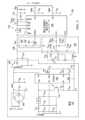
図1は、ケーブル90を介してシンクデバイス80に結合される電力ソースデバイス100の実施形態を示す。電力ソースデバイス100は、動作電圧及び電流を生成し得、これらをシンクデバイス80に提供可能であり、シンクデバイス80は電力ソースデバイス100によって提供された電圧及び電流を用いて、シンクデバイスにおける負荷82に電力供給する。負荷82は、プロセッサ、メモリ、カスタム回路、受動構成要素、能動構成要素などの、任意のタイプの回路を含み得る。いくつかの実施形態において、電力ソースデバイス100は、ACメイン電力をシンクデバイス80のためのDC電圧及び電流に変換する電力アダプタである、電力「ブリック」を含み得る。他の実施形態において、電力ソースデバイス100は、コンピュータ、タブレットデバイスなどの計算デバイスであり得るか、又はその一部であり得る。更に、電力ソースデバイス100は、デュアルモード動作、すなわち、電力を生成するソースデバイスか、又は別のデバイスによって生成される電力を引き込むシンクデバイスのいずれかとして、動作し得る。いくつかの実装形態の場合、電力ソース及びシンクデバイス100及び80は、USB PD及びタイプC規格を実装するが、他の規格及びプロトコルも同様に実装され得る。FIG. 1 illustrates an embodiment of a
電力ソースデバイス100は、電源102、出力キャパシタ(COUT)、プルアップ抵抗器106(これは、電力ソースデバイスの集積回路に集積される電流ソースとして実装され得る)、及び、電圧自動検出電力分配(PD)コントローラ120を含む。電源102は、入力ACメイン電圧を受け取り、1つ又はそれ以上の出力DC電圧及び電流に変換し、電圧バス(VBUS)110を介して出力DC電力をシンクデバイス80に提供する。電力ソースデバイス100の電圧自動検出PDコントローラ120は、電源102がいずれの電圧レベルを生成し、シンクデバイス80に提供するかを交渉するために、シンクデバイス80におけるPDコントローラ84(これは、電圧自動検出PDコントローラ120と同じであってもよく又は異なっていてもよい)と相互作用し得る。電源102は、複数の異なるレベルのいずれかにおける出力電圧(例えば、5V、9V、15V、20Vなど)を生成することが可能であり得る。様々な実施形態において、電源102は、単一の出力電圧のみ、2つの異なる出力電圧、3つの出力電圧などを生成することが可能であり得る。ソースデバイスにおける電圧自動検出PDコントローラ120は、(例えば、制御チャネル(CC)導体(例えば、ワイヤ、導電性トレースなど)104を介して伝送されるメッセージによって)シンクデバイス80におけるPDコントローラ84に通告する。シンクデバイス80は、通告された電圧のうちの1つを選択可能であり、電圧自動検出PDコントローラ120は、同意電圧をシンクデバイス80に供給するように電源102を構成することによって応答する。最小電圧と最大電圧との間の電圧レンジ能力によって電源が特徴付けられる実施形態において、シンクデバイス80は、電圧自動検出PDコントローラ120によって通告される最小と最大との間の電圧を要求し得る。 The
CC導体104は、電力交渉プロセスの間に通信パケットを伝送するために用いられることに加えて、シンクデバイス80が、例えばケーブル90を介して電力ソースデバイス100に接続されているときを検出し得るという付加的な理由のために用いられ得る。プルアップ抵抗器106は、電力ソースデバイス100内のCC導体104に結合され、プルダウン抵抗器86はシンクデバイス80内のCC導体104に結合される。そのため、電力ソースデバイス100にシンクデバイス80が接続されていない状態では、CC導体上の電圧レベルは、プルダウン抵抗器86を伴うシンクデバイス80がケーブル90を介して電力ソースデバイスに接続されている場合よりも高いレベルとなる。したがって、電圧自動検出PDコントローラ120は、CC導体104上の電圧レベルを監視することによって、シンクデバイス80が電圧自動検出PDコントローラ120に接続されているかどうかを検出し得る。In addition to being used to transmit communication packets during the power negotiation process, the
前述のように、電源102は、いくつかの異なる電圧の任意のものを生成することが可能であり得る。開示する実施形態によれば、電圧自動検出PDコントローラ120は、コントローラが、電源102の特定の電圧能力を動的に決定し、それら特定の電圧をシンクデバイス80に通告するプロセスを実施する。そのため、電圧自動検出PDコントローラ120は、特定の電圧セットについて事前構成される必要はなく、したがって、多様な電源と共に用いられ得る。また、電圧自動検出PDコントローラ120は電源102が生成し得る実際の電圧を学習するので、電源102は特定の精密な電圧レベルについて設計する必要はない。すなわち、電源システムを設計するとき、実際の各電源は、その出力電圧をわずかに異なるものにし得る異なる特徴を有し得るが、電圧自動検出PDコントローラ120は電源が実際に生成し得る電圧を測定するので、電源設計のために設計の制限及び許容範囲が緩和され得る。As mentioned above, the
図2は、電力ソースデバイス100の可能な実装の例を示す。ソースデバイス100は、電源102を形成するために、図示されるように共に結合される様々な構成要素を含む。構成要素のうちのいくつかは、ブリッジ整流器140、隔離変圧器144、及び定電圧定電流フライバックコントローラ142を含み得る。抵抗器、キャパシタなどの様々な他の受動構成要素も同様に示されている。ブリッジ整流器140は、入力するACメイン波形を整流する。フライバックコントローラ142は、フォトダイオード111及び光検出器114によって形成される光結合器を用いて定電圧を提供する。Figure 2 shows an example of a possible implementation of
電圧自動検出PDコントローラ120は、CC1及びCC2と標示される1対のCC端子を有するものとして示されている。ケーブル90のためのコネクタは対称的であり得、コネクタが固定されておらず、したがって2つの向きのいずれかに接続され得ることを意味する。このように、2つのCC導体が存在し得、ケーブルが取り付けられている向きに応じて1つが用いられる。電源102は、VOUTとして図2に示され、ノード108上の電圧である出力電圧を生成する。ノード108は、電源102の出力ノードであり、電力スイッチ(例えば、電界効果トランジスタQ1)116に結合する。電力スイッチ116は、電圧自動検出PDコントローラ120からの制御信号GDenによって、オン(閉)状態又はオフ(開)状態であるように制御され得る。ノード110は、電力スイッチ116のノード108とは反対側の端子に結合し、そのノード上の電圧は、電圧バス(VBUS)に提供され、ケーブル90を介してシンクデバイス80に提供される。電力スイッチ116がオンであるとき、VBUS上の電圧は、VOUT電圧と概ね同じである。 The voltage auto-
電圧自動検出PDコントローラ120は、VOUT又はVBUS電圧のいずれか又は両方をデジタル形式に変換するために用いられ得るアナログデジタルコンバータ(ADC)を含み得る。図示されるように、VOUT電圧は、VPWR端子経由で電圧自動検出PDコントローラ120に提供され、VBUS電圧はVPWR端子に提供される。 Voltage auto-
構成可能抵抗器ディバイダネットワーク130も含まれ得、電圧自動検出PDコントローラ120に結合され得る。図2の実施形態において、構成可能抵抗器ディバイダネットワーク130は、VOUTノード108と接地との間に結合される1対の直列接続抵抗器を含み得る。図示されるように、抵抗器は、抵抗器112a(RFBU)及び抵抗器112b(RFBL)を含む。抵抗器112aと112bとの間のノードは、抵抗器ノード117と示される。電圧自動検出PDコントローラ120は、CTL1及びCTL2として図示される(及び、CTL1信号及びCTL2信号と呼ばれることもある)1対の制御端子を含む。構成可能抵抗器ディバイダネットワーク130はまた、電圧自動検出PDコントローラ120のCTL1端子に結合される抵抗器112c(RFBL1)、及びCTL2端子に結合される抵抗器112d(RFBL2)を含む。CTL1及びCTL2端子は、オープン・ドレイン端子であり得る。そのため、電圧自動検出PDコントローラ120は、CTL1及びCTL2の端子の各々を、開であるか又は接地されているように構成し得る。CTL1端子が低に下げられた場合、その対応する抵抗器112cは抵抗器112bと並列に結合され、それによって、抵抗器ディバイダネットワーク130の一部の抵抗を変化させる。しかしながら、CTL2が開のままである場合、抵抗器112cは浮遊のままであり、したがって事実上、抵抗器ディバイダネットワークに含まれない。CTL2端子についても同様であり、CTL2を低に下げることで、その対応する抵抗器112dは抵抗器112bと並列に配置されることになり、低に下げられない場合、抵抗器112dは抵抗器112bと並列に配置されない。制御信号CTL1及びCTL2の各組み合わせは、構成可能抵抗器ディバイダネットワークを制御信号の他の組み合わせとは異なって構成し得る。他の実施形態において、電力ソースデバイス100は、構成可能抵抗器ディバイダネットワークではなく、抵抗器112aを介して制御された様式で電流の量を変動させるためのプログラム可能な電流源を含み得る。他の実施形態において、自動検出PDコントローラは、例えばデジタルアナログコンバータ(DAC)を用いて、異なる基準電圧を設定することが可能な回路を有し得る。 A configurable
電流は、VOUTから構成可能抵抗器ディバイダネットワーク130を介して接地へと流れる。電流の大きさは、抵抗器ディバイダネットワーク130の等価抵抗の関数であり、したがって、CTL1及びCTL2の信号の動作によって、抵抗器112c及び112dの各々が抵抗器112bと並列に結合されるかどうかの関数である。CTL1及びCTL2の信号の動作に起因して、抵抗器ディバイダネットワーク130を介する電流の量を変動させることによって、抵抗器112aの電圧は変動し得、したがって、フォトダイオード111を介する電流は変動し得る。フォトダイオード111によって生成される光の強度は、フォトダイオードを介する電流の関数である。フォトダイオード111によって生成される光は、光検出器114によって検出される。したがって、フォトダイオード111及び光検出器114の組み合わせは、フライバックコンバータ142への光フィードバック信号を形成する。フライバックコンバータ142は、光フィードバック信号を用いてその出力電圧VOUTをレギュレートする。 Current flows from VOUT through configurable
電源102は、複数の異なる電圧を生成することが可能であり得、こうした各電圧について、フォトダイオード111からの光フィードバック信号に基づいて特定の電圧を追跡するようにVOUTをレギュレートする。また、電源102は、特定の出力電圧VOUTを生成するために、CTL1信号及びCTL2信号の構成を介して、電圧自動検出PDコントローラ120によって構成され得る。この例における2つの制御信号(CTL1及びCTL2)の場合、構成可能抵抗器ディバイダネットワーク130について4つの構成が可能である。4つの組み合わせは、抵抗器112c及び112dが抵抗器112bと並列に含まれるかどうかに関する限り、互いに異なる。
開示される実施形態によれば、シンクデバイス80を(例えば、CC1又はCC2導体上の電圧レベルを監視することによって)検出すると、電圧自動検出PDコントローラ120は、電源102が生成し得る様々な電圧を識別するプロセスを開始する。電圧自動検出PDコントローラ120は、CTL1及びCTL2の信号の様々な組み合わせを周期的に繰り返すことによって、このプロセスを行い得る。CTL1及びCTL2の制御信号の各組み合わせについて、電圧自動検出PDコントローラ120は、その出力電圧VOUTの値を測定し、測定された値を(例えば、コントローラ内部の、又は他の方式でコントローラにアクセス可能な、不揮発性メモリ内に)ストアする。電圧自動検出PDコントローラ120は、例えば電圧自動検出PDコントローラ120内部のADCを用いて測定を行う前に、VOUT電圧を整定させることができるようにするために、所定の期間の間待機し得る。CTL1及びCTL2の様々な組み合わせを周期的に繰り返した後、電圧自動検出PDコントローラ120は、前述のように、測定された電圧をシンクデバイス80に通告し得る。例えば、電圧自動検出PDコントローラ120は、シンクデバイス80に伝送するための複数のパケットを生成し得、各パケットは測定された出力電圧を示すパラメータを含む。プログラム可能電流源を伴うようないくつかの実施形態において、自動検出PDコントローラが妥当な時間内に測定するには多過ぎる電圧が存在し得、こうした実施形態におけるコントローラは、最大及び最小の電圧を測定し得、最大及び最小の電圧をシンクデバイスに通告し得る。 According to disclosed embodiments, upon detecting sink device 80 (e.g., by monitoring the voltage level on the CC1 or CC2 conductor), voltage auto-detecting
電圧自動検出PDコントローラ120がVOUT学習プロセスを行なっている間、電力スイッチ116は、電圧自動検出PDコントローラ120によってオフ状態になるように構成され得る。したがって、前述の学習プロセスの間に電源によって生成される様々な電圧は、VBUSノード110に与えられず、したがってシンクデバイス80に提供されない。電圧自動検出PDコントローラ120によって測定される電圧は、電力スイッチ116がオフ(開)状態にある際のVOUTノード108上の電圧である。 While the voltage auto-
しかしながら、いくつかの実装形態において、電力ソースデバイス100は、シンクデバイス80の存在を検出する際に、事前に設定された時間内にVBUSノード110上に所定の電圧をかけるように義務付けられ得る。例えば、USB PD規格の場合、電力ソースデバイス100は、シンクデバイス80の検出の475ms内にVBUSに5Vをかけるものである。したがって、図2の実施形態の場合、様々なCTL1及びCTL2の組み合わせを周期的に繰り返し、VOUT電圧を測定及び記録するために必要な時間は、USB PD規格に従って475ms未満とすべきである。このタイミング要件を満たすための他の実施形態を下記で説明する。 However, in some implementations,
図1の実施形態は、VOUTノード108と接地との間に結合される負荷回路140も含む。この例における負荷回路140は、ソリッドステートスイッチ144と直列に結合される抵抗器142を含む。ソリッドステートスイッチ144のゲートは、負荷回路140のためのイネーブル/ディセーブル端子として機能する。ソリッドステートスイッチ144のゲートは、電圧自動検出PDコントローラ120からの放電(DSCG1)信号によって駆動され得る。DSCG1信号が1つの論理状態(例えば、高)にある場合、スイッチ144はオン(閉)状態にあり、それによってVOUTノード108からの電流が接地に流れるようにし得る。DSCG1にとって反対の論理状態にある場合、スイッチ144はオフ(開)状態にあることになり、それによって電流がVOUTノード108から接地へと流れないようにする。電圧自動検出PDコントローラ120は、DSCG1信号を用いて、VOUTノード108に負荷を効率的に印加し、電源出力を安定させるのを助けることができる。いくつかの実施形態において、負荷回路140が図1に示されるように電圧自動検出PDコントローラ120から分離され得、又は、ソリッドステートスイッチ144が電圧自動検出PDコントローラ120に統合され得る。電圧自動検出PDコントローラ120は、電流がVBUSノード110から抵抗器119を介して、及び内部ソリッドステートスイッチを介して、接地へと流れることができるように構成可能な、放電信号DSCG2も含む。したがって、電圧自動検出PDコントローラ120は、VOUTノード108及びVBUSノード110のいずれか又は両方に、負荷を印加するように構成可能である。 The embodiment of FIG. 1 also includes a
電源102が生成し得る様々なVOUT電圧を測定する際、電圧自動検出PDコントローラ120は、測定される各電圧について上限及び下限の電圧も計算し得る。したがって、こうした電圧は電源の出力電圧の許容レンジを定義し、したがって、電圧不足及び過電圧の保護を実装するために用いることができる。いくつかの実施形態において、電圧自動検出PDコントローラ120は、電圧の上限及び下限閾値を以下のように計算し、
VUPPER=VMEAS×αUPPER+OUPPER
VLOWER=VMEAS×αLOWER+OLOWER
上記式で、VUPPERは上限電圧であり、VMEASは測定された電圧であり、αUPPER、αLOWER、OUPPER、及びOLOWERは、認められる供給許容範囲及び認められる測定許容範囲を含む。αUPPER、αLOWER、OUPPER、及びOLOWERパラメータは、先験的に決定され得、電圧自動検出PDコントローラ120のメモリにストアされ得る。電源102によって生成され得る、電圧自動検出PDコントローラ120によって決定される可能な各VOUT電圧について、電圧自動検出PDコントローラ120は、電圧の上限及び下限閾値の対を計算し、計算された閾値をメモリにストアする。動作の間、電圧自動検出PDコントローラ120はVBUS上の電圧を測定し、電圧不足又は過電圧状態が検出された場合、それに応じて(例えば、電力スイッチ116をオフにすることによって)その電圧を、適用可能な電源電圧についての閾値と比較し得る。 In measuring the variousVOUT voltages that the
VUPPER =VMEAS ×αUPPER +OUPPER
VLOWER =VMEAS ×αLOWER +OLOWER
In the above equation, VUPPER is the upper limit voltage, VMEAS is the measured voltage, and αUPPER , αLOWER , OUPPER , and OLOWER comprise the allowed supply tolerances and the allowed measurement tolerances. The αUPPER , αLOWER , OUPPER , and OLOWER parameters may be determined a priori and stored in a memory of voltage auto-
デバイス100が別のデバイスに電力を供給するように機能するか、又は別のデバイスから電力を引き込むように機能するかのいずれかが可能であり得る実施形態において、電力ソースデバイス100の電圧自動検出PDコントローラ120は、デバイス100が(電圧を生成するのではなく)ケーブル80を介して他のデバイスから動作電圧を受け取るように構成される「シンク」モードに、それ自体を初期化し得る。しかしながら、シンクモードの間、デバイス100(現在、電力を引き込むように動作している)の電圧自動検出PDコントローラ120は、制御信号CTL1及びCTL2の様々な組み合わせをアサートするため、及び、それ自身の電源からの出力電圧値を測定するために、前述のプロセスを行い得る。その後、電圧自動検出PDコントローラ120は、測定された電圧を通告するために、PR_SWAPメッセージと呼ばれるUSB PDメッセージを他のデバイスに送信し得る。この技法により、デバイス100は、様々な起こり得る電圧を測定するための時間をより多く有し得る。In an embodiment in which
別の実施形態において、電圧自動検出PDコントローラ120は或る値までVOUT電圧を測定し得るが、測定した値を異なる値に丸め得る。例えば、電圧自動検出PDコントローラは、VOUTを14.8Vとして測定し得るが、測定した値を15Vまでに丸めて、測定した14.8Vの値ではなく15Vをシンクデバイス80に通告する。こうした実施形態において、電力ソースデバイス100によって生成され、シンクデバイス80に通信されるパケットは、実際の測定された電圧値と丸められた値との組み合わせを含み得る。いずれにしても、電圧自動検出PDコントローラ120はパケットをシンクデバイス80に送信し、パケットは、測定されたVOUT電圧値を示すパラメータを含み、パラメータは、実際の測定された値又はその丸められた値のいずれかである。 In another embodiment, voltage auto-
図3は、電圧自動検出PDコントローラ120の少なくとも一部のブロック図を図示する。この例において、電圧自動検出PDコントローラ120は、状態機械150、電圧マルチプレクサ152、及びADC154を含む。ADC154は、VOUT電圧又はVBUS電圧のいずれかを、状態機械150からの制御信号によってマルチプレクサ152を介して選択されたものとしてデジタル化するために用いられ得る。状態機械150は、機械命令を実行するマイクロコントローラ、プログラム可能論理デバイス、又は他の適切なタイプの制御回路として実装され得る。状態機械150は、前述のような電圧閾値を計算するため、並びに、測定された電圧値及び/又は丸められた値をストアするために用いられる、パラメータをストアするためのメモリ152を含むか又はメモリ152に結合し得る。 3 illustrates a block diagram of at least a portion of the voltage auto-
図4は、電力ソースデバイス100の別の実施形態を示す。この実施形態における電源102及び電圧自動検出PDコントローラ120は、図2に関連して上述したものと概ね同じである。しかしながら、図4には、図2とのいくつかの相違点が存在する。図2の構成可能抵抗器ディバイダネットワーク130は、図4において、構成可能抵抗器ディバイダネットワーク170に置き換えられている。構成可能抵抗器ディバイダネットワーク130と同様に、構成可能抵抗器ディバイダネットワーク170は、VOUTノード108と接地との間に結合される直列に接続される抵抗器172及び174の対を含む。別の対の抵抗器176及び178が、抵抗器172と174との間に画定されるノード173に接続される。抵抗器172及び174の対向する端子を電圧自動検出PDコントローラのCTL及びCTL2端子に接続するのではなく、抵抗器172、174は、対応するソリッドステートスイッチを介して接地に結合される。したがって、抵抗器176は抵抗器ノード173とスイッチ180との間を接続し、抵抗器178は抵抗器ノード173とスイッチ182との間を接続する。CTL1信号及びCTL2信号は、スイッチ180及び182のゲートに提供され、したがって、それらスイッチをオン及びオフにし得る。所与のスイッチ180、182がオンであるとき、その対応する抵抗器176、178は抵抗器174に並列に結合され、オンでないとき、その対応物は浮遊のままであるため、抵抗器174に並列に結合されない。 FIG. 4 illustrates another embodiment of the
図2の実施形態に対する図4の実施形態についての別の相違点は、図4の実施形態がDC‐DC(DC/DC)コンバータ160を含む点である。DC/DCコンバータ160は、電源102とVBUSノード110との間に結合される。したがって、DC/DCコンバータ160への入力DC電圧はVOUT電圧であり、DC/DCコンバータ160からの出力DC電圧はVBUSノード110に提供される。DC/DCコンバータ160からの出力電圧は、電力ソースデバイスが、対応する規格の時間期間内にVBUSノード110に課する電圧であり得る。上記のUSB PDの例において、電力ソースデバイス100は、475ms内にVBUSに5Vをかけるものであった。したがって、DC/DCコンバータ160によって生成される出力電圧は、この例では5Vであり得る。DC/DCコンバータ160は、電圧自動検出PDコントローラ120の制御端子に結合されるイネーブル/ディセーブル端子も含む(例えば、図4においてDCDCenと図示される)。DCDCen信号は、DC/DCコンバータ160の動作をイネーブル又はディセーブルするために、電圧自動検出PDコントローラ120によって選択的にアサートされ得る。電源によって生成可能な様々な可能な電圧を順序付けし、電圧を測定し、それらをメモリにストアするプロセスが、電源が必要な電圧(例えば、5V)を生成するように構成されなければならない割り当てられた時間期間よりも長くかかる実施形態において、電圧自動検出PDコントローラ120は、DC/DCコンバータ160がその出力電圧を生成すること、及び/又はその出力電圧をVBUSノード110上に提供することを可能にし得る。DC/DCコンバータ160は、電源102によって生成し得る様々な電圧の任意のものから、所定の電圧(この例では5V)を生成することが可能であり得る。したがって、DC/DCコンバータ160の許容入力電圧範囲は、少なくとも、電源102が生成し得ると考えられる様々な電圧を含むだけの十分な広さである。いくつかの実施形態において、DC/DCコンバータ160がVBUSに電圧を印加する間、自動検出PDコントローラ120は5Vをシンクデバイス80に通告するのみであり、少量の電流を与えるのみである。このような場合、DC/DCコンバータ160は、相対的にシンプルで安価な回路として実装され得る。 Another difference for the embodiment of FIG. 4 relative to the embodiment of FIG. 2 is that the embodiment of FIG. 4 includes a DC-to-DC (DC/DC)
DC/DCコンバータ160は、電圧自動検出PDコントローラ120によって、VBUSノード110のための出力電圧を生成することを可能にし得、これは電力スイッチ116がオフの間に行われ、電圧自動検出PDコントローラ120は、電源102が生成し得る様々な電圧を学習するプロセスを続行し得る。 The DC/
図5は、図1と同様の実施形態を示す。図5は、ソースデバイスの電圧自動検出PDコントローラに、電源102によって生成可能な様々な電圧を測定及び記録するためのより多くの時間を提供するための技法を図示する。この例において、スイッチ180をオフにすることによって、ケーブルのソースデバイス側のCC導体104からプルアップ抵抗器106が取り外され得る。スイッチ180は、電圧自動検出PDコントローラ120からの制御信号によって制御され得る。スイッチ180をオフにし、回路からプルアップ抵抗器を効率的に取り外すことで、シンクデバイス80の切断をエミュレートする。電圧自動検出PDコントローラ120は、電源電圧を学習するプロセスを実施し得、その後、スイッチ180をオンにし得る。Figure 5 shows an embodiment similar to Figure 1. Figure 5 illustrates a technique for providing the source device's voltage auto-sensing PD controller more time to measure and record the various voltages that can be generated by the
図6は、開示される実施形態に従った方法20のフローチャートを示す。動作は図示された順で、又は異なる順で成され得る。また、動作は順次成され得るか、或いは、2つ又はそれ以上の動作が同時に成され得る。FIG. 6 illustrates a flow chart of a method 20 in accordance with a disclosed embodiment. The actions may be performed in the order shown, or in a different order. Additionally, the actions may be performed sequentially, or two or more actions may be performed simultaneously.
202において、方法は、電力ソースデバイス100を低電力状態に初期化することを含む。この状態の間、電力ソースデバイス(及び、例えば、特に電圧自動検出PDコントローラ)は電源出力電圧学習モードで動作し、このモードにおいて、実施される少なくとも1つの機能が、シンクデバイス80の取付けまで待機し、これを監視し、図6に示される動作の残りを実施する。いくつかの実施形態において、電圧自動検出PDコントローラ120は、CC導体(CC1又はCC2)上の電圧を所定の電圧レンジと比較することによってこの動作を実施し得、この場合、1つの電圧レンジが、シンクデバイス80が取り付けられていないことを示し得、別の電圧レンジが、シンクデバイスの取付けを示し得る。204において、方法はシンクデバイスの取付けを検出することを含む。At 202, the method includes initializing the
206において、方法は取り付けられたシンクデバイスの有効化を開始する。取り付けられたシンクデバイスの有効化は、シンクデバイスが実際に取り付けられていないときの誤アラームを防ぐために、CC導体上の電圧が所定の時間期間の間、下限閾値と上限閾値との間にとどまっていることを保証することを含み得る。いくつかの実施形態において、下限閾値は0ボルトである。しかしながら、一例において、下限閾値及び上限閾値はそれぞれ0.2V及び1.6Vであり、所定の時間期間は150msである。所定の時間期間は、必要とされる時間期間内でVBUSへの電圧がイネーブルである限り、所望に応じて長くすることが可能である。 At 206, the method begins enabling the attached sink device. Enabling the attached sink device may include ensuring that the voltage on the CC conductor remains between a lower threshold and an upper threshold for a predetermined period of time to prevent false alarms when the sink device is not actually attached. In some embodiments, the lower threshold is 0 volts. However, in one example, the lower and upper thresholds are 0.2V and 1.6V, respectively, and the predetermined period of time is 150 ms. The predetermined period of time can be as long as desired, so long as the voltage to the VBUS is enabled within the required period of time.
動作208~214は反復ループを記述し、この反復ループにおいて、電力ソースデバイスの電圧自動検出PDコントローラ120が、電源が生成し得る様々な電圧を学習する。208において、方法は、電源に第1の出力電圧(VOUT)を生成させるために電圧自動検出PDコントローラ120を設定することを含む。いくつかの実施形態において、電圧自動検出PDコントローラは制御信号CTL1及びCTL2を調節し得、それによって、前述のような光フィードバック信号に基づく特定の出力電圧を電源に生成させ得る。210において、方法は、電源からの出力電圧(VOUT)を(212において)測定する前に、特定の時間期間の間待機することを含み得る。この時間期間は、より正確な電圧測定が成されるように、電源の出力電圧を安定化できるようにする助けとなり得る。いくつかの実施形態において、時間期間は、固定され、電圧自動検出PDコントローラ120内に構成される。他の実施形態において、時間期間は連続測定に基づき得る。すなわち、電源が出力電圧のために構成された後、一連の電圧測定を立て続けに(例えば、1ms間隔で)行い得、また、測定された電圧がこうした1つの測定から次の測定へと閾値量よりも多く変化するのを中止する(例えば、1つの測定から後続の測定への変化が閾値割合未満である)とき、一連の測定は中止され、最後の測定電圧が用いられる。また、212において、測定された電圧は、例えば、電圧自動検出PDコントローラ120の内部メモリにストアされ得る。記録は、測定された電圧を電源に生成させるために用いられたCTL1及びCTL2の信号のための構成設定も含み得る。また、電圧自動検出PDコントローラ120は、(前述の例において説明したような)測定された電圧についての上限及び下限電圧閾値も計算し得、計算した電圧閾値をメモリにもストアし得る。このように、CTL1/CTL2信号の所与の構成について測定された電圧の、並びに、対応する上限及び下限電圧閾値の、記録がメモリにおいてつくられる。いくつかの実施形態において、記録は不揮発性メモリに対して行われ得るため、シンクデバイスを取り付けるごとに学習プロセスを実施する必要はない。他の実施形態において、自動検出PDコントローラ120は、ACメイン電力入力が取り外されるまで記録をストアし得る。 Operations 208-214 describe an iterative loop in which the power source device's voltage auto-
214において、電圧自動検出PDコントローラ120は、CTL1/CTL2について、用いるべきそれ以上の構成が残っているかどうかを判定する。こうした組み合わせのいずれかが残っている場合、216において、電圧自動検出PDコントローラ120はそれに応じてCTL1及びCTL2を制御し、方法は動作210へとループバックする。いくつかの実施形態において、適用可能な規格(例えば、USB PD規格)について、電源は所定の電圧(例えば、5V)を生成することが可能でなければならない。その電圧が必要であるため、電圧自動検出PDコントローラ120は、その電圧を測定するためにCTL1、CTL2を用いて電源を使用する必要はない。代わりに、電圧自動検出PDコントローラ120は、電源102がその電圧を生成し得ることを先験的に知っている。いくつかの実施形態において、必要な電圧(例えば、5V)は、電源によって生成可能な最低電圧であり得、CTL1及びCTL2の信号の特定の組み合わせ(例えば、両方の信号が高であり、ドレインは開のまま)に対応する。CTL1/CTL2信号の特定の組み合わせは、所望の場合、電源出力電圧学習プロセスの間、省かれ得る。いくつかの実施形態において、複数の電圧を生成することが知られている所定のCTL1、CTL2信号を有し得る、複数の電圧を実装し得る。At 214, the voltage auto-
電圧自動検出PDコントローラ120は、CTL1及びCTL2信号のすべての関連する組み合わせを介して電源102を使用した場合、次に218において、方法は、上記で説明したように、取り付けたシンクデバイス80の有効化を完了することを含む。シンク有効化プロセスを完了するために、CC電圧は、或る時間量の間、閾値間に留まるべきであり、この時間量は、206で用いられる時間に比べて相対的に長くし得る。206においてタイマが開始され得、CC電圧が安定化したことを保証するためにより多くの時間が必要とされる場合、218においてタイマが延長され得る。介在する動作208~216が、取り付けられたシンクデバイスが有効化されている所定の時間期間の間、実施され得る。有効なシンクデバイスが取り付けられていない(220において決定される)場合、プロセスは202へとループバックし、プロセスは反復し得る。しかしながら、有効なシンクデバイスが取り付けられている場合、電源102は、所定の出力電圧(例えば、5V)を生成するように(CTL1及びCTL2信号の適切な組み合わせを介して)構成され、電力スイッチ116は、所定の電圧をVBUSノード110に提供するために、電圧自動検出PDコントローラ120によってオンにされる。電力スイッチは、上記で説明したように、電圧自動検出PDコントローラ120からの制御信号を介してオンにされる。 If the voltage auto-
224において、電圧自動検出PDコントローラ120は、パケットを生成し、シンクデバイスに伝送して、電源によって生成可能であるものと決定された様々な電圧を通告する。前述のように、通告内容は、測定された実際の電圧又は測定された電圧の丸められたバージョンを含み得る。At 224, the voltage auto-
本願における説明及び特許請求の範囲全体を通じて、或る用語が特定のシステム構成要素を言及するために用いられる。当業者であれば理解されるように、異なる会社が或る構成要素を異なる名前によって言及し得る。本願は、名前は異なるが機能は異ならない構成要素を区別することを意図していない。本願の考察及び特許請求の範囲において、「含む(including)」及び「含有する(comprising)」は、非限定形式で用いられており、そのため、「含むが限定されない」ことを意味するものと解釈されるべきである。また、「結合する」という用語は、間接的又は直接的な有線又はワイヤレス(例えば、光)接続のいずれかを意味するものと意図されている。したがって、第1のデバイスが第2のデバイスに結合する場合、その接続は、直接的な接続を介するか、又は他のデバイス及び接続を介する間接的な接続を介するものであり得る。上記の考察は、本発明の原理及び様々な実施形態を例示するためのものである。当業者であれば、上記開示を完全に理解すれば、多数の変形及び改変が明らかとなろう。下記の特許請求の範囲は、こうしたすべての変形及び改変を包含するものと解釈されることが意図される。Throughout the description and claims of this application, certain terms are used to refer to specific system components. As one skilled in the art will appreciate, different companies may refer to a component by different names. This application does not intend to distinguish between components that differ in name but not function. In the discussion and claims of this application, "including" and "comprising" are used in an open-ended manner and should therefore be interpreted to mean "including but not limited to." Additionally, the term "couple" is intended to mean either an indirect or direct wired or wireless (e.g., optical) connection. Thus, when a first device couples to a second device, the connection may be through a direct connection or through an indirect connection via other devices and connections. The above discussion is intended to illustrate the principles and various embodiments of the present invention. Numerous variations and modifications will become apparent to one skilled in the art once the above disclosure is fully appreciated. It is intended that the following claims be interpreted to embrace all such variations and modifications.
Claims (12)
Translated fromJapanese前記USBケーブルの電圧バス(VBUS)導体に結合されるように適応されるVBUS端子と、
前記USBケーブルの構成チャネル(CC)導体に結合されるように適応されるCC端子と、
前記VBUS端子に結合される電圧出力(VOUT)ノードであって、電源に結合されるように適応される、前記VOUTノードと、
前記VBUS端子と前記CC端子と前記VOUTノードとに結合されるコントローラ回路と、
前記コントローラ回路の放電信号接続と前記VOUTノードとに結合される負荷回路と、
抵抗器分圧器であって、
第1の端子と前記コントローラ回路に結合される第2の端子とを有する第1の抵抗器と、
前記第1の抵抗器の第1の端子に結合される第3の端子と前記コントローラ回路に結合される第4の端子とを有する第2の抵抗器と、
前記VOUTノードに結合される第5の端子と前記第1の抵抗器の第1の端子に結合される第6の端子とを有する第3の抵抗器と、
前記第1の抵抗器の第1の端子に結合される第7の端子と前記電源に結合されるように適応される第8の端子とを有する第4の抵抗器と、
を含む、前記抵抗器分圧器と、
を含む、USBソースデバイス。 1. A Universal Serial Bus (USB) source device adapted to be coupled to a USB sink device via a USB cable, comprising:
a voltage bus (VBUS ) terminal adapted to be coupled to a VBUS conductor of the USB cable;
a component channel (CC) terminal adapted to be coupled to a CC conductor of the USB cable;
a voltage output (VOUT ) node coupled to the VBUS terminal, the VOUT node adapted to be coupled to a power supply;
a controller circuit coupled to the VBUS terminal, the CC terminal, and the VOUT node;
a load circuit coupled to a discharge signal connection of the controller circuit and to theVOUT node;
A resistor voltage divider comprising:
a first resistor having a first terminal and a second terminal coupled to the controller circuit;
a second resistor having a third terminal coupled to the first terminal of the first resistor and a fourth terminal coupled to the controller circuit;
a third resistor having a fifth terminal coupled totheVOUTnode and a sixth terminal coupled to the first terminal of the first resistor;
a fourth resistor havinga seventh terminal coupled to the first terminal of the first resistor and an eighth terminal adapted to be coupled to the power source;
the resistor dividerincluding :
2. A USB source device including:
前記コントローラ回路が、前記USBケーブルを介して前記USBシンクデバイスと供給容量を通信する前に前記電源の供給容量を決定するように構成される、USBソースデバイス。 2. The USB source device of claim 1,
The USB source device, wherein the controller circuit is configured to determine a supply capacity of the power source prior to communicating the supply capacity with the USB sink device over the USB cable.
前記供給容量が、5Vと9Vと15Vと20Vとの少なくとも1つの電圧レベルを含む、USBソースデバイス。 3. A USB source device according to claim 2, comprising:
The USB source device, wherein the supply capacity includes at least one of the following voltage levels: 5V, 9V, 15V, and 20V.
前記負荷回路が、
前記VOUTノードに結合される第1の端子と第2の端子とを有する抵抗器と、
前記コントローラ回路に結合される制御端子と前記抵抗器の第2の端子に結合される第1の電流端子と接地に結合される第2の電流端子とを有するトランジスタと、
を含む、USBソースデバイス。 2. The USB source device of claim 1,
The load circuit is
a resistor having a first terminal and a second terminal coupled to theVOUT node;
a transistor having a control terminal coupled to the controller circuit, a first current terminal coupled to the second terminal of the resistor, and a second current terminal coupled to ground;
2. A USB source device including:
前記コントローラ回路が、
前記CC端子を介して前記USBシンクデバイスを検出し、
前記CC端子を介してデータパケットを前記USBシンクデバイスに送信する、
ように構成される、USBソースデバイス。 2. The USB source device of claim 1,
The controller circuitry comprises:
Detecting the USB sink device via the CC terminal;
Transmitting a data packet to the USB sink device via the CC terminal;
A USB source device configured to:
前記コントローラ回路が、
前記CC端子を介して前記USBシンクデバイスを検出し、
前記USBシンクデバイスが検出された後に前記VBUS端子を前記電源に結合する、
ように構成される、USBソースデバイス。 2. The USB source device of claim 1,
The controller circuitry comprises:
Detecting the USB sink device via the CC terminal;
coupling the VBUS terminal to the power supply after the USB sink device is detected;
A USB source device configured to:
前記USBケーブルの電圧バス(VBUS)導体に結合されるように適応されるVBUS端子と、
前記USBケーブルの構成チャネル(CC)導体に結合されるように適応されるCC端子と、
前記VBUS端子に結合される電圧出力(VOUT)ノードであって、電源に結合されるように適応される、前記VOUTノードと、
前記VBUS端子と前記CC端子と前記VOUTノードとに結合されるコントローラ回路と、
前記VOUTノードに結合される第1の入力と前記コントローラ回路に結合される第2の入力と前記VBUS端子に結合される出力とを有するDC・DCコンバータと、
前記VOUTノードと前記コントローラ回路とに結合される抵抗器分圧器であって、前記電源に結合されるように適応される、前記抵抗器分圧器と、
を含む、USBソースデバイス。 1. A Universal Serial Bus (USB) source device adapted to be coupled to a USB sink device via a USB cable, comprising:
a voltage bus (VBUS ) terminal adapted to be coupled to a VBUS conductor of the USB cable;
a component channel (CC) terminal adapted to be coupled to a CC conductor of the USB cable;
a voltage output (VOUT ) node coupled to the VBUS terminal, the VOUT node adapted to be coupled to a power supply;
a controller circuit coupled to the VBUS terminal, the CC terminal, and the VOUT node;
a DC to DC converter having a first input coupled to theVOUT node, a second input coupled to the controller circuit, and an output coupled tothe VBUS terminal;
a resistor divider coupled to theVOUT node and to the controller circuit, the resistor divider adapted to be coupled to the power supply;
2. A USB source device including:
前記コントローラ回路が、前記USBケーブルを介して前記USBシンクデバイスと供給容量を通信する前に前記電源の供給容量を決定するように構成される、USBソースデバイス。 8. A USB source device according to claim7 , comprising:
The USB source device, wherein the controller circuit is configured to determine a supply capacity of the power source prior to communicating the supply capacity with the USB sink device over the USB cable.
前記供給容量が、5Vと9Vと15Vと20Vとの少なくとも1つの電圧レベルを含む、USBソースデバイス。 9. A USB source device according to claim8 , comprising:
The USB source device, wherein the supply capacity includes at least one of the following voltage levels: 5V, 9V, 15V, and 20V.
前記抵抗器分圧器が、
前記コントローラ回路に結合される第1の制御端子と第1の電流端子と第2の電流端子とを有する第1のトランジスタと、
前記コントローラ回路に結合される第2の制御端子と第3の電流端子と第4の電流端子とを有する第2のトランジスタと、
前記VOUTノードに結合される第1の端子と第2の端子とを有する第1の抵抗器と、
前記第1の抵抗器の第2の端子に結合される第3の端子と前記第1のトランジスタの第1の電流端子に結合される第4の端子とを有する第2の抵抗器と、
前記第1の抵抗器の第2の端子に結合される第5の端子と前記第2のトランジスタの第3の電流端子に結合される第6の端子とを有する第3の抵抗器と、
前記第1の抵抗器の第2の端子に結合される第7の端子と前記電源に結合されるように適応される第8の端子とを有する第4の抵抗器と、
を含む、USBソースデバイス。 8. A USB source device according to claim7 , comprising:
The resistor divider comprises:
a first transistor having a first control terminal coupled to the controller circuit, a first current terminal, and a second current terminal;
a second transistor having a second control terminal coupled to the controller circuit, a third current terminal, and a fourth current terminal;
a first resistor having a first terminal coupled to theVOUT node and a second terminal;
a second resistor having a third terminal coupled to the second terminal of the first resistor and a fourth terminal coupled to the first current terminal of the first transistor;
a third resistor having a fifth terminal coupled to the second terminal of the first resistor and a sixth terminal coupled to a third current terminal of the second transistor;
afourth resistor having a seventh terminal coupled to the second terminal of the first resistor and an eighth terminal adapted to be coupled to the power source;
2. A USB source device including:
前記コントローラ回路が、
前記CC端子を介して前記USBシンクデバイスを検出し、
前記CC端子を介してデータパケットを前記USBシンクデバイスに送信する、
ように構成される、USBソースデバイス。 8. A USB source device according to claim7 , comprising:
The controller circuitry comprises:
Detecting the USB sink device via the CC terminal;
Transmitting a data packet to the USB sink device via the CC terminal;
A USB source device configured to:
前記コントローラ回路が、
前記CC端子を介して前記USBシンクデバイスを検出し、
前記USBシンクデバイスが検出された後に前記VBUS端子を前記電源に結合する、
ように構成される、USBソースデバイス。 8. A USB source device according to claim7 , comprising:
The controller circuitry comprises:
Detecting the USB sink device via the CC terminal;
coupling the VBUS terminal to the power supply after the USB sink device is detected;
A USB source device configured to:
Applications Claiming Priority (4)
| Application Number | Priority Date | Filing Date | Title |
|---|---|---|---|
| US15/392,047US10476394B2 (en) | 2016-12-28 | 2016-12-28 | Dynamic learning of voltage source capabilities |
| US15/392,047 | 2016-12-28 | ||
| PCT/US2017/068650WO2018125969A1 (en) | 2016-12-28 | 2017-12-28 | Dynamic learning of voltage source capabilities |
| JP2019535873AJP7189876B2 (en) | 2016-12-28 | 2017-12-28 | Dynamic learning of voltage source capability |
Related Parent Applications (1)
| Application Number | Title | Priority Date | Filing Date |
|---|---|---|---|
| JP2019535873ADivisionJP7189876B2 (en) | 2016-12-28 | 2017-12-28 | Dynamic learning of voltage source capability |
Publications (2)
| Publication Number | Publication Date |
|---|---|
| JP2023039959A JP2023039959A (en) | 2023-03-22 |
| JP7564412B2true JP7564412B2 (en) | 2024-10-09 |
Family
ID=62625146
Family Applications (2)
| Application Number | Title | Priority Date | Filing Date |
|---|---|---|---|
| JP2019535873AActiveJP7189876B2 (en) | 2016-12-28 | 2017-12-28 | Dynamic learning of voltage source capability |
| JP2022193190AActiveJP7564412B2 (en) | 2016-12-28 | 2022-12-02 | Dynamic learning of voltage source capabilities |
Family Applications Before (1)
| Application Number | Title | Priority Date | Filing Date |
|---|---|---|---|
| JP2019535873AActiveJP7189876B2 (en) | 2016-12-28 | 2017-12-28 | Dynamic learning of voltage source capability |
Country Status (5)
| Country | Link |
|---|---|
| US (3) | US10476394B2 (en) |
| EP (1) | EP3563517B1 (en) |
| JP (2) | JP7189876B2 (en) |
| CN (3) | CN120414785A (en) |
| WO (1) | WO2018125969A1 (en) |
Families Citing this family (23)
| Publication number | Priority date | Publication date | Assignee | Title |
|---|---|---|---|---|
| EP3282550B1 (en)* | 2016-02-05 | 2020-04-15 | Guangdong Oppo Mobile Telecommunications Corp., Ltd. | Adapter and charging control method |
| JP6730888B2 (en)* | 2016-09-05 | 2020-07-29 | キヤノン株式会社 | Electronic device and control method thereof |
| US10476394B2 (en)* | 2016-12-28 | 2019-11-12 | Texas Instruments Incorporated | Dynamic learning of voltage source capabilities |
| JP6878102B2 (en)* | 2017-04-07 | 2021-05-26 | キヤノン株式会社 | Electronic devices and their control methods |
| FR3070554A1 (en)* | 2017-08-25 | 2019-03-01 | Stmicroelectronics (Grenoble 2) Sas | METHOD AND DEVICE FOR REDUCING THE POWER SUPPLY VOLTAGE OF A TYPE C USB RECEIVER DEVICE SUPPORTING THE USB POWER DELIVERY MODE |
| US11018576B2 (en) | 2017-08-25 | 2021-05-25 | Stmicroelectronics (Grenoble 2) Sas | Method and device for decreasing the power supply voltage of a c-type USB receiver device supporting a USB power delivery mode |
| KR102358562B1 (en) | 2017-09-12 | 2022-02-04 | 삼성전자주식회사 | Device and method for detecting conditions generating leakage current in usb interface |
| US11398740B2 (en)* | 2018-04-06 | 2022-07-26 | Stmicroelectronics (Grenoble 2) Sas | Method for selecting a supply source power |
| US11152807B2 (en)* | 2018-04-06 | 2021-10-19 | Stmicroelectronics (Grenoble 2) Sas | Method for selecting a supply source power |
| WO2020024116A1 (en)* | 2018-07-31 | 2020-02-06 | 华为技术有限公司 | Interface configuration method, terminal device and interface |
| KR102714346B1 (en)* | 2018-09-03 | 2024-10-10 | 삼성전자주식회사 | Method for identifying an external electronic device based on power information, storage medium and an electronic device therefor |
| GB201815161D0 (en)* | 2018-09-18 | 2018-10-31 | Oe Electrics Ltd | Modular power and socket assembly |
| US10948958B2 (en)* | 2018-10-05 | 2021-03-16 | Dell Products L.P. | System and method of utilizing power supply units |
| WO2020129303A1 (en) | 2018-12-19 | 2020-06-25 | パナソニックIpマネジメント株式会社 | Image-capturing apparatus |
| JP6645669B1 (en)* | 2019-01-21 | 2020-02-14 | Necプラットフォームズ株式会社 | Interface circuit, information processing device, display method, and program |
| CN112311028B (en)* | 2019-07-29 | 2023-01-17 | 瑞昱半导体股份有限公司 | Method for selecting a power supply option for a USB powered device |
| KR102770637B1 (en) | 2019-09-11 | 2025-02-24 | 삼성전자주식회사 | Electronic apparatus and control method thereof |
| TWI799956B (en)* | 2020-11-17 | 2023-04-21 | 通嘉科技股份有限公司 | Power management control method in use of connector |
| US11689111B2 (en)* | 2021-04-07 | 2023-06-27 | Texas Instruments Incorporated | Self-powered solid state relay using digital isolators |
| TWI782555B (en)* | 2021-06-01 | 2022-11-01 | 偉詮電子股份有限公司 | Power delivery system and related method of detecting overcurrent and failure |
| US12074529B2 (en)* | 2022-05-05 | 2024-08-27 | Cypress Semiconductor Corporation | Voltage bus discharge for universal serial bus power delivery |
| US12141007B2 (en)* | 2022-07-11 | 2024-11-12 | Pure Storage, Inc. | Monitoring a power connection topology of a data center |
| TWI882373B (en)* | 2023-06-30 | 2025-05-01 | 新唐科技股份有限公司 | Port controller |
Citations (5)
| Publication number | Priority date | Publication date | Assignee | Title |
|---|---|---|---|---|
| WO2015075854A1 (en) | 2013-11-21 | 2015-05-28 | 三洋電機株式会社 | Dc power supply device |
| JP2015176443A (en) | 2014-03-17 | 2015-10-05 | キヤノン株式会社 | Information processing apparatus, control method therefor, and program |
| US20150362984A1 (en) | 2014-06-13 | 2015-12-17 | Texas Instruments Incorporated | Power-saving mode for usb power delivery sourcing device |
| WO2016121434A1 (en) | 2015-01-26 | 2016-08-04 | ローム株式会社 | Power feeding device and control circuit thereof, power receiving device and control circuit thereof, electronic device and charging adaptor using same, and anomaly detection method |
| JP2016208600A (en) | 2015-04-17 | 2016-12-08 | ローム株式会社 | Bus controller, power supply and power adapter |
Family Cites Families (48)
| Publication number | Priority date | Publication date | Assignee | Title |
|---|---|---|---|---|
| JPS58201526A (en)* | 1982-05-19 | 1983-11-24 | 関西電力株式会社 | Controller for power inverter of dc transmission line |
| US5884086A (en) | 1997-04-15 | 1999-03-16 | International Business Machines Corporation | System and method for voltage switching to supply various voltages and power levels to a peripheral device |
| WO1999026330A2 (en) | 1997-11-17 | 1999-05-27 | Lifestyle Technologies | Universal power supply |
| EP1650401A3 (en)* | 1998-12-02 | 2006-07-12 | Halli Burton Energy Services, Inc. | High-power well logging method and apparatus |
| US6091617A (en) | 1999-01-21 | 2000-07-18 | Dell Usa, Lp | Automatic power supply selector for ACPI-compliant PCI devices |
| US6952748B1 (en) | 2001-01-02 | 2005-10-04 | Advanced Micro Devices, Inc. | Voltage request arbiter |
| JP3685150B2 (en) | 2002-04-26 | 2005-08-17 | セイコーエプソン株式会社 | Clock control circuit, data transfer control device, and electronic device |
| US7460889B2 (en) | 2003-10-16 | 2008-12-02 | Microsemi Corp.—Analog Mixed Signal Group Ltd. | High power classification for power over Ethernet |
| US8074084B2 (en) | 2004-11-03 | 2011-12-06 | Cisco Technology, Inc. | Powered device classification in a wired data telecommunications network |
| US7230412B2 (en) | 2005-01-25 | 2007-06-12 | Linear Technology Corporation | Distinguishing network interface card from short circuit condition in power over ethernet system |
| CN100538601C (en)* | 2005-02-14 | 2009-09-09 | 高通股份有限公司 | Be used to enable the distributed feed power switch circuit of each power domain |
| JP2006261155A (en) | 2005-03-15 | 2006-09-28 | Fuji Photo Film Co Ltd | Aligner and exposure method |
| US7865754B2 (en) | 2007-08-24 | 2011-01-04 | Micrel, Inc. | Power budget management in power over ethernet systems |
| US8176498B2 (en)* | 2007-09-11 | 2012-05-08 | Hewlett-Packard Development Company, L.P. | Power setting adjustments by mission operating system in response to requests from platform manager |
| US8704550B2 (en)* | 2007-11-29 | 2014-04-22 | Texas Instruments Incorporated | Architecture for VBUS pulsing in UDSM processes |
| US8314572B2 (en)* | 2008-06-24 | 2012-11-20 | Atmel Corporation | Apparatus and methodology for enhancing efficiency of a power distribution system having power factor correction capability by using a self-calibrating controller |
| US20100007334A1 (en)* | 2008-07-08 | 2010-01-14 | Silicon Laboratories Inc. | Power sourcing equipment device and method of providing a power supply to a powered device |
| US7948114B2 (en) | 2008-11-26 | 2011-05-24 | Stmicroelectronics Asia Pacific Pte. Ltd. | Apparatus and method for providing a power switch array with adjustable current rating power switches |
| CN102388520B (en)* | 2009-02-27 | 2015-01-21 | 飞兆半导体公司 | Peripheral device host charging |
| US8410770B2 (en) | 2009-06-03 | 2013-04-02 | Texas Instruments Incorporated | Fast boost regulator |
| US9735570B2 (en)* | 2010-03-24 | 2017-08-15 | Pepperl + Fuchs Gmbh | Power management circuit for wireless communication device and process control system using same |
| DE102010048352B3 (en)* | 2010-10-13 | 2012-04-26 | Fujitsu Technology Solutions Intellectual Property Gmbh | Interface monitoring device for an interface connection and use of an interface monitoring device |
| JP5042396B2 (en) | 2010-11-02 | 2012-10-03 | 三菱電機株式会社 | Power supply and controller |
| WO2012059983A1 (en)* | 2010-11-02 | 2012-05-10 | 三菱電機株式会社 | Power source device and programmable controller |
| JP5763455B2 (en) | 2011-07-15 | 2015-08-12 | ルネサスエレクトロニクス株式会社 | Host apparatus, device and communication system |
| KR20140098839A (en)* | 2011-12-06 | 2014-08-08 | 바렌틱, 인코포레이티드. | Systems and Methods for switch-controlled VAR sources coupled to a power grid |
| US9310868B2 (en) | 2012-04-16 | 2016-04-12 | Texas Instruments Incorporated | Charging a provider/consumer with a dead battery via USB power delivery |
| JP5696110B2 (en) | 2012-09-19 | 2015-04-08 | 株式会社東芝 | Power supply system, power supply control device, and program |
| JP2014092370A (en)* | 2012-10-31 | 2014-05-19 | Agilent Technologies Inc | Volt-ampere characteristic generator |
| WO2014077978A1 (en)* | 2012-11-14 | 2014-05-22 | Apple Inc. | High voltage charging for a portable device |
| BR112015013043B1 (en)* | 2012-12-07 | 2022-04-05 | Voltserver Inc. | Safe exposed conductor power distribution system |
| US8918549B2 (en) | 2012-12-18 | 2014-12-23 | Texas Instruments Incorporated | Robust cable-type detection for USB power delivery |
| US20140208134A1 (en) | 2013-01-21 | 2014-07-24 | Texas Instruments Incorporated | Host controller interface for universal serial bus (usb) power delivery |
| US9444278B2 (en)* | 2013-04-29 | 2016-09-13 | Power Integrations, Inc. | USB charging with data communication |
| US9859951B2 (en) | 2013-11-26 | 2018-01-02 | Linear Technology Corporation | Power over data lines detection and classification scheme |
| WO2015119623A2 (en) | 2014-02-07 | 2015-08-13 | Hewlett-Packard Development Company, L.P. | Power sourcing equipment |
| US9231472B2 (en)* | 2014-04-11 | 2016-01-05 | Infineon Technologies Austria Ag | System and method for a switched-mode power supply |
| WO2016010785A1 (en)* | 2014-07-16 | 2016-01-21 | Bayer Healthcare Llc | Low-power usb host supporting a high-power usb peripheral device and methods thereof |
| WO2016019498A1 (en)* | 2014-08-05 | 2016-02-11 | Texas Instruments Incorporated | Methods, electronic devices, and charger apparatus for quick usb charging |
| US9755449B2 (en) | 2014-09-25 | 2017-09-05 | Intel Corporation | Controlling power in a multi-port USB power delivery system |
| US9632555B2 (en) | 2014-12-09 | 2017-04-25 | Intel Corporation | Techniques to route power to a USB host in dead battery condition |
| JP6510835B2 (en)* | 2015-02-23 | 2019-05-08 | ルネサスエレクトロニクス株式会社 | BMC processing circuit and USB power delivery controller |
| US9817458B2 (en)* | 2015-05-25 | 2017-11-14 | Active-Semi, Inc. | Adaptive USB port controller |
| US10423205B2 (en) | 2015-07-29 | 2019-09-24 | Texas Instruments Incorporated | Voltage transition control for USB power delivery sources |
| US10088884B2 (en)* | 2015-10-23 | 2018-10-02 | Nxp B.V. | Communications for power delivery solutions |
| US10476394B2 (en)* | 2016-12-28 | 2019-11-12 | Texas Instruments Incorporated | Dynamic learning of voltage source capabilities |
| TWI616049B (en) | 2017-04-24 | 2018-02-21 | 廣達電腦股份有限公司 | Electronic device and power method thereof |
| US10802560B2 (en) | 2018-04-20 | 2020-10-13 | Dell Products L.P. | Multi-power input port power control |
- 2016
- 2016-12-28USUS15/392,047patent/US10476394B2/enactiveActive
- 2017
- 2017-12-28JPJP2019535873Apatent/JP7189876B2/enactiveActive
- 2017-12-28EPEP17887134.9Apatent/EP3563517B1/enactiveActive
- 2017-12-28CNCN202510504684.7Apatent/CN120414785A/enactivePending
- 2017-12-28WOPCT/US2017/068650patent/WO2018125969A1/ennot_activeCeased
- 2017-12-28CNCN201780066105.9Apatent/CN109891824B/enactiveActive
- 2017-12-28CNCN202210197756.4Apatent/CN114421576B/enactiveActive
- 2019
- 2019-10-09USUS16/597,385patent/US11101736B2/enactiveActive
- 2021
- 2021-03-26USUS17/214,181patent/US11515797B2/enactiveActive
- 2022
- 2022-12-02JPJP2022193190Apatent/JP7564412B2/enactiveActive
Patent Citations (5)
| Publication number | Priority date | Publication date | Assignee | Title |
|---|---|---|---|---|
| WO2015075854A1 (en) | 2013-11-21 | 2015-05-28 | 三洋電機株式会社 | Dc power supply device |
| JP2015176443A (en) | 2014-03-17 | 2015-10-05 | キヤノン株式会社 | Information processing apparatus, control method therefor, and program |
| US20150362984A1 (en) | 2014-06-13 | 2015-12-17 | Texas Instruments Incorporated | Power-saving mode for usb power delivery sourcing device |
| WO2016121434A1 (en) | 2015-01-26 | 2016-08-04 | ローム株式会社 | Power feeding device and control circuit thereof, power receiving device and control circuit thereof, electronic device and charging adaptor using same, and anomaly detection method |
| JP2016208600A (en) | 2015-04-17 | 2016-12-08 | ローム株式会社 | Bus controller, power supply and power adapter |
Also Published As
| Publication number | Publication date |
|---|---|
| CN109891824A (en) | 2019-06-14 |
| CN109891824B (en) | 2022-04-05 |
| EP3563517A1 (en) | 2019-11-06 |
| JP7189876B2 (en) | 2022-12-14 |
| JP2023039959A (en) | 2023-03-22 |
| US11515797B2 (en) | 2022-11-29 |
| CN120414785A (en) | 2025-08-01 |
| EP3563517A4 (en) | 2020-02-12 |
| CN114421576A (en) | 2022-04-29 |
| JP2020515213A (en) | 2020-05-21 |
| US20200044568A1 (en) | 2020-02-06 |
| US10476394B2 (en) | 2019-11-12 |
| US20180183340A1 (en) | 2018-06-28 |
| US20210218338A1 (en) | 2021-07-15 |
| WO2018125969A1 (en) | 2018-07-05 |
| US11101736B2 (en) | 2021-08-24 |
| EP3563517B1 (en) | 2023-08-23 |
| CN114421576B (en) | 2025-05-16 |
Similar Documents
| Publication | Publication Date | Title |
|---|---|---|
| JP7564412B2 (en) | Dynamic learning of voltage source capabilities | |
| US9811136B2 (en) | Charging a provider/consumer with a dead battery via USB power delivery | |
| US7973567B2 (en) | Apparatus for sensing an output current in a communications device | |
| KR101559885B1 (en) | Power over ethernet on data pairs and spare pairs | |
| US7589435B2 (en) | Reporting power requirements of a powered device | |
| AU2018205132B2 (en) | Active/IEEE Standards Based Power Over Ethernet Low Standby Power Circuit Architecture | |
| CN106576048B (en) | Power over ethernet powered device auto-sustain power feature | |
| KR101906829B1 (en) | A method and apparatus to control a mode of a device | |
| RU2716747C2 (en) | Forced bulk capacitor discharge in powered device | |
| US9904642B2 (en) | Detection circuit of universal serial bus | |
| CN107210921B (en) | POE power utilization device and method | |
| US10539994B2 (en) | Rapid resumption of a power supply via a data link after power outage |
Legal Events
| Date | Code | Title | Description |
|---|---|---|---|
| A521 | Request for written amendment filed | Free format text:JAPANESE INTERMEDIATE CODE: A523 Effective date:20221220 | |
| A625 | Written request for application examination (by other person) | Free format text:JAPANESE INTERMEDIATE CODE: A625 Effective date:20221220 | |
| A977 | Report on retrieval | Free format text:JAPANESE INTERMEDIATE CODE: A971007 Effective date:20240109 | |
| A131 | Notification of reasons for refusal | Free format text:JAPANESE INTERMEDIATE CODE: A131 Effective date:20240228 | |
| A521 | Request for written amendment filed | Free format text:JAPANESE INTERMEDIATE CODE: A523 Effective date:20240524 | |
| TRDD | Decision of grant or rejection written | ||
| A01 | Written decision to grant a patent or to grant a registration (utility model) | Free format text:JAPANESE INTERMEDIATE CODE: A01 Effective date:20240828 | |
| A61 | First payment of annual fees (during grant procedure) | Free format text:JAPANESE INTERMEDIATE CODE: A61 Effective date:20240830 | |
| R150 | Certificate of patent or registration of utility model | Ref document number:7564412 Country of ref document:JP Free format text:JAPANESE INTERMEDIATE CODE: R150 |