JP7562529B2 - Semiconductor Device - Google Patents
Semiconductor DeviceDownload PDFInfo
- Publication number
- JP7562529B2 JP7562529B2JP2021529962AJP2021529962AJP7562529B2JP 7562529 B2JP7562529 B2JP 7562529B2JP 2021529962 AJP2021529962 AJP 2021529962AJP 2021529962 AJP2021529962 AJP 2021529962AJP 7562529 B2JP7562529 B2JP 7562529B2
- Authority
- JP
- Japan
- Prior art keywords
- lead
- semiconductor device
- resin
- back surface
- main surface
- Prior art date
- Legal status (The legal status is an assumption and is not a legal conclusion. Google has not performed a legal analysis and makes no representation as to the accuracy of the status listed.)
- Active
Links
- 239000004065semiconductorSubstances0.000titleclaimsdescription279
- 229920005989resinPolymers0.000claimsdescription123
- 239000011347resinSubstances0.000claimsdescription123
- 238000007789sealingMethods0.000claimsdescription57
- 150000004767nitridesChemical class0.000claimsdescription29
- 229910052751metalInorganic materials0.000claimsdescription7
- 239000002184metalSubstances0.000claimsdescription7
- 238000005530etchingMethods0.000description13
- 239000000758substrateSubstances0.000description12
- 239000000463materialSubstances0.000description11
- 230000000694effectsEffects0.000description10
- 238000000034methodMethods0.000description7
- 230000001681protective effectEffects0.000description7
- JMASRVWKEDWRBT-UHFFFAOYSA-NGallium nitrideChemical compound[Ga]#NJMASRVWKEDWRBT-UHFFFAOYSA-N0.000description5
- 229910045601alloyInorganic materials0.000description4
- 239000000956alloySubstances0.000description4
- 229910002601GaNInorganic materials0.000description3
- 229910002704AlGaNInorganic materials0.000description2
- 239000000853adhesiveSubstances0.000description2
- 230000001070adhesive effectEffects0.000description2
- 238000005452bendingMethods0.000description2
- 229910052802copperInorganic materials0.000description2
- 230000017525heat dissipationEffects0.000description2
- 229910052759nickelInorganic materials0.000description2
- 238000004080punchingMethods0.000description2
- 229910000679solderInorganic materials0.000description2
- 230000000007visual effectEffects0.000description2
- 244000126211Hericium coralloidesSpecies0.000description1
- 230000015572biosynthetic processEffects0.000description1
- 239000004020conductorSubstances0.000description1
- 238000005520cutting processMethods0.000description1
- 239000003822epoxy resinSubstances0.000description1
- WABPQHHGFIMREM-AKLPVKDBSA-Nlead-210Chemical compound[210Pb]WABPQHHGFIMREM-AKLPVKDBSA-N0.000description1
- 238000004519manufacturing processMethods0.000description1
- 230000000149penetrating effectEffects0.000description1
- 229920000647polyepoxidePolymers0.000description1
- 230000005533two-dimensional electron gasEffects0.000description1
Images


Classifications
- H—ELECTRICITY
- H01—ELECTRIC ELEMENTS
- H01L—SEMICONDUCTOR DEVICES NOT COVERED BY CLASS H10
- H01L23/00—Details of semiconductor or other solid state devices
- H01L23/28—Encapsulations, e.g. encapsulating layers, coatings, e.g. for protection
- H01L23/29—Encapsulations, e.g. encapsulating layers, coatings, e.g. for protection characterised by the material, e.g. carbon
- H01L23/293—Organic, e.g. plastic
- H—ELECTRICITY
- H01—ELECTRIC ELEMENTS
- H01L—SEMICONDUCTOR DEVICES NOT COVERED BY CLASS H10
- H01L23/00—Details of semiconductor or other solid state devices
- H01L23/28—Encapsulations, e.g. encapsulating layers, coatings, e.g. for protection
- H01L23/31—Encapsulations, e.g. encapsulating layers, coatings, e.g. for protection characterised by the arrangement or shape
- H01L23/3107—Encapsulations, e.g. encapsulating layers, coatings, e.g. for protection characterised by the arrangement or shape the device being completely enclosed
- H—ELECTRICITY
- H01—ELECTRIC ELEMENTS
- H01L—SEMICONDUCTOR DEVICES NOT COVERED BY CLASS H10
- H01L23/00—Details of semiconductor or other solid state devices
- H01L23/48—Arrangements for conducting electric current to or from the solid state body in operation, e.g. leads, terminal arrangements ; Selection of materials therefor
- H01L23/482—Arrangements for conducting electric current to or from the solid state body in operation, e.g. leads, terminal arrangements ; Selection of materials therefor consisting of lead-in layers inseparably applied to the semiconductor body (electrodes)
- H01L23/4824—Pads with extended contours, e.g. grid structure, branch structure, finger structure
- H—ELECTRICITY
- H01—ELECTRIC ELEMENTS
- H01L—SEMICONDUCTOR DEVICES NOT COVERED BY CLASS H10
- H01L23/00—Details of semiconductor or other solid state devices
- H01L23/48—Arrangements for conducting electric current to or from the solid state body in operation, e.g. leads, terminal arrangements ; Selection of materials therefor
- H01L23/488—Arrangements for conducting electric current to or from the solid state body in operation, e.g. leads, terminal arrangements ; Selection of materials therefor consisting of soldered or bonded constructions
- H01L23/495—Lead-frames or other flat leads
- H01L23/49541—Geometry of the lead-frame
- H01L23/49562—Geometry of the lead-frame for individual devices of subclass H10D
- H—ELECTRICITY
- H10—SEMICONDUCTOR DEVICES; ELECTRIC SOLID-STATE DEVICES NOT OTHERWISE PROVIDED FOR
- H10D—INORGANIC ELECTRIC SEMICONDUCTOR DEVICES
- H10D64/00—Electrodes of devices having potential barriers
- H10D64/20—Electrodes characterised by their shapes, relative sizes or dispositions
- H10D64/23—Electrodes carrying the current to be rectified, amplified, oscillated or switched, e.g. sources, drains, anodes or cathodes
- H10D64/251—Source or drain electrodes for field-effect devices
- H10D64/254—Source or drain electrodes for field-effect devices for lateral devices wherein the source or drain electrodes extend entirely through the semiconductor bodies, e.g. via-holes for back side contacts
- H—ELECTRICITY
- H10—SEMICONDUCTOR DEVICES; ELECTRIC SOLID-STATE DEVICES NOT OTHERWISE PROVIDED FOR
- H10D—INORGANIC ELECTRIC SEMICONDUCTOR DEVICES
- H10D30/00—Field-effect transistors [FET]
- H10D30/40—FETs having zero-dimensional [0D], one-dimensional [1D] or two-dimensional [2D] charge carrier gas channels
- H10D30/47—FETs having zero-dimensional [0D], one-dimensional [1D] or two-dimensional [2D] charge carrier gas channels having 2D charge carrier gas channels, e.g. nanoribbon FETs or high electron mobility transistors [HEMT]
- H10D30/471—High electron mobility transistors [HEMT] or high hole mobility transistors [HHMT]
- H10D30/475—High electron mobility transistors [HEMT] or high hole mobility transistors [HHMT] having wider bandgap layer formed on top of lower bandgap active layer, e.g. undoped barrier HEMTs such as i-AlGaN/GaN HEMTs
- H—ELECTRICITY
- H10—SEMICONDUCTOR DEVICES; ELECTRIC SOLID-STATE DEVICES NOT OTHERWISE PROVIDED FOR
- H10D—INORGANIC ELECTRIC SEMICONDUCTOR DEVICES
- H10D62/00—Semiconductor bodies, or regions thereof, of devices having potential barriers
- H10D62/10—Shapes, relative sizes or dispositions of the regions of the semiconductor bodies; Shapes of the semiconductor bodies
- H10D62/17—Semiconductor regions connected to electrodes not carrying current to be rectified, amplified or switched, e.g. channel regions
- H10D62/343—Gate regions of field-effect devices having PN junction gates
- H—ELECTRICITY
- H10—SEMICONDUCTOR DEVICES; ELECTRIC SOLID-STATE DEVICES NOT OTHERWISE PROVIDED FOR
- H10D—INORGANIC ELECTRIC SEMICONDUCTOR DEVICES
- H10D62/00—Semiconductor bodies, or regions thereof, of devices having potential barriers
- H10D62/80—Semiconductor bodies, or regions thereof, of devices having potential barriers characterised by the materials
- H10D62/85—Semiconductor bodies, or regions thereof, of devices having potential barriers characterised by the materials being Group III-V materials, e.g. GaAs
- H10D62/8503—Nitride Group III-V materials, e.g. AlN or GaN
- H—ELECTRICITY
- H10—SEMICONDUCTOR DEVICES; ELECTRIC SOLID-STATE DEVICES NOT OTHERWISE PROVIDED FOR
- H10D—INORGANIC ELECTRIC SEMICONDUCTOR DEVICES
- H10D64/00—Electrodes of devices having potential barriers
- H10D64/111—Field plates
Landscapes
- Physics & Mathematics (AREA)
- Condensed Matter Physics & Semiconductors (AREA)
- General Physics & Mathematics (AREA)
- Engineering & Computer Science (AREA)
- Computer Hardware Design (AREA)
- Microelectronics & Electronic Packaging (AREA)
- Power Engineering (AREA)
- Structures Or Materials For Encapsulating Or Coating Semiconductor Devices Or Solid State Devices (AREA)
- Junction Field-Effect Transistors (AREA)
- Electrodes Of Semiconductors (AREA)
- Lead Frames For Integrated Circuits (AREA)
Description
Translated fromJapanese本開示は、半導体装置に関する。The present disclosure relates to a semiconductor device.
窒化ガリウム(GaN)などのIII-V族窒化物半導体(以下では、「窒化物半導体」と記載する場合がある)を用いたHEMT(High Electron Mobility Transistor:高電子移動度トランジスタ)である半導体素子が開発されている。HEMTをパッケージ化した半導体装置が、特許文献1に開示されている。A semiconductor element that is a high electron mobility transistor (HEMT) using a group III-V nitride semiconductor (hereinafter sometimes referred to as a "nitride semiconductor") such as gallium nitride (GaN) has been developed. A semiconductor device in which a HEMT is packaged is disclosed in
当該半導体装置は、半導体素子が搭載され、ソース電極に導通したソース用リード、ドレイン電極に導通したドレイン用リード、ゲート電極に導通したゲート用リード、および、半導体素子と各リードを覆う封止樹脂を備えている。各リードの一部は、それぞれ封止樹脂から露出して、回路基板に実装するための端子になっている。当該半導体装置においては、スイッチングの対象である主電流が、ドレイン用リードから入力されてドレイン電極に流れ、HEMT内をドレイン電極からソース電極に流れ、ソース電極からソース用リードに流れて出力される。この電流経路の長さに応じて、インダクタンスが増加する。当該インダクタンスは、半導体装置のスイッチング性能に影響を及ぼす可能性がある。The semiconductor device is equipped with a semiconductor element, a source lead connected to the source electrode, a drain lead connected to the drain electrode, a gate lead connected to the gate electrode, and sealing resin covering the semiconductor element and each lead. A portion of each lead is exposed from the sealing resin and serves as a terminal for mounting on a circuit board. In the semiconductor device, the main current to be switched is input from the drain lead and flows to the drain electrode, flows from the drain electrode to the source electrode inside the HEMT, and flows from the source electrode to the source lead before being output. Inductance increases depending on the length of this current path. This inductance may affect the switching performance of the semiconductor device.
上記した事情に鑑み、本開示は、インダクタンスを低減できる半導体装置を提供することを一の課題とする。In view of the above circumstances, an objective of the present disclosure is to provide a semiconductor device that can reduce inductance.
本開示によって提供される半導体装置は、窒化物半導体からなる電子走行層と、厚さ方向において互いに反対側を向く素子主面および素子裏面と、前記素子主面に配置されたゲート電極、ソース電極、およびドレイン電極と、を有する半導体素子と、前記ドレイン電極が接合されている第1リードと、前記ソース電極が接合されている第2リードと、前記第2リードに接続し、かつ、前記素子裏面側に、前記厚さ方向視において前記半導体素子に重なるように配置されている接続リードとを備え、前記接続リードにはスイッチングの対象である主電流が流れる。The semiconductor device provided by the present disclosure comprises a semiconductor element having an electron transit layer made of a nitride semiconductor, a main surface and a back surface of the element facing opposite each other in the thickness direction, a gate electrode, a source electrode, and a drain electrode arranged on the main surface of the element, a first lead to which the drain electrode is joined, a second lead to which the source electrode is joined, and a connection lead connected to the second lead and arranged on the back side of the element so as to overlap the semiconductor element when viewed in the thickness direction, and a main current to be switched flows through the connection lead.
本開示によれば、主電流が第1リードから入力されてドレイン電極に流れ、半導体素子内をドレイン電極からソース電極に流れ、ソース電極から第2リードに流れ、第2リードから接続リードを流れる。ドレイン電極が第1リードに接合され、ソース電極が第2リードに接合されているので、ボンディングワイヤで接続された場合と比較して、インダクタンスは低減される。また、接続リードは、素子裏面側に半導体素子に重なるように配置されており、第1リードから第2リードまでの電流経路とは反対方向に主電流が流れる。第1リードから第2リードまでの電流経路を流れる主電流により発生する磁場と、接続リードを流れる主電流により発生する磁場とが打ち消し合うので、発生するインダクタンスは低減される。According to the present disclosure, a main current is input from the first lead and flows to the drain electrode, flows from the drain electrode to the source electrode within the semiconductor element, flows from the source electrode to the second lead, and flows from the second lead to the connection lead. Since the drain electrode is joined to the first lead and the source electrode is joined to the second lead, inductance is reduced compared to when connected by a bonding wire. In addition, the connection lead is arranged so as to overlap the semiconductor element on the back side of the element, and the main current flows in the opposite direction to the current path from the first lead to the second lead. The magnetic field generated by the main current flowing through the current path from the first lead to the second lead and the magnetic field generated by the main current flowing through the connection lead cancel each other out, so the generated inductance is reduced.
本開示のその他の特徴および利点は、添付図面を参照して以下に行う詳細な説明によって、より明らかとなろう。Other features and advantages of the present disclosure will become more apparent from the following detailed description taken in conjunction with the accompanying drawings.
以下、本開示の好ましい実施の形態を、添付図面を参照して具体的に説明する。A preferred embodiment of the present disclosure is described in detail below with reference to the attached drawings.
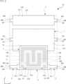
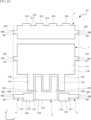
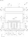
図1~図9に基づき、本開示の第1実施形態にかかる半導体装置A1について説明する。半導体装置A1は、複数のリード1~5、接続リード6、半導体素子7、および封止樹脂8を備えている。1 to 9, a semiconductor device A1 according to a first embodiment of the present disclosure will be described. The semiconductor device A1 includes a plurality of
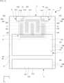
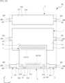
図1は、半導体装置A1を示す斜視図である。図2および図3は、半導体装置A1を示す平面図である。図2においては、理解の便宜上、封止樹脂8および接続リード6を透過して、封止樹脂8の外形を想像線(二点鎖線)で示している。図3においては、さらに半導体素子7を透過している。図4は、半導体装置A1を示す正面図である。図5は、半導体装置A1を示す底面図である。図6は、半導体装置A1を示す右側面図である。図7は、図1のVII-VII線に沿う断面図である。図8は、半導体素子7を示す平面図である。図9は、半導体素子7を示す模式的な断面図である。Figure 1 is a perspective view showing semiconductor device A1. Figures 2 and 3 are plan views showing semiconductor device A1. In Figure 2, for ease of understanding, the outer shape of the sealing
これらの図に示す半導体装置A1は、様々な機器の回路基板に表面実装される装置である。半導体装置A1の厚さ方向視の形状は矩形状である。説明の便宜上、半導体装置A1の厚さ方向をz方向とし、z方向に直交する半導体装置A1の一方の辺に沿う方向(図2における左右方向)をx方向、z方向およびx方向に直交する方向(図2における上下方向)をy方向とする。z方向が本開示の「厚さ方向」に相当する。半導体装置A1の大きさは特に限定されず、本実施形態においては、たとえばx方向寸法が1~10mm程度、y方向寸法が1~20mm程度、z方向寸法が0.3~3mm程度である。The semiconductor device A1 shown in these figures is a device that is surface-mounted on the circuit board of various devices. The shape of the semiconductor device A1 when viewed in the thickness direction is rectangular. For convenience of explanation, the thickness direction of the semiconductor device A1 is the z direction, the direction along one side of the semiconductor device A1 perpendicular to the z direction (the left-right direction in FIG. 2) is the x direction, and the direction perpendicular to the z direction and the x direction (the up-down direction in FIG. 2) is the y direction. The z direction corresponds to the "thickness direction" in this disclosure. The size of the semiconductor device A1 is not particularly limited, and in this embodiment, for example, the x direction dimension is about 1 to 10 mm, the y direction dimension is about 1 to 20 mm, and the z direction dimension is about 0.3 to 3 mm.
複数のリード1~5は、半導体素子7を支持するとともに、半導体素子7と導通している。リード1~5は、金属からなり、好ましくはCuおよびNiのいずれか、またはこれらの合金や42アロイなどからなる。本実施形態においては、リード1~5が、Cuからなる場合を例に説明する。リード1~5の厚さは、たとえば0.08~1mmであり、本実施形態においては0.5mm程度である。リード1~5は、たとえば、金属板にエッチング加工を施すことで形成されている。なお、リード1~5は、金属板に打ち抜き加工や折り曲げ加工等を施すことにより形成されてもよい。以降の説明においては、リード1~5を個別に説明する場合は、第1リード1、第2リード2、第3リード3、第4リード4、および第5リード5と記載する。なお、まとめて示す場合は、リード1~5のように記載する。The multiple leads 1 to 5 support the
図3に示すように、第1リード1は、半導体装置A1のy方向の略中央に配置され、x方向の全体に広がっている。第2リード2と第3リード3とは、y方向において、第1リード1を挟んで互いに反対側に、それぞれ第1リード1から離間して配置されている。第2リード2は、y方向の一方側(図3においては下側)の端部であり、かつ、x方向の略中央に配置されている。第3リード3は、y方向の他方側(図3においては上側)の端部に配置され、x方向の全体に広がっている。第4リード4および第5リード5は、y方向において、第1リード1に対して第2リード2と同じ側(図3においては下側)に、それぞれ第1リード1から離間して配置されている。つまり、z方向視において、第3リード3と、第2リード2、第4リード4、および第5リード5とは、第1リード1を挟んで互いに反対側に配置されている。また、第4リード4および第5リード5は、x方向において、第2リード2を挟んで互いに反対側に、それぞれ第2リード2から離間して配置されている。第4リード4は、y方向の一方側の端部であり、かつ、x方向の一方側(図3においては左側)の端部に配置されている。第5リード5は、y方向の一方側の端部であり、かつ、x方向の他方側(図3においては右側)の端部に配置されている。第1リード1は、z方向視寸法が、他のリード2~5に比べて大きい。z方向視寸法は、第3リード3、第2リード2の順に小さくなり、第4リード4および第5リード5が同程度であって最小である。As shown in FIG. 3, the
第1リード1は、端子部110、連結部120、および延出部130を備えている。The
端子部110は、z方向視において、x方向に長い矩形状である。端子部110は、端子部主面111および端子部裏面112を有する。端子部主面111および端子部裏面112は、z方向において互いに反対側を向いている。端子部主面111は、図4、図6および図7の上方を向く面である。端子部主面111は、半導体素子7の一部が接合される面である。端子部裏面112は、図4、図6および図7の下方を向く面である。端子部裏面112は、封止樹脂8から露出して、裏面端子になる。なお、端子部110は、端子部110の一部が端子部裏面112からz方向に凹んだ裏面側凹部を、たとえばハーフエッチング処理により形成されてもよい。When viewed in the z direction, the
連結部120は、端子部110に繋がっており、z方向視矩形状である。連結部120は、端子部110のx方向の一方端面に1個配置されている。また、連結部120は、端子部110のx方向の他方端面にも1個配置されている。つまり、連結部120は、合計2個配置されている。各連結部120は、連結部主面121、連結部裏面122、および連結部端面123を有する。連結部主面121および連結部裏面122は、z方向において互いに反対側を向いている。連結部主面121は、図4、図6および図7の上方を向く面である。連結部主面121と端子部主面111とは、面一になっている。連結部裏面122は、図4、図6および図7の下方を向く面である。連結部120の厚さ(z方向の寸法)は、端子部110の厚さの半分同程度である。連結部120は、たとえばハーフエッチング処理により形成される。連結部端面123は、連結部主面121および連結部裏面122を繋ぐ面であり、x方向外側を向いている。連結部端面123は、封止樹脂8から露出している(図1および図6参照)。The connecting
延出部130は、端子部110に繋がっており、z方向視においてy方向に長い矩形状である。延出部130は、端子部110のy方向の一方端面(図3における下方の端面)から、y方向に延びている。つまり、延出部130は、端子部110から第2リード2側に向かって延びている。本実施形態では、延出部130は、x方向に等間隔で並んで、3個配置されている。つまり、第1リード1は、z方向視において、全体として櫛歯状に形成されている。各延出部130は、延出部主面131および延出部裏面132を有する。延出部主面131および延出部裏面132は、z方向において互いに反対側を向いている。延出部主面131は、図4、図6および図7の上方を向く面である。延出部主面131は、半導体素子7の一部が接合される面である。延出部主面131と端子部主面111とは、面一になっている。したがって、端子部主面111、連結部主面121、および延出部主面131は、面一の一体となった面になっている(図3参照)。延出部裏面132は、図4、図6および図7の下方を向く面である。延出部130の厚さ(z方向の寸法)は、端子部110の厚さの半分同程度である。延出部130は、たとえばハーフエッチング処理により形成される。延出部130は、全体が封止樹脂8に覆われており、封止樹脂8から露出していない。延出部130が、本開示の「第1延出部」に相当する。The
第2リード2は、支持部210および延出部230を備えている。The
支持部210は、z方向視において、x方向に長い矩形状である。支持部210は、支持部主面211、支持部裏面212、および支持部端面213を有する。支持部主面211および支持部裏面212は、z方向において互いに反対側を向いている。支持部主面211は、図4、図6および図7の上方を向く面である。支持部主面211は、半導体素子7の一部が接合される面である。支持部裏面212は、図4、図6および図7の下方を向く面である。支持部210の厚さ(z方向の寸法)は、第1リード1の端子部110の厚さの半分同程度である。支持部210は、たとえばハーフエッチング処理により形成される。支持部主面211および支持部裏面212は、封止樹脂8から露出していない。支持部端面213は、支持部主面211および支持部裏面212を繋ぐ面であり、y方向外側(図3においては下側)を向いている。支持部端面213は、封止樹脂8から露出している(図1および図4参照)。The
延出部230は、支持部210に繋がっており、z方向視においてy方向に長い矩形状である。延出部230は、支持部210のy方向の他方端面(図3における上方の端面)から、y方向に延びている。つまり、延出部230は、支持部210から第1リード1側に向かって延びている。本実施形態では、延出部230は、x方向に並んで2個配置されている。つまり、第2リード2は、z方向視において、全体として櫛歯状に形成されている。また、各延出部230は、第1リード1の延出部130の間に配置されている。つまり、延出部130と延出部230とは、x方向において交互に配置されている。各延出部230は、延出部主面231および延出部裏面232を有する。延出部主面231および延出部裏面232は、z方向において互いに反対側を向いている。延出部主面231は、図4、図6および図7の上方を向く面である。延出部主面231は、半導体素子7の一部が接合される面である。延出部主面231と支持部主面211とは、面一になっている。延出部裏面232は、図4、図6および図7の下方を向く面である。延出部裏面232と支持部裏面212とは、面一になっている。つまり、延出部230の厚さ(z方向の寸法)は、支持部210の厚さと同程度である。延出部230は、たとえばハーフエッチング処理により形成される。延出部230は、全体が封止樹脂8に覆われており、封止樹脂8から露出していない。延出部230が、本開示の「第2延出部」に相当する。The
第3リード3は、端子部310および連結部320を備えている。The
端子部310は、z方向視において、x方向に長い矩形状である。端子部310は、端子部主面311、端子部裏面312、および端子部端面313を有する。端子部主面311および端子部裏面312は、z方向において互いに反対側を向いている。端子部主面311は、図4、図6および図7の上方を向く面である。端子部主面311は、半導体素子7の一部が接合される面である。端子部裏面312は、図4、図6および図7の下方を向く面である。端子部裏面312は、封止樹脂8から露出して、裏面端子になる。端子部310の厚さ(z方向の寸法)は、第1リード1の端子部110の厚さと同程度である。なお、端子部310は、端子部310の一部が端子部裏面312からz方向に凹んだ裏面側凹部を、たとえばハーフエッチング処理により形成されてもよい。端子部端面313は、端子部主面311および端子部裏面312を繋ぐ面であり、y方向外側(図3においては上側)、すなわち、第1リード1とは反対側を向いている。端子部端面313は、封止樹脂8から露出して端子になる。端子部端面313が、本開示の「第3端面」に相当する。The
連結部320は、端子部310に繋がっており、z方向視矩形状である。連結部320は、端子部310のx方向の一方端面に1個配置されている。また、連結部320は、端子部310のx方向の他方端面にも1個配置されている。つまり、連結部320は、合計2個配置されている。各連結部320は、連結部主面321、連結部裏面322、および連結部端面323を有する。連結部主面321および連結部裏面322は、z方向において互いに反対側を向いている。連結部主面321は、図4、図6および図7の上方を向く面である。連結部主面321と端子部主面311とは、面一になっている。連結部裏面322は、図4、図6および図7の下方を向く面である。連結部320の厚さ(z方向の寸法)は、端子部310の厚さの半分同程度である。連結部320は、たとえばハーフエッチング処理により形成される。連結部端面323は、連結部主面321および連結部裏面322を繋ぐ面であり、x方向外側を向いている。連結部端面323は、封止樹脂8から露出している(図1および図6参照)。The connecting
第4リード4は、端子部410および連結部420を備えている。The
端子部410は、z方向視において、x方向に長い矩形状である。端子部410は、端子部主面411、端子部裏面412および端子部端面413を有する。端子部主面411および端子部裏面412は、z方向において互いに反対側を向いている。端子部主面411は、図4、図6および図7の上方を向く面である。端子部主面411は、半導体素子7の一部が接合される面である。端子部裏面412は、図4、図6および図7の下方を向く面である。端子部裏面412は、封止樹脂8から露出して、裏面端子になる。端子部410の厚さ(z方向の寸法)は、第1リード1の端子部110の厚さと同程度である。なお、端子部410は、端子部410の一部が端子部裏面412からz方向に凹んだ裏面側凹部を、たとえばハーフエッチング処理により形成されてもよい。端子部端面413は、端子部主面411および端子部裏面412を繋ぐ面であり、y方向外側(図3においては下側)、すなわち、第1リード1とは反対側を向いている。端子部端面413は、封止樹脂8から露出して端子になる。端子部端面413が、本開示の「第4端面」に相当する。The
連結部420は、端子部410に繋がっており、z方向視においてx方向に長い矩形状である。連結部420は、端子部410のx方向の一方端面(図3における左側の端面)に1個配置されている。連結部420は、連結部主面421、連結部裏面422、および連結部端面423を有する。連結部主面421および連結部裏面422は、z方向において互いに反対側を向いている。連結部主面421は、図4、図6および図7の上方を向く面である。連結部主面421と端子部主面411とは、面一になっている。連結部裏面422は、図4、図6および図7の下方を向く面である。連結部420の厚さ(z方向の寸法)は、端子部410の厚さの半分同程度である。連結部420は、たとえばハーフエッチング処理により形成される。連結部端面423は、連結部主面421および連結部裏面422を繋ぐ面であり、x方向外側を向いている。連結部端面423は、封止樹脂8から露出している。The connecting
第5リード5は、端子部510および連結部520を備えている。The
端子部510は、z方向視において、x方向に長い矩形状である。端子部510は、端子部主面511、端子部裏面512および端子部端面513を有する。端子部主面511および端子部裏面512は、z方向において互いに反対側を向いている。端子部主面511は、図4、図6および図7の上方を向く面である。端子部主面511は、半導体素子7の一部が接合される面である。端子部裏面512は、図4、図6および図7の下方を向く面である。端子部裏面512は、封止樹脂8から露出して、裏面端子になる。端子部510の厚さ(z方向の寸法)は、第1リード1の端子部110の厚さと同程度である。なお、端子部510は、端子部510の一部が端子部裏面512からz方向に凹んだ裏面側凹部を、たとえばハーフエッチング処理により形成されてもよい。端子部端面513は、端子部主面511および端子部裏面512を繋ぐ面であり、y方向外側(図3においては下側)を向いている。端子部端面513は、封止樹脂8から露出して端子になる。The
連結部520は、端子部510に繋がっており、z方向視においてx方向に長い矩形状である。連結部520は、端子部510のx方向の他方端面(図3における右側の端面)に1個配置されている。連結部520は、連結部主面521、連結部裏面522、および連結部端面523を有する。連結部主面521および連結部裏面522は、z方向において互いに反対側を向いている。連結部主面521は、図4、図6および図7の上方を向く面である。連結部主面521と端子部主面511とは、面一になっている。連結部裏面522は、図4、図6および図7の下方を向く面である。連結部520の厚さ(z方向の寸法)は、端子部510の厚さの半分同程度である。連結部520は、たとえばハーフエッチング処理により形成される。連結部端面523は、連結部主面521および連結部裏面522を繋ぐ面であり、x方向外側を向いている。連結部端面523は、封止樹脂8から露出している(図1および図6参照)。The connecting
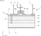
半導体素子7は、半導体装置A1の電気的機能を発揮する要素である。半導体素子7は、窒化物半導体を用いた半導体素子であり、本実施形態では、窒化ガリウム(GaN)を用いたHEMTである。半導体素子7は、素子本体70、ドレイン電極71、ソース電極72、ゲート電極73,74、および裏面電極75を備えている。半導体素子7は、ゲート電極73,74に印加される電圧信号に応じて、ドレイン電極71からソース電極72に流れる主電流を、流れる状態と流れない状態とで切り替える。つまり、半導体素子7は、主電流のスイッチングを行う。The
素子本体70は、素子主面7aおよび素子裏面7bを備えている。図4、図6および図7に示すように、素子主面7aおよび素子裏面7bは、z方向において互いに反対側を向いている。素子主面7aは、図4、図6および図7の上方を向く面である。素子裏面7bは、図4、図6および図7の下方を向く面である。また、素子本体70は、図9に示すように、基板701、バッファ層702、第1窒化物半導体層703、第2窒化物半導体層704、第3窒化物半導体層705、保護膜706、配線709、および導電部707を備えている。配線709は、配線709a,709b,709cを含んでいる。The
基板701は、たとえば低抵抗のSi基板である。基板701の厚さ(z方向の寸法)は、250~400μm程度である。バッファ層702は、基板701上に形成された窒化物半導体膜の多層バッファ層によって構成されている。本実施形態では、バッファ層702は、基板701に接するAlN膜からなる第1バッファ層と、当該第1バッファ層に積層されたAlGaN膜からなる第2バッファ層とによって構成されている。第2バッファ層は、AlN膜とGaN膜が交互に多重積層された超格子構造などでもよい。第1窒化物半導体層703は、バッファ層702上にエピタキシャル成長により積層されたGaN層からなり、電子走行層を構成している。第2窒化物半導体層704は、第1窒化物半導体層703上にエピタキシャル成長により積層されたAlGaN層からなり、電子供給層を構成している。バッファ層702、第1窒化物半導体層703および第2窒化物半導体層704を合わせた厚さ(z方向の寸法)は、2μm程度であり、基板701の厚さに比べて薄い。第1窒化物半導体層703の第2窒化物半導体層704との界面に近い位置に発生する二次元電子ガス(2DEG:2 Dimensional Electron Gas)が通電経路に用いられる。The
第3窒化物半導体層705は、第2窒化物半導体層704上にエピタキシャル成長により積層されたp型GaN層からなる。第3窒化物半導体層705上に、配線709aが形成されている。保護膜706は、たとえばSiN膜からなり、第2窒化物半導体層704、第3窒化物半導体層705、配線709aを覆う。配線709aの一部は、保護膜706から露出して、ゲート電極73,74に接続している。ゲート電極73,74は、半導体素子7のゲート電極として機能する。保護膜706上には、配線709b,709cが形成されている。配線709b,709cは、互いに離間して配置され、それぞれの一部が保護膜706を貫通して第2窒化物半導体層704に接している。配線709bは、第3窒化物半導体層705および配線709aを覆うように形成され、ソース電極72に接続している。ソース電極72は半導体素子7のソース電極として機能する。配線709cは、配線709bに隣接して形成され、ドレイン電極71に接続している。ドレイン電極71は、半導体素子7のドレイン電極として機能する。The third
図8に示すように、ドレイン電極71、ソース電極72、ゲート電極73、およびゲート電極74は、素子主面7aに配置されている。各電極71~74は、互いに離間しており、リード1~5の配置に応じて配置されている。ドレイン電極71は、素子主面7aのy方向の一方側(図8における下側)に配置され、x方向の全体に広がっている。ドレイン電極71は、帯状部711および3個の延出部712を有する。帯状部711は、z方向視においてx方向に長い矩形状であり、素子主面7aのy方向の一方端に配置されている。各延出部712は、帯状部711のx方向における両端および中心からy方向にそれぞれ延び、z方向視においてy方向に長い矩形状である。ソース電極72は、素子主面7aのy方向の他方側(図8における上側)で、x方向の中央に配置されている。ソース電極72は、帯状部721および2個の延出部722を有する。帯状部721は、z方向視においてx方向に長い矩形状であり、素子主面7aのy方向の他方端に配置されている。各延出部722は、帯状部721のx方向における両端からy方向にそれぞれ延び、z方向視においてy方向に長い矩形状である。各延出部722は、延出部712の間に配置されている。つまり、延出部712と延出部722とは、x方向において交互に配置されている。ゲート電極73は、素子主面7aのy方向の他方側で、x方向の一方側(図8における左側)に配置されている。ゲート電極73は、z方向視においてx方向に長い矩形状である。ゲート電極74は、素子主面7aのy方向の他方側で、x方向の他方側(図8における右側)に配置されている。ゲート電極74は、z方向視においてx方向に長い矩形状である。なお、各電極71~74の配置および形状は限定されず、リード1~5の配置および形状と連動して設計される。As shown in FIG. 8, the
裏面電極75は、基板701の裏面(バッファ層702が形成される面とは反対側を向く面)に形成されており、素子裏面7bに配置されている。The
導電部707は、たとえばビアホールであり、第2窒化物半導体層704、第1窒化物半導体層703、およびバッファ層702を貫通して基板701まで達している。導電部707は、保護膜706を貫通した配線709bに接して導通しており、基板701を介して裏面電極75にも導通している。したがって、ソース電極72と裏面電極75とは導通して同電位になる。なお、導電部707は、基板701も貫通して裏面電極75まで達してもよい。また、後述するように、ソース電極72と裏面電極75とは、第2リード2および接続リード6を介して導通し、同電位になるので、半導体素子7は、導電部707を備えなくてもよい。The
半導体素子7は、第1リード1、第2リード2、第4リード4、および第5リード5にフリップチップボンディングされている。つまり、半導体素子7は、素子主面7aをリード1,2,4,5の各主面に向けて、図示しない導電性接合材を介して、リード1,2,4,5に接合されている。半導体素子7は、z方向視において、第1リード1の延出部130および第2リード2の延出部230に重なり、第1リード1の端子部110、第2リード2の支持部210、第4リード4の端子部410、および第5リード5の端子部510のそれぞれ一部ずつに重なるように配置されている。つまり、半導体素子7は、延出部130および延出部230と、端子部110、支持部210、端子部410、および端子部510のそれぞれ一部ずつとによって支持されている。The
ドレイン電極71は、第1リード1に接合されている。より具体的には、ドレイン電極71の帯状部711は第1リード1の端子部主面111に接合され、ドレイン電極71の各延出部712は、それぞれ、第1リード1の延出部主面131に接合されている。これにより、第1リード1は、半導体素子7のドレイン電極71に電気的に接続されて、半導体素子7のドレイン端子として機能する。ソース電極72は、第2リード2に接合されている。より具体的には、ソース電極72の帯状部721は第2リード2の支持部主面211に接合され、ソース電極72の各延出部722は、それぞれ、第2リード2の延出部主面231に接合されている。また、後述するように、第2リード2は、接続リード6によって第3リード3に電気的に接続されている。これにより、第3リード3は、半導体素子7のソース電極72に電気的に接続されて、半導体素子7のソース端子として機能する。ゲート電極73は、第4リード4の端子部主面411に接合されている。これにより、第4リード4は、半導体素子7のゲート電極73に電気的に接続され、半導体素子7のゲート端子として機能する。また、ゲート電極74は、第5リード5の端子部主面511に接合されている。これにより、第5リード5は、半導体素子7のゲート電極74に電気的に接続され、半導体素子7のゲート端子として機能する。The
接続リード6は、第2リード2と第3リード3とを電気的に接続し、主電流の電流経路となる部材である。接続リード6は、金属板からなり、好ましくはCuおよびNiのいずれか、またはこれらの合金や42アロイなどからなる。本実施形態においては、接続リード6が、Cuからなる場合を例に説明する。接続リード6の厚さは、たとえば0.08~1mmであり、本実施形態においては0.5mm程度である。接続リード6は、たとえば、金属板に打ち抜き加工および折り曲げ加工等を施すことにより形成されている。接続リード6は、第1板部61、第2板部62、および第3板部63を有する。The
図1に示すように、第1板部61は、略矩形板状であり、z方向に直交するように、半導体素子7の素子裏面7b側に配置されている。第1板部61は、z方向視において、一部が半導体素子7に重なっている。また、第1板部61は、z方向視において、第1リード1、第2リード2、および第3リード3に重なっている。半導体素子7は、z方向視において、第1板部61と、第1リード1および第2リード2とによって挟まれている。第1板部61は、第1板部主面61aおよび第1板部裏面61bを有する。第1板部主面61aおよび第1板部裏面61bは、z方向において互いに反対側を向いている。第1板部主面61aは、図4、図6および図7の上方を向く面である。第1板部主面61aは、封止樹脂8から露出している。第1板部裏面61bは、図4、図6および図7の下方を向く面である。第1板部裏面61bは、半導体素子7の素子裏面7bに接触しており、図示しない導電性接合材を介して素子裏面7bに接合されている。素子裏面7bに形成されている裏面電極75は、導電性接合材を介して第1板部裏面61bに接合されている。第1板部61は、y方向の各端部で、第2板部62および第3板部63に繋がっている。第1板部61の第2板部62と繋がる端部のx方向の寸法は第2板部62のx方向の寸法に一致し、第1板部61の第3板部63と繋がる端部のx方向の寸法は第3板部63のx方向の寸法に一致している。1, the
第2板部62は、略矩形板状であり、z方向およびx方向に平行になるように、半導体素子7のy方向の一方側(図6および図7においては左側)に配置されている。第2板部62のz方向の一方端(図6および図7における上方端)は、第1板部61に接続している。第1板部61と第2板部62とは直交している。第2板部62のz方向の他方端(図6および図7における下方端)は、図示しない導電性接合材を介して、第2リード2の支持部主面211に接続している。第2板部62と第2リード2とは直交している。第2板部62は、封止樹脂8に覆われており、樹脂側面83から露出していない。The
第3板部63は、略矩形板状であり、z方向およびx方向に平行になるように、半導体素子7のy方向の他方側(図6および図7においては右側)に配置されている。第3板部63のz方向の一方端(図6および図7における上方端)は、第1板部61に接続している。第1板部61と第3板部63とは直交している。第3板部63のz方向の他方端(図6および図7における下方端)は、図示しない導電性接合材を介して、第3リード3の端子部主面311に接続している。第3板部63と第3リード3とは直交している。第3板部63は、封止樹脂8に覆われており、樹脂側面83から露出していない。The
半導体素子7が導通状態のとき、半導体装置A1の内部には、図7の破線矢印に示すように電流が流れる。すなわち、電流は、ドレイン端子である第1リード1から入力されて、第1リード1から半導体素子7のドレイン電極71に流れる。そして、電流は、半導体素子7の内部において、ドレイン電極71からソース電極72に流れる。半導体素子7の内部においては、電流はさまざまな方向に流れるが、各電流が打ち消し合って、総合的にみると、図7の半導体素子7の内部に示す破線矢印の方向に流れる。ソース電極72から出力された電流は、第2リード2および接続リード6を流れ、ソース端子である第3リード3から出力される。When the
封止樹脂8は、各リード1~5および接続リード6の一部ずつと、半導体素子7とを覆っている。封止樹脂8は、たとえば黒色のエポキシ樹脂からなる。The sealing
封止樹脂8は、樹脂主面81、樹脂裏面82および樹脂側面83を有する。樹脂主面81と樹脂裏面82とは、z方向において互いに反対側を向いている。樹脂主面81は、図4、図6および図7の上方を向く面であり、樹脂裏面82は、図4、図6および図7の下方を向く面である。樹脂側面83は、樹脂主面81および樹脂裏面82を繋ぐ面であり、x方向またはy方向を向いている。The sealing
本実施形態においては、第1リード1の連結部端面123と、第2リード2の支持部端面213と、第3リード3の端子部端面313および連結部端面323と、第4リード4の端子部端面413および連結部端面423と、第5リード5の端子部端面513および連結部端面523とが、封止樹脂8の樹脂側面83と互いに面一である。また、第1リード1の端子部裏面112と、第3リード3の端子部裏面312と、第4リード4の端子部裏面412と、第5リード5の端子部裏面512とが、封止樹脂8の樹脂裏面82と互いに面一である。また、接続リード6の第1板部主面61aが、封止樹脂8の樹脂主面81と互いに面一である。In this embodiment, the connecting
次に、半導体装置A1の製造方法の一例について、以下に説明する。Next, an example of a manufacturing method for semiconductor device A1 will be described below.
まず、リードフレームを用意する。リードフレームは、各リード1~5となる板状の材料である。リードフレームのうち、第1リード1の連結部120および延出部130と、第2リード2の支持部210および延出部230と、第3リード3の連結部320と、第4リード4の連結部420と、第5リード5の連結部520となる領域は、たとえばハーフエッチング処理によって、他の領域より、厚さ(z方向の寸法)を薄く形成されている。本実施形態においては、リードフレームの母材は、Cuからなる。First, a lead frame is prepared. The lead frame is a plate-shaped material that will become each of the
次いで、リードフレームの所定の位置に、半導体素子7を導電性接合材によって、フリップチップボンディングする。次いで、別途形成された接続リード6を、半導体素子7に跨るように配置し、導電性接合材によって、リードフレームのうち第2リード2および第3リード3になる領域と、半導体素子7の素子裏面7bとに接合する。Next, the
次いで、樹脂材料を硬化させることにより、半導体素子7、リードフレームの一部、および接続リード6の一部を覆う封止樹脂を形成する。次いで、リードフレームおよび封止樹脂を、切断線に沿って切断する。これにより、半導体装置A1となる個片が形成される。以上の工程を経ることにより、上述した半導体装置A1が得られる。The resin material is then cured to form an encapsulating resin that covers the
次に、半導体装置A1の作用効果について説明する。Next, the effects of the semiconductor device A1 will be explained.
本実施形態によると、半導体素子7が導通状態のとき、スイッチングの対象である主電流は、ドレイン端子である第1リード1から入力されて、第1リード1から半導体素子7のドレイン電極71に流れ、半導体素子7の内部において、ドレイン電極71からソース電極72に流れる。そして、ソース電極72から出力された主電流は、第2リード2および接続リード6を流れ、ソース端子である第3リード3から出力される。半導体素子7はフリップチップボンディングされ、ドレイン電極71が第1リード1に接合され、ソース電極72が第2リード2に接合されている。したがって、ボンディングワイヤで接続された場合と比較して、電流経路が短縮されるので、インダクタンスは低減される。また、接続リード6は、第1板部61が半導体素子7の素子裏面7b側でz方向視において一部が半導体素子7に重なるように配置されており、第2リード2と第3リード3とに接続している。したがって、接続リード6には、第1リード1から第2リード2までの電流経路とは反対方向に主電流が流れる。第1リード1から第2リード2までの電流経路を流れる主電流により発生する磁場と、接続リード6を流れる主電流により発生する磁場とが打ち消し合うので、発生するインダクタンスは低減される。According to this embodiment, when the
また、本実施形態によると、接続リード6の第1板部61は、第1板部裏面61bが半導体素子7の素子裏面7bに接合されており、第1板部主面61aが封止樹脂8から露出している。つまり、第1板部61は、半導体素子7から発生する熱を放熱する放熱板として機能する。これにより、半導体素子7の温度上昇が抑制される。また、接続リード6は、半導体素子7から発生するノイズの遮蔽板としても機能する。これにより、半導体装置A1から放射されるノイズは低減される。In addition, according to this embodiment, the
また、本実施形態によると、第1リード1が延出部130を備え、第2リード2が延出部230を備えている。これにより、半導体素子7は適切に支持され、ドレイン電極71と第1リード1、および、ソース電極72と第2リード2の導通がより確実に行われる。また、延出部130および延出部230は、樹脂裏面82から露出していない。これにより、半導体装置A1を実装するときに、はんだペーストによって延出部130と延出部230とが繋がることがなく、第1リード1と第2リード2との短絡が防止される。In addition, according to this embodiment, the
なお、本実施形態では、半導体素子7がHEMTである場合について説明したが、これに限られない。半導体素子7は、ドレイン電極71とソース電極72とが同じ面に配置され、半導体素子7の内部をz方向に直交する方向に主電流が流れるものであればよい。In this embodiment, the
また、本実施形態では、第1板部裏面61bが半導体素子7の素子裏面7bに接合されている場合について説明したが、これに限られない。第1板部裏面61bは、素子裏面7bに接合されていなくてもよいし、素子裏面7bとの間に封止樹脂8が充填されていてもよい。In addition, in this embodiment, the case where the first plate portion back
図10に基づき、本開示の第2実施形態にかかる半導体装置A2について説明する。図10において、先述した半導体装置A1と同一または類似の要素には同一の符号を付して、重複する説明を省略する。A semiconductor device A2 according to a second embodiment of the present disclosure will be described with reference to Fig. 10. In Fig. 10, elements that are the same as or similar to the semiconductor device A1 described above are given the same reference numerals, and duplicate descriptions will be omitted.
図10は、半導体装置A2を示す断面図であり、第1実施形態における図7に対応する図である。Figure 10 is a cross-sectional view showing semiconductor device A2, which corresponds to Figure 7 in the first embodiment.
本実施形態にかかる半導体装置A2は、接続リード6の形状が半導体装置A1と異なる。第2実施形態にかかる接続リード6は、第2板部62および第3板部63が、z方向に対して傾斜している。The semiconductor device A2 in this embodiment differs from the semiconductor device A1 in the shape of the
本実施形態においても、半導体素子7がフリップチップボンディングされているので、インダクタンスは低減される。また、接続リード6には、第1リード1から第2リード2までの電流経路とは反対方向に主電流が流れるので、発生する磁場が打ち消し合って、発生するインダクタンスは低減される。したがって、本実施形態においても、第1実施形態と同様の効果を奏することができる。In this embodiment, the
図11に基づき、本開示の第3実施形態にかかる半導体装置A3について説明する。図11において、先述した半導体装置A1と同一または類似の要素には同一の符号を付して、重複する説明を省略する。A semiconductor device A3 according to a third embodiment of the present disclosure will be described with reference to Fig. 11. In Fig. 11, elements that are the same as or similar to the semiconductor device A1 described above are given the same reference numerals, and duplicate descriptions will be omitted.
図11は、半導体装置A3を示す断面図であり、第1実施形態における図7に対応する図である。Figure 11 is a cross-sectional view showing semiconductor device A3, which corresponds to Figure 7 in the first embodiment.
本実施形態にかかる半導体装置A3は、第1板部主面61aが封止樹脂8の樹脂主面81から露出しない点で、半導体装置A1と異なる。第3実施形態にかかる接続リード6は、全体が封止樹脂8によって覆われている。The semiconductor device A3 according to this embodiment differs from the semiconductor device A1 in that the first plate portion
本実施形態においても、半導体素子7がフリップチップボンディングされているので、インダクタンスは低減される。また、接続リード6には、第1リード1から第2リード2までの電流経路とは反対方向に主電流が流れるので、発生する磁場が打ち消し合って、発生するインダクタンスは低減される。また、接続リード6は半導体素子7から発生するノイズの遮蔽板として機能するので、半導体装置A1から放射されるノイズは低減される。In this embodiment, the
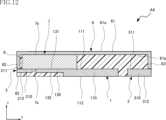
図12に基づき、本開示の第4実施形態にかかる半導体装置A4について説明する。図12において、先述した半導体装置A1と同一または類似の要素には同一の符号を付して、重複する説明を省略する。A semiconductor device A4 according to the fourth embodiment of the present disclosure will be described with reference to Fig. 12. In Fig. 12, elements that are the same as or similar to the semiconductor device A1 described above are given the same reference numerals, and duplicate descriptions will be omitted.
図12は、半導体装置A4を示す断面図であり、第1実施形態における図7に対応する図である。Figure 12 is a cross-sectional view showing semiconductor device A4, which corresponds to Figure 7 in the first embodiment.
本実施形態にかかる半導体装置A4は、接続リード6の第2板部62および第3板部63が樹脂側面83から露出している点で、半導体装置A1と異なる。The semiconductor device A4 in this embodiment differs from the semiconductor device A1 in that the
本実施形態においても、第1実施形態と同様の効果を奏することができる。また、本実施形態によると、接続リード6の第2板部62および第3板部63も樹脂側面83から露出しているので、放熱性がさらに向上する。In this embodiment, the same effects as in the first embodiment can be achieved. In addition, in this embodiment, the
図13および図14に基づき、本開示の第5実施形態にかかる半導体装置A5について説明する。図13および図14において、先述した半導体装置A1と同一または類似の要素には同一の符号を付して、重複する説明を省略する。A semiconductor device A5 according to a fifth embodiment of the present disclosure will be described with reference to Figures 13 and 14. In Figures 13 and 14, elements that are the same as or similar to the semiconductor device A1 described above are given the same reference numerals, and duplicate descriptions will be omitted.
図13は、半導体装置A5を示す断面図であり、第1実施形態における図7に対応する図である。図14は、半導体装置A5を示す正面図であり、第1実施形態における図4に対応する図である。Figure 13 is a cross-sectional view of semiconductor device A5, which corresponds to Figure 7 in the first embodiment. Figure 14 is a front view of semiconductor device A5, which corresponds to Figure 4 in the first embodiment.
本実施形態にかかる半導体装置A5は、接続リード6と第2リード2および第3リード3との接続方法が異なる点で、半導体装置A1と異なる。The semiconductor device A5 in this embodiment differs from the semiconductor device A1 in that the method of connecting the
第5実施形態にかかる接続リード6は、第2板部62および第3板部63を備えておらず、第1板部61だけである。接続リード6と第2リード2および第3リード3とは、それぞれ2個の柱状部65によって接続されている。柱状部65は、接続リード6と第2リード2および第3リード3とを接続する導電体である。本実施形態では、柱状部65は、z方向に直交する断面が矩形の角柱形状である。なお、柱状部65の形状は限定されず、たとえば円柱形状などであってもよい。柱状部65のz方向の一方端(図13および図14における上方端)は、図示しない導電性接合材を介して、第1板部61に接続している。柱状部65のz方向の他方端(図13および図14における下方端)は、図示しない導電性接合材を介して、第2リード2の支持部主面211または第3リード3の端子部主面311に接続している。本実施形態では、柱状部65は、たとえばCuからなる。なお、柱状部65の材料や形成方法、形状、個数は限定されない。The
本実施形態においても、第1実施形態と同様の効果を奏することができる。なお、本実施形態においては、接続リード6と第2リード2および第3リード3とが柱状部65によって接続される場合ついて説明したが、これに限られない。接続リード6と第2リード2および第3リード3とは、たとえばボンディングワイヤなどのその他の導電部材によって接続されてもよい。In this embodiment, the same effects as in the first embodiment can be achieved. In this embodiment, the
図15に基づき、本開示の第6実施形態にかかる半導体装置A6について説明する。図15において、先述した半導体装置A1と同一または類似の要素には同一の符号を付して、重複する説明を省略する。A semiconductor device A6 according to a sixth embodiment of the present disclosure will be described with reference to Fig. 15. In Fig. 15, elements that are the same as or similar to the semiconductor device A1 described above are given the same reference numerals, and duplicate descriptions will be omitted.
図15は、半導体装置A6を示す断面図であり、第1実施形態における図7に対応する図である。Figure 15 is a cross-sectional view showing semiconductor device A6, which corresponds to Figure 7 in the first embodiment.
本実施形態にかかる半導体装置A6は、ソース端子がドレイン端子(第1リード1)とは反対側を向く面に配置されている点で、半導体装置A1と異なる。The semiconductor device A6 in this embodiment differs from the semiconductor device A1 in that the source terminal is arranged on the surface facing opposite the drain terminal (first lead 1).
第6実施形態にかかる半導体装置A6は、第2リード2を備えていない。また、第6実施形態にかかる接続リード6は、第3板部63を備えていない。接続リード6の第1板部61は、第1板部主面61aからz方向に突出した突出面61cを備えている。第1板部主面61aは、封止樹脂8によって覆われている。一方、突出面61cは封止樹脂8から露出し、樹脂主面81と互いに面一になっている。封止樹脂8から露出した突出面61cが、ソース端子になる。The semiconductor device A6 according to the sixth embodiment does not include a
本実施形態においても、第1実施形態と同様の効果を奏することができる。さらに、本実施形態によると、第2リード2が配置されていないので、y方向の寸法を小さくすることができる。In this embodiment, the same effects as in the first embodiment can be achieved. Furthermore, in this embodiment, since the
図16および図17に基づき、本開示の第7実施形態にかかる半導体装置A7について説明する。図16および図17において、先述した半導体装置A1と同一または類似の要素には同一の符号を付して、重複する説明を省略する。16 and 17, a semiconductor device A7 according to a seventh embodiment of the present disclosure will be described. In Fig. 16 and Fig. 17, elements that are the same as or similar to the semiconductor device A1 described above are given the same reference numerals, and duplicated descriptions will be omitted.
図16は、半導体装置A7を示す平面図であり、第1実施形態における図3に対応する図である。図16においては、理解の便宜上、封止樹脂8、接続リード6、および半導体素子7を透過して、封止樹脂8の外形を想像線(二点鎖線)で示している。図17は、半導体装置A7を示す右側面図であり、第1実施形態における図6に対応する図である。Figure 16 is a plan view showing semiconductor device A7, and corresponds to Figure 3 in the first embodiment. In Figure 16, for ease of understanding, the outline of the sealing
本実施形態にかかる半導体装置A7は、ゲート端子(第4リード4および第5リード5)とソース端子(第3リード3)の形状が、半導体装置A1と異なる。The semiconductor device A7 in this embodiment differs from the semiconductor device A1 in the shapes of the gate terminal (
第7実施形態にかかる第3リード3は、端子部端面313からy方向に突出する突出部314を備えている。突出部314は、z方向視においてx方向に長い矩形状である。突出部314は、端子部310のy方向外側を向く端面に、x方向に等間隔で並んで4個配置されている。なお、突出部314の個数は限定されない。The
また、第7実施形態においては、第4リード4の端子部端面413および第5リード5の端子部端面513が、樹脂側面83と面一ではなく、樹脂側面83から突出している。In addition, in the seventh embodiment, the
本実施形態においても、第1実施形態と同様の効果を奏することができる。なお、第4リード4の端子部端面413および第5リード5の端子部端面513は、樹脂側面83から凹んでいてもよい。また、これらの各端面は、平坦であってもよいし、湾曲していてもよいし、凹凸が形成されていてもよい。また、これらの各端面の形状も限定されない。また、第3リード3の端子部端面313が樹脂側面83に覆われ、突出部314が樹脂側面83から露出してもよい。また、第3リード3が突出部314を備えず、端子部端面313が樹脂側面83に覆われてもよい。In this embodiment, the same effect as in the first embodiment can be achieved. The
図18に基づき、本開示の第8実施形態にかかる半導体装置A8について説明する。図18において、先述した半導体装置A1と同一または類似の要素には同一の符号を付して、重複する説明を省略する。A semiconductor device A8 according to an eighth embodiment of the present disclosure will be described with reference to Fig. 18. In Fig. 18, elements that are the same as or similar to the semiconductor device A1 described above are given the same reference numerals, and duplicate descriptions will be omitted.
図18は、半導体装置A8を示す平面図であり、第1実施形態における図2に対応する図である。図18においては、理解の便宜上、封止樹脂8および接続リード6を透過して、封止樹脂8の外形を想像線(二点鎖線)で示している。18 is a plan view showing a semiconductor device A8, and corresponds to FIG. 2 in the first embodiment. In FIG. 18, for ease of understanding, the outline of the sealing
本実施形態にかかる半導体装置A8は、半導体素子7のドレイン電極71およびソース電極72の形状と、第1リード1および第2リード2の形状とが、半導体装置A1と異なる。The semiconductor device A8 in this embodiment differs from the semiconductor device A1 in the shapes of the
第8実施形態においては、第1リード1が延出部130を2個備え、第2リード2が延出部230を1個備えている。また、ドレイン電極71は延出部712を2個備え、ソース電極72は延出部722を1個備えている。In the eighth embodiment, the
本実施形態においても、第1実施形態と同様の効果を奏することができる。なお、第1リード1の延出部130の数、および、第2リード2の延出部230の数は限定されない。たとえば、延出部130が1個で、延出部230が2個であってもよい。ドレイン電極71の形状(延出部712の数も含む)およびソース電極72の形状(延出部722の数も含む)は、それぞれ、第1リード1の延出部130および第2リード2の延出部230の数および配置に応じて設計される。In this embodiment, the same effects as in the first embodiment can be achieved. The number of
図19に基づき、本開示の第9実施形態にかかる半導体装置A9について説明する。図19において、先述した半導体装置A1と同一または類似の要素には同一の符号を付して、重複する説明を省略する。A semiconductor device A9 according to the ninth embodiment of the present disclosure will be described with reference to Fig. 19. In Fig. 19, elements that are the same as or similar to the semiconductor device A1 described above are given the same reference numerals, and duplicate descriptions will be omitted.
図19は、半導体装置A9を示す平面図であり、第1実施形態における図2に対応する図である。図19においては、理解の便宜上、封止樹脂8および接続リード6を透過して、封止樹脂8の外形を想像線(二点鎖線)で示している。19 is a plan view showing the semiconductor device A9, and corresponds to FIG. 2 in the first embodiment. In FIG. 19, for ease of understanding, the outline of the sealing
本実施形態にかかる半導体装置A9は、半導体素子7のドレイン電極71およびソース電極72の形状と、第1リード1および第2リード2の形状とが、半導体装置A1と異なる。The semiconductor device A9 in this embodiment differs from the semiconductor device A1 in the shapes of the
第9実施形態においては、第1リード1が延出部130を備えておらず、第2リード2が延出部230を備えていない。また、ドレイン電極71は延出部712を備えておらず、ソース電極72は延出部722を備えていない。つまり、半導体素子7は、第1リード1の端子部110の一部、第2リード2の支持部210の一部、第4リード4の端子部410の一部、および第5リード5の端子部510の一部だけで支持されている。また、ドレイン電極71は、帯状部711だけで第1リード1の端子部主面111に接合され、ソース電極72は、帯状部721だけで第2リード2の支持部主面211に接合されている。In the ninth embodiment, the
本実施形態においても、半導体素子7がフリップチップボンディングされているので、インダクタンスは低減される。また、接続リード6には、第1リード1から第2リード2までの電流経路とは反対方向に主電流が流れるので、発生する磁場が打ち消し合って、発生するインダクタンスは低減される。また、接続リード6は半導体素子7から発生する熱を放熱する放熱板として機能するので、半導体素子7の温度上昇が抑制される。また、接続リード6は半導体素子7から発生するノイズの遮蔽板として機能するので、半導体装置A1から放射されるノイズは低減される。In this embodiment, the
図20に基づき、本開示の第10実施形態にかかる半導体装置A10について説明する 。図20において、先述した半導体装置A1と同一または類似の要素には同一の符号を付して、重複する説明を省略する。A semiconductor device A10 according to a tenth embodiment of the present disclosure will be described with reference to Fig. 20. In Fig. 20, elements that are the same as or similar to the semiconductor device A1 described above are given the same reference numerals, and duplicate descriptions will be omitted.
図20は、半導体装置A10を示す平面図であり、第1実施形態における図2に対応する図である。図20においては、理解の便宜上、封止樹脂8および接続リード6を透過して、封止樹脂8の外形を想像線(二点鎖線)で示している。20 is a plan view showing the semiconductor device A10, and corresponds to FIG. 2 in the first embodiment. In FIG. 20, for ease of understanding, the outline of the sealing
本実施形態にかかる半導体装置A10は、半導体素子7のドレイン電極71およびソース電極72の形状が、半導体装置A1と異なる。The semiconductor device A10 in this embodiment differs from the semiconductor device A1 in the shape of the
第10実施形態においては、ドレイン電極71は帯状部711を備えておらず、ソース電極72は帯状部721を備えていない。つまり、ドレイン電極71は、延出部712だけで第1リード1の延出部主面131および端子部主面111に接合され、ソース電極72は、延出部722だけで第2リード2の延出部主面231および支持部主面211に接合されている。In the tenth embodiment, the
本実施形態においても、第1実施形態と同様の効果を奏することができる。This embodiment can achieve the same effects as the first embodiment.
図21に基づき、本開示の第11実施形態にかかる半導体装置A11について説明する。図21において、先述した半導体装置A1と同一または類似の要素には同一の符号を付して、重複する説明を省略する。A semiconductor device A11 according to an eleventh embodiment of the present disclosure will be described with reference to Fig. 21. In Fig. 21, elements that are the same as or similar to the semiconductor device A1 described above are given the same reference numerals, and duplicate descriptions will be omitted.
図21は、半導体装置A11を示す底面図であり、第1実施形態における図5に対応する図である。Figure 21 is a bottom view showing semiconductor device A11, which corresponds to Figure 5 in the first embodiment.
本実施形態にかかる半導体装置A11は、第2リード2の支持部裏面212が封止樹脂8の樹脂裏面82から露出し、支持部裏面212と樹脂裏面82とが互いに面一である点で、半導体装置A1と異なる。なお、半導体装置A11が回路基板に表面実装される際に、第2リード2は、ソース端子として回路基板の配線に接合されない。The semiconductor device A11 according to this embodiment differs from the semiconductor device A1 in that the support portion back
本実施形態においても、第1実施形態と同様の効果を奏することができる。This embodiment can achieve the same effects as the first embodiment.
図22に基づき、本開示の第12実施形態にかかる半導体装置A12について説明する。図22において、先述した半導体装置A1と同一または類似の要素には同一の符号を付して、重複する説明を省略する。A semiconductor device A12 according to a twelfth embodiment of the present disclosure will be described with reference to Fig. 22. In Fig. 22, elements that are the same as or similar to the semiconductor device A1 described above are given the same reference numerals, and duplicate descriptions will be omitted.
図22は、半導体装置A12を示す底面図であり、第1実施形態における図5に対応する図である。Figure 22 is a bottom view showing semiconductor device A12, which corresponds to Figure 5 in the first embodiment.
本実施形態にかかる半導体装置A12は、第1リード1の延出部裏面132が封止樹脂8の樹脂裏面82から露出し、延出部裏面132と樹脂裏面82とが互いに面一である点で、半導体装置A1と異なる。なお、第2リード2の延出部裏面232は樹脂裏面82から露出しないので、半導体装置A12が回路基板に表面実装される際に、はんだペーストによって延出部130と延出部230とが繋がることがなく、第1リード1と第2リード2との短絡が防止される。The semiconductor device A12 according to this embodiment differs from the semiconductor device A1 in that the extension portion back
本実施形態においても、第1実施形態と同様の効果を奏することができる。また、本実施形態によると、延出部裏面132が樹脂裏面82から露出しているので、半導体装置A12が回路基板に表面実装された場合に、延出部裏面132を介して放熱することができる。したがって、放熱性がさらに向上する。なお、本実施形態では、第1リード1の延出部裏面132が樹脂裏面82から露出し、第2リード2の延出部裏面232が樹脂裏面82から露出しない場合について説明したが、第2リード2の延出部裏面232が樹脂裏面82から露出し、第1リード1の延出部裏面132が樹脂裏面82から露出しない場合も同様である。In this embodiment, the same effect as in the first embodiment can be achieved. In addition, according to this embodiment, since the extension portion back
本開示にかかる半導体装置は、先述した実施形態に限定されるものではない。本開示にかかる半導体装置の各部の具体的な構成は、種々に設計変更自在である。The semiconductor device according to the present disclosure is not limited to the above-described embodiment. The specific configuration of each part of the semiconductor device according to the present disclosure can be freely designed in various ways.
〔付記1〕
窒化物半導体からなる電子走行層と、厚さ方向において互いに反対側を向く素子主面および素子裏面と、前記素子主面に配置されたゲート電極、ソース電極、およびドレイン電極と、を有する半導体素子と、
前記ドレイン電極が接合されている第1リードと、
前記ソース電極が接合されている第2リードと、
前記第2リードに接続し、かつ、前記素子裏面側に、前記厚さ方向視において前記半導体素子に重なるように配置されている接続リードと、
を備え、
前記接続リードにはスイッチングの対象である主電流が流れる、
半導体装置。
〔付記2〕
前記接続リードは、前記素子裏面に接触している、付記1に記載の半導体装置。
〔付記3〕
前記半導体素子は、前記素子裏面に配置され、かつ、前記ソース電極と電気的に接続された裏面電極をさらに備え、
前記接続リードには、前記裏面電極が接合されている、付記2に記載の半導体装置。
〔付記4〕
前記半導体素子を覆う封止樹脂をさらに備え、
前記接続リードの一部は、前記封止樹脂から露出している、付記1ないし3のいずれかに記載の半導体装置。
〔付記5〕
前記封止樹脂は、前記厚さ方向において互いに反対側を向く樹脂主面および樹脂裏面と、前記樹脂主面および前記樹脂裏面に繋がる樹脂側面とを有する、付記4に記載の半導体装置。
〔付記6〕
前記第2リードは、前記樹脂主面および前記樹脂裏面から露出していない、付記5に記載の半導体装置。
〔付記7〕
前記接続リードは、金属板である、付記5または6に記載の半導体装置。
〔付記8〕
前記接続リードは、前記厚さ方向視において前記半導体素子に重なる第1板状部と、
前記第2リードと前記第1板状部とに接続する第2板状部と、
を備えている、付記7に記載の半導体装置。
〔付記9〕
前記第1リードに対して、前記第2リードとは反対側に配置されている第3リードをさらに備え、
前記接続リードは、前記第3リードと前記第1板状部とに接続する第3板状部をさらに備えている、付記8に記載の半導体装置。
〔付記10〕
前記第2板状部および前記第3板状部は、前記厚さ方向に平行である、付記9に記載の半導体装置。
〔付記11〕
前記第1リードおよび前記第3リードの一部は、前記樹脂裏面から露出している、付記9または10に記載の半導体装置。
〔付記12〕
前記第3リードは、前記第1リードとは反対側を向き、かつ、前記樹脂側面から露出する第3端面を備え、
前記第3端面と前記樹脂側面とは、互いに面一である、付記9ないし11のいずれかに記載の半導体装置。
〔付記13〕
前記第1リードに対して、前記第2リードと同じ側に配置され、かつ、前記ゲート電極が接合されている第4リードをさらに備えている、付記5ないし12のいずれかに記載の半導体装置。
〔付記14〕
前記第4リードは、前記第1リードとは反対側を向き、かつ、前記樹脂側面から露出する第4端面を備え、
前記第4端面と前記樹脂側面とは、互いに面一である、付記13に記載の半導体装置。
〔付記15〕
前記第1リードは、前記厚さ方向視において前記第2リード側に向かって延びる複数の第1延出部を備え、
前記第2リードは、前記厚さ方向視において前記第1リード側に向かって延び、かつ、前記複数の第1延出部の間に配置される第2延出部を備え、
前記半導体素子は、前記第1延出部および前記第2延出部によって支持されている、付記4ないし14のいずれかに記載の半導体装置。
〔付記16〕
前記第2リードは、前記厚さ方向視において前記第1リード側に向かって延びる複数の第2延出部を備え、
前記第1リードは、前記厚さ方向視において前記第2リード側に向かって延び、かつ、前記複数の第2延出部の間に配置される第1延出部を備え、
前記半導体素子は、前記第1延出部および前記第2延出部によって支持されている、付記4ないし14のいずれかに記載の半導体装置。
〔付記17〕
前記第1リードは、前記第1延出部を2個以上備えており、
前記第2リードは、前記第2延出部を2個以上備えており、
前記第1延出部と前記第2延出部とは、前記第1延出部が延びる方向と前記厚さ方向とに直交する方向において、交互に配置されている、付記15または16に記載の半導体装置。
〔付記18〕
前記第1延出部および前記第2延出部は、前記封止樹脂に覆われている、付記15ないし17のいずれかに記載の半導体装置。[Appendix 1]
a semiconductor element having an electron transit layer made of a nitride semiconductor, a main surface and a back surface of the element facing in opposite directions in a thickness direction, and a gate electrode, a source electrode, and a drain electrode disposed on the main surface of the element;
a first lead to which the drain electrode is joined;
a second lead to which the source electrode is joined;
a connection lead connected to the second lead and disposed on a back surface side of the element so as to overlap the semiconductor element when viewed in the thickness direction;
Equipped with
A main current to be switched flows through said connecting lead.
Semiconductor device.
[Appendix 2]
2. The semiconductor device according to
[Appendix 3]
the semiconductor element further includes a back electrode disposed on a back surface of the element and electrically connected to the source electrode;
3. The semiconductor device according to
[Appendix 4]
Further comprising a sealing resin for covering the semiconductor element,
4. The semiconductor device according to
[Appendix 5]
5. The semiconductor device according to
[Appendix 6]
6. The semiconductor device according to
[Appendix 7]
7. The semiconductor device according to
[Appendix 8]
The connection lead includes a first plate-shaped portion that overlaps the semiconductor element when viewed in the thickness direction;
a second plate-shaped portion connected to the second lead and the first plate-shaped portion;
8. The semiconductor device according to
[Appendix 9]
a third lead disposed on an opposite side of the first lead from the second lead;
The semiconductor device according to
[Appendix 10]
10. The semiconductor device according to claim 9, wherein the second plate-shaped portion and the third plate-shaped portion are parallel to the thickness direction.
[Appendix 11]
11. The semiconductor device according to claim 9, wherein a portion of the first lead and a portion of the third lead are exposed from the back surface of the resin.
[Appendix 12]
the third lead has a third end surface facing a side opposite to the first lead and exposed from the resin side surface;
12. The semiconductor device according to claim 9, wherein the third end surface and the resin side surface are flush with each other.
[Appendix 13]
13. The semiconductor device according to
[Appendix 14]
the fourth lead has a fourth end surface facing a side opposite to the first lead and exposed from the resin side surface;
14. The semiconductor device according to claim 13, wherein the fourth end surface and the resin side surface are flush with each other.
[Appendix 15]
the first lead includes a plurality of first extending portions extending toward the second lead side as viewed in the thickness direction,
the second lead includes a second extension portion extending toward the first lead side as viewed in the thickness direction and disposed between the first extension portions;
15. The semiconductor device according to
[Appendix 16]
the second lead includes a plurality of second extending portions extending toward the first lead side as viewed in the thickness direction,
the first lead includes a first extension portion extending toward the second lead side as viewed in the thickness direction and disposed between the second extension portions;
15. The semiconductor device according to
[Appendix 17]
The first lead includes two or more first extending portions,
The second lead includes two or more second extending portions,
17. The semiconductor device according to claim 15, wherein the first extension portion and the second extension portion are alternately arranged in a direction perpendicular to a direction in which the first extension portion extends and the thickness direction.
[Appendix 18]
18. The semiconductor device according to claim 15, wherein the first extension portion and the second extension portion are covered with the sealing resin.
A1~A12:半導体装置
1 :第1リード
110 :端子部
111 :端子部主面
112 :端子部裏面
120 :連結部
121 :連結部主面
122 :連結部裏面
123 :連結部端面
130 :延出部
131 :延出部主面
132 :延出部裏面
2 :第2リード
210 :支持部
211 :支持部主面
212 :支持部裏面
213 :支持部端面
230 :延出部
231 :延出部主面
232 :延出部裏面
3 :第3リード
310 :端子部
311 :端子部主面
312 :端子部裏面
313 :端子部端面
314 :突出部
320 :連結部
321 :連結部主面
322 :連結部裏面
323 :連結部端面
4 :第4リード
410 :端子部
411 :端子部主面
412 :端子部裏面
413 :端子部端面
420 :連結部
421 :連結部主面
422 :連結部裏面
423 :連結部端面
5 :第5リード
510 :端子部
511 :端子部主面
512 :端子部裏面
513 :端子部端面
520 :連結部
521 :連結部主面
522 :連結部裏面
523 :連結部端面
6 :接続リード
61 :第1板部
61a :第1板部主面
61b :第1板部裏面
61c :突出面
62 :第2板部
63 :第3板部
65 :柱状部
7 :半導体素子
71 :ドレイン電極
711 :帯状部
712 :延出部
72 :ソース電極
721 :帯状部
722 :延出部
73,74:ゲート電極
75 :裏面電極
70 :素子本体
7a :素子主面
7b :素子裏面
701 :基板
702 :バッファ層
703 :第1窒化物半導体層
704 :第2窒化物半導体層
705 :第3窒化物半導体層
706 :保護膜
707 :導電部
709,709a~709c:配線
8 :封止樹脂
81 :樹脂主面
82 :樹脂裏面
83 :樹脂側面A1 to A12: semiconductor device 1: first lead 110: terminal portion 111: terminal portion main surface 112: terminal portion back surface 120: connecting portion 121: connecting portion main surface 122: connecting portion back surface 123: connecting portion end surface 130: extension portion 131: extension portion main surface 132: extension portion back surface 2: second lead 210: support portion 211: support portion main surface 212: support portion back surface 213: support portion end surface 230: extension portion 231: extension portion main surface 232: extension portion back surface 3: third lead 310: terminal portion 311: terminal portion main surface 312: terminal portion back surface 313: terminal portion end surface 314: protrusion 320: connecting portion 321: connecting portion main surface 322: connecting portion back surface 323: connecting portion end surface 4 : Fourth lead 410 : Terminal portion 411 : Terminal portion main surface 412 : Terminal portion back surface 413 : Terminal portion end surface 420 : Connection portion 421 : Connection portion main surface 422 : Connection portion back surface 423 : Connection portion end surface 5 : Fifth lead 510 : Terminal portion 511 : Terminal portion main surface 512 : Terminal portion back surface 513 : Terminal portion end surface 520 : Connection portion 521 : Connection portion main surface 522 : Connection portion back surface 523 : Connection portion end surface 6 : Connection lead 61 : First plate portion 61a : First plate portion main surface 61b : First plate portion back surface 61c : Protruding surface 62 : Second plate portion 63 : Third plate portion 65 : Column portion 7 : Semiconductor element 71 : Drain electrode 711 : Strip portion 712 : Extension portion 72 : Source electrode 721 : Strip-shaped portion 722 : Extension portions 73, 74 : Gate electrode 75 : Back electrode 70 : Element body 7a : Element main surface 7b : Element back surface 701 : Substrate 702 : Buffer layer 703 : First nitride semiconductor layer 704 : Second nitride semiconductor layer 705 : Third nitride semiconductor layer 706 : Protective film 707 : Conductive portions 709, 709a to 709c : Wiring 8 : Sealing resin 81 : Resin main surface 82 : Resin back surface 83 : Resin side surface
Claims (15)
Translated fromJapanese前記ドレイン電極が接合されている第1リードと、
前記ソース電極が接合されている第2リードと、
前記第1リードに対して、前記第2リードとは反対側に配置されている第3リードと、
前記第2リードに接続し、かつ、前記素子裏面側に、前記厚さ方向視において前記半導体素子に重なるように配置されている接続リードと、
を備え、
前記接続リードは、
金属板であり、スイッチングの対象である主電流が流れ、
前記厚さ方向視において前記半導体素子に重なる第1板状部と、
前記第2リードと前記第1板状部とに接続する第2板状部と、
前記第3リードと前記第1板状部とに接続する第3板状部と、
を備えている、
半導体装置。 a semiconductor element having an electron transit layer made of a nitride semiconductor, a main surface and a back surface of the element facing in opposite directions in a thickness direction, and a gate electrode, a source electrode, and a drain electrode disposed on the main surface of the element;
a first lead to which the drain electrode is joined;
a second lead to which the source electrode is joined;
a third lead disposed on an opposite side of the first lead from the second lead;
a connection lead connected to the second lead and disposed on a back surface side of the element so as to overlap the semiconductor element when viewed in the thickness direction;
Equipped with
The connection leadis
It is a metal plate through which the main current to be switched flows.
a first plate-shaped portion overlapping the semiconductor element when viewed in the thickness direction;
a second plate-shaped portion connected to the second lead and the first plate-shaped portion;
a third plate-shaped portion connected to the third lead and the first plate-shaped portion;
Equipped with
Semiconductor device.
前記接続リードには、前記裏面電極が接合されている、請求項3に記載の半導体装置。 the semiconductor element further includes a back electrode disposed on a back surface of the element and electrically connected to the source electrode;
4. The semiconductor device according to claim3 , wherein the back electrode is joined to the connection lead.
前記接続リードの一部は、前記封止樹脂から露出している、請求項1ないし4のいずれかに記載の半導体装置。 Further comprising a sealing resin for covering the semiconductor element,
5. The semiconductor device according to claim1 , wherein a portion of said connection lead is exposed from said sealing resin.
前記第3端面と前記樹脂側面とは、互いに面一である、請求項6ないし8のいずれかに記載の半導体装置。 the third lead has a third end surface facing a side opposite to the first lead and exposed from the resin side surface;
9. The semiconductor device according to claim6 , wherein the third end face and the resin side face are flush with each other.
前記第4端面と前記樹脂側面とは、互いに面一である、請求項10に記載の半導体装置。 the fourth lead has a fourth end surface facing a side opposite to the first lead and exposed from the resin side surface;
The semiconductor device according to claim10 , wherein the fourth end face and the resin side face are flush with each other.
前記第2リードは、前記厚さ方向視において前記第1リード側に向かって延び、かつ、前記複数の第1延出部の間に配置される第2延出部を備え、
前記半導体素子は、前記第1延出部および前記第2延出部によって支持されている、請求項5ないし11のいずれかに記載の半導体装置。 the first lead includes a plurality of first extending portions extending toward the second lead side as viewed in the thickness direction,
the second lead includes a second extension portion extending toward the first lead side as viewed in the thickness direction and disposed between the first extension portions;
12. The semiconductor device according to claim5 , wherein the semiconductor element is supported by the first extension portion and the second extension portion.
前記第1リードは、前記厚さ方向視において前記第2リード側に向かって延び、かつ、前記複数の第2延出部の間に配置される第1延出部を備え、
前記半導体素子は、前記第1延出部および前記第2延出部によって支持されている、請求項5ないし11のいずれかに記載の半導体装置。 the second lead includes a plurality of second extending portions extending toward the first lead side as viewed in the thickness direction,
the first lead includes a first extension portion extending toward the second lead side as viewed in the thickness direction and disposed between the second extension portions;
12. The semiconductor device according to claim5 , wherein the semiconductor element is supported by the first extension portion and the second extension portion.
前記第2リードは、前記第2延出部を2個以上備えており、
前記第1延出部と前記第2延出部とは、前記第1延出部が延びる方向と前記厚さ方向とに直交する方向において、交互に配置されている、請求項12または13に記載の半導体装置。 The first lead includes two or more first extending portions,
The second lead includes two or more second extending portions,
14 . The semiconductor device according to claim12 , wherein the first extension portions and the second extension portions are alternately arranged in a direction perpendicular to a direction in which the first extension portions extend and the thickness direction.
Applications Claiming Priority (3)
| Application Number | Priority Date | Filing Date | Title |
|---|---|---|---|
| JP2019122873 | 2019-07-01 | ||
| JP2019122873 | 2019-07-01 | ||
| PCT/JP2020/024238WO2021002225A1 (en) | 2019-07-01 | 2020-06-19 | Semiconductor device |
Publications (2)
| Publication Number | Publication Date |
|---|---|
| JPWO2021002225A1 JPWO2021002225A1 (en) | 2021-01-07 |
| JP7562529B2true JP7562529B2 (en) | 2024-10-07 |
Family
ID=74100598
Family Applications (1)
| Application Number | Title | Priority Date | Filing Date |
|---|---|---|---|
| JP2021529962AActiveJP7562529B2 (en) | 2019-07-01 | 2020-06-19 | Semiconductor Device |
Country Status (3)
| Country | Link |
|---|---|
| US (1) | US12165957B2 (en) |
| JP (1) | JP7562529B2 (en) |
| WO (1) | WO2021002225A1 (en) |
Families Citing this family (2)
| Publication number | Priority date | Publication date | Assignee | Title |
|---|---|---|---|---|
| JP7636219B2 (en)* | 2021-03-19 | 2025-02-26 | ローム株式会社 | Semiconductor Device |
| WO2024181293A1 (en)* | 2023-03-01 | 2024-09-06 | ローム株式会社 | Semiconductor device |
Citations (5)
| Publication number | Priority date | Publication date | Assignee | Title |
|---|---|---|---|---|
| JP2013222781A (en) | 2012-04-16 | 2013-10-28 | Sharp Corp | Device-mounting structure in semiconductor device |
| JP2015216346A (en) | 2014-05-07 | 2015-12-03 | サムソン エレクトロ−メカニックス カンパニーリミテッド. | Tantalum capacitor and manufacturing method thereof |
| JP2018056538A (en) | 2016-09-26 | 2018-04-05 | 株式会社パウデック | Semiconductor packages, modules and electrical equipment |
| JP2018082011A (en) | 2016-11-15 | 2018-05-24 | ローム株式会社 | Semiconductor device |
| JP2018113429A (en) | 2016-12-28 | 2018-07-19 | ローム株式会社 | Semiconductor device and semiconductor device manufacturing method |
Family Cites Families (4)
| Publication number | Priority date | Publication date | Assignee | Title |
|---|---|---|---|---|
| JP2941523B2 (en)* | 1991-10-25 | 1999-08-25 | ローム株式会社 | Semiconductor device |
| JPH07201914A (en) | 1993-12-29 | 1995-08-04 | Nippon Steel Corp | Semiconductor device and manufacturing method thereof |
| JP2005175512A (en) | 2005-02-16 | 2005-06-30 | Nec Electronics Corp | Semiconductor device |
| JP6211829B2 (en) | 2013-06-25 | 2017-10-11 | 株式会社東芝 | Semiconductor device |
- 2020
- 2020-06-19JPJP2021529962Apatent/JP7562529B2/enactiveActive
- 2020-06-19USUS17/596,926patent/US12165957B2/enactiveActive
- 2020-06-19WOPCT/JP2020/024238patent/WO2021002225A1/ennot_activeCeased
Patent Citations (5)
| Publication number | Priority date | Publication date | Assignee | Title |
|---|---|---|---|---|
| JP2013222781A (en) | 2012-04-16 | 2013-10-28 | Sharp Corp | Device-mounting structure in semiconductor device |
| JP2015216346A (en) | 2014-05-07 | 2015-12-03 | サムソン エレクトロ−メカニックス カンパニーリミテッド. | Tantalum capacitor and manufacturing method thereof |
| JP2018056538A (en) | 2016-09-26 | 2018-04-05 | 株式会社パウデック | Semiconductor packages, modules and electrical equipment |
| JP2018082011A (en) | 2016-11-15 | 2018-05-24 | ローム株式会社 | Semiconductor device |
| JP2018113429A (en) | 2016-12-28 | 2018-07-19 | ローム株式会社 | Semiconductor device and semiconductor device manufacturing method |
Also Published As
| Publication number | Publication date |
|---|---|
| US12165957B2 (en) | 2024-12-10 |
| US20220319964A1 (en) | 2022-10-06 |
| JPWO2021002225A1 (en) | 2021-01-07 |
| WO2021002225A1 (en) | 2021-01-07 |
Similar Documents
| Publication | Publication Date | Title |
|---|---|---|
| JP7520177B2 (en) | Semiconductor Device | |
| US12347752B2 (en) | Semiconductor device | |
| JP6744610B2 (en) | Semiconductor packages, modules and electrical equipment | |
| JP7562529B2 (en) | Semiconductor Device | |
| JP7649127B2 (en) | Semiconductor Device | |
| US20230230904A1 (en) | Semiconductor device | |
| US20230361006A1 (en) | Semiconductor device | |
| CN118541798A (en) | Semiconductor device and method for manufacturing semiconductor device | |
| JP2021190556A (en) | Mounting structure of semiconductor device | |
| JP7385414B2 (en) | semiconductor equipment | |
| JP2001144229A (en) | Plastic molding type semiconductor device | |
| US20230107764A1 (en) | Semiconductor device and semiconductor device manufacturing method | |
| JP7582301B2 (en) | Semiconductor Device | |
| US20250226295A1 (en) | Multi-die semiconductor package | |
| US20250226351A1 (en) | Semiconductor package with heat flow restricting connector | |
| JP7535077B2 (en) | Semiconductor device and method for manufacturing the same | |
| US20250323128A1 (en) | Semiconductor device | |
| CN118556287A (en) | Semiconductor device with a semiconductor layer having a plurality of semiconductor layers | |
| CN117913087A (en) | Nitride semiconductor element and nitride semiconductor device | |
| JP2022188994A (en) | Semiconductor device | |
| CN118891721A (en) | Semiconductor device with a semiconductor device having a plurality of semiconductor chips |
Legal Events
| Date | Code | Title | Description |
|---|---|---|---|
| A621 | Written request for application examination | Free format text:JAPANESE INTERMEDIATE CODE: A621 Effective date:20230206 | |
| A131 | Notification of reasons for refusal | Free format text:JAPANESE INTERMEDIATE CODE: A131 Effective date:20240430 | |
| A521 | Request for written amendment filed | Free format text:JAPANESE INTERMEDIATE CODE: A523 Effective date:20240531 | |
| TRDD | Decision of grant or rejection written | ||
| A01 | Written decision to grant a patent or to grant a registration (utility model) | Free format text:JAPANESE INTERMEDIATE CODE: A01 Effective date:20240827 | |
| A61 | First payment of annual fees (during grant procedure) | Free format text:JAPANESE INTERMEDIATE CODE: A61 Effective date:20240925 | |
| R150 | Certificate of patent or registration of utility model | Ref document number:7562529 Country of ref document:JP Free format text:JAPANESE INTERMEDIATE CODE: R150 |