JP7546364B2 - Substrate processing method, substrate for evaluating gas flow, and substrate processing apparatus - Google Patents
Substrate processing method, substrate for evaluating gas flow, and substrate processing apparatusDownload PDFInfo
- Publication number
- JP7546364B2 JP7546364B2JP2020026160AJP2020026160AJP7546364B2JP 7546364 B2JP7546364 B2JP 7546364B2JP 2020026160 AJP2020026160 AJP 2020026160AJP 2020026160 AJP2020026160 AJP 2020026160AJP 7546364 B2JP7546364 B2JP 7546364B2
- Authority
- JP
- Japan
- Prior art keywords
- flow
- substrate
- gas
- wafer
- sensor
- Prior art date
- Legal status (The legal status is an assumption and is not a legal conclusion. Google has not performed a legal analysis and makes no representation as to the accuracy of the status listed.)
- Active
Links
Images


Classifications
- H—ELECTRICITY
- H01—ELECTRIC ELEMENTS
- H01J—ELECTRIC DISCHARGE TUBES OR DISCHARGE LAMPS
- H01J37/00—Discharge tubes with provision for introducing objects or material to be exposed to the discharge, e.g. for the purpose of examination or processing thereof
- H01J37/32—Gas-filled discharge tubes
- H01J37/32431—Constructional details of the reactor
- H01J37/3244—Gas supply means
- H01J37/32449—Gas control, e.g. control of the gas flow
- G—PHYSICS
- G01—MEASURING; TESTING
- G01P—MEASURING LINEAR OR ANGULAR SPEED, ACCELERATION, DECELERATION, OR SHOCK; INDICATING PRESENCE, ABSENCE, OR DIRECTION, OF MOVEMENT
- G01P5/00—Measuring speed of fluids, e.g. of air stream; Measuring speed of bodies relative to fluids, e.g. of ship, of aircraft
- H—ELECTRICITY
- H01—ELECTRIC ELEMENTS
- H01J—ELECTRIC DISCHARGE TUBES OR DISCHARGE LAMPS
- H01J37/00—Discharge tubes with provision for introducing objects or material to be exposed to the discharge, e.g. for the purpose of examination or processing thereof
- H01J37/32—Gas-filled discharge tubes
- H01J37/32431—Constructional details of the reactor
- H01J37/3244—Gas supply means
- H—ELECTRICITY
- H01—ELECTRIC ELEMENTS
- H01J—ELECTRIC DISCHARGE TUBES OR DISCHARGE LAMPS
- H01J37/00—Discharge tubes with provision for introducing objects or material to be exposed to the discharge, e.g. for the purpose of examination or processing thereof
- H01J37/32—Gas-filled discharge tubes
- H01J37/32431—Constructional details of the reactor
- H01J37/32715—Workpiece holder
- H—ELECTRICITY
- H01—ELECTRIC ELEMENTS
- H01J—ELECTRIC DISCHARGE TUBES OR DISCHARGE LAMPS
- H01J37/00—Discharge tubes with provision for introducing objects or material to be exposed to the discharge, e.g. for the purpose of examination or processing thereof
- H01J37/32—Gas-filled discharge tubes
- H01J37/32917—Plasma diagnostics
- H01J37/32935—Monitoring and controlling tubes by information coming from the object and/or discharge
- H01J37/32981—Gas analysis
- H—ELECTRICITY
- H01—ELECTRIC ELEMENTS
- H01L—SEMICONDUCTOR DEVICES NOT COVERED BY CLASS H10
- H01L21/00—Processes or apparatus adapted for the manufacture or treatment of semiconductor or solid state devices or of parts thereof
- H01L21/67—Apparatus specially adapted for handling semiconductor or electric solid state devices during manufacture or treatment thereof; Apparatus specially adapted for handling wafers during manufacture or treatment of semiconductor or electric solid state devices or components ; Apparatus not specifically provided for elsewhere
- H01L21/67005—Apparatus not specifically provided for elsewhere
- H01L21/67011—Apparatus for manufacture or treatment
- H01L21/67017—Apparatus for fluid treatment
- H01L21/67063—Apparatus for fluid treatment for etching
- H01L21/67069—Apparatus for fluid treatment for etching for drying etching
- H—ELECTRICITY
- H01—ELECTRIC ELEMENTS
- H01L—SEMICONDUCTOR DEVICES NOT COVERED BY CLASS H10
- H01L21/00—Processes or apparatus adapted for the manufacture or treatment of semiconductor or solid state devices or of parts thereof
- H01L21/67—Apparatus specially adapted for handling semiconductor or electric solid state devices during manufacture or treatment thereof; Apparatus specially adapted for handling wafers during manufacture or treatment of semiconductor or electric solid state devices or components ; Apparatus not specifically provided for elsewhere
- H01L21/67005—Apparatus not specifically provided for elsewhere
- H01L21/67242—Apparatus for monitoring, sorting or marking
- H01L21/67253—Process monitoring, e.g. flow or thickness monitoring
- H—ELECTRICITY
- H01—ELECTRIC ELEMENTS
- H01L—SEMICONDUCTOR DEVICES NOT COVERED BY CLASS H10
- H01L22/00—Testing or measuring during manufacture or treatment; Reliability measurements, i.e. testing of parts without further processing to modify the parts as such; Structural arrangements therefor
- H01L22/20—Sequence of activities consisting of a plurality of measurements, corrections, marking or sorting steps
- H—ELECTRICITY
- H01—ELECTRIC ELEMENTS
- H01J—ELECTRIC DISCHARGE TUBES OR DISCHARGE LAMPS
- H01J2237/00—Discharge tubes exposing object to beam, e.g. for analysis treatment, etching, imaging
- H01J2237/244—Detection characterized by the detecting means
- H—ELECTRICITY
- H01—ELECTRIC ELEMENTS
- H01J—ELECTRIC DISCHARGE TUBES OR DISCHARGE LAMPS
- H01J2237/00—Discharge tubes exposing object to beam, e.g. for analysis treatment, etching, imaging
- H01J2237/245—Detection characterised by the variable being measured
- H01J2237/24571—Measurements of non-electric or non-magnetic variables
- H01J2237/24585—Other variables, e.g. energy, mass, velocity, time, temperature
Landscapes
- Engineering & Computer Science (AREA)
- Physics & Mathematics (AREA)
- Plasma & Fusion (AREA)
- Analytical Chemistry (AREA)
- Chemical & Material Sciences (AREA)
- Manufacturing & Machinery (AREA)
- Microelectronics & Electronic Packaging (AREA)
- Power Engineering (AREA)
- Computer Hardware Design (AREA)
- General Physics & Mathematics (AREA)
- Condensed Matter Physics & Semiconductors (AREA)
- Aviation & Aerospace Engineering (AREA)
- Drying Of Semiconductors (AREA)
- Measuring Volume Flow (AREA)
- Chemical Vapour Deposition (AREA)
- Testing Or Measuring Of Semiconductors Or The Like (AREA)
- Container, Conveyance, Adherence, Positioning, Of Wafer (AREA)
Description
Translated fromJapanese本開示は、基板処理方法、ガス流評価用基板及び基板処理装置に関する。The present disclosure relates to a substrate processing method, a substrate for gas flow evaluation, and a substrate processing apparatus.
特許文献1には、チャンバ内の半導体基板を加熱し、キャリアガスと反応性ガスを流すことによって、薄膜形成、不純物拡散などを行う半導体製造装置が開示されている。この半導体製造装置は、チャンバ内の反応性ガスの濃度を常にモニタする機構を具備する。そして、反応性ガスの濃度が、マスフローコントローラで設定したガス濃度に達してからプロセスを開始することによって、再現性の向上を図っている。
本開示にかかる技術は、基板の表面におけるガスの流れを適切に測定する。The technology disclosed herein appropriately measures the gas flow on the surface of a substrate.
本開示の一態様は、(a)チャンバの内部に設けられた載置台に、表面に複数のフローセンサを有する基板を載置する工程と、(b)前記チャンバの内部に処理ガスを供給する工程と、(c)前記複数のフローセンサを用いて前記基板の表面における前記処理ガスの流れの大きさ及び向きを測定する工程と、(d)製品用基板に処理を行う工程と、(e)前記工程(a)~(c)を行い、前記処理ガスの流れの大きさ及び向きを評価する工程と、を含み、前記工程(e)は、(e1)前記工程(d)の前に、前記工程(a)~(c)を行い、前記処理ガスの流れの大きさ及び向きの初期値を測定する工程と、(e2)前記工程(d)の後に、前記工程(a)~(c)を行う工程と、(e3)前記工程(e1)で測定した初期値と、前記工程(e2)の測定結果とを比較する工程と、を備える。 One aspect of the present disclosure includes the steps of: (a) placing a substrate having a plurality of flow sensors on a mounting table provided inside a chamber; (b) supplying a process gas into the chamber; (c) measuring a magnitude and direction of the process gas flow on a surface of the substrate using the plurality of flow sensors; (d) processing a product substrate; and (e) performing steps (a) to (c) to evaluate the magnitude and direction of the process gas flow, the step (e) comprising: (e1) performing steps (a) to (c) before step (d) and measuring initial values of the magnitude and direction of the process gas flow; (e2) performing steps (a) to (c) after step (d); and (e3) comparing the initial values measured in step (e1) with the measurement result of step (e2).
本開示によれば、基板の表面におけるガスの流れを適切に測定することができる。The present disclosure allows for proper measurement of gas flow on the surface of a substrate.
半導体デバイスの製造プロセスにおいては、半導体ウェハ(以下、「ウェハ」という場合がある。)に対して処理ガスを供給し、当該ウェハにエッチング処理、成膜処理、拡散処理などの所望の処理が行われる。具体的には、チャンバの内部に設けられた載置台にウェハが保持された状態で、当該チャンバの内部に処理ガスを供給する。In the manufacturing process of semiconductor devices, a process gas is supplied to a semiconductor wafer (hereinafter sometimes referred to as a "wafer"), and the wafer is subjected to a desired process such as etching, film formation, diffusion, etc. Specifically, the process gas is supplied into the chamber while the wafer is held on a stage installed inside the chamber.
従来、処理ガスの供給源であるガスボックスはチャンバの外部に設けられ、当該ガスボックスにおいて処理ガスの流量を制御し、さらにフロースプリッタにおいて処理ガスを分流して、チャンバの内部に処理ガスを供給している。このように処理ガスの流量を制御及び分流して供給することで、ウェハ面内におけるガス流量の均一化を図っている。Conventionally, a gas box, which is the source of the process gas, is installed outside the chamber, and the flow rate of the process gas is controlled in the gas box, and the process gas is further divided in a flow splitter and supplied to the inside of the chamber. By controlling and dividing the flow rate of the process gas in this way, the gas flow rate is made uniform across the wafer surface.
しかしながら、従来の基板処理装置では、ウェハ表面を流れるガスの流量を測定することは困難である。例えば、特許文献1に開示された半導体製造装置は、チャンバ内の反応性ガス(処理ガス)の濃度をモニタしているが、ウェハ表面を流れるガス流量を測定することはできない。However, in conventional substrate processing equipment, it is difficult to measure the flow rate of gas flowing over the wafer surface. For example, the semiconductor manufacturing equipment disclosed in
このため、例えばウェハ処理がウェハ面内で均一に行われない場合に、有効的な改善策を講じるのは困難である。また、例えばウェハに対して何らかのトラブルが生じた場合でも、そのトラブルの原因究明にはトライアンドエラーを繰り返す必要があり、原因の特定に時間がかかる。For this reason, for example, if wafer processing is not performed uniformly across the wafer surface, it is difficult to implement effective remedial measures. Furthermore, even if some kind of trouble occurs with the wafer, repeated trial and error is required to determine the cause of the trouble, and identifying the cause takes time.
本開示にかかる技術は、基板の表面におけるガスの流れを適切に測定する。以下、本実施形態にかかる基板処理装置としてのウェハ処理装置及び基板処理方法としてのウェハ処理方法ついて、図面を参照しながら説明する。なお、本明細書及び図面において、実質的に同一の機能構成を有する要素においては、同一の符号を付することにより重複説明を省略する。The technology disclosed herein appropriately measures the gas flow on the surface of a substrate. Below, a wafer processing apparatus as a substrate processing apparatus and a wafer processing method as a substrate processing method according to this embodiment will be described with reference to the drawings. Note that in this specification and the drawings, elements having substantially the same functional configuration are denoted with the same reference numerals to avoid redundant description.
<ウェハ処理装置>
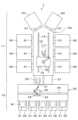
先ず、本実施形態にかかるウェハ処理装置について説明する。図1は、本実施形態にかかるウェハ処理装置1の構成の概略を示す平面図である。ウェハ処理装置1では、基板としてのウェハWに対して、例えばエッチング処理、成膜処理、拡散処理などの処理を行う。<Wafer Processing Device>
First, a wafer processing apparatus according to the present embodiment will be described. Fig. 1 is a plan view showing an outline of the configuration of a
図1に示すようにウェハ処理装置1は、大気部10と減圧部11がロードロックモジュール20、21を介して一体に接続された構成を有している。大気部10は、大気圧雰囲気下においてウェハWに所望の処理を行う大気モジュールを備える。減圧部11は、減圧雰囲気下においてウェハWに所望の処理を行う減圧モジュールを備える。As shown in FIG. 1, the
ロードロックモジュール20、21は、ゲートバルブ(図示せず)を介して、大気部10の後述するローダモジュール30と、減圧部11の後述するトランスファモジュール50を連結するように設けられている。ロードロックモジュール20、21は、ウェハWを一時的に保持するように構成されている。また、ロードロックモジュール20、21は、内部を大気圧雰囲気と減圧雰囲気(真空状態)とに切り替えられるように構成されている。The
大気部10は、後述するウェハ搬送機構40を備えたローダモジュール30と、複数のウェハWを保管可能なフープ31を載置するロードポート32とを有している。なお、ローダモジュール30には、ウェハWの水平方向の向きを調節するオリエンタモジュール(図示せず)や複数のウェハWを格納する格納モジュール(図示せず)などが隣接して設けられていてもよい。The
ローダモジュール30は内部が矩形の筐体からなり、筐体の内部は大気圧雰囲気に維持されている。ローダモジュール30の筐体の長辺を構成する一側面には、複数、例えば5つのロードポート32が並設されている。ローダモジュール30の筐体の長辺を構成する他側面には、ロードロックモジュール20、21が並設されている。The
ローダモジュール30の内部には、ウェハWを搬送するウェハ搬送機構40が設けられている。ウェハ搬送機構40は、ウェハWを保持して移動する搬送アーム41と、搬送アーム41を回転可能に支持する回転台42と、回転台42を搭載した回転載置台43とを有している。また、ローダモジュール30の内部には、ローダモジュール30の長手方向に延伸するガイドレール44が設けられている。回転載置台43はガイドレール44上に設けられ、ウェハ搬送機構40はガイドレール44に沿って移動可能に構成されている。Inside the
減圧部11は、ウェハWを同時に搬送するトランスファモジュール50と、トランスファモジュール50から搬送されたウェハWに所望の処理を行う処理モジュール60を有している。トランスファモジュール50及び処理モジュール60の内部はそれぞれ、減圧雰囲気に維持される。1つのトランスファモジュール50に対し、処理モジュール60は複数、例えば8つ設けられている。なお、処理モジュール60の数や配置は本実施形態に限定されず、任意に設定することができる。The
トランスファモジュール50は内部が多角形状(図示の例では五角形状)の筐体からなり、上述したようにロードロックモジュール20、21に接続されている。トランスファモジュール50は、ロードロックモジュール20に搬入されたウェハWを一の処理モジュール60に搬送して所望の処理を施した後、ロードロックモジュール21を介して大気部10に搬出する。The
処理モジュール60は、例えばエッチング処理、成膜処理、拡散処理などの処理を行う。処理モジュール60には、ウェハ処理の目的に応じた処理を行うモジュールを任意に選択することができる。また、処理モジュール60は、ゲートバルブ61を介してトランスファモジュール50に接続されている。なお、この処理モジュール60の構成は後述する。The
トランスファモジュール50の内部には、ウェハWを搬送するウェハ搬送機構70が設けられている。ウェハ搬送機構70は、ウェハWを保持して移動する搬送アーム71と、搬送アーム71を回転可能に支持する回転台72と、回転台72を搭載した回転載置台73とを有している。また、トランスファモジュール50の内部には、トランスファモジュール50の長手方向に延伸するガイドレール74が設けられている。回転載置台73はガイドレール74上に設けられ、ウェハ搬送機構70はガイドレール74に沿って移動可能に構成されている。Inside the
トランスファモジュール50では、ロードロックモジュール20に保持されたウェハWを搬送アーム71で受け取り、処理モジュール60に搬送する。また、所望の処理が施されたウェハWを搬送アーム71が保持し、ロードロックモジュール21に搬出する。In the
次に、以上のように構成されたウェハ処理装置1を用いて行われるウェハ処理について説明する。Next, we will explain the wafer processing performed using the
先ず、複数のウェハWを収納したフープ31がロードポート32に載置される。First, a
次に、ウェハ搬送機構40によって、フープ31からウェハWが取り出され、ロードロックモジュール20に搬入される。ロードロックモジュール20にウェハWが搬入されると、ロードロックモジュール20内が密閉され、減圧される。その後、ロードロックモジュール20の内部とトランスファモジュール50の内部が連通される。Next, the wafer W is removed from the
次に、ウェハ搬送機構70によってウェハWが保持され、ロードロックモジュール20からトランスファモジュール50に搬送される。Next, the wafer W is held by the
次に、ゲートバルブ61が開放され、ウェハ搬送機構70によって処理モジュール60にウェハWが搬入される。その後、ゲートバルブ61が閉じられ、処理モジュール60においてウェハWに所望の処理が行われる。なお、このウェハWに対する処理については後述する。Next, the
次に、ゲートバルブ61が開放され、ウェハ搬送機構70によって処理モジュール60からウェハWが搬出される。その後、ゲートバルブ61が閉じられる。Next, the
次に、ウェハ搬送機構70によって、ロードロックモジュール21にウェハWが搬入される。ロードロックモジュール21にウェハWが搬入されると、ロードロックモジュール21内が密閉され、大気開放される。その後、ロードロックモジュール21の内部とローダモジュール30の内部が連通される。Next, the wafer W is loaded into the
次に、ウェハ搬送機構40によってウェハWが保持され、ロードロックモジュール21からローダモジュール30を介してフープ31に戻されて収容される。こうして、ウェハ処理装置1における一連のウェハ処理が終了する。Next, the wafer W is held by the
<処理モジュール>
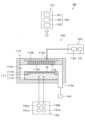
次に、上述した処理モジュール60について説明する。図2は、処理モジュール60の構成の概略を示す縦断面図である。<Processing Module>
Next, a description will be given of the above-mentioned
図2に示すように処理モジュール60は、プラズマ処理装置100及び制御部101を含む。プラズマ処理装置100は、プラズマ処理チャンバ110、ガス供給部120、RF(Radio Frequency:高周波)電力供給部130及び排気システム140を含む。また、プラズマ処理装置100は、支持部111及び上部電極シャワーヘッド112を含む。支持部111は、プラズマ処理チャンバ110内のプラズマ処理空間110sの下部領域に配置される。上部電極シャワーヘッド112は、支持部111の上方に配置され、プラズマ処理チャンバ110の天部(ceiling)の一部として機能し得る。As shown in FIG. 2, the
支持部111は、プラズマ処理空間110sにおいてウェハWを支持するように構成される。一実施形態において、支持部111は、下部電極113、載置台としての静電チャック114、及びエッジリング115を含む。静電チャック114は、下部電極113上に配置され、静電チャック114の上面でウェハWを支持するように構成される。エッジリング115は、下部電極113の周縁部上面においてウェハWを囲むように配置される。また、図示は省略するが、一実施形態において、支持部111は、当該支持部111を貫通し、ウェハWの下面に当接して昇降自在に構成されたリフタピンを含んでいてもよい。さらに、図示は省略するが、一実施形態において、支持部111は、静電チャック114及びウェハWのうち少なくとも1つをターゲット温度に調節するように構成される温調モジュールを含んでもよい。温調モジュールは、ヒータ、流路、又はこれらの組み合わせを含んでもよい。流路には、冷媒、伝熱ガスのような温調流体が流れる。The
上部電極シャワーヘッド112は、ガス供給部120からの1又はそれ以上の処理ガスをプラズマ処理空間110sに供給するように構成される。一実施形態において、上部電極シャワーヘッド112は、ガス入口112a、ガス拡散室112b、及び複数のガス出口112cを有する。ガス入口112aは、ガス供給部120及びガス拡散室112bと流体連通している。複数のガス出口112cは、ガス拡散室112b及びプラズマ処理空間110sと流体連通している。一実施形態において、上部電極シャワーヘッド112は、1又はそれ以上の処理ガスをガス入口112aからガス拡散室112b及び複数のガス出口112cを介してプラズマ処理空間110sに供給するように構成される。The
ガス供給部120は、1又はそれ以上のガスソース121及び1又はそれ以上の流量制御器122を含んでもよい。一実施形態において、ガス供給部120は、1又はそれ以上の処理ガスを、それぞれに対応のガスソース121からそれぞれに対応の流量制御器122を介してガス入口112aに供給するように構成される。各流量制御器122は、例えばマスフローコントローラ又は圧力制御式の流量制御器を含んでもよい。さらに、ガス供給部120は、1又はそれ以上の処理ガスの流量を変調又はパルス化する1又はそれ以上の流量変調デバイスを含んでもよい。The
RF電力供給部130は、RF電力、例えば1又はそれ以上のRF信号を、下部電極113、上部電極シャワーヘッド112、又は、下部電極113及び上部電極シャワーヘッド112の双方のような1又はそれ以上の電極に供給するように構成される。これにより、プラズマ処理空間110sに供給された1又はそれ以上の処理ガスからプラズマが生成される。したがって、RF電力供給部130は、プラズマ処理チャンバにおいて1又はそれ以上の処理ガスからプラズマを生成するように構成されるプラズマ生成部の少なくとも一部として機能し得る。一実施形態において、RF電力供給部130は、2つのRF生成部131a、131b及び2つの整合回路132a、132bを含む。一実施形態において、RF電力供給部130は、第1のRF信号を第1のRF生成部131aから第1の整合回路132aを介して下部電極113に供給するように構成される。例えば、第1のRF信号は、27MHz~100MHzの範囲内の周波数を有してもよい。The
また、一実施形態において、RF電力供給部130は、第2のRF信号を第2のRF生成部131bから第2の整合回路132bを介して下部電極113に供給するように構成される。例えば、第2のRF信号は、400kHz~13.56MHzの範囲内の周波数を有してもよい。代わりに、第2のRF生成部131bに代えて、DC(Direct Current)パルス生成部を用いてもよい。In one embodiment, the RF
さらに、図示は省略するが、本開示においては他の実施形態が考えられる。例えば、代替実施形態において、RF電力供給部130は、第1のRF信号をRF生成部から下部電極113に供給し、第2のRF信号を他のRF生成部から下部電極113に供給し、第3のRF信号をさらに他のRF生成部から下部電極113に供給するように構成されてもよい。加えて、他の代替実施形態において、DC電圧が上部電極シャワーヘッド112に印加されてもよい。Furthermore, although not shown, other embodiments are contemplated in the present disclosure. For example, in an alternative embodiment, the
またさらに、種々の実施形態において、1又はそれ以上のRF信号(すなわち、第1のRF信号、第2のRF信号等)の振幅がパルス化又は変調されてもよい。振幅変調は、オン状態とオフ状態との間、あるいは、2又はそれ以上の異なるオン状態の間でRF信号振幅をパルス化することを含んでもよい。Still further, in various embodiments, one or more RF signals (i.e., the first RF signal, the second RF signal, etc.) may be pulsed or modulated in amplitude. Amplitude modulation may include pulsing the RF signal amplitude between an on state and an off state, or between two or more different on states.
排気システム140は、例えばプラズマ処理チャンバ110の底部に設けられた排気口110eに接続され得る。排気システム140は、圧力弁及び真空ポンプを含んでもよい。真空ポンプは、ターボ分子ポンプ、粗引きポンプ又はこれらの組み合わせを含んでもよい。The exhaust system 140 may be connected to an
一実施形態において、制御部101は、本開示において述べられる種々の工程をプラズマ処理装置100に実行させるコンピュータ実行可能な命令を処理する。制御部101は、ここで述べられる種々の工程を実行するようにプラズマ処理装置100の各要素を制御するように構成され得る。一実施形態において、制御部101の一部又は全てがプラズマ処理装置100に含まれてもよい。制御部101は、例えばコンピュータ150を含んでもよい。コンピュータ150は、例えば、処理部(CPU:Central Processing Unit)151、記憶部152、及び通信インターフェース153を含んでもよい。処理部151は、記憶部152に格納されたプログラムに基づいて種々の制御動作を行うように構成され得る。記憶部152は、RAM(Random Access Memory)、ROM(Read Only Memory)、HDD(Hard Disk Drive)、SSD(Solid State Drive)、又はこれらの組み合わせを含んでもよい。通信インターフェース153は、LAN(Local Area Network)等の通信回線を介してプラズマ処理装置100との間で通信してもよい。In one embodiment, the
以上、種々の例示的実施形態について説明してきたが、上述した例示的実施形態に限定されることなく、様々な追加、省略、置換、及び変更がなされてもよい。また、異なる実施形態における要素を組み合わせて他の実施形態を形成することが可能である。Although various exemplary embodiments have been described above, various additions, omissions, substitutions, and modifications may be made without being limited to the exemplary embodiments described above. In addition, elements in different embodiments may be combined to form other embodiments.
<ウェハ処理>
次に、以上のように構成された処理モジュール60を用いて行われるウェハ処理について説明する。なお、処理モジュール60では、ウェハWに対して、例えばエッチング処理、成膜処理、拡散処理などの処理を行う。<Wafer Processing>
Next, a description will be given of wafer processing performed using the
先ず、プラズマ処理チャンバ110の内部にウェハWを搬入し、リフタピンの昇降により静電チャック114上にウェハWを載置する。その後、静電チャック114の電極に直流電圧を印加することにより、ウェハWはクーロン力によって静電チャック114に静電吸着され、保持される。また、ウェハWの搬入後、排気システム140によってプラズマ処理チャンバ110の内部を所定の真空度まで減圧する。First, the wafer W is loaded into the
次に、ガス供給部120から上部電極シャワーヘッド112を介してプラズマ処理空間110sに処理ガスを供給する。また、RF電力供給部130によりプラズマ生成用の高周波電力HFを下部電極113に供給し、処理ガスを励起させて、プラズマを生成する。この際、RF電力供給部130によりイオン引き込み用の高周波電力LFを供給してもよい。そして、生成されたプラズマの作用によって、ウェハWにプラズマ処理が施される。Next, the
なお、プラズマ処理中、温調モジュールによって、静電チャック114に吸着保持されたウェハWの温度を調整する。この際、ウェハWに熱を効率よく伝達させるために、静電チャック114の上面に吸着されたウェハWの裏面に向けて、HeガスやArガス等の伝熱ガスを供給する。During plasma processing, the temperature of the wafer W attracted and held on the
プラズマ処理を終了する際には、先ず、RF電力供給部130からの高周波電力HFの供給およびガス供給部120による処理ガスの供給を停止する。また、プラズマ処理中に高周波電力LFを供給していた場合には、当該高周波電力LFの供給も停止する。次いで、ウェハWの裏面への伝熱ガスの供給を停止し、静電チャック114によるウェハWの吸着保持を停止する。When plasma processing is terminated, first, the supply of high frequency power HF from the RF
その後、リフタピンによりウェハWを上昇させ、静電チャック114からウェハWを離脱させる。この離脱の際には、ウェハWの除電処理を行ってもよい。そして、プラズマ処理チャンバ110からウェハWを搬出して、ウェハWに対する一連のプラズマ処理が終了する。Then, the wafer W is raised by the lifter pins, and the wafer W is detached from the
<評価用ウェハ>
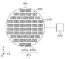
上述した実施形態において、ウェハ処理をウェハ面内で均一に行うためには、ウェハWの表面における処理ガスの流れを適切に制御することが肝要である。そこで、ガス流の評価をするためのウェハWe(以下、「評価用ウェハWe」という。)を用いて、処理ガスの流れの大きさ及び向きを測定する。図3は、本実施形態にかかる評価用ウェハWeの構成の概略を示す平面図である。<Evaluation wafer>
In the above-described embodiment, in order to perform wafer processing uniformly across the wafer surface, it is essential to appropriately control the flow of the process gas on the surface of the wafer W. Therefore, a wafer We for evaluating the gas flow (hereinafter, referred to as an "evaluation wafer We") is used to measure the magnitude and direction of the process gas flow. Fig. 3 is a plan view showing an outline of the configuration of the evaluation wafer We according to this embodiment.
図3に示すように評価用ウェハWeの表面には、複数のフローセンサ200が設けられている。フローセンサ200には、例えばMEMS(Micro Electro Mechanical Systems)センサが用いられる。MEMSセンサは薄型かつ小型であるため、評価用ウェハWeにフローセンサ200を多数設置することができる。As shown in FIG. 3, a plurality of
図4に示すようにMEMSセンサであるフローセンサ200は、サーマルセンサであり、ヒータ201、一対のサーモパイル202a、202b、及び温度センサ203を備える。一対のサーモパイル202a、202bは、ヒータ201を挟んで対称に配置されている。温度センサ203は、フローセンサ200の周囲の温度を測定する。As shown in FIG. 4, the
かかるフローセンサ200では、ガスの流れがない状態では、ヒータ201を中心としたサーモパイル202a、202bの温度分布が対称となる。一方、ガスの流れがある状態では、ヒータ201の風上側のサーモパイル202aの温度が低く、風下側のサーモパイル202bの温度が高くなり、温度の平衡状態が崩れる。この温度差をサーモパイル202a、202bの起電力差として検出することで、ガスの流量を測定することができる。In such a
評価用ウェハWeには、2つのフローセンサ200、200が一対で設けられている。以下の説明において、一方のフローセンサ200を第1のフローセンサ200aといい、他方のフローセンサ200を第2のフローセンサ200bという。また、一対のフローセンサ200a、200bを、センサ対210という。A pair of two
第1のフローセンサ200aは、第1の方向(図4の例ではX軸方向)におけるガスの流量を測定する。すなわち第1のフローセンサ200aでは、ヒータ201及びサーモパイル202a、202bがX軸方向に並べて配置される。第2のフローセンサ200bは、第1の方向と垂直な第2の方向(図4の例ではY軸方向)におけるガスの流量を測定する。すなわち第2のフローセンサ200bでは、ヒータ201及びサーモパイル202a、202bがY軸方向に並べて配置される。なお、図4中の矢印はガスの流れを示している。The
このようにセンサ対210では、第1のフローセンサ200aと第2のフローセンサ200bがそれぞれ直交する方向のガスの流量を測定する。そして、第1のフローセンサ200aと第2のフローセンサ200bの測定結果(ガス流のベクトル)を合成することで、センサ対210が設けられた位置におけるガスの流れの大きさ(流量)と方向を測定することが可能となる。In this way, in the
図3に示すように評価用ウェハWeには、その表面全面において、上述したセンサ対210が複数対形成されている。そして、各センサ対210がガス流の大きさ及び方向を測定する。各センサ対210の測定結果は、出力部220に出力される。この出力形式は特に限定されるものではないが、例えば無線LANが用いられる。出力部220では、各センサ対210が測定したガス流の大きさ及び方向を可視化する。そして、評価用ウェハWeの表面におけるガス流を把握することができる。As shown in FIG. 3, the evaluation wafer We has multiple pairs of the above-mentioned sensor pairs 210 formed over the entire surface thereof. Each
<ガス流測定方法>
次に、上述した処理モジュール60における、評価用ウェハWeを用いた処理ガスの流れの測定方法について説明する。<Gas flow measurement method>
Next, a method for measuring the flow of the process gas in the above-mentioned
先ず、プラズマ処理チャンバ110の内部に評価用ウェハWeを搬入し、リフタピンの昇降により静電チャック114上に評価用ウェハWeを載置する。その後、静電チャック114の電極に直流電圧を印加することにより、評価用ウェハWeはクーロン力によって静電チャック114に静電吸着され、保持される。また、評価用ウェハWeの搬入後、排気システム140によってプラズマ処理チャンバ110の内部を所定の真空度まで減圧する。First, the evaluation wafer We is loaded into the
次に、ガス供給部120から上部電極シャワーヘッド112を介してプラズマ処理空間110sに処理ガスを供給する。評価用ウェハWeでは、複数のフローセンサ200(複数対のセンサ対210)によって、評価用ウェハWeの表面における処理ガスの流れの大きさ及び向きが測定される。なお、この際、下部電極113には高周波電力が印加されず、すなわちプラズマは生成されない。Next, processing gas is supplied from the
フローセンサ200による測定結果は、出力部220に出力される。出力部220では、処理ガスの流れ及び大きさが可視化される。図5は、評価用ウェハWeにおける処理ガスの流れを示す一例である。図5において、矢印が処理ガスの流れの向きFを示し、矢印の大きさが処理ガスの大きさ(流量)を示し、矢印の向きが処理ガスの向きを示している。The measurement results from the
処理ガスの流れの測定が終了すると、ガス供給部120による処理ガスの供給を停止する。次いで、静電チャック114による評価用ウェハWeの吸着保持を停止する。When the measurement of the process gas flow is completed, the supply of process gas by the
その後、リフタピンにより評価用ウェハWeを上昇させ、静電チャック114から評価用ウェハWeを離脱させる。この離脱の際には、ウェハWの除電処理を行ってもよい。そして、プラズマ処理チャンバ110から評価用ウェハWeを搬出して、一連の処理ガスの流れの測定が終了する。Then, the evaluation wafer We is raised by the lifter pins and detached from the
以上の実施形態によれば、複数のフローセンサ200(複数対のセンサ対210)を用いて、評価用ウェハWeにおける処理ガスの流れの大きさ及び向きを適切に測定することができる。このように処理ガスの流れを把握できると、例えば、製品用のウェハWに処理を行う際に、ウェハ面内で処理ガスが適切に流れるように、当該処理ガスを制御することができる。その結果、ウェハWに対して所望の処理を面内均一に適切に行うことができる。また、ウェハ面内で処理ガスが極小的に高濃度になるように、当該処理ガスを制御することもできる。その結果、ウェハWに対する処理において局所的に生じた不具合を改善することも可能である。いずれの場合も、処理モジュール60における各部材(ハード)の形状や寸法などを最適化できる。According to the above embodiment, the magnitude and direction of the flow of the process gas in the evaluation wafer We can be appropriately measured using multiple flow sensors 200 (multiple pairs of sensors 210). If the flow of the process gas can be grasped in this way, for example, when processing a product wafer W, the process gas can be controlled so that the process gas flows appropriately within the wafer surface. As a result, the desired process can be appropriately performed on the wafer W uniformly within the surface. In addition, the process gas can be controlled so that the process gas is minimally concentrated within the wafer surface. As a result, it is possible to improve localized defects in the processing of the wafer W. In either case, the shape and dimensions of each component (hardware) in the
また、製品用のウェハWに処理を行う前後で、処理ガスの流れの大きさ及び向きを測定し、これらの測定結果を比較することで、トラブルが生じた際の原因を究明することができる。具体的には例えば、一の処理モジュール60において、製品用のウェハWに処理を行う前に、処理ガスの流れの大きさ及び向きの初期値を測定する。その後。製品用のウェハWに処理を行った後、処理ガスの流れの大きさ及び向きを測定する。そして、処理(プロセス)前に測定した初期値と、処理後に測定した測定結果を比較することで、トラブルの原因を究明することができる。しかも、従来のようにトライアンドエラーを繰り返す必要がなく、早期にトラブルの原因を特定することが可能となる。In addition, by measuring the magnitude and direction of the process gas flow before and after processing the product wafer W, and comparing these measurement results, the cause of any trouble that may occur can be identified. Specifically, for example, in one
トラブルの原因は、例えばプラズマ処理チャンバ110に付着物が付着する場合や、上部電極シャワーヘッド112のガス出口112cが詰まる場合など、種々存在する。プラズマ処理チャンバ110のトラブルの場合と上部電極シャワーヘッド112のトラブルの場合では、評価用ウェハWeにおける処理ガスの流れ方が異なる。そこで、本実施形態では、処理ガスの流れ方を測定することで、トラブルの原因を特定することができる。なお、トラブルの原因究明には、処理ガスの流れだけでなく、例えばトラブル発生時のエッチングレートなど、他のデータを用いてもよい。There are various causes of trouble, such as adhesion of deposits to the
また、フローセンサ200として、MEMSセンサなどの比熱の影響受けるセンサを用いた場合、処理モジュール60内のガス成分が変化すると、フローセンサ200からの出力が変動する。例えば、処理ガスに、前工程における残留ガスや処理モジュール60内に堆積した反応生成物から発生したガスなどが混入すると、混入したガスの比熱に応じてフローセンサ200からの出力が変動する。したがって、ウェハWの処理に異常が生じた場合に、そのときのフローセンサ200からの出力と、処理モジュール60内に処理ガスのみを流した場合の出力とを比較することで、混入したガスの種類などを特定することができる。In addition, when a sensor that is affected by specific heat, such as a MEMS sensor, is used as the
<他の実施形態>
評価用ウェハWeにおいて、フローセンサ200の配置や数は、図3に示した例に限定されない。例えば図6に示すように、評価用ウェハWeの同心円周上に、複数のセンサ対210が等間隔で配置されていてもよい。かかる場合であっても、センサ対210が設けられた位置における処理ガスの大きさ及び向きを測定することができるので、評価用ウェハWeの表面におけるガス流を測定することができる。<Other embodiments>
In the evaluation wafer We, the arrangement and number of the
また、処理モジュール60に評価用ウェハWeを搬送する際に、複数のフローセンサ200を用いて、評価用ウェハWeの表面におけるガスの流れの大きさ及び向きを測定してもよい。In addition, when the evaluation wafer We is transported to the
ウェハ処理装置1において、トランスファモジュール50の内部の圧力は、処理モジュール60の内部の圧力に比べて高くなっている。例えば処理モジュール60においてエッチング処理を行う場合、プラズマ処理チャンバ110の内部にはパーティクルが生じるが、トランスファモジュール50を陽圧にすることで、このパーティクルがトランスファモジュール50に流出するのを抑制する。かかる場合、評価用ウェハWeを処理モジュール60に搬入する際、ゲートバルブ61を開放すると、トランスファモジュール50から処理モジュール60に一方向のガスの流れが生じる。In the
ここで、評価用ウェハWeを処理モジュール60に搬入する際、その搬送速度によっては、トランスファモジュール50から処理モジュール60に向かうガスの流れに乱れや対流が生じるおそれがある。そこで、評価用ウェハWeを処理モジュール60に搬入する際、複数のフローセンサ200を用いて、表面のガスの流れの大きさ及び向きを測定する。そして、評価用ウェハWeの搬送速度を変動させ、また搬送速度の加速度を変動させて、図7に示すようにトランスファモジュール50から処理モジュール60に一方向のガスの流れFが生じるように、これら搬送速度と加速度を最適化する。Here, when the evaluation wafer We is loaded into the
以上のように、評価用ウェハWeを処理モジュール60に搬入する際の搬送速度と加速度を最適化することで、ガスの流れを適正化し、処理モジュール60の内部のパーティクルがトランスファモジュール50に流出するのを抑制することができる。As described above, by optimizing the transport speed and acceleration when loading the evaluation wafer We into the
なお、評価用ウェハWeを処理モジュール60から搬出する際にも同様に、評価用ウェハWeの表面におけるガスの流れの大きさ及び向きを測定し、搬送速度と加速度を最適化することができる。Similarly, when the evaluation wafer We is transported out of the
一方で、大量のガスがトランスファモジュール50から処理モジュール60に流れると、処理モジュール60の内部の雰囲気コンディションを変えるおそれがある。かかる場合、処理モジュール60で処理を行う前に内部雰囲気を調整するのに時間がかかる。そこで、このガスの流量も考慮して、評価用ウェハWeの搬送速度と加速度を最適化することで、処理モジュール60の雰囲気を維持し、ウェハ処理のスループットを向上させることができる。On the other hand, if a large amount of gas flows from the
以上の実施形態では、評価用ウェハWeの表面におけるガスの流れの大きさ及び向きを測定したが、製品用のウェハWの表面に複数のフローセンサ200を設けて、当該ウェハWの表面におけるガスの流れの大きさ及び向きを測定してもよい。かかる場合、処理モジュール60においてウェハWを処理する際には、測定結果に基づいて、リアルタイムで処理ガスの流れを制御することができる。また、トランスファモジュール50と処理モジュール60との間でウェハWを搬送する際には、測定結果に基づいて、リアルタイムで搬送速度と加速度を最適化することができる。In the above embodiment, the magnitude and direction of the gas flow on the surface of the evaluation wafer We were measured, but
また、以上の実施形態では、評価用ウェハWeの表面に複数のフローセンサ200を設けたが、処理モジュール60における各部材にフローセンサ200(センサ対210)を設けてもよい。例えばプラズマ処理チャンバ110の内側面、上部電極シャワーヘッド112の下面、静電チャック114の上面、エッジリング115の上面などに、フローセンサ200(センサ対210)を設けてもよい。かかる場合、処理モジュール60の内部における処理ガスの流れの大きさ及び向きも測定することができる。In the above embodiment,
以上の実施形態では、フローセンサ200としてMEMSセンサを用いたが、これに限定されない。ガスの流量を測定できるセンサであれば任意のフローセンサを用いることができる。In the above embodiment, a MEMS sensor is used as the
以上の実施形態では、処理モジュール60においてエッチング処理、成膜処理、拡散処理などの処理を行ったが、本開示の評価用ウェハWeとガス流測定方法は、ガスを用いたウェハ処理であれば他の処理にも適用することができる。In the above embodiment, processes such as etching, film formation, and diffusion were performed in the
今回開示された実施形態はすべての点で例示であって制限的なものではないと考えられるべきである。上記の実施形態は、添付の請求の範囲及びその主旨を逸脱することなく、様々な形態で省略、置換、変更されてもよい。The embodiments disclosed herein should be considered in all respects as illustrative and not restrictive. The above-described embodiments may be omitted, substituted, or modified in various ways without departing from the scope and spirit of the appended claims.
1 ウェハ処理装置
60 処理モジュール
101 制御部
110 プラズマ処理チャンバ
114 静電チャック
120 ガス供給部
200 フローセンサ
W ウェハ
We 評価用ウェハ REFERENCE SIGNS
Claims (11)
Translated fromJapanese(b)前記チャンバの内部に処理ガスを供給する工程と、
(c)前記複数のフローセンサを用いて前記基板の表面における前記処理ガスの流れの大きさ及び向きを測定する工程と、
(d)製品用基板に処理を行う工程と、
(e)前記工程(a)~(c)を行い、前記処理ガスの流れの大きさ及び向きを評価する工程と、
を含み、
前記工程(e)は、
(e1)前記工程(d)の前に、前記工程(a)~(c)を行い、前記処理ガスの流れの大きさ及び向きの初期値を測定する工程と、
(e2)前記工程(d)の後に、前記工程(a)~(c)を行う工程と、
(e3)前記工程(e1)で測定した初期値と、前記工程(e2)の測定結果とを比較する工程と、
を備える、基板処理方法。(a) placing a substrate having a plurality of flow sensors on a surface thereof on a stage provided inside a chamber;
(b) supplying a process gas into the chamber;
(c) measuring a magnitude and direction of flow of the process gas at a surface of the substrate using the plurality of flow sensors;
(d) subjecting the product substrate to processing;
(e) performing steps (a) to (c) and evaluating the magnitude and direction of the process gas flow;
Including,
The step (e)
(e1) performing steps (a) to (c) and measuring an initial value of the magnitude and direction of the flow of the process gas prior to step (d);
(e2) performing the steps (a) to (c) after the step (d);
(e3) comparing the initial value measured in the step (e1) with the measurement result of the step (e2);
A substrate processing method comprising:
前記工程(c)において、前記センサ対を用いて、当該センサ対が設けられた位置における前記処理ガスの大きさ及び向きを測定する、請求項1~3のいずれか一項に記載の基板処理方法。the plurality of flow sensors include a plurality of sensor pairs each including a first flow sensor for measuring a flow rate of the process gas in a first direction and a second flow sensor for measuring a flow rate of the process gas in a second direction perpendicular to the first direction;
4. The substrate processing method according to claim1 , wherein in the step (c), the sensor pair is used to measure a magnitude and a direction of the processing gas at a position where the sensor pair is provided.
(g)前記工程(a)~(c)を行い、前記フローセンサからの出力に基づき、前記処理ガスに含まれる成分を評価する工程と、
をさらに含み、
前記工程(g)は、
(g1)前記チャンバの内部に処理ガスのみを供給し、前記フローセンサの出力を測定する工程と、
(g2)前記処理ガスに、前記工程(f)における残留ガス又は前記チャンバの内部に堆積した反応生成物から発生したガスが混入した場合に、前記工程(a)~(c)を行い、前記フローセンサの出力を測定する工程と、
(g3)前記工程(g1)で測定した出力と、前記工程(g2)で測定した出力とを比較する工程と、
を備える、請求項1~6のいずれか一項に記載の基板処理方法。(f) subjecting the production substrate to processing;
(g) performing the steps (a) to (c) and evaluating components contained in the process gas based on an output from the flow sensor;
Further comprising:
The step (g)
(g1) supplying only a process gas into the chamber and measuring an output of the flow sensor;
(g2) performing steps (a) to (c) and measuring the output of the flow sensor whenthe processgas is contaminated with the residual gas from step (f) or the gas generated from the reaction product deposited inside the chamber ;
(g3) comparing the output measured in the step (g1) with the output measured in thestep (g2);
The substrate processing method according to claim1 , further comprising:
制御部と、
を備え、
前記制御部は、
(a)前記チャンバ内部に設けられた載置台に、表面に複数のフローセンサを有する基板を載置する工程と、
(b)前記チャンバの内部に処理ガスを供給する工程と、
(c)前記複数のフローセンサを用いて、前記基板の表面における前記処理ガスの流れの大きさ及び向きを測定する工程と、
(d)製品用基板に処理を行う工程と、
(e)前記工程(a)~(c)を行い、前記処理ガスの流れの大きさ及び向きを評価する工程と、
を含み、
前記工程(e)が、
(e1)前記工程(d)の前に、前記工程(a)~(c)を行い、前記処理ガスの流れの大きさ及び向きの初期値を測定する工程と、
(e2)前記工程(d)の後に、前記工程(a)~(c)を行う工程と、
(e3)前記工程(e1)で測定した初期値と、前記工程(e2)の測定結果とを比較する工程と、
を備える処理を実行するように装置を制御し、
前記フローセンサは、ヒータ、一対のサーモパイル及び温度センサを備え、
前記一対のサーモパイルは、前記ヒータを挟んで対称に配置されている、基板処理装置。a chamber having a gas inlet and a gas outlet;
A control unit;
Equipped with
The control unit is
(a) placing a substrate having a plurality of flow sensors on a surface thereof on a stage provided inside the chamber;
(b) supplying a process gas into the chamber;
(c) measuring a magnitude and direction of flow of the process gas at a surface of the substrate using the plurality of flow sensors;
(d) subjecting the product substrate to processing;
(e) performing steps (a) to (c) and evaluating the magnitude and direction of the process gas flow;
Including,
The step (e)
(e1) performing steps (a) to (c) and measuring an initial value of the magnitude and direction of the flow of the process gas prior to step (d);
(e2) performing the steps (a) to (c) after the step (d);
(e3) comparing the initial value measured in the step (e1) with the measurement result of the step (e2);
Controlling an apparatus to perform a processcomprising :
The flow sensor includes a heater, a pair of thermopiles, and a temperature sensor.
The pair of thermopiles are disposed symmetrically with respect to the heater.
前記複数対のセンサ対は、前記第1の方向と前記第2の方向に並べて配置されている、請求項9に記載の基板処理装置。the plurality of flow sensors include a plurality of sensor pairs each including a first flow sensor for measuring a flow rate of the process gas in a first direction and a second flow sensor for measuring a flow rate of the process gas in a second direction perpendicular to the first direction;
The substrate processing apparatus according to claim9 , wherein the plurality of sensor pairs are arranged side by side in the first direction and the second direction.
前記複数対のセンサ対は、前記基板の同心円周上に等間隔で配置されている、請求項9に記載の基板処理装置。
the plurality of flow sensors include a plurality of sensor pairs each including a first flow sensor for measuring a flow rate of the process gas in a first direction and a second flow sensor for measuring a flow rate of the process gas in a second direction perpendicular to the first direction;
The substrate processing apparatus according to claim9 , wherein the plurality of sensor pairs are arranged at equal intervals on a concentric circumference of the substrate.
Priority Applications (3)
| Application Number | Priority Date | Filing Date | Title |
|---|---|---|---|
| JP2020026160AJP7546364B2 (en) | 2020-02-19 | 2020-02-19 | Substrate processing method, substrate for evaluating gas flow, and substrate processing apparatus |
| CN202110179854.0ACN113284785B (en) | 2020-02-19 | 2021-02-09 | Substrate processing method, substrate for airflow evaluation, and substrate processing apparatus |
| US17/178,273US20210257197A1 (en) | 2020-02-19 | 2021-02-18 | Substrate processing method, gas flow evaluation substrate and substrate processing apparatus |
Applications Claiming Priority (1)
| Application Number | Priority Date | Filing Date | Title |
|---|---|---|---|
| JP2020026160AJP7546364B2 (en) | 2020-02-19 | 2020-02-19 | Substrate processing method, substrate for evaluating gas flow, and substrate processing apparatus |
Publications (2)
| Publication Number | Publication Date |
|---|---|
| JP2021132097A JP2021132097A (en) | 2021-09-09 |
| JP7546364B2true JP7546364B2 (en) | 2024-09-06 |
Family
ID=77273001
Family Applications (1)
| Application Number | Title | Priority Date | Filing Date |
|---|---|---|---|
| JP2020026160AActiveJP7546364B2 (en) | 2020-02-19 | 2020-02-19 | Substrate processing method, substrate for evaluating gas flow, and substrate processing apparatus |
Country Status (3)
| Country | Link |
|---|---|
| US (1) | US20210257197A1 (en) |
| JP (1) | JP7546364B2 (en) |
| CN (1) | CN113284785B (en) |
Families Citing this family (1)
| Publication number | Priority date | Publication date | Assignee | Title |
|---|---|---|---|---|
| KR102760072B1 (en)* | 2022-10-07 | 2025-01-24 | 도쿄엘렉트론가부시키가이샤 | Substrate processing system and method for mounting edge rings |
Citations (6)
| Publication number | Priority date | Publication date | Assignee | Title |
|---|---|---|---|---|
| JP2000150608A (en) | 1998-11-18 | 2000-05-30 | Hitachi Ltd | Semiconductor manufacturing method |
| JP2006505940A (en) | 2002-11-04 | 2006-02-16 | ブリオン テクノロジーズ,インコーポレーテッド | Method and apparatus for monitoring the manufacture of integrated circuits |
| JP2009064873A (en) | 2007-09-05 | 2009-03-26 | Hitachi High-Technologies Corp | Method for conveying object to be processed in semiconductor manufacturing apparatus |
| JP2013015376A (en) | 2011-07-01 | 2013-01-24 | Tokyo Electron Ltd | Data acquisition method of substrate processing device and substrate for sensor |
| JP2013167451A (en) | 2012-02-14 | 2013-08-29 | Tokyo Electron Ltd | Wind velocity measurement method and wind velocity measurement device |
| JP2019138780A (en) | 2018-02-10 | 2019-08-22 | 木村 光照 | Heat type flow sensor |
Family Cites Families (6)
| Publication number | Priority date | Publication date | Assignee | Title |
|---|---|---|---|---|
| US4254659A (en)* | 1979-01-12 | 1981-03-10 | Kbg Corporation | Fluid dynamic angular rate sensor |
| JP4594800B2 (en)* | 2005-06-02 | 2010-12-08 | 東京エレクトロン株式会社 | Substrate processing method, substrate processing program, and storage medium |
| JP6907518B2 (en)* | 2016-01-15 | 2021-07-21 | 東京エレクトロン株式会社 | Vacuum processing equipment and operation method of the vacuum processing equipment. |
| JP6951923B2 (en)* | 2017-09-27 | 2021-10-20 | 東京エレクトロン株式会社 | Substrate processing equipment, substrate processing method and computer storage medium |
| CN111377391B (en)* | 2018-12-27 | 2023-08-25 | 中芯集成电路(宁波)有限公司上海分公司 | MEMS packaging structure and manufacturing method thereof |
| CN215493946U (en)* | 2021-08-25 | 2022-01-11 | 江苏峰工电气科技有限公司 | High-voltage overhead line partial discharge accurate positioning device |
- 2020
- 2020-02-19JPJP2020026160Apatent/JP7546364B2/enactiveActive
- 2021
- 2021-02-09CNCN202110179854.0Apatent/CN113284785B/enactiveActive
- 2021-02-18USUS17/178,273patent/US20210257197A1/ennot_activeAbandoned
Patent Citations (6)
| Publication number | Priority date | Publication date | Assignee | Title |
|---|---|---|---|---|
| JP2000150608A (en) | 1998-11-18 | 2000-05-30 | Hitachi Ltd | Semiconductor manufacturing method |
| JP2006505940A (en) | 2002-11-04 | 2006-02-16 | ブリオン テクノロジーズ,インコーポレーテッド | Method and apparatus for monitoring the manufacture of integrated circuits |
| JP2009064873A (en) | 2007-09-05 | 2009-03-26 | Hitachi High-Technologies Corp | Method for conveying object to be processed in semiconductor manufacturing apparatus |
| JP2013015376A (en) | 2011-07-01 | 2013-01-24 | Tokyo Electron Ltd | Data acquisition method of substrate processing device and substrate for sensor |
| JP2013167451A (en) | 2012-02-14 | 2013-08-29 | Tokyo Electron Ltd | Wind velocity measurement method and wind velocity measurement device |
| JP2019138780A (en) | 2018-02-10 | 2019-08-22 | 木村 光照 | Heat type flow sensor |
Also Published As
| Publication number | Publication date |
|---|---|
| JP2021132097A (en) | 2021-09-09 |
| CN113284785B (en) | 2025-08-12 |
| CN113284785A (en) | 2021-08-20 |
| US20210257197A1 (en) | 2021-08-19 |
Similar Documents
| Publication | Publication Date | Title |
|---|---|---|
| US6553277B1 (en) | Method and apparatus for vacuum treatment | |
| JP7499142B2 (en) | Processing system and processing method | |
| US11715648B2 (en) | Substrate processing apparatus and substrate drying method | |
| US11804368B2 (en) | Cleaning method and plasma processing apparatus | |
| US11049743B2 (en) | Substrate processing apparatus, flow rate control method, and storage medium storing flow rate control program | |
| JP7546364B2 (en) | Substrate processing method, substrate for evaluating gas flow, and substrate processing apparatus | |
| JP7398306B2 (en) | Gas inspection method, substrate processing method and substrate processing system | |
| KR20180127763A (en) | Apparatus for treating substrate | |
| US7871471B2 (en) | Substrate processing apparatus inspection method and method for reducing quantity of particles on substrate | |
| US10748779B2 (en) | Substrate processing method | |
| JP4869551B2 (en) | Process control system and process control method | |
| US20230420286A1 (en) | Substrate processing apparatus and transfer method | |
| JP2007088497A (en) | Process control system, process control method and process processing device | |
| KR20080060853A (en) | Load lock chamber, substrate processing apparatus and substrate processing method | |
| KR20070012070A (en) | Semiconductor manufacturing equipment | |
| KR20180113470A (en) | System design for in-line particle and contamination metrology for showerhead and electrode parts | |
| JP2002296096A (en) | Processing method and processing device | |
| JP7550695B2 (en) | Stage inspection method | |
| KR102241600B1 (en) | Loadlock chamber and system for treating substrate with the loadlock chamber | |
| KR102867170B1 (en) | Processing system and processing method | |
| KR20240097573A (en) | Substrate treating apparatus and semiconductor manufacturing equipment including the same | |
| TW202503955A (en) | Cluster Tools | |
| KR20000055251A (en) | A method and an apparatus for positioning of a semiconductor wafer transfer equipment | |
| JP2010024487A (en) | Substrate treatment apparatus | |
| KR20070080771A (en) | Substrate Processing Apparatus and Method |
Legal Events
| Date | Code | Title | Description |
|---|---|---|---|
| A621 | Written request for application examination | Free format text:JAPANESE INTERMEDIATE CODE: A621 Effective date:20221122 | |
| A977 | Report on retrieval | Free format text:JAPANESE INTERMEDIATE CODE: A971007 Effective date:20230824 | |
| A131 | Notification of reasons for refusal | Free format text:JAPANESE INTERMEDIATE CODE: A131 Effective date:20230912 | |
| A521 | Request for written amendment filed | Free format text:JAPANESE INTERMEDIATE CODE: A523 Effective date:20231107 | |
| A131 | Notification of reasons for refusal | Free format text:JAPANESE INTERMEDIATE CODE: A131 Effective date:20240206 | |
| A521 | Request for written amendment filed | Free format text:JAPANESE INTERMEDIATE CODE: A523 Effective date:20240404 | |
| TRDD | Decision of grant or rejection written | ||
| A01 | Written decision to grant a patent or to grant a registration (utility model) | Free format text:JAPANESE INTERMEDIATE CODE: A01 Effective date:20240730 | |
| A61 | First payment of annual fees (during grant procedure) | Free format text:JAPANESE INTERMEDIATE CODE: A61 Effective date:20240827 | |
| R150 | Certificate of patent or registration of utility model | Ref document number:7546364 Country of ref document:JP Free format text:JAPANESE INTERMEDIATE CODE: R150 |