JP7545858B2 - Thermal printhead and method for manufacturing the same - Google Patents
Thermal printhead and method for manufacturing the sameDownload PDFInfo
- Publication number
- JP7545858B2 JP7545858B2JP2020171779AJP2020171779AJP7545858B2JP 7545858 B2JP7545858 B2JP 7545858B2JP 2020171779 AJP2020171779 AJP 2020171779AJP 2020171779 AJP2020171779 AJP 2020171779AJP 7545858 B2JP7545858 B2JP 7545858B2
- Authority
- JP
- Japan
- Prior art keywords
- heat storage
- layer
- storage layer
- thermal printhead
- glass paste
- Prior art date
- Legal status (The legal status is an assumption and is not a legal conclusion. Google has not performed a legal analysis and makes no representation as to the accuracy of the status listed.)
- Active
Links
- 238000000034methodMethods0.000titleclaimsdescription102
- 238000004519manufacturing processMethods0.000titleclaimsdescription61
- 239000011521glassSubstances0.000claimsdescription142
- 238000005338heat storageMethods0.000claimsdescription136
- 239000000758substrateSubstances0.000claimsdescription91
- 238000007639printingMethods0.000claimsdescription83
- 238000010304firingMethods0.000claimsdescription43
- 239000000463materialSubstances0.000claimsdescription42
- 238000011144upstream manufacturingMethods0.000claimsdescription22
- 238000001035dryingMethods0.000claimsdescription20
- 238000005530etchingMethods0.000claimsdescription18
- 239000004065semiconductorSubstances0.000claimsdescription18
- 239000013078crystalSubstances0.000claimsdescription17
- 239000002184metalSubstances0.000claimsdescription6
- 229910052751metalInorganic materials0.000claimsdescription6
- 238000002360preparation methodMethods0.000claimsdescription6
- 230000005611electricityEffects0.000claimsdescription4
- 239000010410layerSubstances0.000description239
- 239000010408filmSubstances0.000description28
- 244000126211Hericium coralloidesSpecies0.000description12
- VYPSYNLAJGMNEJ-UHFFFAOYSA-NSilicium dioxideChemical compoundO=[Si]=OVYPSYNLAJGMNEJ-UHFFFAOYSA-N0.000description12
- 239000011241protective layerSubstances0.000description11
- 230000015572biosynthetic processEffects0.000description10
- 238000010438heat treatmentMethods0.000description10
- 238000007650screen-printingMethods0.000description10
- 125000006850spacer groupChemical group0.000description10
- KWYUFKZDYYNOTN-UHFFFAOYSA-MPotassium hydroxideChemical compound[OH-].[K+]KWYUFKZDYYNOTN-UHFFFAOYSA-M0.000description9
- 229920005989resinPolymers0.000description8
- 239000011347resinSubstances0.000description8
- 239000010949copperSubstances0.000description6
- 230000017525heat dissipationEffects0.000description6
- 230000001681protective effectEffects0.000description6
- 239000000377silicon dioxideSubstances0.000description6
- 235000012239silicon dioxideNutrition0.000description6
- WGTYBPLFGIVFAS-UHFFFAOYSA-Mtetramethylammonium hydroxideChemical compound[OH-].C[N+](C)(C)CWGTYBPLFGIVFAS-UHFFFAOYSA-M0.000description6
- BOTDANWDWHJENH-UHFFFAOYSA-NTetraethyl orthosilicateChemical compoundCCO[Si](OCC)(OCC)OCCBOTDANWDWHJENH-UHFFFAOYSA-N0.000description5
- 239000007864aqueous solutionSubstances0.000description5
- 229910052681coesiteInorganic materials0.000description5
- 229910052906cristobaliteInorganic materials0.000description5
- 238000000151depositionMethods0.000description5
- 238000004544sputter depositionMethods0.000description5
- 229910052682stishoviteInorganic materials0.000description5
- 229910052905tridymiteInorganic materials0.000description5
- 229910052581Si3N4Inorganic materials0.000description4
- 229910004298SiO 2Inorganic materials0.000description4
- 239000000203mixtureSubstances0.000description4
- HQVNEWCFYHHQES-UHFFFAOYSA-Nsilicon nitrideChemical compoundN12[Si]34N5[Si]62N3[Si]51N64HQVNEWCFYHHQES-UHFFFAOYSA-N0.000description4
- 239000010936titaniumSubstances0.000description4
- 230000000694effectsEffects0.000description3
- 239000011810insulating materialSubstances0.000description3
- MZLGASXMSKOWSE-UHFFFAOYSA-Ntantalum nitrideChemical compound[Ta]#NMZLGASXMSKOWSE-UHFFFAOYSA-N0.000description3
- PMHQVHHXPFUNSP-UHFFFAOYSA-Mcopper(1+);methylsulfanylmethane;bromideChemical compoundBr[Cu].CSCPMHQVHHXPFUNSP-UHFFFAOYSA-M0.000description2
- 238000010030laminatingMethods0.000description2
- 230000001590oxidative effectEffects0.000description2
- 230000000149penetrating effectEffects0.000description2
- HBMJWWWQQXIZIP-UHFFFAOYSA-Nsilicon carbideChemical compound[Si+]#[C-]HBMJWWWQQXIZIP-UHFFFAOYSA-N0.000description2
- 229910010271silicon carbideInorganic materials0.000description2
- RYGMFSIKBFXOCR-UHFFFAOYSA-NCopperChemical compound[Cu]RYGMFSIKBFXOCR-UHFFFAOYSA-N0.000description1
- RTAQQCXQSZGOHL-UHFFFAOYSA-NTitaniumChemical compound[Ti]RTAQQCXQSZGOHL-UHFFFAOYSA-N0.000description1
- 229910052782aluminiumInorganic materials0.000description1
- XAGFODPZIPBFFR-UHFFFAOYSA-NaluminiumChemical compound[Al]XAGFODPZIPBFFR-UHFFFAOYSA-N0.000description1
- 229910052802copperInorganic materials0.000description1
- 238000005520cutting processMethods0.000description1
- 230000002542deteriorative effectEffects0.000description1
- 239000003822epoxy resinSubstances0.000description1
- 230000020169heat generationEffects0.000description1
- 239000007769metal materialSubstances0.000description1
- 230000002093peripheral effectEffects0.000description1
- 238000007747platingMethods0.000description1
- 229920000647polyepoxidePolymers0.000description1
- 238000003825pressingMethods0.000description1
- 239000002994raw materialSubstances0.000description1
- 229910052710siliconInorganic materials0.000description1
- 239000010703siliconSubstances0.000description1
- 239000010409thin filmSubstances0.000description1
- 229910052719titaniumInorganic materials0.000description1
Images


Landscapes
- Electronic Switches (AREA)
Description
Translated fromJapanese本開示は、サーマルプリントヘッド、および、サーマルプリントヘッドの製造方法に関する。This disclosure relates to a thermal printhead and a method for manufacturing a thermal printhead.
特許文献1には、従来のサーマルプリントヘッドの一例が開示されている。サーマルプリントヘッドは一般に、ヘッド基板上に主走査方向に並ぶ多数の発熱部を備えている。各発熱部は、蓄熱層を介してヘッド基板に形成された抵抗体層上に、抵抗体層の一部を露出させるように上流側導電層および下流側導電層を積層することで形成されている。上流側電極層と下流側電極層との間を通電することにより、上記抵抗体層の露出部(発熱部)がジュール熱により発熱する。蓄熱層は、発熱部が発する熱を蓄えるために形成され、高速印字を可能にしている。
特許文献1に開示されたサーマルプリントヘッドは、基材としてSi(シリコン)が用いられ、半導体プロセスにより、抵抗体層を含む各構成部が形成されている。この場合、蓄熱層は、SiO2(二酸化ケイ素)を用いたスパッタリングまたはCVD法により形成
される。スパッタリングなどの工程は、蓄熱層の必要な厚みに応じて、繰り返し行う必要がある。したがって、さらなる高速印字に必要な厚みの蓄熱層を形成するには相当な時間を要し、サーマルプリントヘッドの製造効率が悪化するという問題がある。加えて、サーマルプリントヘッドに対して消費電力の低減が要請されている。 The thermal printhead disclosed in
本開示は、上記した事情のもとで考え出されたものであって、基材と発熱部との間に、十分な厚みの蓄熱層を簡易に形成することができるサーマルプリントヘッドを提供すること、また、そのサーマルプリントヘッドの製造方法を提供することをその課題とする。The present disclosure was conceived in light of the above circumstances, and aims to provide a thermal printhead that can easily form a heat storage layer of sufficient thickness between the substrate and the heat generating portion, and to provide a method for manufacturing the thermal printhead.
本開示の第1の側面によって提供されるサーマルプリントヘッドは、厚さ方向の一方を向く主面を有し、単結晶半導体からなる基材と、前記主面の上に形成され且つ主走査方向に配列された複数の発熱部を含む抵抗体層と、前記基材と前記抵抗体層との間に形成された絶縁層と、前記基材と前記複数の発熱部との間に形成された蓄熱層とを備えており、前記蓄熱層は、ガラス材料からなるグレーズであり、前記蓄熱層の副走査方向の寸法に対する前記厚さ方向の寸法の比率は、0.05以上0.2以下である。The thermal printhead provided by the first aspect of the present disclosure comprises a substrate having a main surface facing in one direction in the thickness direction and made of a single crystal semiconductor, a resistor layer formed on the main surface and including a plurality of heat generating portions arranged in the main scanning direction, an insulating layer formed between the substrate and the resistor layer, and a heat storage layer formed between the substrate and the plurality of heat generating portions, the heat storage layer being a glaze made of a glass material, and the ratio of the thickness direction dimension of the heat storage layer to the sub-scanning direction dimension is 0.05 or more and 0.2 or less.
本開示の第2の側面によって提供されるサーマルプリントヘッドの製造方法は、単結晶半導体からなる基材を準備する準備工程と、前記基材の上に、第1ガラスペーストを配置する第1印刷工程と、前記第1ガラスペーストを焼成することで、第1グレーズを形成する第1グレーズ形成工程と、前記第1グレーズの上に、主走査方向に配列された複数の発熱部を形成する発熱部形成工程とを備えている。The method for manufacturing a thermal printhead provided by the second aspect of the present disclosure includes a preparation step of preparing a substrate made of a single crystal semiconductor, a first printing step of placing a first glass paste on the substrate, a first glaze forming step of forming a first glaze by firing the first glass paste, and a heating part forming step of forming a plurality of heating parts arranged in the main scanning direction on the first glaze.
本開示によれば、十分な厚みの蓄熱層を簡易に形成することができる。According to the present disclosure, it is possible to easily form a heat storage layer of sufficient thickness.
本開示のその他の特徴および利点は、添付図面を参照して以下に行う詳細な説明によって、より明らかとなろう。Other features and advantages of the present disclosure will become more apparent from the following detailed description taken in conjunction with the accompanying drawings.
以下、本開示の好ましい実施の形態につき、図面を参照して具体的に説明する。The preferred embodiment of this disclosure will be described in detail below with reference to the drawings.
本開示において、「ある物Aがある物Bに形成されている」および「ある物Aがある物B上に形成されている」とは、特段の断りのない限り、「ある物Aがある物Bに直接形成されていること」、および、「ある物Aとある物Bとの間に他の物を介在させつつ、ある物Aがある物Bに形成されていること」を含む。同様に、「ある物Aがある物Bに配置されている」および「ある物Aがある物B上に配置されている」とは、特段の断りのない限り、「ある物Aがある物Bに直接配置されていること」、および、「ある物Aとある物Bとの間に他の物を介在させつつ、ある物Aがある物Bに配置されていること」を含む。同様に、「ある物Aがある物B上に位置している」とは、特段の断りのない限り、「ある物Aがある物Bに接して、ある物Aがある物B上に位置していること」、および、「ある物Aとある物Bとの間に他の物が介在しつつ、ある物Aがある物B上に位置していること」を含む。また、「ある物Aがある物Bにある方向に見て重なる」とは、特段の断りのない限り、「ある物Aがある物Bのすべてに重なること」、および、「ある物Aがある物Bの一部に重なること」を含む。In this disclosure, "a certain object A is formed on a certain object B" and "a certain object A is formed on a certain object B" include "a certain object A is formed directly on a certain object B" and "a certain object A is formed on a certain object B with another object interposed between the certain object A and the certain object B" unless otherwise specified. Similarly, "a certain object A is disposed on a certain object B" and "a certain object A is disposed on a certain object B" include "a certain object A is disposed directly on a certain object B" and "a certain object A is disposed on a certain object B with another object interposed between the certain object A and the certain object B" unless otherwise specified. Similarly, "a certain object A is located on a certain object B" includes "a certain object A is located on a certain object B in contact with a certain object B" and "a certain object A is located on a certain object B with another object interposed between the certain object A and the certain object B". Additionally, unless otherwise specified, "an object A overlaps an object B when viewed in a certain direction" includes "an object A overlaps the entirety of an object B" and "an object A overlaps a part of an object B."
<第1実施形態>
図1~図6は、本開示の第1実施形態に係るサーマルプリントヘッドを示している。本実施形態のサーマルプリントヘッドA1は、ヘッド基板1、接続基板5、複数のワイヤ61,62、複数のドライバIC7、保護樹脂78および放熱部材8を備えている。サーマルプリントヘッドA1は、プラテンローラ99(図4参照)によって搬送される印刷媒体(図示略)に印刷を施すプリンタに組み込まれるものである。印刷媒体としては、たとえばバーコードシートやレシートを作成するための感熱紙が挙げられる。First Embodiment
1 to 6 show a thermal printhead according to a first embodiment of the present disclosure. The thermal printhead A1 of this embodiment comprises a
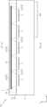
図1は、サーマルプリントヘッドA1を示す平面図である。図2は、サーマルプリントヘッドA1を示す要部拡大平面図である。図3は、サーマルプリントヘッドA1を示す要部拡大平面図である。図4は、図1のIV-IV線に沿う断面図である。図5は、サーマルプリントヘッドA1の要部断面図であり、図4の一部を拡大した断面図である。図6は、サーマルプリントヘッドA1の要部拡大断面図であり、図5の一部を拡大した断面図である。図1~図3においては、理解の便宜上、後述する保護層2を省略している。図1および図2においては、理解の便宜上、保護樹脂78を省略している。また、図2においては、理解の便宜上、ワイヤ61を省略している。また、これらの図において、ヘッド基板1の長手方向(主走査方向)をx方向とし、短手方向(副走査方向)をy方向とし、厚さ方向をz方向として説明する。また、y方向については、図1~図3の下方(図4~図6の右方)を印刷媒体が送られてくる「上流」とし、図1~図3の上方(図4~図6の左方)を印刷媒体が排出される「下流」とする。また、z方向については、図4~図6の上方(z方向を示す矢印が指す方向)を「上方」とし、その反対方向を「下方」とする。以下の図においても同様である。Figure 1 is a plan view of the thermal printhead A1. Figure 2 is an enlarged plan view of the thermal printhead A1. Figure 3 is an enlarged plan view of the thermal printhead A1. Figure 4 is a cross-sectional view taken along line IV-IV in Figure 1. Figure 5 is a cross-sectional view of the thermal printhead A1, which is an enlarged cross-sectional view of a portion of Figure 4. Figure 6 is a cross-sectional view of the thermal printhead A1, which is an enlarged cross-sectional view of a portion of Figure 5. For ease of understanding, the
図4に示すように、サーマルプリントヘッドA1において、ヘッド基板1および接続基板5は、放熱部材8上で、y方向に隣接して搭載されている。ヘッド基板1には、後に詳説する構成により、x方向に配列される複数の発熱部41が形成されている。この発熱部41は、接続基板5に搭載されたドライバIC7により選択的に発熱駆動され、コネクタ59を介して外部から送信される印字信号にしたがって、プラテンローラ99によって発熱部41に押圧される印刷媒体に印字を行う。As shown in FIG. 4, in the thermal printhead A1, the
ヘッド基板1は、図1~図6に示すように、基材10、蓄熱層15、絶縁層19、保護層2、電極層3、および、抵抗体層4を備えている。As shown in Figures 1 to 6, the
基材10は、単結晶半導体からなる。単結晶半導体としては、Siが好適である。基材10は、図1に示すように、z方向視において、x方向を長手方向とし、y方向を短手方向とする細長矩形状である。基材10の大きさは限定されないが、一例を挙げると、x方向の寸法は、たとえば20mm以上300mm以下、y方向の寸法は、たとえば1.0mm以上5.0mm以下、z方向の寸法は、たとえば725μmである。基材10において、y方向のドライバIC7に近い側が上流側であり、ドライバIC7から遠い側が下流側である。印刷媒体は、プラテンローラ99によって、y方向の上流側から下流側に搬送される。The
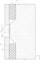
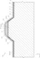
基材10は、図1、図2、図5および図6に示すように、主面11および凸部12を有している。主面11は、z方向の上方を向く。本開示では、主面11は、x-y平面(x方向とy方向で規定される平面、他の平面も同様)に沿って広がっており、x-y平面に略平行な平面である。主面11は、(100)面である。凸部12は、主面11からz方向に突出しており、x方向に延びている。凸部12は、主面11の下流側寄りに形成されている。凸部12は、y-z平面に沿う断面の形状が、x方向に一様である。以下では、y-z平面に沿う断面を「y-z断面」という。凸部12は、z方向下方側の端部におけるy方向の寸法W1が、たとえば500μmであり、z方向上方側の端部におけるy方向の寸法W2が、たとえば200μmである。また、凸部12のz方向の寸法H1は、たとえば150μmである。凸部12は、図6に示すように、頂部13および一対の傾斜部14を含んでいる。As shown in Figures 1, 2, 5 and 6, the
頂部13は、図5および図6に示すように、凸部12のうち、主面11からのz方向の距離が相対的に大きい部分である。頂部13は、主面11と平行な頂面131を有する。頂面131は、略平面である。頂面131は、z方向視において、x方向に長く延びる細長矩形状である。上記寸法H1は、頂面131と主面11とのz方向における離間距離である。As shown in Figures 5 and 6, the top 13 is a portion of the
一対の傾斜部14は、図5および図6に示すように、凸部12のうち、頂部13からy方向に離れるほど低位となるように主面11および頂面131に対して傾斜する部分である。一対の傾斜部14はそれぞれ、主面11と頂部13とに繋がり、y方向においてこれらに挟まれている。一対の傾斜部14には、頂部13に対して上流側の傾斜部14と下流側の傾斜部14とがある。一対の傾斜部14はそれぞれ、主面11および頂面131に対して傾斜した傾斜面141を有する。各傾斜面141は、略平面である。主面11に対する各傾斜面141の傾斜角α1は、たとえば54.7度である。各傾斜面141は、(111)面である。As shown in Figs. 5 and 6, the pair of
蓄熱層15は、たとえば非晶質ガラスなどのガラス材料からなるグレーズである。当該グレーズ(蓄熱層15)は、たとえばガラスペーストを焼成することにより形成される。本実施形態では、蓄熱層15の熱膨張係数は、基材10の材料であるSiと同程度である。なお、蓄熱層15のガラス材料の特性は限定されない。図5および図6に示すように、蓄熱層15は、凸部12の頂部13の上に配置されている。蓄熱層15は、頂面131に接しており、本実施形態では、蓄熱層15は、傾斜面141には接していない。蓄熱層15は、x方向に延びており、頂面131のy方向の全幅にわたって形成されている。The
本実施形態では、後述する製造方法に示すように、蓄熱層15は、孔版印刷(たとえばスクリーン印刷)によってガラスペーストを配置して焼成する工程を2回繰り返すことで形成される。具体的には、1回目の孔版印刷および焼成により、凸部12の頂部13の上にグレーズを形成する。そして、当該グレーズの上に、2回目の孔版印刷によってガラスペーストを配置する。2回目の孔版印刷では、グレーズの上にガラスペーストを配置するので、1回目の孔版印刷の場合よりz方向の寸法が大きくなるように(たとえば3倍程度)、ガラスペーストを配置できる。つまり、本実施形態では、蓄熱層15は、1回の孔版印刷および焼成によって形成される場合より、圧倒的に厚く(たとえば4倍程度)形成される。本実施形態では、2回目の孔版印刷で配置されるガラスペーストは、1回目の孔版印刷で配置されるガラスペーストと同じ組成のものである。したがって、蓄熱層15は、境界がなく一体となったグレーズになっている。なお、製造方法の詳細については後述する。In this embodiment, as shown in the manufacturing method described later, the
本実施形態では、蓄熱層15の厚さ(z方向の寸法H2)は、たとえば30μm以上200μm以下(好ましくは50μm以上60μm以下)である。また、蓄熱層15の幅(y方向の寸法W2)に対するz方向の寸法H2の比率(いわゆるアスペクト比)は、0.05以上0.2以下である。本実施形態では、蓄熱層15が頂面131のy方向の全幅にわたって形成されているので、蓄熱層15の幅は、頂面131の幅(y方向の寸法)、すなわち、凸部12のz方向上方側の端部におけるy方向の寸法W2と同じになっている。なお、蓄熱層15の各寸法は限定されない。蓄熱層15は、充分に蓄熱が可能であり、かつ、不必要に蓄熱し過ぎないように、厚さ(寸法H2)および幅(寸法W2)が設計される。蓄熱層15は、必要な厚さ(またはアスペクト比)が小さい場合は、1回の孔版印刷および焼成により形成されてもよい。また、蓄熱層15は、必要な厚さ(またはアスペクト比率)が形成できるのであれば、孔版印刷以外の方法(たとえばディスペンサーによるガラスペーストの塗布など)を用いてもよい。In this embodiment, the thickness (z-direction dimension H2) of the
図6に示すように、蓄熱層15には、その上面において、y方向両端に一対のラウンド部151が形成されている。一対のラウンド部151はそれぞれ、盛り上がるように湾曲した部分である。一対のラウンド部151により、蓄熱層15の表面が、一対の傾斜部14(凸部12)の各傾斜面141にかけて滑らかに連続させられている。各ラウンド部151は、蓄熱層15を形成する際にガラスペーストを焼成することにより形成される。図6の例示においては、蓄熱層15の上面は、y方向において一対のラウンド部151の間に略平坦な面が介在した形状になっている。なお、蓄熱層15の上面は、この略平坦な面がなく、一対のラウンド部151同士が繋がった形状であってもよい。この場合、蓄熱層15の上面は、z方向上方に湾曲した凸面になる。As shown in FIG. 6, the
絶縁層19は、図5および図6に示すように、基材10の主面11上に形成され、基材10および蓄熱層15を覆う。絶縁層19は、主面11、凸部12の一対の傾斜面141および蓄熱層15の上面に接する。絶縁層19は、基材10を、抵抗体層4および電極層3に対してより確実に絶縁するためのものである。絶縁層19は、基材10の、抵抗体層4または電極層3が形成される領域に形成されていればよい。絶縁層19は、絶縁性材料からなり、たとえばSiO2、SiN(窒化ケイ素)からなる。SiO2からなる絶縁層19の形成手法としては、たとえばTEOS(オルトケイ酸テトラエチル;テトラエトキシシランともいう)を原料ガスとした成膜が挙げられる。絶縁層19の厚さは特に限定されず、たとえば1μm以上10μm以下である。 As shown in FIG. 5 and FIG. 6, the insulating
抵抗体層4は、図5および図6に示すように、絶縁層19上に形成され、絶縁層19を覆う。抵抗体層4は、絶縁層19を挟んで、主面11および凸部12にわたって形成されている。抵抗体層4は、たとえばTaN(窒化タンタル)からなる。抵抗体層4の厚さは特に限定されず、たとえば0.02μm以上0.1μm以下(好ましくは0.08μm程度)である。As shown in Figs. 5 and 6, the
抵抗体層4は、図3、図5および図6に示すように、複数の発熱部41を含む。複数の発熱部41は、抵抗体層4のうち後述する電極層3に覆われずに露出する部分である。複数の発熱部41は、各々に選択的に通電されることにより、印刷媒体を局所的に加熱する。複数の発熱部41は、x方向に配列され、x方向において互いに離間している。複数の発熱部41のy方向における形成領域は、凸部12の頂部13(頂面131)のy方向の一部または全部を含んだ領域とされる。したがって、各発熱部41は、z方向視において、蓄熱層15に重なっている。The
電極層3は、複数の発熱部41に通電するための導通経路を構成する。電極層3は、抵抗体層4に積層され、基材10に支持されている。電極層3は、抵抗体層4よりも抵抗値が小さい金属材料からなり、たとえばCu(銅)からなる。電極層3の厚さは特に限定されず、たとえば0.3μm以上2.0μm以下である。なお、電極層3は、Cu層と、Ti(チタン)層とが積層された構成であってもよい。この場合、Ti層は、Cu層と抵抗体層4との間に介在し、たとえば厚さ800nm程度である。The
電極層3は、図1~図3、図5および図6に示すように、複数の個別電極31および共通電極32を含んでいる。抵抗体層4のうち、複数の個別電極31と共通電極32との間において電極層3から露出した部分が、複数の発熱部41となっている。z方向視における各個別電極31および共通電極32の各形状、すなわち、各個別電極31および共通電極32の形成領域は、図1および図2の例示に限定されない。As shown in Figures 1 to 3, 5 and 6, the
複数の個別電極31はそれぞれ、概ねy方向に延びる帯状である。各個別電極31は、各発熱部41よりもy方向上流側に配置されている。図3および図6に表れているように、本実施形態では、各個別電極31のy方向下流側の先端は、y方向上流側の傾斜部14まで延びている。各個別電極31のy方向上流側の先端には、電極パッド部311が形成されている。電極パッド部311は、接続基板5に搭載されるドライバIC7とワイヤ61により接続される部分である。各個別電極31が、本開示の「上流側導電層」に相当する。Each of the multiple
共通電極32は、図2および図3に示すように、共通部323および複数の櫛歯部324を含んでいる。共通部323は、複数の櫛歯部324を共通に繋げる。共通部323は、x方向に延びている。共通部323は、複数の櫛歯部324のy方向下流側に位置する。各櫛歯部324は、共通部323の上流側の端縁からy方向に延びる帯状である。複数の櫛歯部324は、互いに離間し、x方向に並んでいる。各櫛歯部324のy方向上流側の先端は、各個別電極31の先端に対して所定間隔を隔てて対向させられている。よって、各櫛歯部324のy方向上流側の先端と、各個別電極31のy方向下流側の先端との間において、抵抗体層4が電極層3から露出する。図3および図6に表れているように、各櫛歯部324のy方向上流側の先端は、y方向下流側の傾斜部14まで延びている。各櫛歯部324のy方向下流側部分と共通部323とは、図2に示すように、主面11上に形成されている。共通電極32が、本開示の「下流側導電層」に相当する。2 and 3, the
保護層2は、図5および図6に示すように、電極層3および抵抗体層4を覆っている。保護層2は、絶縁性の材料からなり、たとえばSiO2、SiN、SiC(炭化ケイ素)
、AlN(窒化アルミニウム)のいずれかあるいはそれら2つ以上の積層体からなる。保護層2の厚さは特に限定されず、たとえば1.0μm以上10μm以下である。 5 and 6, the
, AlN (aluminum nitride), or a laminate of two or more of these. The thickness of
保護層2は、図5に示すように、z方向に貫通するパッド用開口21を有する。パッド用開口21は、複数の個別電極31に設けた電極パッド部311をそれぞれ露出させている。As shown in FIG. 5, the
接続基板5は、図1および図4に示すように、ヘッド基板1に対してy方向上流側に隣接して配置されている。接続基板5は、たとえばPCB基板である。接続基板5は、たとえば、図1に示すように、z方向視において、x方向を長手方向とする細長矩形状である。接続基板5は、図4に示すように、ドライバIC7およびコネクタ59が搭載されている。As shown in Figs. 1 and 4, the
コネクタ59は、サーマルプリントヘッドA1をプリンタ(図示略)に接続するために用いられる。コネクタ59は、図4に示すように、接続基板5に取り付けられており、接続基板5の配線パターン(図示略)に接続されている。The
ドライバIC7は、図1および図4に示すように、接続基板5上に搭載されており、複数の発熱部41を個別に通電させる。ドライバIC7は、図4および図5に示すように、複数のワイヤ61によって、各個別電極31の各電極パッド部311にそれぞれ接続されている。また、ドライバIC7は、複数のワイヤ62によって、接続基板5上に形成された配線パターンに接続されている。ドライバIC7にはコネクタ59を介して外部から送信される印字信号が入力される。複数の発熱部41は、印字信号にしたがって個別に通電されることにより、選択的に発熱させられる。As shown in Figs. 1 and 4, the
ドライバIC7および複数のワイヤ61,62は、図4および図5に示すように、ヘッド基板1と接続基板5とに跨るように形成された保護樹脂78で覆われている。保護樹脂78は、エポキシ樹脂などの黒色の絶縁性材料が用いられている。The
放熱部材8は、図4に示すように、ヘッド基板1および接続基板5を支持しており、複数の発熱部41により生じた熱の一部を外部へと放熱するために設けられる。放熱部材8はたとえばアルミ等の金属製である。As shown in FIG. 4, the
次に、サーマルプリントヘッドA1の製造方法の一例について、図7~図17を参照しつつ、以下に説明する。図7~図17はそれぞれ、サーマルプリントヘッドA1の製造方法の一工程を示す断面図であって、図6に示す断面に対応する。Next, an example of a method for manufacturing the thermal printhead A1 will be described below with reference to Figures 7 to 17. Each of Figures 7 to 17 is a cross-sectional view showing one step of the method for manufacturing the thermal printhead A1, and corresponds to the cross section shown in Figure 6.
まず、図7に示すように、基材10Aを準備する。基材10Aは、単結晶半導体からなり、たとえばSiウエハである。基材10Aは、主面11Aを有する。主面11Aは、略平坦であり、z方向の上方を向く。主面11Aは(100)面である。この工程が、本開示の「準備工程」に相当する。First, as shown in FIG. 7, a
次いで、図8に示すように、凸部12を形成する。凸部12を形成する工程(凸部形成工程)では、主面11Aの一部に所定のマスク層(図7および図8において想像線で示す)を形成する。そして、たとえばアルカリ水溶液を用いた異方性エッチングを行う。このアルカリ水溶液としては、たとえばKOH(水酸化カリウム)やTMAH(水酸化テトラメチルアンモニウム)などが挙げられる。これにより、図8に示すように、主面11および凸部12を有する基材10が形成される。主面11は、主面11Aと同じく(100)面である。凸部12は、頂面131を有する頂部13、および、各々が傾斜面141を有する一対の傾斜部14を含んでいる。一対の傾斜面141はそれぞれ、(111)面であり、主面11および頂面131に対して傾斜している。各傾斜面141の傾斜角α1は、たとえば54.7度である。その後、マスク層を除去する。当該凸部形成工程が、本開示の「エッチング工程」に相当する。Next, as shown in FIG. 8, the
次いで、図9~図13に示すように、蓄熱層15を形成する。Next, the
蓄熱層15を形成する工程(蓄熱層形成工程)では、まず、図9に示すように、基材10の主面11側に、孔版91を配置する。孔版91は、z方向に貫通するスリット91aが形成された金属板である。スリット91aは、z方向視において、基材10に形成された頂面131に合わせて形成されている。頂面131はz方向視において、x方向に長く延びる細長矩形状なので、スリット91aもx方向に長く延びる細長矩形状に形成されている。スリット91aの幅(y方向の寸法)S1は、頂面131の幅(y方向の寸法)と同程度である。本実施形態では、孔版91は、基材10に対向する面に、スペーサ92が取り付けられている。スペーサ92は、たとえば樹脂製であり、孔版91が基材10に配置されたときに、基材10の主面11との間に位置する。なお、スペーサ92は取り付けられなくてもよい。In the process of forming the heat storage layer 15 (heat storage layer forming process), first, as shown in FIG. 9, a
次に、基材10に、孔版印刷の技法により、ガラスペーストを印刷する。これにより、基材10の、スリット91aによりガラスペーストが通過した位置、つまり、凸部12の頂面131にだけ、ガラスペーストが配置される。その後、孔版91(およびスペーサ92)を取り除く。当該孔版印刷の工程が、本開示の「第1印刷工程」に相当する。また、本工程で配置されるガラスペーストが、本開示の「第1ガラスペースト」に相当する。この時点では、ガラスペーストは、x方向視において、厚さが略均等であり、y-z断面が矩形状である。Next, glass paste is printed on the
なお、孔版91に代えて、ガラスペーストを通過させる部分をメッシュにしたスクリーンマスク(単に「スクリーン」とも呼ばれる)を利用して、スクリーン印刷を行ってもよい。しかし、この場合、ガラスペーストの粘度が高いと、基材10に配置されたガラスペーストの表面に、凹凸が形成される場合がある。本実施形態では、頂面131の幅が小さく、スリット91aの幅S1が小さいので、ガラスペーストの通過によるスリット91aの変形が抑制されることから、ガラスペーストの表面を平坦にすることを優先させて、スリット91aを設けた孔版91を採用している。Instead of the
その後、ガラスペーストを焼成することによって、図10に示すように、グレーズ15Aが形成される。グレーズ15Aは、その表面のy方向両端部分にラウンド部が形成されている。当該焼成工程が、本開示の「第1グレーズ形成工程」に相当する。また、グレーズ15Aが、本開示の「第1グレーズ」に相当する。本実施形態では、ガラスペーストは、焼成後のグレーズ15Aの熱膨張係数が基材10の材料であるSiと同程度になるように調整されている。なお、ガラスペーストの組成は限定されない。Then, the glass paste is fired to form
次いで、図11に示すように、基材10の主面11側に、孔版93を配置する。孔版93は、z方向に貫通するスリット93aが形成された金属板である。スリット93aは、基材10の頂面131に合わせて形成されており、z方向視において、x方向に長く延びる細長矩形状に形成されている。スリット93aの幅(y方向の寸法)S2は、頂面131の幅より少し小さく、本実施形態では、孔版91のスリット91aの幅S1の8割以上9割以下である。なお、スリット91aの幅S1とスリット93aの幅S2との関係は、これに限定されない。本実施形態では、孔版93は、基材10に対向する面に、スペーサ94が取り付けられている。スペーサ94は、たとえば樹脂製であり、孔版93が基材10に配置されたときに、基材10の主面11との間に位置する。なお、スペーサ94は取り付けられなくてもよい。Next, as shown in FIG. 11, a
次に、基材10に、孔版印刷の技法により、ガラスペーストを印刷する。これにより、図12に示すように、基材10の頂面131に形成されたグレーズ15Aの上に、ガラスペースト15Bが配置される。当該印刷では、グレーズ15Aの上にガラスペーストを配置するので、基材10の頂面131の上にガラスペーストを配置する1回目の印刷の場合より、z方向の寸法が大きくなるように(たとえば3倍程度)、ガラスペーストを配置できる。つまり、本実施形態では、1回の孔版印刷および焼成によって形成する場合より、圧倒的に厚く(たとえば4倍程度)、蓄熱層15を形成できる。その後、孔版93(およびスペーサ94)を取り除く。当該孔版印刷の工程が、本開示の「第2印刷工程」に相当する。また、本工程で配置されるガラスペースト15Bが、本開示の「第2ガラスペースト」に相当する。この時点では、ガラスペースト15Bは、x方向視において、厚さが略均等であり、y-z断面が矩形状である。Next, the glass paste is printed on the
なお、第2印刷工程でも、孔版93に代えて、ガラスペーストを通過させる部分をメッシュにしたスクリーンマスクを利用して、スクリーン印刷を行ってもよい。本実施形態では、ガラスペーストの表面を平坦にすることを優先させて、スリット93aを設けた孔版93を採用している。In the second printing process, screen printing may also be performed using a screen mask with a meshed portion through which the glass paste passes, instead of the
その後、ガラスペースト15Bを焼成することによって、図13に示すように、グレーズ15Cが形成される。当該グレーズ15Cが、本開示の「第2グレーズ」に相当する。当該焼成によりグレーズ15Aは軟化し、ガラスペースト15Bが焼成されて形成されたグレーズ15Cと一体となって、グレーズ(蓄熱層15)が形成される。本実施形態では、2回目の孔版印刷で配置されるガラスペーストは、1回目の孔版印刷で配置されるガラスペーストと同じ組成のものである。したがって、2回目の焼成で形成されたグレーズ(蓄熱層15)は、境界がなく一体となっている。なお、図13では、便宜上、グレーズ15Aとグレーズ15Cとの境界を破線で示しているが、実際には境界は識別できない。なお、2回目の孔版印刷で配置されるガラスペーストは、1回目の孔版印刷で配置されるガラスペーストと異なる組成のものであってもよい。グレーズ(蓄熱層15)は、その表面のy方向両端部分にラウンド部151が形成されている。当該焼成工程が、本開示の「第2グレーズ形成工程」に相当する。Then, the
以上のように、印刷によりガラスペーストを配置して焼成する工程を2回繰り返すことで、蓄熱層15が形成される。As described above, the process of applying the glass paste by printing and firing is repeated twice to form the
次いで、図14に示すように、絶縁層19を形成する。絶縁層19の形成は、たとえば材料としてTEOSを用いた成膜によりSiO2を堆積させることにより行う。絶縁層19は、主面11、凸部12の一対の傾斜部14(傾斜面141)および蓄熱層15を覆う。当該工程が、本開示の「絶縁層形成工程」に相当する。 14, an insulating
次いで、図15に示すように、抵抗体膜4Aを形成する。抵抗体膜4Aの形成は、たとえばスパッタリングにより絶縁層19上にTaNの薄膜を形成することによって行う。抵抗体膜4Aは、絶縁層19の全面を覆う。Next, as shown in FIG. 15, the
次いで、図16に示すように、導電膜3Aを形成する。導電膜3Aの形成は、たとえばめっきやスパッタリングによりCuからなる層を形成することによって行う。導電膜3Aは、抵抗体膜4Aの全面を覆う。なお、導電膜3Aの形成では、絶縁層19上にTi層を形成した後、Cu層を形成した構成でもよい。Next, as shown in FIG. 16, the
次いで、図17に示すように、導電膜3Aおよび抵抗体膜4A(図16参照)に選択的なエッチングを施すことにより、導電膜3Aおよび抵抗体膜4Aを部分的に除去する。詳細に説明すれば、まず、導電膜3Aおよび抵抗体膜4Aに選択的なエッチングを施すことにより、抵抗体パターンと配線構造とを形成する。次に、配線構造に選択的なエッチングを施すことにより不要な導電膜3Aを除去して、それぞれx方向に分離された抵抗体層4および複数の発熱部41と、配線パターンとを形成する。これにより、x方向に分離された抵抗体層4と、複数の発熱部41を露出させて抵抗体層4を覆う複数の個別電極31および共通電極32とが形成される。抵抗体膜4Aの形成、導電膜3Aの形成、および、導電膜3Aおよび抵抗体膜4Aの部分除去をあわせた工程が、本開示の「発熱部形成工程」に相当する。Next, as shown in FIG. 17, the
次いで、保護層2を形成する。保護層2の形成は、たとえばCVDを用いて、絶縁層19、電極層3および抵抗体層4のそれぞれの上にたとえばSiNを堆積させることにより行われる。その後、パッド用開口21を形成するために、保護層2をエッチング等により部分的に除去する。Next, the
次いで、基材10をx方向およびy方向に沿って切断し、個片に分割する。以上により、ヘッド基板1が得られる。そして、放熱部材8上へのヘッド基板1および接続基板5の組付け、接続基板5へのドライバIC7の搭載、複数のワイヤ61,62のボンディング、保護樹脂78の形成等を行うことにより、図1~図6に示したサーマルプリントヘッドA1が製造される。Then, the
上記した製造方法は一例であり、これに限定されない。たとえば、蓄熱層15の必要な厚さ(またはアスペクト比)が小さい場合は、上記製造方法において、「第2印刷工程」および「第2グレーズ形成工程」を省略して、1回の印刷および焼成により蓄熱層15を形成してもよい。また、蓄熱層15の必要な厚さ(またはアスペクト比)が大きい場合は、印刷および焼成を3回以上繰り返すことで、蓄熱層15を形成してもよい。また、ガラスペーストの配置は、孔版印刷以外の方法で行われてもよい。すなわち、上記製造方法において、「第1印刷工程」および「第2印刷工程」は、上記と異なる方法(たとえばディスペンサーによるガラスペーストの塗布など)で行われてもよい。この場合でも、蓄熱層15を必要な厚さ(またはアスペクト比率)に形成できるのであれば、「第2印刷工程」および「第2グレーズ形成工程」を省略してもよい。The above-mentioned manufacturing method is an example, and is not limited thereto. For example, if the required thickness (or aspect ratio) of the
次に、サーマルプリントヘッドA1の作用について説明する。Next, we will explain the function of thermal print head A1.
本実施形態によると、サーマルプリントヘッドA1は、基材10と抵抗体層4との間に形成された蓄熱層15を備えている。抵抗体層4の各発熱部41は、z方向視において、蓄熱層15に重なっている。したがって、各発熱部41が発する熱は、蓄熱層15に蓄えられる。蓄熱層15は、ガラス材料からなるグレーズであり、当該グレーズは、孔版印刷によってガラスペーストを配置して焼成することで形成される。そのため、たとえば蓄熱層としてのSiO2をスパッタリングで付着させて形成する場合と比較して、蓄熱層15
は、圧倒的な厚みで、かつ圧倒的に短時間で形成される。このことは、サーマルプリントヘッドA1の製造効率の向上およびコスト低減に大いに寄与する。 According to this embodiment, the thermal printhead A1 includes a
This contributes greatly to improving the manufacturing efficiency and reducing the cost of the thermal printhead A1.
また、本実施形態によると、蓄熱層15は、孔版印刷によってガラスペーストを配置して焼成する工程を2回繰り返すことで形成される。2回目の孔版印刷では、グレーズの上にガラスペーストを配置するので、1回目の孔版印刷の場合よりz方向の寸法が大きくなるように、ガラスペーストを配置できる。したがって、蓄熱層15は、1回の孔版印刷および焼成によって形成される場合より、圧倒的に厚く形成される。In addition, according to this embodiment, the
また、本実施形態によると、蓄熱層15の幅(y方向の寸法W2)に対するz方向の寸法H2の比率は、0.05以上0.2以下である。したがって、蓄熱層15は、各発熱部41が発する熱を適切に蓄えることができる。これにより、印字効率が向上するので、消費電力を低減できるサーマルプリントヘッドA1が得られる。In addition, according to this embodiment, the ratio of the z-direction dimension H2 to the width (y-direction dimension W2) of the
また、本実施形態によると、基材10が凸部12を有しており、複数の発熱部41は、凸部12の頂部13(頂面131)上に形成されている。これにより、印刷媒体は、プラテンローラ99を介して確実に発熱部41に押圧される。また、凸部12は、単結晶半導体に対して異方性エッチングを施すことにより形成されるため、そのy-z断面はx方向について一様となる。つまり、印刷媒体の発熱部41に対する押圧接触状態は、x方向各所において一定となる。このことは、ヘッド基板1の製造ロットが異なっても変わらないので、印字品質のバラツキを抑制できる。In addition, according to this embodiment, the
また、本実施形態によると、蓄熱層形成工程の孔版印刷で用いられる孔版91(92)は、スリット91a(91b)が形成された金属板であり、スリット91aを通過したガラスペーストが基材10に配置される。したがって、スクリーンマスクを利用したスクリーン印刷によって配置される場合と比較して、配置されたガラスペーストの表面を平坦にできる。これにより、蓄熱層15の表面を平坦にできる。In addition, according to this embodiment, the stencil 91 (92) used in the stencil printing in the heat storage layer formation process is a metal plate with
図18~図22は、本開示の他の実施形態を示している。なお、これらの図において、上記実施形態と同一または類似の要素には、上記実施形態と同一の符号を付している。Figures 18 to 22 show other embodiments of the present disclosure. In these figures, elements that are the same as or similar to those in the above embodiment are given the same reference numerals as those in the above embodiment.
<第2実施形態>
図18は、本開示の第2実施形態に係るサーマルプリントヘッドを示す要部拡大断面図であり、図6に対応する図である。本実施形態のサーマルプリントヘッドA2は、凸部12における一対の傾斜部14がそれぞれ2段階に傾斜している点で、上述した実施形態と異なっている。Second Embodiment
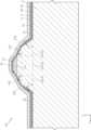
Fig. 18 is an enlarged cross-sectional view of a main portion of a thermal printhead according to a second embodiment of the present disclosure, and corresponds to Fig. 6. A thermal printhead A2 of this embodiment differs from the above-described embodiment in that each of a pair of
本実施形態に係る一対の傾斜部14はそれぞれ、図18に示すように、第1傾斜面142および第2傾斜面143を有する。第1傾斜面142と第2傾斜面143とは、y方向に並んでいる。第1傾斜面142および第2傾斜面143は、互いに主面11に対する傾斜角が異なる。第1傾斜面142は、主面11に対する傾斜角α1がたとえば54.7度である。一方、第2傾斜面143は、主面11に対する傾斜角α2がたとえば30.1度である。第1傾斜面142は、主面11と第2傾斜面143とに繋がり、これらに挟まれている。第2傾斜面143は、第1傾斜面142と頂面131(頂部13)とに繋がり、これらに挟まれている。第1傾斜面142は、(111)面である。As shown in FIG. 18, each of the pair of
サーマルプリントヘッドA2における凸部12は、たとえばサーマルプリントヘッドA1の製造方法における凸部形成工程(図8参照)後において、さらに、もう一度アルカリ水溶液によるエッチングを施すことで形成される。当該アルカリ水溶液は、KOHあるいはTMAHが用いられる。具体的には、図8に示すように凸部12を形成した後、図19に示すように、頂面131の一部にマスク層139を形成する。そして、アルカリ水溶液による異方性エッチングを施す。図19に示す例では、マスク層139は、頂面131のy方向中央付近に配置されている。これにより、図19で点描を付した部分の基材10が除去され、各々が第1傾斜面142および第2傾斜面143を有する一対の傾斜部14が形成される。本実施形態では、図8に示す1回目の異方性エッチングを施す工程と、上記した2回目の異方性エッチングを施す工程とをあわせた工程が、本開示の「エッチング工程」に相当する。その他の工程は、サーマルプリントヘッドA1の製造方法と同様である。The
本実施形態においても、第1実施形態と同様に、基材10と抵抗体層4との間に蓄熱層15が形成され、各発熱部41が発する熱が蓄熱層15に蓄えられる。また、蓄熱層15は、ガラス材料からなるグレーズであり、当該グレーズは、孔版印刷によってガラスペーストを配置して焼成することで形成される。したがって、本実施形態においても、第1実施形態と同様の効果を奏することができる。In this embodiment, as in the first embodiment, a
さらに、本実施形態によると、凸部12において、一対の傾斜部14はそれぞれ、2段階に傾斜している。つまり、各傾斜部14は、主面11に対する傾斜角が異なる第1傾斜面142および第2傾斜面143を有している。主面11に対する第2傾斜面143の傾斜角α2は、主面11に対する第1傾斜面142の傾斜角α1よりも小さい。このため、サーマルプリントヘッドA2の凸部12は、頂面131に繋がる傾斜面の傾斜角を、サーマルプリントヘッドA1の凸部12よりも小さくできる。この傾斜面は、サーマルプリントヘッドA2においては、第2傾斜面143であり、サーマルプリントヘッドA1においては、傾斜面141である。この構成によると、プラテンローラ99によって印刷媒体が搬送されたとき、凸部12への当たりを抑制できる。これにより、紙カスなどの付着防止、保護層2の摩耗防止、および、印字品質の向上などに寄与する。Furthermore, according to this embodiment, in the
第2実施形態においては、蓄熱層15が頂部13の上に形成された場合を示したが、これに限定されない。蓄熱層15は、たとえば、傾斜部14の一対の第2傾斜面143の一方あるいは両方の上にも形成されていてもよい。図20は、このような変形例に係るサーマルプリントヘッドの一例を示す要部拡大断面図であり、たとえば蓄熱層15が頂部13の上からy方向下流側の第2傾斜面143の上に跨って形成された場合を示している。本変形例によると、各発熱部41による発熱中心をy方向下流側にずらして、ストレートパスに対応させることも可能である。In the second embodiment, the
<第3実施形態>
図21は、本開示の第3実施形態に係るサーマルプリントヘッドを示す要部拡大断面図であり、図6に対応する図である。本実施形態のサーマルプリントヘッドA3は、基材10が凸部12を備えていない点で、上述した実施形態と異なっている。Third Embodiment
Fig. 21 is an enlarged cross-sectional view of a main portion of a thermal printhead according to a third embodiment of the present disclosure, and corresponds to Fig. 6. A thermal printhead A3 of this embodiment differs from the above-described embodiments in that the
図21に示すように、本実施形態に係る基材10は凸部12を備えておらず、蓄熱層15は基材10の主面11に形成されている。As shown in FIG. 21, the
サーマルプリントヘッドA3は、たとえばサーマルプリントヘッドA1の製造方法における凸部形成工程(図8参照)を省略して、準備した基材10Aを基材10として、蓄熱層形成工程を行うことで製造される。なお、蓄熱層形成工程で用いられる孔版91(93)は、スペーサ92(94)を必要としない。その後の工程は、サーマルプリントヘッドA1の製造方法と同様である。Thermal printhead A3 is manufactured by, for example, omitting the convex portion forming process (see FIG. 8) in the manufacturing method of thermal printhead A1, and instead using the
本実施形態においても、第1実施形態と同様に、基材10と抵抗体層4との間に蓄熱層15が形成され、各発熱部41が発する熱が蓄熱層15に蓄えられる。また、蓄熱層15は、ガラス材料からなるグレーズであり、当該グレーズは、孔版印刷によってガラスペーストを配置して焼成することで形成される。したがって、本実施形態においても、第1実施形態と同様の効果を奏することができる。In this embodiment, as in the first embodiment, a
さらに、本実施形態によると、基材10は凸部12を備えていない。したがって、凸部形成工程を必要とせず、製造工程を簡略化できる。Furthermore, in this embodiment, the
<第4実施形態>
図22は、本開示の第4実施形態に係るサーマルプリントヘッドを示す要部拡大断面図であり、図6に対応する図である。本実施形態のサーマルプリントヘッドA4は、蓄熱層15が絶縁層19と抵抗体層4との間に形成されていている点で、上述した実施形態と異なっている。Fourth Embodiment
Fig. 22 is an enlarged cross-sectional view of a main part of a thermal printhead according to a fourth embodiment of the present disclosure, and corresponds to Fig. 6. A thermal printhead A4 of this embodiment differs from the above-described embodiments in that a
図22に示すように、本実施形態に係る蓄熱層15は、第1~3実施形態のように、基材10と絶縁層19との間に形成されるのではなく、絶縁層19と抵抗体層4との間に形成されている。つまり、サーマルプリントヘッドA4は、基材10上に、絶縁層19、蓄熱層15、抵抗体層4の順で積層されている。As shown in FIG. 22, the
サーマルプリントヘッドA4は、たとえばサーマルプリントヘッドA1の製造方法における凸部形成工程(図8参照)の後、蓄熱層形成工程を行う前に、絶縁層19を形成することで製造される。なお、本実施形態では、絶縁層19は、基材10を熱酸化させることで得られるSiO2膜で構成されてもよい。その他の工程は、サーマルプリントヘッドA1の製造方法と同様である。 The thermal printhead A4 is manufactured, for example, by forming an insulating
本実施形態においても、第1実施形態と同様に、基材10と抵抗体層4との間に蓄熱層15が形成され、各発熱部41が発する熱が蓄熱層15に蓄えられる。また、蓄熱層15は、ガラス材料からなるグレーズであり、当該グレーズは、孔版印刷によってガラスペーストを配置して焼成することで形成される。したがって、本実施形態においても、第1実施形態と同様の効果を奏することができる。In this embodiment, as in the first embodiment, a
さらに、本実施形態によると、絶縁層19は、基材10を熱酸化させることで得られるSiO2膜で構成できる。したがって、蓄熱層15を形成した後に、たとえばCVDを用
いて材料としてTEOSを用いた成膜によりSiO2を堆積させることにより絶縁層19を形成する場合と比較して、製造工程を簡略化できる。 Furthermore, according to this embodiment, the insulating
<第5実施形態>
図23~図27は、本開示の第5実施形態に係るサーマルプリントヘッドの製造方法を示している。本実施形態においては、まず、図23に示すように、第1印刷工程を行う。この第1印刷工程は、たとえばディスペンサーを用いてガラスペースト150Aを凸部12の頂面131上に塗布する。ガラスペースト150Aは、本開示の「第1ガラスペースト」に相当する。ガラスペースト150Aの幅S1は、頂面131の寸法W2よりも小さい。なお、第1印刷工程は、ディスペンサーを用いた方法に限定されず、たとえば図9を参照して説明した孔版印刷を用いて行ってもよい。ガラスペースト150Aの材質等は特に限定されず、たとえば上述のガラスペースト15Bと同様の材質を用いればよい。Fifth Embodiment
23 to 27 show a method for manufacturing a thermal printhead according to a fifth embodiment of the present disclosure. In this embodiment, first, as shown in FIG. 23, a first printing step is performed. In this first printing step, for example, a dispenser is used to apply
次に、第1乾燥工程を行う。この第1乾燥工程では、第1印刷工程によって印刷されたガラスペースト150Aを、乾燥させる。これにより、ガラスペースト150Aが、図24に示すように乾燥ガラスペースト155Aとなる。乾燥ガラスペースト155Aは、本開示の「第1ガラスペースト」の一態様である。乾燥ガラスペースト155Aは、乾燥により、ガラスペースト150Aよりも硬い性状となっており、その形状をより維持しやすいものとなっている。Next, a first drying process is performed. In this first drying process, the
次に、第2印刷工程を行う。この第2印刷工程は、図25に示すように、乾燥ガラスペースト155A上に、たとえばディスペンサーを用いてガラスペースト150Bを塗布する。ガラスペースト150Bは、本開示の「第2ガラスペースト」に相当する。ガラスペースト150Bの幅S2は、ガラスペースト150Aの幅S1よりも小さい。なお、第2印刷工程は、ディスペンサーを用いた方法に限定されず、たとえば図9を参照して説明した孔版印刷を用いて行ってもよい。ガラスペースト150Bの材質等は特に限定されず、たとえば上述のガラスペースト15Bと同様の材質を用いればよい。Next, the second printing step is performed. In this second printing step, as shown in FIG. 25,
次に、第2乾燥工程を行う。この第2乾燥工程では、第2印刷工程によって印刷されたガラスペースト150Bを、乾燥させる。これにより、ガラスペースト150Bが、図26に示すように乾燥ガラスペースト155Bとなる。乾燥ガラスペースト155Bは、本開示の「第2ガラスペースト」の一態様である。乾燥ガラスペースト155Bは、乾燥により、ガラスペースト150Bよりも硬い性状となっており、その形状をより維持しやすいものとなっている。Next, a second drying process is performed. In this second drying process, the
次に、焼成工程を行う。この焼成工程では、乾燥ガラスペースト155Aおよび乾燥ガラスペースト155Bを焼成する。これにより、図27に示す蓄熱層15が得られる。なお、焼成工程においては、乾燥ガラスペースト155Aと乾燥ガラスペースト155Bとの双方が軟化し、互いに一体化する挙動を示す。このため、本実施形態の蓄熱層15には、乾燥ガラスペースト155Aと乾燥ガラスペースト155Bとの境界面は、判別できない状態となっている。Next, a firing process is performed. In this firing process, the dried
焼成工程において、乾燥ガラスペースト155Aおよび乾燥ガラスペースト155Bを焼成することによって、蓄熱層15を形成する。ガラスペーストの種類によっては、蓄熱層15が形成される過程において、乾燥ガラスペースト155Aおよび乾燥ガラスペースト155Bが収縮する場合がある。これにより、図27に示す凸部12の頂面131の両縁からわずかに内側に後退して、蓄熱層15が形成される。頂面131の両縁から内側に後退する長さを、後退距離dとする。後退距離dは、たとえば0μmを超えて30μm以下であり、0μmを超えて15μm以下であることが好ましい。以上の内容は、他の実施形態においても適用される。In the firing process, the
この後は、第1実施形態において説明した発熱部形成工程を含む諸工程を経ることにより、サーマルプリントヘッドが得られる。After this, the thermal printhead is obtained by going through various processes including the heating portion formation process described in the first embodiment.
本実施形態の製造方法によって得られるサーマルプリントヘッドの蓄熱層15は、寸法W2に対する寸法H2の比を、0.1~0.25とすることが可能である。発明者によって形成された寸法W2と寸法H2を例示すると、実施例1では、寸法W2が400μm、寸法H2が60μm(比率:0.15)、実施例2では、寸法W2が300μm、寸法H2が65μm(比率:0.217)、実施例3では、寸法W2が400μm、寸法H2が90μm(比率:0.225)であった。ただし、本実施形態の製造方法によって得られるサーマルプリントヘッドの蓄熱層15の上述の比は、これに限定されるものではない。The
本実施形態によっても、十分な厚みの蓄熱層15を簡易に形成することができる。特に、第1乾燥工程によってガラスペースト150Aよりも硬い性状となった乾燥ガラスペースト155A上に、第2印刷工程においてガラスペースト150Bを塗布する。これにより、ガラスペースト150Bを塗布しても、乾燥ガラスペースト155Aが扁平な形状に薄くなってしまうことを抑制することが可能である。したがって、蓄熱層15の寸法H2をより大きくすることができる。This embodiment also makes it possible to easily form a
また、乾燥ガラスペースト155Aは、いまだ焼成されていないため、焼成工程において乾燥ガラスペースト155Aと乾燥ガラスペースト155Bとが軟化し、互いに一体的なガラス体となって蓄熱層15を構成する。これは、より均質な蓄熱層15を形成するのに好ましい。In addition, since the dried
なお、上述の例においては、第2乾燥工程を行った後に、焼成工程を行った。これと異なり、たとえば図25に示すように、第2印刷工程によって乾燥ガラスペースト155A上にガラスペースト150Bを塗布した後に、第2乾燥工程を経ること無く焼成工程を行ってもよい。この場合、焼成工程においてガラスペースト150Bが不当に垂れてしまうことを抑制することが好ましく、たとえばガラスペースト150Bとして、塗布された形状をより維持しやすい材質を用いる等の方策を適宜講じてもよい。In the above example, the firing step was performed after the second drying step. Alternatively, as shown in FIG. 25, for example,
本開示に係るサーマルプリントヘッドおよびサーマルプリントヘッドの製造方法は、上述した実施形態に限定されるものではない。本開示に係るサーマルプリントヘッドの各部の具体的な構成、および、本開示に係るサーマルプリントヘッドの製造方法の各工程の具体的な処理は、種々に設計変更自在である。The thermal printhead and the method for manufacturing a thermal printhead according to the present disclosure are not limited to the above-described embodiment. The specific configuration of each part of the thermal printhead according to the present disclosure and the specific processing of each step of the method for manufacturing a thermal printhead according to the present disclosure can be freely designed in various ways.
たとえば、図3および図17などに示された複数の発熱部41に代えて、スクリーン印刷とレーザー加工とによって複数の発熱部41を形成してもよい。この場合には、まず、導電膜3Aを形成する。次に、導電膜3Aに選択的なエッチングを施すことにより、配線パターンを形成する。次に、配線パターン対してスクリーン印刷によって抵抗体ペーストを塗布することにより、抵抗体ペースト層を形成する。厚さ方向に沿って視て、抵抗体ペースト層が、複数の個別電極31の下流側のy方向先端と、複数の個別電極31に対して所定間隔を隔てて対向する各櫛歯部324のy方向上流側の先端とを含み、かつ、上述した所定間隔を含むようにして、抵抗体ペースト層を形成する。次に、抵抗体ペースト層を乾燥して焼成することによって固化し、抵抗体層4を形成。次に、焼成された抵抗体層4のうち、隣接する各櫛歯部324の間隙と隣接する各個別電極31の間隙とにy方向に沿って挟まれる部分を、レーザー加工によって除去する。除去された部分は、図3において、隣接する2個の発熱部41に挟まれた白い部分に相当する。ここまでの工程によって、図3に示された配線パターンと、複数の発熱部41とが得られる。レーザー加工に代えて、薄い円板状のダイシングブレード(回転刃)を使用して抵抗体層4を部分的に切削することによって、抵抗体層4を部分的に除去してもよい。For example, instead of the
〔付記1〕
厚さ方向の一方を向く主面を有し、単結晶半導体からなる基材と、
前記主面の上に形成され且つ主走査方向に配列された複数の発熱部を含む抵抗体層と、
前記基材と前記抵抗体層との間に形成された絶縁層と、
前記基材と前記複数の発熱部との間に形成された蓄熱層と、
を備えており、
前記蓄熱層は、ガラス材料からなるグレーズであり、
前記蓄熱層の副走査方向の寸法に対する前記厚さ方向の寸法の比率は、0.05以上0.2以下である、
サーマルプリントヘッド。
〔付記2〕
前記基材は、前記主面から突出し、かつ、前記主走査方向に延びる凸部をさらに有し、
前記蓄熱層は、前記凸部の頂部に形成されている、
付記1に記載のサーマルプリントヘッド。
〔付記3〕
前記頂部は、前記主面と平行な頂面を有する、
付記2に記載のサーマルプリントヘッド。
〔付記4〕
前記蓄熱層は、前記頂部の前記副走査方向の全幅にわたって形成されている、
付記2または3に記載のサーマルプリントヘッド。
〔付記5〕
前記凸部は、前記頂部と前記主面とに繋がり、かつ、前記主面に対して傾斜した傾斜部を有する、
付記2ないし4のいずれかに記載のサーマルプリントヘッド。
〔付記6〕
前記傾斜部は、互いに繋がる第1傾斜面および第2傾斜面を有し、
前記第1傾斜面は、前記主面に繋がり、かつ、前記主面と前記第2傾斜面とに挟まれており、
前記第2傾斜面は、前記頂部に繋がり、かつ、前記第1傾斜面と前記頂部とに挟まれており、
前記主面に対する前記第2傾斜面の傾斜角は、前記主面に対する前記第1傾斜面の傾斜角よりも小さい、
付記5に記載のサーマルプリントヘッド。
〔付記7〕
前記蓄熱層は、当該蓄熱層の上面において、前記副走査方向の両端が盛り上がるように湾曲している、
付記1ないし6のいずれかに記載のサーマルプリントヘッド。
〔付記8〕
前記抵抗体層を介して相互間を通電可能な上流側導電層および下流側導電層をさらに備えており、
前記抵抗体層は、前記主面および前記蓄熱層に跨って形成され、
前記上流側導電層および前記下流側導電層は、前記抵抗体層の一部を露出させて前記抵抗体層上に積層されており、
前記複数の発熱部はそれぞれ、前記抵抗体層のうち前記上流側導電層および前記下流側導電層から露出する部分である、
付記1ないし7のいずれかに記載のサーマルプリントヘッド。
〔付記9〕
前記絶縁層は、前記蓄熱層を覆っている、
付記1ないし8のいずれかに記載のサーマルプリントヘッド。
〔付記10〕
前記単結晶半導体は、Siからなり、
前記主面は、(100)面である、
付記1ないし9のいずれかに記載のサーマルプリントヘッド。
〔付記11〕
前記蓄熱層の前記厚さ方向の寸法は、30μm以上200μm以下である、
付記1ないし10のいずれかに記載のサーマルプリントヘッド。
〔付記12〕
前記蓄熱層の前記厚さ方向の寸法は、50μm以上60μm以下である、
付記11に記載のサーマルプリントヘッド。
〔付記13〕
単結晶半導体からなる基材を準備する準備工程と、
前記基材の上に、第1ガラスペーストを配置する第1印刷工程と、
前記第1ガラスペーストを焼成することで、第1グレーズを形成する第1グレーズ形成工程と、
前記第1グレーズの上に、主走査方向に配列された複数の発熱部を形成する発熱部形成工程と、
を備えている、
サーマルプリントヘッドの製造方法。
〔付記14〕
前記第1グレーズ形成工程で形成された前記第1グレーズの上に、第2ガラスペーストを配置する第2印刷工程と、
前記第2ガラスペーストを焼成することで、前記第1グレーズよりも厚さが厚い第2グレーズを形成する第2グレーズ形成工程と、
をさらに備えている、
付記13に記載のサーマルプリントヘッドの製造方法。
〔付記15〕
前記第1印刷工程および前記第2印刷工程のうち少なくともいずれか一方では、金属板にスリットが形成された孔版を用いて印刷を行う、
付記14に記載のサーマルプリントヘッドの製造方法。
〔付記16〕
前記第2印刷工程で用いられる孔版のスリットの副走査方向の寸法は、前記第1印刷工程で用いられる孔版のスリットの前記副走査方向の寸法の8割以上9割以下である、
付記15に記載のサーマルプリントヘッドの製造方法。
〔付記17〕
前記第1印刷工程および前記第2印刷工程のうち少なくともいずれか一方では、メッシュを有するスクリーンマスクを用いて印刷を行う、
付記14に記載のサーマルプリントヘッドの製造方法。
〔付記18〕
前記第1印刷工程より前に行われ、前記基材に異方性エッチングを施すエッチング工程をさらに備え、
前記エッチング工程では、異方性エッチングにより、前記基材に、厚さ方向の一方を向く主面と、当該主面から突出した凸部とを形成し、
前記第1グレーズ形成工程では、前記凸部の頂部に前記第1グレーズを形成する、
付記13ないし17のいずれかに記載のサーマルプリントヘッドの製造方法。
〔付記19〕
前記第1グレーズ形成工程と前記発熱部形成工程との間に行われ、前記第1グレーズおよび前記基材を覆う絶縁層を形成する絶縁層形成工程をさらに備えている、
付記13ないし18のいずれかに記載のサーマルプリントヘッドの製造方法。
〔付記20〕
単結晶半導体からなる基材を準備する準備工程と、
前記基材の上に、第1ガラスペーストを配置する第1印刷工程と、
前記第1ガラスペーストを乾燥する第1乾燥工程と、
乾燥後の前記第1ガラスペースト上に第2ガラスペーストを配置する第2印刷工程と、
前記第1ガラスペーストおよび前記第2ガラスペーストを焼成することで、蓄熱層を形成する焼成工程と、
前記蓄熱層の上に、主走査方向に配列された複数の発熱部を形成する発熱部形成工程と、
を備えている、
サーマルプリントヘッドの製造方法。
〔付記21〕
前記第2印刷工程の後、前記焼成工程の前に、前記第2ガラスペーストを乾燥する第2乾燥工程をさらに備える、
付記20に記載のサーマルプリントヘッドの製造方法。
〔付記22〕
厚さ方向の一方を向く主面を有し、単結晶半導体からなる基材と、
前記主面の上に形成され且つ主走査方向に配列された複数の発熱部を含む抵抗体層と、
前記基材と前記抵抗体層との間に形成された絶縁層と、
前記基材と前記複数の発熱部との間に形成された蓄熱層と、
を備えており、
前記蓄熱層は、ガラス材料からなるグレーズであり、
前記蓄熱層の副走査方向の寸法に対する前記厚さ方向の寸法の比率は、0.10以上0.25以下である、
サーマルプリントヘッド。[Appendix 1]
a substrate having a main surface facing in one direction of a thickness and made of a single crystal semiconductor;
a resistor layer including a plurality of heat generating portions formed on the main surface and arranged in a main scanning direction;
an insulating layer formed between the substrate and the resistor layer;
A heat storage layer formed between the base material and the plurality of heat generating portions;
Equipped with
The heat storage layer is a glaze made of a glass material,
a ratio of the thickness direction dimension of the heat storage layer to the sub-scanning direction dimension is 0.05 or more and 0.2 or less;
Thermal print head.
[Appendix 2]
the base material further has a protrusion protruding from the main surface and extending in the main scanning direction,
The heat storage layer is formed on the top of the protrusion.
2. The thermal printhead of
[Appendix 3]
The top portion has a top surface parallel to the main surface.
3. The thermal printhead of
[Appendix 4]
The heat storage layer is formed over the entire width of the top portion in the sub-scanning direction.
4. The thermal printhead according to
[Appendix 5]
the protrusion has an inclined portion that is connected to the top and the main surface and is inclined with respect to the main surface;
5. A thermal printhead according to any one of
[Appendix 6]
the inclined portion has a first inclined surface and a second inclined surface that are connected to each other,
the first inclined surface is connected to the main surface and is sandwiched between the main surface and the second inclined surface,
the second inclined surface is connected to the apex and is sandwiched between the first inclined surface and the apex,
an inclination angle of the second inclined surface with respect to the main surface is smaller than an inclination angle of the first inclined surface with respect to the main surface;
6. The thermal printhead of
[Appendix 7]
The heat storage layer is curved such that both ends in the sub-scanning direction rise on the upper surface of the heat storage layer.
7. A thermal printhead according to any one of
[Appendix 8]
The resistor layer may further include an upstream conductive layer and a downstream conductive layer that are capable of conducting electricity between each other through the resistor layer,
the resistor layer is formed across the main surface and the heat storage layer,
the upstream conductive layer and the downstream conductive layer are laminated on the resistor layer with a portion of the resistor layer exposed,
each of the plurality of heat generating portions is a portion of the resistor layer that is exposed from the upstream conductive layer and the downstream conductive layer;
8. A thermal printhead according to any one of
[Appendix 9]
The insulating layer covers the heat storage layer.
9. A thermal printhead according to any one of
[Appendix 10]
the single crystal semiconductor is made of Si,
The main surface is a (100) surface.
10. A thermal printhead according to any one of
[Appendix 11]
The dimension of the heat storage layer in the thickness direction is 30 μm or more and 200 μm or less.
11. A thermal printhead according to any one of
[Appendix 12]
The dimension of the heat storage layer in the thickness direction is 50 μm or more and 60 μm or less.
12. The thermal printhead of
[Appendix 13]
A preparation step of preparing a substrate made of a single crystal semiconductor;
a first printing step of disposing a first glass paste on the substrate;
a first glaze forming step of forming a first glaze by firing the first glass paste;
a heat generating portion forming step of forming a plurality of heat generating portions arranged in a main scanning direction on the first glaze;
Equipped with
A method for manufacturing a thermal printhead.
[Appendix 14]
a second printing step of disposing a second glass paste on the first glaze formed in the first glaze forming step;
A second glaze forming step of forming a second glaze having a thickness greater than that of the first glaze by firing the second glass paste;
Further comprising:
14. A method for manufacturing the thermal printhead according to
[Appendix 15]
In at least one of the first printing step and the second printing step, printing is performed using a stencil having slits formed in a metal plate.
15. A method for manufacturing a thermal printhead according to
[Appendix 16]
The dimension of the slit in the sub-scanning direction of the stencil used in the second printing step is 80% or more and 90% or less of the dimension of the slit in the sub-scanning direction of the stencil used in the first printing step.
A method for manufacturing a thermal printhead according to
[Appendix 17]
In at least one of the first printing step and the second printing step, printing is performed using a screen mask having a mesh.
15. A method for manufacturing a thermal printhead according to
[Appendix 18]
The method further includes an etching step, which is performed before the first printing step, and which performs anisotropic etching on the base material;
In the etching step, a main surface facing one side in a thickness direction and a convex portion protruding from the main surface are formed in the base material by anisotropic etching;
In the first glaze forming step, the first glaze is formed on the top of the convex portion.
A method for manufacturing a thermal printhead according to any one of
[Appendix 19]
The method further includes an insulating layer forming step, which is performed between the first glaze forming step and the heat generating portion forming step, and forms an insulating layer that covers the first glaze and the base material.
A method for manufacturing a thermal printhead according to any one of
[Appendix 20]
A preparation step of preparing a substrate made of a single crystal semiconductor;
a first printing step of disposing a first glass paste on the substrate;
a first drying step of drying the first glass paste;
a second printing step of disposing a second glass paste on the first glass paste after drying;
a firing step of firing the first glass paste and the second glass paste to form a heat storage layer;
a heat generating portion forming step of forming a plurality of heat generating portions arranged in a main scanning direction on the heat storage layer;
Equipped with
A method for manufacturing a thermal printhead.
[Appendix 21]
The method further includes a second drying step of drying the second glass paste after the second printing step and before the firing step.
21. A method for manufacturing a thermal printhead according to claim 20.
[Appendix 22]
a substrate having a main surface facing in one direction of a thickness and made of a single crystal semiconductor;
a resistor layer including a plurality of heat generating portions formed on the main surface and arranged in a main scanning direction;
an insulating layer formed between the substrate and the resistor layer;
A heat storage layer formed between the base material and the plurality of heat generating portions;
Equipped with
The heat storage layer is a glaze made of a glass material,
a ratio of the thickness direction dimension of the heat storage layer to the sub-scanning direction dimension is 0.10 or more and 0.25 or less;
Thermal print head.
A1~A4:サーマルプリントヘッド
1 :ヘッド基板
10 :基材
11 :主面
12 :凸部
13 :頂部
131 :頂面
14 :傾斜部
141 :傾斜面
142 :第1傾斜面
143 :第2傾斜面
15 :蓄熱層
151 :ラウンド部
19 :絶縁層
2 :保護層
21 :パッド用開口
3 :電極層
31 :個別電極
311 :電極パッド部
32 :共通電極
323 :共通部
324 :櫛歯部
4 :抵抗体層
41 :発熱部
5 :接続基板
59 :コネクタ
61 :ワイヤ
62 :ワイヤ
7 :ドライバIC
78 :保護樹脂
8 :放熱部材
99 :プラテンローラ
10A :基材
11A :主面
15A :グレーズ
15B :ガラスペースト
15C :グレーズ
150A,150B:ガラスペースト
155A,155B:乾燥ガラスペースト
3A :導電膜
4A :抵抗体膜
91,93:孔版
91a,93a:スリット
92 :スペーサ
139 :マスク層A1 to A4: Thermal print head 1: Head substrate 10: Base material 11: Main surface 12: Convex portion 13: Top portion 131: Top surface 14: Inclined portion 141: Inclined surface 142: First inclined surface 143: Second inclined surface 15: Heat storage layer 151: Rounded portion 19: Insulating layer 2: Protective layer 21: Pad opening 3: Electrode layer 31: Individual electrode 311: Electrode pad portion 32: Common electrode 323: Common portion 324: Comb-tooth portion 4: Resistor layer 41: Heat generating portion 5: Connection substrate 59: Connector 61: Wire 62: Wire 7: Driver IC
78: Protective resin 8: Heat dissipation member 99:
Claims (20)
Translated fromJapanese前記主面の上に形成され且つ主走査方向に配列された複数の発熱部を含む抵抗体層と、
前記基材と前記抵抗体層との間に形成された絶縁層と、
前記基材と前記複数の発熱部との間に形成された蓄熱層と、
を備えており、
前記蓄熱層は、ガラス材料からなるグレーズであり、
前記蓄熱層の副走査方向の寸法に対する前記厚さ方向の寸法の比率は、0.05以上0.2以下であり、
前記基材は、前記主面から突出し、かつ、前記主走査方向に延びる凸部をさらに有し、
前記蓄熱層は、前記凸部の頂部に形成されており、
前記蓄熱層は、前記頂部の前記副走査方向の全幅にわたって形成されている、
サーマルプリントヘッド。 a substrate having a main surface facing in one direction of a thickness and made of a single crystal semiconductor;
a resistor layer including a plurality of heat generating portions formed on the main surface and arranged in a main scanning direction;
an insulating layer formed between the substrate and the resistor layer;
A heat storage layer formed between the base material and the plurality of heat generating portions;
Equipped with
The heat storage layer is a glaze made of a glass material,
a ratio of a dimension of the heat storage layer in the thickness direction to a dimension in the sub-scanning directionis 0.05 or more and 0.2 or less;
the base material further has a protrusion protruding from the main surface and extending in the main scanning direction,
The heat storage layer is formed on the top of the protrusion,
The heat storage layer is formed over the entire width of the top portion in the sub-scanning direction.
Thermal print head.
請求項1に記載のサーマルプリントヘッド。 The top portion has a top surface parallel to the main surface.
2. The thermal printhead of claim1 .
請求項1または2に記載のサーマルプリントヘッド。 the protrusion has an inclined portion that is connected to the top and the main surface and is inclined with respect to the main surface;
3. The thermal printhead according to claim1 or 2 .
前記第1傾斜面は、前記主面に繋がり、かつ、前記主面と前記第2傾斜面とに挟まれており、
前記第2傾斜面は、前記頂部に繋がり、かつ、前記第1傾斜面と前記頂部とに挟まれており、
前記主面に対する前記第2傾斜面の傾斜角は、前記主面に対する前記第1傾斜面の傾斜角よりも小さい、
請求項3に記載のサーマルプリントヘッド。 the inclined portion has a first inclined surface and a second inclined surface that are connected to each other,
the first inclined surface is connected to the main surface and is sandwiched between the main surface and the second inclined surface,
the second inclined surface is connected to the apex and is sandwiched between the first inclined surface and the apex,
an inclination angle of the second inclined surface with respect to the main surface is smaller than an inclination angle of the first inclined surface with respect to the main surface;
4. The thermal printhead according to claim3 .
請求項1ないし4のいずれかに記載のサーマルプリントヘッド。 The heat storage layer is curved such that both ends in the sub-scanning direction rise on the upper surface of the heat storage layer.
5. A thermal printhead according to claim 1.
前記主面の上に形成され且つ主走査方向に配列された複数の発熱部を含む抵抗体層と、a resistor layer including a plurality of heat generating portions formed on the main surface and arranged in a main scanning direction;
前記基材と前記抵抗体層との間に形成された絶縁層と、an insulating layer formed between the substrate and the resistor layer;
前記基材と前記複数の発熱部との間に形成された蓄熱層と、A heat storage layer formed between the base material and the plurality of heat generating portions;
を備えており、Equipped with
前記蓄熱層は、ガラス材料からなるグレーズであり、The heat storage layer is a glaze made of a glass material,
前記蓄熱層の副走査方向の寸法に対する前記厚さ方向の寸法の比率は、0.05以上0.2以下であり、a ratio of a dimension of the heat storage layer in the thickness direction to a dimension in the sub-scanning direction is 0.05 or more and 0.2 or less;
前記蓄熱層は、当該蓄熱層の上面において、前記副走査方向の両端が盛り上がるように湾曲している、The heat storage layer is curved such that both ends in the sub-scanning direction rise on the upper surface of the heat storage layer.
サーマルプリントヘッド。Thermal print head.
前記抵抗体層は、前記主面および前記蓄熱層に跨って形成され、
前記上流側導電層および前記下流側導電層は、前記抵抗体層の一部を露出させて前記抵抗体層上に積層されており、
前記複数の発熱部はそれぞれ、前記抵抗体層のうち前記上流側導電層および前記下流側導電層から露出する部分である、
請求項1ないし6のいずれかに記載のサーマルプリントヘッド。 The resistor layer may further include an upstream conductive layer and a downstream conductive layer that are capable of conducting electricity between each other through the resistor layer,
the resistor layer is formed across the main surface and the heat storage layer,
the upstream conductive layer and the downstream conductive layer are laminated on the resistor layer with a portion of the resistor layer exposed,
each of the plurality of heat generating portions is a portion of the resistor layer that is exposed from the upstream conductive layer and the downstream conductive layer;
7. A thermal printhead according to claim 1.
請求項1ないし7のいずれかに記載のサーマルプリントヘッド。 The insulating layer covers the heat storage layer.
8. A thermal printhead according to claim 1.
前記主面は、(100)面である、
請求項1ないし8のいずれかに記載のサーマルプリントヘッド。 the single crystal semiconductor is made of Si,
The main surface is a (100) surface.
9. A thermal printhead according to claim 1.
請求項1ないし9のいずれかに記載のサーマルプリントヘッド。 The dimension of the heat storage layer in the thickness direction is 30 μm or more and 200 μm or less.
10. A thermal printhead according to claim 1.
前記主面の上に形成され且つ主走査方向に配列された複数の発熱部を含む抵抗体層と、a resistor layer including a plurality of heat generating portions formed on the main surface and arranged in a main scanning direction;
前記基材と前記抵抗体層との間に形成された絶縁層と、an insulating layer formed between the substrate and the resistor layer;
前記基材と前記複数の発熱部との間に形成された蓄熱層と、A heat storage layer formed between the base material and the plurality of heat generating portions;
を備えており、Equipped with
前記蓄熱層は、ガラス材料からなるグレーズであり、The heat storage layer is a glaze made of a glass material,
前記蓄熱層の副走査方向の寸法に対する前記厚さ方向の寸法の比率は、0.05以上0.2以下であり、a ratio of a dimension of the heat storage layer in the thickness direction to a dimension in the sub-scanning direction is 0.05 or more and 0.2 or less;
前記蓄熱層の前記厚さ方向の寸法は、30μm以上200μm以下である、The dimension of the heat storage layer in the thickness direction is 30 μm or more and 200 μm or less.
サーマルプリントヘッド。Thermal print head.
請求項10または11に記載のサーマルプリントヘッド。 The dimension of the heat storage layer in the thickness direction is 50 μm or more and 60 μm or less.
12. The thermal printhead according to claim10 or 11.
前記基材の上に、第1ガラスペーストを配置する第1印刷工程と、
前記第1ガラスペーストを焼成することで、第1グレーズを形成する第1グレーズ形成工程と、
前記第1グレーズの上に、主走査方向に配列された複数の発熱部を形成する発熱部形成工程と、
を備えており、
前記第1グレーズ形成工程で形成された前記第1グレーズの上に、第2ガラスペーストを配置する第2印刷工程と、
前記第2ガラスペーストを焼成することで、前記第1グレーズよりも厚さが厚い第2グレーズを形成する第2グレーズ形成工程と、
をさらに備えている、
サーマルプリントヘッドの製造方法。 A preparation step of preparing a substrate made of a single crystal semiconductor;
a first printing step of disposing a first glass paste on the substrate;
a first glaze forming step of forming a first glaze by firing the first glass paste;
a heat generating portion forming step of forming a plurality of heat generating portions arranged in a main scanning direction on the first glaze;
Equippedwith
a second printing step of disposing a second glass paste on the first glaze formed in the first glaze forming step;
A second glaze forming step of forming a second glaze having a thickness greater than that of the first glaze by firing the second glass paste;
Further comprising:
A method for manufacturing a thermal printhead.
請求項13に記載のサーマルプリントヘッドの製造方法。 In at least one of the first printing step and the second printing step, printing is performed using a stencil having slits formed in a metal plate.
The method for manufacturing the thermal printhead according to claim13 .
請求項14に記載のサーマルプリントヘッドの製造方法。 The dimension of the slit in the sub-scanning direction of the stencil used in the second printing step is 80% or more and 90% or less of the dimension of the slit in the sub-scanning direction of the stencil used in the first printing step.
The method for manufacturing the thermal printhead according to claim14 .
請求項13に記載のサーマルプリントヘッドの製造方法。 In at least one of the first printing step and the second printing step, printing is performed using a screen mask having a mesh.
The method for manufacturing the thermal printhead according to claim13 .
前記エッチング工程では、異方性エッチングにより、前記基材に、厚さ方向の一方を向く主面と、当該主面から突出した凸部とを形成し、
前記第1グレーズ形成工程では、前記凸部の頂部に前記第1グレーズを形成する、
請求項13ないし16のいずれかに記載のサーマルプリントヘッドの製造方法。 The method further includes an etching step, which is performed before the first printing step, and which performs anisotropic etching on the base material;
In the etching step, a main surface facing one side in a thickness direction and a convex portion protruding from the main surface are formed in the base material by anisotropic etching;
In the first glaze forming step, the first glaze is formed on the top of the convex portion.
A method for manufacturing a thermal printhead according to any one of claims 13 to16 .
請求項13ないし17のいずれかに記載のサーマルプリントヘッドの製造方法。 The method further includes an insulating layer forming step, which is performed between the first glaze forming step and the heat generating portion forming step, and forms an insulating layer that covers the first glaze and the base material.
A method for manufacturing a thermal printhead according to any one of claims 13 to17 .
前記基材の上に、第1ガラスペーストを配置する第1印刷工程と、
前記第1ガラスペーストを乾燥する第1乾燥工程と、
乾燥後の前記第1ガラスペースト上に第2ガラスペーストを配置する第2印刷工程と、
前記第1ガラスペーストおよび前記第2ガラスペーストを焼成することで、蓄熱層を形成する焼成工程と、
前記蓄熱層の上に、主走査方向に配列された複数の発熱部を形成する発熱部形成工程と、
を備えている、
サーマルプリントヘッドの製造方法。 A preparation step of preparing a substrate made of a single crystal semiconductor;
a first printing step of disposing a first glass paste on the substrate;
a first drying step of drying the first glass paste;
a second printing step of disposing a second glass paste on the first glass paste after drying;
a firing step of firing the first glass paste and the second glass paste to form a heat storage layer;
a heat generating portion forming step of forming a plurality of heat generating portions arranged in a main scanning direction on the heat storage layer;
Equipped with
A method for manufacturing a thermal printhead.
請求項19に記載のサーマルプリントヘッドの製造方法。 The method further includes a second drying step of drying the second glass paste after the second printing step and before the firing step.
The method for manufacturing the thermal printhead according to claim19 .
Applications Claiming Priority (2)
| Application Number | Priority Date | Filing Date | Title |
|---|---|---|---|
| JP2020009878 | 2020-01-24 | ||
| JP2020009878 | 2020-01-24 |
Publications (2)
| Publication Number | Publication Date |
|---|---|
| JP2021115854A JP2021115854A (en) | 2021-08-10 |
| JP7545858B2true JP7545858B2 (en) | 2024-09-05 |
Family
ID=77173754
Family Applications (1)
| Application Number | Title | Priority Date | Filing Date |
|---|---|---|---|
| JP2020171779AActiveJP7545858B2 (en) | 2020-01-24 | 2020-10-12 | Thermal printhead and method for manufacturing the same |
Country Status (1)
| Country | Link |
|---|---|
| JP (1) | JP7545858B2 (en) |
Families Citing this family (2)
| Publication number | Priority date | Publication date | Assignee | Title |
|---|---|---|---|---|
| JP2023082289A (en)* | 2021-12-02 | 2023-06-14 | ローム株式会社 | THERMAL PRINT HEAD AND METHOD FOR MANUFACTURING THERMAL PRINT HEAD |
| JPWO2023223776A1 (en)* | 2022-05-16 | 2023-11-23 |
Citations (3)
| Publication number | Priority date | Publication date | Assignee | Title |
|---|---|---|---|---|
| JP2002103660A (en) | 2000-09-29 | 2002-04-09 | Kyocera Corp | Thermal head |
| US20110074907A1 (en) | 2009-09-30 | 2011-03-31 | Toshimitsu Morooka | Thermal head, printer, and manufacturing method for thermal head |
| JP2019014233A (en) | 2017-06-08 | 2019-01-31 | ローム株式会社 | Thermal print head |
Family Cites Families (2)
| Publication number | Priority date | Publication date | Assignee | Title |
|---|---|---|---|---|
| JPH04288244A (en)* | 1991-03-18 | 1992-10-13 | Alps Electric Co Ltd | Thermal head |
| JP3124873B2 (en)* | 1993-09-10 | 2001-01-15 | アルプス電気株式会社 | Thermal head and method of manufacturing the same |
- 2020
- 2020-10-12JPJP2020171779Apatent/JP7545858B2/enactiveActive
Patent Citations (3)
| Publication number | Priority date | Publication date | Assignee | Title |
|---|---|---|---|---|
| JP2002103660A (en) | 2000-09-29 | 2002-04-09 | Kyocera Corp | Thermal head |
| US20110074907A1 (en) | 2009-09-30 | 2011-03-31 | Toshimitsu Morooka | Thermal head, printer, and manufacturing method for thermal head |
| JP2019014233A (en) | 2017-06-08 | 2019-01-31 | ローム株式会社 | Thermal print head |
Also Published As
| Publication number | Publication date |
|---|---|
| JP2021115854A (en) | 2021-08-10 |
Similar Documents
| Publication | Publication Date | Title |
|---|---|---|
| JP7545858B2 (en) | Thermal printhead and method for manufacturing the same | |
| JP7413066B2 (en) | Thermal print head manufacturing method, thermal print head and thermal printer | |
| JP7481158B2 (en) | Thermal printheads and thermal printers | |
| JP7037941B2 (en) | Thermal print head | |
| JP7269802B2 (en) | Thermal print head and manufacturing method thereof | |
| JP7151054B2 (en) | Thermal print head and manufacturing method thereof | |
| WO2021149617A1 (en) | Thermal print head and method for manufacturing thermal print head | |
| JP7630494B2 (en) | Thermal printhead and method for manufacturing the same | |
| JP7297564B2 (en) | Thermal print head and manufacturing method thereof | |
| JP6867768B2 (en) | Thermal print head | |
| JP7393218B2 (en) | Thermal print head manufacturing method and thermal print head | |
| US11400731B2 (en) | Thermal printhead | |
| JP2023082289A (en) | THERMAL PRINT HEAD AND METHOD FOR MANUFACTURING THERMAL PRINT HEAD | |
| JP7219634B2 (en) | thermal print head | |
| JP7557320B2 (en) | Thermal Printhead | |
| JP7627228B2 (en) | Thermal printhead and manufacturing method thereof | |
| CN114103477B (en) | Thermal print head, method for manufacturing thermal print head, and thermal printer | |
| JP7754689B2 (en) | Thermal printhead and method for manufacturing the same | |
| US11305553B2 (en) | Thermal print head and method of manufacturing thermal print head | |
| JP7607504B2 (en) | Thermal printhead and method for manufacturing the same | |
| JP7398244B2 (en) | Method for forming heat storage layer and method for manufacturing thermal print head | |
| JP7310069B2 (en) | thermal print head | |
| US20220097409A1 (en) | Thermal print head | |
| JP2023121941A (en) | thermal print head | |
| JP2023121322A (en) | Thermal print head, method for manufacturing thermal print head, and thermal printer |
Legal Events
| Date | Code | Title | Description |
|---|---|---|---|
| A621 | Written request for application examination | Free format text:JAPANESE INTERMEDIATE CODE: A621 Effective date:20230906 | |
| A977 | Report on retrieval | Free format text:JAPANESE INTERMEDIATE CODE: A971007 Effective date:20240419 | |
| A131 | Notification of reasons for refusal | Free format text:JAPANESE INTERMEDIATE CODE: A131 Effective date:20240507 | |
| A521 | Request for written amendment filed | Free format text:JAPANESE INTERMEDIATE CODE: A523 Effective date:20240704 | |
| TRDD | Decision of grant or rejection written | ||
| A01 | Written decision to grant a patent or to grant a registration (utility model) | Free format text:JAPANESE INTERMEDIATE CODE: A01 Effective date:20240806 | |
| A61 | First payment of annual fees (during grant procedure) | Free format text:JAPANESE INTERMEDIATE CODE: A61 Effective date:20240826 | |
| R150 | Certificate of patent or registration of utility model | Ref document number:7545858 Country of ref document:JP Free format text:JAPANESE INTERMEDIATE CODE: R150 |