JP7545094B2 - System and method for manufacturing optical integrated circuits - Google Patents
System and method for manufacturing optical integrated circuitsDownload PDFInfo
- Publication number
- JP7545094B2 JP7545094B2JP2023502000AJP2023502000AJP7545094B2JP 7545094 B2JP7545094 B2JP 7545094B2JP 2023502000 AJP2023502000 AJP 2023502000AJP 2023502000 AJP2023502000 AJP 2023502000AJP 7545094 B2JP7545094 B2JP 7545094B2
- Authority
- JP
- Japan
- Prior art keywords
- optical
- film
- refractive index
- measurement
- core
- Prior art date
- Legal status (The legal status is an assumption and is not a legal conclusion. Google has not performed a legal analysis and makes no representation as to the accuracy of the status listed.)
- Active
Links
Images


Classifications
- G—PHYSICS
- G02—OPTICS
- G02B—OPTICAL ELEMENTS, SYSTEMS OR APPARATUS
- G02B6/00—Light guides; Structural details of arrangements comprising light guides and other optical elements, e.g. couplings
- G02B6/10—Light guides; Structural details of arrangements comprising light guides and other optical elements, e.g. couplings of the optical waveguide type
- G02B6/12—Light guides; Structural details of arrangements comprising light guides and other optical elements, e.g. couplings of the optical waveguide type of the integrated circuit kind
- G02B6/13—Integrated optical circuits characterised by the manufacturing method
- G02B6/132—Integrated optical circuits characterised by the manufacturing method by deposition of thin films
Landscapes
- Physics & Mathematics (AREA)
- Engineering & Computer Science (AREA)
- Microelectronics & Electronic Packaging (AREA)
- General Physics & Mathematics (AREA)
- Optics & Photonics (AREA)
- Optical Integrated Circuits (AREA)
Description
Translated fromJapanese本発明は、光周期回路の製造工程における製造誤差および効率を改善する方法および製造システムに関する。The present invention relates to a method and manufacturing system for improving manufacturing errors and efficiency in the manufacturing process of optical periodic circuits.
半導体レーザ、フォトダイオード、光波長合分波器、光スイッチなどは光ファイバ通信のキーとなる光デバイスである。半導体レーザは、光の発振器として、情報信号を重畳するためのキャリアとなる光波を生成する。フォトダイオードは、光信号の強度を電気信号に変換する素子として動作する。また、アレイ導波路格子に代表される光波長合分波器は、異なる光の波長を合波・分波する素子として波長分割多重通信に用いられる(例えば、非特許文献2参照)。さらに光スイッチは、光の経路をルーティングする素子としてROADM(Reconfigurable Optical Add/Drop Multiplexing)システムにおいて重要な機能を持つ。これらの光デバイスは、光集積回路として構成され得る。光ファイバ通信においては、伝送媒体である光ファイバはもちろん、光信号処理を行うこれら光デバイスの光集積回路が重要な役割を果たす(例えば、非特許文献1参照)。Semiconductor lasers, photodiodes, optical wavelength multiplexers/demultiplexers, optical switches, etc. are key optical devices in optical fiber communications. Semiconductor lasers, as optical oscillators, generate light waves that serve as carriers for superimposing information signals. Photodiodes operate as elements that convert the intensity of optical signals into electrical signals. Optical wavelength multiplexers/demultiplexers, as typified by arrayed waveguide gratings, are used in wavelength division multiplexing communications as elements that multiplex and demultiplex different wavelengths of light (see, for example, Non-Patent Document 2). Furthermore, optical switches have an important function in ROADM (Reconfigurable Optical Add/Drop Multiplexing) systems as elements that route optical paths. These optical devices can be configured as optical integrated circuits. In optical fiber communications, not only optical fiber, which is the transmission medium, but also optical integrated circuits of these optical devices that process optical signals play an important role (see, for example, Non-Patent Document 1).
光集積回路は、一般に基板上に形成された光導波路により構成される。光導波路は、光信号が伝搬するコアとそれを取り囲むクラッドからなる。半導体レーザやフォトダイオードは、InPなどの半導体材料により構成され、アレイ導波路格子や光スイッチは、主に石英ガラスからなる光導波路材料により構成される。Optical integrated circuits are generally composed of optical waveguides formed on a substrate. An optical waveguide consists of a core through which optical signals propagate and a cladding that surrounds it. Semiconductor lasers and photodiodes are made of semiconductor materials such as InP, while arrayed waveguide gratings and optical switches are made of optical waveguide materials that are mainly made of quartz glass.
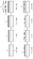
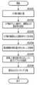
図1は、従来技術の光導波路の製造方法を示す図である。ここでは、石英系ガラスからなる石英系平面光波回路を例に典型的な製造工程を説明する。最初に、1:下部クラッド堆積工程において、シリコン基板(ウェハ)11上に下部クラッド12となるガラス膜を堆積する。下部クラッド12は、火炎堆積法(FHD:Flame Hydrolysis Deposition)により堆積されたP2O5やB2O3を添加したSiO2からなる。FHD法で堆積されたスート状のガラス粒子を1000℃以上の高温で加熱し、透明な下部クラッド12を得る。次に2:コア堆積工程において、同じくFHD法を用いて、下部クラッド12よりも高い屈折率を有するコア13となる薄膜ガラスを堆積する。コア13の堆積にあたっては、GeO2をSiO2に添加することにより、所望の屈折率値を得ることができる。1:下部クラッド堆積工程と同様に1000℃以上の高温で加熱し、透明なコア13を形成する。 FIG. 1 is a diagram showing a conventional method for manufacturing an optical waveguide. Here, a typical manufacturing process will be described using a silica-based planar lightwave circuit made of silica-based glass as an example. First, in the 1: lower clad deposition process, a glass film that will become the
3:フォトレジスト成膜工程において、スピンコートにより基板上にフォトレジスト膜14を成膜する。次に、4:回路パターン露光工程において、フォトマスク15を介してUV光16をフォトレジスト膜に照射することにより、マスクパターンに応じた回路パターンを露光する。そして、5:フォトレジスト現像工程において、フォトレジスト膜の回路パターンを現像し、フォトレジストパターン17を得る。In step 3: photoresist deposition process, a
次に、6:エッチング工程において、反応性イオンエッチング(RIE:Reactive Ion Etching)により、フォトレジストパターン17をコアに転写し、コアパターン18を得る。さらに、7:レジスト除去工程において、コア上に残ったフォトレジストをアッシングにより除去する。最後に、8:上部クラッド堆積工程において、上述の1:下部クラッド堆積工程における下部クラッド堆積と同様の方法によって、上部クラッド19を堆積する。Next, in step 6: etching, the
上述の製造工程によって得られる光導波路に対して、光回路のパターンサイズや光学特性など種々の検査が行われる。従来、これらの検査結果を製造工程に反映するにあたっては、上述の図1の一連の工程が全て終了した後、それぞれの工程に対して、検査結果を反映した製造条件を設定していた。検査結果のこのような反映方法では、それぞれの工程における製造誤差が累積していく。この累積誤差のため、図1に示した工程の後工程になるほど、各工程で得られる検査結果の精度が低くなり、検査結果の反映が不正確になる問題があった。一工程が終了した時点で得られた検査結果から、現在の工程の製造条件を再設定したり、後工程の製造条件を調整したりすることにより、製造誤差の累積を抑えることもできる。しかしながらこのような反映方法では、一工程ごとに製造工程を中断することになり、製造工程のスループットを向上させることが難しいという問題もあった。Various inspections such as the pattern size and optical characteristics of the optical circuit are performed on the optical waveguide obtained by the above-mentioned manufacturing process. Conventionally, when reflecting these inspection results in the manufacturing process, after all of the series of processes in FIG. 1 are completed, manufacturing conditions that reflect the inspection results are set for each process. In this method of reflecting the inspection results, manufacturing errors in each process accumulate. Due to this accumulated error, the accuracy of the inspection results obtained in each process decreases the later the process shown in FIG. 1, and there was a problem that the reflection of the inspection results becomes inaccurate. It is also possible to suppress the accumulation of manufacturing errors by resetting the manufacturing conditions of the current process or adjusting the manufacturing conditions of the later process based on the inspection results obtained at the time of the completion of one process. However, with this reflection method, the manufacturing process is interrupted after each process, and there was also a problem that it was difficult to improve the throughput of the manufacturing process.
とりわけ図1の製造工程における2:コア堆積工程で形成されるコア膜は、光導波路のコアの光学特性に大きな影響を与える。このため、コア膜の堆積工程およびコアの加工工程は、製造工程の全体の品質やコストを決定する重要な位置を占めている。In particular, the core film formed in step 2: Core Deposition Process in the manufacturing process of Figure 1 has a significant impact on the optical properties of the core of the optical waveguide. For this reason, the core film deposition process and the core processing process occupy important positions in determining the overall quality and cost of the manufacturing process.
コア膜の堆積工程において生じる誤差の影響を抑え、製造工程へ精度良く、効率的に反映させる光集積回路の製造システム、製造方法が求められている。There is a demand for a manufacturing system and method for optical integrated circuits that can reduce the impact of errors that occur during the core film deposition process and accurately and efficiently reflect these in the manufacturing process.
本発明の1つの実施態様は、ウェハの面内において、コア膜の膜厚分布および屈折率分布を取得するステップと、前記膜厚分布および前記屈折率分布に基づいて、光導波路の構造値の補正量分布を決定するステップと、前記ウェハの中の1つ以上の露光単位領域に対して、前記補正量分布に対応したマスクを選択するステップと、前記選択されたマスクを使用して、前記ウェハの上のフォトレジスト膜を露光するステップとを備えることを特徴とする光集積回路の製造方法である。One embodiment of the present invention is a method for manufacturing an optical integrated circuit, comprising the steps of acquiring a film thickness distribution and a refractive index distribution of a core film within the plane of a wafer, determining a correction amount distribution of a structural value of an optical waveguide based on the film thickness distribution and the refractive index distribution, selecting a mask corresponding to the correction amount distribution for one or more exposure unit areas in the wafer, and exposing a photoresist film on the wafer using the selected mask.
本発明のもう1つの実施態様は、光集積回路の製造システムであって、ウェハの面内において、コア膜の膜厚分布および屈折率分布を取得する測定部と、前記膜厚分布および前記屈折率分布に基づいて、光導波路の構造値の補正量分布を決定する算出部と、前記ウェハの中の1つ以上の露光単位領域に対して、前記補正量分布に対応したマスクを選択し、前記選択されたマスクを使用して、前記ウェハの上のフォトレジスト膜を露光する露光部とを備えたことを特徴とする。Another embodiment of the present invention is a manufacturing system for optical integrated circuits, characterized in that it comprises a measurement unit that acquires a thickness distribution and a refractive index distribution of a core film within the surface of a wafer, a calculation unit that determines a correction amount distribution of a structural value of an optical waveguide based on the thickness distribution and the refractive index distribution, and an exposure unit that selects a mask corresponding to the correction amount distribution for one or more exposure unit areas in the wafer, and exposes a photoresist film on the wafer using the selected mask.
光集積回路の製造工程の品質およびスループットを向上することができる。The quality and throughput of the manufacturing process for optical integrated circuits can be improved.
発明者らは、従来技術の光回路の製造工程における検査結果の反映について、検査結果から得られる情報データの利用方法を新しい視点から見直した。図1に示した従来技術の一連の製造方法では、最終段階の検査結果を得た後で、検査結果に基づいた情報を先行する前の工程にフィードバックしていた。その結果として、最終段階で取得される光特性などの検査結果の値は、各工程における累積的な誤差を含んだものであった。またフィードバックによる工程改善の点でも、直接関係の無い工程へも含めて、累積的な誤差を含んだ情報に基づいて工程条件の変更・調整が成されていた。フィードバック量やその精度、フィードバックの行き先やタイミングの点で十分に効果的なものとは言えなかった。The inventors have taken a fresh look at how information data obtained from inspection results is used in the manufacturing process of optical circuits using conventional technology. In the series of manufacturing methods of the conventional technology shown in Figure 1, after the inspection results of the final stage are obtained, information based on the inspection results is fed back to the preceding process. As a result, the inspection result values of optical characteristics and the like obtained in the final stage contain cumulative errors in each process. In terms of process improvement through feedback, too, changes and adjustments to process conditions are made based on information containing cumulative errors, even for processes that are not directly related. This cannot be said to be sufficiently effective in terms of the amount of feedback, its accuracy, and the destination and timing of the feedback.
しかしながら、ある工程で得られる加工結果の情報、例えばフォトリソグラフィ現像工程で得られるレジストパターン幅の情報を、その現像工程の直後に知ることができれば、後工程であるエッチング工程においてパターン幅の情報を反映することができる。また、コア堆積工程で得られるコアの膜厚や屈折率を、その堆積工程の直後に知ることができれば、後のフォトリソグラフィ工程やエッチング工程で形成される光導波路の光学特性を予測することもできる。このように、先行する前工程で得られる光導波路構成要素の特性値を、その前工程中または直後に取得することにより、引き続く後工程の加工条件に反映し、その後工程で得られる光学特性の予測および改善に用いることができる。However, if information on the processing results obtained in a certain process, for example information on the resist pattern width obtained in a photolithography development process, could be known immediately after that development process, the pattern width information could be reflected in the subsequent etching process. Also, if the film thickness and refractive index of the core obtained in the core deposition process could be known immediately after that deposition process, the optical characteristics of the optical waveguide formed in the subsequent photolithography and etching processes could be predicted. In this way, by obtaining the characteristic values of the optical waveguide components obtained in the preceding pre-process during or immediately after that pre-process, they can be reflected in the processing conditions of the subsequent post-process and used to predict and improve the optical characteristics obtained in the subsequent process.
本開示の一連の発明では、複数の製造工程で得られる工程情報、工程データは、それらの情報、データが得られているその工程中、さらに引き続く次の工程へ「フィードフォワード」される。このようなフィードフォワードによる製造工程の改善は、製造工程のスループットの点でも好都合である。In the series of inventions disclosed herein, process information and process data obtained in multiple manufacturing processes are "feed forward" to the process in which the information and data are obtained, and to the next subsequent process. Improvements to the manufacturing process through such feed forward are also advantageous in terms of throughput of the manufacturing process.
以下の実施形態は、光回路の製造工程で取得できる検査結果・データを、より効率的に精度良く工程に反映できる製造システム、製造方法、製造方法を改善する光回路の構成などについて開示する。特に本明細書では、コア膜堆積工程において取得される工程データを後工程に効果的に反映させ、コア膜堆積工程の誤差を軽減する製造システムおよび製造方法に焦点を合わせて説明する。最初に、図面を参照しながら、本開示の光回路の製造方法の基本的概念から説明を始める。The following embodiments disclose a manufacturing system and manufacturing method that can more efficiently and accurately reflect the inspection results and data obtained in the manufacturing process of an optical circuit in the process, and an optical circuit configuration that improves the manufacturing method. In particular, this specification focuses on a manufacturing system and manufacturing method that effectively reflects process data obtained in the core film deposition process in subsequent processes and reduces errors in the core film deposition process. First, the basic concept of the manufacturing method for the optical circuit disclosed herein will be explained with reference to the drawings.
[実施形態1]
本実施形態の光回路の製造方法では、製造工程における一工程を実施中に形成され、取得される、光デバイスの構成要素または特性についてのデータに着目する。このデータは、リアルデータまたは現在のデータと言うこともできる。光デバイスの構成要素または特性について計測を行い、その計測して得られたデータに基づいて、後工程の製造条件を調整しまたは補正を行う(以下この方式を「フィードフォワードシステム」とも言う)。フィードフォワードシステムにより、光デバイスの光学特性のバラツキを抑制し、最終的に得られる光デバイスについて所望の光学特性を得ることを可能にする。[Embodiment 1]
In the manufacturing method of the optical circuit of this embodiment, attention is focused on data on the components or characteristics of the optical device that is formed and acquired during one step of the manufacturing process. This data can also be called real data or current data. The components or characteristics of the optical device are measured, and the manufacturing conditions of the subsequent steps are adjusted or corrected based on the data obtained from the measurement (hereinafter, this method is also called a "feedforward system"). The feedforward system suppresses the variation in the optical characteristics of the optical device, making it possible to obtain the desired optical characteristics for the finally obtained optical device.
図2は、本開示の実施形態1に係る光導波路を含む光回路の製造方法を示す図である。フィードフォワードシステムは、一工程で形成される光デバイスの構成要素について「計測」を行い、この計測結果に基づいて光学特性推定処理21によって「光学特性推定」を行う。そして、推定結果に基づき、プロセスコントロール処理22によって後工程のプロセスの「制御」を行う。Figure 2 is a diagram showing a manufacturing method for an optical circuit including an optical waveguide according to
例えば、図2の下部クラッド堆積工程1で形成される下部クラッド膜の屈折率および厚さ、コア堆積工程2において堆積するコア層の屈折率および厚さを「計測」する。この測定結果に基づいて、標準の(ノミナルの)設計値で作製されたデバイスの最終的な光学特性を推定する。そしてこの推定に基づいて、後工程であるエッチング工程6において、エッチングの強度またはエッチング時間を「制御」する。For example, the refractive index and thickness of the lower cladding film formed in lower
具体的には、「計測」したコア層の膜厚および屈折率、クラッド膜の屈折率に基づいて、光デバイスとして要求される性能を満たすためのパターンの理想的なコア幅を推定(予測)する。そしてエッチング工程6では、この予測値に基づいてエッチングを行う。例えば、標準の(nominal)設計値では「コア加工後の導波路幅が太く」、所望の性能を満たすことができないという予測情報の場合、エッチング工程で、形成されるコア幅を細くする補正を行う。この時の調整(補正)方法としては、エッチング時間を短く/長くするまたはエッチング強度を弱く/強くすることにより、コア幅を太く/細くする方法がある。さらに、エッチング工程6で形成される導波路のパターンにおけるコアの幅や段差を「計測」することができる。この計測結果に基づき、上部クラッド堆積工程8で形成する上部クラッド膜の屈折率などを「制御」し、最終的に得られる光導波路の光学特性を調整することもできる。Specifically, based on the "measured" film thickness and refractive index of the core layer and the refractive index of the cladding film, the ideal core width of the pattern to meet the performance required for the optical device is estimated (predicted). Then, in the etching process 6, etching is performed based on this predicted value. For example, if the predicted information indicates that the "waveguide width after core processing is too wide" with the standard (nominal) design value and the desired performance cannot be met, a correction is made in the etching process to narrow the core width. The adjustment (correction) method at this time is to shorten/lengthen the etching time or weaken/strengthen the etching strength to make the core width wider/narrower. Furthermore, the core width and step in the waveguide pattern formed in the etching process 6 can be "measured". Based on the measurement results, the refractive index of the upper cladding film formed in the upper cladding deposition process 8 can be "controlled" to adjust the optical characteristics of the optical waveguide finally obtained.
上述のように本発実施形態のフィードフォワードシステムは、光デバイスを製造する複数の工程のうち、前工程の工程中またはその工程後に、形成された光デバイスの構成要素の形状、特性等を測定する。この測定結果に基づいて、後工程における製造条件を調整または補正を行う。As described above, the feedforward system of the present embodiment measures the shape, characteristics, etc. of the components of the formed optical device during or after a front-end process among the multiple processes for manufacturing the optical device. Based on the measurement results, the manufacturing conditions in the back-end process are adjusted or corrected.
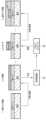
図3は、実施形態1のフィードフォワードシステムを一般化して示した図である。フィードフォワードシステムは、M個の工程からなる光デバイスの製造手順を含み、製造対象物である光デバイスを、工程1、工程2・・・、工程i、・・・工程j、・・・工程Mの順序で実施する。ここで、i<jのとき、工程jは工程iより時間的に後の工程である。フィードフォワードシステムは、計測データ処理部31および制御データ処理部32を含む。計測データ処理部31は、図2で説明した光学特性推定処理21を実行し、制御データ処理部32は、図2で説明したプロセスコントロール処理22を実行する。計測データ処理部31および制御データ処理部32は、CPU、RAM、ROMなどを有して構成されるコンピュータの形態とすることができる。Figure 3 is a diagram showing a generalized feedforward system of
図3のフィードフォワードシステムにおいて、実線は製造対象物の工程に従った流れを示している。また、破線はそれぞれの工程の「計測」によって得られる計測データを、また、一点鎖線はそれぞれの工程に対する「制御」のための制御データを、それぞれ示している。図3のように、本実施形態のフィードフォワードシステムは、工程iで、その工程の製造装置またはその計測装置から計測データを取得し、計測データ処理部31へと転送する。計測データ処理部31は、転送された計測データに基づいて、工程iで形成される光デバイスの構成要素の形状または特性を予測する。また、計測データに基づいて、最終的に得られる光デバイスの光学特性を、工程iにおいて予測することもできる。In the feedforward system of Figure 3, the solid lines indicate the flow of the manufacturing process. The dashed lines indicate the measurement data obtained by "measurement" of each process, and the dashed lines indicate the control data for "control" of each process. As shown in Figure 3, the feedforward system of this embodiment acquires measurement data from the manufacturing equipment or measurement equipment of that process in process i, and transfers it to the measurement
計測データ処理部31で導出された予測値は、制御データ処理部32に渡される。制御データ処理部32は、予測値に基づいて、後工程である工程jにおける製造条件を求める。制御データ処理部32は、工程jが実施される際に、求めた製造条件に応じて、製造装置に設定する工程j用の制御データを供給する。後工程jを実施する際に供給される、前工程に基づく制御データは、前工程iに基づく制御データのみであっても良いし、前工程のいくつかに基づく複数種類の制御データであっても良い。制御データの形態は、実際に構成される製造装置および製造対象物などの条件に応じて定められることはもちろんである。The predicted value derived by the measurement
[実施形態2]
本実施形態では、実施形態1のフィードフォワードシステムの2:コア堆積工程で生じる誤差が後工程へ与える影響を最小化する光集積回路の製造方法、製造システムについて説明する。図1の従来技術の製造工程における2:コア堆積工程から6:エッチング工程までの改善に相当する。図3のフィードフォワードシステムにおいて、コア膜を堆積する工程からの工程データ(コア膜の膜厚分布データおよび屈折率分布データ)に基づいて、回路パターン露光工程へフィードフォワードする仕組みが開示される。最初に、コア膜の堆積工程が後工程および光集積回路の光学特性に与える影響について説明し、その後、本開示の光集積回路の製造方法および製造システムについて説明する。 [Embodiment 2]
In this embodiment, a method and system for manufacturing an optical integrated circuit that minimizes the effect of errors occurring in the 2: core deposition process of the feedforward system of
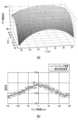
図4は、光集積回路が形成されるウェハ面内におけるコア膜特性のバラツキを示す図である。図4の(a)は、ウェハ面内の光学膜厚のプロットと、プロット点をフィッティングした光学膜厚の分布曲面を3次元的に示した図である。概ね直径120mmのウェハ面内(x-y面)において、垂直方向軸に正規化した光学膜厚(nm)をプロットしている。「光学膜厚」は、コア膜に対して光学膜厚=膜厚×屈折率の関係で表され、ウェハ面内でこの光学膜厚の分布を求めることができる。また、コア膜特性としてコア膜の膜厚および屈折率、下部および上部クラッドの屈折率の各分布を取得することできる。これらの分布は、コア膜に対して光導波路が形成された後で、光信号の伝搬特性を表す指標である等価屈折率neの情報を得るために重要である。等価屈折率neについては、さらに後述する。図4の(b)は、別の直径300mmのウェハのコア膜について1次元の屈折率分布を示した図である。後述する実施形態4によりフィッティングした曲線も示している。 FIG. 4 is a diagram showing the variation of core film characteristics in the wafer surface on which an optical integrated circuit is formed. FIG. 4(a) is a diagram showing a plot of optical film thickness in the wafer surface and a three-dimensional distribution curve of optical film thickness with fitting of plot points. In the wafer surface (x-y plane) with a diameter of approximately 120 mm, the optical film thickness (nm) normalized on the vertical axis is plotted. The "optical film thickness" is expressed as the relationship of optical film thickness = film thickness x refractive index with respect to the core film, and the distribution of this optical film thickness can be obtained in the wafer surface. In addition, the distributions of the film thickness and refractive index of the core film, and the refractive index of the lower and upper clads can be obtained as the core film characteristics. These distributions are important for obtaining information on the equivalent refractive index ne , which is an index representing the propagation characteristics of an optical signal after an optical waveguide is formed in the core film. The equivalent refractive index ne will be described further below. FIG. 4(b) is a diagram showing the one-dimensional refractive index distribution of the core film of another wafer with a diameter of 300 mm. A curve fitted by the fourth embodiment described later is also shown.
図4の(a)では、ウェハ面内で光学膜厚が分布している状態が良く確認できる。図4の(b)の例でも、コア膜の屈折率はウェハ中央部から周辺に向かって小さくなるように分布している。コア膜の膜厚、下部および上部クラッドの屈折率についても同様に、面内の分布形状を取得することができる(詳細は実施形態3、4)。ウェハ面内におけるコア膜の膜厚および屈折率、下部および上部クラッドの屈折率の各バラツキは、ウェハ全面に作製される光集積回路の複数のチップ間で、光学特性のバラツキにつながる。これらの膜特性が変化することで光が感じる位相に影響する等価屈折率neが変化し、同一の回路パターンを使用していても後述する光の位相進み量がウェハ内でばらつくことになる。また1つのチップ内に多数の光干渉回路を備えたような光集積回路では、1つのチップ内でも光干渉回路毎に光学特性にバラツキが生じることになる。コア膜の光の光学特性のバラツキを示す光学膜厚に加えて、もう1つの指標は光導波路の等価屈折率neである。 In FIG. 4(a), the distribution of the optical film thickness within the wafer surface can be clearly seen. In the example of FIG. 4(b), the refractive index of the core film is also distributed so as to decrease from the center of the wafer toward the periphery. The distribution shape within the surface can be obtained for the thickness of the core film and the refractive index of the lower and upper clads (see the third and fourth embodiments for details). The variations in the thickness and refractive index of the core film within the wafer surface and the refractive index of the lower and upper clads lead to variations in the optical characteristics among multiple chips of the optical integrated circuit fabricated on the entire wafer. The equivalent refractive index ne that affects the phase sensed by the light changes due to the change in these film characteristics, and the phase advance of the light, which will be described later, varies within the wafer even if the same circuit pattern is used. In addition, in an optical integrated circuit having many optical interferometers within one chip, the optical characteristics will vary for each optical interferometer even within one chip. In addition to the optical film thickness that indicates the variation in the optical characteristics of the core film, another index is the equivalent refractive index ne of the optical waveguide.
最初に述べたように、キーとなる光デバイスを集積化した光集積回路は、その重要な構成要素として光導波路を含んでいる。光デバイスは光導波路デバイスと言うこともできる。したがって、光導波路の構造や光学特性の製造誤差を抑えることが重要である。また光集積回路の重要で大規模なものの多くには、マッハツェンダー干渉計(MZI:Mach-Zehnder Interferometer)やアレイ導波路回折格子(AWG:Arrayed Waveguide Grating)が含まれている。MZIやAWGの機能は、光が通過する1つ以上の光導波路の経路に起因して生じる光の位相差を利用した干渉現象に基づいている。光導波路を伝搬する光信号の位相は、光導波路の伝搬特性によって直接的に影響を受け、この伝搬特性は、等価屈折率neによって決定される。 As mentioned at the beginning, optical integrated circuits that integrate key optical devices include optical waveguides as their important components. Optical devices can also be called optical waveguide devices. Therefore, it is important to suppress manufacturing errors in the structure and optical characteristics of optical waveguides. Many important and large-scale optical integrated circuits also include Mach-Zehnder Interferometers (MZIs) and arrayed waveguide gratings (AWGs). The function of MZIs and AWGs is based on the interference phenomenon that utilizes the phase difference of light caused by the path of one or more optical waveguides through which light passes. The phase of an optical signal propagating through an optical waveguide is directly affected by the propagation characteristics of the optical waveguide, and this propagation characteristic is determined by the equivalent refractive index ne .
図5は、光導波路における等価屈折率の算出を説明するための図である。図5には、以下説明する等価屈折率を求める光導波路の断面構成を示している。波長λの光信号が、長さLおよび等価屈折率neの光導波路を伝搬するとき、光信号の位相の進み量φは次式で表される。
図5に示したように光導波路の断面形状が矩形の場合、光導波路の等価屈折率neは、光導波路コアの幅aおよび高さbと、コア屈折率ncore、クラッド屈折率ncladから決定される。例えば非特許文献3および非特許文献4では、矩形コアについて、その形状、コア屈折率、クラッド屈折率から、x成分、y成分の各電場の分散方程式を用いて、伝搬定数βおよび等価屈折率neを求める手順が開示されている。以下、等価屈折率neの計算の概略を示す。図5の断面構成の光導波路コアに対して、第1象限のみを考慮してx軸方向およびy軸方向についてそれぞれ分散方程式を解く。 When the cross-sectional shape of the optical waveguide is rectangular as shown in Fig. 5, the equivalent refractive index ne of the optical waveguide is determined from the width a and height b of the optical waveguide core, the core refractive index ncore , and the cladding refractive index nclad . For example, Non-Patent Documents 3 and 4 disclose a procedure for determining the propagation constant β and the equivalent refractive index ne for a rectangular core using the dispersion equations of the electric fields of the x and y components from the shape, core refractive index, and cladding refractive index. The calculation of the equivalent refractive index ne is outlined below. For the optical waveguide core with the cross-sectional configuration of Fig. 5, the dispersion equations are solved for the x-axis direction and the y-axis direction, respectively, taking into account only the first quadrant.
x軸方向については、次式が得られる。

同様にy軸方向について、次式が得られる。

上式において、pはx軸の横方向電磁界成分の山の数、qはy軸の横方向電磁界成分の山の数である。上の式(2)~(9)から伝搬定数βを求め、さらに等価屈折率neが次のように求められる。

上式から、光導波路の等価屈折率neが、コアの幅aおよび高さbと、コア屈折率ncore、クラッド屈折率ncladから決定されることがわかる。From the above formula, it can be seen that the equivalent refractive index ne of the optical waveguide is determined by the width a and height b of the core, the core refractive index ncore , and the cladding refractive index nclad .
MZIやAWGのような光回路の光学特性は、光導波路の伝搬特性を表す等価屈折率neによって強く影響される。したがって、光集積回路の製造工程では等価屈折率neを決定する光導波路コアの幅、高さおよびコアの屈折率を安定して制御する必要がある。一方で図4の(a)、(b)に示したように、コア膜の堆積工程を終了した段階で、コア膜の膜厚、屈折率は均一ではなく分布を持っており、光回路の光学特性のバラツキに直結することが理解できるだろう。光導波路コアの高さとなるコア膜の厚さ、コア膜の屈折率の変動は、いずれも光学膜厚および等価屈折率neの各指標に直接影響するのは明らかである。 The optical characteristics of optical circuits such as MZI and AWG are strongly influenced by the equivalent refractive index ne , which represents the propagation characteristics of the optical waveguide. Therefore, in the manufacturing process of optical integrated circuits, it is necessary to stably control the width and height of the optical waveguide core and the refractive index of the core, which determine the equivalent refractive index ne . On the other hand, as shown in (a) and (b) of FIG. 4, at the stage where the deposition process of the core film is completed, the film thickness and refractive index of the core film are not uniform but have a distribution, which can be understood as being directly linked to the variation in the optical characteristics of the optical circuit. It is clear that the thickness of the core film, which is the height of the optical waveguide core, and the fluctuation in the refractive index of the core film both directly affect the respective indicators of the optical film thickness and the equivalent refractive index ne .
発明者らは、コア膜の堆積工程を終了した段階で得られるコア膜の情報を、引き続く光導波路形成のいずれかの後工程に反映させ、コア膜堆積工程で生じた誤差の影響を抑えることができないか検討した。上述の光の伝搬状態を表す指標の内、コア膜の光学膜厚(=屈折率×コア膜厚)、屈折率、膜厚は、コア膜の堆積工程が終了した段階でウェハの面内分布として測定できる。また下部クラッドの屈折率分布についても、同様に測定することができる。目標光学特性から決定されるこれらの設定値と、実測値との差分は、それぞれの目標値からの逸脱量、すなわち製造誤差に対応している。引き続く光導波路の作製工程において、変更可能な光導波路の構造値に対して、この逸脱量を相殺するような補正ができるのではないかと考えた。The inventors have considered whether it is possible to suppress the influence of errors that occur in the core film deposition process by reflecting the core film information obtained at the end of the core film deposition process in any of the subsequent processes of the optical waveguide formation. Among the indices that indicate the above-mentioned light propagation state, the optical film thickness (= refractive index x core film thickness), refractive index, and film thickness of the core film can be measured as the in-plane distribution of the wafer at the end of the core film deposition process. The refractive index distribution of the lower cladding can also be measured in the same way. The difference between these set values determined from the target optical characteristics and the actual measured values corresponds to the deviation from each target value, that is, the manufacturing error. It was thought that it would be possible to make a correction to offset this deviation in the structural values of the optical waveguide that can be changed in the subsequent optical waveguide fabrication process.
コア膜の堆積工程の後の、光導波路の作製工程において、現実的に変更可能な構造値としては、後に詳述するように、ウェハ上に構成される少なくとも一部の光回路のコア幅、コアの厚さ、光導波路の物理的長さなどがある。コア膜の堆積より後工程の光導波路の作製工程において適用できるこれらの構造値への補正量を決定することで、コア膜の堆積工程で生じたコア膜のウェハ面内の誤差分布を抑えることができるはずである。このように光導波路の作製工程で変更可能な構造値に補正を加えることは、光導波路が作製された状態の等価屈折率neの補正を行っているのと実質的に同じである。 In the process of fabricating the optical waveguide after the deposition of the core film, the structural values that can be changed in practice include the core width, the core thickness, and the physical length of the optical waveguide of at least a part of the optical circuit formed on the wafer, as described in detail later. By determining the amount of correction to these structural values that can be applied in the process of fabricating the optical waveguide after the deposition of the core film, it should be possible to suppress the error distribution in the wafer surface of the core film that occurs in the deposition of the core film. Applying correction to the structural values that can be changed in the fabrication process of the optical waveguide in this way is substantially the same as correcting the equivalent refractive index ne in the state in which the optical waveguide is fabricated.
既に説明した通り、コア膜がエッチングされてコア幅が決まりコアの形状が確定しない限り、最終的な等価屈折率neを求めることはできない。しかしながら、光導波路の作製の前であっても、光学膜厚やコア膜の厚さおよび屈折率の実測データに対して、例えばコア幅の値を一定値と仮定すれば、簡易的に、一定の精度で等価屈折率neを推定することもできる。光導波路の作製工程の前段階でも、その後の工程を実施する場合に推定される等価屈折率neに基づき、その等価屈折率neに補正が加えられるように、後工程の製造条件を修正できる。例えば、推定される等価屈折率neが設定値よりも大きくなるのであれば、等価屈折率neが小さくなるように光導波路の構造値を補正できる。逆に推定される等価屈折率neが設定値よりも小さくなるのであれば、等価屈折率neが大きくなるように光導波路の構造値を補正すれば良い。このように図3のフィードフォワードの考え方をコア膜堆積工程に適用し、コア膜堆積工程より後工程の製造条件・工程の修正することによって、光集積回路の光学特性のバラツキを抑え、歩留を上げてコストダウンを実現できる。 As already explained, the final equivalent refractive index ne cannot be obtained unless the core film is etched, the core width is determined, and the core shape is confirmed. However, even before the optical waveguide is manufactured, if the core width is assumed to be a constant value for the actual measurement data of the optical film thickness, the core film thickness, and the refractive index, the equivalent refractive index ne can be estimated simply and with a certain degree of accuracy. Even before the optical waveguide is manufactured, the manufacturing conditions of the subsequent process can be corrected so that the equivalent refractive index ne is corrected based on the equivalent refractive index ne estimated when the subsequent process is performed. For example, if the estimated equivalent refractive index ne is larger than the set value, the structural value of the optical waveguide can be corrected so that the equivalent refractive index ne is smaller. Conversely, if the estimated equivalent refractive index ne is smaller than the set value, the structural value of the optical waveguide can be corrected so that the equivalent refractive index ne is larger. In this way, by applying the feedforward concept of FIG. 3 to the core film deposition process and correcting the manufacturing conditions and processes of the processes subsequent to the core film deposition process, the variation in the optical characteristics of the optical integrated circuit can be suppressed, the yield can be increased, and costs can be reduced.
本実施形態の光集積回路の製造方法では、コア膜の堆積工程で得られるコア膜のウェハ面内工程データを利用して、引き続く光導波路の作製工程における光導波路の構造値を補正する。コア膜のウェハ面内の工程データには、コア膜の膜厚分布データ、コア膜の屈折率分布データを含む。本実施形態では、光導波路コアを作製するための露光・エッチング工程の前で、ウェハ面(x-y面)に平行な方向における光導波路の構造値に対して、補正量分布を決定する。その後、決定された光導波路の構造値の補正量分布にしたがって、ウェハ内の光集積回路の露光単位領域毎に対応するマスクを選択する。以下、図面を参照しながら、本実施形態の光集積回路の製造方法の詳細を説明する。In the manufacturing method of the optical integrated circuit of this embodiment, the process data within the wafer surface of the core film obtained in the deposition process of the core film is used to correct the structural values of the optical waveguide in the subsequent manufacturing process of the optical waveguide. The process data within the wafer surface of the core film includes the film thickness distribution data of the core film and the refractive index distribution data of the core film. In this embodiment, before the exposure and etching process for manufacturing the optical waveguide core, a correction amount distribution is determined for the structural values of the optical waveguide in a direction parallel to the wafer surface (x-y surface). Then, according to the determined correction amount distribution of the structural values of the optical waveguide, a mask corresponding to each exposure unit area of the optical integrated circuit in the wafer is selected. The manufacturing method of the optical integrated circuit of this embodiment will be described in detail below with reference to the drawings.
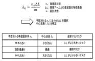
図6は、コア膜の堆積工程データに基づいて、光導波路の構造値を補正する方法の概念を説明する図である。図6の左側から右側に向かって光回路の製造工程が進行し、図2では製造方法の2:コア堆積工程から6:エッチング工程に対応する。図6の上側に従来技術の製造工程におけるコア膜堆積工程の誤差の発生とその結果に至るまでの関係が示されており、下側の本実施形態の製造方法と対比している。図6には様々な「値」が矢印で示されており、矢印の上下方向の位置がその値の大小関係を示している。以後の説明では、各値を次のように定義する。Figure 6 is a diagram explaining the concept of a method for correcting the structural values of an optical waveguide based on core film deposition process data. The manufacturing process of the optical circuit progresses from left to right in Figure 6, and in Figure 2 corresponds to 2: core deposition process to 6: etching process of the manufacturing method. The upper part of Figure 6 shows the occurrence of errors in the core film deposition process in the manufacturing process of the conventional technology and the relationship leading to the result, and is compared with the manufacturing method of this embodiment in the lower part. Various "values" are indicated by arrows in Figure 6, and the vertical position of the arrow indicates the magnitude relationship of the values. In the following explanation, each value is defined as follows:
「光学特性値」は、光回路の機能や性能を表す指標値であって、例えばMZIの中心波長やAWGの透過帯域の中心波長であり得る。図6には示していないが、コア膜「目標値」は、決定された目標光学特性値1010(仕様)に対して、特定の光導波路を構成するのに必要なコア膜の構造や特性の目標値(Target value)である。したがって、コア膜「目標値」は光学特性の設計仕様が同一である限り、不変である。例えば、コア膜の膜厚目標値や屈折率目標値であり得る。The "optical characteristic value" is an index value that represents the function or performance of an optical circuit, and can be, for example, the central wavelength of an MZI or the central wavelength of an AWG transmission band. Although not shown in FIG. 6, the "target value" of the core film is the target value of the structure and characteristics of the core film required to configure a specific optical waveguide for the determined target optical characteristic value 1010 (specification). Therefore, the "target value" of the core film remains unchanged as long as the design specifications for the optical characteristics remain the same. For example, it can be the target thickness value or refractive index value of the core film.
図6に示した「コア膜設定値」1011は、光導波路を実際の製造工程で作製するために、実際のコア堆積工程に対して設定される値である。初期状態の製造工程では、コア膜設定値1011は、コア膜目標値となる。コア膜実測値1012は、コア堆積工程の終了後に、実測されたコア膜の膜厚およびコア膜の屈折率のウェハ面内分布データを含む。図4で説明したように、ウェハ面内のコア膜特性は分布しばらついているので、図6のコア膜実測値1012はコア膜設定値1011に対してずれ、逸脱が生じる。図6では、一例としてウェハ面内のある位置においてコア膜実測値1012がコア膜設定値1011よりも小さい方向(下方)にずれたものとする。具体的には、コア膜厚の実測値がコア膜厚の設定値よりも小さくなった状態を想定されたい。本実施形態の製造方法に好適な、コア膜の屈折率の測定方法は、実施形態3として後述する。The "core film set value" 1011 shown in FIG. 6 is a value set for the actual core deposition process in order to fabricate the optical waveguide in the actual manufacturing process. In the initial manufacturing process, the core
上述のコア膜実測値の逸脱は、従来技術の製造方法および本発明の製造方法のいずれについても、同様に生じる。図6の上側に示した従来技術では、コア膜堆積工程で生じた誤差がそのまま光導波路作製のための露光・エッチング工程まで維持され、工程終了時に得られる結果光学特性値1013も目標光学特性値1010から逸脱したものであった。従来技術では、工程終了後にコア膜設定値1011に対してフィードバックをしていたため、その精度やスループットなど既に述べた問題を生じていた。The deviation of the actual core film value described above occurs in the same way in both the conventional manufacturing method and the manufacturing method of the present invention. In the conventional technology shown in the upper part of Figure 6, the error that occurred in the core film deposition process was maintained until the exposure and etching process for fabricating the optical waveguide, and the resultant optical
一方、図6の下側に示した本実施形態の製造方法では、コア膜堆積工程の後の露光・エッチング工程における光導波路の構造値に対して「補正」が実施される。具体的には、光導波路コアの構造値に対して「補正量」が決定される。光導波路の構造値に対して補正して露光・エッチング工程を実施することによって、コア膜堆積工程で生じたコア膜実測値1012で検出された誤差、逸脱が相殺される。工程終了後には、コア膜堆積工程でコア膜設定値1011に対する誤差が生じていないのと実質的に等価な状態へ近づけることができる。光導波路の構造値の決定された補正量を露光・エッチング工程に適用することは、実質的に等価屈折率neを補正していることになる。このように本開示の製造方法では、ウェハ面内におけるコア膜の膜厚や屈折率の実測値分布に基づき、予め光導波路の構造値の補正量を決定し、この補正量に基づいた工程変更を露光・エッチング工程に適用することで、最終工程の結果光学特性値1016の誤差が最小化される。 On the other hand, in the manufacturing method of the present embodiment shown in the lower part of FIG. 6, a "correction" is performed on the structural value of the optical waveguide in the exposure/etching process after the core film deposition process. Specifically, a "correction amount" is determined for the structural value of the optical waveguide core. By performing the exposure/etching process with a correction to the structural value of the optical waveguide, the error and deviation detected in the core film
本実施形態の製造方法において、コア膜の膜厚実測値分布や屈折率実測値分布に基づいて補正する光導波路の構造値は、光導波路コア幅、光干渉回路を構成する光導波路のコア長さ、光干渉回路における2つ以上の光導波路間の物理長差を含む。露光・エッチング工程における工程変更は、ウェハ上のフォトレジスト膜の露光工程において、露光単位領域毎に、光導波路の構造値の補正量分布に対応したマスクを選択することによって実施される。したがって、ウェハ面内の位置に応じて、チップ毎に異なるマスクが選択され得る。In the manufacturing method of this embodiment, the structural values of the optical waveguide that are corrected based on the distribution of measured film thickness and refractive index of the core film include the optical waveguide core width, the core length of the optical waveguide that constitutes the optical interferometer, and the physical length difference between two or more optical waveguides in the optical interferometer. Process changes in the exposure and etching process are implemented by selecting a mask that corresponds to the distribution of correction amounts for the structural values of the optical waveguide for each exposure unit area in the exposure process of the photoresist film on the wafer. Therefore, a different mask can be selected for each chip depending on the position within the wafer surface.
露光単位領域は、1つの選択されたマスクによって光回路を形成する最小領域を意味している。光集積回路の製造工程では、半導体露光装置によって、投影光学系を利用してウェハ上に任意の位置に異なる転写用回路パターンを露光することができる。露光単位領域は、1つのマスクのショット(転写)によりウェハ内に構成され、1つのチップの全領域またはチップ内の一部の領域に対応し得る。また、1つのチップ内に複数の露光単位領域が存在しても良い。例えば、1つのチップ内に同一構成の複数の光干渉回路が含まれる光集積回路では、1つの光干渉回路で構成される領域が露光単位領域となる。1つのチップ領域内で、光干渉回路毎に、異なるマスクが選択され得る。An exposure unit area means the smallest area in which an optical circuit is formed by one selected mask. In the manufacturing process of an optical integrated circuit, a semiconductor exposure apparatus can expose different transfer circuit patterns at any position on a wafer using a projection optical system. An exposure unit area is formed in a wafer by a shot (transfer) of one mask, and can correspond to the entire area of one chip or a partial area within the chip. In addition, there may be multiple exposure unit areas in one chip. For example, in an optical integrated circuit that includes multiple optical interferometers with the same configuration in one chip, the area formed by one optical interferometer becomes an exposure unit area. Within one chip area, a different mask can be selected for each optical interferometer.
図7は、実施形態2の光集積回路の製造方法を実施する製造システムの概略図である。製造システム1000におけるウェハフローは、図1および図2の製造工程フローに概ね対応している。製造システム1000は、ウェハの面内において、コア膜の膜厚分布および屈折率分布を取得する測定部1001を備える。さらに、膜厚分布および屈折率分布に基づいて、光導波路の構造値の補正量分布を決定するコア膜補正量の算出部1002と、露光・エッチング装置1003を備える。露光・エッチング装置1003は、ウェハの中の1つ以上の露光単位領域に対して、上述の補正量分布に対応したマスクを選択し、選択されたマスクを使用して、ウェハの上のフォトレジスト膜を露光するよう動作する。Figure 7 is a schematic diagram of a manufacturing system for implementing the manufacturing method of the optical integrated circuit of
製造システム1000では、矢印で示したように情報・データがやり取りされる。算出部1002は、測定部1001の膜厚、屈折率の測定のための制御を行い、測定部1001からコア膜の膜厚分布および屈折率分布のデータを取得する。また算出部1002は、コア膜補正量を算出し、露光・エッチング装置1003に対して、選択するマスクを決定ための情報を提供する。In the
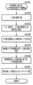
図8は、実施形態2の光集積回路の製造方法の大まかな工程を示すフロー図である。図8のフローは、図6の下側において左側から右側に向かって示した本実施形態の製造方法の概要に対応し、コア膜の堆積工程から光導波路コアの作製工程までに対応する。図8のフローは、光回路の目標の光学特性を実現するためのコア膜の初期設計値を設定する工程(S1021)で開始する。次に、初期値であるコア膜設定値によってコア膜を堆積する工程を実施する(S1022)。Figure 8 is a flow diagram showing the general steps of the manufacturing method of the optical integrated circuit of
コア膜の堆積工程が終わると、ウェハ面内で、コア膜の膜厚および屈折率をそれぞれ測定する(S1023)。この工程によって、図4の(a)、(b)に示したような、ウェハ面内におけるコア膜の膜厚および屈折率の分布データを求めることができる。S1023の工程によって、図6においては、コア膜実測値1012が得られる。ウェハにおけるコア膜の膜厚および屈折率の測定は、実施形態3で説明される光の反射スペクトル解析による多層膜の膜厚・屈折率の非接触評価によって実施できる。実施形態3の測定方法によれば、コア膜堆積前に下層酸化膜を測定し、コア膜測定時に下層酸化膜を固定して解析することで、コア膜の特性を高精度に評価することができる。詳細は、実施形態3において開示される。After the core film deposition process is completed, the film thickness and refractive index of the core film are measured within the wafer (S1023). This process makes it possible to obtain distribution data of the film thickness and refractive index of the core film within the wafer, as shown in (a) and (b) of FIG. 4. The process of S1023 obtains the actual
次に、上述のコア膜の実測値に基づいて、コア膜の膜厚および屈折率マップを作成する(S1024)。ウェハ面内のコア膜の実測値を評価する際には、後述の実施形態4の取得情報のウェハ面内フィッティングを利用することで、本工程のスループットを向上させることができる。コア膜の分布データをスパースに取得し、関数でフィッティングすることでスループットの向上可能である。ウェハ面内の分布データを均一に利用するのではなく、変化が急峻な領域(例えば、ウェハのエッジ近傍)において密にデータを取得することで、膜厚および屈折率マップの精度を向上させることができる。詳細は、実施形態4において開示される。Next, a film thickness and refractive index map of the core film is created based on the actual measured values of the core film described above (S1024). When evaluating the actual measured values of the core film within the wafer surface, the throughput of this process can be improved by using the in-wafer fitting of the acquired information of embodiment 4 described below. The throughput can be improved by sparsely acquiring the distribution data of the core film and fitting it with a function. Rather than using the distribution data within the wafer surface uniformly, the accuracy of the film thickness and refractive index map can be improved by densely acquiring data in areas where the changes are steep (e.g., near the edge of the wafer). Details are disclosed in embodiment 4.
次に、導波路コアの等価屈折率neの補正量を決定する(S1025)。この工程は、図6における補正量の決定段階1014に対応する。既に述べたように、等価屈折率は、光導波路の構造が確定して初めて算出が可能であるが、光導波路の作製工程で変更可能な光導波路の構造値に対する補正量を決定することになる。本実施形態における具体例は、後述する図9の詳細フローにおいてさらに説明される。 Next, the amount of correction for the equivalent refractive index ne of the waveguide core is determined (S1025). This step corresponds to the correction
引き続き、等価屈折率neの補正量に基づいて、コア設定値を補正する(S1026)。この工程は、図6のマスク選択段階1015に対応する。先行するS1025で決定した等価屈折率neの補正量、すなわち光導波路の構造値の補正量に対応したマスクを選択することで、光導波路のコアの設定値が補正され、推定される等価屈折率neの補正が実施される。上述のS1025~S1026の工程は、図6の「等価屈折率neの補正」に対応する。 Next, the core set value is corrected based on the correction amount of the equivalent refractive index ne (S1026). This process corresponds to the
最後に、コア設定値の補正された状態で露光およびエッチング工程を実施する(S1027)。上述の図8の工程フローでは、推定される等価屈折率neの補正と言う視点で、光集積回路の製造方法の大まかな工程を説明した。本実施形態の光集積回路の製造方法は、より具体的な工程、光導波路の構造値の補正量の例とともに、図9でさらに説明される。 Finally, exposure and etching processes are carried out in a state where the core set values have been corrected (S1027). In the process flow of Fig. 8 described above, the rough process of the manufacturing method of the optical integrated circuit has been explained from the viewpoint of correcting the estimated equivalent refractive index ne . The manufacturing method of the optical integrated circuit of this embodiment is further explained in Fig. 9 together with more specific steps and an example of the amount of correction of the structural values of the optical waveguide.
図9は、実施形態2の光集積回路の製造方法の具体的な工程を示すフロー図である。図9のフローは、図8に示した製造方法の工程において、光導波路コアの等価屈折率neの補正量の具体例として、光導波路の幅の補正量分布ΔW(x,y)を取得する例を示したものである。 Fig. 9 is a flow diagram showing specific steps of the method for manufacturing an optical integrated circuit according to
ここでまず、光導波路の構造値の補正の例として、光導波路の幅を補正する場合の幅補正量の算出について説明する。光導波路幅は、コア膜堆積の後で変更可能な構造値であり、異なる導波路幅を持った複数のマスクを予め備えておけば、ウェハ面内の位置に応じ必要な補正量にしたがってマスクを選択することで、等価屈折率neの補正を実現できる。 First, as an example of correction of the structural value of the optical waveguide, calculation of the width correction amount when correcting the width of the optical waveguide will be described. The optical waveguide width is a structural value that can be changed after the deposition of the core film, and if multiple masks with different waveguide widths are prepared in advance, the equivalent refractive index ne can be corrected by selecting a mask according to the necessary correction amount depending on the position on the wafer surface.
以下、ウェハ面内における導波路幅の補正量分布ΔW(x,y)を求める。コアの屈折率の設定値、測定値をそれぞれ、nset、n(x,y)とする。また、導波路幅の設定値、測定値をそれぞれ、Wset、W(x,y)とする。膜厚が実測されたコア膜に対して、導波路幅の設定値に与え得るべき補正量分布ΔW(x,y)は次式で定義される。
式(12)において、定数Aは、導波路幅の補正に加えて、屈折率変動が導波路幅の所要補正量に与える寄与率を意味していると考えることができる。In equation (12), the constant A can be considered to represent, in addition to the correction of the waveguide width, the contribution rate that the refractive index fluctuation has to the required correction amount of the waveguide width.
式(12)で補正量分布ΔW(x,y)を決定するために、定数Aを以下の様にして求める。本例では、光導波路の幅Wおよびコアの屈折率nの実測値が、設定値ne(Wset,nset)よりもずれた場合に、等価屈折率を補正するための幅の補正量分布量ΔW(x,y)を決定する。導波路幅およびコア屈折率をそれぞれdW、dnだけ微小変化させたときの等価屈折率は、設定値を中心に変化量が微小である前提で1次までテーラー展開することで、次式で表される。
式(13)において、微小変化した等価屈折率ne(Wset+dW,nset+dn)と設定値ne(Wset,nset)が一致するためには、式(13)の2行目においてその第2項が0となれば良いので、次式を満たせば良い。
ここで簡単のため屈折率分布n(x,y)をnで表し、等価屈折率値ne(Wset,nset)をneで表すと、定義からdn=(n-nset)となるので、式(14)は次のように変形できる。
式(15)から、さらに次式が得られる。
式(12)の導波路幅の補正量分布ΔW(x,y)の式および式(16)を参照すれば、定数Aは、次式で表される。
導波路幅の補正量分布ΔW(x,y)における定数Aの式(6)の意味するところは、定数Aは、等価屈折率のコア屈折率に対する微分値と、等価屈折率のコア導波路幅に対する微分値の比を表している。したがって定数Aは、等価屈折率の光導波路幅Wの変化に対する傾きと、等価屈折率のコア屈折率nの変化に対する傾きをそれぞれ求めれば、式(17)で決定される。定数Aは、光集積回路における光回路で、光導波路の構造およびコア膜の材料特性、作成条件が決定すれば、その条件で、等価屈折率の導波路幅W依存性、コア屈折率依存性を実測すれば良い。式(12)によって導波路幅の補正量分布ΔW(x,y)が決定できれば、図9の光集積回路の製造工程を実施することができる。The meaning of the constant A in the waveguide width correction amount distribution ΔW(x,y) in formula (6) is that the constant A represents the ratio of the derivative of the equivalent refractive index with respect to the core refractive index to the derivative of the equivalent refractive index with respect to the core waveguide width. Therefore, the constant A is determined by formula (17) by determining the slope of the equivalent refractive index with respect to the change in the optical waveguide width W and the slope of the equivalent refractive index with respect to the change in the core refractive index n. The constant A can be determined by measuring the dependence of the equivalent refractive index on the waveguide width W and the core refractive index under the conditions determined for the optical circuit in the optical integrated circuit, once the structure of the optical waveguide, the material properties of the core film, and the manufacturing conditions are determined. If the waveguide width correction amount distribution ΔW(x,y) can be determined by formula (12), the manufacturing process of the optical integrated circuit in FIG. 9 can be carried out.
図9に戻り、光導波路の幅の補正による等価屈折率の補正の例を説明すれば、図8と同様に、まずコア膜の堆積工程が実施される(S1031)。さらにウェハ面内において、コア膜の膜厚および屈折率の測定が実施される(S1032)。ここでは、実施形態3で説明される光の反射スペクトル解析による多層膜の膜厚・屈折率の非接触評価を利用できる。Returning to Figure 9, to explain an example of correcting the equivalent refractive index by correcting the width of the optical waveguide, first, as in Figure 8, a core film deposition process is performed (S1031). Furthermore, the film thickness and refractive index of the core film are measured within the wafer surface (S1032). Here, non-contact evaluation of the film thickness and refractive index of the multilayer film by light reflection spectrum analysis described in embodiment 3 can be used.
引き続き、コア膜の膜厚実測値および屈折率実測値のマップを作成が実施される(S1033)。この工程では、実施形態4で説明される取得情報のウェハ面内フィッティングの手法を利用できる。Next, a map of the actual thickness and refractive index of the core film is created (S1033). In this process, the method of in-wafer fitting of the acquired information described in embodiment 4 can be used.
コア膜の膜厚実測値および屈折率実測値が得られれば、式(12)を用いて導波路幅の補正量分布ΔW(x,y)を取得することができる(S1034)。ウェハ面内で、光導波路の幅W(構造値)の設定値が補正量分布ΔW(x,y)に基づいて補正されることで、光導波路が作製完了した時点で予測される等価屈折率は、目標の等価屈折率に近づくことになる。結果として、光回路の結果光学特性値も目標の光学特性値に近づく。Once the actual film thickness and refractive index of the core film are obtained, the waveguide width correction amount distribution ΔW(x,y) can be obtained using equation (12) (S1034). By correcting the set value of the optical waveguide width W (structural value) within the wafer surface based on the correction amount distribution ΔW(x,y), the equivalent refractive index predicted at the time when the optical waveguide is completed will approach the target equivalent refractive index. As a result, the resulting optical characteristic values of the optical circuit will also approach the target optical characteristic values.
具体的には次の工程で、取得した補正量分布ΔW(x,y)に基づいてマスクを選択すること(S1035)で、光導波路の構造値の補正が実施される。上述のS1033~S1035は、図7に示した製造システムにおける算出部1002によって実施される。Specifically, in the next step, the structural values of the optical waveguide are corrected by selecting a mask based on the acquired correction amount distribution ΔW(x,y) (S1035). The above-mentioned steps S1033 to S1035 are performed by the
最後に、選択されたマスクを使用して、図7の製造システムにおける露光・エッチング装置1003よって、露光およびエッチング工程が実施され(S1036)、光導波路の作製は終了する。Finally, using the selected mask, the exposure and etching process is carried out by the exposure/etching apparatus 1003 in the manufacturing system of Figure 7 (S1036), completing the fabrication of the optical waveguide.
したがって本開示の光集積回路の製造方法は、ウェハの面内において、コア膜の膜厚分布および屈折率分布を取得するステップ(S1032)と、前記膜厚分布および前記屈折率分布に基づいて、光導波路の構造値の補正量分布を決定するステップ(S1034)と、前記ウェハの中の1つ以上の露光単位領域に対して、前記補正量分布に対応したマスクを選択するステップ(S1035)と、前記選択されたマスクを使用して、前記ウェハの上のフォトレジスト膜を露光するステップ(S1036)とを備えるものとして実施できる。Therefore, the method for manufacturing an optical integrated circuit disclosed herein can be implemented as comprising the steps of acquiring a film thickness distribution and a refractive index distribution of a core film within the plane of a wafer (S1032), determining a correction amount distribution of a structural value of an optical waveguide based on the film thickness distribution and the refractive index distribution (S1034), selecting a mask corresponding to the correction amount distribution for one or more exposure unit areas in the wafer (S1035), and exposing a photoresist film on the wafer using the selected mask (S1036).
また本開示の光集積回路の製造システムは、ウェハの面内において、コア膜の膜厚分布および屈折率分布を取得する測定部1001と、前記膜厚分布および前記屈折率分布に基づいて、光導波路の構造値の補正量分布を決定する算出部1002と、前記ウェハの中の1つ以上の露光単位領域に対して、前記補正量分布に対応したマスクを選択し、前記選択されたマスクを使用して、前記ウェハの上のフォトレジスト膜を露光する露光部1003とを備えたものとしても実施できる。The optical integrated circuit manufacturing system disclosed herein can also be implemented as including a
上述の図9の製造工程フローでは、光導波路の構造値として導波路幅Wを補正する例を説明したが、コア膜の膜厚実測値および屈折率実測値に基づいて、予想される等価屈折率を補正できれば、構造値は幅だけに限られない。等価屈折率が異なっていてもウェハ面(x-y面)に平行な方向については、光導波路の幅だけでなく、光導波路の長さについても構造値として光信号の位相進み量の補正が可能である。式(1)で示したように、等価屈折率neの誤差により大きな影響を受けるのは、光干渉回路の光導波路における光信号の位相進み量である。 In the above-mentioned manufacturing process flow of FIG. 9, an example of correcting the waveguide width W as the structural value of the optical waveguide has been described, but the structural value is not limited to the width as long as the predicted equivalent refractive index can be corrected based on the actual thickness and refractive index of the core film. Even if the equivalent refractive index is different, in the direction parallel to the wafer surface (x-y surface), it is possible to correct the phase lead of the optical signal as a structural value not only for the width of the optical waveguide but also for the length of the optical waveguide. As shown in formula (1), it is the phase lead of the optical signal in the optical waveguide of the optical interferometer that is greatly affected by the error in the equivalent refractive index ne .
例えば光干渉回路であるMZIにおける2本のアーム導波路間の導波路長差のウェハ内バラツキは、等価屈折率のバラツキとともに干渉条件に直接影響するため問題となる。構造値として、導波路長差に対して補正をする場合は、マスクとして異なる物理長差のアーム導波路を持つ複数のマスクを備えておけば良い。コア膜の膜厚実測値および屈折率実測値から予想される等価屈折率に応じて、ウェア面内で、適切な物理長差のマスクを選択できる。このように、コア膜の実測値に基づいて補正を行う構造値は、光導波路のコア幅、光干渉回路を構成する光導波路の長さ、または、光干渉回路における光導波路間の導波路長差などを利用できる。For example, the variation in the waveguide length difference between two arm waveguides in an MZI, which is an optical interferometer, within a wafer is problematic because it directly affects the interference conditions along with the variation in the equivalent refractive index. When correcting for the waveguide length difference as a structural value, it is sufficient to provide multiple masks with arm waveguides with different physical length differences as masks. A mask with an appropriate physical length difference can be selected within the wafer surface according to the equivalent refractive index predicted from the actual measured film thickness and refractive index of the core film. In this way, the structural value for correction based on the actual measured value of the core film can be the core width of the optical waveguide, the length of the optical waveguide that constitutes the optical interferometer, or the waveguide length difference between the optical waveguides in the optical interferometer.
以下により具体的な光干渉回路において、コア膜の膜厚実測値および屈折率実測値に基づいて、光干渉回路における光導波路間の導波路長差(光路長差)を補正し、マスクの選択によって等価屈折率を補正する実施例を説明する。Below, we explain an example of a more specific optical interferometer in which the waveguide length difference (optical path length difference) between optical waveguides in an optical interferometer is corrected based on the actual measured film thickness and refractive index of the core film, and the equivalent refractive index is corrected by selecting a mask.
本実施形態の光集積回路の製造方法は、アーム導波路の導波路物理長差を、補正する「光導波路の構造値」として、光学特性である例えばAWGの中心波長のウェハ内バラツキを改善するのにも適用できる。The manufacturing method for an optical integrated circuit according to this embodiment can also be applied to improve the within-wafer variation in optical characteristics, such as the central wavelength of an AWG, by using the "structural value of the optical waveguide" to correct the difference in the physical length of the arm waveguide.
AWGでは、各アレイ導波路の光路長差に起因する位相差によって、光合分波作用を生じる。異なる波長の複数の光信号を含む波長多重化光信号を入力すれば、波長毎に光信号を異なるポートへ分離して、出力することができる。AWGにおける各出力ポートの中心波長は、アレイ導波路の光路長差に起因する位相差によって決定される。AWGのアレイ導波路における光路長差は、アレイ導波路を構成する光導波路のコアやクラッドの屈折率、コアの形状により決定される。In an AWG, the phase difference caused by the optical path length difference of each arrayed waveguide produces an optical multiplexing/demultiplexing effect. By inputting a wavelength-multiplexed optical signal containing multiple optical signals of different wavelengths, the optical signals can be separated for each wavelength and output to different ports. The central wavelength of each output port in the AWG is determined by the phase difference caused by the optical path length difference of the arrayed waveguide. The optical path length difference in the arrayed waveguide of the AWG is determined by the refractive index of the cores and cladding of the optical waveguides that make up the arrayed waveguide, and the shape of the cores.
図10は、本実施形態の光集積回路の製造方法をAWGに適用した例を説明する図である。非特許文献5を参照すれば、AWGにおける中心波長λ0の理論式は図10にも示したように次式で表される。
このように、導波路物理長差ΔLの異なる複数のAWG用のマスクを予め準備しておき、ウェハ面内において、コア膜の膜厚分布および屈折率分布から、光導波路の構造値として導波路物理長差ΔLの補正量を決定する。複数のAWG用のマスクの中から、決定されたΔLの補正量に対応したAWG用のマスクを選択することで、実質的に等価屈折率neが補正されるのと同じ効果が得られる。 In this way, a plurality of AWG masks with different waveguide physical length differences ΔL are prepared in advance, and the correction amount of the waveguide physical length difference ΔL is determined as a structural value of the optical waveguide from the film thickness distribution and refractive index distribution of the core film within the wafer surface. By selecting an AWG mask corresponding to the determined correction amount of ΔL from among the plurality of AWG masks, the same effect as that of correcting the equivalent refractive index ne can be obtained.
本実施形態の光集積回路の製造方法は、アーム導波路の光路長差を、補正する「光導波路の構造値」として、光学特性である例えばMZIの中心波長のウェハ内バラツキを改善するのにも適用できる。The manufacturing method for an optical integrated circuit according to this embodiment can also be applied to improve the within-wafer variation in optical characteristics, such as the central wavelength of an MZI, by using the optical path length difference of the arm waveguide as a "structural value of the optical waveguide" to correct the difference.
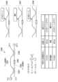
図11は、本実施形態の光集積回路の製造方法をMZIに適用した例を説明する図である。MZI1040では方向性結合器1043、1044の間に構成された2つのアーム導波路1041,1042の光路長差に起因する位相差によって、出力ポートが変化する。一方のアーム導波路1042をヒータ1045で加熱することにより、スイッチとしても活用することもできる。ここで2つのアーム導波路の光路長差ΔSが設定値からずれると、消光波長が変化する。MZIにおける2つのアーム導波路の光路長差は、光導波路を形成するコアやクラッドの屈折率、コアの形状により決定される(非特許文献5を参照)。Figure 11 is a diagram illustrating an example in which the manufacturing method of the optical integrated circuit of this embodiment is applied to an MZI. In the
非特許文献5には、2入力2出力のMZIスイッチの構造と動作原理が説明されている。MZIスイッチ1040では、2つのアーム導波路1041、1042の間の光路長差ΔSにより方向性結合器1043、1044での干渉状態が変化し、光出力強度が変化する。2つの方向性結合器の分岐比がそれぞれ50%であるとすると、2つのアーム導波路の光路長差が位相換算で0±2nπのとき入力ポート1に入力された光はすべて出力ポート2から出力される。一方、光路長差が位相換算でπ±2nπのとき入力ポート1に入力された光はすべて出力ポート1から出力される。MZI透過スペクトルの理論式は、非特許文献6にも開示されている。Non-Patent Document 5 describes the structure and operation principle of a two-input, two-output MZI switch. In the
非特許文献6によれば、光を入力ポート1から入力した場合の出力ポート3の出力P3は次式で表される。
本実施形態の光集積回路の製造方法をMZIへ適用するには、ウェハ面内のコア膜の実測値分布から予測される等価屈折率neに合わせて、アーム導波路間の物理長差(L1-L2)を選択すれば良い。具体的には図11の表に示したように、予測される等価屈折率neが等価屈折率の設定値よりもやや小さい場合は、光路長差ΔSは式(19)から短くなってしまう。そこで、物理長差(L1-L2)がより大きいマスク1048を選択すれば良い。逆に予測される等価屈折率neが等価屈折率の設定値よりもやや大きい場合は、光路長差ΔSは式(19)から長くなってしまう。この場合は、物理長差(L1-L2)がより小さいマスク1046を選択すれば良い。等価屈折率の設定値からの逸脱が無く、設計値通りであれば、標準の物理長差(L1-L2)の標準マスク1047を使用すれば良い。 To apply the manufacturing method of the optical integrated circuit of this embodiment to the MZI, the physical length difference (L 1-L2 ) between the arm waveguides may be selected in accordance with the equivalent refractive index ne predicted from the measured distribution of the core film in the wafer surface. Specifically, as shown in the table of FIG. 11, when the predicted equivalent refractive index ne is slightly smaller than the set value of the equivalent refractive index, the optical path length difference ΔS becomes shorter according to the formula (19). Therefore, the
このように、予め物理長差(L1-L2)の異なる複数のMZI用のマスクを準備しておき、ウェハ面内において、コア膜の膜厚分布および屈折率分布から、光導波路の構造値として物理長差(L1-L2)の補正量を決定する。複数のMZI用のマスクから、決定された物理長差(L1-L2)の補正量に対応したマスクを選択することで、実質的に等価屈折率neが補正されるのと同じ効果が得られる。 In this way, a plurality of masks for MZIs with different physical length differences (L1 -L2 ) are prepared in advance, and the correction amount of the physical length difference (L1 -L2 ) is determined as the structural value of the optical waveguide from the film thickness distribution and refractive index distribution of the core film within the wafer surface. By selecting a mask corresponding to the determined correction amount of the physical length difference (L1 -L2 ) from the masks for the plurality of MZIs, the same effect as that of correcting the equivalent refractive index ne can be obtained.
以上詳細に述べたように、本開示の光集積回路の製造方法によって、コア膜の堆積工程で生じる誤差の分布データが直ちに後工程である光導波路の作製工程に反映さる。図3とともに実施形態1で説明をしたフィードフォワードシステムが実現される。ウェハ面内で生じる光学特性のバラツキを抑えた、光集積回路の製造工程が実現される。光集積回路の製造工程の効率化、高スループット化を実現できる。As described in detail above, the manufacturing method for optical integrated circuits disclosed herein allows distribution data of errors occurring in the core film deposition process to be immediately reflected in the subsequent optical waveguide fabrication process. The feedforward system described in
[実施形態3]
本実施形態のフィードフォワードシステムにおいて、各々の工程における膜厚、屈折率を非接触により測定する方法について、以下に説明する。[Embodiment 3]
A method for non-contact measurement of the film thickness and refractive index in each process in the feedforward system of this embodiment will be described below.
[3.1 測定装置]
図12は、本発明の一実施形態にかかる測定装置の概略の構成を示す図である。測定装置は、製造対象物である光デバイスにレーザ光を照射し、対象物からの反射光を解析して、非接触により、光デバイスに形成されている膜の物性値、例えば膜厚、屈折率を測定する。測定原理として、従来の分光反射式膜厚計、分光エリプソメーターなどの測定方式を適用することができる。3.1 Measurement Equipment
12 is a diagram showing a schematic configuration of a measuring device according to one embodiment of the present invention. The measuring device irradiates an optical device, which is an object to be manufactured, with laser light, analyzes the reflected light from the object, and measures the physical properties of a film formed on the optical device, such as film thickness and refractive index, in a non-contact manner. As a measurement principle, a measurement method such as a conventional spectroscopic reflection type film thickness meter or a spectroscopic ellipsometer can be applied.
測定装置は、光学測定系101とテスタ102とにより構成されている。測定対象となる光デバイスが形成されたシリコンウェハ114は、ウェハチャック113に固定され、基台111上の駆動機構112によって、3軸方向に移動させられる。テスタ102に接続されたテストヘッド121は、送光光学系122、受光光学系123および制御回路124を備えている。テスタ1は、シリコンウェハ114に形成されている光デバイスを構成する膜の所望の位置に、送光光学系122からのレーザ光を照射するように、駆動機構112を制御し、テストヘッド121の制御回路124に指令を送出する。対象物からの反射光を受光光学系123により受光し、制御回路124は、受光光学系123からの信号を処理して、測定結果をテスタ1に送り返す。The measurement device is composed of an
テスタ1は、後述するように、受光光学系123からの信号を解析して、シリコンウェハ114に形成されている各膜の物性値を算出する。As described below, the
[3.2 膜厚、屈折率の非接触測定法]
例えば、図1および図2の下部クラッド堆積工程1で形成される下部クラッド12を、分光反射式で測定する場合を説明する。テスタ1は、テストヘッド121の送光光学系122から、下部クラッド12の表面に対して、所定の入射角で波長掃引範囲450-900nmのレーザ光を照射する。受光光学系123で受光した光の光強度から、テスタ1は、波長に対する反射率で表された反射スペクトルを算出する。[3.2 Non-contact measurement method for film thickness and refractive index]
For example, a case will be described in which the
図13は、本実施形態の測定装置による下部クラッドの反射スペクトルを示す図である。送光光学系122から出射されたレーザ光は、下部クラッド12の表面と、基板11および下部クラッド12の界面とにおいて反射し、受光光学系123には、両者が干渉した反射光が入射される。この光の干渉が反射スペクトルに反映され、膜が均一に形成されていれば、干渉により波打ったスペクトルが観測される。膜厚が薄い場合は、波の幅は大きくなり(波の数は少なくなり)、膜厚が厚い場合は、波の幅は小さくなる(波の数は多くなる)。テスタ1は、この反射スペクトルの波の振幅、周期から下部クラッド12の膜厚と屈折率とを算出することができる。Figure 13 shows the reflection spectrum of the lower clad measured by the measuring device of this embodiment. The laser light emitted from the light-transmitting
図14を参照して、下部クラッドの膜厚および屈折率の算出方法を説明する。送光光学系122からの入射光の強度E0、下部クラッド12の表面から反射された反射光の強度E1、基板11と下部クラッド12の界面とにおいて反射された反射光の強度E2とする。さらに、下部クラッド12および基板11と下部クラッド12の界面の間を往復して、下部クラッド12の表面から出射される反射光をE3,E4,...、受光光学系123に入射される反射光全体の光強度Eとすると、次式の関係が成り立つ。
ここで、rijは屈折率niのi番目の層(0は空気中)からの入射光が屈折率njのj番目の層との界面で反射したときの反射率であり、rij=-rjiである。また、tijはi層とj層の界面をi層からj層に透過したときの透過率であり、tjiはその逆であり、i番目の層の膜厚di、屈折率ni、波長λとしたとき、i番目の層を往復したときの位相係数Δiは、次式である。
このとき、TE(P)波に対する反射率r12および透過率t12は、次式となる。
また、TM(S)波に対する反射率r12および透過率t12は、次式となる。
上式をマクローリン展開から整理して、1番目の層である下部クラッド12からの反射光全体の反射率r1は、次式となる。
次に、反射率r1の波長依存性、すなわち反射スペクトルの振幅、周期から、下部クラッド12の膜厚d1と屈折率n1とを算出する。 Next, the film thicknessd1 and refractive indexn1 of the
[3.3 多段階測定法]
次に、図1および図2のコア堆積工程2で形成されるコア13を、分光反射式で測定する場合を説明する。上述した送光光学系122から出射されたレーザ光は、コア13の表面、コア13と下部クラッド12の界面、および基板11と下部クラッド12の界面において反射する。分光反射式で測定する場合、基板11と下部クラッド12の界面からの反射光はノイズとなるので、膜厚と屈折率の算出に際しては除去する必要がある。一方、石英系平面光波回路では、コア13と下部クラッド12との屈折率差は1%程度と小さいため、コア13と下部クラッド12の界面における反射率よりも、基板11と下部クラッド12の界面における反射率の方が高い。加えて、コア13の膜厚は数μm程度と薄いため、基板11と下部クラッド12の界面からの反射光の成分が大きく、膜厚と屈折率の算出が困難である。3.3 Multi-stage measurement method
Next, a case where the core 13 formed in the
そこで、本実施形態では、多層膜を形成する製造工程において、前工程で測定した結果を、現在の工程の測定結果に反映させる多段階測定法を適用する。Therefore, in this embodiment, in the manufacturing process of forming a multilayer film, a multi-stage measurement method is applied in which the results of measurement in the previous process are reflected in the measurement results of the current process.
図15は、本発明の一実施形態にかかる多層膜の測定方法を示す図である。コア堆積工程2で形成されるコア13を、分光反射式で測定する場合を説明する。前工程の下部クラッド堆積工程1で形成される下部クラッド12の測定結果を取得する。反射スペクトルは図13に示した通りであり、ここから得られた下部クラッド12の物性値(n,d)、ここでは屈折率と膜厚を取得する(S141)。次に、コア堆積工程2で形成されるコア13の測定結果を取得する(S142)。Figure 15 is a diagram showing a method for measuring a multilayer film according to one embodiment of the present invention. This explains the case where the core 13 formed in the
図16は、本実施形態の測定装置によるコアの反射スペクトルを示す図である。上述したように、コア13の測定結果は、コア13と下部クラッド12との屈折率差が小さいため、図16に示すように、反射スペクトルの包絡線にゆらぎが生じる。Figure 16 shows the reflection spectrum of the core measured by the measurement device of this embodiment. As described above, the measurement result of the core 13 shows that the reflection spectrum envelope fluctuates because the refractive index difference between the core 13 and the
図17は、コアの膜厚および屈折率の算出方法を説明する図である。送光光学系122からの入射光に対して、受光光学系123に入射される反射光全体の光強度Etotalは、次式となる。
さらに、上部クラッド19を形成するなど、3つ以上の層を形成する場合には、前工程の測定結果である膜厚と屈折率とを定数として反射率を求め、反射率の波長依存性を解析し、現在の工程の膜厚と屈折率の解を求める。例えば、基板上に4つの層を積層し、最後の工程で形成した層の膜厚と屈折率を算出する場合を考える。最初の工程で形成した層からの反射光全体の反射率r4を定数として、2番目の工程で形成した層の反射率r3+4を求め、さらに、3番目の工程で形成した層の反射率r2+3+4を求める。最後の工程で形成した層の反射率r1+2+3+4から、反射率の波長依存性を解析し、最後の工程で形成した4番目の層の膜厚と屈折率の解を求める。
本実施形態によれば、多層膜を形成する製造工程において、各々の工程における膜厚、屈折率を非接触により測定し、その差分を解析することにより、各工程で形成された膜の物性値を取得することができる。According to this embodiment, in the manufacturing process for forming a multilayer film, the film thickness and refractive index at each process are measured non-contact and the differences are analyzed to obtain the physical properties of the film formed at each process.
[3.4 温度情報の活用]
屈折率の測定は、測定時の温度によって左右される。例えば、基板材料であるSiO2は、線膨張係数が約0.5×10⁻⁶(室温~1000℃)、屈折率変化率約10-5/Kである。一般的に、光信号処理を行う光デバイスでは、屈折率を10-5程度の精度で制御する必要があるために、温度情報を活用した測定値の補正は有益である。[3.4 Use of temperature information]
The measurement of the refractive index depends on the temperature at the time of measurement. For example, the linear expansion coefficient ofSiO2 , which is the substrate material, is about 0.5×10⁻⁶ (room temperature to 1000°C), and the refractive index change rate is about 10-5 /K. In general, in optical devices that perform optical signal processing, the refractive index needs to be controlled with an accuracy of about 10-5 , so it is useful to correct the measurement value using temperature information.
本実施形態の測定装置においては、ウェハチャック113の上面に、複数のサーミスタを配置して、シリコンウェハ114の任意の位置の温度を測定する。下部クラッド12、コア13の屈折率を算出する際に、測定された温度から、上記の温度に対する屈折率変化率を加味して算出する。また、膜厚を算出する際に、測定された温度から、上記の線膨張係数を加味して算出する。In the measuring device of this embodiment, multiple thermistors are placed on the upper surface of the
ウェハにおける温度の測定点は、所定の間隔で設けてもよいし、ウェハに形成される光回路1チップごとに、所定の測定点を設けてもよい。さらに、1チップの中に形成される機能部品、屈折率変換に影響を受け易い機能部品ごとに測定点を設けることが好適である。この場合、上述した反射率の測定における測定点も、温度測定の測定点と同じとする。Temperature measurement points on the wafer may be set at a predetermined interval, or a predetermined measurement point may be set for each optical circuit chip formed on the wafer. Furthermore, it is preferable to set a measurement point for each functional component formed in one chip, and for each functional component that is easily affected by refractive index change. In this case, the measurement points for the reflectance measurement described above are the same as the measurement points for the temperature measurement.
例えば、代表的な光回路であるアレイ導波路格子(AWG)について説明する。AWGは、入力導波路に接続された入力スラブ導波路と出力導波路に接続された出力スラブ導波路との間を、それぞれの物理的な導波路長の差がΔLの複数のアレイ導波路で接続している。AWGの光学特性のうち、中心波長λ0は、既に述べたように次式で決定される。
ここで、ncはアレイ導波路の実効屈折率、mは回折次数である。アレイ導波路の実効屈折率は、クラッドとコアの膜厚によって決定され、その均一性が干渉特性に影響を与える。このため、製造誤差が中心波長の精度に与える影響が大きい。従って、複数のアレイ導波路を精度よく均一に作製するために、例えば、入力スラブ導波路、アレイ導波路の中間地点、出力スラブ導波路の付近において、温度の測定点を設け、温度分布を導出しておく。このように屈折率の測定精度を担保することにより、後工程の製造条件を調整ないし補正を行う精度も向上させることが可能となる。 Here, nc is the effective refractive index of the arrayed waveguide, and m is the diffraction order. The effective refractive index of the arrayed waveguide is determined by the film thickness of the cladding and core, and its uniformity affects the interference characteristics. For this reason, manufacturing errors have a large effect on the accuracy of the central wavelength. Therefore, in order to manufacture a plurality of arrayed waveguides with high accuracy and uniformity, for example, temperature measurement points are provided near the input slab waveguide, the midpoint of the arrayed waveguide, and the output slab waveguide, and the temperature distribution is derived. By ensuring the measurement accuracy of the refractive index in this way, it is possible to improve the accuracy of adjusting or correcting the manufacturing conditions in the subsequent process.
[3.5 機械学習による特性予想]
上述した温度の測定結果は、機械学習による物性値の予想に必要なデータとして格納しておくことが考えられる。取得した温度情報からウェハチャック113上に固定されたシリコンウェハ114の温度分布を算出することにより、サーミスタが配置されていない光回路の任意の位置の温度も取得することができ、より正確な屈折率、膜厚の補正を行うことができる。[3.5 Property prediction using machine learning]
The above-mentioned temperature measurement results can be stored as data necessary for predicting physical property values by machine learning. By calculating the temperature distribution of the
温度分布を算出する上で、フィッティングに必要な関係式が不明であっても、実測データを教師データとして、中心波長に対する導波路幅、高さなど、相関のある特徴量と合わせて学習させることにより、温度分布を算出することができる。Even if the relationship equation required for fitting to calculate the temperature distribution is unknown, the temperature distribution can be calculated by using actual measured data as training data and learning it together with correlated features such as the waveguide width and height relative to the central wavelength.
本実施形態は、基板上に形成された多層膜の各膜の物性値を測定する多層膜の非接触測定法において、前工程で得られた第1の膜の第1の測定結果を取得するステップであって、前記第1の測定結果は、前記第1の膜の表面に照射したレーザ光の当該表面からの反射光の光強度である、ステップと、現在の工程で形成された第2の膜の第2の測定結果を取得するであって、前記第2の測定結果は、前記第2の膜の表面に照射したレーザ光の当該表面からの反射光の光強度である、ステップと、前記第2の測定結果と前記第1の測定結果の差分であって、前記反射光の光強度から求めた、波長に対する反射率で表された反射スペクトルの差分を算出するステップと、前記差分から前記第2の膜の膜厚および屈折率を算出するステップとを備えたものとして実施できる。This embodiment can be implemented as a non-contact measurement method for a multilayer film for measuring the physical properties of each film of a multilayer film formed on a substrate, comprising the steps of: acquiring a first measurement result of a first film obtained in a previous process, the first measurement result being the light intensity of reflected light from the surface of the first film of laser light irradiated onto the surface of the first film; acquiring a second measurement result of a second film formed in a current process, the second measurement result being the light intensity of reflected light from the surface of the second film of laser light irradiated onto the surface of the second film; calculating the difference between the second measurement result and the first measurement result, which is the difference in the reflection spectrum expressed in terms of reflectance versus wavelength obtained from the light intensity of the reflected light; and calculating the film thickness and refractive index of the second film from the difference.
また上記の非接触測定法は、前記基板の任意の位置の温度を測定するステップをさらに備え、前記膜厚および前記屈折率を算出するステップは、温度による補正をさらに行うことを特徴とする。The above non-contact measurement method further includes a step of measuring the temperature at any position on the substrate, and the step of calculating the film thickness and the refractive index further includes a correction based on temperature.
[実施形態4]
本実施形態では、実施形態3の非接触測定を、さらに製造工程のスループットの低下を生じさせずに効率的に実施するための方法を提示する。[Embodiment 4]
In this embodiment, a method for efficiently performing the non-contact measurement of the third embodiment without causing a decrease in the throughput of the manufacturing process will be presented.
ウェハ上に複数形成される同一の光デバイスは、均一な特性、機能を発現できなければならない。しかしながら、製造工程においては、上述したように、ウェハ面内の温度分布により特性の変動が避けられないばかりか、半導体材料の堆積、エッチングなどの加工精度のばらつきによっても、特性の変動が避けられない。従って、光学特性などの特性の検査においては、ウェハ上の測定点が多いほど、製造誤差を抑制することができるが、測定点の増大は、製造工程のスループットを低下させてしまう。Multiple identical optical devices formed on a wafer must be able to exhibit uniform characteristics and functions. However, in the manufacturing process, as mentioned above, not only are fluctuations in characteristics inevitable due to temperature distribution across the wafer, but also due to variations in processing accuracy such as deposition and etching of semiconductor materials. Therefore, when inspecting characteristics such as optical characteristics, the more measurement points there are on the wafer, the more manufacturing errors can be suppressed, but an increase in the number of measurement points reduces the throughput of the manufacturing process.
そこで本実施形態では、製品ロットの製造の前に、試作ロットの検査においてフィッティング処理を行い、予めウェハ上の測定点を特定し、かつ測定点の数を減らすことにより、製造工程のスループットの低下を防ぐ。以下、フィッティング処理の詳細を説明する。Therefore, in this embodiment, a fitting process is performed in the inspection of a prototype lot before the production of a product lot, and measurement points on the wafer are identified in advance, and the number of measurement points is reduced, thereby preventing a decrease in throughput of the manufacturing process. The details of the fitting process are explained below.
試作ロットにおいて、上述した測定装置により、例えば、図1および図2の下部クラッド堆積工程1で形成される下部クラッド12を、ウェハ全体にわたって、所定の間隔で反射率を測定する。テスタ1は、測定結果の反射スペクトルから膜厚と屈折率とを算出する。ここで再び図4の(b)の1次元の屈折率分布を参照する。図4の(b)では、直径300mmのウェハの中心を座標x=0,y=0とし、y=0の直線上を2mm間隔で測定し、求めた屈折率が白丸で示されている。横軸(x軸)は、中心から距離であり、縦軸が屈折率である。In a prototype lot, the reflectance of the
同様にして、y軸方向に2mm間隔でy軸に平行な複数の直線上を測定することにより、ウェハ全体にわたって2mmのメッシュ間隔で測定を行う。この測定結果から、ウェハ上の任意の位置の屈折率の近似式n(x,y)および膜厚の近似式t(x,y)を、次式にて生成する。
上記2つの近似式で、ak,bk,ck,dkは係数であり、最小二乗法等を用いて求めることができる。図4の(b)に示した実線は、この近似式で表されるフィッティング関数であって、y=0の直線上の屈折率n(x,y)のフィッティング結果を表している。図4の(b)では屈折率に対してのフィッティングを示したが、膜厚についても同様のことができる。 In the above two approximate expressions, ak , bk , ck , and dk are coefficients, which can be found using the least squares method, etc. The solid line shown in Fig. 4B is a fitting function expressed by this approximate expression, and shows the fitting result of the refractive index n(x, y) on the straight line where y = 0. Fig. 4B shows fitting for the refractive index, but the same can be done for the film thickness.
図4の(a)を再び参照すると、フィッティング処理の結果を示している。ウェハ全体にわたるフィッティング処理の結果を、3次元的に表した図であり、ウェハの中心をx=0,y=0とする2次元平面における光学膜厚(屈折率×膜厚)を表している。なお、近似式は、試作ロットの1枚のウェハから求めても良いし、複数枚のウェハから求めた結果の平均を用いても良い。また、ウェハの基板面内の測定点は、メッシュ状に設定する必要はなく、任意ではあるが、図8からも分かるように、フィッティング処理においては、測定点が多いほど近似式の精度が向上する。図4の(a)では光学膜厚に対して3次元的なフィッティングの例を示したが、屈折率または膜厚についても、同様にフィッティング処理を行って3次元的に表すことができる。Referring again to FIG. 4(a), the result of the fitting process is shown. It is a three-dimensional representation of the result of the fitting process over the entire wafer, and shows the optical film thickness (refractive index x film thickness) in a two-dimensional plane with the center of the wafer at x = 0, y = 0. The approximation formula may be obtained from one wafer of a prototype lot, or the average of the results obtained from multiple wafers may be used. Also, the measurement points in the substrate surface of the wafer do not need to be set in a mesh pattern and are arbitrary, but as can be seen from FIG. 8, in the fitting process, the more measurement points there are, the higher the accuracy of the approximation formula will be. FIG. 4(a) shows an example of three-dimensional fitting for the optical film thickness, but the refractive index or film thickness can also be represented three-dimensionally by performing a similar fitting process.
図18は、測定点の数と屈折率の測定精度との関係を示す図である。1回のみの測定で得られる単一の測定結果における測定精度を、規格化した1として点線により示している。ウェハ上の測定点が増えたとしても、測定精度は変わらず一定である。測定点を増やしてフィッティング処理を行うと、同一の測定点を複数回測定して平均値を出す方法と同様の効果があり、実線に示すように測定精度が向上する。これは、サンプル数が多いほど標本平均の分布における平均は母平均に近づき、標本平均の分布における標本分散は母分散の1/nに近づくという中心極限定理による精度向上と同じ原理による。すなわち、ある単一の測定点における測定結果は、周辺の測定点の結果をもとに、ランダムに発生する測定ばらつきを抑制できるために測定精度が向上する。Figure 18 shows the relationship between the number of measurement points and the measurement accuracy of the refractive index. The measurement accuracy of a single measurement result obtained by only one measurement is shown by a dotted line as a normalized value of 1. Even if the number of measurement points on the wafer increases, the measurement accuracy remains constant. Increasing the number of measurement points and performing fitting processing has the same effect as the method of measuring the same measurement point multiple times and obtaining the average value, and the measurement accuracy improves as shown by the solid line. This is due to the same principle as the improvement in accuracy due to the central limit theorem, which states that the more samples there are, the closer the average in the distribution of sample averages becomes to the population mean, and the closer the sample variance in the distribution of sample averages becomes to 1/n of the population variance. In other words, the measurement accuracy of a single measurement point is improved because the measurement results can suppress randomly occurring measurement variations based on the results of surrounding measurement points.
次に、測定点を特定する方法について説明する。第1に、所望の測定精度を設定し、図18に示した結果から、ウェハ内の測定点の数を決定する。例えば、直径300mmのウェハ全体を、上述したように2mmのメッシュ間隔で測定すると、測定点は18,000点程度になる。所定の測定精度を、規格化された値で0.25以下とすると、図18に示したように、測定点が200点以上あれば、測定精度を満たすことができる。このとき、製造工程(例えば、下部クラッド堆積工程1)において許容されている時間のうち、測定に割り当てられた時間を、1測定点にかかる測定時間で除して得られた測定回数の上限から、測定点の数を決定しても良い。第2に、特定の位置の測定点を選択する。Next, a method for identifying the measurement points will be described. First, a desired measurement accuracy is set, and the number of measurement points in the wafer is determined from the results shown in FIG. 18. For example, if the entire wafer with a diameter of 300 mm is measured with a mesh interval of 2 mm as described above, the number of measurement points will be about 18,000. If the predetermined measurement accuracy is set to a standardized value of 0.25 or less, as shown in FIG. 18, the measurement accuracy can be satisfied if there are 200 or more measurement points. At this time, the number of measurement points may be determined from the upper limit of the number of measurements obtained by dividing the time allocated to measurement among the time allowed in the manufacturing process (for example, the lower cladding deposition process 1) by the measurement time required for one measurement point. Second, a measurement point at a specific position is selected.
図19は、フィッティング処理の結果、実際に測定する測定点を示した図である。測定点は、ウェハ上に形成される光デバイスの位置に関係なく選択することができる。例えば、図4の(a)、(b)に示したフィッティング処理の結果から、近似式とよく整合している測定点を選択することが考えられる。また、近似式で表されるフィッティング関数の変曲点付近に測定点を密に設定することも考えられる。さらに、製造工程におけるウェハ上の温度分布、製造誤差のバラツキなどを考慮して設定することもできる。一方、光デバイスに含まれる光機能回路に、精度の要求される回路が含まれる場合に、当該光機能回路が形成される位置を、測定点として選択することもできる。Figure 19 shows the measurement points that are actually measured as a result of the fitting process. The measurement points can be selected regardless of the position of the optical device formed on the wafer. For example, it is possible to select measurement points that are well consistent with the approximation formula from the results of the fitting process shown in (a) and (b) of Figure 4. It is also possible to set the measurement points densely near the inflection points of the fitting function represented by the approximation formula. Furthermore, it is also possible to set them taking into account the temperature distribution on the wafer during the manufacturing process, the variation in manufacturing errors, etc. On the other hand, if the optical functional circuit included in the optical device includes a circuit that requires precision, the position where the optical functional circuit is formed can also be selected as the measurement point.
製品ロットの製造においては、フィッティング処理によって求めた測定点のみ測定を行う。次の製造工程(例えば、コア堆積工程2)には、この測定点における測定結果と、フィッティング処理の結果とが渡され、次の製造工程の製造条件が求められる。後工程においては、フィッティング処理の結果が優先して用いられる。試作ロットにおける測定結果の分布が滑らかであり、フィッティング処理の結果、適当な関数で近似式が表される場合には、上述したように、単一の測定結果よりもフィッティング処理の結果の方が、測定精度が高いからである。When manufacturing a product lot, measurements are taken only at the measurement points determined by the fitting process. The measurement results at these measurement points and the results of the fitting process are passed to the next manufacturing process (e.g., core deposition process 2), and the manufacturing conditions for the next manufacturing process are determined. In subsequent processes, the results of the fitting process are used preferentially. This is because, when the distribution of measurement results in a prototype lot is smooth and the fitting process results can be approximated by an appropriate function, as mentioned above, the results of the fitting process have higher measurement accuracy than a single measurement result.
本実施形態の非接触測定法は、基板上に形成された膜の物性値を測定する非接触測定法であって、前記基板面内の任意の第1の測定点における測定結果から前記基板面内の物性値の分布を表す近似式を求める第1ステップと、前記第1の測定点より数が少なく、特定の位置の第2の測定点を選択する第2ステップとを含むフィッティング工程を予め実行し、前記膜の製造工程において、前記第2の測定点において測定した測定結果と前記近似式とを用いて、前記膜の物性値を測定することを特徴とするものとして実施できる。The non-contact measurement method of this embodiment is a non-contact measurement method for measuring the physical property values of a film formed on a substrate, and can be implemented by performing in advance a fitting process including a first step of obtaining an approximate equation representing the distribution of the physical property values within the substrate surface from the measurement results at any first measurement point within the substrate surface, and a second step of selecting second measurement points that are fewer in number than the first measurement points and are located at specific positions, and by measuring the physical property values of the film in the manufacturing process of the film using the measurement results measured at the second measurement points and the approximate equation.
前記測定結果は、前記膜の表面に照射したレーザ光の当該表面からの反射光の光強度であり、前記物性値は、前記膜の膜厚および屈折率であることを特徴とする。The measurement result is the light intensity of the laser light reflected from the surface of the film, and the physical property values are the film thickness and refractive index of the film.
また本実施形態の別の非接触測定法は、基板上に形成された多層膜の各膜の物性値を測定する多層膜の非接触測定法であって、前記各膜の任意の第1の測定点における測定結果から前記基板面内の物性値の分布を表す近似式を求める第1ステップと、前記第1の測定点より数が少なく、特定の位置の第2の測定点を選択する第2ステップとを含むフィッティング工程を予め実行し、前記多層膜の製造工程において、前工程で得られた第1の膜の第1の測定結果を取得するステップであって、前記第1の測定結果は、前記第1の膜に対する前記フィッティング工程における第2の測定点において測定した測定結果と近似式とを含む、ステップと、現在の工程で形成された第2の膜の第2の測定結果を取得するステップと、前記第2の測定結果と前記第1の測定結果との差分を算出するステップであって、前記第2の測定結果と前記第2の測定点において測定した測定結果との差分、または前記第2の測定結果と前記近似式から得られた前記第2の測定結果の測定点に対応する測定結果との差分を求める、ステップと、前記差分から前記第2の膜の物性値を算出するステップとを備えるものとして実施できる。Another non-contact measurement method of this embodiment is a non-contact measurement method of a multilayer film for measuring the physical property values of each film of a multilayer film formed on a substrate, which includes a fitting process including a first step of obtaining an approximate equation representing the distribution of physical property values within the substrate surface from the measurement results at any first measurement point of each film, and a second step of selecting second measurement points at specific positions that are fewer in number than the first measurement points, and can be implemented as including the steps of: acquiring a first measurement result of a first film obtained in a previous process in a manufacturing process of the multilayer film, the first measurement result including a measurement result measured at a second measurement point in the fitting process for the first film and an approximate equation; acquiring a second measurement result of a second film formed in a current process; and calculating a difference between the second measurement result and the first measurement result, the difference between the second measurement result and the measurement result measured at the second measurement point, or the difference between the second measurement result and the measurement result corresponding to the measurement point of the second measurement result obtained from the approximate equation; and calculating the physical property value of the second film from the difference.
上記別の非接触測定法において、前記第1および前記第2の測定結果は、前記第1および前記第2の膜の表面に照射したレーザ光の当該表面からの反射光の光強度であることを特徴とする。また、上記別の非接触測定法において、前記差分は、前記反射光の光強度から求めた、波長に対する反射率で表された反射スペクトルの差分であることを特徴とする。前記物性値は、前記第1および前記第2の膜の膜厚および屈折率であり得る。In the above-mentioned another non-contact measurement method, the first and second measurement results are the light intensity of the reflected light from the surfaces of the first and second films of laser light irradiated onto the surfaces. In the above-mentioned another non-contact measurement method, the difference is the difference in the reflection spectrum expressed as the reflectance against the wavelength, calculated from the light intensity of the reflected light. The physical property value may be the film thickness and the refractive index of the first and second films.
本実施形態では、製品ロットの製造の前の試作ロットの検査において、1または複数のウェハを用いてフィッティング処理を行う方法を説明した。製品ロットの製造工程に入った後においても、製品ロットの製造において得られた測定結果と、予め求めたフィッティング処理の結果とを比較して、近似式を随時変更するようにしても良い。In this embodiment, a method for performing fitting processing using one or more wafers in the inspection of a prototype lot prior to the manufacture of a product lot has been described. Even after the manufacturing process of the product lot has begun, the measurement results obtained in the manufacture of the product lot may be compared with the results of the fitting processing obtained in advance, and the approximation formula may be changed as needed.
本実施形態よれば、フィッティング処理により予めウェハ上の測定点を特定し、かつ測定点の数を減らすことにより、測定精度を落とすことなく、製造工程のスループットの低下を防ぐことができる。According to this embodiment, by identifying measurement points on the wafer in advance through a fitting process and reducing the number of measurement points, it is possible to prevent a decrease in throughput of the manufacturing process without sacrificing measurement accuracy.
Claims (10)
Translated fromJapanese前記膜厚分布および前記屈折率分布に基づいて、光導波路の構造値の補正量分布を決定するステップであって、前記構造値は、光干渉回路を構成する前記光導波路の長さ、または、前記光干渉回路における前記光導波路の間の導波路長差の少なくともいずれかを含む、ステップと、
前記ウェハの中の1つ以上の露光単位領域に対して、前記補正量分布に対応したマスクを選択するステップと、
前記選択されたマスクを使用して、前記ウェハの上のフォトレジスト膜を露光するステップと
を備えることを特徴とする光集積回路の製造方法。 acquiring a thickness distribution and a refractive index distribution of a core film within a surface of a wafer;
determining a correction amount distribution of a structural value of an optical waveguide based on the film thickness distribution and the refractive index distribution, the structural value including at least one of a length of the optical waveguide constituting an optical interferometer and a waveguide length difference between the optical waveguides in the optical interferometer;
selecting a mask corresponding to the correction amount distribution for one or more exposure unit areas in the wafer;
and exposing a photoresist film on the wafer using the selected mask.
前記ウェハに少なくとも1つの前記露光単位領域が含まれることを特徴とする請求項1に記載の光集積回路の製造方法。 the exposure unit area includes an optical interference circuit having two or more optical waveguides,
2. The method for producing an optical integrated circuit accordingto claim 1 , wherein the wafer includes at least one of the exposure unit areas.
基板上に形成された多層膜の各膜の物性値を測定する多層膜の非接触測定法によって実施され、当該非接触測定法は、
前工程で得られた第1の膜の第1の測定結果を取得するステップであって、前記第1の測定結果は、前記第1の膜の表面に照射したレーザ光の当該表面からの反射光の光強度である、ステップと、
現在の工程で形成された第2の膜の第2の測定結果を取得するステップであって、前記第2の測定結果は、前記第2の膜の表面に照射したレーザ光の当該表面からの反射光の光強度である、ステップと、
前記第2の測定結果と前記第1の測定結果の差分であって、前記反射光の光強度から求めた、波長に対する反射率で表された反射スペクトルの差分を算出するステップと、
前記差分から前記第2の膜の膜厚および屈折率を算出するステップ
を含むことを特徴とする請求項1または2に記載の光集積回路の製造方法。The step of acquiring a thickness distribution and a refractive index distribution of the core film includes:
The method is carried out by a non-contact measurement method for a multilayer film that measures the physical properties of each film of a multilayer film formed on a substrate, and the non-contact measurement method includes:
A step of acquiring a first measurement result of a first film obtained in a previous step, the first measurement result being a light intensity of a laser beam irradiated onto a surface of the first film and reflected from the surface;
acquiring a second measurement result of a second film formed in a current process, the second measurement result being a light intensity of a laser beam irradiated onto a surface of the second film and reflected from the surface;
calculating a difference between the second measurement result and the first measurement result, the difference being a reflection spectrum difference expressed as a reflectance with respect to a wavelength obtained from the light intensity of the reflected light;
calculating a thickness and a refractive index of the second film from the difference;
3. The method for producing an optical integrated circuit according to claim 1, further comprising :
基板上に形成された膜の物性値を測定する非接触測定法によって実施され、当該非接触測定法は、
基板面内の任意の第1の測定点における測定結果から前記基板面内の物性値の分布を表す近似式を求める第1ステップと、
前記第1の測定点より数が少なく、特定の位置の第2の測定点を選択する第2ステップとを含むフィッティング工程を予め実行し、
前記膜の製造工程において、前記第2の測定点において測定した測定結果と前記近似式とを用いて、前記膜の物性値を測定することを特徴とする請求項1または2に記載の光集積回路の製造方法。The step of acquiring a thickness distribution and a refractive index distribution of the core film includes:
The method is carried out by a non-contact measurement method for measuring the physical properties of a film formed on a substrate, the non-contact measurement method comprising:
A first step of obtaining an approximation expression representing a distribution of a physical property value in a substrate plane from a measurement result at an arbitrary first measurement point in the substrate plane;
a second step of selecting second measurement points, the second measurement points being less in number than the first measurement points and located at specific positions;
3. The method for manufacturing an optical integrated circuit according to claim 1, wherein in the film manufacturing process, a physical property value of the film is measured using a measurement result measured at the second measurement point and the approximation formula .
ウェハの面内において、コア膜の膜厚分布および屈折率分布を取得する測定部と、
前記膜厚分布および前記屈折率分布に基づいて、光導波路の構造値の補正量分布を決定する算出部であって、前記構造値は、光干渉回路を構成する前記光導波路の長さ、または、前記光干渉回路における前記光導波路の間の導波路長差の少なくともいずれかを含む、算出部と、
前記ウェハの中の1つ以上の露光単位領域に対して、前記補正量分布に対応したマスクを選択し、前記選択されたマスクを使用して、前記ウェハの上のフォトレジスト膜を露光する露光部と
を備えたことを特徴とする光集積回路の製造システム。 1. A system for manufacturing integrated optical circuits, comprising:
a measuring unit for acquiring a thickness distribution and a refractive index distribution of the core film within the plane of the wafer;
a calculation unit that determines a correction amount distribution of a structural value of an optical waveguide based on the film thickness distribution and the refractive indexdistribution, the structural value including at least one of a length of the optical waveguide constituting an optical interferometer or a waveguide length difference between the optical waveguides in the optical interferometer;
an exposure unit that selects a mask corresponding to the correction amount distribution for one or more exposure unit areas on the wafer, and exposes a photoresist film on the wafer using the selected mask.
前記ウェハに少なくとも1つの前記露光単位領域が含まれるか、または、
前記ウェハのチップ領域内にそれぞれ含まれること
を特徴とする請求項7に記載の製造システム。 the exposure unit area includes an optical interference circuit having two or more optical waveguides,
The wafer includes at least one of the exposure unit areas, or
8. The manufacturing system of claim7, each of which is included within a chip area of the wafer.
前工程で得られた第1の膜の第1の測定結果を取得するステップであって、前記第1の測定結果は、前記第1の膜の表面に照射したレーザ光の当該表面からの反射光の光強度である、ステップと、
現在の工程で形成された第2の膜の第2の測定結果を取得するステップであって、前記第2の測定結果は、前記第2の膜の表面に照射したレーザ光の当該表面からの反射光の光強度である、ステップと、
前記第2の測定結果と前記第1の測定結果の差分であって、前記反射光の光強度から求めた、波長に対する反射率で表された反射スペクトルの差分を算出するステップと、
前記差分から前記第2の膜の膜厚および屈折率を算出するステップ
を含むことを特徴とする請求項7または8に記載の製造システム。The measurement unit performs a non-contact measurement method for a multilayer film to measure physical property values of each film of the multilayer film formed on the substrate, and the non-contact measurement method includes:
A step of acquiring a first measurement result of a first film obtained in a previous step, the first measurement result being a light intensity of a laser beam irradiated onto a surface of the first film and reflected from the surface;
acquiring a second measurement result of a second film formed in a current process, the second measurement result being a light intensity of a laser beam irradiated onto a surface of the second film and reflected from the surface;
calculating a difference between the second measurement result and the first measurement result, the difference being a reflection spectrum difference expressed as a reflectance with respect to a wavelength obtained from the light intensity of the reflected light;
calculating a thickness and a refractive index of the second film from the difference;
The manufacturing system according to claim 7 or 8, further comprising :
基板面内の任意の第1の測定点における測定結果から前記基板面内の物性値の分布を表す近似式を求める第1ステップと、A first step of obtaining an approximation expression representing a distribution of a physical property value in a substrate plane from a measurement result at an arbitrary first measurement point in the substrate plane;
前記第1の測定点より数が少なく、特定の位置の第2の測定点を選択する第2ステップとを含むフィッティング工程を予め実行し、a second step of selecting second measurement points, the second measurement points being less in number than the first measurement points and at specific positions;
前記膜の製造工程において、前記第2の測定点において測定した測定結果と前記近似式とを用いて、前記膜の物性値を測定することを特徴とする請求項7または8に記載の製造システム。9. The manufacturing system according to claim 7, wherein in the film manufacturing process, a physical property value of the film is measured using a measurement result measured at the second measurement point and the approximation formula.
Applications Claiming Priority (1)
| Application Number | Priority Date | Filing Date | Title |
|---|---|---|---|
| PCT/JP2021/007529WO2022180840A1 (en) | 2021-02-26 | 2021-02-26 | Optical integrated circuit manufacturing system and manufacturing method |
Publications (2)
| Publication Number | Publication Date |
|---|---|
| JPWO2022180840A1 JPWO2022180840A1 (en) | 2022-09-01 |
| JP7545094B2true JP7545094B2 (en) | 2024-09-04 |
Family
ID=83048717
Family Applications (1)
| Application Number | Title | Priority Date | Filing Date |
|---|---|---|---|
| JP2023502000AActiveJP7545094B2 (en) | 2021-02-26 | 2021-02-26 | System and method for manufacturing optical integrated circuits |
Country Status (2)
| Country | Link |
|---|---|
| JP (1) | JP7545094B2 (en) |
| WO (1) | WO2022180840A1 (en) |
Citations (5)
| Publication number | Priority date | Publication date | Assignee | Title |
|---|---|---|---|---|
| JP2001244254A (en) | 1999-12-23 | 2001-09-07 | Applied Materials Inc | Film thickness control using spectral interferometry |
| JP2003232948A (en) | 2001-12-03 | 2003-08-22 | Furukawa Electric Co Ltd:The | Method for manufacturing optical waveguide, optical waveguide device using the method, and waveguide type optical multiplexer / demultiplexer |
| JP2004206016A (en) | 2002-12-26 | 2004-07-22 | Hitachi Chem Co Ltd | Optical waveguide structure and its manufacturing method |
| US20090216474A1 (en) | 2008-02-21 | 2009-08-27 | Southwell William H | Optical monitor for rugate filter deposition |
| WO2015111600A1 (en) | 2014-01-24 | 2015-07-30 | 技術研究組合光電子融合基盤技術研究所 | Production method for optical device, and optical device |
- 2021
- 2021-02-26JPJP2023502000Apatent/JP7545094B2/enactiveActive
- 2021-02-26WOPCT/JP2021/007529patent/WO2022180840A1/ennot_activeCeased
Patent Citations (5)
| Publication number | Priority date | Publication date | Assignee | Title |
|---|---|---|---|---|
| JP2001244254A (en) | 1999-12-23 | 2001-09-07 | Applied Materials Inc | Film thickness control using spectral interferometry |
| JP2003232948A (en) | 2001-12-03 | 2003-08-22 | Furukawa Electric Co Ltd:The | Method for manufacturing optical waveguide, optical waveguide device using the method, and waveguide type optical multiplexer / demultiplexer |
| JP2004206016A (en) | 2002-12-26 | 2004-07-22 | Hitachi Chem Co Ltd | Optical waveguide structure and its manufacturing method |
| US20090216474A1 (en) | 2008-02-21 | 2009-08-27 | Southwell William H | Optical monitor for rugate filter deposition |
| WO2015111600A1 (en) | 2014-01-24 | 2015-07-30 | 技術研究組合光電子融合基盤技術研究所 | Production method for optical device, and optical device |
Also Published As
| Publication number | Publication date |
|---|---|
| JPWO2022180840A1 (en) | 2022-09-01 |
| WO2022180840A1 (en) | 2022-09-01 |
Similar Documents
| Publication | Publication Date | Title |
|---|---|---|
| JP7545093B2 (en) | System and method for manufacturing optical integrated circuits | |
| Bolk et al. | Deep UV lithography process in generic InP integration for arrayed waveguide gratings | |
| Lee et al. | The role of photomask resolution on the performance of arrayed-waveguide grating devices | |
| WO2017049276A2 (en) | Methods for designing photonic devices | |
| JP2003232948A (en) | Method for manufacturing optical waveguide, optical waveguide device using the method, and waveguide type optical multiplexer / demultiplexer | |
| JP7492183B2 (en) | Non-contact measurement method for multilayer films | |
| JP7545094B2 (en) | System and method for manufacturing optical integrated circuits | |
| JP7590671B2 (en) | AI prediction system for optical properties | |
| JP7488500B2 (en) | Non-contact measurement method | |
| Ong et al. | Wafer-level characterization of silicon nitride CWDM (de) multiplexers using Bayesian inference | |
| JP7644395B2 (en) | Optical circuit measurement system and measurement method | |
| Neutens et al. | A 200 mm Wafer-Scale Al 2 O 3 Photonics Waveguide Technology for UV and Visible Applications | |
| JP7564486B2 (en) | Optical waveguide device manufacturing method and manufacturing system | |
| JP7587180B2 (en) | Manufacturing method and manufacturing system for optical waveguide device | |
| WO2024009457A1 (en) | Optical waveguide device and method for manufacturing same | |
| WO2023105681A1 (en) | Non-contact measurement method and estimation device | |
| JP7568974B2 (en) | Manufacturing method and manufacturing system for optical waveguide device | |
| JP7741411B2 (en) | Optical waveguide device, optical waveguide manufacturing apparatus and manufacturing method | |
| Lourenço et al. | Simulation analysis of a thin film semiconductor MMI 3dB splitter operating in the visible range | |
| Samanta et al. | Design and Development of Some SU-8 Wire Waveguide Structures | |
| JP7644391B2 (en) | Optical circuit manufacturing apparatus and method for manufacturing optical circuit | |
| US20230184623A1 (en) | Methods and apparatuses for optical and geometric parameter extraction for photonic integrated circuits | |
| JP6892963B1 (en) | Optical circuit elements, monitoring systems and monitoring methods | |
| JP7541268B2 (en) | Optical waveguide component manufacturing system and optical waveguide component manufacturing method | |
| EP4525028A2 (en) | Method for improving optical characteristic uniformity of thin film device |
Legal Events
| Date | Code | Title | Description |
|---|---|---|---|
| A621 | Written request for application examination | Free format text:JAPANESE INTERMEDIATE CODE: A621 Effective date:20230608 | |
| A131 | Notification of reasons for refusal | Free format text:JAPANESE INTERMEDIATE CODE: A131 Effective date:20240416 | |
| A521 | Request for written amendment filed | Free format text:JAPANESE INTERMEDIATE CODE: A523 Effective date:20240611 | |
| TRDD | Decision of grant or rejection written | ||
| A01 | Written decision to grant a patent or to grant a registration (utility model) | Free format text:JAPANESE INTERMEDIATE CODE: A01 Effective date:20240723 | |
| A61 | First payment of annual fees (during grant procedure) | Free format text:JAPANESE INTERMEDIATE CODE: A61 Effective date:20240805 | |
| R150 | Certificate of patent or registration of utility model | Ref document number:7545094 Country of ref document:JP Free format text:JAPANESE INTERMEDIATE CODE: R150 | |
| S533 | Written request for registration of change of name | Free format text:JAPANESE INTERMEDIATE CODE: R313533 |