JP7539774B2 - Method for depositing hafnium lanthanum oxide films on a substrate by a cyclic deposition process in a reaction chamber - Patents.com - Google Patents
Method for depositing hafnium lanthanum oxide films on a substrate by a cyclic deposition process in a reaction chamber - Patents.comDownload PDFInfo
- Publication number
- JP7539774B2 JP7539774B2JP2020023278AJP2020023278AJP7539774B2JP 7539774 B2JP7539774 B2JP 7539774B2JP 2020023278 AJP2020023278 AJP 2020023278AJP 2020023278 AJP2020023278 AJP 2020023278AJP 7539774 B2JP7539774 B2JP 7539774B2
- Authority
- JP
- Japan
- Prior art keywords
- hafnium
- lanthanum
- oxide film
- substrate
- precursor
- Prior art date
- Legal status (The legal status is an assumption and is not a legal conclusion. Google has not performed a legal analysis and makes no representation as to the accuracy of the status listed.)
- Active
Links
Images


Classifications
- C—CHEMISTRY; METALLURGY
- C23—COATING METALLIC MATERIAL; COATING MATERIAL WITH METALLIC MATERIAL; CHEMICAL SURFACE TREATMENT; DIFFUSION TREATMENT OF METALLIC MATERIAL; COATING BY VACUUM EVAPORATION, BY SPUTTERING, BY ION IMPLANTATION OR BY CHEMICAL VAPOUR DEPOSITION, IN GENERAL; INHIBITING CORROSION OF METALLIC MATERIAL OR INCRUSTATION IN GENERAL
- C23C—COATING METALLIC MATERIAL; COATING MATERIAL WITH METALLIC MATERIAL; SURFACE TREATMENT OF METALLIC MATERIAL BY DIFFUSION INTO THE SURFACE, BY CHEMICAL CONVERSION OR SUBSTITUTION; COATING BY VACUUM EVAPORATION, BY SPUTTERING, BY ION IMPLANTATION OR BY CHEMICAL VAPOUR DEPOSITION, IN GENERAL
- C23C16/00—Chemical coating by decomposition of gaseous compounds, without leaving reaction products of surface material in the coating, i.e. chemical vapour deposition [CVD] processes
- C23C16/22—Chemical coating by decomposition of gaseous compounds, without leaving reaction products of surface material in the coating, i.e. chemical vapour deposition [CVD] processes characterised by the deposition of inorganic material, other than metallic material
- C23C16/30—Deposition of compounds, mixtures or solid solutions, e.g. borides, carbides, nitrides
- C23C16/40—Oxides
- C—CHEMISTRY; METALLURGY
- C23—COATING METALLIC MATERIAL; COATING MATERIAL WITH METALLIC MATERIAL; CHEMICAL SURFACE TREATMENT; DIFFUSION TREATMENT OF METALLIC MATERIAL; COATING BY VACUUM EVAPORATION, BY SPUTTERING, BY ION IMPLANTATION OR BY CHEMICAL VAPOUR DEPOSITION, IN GENERAL; INHIBITING CORROSION OF METALLIC MATERIAL OR INCRUSTATION IN GENERAL
- C23C—COATING METALLIC MATERIAL; COATING MATERIAL WITH METALLIC MATERIAL; SURFACE TREATMENT OF METALLIC MATERIAL BY DIFFUSION INTO THE SURFACE, BY CHEMICAL CONVERSION OR SUBSTITUTION; COATING BY VACUUM EVAPORATION, BY SPUTTERING, BY ION IMPLANTATION OR BY CHEMICAL VAPOUR DEPOSITION, IN GENERAL
- C23C16/00—Chemical coating by decomposition of gaseous compounds, without leaving reaction products of surface material in the coating, i.e. chemical vapour deposition [CVD] processes
- C23C16/44—Chemical coating by decomposition of gaseous compounds, without leaving reaction products of surface material in the coating, i.e. chemical vapour deposition [CVD] processes characterised by the method of coating
- C23C16/455—Chemical coating by decomposition of gaseous compounds, without leaving reaction products of surface material in the coating, i.e. chemical vapour deposition [CVD] processes characterised by the method of coating characterised by the method used for introducing gases into reaction chamber or for modifying gas flows in reaction chamber
- C23C16/45523—Pulsed gas flow or change of composition over time
- C23C16/45525—Atomic layer deposition [ALD]
- C—CHEMISTRY; METALLURGY
- C23—COATING METALLIC MATERIAL; COATING MATERIAL WITH METALLIC MATERIAL; CHEMICAL SURFACE TREATMENT; DIFFUSION TREATMENT OF METALLIC MATERIAL; COATING BY VACUUM EVAPORATION, BY SPUTTERING, BY ION IMPLANTATION OR BY CHEMICAL VAPOUR DEPOSITION, IN GENERAL; INHIBITING CORROSION OF METALLIC MATERIAL OR INCRUSTATION IN GENERAL
- C23C—COATING METALLIC MATERIAL; COATING MATERIAL WITH METALLIC MATERIAL; SURFACE TREATMENT OF METALLIC MATERIAL BY DIFFUSION INTO THE SURFACE, BY CHEMICAL CONVERSION OR SUBSTITUTION; COATING BY VACUUM EVAPORATION, BY SPUTTERING, BY ION IMPLANTATION OR BY CHEMICAL VAPOUR DEPOSITION, IN GENERAL
- C23C16/00—Chemical coating by decomposition of gaseous compounds, without leaving reaction products of surface material in the coating, i.e. chemical vapour deposition [CVD] processes
- C23C16/56—After-treatment
- H—ELECTRICITY
- H01—ELECTRIC ELEMENTS
- H01L—SEMICONDUCTOR DEVICES NOT COVERED BY CLASS H10
- H01L21/00—Processes or apparatus adapted for the manufacture or treatment of semiconductor or solid state devices or of parts thereof
- H01L21/02—Manufacture or treatment of semiconductor devices or of parts thereof
- H01L21/02104—Forming layers
- H01L21/02107—Forming insulating materials on a substrate
- H01L21/02109—Forming insulating materials on a substrate characterised by the type of layer, e.g. type of material, porous/non-porous, pre-cursors, mixtures or laminates
- H01L21/02112—Forming insulating materials on a substrate characterised by the type of layer, e.g. type of material, porous/non-porous, pre-cursors, mixtures or laminates characterised by the material of the layer
- H01L21/02172—Forming insulating materials on a substrate characterised by the type of layer, e.g. type of material, porous/non-porous, pre-cursors, mixtures or laminates characterised by the material of the layer the material containing at least one metal element, e.g. metal oxides, metal nitrides, metal oxynitrides or metal carbides
- H01L21/02175—Forming insulating materials on a substrate characterised by the type of layer, e.g. type of material, porous/non-porous, pre-cursors, mixtures or laminates characterised by the material of the layer the material containing at least one metal element, e.g. metal oxides, metal nitrides, metal oxynitrides or metal carbides characterised by the metal
- H01L21/02181—Forming insulating materials on a substrate characterised by the type of layer, e.g. type of material, porous/non-porous, pre-cursors, mixtures or laminates characterised by the material of the layer the material containing at least one metal element, e.g. metal oxides, metal nitrides, metal oxynitrides or metal carbides characterised by the metal the material containing hafnium, e.g. HfO2
- H—ELECTRICITY
- H01—ELECTRIC ELEMENTS
- H01L—SEMICONDUCTOR DEVICES NOT COVERED BY CLASS H10
- H01L21/00—Processes or apparatus adapted for the manufacture or treatment of semiconductor or solid state devices or of parts thereof
- H01L21/02—Manufacture or treatment of semiconductor devices or of parts thereof
- H01L21/02104—Forming layers
- H01L21/02107—Forming insulating materials on a substrate
- H01L21/02109—Forming insulating materials on a substrate characterised by the type of layer, e.g. type of material, porous/non-porous, pre-cursors, mixtures or laminates
- H01L21/02112—Forming insulating materials on a substrate characterised by the type of layer, e.g. type of material, porous/non-porous, pre-cursors, mixtures or laminates characterised by the material of the layer
- H01L21/02172—Forming insulating materials on a substrate characterised by the type of layer, e.g. type of material, porous/non-porous, pre-cursors, mixtures or laminates characterised by the material of the layer the material containing at least one metal element, e.g. metal oxides, metal nitrides, metal oxynitrides or metal carbides
- H01L21/02175—Forming insulating materials on a substrate characterised by the type of layer, e.g. type of material, porous/non-porous, pre-cursors, mixtures or laminates characterised by the material of the layer the material containing at least one metal element, e.g. metal oxides, metal nitrides, metal oxynitrides or metal carbides characterised by the metal
- H01L21/02192—Forming insulating materials on a substrate characterised by the type of layer, e.g. type of material, porous/non-porous, pre-cursors, mixtures or laminates characterised by the material of the layer the material containing at least one metal element, e.g. metal oxides, metal nitrides, metal oxynitrides or metal carbides characterised by the metal the material containing at least one rare earth metal element, e.g. oxides of lanthanides, scandium or yttrium
- H—ELECTRICITY
- H01—ELECTRIC ELEMENTS
- H01L—SEMICONDUCTOR DEVICES NOT COVERED BY CLASS H10
- H01L21/00—Processes or apparatus adapted for the manufacture or treatment of semiconductor or solid state devices or of parts thereof
- H01L21/02—Manufacture or treatment of semiconductor devices or of parts thereof
- H01L21/02104—Forming layers
- H01L21/02107—Forming insulating materials on a substrate
- H01L21/02109—Forming insulating materials on a substrate characterised by the type of layer, e.g. type of material, porous/non-porous, pre-cursors, mixtures or laminates
- H01L21/02112—Forming insulating materials on a substrate characterised by the type of layer, e.g. type of material, porous/non-porous, pre-cursors, mixtures or laminates characterised by the material of the layer
- H01L21/02172—Forming insulating materials on a substrate characterised by the type of layer, e.g. type of material, porous/non-porous, pre-cursors, mixtures or laminates characterised by the material of the layer the material containing at least one metal element, e.g. metal oxides, metal nitrides, metal oxynitrides or metal carbides
- H01L21/02175—Forming insulating materials on a substrate characterised by the type of layer, e.g. type of material, porous/non-porous, pre-cursors, mixtures or laminates characterised by the material of the layer the material containing at least one metal element, e.g. metal oxides, metal nitrides, metal oxynitrides or metal carbides characterised by the metal
- H01L21/02194—Forming insulating materials on a substrate characterised by the type of layer, e.g. type of material, porous/non-porous, pre-cursors, mixtures or laminates characterised by the material of the layer the material containing at least one metal element, e.g. metal oxides, metal nitrides, metal oxynitrides or metal carbides characterised by the metal the material containing more than one metal element
- H—ELECTRICITY
- H01—ELECTRIC ELEMENTS
- H01L—SEMICONDUCTOR DEVICES NOT COVERED BY CLASS H10
- H01L21/00—Processes or apparatus adapted for the manufacture or treatment of semiconductor or solid state devices or of parts thereof
- H01L21/02—Manufacture or treatment of semiconductor devices or of parts thereof
- H01L21/02104—Forming layers
- H01L21/02107—Forming insulating materials on a substrate
- H01L21/02109—Forming insulating materials on a substrate characterised by the type of layer, e.g. type of material, porous/non-porous, pre-cursors, mixtures or laminates
- H01L21/02205—Forming insulating materials on a substrate characterised by the type of layer, e.g. type of material, porous/non-porous, pre-cursors, mixtures or laminates the layer being characterised by the precursor material for deposition
- H—ELECTRICITY
- H01—ELECTRIC ELEMENTS
- H01L—SEMICONDUCTOR DEVICES NOT COVERED BY CLASS H10
- H01L21/00—Processes or apparatus adapted for the manufacture or treatment of semiconductor or solid state devices or of parts thereof
- H01L21/02—Manufacture or treatment of semiconductor devices or of parts thereof
- H01L21/02104—Forming layers
- H01L21/02107—Forming insulating materials on a substrate
- H01L21/02225—Forming insulating materials on a substrate characterised by the process for the formation of the insulating layer
- H01L21/0226—Forming insulating materials on a substrate characterised by the process for the formation of the insulating layer formation by a deposition process
- H01L21/02263—Forming insulating materials on a substrate characterised by the process for the formation of the insulating layer formation by a deposition process deposition from the gas or vapour phase
- H01L21/02271—Forming insulating materials on a substrate characterised by the process for the formation of the insulating layer formation by a deposition process deposition from the gas or vapour phase deposition by decomposition or reaction of gaseous or vapour phase compounds, i.e. chemical vapour deposition
- H01L21/0228—Forming insulating materials on a substrate characterised by the process for the formation of the insulating layer formation by a deposition process deposition from the gas or vapour phase deposition by decomposition or reaction of gaseous or vapour phase compounds, i.e. chemical vapour deposition deposition by cyclic CVD, e.g. ALD, ALE, pulsed CVD
- H—ELECTRICITY
- H01—ELECTRIC ELEMENTS
- H01L—SEMICONDUCTOR DEVICES NOT COVERED BY CLASS H10
- H01L21/00—Processes or apparatus adapted for the manufacture or treatment of semiconductor or solid state devices or of parts thereof
- H01L21/02—Manufacture or treatment of semiconductor devices or of parts thereof
- H01L21/02104—Forming layers
- H01L21/02107—Forming insulating materials on a substrate
- H01L21/02296—Forming insulating materials on a substrate characterised by the treatment performed before or after the formation of the layer
- H01L21/02318—Forming insulating materials on a substrate characterised by the treatment performed before or after the formation of the layer post-treatment
- H01L21/02356—Forming insulating materials on a substrate characterised by the treatment performed before or after the formation of the layer post-treatment treatment to change the morphology of the insulating layer, e.g. transformation of an amorphous layer into a crystalline layer
- H—ELECTRICITY
- H01—ELECTRIC ELEMENTS
- H01L—SEMICONDUCTOR DEVICES NOT COVERED BY CLASS H10
- H01L21/00—Processes or apparatus adapted for the manufacture or treatment of semiconductor or solid state devices or of parts thereof
- H01L21/02—Manufacture or treatment of semiconductor devices or of parts thereof
- H01L21/04—Manufacture or treatment of semiconductor devices or of parts thereof the devices having potential barriers, e.g. a PN junction, depletion layer or carrier concentration layer
- H01L21/18—Manufacture or treatment of semiconductor devices or of parts thereof the devices having potential barriers, e.g. a PN junction, depletion layer or carrier concentration layer the devices having semiconductor bodies comprising elements of Group IV of the Periodic Table or AIIIBV compounds with or without impurities, e.g. doping materials
- H01L21/28—Manufacture of electrodes on semiconductor bodies using processes or apparatus not provided for in groups H01L21/20 - H01L21/268
- H01L21/28008—Making conductor-insulator-semiconductor electrodes
- H01L21/28017—Making conductor-insulator-semiconductor electrodes the insulator being formed after the semiconductor body, the semiconductor being silicon
- H01L21/28158—Making the insulator
- H01L21/28167—Making the insulator on single crystalline silicon, e.g. using a liquid, i.e. chemical oxidation
- H01L21/28185—Making the insulator on single crystalline silicon, e.g. using a liquid, i.e. chemical oxidation with a treatment, e.g. annealing, after the formation of the gate insulator and before the formation of the definitive gate conductor
- H—ELECTRICITY
- H01—ELECTRIC ELEMENTS
- H01L—SEMICONDUCTOR DEVICES NOT COVERED BY CLASS H10
- H01L21/00—Processes or apparatus adapted for the manufacture or treatment of semiconductor or solid state devices or of parts thereof
- H01L21/02—Manufacture or treatment of semiconductor devices or of parts thereof
- H01L21/04—Manufacture or treatment of semiconductor devices or of parts thereof the devices having potential barriers, e.g. a PN junction, depletion layer or carrier concentration layer
- H01L21/18—Manufacture or treatment of semiconductor devices or of parts thereof the devices having potential barriers, e.g. a PN junction, depletion layer or carrier concentration layer the devices having semiconductor bodies comprising elements of Group IV of the Periodic Table or AIIIBV compounds with or without impurities, e.g. doping materials
- H01L21/28—Manufacture of electrodes on semiconductor bodies using processes or apparatus not provided for in groups H01L21/20 - H01L21/268
- H01L21/28008—Making conductor-insulator-semiconductor electrodes
- H01L21/28017—Making conductor-insulator-semiconductor electrodes the insulator being formed after the semiconductor body, the semiconductor being silicon
- H01L21/28158—Making the insulator
- H01L21/28167—Making the insulator on single crystalline silicon, e.g. using a liquid, i.e. chemical oxidation
- H01L21/28194—Making the insulator on single crystalline silicon, e.g. using a liquid, i.e. chemical oxidation by deposition, e.g. evaporation, ALD, CVD, sputtering, laser deposition
- H—ELECTRICITY
- H10—SEMICONDUCTOR DEVICES; ELECTRIC SOLID-STATE DEVICES NOT OTHERWISE PROVIDED FOR
- H10D—INORGANIC ELECTRIC SEMICONDUCTOR DEVICES
- H10D64/00—Electrodes of devices having potential barriers
- H10D64/60—Electrodes characterised by their materials
- H10D64/66—Electrodes having a conductor capacitively coupled to a semiconductor by an insulator, e.g. MIS electrodes
- H10D64/68—Electrodes having a conductor capacitively coupled to a semiconductor by an insulator, e.g. MIS electrodes characterised by the insulator, e.g. by the gate insulator
- H10D64/691—Electrodes having a conductor capacitively coupled to a semiconductor by an insulator, e.g. MIS electrodes characterised by the insulator, e.g. by the gate insulator comprising metallic compounds, e.g. metal oxides or metal silicates
Landscapes
- Engineering & Computer Science (AREA)
- Manufacturing & Machinery (AREA)
- Power Engineering (AREA)
- Microelectronics & Electronic Packaging (AREA)
- Physics & Mathematics (AREA)
- Computer Hardware Design (AREA)
- Condensed Matter Physics & Semiconductors (AREA)
- General Physics & Mathematics (AREA)
- Chemical & Material Sciences (AREA)
- Chemical Kinetics & Catalysis (AREA)
- Crystallography & Structural Chemistry (AREA)
- General Chemical & Material Sciences (AREA)
- Materials Engineering (AREA)
- Mechanical Engineering (AREA)
- Metallurgy (AREA)
- Organic Chemistry (AREA)
- Inorganic Chemistry (AREA)
- Formation Of Insulating Films (AREA)
- Chemical Vapour Deposition (AREA)
Description
Translated fromJapanese本開示は、概して、循環堆積プロセスによって酸化ハフニウムランタン膜を堆積させる方法、および第1のサブサイクルおよび第2のサブサイクルを含む循環堆積プロセスによって酸化ハフニウムランタン膜を堆積させる特定の方法に関する。The present disclosure generally relates to a method for depositing a hafnium lanthanum oxide film by a cyclic deposition process, and a specific method for depositing a hafnium lanthanum oxide film by a cyclic deposition process that includes a first subcycle and a second subcycle.
長年にわたって、二酸化ケイ素(SiO2)は、トランジスタゲート誘電体およびコンデンサ誘電体などの構成要素の半導体基材で使用されてきた。しかしながら、回路構成要素の寸法が小さくなると、SiO2の電気性能特性が、漏れ電流の増加などの望ましくない影響をもたらす。高速および低電力性能を維持するための漏れ電流を制御することにより、SiO2などのより旧世代の誘電体が、次世代集積回路の形状の製造に使用されるときに課題をもたらす。 For many years, silicon dioxide (SiO2 ) has been used in semiconductor substrates for components such as transistor gate dielectrics and capacitor dielectrics. However, as circuit component dimensions shrink, the electrical performance characteristics ofSiO2 result in undesirable effects such as increased leakage current. Controlling leakage current to maintain high speed and low power performance poses challenges when older generation dielectrics such asSiO2 are used in the manufacture of next generation integrated circuit geometries.
65nm未満の製作ジオメトリを使用する特に新しいプロセスは、半導体製作に高い誘電定数(「高k(high‐k))絶縁体を含むことが開始されている。一部のチップメーカーは、特に45nm以下のプロセスジオメトリでは、高k誘電体に依存している。SiO2ゲート誘電体を高k誘電体に置き換えることは、漏れおよび他の電気的性能基準を制御しながらデバイスのジオメトリを小さくするために重要である。 Especially new processes using fabrication geometries below 65 nm are beginning to include high dielectric constant ("high-k") insulators in semiconductor fabrication. Some chipmakers are relying on high-k dielectrics, especially for process geometries below 45 nm. ReplacingSiO2 gate dielectrics with high-k dielectrics is important for shrinking device geometries while controlling leakage and other electrical performance criteria.
高k誘電体の使用により、トランジスタゲート誘電体などの集積回路構成要素のより小さなスケーリングが可能になる一方、新しい性能の問題はそれらの使用から生じる。例えば、従来のゲート電極が、HfO2などの高k誘電体とペアになっている場合、低収率および不十分な閾値電圧(Vth)制御などの問題を対処する必要がある。 While the use of high-k dielectrics enables smaller scaling of integrated circuit components such as transistor gate dielectrics, new performance issues arise from their use. For example, when a conventional gate electrode is paired with a high-k dielectric such asHfO2 , issues such as low yield and poor threshold voltage (Vth ) control must be addressed.
高k誘電体用途における三級酸化物を使用する利点に関して研究が実施されている。具体的には、酸化ハフニウムランタン酸化物(HfLaOx)から製造された膜は、HfO2などの他の高k誘電体と比較して、高い誘電率値、結晶化温度の低下、歩留まりの改善、および閾値電圧(Vth)制御の向上を提供する見込みがある。さらに、HfSiOxまたはHfAlOxなど、他のHf系非結晶質材料とは異なり、HfLaOxの誘電率は、高い値(>20)を保持する。したがって、HfLaOx誘電体は、電気性能基準の観点で望ましいが、基材上のHfLaOx誘電体に対する時間有効および費用効果の高い製造の観点では、課題が生じる。 Research has been conducted into the advantages of using tertiary oxides in high-k dielectric applications. Specifically, films made from hafnium lanthanum oxide (HfLaOx ) promise to offer higher dielectric constant values, lower crystallization temperatures, improved yields, and better threshold voltage (Vth ) control compared to other high-k dielectrics such as HfO2. Furthermore, unlike other Hf-based amorphous materials such as HfSiOx or HfAlOx , the dielectric constant of HfLaOx remains high (>20). Thus, while HfLaOx dielectrics are desirable in terms of electrical performance criteria, challenges arise in terms of time- and cost-effective manufacturing of HfLaOx dielectrics on substrates.
したがって、基材上に高kの酸化ハフニウムランタン膜を堆積させるための方法は、非常に望ましいことになる。Therefore, a method for depositing high-k hafnium lanthanum oxide films on substrates would be highly desirable.
この発明の概要は、概念の選択を簡略化した形で紹介するように提供する。これらの概念について、以下の本開示の例示的な実施形態の「発明を実施するための形態」において、さらに詳細に説明される。この発明の概要は、特許請求される主題の主要な特徴または本質的な特徴を特定することは意図しておらず、特許請求される主題の範囲を限定するために使用することも意図していない。This Summary is provided to introduce a selection of concepts in a simplified form. These concepts are described in further detail below in the Detailed Description of the exemplary embodiments of this disclosure. This Summary is not intended to identify key features or essential features of the claimed subject matter, nor is it intended to be used to limit the scope of the claimed subject matter.
いくつかの実施形態では、反応チャンバー内で循環堆積プロセスにより基材上に酸化ハフニウムランタン膜を堆積させる方法が開示される。本方法は、循環堆積プロセスの第1のサブサイクルの少なくとも1回の堆積サイクルを利用して、基材上に酸化ハフニウム膜を堆積させることであって、第1のサブサイクルの1回の堆積サイクルが、基材を、ハフニウム気相前駆体と接触させることと、基材を水(H2O)を含む第1の酸化剤前駆体と接触させることと、を含む、堆積させることを含む。本方法はまた、循環堆積プロセスの第2のサブサイクルの少なくとも1回の堆積サイクルを利用して、基材上に酸化ランタン膜を堆積させることであって、第2のサブサイクルの1回の堆積サイクルが、基材を、ランタン気相前駆体と接触させることと、基材を水(O2)を含む第2の酸化剤前駆体と接触させることと、を含む、堆積させることも含み得る。 In some embodiments, a method is disclosed for depositing a hafnium lanthanum oxide film on a substrate by a cyclic deposition process in a reaction chamber. The method includes depositing a hafnium oxide film on a substrate using at least one deposition cycle of a first subcycle of the cyclic deposition process, the one deposition cycle of the first subcycle including contacting the substrate with a hafnium vapor phase precursor and contacting the substrate with a first oxidizer precursor comprising water (H2 O). The method may also include depositing a lanthanum oxide film on a substrate using at least one deposition cycle of a second subcycle of the cyclic deposition process, the one deposition cycle of the second subcycle including contacting the substrate with a lanthanum vapor phase precursor and contacting the substrate with a second oxidizer precursor comprising water (O2 ).
先行技術を超えて達成される本発明および利点を要約する目的で、本発明のある特定の目的および利点が本明細書において上記に説明される。当然のことながら、必ずしもこうした目的または利点のすべてが本発明の任意の特定の実施形態によって達成されなくてもよいことが理解されるべきである。それ故に、例えば本明細書に教授または示唆するような一利点または一群の利点を達成または最適化する様態で、本明細書で教授または示唆され得るような他の目的または利点を必ずしも達成することを必要とせずに、本発明が具体化または実行されてもよいことを当業者は認識するであろう。For purposes of summarizing the invention and the advantages achieved over the prior art, certain objects and advantages of the invention are described herein above. Of course, it should be understood that not necessarily all such objects or advantages may be achieved in accordance with any particular embodiment of the invention. Thus, those skilled in the art will recognize that the invention may be embodied or carried out in a manner that achieves or optimizes, for example, one advantage or group of advantages as taught or suggested herein, without necessarily achieving other objects or advantages that may be taught or suggested herein.
これらの実施形態のすべては、本明細書に開示する本発明の範囲内であることが意図される。当業者には、これらのおよび他の実施形態は、添付の図面を参照して、以下のある特定の実施形態の詳細な説明から容易に明らかとなり、本発明は、開示されるいかなる特定の実施形態にも限定されない。All of these embodiments are intended to be within the scope of the invention disclosed herein. These and other embodiments will become readily apparent to those skilled in the art from the following detailed description of certain embodiments, taken in conjunction with the accompanying drawings, and the invention is not limited to any particular embodiment disclosed.
本明細書は、本発明の実施形態とみなされるものを具体的に指摘し、明確に特許請求する特許請求の範囲で結論付ける一方で、本開示の実施形態の利点は、添付の図面と併せて読むと、本開示の実施形態のある特定の実施例の説明から、より容易に確認することができる。While this specification concludes with claims particularly pointing out and distinctly claiming what are regarded as embodiments of the present disclosure, the advantages of the embodiments of the present disclosure may be more readily ascertained from the following description of certain specific examples of the embodiments of the present disclosure when read in conjunction with the accompanying drawings.
ある特定の実施形態および実施例を以下に開示するが、それらは、本発明が具体的に開示する本発明の実施形態および/または用途、ならびにその明白な変更および均等物を超えて拡大することは、当業者により理解されるであろう。それ故に、開示される本発明の範囲は、以下に説明される特定の開示される実施形態によって限定されるべきではないことが意図される。Although certain specific embodiments and examples are disclosed below, it will be understood by those skilled in the art that the invention extends beyond the specifically disclosed embodiments and/or uses of the invention, as well as obvious modifications and equivalents thereof. Therefore, it is not intended that the scope of the disclosed invention should be limited by the specific disclosed embodiments described below.
本明細書に示される図は、任意の特定の材料、構造またはデバイスの実際の図であることを意味せず、本開示の実施形態を説明するために使用される、単に理想化された表現にすぎない。The figures shown herein are not meant to be actual illustrations of any particular materials, structures or devices, but merely idealized representations used to explain embodiments of the present disclosure.
本明細書で使用される「循環堆積」という用語は、前駆体(反応物)を反応チャンバーに順次導入して基材上に膜を堆積することを指し、原子層堆積および循環化学気相堆積などの堆積技術を含む。As used herein, the term "cyclical deposition" refers to the sequential introduction of precursors (reactants) into a reaction chamber to deposit a film on a substrate, and includes deposition techniques such as atomic layer deposition and cyclic chemical vapor deposition.
本明細書で使用される「循環化学気相蒸着」という用語は、基材を2つ以上の揮発性前駆体に逐次曝し、その前駆体が基材上で反応および/または分解して所望の堆積物を生成する、任意のプロセスを指すことができる。As used herein, the term "cyclic chemical vapor deposition" can refer to any process in which a substrate is sequentially exposed to two or more volatile precursors that react and/or decompose on the substrate to produce a desired deposit.
本明細書で使用される「基材」という用語は、使用することができる、または上にデバイス、回路、もしくは膜を形成することができる、任意の下地材料または材料(複数可)を指すことができる。As used herein, the term "substrate" can refer to any underlying material or materials that can be used or upon which a device, circuit, or film can be formed.
本明細書で使用される「原子層堆積」(ALD)という用語は、堆積サイクル、好ましくは複数の連続堆積サイクルが反応チャンバー内で行われる蒸着プロセスを指すことができる。典型的には、各サイクルの間、前駆体は、堆積表面(例えば、基材の表面または以前に堆積させた下地の表面、例えば、以前のALDサイクルを用いて堆積させた材料など)に化学吸着し、追加の前駆体と容易に反応しない単分子層またはサブ単分子層を形成する(すなわち、自己制御反応)。その後、必要に応じて、化学吸着した前駆体を堆積表面上で所望の材料に変換するのに使用するために、反応物(例えば、別の前駆体または反応ガス)をその後プロセスチャンバー内に導入することができる。典型的には、この反応物は前駆体とさらに反応することができる。さらに、各サイクル中にパージ工程を利用して、化学吸着された前駆体の変換後に、過剰な前駆体をプロセスチャンバーから除去する、ならびに/または過剰の反応物および/もしくは反応副生成物をプロセスチャンバーから除去することができる。さらに、本明細書で使用される「原子層堆積」という用語は、関連する用語、例えば、「化学蒸着原子層堆積」、「原子層エピタキシー」(ALE)、分子線エピタキシー(MBE)、ガス源MBE、または有機金属MBE、ならびに前駆体組成物(複数可)、反応性ガス、およびパージ(例えば、不活性キャリア)ガスの交互パルスで実行される場合の化学ビームエピタキシーなど、により示されるプロセスを含むことも意味する。The term "atomic layer deposition" (ALD) as used herein may refer to a vapor deposition process in which a deposition cycle, preferably multiple successive deposition cycles, are performed in a reaction chamber. Typically, during each cycle, a precursor chemisorbs to the deposition surface (e.g., the surface of a substrate or a previously deposited underlayer, such as a material deposited using a previous ALD cycle) and forms a monolayer or submonolayer that does not readily react with additional precursors (i.e., a self-limiting reaction). If desired, a reactant (e.g., another precursor or reactant gas) can then be subsequently introduced into the process chamber for use in converting the chemisorbed precursor to the desired material on the deposition surface. Typically, this reactant can further react with the precursor. Additionally, a purge step may be utilized during each cycle to remove excess precursor from the process chamber after conversion of the chemisorbed precursor and/or to remove excess reactants and/or reaction by-products from the process chamber. Additionally, the term "atomic layer deposition" as used herein is also meant to include processes denoted by related terms, such as "chemical vapor deposition atomic layer deposition," "atomic layer epitaxy" (ALE), molecular beam epitaxy (MBE), gas source MBE, or metalorganic MBE, as well as chemical beam epitaxy when performed with alternating pulses of precursor composition(s), reactive gas, and purge (e.g., inert carrier) gas.
本明細書で使用される用語「膜」というは、本明細書に開示される方法により堆積させた任意の連続的または非連続的な構造体および材料(複数可)を指すことができる。例えば、「膜」には、2D材料、ナノロッド、ナノチューブ、ナノラミネート、またはナノ粒子、またはさらに部分的もしくは完全な分子層、または部分的もしくは完全な原子層、または原子および/もしくは分子のクラスターが含まれ得る。「膜」は、ピンホールを有する材料(複数可)または層(複数可)を含み得るが、なお少なくとも部分的に連続している。As used herein, the term "film" can refer to any continuous or non-continuous structure and material(s) deposited by the methods disclosed herein. For example, a "film" can include 2D materials, nanorods, nanotubes, nanolaminates, or nanoparticles, or even partial or complete molecular layers, or partial or complete atomic layers, or clusters of atoms and/or molecules. A "film" can include material(s) or layer(s) that have pinholes, yet are at least partially continuous.
本明細書で使用される「酸化ハフニウムランタン膜」という用語は、ハフニウム成分、ランタン成分、および酸素成分を含む膜を指し得る。As used herein, the term "hafnium lanthanum oxide film" may refer to a film that includes a hafnium component, a lanthanum component, and an oxygen component.
本明細書で使用される「サブサイクル」という用語は、所定の回数の間繰り返された1つ以上の単位サイクルを含む循環堆積プロセスを指し得る。2つ以上のサブサイクルの組み合わせは、全体的な循環堆積プロセスを構成し得る。この2つ以上のサブサイクルの組み合わせは、循環堆積スーパーサイクルとして称され得る。As used herein, the term "subcycle" may refer to a cyclic deposition process that includes one or more unit cycles repeated a predetermined number of times. A combination of two or more subcycles may constitute an overall cyclic deposition process. This combination of two or more subcycles may be referred to as a cyclic deposition supercycle.
本明細書で使用される「金属有機」または「有機金属」という用語は、互換的に使用され、金属種を含有する有機化合物を指すことができる。有機金属化合物は、直接的な金属‐炭素結合を有する有機金属化合物のサブクラスであると考えることができる。As used herein, the terms "metal organic" or "organometallic" are used interchangeably and may refer to organic compounds that contain a metal species. Organometallic compounds may be considered a subclass of organometallic compounds that have a direct metal-carbon bond.
本明細書で使用される「接触する」または「曝す」という用語は、互換的に使用され、基材(および任意の堆積膜)の表面と、1つ以上の前駆体または反応物との間の相互作用を指し得る。As used herein, the terms "contact" and "expose" are used interchangeably and may refer to an interaction between the surface of the substrate (and any deposited film) and one or more precursors or reactants.
本開示の実施形態を通じて多くの例示的な材料が与えられており、例示的な材料のそれぞれに与えられる化学式は限定的であると解釈されるべきではなく、与えられる非限定的な例示的な材料はある例示的な化学量論によって限定されるべきではないことに留意されたい。It should be noted that many exemplary materials are provided throughout the embodiments of this disclosure, and the chemical formulas provided for each of the exemplary materials should not be construed as limiting, nor should the non-limiting exemplary materials provided be limited by any exemplary stoichiometry.
半導体などの基材上に高誘電率膜を堆積させるために、幅広い様々な方法および関連する装置が存在する。一部の方法では、真空蒸着、分子線エピタキシー、化学蒸着(CVD)の様々な変形(低圧CVD、有機金属CVD、プラズマ強化CVDなど)および原子層堆積(ALD)のような半導体上の表面反応を利用して基材上に薄膜を形成する。A wide variety of methods and associated equipment exist for depositing high dielectric constant films on substrates such as semiconductors. Some methods utilize surface reactions on the semiconductor to form thin films on the substrate, such as vacuum deposition, molecular beam epitaxy, various variants of chemical vapor deposition (CVD) (such as low pressure CVD, metalorganic CVD, plasma enhanced CVD, etc.), and atomic layer deposition (ALD).
ALDは、様々な前駆体種の逐次的導入を通して基材の表面上に膜を堆積させる方法である。従来のALD装置は、反応器チャンバー、基材ホルダー、前駆体および反応物を基材表面に提供するためのガス入口を含むガス流システム、および使用済みガスを除去するための排気システムを含み得る。成長機構は、基材の活性部位への前駆体の吸着に依存し、基材上に単層が形成されないように条件を維持することが好ましく、それによりプロセスが自己終了する。基材を第1の前駆体に曝すことは通常、パージステージまたは他の除去プロセス(例えば、排出または「ポンプダウン」)が続いて行われ、任意の過剰な量の第1の前駆体および任意の反応副生成物が反応チャンバーから除去される。次に、第2の反応物または前駆体が反応チャンバーに導入され、その時点で第1の前駆体と反応し、この反応により基材上に所望の膜が作成される。この反応は、基材上に吸着された利用可能な第1の前駆体種のすべてが第2の前駆体と反応したときに終了する。次いで、第2のパージまたは他の除去段階が実行され、それにより、残りの第2の前駆体および可能な反応副生成物が反応チャンバーから除去除される。このサイクルは、膜を所望の厚さに成長させるために繰り返すことができる。ALD is a method of depositing a film on the surface of a substrate through the sequential introduction of various precursor species. A conventional ALD apparatus may include a reactor chamber, a substrate holder, a gas flow system including gas inlets for providing precursors and reactants to the substrate surface, and an exhaust system for removing spent gases. The growth mechanism relies on the adsorption of the precursors to active sites on the substrate, and conditions are preferably maintained such that no monolayer forms on the substrate, thereby making the process self-terminating. Exposing the substrate to the first precursor is typically followed by a purge stage or other removal process (e.g., evacuation or "pump-down") to remove any excess amounts of the first precursor and any reaction by-products from the reaction chamber. A second reactant or precursor is then introduced into the reaction chamber, at which point it reacts with the first precursor, which reaction creates the desired film on the substrate. The reaction is terminated when all of the available first precursor species adsorbed on the substrate have reacted with the second precursor. A second purge or other removal stage is then performed, which removes the remaining second precursor and possible reaction by-products from the reaction chamber. This cycle can be repeated to grow the film to the desired thickness.
他の堆積プロセスに対するALDの認識されている利点の1つは温度がALD窓内(前駆体の凝縮温度より上で熱分解温度より下)にある限り、自己飽和性で均一であることおよび各パルスで表面を飽和させるのに十分な量の反応物が提供されることである。したがって、均一な堆積を得るために、温度またはガス供給は、完全に均一である必要はない場合がある。One of the recognized advantages of ALD over other deposition processes is that it is self-saturating and uniform, and that each pulse provides a sufficient amount of reactant to saturate the surface, as long as the temperature is within the ALD window (above the condensation temperature of the precursor and below the pyrolysis temperature). Thus, the temperature or gas supply may not need to be perfectly uniform to obtain a uniform deposition.
ALDプロセスを用いて、異なる誘電性膜が堆積された。ALDプロセスを利用して堆積される既知の誘電体膜は、例えば、Al2O3、HfO2、ZrO2、La2O3、およびTa2O5などの二元酸化物を含み得る。三級酸化物はまた、ALDによって堆積され得る材料であり、例えば、HfZrO、HfAlOおよびHfLaOを含み得る。高k誘電体用途で使用するための適切な材料の選択には、特定の基材および回路環境における堆積物質の影響を考慮する必要がある。 Different dielectric films have been deposited using ALD processes. Known dielectric films deposited utilizing ALD processes can include binary oxides such as, for example,Al2O3 ,HfO2 ,ZrO2 ,La2O3 , andTa2O5 . Tertiary oxides are also materials that can be deposited by ALD and can include, for example,HfZrO ,HfAlO , andHfLaO . Selection of appropriate materials for use in high-k dielectric applications requires consideration of the effects of the deposition material on the particular substrate and circuit environment.
ハフニウムランタン酸化物のALDの場合、ハフニウム気相前駆体は、例えば四塩化ハフニウム(HfCl4)を含むことができ、ランタン気相前駆体は、La(THD)3を含むことができる。La2O3の吸湿性のため、従来のプロセスでは酸化剤としてH2Oの代わりにオゾン(O3)がよく使用されるが、残念ながら、HfCl4/O3プロセスとLa(THD)3/O3プロセスの両方は、存在するオゾンの量の小さな変化にさえも極めて敏感である。したがって、従来のALDプロセスでは、繰り返し可能なプロセスを実現することは困難である。 For ALD of hafnium lanthanum oxide, the hafnium vapor phase precursor can include, for example, hafnium tetrachloride (HfCl4 ) and the lanthanum vapor phase precursor can include La(THD)3. Due to the hygroscopic nature of La2 O3 , ozone (O3 ) is often used instead of H2 O as the oxidizing agent in conventional processes, but unfortunately, both the HfCl4 /O3 and La(THD)3 /O3 processes are extremely sensitive to even small changes in the amount of ozone present. Thus, it is difficult to achieve a repeatable process with conventional ALD processes.
したがって、本開示は、循環堆積プロセスによって酸化ハフニウムランタン膜の堆積のために用いることができる方法を含む。循環堆積プロセスは、酸化ハフニウム膜の堆積に利用される少なくとも第1のサブサイクルを含む循環堆積スーパーサイクルと、酸化ランタン膜の堆積に利用される第2のサブサイクルとを含み得る。酸化ハフニウムランタン膜は、酸化ハフニウムおよび酸化ランタンの交互膜が基材上に堆積するように、循環堆積スーパーサイクルを1回以上繰り返すことによって堆積され得る。一部の用途では、酸化ハフニウムと酸化ランタンの交互の膜は、結果として生じる膜が、実質的に組成が均一な酸化ハフニウムランタン膜、または代替的に酸化ハフニウムと酸化ランタンの識別可能な交互層を含む酸化ハフニウムランタン膜を含むナノラミネート構造のいずれかを含むような厚さまで堆積されてもよい。Thus, the present disclosure includes methods that can be used for the deposition of hafnium lanthanum oxide films by a cyclic deposition process. The cyclic deposition process can include a cyclic deposition supercycle that includes at least a first subcycle that is utilized for the deposition of a hafnium oxide film, and a second subcycle that is utilized for the deposition of a lanthanum oxide film. The hafnium lanthanum oxide film can be deposited by repeating the cyclic deposition supercycle one or more times such that alternating films of hafnium oxide and lanthanum oxide are deposited on the substrate. In some applications, the alternating films of hafnium oxide and lanthanum oxide may be deposited to a thickness such that the resulting film includes either a substantially compositionally uniform hafnium lanthanum oxide film, or alternatively a nanolaminate structure that includes a hafnium lanthanum oxide film that includes distinguishable alternating layers of hafnium oxide and lanthanum oxide.
本開示は、混合酸化剤前駆体を利用することにより、酸化ハフニウムランタン膜のALDにおける先行技術の制限を克服するものであり、すなわち、酸化ハフニウム膜を堆積させるための第1のサブサイクル中に第1の酸化剤前駆体を利用することができ、第酸化ランタン膜を堆積させるための第2サブサイクル中に第2の酸化剤前駆体(第1の酸化剤前駆体とは異なる)を利用することができる。The present disclosure overcomes prior art limitations in ALD of hafnium lanthanum oxide films by utilizing mixed oxidizer precursors, i.e., a first oxidizer precursor can be utilized during a first subcycle to deposit a hafnium oxide film, and a second oxidizer precursor (different from the first oxidizer precursor) can be utilized during a second subcycle to deposit a lanthanum oxide film.
したがって、本明細書に開示される循環堆積プロセスは、以前の堆積プロセスによって堆積したものに対して優れた特徴を備える酸化ハフニウムランタン膜を堆積させ得る。加えて、本明細書に開示される循環堆積プロセスは、HfLaOx膜の組成の正確な制御、ならびにHfLaOx膜の組成の改善された均一性を有する酸化ハフニウムランタン膜を堆積し得る。 Thus, the cyclic deposition process disclosed herein can deposit hafnium lanthanum oxide films with superior characteristics to those deposited by previous deposition processes. In addition, the cyclic deposition process disclosed herein can deposit hafnium lanthanum oxide films with precise control of the composition of theHfLaOx film, as well as improved uniformity of the composition of theHfLaOx film.
したがって、反応チャンバー内での循環堆積プロセスにより基材上に酸化ハフニウムランタン膜を堆積させるための方法が開示されている。いくつかの実施形態では、循環堆積プロセスは、循環堆積プロセスの第1のサブサイクルの少なくとも1回の堆積サイクルを利用して、基材上に酸化ハフニウム膜を堆積させることであって、第1のサブサイクルの1回の堆積サイクルが、基材を、ハフニウム気相前駆体と接触させることと、基材を、水(H2O)を含む第1の酸化剤前駆体と接触させることと、を含む、堆積させることを含み得る。本開示の方法はまた、循環堆積プロセスの第2のサブサイクルの少なくとも1回の堆積サイクルを利用して、基材上に酸化ランタン膜を堆積させることであって、第1のサブサイクルの1回の堆積サイクルが、基材を、ランタン気層前駆体と接触させることと、基材を、水(O2)を含む第2の酸化剤前駆体と接触させることと、を含む、堆積させることも含み得る。 Thus, a method is disclosed for depositing a hafnium lanthanum oxide film on a substrate by a cyclic deposition process in a reaction chamber. In some embodiments, the cyclic deposition process may include depositing a hafnium oxide film on a substrate using at least one deposition cycle of a first subcycle of the cyclic deposition process, the one deposition cycle of the first subcycle including contacting the substrate with a hafnium vapor phase precursor and contacting the substrate with a first oxidizer precursor comprising water (H2 O). The disclosed method may also include depositing a lanthanum oxide film on a substrate using at least one deposition cycle of a second subcycle of the cyclic deposition process, the one deposition cycle of the first subcycle including contacting the substrate with a lanthanum vapor phase precursor and contacting the substrate with a second oxidizer precursor comprising water (O2 ).
循環堆積プロセスの非限定的な例示の実施形態は原子層堆積(ALD)を含み、ALDは典型的な自己制御反応に基づいており、それにより反応物の逐次および交互パルスを用いて、堆積サイクル当たり材料の約一原子(または分子)単層を堆積する。堆積条件および前駆体は、典型的には、1つの反応物の吸着層が同じ反応物の気相反応物と非反応性の表面終端を残すように、自己飽和反応を提供するように選択される。その後、基材を、前の終端と反応する異なる反応物と接触させ、連続的な堆積を可能にする。したがって、交互パルスの各サイクルは、典型的には、所望の材料の約一単層以下の単層を残す。しかし、上記のように、1つ以上のALDサイクルにおいて、例えば、交互するプロセスの性質にもかかわらずいくつかの気相反応が起こる場合、材料の1つより多い単層を堆積させることができることを、当業者は認識するであろう。A non-limiting exemplary embodiment of a cyclic deposition process includes atomic layer deposition (ALD), which is based on a typical self-limiting reaction whereby sequential and alternating pulses of reactants are used to deposit approximately one atomic (or molecular) monolayer of material per deposition cycle. Deposition conditions and precursors are typically selected to provide a self-saturating reaction, such that an adsorbed layer of one reactant leaves a surface termination unreactive with the gas-phase reactant of the same reactant. The substrate is then contacted with a different reactant that reacts with the previous termination, allowing for successive depositions. Thus, each cycle of alternating pulses typically leaves approximately one monolayer or less of the desired material. However, as noted above, one skilled in the art will recognize that more than one monolayer of material can be deposited in one or more ALD cycles, for example, if several gas-phase reactions occur despite the alternating nature of the process.
酸化ハフニウムランタン膜を堆積させるための循環堆積プロセスは、2つ以上のサブサイクルを含んでもよく、各サブサイクルは、例えば、酸化ハフニウム膜および酸化ランタン膜などの2つ以上の膜を堆積させるためのALDタイプのプロセスを含んでもよい。いくつかの実施形態では、第1のサブサイクルは、酸化ハフニウム膜を堆積させるためのALD型プロセスを含むことができ、1回の堆積サイクル、すなわち単位堆積サイクルは、基材を第1の前駆体に曝すことと、未反応の第1の前駆体および反応副産物を反応チャンバーから除去することと、基材を第2の前駆体に曝すことと、その後に続く第2の除去ステップを含むことができる。いくつかの実施形態では、第1のサブサイクルの第1の前駆体は、ハフニウム気相前駆体(「ハフニウム前駆体」)を含んでもよく、第1のサブサイクルの第2の前駆体は、第1の酸化剤前駆体を含んでもよい。いくつかの実施形態では、第2のサブサイクルはまた、酸化ランタン膜を堆積させるためのALD型プロセスを含むことができ、1回の堆積サイクル、すなわち単位堆積サイクルは、基材を第1の前駆体に曝すことと、未反応の第1の前駆体および反応副産物を反応チャンバーから除去することと、基材を第2の前駆体に曝すことと、その後に続く第2の除去ステップを含むことができる。いくつかの実施形態では、第2のサブサイクルの第1の前駆体は、ランタン気相前駆体(「ランタン前駆体」)を含んでもよく、第2のサブサイクルの第2の前駆体は、第2の酸化剤前駆体を含んでもよい。A cyclical deposition process for depositing hafnium lanthanum oxide films may include two or more subcycles, with each subcycle including an ALD-type process for depositing two or more films, such as, for example, a hafnium oxide film and a lanthanum oxide film. In some embodiments, a first subcycle may include an ALD-type process for depositing a hafnium oxide film, with one deposition cycle, i.e., a unit deposition cycle, including exposing a substrate to a first precursor, removing unreacted first precursor and reaction byproducts from the reaction chamber, and exposing the substrate to a second precursor, followed by a second removal step. In some embodiments, the first precursor of the first subcycle may include a hafnium vapor-phase precursor ("hafnium precursor"), and the second precursor of the first subcycle may include a first oxidizer precursor. In some embodiments, the second subcycle may also include an ALD-type process for depositing a lanthanum oxide film, where one deposition cycle, or unit deposition cycle, may include exposing the substrate to a first precursor, removing unreacted first precursor and reaction byproducts from the reaction chamber, and exposing the substrate to a second precursor, followed by a second removal step. In some embodiments, the first precursor of the second subcycle may include a lanthanum vapor-phase precursor ("lanthanum precursor"), and the second precursor of the second subcycle may include a second oxidizer precursor.
前駆体は、アルゴン(Ar)または窒素(N2)などの不活性ガスによって分離され得、前駆体間の気相反応を防ぎ、自己飽和表面反応を可能にする。しかし、いくつかの実施形態では、基材を移動させて、第1の気相反応物と第2の気相反応物とを、別々に接触させることができる。反応が自己飽和するので、基材の厳密な温度制御および前駆体の正確な投与量制御は必要でない場合もある。しかし、基材温度は、入射ガス種が単層に凝縮しないように、および表面で分解しないようにすることが好ましい。基材を次の反応性化学物質と接触させる前に、余分な化学物質および反応副生成物がある場合には、それらを、例えば反応空間をパージすることによりまたは基材を移動させることにより、基材の表面から除去する。望ましくない気体の分子を、不活性パージガスを用いて反応空間から効果的に排出することができる。パージを促進するために、真空ポンプを使用することができる。 The precursors may be separated by an inert gas, such as argon (Ar) or nitrogen (N2 ), to prevent gas-phase reactions between the precursors and to allow self-saturating surface reactions. However, in some embodiments, the substrate may be moved to contact the first and second gas-phase reactants separately. Since the reaction is self-saturating, strict temperature control of the substrate and precise dosage control of the precursors may not be necessary. However, the substrate temperature is preferably such that the incident gas species do not condense into a monolayer and do not decompose at the surface. Before contacting the substrate with the next reactive chemical, excess chemicals and reaction by-products, if any, are removed from the substrate surface, for example by purging the reaction space or by moving the substrate. Undesired gas molecules can be effectively evacuated from the reaction space with an inert purge gas. A vacuum pump can be used to facilitate purging.
酸化ハフニウムランタン膜を堆積させるために使用することができる反応器は、本明細書に記載の循環堆積プロセスのために使用することができる。このような反応器は、前駆体を供給するように構成されたALD反応器ならびにCVD反応器を含む。いくつかの実施形態によれば、シャワーヘッド反応器を使用し得る。いくつかの実施形態によれば、クロスフロー、バッチ、ミニバッチ、または空間的ALD反応器を使用することができる。Reactors that can be used to deposit hafnium lanthanum oxide films can be used for the cyclic deposition processes described herein. Such reactors include ALD reactors configured to deliver precursors as well as CVD reactors. According to some embodiments, showerhead reactors can be used. According to some embodiments, cross-flow, batch, mini-batch, or spatial ALD reactors can be used.
本開示のいくつかの実施形態では、バッチ式反応器を使用し得る。いくつかの実施形態では、垂直バッチ式反応器を利用し得る。他の実施形態では、バッチ式反応器は、10枚以下のウェーハ、8枚以下のウェーハ、6枚以下のウェーハ、4枚以下のウェーハ、もしくは2枚以下のウェーハを収容するように構成されるミニバッチ式反応器を備える。バッチ式反応器が使用されるいくつかの実施形態では、ウェーハ間の不均一性は3%(1シグマ)未満、2%未満、1%未満またはさらには0.5%未満である。In some embodiments of the present disclosure, a batch reactor may be used. In some embodiments, a vertical batch reactor may be utilized. In other embodiments, the batch reactor comprises a mini-batch reactor configured to accommodate 10 or fewer wafers, 8 or fewer wafers, 6 or fewer wafers, 4 or fewer wafers, or 2 or fewer wafers. In some embodiments where a batch reactor is used, the wafer-to-wafer non-uniformity is less than 3% (1 sigma), less than 2%, less than 1%, or even less than 0.5%.
本明細書に記載の堆積プロセスを、クラスタツールに連結される反応器または反応チャンバーで任意選択的に行うことができる。クラスタツールでは、各反応チャンバーが1つのタイプのプロセス専用であるため、各モジュール内の反応チャンバーの温度を一定に保つことができ、各運転の前に基材をプロセス温度まで加熱する反応器と比較してスループットが向上する。付加的に、クラスタツールでは、反応チャンバーを基材間で所望のプロセス圧力レベルに排気する時間を短縮することが可能である。本開示のいくつかの実施形態では、堆積プロセスは、複数の反応チャンバーを含むクラスタツール内で実施されてもよく、各個々の反応チャンバーは、基材を、個々の前駆体ガスに曝すために使用されてもよく、基材を、複数の前駆体ガスに曝すように異なる反応チャンバー間を搬送してもよく、基材の搬送は基材の酸化/汚染を回避するために制御された周辺環境下で実施される。本開示のいくつかの実施形態では、堆積プロセスは、複数の反応チャンバーを備えるクラスタツール内で実行されてもよく、各個々の反応チャンバーは、循環堆積プロセス全体の異なるサブサイクル、すなわち循環堆積スーパーサイクルを実行するように構成されてもよい。例えば、クラスタツールの第1の反応チャンバーは、第1のサブサイクルを実行するように構成されてもよく、またクラスタツールの第2の反応チャンバーは、第2の反応チャンバーを実行するように構成されてもよく、基材は、基材およびその上の酸化膜の不要な汚染を防止するために、制御された環境下で第1の反応チャンバーと第2の反応チャンバーとの間で移動され得る。The deposition process described herein can optionally be performed in a reactor or reaction chamber coupled to a cluster tool. In a cluster tool, the temperature of the reaction chambers in each module can be kept constant since each reaction chamber is dedicated to one type of process, improving throughput compared to reactors that heat the substrate to a process temperature before each run. Additionally, in a cluster tool, it is possible to reduce the time to evacuate the reaction chamber to the desired process pressure level between substrates. In some embodiments of the present disclosure, the deposition process may be performed in a cluster tool including multiple reaction chambers, each individual reaction chamber may be used to expose the substrate to an individual precursor gas, and the substrate may be transported between different reaction chambers to expose the substrate to multiple precursor gases, with the substrate transport being performed under a controlled ambient environment to avoid oxidation/contamination of the substrate. In some embodiments of the present disclosure, the deposition process may be performed in a cluster tool with multiple reaction chambers, each individual reaction chamber may be configured to perform a different sub-cycle of the overall cyclical deposition process, i.e., a cyclical deposition supercycle. For example, a first reaction chamber of the cluster tool may be configured to perform a first subcycle and a second reaction chamber of the cluster tool may be configured to perform a second subcycle, and the substrate may be moved between the first and second reaction chambers in a controlled environment to prevent unwanted contamination of the substrate and the oxide film thereon.
特定の実施形態では、反応器または反応チャンバーは、ロードロックを装備したスタンドアロン型反応器を備えてもよい。その場合、各運転の間に反応チャンバーを冷却する必要はない。いくつかの実施形態では、酸化ハフニウムランタン膜の堆積のための堆積プロセスは、複数の堆積サイクル、すなわち複数の単位サイクル、例えばALDサイクルまたは循環CVDサイクルを含み得る。In certain embodiments, the reactor or reaction chamber may comprise a stand-alone reactor equipped with a load lock. In that case, it is not necessary to cool the reaction chamber between runs. In some embodiments, the deposition process for deposition of hafnium lanthanum oxide films may include multiple deposition cycles, i.e., multiple unit cycles, e.g., ALD cycles or cyclic CVD cycles.
いくつかの実施形態では、1つ以上の循環堆積プロセスを使用して、基材上に本開示のHfLaOx膜を堆積してもよい。いくつかの実施形態では、循環堆積プロセスは、1つ以上のALDタイププロセスを含み得る。いくつかの実施形態では、循環堆積プロセスは、1つ以上のハイブリッドALD/CVDまたは1つ以上の循環CVDプロセスを含み得る。例えば、いくつかの実施形態では、ALDプロセスの成長速度は、CVDプロセスと比較して低い場合がある。成長速度を増加させる1つのアプローチは、ALDプロセスにおいて典型的に用いられる温度よりも高い基材温度で動作するものであり得、結果として化学蒸着タイププロセスによって提供される堆積の少なくとも一部となるが、なお前駆体の逐次導入の利点を有する。こうしたプロセスは、循環CVDプロセスと呼ばれる場合がある。いくつかの実施形態では、循環CVDプロセスは、反応チャンバー内への2つ以上の前駆体の導入を含み得、反応チャンバー内の2つ以上の前駆体の間の重複の期間は、堆積のALD成分と堆積のCVD成分の両方をもたらす。例えば、循環CVDプロセスは、反応チャンバーへの1つの前駆体の連続的な流れ、および第2の前駆体の定期的なパルス注入を含み得る。 In some embodiments, theHfLaOx films of the present disclosure may be deposited on a substrate using one or more cyclic deposition processes. In some embodiments, the cyclic deposition process may include one or more ALD type processes. In some embodiments, the cyclic deposition process may include one or more hybrid ALD/CVD or one or more cyclic CVD processes. For example, in some embodiments, the growth rate of an ALD process may be low compared to a CVD process. One approach to increase the growth rate may be to operate at a higher substrate temperature than typically used in an ALD process, resulting in at least a portion of the deposition provided by a chemical vapor deposition type process, but still with the advantage of sequential introduction of precursors. Such a process may be referred to as a cyclic CVD process. In some embodiments, the cyclic CVD process may include the introduction of two or more precursors into a reaction chamber, with periods of overlap between the two or more precursors in the reaction chamber resulting in both the ALD component of the deposition and the CVD component of the deposition. For example, the cyclic CVD process may include a continuous flow of one precursor into the reaction chamber, and periodic pulse injection of a second precursor.
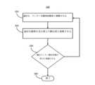
いくつかの実施形態では、循環堆積プロセスを利用して、酸化ハフニウムランタン膜を堆積させ得、そのような循環堆積プロセスの非限定的な例は、図1~3を参照して理解され得、図1は、循環堆積スーパーサイクルを含む例示的な循環堆積プロセス全体を示し、図2は、酸化ハフニウム膜を堆積するための例示的な第1のサブサイクルを示し、図3は、酸化ランタン膜を堆積させるための例示的な第2のサブサイクルを示す。In some embodiments, a cyclic deposition process may be utilized to deposit a hafnium lanthanum oxide film, non-limiting examples of such cyclic deposition processes may be understood with reference to Figures 1-3, where Figure 1 illustrates an exemplary overall cyclic deposition process including a cyclic deposition supercycle, Figure 2 illustrates an exemplary first subcycle for depositing a hafnium oxide film, and Figure 3 illustrates an exemplary second subcycle for depositing a lanthanum oxide film.
より詳細には、図1は、HfLaOx膜の堆積に利用される第1のサブサイクル120および第2のサブサイクル130を含む循環堆積スーパーサイクル150を含む例示的な全体的循環堆積プロセス100を示す。より詳細には、循環堆積プロセス100は、基材を反応チャンバー内に供給することと、基材を所望の堆積温度に加熱することと、を含むプロセス110によって開始することができる。 1 illustrates an exemplary overall
本開示のいくつかの実施形態では、基材は、高いアスペクト比形体、例えば、トレンチ構造および/またはフィン構造を含む平面基材またはパターン付き基材を含むことができる。基材は、シリコン(Si)、ゲルマニウム(Ge)、ゲルマニウムスズ(GeSn)、シリコンゲルマニウム(SiGe)、シリコンゲルマニウムスズ(SiGeSn)、炭化シリコン(SiC)、またはIII‐V族半導体材料、例えば、ガリウムヒ素(GaAs)、ガリウムリン(GaP)、もしくは窒化ガリウム(GaN)を含む1つ以上の材料を含むことができるが、これらに限定されない。本開示のいくつかの実施形態では、基材は設計された基材を備え得、表面半導体層は、その間に配置された介在する埋め込み酸化(BOX)によってバルク支持体上に配置される。In some embodiments of the present disclosure, the substrate may include a planar substrate or a patterned substrate including high aspect ratio features, such as trench and/or fin structures. The substrate may include one or more materials including, but not limited to, silicon (Si), germanium (Ge), germanium tin (GeSn), silicon germanium (SiGe), silicon germanium tin (SiGeSn), silicon carbide (SiC), or a III-V semiconductor material, such as gallium arsenide (GaAs), gallium phosphide (GaP), or gallium nitride (GaN). In some embodiments of the present disclosure, the substrate may comprise an engineered substrate, where a surface semiconductor layer is disposed on a bulk support with an intervening buried oxide (BOX) disposed therebetween.
パターン形成された基材は、基材の表面内または表面上に形成された半導体デバイス構造を含むことができる基材を備えることができ、例えば、パターン形成された基材は、部分的に製造された半導体デバイス構造、例えばトランジスタおよび/またはメモリ素子を含むことができる。いくつかの実施形態では、基材は、単結晶表面および/または、多結晶表面および/または非結晶表面などの非単結晶表面を含み得る1つ以上の二次表面を含み得る。単結晶表面は、例えば、シリコン(Si)、シリコンゲルマニウム(SiGe)、ゲルマニウムスズ(GeSn)、またはゲルマニウム(Ge)のうちの1つ以上を含み得る。多結晶または非結晶表面は、誘電体材料、例えば酸化物、酸窒化物または窒化物、例えば酸化ケイ素および窒化ケイ素などを含むことができる。The patterned substrate may comprise a substrate that may include semiconductor device structures formed in or on the surface of the substrate, for example, the patterned substrate may include partially fabricated semiconductor device structures, such as transistors and/or memory elements. In some embodiments, the substrate may include one or more secondary surfaces that may include single crystal surfaces and/or non-single crystal surfaces, such as polycrystalline surfaces and/or amorphous surfaces. The single crystal surfaces may include, for example, one or more of silicon (Si), silicon germanium (SiGe), germanium tin (GeSn), or germanium (Ge). The polycrystalline or amorphous surfaces may include dielectric materials, such as oxides, oxynitrides, or nitrides, such as silicon oxide and silicon nitride.
堆積に利用される反応チャンバーは、原子層堆積反応チャンバー、または化学蒸着反応チャンバー、または本明細書で前述したような反応チャンバーのいずれかであってもよい。本開示のいくつかの実施形態では、基材は、循環堆積プロセスの間、所望の堆積温度に加熱され得る。例えば、基材は、約750℃未満、または約650℃未満、または約550℃未満、または約450℃未満、または約350℃未満、または約300℃未満、または約250℃未満、または約150℃未満の基材温度まで加熱され得る。本開示のいくつかの実施形態において、循環堆積プロセス中の基材温度は、100℃~400℃、または150℃~350℃、もしくは200℃~300℃であり得る。The reaction chamber utilized for deposition may be an atomic layer deposition reaction chamber, or a chemical vapor deposition reaction chamber, or any of the reaction chambers as previously described herein. In some embodiments of the present disclosure, the substrate may be heated to a desired deposition temperature during the cyclical deposition process. For example, the substrate may be heated to a substrate temperature of less than about 750° C., or less than about 650° C., or less than about 550° C., or less than about 450° C., or less than about 350° C., or less than about 300° C., or less than about 250° C., or less than about 150° C. In some embodiments of the present disclosure, the substrate temperature during the cyclical deposition process may be from 100° C. to 400° C., or from 150° C. to 350° C., or from 200° C. to 300° C.
基材を所望の堆積温度に加熱すると、図1の例示的な循環堆積プロセス100は、循環堆積スーパーサイクル150を継続することができ、これは、第1のサブサイクルの少なくとも1回の堆積サイクルを利用して酸化ハフニウム膜を堆積させることと、第2のサブサイクルの少なくとも1回の堆積サイクルを利用して酸化ランタン膜を堆積させることとのうちの1回以上の繰り返しを含む。循環堆積スーパーサイクル150は、第1のサブサイクルの少なくとも1回の堆積サイクルを利用して、酸化ハフニウム膜を堆積させることを含む、プロセスブロック120によって開始され得る。Upon heating the substrate to a desired deposition temperature, the exemplary
図2は、第1のサブサイクル120およびその構成サブプロセスをより詳細に図示する。例えば、第1のサブサイクル120は、基材をハフニウム気相反応物(「ハフニウム前駆体」)と接触または曝すことを含むサブプロセスブロック210によって開始され得る。Figure 2 illustrates the
いくつかの実施形態では、ハフニウム前駆体は、ハロゲン化ハフニウム前駆体、ハフニウム有機金属前駆体、または有機金属ハフニウム前駆体のうちの少なくとも1つを含んでもよい。In some embodiments, the hafnium precursor may include at least one of a hafnium halide precursor, a hafnium organometallic precursor, or an organometallic hafnium precursor.
本明細書において後述するように、いくつかの実施形態では、ハロゲン化ハフニウム前駆体は少なくとも1つのハロゲン配位子を含んでもよく、一方残りの配位子、例えば金属有機または有機金属配位子は異なる。いくつかの実施形態では、ハロゲン化ハフニウム前駆体は、1つ、2つ、3つまたは4つのハロゲン化物配位子、例えば塩化物配位子を含んでもよい。As described later in this specification, in some embodiments, the hafnium halide precursor may include at least one halogen ligand, while the remaining ligands, e.g., metallo-organic or organometallic ligands, are different. In some embodiments, the hafnium halide precursor may include one, two, three, or four halide ligands, e.g., chloride ligands.
いくつかの実施形態では、ハロゲン化ハフニウム前駆体は、塩化ハフニウム、ヨウ化ハフニウム、または臭化ハフニウムのうちの少なくとも1つを含んでもよい。いくつかの実施形態では、塩化ハフニウムは四塩化ハフニウム(HfCl4)を含んでもよい。いくつかの実施形態では、ヨウ化ハフニウムは、四ヨウ化ハフニウム(HfI4)を含んでもよい。いくつかの実施形態では、臭化ハフニウムは、四臭化ハフニウム(HfBr4)を含んでもよい。 In some embodiments, the hafnium halide precursor may include at least one of hafnium chloride, hafnium iodide, or hafnium bromide. In some embodiments, the hafnium chloride may include hafnium tetrachloride (HfCl4 ). In some embodiments, the hafnium iodide may include hafnium tetraiodide (HfI4 ). In some embodiments, the hafnium bromide may include hafnium tetrabromide (HfBr 4) .
いくつかの実施形態では、ハフニウム有機金属前駆体は、ハフニウムアルキルアミド前駆体、ハフニウムシクロペンタジエニル配位子含有前駆体、または他の有機金属ハフニウム前駆体のうちの少なくとも1つを含むことができる。In some embodiments, the hafnium organometallic precursor can include at least one of a hafnium alkylamide precursor, a hafnium cyclopentadienyl ligand-containing precursor, or other organometallic hafnium precursor.
いくつかの実施形態では、ハフニウムアルキルアミド前駆体は、テトラキス(エチルメチルアミド)ハフニウム(Hf(NEtMe)4)、テトラキス(ジメチルアミド)ハフニウム(Hf(NMe2)4)、またはテトラキス(ジエチルアミド)ハフニウム(Hf(NEt2)4)を含む群から選択されてもよい。 In some embodiments, the hafnium alkylamide precursor may be selected from the group including tetrakis(ethylmethylamido)hafnium (Hf(NEtMe)4 ), tetrakis(dimethylamido)hafnium (Hf(NMe2 )4 ), or tetrakis(diethylamido)hafnium (Hf(NEt2 )4 ).
本開示のいくつかの実施形態では、ハフニウムシクロペンタジエニル配位子含有前駆体は、トリス(アルキルアミド)シクロペンタジエニルハフニウム、例えばトリス(ジメチルアミド)シクロペンタジエニルハフニウム(HfCp(NMe2)3)、またはビス(メチルシクロペンタジエニル)メトキシメチルハフニウム((MeCp)2Hf(CH)3(OCH3))またはそれらの誘導体、例えば、それらの前駆体のシクロペンタジエニル配位子に結合したアルキルなどの1つ以上の炭化水素、またはアルキルアミド配位子の他のアルキル基があるものなどを含む群から選択され得る。 In some embodiments of the present disclosure, the hafnium cyclopentadienyl ligand-containing precursor may be selected from the group including tris(alkylamido)cyclopentadienylhafnium, such astris(dimethylamido)cyclopentadienylhafnium (HfCp(NMe2)3), or bis(methylcyclopentadienyl)methoxymethylhafnium((MeCp)2Hf(CH)3(OCH3)) or derivatives thereof, such as those having one or more hydrocarbon groups, such as alkyl or other alkyl groups of the alkylamido ligands attached to the cyclopentadienyl ligands of the precursors.
いくつかの実施形態では、ハフニウム前駆体は、次式を有し:
HfL1L2L3L4
式中、L1~L4までのL配位子の各々は、
a)ハロゲン化物、例えば塩化物、臭化物、またはヨウ化物、
b)アルキルアミド、例えばジメチルアミド(‐NMe2)、ジエチルアミド(‐NEt2)、エチルメチルアミド(‐NEtMe)、
c)アミジネート、例えばN,N’‐ジメチルホルムアミジネート、
d)グアニジネート、例えばN,N’‐ジイソプロピル‐2‐エチルメチルアミドグアニジネート、
e)シクロペンタジエニルまたはそれらの誘導体、例えばシクロペンタジエニルもしくはメチルシクロペンタジエニルまたは他のアルキル置換シクロペンタジエニル配位子、
f)シクロヘプタジエニルまたはシクロヘプタトリエニル系、例えばシクロヘプタトリエニルまたはシクロヘプタジエニル
g)アルキル、例えばC1~C5アルキル、例えばヘテロレプティック前駆体の場合はほとんどがメチル、
h)アルコキシド、例えばメトキシド(‐OMe)、エトキシド(‐OEt)、イソプロポキシド(‐OiPr)、n‐ブトキシド(‐OBu)またはtert‐ブトキシド(‐OtBu)
i)ベータジケトネート、例えば(2,2,6,6‐テトラメチル‐3,5‐ヘプタンジオナト)(thd)、および/または
j)ドナー官能化アルコキシド、例えばジメチルエタノールアミン、であるように独立して選択され得る。 In some embodiments, the hafnium precursor has the formula:
HfL1 L2 L3 L4
wherein each of the L ligands L1 to L4 is
a) a halide, such as chloride, bromide, or iodide;
b) alkylamides, such as dimethylamide (-NMe2), diethylamide (-NEt2), ethylmethylamide (-NEtMe);
c) amidinates, such as N,N'-dimethylformamidinate;
d) guanidinates, such as N,N'-diisopropyl-2-ethylmethylamidoguanidinate;
e) cyclopentadienyl or derivatives thereof, such as cyclopentadienyl or methylcyclopentadienyl or other alkyl substituted cyclopentadienyl ligands;
f) cycloheptadienyl or cycloheptatrienyl systems, such as cycloheptatrienyl or cycloheptadienyl; g) alkyl, such as C1-C5 alkyl, e.g. mostly methyl in the case of heteroleptic precursors;
h) alkoxides, such as methoxide (-OMe), ethoxide (-OEt), isopropoxide (-OiPr ), n-butoxide (-OBu) or tert-butoxide (-OtBu ).
i) a beta-diketonate, such as (2,2,6,6-tetramethyl-3,5-heptanedionato) (thd), and/or j) a donor-functionalized alkoxide, such as dimethylethanolamine.
本開示のいくつかの実施形態では、ハフニウム前駆体は、窒素および/または酸素原子を介してHfに結合している1つ以上の二座配位子を含む。いくつかの実施形態では、ハフニウム前駆体は、窒素、酸素、および/または炭素を介してHfに結合している1つ以上の配位子を含む。In some embodiments of the present disclosure, the hafnium precursor includes one or more bidentate ligands bonded to Hf through nitrogen and/or oxygen atoms. In some embodiments, the hafnium precursor includes one or more ligands bonded to Hf through nitrogen, oxygen, and/or carbon.
本開示のいくつかの実施形態では、ハフニウム前駆体は、プラズマ励起前駆体を含まない、すなわち、酸化ハフニウム膜は、前駆体のプラズマ励起なしで堆積され、言い換えると、酸化ハフニウム膜は、プラズマのない環境で堆積される。In some embodiments of the present disclosure, the hafnium precursor does not include a plasma-excited precursor, i.e., the hafnium oxide film is deposited without plasma excitation of the precursor, in other words, the hafnium oxide film is deposited in a plasma-free environment.
本開示のいくつかの実施形態では、基材をハフニウム気相前駆体と接触させることは、ハフニウム前駆体を反応チャンバーにパルス注入することと、続いて、ハフニウム前駆体を基材に約0.01秒~約60秒、または約0.05秒~約10秒、または約0.1秒~約5.0秒の時間接触させることと、を含み得る。加えて、ハフニウム前駆体のパルス注入の間、ハフニウム前駆体の流量は、2000sccm未満、または500sccm未満、またはさらに100sccm未満とすることができる。加えて、基材上にハフニウム前駆体をパルス注入する間、ハフニウム前駆体の流量は、約1~2000sccm、または約5~1000sccm、または約10~約500sccmの範囲とすることができる。In some embodiments of the present disclosure, contacting the substrate with a hafnium vapor-phase precursor may include pulsing the hafnium precursor into the reaction chamber, followed by contacting the hafnium precursor with the substrate for a time period of about 0.01 seconds to about 60 seconds, or about 0.05 seconds to about 10 seconds, or about 0.1 seconds to about 5.0 seconds. In addition, during the pulsing of the hafnium precursor, the flow rate of the hafnium precursor may be less than 2000 sccm, or less than 500 sccm, or even less than 100 sccm. In addition, during the pulsing of the hafnium precursor onto the substrate, the flow rate of the hafnium precursor may range from about 1 to 2000 sccm, or from about 5 to 1000 sccm, or from about 10 to about 500 sccm.
図2の例示的なサブサイクル120は、反応チャンバーをパージすることによって継続することができる。例えば、過剰なレニウム前駆体および反応副生成物を(もしあれば)、例えば、不活性ガスで排出することにより、基材の表面から除去することができる。本開示のいくつかの実施形態では、パージプロセスは、パージサイクルを含んでもよく、基材表面は、約5.0秒未満、または約3.0秒未満、またはさらに約2.0秒未満の時間にわたってパージされる。過剰なハフニウム気相反応物、および任意の可能性のある反応副生成物を、反応チャンバーと流体連通するポンプシステムによって生成される真空を用いて除去してもよい。The
反応チャンバーをパージサイクルでパージすると、例示的な循環堆積サブサイクル120は、基材を第1の酸化剤前駆体と接触させるかまたは曝すことと、特に水(H2O)を含む第1の酸化剤前駆体と接触させることと、を含むサブプロセスブロック220により継続し得る。代替的な実施形態では、第1の酸化剤前駆体は、過酸化水素(H2O2)、オゾン(O3)、または窒素酸化物、例えば一酸化窒素(NO)、亜酸化窒素(N2O)、または二酸化窒素(NO2)のうちの少なくとも1つを含む。本開示のいくつかの実施形態では、酸化剤前駆体は、有機アルコール、例えばイソプロピルアルコールを含むことができる。 Upon purging the reaction chamber with the purge cycle, the exemplary
本開示のいくつかの実施形態では、第1の酸化剤前駆体は、プラズマ励起前駆体を含まない、すなわち、酸化ハフニウム膜は、前駆体のプラズマ励起なしで堆積される。言い換えれば、特定の実施形態では、酸化ハフニウム膜は、プラズマのない環境で堆積される。In some embodiments of the present disclosure, the first oxidizer precursor does not include a plasma-excited precursor, i.e., the hafnium oxide film is deposited without plasma excitation of the precursor. In other words, in certain embodiments, the hafnium oxide film is deposited in a plasma-free environment.
本開示のいくつかの実施形態では、基材を第1の酸化剤前駆体と接触させることは、第1の酸化剤前駆体、例えば水(H2O)を反応チャンバーにパルス注入することと、続いて、基材を第1の酸化剤前駆体に約0.01秒~約60秒、または約0.05秒~約10秒、または約0.1秒~約5.0秒の時間接触させることと、を含み得る。加えて、第1の酸化剤前駆体のパルス注入の間、第1の酸化剤前駆体の流量は、2000sccm未満、または500sccm未満、またはさらに100sccm未満とすることができる。加えて、基材上に第1の酸化剤前駆体をパルス注入する間、第1の酸化剤前駆体の流量は、約1~2000sccm、または約5~1000sccm、または約10~約500sccmの範囲とすることができる。 In some embodiments of the present disclosure, contacting the substrate with the first oxidizer precursor may include pulsing the first oxidizer precursor, such as water (H2 O), into the reaction chamber, followed by contacting the substrate with the first oxidizer precursor for a time period of about 0.01 seconds to about 60 seconds, or about 0.05 seconds to about 10 seconds, or about 0.1 seconds to about 5.0 seconds. Additionally, during the pulsing of the first oxidizer precursor, the flow rate of the first oxidizer precursor may be less than 2000 sccm, or less than 500 sccm, or even less than 100 sccm. Additionally, during the pulsing of the first oxidizer precursor onto the substrate, the flow rate of the first oxidizer precursor may range from about 1 to 2000 sccm, or from about 5 to 1000 sccm, or from about 10 to about 500 sccm.
第1の酸化剤前駆体が水(H2O)を含む実施形態では、水の純度は、その電気抵抗率によって特徴付けられてもよく、例えば、水の電気抵抗率が高いほど純度が高くなり、したがって不要な堆積膜中の汚染物質を減少させ得る。いくつかの実施形態では、第1酸化剤前駆体は、5MΩ・cmを超える、または10MΩ・cmを超える、または15MΩ・cmを超える、または20MΩ・cmを超える電気抵抗率を有する水(H2O)を含むことができる。本開示のいくつかの実施形態では、酸化ハフニウム膜の堆積で利用される水の電気抵抗率は、5MΩ・cm~20MΩ・cmであってもよい。 In embodiments where the first oxidizer precursor comprises water (H2 O), the purity of the water may be characterized by its electrical resistivity, for example, a higher electrical resistivity of water may indicate higher purity and therefore reduce unwanted contaminants in the deposited film. In some embodiments, the first oxidizer precursor may comprise water (H2 O) having an electrical resistivity of greater than 5 MΩ·cm, or greater than 10 MΩ·cm, or greater than 15 MΩ·cm, or greater than 20 MΩ·cm. In some embodiments of the present disclosure, the electrical resistivity of water utilized in the deposition of the hafnium oxide film may be between 5 MΩ·cm and 20 MΩ·cm.
図2の例示的なサブサイクル120は、反応チャンバーをパージすることによって継続することができる。例えば、過剰な第1の酸化剤前駆体および反応副生成物を(もしあれば)、例えば、不活性ガスで排出することにより、基材の表面から除去することができる。本開示のいくつかの実施形態では、パージプロセスは、パージサイクルを含んでもよく、基材表面は、約5.0秒未満、または約3.0秒未満、またはさらに約2.0秒未満の時間にわたってパージされる。過剰な1の酸化剤前駆体、例えば水および可能性のある反応副生成物を、反応チャンバーと流体連通するポンプシステムによって生成される真空を用いて除去してもよい。The
図2のサブサイクル120は、決定ゲートを含むサブプロセスブロック230によって継続されてもよく、決定ゲートは、例示的な第1のサブサイクル120によって堆積される酸化ハフニウム膜の厚さに依存する。酸化ハフニウム膜がその後のプロセス工程に対して不十分な厚さである場合、循環サブサイクル120は、サブプロセスブロック210に戻り、基材を、ハフニウム気相前駆体と接触させ(サブプロセスブロック210)、第1の酸化剤前駆体と接触させてもよい(サブプロセスブロック220)。例えば、第1のサブサイクル120の単一堆積サイクル、すなわち単位堆積サイクルは、基材をハフニウム前駆体と接触させることと、反応チャンバーをパージすることと、基材を水と接触させることと、反応チャンバーを再びパージすることと、を含み得る。酸化ハフニウム膜を所望の厚さに堆積させるために、サブサイクル120は、酸化ハフニウム膜の所望の厚さが堆積するまで1回以上繰り返されてもよく、その時点で、例示的な第1のサブサイクルをサブプロセスブロック240を介して終了してもよい。2 may be continued by
本開示の一部の実施形態では、基材のハフニウム前駆体および第1の酸化剤前駆体との接触順序は、基材が最初に第1の酸化剤前駆体と接触してその後ハフニウム前駆体と接触するようにし得ることは理解されたい。加えて、いくつかの実施形態では、循環堆積サブサイクル120は、基材を第1の酸化剤前駆体と1回以上接触させる前に、基材をハフニウム前駆体と1回以上接触させることを含むことができる。加えて、いくつかの実施形態では、循環堆積サブサイクル120は、基材をハフニウム前駆体と1回以上接触させる前に、基材を第1の酸化剤前駆体と1回以上接触させることを含むことができる。It should be appreciated that in some embodiments of the present disclosure, the order of contacting the substrate with the hafnium precursor and the first oxidizer precursor may be such that the substrate is first contacted with the first oxidizer precursor and then with the hafnium precursor. Additionally, in some embodiments, the
本開示のいくつかの実施形態では、例示的な循環第1のサブサイクル120は、基材をハフニウム前駆体および第1の酸化剤前駆体と交互に接触させ、ハフニウム前駆体と第1の酸化剤前駆体、例えば水との反応により基材の表面上に酸化ハフニウム膜を堆積させ得る。In some embodiments of the present disclosure, an exemplary cyclic
本開示のいくつかの実施形態では、例示的な循環堆積サブサイクル120を繰り返すことはできず、単位サイクル、すなわち堆積プロセスのうちの1つの堆積サイクルのみを実行することができる。例えば、基材をハフニウム前駆体と接触させ、続いて第1の酸化剤前駆体と接触させて、酸化ハフニウム膜の単一単層または単一単層未満を堆積させることができ、すなわち、いくつかの実施形態では、酸化ハフニウム膜は、単一の単層または単一の単層未満を含む。酸化ハフニウム膜の堆積に1つの堆積サイクルが利用されるこのような実施形態では、酸化ハフニウム膜は、5オングストローム未満、または2オングストローム未満、またはさらに1オングストローム未満の厚さを有し得る。いくつかの実施形態では、酸化ハフニウム膜は、連続膜を含まないが、基材上に配置された酸化ハフニウムの複数の分離領域を含むことができる。In some embodiments of the present disclosure, the exemplary
本開示のいくつかの実施形態では、例示的な循環堆積サブサイクル120を1回以上繰り返して、酸化ハフニウム膜を所望の厚さに堆積させることができる。本開示のいくつかの実施形態では、第1のサブサイクル120の単位堆積サイクルは、基材をハフニウム前駆体と接触させることと、反応チャンバーをパージすることと、基材を第1の酸化剤前駆体と接触させることと、再び反応チャンバーをパージすることと、を含み得る。本開示のいくつかの実施形態では、サブサイクル120の単位堆積サイクルは、2回を超えて、または4回を超えて、または6回を超えて、または8回を超えて、または10回を超えて、または15回を超えて、または20回を超えて実行され得る。いくつかの実施形態では、単位堆積サイクルを繰り返して、酸化ハフニウム膜を3ナノメートル未満、または2ナノメートル未満、または1ナノメートル未満、または5オングストローム未満、またはさらに2オングストローム未満の厚さまで堆積し得る。いくつかの実施形態では、酸化ハフニウム膜は、連続膜を含まないが、むしろ基材上に配置された酸化ハフニウムの複数の分離領域を含むことができる。 In some embodiments of the present disclosure, the exemplary
プロセスブロック120、すなわち、第1のサブサイクルが完了すると、循環堆積スーパーサイクル150(図1)は、第2のサブサイクルの少なくとも1回の堆積サイクルを利用して、酸化ランタン膜を堆積させることを含むプロセスブロック130によって継続され得る。Upon completion of
図3は、第2のサブサイクル130およびその構成サブプロセスをより詳細に示し、第2のサブサイクル130は、基材をランタン気相前駆体(「ランタン前駆体」)と接触または曝すことを含むサブプロセスブロック310によって開始し得る。Figure 3 illustrates the
本開示のいくつかの実施形態では、ランタン前駆体は、例えば、ランタンホルムアミジネート(La(FAMD)3)、またはトリス(N,N’‐ジイソプロピルアセトアミナト)ランタン(La(iPrAMD)3)などのアミジネート系前駆体を含み得る。いくつかの実施形態では、ランタン前駆体は、例えば(La(THD)3)などのジケトネート前駆体を含み得る。いくつかのの実施形態では、ランタン前駆体は、例えばトリス(イソプロピル‐シクロペンタジエニル)ランタン(La(iPrCp)3)などのCp(シクロペンタジエニル)ベースの前駆体を含み得る。いくつかの実施形態では、ランタン前駆体は、例えば、トリス(ビストリメチルシリルアミド)ランタン(La[N(SiMe3)2]3)などのアミドベースの化学物質を含み得る。 In some embodiments of the present disclosure, the lanthanum precursor may include an amidinate-based precursor, such as, for example, lanthanum formamidinate (La(FAMD)3 ), or tris(N,N'-diisopropylacetaminato)lanthanum (La(iPrAMD)3). In some embodiments, the lanthanum precursor may include a diketonate precursor, such as, for example, (La(THD)3 ). In some embodiments, the lanthanum precursor may include a Cp (cyclopentadienyl)-based precursor, such as, for example, tris(isopropyl-cyclopentadienyl)lanthanum (La(iPrCp)3 ). In some embodiments, the lanthanum precursor may include an amide-based chemistry, such as, for example, tris(bistrimethylsilylamido)lanthanum (La[N(SiMe3 )2 ]3 ).
いくつかの実施形態では、ランタン前駆体は、上記のハイブリッド的組み合わせを含み得る。他の実施形態では、ランタン前駆体は、例えばランタンアミジネートなどの窒素間の結合を有するランタン前駆体を含み得る。アミジネート化合物は、窒素とランタンとの間の結合をもたらす非局在化電子を含み得る。他の実施形態では、ランタン前駆体は、例えばランタンシクロペンタジエニルなどの炭素の結合を有するランタン前駆体を含み得る。このような実施形態では、ランタン前駆体は、炭素とランタンの間の結合が形成される化合物であると考えられる非局在化電子を含み得る。他の実施形態では、ランタン前駆体は、例えばランタンアミジネートおよびランタンシクロペンタジエニルなどの窒素と炭素両方の結合を有するランタン前駆体を含み得る。In some embodiments, the lanthanum precursor may include a hybrid combination of the above. In other embodiments, the lanthanum precursor may include a lanthanum precursor having nitrogen-nitrogen bonds, such as, for example, lanthanum amidinate. The amidinate compound may include delocalized electrons resulting in a bond between nitrogen and lanthanum. In other embodiments, the lanthanum precursor may include a lanthanum precursor having carbon bonds, such as, for example, lanthanum cyclopentadienyl. In such embodiments, the lanthanum precursor may include delocalized electrons that are believed to be compounds in which a bond between carbon and lanthanum is formed. In other embodiments, the lanthanum precursor may include a lanthanum precursor having both nitrogen and carbon bonds, such as, for example, lanthanum amidinate and lanthanum cyclopentadienyl.
本開示のいくつかの実施形態では、ランタン前駆体は、プラズマ励起前駆体を含まない、すなわち、酸化ランタン膜は、前駆体のプラズマ励起なしで堆積され得、言い換えると、酸化ランタン膜は、プラズマのない環境で堆積され得る。In some embodiments of the present disclosure, the lanthanum precursor does not include a plasma-excited precursor, i.e., the lanthanum oxide film may be deposited without plasma excitation of the precursor, in other words, the lanthanum oxide film may be deposited in a plasma-free environment.
いくつかの実施形態では、基材をランタン気相反応物と接触させることは、ランタン前駆体を反応チャンバーにパルス注入することと、続いて、ランタン前駆体を基材に約0.01秒~約60秒、または約0.05秒~約10秒、または約0.1秒~約5.0秒の時間接触させることと、を含み得る。加えて、反応チャンバーへのランタン前駆体のパルス注入の間、ランタン前駆体の流量は、2000sccm未満、または500sccm未満、またはさらに100sccm未満とすることができる。加えて、基材上にランタン前駆体をパルス注入する間、ランタン前駆体の流量は、約1~2000sccm、または約5~1000sccm、または約10~約500sccmの範囲とすることができる。In some embodiments, contacting the substrate with the lanthanum gas-phase reactant may include pulsing the lanthanum precursor into the reaction chamber, followed by contacting the lanthanum precursor with the substrate for a time period of about 0.01 seconds to about 60 seconds, or about 0.05 seconds to about 10 seconds, or about 0.1 seconds to about 5.0 seconds. Additionally, during the pulsing of the lanthanum precursor into the reaction chamber, the flow rate of the lanthanum precursor may be less than 2000 sccm, or less than 500 sccm, or even less than 100 sccm. Additionally, during the pulsing of the lanthanum precursor onto the substrate, the flow rate of the lanthanum precursor may range from about 1 to 2000 sccm, or from about 5 to 1000 sccm, or from about 10 to about 500 sccm.
図3の例示的なサブサイクル130は、反応チャンバーをパージすることによって継続することができる。例えば、過剰なランタン気相反応物および反応副生成物を(もしあれば)、例えば、不活性ガスで排出することにより、基材の表面から除去することができる。本開示のいくつかの実施形態では、パージプロセスは、パージサイクルを含んでもよく、基材表面は、約5.0秒未満、または約3.0秒未満、またはさらに約2.0秒未満の時間にわたってパージされる。過剰なランタン前駆体、および可能性のある反応副生成物を、反応チャンバーと流体連通するポンプシステムによって生成される真空を用いて除去してもよい。The
反応チャンバーをパージサイクルでパージすると、例示的な循環堆積サブサイクル130は、基材を第2の酸化剤前駆体、特に分子状酸素(O2)を含む第2の酸化剤前駆体と接触させるかまたは曝すこととを含むサブプロセスブロック320により継続し得る。代替的な実施形態では、第2の酸化剤前駆体は、水(H2O)、過酸化水素(H2O2)、オゾン(O3)、または窒素酸化物、例えば一酸化窒素(NO)、亜酸化窒素(N2O)、または二酸化窒素(NO2)を含み得る。本開示のいくつかの実施形態では、酸化剤前駆体は、有機アルコール、例えばイソプロピルアルコールを含むことができる。 Upon purging the reaction chamber with the purge cycle, the exemplary
本開示のいくつかの実施形態では、第2の酸化剤前駆体、例えば分子状酸素(O2)は、プラズマ励起前駆体を含まない、すなわち、酸化ランタン膜は、前駆体のプラズマ励起なしで堆積され、言い換えると、酸化ランタン膜は、プラズマのない環境で堆積される。 In some embodiments of the present disclosure, the second oxidant precursor, e.g., molecular oxygen (O2 ), does not include a plasma-excited precursor, i.e., the lanthanum oxide film is deposited without plasma excitation of the precursor, in other words, the lanthanum oxide film is deposited in a plasma-free environment.
第2の酸化剤前駆体が分子状酸素(O2)を含む実施形態では、分子状酸素(O2)の高純度供給源は、堆積した酸化ランタン膜の不要な汚染を実質的に防止するために利用されてもよい。したがって、いくつかの実施形態では、分子状酸素(O2)は、99.99%を超える、または99.999%を超える、または99.9999%を超える、または99.99999%を超える純度を有してもよい。 In embodiments where the second oxidant precursor comprises molecular oxygen (O2 ), a high purity source of molecular oxygen (O2 ) may be utilized to substantially prevent unwanted contamination of the deposited lanthanum oxide film. Thus, in some embodiments, the molecular oxygen (O2 ) may have a purity of greater than 99.99%, or greater than 99.999%, or greater than 99.9999%, or greater than 99.99999%.
本開示のいくつかの実施形態では、基材を第2の酸化剤前駆体、例えば分子状酸素(O2)と接触させることは、第2の酸化剤前駆体を反応チャンバーにパルス注入することと、続いて、基材を第2の酸化剤前駆体に約0.01秒~約60秒、または約0.05秒~約10秒、または約0.1秒~約5.0秒の時間接触させることと、を含み得る。加えて、反応チャンバーへの第2の酸化剤前駆体のパルス注入の間、第2の酸化剤前駆体の流量は、2000sccm未満、または500sccm未満、またはさらに100sccm未満とすることができる。加えて、基材上に第2の酸化剤前駆体をパルス注入する間、第2の酸化剤前駆体の流量は、約1~約2000sccm、または約5~約1000sccm、または約10~約500sccmの範囲とすることができる。 In some embodiments of the present disclosure, contacting the substrate with a second oxidizer precursor, such as molecular oxygen (O2 ), may include pulsing the second oxidizer precursor into the reaction chamber, followed by contacting the substrate with the second oxidizer precursor for a time period of about 0.01 seconds to about 60 seconds, or about 0.05 seconds to about 10 seconds, or about 0.1 seconds to about 5.0 seconds. Additionally, during the pulsing of the second oxidizer precursor into the reaction chamber, the flow rate of the second oxidizer precursor can be less than 2000 sccm, or less than 500 sccm, or even less than 100 sccm. Additionally, during the pulsing of the second oxidizer precursor onto the substrate, the flow rate of the second oxidizer precursor can range from about 1 to about 2000 sccm, or from about 5 to about 1000 sccm, or from about 10 to about 500 sccm.
図3の例示的なサブサイクル130は、反応チャンバーをパージすることによって継続することができる。例えば、過剰な第2の酸化剤前駆体および反応副生成物を(もしあれば)、例えば、不活性ガスで排出することにより、基材の表面から除去することができる。本開示のいくつかの実施形態では、パージプロセスは、パージサイクルを含んでもよく、基材表面は、約5.0秒未満、または約3.0秒未満、またはさらに約2.0秒未満の時間にわたってパージされる。過剰な第2の酸化剤前駆体および可能性のある反応副生成物を、反応チャンバーと流体連通するポンプシステムによって生成される真空を用いて除去してもよい。3 can continue by purging the reaction chamber. For example, excess second oxidizer precursor and reaction by-products (if any) can be removed from the surface of the substrate, for example, by venting with an inert gas. In some embodiments of the present disclosure, the purging process can include a purge cycle, where the substrate surface is purged for a time period less than about 5.0 seconds, or less than about 3.0 seconds, or even less than about 2.0 seconds. Excess second oxidizer precursor and possible reaction by-products can be removed using a vacuum generated by a pump system in fluid communication with the reaction chamber.
図3のサブサイクル130は、決定ゲートを含むサブプロセスブロック330によって継続されてもよく、決定ゲートは、例示的な第2のサブサイクル130によって堆積される酸化ランタン膜の厚さに依存する。酸化ランタン膜がその後のプロセス工程に対して不十分な厚さである場合、循環サブサイクル130は、サブプロセスブロック310に戻り、基材を、ランタン前駆体と接触させ(サブプロセスブロック310)、第2の酸化剤前駆体、例えば分子状酸素(O2)と接触させてもよい(サブプロセスブロック320)。例えば、第2のサブサイクル130の単一堆積サイクル、すなわち単位堆積サイクルは、基材をランタン気相前駆体と接触させることと、反応チャンバーをパージすることと、基材を第2の酸化剤前駆体と接触させることと、反応チャンバーを再びパージすることと、を含み得る。酸化ランタン膜を所望の厚さに堆積させるために、サブサイクル130は、酸化ランタン膜の所望の厚さが基材上に堆積するまで1回以上繰り返されてもよく、その時点で、例示的な第2のサブサイクル130をサブプロセスブロック340を介して終了してもよい。 3 may continue with
本開示の一部の実施形態では、基材のランタン前駆体および第2の酸化剤前駆体との接触順序は、基材が最初に第2の酸化剤前駆体と接触してその後ランタン前駆体と接触するようにし得ることは理解されたい。加えて、いくつかの実施形態では、循環堆積の第2のサブサイクル130は、基材を第2の酸化剤前駆体と1回以上接触させる前に、基材をランタン前駆体と1回以上接触させることを含むことができる。加えて、いくつかの実施形態では、循環堆積の第2のサブサイクル130は、基材をランタン前駆体と1回以上接触させる前に、基材を第2の酸化剤前駆体と1回以上接触させることを含むことができる。It should be understood that in some embodiments of the present disclosure, the order of contacting the substrate with the lanthanum precursor and the second oxidant precursor may be such that the substrate is first contacted with the second oxidant precursor and then with the lanthanum precursor. Additionally, in some embodiments, the
本開示のいくつかの実施形態では、例示的な循環サブサイクル130は、基材をランタン前駆体および第2の酸化剤前駆体と交互に接触させ、ランタン前駆体と第2の酸化剤前駆体との間の反応により基材上に酸化ランタン膜を堆積させ得る。In some embodiments of the present disclosure, the exemplary circulating
本開示のいくつかの実施形態では、例示的な循環堆積のサブサイクル130を繰り返すことはできず、単位サイクル、すなわち堆積プロセスのうちの1つの堆積サイクルのみを実行することができる。例えば、基材をランタン前駆体と接触させ、続いて第2の酸化剤前駆体と接触させて、酸化ランタン膜の単一単層または単一単層未満を堆積させることができ、すなわち、いくつかの実施形態では、酸化ランタン膜は、単一の単層または単一の単層未満を含む。酸化ランタン膜の堆積に1つの堆積サイクルが利用されるこのような実施形態では、酸化ランタン膜は、5オングストローム未満、または2オングストローム未満、またはさらに1オングストローム未満の厚さを有し得る。いくつかの実施形態では、酸化ランタン膜は、連続膜を含まないが、むしろ基材上に配置された酸化ランタンの複数の分離領域を含むことができる。In some embodiments of the present disclosure, the
本開示のいくつかの実施形態では、例示的な循環堆積サブサイクル130を1回以上繰り返して、酸化ランタン膜を所望の厚さに堆積させることができる。本開示のいくつかの実施形態では、第2のサブサイクル130の単位堆積サイクルは、基材をランタン前駆体と接触させることと、反応チャンバーをパージすることと、基材を第2の酸化剤前駆体と接触させることと、再び反応チャンバーをパージすることと、を含み得る。本開示のいくつかの実施形態では、サブサイクル130の単位堆積サイクルは、2回を超えて、または4回を超えて、または6回を超えて、または8回を超えて、または10回を超えて、または15回を超えて、または20回を超えて、またはさらに超えて実行され得る。いくつかの実施形態では、単位堆積サイクルを繰り返して、酸化ランタン膜を3ナノメートル未満、または2ナノメートル未満、または1ナノメートル未満、または5オングストローム未満、またはさらに2オングストローム未満の厚さまで堆積し得る。いくつかの実施形態では、酸化ランタン膜は、連続膜を含まないが、むしろ基材上に配置された酸化ランタンの複数の分離領域を含むことができる。 In some embodiments of the present disclosure, the exemplary
第2のサブサイクル130が完了すると、図1の例示的な循環堆積プロセス100は、決定ゲートを含むプロセスブロック140によって継続され得、決定ゲートは、第1のサブサイクルおよび第2のサブサイクルによって堆積された酸化ハフニウムランタン膜の合計厚さに依存する。酸化ハフニウムランタン膜の合計厚さが、所望の半導体デバイスの用途に不十分な場合、次に、循環堆積スーパーサイクル150は、プロセスブロック120に戻り、第1のサブサイクルの少なくとも1回の堆積サイクルを利用して酸化ハフニウム膜を堆積し、続いて、プロセスブロック130を利用して、第2のサブサイクルの少なくとも1回の堆積サイクルを利用して酸化ランタン膜を堆積させ、これにより、酸化ハフニウムと酸化ランタンの交互層を堆積させることにより繰り返すことができる。したがって、循環堆積スーパーサイクル150は、酸化ハフニウムランタン膜の所望の厚さが基材上に堆積されるまで1回以上繰り返されてもよい。酸化ハフニウムランタン膜の所望の厚さ達成されると、例示的な循環堆積プロセス100が、プロセスブロック160を介して終了し、その上に配置された酸化ハフニウムランタン膜を有する基材をさらなる半導体デバイス製作プロセスに供することができる。Upon completion of the
本開示のいくつかの実施形態では、基材上に酸化ハフニウム膜および酸化ランタン膜を堆積させる順序は、循環堆積スーパーサイクル150が最初に酸化ランタン膜を堆積し、続いて酸化ハフニウム膜を堆積し、その後必要に応じて酸化ランタン堆積および酸化ハフニウム堆積のステップを繰り返して酸化ハフニウムランタン膜の堆積をもたらすことを含むようにしてもよいことは理解されよう。It will be appreciated that in some embodiments of the present disclosure, the sequence of depositing hafnium oxide and lanthanum oxide films on a substrate may include a
本開示のいくつかの実施形態では、酸化ハフニウムランタン膜を堆積する方法は、酸化ハフニウム膜または成分(例えば、1つ以上の第1のサブサイクル)を堆積し、酸化ランタン膜または成分(例えば、1つ以上の第2のサブサイクル)を堆積する堆積プロセスの両方を含む。例えば、本開示に包含される酸化ハフニウムランタン膜を堆積させる方法は、1つ以上の酸化ハフニウム(HfOx)堆積サブサイクルおよび1つ以上の酸化ランタン(LaOx)堆積サブサイクルを含む多数のスーパーサイクル150を含み得る。 In some embodiments of the present disclosure, a method of depositing a hafnium lanthanum oxide film includes both a deposition process to deposit a hafnium oxide film or component (e.g., one or more first subcycles) and a deposition process to deposit a lanthanum oxide film or component (e.g., one or more second subcycles). For example, a method of depositing a hafnium lanthanum oxide film encompassed by the present disclosure may include
いくつかの実施形態では、堆積された酸化ハフニウムランタン膜の特定の特性は、個々のスーパーサイクル内で実行される第1のサブサイクル(HfOxサブサイクル)の数と実行される第2のサブサイクル(LaOxサブサイクル)の数の比を変えることによって制御され得る。言い換えれば、例示的な循環堆積プロセス100は、単位スーパーサイクル当たり実行される第2のサブサイクルに対する実行される第1のサブサイクルの比を含み得る。代替的に、例示的な循環堆積プロセス100は、単位スーパーサイクル当たり実行される第1のサブサイクルに対する実行される第2のサブサイクルの比を含み得る。いくつかの実施形態では、スーパーサイクル当たり実行される第1のサブサイクル(HfOxサブサイクル)に対する実行される第2のサブサイクル(LaOxサブサイクル)の比は、0.50未満、または0.40未満、または0.30未満、または0.20未満、または0.15未満、または0.10未満、またはさらに0.05未満である。 In some embodiments, the specific properties of the deposited hafnium lanthanum oxide film can be controlled by varying the ratio of the number of first subcycles (HfOx subcycles) performed to the number of second subcycles (LaOx subcycles) performed within each supercycle. In other words, the exemplary
いくつかの実施形態では、第1のサブサイクル(LaOxサブサイクル)の1つ以上の堆積パラメータは、所与のスーパーサイクル内または連続するスーパーサイクル間で別の第1のサブサイクル(LaOxサブサイクル)のそれと異なり得る。いくつかの実施形態では、第2のサブサイクル(HfOxサブサイクル)の1つ以上の堆積パラメータは、所与のスーパーサイクル内または連続するスーパーサイクル間で別の第2のサブサイクル(HfOxサブサイクル)のそれと異なり得る。いくつかの実施形態では、第1のサブサイクルまたは第2のサブサイクルの堆積パラメータは、堆積プロセス全体を通して、すなわち、1つ以上の連続するスーパーサイクルの上で実質的に同一であり得る。 In some embodiments, one or more deposition parameters of a first subcycle (LaOx subcycle) may be different from that of another first subcycle (LaOx subcycle) within a given supercycle or between successive supercycles. In some embodiments, one or more deposition parameters of a second subcycle (HfOx subcycle) may be different from that of another second subcycle (HfO xsubcycle ) within a given supercycle or between successive supercycles. In some embodiments, the deposition parameters of a first subcycle or a second subcycle may be substantially the same throughout the deposition process, i.e., over one or more successive supercycles.
本開示のいくつかの実施形態において、スーパーサイクル当たり実行される第1のサブサイクル(HfOxサブサイクル)に対する実行される第2のサブサイクル(LaOxサブサイクル)の比は、酸化ハフニウムランタン膜の組成、例えば、酸化ハフニウムランタン膜中のランタン組成(原子%)などを制御するために利用され得る。より詳細には、図4は、本開示の実施形態による酸化ランタン堆積サブサイクル対酸化ハフニウム堆積サブサイクルの比に関連するいくつかの例示的な酸化ハフニウムランタン膜のランタン組成(原子%)の変化を示すX線光電子分光法(XPS)データを示す。図4の検査は、例示的なHfLaOx膜内に存在するLaOx:HfOxサブサイクル比とランタン組成(原子%)との間の明確な関係を示している。例えば、LaOx:HfOxサブサイクル比が減少すると、例示的なHfLaOx膜内のランタン組成も減少する。したがって、本開示の実施形態は、堆積した酸化ハフニウムランタン膜の組成をしっかりと制御する方法を提供することができる。例えば、本開示の実施形態に従って堆積させた酸化ハフニウムランタン膜は、10原子%未満、または7原子%未満、または5原子%未満、または3原子%未満、または2原子%未満、またはさらに1原子%以下のランタン組成を有し得る。いくつかの実施形態では、本開示の実施形態に従って堆積させた酸化ハフニウムランタン膜中のランタン組成は、0.5原子%~3原子%、または1.0原子%~2.5原子%であり得る。 In some embodiments of the present disclosure, the ratio of the second subcycle (LaOx subcycle) performed to the first subcycle (HfOxsubcycle ) performed per supercycle can be utilized to control the composition of the hafnium lanthanum oxide film, such as the lanthanum composition (atomic %) in the hafnium lanthanum oxide film. More specifically, FIG. 4 shows X-ray photoelectron spectroscopy (XPS) data illustrating the change in lanthanum composition (atomic %) of several exemplary hafnium lanthanum oxide films associated with the ratio of lanthanum oxide deposition subcycles to hafnium oxide deposition subcycles according to embodiments of the present disclosure. Inspection of FIG. 4 shows a clear relationship between theLaOx :HfOx subcycle ratio and the lanthanum composition (atomic %) present in the exemplaryHfLaOx films. For example, as theLaOx :HfOx subcycle ratio decreases, the lanthanum composition in the exemplaryHfLaOx films also decreases. Thus, embodiments of the present disclosure can provide a method to tightly control the composition of the deposited hafnium lanthanum oxide film. For example, hafnium lanthanum oxide films deposited according to embodiments of the present disclosure may have a lanthanum composition of less than 10 atomic %, or less than 7 atomic %, or less than 5 atomic %, or less than 3 atomic %, or less than 2 atomic %, or even 1 atomic % or less. In some embodiments, the lanthanum composition in hafnium lanthanumoxide films deposited according to embodiments of the present disclosure may be between 0.5 atomic % and 3 atomic %, or between 1.0 atomic % and 2.5 atomic %.
本開示のいくつかの実施形態では、酸化ハフニウムランタン膜を低濃度の不純物で堆積させ得る。例えば、酸化ハフニウムランタン膜は、10原子%未満、または5原子%未満、または2原子%未満、または1原子%未満、または0.5原子%未満、またはさらに0.2原子%未満のランタン組成を有し得る。いくつかの実施形態では、酸化ハフニウム膜内の不純物は、炭素を含むが、これに限定されない。例えば、酸化ハフニウムランタン膜は、10原子%未満、または5原子%未満、または2原子%未満、または1原子%未満、または0.5原子%未満、またはさらに0.2原子%未満の炭素濃度を有し得る。In some embodiments of the present disclosure, the hafnium lanthanum oxide film may be deposited with a low concentration of impurities. For example, the hafnium lanthanum oxide film may have a lanthanum composition of less than 10 atomic %, or less than 5 atomic %, or less than 2 atomic %, or less than 1 atomic %, or less than 0.5 atomic %, or even less than 0.2 atomic %. In some embodiments, the impurities in the hafnium oxide film include, but are not limited to, carbon. For example, the hafnium lanthanum oxide film may have a carbon concentration of less than 10 atomic %, or less than 5 atomic %, or less than 2 atomic %, or less than 1 atomic %, or less than 0.5 atomic %, or even less than 0.2 atomic %.
いくつかの実施形態では、酸化ハフニウム堆積サブサイクルおよび酸化ランタン堆積サブサイクルの2つの異なる酸化剤前駆体を利用することによって有効化される堆積プロセスの吸湿性の減少により、本開示の方法は、酸化ハフニウムランタン膜をより大きな組成均一性で堆積し得る。本開示のいくつかの実施形態では、本開示の実施形態に従って堆積させた酸化ハフニウムランタン膜中のランタン組成の均一性は、2原子%(1シグマ)未満、または0.5原子%(1シグマ)未満、または0.2原子%(1シグマ)未満、または0.1原子%(1シグマ)未満であり得る。本開示のいくつかの実施形態では、本開示の実施形態に従って堆積させた酸化ハフニウムランタン膜中のランタン組成の均一性は、2原子%(1シグマ)~0.1原子%(1シグマ)の間であり得る。本明細書で開示される実施形態では、元素の原子濃度は、ラザフォード後方散乱(RBS)またはx線光電子分光法(XPS)を利用して決定されうる。In some embodiments, due to the reduced hygroscopicity of the deposition process enabled by utilizing two different oxidizer precursors for the hafnium oxide and lanthanum oxide deposition subcycles, the methods of the present disclosure may deposit hafnium lanthanum oxide films with greater compositional uniformity. In some embodiments of the present disclosure, the uniformity of lanthanum composition in hafnium lanthanum oxide films deposited according to embodiments of the present disclosure may be less than 2 atomic % (1 sigma), or less than 0.5 atomic % (1 sigma), or less than 0.2 atomic % (1 sigma), or less than 0.1 atomic % (1 sigma). In some embodiments of the present disclosure, the uniformity of lanthanum composition in hafnium lanthanum oxide films deposited according to embodiments of the present disclosure may be between 2 atomic % (1 sigma) and 0.1 atomic % (1 sigma). In embodiments disclosed herein, the atomic concentrations of elements may be determined using Rutherford backscattering (RBS) or x-ray photoelectron spectroscopy (XPS).
いくつかの実施形態では、本明細書に開示される方法に従って堆積させた酸化ハフニウムランタンは、ナノラミネート膜を含み得る。すなわち、いくつかの実施形態では、別の層および異なる層は、酸化ハフニウムランタン膜内で視認可能であり得る。例えば、酸化ハフニウムランタン膜は、酸化ハフニウムおよび酸化ランタンの交互層を含むナノラミネートを含み得る。In some embodiments, the hafnium lanthanum oxide deposited according to the methods disclosed herein may comprise a nanolaminate film. That is, in some embodiments, separate and distinct layers may be visible within the hafnium lanthanum oxide film. For example, the hafnium lanthanum oxide film may comprise a nanolaminate that includes alternating layers of hafnium oxide and lanthanum oxide.
いくつかの実施形態では本明細書に開示される方法に従って堆積させた酸化ハフニウムランタンは、ナノラミネート膜ではない。すなわち、いくつかの実施形態では、別の層および異なる層は、本開示の実施形態に従って堆積された酸化ハフニウムランタン膜内で視認可能であり得えない。例えば、一様または実質的に組成上均一な酸化ハフニウムランタン膜は、本明細書に開示される方法によって堆積され得る。いくつかの実施形態では、酸化ハフニウムランタン膜は、実質的に組成上均一な三級酸化ハフニウムランタン膜を含む。In some embodiments, the hafnium lanthanum oxide deposited according to the methods disclosed herein is not a nanolaminate film. That is, in some embodiments, separate and distinct layers may not be visible within the hafnium lanthanum oxide film deposited according to embodiments of the present disclosure. For example, a uniform or substantially compositionally uniform hafnium lanthanum oxide film may be deposited by the methods disclosed herein. In some embodiments, the hafnium lanthanum oxide film comprises a substantially compositionally uniform tertiary hafnium lanthanum oxide film.
より詳細には、本開示のいくつかの実施形態では、本明細書に記載の循環堆積プロセスによって堆積させた酸化ハフニウムランタン膜は、実質的に組成上均一な酸化ハフニウムランタン膜を含み得る。例えば、本明細書に記載の循環堆積プロセスは、酸化ハフニウム膜および酸化ランタン膜を交互に堆積させることができる(またはその逆)。しかしながら、いくつかの実施形態では、酸化ハフニウムおよび酸化ランタンの膜は、5オングストローム未満の厚さに堆積する可能性があるため、交互の層が相互拡散し、実質的に組成上均一な酸化ハフニウムランタン膜が得られ、すなわち、酸化ハフニウム領域と酸化ランタン領域の間には、酸化ハフニウムランタン膜の識別可能な区別は存在しない。More specifically, in some embodiments of the present disclosure, the hafnium lanthanum oxide film deposited by the cyclic deposition process described herein may include a substantially compositionally uniform hafnium lanthanum oxide film. For example, the cyclic deposition process described herein may deposit alternating hafnium oxide and lanthanum oxide films (or vice versa). However, in some embodiments, the hafnium oxide and lanthanum oxide films may be deposited to a thickness of less than 5 angstroms, such that the alternating layers interdiffuse to result in a substantially compositionally uniform hafnium lanthanum oxide film, i.e., there is no discernible distinction between the hafnium oxide and lanthanum oxide regions of the hafnium lanthanum oxide film.
いくつかの実施形態では本開示の酸化ハフニウムランタン膜は、20ナノメートル~0.5ナノメートル、または15ナノメートル~1ナノメートル、または10ナノメートル~1.5ナノメートルの厚さに堆積されてもよい。いくつかの実施形態では、本開示の酸化ハフニウムランタン膜は、20ナノメートル未満、または15ナノメートル未満、または10ナノメートル未満、または8ナノメートル未満、またはさらに5ナノメートル未満の厚さまで堆積し得る。In some embodiments, the hafnium lanthanum oxide films of the present disclosure may be deposited to a thickness of 20 nanometers to 0.5 nanometers, or 15 nanometers to 1 nanometer, or 10 nanometers to 1.5 nanometers. In some embodiments, the hafnium lanthanum oxide films of the present disclosure may be deposited to a thickness of less than 20 nanometers, or less than 15 nanometers, or less than 10 nanometers, or less than 8 nanometers, or even less than 5 nanometers.
いくつかの実施形態では、酸化ハフニウムランタン膜の成長速度は、約0.1Å/サイクル~約5Å/サイクル、また0.2Å/サイクル~3Å/サイクル、または0.3Å/サイクル~2.0Å/サイクルであってもよい。いくつかの実施形態では、酸化ハフニウムランタン膜の成長速度は、0.3Å/サイクルより大きい、または0.5Å/サイクルより大きい、または0.8Å/サイクルより大きい、または1.0Å/サイクルより大きい、または1.2Å/サイクルより大きい。いくつかの実施形態では、酸化ハフニウムランタン膜の成長速度は、1.5Å/サイクル未満、または1.0Å/サイクル未満、または0.5Å/サイクル未満、または0.3Å/サイクル未満、または0.2Å/サイクル未満である。本明細書で引用された成長速度は、HfOxおよびLaOxサブサイクルの両方の結合数に基づく、すなわち、サイクルは、HfOxまたはLaOxサブサイクルを意味する。 In some embodiments, the growth rate of the hafnium lanthanum oxide film may be from about 0.1 Å/cycle to about 5 Å/cycle, also from 0.2 Å/cycle to 3 Å/cycle, or from 0.3 Å/cycle to 2.0 Å/cycle. In some embodiments, the growth rate of the hafnium lanthanum oxide film is greater than 0.3 Å/cycle, or greater than 0.5 Å/cycle, or greater than 0.8 Å/cycle, or greater than 1.0 Å/cycle, or greater than 1.2 Å/cycle. In some embodiments, the growth rate of the hafnium lanthanum oxide film is less than 1.5 Å/cycle, or less than 1.0 Å/cycle, or less than 0.5 Å/cycle, or less than 0.3 Å/cycle, or less than 0.2 Å/cycle. The growth rates cited herein are based on the number of bonds in both the HfOx and LaOx subcycles, i.e., the cycles refer to either the HfOx or the LaOx subcycles.
本明細書に開示される循環堆積プロセスによって堆積させた酸化ハフニウムランタン膜は、連続膜であってもよい。いくつかの実施形態において、酸化ハフニウムランタン膜は、100ナノメートル未満、または60ナノメートル未満、または50ナノメートル未満、または40ナノメートル未満、または30ナノメートル未満、または20ナノメートル未満、または10ナノメートル未満、または5ナノメートル未満、または2ナノメートル未満、または1ナノメートル未満、さらには0.5ナノメートル未満の厚さで連続的であり得る。本明細書で言及される連続性は、物理的連続性または電気的連続性であることができる。本開示のいくつかの実施形態では、酸化ハフニウムランタン膜が物理的に連続的であってもよい厚さは、膜が電気的に連続的である厚さと同じでなくてもよく、その逆もまた同じである。The hafnium lanthanum oxide film deposited by the cyclic deposition process disclosed herein may be a continuous film. In some embodiments, the hafnium lanthanum oxide film may be continuous at a thickness of less than 100 nanometers, or less than 60 nanometers, or less than 50 nanometers, or less than 40 nanometers, or less than 30 nanometers, or less than 20 nanometers, or less than 10 nanometers, or less than 5 nanometers, or less than 2 nanometers, or less than 1 nanometer, or even less than 0.5 nanometers. The continuity referred to herein can be physical continuity or electrical continuity. In some embodiments of the present disclosure, the thickness at which the hafnium lanthanum oxide film may be physically continuous may not be the same as the thickness at which the film is electrically continuous, and vice versa.
本開示のいくつかの実施形態では、酸化ハフニウムランタン膜は、例えば三次元、非平面の基材などの、高いアスペクト比特徴を含む基材上に形成され得る。いくつかの実施形態では、酸化ハフニウムランタン膜は、10:1を超え、または20:1を超え、または30:1を超え、またはさらに50:1を超える1つ以上のトレンチ構造および/またはフィン構造を含む基材上に堆積されてもよい。酸化ハフニウムランタン膜が高いアスペクト比特徴を含む基材上に堆積されるこのような実施形態では、堆積膜のステップカバレッジは、およそ90%を超え、またはおよそ95%を超え、またはおよそ99%を超え、またはさらに100%に実質的に等しい場合がある。In some embodiments of the present disclosure, the hafnium lanthanum oxide film may be formed on a substrate including high aspect ratio features, such as, for example, a three-dimensional, non-planar substrate. In some embodiments, the hafnium lanthanum oxide film may be deposited on a substrate including one or more trench and/or fin structures with a ratio of greater than 10:1, or greater than 20:1, or greater than 30:1, or even greater than 50:1. In such embodiments in which the hafnium lanthanum oxide film is deposited on a substrate including high aspect ratio features, the step coverage of the deposited film may be greater than approximately 90%, or greater than approximately 95%, or greater than approximately 99%, or even substantially equal to 100%.
本開示のいくつかの実施形態では、本開示の実施形態に従って堆積させた酸化ハフニウムランタン膜を1つ以上の堆積プロセスに供し、例えば、結晶性を改善するため、または膜を濃縮するために、膜の品質をさらに改善することができる。したがって、いくつかの実施形態では、本開示の方法は、酸化ハフニウムランタン膜を堆積後に熱アニールすることをさらに含み得る。例えば、酸化ハフニウムランタン膜は、800℃未満、または700℃未満、もしくは600℃未満、もしくは500℃未満、もしくは400℃未満、もしくはさらに300℃未満の温度で、または300℃~800℃、もしくは350℃~750℃、もしくは400℃~600℃の温度で熱アニールされ得る。In some embodiments of the present disclosure, the hafnium lanthanum oxide film deposited according to embodiments of the present disclosure can be subjected to one or more deposition processes to further improve the quality of the film, for example, to improve crystallinity or to concentrate the film. Thus, in some embodiments, the method of the present disclosure can further include thermally annealing the hafnium lanthanum oxide film after deposition. For example, the hafnium lanthanum oxide film can be thermally annealed at a temperature below 800°C, or below 700°C, or below 600°C, or below 500°C, or below 400°C, or even below 300°C, or at a temperature between 300°C and 800°C, or between 350°C and 750°C, or between 400°C and 600°C.
本開示のいくつかの実施形態では、酸化ハフニウムランタン膜の堆積後熱アニールを、制御された環境下で反応チャンバー内で実行され得る。例えば、酸化ハフニウムランタン膜の熱アニールは、例えば、希ガス(例えば、Ar、Heなど)または窒素などの不活性ガス雰囲気中で実施され得る。さらなる例において、酸化ハフニウムランタン膜の熱アニールは、例えばフォーミングガス(H2/N2)のような水素含有雰囲気で実行され得る。さらなる例において、酸化ハフニウムランタン膜の熱アニールは、例えば、分子状酸素(O2)、水(H2O)、オゾン(O3)、過酸化水素(H2O2)などの酸素含有雰囲気で実行され得る。 In some embodiments of the present disclosure, the post-deposition thermal annealing of the hafnium lanthanum oxide film may be performed in a reaction chamber under a controlled environment. For example, the thermal annealing of the hafnium lanthanum oxide film may be performed in an inert gas atmosphere, such as a noble gas (e.g., Ar, He, etc.) or nitrogen. In a further example, the thermal annealing of the hafnium lanthanum oxide film may be performed in a hydrogen-containing atmosphere, such as forming gas (H2 /N2 ). In a further example, the thermal annealing of the hafnium lanthanum oxide film may be performed in an oxygen-containing atmosphere, such as molecular oxygen (O2 ), water (H2O ), ozone (O3 ), hydrogen peroxide(H2O2) , etc.
本開示のいくつかの実施形態では、酸化ハフニウムランタン膜を熱アニールすることは、酸化ハフニウムランタン膜を少なくとも部分的に結晶化させることをさらに含む。いくつかの実施形態では、堆積後の酸化ハフニウムランタン膜を熱アニールすることは、主に斜方晶構造を含む酸化ハフニウムランタン膜を形成させ得る。いくつかの実施形態では、酸化ハフニウムランタン膜を熱アニールすることは、実質的に単結晶酸化ハフニウムランタン膜を形成させることをさらに含む。いくつかの実施形態では、実質的に単結晶酸化ハフニウムランタン膜は、主に斜方晶構造を含む。本開示のいくつかの実施形態では、酸化ハフニウムランタン膜をアモルファス状態で堆積させ得、酸化ハフニウムランタン膜を熱アニールすることは、LaHfOx膜の制御された結晶化を提供し得る。 In some embodiments of the present disclosure, thermally annealing the hafnium lanthanum oxide film further comprises at least partially crystallizing the hafnium lanthanum oxide film. In some embodiments, thermally annealing the deposited hafnium lanthanum oxide film may form a hafnium lanthanum oxide film comprising a predominantly orthorhombic crystal structure. In some embodiments, thermally annealing the hafnium lanthanum oxide film further comprises forming a substantially single crystalline hafnium lanthanum oxide film. In some embodiments, the substantially single crystalline hafnium lanthanum oxide film comprises a predominantly orthorhombic crystal structure. In some embodiments of the present disclosure, the hafnium lanthanum oxide film may be deposited in an amorphous state, and thermally annealing the hafnium lanthanum oxide film may provide controlled crystallization of the LaHfOx film.
図5は、様々な堆積温度およびランタン組成(原子%)を増加させた本開示の実施形態に従って堆積させた複数の例示的な酸化ハフニウムランタン膜の結晶化温度を示す例示的データを示す。図5の検査は、例示的な酸化ハフニウムランタン膜の結晶化温度が、例示的な酸化ハフニウムランタン膜のランタン組成(原子%)の減少とともに低下することを明らかにしている。非限定的な例として、酸化ハフニウムランタン膜は、600℃未満の結晶化温度を有する1原子%以下のランタンの組成を含んでもよい。はである。さらなる非限定的な例として、酸化ハフニウムランタン膜は、およそ450℃未満の結晶化温度を有する1原子以下のランタンの組成を含んでもよい。5 illustrates exemplary data showing the crystallization temperatures of several exemplary hafnium lanthanum oxide films deposited according to embodiments of the present disclosure at various deposition temperatures and increasing lanthanum composition (atomic %). Examination of FIG. 5 reveals that the crystallization temperature of the exemplary hafnium lanthanum oxide films decreases with decreasing lanthanum composition (atomic %) of the exemplary hafnium lanthanum oxide films. As a non-limiting example, the hafnium lanthanum oxide films may include a composition of 1 atomic % or less of lanthanum with a crystallization temperature less than 600° C. is. As a further non-limiting example, the hafnium lanthanum oxide films may include a composition of 1 atomic % or less of lanthanum with a crystallization temperature less than approximately 450° C.
図5の検査は、例示的な酸化ハフニウムランタン膜の結晶化温度が、酸化ハフニウムランタン膜の堆積温度の増加とともに低下することを明らかにしている。非限定的な例として、酸化ハフニウムランタン膜は、200°C未満の堆積温度で、かつ650℃未満、600℃未満、550℃未満、または550℃~650℃の温度で対応する結晶化温度で堆積された1原子%以下のランタンの組成を含んでもよい。さらなる非限定的な例として、酸化ハフニウムランタン膜は、300°C未満の堆積温度で、かつ550℃未満、または500℃未満、または450℃未満、または450℃~550℃の温度の対応する結晶化温度で堆積された1原子%以下の濃度のランタンを含んでもよい。Inspection of FIG. 5 reveals that the crystallization temperature of the exemplary hafnium lanthanum oxide film decreases with increasing deposition temperature of the hafnium lanthanum oxide film. As a non-limiting example, the hafnium lanthanum oxide film may include a composition of 1 atomic % or less of lanthanum deposited at a deposition temperature less than 200°C and a corresponding crystallization temperature at a temperature less than 650°C, less than 600°C, less than 550°C, or between 550°C and 650°C. As a further non-limiting example, the hafnium lanthanum oxide film may include a concentration of 1 atomic % or less of lanthanum deposited at a deposition temperature less than 300°C and a corresponding crystallization temperature less than 550°C, or less than 500°C, or less than 450°C, or between 450°C and 550°C.
図6は、様々な膜厚でランタン組成(原子%)が増加するいくつかの例示的な酸化ハフニウムランタンの結晶化温度を示す例示的なデータを示す。図6の検査は、前述のように、酸化ハフニウムランタン膜中のランタン含有量が減少するにつれて、結晶化温度が概ね減少することが明らかになる。さらなる図6の検査は、酸化ハフニウムランタン膜の厚さが増加するにつれて結晶化温度も低下することが明らかになる。例えば、いくつかの実施形態では、酸化ハフニウムランタン膜は、およそ540℃~680℃の対応する結晶化温度を有するおよそ1.5原子%~3原子%のランタン組成を有し得る。いくつかの実施形態では、酸化ハフニウムランタン膜は、1.5原子%未満のランタン組成、3ナノメートル未満の膜厚、および650℃未満の結晶化温度を有し得る。いくつかの実施形態では、酸化ハフニウムランタン膜は、1.5原子%未満のランタン組成、5ナノメートル未満の膜厚、および600℃未満の結晶化温度を有し得る。いくつかの実施形態では、酸化ハフニウムランタン膜は、1.5原子%未満のランタン組成、7ナノメートル未満の膜厚、および560℃未満の結晶化温度を有し得る。いくつかの実施形態では、酸化ハフニウムランタン膜は、1.5原子%未満のランタン組成、10ナノメートル未満の膜厚、および550℃未満の結晶化温度を有し得る。Figure 6 shows exemplary data illustrating the crystallization temperatures of several exemplary hafnium lanthanum oxide films with increasing lanthanum composition (atomic %) at various film thicknesses. Inspection of Figure 6 reveals that as the lanthanum content in the hafnium lanthanum oxide film decreases, as previously discussed, the crystallization temperature generally decreases. Further inspection of Figure 6 reveals that as the thickness of the hafnium lanthanum oxide film increases, the crystallization temperature also decreases. For example, in some embodiments, the hafnium lanthanum oxide film may have a lanthanum composition of approximately 1.5 atomic % to 3 atomic % with a corresponding crystallization temperature of approximately 540°C to 680°C. In some embodiments, the hafnium lanthanum oxide film may have a lanthanum composition of less than 1.5 atomic %, a film thickness of less than 3 nanometers, and a crystallization temperature of less than 650°C. In some embodiments, the hafnium lanthanum oxide film may have a lanthanum composition of less than 1.5 atomic %, a film thickness of less than 5 nanometers, and a crystallization temperature of less than 600°C. In some embodiments, the hafnium lanthanum oxide film may have a lanthanum composition of less than 1.5 atomic percent, a thickness of less than 7 nanometers, and a crystallization temperature of less than 560° C. In some embodiments, the hafnium lanthanum oxide film may have a lanthanum composition of less than 1.5 atomic percent, a thickness of less than 10 nanometers, and a crystallization temperature of less than 550° C.
上に記載した本開示の例示的実施形態は、添付の特許請求の範囲およびその法的等価物により定義される、本発明の実施形態の単なる例であるため、これらの実施形態によって本発明の範囲は限定されない。いかなる同等の実施形態も、本発明の範囲内にあることを意図している。実際に、記載した要素の代替の有用な組み合わせなど、本明細書に示し記載したものに加えて、本開示の様々な改変が、説明から当業者に明らかとなってもよい。このような改変および実施形態もまた、添付の特許請求の範囲に入ると意図される。The exemplary embodiments of the present disclosure described above are merely examples of embodiments of the present invention, as defined by the appended claims and their legal equivalents, and therefore do not limit the scope of the present invention. Any equivalent embodiments are intended to be within the scope of the present invention. Indeed, various modifications of the present disclosure in addition to those shown and described herein may become apparent to those skilled in the art from the description, including alternative useful combinations of the described elements. Such modifications and embodiments are also intended to be within the scope of the appended claims.
Claims (23)
Translated fromJapanese前記循環堆積プロセスの第1のサブサイクルの少なくとも1回の堆積サイクルを利用して、前記基材上に酸化ハフニウム膜を堆積させることであって、前記第1のサブサイクルの少なくとも1回の堆積サイクルが、
前記基材を、ハフニウム気相前駆体と接触させることと、
前記基材を、水(H2O)を含む第1の酸化剤前駆体と接触させることと、を含む、堆積させることと、
前記循環堆積プロセスの第2のサブサイクルの少なくとも1回の堆積サイクルを利用して、前記基材上に酸化ランタン膜を堆積させることであって、前記第2のサブサイクルの少なくとも1回の堆積サイクルが、
前記基材を、ランタン気相前駆体と接触させることと、
前記基材を、分子状酸素(O2)を含む第2の酸化剤前駆体と接触させることとを、含む、堆積させることと、を含み、
前記酸化ハフニウムランタン膜が、1原子%以下のランタン組成を有する、方法。 1. A method for depositing a lanthanum hafnium oxide film on a substrate by a cyclic deposition process in a reaction chamber, comprising:
depositing a hafnium oxide film on the substrate utilizing at least one deposition cycle of a first sub-cycle of the cyclical deposition process, the at least one deposition cycle of the first sub-cycle comprising:
contacting the substrate with a hafnium vapor phase precursor;
depositing, comprising contacting the substrate with a first oxidant precursor comprising water (H2O );
depositing a lanthanum oxide film on the substrate using at least one deposition cycle of a second sub-cycle of the cyclic deposition process, the at least one deposition cycle of the second sub-cycle comprising:
contacting the substrate with a lanthanum vapor phase precursor;
and contacting the substrate with a second oxidant precursor comprising molecular oxygen (O2 );
The method, wherein the lanthanum hafnium oxide film has a lanthanum composition of 1 atomic % or less .
前記循環堆積プロセスの第1のサブサイクルの少なくとも1回の堆積サイクルを利用して、前記基材上に酸化ハフニウム膜を堆積させることであって、前記第1のサブサイクルの少なくとも1回の堆積サイクルが、depositing a hafnium oxide film on the substrate utilizing at least one deposition cycle of a first sub-cycle of the cyclical deposition process, the at least one deposition cycle of the first sub-cycle comprising:
前記基材を、ハフニウム気相前駆体と接触させることと、contacting the substrate with a hafnium vapor phase precursor;
前記基材を、水(HThe substrate is dissolved in water (H22O)を含む第1の酸化剤前駆体と接触させることと、を含む、堆積させることと、and contacting the first oxidant precursor comprising:
前記循環堆積プロセスの第2のサブサイクルの少なくとも1回の堆積サイクルを利用して、前記基材上に酸化ランタン膜を堆積させることであって、前記第2のサブサイクルの少なくとも1回の堆積サイクルが、depositing a lanthanum oxide film on the substrate utilizing at least one deposition cycle of a second sub-cycle of the cyclic deposition process, the at least one deposition cycle of the second sub-cycle comprising:
前記基材を、ランタン気相前駆体と接触させることと、contacting the substrate with a lanthanum vapor phase precursor;
前記基材を、分子状酸素(OThe substrate is subjected to molecular oxygen (O22)を含む第2の酸化剤前駆体と接触させることとを、含む、堆積させることと、を含み、and contacting a second oxidant precursor comprising:
前記循環堆積プロセスが、実行される第2のサブサイクルの数に対する実行される第1のサブサイクルの数の比を変えることを含み、スーパーサイクル当たりの、実行される第1のサブサイクルに対する実行される第2のサブサイクルの比率が、0.1未満であることを含む、方法。The method of claim 1, wherein the cyclical deposition process comprises varying a ratio of a number of first sub-cycles performed to a number of second sub-cycles performed, and wherein the ratio of second sub-cycles performed to first sub-cycles performed per supercycle is less than 0.1.
前記循環堆積プロセスの第1のサブサイクルの少なくとも1回の堆積サイクルを利用して、前記基材上に酸化ハフニウム膜を堆積させることであって、前記第1のサブサイクルの少なくとも1回の堆積サイクルが、depositing a hafnium oxide film on the substrate utilizing at least one deposition cycle of a first sub-cycle of the cyclical deposition process, the at least one deposition cycle of the first sub-cycle comprising:
前記基材を、ハフニウム気相前駆体と接触させることと、contacting the substrate with a hafnium vapor phase precursor;
前記基材を、水(HThe substrate is dissolved in water (H22O)を含む第1の酸化剤前駆体と接触させることと、を含む、堆積させることと、and contacting the first oxidant precursor comprising:
前記循環堆積プロセスの第2のサブサイクルの少なくとも1回の堆積サイクルを利用して、前記基材上に酸化ランタン膜を堆積させることであって、前記第2のサブサイクルの少なくとも1回の堆積サイクルが、depositing a lanthanum oxide film on the substrate utilizing at least one deposition cycle of a second sub-cycle of the cyclic deposition process, the at least one deposition cycle of the second sub-cycle comprising:
前記基材を、ランタン気相前駆体と接触させることと、contacting the substrate with a lanthanum vapor phase precursor;
前記基材を、分子状酸素(OThe substrate is subjected to molecular oxygen (O22)を含む第2の酸化剤前駆体と接触させることとを、含む、堆積させることと、を含み、and contacting a second oxidant precursor comprising:
前記酸化ハフニウムランタン膜の堆積に続いて、前記酸化ハフニウムランタン膜を熱アニールすることをさらに含み、subsequent to deposition of the lanthanum hafnium oxide film, further comprising thermally annealing the lanthanum hafnium oxide film;
前記酸化ハフニウムランタン膜を熱アニールすることが、前記酸化ハフニウムランタン膜を少なくとも部分的に結晶化させることをさらに含み、thermally annealing the hafnium lanthanum oxide film further comprises at least partially crystallizing the hafnium lanthanum oxide film;
前記酸化ハフニウムランタン膜が、600℃未満の結晶化温度を有する1原子%以下のランタンの組成を含む、方法。The method, wherein the lanthanum hafnium oxide film comprises a composition of 1 atomic % or less of lanthanum having a crystallization temperature of less than 600° C.
Priority Applications (1)
| Application Number | Priority Date | Filing Date | Title |
|---|---|---|---|
| JP2024135191AJP2024159774A (en) | 2019-02-14 | 2024-08-14 | Method for depositing hafnium lanthanum oxide films on a substrate by a cyclic deposition process in a reaction chamber - Patents.com |
Applications Claiming Priority (2)
| Application Number | Priority Date | Filing Date | Title |
|---|---|---|---|
| US201962805345P | 2019-02-14 | 2019-02-14 | |
| US62/805,345 | 2019-02-14 |
Related Child Applications (1)
| Application Number | Title | Priority Date | Filing Date |
|---|---|---|---|
| JP2024135191ADivisionJP2024159774A (en) | 2019-02-14 | 2024-08-14 | Method for depositing hafnium lanthanum oxide films on a substrate by a cyclic deposition process in a reaction chamber - Patents.com |
Publications (3)
| Publication Number | Publication Date |
|---|---|
| JP2020133002A JP2020133002A (en) | 2020-08-31 |
| JP2020133002A5 JP2020133002A5 (en) | 2020-10-08 |
| JP7539774B2true JP7539774B2 (en) | 2024-08-26 |
Family
ID=72040820
Family Applications (2)
| Application Number | Title | Priority Date | Filing Date |
|---|---|---|---|
| JP2020023278AActiveJP7539774B2 (en) | 2019-02-14 | 2020-02-14 | Method for depositing hafnium lanthanum oxide films on a substrate by a cyclic deposition process in a reaction chamber - Patents.com |
| JP2024135191APendingJP2024159774A (en) | 2019-02-14 | 2024-08-14 | Method for depositing hafnium lanthanum oxide films on a substrate by a cyclic deposition process in a reaction chamber - Patents.com |
Family Applications After (1)
| Application Number | Title | Priority Date | Filing Date |
|---|---|---|---|
| JP2024135191APendingJP2024159774A (en) | 2019-02-14 | 2024-08-14 | Method for depositing hafnium lanthanum oxide films on a substrate by a cyclic deposition process in a reaction chamber - Patents.com |
Country Status (5)
| Country | Link |
|---|---|
| US (2) | US11227763B2 (en) |
| JP (2) | JP7539774B2 (en) |
| KR (2) | KR102796184B1 (en) |
| CN (1) | CN111564361B (en) |
| TW (1) | TWI841680B (en) |
Families Citing this family (5)
| Publication number | Priority date | Publication date | Assignee | Title |
|---|---|---|---|---|
| TWI841680B (en)* | 2019-02-14 | 2024-05-11 | 荷蘭商Asm Ip私人控股有限公司 | Methods for depositing a hafnium lanthanum oxide film on a substrate by a cyclical deposition process in a reaction chamber |
| DE102020119609A1 (en)* | 2020-01-31 | 2021-08-05 | Taiwan Semiconductor Manufacturing Co., Ltd. | NEW GATE STRUCTURES FOR SETTING THE LIMIT VOLTAGE |
| US20220199406A1 (en)* | 2020-12-17 | 2022-06-23 | Applied Materials, Inc. | Vapor deposition of carbon-doped metal oxides for use as photoresists |
| US20220262625A1 (en)* | 2021-02-18 | 2022-08-18 | Applied Materials, Inc. | Chemical vapor condensation deposition of photoresist films |
| WO2023042882A1 (en)* | 2021-09-17 | 2023-03-23 | 株式会社村田製作所 | Ferroelectric film, method for manufacturing ferroelectric film, and electronic component |
Citations (4)
| Publication number | Priority date | Publication date | Assignee | Title |
|---|---|---|---|---|
| US20050139965A1 (en) | 2003-12-29 | 2005-06-30 | Lee Kee-Jeung | Capacitor with hafnium, lanthanum and oxygen mixed dielectric and method for fabricating the same |
| JP2007247689A (en) | 2006-03-13 | 2007-09-27 | Nippon Pillar Packing Co Ltd | Silicon carbide sliding member for ultrapure water |
| US20100270626A1 (en) | 2009-04-27 | 2010-10-28 | Raisanen Petri I | Atomic layer deposition of hafnium lanthanum oxides |
| JP2013165189A (en) | 2012-02-10 | 2013-08-22 | Univ Of Electro-Communications | NiO-BASED OXIDE SEMICONDUCTOR LIGHT-EMITTING ELEMENT AND OXIDE SEMICONDUCTOR SINGLE CRYSTAL LAYER GROWTH METHOD |
Family Cites Families (8)
| Publication number | Priority date | Publication date | Assignee | Title |
|---|---|---|---|---|
| US8883270B2 (en)* | 2009-08-14 | 2014-11-11 | Asm America, Inc. | Systems and methods for thin-film deposition of metal oxides using excited nitrogen—oxygen species |
| US8802201B2 (en)* | 2009-08-14 | 2014-08-12 | Asm America, Inc. | Systems and methods for thin-film deposition of metal oxides using excited nitrogen-oxygen species |
| US9543188B2 (en)* | 2010-11-09 | 2017-01-10 | Institute Of Microelectonics, Chinese Academy Of Sciences | Isolation structure, method for manufacturing the same, and semiconductor device having the structure |
| US8884285B2 (en)* | 2011-07-13 | 2014-11-11 | Rutgers, The State University Of New Jersey | Multifunctional zinc oxide nano-structure-based circuit building blocks for re-configurable electronics and optoelectronics |
| US10214817B2 (en)* | 2013-10-16 | 2019-02-26 | The Board Of Trustees Of The University Of Illinois | Multi-metal films, alternating film multilayers, formation methods and deposition system |
| TWI740848B (en) | 2015-10-16 | 2021-10-01 | 荷蘭商Asm智慧財產控股公司 | Implementing atomic layer deposition for gate dielectrics |
| US10727065B2 (en)* | 2017-11-28 | 2020-07-28 | Taiwan Semiconductor Manufactruing Co., Ltd. | Semiconductor structure and manufacturing method thereof |
| TWI841680B (en)* | 2019-02-14 | 2024-05-11 | 荷蘭商Asm Ip私人控股有限公司 | Methods for depositing a hafnium lanthanum oxide film on a substrate by a cyclical deposition process in a reaction chamber |
- 2020
- 2020-02-11TWTW109104150Apatent/TWI841680B/enactive
- 2020-02-12KRKR1020200016711Apatent/KR102796184B1/enactiveActive
- 2020-02-14CNCN202010092013.1Apatent/CN111564361B/enactiveActive
- 2020-02-14JPJP2020023278Apatent/JP7539774B2/enactiveActive
- 2020-02-14USUS16/790,780patent/US11227763B2/enactiveActive
- 2022
- 2022-01-17USUS17/577,073patent/US11769664B2/enactiveActive
- 2024
- 2024-08-14JPJP2024135191Apatent/JP2024159774A/enactivePending
- 2025
- 2025-04-10KRKR1020250046767Apatent/KR20250053037A/enactivePending
Patent Citations (4)
| Publication number | Priority date | Publication date | Assignee | Title |
|---|---|---|---|---|
| US20050139965A1 (en) | 2003-12-29 | 2005-06-30 | Lee Kee-Jeung | Capacitor with hafnium, lanthanum and oxygen mixed dielectric and method for fabricating the same |
| JP2007247689A (en) | 2006-03-13 | 2007-09-27 | Nippon Pillar Packing Co Ltd | Silicon carbide sliding member for ultrapure water |
| US20100270626A1 (en) | 2009-04-27 | 2010-10-28 | Raisanen Petri I | Atomic layer deposition of hafnium lanthanum oxides |
| JP2013165189A (en) | 2012-02-10 | 2013-08-22 | Univ Of Electro-Communications | NiO-BASED OXIDE SEMICONDUCTOR LIGHT-EMITTING ELEMENT AND OXIDE SEMICONDUCTOR SINGLE CRYSTAL LAYER GROWTH METHOD |
Also Published As
| Publication number | Publication date |
|---|---|
| CN111564361A (en) | 2020-08-21 |
| KR102796184B1 (en) | 2025-04-16 |
| US11227763B2 (en) | 2022-01-18 |
| JP2024159774A (en) | 2024-11-08 |
| TWI841680B (en) | 2024-05-11 |
| US20200266055A1 (en) | 2020-08-20 |
| KR20250053037A (en) | 2025-04-21 |
| KR20200099986A (en) | 2020-08-25 |
| JP2020133002A (en) | 2020-08-31 |
| US20220139702A1 (en) | 2022-05-05 |
| CN111564361B (en) | 2025-07-18 |
| US11769664B2 (en) | 2023-09-26 |
| TW202044345A (en) | 2020-12-01 |
Similar Documents
| Publication | Publication Date | Title |
|---|---|---|
| US11798999B2 (en) | Methods for forming a metal silicate film on a substrate in a reaction chamber and related semiconductor device structures | |
| US11286558B2 (en) | Methods for depositing a molybdenum nitride film on a surface of a substrate by a cyclical deposition process and related semiconductor device structures including a molybdenum nitride film | |
| US11244825B2 (en) | Methods for depositing a transition metal chalcogenide film on a substrate by a cyclical deposition process | |
| US20250029834A1 (en) | Methods for depositing a molybdenum metal film on a dielectric surface of a substrate and related semiconductor device structures | |
| JP7539774B2 (en) | Method for depositing hafnium lanthanum oxide films on a substrate by a cyclic deposition process in a reaction chamber - Patents.com | |
| KR20190077274A (en) | Atomic layer deposition of GeO2 | |
| CN112420489B (en) | Method for depositing molybdenum nitride film and semiconductor device structure including molybdenum nitride film | |
| US20240150892A1 (en) | Method of forming vanadium nitride-containing layer and structure comprising the same | |
| KR20220020210A (en) | Methods for Depositing a Titinum Aluminun Carbide Film Structuru on a Substrate and Releated Semiconductor Structures | |
| TW202331841A (en) | Semiconductor structures, methods for forming the semiconductor structures, and apparatuses for performing the methods |
Legal Events
| Date | Code | Title | Description |
|---|---|---|---|
| A521 | Request for written amendment filed | Free format text:JAPANESE INTERMEDIATE CODE: A523 Effective date:20200706 | |
| A621 | Written request for application examination | Free format text:JAPANESE INTERMEDIATE CODE: A621 Effective date:20230203 | |
| RD02 | Notification of acceptance of power of attorney | Free format text:JAPANESE INTERMEDIATE CODE: A7422 Effective date:20230815 | |
| A977 | Report on retrieval | Free format text:JAPANESE INTERMEDIATE CODE: A971007 Effective date:20240117 | |
| A131 | Notification of reasons for refusal | Free format text:JAPANESE INTERMEDIATE CODE: A131 Effective date:20240227 | |
| A521 | Request for written amendment filed | Free format text:JAPANESE INTERMEDIATE CODE: A523 Effective date:20240522 | |
| TRDD | Decision of grant or rejection written | ||
| A01 | Written decision to grant a patent or to grant a registration (utility model) | Free format text:JAPANESE INTERMEDIATE CODE: A01 Effective date:20240730 | |
| A61 | First payment of annual fees (during grant procedure) | Free format text:JAPANESE INTERMEDIATE CODE: A61 Effective date:20240814 | |
| R150 | Certificate of patent or registration of utility model | Ref document number:7539774 Country of ref document:JP Free format text:JAPANESE INTERMEDIATE CODE: R150 |