JP7536941B2 - Plasma processing method and plasma processing apparatus - Google Patents
Plasma processing method and plasma processing apparatusDownload PDFInfo
- Publication number
- JP7536941B2 JP7536941B2JP2023063808AJP2023063808AJP7536941B2JP 7536941 B2JP7536941 B2JP 7536941B2JP 2023063808 AJP2023063808 AJP 2023063808AJP 2023063808 AJP2023063808 AJP 2023063808AJP 7536941 B2JP7536941 B2JP 7536941B2
- Authority
- JP
- Japan
- Prior art keywords
- gas
- chamber
- plasma processing
- film
- silicon
- Prior art date
- Legal status (The legal status is an assumption and is not a legal conclusion. Google has not performed a legal analysis and makes no representation as to the accuracy of the status listed.)
- Active
Links
Images


Classifications
- H—ELECTRICITY
- H01—ELECTRIC ELEMENTS
- H01J—ELECTRIC DISCHARGE TUBES OR DISCHARGE LAMPS
- H01J37/00—Discharge tubes with provision for introducing objects or material to be exposed to the discharge, e.g. for the purpose of examination or processing thereof
- H01J37/32—Gas-filled discharge tubes
- H01J37/32431—Constructional details of the reactor
- H01J37/3244—Gas supply means
- H01J37/32449—Gas control, e.g. control of the gas flow
- H—ELECTRICITY
- H01—ELECTRIC ELEMENTS
- H01J—ELECTRIC DISCHARGE TUBES OR DISCHARGE LAMPS
- H01J37/00—Discharge tubes with provision for introducing objects or material to be exposed to the discharge, e.g. for the purpose of examination or processing thereof
- H01J37/32—Gas-filled discharge tubes
- H01J37/32009—Arrangements for generation of plasma specially adapted for examination or treatment of objects, e.g. plasma sources
- H01J37/32082—Radio frequency generated discharge
- H01J37/32128—Radio frequency generated discharge using particular waveforms, e.g. polarised waves
- H—ELECTRICITY
- H01—ELECTRIC ELEMENTS
- H01J—ELECTRIC DISCHARGE TUBES OR DISCHARGE LAMPS
- H01J37/00—Discharge tubes with provision for introducing objects or material to be exposed to the discharge, e.g. for the purpose of examination or processing thereof
- H01J37/32—Gas-filled discharge tubes
- H01J37/32009—Arrangements for generation of plasma specially adapted for examination or treatment of objects, e.g. plasma sources
- H01J37/32082—Radio frequency generated discharge
- H01J37/32174—Circuits specially adapted for controlling the RF discharge
- H—ELECTRICITY
- H01—ELECTRIC ELEMENTS
- H01J—ELECTRIC DISCHARGE TUBES OR DISCHARGE LAMPS
- H01J37/00—Discharge tubes with provision for introducing objects or material to be exposed to the discharge, e.g. for the purpose of examination or processing thereof
- H01J37/32—Gas-filled discharge tubes
- H01J37/32431—Constructional details of the reactor
- H01J37/3244—Gas supply means
- H—ELECTRICITY
- H01—ELECTRIC ELEMENTS
- H01J—ELECTRIC DISCHARGE TUBES OR DISCHARGE LAMPS
- H01J37/00—Discharge tubes with provision for introducing objects or material to be exposed to the discharge, e.g. for the purpose of examination or processing thereof
- H01J37/32—Gas-filled discharge tubes
- H01J37/32431—Constructional details of the reactor
- H01J37/32715—Workpiece holder
- H01J37/32724—Temperature
- H—ELECTRICITY
- H01—ELECTRIC ELEMENTS
- H01J—ELECTRIC DISCHARGE TUBES OR DISCHARGE LAMPS
- H01J37/00—Discharge tubes with provision for introducing objects or material to be exposed to the discharge, e.g. for the purpose of examination or processing thereof
- H01J37/32—Gas-filled discharge tubes
- H01J37/32431—Constructional details of the reactor
- H01J37/32798—Further details of plasma apparatus not provided for in groups H01J37/3244 - H01J37/32788; special provisions for cleaning or maintenance of the apparatus
- H01J37/32816—Pressure
- H—ELECTRICITY
- H01—ELECTRIC ELEMENTS
- H01L—SEMICONDUCTOR DEVICES NOT COVERED BY CLASS H10
- H01L21/00—Processes or apparatus adapted for the manufacture or treatment of semiconductor or solid state devices or of parts thereof
- H01L21/02—Manufacture or treatment of semiconductor devices or of parts thereof
- H01L21/027—Making masks on semiconductor bodies for further photolithographic processing not provided for in group H01L21/18 or H01L21/34
- H01L21/0271—Making masks on semiconductor bodies for further photolithographic processing not provided for in group H01L21/18 or H01L21/34 comprising organic layers
- H—ELECTRICITY
- H01—ELECTRIC ELEMENTS
- H01L—SEMICONDUCTOR DEVICES NOT COVERED BY CLASS H10
- H01L21/00—Processes or apparatus adapted for the manufacture or treatment of semiconductor or solid state devices or of parts thereof
- H01L21/02—Manufacture or treatment of semiconductor devices or of parts thereof
- H01L21/04—Manufacture or treatment of semiconductor devices or of parts thereof the devices having potential barriers, e.g. a PN junction, depletion layer or carrier concentration layer
- H01L21/18—Manufacture or treatment of semiconductor devices or of parts thereof the devices having potential barriers, e.g. a PN junction, depletion layer or carrier concentration layer the devices having semiconductor bodies comprising elements of Group IV of the Periodic Table or AIIIBV compounds with or without impurities, e.g. doping materials
- H01L21/30—Treatment of semiconductor bodies using processes or apparatus not provided for in groups H01L21/20 - H01L21/26
- H01L21/302—Treatment of semiconductor bodies using processes or apparatus not provided for in groups H01L21/20 - H01L21/26 to change their surface-physical characteristics or shape, e.g. etching, polishing, cutting
- H01L21/306—Chemical or electrical treatment, e.g. electrolytic etching
- H01L21/3065—Plasma etching; Reactive-ion etching
- H—ELECTRICITY
- H01—ELECTRIC ELEMENTS
- H01L—SEMICONDUCTOR DEVICES NOT COVERED BY CLASS H10
- H01L21/00—Processes or apparatus adapted for the manufacture or treatment of semiconductor or solid state devices or of parts thereof
- H01L21/02—Manufacture or treatment of semiconductor devices or of parts thereof
- H01L21/04—Manufacture or treatment of semiconductor devices or of parts thereof the devices having potential barriers, e.g. a PN junction, depletion layer or carrier concentration layer
- H01L21/18—Manufacture or treatment of semiconductor devices or of parts thereof the devices having potential barriers, e.g. a PN junction, depletion layer or carrier concentration layer the devices having semiconductor bodies comprising elements of Group IV of the Periodic Table or AIIIBV compounds with or without impurities, e.g. doping materials
- H01L21/30—Treatment of semiconductor bodies using processes or apparatus not provided for in groups H01L21/20 - H01L21/26
- H01L21/31—Treatment of semiconductor bodies using processes or apparatus not provided for in groups H01L21/20 - H01L21/26 to form insulating layers thereon, e.g. for masking or by using photolithographic techniques; After treatment of these layers; Selection of materials for these layers
- H01L21/3105—After-treatment
- H01L21/311—Etching the insulating layers by chemical or physical means
- H01L21/31105—Etching inorganic layers
- H01L21/31111—Etching inorganic layers by chemical means
- H01L21/31116—Etching inorganic layers by chemical means by dry-etching
- H—ELECTRICITY
- H01—ELECTRIC ELEMENTS
- H01L—SEMICONDUCTOR DEVICES NOT COVERED BY CLASS H10
- H01L21/00—Processes or apparatus adapted for the manufacture or treatment of semiconductor or solid state devices or of parts thereof
- H01L21/02—Manufacture or treatment of semiconductor devices or of parts thereof
- H01L21/04—Manufacture or treatment of semiconductor devices or of parts thereof the devices having potential barriers, e.g. a PN junction, depletion layer or carrier concentration layer
- H01L21/18—Manufacture or treatment of semiconductor devices or of parts thereof the devices having potential barriers, e.g. a PN junction, depletion layer or carrier concentration layer the devices having semiconductor bodies comprising elements of Group IV of the Periodic Table or AIIIBV compounds with or without impurities, e.g. doping materials
- H01L21/30—Treatment of semiconductor bodies using processes or apparatus not provided for in groups H01L21/20 - H01L21/26
- H01L21/31—Treatment of semiconductor bodies using processes or apparatus not provided for in groups H01L21/20 - H01L21/26 to form insulating layers thereon, e.g. for masking or by using photolithographic techniques; After treatment of these layers; Selection of materials for these layers
- H01L21/3105—After-treatment
- H01L21/311—Etching the insulating layers by chemical or physical means
- H01L21/31144—Etching the insulating layers by chemical or physical means using masks
- H—ELECTRICITY
- H01—ELECTRIC ELEMENTS
- H01L—SEMICONDUCTOR DEVICES NOT COVERED BY CLASS H10
- H01L21/00—Processes or apparatus adapted for the manufacture or treatment of semiconductor or solid state devices or of parts thereof
- H01L21/02—Manufacture or treatment of semiconductor devices or of parts thereof
- H01L21/04—Manufacture or treatment of semiconductor devices or of parts thereof the devices having potential barriers, e.g. a PN junction, depletion layer or carrier concentration layer
- H01L21/18—Manufacture or treatment of semiconductor devices or of parts thereof the devices having potential barriers, e.g. a PN junction, depletion layer or carrier concentration layer the devices having semiconductor bodies comprising elements of Group IV of the Periodic Table or AIIIBV compounds with or without impurities, e.g. doping materials
- H01L21/30—Treatment of semiconductor bodies using processes or apparatus not provided for in groups H01L21/20 - H01L21/26
- H01L21/31—Treatment of semiconductor bodies using processes or apparatus not provided for in groups H01L21/20 - H01L21/26 to form insulating layers thereon, e.g. for masking or by using photolithographic techniques; After treatment of these layers; Selection of materials for these layers
- H01L21/3205—Deposition of non-insulating-, e.g. conductive- or resistive-, layers on insulating layers; After-treatment of these layers
- H01L21/321—After treatment
- H01L21/3213—Physical or chemical etching of the layers, e.g. to produce a patterned layer from a pre-deposited extensive layer
- H01L21/32133—Physical or chemical etching of the layers, e.g. to produce a patterned layer from a pre-deposited extensive layer by chemical means only
- H01L21/32135—Physical or chemical etching of the layers, e.g. to produce a patterned layer from a pre-deposited extensive layer by chemical means only by vapour etching only
- H01L21/32136—Physical or chemical etching of the layers, e.g. to produce a patterned layer from a pre-deposited extensive layer by chemical means only by vapour etching only using plasmas
- H01L21/32137—Physical or chemical etching of the layers, e.g. to produce a patterned layer from a pre-deposited extensive layer by chemical means only by vapour etching only using plasmas of silicon-containing layers
- H—ELECTRICITY
- H01—ELECTRIC ELEMENTS
- H01L—SEMICONDUCTOR DEVICES NOT COVERED BY CLASS H10
- H01L21/00—Processes or apparatus adapted for the manufacture or treatment of semiconductor or solid state devices or of parts thereof
- H01L21/02—Manufacture or treatment of semiconductor devices or of parts thereof
- H01L21/04—Manufacture or treatment of semiconductor devices or of parts thereof the devices having potential barriers, e.g. a PN junction, depletion layer or carrier concentration layer
- H01L21/18—Manufacture or treatment of semiconductor devices or of parts thereof the devices having potential barriers, e.g. a PN junction, depletion layer or carrier concentration layer the devices having semiconductor bodies comprising elements of Group IV of the Periodic Table or AIIIBV compounds with or without impurities, e.g. doping materials
- H01L21/30—Treatment of semiconductor bodies using processes or apparatus not provided for in groups H01L21/20 - H01L21/26
- H01L21/31—Treatment of semiconductor bodies using processes or apparatus not provided for in groups H01L21/20 - H01L21/26 to form insulating layers thereon, e.g. for masking or by using photolithographic techniques; After treatment of these layers; Selection of materials for these layers
- H01L21/3205—Deposition of non-insulating-, e.g. conductive- or resistive-, layers on insulating layers; After-treatment of these layers
- H01L21/321—After treatment
- H01L21/3213—Physical or chemical etching of the layers, e.g. to produce a patterned layer from a pre-deposited extensive layer
- H01L21/32139—Physical or chemical etching of the layers, e.g. to produce a patterned layer from a pre-deposited extensive layer using masks
- H—ELECTRICITY
- H01—ELECTRIC ELEMENTS
- H01L—SEMICONDUCTOR DEVICES NOT COVERED BY CLASS H10
- H01L21/00—Processes or apparatus adapted for the manufacture or treatment of semiconductor or solid state devices or of parts thereof
- H01L21/67—Apparatus specially adapted for handling semiconductor or electric solid state devices during manufacture or treatment thereof; Apparatus specially adapted for handling wafers during manufacture or treatment of semiconductor or electric solid state devices or components ; Apparatus not specifically provided for elsewhere
- H01L21/67005—Apparatus not specifically provided for elsewhere
- H01L21/67011—Apparatus for manufacture or treatment
- H01L21/67017—Apparatus for fluid treatment
- H01L21/67063—Apparatus for fluid treatment for etching
- H01L21/67069—Apparatus for fluid treatment for etching for drying etching
- H—ELECTRICITY
- H05—ELECTRIC TECHNIQUES NOT OTHERWISE PROVIDED FOR
- H05H—PLASMA TECHNIQUE; PRODUCTION OF ACCELERATED ELECTRICALLY-CHARGED PARTICLES OR OF NEUTRONS; PRODUCTION OR ACCELERATION OF NEUTRAL MOLECULAR OR ATOMIC BEAMS
- H05H1/00—Generating plasma; Handling plasma
- H05H1/24—Generating plasma
- H05H1/46—Generating plasma using applied electromagnetic fields, e.g. high frequency or microwave energy
- H—ELECTRICITY
- H01—ELECTRIC ELEMENTS
- H01J—ELECTRIC DISCHARGE TUBES OR DISCHARGE LAMPS
- H01J2237/00—Discharge tubes exposing object to beam, e.g. for analysis treatment, etching, imaging
- H01J2237/32—Processing objects by plasma generation
- H01J2237/33—Processing objects by plasma generation characterised by the type of processing
- H01J2237/332—Coating
- H—ELECTRICITY
- H01—ELECTRIC ELEMENTS
- H01J—ELECTRIC DISCHARGE TUBES OR DISCHARGE LAMPS
- H01J2237/00—Discharge tubes exposing object to beam, e.g. for analysis treatment, etching, imaging
- H01J2237/32—Processing objects by plasma generation
- H01J2237/33—Processing objects by plasma generation characterised by the type of processing
- H01J2237/334—Etching
Landscapes
- Engineering & Computer Science (AREA)
- Physics & Mathematics (AREA)
- Chemical & Material Sciences (AREA)
- Plasma & Fusion (AREA)
- Microelectronics & Electronic Packaging (AREA)
- Power Engineering (AREA)
- Condensed Matter Physics & Semiconductors (AREA)
- General Physics & Mathematics (AREA)
- Manufacturing & Machinery (AREA)
- Computer Hardware Design (AREA)
- Analytical Chemistry (AREA)
- General Chemical & Material Sciences (AREA)
- Chemical Kinetics & Catalysis (AREA)
- Inorganic Chemistry (AREA)
- Electromagnetism (AREA)
- Spectroscopy & Molecular Physics (AREA)
- Drying Of Semiconductors (AREA)
Description
Translated fromJapanese本開示の例示的実施形態は、プラズマ処理方法及びプラズマ処理装置に関する。An exemplary embodiment of the present disclosure relates to a plasma processing method and a plasma processing apparatus.
電子デバイスの製造においては、基板のシリコン含有膜のプラズマエッチングが行われている。例えば、特許文献1には、プラズマエッチングにより、誘電体膜をエッチングする方法が開示されている。In the manufacture of electronic devices, plasma etching of silicon-containing films on substrates is performed. For example,
本開示は、エッチング膜に開口パターンを適切に形成する技術を提供する。This disclosure provides a technique for appropriately forming an opening pattern in an etching film.
本開示の一つの例示的実施形態において、プラズマ処理装置において実行されるプラズマ処理方法であって、前記プラズマ処理装置は、チャンバ及び前記チャンバ内に設けられた基板支持部を有し、前記プラズマ処理方法は、(a)シリコン含有膜及び前記シリコン含有膜上のマスク膜を有する基板を前記基板支持部に準備する工程であって、前記マスク膜は開口パターンを含む、準備工程と、(b)前記チャンバ内でプラズマを生成して、前記シリコン含有膜をエッチングして前記シリコン含有膜に前記開口パターンを形成する工程とを含み、前記(b)の工程は、(b-1)フッ化水素を含む処理ガスを前記チャンバ内に供給する工程と、(b-2)前記チャンバ内で前記処理ガスからプラズマを生成する工程と、(b-3)前記基板支持部にバイアス信号を供給する工程であって、前記バイアス信号が有する電力の実効値は2kW以下である、工程とを含むプラズマ処理方法が提供される。In one exemplary embodiment of the present disclosure, there is provided a plasma processing method performed in a plasma processing apparatus, the plasma processing apparatus having a chamber and a substrate support part provided in the chamber, the plasma processing method including: (a) a preparation step of preparing a substrate having a silicon-containing film and a mask film on the silicon-containing film on the substrate support part, the mask film including an opening pattern; and (b) a step of generating plasma in the chamber and etching the silicon-containing film to form the opening pattern in the silicon-containing film, the step (b) including: (b-1) a step of supplying a process gas containing hydrogen fluoride into the chamber; (b-2) a step of generating plasma from the process gas in the chamber; and (b-3) a step of supplying a bias signal to the substrate support part, the effective power value of the bias signal being 2 kW or less.
本開示の例示的実施形態によれば、エッチング膜に開口パターンを適切に形成することができる。According to an exemplary embodiment of the present disclosure, an opening pattern can be appropriately formed in the etching film.
以下、本開示の各実施形態について説明する。Each embodiment of the present disclosure is described below.
一つの例示的実施形態において、プラズマ処理装置において実行されるプラズマ処理方法が提供される。プラズマ処理方法は、プラズマ処理装置は、チャンバ及びチャンバ内に設けられた基板支持部を有し、プラズマ処理方法は、(a)シリコン含有膜及びシリコン含有膜上のマスク膜を有する基板を基板支持部に準備する工程であって、マスク膜は開口パターンを含む、準備工程と、(b)チャンバ内でプラズマを生成して、シリコン含有膜をエッチングしてシリコン含有膜に開口パターンを形成する工程とを含み、(b)の工程は、(b-1)フッ化水素を含む処理ガスをチャンバ内に供給する工程と、(b-2)チャンバ内で処理ガスからプラズマを生成する工程と、(b-3)基板支持部にバイアス信号を供給する工程であって、バイアス信号が有する電力の実効値は2kW以下である、工程とを含む。In one exemplary embodiment, a plasma processing method is provided that is performed in a plasma processing apparatus. The plasma processing apparatus has a chamber and a substrate support provided in the chamber, and the plasma processing method includes: (a) a preparation step of preparing a substrate having a silicon-containing film and a mask film on the silicon-containing film on the substrate support, the mask film including an opening pattern; and (b) a step of generating plasma in the chamber and etching the silicon-containing film to form an opening pattern in the silicon-containing film, the step (b) including: (b-1) a step of supplying a process gas containing hydrogen fluoride into the chamber; (b-2) a step of generating plasma from the process gas in the chamber; and (b-3) a step of supplying a bias signal to the substrate support, the effective power value of the bias signal being 2 kW or less.
一つの例示的実施形態において、マスクは、レジスト膜である。In one exemplary embodiment, the mask is a resist film.
一つの例示的実施形態において、マスクは、EUVレジスト膜である。In one exemplary embodiment, the mask is an EUV resist film.
一つの例示的実施形態において、開口パターンに含まれる開口の幅は、30nm以下である。In one exemplary embodiment, the width of the openings in the opening pattern is 30 nm or less.
一つの例示的実施形態において、(b-2)の工程において、実効値は、1kW以下である。In one exemplary embodiment, in step (b-2), the effective value is 1 kW or less.
一つの例示的実施形態において、基板支持部は基板を支持する基板支持面において複数のゾーンを含み、(a)の工程は、基板支持部の温度を、ゾーン単位で設定する工程を含み、(b)の工程において、シリコン含有膜は、基板支持部の温度がゾーン単位で設定された状態でエッチングされる。In one exemplary embodiment, the substrate support includes a plurality of zones on a substrate support surface that supports the substrate, and step (a) includes setting the temperature of the substrate support on a zone-by-zone basis, and in step (b), the silicon-containing film is etched with the temperature of the substrate support set on a zone-by-zone basis.
一つの例示的実施形態において、基板支持部は、1又は複数のヒータを含み、基板の温度を調節するように構成された温調モジュールを備え、(b)の工程は、温調モジュールにより、基板支持体の温度が80℃以下に設定された状態で実行される。In one exemplary embodiment, the substrate support includes a temperature control module that includes one or more heaters and is configured to adjust the temperature of the substrate, and step (b) is performed with the temperature of the substrate support set to 80° C. or less by the temperature control module.
一つの例示的実施形態において、処理ガスは、炭素含有ガスを含む。In one exemplary embodiment, the process gas includes a carbon-containing gas.
一つの例示的実施形態において、処理ガスは、リン含有ガスを含む。In one exemplary embodiment, the process gas includes a phosphorus-containing gas.
一つの例示的実施形態において、処理ガスは、タングステン含有ガス、ホウ素含有ガス及び酸素含有ガスからなる群から選択される少なくとも1種のガスを含む。In one exemplary embodiment, the process gas includes at least one gas selected from the group consisting of a tungsten-containing gas, a boron-containing gas, and an oxygen-containing gas.
一つの例示的実施形態において、処理ガスは、ハロゲン含有分子を含む。In one exemplary embodiment, the process gas includes halogen-containing molecules.
一つの例示的実施形態において、処理ガスは、不活性ガスを含む。In one exemplary embodiment, the process gas includes an inert gas.
一つの例示的実施形態において、処理ガスは、フッ化水素ガスを含む。In one exemplary embodiment, the process gas includes hydrogen fluoride gas.
一つの例示的実施形態において、処理ガスに含まれるガスのうち、フッ化水素ガスの流量が最も多い。In one exemplary embodiment, hydrogen fluoride gas has the highest flow rate among the gases contained in the process gas.
一つの例示的実施形態において、プラズマ処理装置は、基板支持部に対向して、チャンバの上面に配置された第1のガス注入部と、チャンバの側面に配置された第2のガス注入部とを有し、処理ガスは、炭素を含む少なくとも1種のガス及び炭素を含まない少なくとも1種のガスを含み、炭素を含む少なくとも1種のガスの少なくとも1種は、第1のガス注入部から供給され、炭素を含まない少なくとも1種のガスの少なくとも1種は、第2のガス注入部から供給される。In one exemplary embodiment, the plasma processing apparatus has a first gas injection section disposed on the upper surface of the chamber facing the substrate support and a second gas injection section disposed on the side of the chamber, the processing gas includes at least one gas containing carbon and at least one gas not containing carbon, at least one of the at least one gas containing carbon is supplied from the first gas injection section, and at least one of the at least one gas not containing carbon is supplied from the second gas injection section.
一つの例示的実施形態において、プラズマ処理装置は、チャンバ内においてチャンバの上面に配置された第1のガス注入部と、チャンバ内においてチャンバの側面に配置された第2のガス注入部とを有し、処理ガスは、少なくとも1種の炭素含有ガスを含み、少なくとも1種の炭素含有ガスは、第1のガス注入部及び第2のガス注入部からチャンバ内に供給され、第2のガス注入部からチャンバ内に供給される少なくとも1種の炭素含有ガスの流量は、第1のガス注入部からチャンバ内に供給される少なくとも1種の炭素含有ガスの流量よりも多い。In one exemplary embodiment, the plasma processing apparatus has a first gas injection section disposed in the chamber on the top surface of the chamber and a second gas injection section disposed in the chamber on the side surface of the chamber, the processing gas includes at least one carbon-containing gas, the at least one carbon-containing gas is supplied into the chamber from the first gas injection section and the second gas injection section, and the flow rate of the at least one carbon-containing gas supplied into the chamber from the second gas injection section is greater than the flow rate of the at least one carbon-containing gas supplied into the chamber from the first gas injection section.
一つの例示的実施形態において、(b)において、チャンバ内の圧力は50mTorr以下に設定される。In one exemplary embodiment, in (b), the pressure in the chamber is set to 50 mTorr or less.
一つの例示的実施形態において、EUVレジストは、有機膜レジストである。In one exemplary embodiment, the EUV resist is an organic film resist.
一つの例示的実施形態において、EUVレジストは、金属含有レジストである。In one exemplary embodiment, the EUV resist is a metal-containing resist.
一つの例示的実施形態において、シリコン含有膜の厚さは、40nm以下である。In one exemplary embodiment, the thickness of the silicon-containing film is 40 nm or less.
一つの例示的実施形態において、シリコン含有膜の厚さは、20nm以下である。In one exemplary embodiment, the thickness of the silicon-containing film is 20 nm or less.
一つの例示的実施形態において、プラズマ処理装置において実行されるプラズマ処理方法が提供される。プラズマ処理装置は、チャンバ及びチャンバ内に設けられた基板支持部を有し、プラズマ処理方法は、(a)シリコン含有膜及びシリコン含有膜上のマスク膜を有する基板を基板支持部に準備する工程であって、マスク膜は開口パターンを含む、準備工程と、(b)チャンバ内でプラズマを生成して、シリコン含有膜をエッチングしてシリコン含有膜に開口パターンを形成する工程とを含み、(a)の工程において、開口パターンに含まれる開口の幅は30nm以下であり、(b)の工程は、(b-1)少なくとも水素及びフッ素を含む処理ガスをチャンバ内に供給する工程と、(b-2)チャンバ内で処理ガスからフッ化水素種を含むプラズマを生成する工程と、(b-3)基板支持部にバイアス信号を供給する工程であって、バイアス信号が有する電力の実効値は2kW以下である、工程とを含む。In one exemplary embodiment, a plasma processing method is provided that is performed in a plasma processing apparatus. The plasma processing apparatus has a chamber and a substrate support provided in the chamber, and the plasma processing method includes: (a) a preparation step of preparing a substrate having a silicon-containing film and a mask film on the silicon-containing film on the substrate support, the mask film including an opening pattern; and (b) a step of generating plasma in the chamber and etching the silicon-containing film to form an opening pattern in the silicon-containing film, the width of the opening included in the opening pattern being 30 nm or less in the step (a), and the step (b) includes a step of (b-1) supplying a process gas including at least hydrogen and fluorine into the chamber, (b-2) generating plasma including hydrogen fluoride species from the process gas in the chamber, and (b-3) supplying a bias signal to the substrate support, the effective power value of the bias signal being 2 kW or less.
一つの例示的実施形態において、プラズマ処理装置において実行されるプラズマ処理方法が提供される。プラズマ処理装置は、チャンバ及びチャンバ内に設けられた基板支持部を有し、プラズマ処理方法は、(a)第1のシリコン含有膜と、第1のシリコン含有膜上の炭素含有膜と、炭素含有膜上の第2のシリコン含有膜と、第2のシリコン含有膜上のレジスト膜とを有する基板を準備する工程であって、レジスト膜は、開口幅が30nm以下の開口パターンを含む、準備工程と、(b)開口パターンを介して、第2のシリコン含有膜をエッチングし、第2のシリコン含有膜に第1の凹部を形成する工程と、(c)第1の凹部を介して、炭素含有膜をエッチングし、炭素含有膜に第2の凹部を形成する工程と、(d)第2の凹部を介して、第1のシリコン含有膜をエッチングし、第1のエッチング含有膜に第3の凹部を形成する工程と、を含み、(b)、(c)及び(d)において、基板支持部にバイアス信号が供給され、(d)は、(d-1)少なくとも水素及びフッ素を含む処理ガスをチャンバ内に供給する工程と、(d-2)チャンバ内で処理ガスからフッ化水素種を含むプラズマを生成する工程とを含む。In one exemplary embodiment, a plasma processing method is provided that is performed in a plasma processing apparatus. The plasma processing apparatus has a chamber and a substrate support provided in the chamber, and the plasma processing method includes: (a) a step of preparing a substrate having a first silicon-containing film, a carbon-containing film on the first silicon-containing film, a second silicon-containing film on the carbon-containing film, and a resist film on the second silicon-containing film, the resist film including an opening pattern having an opening width of 30 nm or less; (b) a step of etching the second silicon-containing film through the opening pattern to form a first recess in the second silicon-containing film; (c) etching the carbon-containing film through the first recess to form a second recess in the carbon-containing film; and (d) etching the first silicon-containing film through the second recess to form a third recess in the first etching-containing film, where a bias signal is supplied to the substrate support in (b), (c) and (d), and (d) includes (d-1) supplying a process gas containing at least hydrogen and fluorine into the chamber, and (d-2) generating a plasma containing hydrogen fluoride species from the process gas in the chamber.
一つの例示的実施形態において、バイアス信号は、2kW以下の実効値を有するRF信号である。In one exemplary embodiment, the bias signal is an RF signal having an effective value of 2 kW or less.
一つの例示的実施形態において、バイアス信号は、パルス化されたバイアスDC信号である。In one exemplary embodiment, the bias signal is a pulsed bias DC signal.
一つの例示的実施形態において、(b)、(c)及び(d)において、連続する2つ以上の工程に亘って、プラズマが連続して生成される。In one exemplary embodiment, plasma is generated continuously over two or more successive steps in (b), (c) and (d).
一つの例示的実施形態において、第1のシリコン含有膜又は第2のシリコン含有膜の厚さは40nm以下である。In one exemplary embodiment, the thickness of the first silicon-containing film or the second silicon-containing film is 40 nm or less.
一つの例示的実施形態において、レジスト膜が有する開口パターンは欠陥を含む。In one exemplary embodiment, the opening pattern of the resist film includes defects.
一つの例示的実施形態において、チャンバ、ガス供給部、プラズマ生成部、チャンバ内に設けられた基板支持部及び制御部を備えるプラズマ処理装置が提供される。プラズマ処理装置において、制御部は、(a)シリコン含有膜及びシリコン含有膜上のマスク膜を有する基板であって、マスク膜は開口パターンを含む、基板を基板支持部に準備する制御と、(b)チャンバ内でプラズマを生成して、シリコン含有膜をエッチングしてシリコン含有膜に開口パターンを形成する制御とを実行し、(b)において、制御部は、(b-1)フッ化水素を含む処理ガスをチャンバ内に供給する制御と、(b-2)チャンバ内で処理ガスからフッ化水素種を含むプラズマを生成する制御と、(b-3)基板支持部にバイアス信号を供給する制御であって、バイアス信号が有する電力の実効値は2kW以下である、制御とを実行する。In one exemplary embodiment, a plasma processing apparatus is provided that includes a chamber, a gas supply unit, a plasma generation unit, a substrate support unit provided in the chamber, and a control unit. In the plasma processing apparatus, the control unit executes (a) a control to prepare a substrate having a silicon-containing film and a mask film on the silicon-containing film, the mask film including an opening pattern, on the substrate support unit, and (b) a control to generate plasma in the chamber and etch the silicon-containing film to form an opening pattern in the silicon-containing film, and in (b), the control unit executes (b-1) a control to supply a process gas including hydrogen fluoride into the chamber, (b-2) a control to generate plasma including hydrogen fluoride species from the process gas in the chamber, and (b-3) a control to supply a bias signal to the substrate support unit, the effective value of the power of the bias signal being 2 kW or less.
以下、図面を参照して、本開示の各実施形態について詳細に説明する。なお、各図面において同一または同様の要素には同一の符号を付し、重複する説明を省略する。特に断らない限り、図面に示す位置関係に基づいて上下左右等の位置関係を説明する。図面の寸法比率は実際の比率を示すものではなく、また、実際の比率は図示の比率に限られるものではない。Each embodiment of the present disclosure will be described in detail below with reference to the drawings. Note that identical or similar elements in each drawing will be given the same reference numerals, and duplicated explanations will be omitted. Unless otherwise specified, positional relationships such as up, down, left, right, etc. will be described based on the positional relationships shown in the drawings. The dimensional ratios in the drawings do not represent actual ratios, and the actual ratios are not limited to the ratios shown in the drawings.
<プラズマ処理システムの一例>
図1は、プラズマ処理システムの構成例を説明するための図である。一実施形態において、プラズマ処理システムは、プラズマ処理装置1及び制御部2を含む。プラズマ処理システムは、基板処理システムの一例であり、プラズマ処理装置1は、基板処理装置の一例である。プラズマ処理装置1は、プラズマ処理チャンバ10、基板支持部11及びプラズマ生成部12を含む。プラズマ処理チャンバ10は、プラズマ処理空間を有する。また、プラズマ処理チャンバ10は、少なくとも1つの処理ガスをプラズマ処理空間に供給するための少なくとも1つのガス供給口と、プラズマ処理空間からガスを排出するための少なくとも1つのガス排出口とを有する。ガス供給口は、後述するガス供給部20に接続され、ガス排出口は、後述する排気システム40に接続される。基板支持部11は、プラズマ処理空間内に配置され、基板を支持するための基板支持面を有する。<An example of a plasma processing system>
FIG. 1 is a diagram for explaining a configuration example of a plasma processing system. In one embodiment, the plasma processing system includes a
プラズマ生成部12は、プラズマ処理空間内に供給された少なくとも1つの処理ガスからプラズマを生成するように構成される。プラズマ処理空間において形成されるプラズマは、容量結合プラズマ(CCP;Capacitively Coupled Plasma)、誘導結合プラズマ(ICP;Inductively Coupled Plasma)、ECRプラズマ(Electron-Cyclotron-resonance plasma)、ヘリコン波励起プラズマ(HWP:Helicon Wave Plasma)、又は、表面波プラズマ(SWP:Surface Wave Plasma)等であってもよい。また、AC(Alternating Current)プラズマ生成部及びDC(Direct Current)プラズマ生成部を含む、種々のタイプのプラズマ生成部が用いられてもよい。一実施形態において、ACプラズマ生成部で用いられるAC信号(AC電力)は、100kHz~10GHzの範囲内の周波数を有する。従って、AC信号は、RF(Radio Frequency)信号及びマイクロ波信号を含む。一実施形態において、RF信号は、100kHz~150MHzの範囲内の周波数を有する。The
<プラズマ処理装置の一例>
図2は、プラズマ処理システムの構成例を説明するための図である。プラズマ処理システムは、誘導結合型のプラズマ処理装置1及び制御部2を含む。誘導結合型のプラズマ処理装置1は、プラズマ処理チャンバ10、ガス供給部20、電源30及び排気システム40を含む。プラズマ処理チャンバ10は、誘電体窓を含む。また、プラズマ処理装置1は、基板支持部11、ガス導入部及びアンテナ14を含む。基板支持部11は、プラズマ処理チャンバ10内に配置される。アンテナ14は、プラズマ処理チャンバ10上又はその上方(すなわち誘電体窓101上又はその上方)に配置される。プラズマ処理チャンバ10は、誘電体窓101、プラズマ処理チャンバ10の側壁102及び基板支持部11により規定されたプラズマ処理空間10sを有する。プラズマ処理チャンバ10は、少なくとも1つの処理ガスをプラズマ処理空間10sに供給するための少なくとも1つのガス供給口と、プラズマ処理空間からガスを排出するための少なくとも1つのガス排出口とを有する。プラズマ処理チャンバ10は接地される。<An example of a plasma processing apparatus>
FIG. 2 is a diagram for explaining a configuration example of a plasma processing system. The plasma processing system includes an inductively coupled
基板支持部11は、本体部111及びリングアセンブリ112を含む。本体部111は、基板Wを支持するための中央領域111aと、リングアセンブリ112を支持するための環状領域111bとを有する。ウェハは基板Wの一例である。本体部111の環状領域111bは、平面視で本体部111の中央領域111aを囲んでいる。基板Wは、本体部111の中央領域111a上に配置され、リングアセンブリ112は、本体部111の中央領域111a上の基板Wを囲むように本体部111の環状領域111b上に配置される。従って、中央領域111aは、基板Wを支持するための基板支持面とも呼ばれ、環状領域111bは、リングアセンブリ112を支持するためのリング支持面とも呼ばれる。The
一実施形態において、本体部111は、基台1110及び静電チャック1111を含む。基台1110は、導電性部材を含む。基台1110の導電性部材はバイアス電極として機能し得る。静電チャック1111は、基台1110の上に配置される。静電チャック1111は、セラミック部材1111aとセラミック部材1111a内に配置される静電電極1111bとを含む。セラミック部材1111aは、中央領域111aを有する。一実施形態において、セラミック部材1111aは、環状領域111bも有する。なお、環状静電チャックや環状絶縁部材のような、静電チャック1111を囲む他の部材が環状領域111bを有してもよい。この場合、リングアセンブリ112は、環状静電チャック又は環状絶縁部材の上に配置されてもよく、静電チャック1111と環状絶縁部材の両方の上に配置されてもよい。また、後述するRF(Radio Frequency)電源31及び/又はDC(Direct Current)電源32に結合される少なくとも1つのRF/DC電極がセラミック部材1111a内に配置されてもよい。この場合、少なくとも1つのRF/DC電極がバイアス電極として機能する。なお、基台1110の導電性部材と少なくとも1つのRF/DC電極とが複数のバイアス電極として機能してもよい。また、静電電極1111bがバイアス電極として機能してもよい。従って、基板支持部11は、少なくとも1つのバイアス電極を含む。In one embodiment, the
リングアセンブリ112は、1又は複数の環状部材を含む。一実施形態において、1又は複数の環状部材は、1又は複数のエッジリングと少なくとも1つのカバーリングとを含む。エッジリングは、導電性材料又は絶縁材料で形成され、カバーリングは、絶縁材料で形成される。The
また、基板支持部11は、静電チャック1111、リングアセンブリ112及び基板のうち少なくとも1つをターゲット温度に調節するように構成される温調モジュールを含んでもよい。温調モジュールは、ヒータ、伝熱媒体、流路1110a、又はこれらの組み合わせを含んでもよい。流路1110aには、ブラインやガスのような伝熱流体が流れる。一実施形態において、流路1110aが基台1110内に形成され、1又は複数のヒータが静電チャック1111のセラミック部材1111a内に配置される。また、基板支持部11は、基板Wの裏面と中央領域111aとの間の間隙に伝熱ガスを供給するように構成された伝熱ガス供給部を含んでもよい。The
ガス導入部は、ガス供給部20からの少なくとも1つの処理ガスをプラズマ処理空間10s内に導入するように構成される。一実施形態において、ガス導入部は、中央ガス注入部(CGI:Center Gas Injector)13を含む。中央ガス注入部131は、基板支持部11の上方に配置され、誘電体窓101に形成された中央開口部に取り付けられる。中央ガス注入部131は、少なくとも1つのガス供給口131a、少なくとも1つのガス流路131b、及び少なくとも1つのガス導入口131cを有する。ガス供給口131aに供給された処理ガスは、ガス流路131bを通過してガス導入口131cからプラズマ処理空間10s内に導入される。なお、ガス導入部は、中央ガス注入部131に加えて又はその代わりに、側壁102に形成された1又は複数の開口部に取り付けられる1又は複数のサイドガス注入部(SGI:Side Gas Injector)を含んでもよい。The gas introduction section is configured to introduce at least one process gas from the
ガス導入部は、サイドガス注入部の一例として、周辺ガス注入部52を含んでよい。周辺ガス注入部52は、複数の周辺注入口52iを含んでいる。複数の周辺注入口52iは、主として基板Wの縁部に向けてガスを供給する。複数の周辺注入口52iは、基板Wの縁部、又は、基板Wを支持する中央領域111aの縁部に向けて開口している。複数の周辺注入口52iは、ガス導入口131cと同程度の高さ位置に配置されてよい。また、複数の周辺注入口52iは、ガス導入口131cよりも下方、且つ、基板支持部11の上方において、基板支持部11の周方向に沿って配置されてもよい。即ち、複数の周辺注入口52iは、誘電体窓101の直下よりも電子温度の低い領域(プラズマ拡散領域)において、ガス流路131bの軸線を中心として環状に配列されている。The gas inlet may include a
ガス供給部20は、少なくとも1つのガスソース21及び少なくとも1つの流量制御器22を含んでもよい。一実施形態において、ガス供給部20は、少なくとも1つの処理ガスを、それぞれに対応のガスソース21からそれぞれに対応の流量制御器22を介してガス導入部に供給するように構成される。各流量制御器22は、例えばマスフローコントローラ又は圧力制御式の流量制御器を含んでもよい。さらに、ガス供給部20は、少なくとも1つの処理ガスの流量を変調又はパルス化する1又はそれ以上の流量変調デバイスを含んでもよい。The
電源30は、少なくとも1つのインピーダンス整合回路を介してプラズマ処理チャンバ10に結合されるRF電源31を含む。RF電源31は、少なくとも1つのRF信号(RF電力)を少なくとも1つのバイアス電極及びアンテナ14に供給するように構成される。これにより、プラズマ処理空間10sに供給された少なくとも1つの処理ガスからプラズマが形成される。従って、RF電源31は、プラズマ処理チャンバ10において1又はそれ以上の処理ガスからプラズマを生成するように構成されるプラズマ生成部の少なくとも一部として機能し得る。また、バイアスRF信号を少なくとも1つのバイアス電極に供給することにより、基板Wにバイアス電位が発生し、形成されたプラズマ中のイオンを基板Wに引き込むことができる。The
一実施形態において、RF電源31は、第1のRF生成部31a及び第2のRF生成部31bを含む。第1のRF生成部31aは、アンテナ14に結合され、少なくとも1つのインピーダンス整合回路を介してプラズマ生成用のソースRF信号(ソースRF電力)を生成するように構成される。一実施形態において、ソースRF信号は、10MHz~150MHzの範囲内の周波数を有する。一実施形態において、第1のRF生成部31aは、異なる周波数を有する複数のソースRF信号を生成するように構成されてもよい。生成された1又は複数のソースRF信号は、アンテナ14に供給される。In one embodiment, the
第2のRF生成部31bは、少なくとも1つのインピーダンス整合回路を介して少なくとも1つのバイアス電極に結合され、バイアスRF信号(バイアスRF電力)を生成するように構成される。バイアスRF信号の周波数は、ソースRF信号の周波数と同じであっても異なっていてもよい。一実施形態において、バイアスRF信号は、ソースRF信号の周波数よりも低い周波数を有する。一実施形態において、バイアスRF信号は、100kHz~60MHzの範囲内の周波数を有する。一実施形態において、第2のRF生成部31bは、異なる周波数を有する複数のバイアスRF信号を生成するように構成されてもよい。生成された1又は複数のバイアスRF信号は、少なくとも1つのバイアス電極に供給される。また、種々の実施形態において、ソースRF信号及びバイアスRF信号のうち少なくとも1つがパルス化されてもよい。The second
また、電源30は、プラズマ処理チャンバ10に結合されるDC電源32を含んでもよい。DC電源32は、バイアスDC生成部32aを含む。一実施形態において、バイアスDC生成部32aは、少なくとも1つのバイアス電極に接続され、バイアスDC信号を生成するように構成される。生成されたバイアスDC信号は、少なくとも1つのバイアス電極に印加される。The
種々の実施形態において、バイアスDC信号は、パルス化されてもよい。この場合、電圧パルスのシーケンスが少なくとも1つのバイアス電極に印加される。電圧パルスは、矩形、台形、三角形又はこれらの組み合わせのパルス波形を有してもよい。一実施形態において、DC信号から電圧パルスのシーケンスを生成するための波形生成部がバイアスDC生成部32aと少なくとも1つのバイアス電極との間に接続される。従って、バイアスDC生成部32a及び波形生成部は、電圧パルス生成部を構成する。電圧パルスは、正の極性を有してもよく、負の極性を有してもよい。また、電圧パルスのシーケンスは、1周期内に1又は複数の正極性電圧パルスと1又は複数の負極性電圧パルスとを含んでもよい。なお、バイアスDC生成部32aは、RF電源31に加えて設けられてもよく、第2のRF生成部31bに代えて設けられてもよい。In various embodiments, the bias DC signal may be pulsed. In this case, a sequence of voltage pulses is applied to at least one bias electrode. The voltage pulses may have a rectangular, trapezoidal, triangular, or combination of these pulse waveforms. In one embodiment, a waveform generator for generating a sequence of voltage pulses from the DC signal is connected between the
アンテナ14は、1又は複数のコイルを含む。一実施形態において、アンテナ14は、同軸上に配置された外側コイル及び内側コイルを含んでもよい。この場合、RF電源31は、外側コイル及び内側コイルの双方に接続されてもよく、外側コイル及び内側コイルのうちいずれか一方に接続されてもよい。前者の場合、同一のRF生成部が外側コイル及び内側コイルの双方に接続されてもよく、別個のRF生成部が外側コイル及び内側コイルに別々に接続されてもよい。The
排気システム40は、例えばプラズマ処理チャンバ10の底部に設けられたガス排出口10eに接続され得る。排気システム40は、圧力調整弁及び真空ポンプを含んでもよい。圧力調整弁によって、プラズマ処理空間10s内の圧力が調整される。真空ポンプは、ターボ分子ポンプ、ドライポンプ又はこれらの組み合わせを含んでもよい。The
図3は、一つの例示的実施形態に係るプラズマ処理方法(以下「本処理方法」という。)の一例を示すフローチャートである。また、図4Aから図4Eは、基板Wの断面構造の一例を示す図である。本処理方法は、例えば、図2に示すプラズマ処理装置1を用いて、基板Wに対して実行される。以下、各図を参照しつつ、図4Aに示す基板Wに対して、図3に示す本処理方法を実行する例を説明する。なお、以下の例では、図1及び図2に示す制御部2が、図2に示すプラズマ処理装置1の各部を制御して、本処理方法が実行される。Figure 3 is a flow chart showing an example of a plasma processing method (hereinafter referred to as "this processing method") according to one exemplary embodiment. Also, Figures 4A to 4E are diagrams showing an example of a cross-sectional structure of a substrate W. This processing method is performed on a substrate W, for example, using a
(工程ST1:基板の準備)
工程ST1において、基板Wをプラズマ処理チャンバ10のプラズマ処理空間10s内に準備する。工程ST1において、基板Wは、少なくとも、基板支持部11に配置され、静電チャック1111により保持される。基板Wが有する各構成を形成する工程の少なくとも一部は、工程ST1の一部として、プラズマ処理空間10s内で行われてよい。また、基板Wの各構成の全部又は一部がプラズマ処理装置1の外部の装置又はチャンバで形成された後、基板Wがプラズマ処理空間10s内に搬入され、基板支持部11に配置されてもよい。(Step ST1: Preparation of substrate)
In step ST1, a substrate W is prepared in a
工程ST1は、基板支持部11の温度を設定する工程を含んでよい。基板支持部11の温度を設定するために、制御部2は温調モジュールを制御し得る。一例として、制御部2は、基板支持部11の温度を80℃以下、70℃以下又は60℃以下に設定してよい。また、基板支持部11は、基板支持面の平面視において、複数のソーンを含んでよい。そして、制御部2は、基板支持部11の温度を、各ゾーン単位で設定し、制御してよい。Process ST1 may include a process of setting the temperature of the
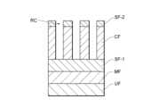
一例として、プラズマ処理チャンバ10内に準備される基板Wは、図4Aに示す断面構造を有する。基板Wは、下地膜UF、金属化合物膜MF、シリコン含有膜SF-1、炭素含有膜CF、シリコン含有膜SF-2及びマスク膜MKを含む。マスク膜MKは、マスク膜及びEUVレジスト膜の一例である。なお、シリコン含有膜SF-1及びSF-2を総称して「シリコン含有膜SF」ともいう。As an example, the substrate W prepared in the
下地膜UFは、シリコンウェハ上に形成された有機膜、誘電体膜、金属膜、半導体膜等であってよい。また、下地膜UFは、シリコンウェハであってよい。また、下地膜UFは、複数の膜が積層されて構成されてよい。The base film UF may be an organic film, a dielectric film, a metal film, a semiconductor film, or the like formed on a silicon wafer. The base film UF may also be a silicon wafer. The base film UF may also be configured by stacking multiple films.
金属化合物膜MFは、金属又は半導体を含む膜である。一例として、金属化合物MFは、多結晶シリコン膜、窒化チタン(TiN)膜、タングステンカーバイド(WC)膜又はタングステンシリサイド(WSi)膜であり得る。The metal compound film MF is a film containing a metal or a semiconductor. As an example, the metal compound MF may be a polycrystalline silicon film, a titanium nitride (TiN) film, a tungsten carbide (WC) film, or a tungsten silicide (WSi) film.
シリコン含有膜SF-1及びSF-2は、シリコン(Si)を含有する膜であり得る。シリコン含有膜SFは、シリコン酸化膜又はシリコン窒化膜を含み得る。一例として、シリコン含有膜は、SiO2膜又はSiON膜である。シリコン含有膜は、シリコンを含有する膜であれば、他の膜種を有する膜であってもよい。また、シリコン含有膜SFは、シリコン膜(例えばアモルファスシリコン膜又は多結晶シリコン膜)を含んでいてもよい。また、シリコン含有膜SFは、シリコン窒化膜、多結晶シリコン膜、炭素含有シリコン膜、及び低誘電率膜のうち少なくとも一つを含んでいてよい。炭素含有シリコン膜は、SiC膜及び/又はSiOC膜を含み得る。低誘電率膜は、シリコンを含有し、層間絶縁膜として用いられ得る。また、シリコン含有膜SFは、スピンオングラス(SOG)膜、シリコン含有反射防止(SiARC)膜であってよい。また、シリコン含有膜SF-1は、半金属及び/又は金属を含んでよい。一例として、シリコン含有膜SF-1は、SiO2膜、ホウ化シリコン膜(BSi)、タングステンシリコン膜(WSi)又はSiN膜であり得る。また、一例として、シリコン含有膜SF-2は、SOG膜、SiON膜、SiC膜、SiOC膜又はアモルファスシリコン膜であり得る。 The silicon-containing films SF-1 and SF-2 may be films containing silicon (Si). The silicon-containing film SF may include a silicon oxide film or a silicon nitride film. As an example, the silicon-containing film is a SiO2 film or a SiON film. The silicon-containing film may be a film containing other film types as long as it contains silicon. The silicon-containing film SF may also include a silicon film (e.g., an amorphous silicon film or a polycrystalline silicon film). The silicon-containing film SF may also include at least one of a silicon nitride film, a polycrystalline silicon film, a carbon-containing silicon film, and a low-k film. The carbon-containing silicon film may include a SiC film and/or a SiOC film. The low-k film contains silicon and may be used as an interlayer insulating film. The silicon-containing film SF may also be a spin-on-glass (SOG) film or a silicon-containing antireflective (SiARC) film. The silicon-containing film SF-1 may also include a semimetal and/or a metal. As an example, the silicon-containing film SF-1 may be a SiO2 film, a silicon boride film (BSi), a tungsten silicon film (WSi), or a SiN film. Also, as an example, the silicon-containing film SF-2 may be a SOG film, a SiON film, a SiC film, a SiOC film, or an amorphous silicon film.
また、シリコン含有膜SFは、互いに異なる膜種を有する二つ以上のシリコン含有膜を含んでいてもよい。二つ以上のシリコン含有膜は、シリコン酸化膜及びシリコン窒化膜を含んでいてもよい。シリコン含有膜SFは、例えば、交互に積層された一つ以上のシリコン酸化膜及び一つ以上のシリコン窒化膜を含む多層膜であってもよい。シリコン含有膜SFは、交互に積層された複数のシリコン酸化膜及び複数のシリコン窒化膜を含む多層膜であってもよい。或いは、二つ以上のシリコン含有膜は、シリコン酸化膜及びシリコン膜を含んでいてもよい。シリコン含有膜SFは、例えば、交互に積層された一つ以上のシリコン酸化膜及び一つ以上のシリコン膜を含む多層膜であってもよい。シリコン含有膜SFは、交互に積層された複数のシリコン酸化膜及び複数の多結晶シリコン膜を含む多層膜であってもよい。或いは、二つ以上のシリコン含有膜は、シリコン酸化膜、シリコン窒化膜、及びシリコン膜を含んでいてもよい。The silicon-containing film SF may also include two or more silicon-containing films having different film types. The two or more silicon-containing films may include a silicon oxide film and a silicon nitride film. The silicon-containing film SF may be, for example, a multilayer film including one or more silicon oxide films and one or more silicon nitride films that are alternately stacked. The silicon-containing film SF may be a multilayer film including a plurality of silicon oxide films and a plurality of silicon nitride films that are alternately stacked. Alternatively, the two or more silicon-containing films may include a silicon oxide film and a silicon film. The silicon-containing film SF may be, for example, a multilayer film including one or more silicon oxide films and one or more silicon films that are alternately stacked. The silicon-containing film SF may be a multilayer film including a plurality of silicon oxide films and a plurality of polycrystalline silicon films that are alternately stacked. Alternatively, the two or more silicon-containing films may include a silicon oxide film, a silicon nitride film, and a silicon film.
また、シリコン含有膜SF-1は、シリコン含有膜SF-2よりも、エッチング耐性の高い膜であってよい。当該エッチング耐性は、例えば、フルオロカーボンガス及び/又はハイドロフルオロカーボンガスを処理ガスとするエッチングにおける耐性であってよい。なお、シリコン含有膜SF-2は、シリコン含有膜SF-1よりも薄くてよい。また、シリコン含有膜SF-2は、マスク膜MK及び/又は炭素含有膜CFよりも薄くてよい。The silicon-containing film SF-1 may be a film having higher etching resistance than the silicon-containing film SF-2. The etching resistance may be, for example, resistance in etching using fluorocarbon gas and/or hydrofluorocarbon gas as the processing gas. The silicon-containing film SF-2 may be thinner than the silicon-containing film SF-1. The silicon-containing film SF-2 may be thinner than the mask film MK and/or the carbon-containing film CF.
炭素含有膜CFは、炭素を含む膜であり得る。炭素含有膜CFは、有機材料を含む膜であってよく、また、無機材料を含む膜であってよい。一例として、炭素含有膜CFは、スピンオンカーボン(SOC膜)又はアモルファスカーボン(ACL)膜である。The carbon-containing film CF may be a film containing carbon. The carbon-containing film CF may be a film containing an organic material, or may be a film containing an inorganic material. As an example, the carbon-containing film CF is a spin-on carbon (SOC film) or an amorphous carbon (ACL) film.
マスク膜MKは、金属含有膜であり得る。当該金属含有膜は、スズ含有膜であってよい。マスク膜MKは、工程ST2においてシリコン含有膜SF-2のエッチングレートよりも低いエッチングレートを有する材料から形成される。マスク膜MKは、レジスト膜であってよく、EUV用のフォトレジスト膜であってよい。一例として、EUV用のフォトレジスト膜は、スズ含有膜であり得る。一例として、スズ含有膜は、酸化スズ及び/又は水酸化スズを含み得る。また、一例として、EUV用のフォトレジスト膜は、ヨウ素(I)、テルル(Te)、アンチモン(Sb)、インジウム(In)、銀(Ag)、チタン(Ti)、クロム(Cr)、コバルト(Co)、ニッケル(Ni)、銅(Cu)、亜鉛(Zn)、ゲルマニウム(Ge)、ヒ素(As)及びハフニウム(Hf)からなる群から選択された少なくとも1つの金属を含有する金属含有膜であり得る。The mask film MK may be a metal-containing film. The metal-containing film may be a tin-containing film. The mask film MK is formed from a material having an etching rate lower than the etching rate of the silicon-containing film SF-2 in step ST2. The mask film MK may be a resist film, and may be a photoresist film for EUV. As an example, the photoresist film for EUV may be a tin-containing film. As an example, the tin-containing film may contain tin oxide and/or tin hydroxide. Also, as an example, the photoresist film for EUV may be a metal-containing film containing at least one metal selected from the group consisting of iodine (I), tellurium (Te), antimony (Sb), indium (In), silver (Ag), titanium (Ti), chromium (Cr), cobalt (Co), nickel (Ni), copper (Cu), zinc (Zn), germanium (Ge), arsenic (As), and hafnium (Hf).
マスク膜MKは、シリコン含有膜SF-2上に少なくとも1つの開口OPを規定する開口パターンを有する。マスク膜MKは、マスク膜MKの外周以外において、少なくとも1つの側壁を有する。開口OPは、当該側壁によって規定される閉じた空間である。マスク膜MKによって規定される少なくとも1つの開口OPは、基板Wの平面視において、任意の形状を有してよい。当該形状は、円形状、楕円形状、矩形形状、線形状等を含み得る。マスク膜MKが有する開口パターンは、基板Wの平面視において、ホール形状を有する複数の開口OPが規則的に配置されたアレイパターンを含み得る。当該ホール形状は、円形状、楕円形状、矩形形状等を含み得る。また、マスク膜MKが有する開口パターンは、基板Wの平面視において、線形状を有する複数の開口OPが一定の間隔で並ぶラインアンドスペース(L/S)パターンを含み得る。開口OPのピッチ(マスク膜MKの中心間距離)は100nm以下であってよい。あるいは、開口OPの幅は、30nm以下であってよい。当該幅は、開口OPがホール形状を有する場合、当該ホールの直径であってよい。また、当該幅は、開口パターンがラインアンドスペースパターンを有する場合、当該ライン又は当該スペースの幅であってよい。また、シリコン含有膜SF-1又はSF-2の厚さは、40nm以下又は20nm以下であってよい。The mask film MK has an opening pattern that defines at least one opening OP on the silicon-containing film SF-2. The mask film MK has at least one sidewall other than the outer periphery of the mask film MK. The opening OP is a closed space defined by the sidewall. The at least one opening OP defined by the mask film MK may have any shape in a planar view of the substrate W. The shape may include a circular shape, an elliptical shape, a rectangular shape, a linear shape, etc. The opening pattern of the mask film MK may include an array pattern in which a plurality of openings OP having hole shapes are regularly arranged in a planar view of the substrate W. The hole shapes may include a circular shape, an elliptical shape, a rectangular shape, etc. The opening pattern of the mask film MK may also include a line-and-space (L/S) pattern in which a plurality of openings OP having linear shapes are arranged at regular intervals in a planar view of the substrate W. The pitch of the openings OP (the center-to-center distance of the mask film MK) may be 100 nm or less. Alternatively, the width of the opening OP may be 30 nm or less. If the opening OP has a hole shape, the width may be the diameter of the hole. If the opening pattern has a line and space pattern, the width may be the width of the line or space. The thickness of the silicon-containing film SF-1 or SF-2 may be 40 nm or less or 20 nm or less.
マスク膜MKによって規定される開口OPにおいて、シリコン含有膜SF-2は、その表面(上面)が露出している。後述する工程ST2において、マスク膜MKによって規定された開口OPの形状に基づいて、シリコン含有膜SF-2、炭素含有膜CF、シリコン含有膜SF-1及び金属化合物膜MFがエッチングされる。そして、各膜にホールやトレンチ等の凹部RCが形成される。各膜に形成される1つ以上の凹部RCの各々は、基板Wの平面視において、1つ以上の開口OPの各々に基づいた形状を有する。In the opening OP defined by the mask film MK, the silicon-containing film SF-2 has its surface (upper surface) exposed. In step ST2 described below, the silicon-containing film SF-2, the carbon-containing film CF, the silicon-containing film SF-1, and the metal compound film MF are etched based on the shape of the opening OP defined by the mask film MK. Then, a recess RC such as a hole or trench is formed in each film. Each of the one or more recesses RC formed in each film has a shape based on each of the one or more openings OP in a plan view of the substrate W.
なお、マスク膜MKが有する開口パターンは、欠陥を含み得る。一例として、当該開口パターンの欠陥は、マスク膜MKに開口パターンを形成した時に発生したエッチング残渣を含み得る。エッチング残渣は、開口OPを規定するマスク膜MKの側壁や、開口OPの底部(すなわち、シリコン含有膜SF-2の表面)に存在し得る。The opening pattern of the mask film MK may include defects. As an example, the defects of the opening pattern may include etching residues that are generated when the opening pattern is formed in the mask film MK. The etching residues may be present on the sidewalls of the mask film MK that define the openings OP, or on the bottom of the openings OP (i.e., the surface of the silicon-containing film SF-2).
(工程ST2:エッチングの実行)
工程ST2において、基板Wにおいてマスク膜MKの下方に配置された各膜をエッチングする。工程ST2は、シリコン含有膜SF-2をエッチングする工程(工程ST21)、炭素含有膜CFをエッチングする工程(工程ST22)、シリコン含有膜SF-1をエッチングする工程(工程ST23)及び金属化合物膜MFをエッチングする工程(工程ST24)を有する。(Step ST2: Execution of Etching)
In step ST2, each film disposed below the mask film MK on the substrate W is etched. Step ST2 includes a step of etching the silicon-containing film SF-2 (step ST21), a step of etching the carbon-containing film CF (step ST22), a step of etching the silicon-containing film SF-1 (step ST23), and a step of etching the metal compound film MF (step ST24).
工程ST2の各工程は、プラズマ処理チャンバ10内に処理ガスを供給する工程、ソースRF信号を供給する工程及びバイアスRF信号を供給する工程を含み得る。当該各工程において、処理ガスからプラズマの活性種(イオン、ラジカル)が生成され、当該活性種によって各膜がエッチングされる。なお、処理ガス、ソースRF信号及びバイアス信号の供給が開始する順番は任意である。工程ST2の各工程において供給されるバイアス信号が有する電力の実効値(以下「電力」ともいう。)は、2kW以下又は1kW以下であり得る。なお、工程ST2における連続する2つ以上の工程に亘って、プラズマ処理チャンバ10内でプラズマが連続して生成されてよい。すなわち、連続する2つ以上の工程間において、プラズマが途切れることなく生成されてよい。これにより、プラズマ処理チャンバ10内に発生するパーティクルを低減することができる。Each step of process ST2 may include a step of supplying a processing gas into the
工程ST2の各工程において、処理ガスがプラズマ処理チャンバ10内に供給される。処理ガスの種類は、各工程においてエッチングの対象となる膜の材料、当該膜の厚さ、当該膜の上方及び/又は下方にある膜の材料、マスクとなる膜が有するパターン等に基づいて、適宜選択されてよい。In each step of process ST2, a processing gas is supplied into the
工程ST2の各工程において、プラズマ処理チャンバ10内の圧力は、適宜設定されてよい。一例として、プラズマ処理チャンバ10内の圧力は、50mTorr以下、30mTorr以下又は10mTorr以下に設定され得る。In each step of process ST2, the pressure in the
(工程ST21:シリコン含有膜SF-2のエッチング)
次に、図4Bに示すように、工程ST21において、シリコン含有膜SF-2をエッチングする。一例として、シリコン含有膜SF-2は、フルオロカーボンガス及び/又はハイドロフルオロカーボンガスを含む処理ガスから生成されたプラズマを用いてエッチングしてよい。工程ST21において、当該処理ガスから生成されたプラズマを用いて基板Wをエッチングすると、マスク膜MKをマスクとして、シリコン含有膜SF-2がエッチングされ、シリコン含有膜SF-2に凹部RCが形成される。また、凹部RCの底部において、炭素含有膜CFが露出する。なお、シリコン含有膜SF-2のエッチングにおいて、マスク膜MKの一部がエッチングされてよい。また、マスク膜MKの開口パターンが、エッチング残渣を含む欠陥を含む場合、シリコン含有膜SF-2は、当該エッチング残渣をマスクとしてエッチングされ得る。すなわち、凹部RCによってシリコン含有膜SF-2に形成されるパターンも、当該エッチング残渣に基づく欠陥を含み得る。(Step ST21: Etching of silicon-containing film SF-2)
Next, as shown in FIG. 4B, in step ST21, the silicon-containing film SF-2 is etched. As an example, the silicon-containing film SF-2 may be etched using plasma generated from a process gas containing a fluorocarbon gas and/or a hydrofluorocarbon gas. In step ST21, when the substrate W is etched using plasma generated from the process gas, the silicon-containing film SF-2 is etched using the mask film MK as a mask, and a recess RC is formed in the silicon-containing film SF-2. In addition, the carbon-containing film CF is exposed at the bottom of the recess RC. In addition, in the etching of the silicon-containing film SF-2, a part of the mask film MK may be etched. In addition, when the opening pattern of the mask film MK includes defects including etching residues, the silicon-containing film SF-2 may be etched using the etching residues as a mask. That is, the pattern formed in the silicon-containing film SF-2 by the recess RC may also include defects based on the etching residues.
(工程ST22:炭素含有膜CFのエッチング)
次に、図4Cに示すように、工程ST22において、炭素含有膜CFをエッチングする。一例として、炭素含有膜CFは、水素、ハロゲン及び酸素を含む処理ガスから生成されたプラズマを用いてエッチングしてよい。また、一例として、処理ガスは、水素、臭素、塩素及び/又はヨウ素を含有する分子からなる1以上のガスを含んでよい。一例として、当該ガスは、H2、Br2、Cl2、HBr、HCl、HI等である。処理ガスは、酸素を含有する分子からなる1以上のガスを含んでよい。一例として、当該ガスは、O2、CO2、COS等である。また、処理ガスは、He、Ar、N2等の不活性ガスを含んでよい。(Step ST22: Etching of carbon-containing film CF)
Next, as shown in FIG. 4C, in step ST22, the carbon-containing film CF is etched. As an example, the carbon-containing film CF may be etched using plasma generated from a processing gas containing hydrogen, halogen, and oxygen. Also, as an example, the processing gas may include one or more gases consisting of molecules containing hydrogen, bromine, chlorine, and/or iodine. As an example, the gas is H2 , Br2 , Cl2 , HBr, HCl, HI, etc. The processing gas may include one or more gases consisting of molecules containing oxygen. As an example, the gas is O2 , CO2 , COS, etc. Also, the processing gas may include an inert gas such as He, Ar, or N2 .
一例として、マスク膜MKがスズ含有膜である場合、工程ST22において、当該処理ガスから生成されたプラズマを用いて基板Wをエッチングすると、図4Cに示すように、マスク膜MKが除去される。そして、シリコン含有膜SF-2をマスクとして、炭素含有膜CFがエッチングされ、炭素含有膜CFに凹部RCが形成される。また、凹部RCの底部において、シリコン含有膜SF-1が露出する。なお、炭素含有膜CFのエッチングにおいて、シリコン含有膜SF-2の一部がエッチングされてよい。また、マスク膜MKの開口パターンが、エッチング残渣を含む欠陥を含む場合、炭素含有膜CFは、当該エッチング残渣に基づく欠陥を含むシリコン含有膜SF-2をマスクとしてエッチングされ得る。すなわち、凹部RCによって炭素含有膜CFに形成されるパターンも、当該エッチング残渣に基づく欠陥を含み得る。As an example, when the mask film MK is a tin-containing film, when the substrate W is etched using plasma generated from the processing gas in step ST22, the mask film MK is removed as shown in FIG. 4C. Then, the carbon-containing film CF is etched using the silicon-containing film SF-2 as a mask, and a recess RC is formed in the carbon-containing film CF. The silicon-containing film SF-1 is exposed at the bottom of the recess RC. Note that, in etching the carbon-containing film CF, a part of the silicon-containing film SF-2 may be etched. Furthermore, when the opening pattern of the mask film MK includes defects including etching residues, the carbon-containing film CF may be etched using the silicon-containing film SF-2 including defects due to the etching residues as a mask. That is, the pattern formed in the carbon-containing film CF by the recess RC may also include defects due to the etching residues.
(工程ST22:シリコン含有膜SF-1のエッチング)
次に、図4Dに示すように、工程ST23において、シリコン含有膜SF-1をエッチングする。一例として、シリコン含有膜SF-1は、炭素、水素及びフッ素を含む1以上のガスを含む処理ガスから生成されたプラズマを用いてエッチングしてよい。処理ガスは、1以上のガスを含む。ここで、当該1つ以上のガスの各々が水素、炭素及びフッ素を含んでよい。また、当該1つ以上のガスが複数のガスである場合、当該複数のガスのうち、1つのガスが、水素、炭素及びフッ素の1以上を含み、当該複数のガスのうち、残りの1つ以上のガスの一部又は全部が、水素、炭素及びフッ素の残りを含んでよい。(Step ST22: Etching of silicon-containing film SF-1)
Next, as shown in FIG. 4D, in step ST23, the silicon-containing film SF-1 is etched. As an example, the silicon-containing film SF-1 may be etched using plasma generated from a process gas containing one or more gases containing carbon, hydrogen, and fluorine. The process gas contains one or more gases. Here, each of the one or more gases may contain hydrogen, carbon, and fluorine. In addition, when the one or more gases are a plurality of gases, one gas of the plurality of gases may contain one or more of hydrogen, carbon, and fluorine, and a part or all of the remaining one or more gases of the plurality of gases may contain the remaining hydrogen, carbon, and fluorine.
工程ST23において用いられる処理ガスは、プラズマ処理中に、プラズマ処理チャンバ10内でフッ化水素(HF)種を生成可能なガスを含み得る。フッ化水素種は、工程ST23において、シリコン含有膜SF-1をエッチングするエッチャントとして機能する。The process gas used in step ST23 may include a gas capable of generating hydrogen fluoride (HF) species within the
炭素、水素及びフッ素を含むガスは、ハイドロフルオロカーボンからなる群から選択される少なくとも1種のガスであってよい。ハイドロフルオロカーボンは、例えば、CH2F2、CHF3、又はCH3Fの少なくとも一つである。ハイドロフルオロカーボンは、二つ以上の炭素原子を含んでいてもよく、二つ以上六つ以下の炭素原子を含んでいてもよい。ハイドロフルオロカーボンは、例えば、C2HF5、C2H2F4、C2H3F3、C2H4F2等の二つの炭素原子を含んでいてもよい。ハイドロフルオロカーボンは、例えば、C3HF7、C3H2F2、C3H2F4、C3H2F6、C3H3F5、C4H2F6、C4H5F5、C4H2F8等、三つの又は四つの炭素原子を含んでいてもよい。ハイドロフルオロカーボンガスは、例えば、C5H2F6、C5H2F10、C5H3F7等の五つの炭素原子を含んでもいてもよい。一実施形態として、ハイドロフルオロカーボンガスは、C3H2F4、C3H2F6、C4H2F6及びC4H2F8からなる群から選択される少なくとも1種を含む。なお、処理ガスは、プラズマ処理中にプラズマ処理チャンバ10内でフッ化水素(HF)種を生成可能なガスとして、フッ化水素(HF)を含んでよい。なお、処理ガスにおいて、フッ素原子の数に対する水素原子の数の比は、0.3以上、0.4以上又は0.5以上であってよい。また、処理ガスにおいて、炭素原子の数に対する水素原子の数の比は、1.0以上、1.5以上又は2.0以上であってよい。 The gas containing carbon, hydrogen and fluorine may be at least one gas selected from the group consisting ofhydrofluorocarbons . The hydrofluorocarbon may be, for example, at least one ofCH2F2 ,CHF3 , orCH3F . The hydrofluorocarbon may contain two or more carbon atoms, or may contain two or moreto sixor less carbon atoms. The hydrofluorocarbon may contain two carbon atoms, for example,C2HF5,C2H2F4,C2H3F3,C2H4F2,etc. The hydrofluorocarbon gas maycontainthreeorfourcarbonatoms , such as, for example,C3HF7,C3H2F2,C3H2F4,C3H2F6,C3H3F5,C4H2F6, C4H5F5,C4H2F8,etc.Thehydrofluorocarbon gas may contain five carbon atoms, such as, for example,C5H2F6,C5H2F10,C5H3F7,etc.In one embodiment, thehydrofluorocarbon gas includes at least one member selected fromthe group consisting ofC3H2F4,C3H2F6,C4H2F6,andC4H2F8. The process gas may contain hydrogen fluoride (HF) as a gas capable of generating hydrogen fluoride (HF) species in the
また、処理ガスは、水素及びフッ素を含むガスとして、プラズマ処理中に、プラズマ処理チャンバ10内でフッ化水素種を生成可能な混合ガスを含んでよい。フッ化水素種を生成可能な混合ガスは、水素源及びフッ素源を含んでよい。水素源は、例えば、H2、NH3、H2O、H2O2又はハイドロカーボン(CH4、C3H6等)であってよい。フッ素源は、BF3、NF3、PF3、PF5、SF6、WF6、XeF2又はフルオロカーボンであってよい。一例として、フッ化水素種を生成可能な混合ガスは、三フッ化窒素(NF3)と水素(H2)との混合ガスである。 The process gas may also include a gas mixture capable of generating hydrogen fluoride species in the
また、処理ガスは、炭素を含むガスとして、ハイドロカーボン(CxHy)、フルオロカーボン(CvFw)からなる群から選択される少なくとも一種の炭素含有ガスを含んでいてもよい。ここで、x、y、v及びwの各々は自然数である。ハイドロカーボンは、例えば、CH4、C2H6、C3H6、C3H8又はC4H10等を含んでもよい。フルオロカーボンは、例えば、CF4、C2F2、C2F4、C3F8、C4F6、C4F8又はC5F8等を含んでもよい。これらの炭素含有ガスから生成される化学種は、マスク膜MKを保護し得る。 The process gas may contain at least one carbon-containing gas selected from the group consisting of hydrocarbons (CxHy ) and fluorocarbons (CvFw ), where x,y ,v , and w are each a natural number. The hydrocarbon may contain, for example,CH4 ,C2H6 ,C3H6 ,C3H8 , orC4H10.The fluorocarbonmay contain, for example, CF4, C2F2, C2F4, C3F8, C4F6, C4F8, or C5F8.Chemicalspeciesgeneratedfromthesecarbon-containinggasesmay protectthe mask filmMK.
炭素を含むガスは、不飽和結合を有する直鎖状のものであってもよい。不飽和結合を有する直鎖状の炭素含有ガスとして、例えば、C3F6(ヘキサフルオロプロパン)ガス、C4F8(オクタフルオロ-1-ブテン、オクタフルオロ-2-ブテン)ガス、C3H2F4(1,3,3,3-テトラフルオロプロペン)ガス、C4H2F6(トランス-1,1,1,4,4,4-ヘキサフルオロ-2-ブテン)ガス、C4F8O(ペンタフルオロエチルトリフルオロビニルエーテル)ガス、CF3COFガス(1,2,2,2-テトラフルオロエタン-1-オン)、CHF2COF(ジフルオロ酢酸フルオライド)ガス及びCOF2(フッ化カルボニル)ガスからなる群から選択される少なくとも1種を用いてもよい。これらのガスは、地球温暖化係数(GWP)が比較的低いガスであるため、温室効果の改善に有意である。 The carbon-containing gas may be a linear gas having an unsaturated bond. As the linear carbon-containing gas having an unsaturated bond, for example, at least one selected from the group consisting of C3 F6 (hexafluoropropane) gas, C4 F8 (octafluoro-1-butene, octafluoro-2-butene) gas, C3 H2 F4 (1,3,3,3-tetrafluoropropene) gas, C4 H2 F6 (trans-1,1,1,4,4,4-hexafluoro-2-butene) gas, C4 F8 O (pentafluoroethyl trifluorovinyl ether) gas, CF3 COF gas (1,2,2,2-tetrafluoroethane-1-one), CHF2 COF (difluoroacetic acid fluoride) gas, and COF2 (carbonyl fluoride) gas may be used. These gases have a relatively low global warming potential (GWP) and are therefore significant in improving the greenhouse effect.
また、処理ガスは、少なくとも一つのリン含有分子を更に含み得る。リン含有分子は、十酸化四リン(P4O10)、八酸化四リン(P4O8)、六酸化四リン(P4O6)等の酸化物であってもよい。十酸化四リンは、五酸化二リン(P2O5)と呼ばれることがある。リン含有分子は、三フッ化リン(PF3)、五フッ化リン(PF5)、三塩化リン(PCl3)、五塩化リン(PCl5)、三臭化リン(PBr3)、五臭化リン(PBr5)、ヨウ化リン(PI3)のようなハロゲン化物(ハロゲン化リン)であってもよい。即ち、リンを含む分子は、ハロゲン元素としてフッ素を含むフッ化物(フッ化リン)であってもよい。或いは、リンを含む分子は、ハロゲン元素としてフッ素以外のハロゲン元素を含んでもよい。リン含有分子は、フッ化ホスホリル(POF3)、塩化ホスホリル(POCl3)、臭化ホスホリル(POBr3)のようなハロゲン化ホスホリルであってよい。リン含有分子は、ホスフィン(PH3)、リン化カルシウム(Ca3P2等)、リン酸(H3PO4)、リン酸ナトリウム(Na3PO4)、ヘキサフルオロリン酸(HPF6)等であってよい。リン含有分子は、フルオロホスフィン類(HxPFy)であってよい。ここで、xとyの和は、3又は5である。フルオロホスフィン類としては、HPF2、H2PF3が例示される。処理ガスは、少なくとも一つのリン含有分子として、上記のリン含有分子のうち一つ以上のリン含有分子を含み得る。例えば、処理ガスは、少なくとも一つのリン含有分子として、PF3、PCl3、PF5,PCl5,POCl3、PH3、PBr3、又はPBr5の少なくとも一つを含み得る。また、少なくとも一つのリン含有分子として、PClaFb(a及びbは正の整数)及びPCcHdFe(c、d及びeは正の整数)からなる群から選択される少なくとも一つを含み得る。なお、処理ガスに含まれる各リン含有分子が液体又は固体である場合、各リン含有分子は、加熱等によって気化されてプラズマ処理チャンバ10内に供給され得る。 The process gas may further include at least one phosphorus-containing molecule. The phosphorus-containing molecule may be an oxide such as tetraphosphorus decaoxide (P4 O10 ), tetraphosphorus octoxide (P4 O8 ), or tetraphosphorus hexaoxide (P4 O6 ). Tetraphosphorus decaoxide is sometimes called diphosphorus pentoxide (P2 O5 ). The phosphorus-containing molecule may be a halide (phosphorus halide) such as phosphorus trifluoride (PF3 ), phosphorus pentafluoride (PF5 ), phosphorus trichloride (PCl3 ), phosphorus pentachloride (PCl5 ), phosphorus tribromide (PBr3 ), phosphorus pentabromide (PBr5 ), or phosphorus iodide (PI3 ). That is, the phosphorus-containing molecule may be a fluoride (phosphorus fluoride) containing fluorine as the halogen element. Alternatively, the phosphorus-containing molecule may contain a halogen element other than fluorine as the halogen element. The phosphorus-containing molecule may be a phosphoryl halide such as phosphoryl fluoride (POF3 ), phosphoryl chloride (POCl3 ), or phosphoryl bromide (POBr3 ). The phosphorus-containing molecule may be phosphine (PH3 ),calciumphosphide (Ca3P2 , etc.), phosphoric acid (H3PO4 ), sodium phosphate (Na3PO4 ), hexafluorophosphoric acid (HPF6 ), or the like. The phosphorus-containing molecule may be afluorophosphine (HxPFy ), where the sum of x andy is 3 or5. Examples of the fluorophosphine includeHPF2 andH2PF3 . The process gas may contain one or more of the above phosphorus-containing molecules as at least one phosphorus-containing molecule. For example, the process gas may contain at least one ofPF3 ,PCl3 ,PF5 ,PCl5 ,POCl3 ,PH3 ,PBr3 , orPBr5 as the at least one phosphorus-containing molecule. In addition, the processgas may contain at least one selected from the group consisting ofPClaFb (a and b are positive integers) andPCcHdFe (c,d, and e are positive integers) as the at least one phosphorus-containing molecule. When each phosphorus-containing molecule contained in the process gas is liquid or solid, each phosphorus-containing molecule may be vaporized by heating or the like and supplied into the
また、処理ガスは、ハロゲン含有分子を含んでもよい。ハロゲン含有分子は、炭素を含有しなくてもよい。ハロゲン含有分子は、フッ素含有分子であってよく、フッ素以外のハロゲン元素を含有するハロゲン含有分子であってもよい。フッ素含有分子は、例えば、三フッ化窒素(NF3)、六フッ化硫黄(SF6)、三フッ化ホウ素(BF3)などのガスを含んでいてもよい。フッ素以外のハロゲン元素を含有するハロゲン含有分子は、例えば、塩素含有ガス、臭素含有ガス及びヨウ素からなる群から選択される少なくとも1種であってよい。塩素含有ガスは、例えば、塩素(Cl2)、二塩化ケイ素(SiCl2)、四塩化ケイ素(SiCl4)、四塩化炭素(CCl4)、ジシクロロシラン(SiH2Cl2)、六塩化二ケイ素(Si2Cl6)、クロロホルム(CHCl3)、塩化スルフリル(SO2Cl2)、三塩化ホウ素(BCl3)などのガスである。臭素含有ガスは、例えば、臭素(Br2)、臭化水素(HBr)、ジブロモジフルオロメタン(CBr2F2)、ブロモペンタフルオロエタン(C2F5Br)三臭化リン(PBr3)、五臭化リン(PBr5)、リン酸オキシブロミド(POBr3)、三臭化ホウ素(BBr3)などのガスである。ヨウ素含有ガスは、例えば、ヨウ化水素(HI)、トリフルオロヨードメタン(CF3I)、ペンタフルオロヨードエタン(C2F5I)、ヘプタフルオロプロピルヨージド(C3F7I)、五フッ化ヨウ素(IF5)、七フッ化ヨウ素(IF7)、ヨウ素(I2)、三ヨウ化リン(PI3)などのガスである。これらのハロゲン含有分子はから生成される化学種は、プラズマエッチングで形成される凹部の形状を制御するために用いられ得る。 The process gas may also include a halogen-containing molecule. The halogen-containing molecule may not include carbon. The halogen-containing molecule may be a fluorine-containing molecule, or may be a halogen-containing molecule containing a halogen element other than fluorine. The fluorine-containing molecule may include gases such as nitrogen trifluoride (NF3 ), sulfur hexafluoride (SF6 ), and boron trifluoride (BF3 ). The halogen-containing molecule containing a halogen element other than fluorine may be at least one selected from the group consisting of a chlorine-containing gas, a bromine-containing gas, and iodine. Examples of the chlorine-containing gas include chlorine (Cl2 ), silicon dichloride (SiCl2 ), silicon tetrachloride (SiCl4 ), carbon tetrachloride (CCl4 ), dicyclosilane (SiH2Cl2 ), siliconhexachloride (Si2Cl6 ), chloroform (CHCl3 ), sulfuryl chloride (SO2Cl2 ), boron trichloride (BCl3 ), etc. Examples of the bromine-containing gas include bromine (Br2 ),hydrogen bromide (HBr), dibromodifluoromethane (CBr2F2 ), bromopentafluoroethane(C2F5Br ), phosphorus tribromide (PBr3 ), phosphorus pentabromide (PBr5 ), phosphoric oxybromide (POBr3 ), boron tribromide (BBr3 ), etc. Examples of iodine-containing gases include hydrogen iodide (HI), trifluoroiodomethane (CF3I ), pentafluoroiodoethane (C2F5I ), heptafluoropropyl iodide (C3F7I ), iodine pentafluoride (IF5 ), iodine heptafluoride (IF7 ), iodine(I2 ), phosphorus triiodide (PI3 ), etc. Chemical species generated from these halogen-containing molecules can be used to control the shape ofrecesses formed by plasma etching.
処理ガスは、酸素含有分子を含んでよい。酸素含有分子は、例えばO2、CO2又はCOを含んでいてもよい。また、処理ガスは、Ar、Kr、Xe等の貴ガスを含んでよい。 The process gas may include oxygen-containing molecules, such asO2 ,CO2 , or CO. The process gas may also include noble gases, such as Ar, Kr, and Xe.
また、図2のプラズマ処理装置1において、処理ガスは、中央ガス注入部131及びサイドガス注入部の一方又は双方から、プラズマ処理チャンバ10内に供給されてよい。一例として、中央ガス注入部131から供給される炭素含有ガスの流量よりも、サイドガス注入部から供給される炭素含有ガスの流量が多くてよい。即ち、処理ガスに含まれる炭素含有ガスの流量に対する、中央ガス注入部131から供給される炭素含有ガスの流量の割合が50%以下、サイドガス注入部から供給される炭素含有ガスの流量の割合が50%以上であってよい。また、処理ガスに含まれる炭素含有ガスの流量に対する、中央ガス注入部131から供給される炭素含有ガスの流量の割合が20%以下、サイドガス注入部から供給される炭素含有ガスの流量の割合が80%以上であってよい。また、処理ガスに含まれる炭素含有ガスの流量に対する、中央ガス注入部131から供給される炭素含有ガスの流量の割合が10%以下、サイドガス注入部から供給される炭素含有ガスの流量の割合が90%以上であってよい。また、処理ガスに含まれる炭素含有ガスの流量に対する、中央ガス注入部131から供給される炭素含有ガスの流量の割合が5%以下、サイドガス注入部から供給される炭素含有ガスの流量の割合が95%以上であってよい。また、処理ガスに含まれる炭素含有ガスの流量における、サイドガス注入部から供給される炭素含有ガスの流量の割合が100%であってよい。2, the processing gas may be supplied into the
また、一例として、プラズマ処理チャンバ10内に供給される処理ガスのうち、中央ガス注入部131から供給される炭素含有ガスに含まれる炭素原子の数よりも、サイドガス注入部から供給される炭素含有ガスに含まれる炭素原子の数が多くてよい。As another example, among the processing gases supplied into the
処理ガスに含まれる炭素含有ガスの少なくとも一部を、サイドガス注入部からプラズマ処理チャンバ10内に供給することにより、基板Wの面内において、エッチング膜のエッチングレートの均一性及び/又はエッチング膜に形成される凹部の寸法の均一性を向上することができる。By supplying at least a portion of the carbon-containing gas contained in the processing gas into the
次に、工程ST23において供給されるソースRF信号及びバイアス信号について説明する。工程ST23において供給されるソースRF信号は、一例として、図2のプラズマ処理装置1における上部電極又は図2におけるプラズマ処理装置1のアンテナ14に供給され得る。上部電極は電極の一例である。ソースRF信号は、RFの連続波であってよく、また、パルス波であってもよい。ソースRF信号の電力は、バイアス信号の電力よりも大きい。一例として、ソースRF信号の電力は、300W以上であってよい。また、ソースRF信号の電力は、500W以上、1,000W以上、又は、2,000W以上であってよい。Next, the source RF signal and bias signal supplied in step ST23 will be described. As an example, the source RF signal supplied in step ST23 may be supplied to the upper electrode in the
工程ST23において供給されるバイアス信号は、一例として、図2の基板支持部11に供給される。バイアス信号は、基板支持部11においてバイアス電極として機能し得る部材に供給されてよい。バイアス信号は、RF信号であり得る。バイアス信号の電力は、ソースRF信号の電力よりも小さい。一例として、バイアス信号の電力は、200W以下であってよい。また、バイアス信号の電力は、100W以下、又は、50W以下であってよい。なお、一例として、バイアス信号の電力は、ソースRF信号の電力よりも大きくてもよい。The bias signal supplied in step ST23 is supplied to the
工程ST23において、処理ガスから生成されたプラズマを用いて基板Wをエッチングすると、シリコン含有膜SF-2及び/又は炭素含有膜CFをマスクとして、シリコン含有膜SF-1がエッチングされ、シリコン含有膜SF-1に凹部RCが形成される。また、凹部RCの底部において、金属化合物MFが露出する。なお、シリコン含有膜SF-2は、シリコン含有膜SF-1と同様のエッチング条件でエッチングされ得る。当該エッチング条件は、処理ガスの種類、ソースRF信号の電力、バイアス信号の電力、プラズマ処理チャンバ10内の圧力を含み得る。In step ST23, when the substrate W is etched using plasma generated from the processing gas, the silicon-containing film SF-1 is etched using the silicon-containing film SF-2 and/or the carbon-containing film CF as a mask, and a recess RC is formed in the silicon-containing film SF-1. In addition, the metal compound MF is exposed at the bottom of the recess RC. The silicon-containing film SF-2 can be etched under the same etching conditions as the silicon-containing film SF-1. The etching conditions can include the type of processing gas, the power of the source RF signal, the power of the bias signal, and the pressure in the
なお、工程ST23において、工程ST21及び/又は工程ST22において生成された、金属を含有する堆積物を除去してよい。当該金属は、マスク膜MKに含まれる金属であってよい。また、一例として、当該金属は、スズ(Sn)であってよい。当該堆積物は、工程ST21及び/又は工程ST22のエッチングにおいて生じた、当該金属を含む化合物等の残渣であってよい。また、当該堆積物は、基板Wに付着した堆積物であってよく、また、プラズマ処理チャンバ10の内壁に付着した堆積物であってよい。In addition, in step ST23, metal-containing deposits generated in step ST21 and/or step ST22 may be removed. The metal may be a metal contained in the mask film MK. As an example, the metal may be tin (Sn). The deposits may be residues of compounds containing the metal that are generated during the etching in step ST21 and/or step ST22. The deposits may be deposits attached to the substrate W, or may be deposits attached to the inner wall of the
本処理方法では、バイアス信号の電力を比較的低くしてシリコン含有膜をエッチングする。すなわち、処理ガスから生成されたフッ化水素種が有するエネルギーを低く抑えることができる。これにより、EUVレジスト等のマスク膜が有する開口パターンを、シリコン含有膜に適切に形成することができる。In this processing method, the power of the bias signal is relatively low to etch the silicon-containing film. In other words, the energy of the hydrogen fluoride species generated from the processing gas can be kept low. This allows the opening pattern of a mask film such as an EUV resist to be appropriately formed in the silicon-containing film.
また、本処理方法では、マスク膜MKが金属を含有する場合、当該金属を含む堆積物及び/又はマスク膜MKに含まれる欠陥を除去しつつ、シリコン含有膜SFをエッチングすることができる。これにより、シリコン含有膜SFのエッチングにおいて、当該堆積物及び/又は当該欠陥の影響を低減できるので、シリコン含有膜SFに含まれる欠陥を低減することができる。なお、当該堆積物は、基板Wに含まれる他の膜をエッチングする工程において生成された、当該金属を含む化合物等であり得る。また、当該欠陥は、マスク膜MKに開口パターンを形成する工程で生成した、マスク膜MKのエッチング残渣であり得る。In addition, in this processing method, when the mask film MK contains a metal, the silicon-containing film SF can be etched while removing deposits containing the metal and/or defects contained in the mask film MK. This reduces the influence of the deposits and/or defects in the etching of the silicon-containing film SF, thereby reducing the defects contained in the silicon-containing film SF. The deposits may be compounds containing the metal that are generated in the process of etching another film included in the substrate W. The defects may be etching residues of the mask film MK that are generated in the process of forming an opening pattern in the mask film MK.
また、本処理方法では、当該堆積物及び/又は当該欠陥を除去しつつ、シリコン含有膜SFをエッチングできるので、シリコン含有膜SFが有するパターンの粗さを改善することができる。In addition, this processing method can etch the silicon-containing film SF while removing the deposits and/or defects, thereby improving the roughness of the pattern of the silicon-containing film SF.
以上の各実施形態は、説明の目的で説明されており、本開示の範囲を限定することを意図するものではない。各実施形態は、本開示の範囲及び趣旨から逸脱することなく種々の変形をなし得る。例えば、ある実施形態における一部の構成要素を、他の実施形態に追加することができる。また、ある実施形態における一部の構成要素を、他の実施形態の対応する構成要素と置換することができる。一例として、本開示は以下の形態を含み得る。The above embodiments are described for the purpose of explanation and are not intended to limit the scope of the present disclosure. Various modifications of the embodiments may be made without departing from the scope and spirit of the present disclosure. For example, some components in one embodiment may be added to another embodiment. Also, some components in one embodiment may be replaced with corresponding components in another embodiment. As an example, the present disclosure may include the following forms:
(付記1)
プラズマ処理装置において実行されるプラズマ処理方法であって、
前記プラズマ処理装置は、チャンバ及び前記チャンバ内に設けられた基板支持部を有し、
前記プラズマ処理方法は、
(a)シリコン含有膜及び前記シリコン含有膜上のマスク膜を有する基板を前記基板支持部に準備する工程であって、前記マスク膜は開口パターンを含む、準備工程と、
(b)前記チャンバ内でプラズマを生成して、前記シリコン含有膜をエッチングして前記シリコン含有膜に前記開口パターンを形成する工程と
を含み、
前記(b)の工程は、
(b-1)フッ化水素を含む処理ガスを前記チャンバ内に供給する工程と、
(b-2)前記チャンバ内で前記処理ガスからプラズマを生成する工程と、
(b-3)前記基板支持部にバイアス信号を供給する工程であって、前記バイアス信号が有する電力の実効値は2kW以下である、工程と
を含む、プラズマ処理方法。(Appendix 1)
A plasma processing method performed in a plasma processing apparatus, comprising:
The plasma processing apparatus includes a chamber and a substrate support provided in the chamber,
The plasma processing method includes:
(a) preparing a substrate having a silicon-containing film and a mask film on the silicon-containing film on the substrate support, the mask film including an opening pattern;
(b) generating a plasma in the chamber to etch the silicon-containing film to form the opening pattern in the silicon-containing film;
The step (b) comprises:
(b-1) supplying a process gas containing hydrogen fluoride into the chamber;
(b-2) generating a plasma from the process gas in the chamber;
(b-3) a step of supplying a bias signal to the substrate supporting portion, the bias signal having an effective power value of 2 kW or less.
(付記2)
前記マスクは、レジスト膜である、付記1に記載のプラズマ処理方法。(Appendix 2)
2. The plasma processing method according to
(付記3)
前記マスクは、EUVレジスト膜である、付記1に記載のプラズマ処理方法。(Appendix 3)
2. The plasma processing method according to
(付記4)
前記開口パターンに含まれる開口の幅は、30nm以下である、付記1から3のいずれか1つに記載のプラズマ処理方法。(Appendix 4)
4. The plasma processing method according to
(付記5)
前記(b-2)の工程において、前記実効値は、1kW以下である、付記1から4のいずれか1つに記載のプラズマ処理方法。(Appendix 5)
5. The plasma processing method according to
(付記6)
前記基板支持部は前記基板を支持する基板支持面において複数のゾーンを含み、
前記(a)の工程は、前記基板支持部の温度を、前記ゾーン単位で設定する工程を含み、
前記(b)の工程において、前記シリコン含有膜は、前記基板支持部の温度がゾーン単位で設定された状態でエッチングされる、付記1から5のいずれか1つに記載のプラズマ処理方法。(Appendix 6)
the substrate support includes a plurality of zones in a substrate support surface for supporting the substrate;
The step (a) includes a step of setting a temperature of the substrate support part on a zone-by-zone basis;
6. The plasma processing method according to
(付記7)
前記基板支持部は、1又は複数のヒータを含み、前記基板の温度を調節するように構成された温調モジュールを備え、
前記(b)の工程は、前記温調モジュールにより、前記基板支持体の温度が80℃以下に設定された状態で実行される、付記1から5のいずれか1つに記載のプラズマ処理方法。(Appendix 7)
the substrate support comprises a temperature regulation module including one or more heaters and configured to regulate a temperature of the substrate;
6. The plasma processing method according to
(付記8)
前記処理ガスは、炭素含有ガスを含む、付記1から7のいずれか1つに記載のプラズマ処理方法。(Appendix 8)
8. The plasma processing method of
(付記9)
前記処理ガスは、リン含有ガスを含む、付記1から8のいずれか1つに記載のプラズマ処理方法。(Appendix 9)
9. The plasma processing method of
(付記10)
前記処理ガスは、タングステン含有ガス、ホウ素含有ガス及び酸素含有ガスからなる群から選択される少なくとも1種のガスを含む、付記1から9のいずれか1つに記載のプラズマ処理方法。(Appendix 10)
10. The plasma processing method according to
(付記11)
前記処理ガスは、ハロゲン含有分子を含む、付記1から10のいずれか1つに記載のプラズマ処理方法。(Appendix 11)
11. The plasma processing method of
(付記12)
前記処理ガスは、不活性ガスを含む、付記1から11のいずれか1つに記載のプラズマ処理方法。(Appendix 12)
12. The plasma processing method of
(付記13)
前記処理ガスは、フッ化水素ガスを含む、付記1から12のいずれか1つに記載のプラズマ処理方法。(Appendix 13)
13. The plasma processing method according to
(付記14)
前記処理ガスに含まれるガスのうち、前記フッ化水素ガスの流量が最も多い、付記13に記載のプラズマ処理方法。(Appendix 14)
14. The plasma processing method according to claim 13, wherein the hydrogen fluoride gas has the highest flow rate among gases contained in the processing gas.
(付記15)
前記プラズマ処理装置は、
前記基板支持部に対向して、前記チャンバの上面に配置された第1のガス注入部と、
前記チャンバの側面に配置された第2のガス注入部と
を有し、
前記処理ガスは、炭素を含む少なくとも1種のガス及び炭素を含まない少なくとも1種のガスを含み、
前記炭素を含む少なくとも1種のガスの少なくとも1種は、前記第1のガス注入部から供給され、
前記炭素を含まない少なくとも1種のガスの少なくとも1種は、前記第2のガス注入部から供給される、付記1から14のいずれか1つに記載のプラズマ処理方法。(Appendix 15)
The plasma processing apparatus includes:
a first gas injection portion disposed on an upper surface of the chamber opposite the substrate support;
a second gas injection port disposed on a side of the chamber;
the process gas comprises at least one gas containing carbon and at least one gas not containing carbon;
At least one of the at least one gas containing carbon is supplied from the first gas injection part;
15. The plasma processing method according to any one of
(付記16)
前記プラズマ処理装置は、
前記チャンバ内において前記チャンバの上面に配置された第1のガス注入部と、
前記チャンバ内において前記チャンバの側面に配置された第2のガス注入部と
を有し、
前記処理ガスは、少なくとも1種の炭素含有ガスを含み、
前記少なくとも1種の炭素含有ガスは、前記第1のガス注入部及び前記第2のガス注入部から前記チャンバ内に供給され、
前記第2のガス注入部から前記チャンバ内に供給される前記少なくとも1種の炭素含有ガスの流量は、前記第1のガス注入部から前記チャンバ内に供給される前記少なくとも1種の炭素含有ガスの流量よりも多い、付記1から15のいずれか1つに記載のプラズマ処理方法。(Appendix 16)
The plasma processing apparatus includes:
a first gas injection port disposed within the chamber on an upper surface of the chamber;
a second gas injection port disposed within the chamber on a side of the chamber;
the process gas comprises at least one carbon-containing gas;
the at least one carbon-containing gas is supplied into the chamber from the first gas inlet and the second gas inlet;
16. The plasma processing method according to
(付記17)
前記(b)において、前記チャンバ内の圧力は50mTorr以下に設定される、付記1から15のいずれか1つに記載のプラズマ処理方法。(Appendix 17)
16. The plasma processing method according to
(付記18)
前記EUVレジストは、有機膜レジストである、付記3に記載のプラズマ処理方法。(Appendix 18)
4. The plasma processing method according to claim 3, wherein the EUV resist is an organic film resist.
(付記19)
前記EUVレジストは、金属含有レジストである、付記3に記載のプラズマ処理方法。(Appendix 19)
4. The plasma processing method of claim 3, wherein the EUV resist is a metal-containing resist.
(付記20)
前記シリコン含有膜の厚さは、40nm以下である、付記1から19のいずれか1つに記載のプラズマ処理方法。(Appendix 20)
20. The plasma processing method of
(付記21)
前記シリコン含有膜の厚さは、20nm以下である、付記20に記載のプラズマ処理方法。(Appendix 21)
21. The plasma processing method of
(付記22)
プラズマ処理装置において実行されるプラズマ処理方法であって、
前記プラズマ処理装置は、チャンバ及び前記チャンバ内に設けられた基板支持部を有し、
前記プラズマ処理方法は、
(a)シリコン含有膜及び前記シリコン含有膜上のマスク膜を有する基板を前記基板支持部に準備する工程であって、前記マスク膜は開口パターンを含む、準備工程と、
(b)前記チャンバ内でプラズマを生成して、前記シリコン含有膜をエッチングして前記シリコン含有膜に前記開口パターンを形成する工程と
を含み、
前記(a)の工程において、前記開口パターンに含まれる開口の幅は30nm以下であり、
前記(b)の工程は、
(b-1)少なくとも水素及びフッ素を含む処理ガスを前記チャンバ内に供給する工程と、
(b-2)前記チャンバ内で前記処理ガスからフッ化水素種を含むプラズマを生成する工程と、
(b-3)前記基板支持部にバイアス信号を供給する工程であって、前記バイアス信号が有する電力の実効値は2kW以下である、工程と
を含む、プラズマ処理方法。(Appendix 22)
A plasma processing method performed in a plasma processing apparatus, comprising:
The plasma processing apparatus includes a chamber and a substrate support provided in the chamber,
The plasma processing method includes:
(a) preparing a substrate having a silicon-containing film and a mask film on the silicon-containing film on the substrate support, the mask film including an opening pattern;
(b) generating a plasma in the chamber to etch the silicon-containing film to form the opening pattern in the silicon-containing film;
In the step (a), the width of the opening included in the opening pattern is 30 nm or less;
The step (b) comprises:
(b-1) supplying a process gas containing at least hydrogen and fluorine into the chamber;
(b-2) generating a plasma containing hydrogen fluoride species from the process gas in the chamber;
(b-3) a step of supplying a bias signal to the substrate supporting portion, the bias signal having an effective power value of 2 kW or less.
(付記23)
プラズマ処理装置において実行されるプラズマ処理方法であって、
前記プラズマ処理装置は、チャンバ及び前記チャンバ内に設けられた基板支持部を有し、
前記プラズマ処理方法は、
(a)第1のシリコン含有膜と、前記第1のシリコン含有膜上の炭素含有膜と、前記炭素含有膜上の第2のシリコン含有膜と、前記第2のシリコン含有膜上のレジスト膜とを有する基板を準備する工程であって、前記レジスト膜は、開口幅が30nm以下の開口パターンを含む、準備工程と、
(b)前記開口パターンを介して、前記第2のシリコン含有膜をエッチングし、前記第2のシリコン含有膜に第1の凹部を形成する工程と、
(c)前記第1の凹部を介して、前記炭素含有膜をエッチングし、前記炭素含有膜に第2の凹部を形成する工程と、
(d)前記第2の凹部を介して、前記第1のシリコン含有膜をエッチングし、前記第1のエッチング含有膜に第3の凹部を形成する工程と、
を含み、
前記(b)、(c)及び(d)において、前記基板支持部にバイアス信号が供給され、
前記(d)は、
(d-1)少なくとも水素及びフッ素を含む処理ガスを前記チャンバ内に供給する工程と、
(d-2)前記チャンバ内で前記処理ガスからフッ化水素種を含むプラズマを生成する工程と
を含む、プラズマ処理方法。(Appendix 23)
A plasma processing method performed in a plasma processing apparatus, comprising:
The plasma processing apparatus includes a chamber and a substrate support provided in the chamber,
The plasma processing method includes:
(a) preparing a substrate having a first silicon-containing film, a carbon-containing film on the first silicon-containing film, a second silicon-containing film on the carbon-containing film, and a resist film on the second silicon-containing film, the resist film including an opening pattern having an opening width of 30 nm or less;
(b) etching the second silicon-containing film through the opening pattern to form a first recess in the second silicon-containing film;
(c) etching the carbon-containing film through the first recess to form a second recess in the carbon-containing film;
(d) etching the first silicon-containing film through the second recess to form a third recess in the first etch-containing film;
Including,
In the steps (b), (c) and (d), a bias signal is provided to the substrate support;
The (d) is
(d-1) supplying a process gas containing at least hydrogen and fluorine into the chamber;
(d-2) generating a plasma containing hydrogen fluoride species from the process gas in the chamber.
(付記24)
前記バイアス信号は、2kW以下の実効値を有するRF信号である、付記22に記載のプラズマ処理方法。(Appendix 24)
23. The plasma processing method of
(付記25)
前記バイアス信号は、パルス化されたバイアスDC信号である、付記22又は23に記載のプラズマ処理方法。(Appendix 25)
24. The plasma processing method of
(付記26)
前記(b)、(c)及び(d)において、連続する2つ以上の工程に亘って、プラズマが連続して生成される、付記22から25のいずれか1つに記載のプラズマ処理方法。(Appendix 26)
26. The plasma processing method according to any one of
(付記27)
前記第1のシリコン含有膜又は前記第2のシリコン含有膜の厚さは40nm以下である、付記22から26のいずれか1つに記載のプラズマ処理方法。(Appendix 27)
27. The plasma processing method of any one of
(付記28)
前記レジスト膜が有する前記開口パターンは欠陥を含む、付記22から27のいずれか1つに記載のプラズマ処理方法。(Appendix 28)
28. The plasma processing method according to
(付記29)
チャンバ、ガス供給部、プラズマ生成部、前記チャンバ内に設けられた基板支持部及び制御部を備えるプラズマ処理装置であって、
前記制御部は、
(a)シリコン含有膜及び前記シリコン含有膜上のマスク膜を有する基板であって、前記マスク膜は開口パターンを含む、基板を前記基板支持部に準備する制御と、
(b)前記チャンバ内でプラズマを生成して、前記シリコン含有膜をエッチングして前記シリコン含有膜に前記開口パターンを形成する制御と
を実行し、
前記(b)において、前記制御部は、
(b-1)フッ化水素を含む処理ガスを前記チャンバ内に供給する制御と、
(b-2)前記チャンバ内で前記処理ガスからフッ化水素種を含むプラズマを生成する制御と、
(b-3)前記基板支持部にバイアス信号を供給する制御であって、前記バイアス信号が有する電力の実効値は2kW以下である、制御と
を実行する、プラズマ処理装置。(Appendix 29)
A plasma processing apparatus comprising a chamber, a gas supply unit, a plasma generating unit, a substrate supporting unit and a control unit provided in the chamber,
The control unit is
(a) controlling a substrate having a silicon-containing film and a mask film on the silicon-containing film, the mask film including an opening pattern, on the substrate support;
(b) generating a plasma in the chamber to etch the silicon-containing film to form the opening pattern in the silicon-containing film;
In the (b), the control unit
(b-1) controlling a supply of a process gas containing hydrogen fluoride into the chamber;
(b-2) generating a plasma containing hydrogen fluoride species from the process gas in the chamber; and
(b-3) Control of supplying a bias signal to the substrate supporting portion, the bias signal having an effective value of power of 2 kW or less.
1…プラズマ処理装置、2…制御部、10…プラズマ処理チャンバ、12…プラズマ生成部、13…中央ガス注入部、14…アンテナ、20…ガス供給部、30…電源、31…RF電源、32…DC電源、52…周辺ガス注入部、101…誘電体窓、102…側壁、111…本体部、111a…中央領域、111b…環状領域、131…中央ガス注入部、CF…炭素含有膜、MF…金属化合物膜、MK…マスク膜、OP…開口、RC…凹部、SF…シリコン含有膜、UF…下地膜1...plasma processing device, 2...control unit, 10...plasma processing chamber, 12...plasma generation unit, 13...central gas injection unit, 14...antenna, 20...gas supply unit, 30...power source, 31...RF power source, 32...DC power source, 52...peripheral gas injection unit, 101...dielectric window, 102...side wall, 111...main body, 111a...central region, 111b...annular region, 131...central gas injection unit, CF...carbon-containing film, MF...metal compound film, MK...mask film, OP...opening, RC...recess, SF...silicon-containing film, UF...undercoat film
Claims (23)
Translated fromJapanese前記プラズマ処理装置は、チャンバと、前記チャンバ内に設けられた基板支持部と、前記基板支持部に対向して配置される上部電極又はアンテナを含むプラズマ生成部とを有し、
前記プラズマ処理方法は、
(a)シリコン含有膜(ただし、有機成分及びシリカ成分を主成分とする有機無機複合膜を除く。)及び前記シリコン含有膜上のマスク膜を有する基板を前記基板支持部に準備する工程であって、前記マスク膜は開口パターンを含む、準備工程と、
(b)前記チャンバ内でプラズマを生成して、前記シリコン含有膜をエッチングして前記シリコン含有膜に前記開口パターンを形成する工程と
を含み、
前記(b)の工程は、
(b-1)フッ化水素ガスを含む処理ガスを前記チャンバ内に供給する工程であって、前記処理ガスに含まれるガスのうち前記フッ化水素ガスの流量が最も多い、工程と、
(b-2)前記プラズマ生成部にソースRF信号を供給して、前記チャンバ内で前記処理ガスからプラズマを生成する工程と、
(b-3)前記基板支持部にバイアス信号を供給する工程であって、前記バイアス信号が有する電力の実効値は1kW以下である、工程と
を含み、
前記ソースRF信号の電力は、前記バイアス信号の電力よりも大きい、
プラズマ処理方法。 A plasma processing method performed in a plasma processing apparatus, comprising:
The plasma processing apparatus includes a chamber, a substrate support provided in the chamber, and a plasma generating unit including an upper electrode or an antenna disposed opposite to the substrate support,
The plasma processing method includes:
(a) preparing a substrate having a silicon-containing film (excluding an organic-inorganic composite film mainly composed of an organic component and a silica component) and a mask film on the silicon-containing film on the substrate support, the mask film including an opening pattern;
(b) generating a plasma in the chamber to etch the silicon-containing film to form the opening pattern in the silicon-containing film;
The step (b) comprises:
(b-1) supplying a process gas containing hydrogen fluoride gas into the chamber, the process gas having a largest flow rate of the hydrogen fluoride gas;
(b-2) supplying a source RF signal to the plasma generating unit to generate plasma from the processing gas in the chamber;
(b-3) supplying a bias signal to the substrate support, the bias signal having an effective power value of 1 kW or less;
the power of the source RF signal is greater than the power of the bias signal;
Plasma treatment method.
前記(a)の工程は、前記基板支持部の温度を、前記ゾーン単位で設定する工程を含み、
前記(b)の工程において、前記シリコン含有膜は、前記基板支持部の温度がゾーン単位で設定された状態でエッチングされる、請求項1に記載のプラズマ処理方法。 the substrate support includes a plurality of zones in a substrate support surface for supporting the substrate;
The step (a) includes a step of setting a temperature of the substrate support part on a zone-by-zone basis;
2. The plasma processing method according to claim 1, wherein in the step (b), the silicon-containing film is etched in a state in which a temperature of the substrate supporting part is set in zone units.
前記(b)の工程は、前記温調モジュールにより、前記基板支持部の温度が80℃以下に設定された状態で実行される、請求項1に記載のプラズマ処理方法。 the substrate support comprises a temperature regulation module including one or more heaters and configured to regulate a temperature of the substrate;
2. The plasma processing method according to claim 1, wherein the step (b) is performed in a state where the temperature of the substrate support part is set to 80° C. or lower by the temperature adjustment module.
前記プラズマ処理装置は、チャンバ及び前記チャンバ内に設けられた基板支持部を有し、
前記プラズマ処理方法は、
(a)シリコン含有膜及び前記シリコン含有膜上のマスク膜を有する基板を前記基板支持部に準備する工程であって、前記マスク膜は開口パターンを含む、準備工程と、
(b)前記チャンバ内でプラズマを生成して、前記シリコン含有膜をエッチングして前記シリコン含有膜に前記開口パターンを形成する工程と
を含み、
前記(b)の工程は、
(b-1)フッ化水素を含む処理ガスを前記チャンバ内に供給する工程と、
(b-2)前記チャンバ内で前記処理ガスからプラズマを生成する工程と、
(b-3)前記基板支持部にバイアス信号を供給する工程であって、前記バイアス信号が有する電力の実効値は2kW以下である、工程と
を含み、
前記プラズマ処理装置は、
前記基板支持部に対向して、前記チャンバの上面に配置された第1のガス注入部と、
前記チャンバの側面に配置された第2のガス注入部と
を有し、
前記処理ガスは、炭素を含む少なくとも1種のガス及び炭素を含まない少なくとも1種のガス(フッ化水素を除く)を含み、
前記炭素を含む少なくとも1種のガスの少なくとも1種は、前記第1のガス注入部から供給され、
前記炭素を含まない少なくとも1種のガスの少なくとも1種は、前記第2のガス注入部から供給される、プラズマ処理方法。 A plasma processing method performed in a plasma processing apparatus, comprising:
The plasma processing apparatus includes a chamber and a substrate support provided in the chamber,
The plasma processing method includes:
(a) preparing a substrate having a silicon-containing film and a mask film on the silicon-containing film on the substrate support, the mask film including an opening pattern;
(b) generating a plasma in the chamber to etch the silicon-containing film to form the opening pattern in the silicon-containing film;
The step (b) comprises:
(b-1) supplying a process gas containing hydrogen fluoride into the chamber;
(b-2) generating a plasma from the process gas in the chamber;
(b-3) supplying a bias signal to the substrate support, the bias signal having an effective power value of 2 kW or less;
The plasma processing apparatus includes:
a first gas injection portion disposed on an upper surface of the chamber opposite the substrate support;
a second gas injection port disposed on a side of the chamber;
the process gas comprises at least one gas containing carbon and at least one gas not containing carbon(excluding hydrogen fluoride) ;
At least one of the at least one gas containing carbon is supplied from the first gas injection part;
At least one of the at least one carbon-free gases is supplied from the second gas injection part.
前記プラズマ処理装置は、チャンバ及び前記チャンバ内に設けられた基板支持部を有し、
前記プラズマ処理方法は、
(a)シリコン含有膜及び前記シリコン含有膜上のマスク膜を有する基板を前記基板支持部に準備する工程であって、前記マスク膜は開口パターンを含む、準備工程と、
(b)前記チャンバ内でプラズマを生成して、前記シリコン含有膜をエッチングして前記シリコン含有膜に前記開口パターンを形成する工程と
を含み、
前記(b)の工程は、
(b-1)フッ化水素を含む処理ガスを前記チャンバ内に供給する工程と、
(b-2)前記チャンバ内で前記処理ガスからプラズマを生成する工程と、
(b-3)前記基板支持部にバイアス信号を供給する工程であって、前記バイアス信号が有する電力の実効値は2kW以下である、工程と
を含み、
前記プラズマ処理装置は、
前記チャンバ内において前記チャンバの上面に配置された第1のガス注入部と、
前記チャンバ内において前記チャンバの側面に配置された第2のガス注入部と
を有し、
前記処理ガスは、少なくとも1種の炭素含有ガスを含み、
前記少なくとも1種の炭素含有ガスは、前記第1のガス注入部及び前記第2のガス注入部から前記チャンバ内に供給され、
前記第2のガス注入部から前記チャンバ内に供給される前記少なくとも1種の炭素含有ガスの流量は、前記第1のガス注入部から前記チャンバ内に供給される前記少なくとも1種の炭素含有ガスの流量よりも多い、プラズマ処理方法。 A plasma processing method performed in a plasma processing apparatus, comprising:
The plasma processing apparatus includes a chamber and a substrate support provided in the chamber,
The plasma processing method includes:
(a) preparing a substrate having a silicon-containing film and a mask film on the silicon-containing film on the substrate support, the mask film including an opening pattern;
(b) generating a plasma in the chamber to etch the silicon-containing film to form the opening pattern in the silicon-containing film;
The step (b) comprises:
(b-1) supplying a process gas containing hydrogen fluoride into the chamber;
(b-2) generating a plasma from the process gas in the chamber;
(b-3) supplying a bias signal to the substrate support, the bias signal having an effective power value of 2 kW or less;
The plasma processing apparatus includes:
a first gas injection port disposed within the chamber on an upper surface of the chamber;
a second gas injection port disposed within the chamber on a side of the chamber;
the process gas comprises at least one carbon-containing gas;
the at least one carbon-containing gas is supplied into the chamber from the first gas inlet and the second gas inlet;
a flow rate of the at least one carbon-containing gas supplied into the chamber from the second gas injection part is greater than a flow rate of the at least one carbon-containing gas supplied into the chamber from the first gas injection part.
前記制御部は、
(a)シリコン含有膜(ただし、有機成分及びシリカ成分を主成分とする有機無機複合膜を除く。)及び前記シリコン含有膜上のマスク膜を有する基板であって、前記マスク膜は開口パターンを含む、基板を前記基板支持部に準備する制御と、
(b)前記チャンバ内でプラズマを生成して、前記シリコン含有膜をエッチングして前記シリコン含有膜に前記開口パターンを形成する制御と
を実行し、
前記(b)において、前記制御部は、
(b-1)フッ化水素ガスを含む処理ガスを前記チャンバ内に供給する制御であって、前記処理ガスに含まれるガスのうち前記フッ化水素ガスの流量が最も多い、制御と、
(b-2)前記プラズマ生成部にソースRF信号を供給して、前記チャンバ内で前記処理ガスからフッ化水素種を含むプラズマを生成する制御と、
(b-3)前記基板支持部にバイアス信号を供給する制御であって、前記バイアス信号が有する電力の実効値は1kW以下である、制御と
を実行し、
前記ソースRF信号の電力は、前記バイアス信号の電力よりも大きい、
プラズマ処理装置。 A plasma processing apparatus comprising: a chamber; a gas supply unit; a substrate support unit provided in the chamber; a plasma generating unit including an upper electrode or an antenna disposed opposite the substrate support unit; and a control unit,
The control unit is
(a) controlling a substrate having a silicon-containing film (excluding an organic-inorganic composite film mainly composed of an organic component and a silica component) and a mask film on the silicon-containing film, the mask film including an opening pattern, on the substrate support;
(b) generating a plasma in the chamber to etch the silicon-containing film to form the opening pattern in the silicon-containing film;
In the (b), the control unit
(b-1) control of supplying a process gas containing hydrogen fluoride gas into the chamber, in which the flow rate of the hydrogen fluoride gas is the highest among gases contained in the process gas; and
(b-2) supplying a source RF signal to the plasma generating unit to generate plasma containing hydrogen fluoride species from the processing gas in the chamber;
(b-3) controlling a bias signal to be supplied to the substrate support, the bias signal having an effective power value of 1 kW or less;
the power of the source RF signal is greater than the power of the bias signal;
Plasma processing equipment.
前記プラズマ処理装置は、チャンバと、前記チャンバ内に設けられた基板支持部と、前記基板支持部に対向して配置される上部電極又はアンテナを含むプラズマ生成部とを有し、
前記プラズマ処理方法は、
(a)シリコン含有膜及び前記シリコン含有膜上のマスク膜を有する基板を前記基板支持部に準備する工程であって、前記マスク膜は開口パターンを含む、準備工程と、
(b)前記チャンバ内でプラズマを生成して、前記シリコン含有膜をエッチングして前記シリコン含有膜に前記開口パターンを形成する工程と
を含み、
前記(b)の工程は、
(b-1)フッ化水素及び酸素含有ガス(ただし、炭酸ガス及び一酸化炭素ガスを除く。)を含む処理ガスを前記チャンバ内に供給する工程と、
(b-2)前記プラズマ生成部にソースRF信号を供給して、前記チャンバ内で前記処理ガスからプラズマを生成する工程と、
(b-3)前記基板支持部にバイアス信号を供給する工程であって、前記バイアス信号が有する電力の実効値は1kW以下である、工程と
を含み、
前記ソースRF信号の電力は、前記バイアス信号の電力よりも大きい、
プラズマ処理方法。 A plasma processing method performed in a plasma processing apparatus, comprising:
The plasma processing apparatus includes a chamber, a substrate support provided in the chamber, and a plasma generating unit including an upper electrode or an antenna disposed opposite to the substrate support,
The plasma processing method includes:
(a) preparing a substrate having a silicon-containing film and a mask film on the silicon-containing film on the substrate support, the mask film including an opening pattern;
(b) generating a plasma in the chamber to etch the silicon-containing film to form the opening pattern in the silicon-containing film;
The step (b) comprises:
(b-1) supplying a process gas containing hydrogen fluoride and an oxygen-containing gas (excluding carbon dioxide gas and carbon monoxide gas) into the chamber;
(b-2) supplying a source RF signal to the plasma generating unit to generate plasma from the processing gas in the chamber;
(b-3) supplying a bias signal to the substrate support, the bias signal having an effective power value of 1 kW or less;
the power of the source RF signal is greater than the power of the bias signal;
Plasma treatment method.
前記制御部は、
(a)シリコン含有膜及び前記シリコン含有膜上のマスク膜を有する基板であって、前記マスク膜は開口パターンを含む、基板を前記基板支持部に準備する制御と、
(b)前記チャンバ内でプラズマを生成して、前記シリコン含有膜をエッチングして前記シリコン含有膜に前記開口パターンを形成する制御と
を実行し、
前記(b)において、前記制御部は、
(b-1)フッ化水素及び酸素含有ガス(ただし、炭酸ガス及び一酸化炭素ガスを除く。)を含む処理ガスを前記チャンバ内に供給する制御と、
(b-2)前記プラズマ生成部にソースRF信号を供給して、前記チャンバ内で前記処理ガスからフッ化水素種を含むプラズマを生成する制御と、
(b-3)前記基板支持部にバイアス信号を供給する制御であって、前記バイアス信号が有する電力の実効値は1kW以下である、制御と
を実行し、
前記ソースRF信号の電力は、前記バイアス信号の電力よりも大きい、
プラズマ処理装置。 A plasma processing apparatus comprising: a chamber; a gas supply unit; a substrate support unit provided in the chamber; a plasma generating unit including an upper electrode or an antenna disposed opposite the substrate support unit; and a control unit,
The control unit is
(a) controlling a substrate having a silicon-containing film and a mask film on the silicon-containing film, the mask film including an opening pattern, on the substrate support;
(b) generating a plasma in the chamber to etch the silicon-containing film to form the opening pattern in the silicon-containing film;
In the (b), the control unit
(b-1) supplying a process gas containing hydrogen fluoride and an oxygen-containing gas (excluding carbon dioxide gas and carbon monoxide gas) into the chamber;
(b-2) supplying a source RF signal to the plasma generating unit to generate plasma containing hydrogen fluoride species from the processing gas in the chamber;
(b-3) controlling a bias signal to be supplied to the substrate support, the bias signal having an effective power value of 1 kW or less;
the power of the source RF signal is greater than the power of the bias signal;
Plasma processing equipment.
Priority Applications (1)
| Application Number | Priority Date | Filing Date | Title |
|---|---|---|---|
| JP2023063808AJP7536941B2 (en) | 2022-08-30 | 2023-04-11 | Plasma processing method and plasma processing apparatus |
Applications Claiming Priority (2)
| Application Number | Priority Date | Filing Date | Title |
|---|---|---|---|
| JP2022136874 | 2022-08-30 | ||
| JP2023063808AJP7536941B2 (en) | 2022-08-30 | 2023-04-11 | Plasma processing method and plasma processing apparatus |
Related Parent Applications (1)
| Application Number | Title | Priority Date | Filing Date |
|---|---|---|---|
| JP2022136874Division | 2022-08-30 | 2022-08-30 |
Publications (2)
| Publication Number | Publication Date |
|---|---|
| JP2024035044A JP2024035044A (en) | 2024-03-13 |
| JP7536941B2true JP7536941B2 (en) | 2024-08-20 |
Family
ID=90099600
Family Applications (2)
| Application Number | Title | Priority Date | Filing Date |
|---|---|---|---|
| JP2023063808AActiveJP7536941B2 (en) | 2022-08-30 | 2023-04-11 | Plasma processing method and plasma processing apparatus |
| JP2024544261APendingJPWO2024048543A1 (en) | 2022-08-30 | 2023-08-29 |
Family Applications After (1)
| Application Number | Title | Priority Date | Filing Date |
|---|---|---|---|
| JP2024544261APendingJPWO2024048543A1 (en) | 2022-08-30 | 2023-08-29 |
Country Status (6)
| Country | Link |
|---|---|
| US (1) | US20250210327A1 (en) |
| JP (2) | JP7536941B2 (en) |
| KR (1) | KR20250056947A (en) |
| CN (1) | CN119895546A (en) |
| TW (1) | TW202418390A (en) |
| WO (1) | WO2024048543A1 (en) |
Citations (7)
| Publication number | Priority date | Publication date | Assignee | Title |
|---|---|---|---|---|
| JP2000216135A (en) | 1999-01-27 | 2000-08-04 | Matsushita Electric Ind Co Ltd | Etching method |
| JP2001035920A (en) | 1999-07-19 | 2001-02-09 | Mitsubishi Electric Corp | Method for manufacturing semiconductor device |
| JP2003524703A (en) | 1998-12-14 | 2003-08-19 | アプライド マテリアルズ インコーポレイテッド | High temperature chemical vapor deposition chamber |
| JP2016213339A (en) | 2015-05-11 | 2016-12-15 | 東京エレクトロン株式会社 | Method for processing workpiece |
| WO2021090798A1 (en) | 2019-11-08 | 2021-05-14 | 東京エレクトロン株式会社 | Etching method |
| JP2021086849A (en) | 2019-11-25 | 2021-06-03 | 東京エレクトロン株式会社 | Etching method and etching device |
| WO2022164820A1 (en) | 2021-01-29 | 2022-08-04 | Tokyo Electron Limited | Cyclic plasma etch process |
Family Cites Families (9)
| Publication number | Priority date | Publication date | Assignee | Title |
|---|---|---|---|---|
| US7723235B2 (en)* | 2004-09-17 | 2010-05-25 | Renesas Technology Corp. | Method for smoothing a resist pattern prior to etching a layer using the resist pattern |
| JP5140568B2 (en)* | 2008-12-04 | 2013-02-06 | 株式会社アルバック | Etching method of multilayer film |
| JP6454492B2 (en) | 2014-08-08 | 2019-01-16 | 東京エレクトロン株式会社 | Method for etching a multilayer film |
| JP6366454B2 (en)* | 2014-10-07 | 2018-08-01 | 東京エレクトロン株式会社 | Method for processing an object |
| JP7330079B2 (en)* | 2019-11-28 | 2023-08-21 | 東京エレクトロン株式会社 | Plasma processing equipment |
| JP6956288B2 (en)* | 2020-04-30 | 2021-11-02 | 東京エレクトロン株式会社 | Substrate processing method, plasma processing equipment, and etching gas composition |
| JP7325477B2 (en)* | 2020-08-12 | 2023-08-14 | 東京エレクトロン株式会社 | Etching method and plasma etching apparatus |
| JP7374058B2 (en)* | 2020-09-18 | 2023-11-06 | 東京エレクトロン株式会社 | Etching method and plasma processing equipment |
| US20220165578A1 (en)* | 2020-11-25 | 2022-05-26 | Tokyo Electron Limited | Substrate processing method and substrate processing apparatus |
- 2023
- 2023-04-11JPJP2023063808Apatent/JP7536941B2/enactiveActive
- 2023-08-29JPJP2024544261Apatent/JPWO2024048543A1/jaactivePending
- 2023-08-29KRKR1020257009386Apatent/KR20250056947A/enactivePending
- 2023-08-29CNCN202380060904.0Apatent/CN119895546A/enactivePending
- 2023-08-29WOPCT/JP2023/031083patent/WO2024048543A1/ennot_activeCeased
- 2023-08-30TWTW112132697Apatent/TW202418390A/enunknown
- 2025
- 2025-02-27USUS19/065,059patent/US20250210327A1/enactivePending
Patent Citations (7)
| Publication number | Priority date | Publication date | Assignee | Title |
|---|---|---|---|---|
| JP2003524703A (en) | 1998-12-14 | 2003-08-19 | アプライド マテリアルズ インコーポレイテッド | High temperature chemical vapor deposition chamber |
| JP2000216135A (en) | 1999-01-27 | 2000-08-04 | Matsushita Electric Ind Co Ltd | Etching method |
| JP2001035920A (en) | 1999-07-19 | 2001-02-09 | Mitsubishi Electric Corp | Method for manufacturing semiconductor device |
| JP2016213339A (en) | 2015-05-11 | 2016-12-15 | 東京エレクトロン株式会社 | Method for processing workpiece |
| WO2021090798A1 (en) | 2019-11-08 | 2021-05-14 | 東京エレクトロン株式会社 | Etching method |
| JP2021086849A (en) | 2019-11-25 | 2021-06-03 | 東京エレクトロン株式会社 | Etching method and etching device |
| WO2022164820A1 (en) | 2021-01-29 | 2022-08-04 | Tokyo Electron Limited | Cyclic plasma etch process |
Also Published As
| Publication number | Publication date |
|---|---|
| JP2024035044A (en) | 2024-03-13 |
| TW202418390A (en) | 2024-05-01 |
| CN119895546A (en) | 2025-04-25 |
| JPWO2024048543A1 (en) | 2024-03-07 |
| WO2024048543A1 (en) | 2024-03-07 |
| KR20250056947A (en) | 2025-04-28 |
| US20250210327A1 (en) | 2025-06-26 |
Similar Documents
| Publication | Publication Date | Title |
|---|---|---|
| JP7599872B2 (en) | Etching method and plasma processing apparatus | |
| JP7672943B2 (en) | Plasma processing apparatus and substrate processing method | |
| JP7336623B2 (en) | Etching method | |
| JP7746343B2 (en) | Plasma processing apparatus, etching method, semiconductor device manufacturing method, program, and storage medium | |
| JP2022172753A (en) | Substrate processing method and substrate processing apparatus | |
| JP2023127546A (en) | Plasma processing method and plasma processing device | |
| US12354837B2 (en) | Plasma processing method and plasma processing apparatus | |
| JP7536941B2 (en) | Plasma processing method and plasma processing apparatus | |
| TW202412058A (en) | Plasma processing method, and plasma processing system | |
| JP2023171277A (en) | Plasma processing method and plasma processing apparatus | |
| CN117096027A (en) | Plasma processing method and plasma processing system | |
| US20250191927A1 (en) | Etching method and plasma processing system | |
| TW202443688A (en) | Etching method and plasma processing device | |
| WO2023238903A1 (en) | Etching method and plasma treatment device | |
| CN116705601A (en) | Plasma treatment method and plasma treatment apparatus | |
| TW202425126A (en) | Etching method and plasma processing device | |
| JP2023171269A (en) | Etching method and plasma treatment system | |
| WO2025150267A1 (en) | Plasma processing device and plasma processing method | |
| JP2024176159A (en) | Plasma processing method and plasma processing apparatus | |
| WO2025089101A1 (en) | Plasma processing method and plasma processing apparatus | |
| TW202507839A (en) | Etching method and etching device | |
| JP2024053353A (en) | Etching method and plasma processing system | |
| JP2024054083A (en) | Plasma processing system, plasma processing apparatus and etching method | |
| TW202533314A (en) | Plasma treatment method and plasma treatment device | |
| CN117855088A (en) | Plasma processing system, plasma processing apparatus, and etching method |
Legal Events
| Date | Code | Title | Description |
|---|---|---|---|
| A621 | Written request for application examination | Free format text:JAPANESE INTERMEDIATE CODE: A621 Effective date:20230411 | |
| A871 | Explanation of circumstances concerning accelerated examination | Free format text:JAPANESE INTERMEDIATE CODE: A871 Effective date:20230411 | |
| A131 | Notification of reasons for refusal | Free format text:JAPANESE INTERMEDIATE CODE: A131 Effective date:20230508 | |
| A521 | Request for written amendment filed | Free format text:JAPANESE INTERMEDIATE CODE: A523 Effective date:20230706 | |
| A131 | Notification of reasons for refusal | Free format text:JAPANESE INTERMEDIATE CODE: A131 Effective date:20230804 | |
| A521 | Request for written amendment filed | Free format text:JAPANESE INTERMEDIATE CODE: A523 Effective date:20231003 | |
| A02 | Decision of refusal | Free format text:JAPANESE INTERMEDIATE CODE: A02 Effective date:20231109 | |
| A521 | Request for written amendment filed | Free format text:JAPANESE INTERMEDIATE CODE: A523 Effective date:20240209 | |
| A911 | Transfer to examiner for re-examination before appeal (zenchi) | Free format text:JAPANESE INTERMEDIATE CODE: A911 Effective date:20240220 | |
| A912 | Re-examination (zenchi) completed and case transferred to appeal board | Free format text:JAPANESE INTERMEDIATE CODE: A912 Effective date:20240308 | |
| A521 | Request for written amendment filed | Free format text:JAPANESE INTERMEDIATE CODE: A523 Effective date:20240508 | |
| A61 | First payment of annual fees (during grant procedure) | Free format text:JAPANESE INTERMEDIATE CODE: A61 Effective date:20240807 | |
| R150 | Certificate of patent or registration of utility model | Ref document number:7536941 Country of ref document:JP Free format text:JAPANESE INTERMEDIATE CODE: R150 |