JP7535175B2 - Etching Method - Google Patents
Etching MethodDownload PDFInfo
- Publication number
- JP7535175B2 JP7535175B2JP2023511863AJP2023511863AJP7535175B2JP 7535175 B2JP7535175 B2JP 7535175B2JP 2023511863 AJP2023511863 AJP 2023511863AJP 2023511863 AJP2023511863 AJP 2023511863AJP 7535175 B2JP7535175 B2JP 7535175B2
- Authority
- JP
- Japan
- Prior art keywords
- layer
- etching
- wafer
- sige
- film
- Prior art date
- Legal status (The legal status is an assumption and is not a legal conclusion. Google has not performed a legal analysis and makes no representation as to the accuracy of the status listed.)
- Active
Links
Images


Classifications
- H—ELECTRICITY
- H01—ELECTRIC ELEMENTS
- H01L—SEMICONDUCTOR DEVICES NOT COVERED BY CLASS H10
- H01L21/00—Processes or apparatus adapted for the manufacture or treatment of semiconductor or solid state devices or of parts thereof
- H01L21/02—Manufacture or treatment of semiconductor devices or of parts thereof
- H01L21/04—Manufacture or treatment of semiconductor devices or of parts thereof the devices having potential barriers, e.g. a PN junction, depletion layer or carrier concentration layer
- H01L21/18—Manufacture or treatment of semiconductor devices or of parts thereof the devices having potential barriers, e.g. a PN junction, depletion layer or carrier concentration layer the devices having semiconductor bodies comprising elements of Group IV of the Periodic Table or AIIIBV compounds with or without impurities, e.g. doping materials
- H01L21/30—Treatment of semiconductor bodies using processes or apparatus not provided for in groups H01L21/20 - H01L21/26
- H01L21/302—Treatment of semiconductor bodies using processes or apparatus not provided for in groups H01L21/20 - H01L21/26 to change their surface-physical characteristics or shape, e.g. etching, polishing, cutting
- H01L21/306—Chemical or electrical treatment, e.g. electrolytic etching
- H01L21/3065—Plasma etching; Reactive-ion etching
- H—ELECTRICITY
- H10—SEMICONDUCTOR DEVICES; ELECTRIC SOLID-STATE DEVICES NOT OTHERWISE PROVIDED FOR
- H10D—INORGANIC ELECTRIC SEMICONDUCTOR DEVICES
- H10D30/00—Field-effect transistors [FET]
- H10D30/01—Manufacture or treatment
- H10D30/014—Manufacture or treatment of FETs having zero-dimensional [0D] or one-dimensional [1D] channels, e.g. quantum wire FETs, single-electron transistors [SET] or Coulomb blockade transistors
- H—ELECTRICITY
- H10—SEMICONDUCTOR DEVICES; ELECTRIC SOLID-STATE DEVICES NOT OTHERWISE PROVIDED FOR
- H10D—INORGANIC ELECTRIC SEMICONDUCTOR DEVICES
- H10D84/00—Integrated devices formed in or on semiconductor substrates that comprise only semiconducting layers, e.g. on Si wafers or on GaAs-on-Si wafers
- H10D84/01—Manufacture or treatment
- H10D84/0123—Integrating together multiple components covered by H10D12/00 or H10D30/00, e.g. integrating multiple IGBTs
- H10D84/0126—Integrating together multiple components covered by H10D12/00 or H10D30/00, e.g. integrating multiple IGBTs the components including insulated gates, e.g. IGFETs
- H10D84/0128—Manufacturing their channels
Landscapes
- Engineering & Computer Science (AREA)
- Physics & Mathematics (AREA)
- Plasma & Fusion (AREA)
- Condensed Matter Physics & Semiconductors (AREA)
- General Physics & Mathematics (AREA)
- Manufacturing & Machinery (AREA)
- Computer Hardware Design (AREA)
- Microelectronics & Electronic Packaging (AREA)
- Power Engineering (AREA)
- Drying Of Semiconductors (AREA)
Description
Translated fromJapanese本発明は、プラズマを用いた半導体を含む処理対象の膜層、例えば、SiGeおよびGeのエッチング方法に関する。The present invention relates to a method for etching a film layer to be processed, including a semiconductor, such as SiGe and Ge, using plasma.
半導体デバイスの微細化と三次元化による集積度向上が進められており、ロジックデバイスでは14nmノード以降、電界効果トランジスタ(FET: Field Effect Transistor)の構造が二次元プレーナ型から三次元フィン型に移行した。更なる集積度向上に向けて現在、ゲートオールアラウンド(GAA:Gate All Around)型FETの開発が進められている。GAA型FETは、チャネルの周囲が完全にゲートで囲まれた構造を持ち、ナノシートと呼ばれる薄膜状のチャネル、あるいはナノワイヤと呼ばれる細線状のチャネルを垂直方向に多数積層した構造を持つ。そのチャネル材料としては現在Siが用いられており、技術ノードが5nm以降の次世代においては、シリコン(Si)よりも移動度の高いゲルマニウム(Ge)をチャネル材料として用いる方式が有望視されている。The integration level of semiconductor devices is increasing due to miniaturization and three-dimensionalization. In logic devices, the structure of field effect transistors (FETs) has shifted from two-dimensional planar type to three-dimensional fin type since the 14 nm node. To further improve integration level, Gate All Around (GAA) FETs are currently being developed. GAA FETs have a structure in which the channel is completely surrounded by a gate, and have a structure in which a thin-film channel called a nanosheet or a thin-wire channel called a nanowire is stacked vertically in large numbers. Currently, Si is used as the channel material, and in the next generation of technology nodes of 5 nm and later, a method of using germanium (Ge), which has a higher mobility than silicon (Si), as the channel material is expected to be promising.
チャネル材料としてSiを用いる場合の、GAA型FETの製造プロセスでは、まずチャネル材料として用いるSiの層と、犠牲層として用いるシリコンゲルマニウム(SiGe)の層を、交互にエピタキシャル成長した多層構造を作製する。次に、この多層構造を異方性ドライエッチングした後、犠牲層であるSiGe層を、Siチャネル層に対して選択的に等方性エッチングする。そして、SiGe層をエッチングした領域に、インナースペーサを充填し、ソースやドレイン、ゲート電極を形成することでSiをチャネル材料とするGAA型FETが完成する。In the manufacturing process of a GAA FET using Si as the channel material, first, a multilayer structure is created by epitaxially growing alternate layers of Si used as the channel material and silicon germanium (SiGe) used as the sacrificial layer. Next, this multilayer structure is anisotropically dry etched, and then the sacrificial SiGe layer is isotropically etched selectively with respect to the Si channel layer. Then, an inner spacer is filled into the etched area of the SiGe layer, and the source, drain, and gate electrodes are formed to complete a GAA FET with Si as the channel material.
一方、技術ノードが5nm以降の次世代で有力となる新たなチャネル材料であるGeを用いる場合には、Siをチャネル材料とする場合とは異なる多層構造と作製プロセスが用いられる。チャネル材料としてGeを用いる場合の、GAA型FETの製造プロセスでは、まずチャネル材料として用いるGeの層と、犠牲層として用いるSiGeの層を、交互にエピタキシャル成長した多層構造を作製する。次に、この多層構造を異方性ドライエッチングした後、犠牲層であるSiGe層を、Geチャネル層に対して選択的に等方性エッチングする。そして、SiGe層をエッチングした領域に、インナースペーサを充填し、ソースやドレイン、ゲート電極を形成することでGeをチャネル材料とするGAA型FETが完成する。On the other hand, when Ge is used, which is a new channel material that will be the leading material in the next generation of technology nodes from 5 nm onwards, a multilayer structure and fabrication process different from the case of using Si as the channel material are used. In the manufacturing process of a GAA FET when Ge is used as the channel material, a multilayer structure is first fabricated by epitaxially growing alternately a layer of Ge used as the channel material and a layer of SiGe used as the sacrificial layer. Next, this multilayer structure is anisotropically dry etched, and then the SiGe layer, which is the sacrificial layer, is selectively isotropically etched with respect to the Ge channel layer. Then, the area where the SiGe layer is etched is filled with an inner spacer, and the source, drain and gate electrodes are formed to complete a GAA FET with Ge as the channel material.
SiGeをSiに対して選択的にエッチングする技術としては、例えばフッ化水素(HF)と過酸化水素(H2O2)、酢酸(CH3COOH)の混合液を用いる方法が用いられてきた。しかし、加工寸法の微細化が進んだことと、アスペクト比の高い三次元構造が用いられるようになったことで、ウェット処理では薬液の表面張力によるパターン倒壊の問題などが顕在化している。例えばシリコンの高アスペクト比パターンを用いた場合には、パターン間隔を狭くしていった際に、リンス液乾燥時の表面張力で倒壊が始まるパターン間隔の限界値が、アスペクト比の二乗に比例して大きくなると報告されている。このため、薬液を用いずに各種膜を等方的にエッチングするプロセス手法の開発が強く望まれてきた。これに対応して、薬液を用いずプラズマを用いて、均一性良くSiGeを等方的にエッチングする従来の技術として、たとえば、特開2021-150488号公報(特許文献1)や、米国特許出願公開第2018/0218915号明細書(特許文献2)が提案されている。 As a technique for selectively etching SiGe with respect to Si, for example, a method using a mixture of hydrogen fluoride (HF), hydrogen peroxide (H2 O2 ), and acetic acid (CH3 COOH) has been used. However, as the processing dimensions have become finer and three-dimensional structures with high aspect ratios have come to be used, problems such as pattern collapse due to the surface tension of the chemical solution have become apparent in wet processing. For example, when a high aspect ratio silicon pattern is used, it has been reported that the limit value of the pattern interval at which collapse begins due to the surface tension during drying of the rinse solution increases in proportion to the square of the aspect ratio when the pattern interval is narrowed. For this reason, there has been a strong demand for the development of a process method for isotropically etching various films without using chemical solutions. In response to this, for example, JP 2021-150488 A (Patent Document 1) and U.S. Patent Application Publication No. 2018/0218915 (Patent Document 2) have been proposed as conventional techniques for isotropically etching SiGe with good uniformity using plasma without using chemical solutions.
特許文献1には、第一のステップで、フッ素と酸素のラジカルを含むリモートプラズマを用いてSiGeの表面を酸化した後に、第二のステップでHF/NH3ガス処理(NH3:アンモニア)と加熱処理により酸化膜を除去するサイクルを繰り返し、SiGeをSiに対して選択的にエッチングする技術が開示されている。
特許文献2には、第一のステップで、水素を含むプラズマによりSiGe表面を還元処理した後、第二のステップで酸素を含むプラズマによりSiGe表面を酸化処理し、第三のステップで加熱するサイクルを繰り返し、SiGeをSiに対して選択的にエッチングする技術が開示されている。
上記の従来技術では、次の点について考慮されていなかったため、次世代デバイスの開発にあたって問題が生じた。The above conventional technologies did not take into account the following points, which caused problems in developing next-generation devices:
すなわち、上記従来の技術では、SiGeをSiに対して選択的かつ均一性良くサイクルエッチングする技術を開示しているものの、SiGeをGeに対して選択的かつ均一性良くサイクルエッチングする技術は考慮されていなかった。このため、技術ノードが5nm以降の世代で有力となる、Geをチャネル材料とするGAA型FETの製造プロセスには対応できないという問題があった。従来の技術では、SiGe表面に酸化物を生成し、これを除去することでSiに対して選択的なエッチングを実現している。この技術は、膜中のGe含有量が多いほどSiGeの表面酸化が進みやすいことや、Geの酸化物の揮発性が、Si酸化物の揮発性よりも高い性質を利用している。しかしながら、このような従来のSiGeの原子層エッチングを、次世代のGeをチャネル材料とGAA型FET製造に適用すると、SiGe犠牲層をエッチングする際に、エッチング量を極力抑制して、エッチングせずに残すべきGeチャネル層のエッチングが進んでしまい、Geチャネル層が意図せず除去されてしまうという問題があった。That is, in the above conventional technology, although a technology for selectively and uniformly cyclically etching SiGe with respect to Si is disclosed, a technology for selectively and uniformly cyclically etching SiGe with respect to Ge was not considered. Therefore, there was a problem that it cannot be used for the manufacturing process of GAA type FETs using Ge as a channel material, which will be dominant in the technology node generation of 5 nm and later. In the conventional technology, selective etching with respect to Si is realized by generating an oxide on the SiGe surface and removing it. This technology utilizes the property that the higher the Ge content in the film, the more likely the SiGe surface oxidation is to proceed, and that the volatility of Ge oxide is higher than that of Si oxide. However, when such conventional atomic layer etching of SiGe is applied to the manufacturing of GAA type FETs using next-generation Ge as a channel material, there is a problem that when etching the SiGe sacrificial layer, the etching amount is suppressed as much as possible, and the etching of the Ge channel layer that should be left unetched proceeds, and the Ge channel layer is unintentionally removed.
このように、従来の、反応生成物として表面酸化物を用いるSiGeの原子層エッチング技術では、Ge含有量の大きい材料でエッチング量が大きくなる。このため、現在開発が進むSiをチャネル材料とするGAA型FETの製造に適しているが、Geをチャネル材料とする次世代以降のGAA型FETのデバイス製造工程においては、その適用が制限されると思われる。Thus, in the conventional SiGe atomic layer etching technique that uses surface oxide as a reaction product, the etching amount increases with materials with a high Ge content. For this reason, although it is suitable for manufacturing GAA type FETs that use Si as a channel material, which is currently under development, its application is likely to be limited in the device manufacturing process for next-generation and subsequent GAA type FETs that use Ge as a channel material.
本発明の目的は、SiGeをGeに対して選択的にエッチングし、かつ、エッチング量の均一性が高いサイクルエッチング技術を提供することにある。The object of the present invention is to provide a cycle etching technique that selectively etches SiGe relative to Ge and achieves high uniformity in the amount of etching.
本発明のその他の目的と新規な特徴は、本明細書の記述および添付図面から明らかになるであろう。Other objects and novel features of the present invention will become apparent from the description of this specification and the accompanying drawings.
本発明のうち代表的なものの概要を簡単に説明すれば下記の通りである。A brief overview of the most representative aspects of the present invention is given below.
本発明の一形態に係るエッチング技術は、ウエハの表面に配置されたSiGeを含む処理対象の膜層をエッチングする方法であって、膜層の表面にフッ素、水素、窒素を含む反応性の粒子を供給して膜層の表面に窒素-水素結合を有する反応層を形成する工程と、膜層を加熱して反応層を脱離させる工程と、を備え、膜層は、Ge層とSiGe層とが交互に積層されて形成された所定の多層膜を含み、Ge層は、GAA型FETのチャネル層を構成する。 An etching technique according to one embodiment of the present invention is a method for etching a film layer to be processed, which contains SiGe and is disposed on a surface of a wafer, and includes a step of supplying reactive particles containing fluorine, hydrogen, and nitrogen to the surface of the film layer to form a reaction layer having nitrogen-hydrogen bonds on the surface of the film layer, and a step of heating the film layer to desorb the reactionlayer, the film layer including a predetermined multilayer film formed by alternately stacking Ge layers and SiGe layers, and the Ge layer constitutes a channel layer of a GAA type FET .
本発明のうち代表的のものによって得られる効果を簡単に説明すれば以下の通りである。The effects obtained by the most representative aspects of the present invention can be briefly explained as follows:
本発明のエッチング技術によれば、SiGeをGeに対して選択的にエッチングすることができ、かつ、エッチング量の均一性を向上することができる。たとえば、Geをチャネル材料とするGAA型FETの製造工程において、SiGe犠牲層をGeチャネル層に対して選択的にエッチングする場合、ウエハ面内方向やパターン深さ方向におけるエッチング量の均一性の高い、等方性原子層エッチング技術を提供することができる。According to the etching technique of the present invention, SiGe can be selectively etched relative to Ge, and the uniformity of the etching amount can be improved. For example, in the manufacturing process of a GAA type FET using Ge as the channel material, when a SiGe sacrificial layer is selectively etched relative to a Ge channel layer, an isotropic atomic layer etching technique can be provided that provides a high uniformity of the etching amount in the wafer in-plane direction and the pattern depth direction.
以下に、本発明の実施の形態について、図面を参照しつつ説明する。なお、以下の説明において、同一構成要素には同一符号を付し繰り返しの説明を省略することがある。なお、図面は説明をより明確にするため、実際の態様に比べ、模式的に表される場合があるが、あくまで一例であって、本発明の解釈を限定するものではない。Below, an embodiment of the present invention will be described with reference to the drawings. In the following description, the same components will be given the same reference numerals and repeated description will be omitted. In addition, the drawings may be shown in a schematic manner compared to the actual embodiment in order to make the description clearer, but they are merely examples and do not limit the interpretation of the present invention.
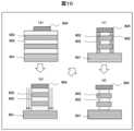
半導体デバイス、例えば、ゲルマニウム(Ge)をチャネル材料とするゲートオールアラウンド型電界効果トランジスタ(GAA型FET:Gate All Around type Field Effect Transistor)を製造する工程においては、シリコンゲルマニウム(SiGe)からなる犠牲層を、Geチャネル層に対して選択的に、均一性良く等方性エッチングする技術が求められると考えられる。そこで発明者等は、一例として、図10に示すような構造体を対象に従来の技術による原子層エッチングを行う場合について検討した。In the process of manufacturing a semiconductor device, for example, a gate all around type field effect transistor (GAA type FET) using germanium (Ge) as the channel material, a technology is required to selectively and uniformly isotropically etch a sacrificial layer made of silicon germanium (SiGe) with respect to the Ge channel layer. Therefore, the inventors have studied, as an example, the case of performing atomic layer etching by conventional technology on a structure such as that shown in FIG. 10.
図10は、処理対象の半導体ウエハ等の基板上の試料上に形成されGeチャネル層とSiGe犠牲層が交互に積層されて形成された所定の多層膜構造に従来の技術による原子層エッチングを施した場合の当該多層膜構造の変化を模式的に示す縦断面図である。本図10の(a)ないし(d)はエッチング処理が施されて変化する膜構造の形状の4段階の状態を示している。Figure 10 is a vertical cross-sectional view showing a schematic diagram of a multilayer structure formed by alternately stacking a Ge channel layer and a SiGe sacrificial layer on a sample on a substrate such as a semiconductor wafer to be processed, when the multilayer structure is subjected to atomic layer etching by a conventional technique. (a) to (d) of this figure show four stages of the shape of the film structure that changes when etching is performed.
図10の(a)は、下地構造901の上に、Geチャネル層902とSiGe犠牲層903が交互にエピタキシャル成長されており、処理対象でない部分を保護するマスク904が形成された構造であって、エッチング処理が開始されていない状態の膜構造を示す図である。図10の(b)は、図10の(a)の膜構造のGeチャネル層902とSiGe犠牲層903からなる多層構造を、塩素とアルゴンの混合ガスからなるプラズマを用いた反応性イオンエッチングにより、マスク904に覆われていない部分を異方的に加工した状態を示す図である。図10の(c)は、原子層エッチングの第一ステップとして、酸素プラズマを用いてGeチャネル層902とSiGe犠牲層903の側面を表面酸化させ、酸化物を主成分とする反応層905を形成した状態を示す図である。図10の(d)は、原子層エッチングの第二ステップとして、急速加熱を用いてGeチャネル層902とSiGe犠牲層903の表面に、酸化物を主成分とする反応層905を揮発させた状態を示す図である。Figure 10 (a) is a diagram showing a film structure in which a
発明者らの検討では、図10の(d)に示すように、Geチャネル層902とSiGe犠牲層903の積層構造において、SiGe犠牲層903のみを均一にエッチングしようとしたところ、Geに対して選択性を有するプロセスを用いていないために、SiGe犠牲層903だけでなく、エッチングせずに残すべきGeチャネル層902がエッチングされることが確認された。また、エッチング量が小さいことが好ましいGeチャネル層902のエッチング量は、SiGe犠牲層903のエッチング量よりも大きかった。この現象が生じる第一の原因は、まず図10の(c)に示すように、酸素プラズマによって生成する酸化物を主成分とする反応層905の厚みが、Ge組成の大きいGeチャネル層902で大きく、Ge組成の小さいSiGe犠牲層903で小さくなることがあげられる。これはGeの方が、Siと比較して酸化しやすいことに起因する。また、第二の原因は、Ge酸化物の揮発性がSi酸化物の揮発性よりも高いため、Ge組成の大きいGeチャネル層902に生じた酸化物を主成分とする反応層905が、加熱ステップにおいて揮発しやすいためである。この結果、従来の技術によるSiGe犠牲層903のエッチングでは、SiGe犠牲層903のエッチングと同時に、本来エッチング量を抑制するべきGeチャネル層902が大きくエッチングされてしまい、半導体デバイスの製造の歩留まりが著しく低下してしまう虞があった。In the study by the inventors, as shown in FIG. 10(d), in a stacked structure of a
このように、従来のプラズマを用いた原子層エッチング技術では、SiGe犠牲層903をエッチングする際に、Geチャネル層902をエッチングせずに残すことができない。このため従来のSiに対して選択的なSiGe原子層エッチング技術は、チャネル材料としてGeの適用が求められる次世代以降のデバイス製造工程においては、その適用が制限されると思われる。In this way, in the conventional atomic layer etching technique using plasma, when etching the SiGe
発明者等は、各種ガスのプラズマを用いてSiGeおよびGeの原子層エッチングを試みた。その結果、以下の事項(1)-(6)を見出した。The inventors have attempted atomic layer etching of SiGe and Ge using plasmas of various gases. As a result, they have found the following points (1)-(6).
(1)ウエハの温度を-40℃以上50℃未満の範囲として、SiGe膜およびGe膜の表面へ少なくともフッ素と水素と窒素を含有する混合ガスのプラズマから生成した活性種を供給することによって、その表面に窒素-水素(N-H)結合を含むことを特徴とするアンモニウム塩を主たる成分とする表面反応層が形成されること。(1) By setting the wafer temperature in the range of -40°C or higher and lower than 50°C, and supplying active species generated from a plasma of a mixed gas containing at least fluorine, hydrogen, and nitrogen to the surfaces of the SiGe film and the Ge film, a surface reaction layer is formed on the surface, the main component of which is an ammonium salt and characterized by containing nitrogen-hydrogen (N-H) bonds.
(2)混合ガスに酸素を添加した場合に、窒素-水素(N-H)結合を含むことを特徴とするアンモニウム塩の生成効率が高まること。(2) When oxygen is added to the mixed gas, the efficiency of producing ammonium salts, which are characterized by containing nitrogen-hydrogen (N-H) bonds, is increased.
(3)当該表面反応層の生成量は、Geの含有量が増えるにしたがい減少すること。(3) The amount of the surface reaction layer produced decreases as the Ge content increases.
(4)当該表面反応層の生成量は、プラズマ照射時間に対して自己飽和性(セルフリミティング性)を有すること。(4) The amount of the surface reaction layer produced is self-saturating (self-limiting) with respect to the plasma exposure time.
(5)当該表面反応層は50℃以上の加熱により除去されること。(5) The surface reaction layer is removed by heating to 50°C or higher.
(6)当該表面反応層の除去量は、加熱時間に対して自己飽和性(セルフリミティング性)を有すること。(6) The amount of the surface reaction layer removed is self-saturating (self-limiting) with respect to the heating time.
本発明はこの新たな知見((1)-(6))に基づいて生まれたものである。The present invention was born based on these new findings (1)-(6).
SiGeの原子層エッチング方法は、具体的には、以下の2つの工程1、工程2を実施する。Specifically, the SiGe atomic layer etching method involves the following two steps,
(工程1):少なくとも、四フッ化メタン(CF4)や三フッ化メタン(トリフルオロメタン:CHF3)や三フッ化窒素(NF3)や六フッ化硫黄(SF6)などのフッ素を含有するガスと、水素(H2)やジフルオロメタン(フッ化メチレン:CH2F2)やフルオロメタン(CH3F)やメタン(CH4)などの水素を含有するガスと、窒素(N2)や一酸化窒素(NO)やアンモニア(NH3)やNF3などの窒素を含有するガス、の混合ガスのプラズマを形成して、エッチング処理対象のSiGe膜の表面に、プラズマからフッ素、水素、窒素を含む反応性を有した粒子を供給し、当該SiGe膜の表面にN-H結合を含むことを特徴とするアンモニウム塩を主たる成分とする表面反応層を形成する工程。 (Step 1): A process for forming a plasma of a mixed gas of at least a fluorine-containing gas such as tetrafluoromethane (CF4 ), trifluoromethane (trifluoromethane:CHF3 ), nitrogen trifluoride (NF3 ), or sulfur hexafluoride (SF6 ), a hydrogen-containing gas such as hydrogen (H2 ), difluoromethane (methylenefluoride :CH2F2 ), fluoromethane (CH3F ), or methane (CH4 ), and a nitrogen-containing gas such as nitrogen (N2 ), nitric oxide (NO), ammonia (NH3 ), orNF3 , and supplying reactive particles containing fluorine, hydrogen, and nitrogen from the plasma to the surface of a SiGe film to be etched, thereby forming a surface reaction layer mainly composed of an ammonium salt characterized by containing an N-H bond on the surface of the SiGe film.
(工程2):工程1の次に、当該表面反応層を50℃以上に加熱することによって除去する工程(または、当該表面反応層を加熱によって脱離させる工程)。(Step 2): Following
そして、これら2つの工程1、工程2を一纏まりのサイクルとして、このサイクルを複数回繰り返すことにより、所望の量(膜厚)のSiGe膜のエッチングを実現する。Then, these two steps,
上記の構成によって、表面反応層の形成工程(工程1)および表面反応層の除去工程(工程2)が自己飽和性を持つことから、ウエハの面内方向および溝あるいは穴等の膜構造のパターンの深さ方向についてのエッチング量の均一性は高くなる。また、一回のサイクルで除去されるSiGe膜の量は高い精度で調節でき、サイクルを繰り返して得られるエッチングの量は繰り返すサイクルの回数によって調節できるため、積層されたSiGe膜をエッチングして形成する半導体デバイスの寸法精度を向上させることができる。With the above configuration, the surface reaction layer formation process (process 1) and the surface reaction layer removal process (process 2) are self-saturating, so the uniformity of the amount of etching in the in-plane direction of the wafer and in the depth direction of the film structure pattern such as a groove or hole is high. In addition, the amount of SiGe film removed in one cycle can be adjusted with high precision, and the amount of etching obtained by repeating the cycle can be adjusted by the number of repeated cycles, so that the dimensional precision of the semiconductor device formed by etching the stacked SiGe film can be improved.
図9は、処理対象の半導体ウエハ等の基板上の試料上に形成されGeチャネル層とSiGe犠牲層が交互に積層されて形成された所定の多層膜構造に本発明の技術による原子層エッチングを施した場合の当該多層膜構造の変化を模式的に示す縦断面図である。本図9の(a)ないし(d)はエッチング処理が施されて変化する膜構造の形状の4段階の状態を示している。Figure 9 is a vertical cross-sectional view showing the change in a multilayer structure formed by alternately stacking a Ge channel layer and a SiGe sacrificial layer on a sample on a substrate such as a semiconductor wafer to be processed, when the multilayer structure is subjected to atomic layer etching according to the technology of the present invention. (a) to (d) in Figure 9 show four stages of the shape of the film structure that changes when an etching process is performed.
図9の(a)は、下地構造901の上に、Geチャネル層902とSiGe犠牲層903が交互にエピタキシャル成長されており、処理対象でない部分を保護するマスク904が形成された構造であって、エッチング処理が開始されていない状態の膜構造を示す図である。図9の(b)は、図9の(a)の膜構造のGeチャネル層902とSiGe犠牲層903からなる多層構造を、塩素とアルゴンの混合ガスからなるプラズマを用いた反応性イオンエッチングにより、マスク904に覆われていない部分を異方的に加工した状態を示す図である。図9の(c)は、原子層エッチングの第一ステップとして、フッ素と水素と窒素を含有する混合ガスからなるプラズマを用いてGeチャネル層902とSiGe犠牲層903の側面の表面を処理し、主にSiGe層の表面に窒素-水素結合(N-H結合)を含むアンモニウム塩を主成分とする反応層906を形成した状態を示す図である。このときGeチャネル層902の表面にも図示しない微量のN-H結合を含むアンモニウム塩を主成分とする反応層が生成している。図9の(d)は、原子層エッチングの第二ステップとして、加熱を用いてGeチャネル層902とSiGe犠牲層903の表面に生成したN-H結合を含むアンモニウム塩を主成分とする反応層906を揮発させた状態を示す図である。9A is a diagram showing a film structure in which a
発明者らの検討では、図9の(d)に示すように、Geチャネル層902とSiGe犠牲層903の積層構造において、本発明の手順を用いてSiGe犠牲層903をエッチングしたところ、SiGe犠牲層903が、Geチャネル層902に対して選択的にエッチングされることが確認された。この現象が生じる第一の原因は、まず図9の(c)に示すように、フッ素と水素と窒素を含有する混合ガスのプラズマによって生成するアンモニウム塩を主成分とする反応層906の厚みが、Ge組成の小さいSiGe犠牲層903で大きく、Ge組成の大きいGeチャネル層902で極めて小さくなる(不図示)ことがあげられる。これはSiを多く含有する膜の方が、N-H結合を有するアンモニウム塩を成分とする反応層を生成しやすいという新たに見出された現象に起因する。また、第二の原因は、Geを含むアンモニウム塩の揮発性が、Siを含むアンモニウム塩の揮発性よりも高いため、Si組成の大きいSiGe犠牲層903に生じたアンモニウム塩を主成分とする反応層906が、加熱ステップにおいて揮発しやすいためである。この結果、本発明の技術によるSiGe犠牲層903のエッチングでは、SiGe犠牲層903のエッチングの際に、エッチングすべきでないGeチャネル層902のエッチング量は小さく、従来の技術を用いた場合と比較して、半導体デバイスの製造の歩留まりが大きく向上した。図9の(a)-(d)のより詳しい説明は、後述される図4の(a)-(c)の説明を参照できる。In the study by the inventors, as shown in (d) of FIG. 9, when the SiGe
なお、以下の実施例では、各工程が自己飽和性を持つ表面反応層の形成工程(工程1)と表面反応層の除去工程(工程2)とを含む一纏まりの工程を繰り返して行うエッチング処理を原子層エッチングと呼称する。本実施例において、「原子層」エッチングは1サイクル当たりのエッチング量が対象の膜を構成する物質の単一の原子から構成される層の厚さと同等であるという狭義の原子層エッチングに限定されない。例え1サイクル当たりのエッチングの量がナノメートルまたはこれ以上のオーダーであっても、各工程が処理の時間などに対して自己飽和的、すなわちセルフリミティングな傾向を有するものに対して当該処理を原子層エッチングとして呼称される。なお、「デジタルエッチング」、「セルフリミティング性サイクルエッチング」、「原子レベルエッチング」、「レイヤーバイレイヤーエッチング」等の呼称も同等の処理に対して用いることができる。In the following examples, an etching process in which a set of steps, each of which includes a self-saturating surface reaction layer formation step (step 1) and a surface reaction layer removal step (step 2), is repeated, is referred to as atomic layer etching. In this example, "atomic layer" etching is not limited to atomic layer etching in the narrow sense, in which the amount of etching per cycle is equivalent to the thickness of a layer composed of a single atom of the material that constitutes the target film. Even if the amount of etching per cycle is on the order of nanometers or more, the process is referred to as atomic layer etching if each step has a tendency to be self-saturating, i.e., self-limiting, with respect to the processing time. Note that terms such as "digital etching," "self-limiting cycle etching," "atomic level etching," and "layer-by-layer etching" can also be used for equivalent processes.
以下、本発明について、図面を用いて実施例を説明する。Below, the present invention is explained with reference to examples in the drawings.
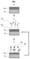
本発明の実施例について、図1乃至8を用いて以下に説明する。本実施例は、三フッ化メタン(CHF3)と酸素(O2)と窒素(N2)からなる混合ガスを用いて形成したプラズマにより処理対象のSiGe膜の表面に表面反応層を形成する工程を実施した後、赤外線ランプを用いたウエハ加熱により表面反応層を除去する工程を実施することで、シリコン等の半導体ウエハ上に予め形成された処理対象のSiGe膜を等方的に原子層エッチングするものを説明する。 An embodiment of the present invention will be described below with reference to Figures 1 to 8. This embodiment describes a process for forming a surface reaction layer on the surface of a SiGe film to be processed by plasma formed using a mixed gas of trifluoromethane (CHF3 ), oxygen (O2 ), and nitrogen (N2 ), and then performing a process for removing the surface reaction layer by heating the wafer using an infrared lamp, thereby isotropically etching an SiGe film to be processed that has been formed in advance on a semiconductor wafer such as silicon.
図1は、本発明の実施例に係るプラズマ処理装置の構成の概略を模式的に示す縦断面図である。Figure 1 is a vertical cross-sectional view showing a schematic outline of the configuration of a plasma processing apparatus according to an embodiment of the present invention.
プラズマ処理装置100の処理室1はベースチャンバー11により構成され、その中には被処理試料であるウエハ2(以下ウエハ2と記す)を戴置するためのウエハステージ4(以下、ステージ4と記す)が設置されている。プラズマ源には誘導結合放電(ICP:Inductively Coupled Plasma)方式を用いており、処理室1の上方には、石英チャンバー12とICPコイル34及び高周波電源20を備えたプラズマ源が設置されている。ここで、ICPコイル34は、石英チャンバー12の外側に設置されている。The
ICPコイル34にはプラズマ生成のための高周波電源20が整合器22を介して接続されている。高周波電力の周波数は13.56MHzなどの、数十MHzの周波数帯を用いるものとする。石英チャンバー12の上部には天板6が設置されている。天板6にはシャワープレート5が設置されており、その下部にはガス分散板17が設置されている。処理ガスはガス分散板17の外周から処理室1内に導入される。A high
処理ガスは、マスフローコントローラ制御部51内に配置されガス種毎に設置されたマスフローコントローラ50によって供給する流量が調整される。図1では、すくなくとも三フッ化メタン(CHF3)、酸素(O2)、窒素(N2)が処理ガスとして処理室1に供給され、これらガス(N2、O2、CHF3)の各々に対応してマスフローコントローラ50-1、50-2、50-3が備えられている。また、供給されるガスはこれらに限られない。なお、マスフローコントローラ制御部51には、後述の通りウエハ2裏面とこれが載置されるステージ4の誘電体膜上面との間に供給されるヘリウム(He)ガスの流量を調節するマスフローコントローラ50-4も含んで配置されている。 The flow rate of the process gas is adjusted by the
処理室1の下部は、処理室1内を減圧するため、真空排気配管16によって、排気手段15に接続されている。排気手段15は、例えば、ターボ分子ポンプやメカニカルブースターポンプやドライポンプで構成されるものとする。また、調圧手段14が排気手段15の上流側に設置されている。調圧手段14は、排気手段15の動作により処理室1内から排出される内部のガスやプラズマ10の粒子の流量を真空排気配管16の軸方向に垂直な面での断面積である流路断面積を増減させて調節して処理室1や放電領域3の圧力を調整するために、流路内に横切る方向に軸を有して配置され軸周りに回転する複数枚の板状のフラップや流路内部をその軸方向を横切って移動する板部材から構成されている。The lower part of the
ステージ4とICPプラズマ源を構成する石英チャンバー12との間には、ウエハ2を加熱するための赤外線ランプユニットが設置されている。赤外線ランプユニットは、主に赤外線ランプ62、赤外光を反射する反射板63、光透過窓74を備えている。赤外線ランプ62には円形状(リング状)のランプを用いる。なお、赤外線ランプ62から放射される光は、可視光から赤外光領域の光を主とする光を放出するものとする。ここではこのような光を赤外光と呼ぶ。図1に示した構成では、赤外線ランプ62として3周分の赤外線ランプ62-1、62-2、62-3が設置されているものとしたが、2周、4周などとしてもよい。赤外線ランプ62の上方には赤外光を下方に向けて反射するための反射板63が設置されている。Between the
赤外線ランプ62には赤外線ランプ用電源64が接続されており、その途中には、高周波電源20で発生するプラズマ生成用の高周波電力のノイズが赤外線ランプ用電源64に流入しないようにするための高周波カットフィルタ25が設置されている。また、赤外線ランプ62-1、62-2、62-3に供給する電力を、互いに独立に制御できるような機能が赤外線ランプ用電源64には付けられており、ウエハ2の加熱量の径方向分布を調節できるようになっている。An infrared
赤外線ランプユニットの中央には、マスフローコントローラ50から石英チャンバー12の内部に供給されたガスを処理室1の側に流すための、ガスの流路75が形成されている。そして、このガスの流路75には、石英チャンバー12の内部で発生させたプラズマ中で生成されたイオンや電子を遮蔽し、中性のガスや中性のラジカルのみを透過させてウエハ2に照射するための、複数の穴の開いたスリット板(イオン遮蔽板)78が設置されている。A
ステージ4には、ステージ4を冷却するための冷媒の流路39がその内部に形成されており、チラー38によって冷媒が循環供給されるようになっている。また、ウエハ2を静電吸着によってステージ4に固定するため、板状の電極板である静電吸着用電極30がステージ4に埋め込まれており、それぞれに静電吸着用のDC(Direct Current:直流)電源31が接続されている。The
また、ウエハ2を効率よく冷却するため、ステージ4に載置されたウエハ2の裏面とステージ4との間にHeガスを供給できるようになっている。また、静電吸着用電極30を作動させてウエハ2を静電吸着したまま加熱や冷却を行っても、ウエハ2の裏面に傷がつかないようにするため、ステージ4のウエハ戴置面はポリイミド等の樹脂でコーティングされている。またステージ4の内部には、ステージ4の温度を測定するための熱電対70が設置されており、この熱電対70は熱電対温度計71に接続されている。In order to efficiently cool the
また、ウエハ2の温度を測定するための光ファイバー92-1、92-2が、ステージ4に載置されたウエハ2の中心部付近(ウエハ中心とも称す)、ウエハ2の径方向ミドル付近(ウエハミドルとも称す)、ウエハ2の外周付近(ウエハ外周とも称す)、の3箇所に設置されている。光ファイバー92-1は、外部赤外光源93からの赤外光をウエハ2の裏面にまで導いてウエハ2の裏面に照射する。一方、光ファイバー92-2は、光ファイバー92-1により照射された赤外光のうちウエハ2を透過・反射したIR光を集めて分光器96へ伝送する。In addition, optical fibers 92-1 and 92-2 for measuring the temperature of the
外部赤外光源93で生成された外部赤外光は、光路をオン/オフさせるための光路スイッチ94へ伝送される。その後、光分配器95で複数に分岐し(図1の場合は3つに分岐)、3系統の光ファイバー92-1を介してウエハ2の裏面側のそれぞれの位置に照射される。The external infrared light generated by the external infrared
ウエハ2で吸収・反射された赤外光は光ファイバー92-2によって分光器96へ伝送され、検出器97でスペクトル強度の波長依存性のデータを得る。そして得られたスペクトル強度の波長依存性のデータは制御部40の演算部41に送られて、吸収波長が算出され、これを基準にウエハ2の温度を求めることができる。また、光ファイバー92-2の途中には光マルチプレクサー98が設置されており、分光計測する光について、ウエハ中心、ウエハミドル、ウエハ外周のどの計測点における光を分光計測するかを切り替えられるようになっている。これにより演算部41では、ウエハ中心、ウエハミドル、ウエハ外周ごとのそれぞれの温度を求めることができる。The infrared light absorbed and reflected by the
図1において、60は石英チャンバー12を覆う容器であり、81はステージ4とベースチャンバー11の底面との間で真空封止するためのOリングである。In Figure 1, 60 is a container covering the
制御部40は、高周波電源20からICPコイル34への高周波電力供給のオン/オフを制御する。また、集積マスフローコントローラ制御部51を制御して、それぞれのマスフローコントローラ50から石英チャンバー12の内部へ供給するガスの種類及び流量を調整する。この状態で制御部40は更に排気手段15を作動させると共に調圧手段14を制御して、処理室1の内部が所望の圧力となるように調整する。The
更に、制御部40は、静電吸着用のDC電源31を作動させてウエハ2をステージ4に静電吸着させ、Heガスをウエハ2とステージ4との間に供給するマスフローコントローラ50-4を作動させた状態で、熱電対温度計71で測定したステージ4の内部の温度、及び検出器97で計測したウエハ2の中心部付近、半径方向ミドル部付近、外周付近のスペクトル強度情報に基づいて演算部41で求めたウエハ2の温度分布情報に基づいて、ウエハ2の温度が所定の温度範囲になるように赤外線ランプ用電源64、チラー38を制御する。Furthermore, the
図2を用いて、本実施例のプラズマ処理装置100で実施されるウエハ2の処理の流れについて説明する。図2は、本発明の実施例に係るプラズマ処理装置100の実施するウエハ上に予め形成されたSiGeを含む膜のエッチング処理の流れの概略を示すフローチャートである。The flow of processing the
本図2において、ウエハ2の処理を開始する前に、表面にSiGe膜を含む処理対象の膜層を含む膜構造が予め配置されたウエハ2が、処理室1内のステージ4上に載置され、DC電源31からの直流電力が静電吸着電極30に供給されて形成された静電気力によってステージ4上に保持される。In FIG. 2, before processing of the
処理の開始後、ステップS201では、処理室1内に少なくともフッ素と水素と窒素を含有するガスが導入される。ここでフッ素と水素と窒素を含有するガスとしては、本実施例で説明する三フッ化メタン(CHF3)/酸素(O2)/窒素(N2)からなる混合ガス以外にも、例えば4フッ化メタン(CF4)/水素(H2)/酸化窒素(NO)や、四フッ化メタン(CF4)/アンモニア(NH3)や、三フッ化窒素(NF3)/水素(H2)や、二フッ化メタン(CH2F2)/酸素(O2)/窒素(N2)などの様々な混合ガスを利用できる。また、これらのガスをアルゴン(Ar)や窒素(N2)などで希釈した混合ガスを利用しても良い。また、本ステップS201におけるウエハ温度は、ウエハ2が載置されているステージ4の温度調節機能によって一定に保たれている。なお、ここで酸素を混合する場合があるが、酸素を混合することは、三フッ化メタンなどが酸素により酸化されて、反応を促進するフッ素を放出する効果や、酸素が水素と結合して生じるH2Oがアンモニウム塩の生成を促進することなどにより、N-H結合を有することを特徴とするアンモニウム塩を主成分とする反応層の生成効率を高める効果がある。 After the start of the process, in step S201, a gas containing at least fluorine, hydrogen, and nitrogen is introduced into the
次に、ステップS202では、放電領域3内部に上記ガスを用いてプラズマ10が生成され、プラズマ10中のフッ素と水素と窒素を含むガスの原子または分子が活性化されて生成されたフルオロカーボンラジカル(CFx)やフッ化水素(HF)などの反応性粒子(活性種とも言う)が生成される。また、ステップS203では、反応性粒子が、ガス流路75およびスリット板78の貫通孔を通してウエハ2の表面に供給され、SiGe膜を含む膜層の表面に付着する。反応性を有した粒子は付着した膜層の表面の材料と反応してプラズマ10の生成の条件やステージ4の温度等の処理の条件によって定まる厚さの表面反応層が形成される。プラズマを照射する際のウエハステージ4の温度は、50℃未満が好ましい。好適な温度範囲は-40℃から50℃の範囲である。これは、このときウエハ2の温度が50℃以上になると、反応生成物の脱離が進むため、プラズマ照射中にエッチングが進行してしまい、反応のセルフリミティング性が低下するからである。このときSiGe膜やGe膜上に生成する表面反応層は、窒素-水素(N-H)結合が含まれていることが大きな特徴である。この表面反応層は、少なくともN-H結合を有しており、(NH4)xSiFyや(NH4)xGeFyなどのアンモニウム塩が構成成分として含まれる。 Next, in step S202,
その後、ステップS204では、所定の厚さの表面反応層が形成されたことが膜厚の検出器(不図示)により或いは予め定められた時間の経過の確認等により制御部40によって確認された後、調圧手段14が真空排気配管16の流路断面積を大きくして排気量を増大させ、処理室1内部を大きく減圧させる。そして、処理室1内に供給されたフッ素と水素と窒素を含むガスが速やかに排気される。このことにより表面反応層の形成処理が終了する。この際、処理室1内のフッ素と水素と窒素を含むガスを置換するように、Ar等の不活性ガスを処理室1内部に供給して、フッ素と水素と窒素を含むガスの排出を促進させても良い。Then, in step S204, after the
次に、ステップS205では、赤外線ランプ62を点灯し、赤外線ランプ62から放射される光(赤外光)によりウエハ2の表面を真空状態で加熱する。このときの赤外光によるウエハ2の加熱温度は、50℃以上であることが好ましく、好適な温度範囲は、50℃から300℃である。真空加熱時の処理室1の圧力は100 Pa以下が好ましい。ウエハ2の温度は、赤外線ランプの照射時間の増大に伴って例えば約10℃/秒の速度で上昇し、この温度上昇により、表面反応層が表面から揮発して、膜層の表面から除去される(脱離される)。ウエハ2の温度が所定の温度に上昇したことが温度の検出機構(92-97、41)により確認されるかあるいは制御部40によって予め定められた時間の経過が確認された後、赤外線ランプ62は消灯される。Next, in step S205, the
揮発する反応生成物の例としては、例えばアンモニウム塩が分解することにより生じる、四フッ化ケイ素(SiF4)や、四フッ化ゲルマニウム(GeF4)、アンモニア(NH3)、フッ化水素(HF)などが挙げられる。ウエハ2から脱離したこれらの反応生成物の粒子は、調圧手段14あるいは排気手段15の動作による処理室1内部の排気の動作またはこれによって生じている処理室1内部の粒子の移動の流れによって処理室1内部から処理室1外部へ排出される。続いて、ステップS206において処理室1内部から反応生成物を含むガスが処理室1外部へ排気される。 Examples of volatilized reaction products include silicon tetrafluoride (SiF4 ), germanium tetrafluoride (GeF4 ), ammonia (NH3 ), hydrogen fluoride (HF), etc., which are generated by decomposition of ammonium salt. These reaction product particles desorbed from
上記のステップS201乃至S206を一纏まりとした1サイクルが終了する。当該サイクルによってプラズマとの反応でSiGe膜の表面に生じた表面反応層が除去(脱離)されるために、SiGe膜が表面反応層の膜層の厚さの分だけ除去され、SiGe膜の膜厚が小さくされる。Ge膜の場合は、SiGe膜の場合よりも生成量は小さいが、N-H結合を含有する表面反応層が生成する。このため、Geのエッチングもわずかに進む。したがって、膜構造がSiGeとGeの多層構造を有する場合には、SiGeのエッチングが選択的に進み、Geのエッチング量は少ない。このSiGeのエッチング量とGeのエッチング量が選択比である。また、このときのSiGe膜厚の変化量が、1サイクル当たりのエッチング量である。One cycle consisting of the above steps S201 to S206 is completed. The surface reaction layer generated on the surface of the SiGe film by the reaction with the plasma is removed (desorbed) by this cycle, so the SiGe film is removed by the thickness of the film layer of the surface reaction layer, and the film thickness of the SiGe film is reduced. In the case of a Ge film, the amount of generation is smaller than that of a SiGe film, but a surface reaction layer containing N-H bonds is generated. Therefore, etching of Ge also progresses slightly. Therefore, when the film structure has a multilayer structure of SiGe and Ge, etching of SiGe progresses selectively, and the etching amount of Ge is small. The etching amount of SiGe and the etching amount of Ge are the selectivity ratio. The change in the SiGe film thickness at this time is the etching amount per cycle.
この後、制御器40において、図示しない膜厚検出器からの出力を受信してこれから得られた結果から所望のエッチング量の到達の有無、或いは予めのテスト等から所望のエッチング量が得られることが導出された上記サイクルの実施の回数を含む終了の条件が満たされたかが判定される(ステップS207)。条件を満たすと判定された場合(S207:はい)には、SiGe膜を含む膜層のエッチング処理を終了し、満たしていないと判定された場合(S207:いいえ)には、ステップS201に戻り、再度サイクル(S201-S206)を実施する。このように本実施例では、所望のエッチング量が得られるまで上記サイクル(S201-S206)が繰り返して実施される。After this, the
以下、本実施例のプラズマ処理装置100を用いたウエハ2上のSiGe膜を含む膜層のエッチングを、反応層形成用のガスとしてCHF3/O2/N2を用いて実施する場合について、動作の順序を図3、4を用いて説明する。図3は、図1に示す実施例に係るウエハの処理中の処理の条件に含まれる複数のパラメータの時間の経過に伴う変化を示すタイムチャートである。図3において、パラメータは、上から順にガス供給流量、高周波電源電力、赤外線ランプ電力、静電吸着、ウエハ表面温度が示されている。 The sequence of operations for etching a film layer including a SiGe film on a
図4は、図3に示す実施例に係るウエハの処理中におけるSiGe膜を含む膜層を含む膜構造の変化の概略を模式的に示す断面図である。特に、図4では、ウエハ2の下地膜401上にSiGe膜402が境を接して積層されて配置された膜構造のSiGe膜402の表面付近の構造とその変化が模式的に示されている。Figure 4 is a cross-sectional view showing a schematic overview of changes in a film structure including a film layer including a SiGe film during processing of a wafer according to the embodiment shown in Figure 3. In particular, Figure 4 shows a schematic view of the structure and changes near the surface of the
まず、図3に示す処理中の時刻t0において、制御部40からの指令信号に応じて、処理室1に設けられた搬送口(図示省略)を介して、図4の(a)に示される下地膜401とエッチングの処理対象の膜層とされるSiGe膜402とを備えた膜構造が予め形成されたウエハ2が処理室1内部へ搬入されてステージ4に載置される。その後にDC電源31からの電力が静電吸着電極30に供給されウエハ2がステージ4上の誘電体膜上に静電吸着され保持される。さらに、制御部40からの指令信号に応じてマスフローコントローラ制御部51のHeガス対応のマスフローコントローラ50-4によりウエハ2の裏面とステージ4との間の隙間に供給されるウエハ冷却用のHeガスの流量が調節されて供給され、当該隙間のHeガスの圧力が所定の範囲内の値に調節される。この結果、ステージ4とウエハ2との間の熱伝達が促進され、ウエハ2の温度が予めチラー38により所定の温度にされた冷媒が冷媒の流路39に供給されて循環するステージ4の温度に近い値T1にされる。First, at time t0 during processing shown in FIG. 3, in response to a command signal from the
次に、図3に示す時刻t1において、制御部40からの指令信号に応じて、マスフローコントローラ50のCHF3用のマスフローコントローラ50-3、O2用のマスフローコントローラ50-2、N2用のマスフローコントローラ50-1の各々で供給される流量が調節されてこれら複数の種類の物質のガスが混合された混合ガスが処理用のガスとして処理室1内に予め定められた範囲内の流量で供給される。これと共に、調圧手段14の開度が調節されて処理室1の内部および石英チャンバー12の内部の放電領域3内の圧力が所期の範囲内の値にされる。 3, the flow rates of theCHF3 mass flow controller 50-3, theO2 mass flow controller 50-2, and theN2 mass flow controller 50-1 of the
この状態で、図3に示す時刻t2において、制御部40からの指令信号に応じて高周波電源20からの所定の値Wの高周波電力がICPコイル34に供給され、石英チャンバー12の内部の放電領域3内にプラズマ放電が開始され、石英チャンバー12の内部にプラズマ10が生起される。この際、プラズマ10の生成されている間のウエハ2の温度をプラズマ10の生成前と同等に保つため赤外線ランプ62へ電力は供給されていない。3, a predetermined value W of high frequency power is supplied from the high
この状態で、CHF3/O2/N2ガスの粒子の少なくとも一部がプラズマ10にて励起、解離あるいは電離化され、イオン等荷電粒子または活性種等の反応性粒子が形成される。放電領域3において形成された活性種等の反応性粒子および中性のガスはスリット板78に形成されたスリットまたは貫通孔を通過して処理室1に導入されてウエハ2表面に供給される。図4の(b)に示されるように、フルオロカーボンラジカル(CFx)やHFなどを含む活性種403はウエハ2のSiGe膜402の表面に吸着しSiGe膜402の材料と相互作用を起こし、表面反応層404が形成される。つまり、SiGe膜402の膜層の表面にフッ素、水素、窒素を含む反応性の粒子403を供給してSiGe膜402の膜層の表面に表面反応層404を形成する。 In this state, at least a part of the particles of the CHF3 /O2 /N2 gas is excited, dissociated or ionized in the
この表面反応層404は、少なくともN-H結合を主たる成分として含有する反応生成物であり、アルミニウムのKα線を用いてX線光電子分光法で測定した場合に、窒素1sスペクトルの結合エネルギーが、402±2eV付近にピークを持つことが大きな特徴である。また、この反応層にはGe-F結合や、Si-F結合も含まれ、(NH4)xSiFyや(NH4)xGeFyなどの化学組成で示されるアンモニウム塩が含まれていることを特徴とする。図5は、表面反応層404を形成したSiGe膜402の表面を、アルミニウムのKα線を用いたX線光電子分光法で分析した場合の、光電子スペクトルである。結合エネルギー402±2eV付近に、N-H結合の存在を示す、表面反応層404に起因するピークが観測されている。この表面反応層404の組成は、用いるガスの組成や反応時間に依存して、単体の水素、単体のフッ素、あるいはNH3、アンモニウム塩など、水素、窒素、フッ素、SiGeの各種の結合状態が混じりあった状態となる場合や、添加した酸素ガスなどに起因する、酸素が含まれる場合もある。なお、ここに示した結合エネルギーの値は、初期サンプルの表面に観測される表面汚染炭素に起因する炭素1sピークの位置が284.5eVであるとして校正した値である。 This
図6は、表面反応層404に起因する結合エネルギー402±2eVのピーク強度の、プラズマ処理時間に対する依存性を示すグラフである。プラズマ処理時間とは、高周波電力を供給し始めてからの経過時間を示す。図6に示す通り、表面反応層404に起因する結合エネルギー402±2eVのピーク強度は、プラズマ処理時間の経過に伴い増大して飽和傾向を示し、プラズマ処理時間が3分以上でほぼ一定となった。このように、反応生成物の生成量が自己飽和性を持つ性質は、金属表面やシリコン表面の自然酸化現象とよく似ている。このように、表面反応層404の形成に自己飽和性があるために、飽和に要する時間以上のプラズマ処理をすることで、一サイクル当たりに生成する表面反応層404の量を一定にすることができる。また、このプラズマ照射中にはSiGe層のエッチングが進んでいないことが確認されている。これは、表面に生成する反応層がエッチングの進行を阻害する性質があるためである。このように、プラズマ照射中にエッチングが進行しないため、エッチング量は、プラズマ処理時間に対してセルフリミティング性をもつ表面反応層404の生成量で決まることになる。このため、プラズマ処理の時間が飽和に要する時間以上であれば、エッチング量はプラズマ処理時間に全く依存せず、サイクル数で決まることになる。なお、本実施例で示した実験条件では、表面反応層404の生成量が飽和するまでに3分を要したが、プラズマ源(12、34)とウエハ2の距離や基板温度などの装置パラメータに応じて、飽和までに要する時間は変化する。例えばプラズマ源とウエハ2の距離を短くすることで、飽和までに要する時間を短縮することが可能である。Figure 6 is a graph showing the dependency of the peak intensity of the
表面反応層404の生成が飽和するために必要なプラズマ処理時間が経過した後は、図3に示す時刻t3において、制御部40からの指令信号に応じて、高周波電源20からの高周波電力の出力が停止されると共に放電領域3への処理ガスの供給が停止される。このことにより、放電領域3内でのプラズマ10が消失される。また、時刻t3から時刻t4の間に、処理室1内の処理ガスや反応性粒子等の粒子は調圧手段14で開度が調節された真空排気配管16および排気手段15を介して処理室1の外部に排気される。After the plasma processing time required for the generation of the
時刻t4において、制御部40からの指令信号に応じて赤外線ランプ62を点灯し、図4の(c)に示すように、赤外線ランプ62から放射される光(赤外光)405によりウエハ2の表面を真空加熱する。赤外線ランプの照射時間は例えば15秒とした。ウエハ2表面の最大到達温度は50から300℃の範囲が適している。この工程は、表面反応層404を、四フッ化シリコンや四フッ化ゲルマニウム、アンモニア、フッ化水素などの反応生成物406に分解して揮発または脱離させる反応である。この脱離反応は、高温で低圧なほど高速に進む。発明者らは、この脱離反応を起こすためには、ウエハ2の表面の温度は50℃以上が必要であり、かつ処理室1の圧力は100Pa以下が好適であることを見出した。At time t4, the
図7は、低温で表面反応層404を生成した後、温度25℃、50℃、75℃、100℃、125℃、150℃と変化させながら等時間アニールした場合の、表面反応層404の残存量を、照射直後における結合エネルギー402±2eVのピーク強度を1として、その変化をプロットしたものである。この結果、表面反応層404は、25℃のアニール処理では強度に変化がないが、50℃以上の加熱において強度が減少を始めることが分かる。このことから、表面反応層404を除去するために好適な加熱温度は、50℃以上であることを見出した。Figure 7 plots the change in the remaining amount of
また、ランプ加熱に必要な時間は、典型的には、10秒から30秒であるが、この加熱時間はランプ62のパワーや、ランプ62とウエハ2の距離などにより変化するものである。この加熱工程では、ウエハ2の表面に生成した表面反応層404のみが分解して揮発し、表面反応層404の下部に存在する未反応のSiGe膜402は全く変化しないので、表面反応層404部分のみを除去することができる。すなわち、表面反応層404の除去量は、ランプ加熱時間がそれを除去する時間以上であって十分であれば、ランプ加熱時間に依存しない。従って、表面反応層404を形成する工程に加えて、表面反応層404を除去する工程も、除去量がランプ加熱時間に依存しないという意味で、セルフリミティング性をもつ。このように、本発明のSiGe膜の原子層エッチングでは、プラズマ照射時間、およびランプ加熱時間が、それぞれ飽和に要する時間を超えて十分確保されていれば、エッチング量はプラズマ照射時間やランプ加熱時間に依存せず、プラズマ照射とランプ加熱のサイクル数で決まることになる。このため、エッチング量のウエハ2面内やパターン深さによらず一定になるのである。The time required for lamp heating is typically 10 to 30 seconds, but this heating time varies depending on the power of the
なお、この加熱工程に際しては、ウエハ2はウエハステージ4上に戴置された状態であるが、ウエハ2の裏面の熱伝導を高めるために用いられるヘリウムガスの供給は停止し、ウエハ2の表面の温度が速やかに上昇するようにした。なお、本実施の形態ではウエハ2をウエハステージ4上に戴置したままの状態で処理したが、リフトピン(不図示)などを用いてウエハ2がウエハステージ4と熱的に接触していない状態で赤外光を照射しても良い。表面反応層404を除去するために必要な加熱時間が経過した後は、赤外線ランプ62が消灯されて、処理室1の残留ガスが排気手段15を用いて処理室1外部へ排気される。その後、ヘリウムガスの供給が再開されてウエハ2とウエハステージ4の熱伝導が高められ、ウエハ2の温度は、チラー38によって-40から40℃の範囲の所定の温度に冷却され、1サイクル目の処理が終了した。During this heating process, the
制御部40からの指令信号に応じて、図3に示す時刻t5において、赤外線ランプ62を消灯する。また、処理室1内の反応生成物の粒子などを含むガスは、調圧手段14で開度が調節された真空排気配管16および排気手段15を介して処理室1外部に排気される。さらに、時刻t5以降の時間で、図2において説明の通り、ウエハ2上のSiGe膜402のエッチング量あるいは残り膜厚さが所望の値に到達したか判定され(ステップS207に対応)、判定結果に応じて次のサイクルの開始(S201-S206)またはウエハ2の処理の終了の工程が行われる。In response to a command signal from the
次のサイクルを開始する場合は、時刻t5以降の任意の時刻t6において、制御部40からの指令信号に応じて、時刻t1からの動作と同様にCHF3/O2/N2ガスの放電領域3への導入が開始される。つまり、次のサイクルとして、再度、図4の(b)で説明した表面反応層404の形成工程と、図4の(C)で説明した表面反応層を加熱によって脱離させる工程と、を実施する。ウエハ2の処理を終了する場合は、時刻t6においてウエハ2の裏面とステージ4上面との間の隙間に供給されていたHeガスの供給を停止するとともに、バルブ52を開いて当該隙間からHeガスを排出して隙間内の圧力を処理室1内の圧力と同程度にするとともに、静電気の除去を含むウエハ2の静電吸着の解除の工程を実施する。以上でSiGe膜402のエッチング処理の工程を終了する。 When the next cycle is to be started, at any time t6 after time t5, in response to a command signal from the
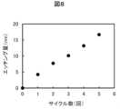
本実施例において、10nmのエッチング量が必要な場合には、上記のサイクルを3回繰り返してエッチングを終了した。図8は、図1に示す本実施例に係るプラズマ処理装置100が実施したエッチング処理においてサイクル数とエッチングの量との関係を示すグラフである。本図8は、横軸にサイクルの回数を採り、縦軸に実施された各サイクル終了後で次のサイクルの開始前にIn-Situエリプソメトリ(偏光解析法)を用いて検出したエッチング量(エッチングの深さ)を示したものである。In this embodiment, when an etching amount of 10 nm was required, the above cycle was repeated three times to complete the etching. Figure 8 is a graph showing the relationship between the number of cycles and the amount of etching in the etching process performed by the
本図8に示す通り、本例ではサイクルの回数の増加に伴ってほぼ線形にエッチング量が変化している。この図8から、本実施例におけるSiGe膜の1サイクル当たりのエッチング量は、例えば、3.3nm/サイクルであることが判った。As shown in Figure 8, in this example, the amount of etching changes almost linearly with an increase in the number of cycles. From Figure 8, it was found that the amount of etching per cycle of the SiGe film in this example was, for example, 3.3 nm/cycle.
以上の通り、本実施例の表面反応層404を形成する第1の工程と表面反応層404を除去する第2の工程は、共に自己飽和的に終了する性質を持つ。このことから、本実施例において、回路パターンを有する膜構造が予め形成されたウエハ2をエッチングした場合の、一回のサイクルを終えた際のSiGe膜402表面のエッチング量はウエハ2の面内方向および深さ方向についてバラつきが低減されより均一に近づけることができる。As described above, in this embodiment, the first process of forming the
上記の自己飽和性を利用していることから、ウエハ2上面の水平方向や深さ方向の位置によってウエハ2に供給される反応性粒子の密度が異なる分布を有した場合でも、エッチング量が必要以上に大きくなったり不足したりすることが抑制され、エッチング量のバラつきが低減される。また、全体のエッチング量は上記第1および第2の工程を含む1つのサイクルの繰り返す回数の増減で調節することができ、本実施例の当該エッチング量は1サイクル当たりのエッチング量を回数倍または回数分の和となる。結果として、本実施例では、従来の連続的なプラズマ処理によるエッチングと比較して、エッチング処理による加工後の寸法の制御性さらには処理の歩留まりを向上させることができる。Because the above-mentioned self-saturation property is utilized, even if the density of reactive particles supplied to the
以上本実施例によれば、SiGe膜を、ウエハ面内方向やパターン深さ方向において高い均一性で加工する、等方性原子層エッチング技術を提供することができる。なお、SiGe膜のエッチング量はGe膜のエッチング量と比較して大きいため、本発明はSiGe膜のGe膜に対する選択的なエッチングに好適である。一方、混合ガスの種類や混合比、あるいはステージ温度などの装置パラメータによって、Ge膜のエッチング量は変化する。Geの原子層エッチングが必要なアプリケーションでは、Geの表面にN-H結合を含むことを特徴とする表面反応層を形成する本発明の技術を、Ge膜の原子層エッチングとして適用することも可能である。According to the present embodiment, it is possible to provide an isotropic atomic layer etching technique that processes a SiGe film with high uniformity in the wafer in-plane direction and the pattern depth direction. Since the etching amount of a SiGe film is larger than that of a Ge film, the present invention is suitable for selective etching of a SiGe film relative to a Ge film. On the other hand, the etching amount of a Ge film varies depending on the type and mixture ratio of the mixed gas, or the equipment parameters such as the stage temperature. In applications requiring atomic layer etching of Ge, the technique of the present invention that forms a surface reaction layer characterized by containing N-H bonds on the surface of Ge can also be applied as atomic layer etching of a Ge film.
なお、上記図1のプラズマ処理装置100においては、赤外線ランプ62を放電領域3を囲む石英チャンバー12の外周の処理室1上方の真空容器外部に配置したが、石英チャンバー12または真空容器の内部に配置しても良い。また、上記した例は本発明を分かりやすく説明するために詳細に説明したものであり、必ずしも説明した全ての構成を備えるものに限定されるものではない。1, the
1…処理室、2…ウエハ、3…放電領域、4…ステージ、5…シャワープレート、6…天板、10…プラズマ、11…ベースチャンバー、12…石英チャンバー、14…調圧手段、15…排気手段、16…真空排気配管、17…ガス分散板、20…高周波電源、22…整合器、25…高周波カットフィルタ、30…静電吸着用電極、31…DC電源、34…ICPコイル、38…チラー、39…冷媒の流路、40…制御部、41…演算部、50…マスフローコントローラ、51…マスフローコントローラ制御部、52・・バルブ、60…容器、62…赤外線ランプ、63…反射板、64…赤外線ランプ用電源、70…熱電対、71…熱電対温度計、74…光透過窓、75…ガスの流路、78…スリット板、81…Oリング、92…光ファイバー、93…外部赤外光源、94…光路スイッチ、95…光分配器、96…分光器、97…検出器、98…光マルチプレクサー、100…プラズマ処理装置、401…下地膜、402…SiGe膜、403…活性種、404…表面反応層、406…反応生成物、901…下地構造、902…Geチャネル層、903…SiGe犠牲層、904…マスク、905…酸化物を主成分とする反応層、906…アンモニウム塩を主成分とする反応層。1...Processing chamber, 2...Wafer, 3...Discharge area, 4...Stage, 5...Shower plate, 6...Top plate, 10...Plasma, 11...Base chamber, 12...Quartz chamber, 14...Pressure adjustment means, 15...Exhaust means, 16...Vacuum exhaust piping, 17...Gas dispersion plate, 20...High frequency power source, 22...Matcher, 25...High frequency cut filter, 30...Electrostatic adsorption electrode, 31...DC power source, 34...ICP coil, 38...Chiller, 39...Refrigerant flow path, 40...Control unit, 41...Calculation unit, 50...Mass flow controller, 51...Mass flow controller control unit, 52...Valve, 60...Container, 62...Infrared lamp, 63...Reflector, 64... Power supply for infrared lamp, 70...thermocouple, 71...thermocouple thermometer, 74...light-transmitting window, 75...gas flow path, 78...slit plate, 81...O-ring, 92...optical fiber, 93...external infrared light source, 94...optical path switch, 95...optical distributor, 96...spectroscope, 97...detector, 98...optical multiplexer, 100...plasma processing apparatus, 401...underlying film, 402...SiGe film, 403...active species, 404...surface reaction layer, 406...reaction product, 901...underlying structure, 902...Ge channel layer, 903...SiGe sacrificial layer, 904...mask, 905...reaction layer mainly composed of oxide, 906...reaction layer mainly composed of ammonium salt.
Claims (6)
Translated fromJapanese前記膜層の表面に、少なくともフッ素、水素、窒素を含む混合ガスのプラズマを用いて反応性の粒子を供給して、前記膜層の表面に窒素-水素結合を含有する反応層を形成する工程と、
前記膜層を加熱して前記反応層を脱離させる工程と、
を備え、
前記膜層は、Ge層とSiGe層とが交互に積層されて形成された所定の多層膜を含み、
前記Ge層は、GAA型FETのチャネル層を構成する、エッチング方法。 1. A method for etching a semiconductor-containing film layer to be processed disposed on a surface of a wafer, comprising:
a step of supplying reactive particles to the surface of the film layer using plasma of a mixed gas containing at least fluorine, hydrogen, and nitrogen to form a reaction layer containing nitrogen-hydrogen bonds on the surface of the film layer;
heating the membrane layer to desorb the reaction layer;
Equipped with
the film layer includes a predetermined multilayer film formed by alternately stacking Ge layers and SiGe layers;
The Ge layer constitutes a channel layer of a GAA type FET.
前記混合ガスは少なくともフッ素、水素、窒素、酸素を含む、エッチング方法。 2. The etching method according to claim 1,
The etching method, wherein the mixed gas contains at least fluorine, hydrogen, nitrogen, and oxygen.
前記窒素-水素結合を含有する反応層がアンモニウム塩を含む、エッチング方法。 The etching method according to any one of claims 1 to 2,
The etching method, wherein the reaction layer containing nitrogen-hydrogen bonds comprises an ammonium salt.
前記半導体がSiGeまたはGeである、エッチング方法。 The etching method according to any one of claims 1 to 3,
The etching method, wherein the semiconductor is SiGe or Ge.
前記反応層が、前記反応層を形成する工程の処理時間および前記反応層を脱離させる工程の処理時間に対してセルフリミティング性を有する、エッチング方法。 5. The etching method according to claim 1, further comprising the steps of:
An etching method, wherein the reaction layer has a self-limiting property with respect to a processing time of the step of forming the reaction layer and a processing time of the step of removing the reaction layer.
前記反応層を形成する工程と前記反応層を脱離させる工程とを含んだ複数の工程を一纏まりのサイクルとして、前記サイクルを複数回繰り返す、エッチング方法。 6. The etching method according to claim 1 ,
an etching method comprising: a cycle including a step of forming the reaction layer and a step of removing the reaction layer; and repeating the cycle a number of times.
Applications Claiming Priority (1)
| Application Number | Priority Date | Filing Date | Title |
|---|---|---|---|
| PCT/JP2022/003711WO2023148797A1 (en) | 2022-02-01 | 2022-02-01 | Etching method |
Publications (2)
| Publication Number | Publication Date |
|---|---|
| JPWO2023148797A1 JPWO2023148797A1 (en) | 2023-08-10 |
| JP7535175B2true JP7535175B2 (en) | 2024-08-15 |
Family
ID=87553304
Family Applications (1)
| Application Number | Title | Priority Date | Filing Date |
|---|---|---|---|
| JP2023511863AActiveJP7535175B2 (en) | 2022-02-01 | 2022-02-01 | Etching Method |
Country Status (6)
| Country | Link |
|---|---|
| US (1) | US20240297046A1 (en) |
| JP (1) | JP7535175B2 (en) |
| KR (1) | KR20230119105A (en) |
| CN (1) | CN116897412A (en) |
| TW (1) | TWI871572B (en) |
| WO (1) | WO2023148797A1 (en) |
Families Citing this family (3)
| Publication number | Priority date | Publication date | Assignee | Title |
|---|---|---|---|---|
| CN118366970B (en)* | 2024-05-06 | 2025-02-07 | 苏州芯慧联半导体科技有限公司 | Test piece for detecting etching uniformity, use of test piece and preparation method thereof |
| CN119028796B (en)* | 2024-10-28 | 2025-05-13 | 上海邦芯半导体科技有限公司 | Etching device and etching method |
| CN119153327B (en)* | 2024-11-20 | 2025-04-08 | 上海邦芯半导体科技有限公司 | Etching method |
Citations (4)
| Publication number | Priority date | Publication date | Assignee | Title |
|---|---|---|---|---|
| US20160265112A1 (en) | 2015-03-11 | 2016-09-15 | Asm Ip Holding B.V. | Pre-clean chamber and process with substrate tray for changing substrate temperature |
| JP2019033249A (en) | 2017-07-13 | 2019-02-28 | アーエスエム・イーぺー・ホールディング・ベスローテン・フェンノートシャップ | Apparatus and method for removal of oxides and carbon from semiconductor films in single processing chamber |
| US20200312981A1 (en) | 2019-03-29 | 2020-10-01 | Intel Corporation | Gate-all-around integrated circuit structures having germanium nanowire channel structures |
| JP2021150488A (en) | 2020-03-19 | 2021-09-27 | 東京エレクトロン株式会社 | Substrate processing method and substrate processing device |
Family Cites Families (3)
| Publication number | Priority date | Publication date | Assignee | Title |
|---|---|---|---|---|
| US10164042B2 (en)* | 2016-11-29 | 2018-12-25 | Taiwan Semiconductor Manufacturing Co., Ltd. | Semiconductor device and manufacturing method thereof |
| US10224212B2 (en) | 2017-01-27 | 2019-03-05 | Lam Research Corporation | Isotropic etching of film with atomic layer control |
| US11183431B2 (en)* | 2019-09-05 | 2021-11-23 | Taiwan Semiconductor Manufacturing Co., Ltd. | Method of manufacturing semiconductor devices and semiconductor devices |
- 2022
- 2022-02-01JPJP2023511863Apatent/JP7535175B2/enactiveActive
- 2022-02-01USUS18/025,442patent/US20240297046A1/enactivePending
- 2022-02-01WOPCT/JP2022/003711patent/WO2023148797A1/ennot_activeCeased
- 2022-02-01CNCN202280005713.XApatent/CN116897412A/enactivePending
- 2022-02-01KRKR1020237005523Apatent/KR20230119105A/enactivePending
- 2023
- 2023-01-31TWTW112103289Apatent/TWI871572B/enactive
Patent Citations (4)
| Publication number | Priority date | Publication date | Assignee | Title |
|---|---|---|---|---|
| US20160265112A1 (en) | 2015-03-11 | 2016-09-15 | Asm Ip Holding B.V. | Pre-clean chamber and process with substrate tray for changing substrate temperature |
| JP2019033249A (en) | 2017-07-13 | 2019-02-28 | アーエスエム・イーぺー・ホールディング・ベスローテン・フェンノートシャップ | Apparatus and method for removal of oxides and carbon from semiconductor films in single processing chamber |
| US20200312981A1 (en) | 2019-03-29 | 2020-10-01 | Intel Corporation | Gate-all-around integrated circuit structures having germanium nanowire channel structures |
| JP2021150488A (en) | 2020-03-19 | 2021-09-27 | 東京エレクトロン株式会社 | Substrate processing method and substrate processing device |
Also Published As
| Publication number | Publication date |
|---|---|
| KR20230119105A (en) | 2023-08-16 |
| TWI871572B (en) | 2025-02-01 |
| US20240297046A1 (en) | 2024-09-05 |
| CN116897412A (en) | 2023-10-17 |
| WO2023148797A1 (en) | 2023-08-10 |
| TW202333222A (en) | 2023-08-16 |
| JPWO2023148797A1 (en) | 2023-08-10 |
Similar Documents
| Publication | Publication Date | Title |
|---|---|---|
| JP7535175B2 (en) | Etching Method | |
| US10325781B2 (en) | Etching method and etching apparatus | |
| KR102102264B1 (en) | Etching method and etching apparatus | |
| KR102386601B1 (en) | Plasma treatment method and plasma treatment apparatus | |
| JP2016058590A (en) | Plasma processing method | |
| JP7311652B2 (en) | Etching method | |
| TWI812063B (en) | etching method | |
| WO2025182060A1 (en) | Etching method | |
| JP7753480B2 (en) | Etching method and etching apparatus | |
| JP7634106B2 (en) | Etching Method | |
| US20250112055A1 (en) | Etching processing method and etching processing apparatus | |
| JP2023043845A (en) | Etching processing method and etching processing device |
Legal Events
| Date | Code | Title | Description |
|---|---|---|---|
| A621 | Written request for application examination | Free format text:JAPANESE INTERMEDIATE CODE: A621 Effective date:20230215 | |
| A131 | Notification of reasons for refusal | Free format text:JAPANESE INTERMEDIATE CODE: A131 Effective date:20231031 | |
| A521 | Request for written amendment filed | Free format text:JAPANESE INTERMEDIATE CODE: A523 Effective date:20231201 | |
| A131 | Notification of reasons for refusal | Free format text:JAPANESE INTERMEDIATE CODE: A131 Effective date:20240227 | |
| A521 | Request for written amendment filed | Free format text:JAPANESE INTERMEDIATE CODE: A523 Effective date:20240405 | |
| TRDD | Decision of grant or rejection written | ||
| A01 | Written decision to grant a patent or to grant a registration (utility model) | Free format text:JAPANESE INTERMEDIATE CODE: A01 Effective date:20240709 | |
| A61 | First payment of annual fees (during grant procedure) | Free format text:JAPANESE INTERMEDIATE CODE: A61 Effective date:20240802 | |
| R150 | Certificate of patent or registration of utility model | Ref document number:7535175 Country of ref document:JP Free format text:JAPANESE INTERMEDIATE CODE: R150 |