JP7534840B2 - Resin particles, conductive particles, conductive materials, adhesives, connection structures and liquid crystal display elements - Google Patents
Resin particles, conductive particles, conductive materials, adhesives, connection structures and liquid crystal display elementsDownload PDFInfo
- Publication number
- JP7534840B2 JP7534840B2JP2018534195AJP2018534195AJP7534840B2JP 7534840 B2JP7534840 B2JP 7534840B2JP 2018534195 AJP2018534195 AJP 2018534195AJP 2018534195 AJP2018534195 AJP 2018534195AJP 7534840 B2JP7534840 B2JP 7534840B2
- Authority
- JP
- Japan
- Prior art keywords
- resin particles
- conductive
- particles
- resin
- liquid crystal
- Prior art date
- Legal status (The legal status is an assumption and is not a legal conclusion. Google has not performed a legal analysis and makes no representation as to the accuracy of the status listed.)
- Active
Links
Images


Classifications
- C—CHEMISTRY; METALLURGY
- C08—ORGANIC MACROMOLECULAR COMPOUNDS; THEIR PREPARATION OR CHEMICAL WORKING-UP; COMPOSITIONS BASED THEREON
- C08F—MACROMOLECULAR COMPOUNDS OBTAINED BY REACTIONS ONLY INVOLVING CARBON-TO-CARBON UNSATURATED BONDS
- C08F220/00—Copolymers of compounds having one or more unsaturated aliphatic radicals, each having only one carbon-to-carbon double bond, and only one being terminated by only one carboxyl radical or a salt, anhydride ester, amide, imide or nitrile thereof
- C08F220/02—Monocarboxylic acids having less than ten carbon atoms; Derivatives thereof
- C08F220/10—Esters
- C—CHEMISTRY; METALLURGY
- C08—ORGANIC MACROMOLECULAR COMPOUNDS; THEIR PREPARATION OR CHEMICAL WORKING-UP; COMPOSITIONS BASED THEREON
- C08K—Use of inorganic or non-macromolecular organic substances as compounding ingredients
- C08K5/00—Use of organic ingredients
- C08K5/49—Phosphorus-containing compounds
- C08K5/51—Phosphorus bound to oxygen
- C08K5/52—Phosphorus bound to oxygen only
- C08K5/521—Esters of phosphoric acids, e.g. of H3PO4
- C—CHEMISTRY; METALLURGY
- C09—DYES; PAINTS; POLISHES; NATURAL RESINS; ADHESIVES; COMPOSITIONS NOT OTHERWISE PROVIDED FOR; APPLICATIONS OF MATERIALS NOT OTHERWISE PROVIDED FOR
- C09J—ADHESIVES; NON-MECHANICAL ASPECTS OF ADHESIVE PROCESSES IN GENERAL; ADHESIVE PROCESSES NOT PROVIDED FOR ELSEWHERE; USE OF MATERIALS AS ADHESIVES
- C09J11/00—Features of adhesives not provided for in group C09J9/00, e.g. additives
- C09J11/08—Macromolecular additives
- C—CHEMISTRY; METALLURGY
- C09—DYES; PAINTS; POLISHES; NATURAL RESINS; ADHESIVES; COMPOSITIONS NOT OTHERWISE PROVIDED FOR; APPLICATIONS OF MATERIALS NOT OTHERWISE PROVIDED FOR
- C09J—ADHESIVES; NON-MECHANICAL ASPECTS OF ADHESIVE PROCESSES IN GENERAL; ADHESIVE PROCESSES NOT PROVIDED FOR ELSEWHERE; USE OF MATERIALS AS ADHESIVES
- C09J201/00—Adhesives based on unspecified macromolecular compounds
- G—PHYSICS
- G02—OPTICS
- G02F—OPTICAL DEVICES OR ARRANGEMENTS FOR THE CONTROL OF LIGHT BY MODIFICATION OF THE OPTICAL PROPERTIES OF THE MEDIA OF THE ELEMENTS INVOLVED THEREIN; NON-LINEAR OPTICS; FREQUENCY-CHANGING OF LIGHT; OPTICAL LOGIC ELEMENTS; OPTICAL ANALOGUE/DIGITAL CONVERTERS
- G02F1/00—Devices or arrangements for the control of the intensity, colour, phase, polarisation or direction of light arriving from an independent light source, e.g. switching, gating or modulating; Non-linear optics
- G02F1/01—Devices or arrangements for the control of the intensity, colour, phase, polarisation or direction of light arriving from an independent light source, e.g. switching, gating or modulating; Non-linear optics for the control of the intensity, phase, polarisation or colour
- G02F1/13—Devices or arrangements for the control of the intensity, colour, phase, polarisation or direction of light arriving from an independent light source, e.g. switching, gating or modulating; Non-linear optics for the control of the intensity, phase, polarisation or colour based on liquid crystals, e.g. single liquid crystal display cells
- G02F1/133—Constructional arrangements; Operation of liquid crystal cells; Circuit arrangements
- G02F1/1333—Constructional arrangements; Manufacturing methods
- G02F1/1339—Gaskets; Spacers; Sealing of cells
- H—ELECTRICITY
- H01—ELECTRIC ELEMENTS
- H01B—CABLES; CONDUCTORS; INSULATORS; SELECTION OF MATERIALS FOR THEIR CONDUCTIVE, INSULATING OR DIELECTRIC PROPERTIES
- H01B1/00—Conductors or conductive bodies characterised by the conductive materials; Selection of materials as conductors
- H—ELECTRICITY
- H01—ELECTRIC ELEMENTS
- H01B—CABLES; CONDUCTORS; INSULATORS; SELECTION OF MATERIALS FOR THEIR CONDUCTIVE, INSULATING OR DIELECTRIC PROPERTIES
- H01B1/00—Conductors or conductive bodies characterised by the conductive materials; Selection of materials as conductors
- H01B1/20—Conductive material dispersed in non-conductive organic material
- H01B1/22—Conductive material dispersed in non-conductive organic material the conductive material comprising metals or alloys
- H—ELECTRICITY
- H01—ELECTRIC ELEMENTS
- H01B—CABLES; CONDUCTORS; INSULATORS; SELECTION OF MATERIALS FOR THEIR CONDUCTIVE, INSULATING OR DIELECTRIC PROPERTIES
- H01B5/00—Non-insulated conductors or conductive bodies characterised by their form
- H—ELECTRICITY
- H01—ELECTRIC ELEMENTS
- H01B—CABLES; CONDUCTORS; INSULATORS; SELECTION OF MATERIALS FOR THEIR CONDUCTIVE, INSULATING OR DIELECTRIC PROPERTIES
- H01B5/00—Non-insulated conductors or conductive bodies characterised by their form
- H01B5/14—Non-insulated conductors or conductive bodies characterised by their form comprising conductive layers or films on insulating-supports
- H—ELECTRICITY
- H01—ELECTRIC ELEMENTS
- H01R—ELECTRICALLY-CONDUCTIVE CONNECTIONS; STRUCTURAL ASSOCIATIONS OF A PLURALITY OF MUTUALLY-INSULATED ELECTRICAL CONNECTING ELEMENTS; COUPLING DEVICES; CURRENT COLLECTORS
- H01R11/00—Individual connecting elements providing two or more spaced connecting locations for conductive members which are, or may be, thereby interconnected, e.g. end pieces for wires or cables supported by the wire or cable and having means for facilitating electrical connection to some other wire, terminal, or conductive member, blocks of binding posts
- H01R11/01—Individual connecting elements providing two or more spaced connecting locations for conductive members which are, or may be, thereby interconnected, e.g. end pieces for wires or cables supported by the wire or cable and having means for facilitating electrical connection to some other wire, terminal, or conductive member, blocks of binding posts characterised by the form or arrangement of the conductive interconnection between the connecting locations
Landscapes
- Chemical & Material Sciences (AREA)
- Physics & Mathematics (AREA)
- Organic Chemistry (AREA)
- Nonlinear Science (AREA)
- Health & Medical Sciences (AREA)
- Polymers & Plastics (AREA)
- Medicinal Chemistry (AREA)
- Chemical Kinetics & Catalysis (AREA)
- Spectroscopy & Molecular Physics (AREA)
- Optics & Photonics (AREA)
- General Physics & Mathematics (AREA)
- Crystallography & Structural Chemistry (AREA)
- Mathematical Physics (AREA)
- Dispersion Chemistry (AREA)
- Conductive Materials (AREA)
- Liquid Crystal (AREA)
- Adhesives Or Adhesive Processes (AREA)
- Addition Polymer Or Copolymer, Post-Treatments, Or Chemical Modifications (AREA)
- Non-Insulated Conductors (AREA)
Description
Translated fromJapanese本発明は、樹脂により形成された樹脂粒子に関する。また、本発明は、上記樹脂粒子を用いた導電性粒子、導電材料、接着剤、接続構造体及び液晶表示素子に関する。The present invention relates to resin particles formed from a resin. The present invention also relates to conductive particles, conductive materials, adhesives, connection structures, and liquid crystal display elements using the resin particles.
異方性導電ペースト及び異方性導電フィルム等の異方性導電材料が広く知られている。上記異方性導電材料では、バインダー中に導電性粒子が分散されている。Anisotropic conductive materials such as anisotropic conductive pastes and anisotropic conductive films are widely known. In the above anisotropic conductive materials, conductive particles are dispersed in a binder.
上記異方性導電材料は、フレキシブルプリント基板(FPC)、ガラス基板、ガラスエポキシ基板及び半導体チップ等の様々な接続対象部材の電極間を電気的に接続し、接続構造体を得るために用いられている。また、上記導電性粒子として、樹脂粒子と、該樹脂粒子の表面上に配置された導電部とを有する導電性粒子が用いられることがある。The anisotropic conductive material is used to electrically connect the electrodes of various connection target components such as flexible printed circuit boards (FPCs), glass substrates, glass epoxy substrates, and semiconductor chips, to obtain a connection structure. In addition, the conductive particles may be conductive particles having resin particles and conductive portions arranged on the surfaces of the resin particles.
また、液晶表示素子は、2枚のガラス基板間に液晶が配置されて構成されている。該液晶表示素子では、2枚のガラス基板の間隔(ギャップ)を均一かつ一定に保つために、ギャップ制御材としてスペーサが用いられている。該スペーサとして、樹脂粒子が一般に用いられている。Liquid crystal display elements are constructed by disposing liquid crystal between two glass substrates. In order to keep the distance (gap) between the two glass substrates uniform and constant, spacers are used as gap control materials. Resin particles are generally used as the spacers.
上記導電性粒子の一例として、下記の特許文献1では、重合体粒子と、該重合体粒子の表面を被覆している導電層とを有する導電性粒子が開示されている。上記重合体粒子は、2官能の(メタ)アクリレートモノマー、3官能の(メタ)アクリレートモノマー、及び4官能の(メタ)アクリレートモノマーの内の少なくとも1種の多官能(メタ)アクリレートと、単官能の(メタ)アクリレートモノマーとを含む共重合成分を共重合させることにより得られる。上記2官能の(メタ)アクリレートモノマーは、1,10-デカンジオールジ(メタ)アクリレートである。上記多官能(メタ)アクリレートが上記2官能の(メタ)アクリレートモノマーを含む場合には、上記共重合成分は、上記2官能の(メタ)アクリレートモノマー100重量部に対して、上記単管能の(メタ)アクリレートモノマーを10重量部~400重量部の範囲で含有する。上記多官能(メタ)アクリレートが上記4官能の(メタ)アクリレートモノマーを含む場合には、上記共重合成分は、上記4官能の(メタ)アクリレートモノマーと上記単管能の(メタ)アクリレートモノマーとの合計100重量%中、上記単管能の(メタ)アクリレートモノマーを80重量%以下で含有する。上記重合体粒子の圧縮変形回復率は、70%以上である。上記重合体粒子の体積膨張率は、1.3以下である。As an example of the conductive particles, the following
また、上記導電性粒子又は上記スペーサに用いられる樹脂粒子の一例として、下記の特許文献2では、架橋(メタ)アクリル酸エステル系樹脂から構成されている高復元性樹脂粒子が開示されている。上記高復元性樹脂粒子の平均粒子径は、1μm~100μmである。上記高復元性樹脂粒子の復元率は、22%以上である。上記高復元性樹脂粒子の30%圧縮強度は、1.5kgf/mm2~5.0kgf/mm2である。 As an example of the resin particles used in the conductive particles or spacers,
従来の樹脂粒子を導電性粒子やスペーサとして用いる場合には、圧縮された樹脂粒子が元の形状に戻ろうとする作用が働いて、スプリングバックと呼ばれる現象が生じることがある。導電性粒子として用いられた樹脂粒子にスプリングバックが発生すると、導電性粒子と電極との接触面積が低下して、導通信頼性が低下することがある。また、スペーサとして用いられた樹脂粒子にスプリングバックが発生すると、スペーサと液晶表示素子用部材等とが十分に接触せず、ギャップ制御効果が十分に得られないことがある。When conventional resin particles are used as conductive particles or spacers, the compressed resin particles tend to return to their original shape, which can cause a phenomenon known as springback. When springback occurs in resin particles used as conductive particles, the contact area between the conductive particles and the electrodes decreases, which can reduce the reliability of electrical continuity. Furthermore, when springback occurs in resin particles used as spacers, the spacer may not come into sufficient contact with liquid crystal display element components, etc., and the gap control effect may not be sufficient.
また、導電性粒子とバインダーとを含む導電材料や、スペーサとバインダーとを含む接着剤は、使用時に加熱環境に曝されることがあり、バインダーが硬化収縮することがある。従来の樹脂粒子は、加熱時に十分に収縮せず、バインダーの硬化収縮に追随することができないことがある。結果として、導電材料と電極との間、又は、接着剤と液晶表示素子用部材等との間において、浮き又は剥離が発生することがある。In addition, conductive materials containing conductive particles and a binder, and adhesives containing spacers and a binder, may be exposed to a heated environment during use, which may cause the binder to cure and shrink. Conventional resin particles may not shrink sufficiently when heated, and may not be able to keep up with the cure and shrinkage of the binder. As a result, floating or peeling may occur between the conductive material and the electrode, or between the adhesive and components for liquid crystal display elements, etc.
本発明の目的は、スプリングバックの発生を効果的に抑制することができ、かつ、浮き又は剥離の発生を効果的に抑制することができる樹脂粒子を提供することである。また、本発明の目的は、上記樹脂粒子を用いた導電性粒子、導電材料、接着剤、接続構造体及び液晶表示素子を提供することである。The object of the present invention is to provide resin particles that can effectively suppress the occurrence of springback and can effectively suppress the occurrence of floating or peeling. In addition, the object of the present invention is to provide conductive particles, conductive materials, adhesives, connection structures, and liquid crystal display elements that use the above-mentioned resin particles.
本発明の広い局面によれば、重合性官能基を1個有し、かつ環状有機基を有する第1の重合性化合物と、重合性官能基を2個以上有し、かつ環状有機基を有する第2の重合性化合物との重合体であり、前記第1の重合性化合物に由来する構造の含有量の前記第2の重合性化合物に由来する構造の含有量に対する重量比が、7以上であり、樹脂粒子を150℃で1000時間加熱したときに、加熱後の樹脂粒子の粒子径の加熱前の樹脂粒子の粒子径に対する比が、0.9以下である、樹脂粒子が提供される。According to a broad aspect of the present invention, there is provided a resin particle which is a polymer of a first polymerizable compound having one polymerizable functional group and a cyclic organic group and a second polymerizable compound having two or more polymerizable functional groups and a cyclic organic group, in which the weight ratio of the content of structures derived from the first polymerizable compound to the content of structures derived from the second polymerizable compound is 7 or more, and when the resin particles are heated at 150°C for 1000 hours, the ratio of the particle diameter of the resin particles after heating to the particle diameter of the resin particles before heating is 0.9 or less.
本発明に係る樹脂粒子のある特定の局面では、60%圧縮変形させた際の圧縮回復率が、10%以下である。In a particular aspect of the resin particles of the present invention, the compression recovery rate when compressed and deformed by 60% is 10% or less.
本発明に係る樹脂粒子のある特定の局面では、10%K値が、3000N/mm2以下である。 In a specific aspect of the resin particles according to the present invention, the 10% K value is 3000 N/mm2 or less.
本発明に係る樹脂粒子のある特定の局面では、30%K値が、1500N/mm2以下である。 In a specific aspect of the resin particles according to the present invention, the 30% K value is 1500 N/mm2 or less.
本発明に係る樹脂粒子のある特定の局面では、樹脂粒子を150℃で1000時間加熱したときに、加熱後の樹脂粒子の30%K値の加熱前の樹脂粒子の30%K値に対する比が、0.8以上1.5以下である。In one particular aspect of the resin particles of the present invention, when the resin particles are heated at 150°C for 1000 hours, the ratio of the 30% K value of the resin particles after heating to the 30% K value of the resin particles before heating is 0.8 or more and 1.5 or less.
本発明に係る樹脂粒子のある特定の局面では、前記第1の重合性化合物における環状有機基と前記第2の重合性化合物における環状有機基とがそれぞれ、炭化水素基である。In a particular aspect of the resin particles of the present invention, the cyclic organic group in the first polymerizable compound and the cyclic organic group in the second polymerizable compound are each a hydrocarbon group.
本発明に係る樹脂粒子のある特定の局面では、前記第1の重合性化合物における環状有機基が、フェニレン基、シクロヘキシル基又はイソボルニル基である。In a particular aspect of the resin particles according to the present invention, the cyclic organic group in the first polymerizable compound is a phenylene group, a cyclohexyl group or an isobornyl group.
本発明に係る樹脂粒子のある特定の局面では、前記第2の重合性化合物における環状有機基が、フェニレン基、シクロヘキシル基又はイソボルニル基である。In a particular aspect of the resin particles according to the present invention, the cyclic organic group in the second polymerizable compound is a phenylene group, a cyclohexyl group or an isobornyl group.
本発明に係る樹脂粒子のある特定の局面では、前記樹脂粒子は、アシッドホスフェート化合物を含む。In one particular aspect of the resin particles of the present invention, the resin particles contain an acid phosphate compound.
本発明に係る樹脂粒子のある特定の局面では、前記樹脂粒子は、スペーサとして用いられるか、又は、表面上に導電部が形成され、前記導電部を有する導電性粒子を得るために用いられる。In certain aspects of the resin particles of the present invention, the resin particles are used as spacers or have conductive portions formed on their surfaces and are used to obtain conductive particles having the conductive portions.
本発明の広い局面によれば、上述した樹脂粒子と、前記樹脂粒子の表面上に配置された導電部とを備える、導電性粒子が提供される。According to a broad aspect of the present invention, there is provided a conductive particle comprising the above-mentioned resin particle and a conductive portion disposed on the surface of the resin particle.
本発明の広い局面によれば、導電性粒子と、バインダーとを含み、前記導電性粒子が、上述した樹脂粒子と、前記樹脂粒子の表面上に配置された導電部とを備える、導電材料が提供される。According to a broad aspect of the present invention, there is provided a conductive material comprising conductive particles and a binder, the conductive particles comprising the above-mentioned resin particles and a conductive portion disposed on a surface of the resin particles.
本発明の広い局面によれば、上述した樹脂粒子と、バインダーとを含む、接着剤が提供される。According to a broad aspect of the present invention, there is provided an adhesive comprising the above-described resin particles and a binder.
本発明の広い局面によれば、第1の電極を表面に有する第1の接続対象部材と、第2の電極を表面に有する第2の接続対象部材と、前記第1の接続対象部材と、前記第2の接続対象部材とを接続している接続部とを備え、前記接続部の材料が、上述した樹脂粒子を含み、前記第1の電極と前記第2の電極とが、前記接続部により電気的に接続されている、接続構造体が提供される。According to a broad aspect of the present invention, there is provided a connection structure comprising a first connection target member having a first electrode on its surface, a second connection target member having a second electrode on its surface, and a connection portion connecting the first connection target member and the second connection target member, wherein a material of the connection portion contains the resin particles described above, and the first electrode and the second electrode are electrically connected by the connection portion.
本発明の広い局面によれば、第1の液晶表示素子用部材と、第2の液晶表示素子用部材と、前記第1の液晶表示素子用部材と前記第2の液晶表示素子用部材との間に配置されたスペーサとを備え、前記スペーサが、上述した樹脂粒子である、液晶表示素子が提供される。According to a broad aspect of the present invention, there is provided a liquid crystal display element comprising a first liquid crystal display element member, a second liquid crystal display element member, and a spacer arranged between the first liquid crystal display element member and the second liquid crystal display element member, the spacer being the resin particles described above.
本発明に係る樹脂粒子は、重合性官能基を1個有し、かつ環状有機基を有する第1の重合性化合物と、重合性官能基を2個以上有し、かつ環状有機基を有する第2の重合性化合物との重合体である。本発明に係る樹脂粒子では、上記第1の重合性化合物に由来する構造の含有量の上記第2の重合性化合物に由来する構造の含有量に対する重量比が、7以上である。本発明に係る樹脂粒子では、樹脂粒子を150℃で1000時間加熱したときに、加熱後の樹脂粒子の粒子径の加熱前の樹脂粒子の粒子径に対する比が、0.9以下である。本発明に係る樹脂粒子では、上記の構成が備えられているので、スプリングバックの発生を効果的に抑制することができ、かつ、浮き又は剥離の発生を効果的に抑制することができる。The resin particles according to the present invention are polymers of a first polymerizable compound having one polymerizable functional group and a cyclic organic group, and a second polymerizable compound having two or more polymerizable functional groups and a cyclic organic group. In the resin particles according to the present invention, the weight ratio of the content of the structure derived from the first polymerizable compound to the content of the structure derived from the second polymerizable compound is 7 or more. In the resin particles according to the present invention, when the resin particles are heated at 150°C for 1000 hours, the ratio of the particle diameter of the resin particles after heating to the particle diameter of the resin particles before heating is 0.9 or less. Since the resin particles according to the present invention have the above configuration, the occurrence of springback can be effectively suppressed, and the occurrence of lifting or peeling can be effectively suppressed.
以下、本発明を詳細に説明する。The present invention is described in detail below.
(樹脂粒子)
本発明に係る樹脂粒子は、重合性官能基を1個有し、かつ環状有機基を有する第1の重合性化合物と、重合性官能基を2個以上有し、かつ環状有機基を有する第2の重合性化合物との重合体である。本発明に係る樹脂粒子では、上記第1の重合性化合物に由来する構造の含有量(WM)の、上記第2の重合性化合物に由来する構造の含有量(WD)に対する重量比(WM/WD)は、7以上である。本発明に係る樹脂粒子では、樹脂粒子を150℃で1000時間加熱したときに、加熱後の樹脂粒子の粒子径の加熱前の樹脂粒子の粒子径に対する比(加熱後の樹脂粒子の粒子径/加熱前の樹脂粒子の粒子径)は、0.9以下である。 (Resin particles)
The resin particles according to the present invention are polymers of a first polymerizable compound having one polymerizable functional group and a cyclic organic group, and a second polymerizable compound having two or more polymerizable functional groups and a cyclic organic group. In the resin particles according to the present invention, the weight ratio (WM/WD) of the content (WM) of the structure derived from the first polymerizable compound to the content (WD) of the structure derived from the second polymerizable compound is 7 or more. In the resin particles according to the present invention, when the resin particles are heated at 150° C. for 1000 hours, the ratio of the particle diameter of the resin particles after heating to the particle diameter of the resin particles before heating (particle diameter of the resin particles after heating/particle diameter of the resin particles before heating) is 0.9 or less.
本発明では、上記の構成が備えられているので、スプリングバックの発生を効果的に抑制することができ、かつ、浮き又は剥離の発生を効果的に抑制することができる。Since the present invention has the above-mentioned configuration, it is possible to effectively suppress the occurrence of springback and also to effectively suppress the occurrence of lifting or peeling.
本発明に係る樹脂粒子では、上記の構成が備えられているので、圧縮回復率が比較的低く、圧縮された樹脂粒子が元の形状に戻ろうとする作用が比較的働き難く、スプリングバックが発生し難い。例えば、本発明に係る樹脂粒子を導電性粒子として用いた場合には、導電性粒子と電極との接触面積の低下を効果的に防止することができ、電極間の導通信頼性を効果的に高めることができる。また、本発明に係る樹脂粒子をスペーサとして用いた場合には、スペーサを液晶表示素子用部材等に十分に接触させることができ、ギャップをより一層高精度に制御することができる。The resin particles according to the present invention have the above-mentioned configuration, and therefore the compression recovery rate is relatively low, and the compressed resin particles are relatively unlikely to return to their original shape, so springback is unlikely to occur. For example, when the resin particles according to the present invention are used as conductive particles, it is possible to effectively prevent a decrease in the contact area between the conductive particles and the electrodes, and it is possible to effectively improve the reliability of conduction between the electrodes. In addition, when the resin particles according to the present invention are used as spacers, it is possible to bring the spacers into sufficient contact with liquid crystal display element members, etc., and it is possible to control the gap with even greater precision.
また、導電性粒子とバインダーとを含む導電材料や、スペーサとバインダーとを含む接着剤は、使用時に加熱環境に曝されることがあり、加熱によりバインダーが硬化収縮することがある。本発明に係る樹脂粒子では、上記の構成が備えられているので、樹脂粒子が加熱により比較的容易に収縮する。加熱後の樹脂粒子の粒子径は、加熱前の樹脂粒子の粒子径よりも適度に小さくなるので、樹脂粒子がバインダーの硬化収縮にも追随することができる。結果として、導電材料と電極との間、又は、接着剤と液晶表示素子用部材等との間において、浮き又は剥離の発生を効果的に抑制することができる。In addition, a conductive material containing conductive particles and a binder, or an adhesive containing a spacer and a binder, may be exposed to a heating environment during use, and the binder may harden and shrink due to heating. Since the resin particles according to the present invention have the above-mentioned configuration, the resin particles shrink relatively easily due to heating. Since the particle diameter of the resin particles after heating is appropriately smaller than the particle diameter of the resin particles before heating, the resin particles can follow the hardening and shrinkage of the binder. As a result, the occurrence of floating or peeling can be effectively suppressed between the conductive material and the electrode, or between the adhesive and the liquid crystal display element member, etc.
本発明に係る樹脂粒子では、上記第1の重合性化合物に由来する構造の含有量(WM)の、上記第2の重合性化合物に由来する構造の含有量(WD)に対する重量比(WM/WD)は、7以上である。スプリングバックの発生をより一層効果的に抑制する観点、及び浮き又は剥離の発生をより一層効果的に抑制する観点からは、上記重量比(WM/WD)は、好ましくは9以上、より好ましくは13以上であり、好ましくは20以下、より好ましくは17以下である。In the resin particles according to the present invention, the weight ratio (WM/WD) of the content (WM) of the structure derived from the first polymerizable compound to the content (WD) of the structure derived from the second polymerizable compound is 7 or more. From the viewpoint of more effectively suppressing the occurrence of springback and more effectively suppressing the occurrence of lifting or peeling, the weight ratio (WM/WD) is preferably 9 or more, more preferably 13 or more, and is preferably 20 or less, more preferably 17 or less.
上記第1の重合性化合物に由来する構造の含有量(WM)及び上記第2の重合性化合物に由来する構造の含有量(WD)を求める方法としては、以下の方法が挙げられる。重合体を得る際に用いた第1,第2の重合性化合物の配合量及び重合後の第1,第2の重合性化合物の残存量から、重合した第1,第2の重合性化合物の量を求め、重合した第1,第2の重合性化合物の量から算出する。The content of the structure derived from the first polymerizable compound (WM) and the content of the structure derived from the second polymerizable compound (WD) can be determined by the following method. The amount of the polymerized first and second polymerizable compounds is determined from the blend amounts of the first and second polymerizable compounds used to obtain the polymer and the remaining amounts of the first and second polymerizable compounds after polymerization, and calculated from the amounts of the polymerized first and second polymerizable compounds.
また、樹脂粒子から上記第1の重合性化合物に由来する構造の含有量(WM)及び上記第2の重合性化合物に由来する構造の含有量(WD)を求める方法としては、以下の方法が挙げられる。重合体を得る際に用いた第1,第2の重合性化合物のそれぞれの樹脂粒子における官能基の量や、重合体を得る際に用いた第1,第2の重合性化合物のそれぞれの樹脂粒子における官能基が反応した基の量から算出する。The following method can be used to determine the content of the structure derived from the first polymerizable compound (WM) and the content of the structure derived from the second polymerizable compound (WD) from the resin particles. Calculation is performed from the amount of functional groups in the resin particles of each of the first and second polymerizable compounds used to obtain the polymer, and the amount of groups to which the functional groups in the resin particles of each of the first and second polymerizable compounds used to obtain the polymer have reacted.
本発明に係る樹脂粒子では、樹脂粒子を150℃で1000時間加熱したときに、加熱後の樹脂粒子の粒子径の加熱前の樹脂粒子の粒子径に対する比(加熱後の樹脂粒子の粒子径/加熱前の樹脂粒子の粒子径)は、0.9以下である。浮き又は剥離の発生をより一層効果的に抑制する観点からは、上記比(加熱後の樹脂粒子の粒子径/加熱前の樹脂粒子の粒子径)は、好ましくは0.4以上、より好ましくは0.6以上であり、好ましくは0.85以下、より好ましくは0.8以下である。In the resin particles according to the present invention, when the resin particles are heated at 150°C for 1000 hours, the ratio of the particle diameter of the resin particles after heating to the particle diameter of the resin particles before heating (particle diameter of the resin particles after heating/particle diameter of the resin particles before heating) is 0.9 or less. From the viewpoint of more effectively suppressing the occurrence of lifting or peeling, the above ratio (particle diameter of the resin particles after heating/particle diameter of the resin particles before heating) is preferably 0.4 or more, more preferably 0.6 or more, and preferably 0.85 or less, more preferably 0.8 or less.
上記樹脂粒子の粒子径(上記加熱前の樹脂粒子の粒子径)は、用途に応じて適宜設定することができる。上記樹脂粒子の粒子径は、好ましくは0.5μm以上、より好ましくは1μm以上であり、好ましくは500μm以下、より好ましくは300μm以下、より一層好ましくは150μm以下、さらに好ましくは100μm以下、特に好ましくは50μm以下である。上記樹脂粒子の粒子径が、上記下限以上及び上記上限以下であると、スプリングバックの発生をより一層効果的に抑制することができ、かつ、浮き又は剥離の発生をより一層効果的に抑制することができる。上記樹脂粒子の粒子径が、0.5μm以上500μm以下であると、上記樹脂粒子を導電性粒子の用途に好適に用いることができる。上記樹脂粒子の粒子径が、0.5μm以上500μm以下であると、上記樹脂粒子をスペーサの用途に好適に用いることができる。The particle diameter of the resin particles (the particle diameter of the resin particles before heating) can be appropriately set depending on the application. The particle diameter of the resin particles is preferably 0.5 μm or more, more preferably 1 μm or more, and preferably 500 μm or less, more preferably 300 μm or less, even more preferably 150 μm or less, even more preferably 100 μm or less, and particularly preferably 50 μm or less. When the particle diameter of the resin particles is equal to or greater than the lower limit and equal to or less than the upper limit, the occurrence of springback can be more effectively suppressed, and the occurrence of floating or peeling can be more effectively suppressed. When the particle diameter of the resin particles is 0.5 μm or more and 500 μm or less, the resin particles can be suitably used for the application of conductive particles. When the particle diameter of the resin particles is 0.5 μm or more and 500 μm or less, the resin particles can be suitably used for the application of spacers.
上記樹脂粒子の粒子径(加熱前の樹脂粒子の粒子径及び加熱後の樹脂粒子の粒子径)は、樹脂粒子が真球状である場合には、直径を示し、樹脂粒子が真球状ではない場合には、最大径を示す。The particle diameter of the above resin particles (the particle diameter of the resin particles before heating and the particle diameter of the resin particles after heating) indicates the diameter if the resin particles are spherical, and indicates the maximum diameter if the resin particles are not spherical.
上記樹脂粒子の粒子径(加熱前の樹脂粒子の粒子径及び加熱後の樹脂粒子の粒子径)は、平均粒子径であることが好ましく、数平均粒子径であることがより好ましい。上記樹脂粒子の粒子径は、粒度分布測定装置等を用いて求められる。例えば、レーザー散乱光、電気抵抗値変化、撮像後の画像解析等の原理を用いた粒度分布測定装置を用いることができる。具体的には、樹脂粒子の粒子径の測定方法としては、例えば、粒度分布測定装置(ベックマンコールター社製「Multisizer4」)を用いて、約100000個の樹脂粒子の粒子径を測定し、平均値を算出する方法等が挙げられる。樹脂粒子の粒子径は、任意の樹脂粒子50個を電子顕微鏡又は光学顕微鏡にて観察し、平均値を算出することにより求めることが好ましい。導電性粒子において、上記樹脂粒子の粒子径を測定する場合には、例えば、以下のようにして測定できる。The particle diameter of the resin particles (the particle diameter of the resin particles before heating and the particle diameter of the resin particles after heating) is preferably an average particle diameter, and more preferably a number average particle diameter. The particle diameter of the resin particles is determined using a particle size distribution measuring device or the like. For example, a particle size distribution measuring device using the principles of laser scattering light, electrical resistance value change, image analysis after imaging, etc. can be used. Specifically, the particle diameter of the resin particles can be measured, for example, using a particle size distribution measuring device (Beckman Coulter's "Multisizer 4") to measure the particle diameter of about 100,000 resin particles and calculate the average value. The particle diameter of the resin particles is preferably determined by observing 50 arbitrary resin particles with an electron microscope or optical microscope and calculating the average value. When measuring the particle diameter of the resin particles in the conductive particles, for example, it can be measured as follows.
導電性粒子の含有量が30重量%となるように、Kulzer社製「テクノビット4000」に添加し、分散させて、導電性粒子検査用埋め込み樹脂を作製する。検査用埋め込み樹脂中に分散した導電性粒子の中心付近を通るようにイオンミリング装置(日立ハイテクノロジーズ社製「IM4000」)を用いて、導電性粒子の断面を切り出す。そして、電界放射型走査型電子顕微鏡(FE-SEM)を用いて、画像倍率を25000倍に設定し、50個の導電性粒子を無作為に選択し、各導電性粒子の樹脂粒子を観察する。各導電性粒子における樹脂粒子の粒子径を計測し、それらを算術平均して樹脂粒子の粒子径とする。The conductive particles are added to Kulzer's Technovit 4000 so that the conductive particle content is 30% by weight, and dispersed to prepare a resin for embedding conductive particles for testing. An ion milling device (Hitachi High-Technologies' IM4000) is used to cut out a cross section of the conductive particles so that it passes through the center of the conductive particles dispersed in the resin for testing. Then, using a field emission scanning electron microscope (FE-SEM), the image magnification is set to 25,000 times, 50 conductive particles are randomly selected, and the resin particles of each conductive particle are observed. The particle diameter of the resin particles in each conductive particle is measured, and the arithmetic average of these is used to determine the particle diameter of the resin particles.
スプリングバックの発生をより一層効果的に抑制する観点、及び浮き又は剥離の発生をより一層効果的に抑制する観点からは、上記樹脂粒子の粒子径の変動係数(CV値)は、好ましくは0.5%以上、より好ましくは1%以上であり、好ましくは10%以下、より好ましくは7%以下である。上記樹脂粒子の粒子径の変動係数が、上記下限以上及び上記上限以下であると、上記樹脂粒子をスペーサ及び導電性粒子の用途に好適に用いることができる。但し、上記樹脂粒子の粒子径の変動係数は、0.5%未満であってもよい。From the viewpoint of more effectively suppressing the occurrence of springback and more effectively suppressing the occurrence of lifting or peeling, the coefficient of variation (CV value) of the particle diameter of the resin particles is preferably 0.5% or more, more preferably 1% or more, and preferably 10% or less, more preferably 7% or less. When the coefficient of variation of the particle diameter of the resin particles is equal to or greater than the lower limit and equal to or less than the upper limit, the resin particles can be suitably used for spacers and conductive particles. However, the coefficient of variation of the particle diameter of the resin particles may be less than 0.5%.
上記変動係数(CV値)は、以下のようにして測定できる。The above coefficient of variation (CV value) can be measured as follows.
CV値(%)=(ρ/Dn)×100
ρ:樹脂粒子の粒子径の標準偏差
Dn:樹脂粒子の粒子径の平均値 CV value (%) = (ρ/Dn) × 100
ρ: Standard deviation of the particle diameter of the resin particles Dn: Average particle diameter of the resin particles
上記樹脂粒子の形状は特に限定されない。上記樹脂粒子の形状は、球状であってもよく、扁平状等の球形状以外の形状であってもよい。The shape of the resin particles is not particularly limited. The shape of the resin particles may be spherical or may be a shape other than spherical, such as flat.
樹脂粒子の10%K値は、好ましくは1000N/mm2以上、より好ましくは1500N/mm2以上であり、好ましくは3000N/mm2以下、より好ましくは2750N/mm2以下、さらに好ましくは2500N/mm2以下である。上記樹脂粒子の10%K値が、上記下限以上及び上記上限以下であると、スプリングバックの発生をより一層効果的に抑制することができ、かつ、浮き又は剥離の発生をより一層効果的に抑制することができる。 The 10% K value of the resin particles is preferably 1000 N/mm2 or more, more preferably 1500 N/mm2 or more, and preferably 3000 N/mm2 or less, more preferably 2750 N/mm2 or less, and even more preferably2500 N/mm2 or less. When the 10% K value of the resin particles is equal to or more than the lower limit and equal to or less than the upper limit, the occurrence of springback can be more effectively suppressed, and the occurrence of lifting or peeling can be more effectively suppressed.
樹脂粒子の30%K値は、好ましくは300N/mm2以上、より好ましくは500N/mm2以上であり、好ましくは1500N/mm2以下、より好ましくは1200N/mm2以下、さらに好ましくは1000N/mm2以下である。上記樹脂粒子の30%K値が、上記下限以上及び上記上限以下であると、スプリングバックの発生をより一層効果的に抑制することができ、かつ、浮き又は剥離の発生をより一層効果的に抑制することができる。 The 30% K value of the resin particles is preferably 300 N/mm2 or more, more preferably 500 N/mm2 or more, and preferably 1500 N/mm2 or less, more preferably 1200 N/mm2 or less, and even more preferably1000 N/mm2 or less. When the 30% K value of the resin particles is equal to or more than the lower limit and equal to or less than the upper limit, the occurrence of springback can be more effectively suppressed, and the occurrence of lifting or peeling can be more effectively suppressed.
樹脂粒子を150℃で1000時間加熱したときに、加熱後の樹脂粒子の30%K値の加熱前の樹脂粒子の30%K値に対する比(加熱後の樹脂粒子の30%K値/加熱前の樹脂粒子の30%K値)は、好ましくは0.8以上、より好ましくは1.15以上、さらに好ましくは1.2以上である。樹脂粒子を150℃で1000時間加熱したときに、加熱後の樹脂粒子の30%K値の加熱前の樹脂粒子の30%K値に対する比(加熱後の樹脂粒子の30%K値/加熱前の樹脂粒子の30%K値)は、好ましくは1.5以下、より好ましくは1.45以下、さらに好ましくは1.4以下である。上記比(加熱後の樹脂粒子の30%K値/加熱前の樹脂粒子の30%K値)が、上記下限以上及び上記上限以下であると、スプリングバックの発生をより一層効果的に抑制することができ、かつ、浮き又は剥離の発生をより一層効果的に抑制することができる。When the resin particles are heated at 150°C for 1000 hours, the ratio of the 30% K value of the resin particles after heating to the 30% K value of the resin particles before heating (30% K value of the resin particles after heating/30% K value of the resin particles before heating) is preferably 0.8 or more, more preferably 1.15 or more, and even more preferably 1.2 or more. When the resin particles are heated at 150°C for 1000 hours, the ratio of the 30% K value of the resin particles after heating to the 30% K value of the resin particles before heating (30% K value of the resin particles after heating/30% K value of the resin particles before heating) is preferably 1.5 or less, more preferably 1.45 or less, and even more preferably 1.4 or less. When the above ratio (30% K value of the resin particles after heating/30% K value of the resin particles before heating) is equal to or greater than the above lower limit and equal to or less than the above upper limit, the occurrence of springback can be more effectively suppressed, and the occurrence of lifting or peeling can be more effectively suppressed.
上記樹脂粒子の10%K値及び30%K値(樹脂粒子を10%圧縮したときの圧縮弾性率及び30%圧縮したときの圧縮弾性率)は、以下のようにして測定できる。The 10% K value and 30% K value of the above resin particles (compressive modulus when the resin particles are compressed by 10% and 30%) can be measured as follows.
微小圧縮試験機を用いて、円柱(直径100μm、ダイヤモンド製)の平滑圧子端面で、25℃において、圧縮速度0.3mN/秒、及び最大試験荷重20mNの条件下で樹脂粒子1個を圧縮する。このときの荷重値(N)及び圧縮変位(mm)を測定する。得られた測定値から、25℃における10%K値又は30%K値を下記式により求めることができる。上記微小圧縮試験機として、例えば、島津製作所社製「微小圧縮試験機MCT-W200」、及びフィッシャー社製「フィッシャースコープH-100」等が用いられる。上記樹脂粒子の10%K値又は30%K値は、任意に選択された50個の樹脂粒子の10%K値又は30%K値を算術平均することにより、算出することが好ましい。Using a micro-compression tester, one resin particle is compressed with a smooth indenter end face of a cylinder (diameter 100 μm, made of diamond) at 25°C under the conditions of a compression speed of 0.3 mN/sec and a maximum test load of 20 mN. The load value (N) and compression displacement (mm) at this time are measured. From the obtained measured values, the 10% K value or 30% K value at 25°C can be calculated using the following formula. As the micro-compression tester, for example, Shimadzu Corporation's "Micro-Compression Tester MCT-W200" and Fischer's "Fischer Scope H-100" are used. The 10% K value or 30% K value of the resin particle is preferably calculated by arithmetic averaging the 10% K value or 30% K value of 50 arbitrarily selected resin particles.
10%K値又は30%K値(N/mm2)=(3/21/2)・F・S-3/2・R-1/2
F:樹脂粒子が10%圧縮変形したときの荷重値(N)又は30%圧縮変形したときの荷重値(N)
S:樹脂粒子が10%圧縮変形したときの圧縮変位(mm)又は30%圧縮変形したときの圧縮変位(mm)
R:樹脂粒子の半径(mm) 10% K value or 30% K value (N/mm2 ) = (3/21/2 ) · F · S- 3/2 · R- 1/2
F: Load value (N) when the resin particles are compressed and deformed by 10% or load value (N) when the resin particles are compressed and deformed by 30%
S: Compressive displacement (mm) when the resin particles are compressed by 10% or 30%
R: Radius of resin particle (mm)
上記K値は、樹脂粒子の硬さを普遍的かつ定量的に表す。上記K値を用いることにより、樹脂粒子の硬さを定量的かつ一義的に表すことができる。The above K value universally and quantitatively represents the hardness of resin particles. By using the above K value, the hardness of resin particles can be quantitatively and unambiguously represented.
スプリングバックの発生をより一層効果的に抑制する観点、及び浮き又は剥離の発生をより一層効果的に抑制する観点からは、樹脂粒子の60%圧縮変形させた際の圧縮回復率は、好ましくは2%以上、より好ましくは4%以上であり、好ましくは10%以下、より好ましくは9.5%以下、さらに好ましくは9%以下である。From the viewpoint of more effectively suppressing the occurrence of springback and more effectively suppressing the occurrence of floating or peeling, the compression recovery rate when the resin particles are compressed and deformed by 60% is preferably 2% or more, more preferably 4% or more, and is preferably 10% or less, more preferably 9.5% or less, and even more preferably 9% or less.
上記樹脂粒子の60%圧縮変形させた際の圧縮回復率は、以下のようにして測定できる。The compression recovery rate of the above resin particles when compressed and deformed by 60% can be measured as follows.
試料台上に樹脂粒子を散布する。散布された樹脂粒子1個について、微小圧縮試験機を用いて、円柱(直径100μm、ダイヤモンド製)の平滑圧子端面で、25℃において、樹脂粒子の中心方向に、樹脂粒子が60%圧縮変形するまで負荷(反転荷重値)を与える。その後、原点用荷重値(0.40mN)まで除荷を行う。この間の荷重-圧縮変位を測定し、下記式から25℃における60%圧縮変形させた際の圧縮回復率を求めることができる。なお、負荷速度は0.33mN/秒とする。上記微小圧縮試験機として、例えば、島津製作所社製「微小圧縮試験機MCT-W200」、及びフィッシャー社製「フィッシャースコープH-100」等が用いられる。Resin particles are scattered on a sample stage. For each scattered resin particle, a load (reversed load value) is applied to the center of the resin particle at 25°C with the smooth end face of a cylindrical indenter (diameter 100 μm, made of diamond) using a micro-compression tester until the resin particle is compressed by 60%. The load is then removed to the origin load value (0.40 mN). The load-compression displacement during this period is measured, and the compression recovery rate at 25°C when the resin particle is compressed by 60% can be calculated using the following formula. The loading rate is 0.33 mN/sec. Examples of the micro-compression tester that can be used include Shimadzu's "Micro-Compression Tester MCT-W200" and Fischer's "Fischerscope H-100".
圧縮回復率(%)=[L2/L1]×100
L1:負荷を与えるときの原点用荷重値から反転荷重値に至るまでの圧縮変位
L2:負荷を解放するときの反転荷重値から原点用荷重値に至るまでの除荷変位 Compression recovery rate (%) = [L2/L1] x 100
L1: Compressive displacement from the load value for origin when applying load to the reverse load value L2: Unloading displacement from the reverse load value when releasing load to the load value for origin
上記樹脂粒子の用途は特に限定されない。上記樹脂粒子は、様々な用途に好適に用いられる。上記樹脂粒子は、スペーサとして用いられるか、又は導電部を有する導電性粒子を得るために用いられることが好ましい。上記導電性粒子において、上記導電部は、上記樹脂粒子の表面上に形成される。上記樹脂粒子は、スペーサとして用いられることが好ましい。上記樹脂粒子は、導電部を有する導電性粒子を得るために用いられることが好ましい。上記スペーサの使用方法としては、液晶表示素子用スペーサ、ギャップ制御用スペーサ、及び応力緩和用スペーサ等が挙げられる。上記ギャップ制御用スペーサは、スタンドオフ高さ及び平坦性を確保するための積層チップのギャップ制御、並びに、ガラス面の平滑性及び接着剤層の厚みを確保するための光学部品のギャップ制御等に用いることができる。上記応力緩和用スペーサは、センサチップ等の応力緩和、及び2つの接続対象部材を接続している接続部の応力緩和等に用いることができる。The use of the resin particles is not particularly limited. The resin particles are suitably used for various applications. The resin particles are preferably used as spacers or to obtain conductive particles having a conductive portion. In the conductive particles, the conductive portion is formed on the surface of the resin particles. The resin particles are preferably used as spacers. The resin particles are preferably used to obtain conductive particles having a conductive portion. Examples of the use of the spacers include spacers for liquid crystal display elements, spacers for gap control, and spacers for stress relaxation. The spacers for gap control can be used for gap control of stacked chips to ensure standoff height and flatness, and gap control of optical components to ensure smoothness of the glass surface and thickness of the adhesive layer. The spacers for stress relaxation can be used for stress relaxation of sensor chips, etc., and stress relaxation of a connection portion connecting two connection target members.
上記樹脂粒子は、液晶表示素子用スペーサとして用いられることが好ましく、液晶表示素子用周辺シール剤に用いられることが好ましい。上記液晶表示素子用周辺シール剤において、上記樹脂粒子は、スペーサとして機能することが好ましい。上記樹脂粒子は、良好な圧縮変形特性を有するので、上記樹脂粒子をスペーサとして用いて基板間に配置したり、表面に導電部を形成して導電性粒子として用いて電極間を電気的に接続したりした場合に、スペーサ又は導電性粒子が、基板間又は電極間に効率的に配置される。さらに、上記樹脂粒子では、液晶表示素子用部材等の傷付きを抑えることができるので、上記液晶表示素子用スペーサを用いた液晶表示素子及び上記導電性粒子を用いた接続構造体において、接続不良及び表示不良が生じ難くなる。The resin particles are preferably used as spacers for liquid crystal display elements, and are preferably used in a peripheral sealant for liquid crystal display elements. In the peripheral sealant for liquid crystal display elements, the resin particles preferably function as spacers. Since the resin particles have good compression deformation characteristics, when the resin particles are used as spacers to be arranged between substrates, or when a conductive part is formed on the surface and the resin particles are used as conductive particles to electrically connect between electrodes, the spacers or conductive particles are efficiently arranged between the substrates or between the electrodes. Furthermore, the resin particles can suppress scratches on the liquid crystal display element members, etc., so that connection defects and display defects are less likely to occur in the liquid crystal display element using the spacers for liquid crystal display elements and the connection structure using the conductive particles.
さらに、上記樹脂粒子は、無機充填材、トナーの添加剤、衝撃吸収剤又は振動吸収剤としても好適に用いられる。例えば、ゴム又はバネ等の代替品として、上記樹脂粒子を用いることができる。Furthermore, the resin particles can be suitably used as an inorganic filler, a toner additive, a shock absorber, or a vibration absorber. For example, the resin particles can be used as a substitute for rubber or springs.
(樹脂粒子のその他の詳細)
本発明に係る樹脂粒子は、重合性官能基を1個有し、かつ環状有機基を有する第1の重合性化合物と、重合性官能基を2個以上有し、かつ環状有機基を有する第2の重合性化合物との重合体である。上記樹脂粒子は、上記第1の重合性化合物と、上記第2の重合性化合物とを重合させて得ることが好ましい。 (Other details of resin particles)
The resin particles according to the present invention are a polymer of a first polymerizable compound having one polymerizable functional group and a cyclic organic group, and a second polymerizable compound having two or more polymerizable functional groups and a cyclic organic group. The resin particles are preferably obtained by polymerizing the first polymerizable compound and the second polymerizable compound.
スプリングバックの発生をより一層効果的に抑制する観点、及び浮き又は剥離の発生をより一層効果的に抑制する観点からは、上記樹脂粒子では、樹脂粒子の中心部と樹脂粒子の表面部とが同一の上記重合体で構成されていることが好ましい。上記樹脂粒子の中心部における重合性化合物の配合比と、上記樹脂粒子の表面部における重合性化合物の配合比とは、同一であってもよく、異なっていてもよい。上記樹脂粒子の中心部における構成成分の構成比と、上記樹脂粒子の表面部における構成成分の構成比とは、同一であってもよく、異なっていてもよい。From the viewpoint of more effectively suppressing the occurrence of springback and more effectively suppressing the occurrence of floating or peeling, it is preferable that the center and the surface of the resin particle are composed of the same polymer. The compounding ratio of the polymerizable compound in the center of the resin particle and the compounding ratio of the polymerizable compound in the surface of the resin particle may be the same or different. The component ratio of the components in the center of the resin particle and the component ratio of the components in the surface of the resin particle may be the same or different.
上記樹脂粒子では、樹脂粒子の中心部が中心部形成材料により形成されており、樹脂粒子の表面部が表面部形成材料により形成されていることが好ましい。スプリングバックの発生をより一層効果的に抑制する観点、及び浮き又は剥離の発生をより一層効果的に抑制する観点からは、上記樹脂粒子では、上記中心部形成材料の成分と上記表面部形成材料の成分とは、同一であることが好ましい。上記樹脂粒子では、上記中心部形成材料の成分比と上記表面部形成材料の成分比とは、同一であってもよく、異なっていてもよい。また、上記樹脂粒子では、上記中心部形成材料と上記表面部形成材料との双方を含む領域が存在することが好ましい。上記樹脂粒子では、上記中心部形成材料を含み、かつ上記表面部形成材料を含まないか又は上記表面部形成材料を25%未満で含む領域を、樹脂粒子が中心部に有することが好ましい。上記樹脂粒子では、上記表面部形成材料を含み、かつ上記中心部形成材料を含まないか又は上記中心部形成材料を25%未満で含む領域を、樹脂粒子が表面部に有することが好ましい。In the above resin particles, it is preferable that the center of the resin particle is formed by the center-forming material, and the surface of the resin particle is formed by the surface-forming material. From the viewpoint of more effectively suppressing the occurrence of springback and more effectively suppressing the occurrence of lifting or peeling, it is preferable that the components of the center-forming material and the surface-forming material are the same in the above resin particles. In the above resin particles, the component ratio of the center-forming material and the component ratio of the surface-forming material may be the same or different. In addition, it is preferable that the above resin particles have a region containing both the center-forming material and the surface-forming material. In the above resin particles, it is preferable that the resin particles have a region in the center that contains the center-forming material and does not contain the surface-forming material or contains less than 25% of the surface-forming material. In the above resin particles, it is preferable that the resin particles have a region in the surface that contains the surface-forming material and does not contain the center-forming material or contains less than 25% of the center-forming material.
上記樹脂粒子は、コアと、該コアの表面上に配置されたシェルとを備えるコアシェル粒子ではないことが好ましく、樹脂粒子内で、コアとシェルとの界面を有さないことが好ましい。上記樹脂粒子は、樹脂粒子内で、界面を有さないことが好ましく、異なる面同士が接触している界面を有さないことがより好ましい。上記樹脂粒子は、表面が存在する不連続部分を有さないことが好ましく、構造表面が存在する不連続部分を有さないことが好ましい。The resin particles are preferably not core-shell particles having a core and a shell disposed on the surface of the core, and preferably do not have an interface between the core and the shell within the resin particles. The resin particles are preferably not having an interface within the resin particles, and more preferably do not have an interface where different surfaces are in contact with each other. The resin particles are preferably not having discontinuous parts where a surface is present, and preferably not having discontinuous parts where a structural surface is present.
本発明に係る樹脂粒子では、上記第1の重合性化合物は、重合性官能基(第1の重合性官能基)を1個有する。上記重合性官能基(第1の重合性官能基)としては特に限定されず、例えば、ビニル基、アクリロイル基及びメタクリロイル基等が挙げられる。上記第1の重合性化合物としては、スチレン、メタクリル酸フェニル、アクリル酸フェニル、メタクリル酸シクロヘキシル、アクリル酸シクロヘキシル、イソボルニルメタクリレート及びイソボルニルアクリレート等が挙げられる。上記第1の重合性化合物は、1種のみが用いられてもよく、2種以上が併用されてもよい。In the resin particles according to the present invention, the first polymerizable compound has one polymerizable functional group (first polymerizable functional group). The polymerizable functional group (first polymerizable functional group) is not particularly limited, and examples thereof include vinyl groups, acryloyl groups, and methacryloyl groups. Examples of the first polymerizable compound include styrene, phenyl methacrylate, phenyl acrylate, cyclohexyl methacrylate, cyclohexyl acrylate, isobornyl methacrylate, and isobornyl acrylate. Only one type of the first polymerizable compound may be used, or two or more types may be used in combination.
本発明に係る樹脂粒子では、上記第2の重合性化合物は、重合性官能基(第2の重合性官能基)を2個以上有する。上記重合性官能基(第2の重合性官能基)としては特に限定されず、例えば、ビニル基、アクリロイル基及びメタクリロイル基等が挙げられる。上記第2の重合性化合物としては、ジビニルベンゼン、ジビニルナフタレン、ジビニルシクロヘキサン、及びトリビニルシクロヘキサン等が挙げられる。上記第2の重合性化合物は、1種のみが用いられてもよく、2種以上が併用されてもよい。In the resin particles according to the present invention, the second polymerizable compound has two or more polymerizable functional groups (second polymerizable functional groups). The polymerizable functional groups (second polymerizable functional groups) are not particularly limited, and examples thereof include vinyl groups, acryloyl groups, and methacryloyl groups. Examples of the second polymerizable compound include divinylbenzene, divinylnaphthalene, divinylcyclohexane, and trivinylcyclohexane. Only one type of the second polymerizable compound may be used, or two or more types may be used in combination.
上記樹脂粒子は、上記第1の重合性化合物と上記第2の重合性化合物とを重量比(第1の重合性化合物の重量/第2の重合性化合物の重量)で、好ましくは7以上、より好ましくは9以上、さらに好ましくは13以上、好ましくは20以下、より好ましくは18.5以下、さらに好ましくは17以下で重合させて得ることがさらに好ましい。上記樹脂粒子は、上記第1の重合性化合物と上記第2の重合性化合物とを重量比で、7以上で重合させて得ることが好ましく、9以上で重合させて得ることがより好ましく、13以上で重合させて得ることがさらに好ましい。上記樹脂粒子は、上記第1の重合性化合物と上記第2の重合性化合物とを重量比で、20以下で重合させて得ることが好ましく、18.5以下で重合させて得ることがより好ましく、17以下で重合させて得ることがさらに好ましい。上記樹脂粒子は、上記第1の重合性化合物と上記第2の重合性化合物とを上記の好ましい範囲の重量比で重合させて得ることにより、スプリングバックの発生をより一層効果的に抑制することができ、かつ、浮き又は剥離の発生をより一層効果的に抑制することができる。The resin particles are preferably obtained by polymerizing the first polymerizable compound and the second polymerizable compound in a weight ratio (weight of the first polymerizable compound/weight of the second polymerizable compound) of 7 or more, more preferably 9 or more, even more preferably 13 or more, preferably 20 or less, more preferably 18.5 or less, and even more preferably 17 or less. The resin particles are preferably obtained by polymerizing the first polymerizable compound and the second polymerizable compound in a weight ratio of 7 or more, more preferably 9 or more, and even more preferably 13 or more. The resin particles are preferably obtained by polymerizing the first polymerizable compound and the second polymerizable compound in a weight ratio of 20 or less, more preferably 18.5 or less, and even more preferably 17 or less. The resin particles are obtained by polymerizing the first polymerizable compound and the second polymerizable compound in a weight ratio within the preferred range described above, thereby making it possible to more effectively suppress the occurrence of springback and more effectively suppress the occurrence of lifting or peeling.
本発明に係る樹脂粒子は、2種以上の環状有機基を含むことが好ましい。本発明に係る樹脂粒子では、上記第1の重合性化合物は環状有機基(第1の環状有機基)を有する。上記第1の重合性化合物は環状有機基を1個以上有する。本発明に係る樹脂粒子では、上記第2の重合性化合物は環状有機基(第2の環状有機基)を有する。上記第2の重合性化合物は環状有機基を1個以上有する。本発明に係る樹脂粒子では、上記第1の重合性化合物における環状有機基(第1の環状有機基)と上記第2の重合性化合物における環状有機基(第2の環状有機基)とは同一であってもよく、異なっていてもよい。上記第1の重合性化合物における環状有機基(第1の環状有機基)と上記第2の重合性化合物における環状有機基(第2の環状有機基)とは、異なることが好ましい。The resin particles according to the present invention preferably contain two or more kinds of cyclic organic groups. In the resin particles according to the present invention, the first polymerizable compound has a cyclic organic group (first cyclic organic group). The first polymerizable compound has one or more cyclic organic groups. In the resin particles according to the present invention, the second polymerizable compound has a cyclic organic group (second cyclic organic group). The second polymerizable compound has one or more cyclic organic groups. In the resin particles according to the present invention, the cyclic organic group (first cyclic organic group) in the first polymerizable compound and the cyclic organic group (second cyclic organic group) in the second polymerizable compound may be the same or different. It is preferable that the cyclic organic group (first cyclic organic group) in the first polymerizable compound and the cyclic organic group (second cyclic organic group) in the second polymerizable compound are different.
スプリングバックの発生をより一層効果的に抑制する観点、及び浮き又は剥離の発生をより一層効果的に抑制する観点からは、上記第1の重合性化合物における環状有機基(第1の環状有機基)と上記第2の重合性化合物における環状有機基(第2の環状有機基)とがそれぞれ、炭化水素基であることが好ましい。From the viewpoint of more effectively suppressing the occurrence of springback and more effectively suppressing the occurrence of lifting or peeling, it is preferable that the cyclic organic group in the first polymerizable compound (first cyclic organic group) and the cyclic organic group in the second polymerizable compound (second cyclic organic group) are each a hydrocarbon group.
上記炭化水素基としては、フェニル基、フェニレン基、ナフチル基、ナフチレン基、シクロプロピル基、シクロヘキシル基、イソボルニル基、及びジシクロペンタニル基等が挙げられる。Examples of the hydrocarbon group include a phenyl group, a phenylene group, a naphthyl group, a naphthylene group, a cyclopropyl group, a cyclohexyl group, an isobornyl group, and a dicyclopentanyl group.
スプリングバックの発生をより一層効果的に抑制する観点、及び浮き又は剥離の発生をより一層効果的に抑制する観点からは、本発明に係る樹脂粒子は、フェニレン基、シクロヘキシル基又はイソボルニル基の中の2個以上の環状有機基を有することが好ましい。From the viewpoint of more effectively suppressing the occurrence of springback and more effectively suppressing the occurrence of floating or peeling, it is preferable that the resin particles according to the present invention have two or more cyclic organic groups selected from the group consisting of phenylene groups, cyclohexyl groups and isobornyl groups.
スプリングバックの発生をより一層効果的に抑制する観点、及び浮き又は剥離の発生をより一層効果的に抑制する観点からは、上記第1の重合性化合物における環状有機基(第1の環状有機基)は、フェニレン基、シクロヘキシル基又はイソボルニル基であることが好ましい。From the viewpoint of more effectively suppressing the occurrence of springback and more effectively suppressing the occurrence of lifting or peeling, it is preferable that the cyclic organic group (first cyclic organic group) in the first polymerizable compound is a phenylene group, a cyclohexyl group, or an isobornyl group.
スプリングバックの発生をより一層効果的に抑制する観点、及び浮き又は剥離の発生をより一層効果的に抑制する観点からは、上記第2の重合性化合物における環状有機基(第2の環状有機基)は、フェニレン基、シクロヘキシル基又はイソボルニル基であることが好ましい。From the viewpoint of more effectively suppressing the occurrence of springback and more effectively suppressing the occurrence of lifting or peeling, it is preferable that the cyclic organic group (second cyclic organic group) in the second polymerizable compound is a phenylene group, a cyclohexyl group, or an isobornyl group.
上記樹脂粒子が導電性粒子として用いられる場合において、樹脂粒子とめっきとの密着性をより一層効果的に高める観点からは、上記樹脂粒子は、アシッドホスフェート化合物を含むことが好ましい。上記樹脂粒子は、表面上にアシッドホスフェート化合物に由来するリン酸構造を有することが好ましい。上記樹脂粒子が表面上に上記リン酸構造を有することで、めっきとの密着性をより一層効果的に高めることができる。さらに、上記樹脂粒子が表面上に上記リン酸構造を有することで、上記樹脂粒子が加熱によって収縮したとしても、めっき割れをより一層効果的に抑制することができる。例えば、アシッドホスフェート化合物を含む樹脂粒子を無電解めっきすることにより作製した導電性粒子と、バインダーとを含む導電材料では、電極間の接続の際に加熱されたり、導電材料が加熱環境に曝されたりしたとしても、めっき割れをより一層効果的に抑制することができ、電極間の接続信頼性をより一層効果的に高めることができる。上記樹脂粒子が導電性粒子を得るために用いられる場合には、上記樹脂粒子は、アシッドホスフェート化合物を含むことが好ましい。上記樹脂粒子が導電性粒子を得るために用いられる場合には、上記樹脂粒子は、表面上にアシッドホスフェート化合物に由来するリン酸構造を有することが好ましい。上記アシッドホスフェート化合物は、酸性リン酸エステル化合物であることが好ましい。When the resin particles are used as conductive particles, from the viewpoint of more effectively increasing the adhesion between the resin particles and the plating, it is preferable that the resin particles contain an acid phosphate compound. It is preferable that the resin particles have a phosphoric acid structure derived from the acid phosphate compound on the surface. By having the resin particles have the phosphoric acid structure on the surface, it is possible to more effectively increase the adhesion with the plating. Furthermore, by having the resin particles have the phosphoric acid structure on the surface, it is possible to more effectively suppress plating cracks even if the resin particles shrink due to heating. For example, in a conductive material containing conductive particles prepared by electroless plating of resin particles containing an acid phosphate compound and a binder, even if the conductive material is heated during connection between electrodes or exposed to a heating environment, plating cracks can be more effectively suppressed, and the connection reliability between electrodes can be more effectively improved. When the resin particles are used to obtain conductive particles, it is preferable that the resin particles contain an acid phosphate compound. When the resin particles are used to obtain conductive particles, it is preferable that the resin particles have a phosphoric acid structure derived from the acid phosphate compound on the surface. The acid phosphate compound is preferably an acidic phosphoric acid ester compound.
上記アシッドホスフェート化合物としては、エチルアシッドホスフェート、ブチルアシッドホスフェート、ブトキシエチルアシッドホスフェート、2-エチルヘキシルアシッドホスフェート、イソトリデシルアシッドホスフェート、オレイルアシッドホスフェート、テトラコシルアシッドホスフェート、エチレングリコールアシッドホスフェート、2-ヒドロキシエチルメタクリルアシッドホスフェート、ジブチルアシッドホスフェート、及びビス(2-エチルヘキシル)アシッドホスフェート等が挙げられる。上記アシッドホスフェート化合物は、1種のみが用いられてもよく、2種以上が併用されてもよい。Examples of the acid phosphate compounds include ethyl acid phosphate, butyl acid phosphate, butoxyethyl acid phosphate, 2-ethylhexyl acid phosphate, isotridecyl acid phosphate, oleyl acid phosphate, tetracosyl acid phosphate, ethylene glycol acid phosphate, 2-hydroxyethyl methacryl acid phosphate, dibutyl acid phosphate, and bis(2-ethylhexyl) acid phosphate. Only one of the acid phosphate compounds may be used, or two or more of them may be used in combination.
樹脂粒子とめっきとの密着性をより一層効果的に高める観点からは、上記樹脂粒子100重量%中、上記アシッドホスフェート化合物の含有量は、好ましくは1重量%以上、より好ましくは5重量%以上であり、好ましくは20重量%以下、より好ましくは15重量%以下である。From the viewpoint of more effectively increasing the adhesion between the resin particles and the plating, the content of the acid phosphate compound in 100% by weight of the resin particles is preferably 1% by weight or more, more preferably 5% by weight or more, and is preferably 20% by weight or less, more preferably 15% by weight or less.
(導電性粒子)
本発明に係る導電性粒子は、上述した樹脂粒子と、該樹脂粒子の表面上に配置された導電部とを備える。 (Conductive particles)
The conductive particles according to the present invention include the above-mentioned resin particles and a conductive portion disposed on the surface of the resin particles.
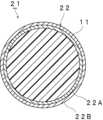
図1は、本発明の第1の実施形態に係る導電性粒子を示す断面図である。Figure 1 is a cross-sectional view showing a conductive particle according to a first embodiment of the present invention.
図1に示す導電性粒子1は、樹脂粒子11と、樹脂粒子11の表面上に配置された導電部2とを有する。導電部2は、樹脂粒子11の表面に接している。導電部2は、樹脂粒子11の表面を覆っている。導電性粒子1は、樹脂粒子11の表面が導電部2により被覆された被覆粒子である。導電性粒子1では、導電部2は、単層の導電部(導電層)である。The
図2は、本発明の第2の実施形態に係る導電性粒子を示す断面図である。Figure 2 is a cross-sectional view showing a conductive particle according to a second embodiment of the present invention.
図2に示す導電性粒子21は、樹脂粒子11と、樹脂粒子11の表面上に配置された導電部22とを有する。導電部22は全体で、樹脂粒子11側に第1の導電部22Aと、樹脂粒子11側とは反対側に第2の導電部22Bとを有する。2 has a
図1に示す導電性粒子1と図2に示す導電性粒子21とでは、導電部22のみが異なっている。すなわち、導電性粒子1では、1層構造の導電部が形成されているのに対し、導電性粒子21では、2層構造の第1の導電部22A及び第2の導電部22Bが形成されている。第1の導電部22Aと第2の導電部22Bとは、異なる導電部として形成されていてもよく、同一の導電部として形成されていてもよい。The only difference between the
第1の導電部22Aは、樹脂粒子11の表面上に配置されている。樹脂粒子11と第2の導電部22Bとの間に、第1の導電部22Aが配置されている。第1の導電部22Aは、樹脂粒子11に接している。第2の導電部22Bは、第1の導電部22Aに接している。樹脂粒子11の表面上に第1の導電部22Aが配置されており、第1の導電部22Aの表面上に第2の導電部22Bが配置されている。The first conductive portion 22A is disposed on the surface of the
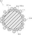
図3は、本発明の第3の実施形態に係る導電性粒子を示す断面図である。Figure 3 is a cross-sectional view showing a conductive particle according to a third embodiment of the present invention.
図3に示す導電性粒子31は、樹脂粒子11と、導電部32と、複数の芯物質33と、複数の絶縁性物質34とを有する。導電部32は、樹脂粒子11の表面上に配置されている。複数の芯物質33は、樹脂粒子11の表面上に配置されている。導電部32は、樹脂粒子11と、複数の芯物質33とを覆うように、樹脂粒子11の表面上に配置されている。導電性粒子31では、導電部32は、単層の導電部(導電層)である。The
導電性粒子31は外表面に、複数の突起31aを有する。導電性粒子31では、導電部32は外表面に、複数の突起32aを有する。複数の芯物質33は、導電部32の外表面を隆起させている。導電部32の外表面が複数の芯物質33によって隆起されていることで、突起31a及び32aが形成されている。複数の芯物質33は導電部32内に埋め込まれている。突起31a及び32aの内側に、芯物質33が配置されている。導電性粒子31では、突起31a及び32aを形成するために、複数の芯物質33を用いている。上記導電性粒子では、上記突起を形成するために、複数の上記芯物質を用いなくてもよい。上記導電性粒子は、複数の上記芯物質を備えていなくてもよい。The
導電性粒子31は、導電部32の外表面上に配置された絶縁性物質34を有する。導電部32の外表面の少なくとも一部の領域が、絶縁性物質34により被覆されている。絶縁性物質34は絶縁性を有する材料により形成されており、絶縁性粒子である。このように、本発明に係る導電性粒子は、導電部の外表面上に配置された絶縁性物質を有していてもよい。但し、上記導電性粒子は、絶縁性物質を必ずしも有していなくてもよい。上記導電性粒子は、複数の絶縁性物質を備えていなくてもよい。The
導電部:
上記導電部を形成するための金属は特に限定されない。該金属としては、例えば、金、銀、パラジウム、銅、白金、亜鉛、鉄、錫、鉛、アルミニウム、コバルト、インジウム、ニッケル、クロム、チタン、アンチモン、ビスマス、タリウム、ゲルマニウム、カドミウム、ケイ素、タングステン、モリブデン及びこれらの合金等が挙げられる。また、上記金属としては、錫ドープ酸化インジウム(ITO)及びはんだ等が挙げられる。電極間の接続抵抗をより一層低くすることができるので、錫を含む合金、ニッケル、パラジウム、銅又は金が好ましく、ニッケル又はパラジウムが好ましい。 Conductive part:
The metal for forming the conductive part is not particularly limited. Examples of the metal include gold, silver, palladium, copper, platinum, zinc, iron, tin, lead, aluminum, cobalt, indium, nickel, chromium, titanium, antimony, bismuth, thallium, germanium, cadmium, silicon, tungsten, molybdenum, and alloys thereof. Examples of the metal include tin-doped indium oxide (ITO) and solder. Since the connection resistance between electrodes can be further reduced, alloys containing tin, nickel, palladium, copper, or gold are preferred, and nickel or palladium is preferred.
また、導通信頼性を効果的に高めることができるので、上記導電部及び上記導電部の外表面部分はニッケルを含むことが好ましい。ニッケルを含む導電部100重量%中のニッケルの含有量は、好ましくは10重量%以上、より好ましくは50重量%以上、より一層好ましくは60重量%以上、さらに好ましくは70重量%以上、特に好ましくは90重量%以上である。上記ニッケルを含む導電部100重量%中のニッケルの含有量は、97重量%以上であってもよく、97.5重量%以上であってもよく、98重量%以上であってもよい。In addition, since the conductive part and the outer surface part of the conductive part contain nickel, it is preferable that the conductive part and the outer surface part of the conductive part contain nickel, since the conductive reliability can be effectively improved. The nickel content in 100% by weight of the conductive part containing nickel is preferably 10% by weight or more, more preferably 50% by weight or more, even more preferably 60% by weight or more, even more preferably 70% by weight or more, and particularly preferably 90% by weight or more. The nickel content in 100% by weight of the conductive part containing nickel may be 97% by weight or more, 97.5% by weight or more, or 98% by weight or more.
なお、導電部の表面には、酸化により水酸基が存在することが多い。一般的に、ニッケルにより形成された導電部の表面には、酸化により水酸基が存在する。このような水酸基を有する導電部の表面(導電性粒子の表面)に、化学結合を介して、絶縁性物質を配置することができる。In addition, hydroxyl groups are often present on the surface of the conductive part due to oxidation. Generally, hydroxyl groups are present on the surface of a conductive part formed from nickel due to oxidation. An insulating substance can be placed on the surface of a conductive part (surface of a conductive particle) that has such hydroxyl groups via chemical bonding.
導電性粒子1,31のように、上記導電部は、1つの層により形成されていてもよい。導電性粒子21のように、導電部は、複数の層により形成されていてもよい。すなわち、導電部は、2層以上の積層構造を有していてもよい。導電部が複数の層により形成されている場合には、最外層は、金層、ニッケル層、パラジウム層、銅層又は錫と銀とを含む合金層であることが好ましく、金層であることがより好ましい。最外層がこれらの好ましい導電部である場合には、電極間の接続抵抗をより一層効果的に低くすることができる。また、最外層が金層である場合には、耐腐食性をより一層効果的に高めることができる。As in the
上記樹脂粒子の表面に上記導電部を形成する方法は特に限定されない。上記導電部を形成する方法としては、例えば、無電解めっきによる方法、電気めっきによる方法、物理的蒸着による方法、並びに金属粉末もしくは金属粉末とバインダーとを含むペーストを樹脂粒子の表面にコーティングする方法等が挙げられる。導電部の形成が簡便であるので、無電解めっきによる方法が好ましい。上記物理的蒸着による方法としては、真空蒸着、イオンプレーティング及びイオンスパッタリング等の方法が挙げられる。The method for forming the conductive portion on the surface of the resin particles is not particularly limited. Examples of the method for forming the conductive portion include an electroless plating method, an electroplating method, a physical vapor deposition method, and a method for coating the surface of the resin particles with a metal powder or a paste containing a metal powder and a binder. The electroless plating method is preferred because the conductive portion is easily formed. Examples of the physical vapor deposition method include vacuum deposition, ion plating, and ion sputtering.
上記導電性粒子の粒子径は、好ましくは0.5μm以上、より好ましくは1.0μm以上であり、好ましくは500μm以下、より好ましくは450μm以下、より一層好ましくは100μm以下、さらに好ましくは50μm以下、特に好ましくは20μm以下である。上記導電性粒子の粒子径が、上記下限以上及び上記上限以下であると、導電性粒子を用いて電極間を接続した場合に、導電性粒子と電極との接触面積が十分に大きくなり、かつ導電部を形成する際に凝集した導電性粒子が形成され難くなる。また、導電性粒子を介して接続された電極間の間隔が大きくなりすぎず、かつ導電部が樹脂粒子の表面から剥離し難くなる。また、上記導電性粒子の粒子径が、上記下限以上及び上記上限以下であると、導電性粒子を導電材料の用途に好適に使用可能である。The particle diameter of the conductive particles is preferably 0.5 μm or more, more preferably 1.0 μm or more, and preferably 500 μm or less, more preferably 450 μm or less, even more preferably 100 μm or less, even more preferably 50 μm or less, and particularly preferably 20 μm or less. If the particle diameter of the conductive particles is equal to or greater than the lower limit and equal to or less than the upper limit, when electrodes are connected using the conductive particles, the contact area between the conductive particles and the electrodes becomes sufficiently large, and it becomes difficult for aggregated conductive particles to be formed when forming the conductive part. In addition, the gap between the electrodes connected via the conductive particles does not become too large, and the conductive part becomes difficult to peel off from the surface of the resin particle. In addition, if the particle diameter of the conductive particles is equal to or greater than the lower limit and equal to or less than the upper limit, the conductive particles can be suitably used for conductive material applications.
上記導電性粒子の粒子径は、導電性粒子が真球状である場合には、直径を示し、導電性粒子が真球状ではない場合には、最大径を示す。The particle diameter of the above conductive particles indicates the diameter if the conductive particles are spherical, and indicates the maximum diameter if the conductive particles are not spherical.
上記導電性粒子の粒子径は、平均粒子径であることが好ましく、数平均粒子径であることがより好ましい。上記導電性粒子の粒子径は、例えば、任意の導電性粒子50個を電子顕微鏡又は光学顕微鏡にて観察し、平均値を算出することや、複数回のレーザー回折式粒度分布測定装置による測定結果の平均値を算出することにより求められる。The particle diameter of the conductive particles is preferably an average particle diameter, and more preferably a number average particle diameter. The particle diameter of the conductive particles can be determined, for example, by observing 50 arbitrary conductive particles with an electron microscope or optical microscope and calculating the average value, or by calculating the average value of the measurement results obtained multiple times using a laser diffraction particle size distribution analyzer.
上記導電部の厚みは、好ましくは0.005μm以上、より好ましくは0.01μm以上であり、好ましくは10μm以下、より好ましくは1μm以下、さらに好ましくは0.3μm以下である。上記導電部の厚みが、上記下限以上及び上記上限以下であると、十分な導電性が得られ、かつ導電性粒子が硬くなりすぎずに、電極間の接続の際に導電性粒子が十分に変形する。The thickness of the conductive portion is preferably 0.005 μm or more, more preferably 0.01 μm or more, and preferably 10 μm or less, more preferably 1 μm or less, and even more preferably 0.3 μm or less. When the thickness of the conductive portion is equal to or greater than the lower limit and equal to or less than the upper limit, sufficient conductivity is obtained, and the conductive particles do not become too hard, and the conductive particles deform sufficiently when connecting the electrodes.
上記導電部が複数の層により形成されている場合に、最外層の導電部の厚みは、好ましくは0.001μm以上、より好ましくは0.01μm以上であり、好ましくは0.5μm以下、より好ましくは0.1μm以下である。上記最外層の導電部の厚みが、上記下限以上及び上記上限以下であると、最外層の導電部による被覆が均一になり、耐腐食性が十分に高くなり、かつ電極間の接続抵抗が十分に低くなる。また、上記最外層が金層である場合に、金層の厚みが薄いほど、コストが低くなる。When the conductive portion is formed of multiple layers, the thickness of the conductive portion of the outermost layer is preferably 0.001 μm or more, more preferably 0.01 μm or more, and preferably 0.5 μm or less, more preferably 0.1 μm or less. When the thickness of the conductive portion of the outermost layer is equal to or greater than the lower limit and equal to or less than the upper limit, the coating by the conductive portion of the outermost layer becomes uniform, the corrosion resistance becomes sufficiently high, and the connection resistance between the electrodes becomes sufficiently low. In addition, when the outermost layer is a gold layer, the thinner the gold layer, the lower the cost.
上記導電部の厚みは、例えば透過型電子顕微鏡(TEM)を用いて、導電性粒子の断面を観察することにより測定できる。上記導電部の厚みについては、任意の導電部の厚み5箇所の平均値を1個の導電性粒子の導電部の厚みとして算出することが好ましく、導電部全体の厚みの平均値を1個の導電部の厚みとして算出することがより好ましい。複数の導電性粒子の場合には、上記導電部の厚みは、好ましくは、任意の導電性粒子10個について、これらの平均値を算出して求められる。The thickness of the conductive part can be measured by observing the cross section of the conductive particle, for example, using a transmission electron microscope (TEM). It is preferable to calculate the thickness of the conductive part as the average value of the thicknesses of five arbitrary conductive parts as the thickness of the conductive part of one conductive particle, and it is more preferable to calculate the average value of the thickness of the entire conductive part as the thickness of one conductive part. In the case of multiple conductive particles, the thickness of the conductive part is preferably determined by calculating the average value of these for arbitrary 10 conductive particles.
芯物質:
上記導電性粒子は、上記導電部の外表面に複数の突起を有することが好ましい。上記導電性粒子が、上記導電部の外表面に複数の突起を有していることで、電極間の導通信頼性をより一層高めることができる。上記導電性粒子により接続される電極の表面には、酸化被膜が形成されていることが多い。さらに、上記導電性粒子の導電部の表面には、酸化被膜が形成されていることが多い。上記突起を有する導電性粒子を用いることで、電極間に導電性粒子を配置した後、圧着させることにより、突起により酸化被膜が効果的に排除される。このため、電極と導電性粒子とをより一層確実に接触させることができ、電極間の接続抵抗をより一層効果的に低くすることができる。さらに、上記導電性粒子が表面に絶縁性物質を有する場合、又は導電性粒子がバインダー樹脂中に分散されて導電材料として用いられる場合に、導電性粒子の突起によって、導電性粒子と電極との間の絶縁性物質やバインダー樹脂が効果的に排除される。このため、電極間の導通信頼性をより一層効果的に高めることができる。 Core material:
The conductive particles preferably have a plurality of protrusions on the outer surface of the conductive part. The conductive particles have a plurality of protrusions on the outer surface of the conductive part, which can further increase the reliability of conduction between the electrodes. An oxide film is often formed on the surface of the electrodes connected by the conductive particles. Furthermore, an oxide film is often formed on the surface of the conductive part of the conductive particles. By using the conductive particles having the protrusions, the conductive particles are placed between the electrodes and then pressed together, so that the oxide film is effectively removed by the protrusions. Therefore, the electrodes and the conductive particles can be more reliably contacted, and the connection resistance between the electrodes can be more effectively reduced. Furthermore, when the conductive particles have an insulating material on their surfaces, or when the conductive particles are dispersed in a binder resin and used as a conductive material, the insulating material or binder resin between the conductive particles and the electrodes is effectively removed by the protrusions of the conductive particles. Therefore, the reliability of conduction between the electrodes can be more effectively increased.
上記芯物質が上記導電部中に埋め込まれていることによって、上記導電部の外表面に複数の突起を容易に形成することができる。但し、導電性粒子の導電部の表面に突起を形成するために、芯物質を必ずしも用いなくてもよい。By embedding the core material in the conductive portion, multiple protrusions can be easily formed on the outer surface of the conductive portion. However, it is not necessary to use a core material to form protrusions on the surface of the conductive portion of the conductive particle.
上記突起を形成する方法としては、樹脂粒子の表面に芯物質を付着させた後、無電解めっきにより導電部を形成する方法、並びに樹脂粒子の表面に無電解めっきにより導電部を形成した後、芯物質を付着させ、さらに無電解めっきにより導電部を形成する方法等が挙げられる。上記突起を形成する他の方法としては、樹脂粒子の表面上に、第1の導電部を形成した後、該第1の導電部上に芯物質を配置し、次に第2の導電部を形成する方法、並びに樹脂粒子の表面上に導電部(第1の導電部又は第2の導電部等)を形成する途中段階で、芯物質を添加する方法等が挙げられる。また、突起を形成するために、上記芯物質を用いずに、樹脂粒子に無電解めっきにより導電部を形成した後、導電部の表面上に突起状にめっきを析出させ、さらに無電解めっきにより導電部を形成する方法等を用いてもよい。Examples of the method for forming the protrusions include a method of attaching a core material to the surface of a resin particle and then forming a conductive part by electroless plating, and a method of forming a conductive part on the surface of a resin particle by electroless plating, attaching a core material, and further forming a conductive part by electroless plating. Other methods for forming the protrusions include a method of forming a first conductive part on the surface of a resin particle, placing a core material on the first conductive part, and then forming a second conductive part, as well as a method of adding a core material during the process of forming a conductive part (such as a first conductive part or a second conductive part) on the surface of a resin particle. In addition, in order to form the protrusions, a method may be used in which, without using the core material, a conductive part is formed on a resin particle by electroless plating, plating is precipitated in the form of protrusions on the surface of the conductive part, and then a conductive part is formed by electroless plating.
上記樹脂粒子の表面上に芯物質を配置する方法としては、例えば、樹脂粒子の分散液中に、芯物質を添加し、樹脂粒子の表面に芯物質を、ファンデルワールス力により集積させ、付着させる方法、並びに樹脂粒子を入れた容器に、芯物質を添加し、容器の回転等による機械的な作用により樹脂粒子の表面に芯物質を付着させる方法等が挙げられる。付着させる芯物質の量を制御しやすいため、分散液中の樹脂粒子の表面に芯物質を集積させ、付着させる方法が好ましい。Examples of methods for disposing a core substance on the surface of the resin particles include a method in which a core substance is added to a dispersion of resin particles, and the core substance is accumulated and attached to the surface of the resin particles by van der Waals forces, and a method in which a core substance is added to a container containing resin particles, and the core substance is attached to the surface of the resin particles by mechanical action such as rotating the container. The method in which the core substance is accumulated and attached to the surface of the resin particles in the dispersion is preferred because it is easy to control the amount of core substance to be attached.
上記芯物質の材料は特に限定されない。上記芯物質の材料としては、例えば、導電性物質及び非導電性物質が挙げられる。上記導電性物質としては、金属、金属の酸化物、黒鉛等の導電性非金属及び導電性ポリマー等が挙げられる。上記導電性ポリマーとしては、ポリアセチレン等が挙げられる。上記非導電性物質としては、シリカ、アルミナ、チタン酸バリウム及びジルコニア等が挙げられる。導電性を高めることができ、さらに接続抵抗を効果的に低くすることができるので、金属が好ましい。上記芯物質は金属粒子であることが好ましい。上記芯物質の材料である金属としては、上記導電部を形成するための金属として挙げた金属を適宜使用可能である。The material of the core substance is not particularly limited. Examples of the material of the core substance include conductive substances and non-conductive substances. Examples of the conductive substances include conductive non-metals such as metals, metal oxides, and graphite, and conductive polymers. Examples of the conductive polymers include polyacetylene. Examples of the non-conductive substances include silica, alumina, barium titanate, and zirconia. Metals are preferred because they can increase the conductivity and effectively reduce the connection resistance. The core substance is preferably a metal particle. As the metal that is the material of the core substance, the metals listed as the metals for forming the conductive portion can be appropriately used.
絶縁性物質:
上記導電性粒子は、上記導電部の表面上に配置された絶縁性物質を備えることが好ましい。この場合には、導電性粒子を電極間の接続に用いると、隣接する電極間の短絡をより一層防止できる。具体的には、複数の導電性粒子が接触したときに、複数の電極間に絶縁性物質が存在するので、上下の電極間ではなく横方向に隣り合う電極間の短絡を防止できる。なお、電極間の接続の際に、2つの電極で導電性粒子を加圧することにより、導電性粒子の導電部と電極との間の絶縁性物質を容易に排除できる。上記導電性粒子が導電部の外表面に複数の突起を有する場合には、導電性粒子の導電部と電極との間の絶縁性物質をより一層容易に排除できる。 Insulating materials:
The conductive particles preferably have an insulating material disposed on the surface of the conductive portion. In this case, when the conductive particles are used for connecting the electrodes, short-circuiting between adjacent electrodes can be further prevented. Specifically, when a plurality of conductive particles contact each other, an insulating material exists between the plurality of electrodes, so that short-circuiting between adjacent electrodes in the horizontal direction, rather than between upper and lower electrodes, can be prevented. In addition, when connecting the electrodes, the insulating material between the conductive portion of the conductive particles and the electrode can be easily removed by pressing the conductive particles with two electrodes. When the conductive particles have a plurality of protrusions on the outer surface of the conductive portion, the insulating material between the conductive portion of the conductive particles and the electrode can be more easily removed.
電極間の圧着時に上記絶縁性物質をより一層容易に排除できることから、上記絶縁性物質は、絶縁性粒子であることが好ましい。It is preferable that the insulating material is insulating particles, since this makes it easier to remove the insulating material when the electrodes are pressed together.
上記絶縁性物質の材料としては、ポリオレフィン化合物、(メタ)アクリレート重合体、(メタ)アクリレート共重合体、ブロックポリマー、熱可塑性樹脂、熱可塑性樹脂の架橋物、熱硬化性樹脂及び水溶性樹脂等が挙げられる。上記絶縁性物質の材料は、1種のみが用いられてもよく、2種以上が併用されてもよい。Examples of the insulating material include polyolefin compounds, (meth)acrylate polymers, (meth)acrylate copolymers, block polymers, thermoplastic resins, crosslinked thermoplastic resins, thermosetting resins, and water-soluble resins. Only one type of insulating material may be used, or two or more types may be used in combination.
上記ポリオレフィン化合物としては、ポリエチレン、エチレン-酢酸ビニル共重合体及びエチレン-アクリル酸エステル共重合体等が挙げられる。上記(メタ)アクリレート重合体としては、ポリメチル(メタ)アクリレート、ポリドデシル(メタ)アクリレート及びポリステアリル(メタ)アクリレート等が挙げられる。上記ブロックポリマーとしては、ポリスチレン、スチレン-アクリル酸エステル共重合体、SB型スチレン-ブタジエンブロック共重合体、及びSBS型スチレン-ブタジエンブロック共重合体、並びにこれらの水素添加物等が挙げられる。上記熱可塑性樹脂としては、ビニル重合体及びビニル共重合体等が挙げられる。上記熱硬化性樹脂としては、エポキシ樹脂、フェノール樹脂及びメラミン樹脂等が挙げられる。上記熱可塑性樹脂の架橋としては、ポリエチレングリコールメタクリレート、アルコキシ化トリメチロールプロパンメタクリレートやアルコキシ化ペンタエリスリトールメタクリレート等の導入が挙げられる。上記水溶性樹脂としては、ポリビニルアルコール、ポリアクリル酸、ポリアクリルアミド、ポリビニルピロリドン、ポリエチレンオキシド及びメチルセルロース等が挙げられる。また、重合度の調整に、連鎖移動剤を使用してもよい。連鎖移動剤としては、チオールや四塩化炭素等が挙げられる。Examples of the polyolefin compound include polyethylene, ethylene-vinyl acetate copolymer, and ethylene-acrylic acid ester copolymer. Examples of the (meth)acrylate polymer include polymethyl (meth)acrylate, polydodecyl (meth)acrylate, and polystearyl (meth)acrylate. Examples of the block polymer include polystyrene, styrene-acrylic acid ester copolymer, SB type styrene-butadiene block copolymer, SBS type styrene-butadiene block copolymer, and hydrogenated products thereof. Examples of the thermoplastic resin include vinyl polymer and vinyl copolymer. Examples of the thermosetting resin include epoxy resin, phenolic resin, and melamine resin. Examples of the crosslinking of the thermoplastic resin include the introduction of polyethylene glycol methacrylate, alkoxylated trimethylolpropane methacrylate, and alkoxylated pentaerythritol methacrylate. Examples of the water-soluble resin include polyvinyl alcohol, polyacrylic acid, polyacrylamide, polyvinylpyrrolidone, polyethylene oxide, and methylcellulose. In addition, a chain transfer agent may be used to adjust the degree of polymerization. Examples of the chain transfer agent include thiol and carbon tetrachloride.
上記導電部の表面上に絶縁性物質を配置する方法としては、化学的方法、及び物理的もしくは機械的方法等が挙げられる。上記化学的方法としては、例えば、界面重合法、粒子存在下での懸濁重合法及び乳化重合法等が挙げられる。上記物理的もしくは機械的方法としては、スプレードライ、ハイブリダイゼーション、静電付着法、噴霧法、ディッピング及び真空蒸着による方法等が挙げられる。絶縁性物質が脱離し難いことから、上記導電部の表面に、化学結合を介して上記絶縁性物質を配置する方法が好ましい。Methods for disposing an insulating material on the surface of the conductive part include chemical methods and physical or mechanical methods. Examples of the chemical methods include interfacial polymerization, suspension polymerization in the presence of particles, and emulsion polymerization. Examples of the physical or mechanical methods include spray drying, hybridization, electrostatic adhesion, spraying, dipping, and vacuum deposition. Since the insulating material is difficult to remove, a method in which the insulating material is disposed on the surface of the conductive part via a chemical bond is preferred.
上記導電部の外表面、及び絶縁性物質の表面はそれぞれ、反応性官能基を有する化合物によって被覆されていてもよい。導電部の外表面と絶縁性物質の表面とは、直接化学結合していなくてもよく、反応性官能基を有する化合物によって間接的に化学結合していてもよい。導電部の外表面にカルボキシル基を導入した後、該カルボキシル基がポリエチレンイミン等の高分子電解質を介して絶縁性物質の表面の官能基と化学結合していても構わない。The outer surface of the conductive part and the surface of the insulating material may each be coated with a compound having a reactive functional group. The outer surface of the conductive part and the surface of the insulating material may not be directly chemically bonded, but may be indirectly chemically bonded via a compound having a reactive functional group. After a carboxyl group is introduced onto the outer surface of the conductive part, the carboxyl group may be chemically bonded to a functional group on the surface of the insulating material via a polymer electrolyte such as polyethyleneimine.
(導電材料)
本発明に係る導電材料は、上述した導電性粒子と、バインダーとを含む。上記導電性粒子は、バインダー中に分散されて用いられることが好ましく、バインダー中に分散されて導電材料として用いられることが好ましい。上記導電材料は、異方性導電材料であることが好ましい。上記導電材料は、電極間の電気的な接続に用いられることが好ましい。上記導電材料は回路接続用導電材料であることが好ましい。 (Conductive materials)
The conductive material according to the present invention includes the conductive particles described above and a binder. The conductive particles are preferably dispersed in the binder and used, and are preferably dispersed in the binder and used as a conductive material. The conductive material is preferably an anisotropic conductive material. The conductive material is preferably used for electrical connection between electrodes. The conductive material is preferably a conductive material for circuit connection.
上記バインダーは特に限定されない。上記バインダーとして、公知の絶縁性の樹脂が用いられる。上記バインダーは、熱可塑性成分(熱可塑性化合物)又は硬化性成分を含むことが好ましく、硬化性成分を含むことがより好ましい。上記硬化性成分としては、光硬化性成分及び熱硬化性成分が挙げられる。上記光硬化性成分は、光硬化性化合物及び光重合開始剤を含むことが好ましい。上記熱硬化性成分は、熱硬化性化合物及び熱硬化剤を含むことが好ましい。The binder is not particularly limited. A known insulating resin is used as the binder. The binder preferably contains a thermoplastic component (thermoplastic compound) or a curable component, and more preferably contains a curable component. Examples of the curable component include a photocurable component and a thermosetting component. The photocurable component preferably contains a photocurable compound and a photopolymerization initiator. The thermosetting component preferably contains a thermosetting compound and a thermosetting agent.
上記バインダーとしては、ビニル樹脂、熱可塑性樹脂、硬化性樹脂、熱可塑性ブロック共重合体及びエラストマー等が挙げられる。上記バインダーは1種のみが用いられてもよく、2種以上が併用されてもよい。Examples of the binder include vinyl resins, thermoplastic resins, curable resins, thermoplastic block copolymers, and elastomers. Only one type of the binder may be used, or two or more types may be used in combination.
上記ビニル樹脂としては、例えば、酢酸ビニル樹脂、アクリル樹脂及びスチレン樹脂等が挙げられる。上記熱可塑性樹脂としては、例えば、ポリオレフィン樹脂、エチレン-酢酸ビニル共重合体及びポリアミド樹脂等が挙げられる。上記硬化性樹脂としては、例えば、エポキシ樹脂、ウレタン樹脂、ポリイミド樹脂及び不飽和ポリエステル樹脂等が挙げられる。なお、上記硬化性樹脂は、常温硬化型樹脂、熱硬化型樹脂、光硬化型樹脂又は湿気硬化型樹脂であってもよい。上記硬化性樹脂は、硬化剤と併用されてもよい。上記熱可塑性ブロック共重合体としては、例えば、スチレン-ブタジエン-スチレンブロック共重合体、スチレン-イソプレン-スチレンブロック共重合体、スチレン-ブタジエン-スチレンブロック共重合体の水素添加物、及びスチレン-イソプレン-スチレンブロック共重合体の水素添加物等が挙げられる。上記エラストマーとしては、例えば、スチレン-ブタジエン共重合ゴム、及びアクリロニトリル-スチレンブロック共重合ゴム等が挙げられる。Examples of the vinyl resin include vinyl acetate resin, acrylic resin, and styrene resin. Examples of the thermoplastic resin include polyolefin resin, ethylene-vinyl acetate copolymer, and polyamide resin. Examples of the curable resin include epoxy resin, urethane resin, polyimide resin, and unsaturated polyester resin. The curable resin may be a room temperature curable resin, a thermosetting resin, a photocurable resin, or a moisture curable resin. The curable resin may be used in combination with a curing agent. Examples of the thermoplastic block copolymer include styrene-butadiene-styrene block copolymer, styrene-isoprene-styrene block copolymer, hydrogenated styrene-butadiene-styrene block copolymer, and hydrogenated styrene-isoprene-styrene block copolymer. Examples of the elastomer include styrene-butadiene copolymer rubber and acrylonitrile-styrene block copolymer rubber.
上記導電材料は、上記導電性粒子及び上記バインダーの他に、例えば、充填剤、増量剤、軟化剤、可塑剤、重合触媒、硬化触媒、着色剤、酸化防止剤、熱安定剤、光安定剤、紫外線吸収剤、滑剤、帯電防止剤及び難燃剤等の各種添加剤を含んでいてもよい。In addition to the conductive particles and the binder, the conductive material may contain various additives such as fillers, extenders, softeners, plasticizers, polymerization catalysts, curing catalysts, colorants, antioxidants, heat stabilizers, light stabilizers, UV absorbers, lubricants, antistatic agents, and flame retardants.
上記バインダー中に上記導電性粒子を分散させる方法は、従来公知の分散方法を用いることができ、特に限定されない。上記バインダー中に上記導電性粒子を分散させる方法としては、上記バインダー中に上記導電性粒子を添加した後、プラネタリーミキサー等で混練して分散させる方法、上記導電性粒子を水又は有機溶剤中にホモジナイザー等を用いて均一に分散させた後、上記バインダー中に添加し、プラネタリーミキサー等で混練して分散させる方法が挙げられる。さらに、上記バインダー中に上記導電性粒子を分散させる方法としては、上記バインダーを水又は有機溶剤等で希釈した後、上記導電性粒子を添加し、プラネタリーミキサー等で混練して分散させる方法等が挙げられる。The method of dispersing the conductive particles in the binder can be a conventionally known dispersion method, and is not particularly limited. Examples of the method of dispersing the conductive particles in the binder include a method of adding the conductive particles to the binder and then kneading and dispersing them with a planetary mixer or the like, and a method of uniformly dispersing the conductive particles in water or an organic solvent using a homogenizer or the like, adding them to the binder, and kneading and dispersing them with a planetary mixer or the like. Furthermore, examples of the method of dispersing the conductive particles in the binder include a method of diluting the binder with water or an organic solvent, adding the conductive particles, and kneading and dispersing them with a planetary mixer or the like.
上記導電材料は、導電ペースト及び導電フィルム等として使用され得る。上記導電材料が、導電フィルムである場合には、導電性粒子を含む導電フィルムに、導電性粒子を含まないフィルムが積層されていてもよい。上記導電ペーストは、異方性導電ペーストであることが好ましい。上記導電フィルムは、異方性導電フィルムであることが好ましい。The conductive material can be used as a conductive paste, a conductive film, etc. When the conductive material is a conductive film, a film not containing conductive particles may be laminated on a conductive film containing conductive particles. The conductive paste is preferably an anisotropic conductive paste. The conductive film is preferably an anisotropic conductive film.
上記導電材料100重量%中、上記バインダーの含有量は、好ましくは10重量%以上、より好ましくは30重量%以上、さらに好ましくは50重量%以上、特に好ましくは70重量%以上であり、好ましくは99.99重量%以下、より好ましくは99.9重量%以下である。上記バインダーの含有量が、上記下限以上及び上記上限以下であると、電極間に導電性粒子が効率的に配置され、導電材料により接続された接続対象部材の接続信頼性がより一層高くなる。In 100% by weight of the conductive material, the content of the binder is preferably 10% by weight or more, more preferably 30% by weight or more, even more preferably 50% by weight or more, particularly preferably 70% by weight or more, and is preferably 99.99% by weight or less, more preferably 99.9% by weight or less. When the content of the binder is equal to or more than the lower limit and equal to or less than the upper limit, the conductive particles are efficiently arranged between the electrodes, and the connection reliability of the connection target members connected by the conductive material is further increased.
上記導電材料100重量%中、上記導電性粒子の含有量は、好ましくは0.01重量%以上、より好ましくは0.1重量%以上であり、好ましくは80重量%以下、より好ましくは60重量%以下、さらに好ましくは40重量%以下、特に好ましくは20重量%以下、最も好ましくは10重量%以下である。上記導電性粒子の含有量が、上記下限以上及び上記上限以下であると、電極間の導通信頼性がより一層高くなる。In 100% by weight of the conductive material, the content of the conductive particles is preferably 0.01% by weight or more, more preferably 0.1% by weight or more, and is preferably 80% by weight or less, more preferably 60% by weight or less, even more preferably 40% by weight or less, particularly preferably 20% by weight or less, and most preferably 10% by weight or less. When the content of the conductive particles is equal to or more than the lower limit and equal to or less than the upper limit, the reliability of conduction between the electrodes is further increased.
(接着剤)
本発明に係る接着剤は、上述した樹脂粒子と、バインダーとを含む。上記樹脂粒子は、バインダー中に分散されて用いられることが好ましく、バインダー中に分散されて接着剤として用いられることが好ましい。上記樹脂粒子は、バインダー中でスペーサとして用いられることが好ましい。上記接着剤は、導電性粒子を含んでいなくてもよい。 (glue)
The adhesive according to the present invention includes the above-mentioned resin particles and a binder. The resin particles are preferably dispersed in the binder and used as an adhesive, and the resin particles are preferably used as a spacer in the binder. The adhesive does not need to include conductive particles.
上記接着剤は、2つの接続対象部材を接着する接着層を形成するために用いられる。さらに、上記接着剤は、上記接着層のギャップを高精度に制御するため、又は上記接着層の応力を緩和するため等に用いられる。The adhesive is used to form an adhesive layer that bonds two components to be connected. Furthermore, the adhesive is used to control the gap of the adhesive layer with high precision, or to relieve stress in the adhesive layer, etc.
上記バインダーは特に限定されない。上記バインダーの具体例としては、上述した導電材料に用いられるバインダー等が挙げられる。上記接着剤は、上記バインダーとして、エポキシ樹脂を含むことが好ましい。The binder is not particularly limited. Specific examples of the binder include the binders used in the conductive materials described above. It is preferable that the adhesive contains an epoxy resin as the binder.
上記接着剤100重量%中、上記バインダーの含有量は、好ましくは10重量%以上、より好ましくは30重量%以上、さらに好ましくは50重量%以上、特に好ましくは70重量%以上であり、好ましくは99.99重量%以下、より好ましくは99.9重量%以下である。上記バインダーの含有量が、上記下限以上及び上記上限以下であると、上記接着層の接着力をより一層効果的に高めることができ、上記樹脂粒子がスペーサとしての機能をより一層効果的に発揮することができる。In 100% by weight of the adhesive, the content of the binder is preferably 10% by weight or more, more preferably 30% by weight or more, even more preferably 50% by weight or more, particularly preferably 70% by weight or more, and is preferably 99.99% by weight or less, more preferably 99.9% by weight or less. When the content of the binder is equal to or more than the lower limit and equal to or less than the upper limit, the adhesive strength of the adhesive layer can be increased more effectively, and the resin particles can more effectively function as spacers.
上記接着剤100重量%中、上記樹脂粒子の含有量は、好ましくは0.01重量%以上、より好ましくは0.1重量%以上であり、好ましくは80重量%以下、より好ましくは60重量%以下、さらに好ましくは40重量%以下、特に好ましくは20重量%以下、最も好ましくは10重量%以下である。上記樹脂粒子の含有量が、上記下限以上及び上記上限以下であると、上記樹脂粒子がスペーサとしての機能をより一層効果的に発揮することができる。In 100% by weight of the adhesive, the content of the resin particles is preferably 0.01% by weight or more, more preferably 0.1% by weight or more, and is preferably 80% by weight or less, more preferably 60% by weight or less, even more preferably 40% by weight or less, particularly preferably 20% by weight or less, and most preferably 10% by weight or less. When the content of the resin particles is equal to or more than the lower limit and equal to or less than the upper limit, the resin particles can more effectively function as spacers.
(接続構造体)
上記導電性粒子を用いて、又は上記導電性粒子とバインダーとを含む導電材料を用いて、接続対象部材を接続することにより、接続構造体を得ることができる。 (Connection structure)
A connection structure can be obtained by connecting members to be connected using the conductive particles or a conductive material containing the conductive particles and a binder.
本発明に係る接続構造体は、第1の電極を表面に有する第1の接続対象部材と、第2の電極を表面に有する第2の接続対象部材と、上記第1の接続対象部材と、上記第2の接続対象部材とを接続している接続部とを備える。上記接続部の材料が、上述した樹脂粒子を含む。上記接続部の材料が、上述した導電性粒子であるか、又は上述した導電材料であることが好ましい。上記接続部が、上述した導電性粒子により形成されているか、又は上述した導電材料により形成されている接続構造体であることが好ましい。The connection structure according to the present invention comprises a first connection target member having a first electrode on its surface, a second connection target member having a second electrode on its surface, and a connection part connecting the first connection target member and the second connection target member. The material of the connection part contains the resin particles described above. It is preferable that the material of the connection part is the conductive particles described above or the conductive material described above. It is preferable that the connection part is a connection structure formed from the conductive particles described above or the conductive material described above.
上記導電性粒子が単独で用いられた場合には、接続部自体が導電性粒子である。すなわち、第1,第2の接続対象部材が上記導電性粒子により接続される。上記接続構造体を得るために用いられる上記導電材料は、異方性導電材料であることが好ましい。上記第1の電極と上記第2の電極とが、上記接続部により電気的に接続されていることが好ましい。When the conductive particles are used alone, the connection portion itself is a conductive particle. That is, the first and second connection target members are connected by the conductive particles. The conductive material used to obtain the connection structure is preferably an anisotropic conductive material. It is preferable that the first electrode and the second electrode are electrically connected by the connection portion.
図4は、図1に示す導電性粒子1を用いた接続構造体の一例を示す断面図である。Figure 4 is a cross-sectional view showing an example of a connection structure using the
図4に示す接続構造体41は、第1の接続対象部材42と、第2の接続対象部材43と、第1の接続対象部材42と第2の接続対象部材43とを接続している接続部44とを備える。接続部44は、導電性粒子1とバインダーとを含む導電材料により形成されている。図4では、図示の便宜上、導電性粒子1は略図的に示されている。導電性粒子1に代えて、導電性粒子21,31等の他の導電性粒子を用いてもよい。The
第1の接続対象部材42は表面(上面)に、複数の第1の電極42aを有する。第2の接続対象部材43は表面(下面)に、複数の第2の電極43aを有する。第1の電極42aと第2の電極43aとが、1つ又は複数の導電性粒子1により電気的に接続されている。従って、第1,第2の接続対象部材42,43が導電性粒子1により電気的に接続されている。The first
図5は、本発明に係る樹脂粒子を用いた接続構造体の一例を示す断面図である。Figure 5 is a cross-sectional view showing an example of a connection structure using resin particles according to the present invention.
図5に示す接続構造体51は、第1の接続対象部材52と、第2の接続対象部材53と、第1の接続対象部材52と第2の接続対象部材53とを接着している接着層54とを備える。The
接着層54は、上述した樹脂粒子11を含む。樹脂粒子11は、第1,第2の接続対象部材52,53の双方に接していない。樹脂粒子11は、応力緩和用スペーサとして用いられている。The
接着層54は、ギャップ制御粒子61と、熱硬化性成分62とを含む。接着層54では、ギャップ制御粒子61が、第1,第2の接続対象部材52,53の双方に接している。ギャップ制御粒子61は導電性粒子であってもよく、導電性を有さない粒子であってもよい。上記ギャップ制御粒子は、上述した樹脂粒子であってもよい。熱硬化性成分62は、熱硬化性化合物と熱硬化剤とを含む。熱硬化性成分62は、熱硬化性化合物の硬化物である。熱硬化性成分62は、熱硬化性化合物を硬化させることにより形成されている。The
上記第1の接続対象部材は、第1の電極を表面に有していてもよい。上記第2の接続対象部材は、第2の電極を表面に有していてもよい。The first connection target member may have a first electrode on its surface. The second connection target member may have a second electrode on its surface.
上記接続構造体の製造方法は特に限定されない。接続構造体の製造方法の一例として、第1の接続対象部材と第2の接続対象部材との間に上記導電材料を配置し、積層体を得た後、該積層体を加熱及び加圧する方法等が挙げられる。上記加圧時の圧力は9.8×10⁴Pa~4.9×10⁶Pa程度である。上記加熱時の温度は、120℃~220℃程度である。フレキシブルプリント基板の電極、樹脂フィルム上に配置された電極及びタッチパネルの電極を接続するための上記加圧時の圧力は9.8×10⁴Pa~1.0×10⁶Pa程度である。 The method for producing the connection structure is not particularly limited. One example of the method for producing the connection structure is to place the conductive material between a first connection target member and a second connection target member, obtain a laminate, and then heat and press the laminate. The pressure during the pressurization is about 9.8×10⁴ Pa to 4.9×10⁶ Pa. The temperature during the heating is about 120° C. to 220° C. The pressure during the pressurization for connecting the electrodes of the flexible printed circuit board, the electrodes arranged on the resin film, and the electrodes of the touch panel is about 9.8×10⁴ Pa to 1.0×10⁶ Pa.
上記接続対象部材としては、具体的には、半導体チップ、コンデンサ及びダイオード等の電子部品、並びにプリント基板、フレキシブルプリント基板、ガラスエポキシ基板及びガラス基板等の回路基板等の電子部品等が挙げられる。上記接続対象部材は電子部品であることが好ましい。上記第1の接続対象部材及び上記第2の接続対象部材の内の少なくとも一方は、半導体ウェハ又は半導体チップであることが好ましい。上記接続構造体は、半導体装置であることが好ましい。Specific examples of the connection target members include electronic components such as semiconductor chips, capacitors, and diodes, as well as circuit boards such as printed circuit boards, flexible printed circuit boards, glass epoxy boards, and glass boards. The connection target members are preferably electronic components. At least one of the first connection target member and the second connection target member is preferably a semiconductor wafer or a semiconductor chip. The connection structure is preferably a semiconductor device.
上記導電材料は、電子部品を接続するための導電材料であることが好ましい。上記導電ペーストはペースト状の導電材料であり、ペースト状の状態で接続対象部材上に塗工されることが好ましい。The conductive material is preferably a conductive material for connecting electronic components. The conductive paste is preferably a conductive material in a paste form, and is preferably applied in a paste form onto the connection target components.
上記導電性粒子、上記導電材料及び上記接着剤は、タッチパネルにも好適に用いられる。従って、上記接続対象部材は、フレキシブル基板であるか、又は樹脂フィルムの表面上に電極が配置された接続対象部材であることも好ましい。上記接続対象部材は、フレキシブル基板であることが好ましく、樹脂フィルムの表面上に電極が配置された接続対象部材であることが好ましい。上記フレキシブル基板がフレキシブルプリント基板等である場合に、フレキシブル基板は一般に電極を表面に有する。The conductive particles, conductive material and adhesive are also suitable for use in touch panels. Therefore, it is also preferable that the connection target member is a flexible substrate or a connection target member having electrodes arranged on the surface of a resin film. The connection target member is preferably a flexible substrate, and is preferably a connection target member having electrodes arranged on the surface of a resin film. When the flexible substrate is a flexible printed circuit board or the like, the flexible substrate generally has electrodes on its surface.
上記接続対象部材に設けられている電極としては、金電極、ニッケル電極、錫電極、アルミニウム電極、銀電極、SUS電極、銅電極、モリブデン電極及びタングステン電極等の金属電極が挙げられる。上記接続対象部材がフレキシブルプリント基板である場合には、上記電極は金電極、ニッケル電極、錫電極又は銅電極であることが好ましい。上記接続対象部材がガラス基板である場合には、上記電極はアルミニウム電極、銅電極、モリブデン電極又はタングステン電極であることが好ましい。なお、上記電極がアルミニウム電極である場合には、アルミニウムのみで形成された電極であってもよく、金属酸化物層の表面にアルミニウム層が積層された電極であってもよい。上記金属酸化物層の材料としては、3価の金属元素がドープされた酸化インジウム及び3価の金属元素がドープされた酸化亜鉛等が挙げられる。上記3価の金属元素としては、Sn、Al及びGa等が挙げられる。Examples of the electrodes provided on the connection target members include metal electrodes such as gold electrodes, nickel electrodes, tin electrodes, aluminum electrodes, silver electrodes, SUS electrodes, copper electrodes, molybdenum electrodes, and tungsten electrodes. When the connection target members are flexible printed circuit boards, the electrodes are preferably gold electrodes, nickel electrodes, tin electrodes, or copper electrodes. When the connection target members are glass substrates, the electrodes are preferably aluminum electrodes, copper electrodes, molybdenum electrodes, or tungsten electrodes. When the electrodes are aluminum electrodes, they may be electrodes made of aluminum only, or may be electrodes in which an aluminum layer is laminated on the surface of a metal oxide layer. Examples of materials for the metal oxide layer include indium oxide doped with a trivalent metal element and zinc oxide doped with a trivalent metal element. Examples of the trivalent metal element include Sn, Al, and Ga.
(液晶表示素子)
上記樹脂粒子は、液晶表示素子用スペーサとして好適に用いることができる。 (Liquid crystal display element)
The above resin particles can be suitably used as spacers for liquid crystal display devices.
本発明に係る液晶表示素子は、第1の液晶表示素子用部材と、第2の液晶表示素子用部材と、上記第1の液晶表示素子用部材と上記第2の液晶表示素子用部材との間に配置されたスペーサとを備える。上記スペーサは、上述した樹脂粒子である。The liquid crystal display element according to the present invention comprises a first liquid crystal display element member, a second liquid crystal display element member, and a spacer disposed between the first liquid crystal display element member and the second liquid crystal display element member. The spacer is the resin particle described above.
上記液晶表示素子は、上記第1の液晶表示素子用部材と上記第2の液晶表示素子用部材とが対向した状態で、上記第1の液晶表示素子用部材と上記第2の液晶表示素子用部材との外周をシールしているシール部を備えていてもよい。The liquid crystal display element may have a sealing portion that seals the outer periphery of the first liquid crystal display element member and the second liquid crystal display element member when the first liquid crystal display element member and the second liquid crystal display element member are opposed to each other.
上記樹脂粒子は、液晶表示素子用周辺シール剤に用いることもできる。液晶表示素子は、第1の液晶表示素子用部材と、第2の液晶表示素子用部材と、上記第1の液晶表示素子用部材と上記第2の液晶表示素子用部材とが対向した状態で、上記第1の液晶表示素子用部材と上記第2の液晶表示素子用部材との外周をシールしているシール部を備える。液晶表示素子は、上記シール部の内側で、上記第1の液晶表示素子用部材と上記第2の液晶表示素子用部材との間に配置されている液晶を備える。この液晶表示素子では、液晶滴下工法が適用され、かつ上記シール部が、液晶滴下工法用シール剤を熱硬化させることにより形成されている。The resin particles can also be used in a peripheral sealant for liquid crystal display elements. The liquid crystal display element includes a first liquid crystal display element member, a second liquid crystal display element member, and a seal portion that seals the outer periphery of the first liquid crystal display element member and the second liquid crystal display element member in a state in which the first liquid crystal display element member and the second liquid crystal display element member face each other. The liquid crystal display element includes liquid crystal disposed inside the seal portion between the first liquid crystal display element member and the second liquid crystal display element member. In this liquid crystal display element, a liquid crystal dropping method is applied, and the seal portion is formed by thermally curing a sealant for the liquid crystal dropping method.
図6は、本発明に係る樹脂粒子を液晶表示素子用スペーサとして用いた液晶表示素子の一例を示す断面図である。Figure 6 is a cross-sectional view showing an example of a liquid crystal display element using the resin particles of the present invention as spacers for the liquid crystal display element.
図6に示す液晶表示素子81は、一対の透明ガラス基板82を有する。透明ガラス基板82は、対向する面に絶縁膜(図示せず)を有する。絶縁膜の材料としては、例えば、SiO2等が挙げられる。透明ガラス基板82における絶縁膜上に透明電極83が形成されている。透明電極83の材料としては、ITO等が挙げられる。透明電極83は、例えば、フォトリソグラフィーによりパターニングして形成可能である。透明ガラス基板82の表面上の透明電極83上に、配向膜84が形成されている。配向膜84の材料としては、ポリイミド等が挙げられる。 A liquid
一対の透明ガラス基板82間には、液晶85が封入されている。一対の透明ガラス基板82間には、複数の樹脂粒子11が配置されている。樹脂粒子11は、液晶表示素子用スペーサとして用いられている。複数の樹脂粒子11により、一対の透明ガラス基板82の間隔が規制されている。一対の透明ガラス基板82の縁部間には、シール剤86が配置されている。シール剤86によって、液晶85の外部への流出が防がれている。シール剤86には、樹脂粒子11と粒径のみが異なる樹脂粒子11Aが含まれている。
上記液晶表示素子において1mm2あたりの液晶表示素子用スペーサの配置密度は、好ましくは10個/mm2以上であり、好ましくは1000個/mm2以下である。上記配置密度が10個/mm2以上であると、セルギャップがより一層均一になる。上記配置密度が1000個/mm2以下であると、液晶表示素子のコントラストがより一層良好になる。 In the liquid crystal display element, the arrangement density of the spacers permm2 is preferably 10 pieces/mm2 or more, and preferably 1000 pieces/mm2 or less. When the arrangement density is 10 pieces/mm2 or more, the cell gap becomes more uniform. When the arrangement density is 1000 pieces/mm2 or less, the contrast of the liquid crystal display element becomes more excellent.
以下、実施例及び比較例を挙げて、本発明を具体的に説明する。本発明は、以下の実施例のみに限定されない。The present invention will be specifically described below with reference to examples and comparative examples. The present invention is not limited to the following examples.
(参考例1)
(1)樹脂粒子の作製
種粒子として平均粒子径6.0μmのポリスチレン粒子を用意した。上記ポリスチレン粒子5.0重量部と、イオン交換水900重量部と、ポリビニルアルコールの5重量%水溶液170重量部とを混合し、混合液を調製した。上記混合液を超音波により分散させた後、セパラブルフラスコに入れて、均一に撹拌した。 (Reference Example 1)
(1) Preparation of resin particles Polystyrene particles with an average particle size of 6.0 μm were prepared as seed particles. 5.0 parts by weight of the polystyrene particles, 900 parts by weight of ion-exchanged water, and 170 parts by weight of a 5% by weight aqueous solution of polyvinyl alcohol were mixed to prepare a mixed liquid. The mixed liquid was dispersed by ultrasonic waves, then placed in a separable flask and stirred uniformly.
また、重合性官能基を1個有し、かつ環状有機基を有する第1の重合性化合物1としてメタクリル酸シクロヘキシルを用意し、重合性官能基を1個有し、かつ環状有機基を有する第1の重合性化合物2としてイソボルニルアクリレートを用意した。また、重合性官能基を2個以上有し、かつ環状有機基を有する第2の重合性化合物としてジビニルベンゼンを用意した。In addition, cyclohexyl methacrylate was prepared as the first
次に、ポリテトラメチレングリコールジアクリレート9重量部と、ジビニルベンゼン1重量部と、メタクリル酸シクロヘキシル15重量部と、イソボルニルアクリレート75重量部とを混合し、混合物を得た。得られた混合物に、過酸化ベンゾイル(日油社製「ナイパーBW」)6.0重量部を添加し、さらに、イオン交換水1000重量部を添加し、乳化液を調製した。Next, 9 parts by weight of polytetramethylene glycol diacrylate, 1 part by weight of divinylbenzene, 15 parts by weight of cyclohexyl methacrylate, and 75 parts by weight of isobornyl acrylate were mixed to obtain a mixture. 6.0 parts by weight of benzoyl peroxide (NOF Corp.'s "Niper BW") was added to the obtained mixture, and further 1,000 parts by weight of ion-exchanged water was added to prepare an emulsion.
セパラブルフラスコ中の上記混合液に、上記乳化液をさらに添加し、16時間撹拌し、種粒子にモノマーを吸収させて、モノマーが膨潤した種粒子を含む懸濁液を得た。The above emulsion was further added to the above mixture in the separable flask and stirred for 16 hours, allowing the seed particles to absorb the monomer and obtaining a suspension containing seed particles swollen with the monomer.
その後、ポリビニルアルコールの5重量%水溶液510重量部を添加し、加熱を開始して85℃で10時間反応させ、樹脂粒子を得た。Then, 510 parts by weight of a 5% by weight aqueous solution of polyvinyl alcohol was added, heating was started, and the mixture was allowed to react at 85°C for 10 hours to obtain resin particles.
(2)導電性粒子の作製
得られた樹脂粒子を洗浄し、分級操作を行った後に乾燥した。その後、無電解めっき法により、得られた樹脂粒子の表面に、ニッケル層を形成し、導電性粒子を作製した。なお、ニッケル層の厚さは、0.1μmであった。 (2) Preparation of conductive particles The obtained resin particles were washed, classified, and then dried. Then, a nickel layer was formed on the surface of the obtained resin particles by electroless plating to prepare conductive particles. The thickness of the nickel layer was 0.1 μm.
(3)導電材料(異方性導電ペースト)の作製
導電材料(異方性導電ペースト)を作製するため、以下の材料を用意した。 (3) Preparation of Conductive Material (Anisotropic Conductive Paste) In order to prepare a conductive material (anisotropic conductive paste), the following materials were prepared.
(導電材料(異方性導電ペースト)の材料)
熱硬化性化合物A:エポキシ化合物(ナガセケムテックス社製「EP-3300P」)
熱硬化性化合物B:エポキシ化合物(DIC社製「EPICLON HP-4032D」)
熱硬化性化合物C:エポキシ化合物(四日市合成社製「エポゴーセーPT」、ポリテトラメチレングリコールジグリシジルエーテル)
熱硬化剤:熱カチオン発生剤(三新化学社製 サンエイド「SI-60」)
フィラー:シリカ(平均粒子径0.25μm) (Conductive material (anisotropic conductive paste))
Thermosetting compound A: Epoxy compound ("EP-3300P" manufactured by Nagase ChemteX Corporation)
Thermosetting compound B: Epoxy compound (DIC Corporation "EPICLON HP-4032D")
Thermosetting compound C: Epoxy compound ("Epogose PT" manufactured by Yokkaichi Synthetic Co., Ltd., polytetramethylene glycol diglycidyl ether)
Heat curing agent: heat cation generator (Sanshin Chemical Industry Co., Ltd., San-Aid "SI-60")
Filler: Silica (average particle size 0.25 μm)
導電材料(異方性導電ペースト)を以下のようにして作製した。The conductive material (anisotropic conductive paste) was prepared as follows.
(導電材料(異方性導電ペースト)の作製方法)
熱硬化性化合物A10重量部と、熱硬化性化合物B10重量部と、熱硬化性化合物C15重量部と、熱硬化剤5重量部と、フィラー20重量部とを配合し、配合物を得た。さらに得られた導電性粒子を配合物100重量%中での含有量が10重量%となるように添加した後、遊星式攪拌機を用いて2000rpmで5分間攪拌することにより、導電材料(異方性導電ペースト)を得た。 (Method of producing conductive material (anisotropic conductive paste))
A mixture was obtained by mixing 10 parts by weight of thermosetting compound A, 10 parts by weight of thermosetting compound B, 15 parts by weight of thermosetting compound C, 5 parts by weight of a thermosetting agent, and 20 parts by weight of a filler. The obtained conductive particles were then added so that the content of the conductive particles in the mixture (100% by weight) was 10% by weight, and the mixture was stirred at 2000 rpm for 5 minutes using a planetary stirrer to obtain a conductive material (anisotropic conductive paste).
(4)接続構造体の作製
第1の接続対象部材として、L/Sが20μm/20μmのアルミニウム電極パターンを上面に有するガラス基板を用意した。また、第2の接続対象部材として、L/Sが20μm/20μmの金電極パターン(金電極厚み20μm)を下面に有する半導体チップを用意した。 (4) Preparation of connection structure As a first connection target member, a glass substrate having an aluminum electrode pattern with an L/S of 20 μm/20 μm on its upper surface was prepared. Also, as a second connection target member, a semiconductor chip having a gold electrode pattern with an L/S of 20 μm/20 μm (gold electrode thickness 20 μm) on its lower surface was prepared.
上記ガラス基板の上面に、作製直後の導電材料(異方性導電ペースト)を厚さ30μmとなるように塗工し、導電材料(異方性導電ペースト)層を形成した。次に、導電材料(異方性導電ペースト)層の上面に上記半導体チップを、電極同士が対向するように積層した。その後、導電材料(異方性導電ペースト)層の温度が170℃となるようにヘッドの温度を調整しながら、半導体チップの上面に加圧加熱ヘッドを載せ、導電材料(異方性導電ペースト)層を170℃、1.0MPa、及び15秒間の条件で硬化させ、接続構造体を得た。The conductive material (anisotropic conductive paste) immediately after preparation was applied to the upper surface of the glass substrate to a thickness of 30 μm to form a conductive material (anisotropic conductive paste) layer. Next, the semiconductor chip was laminated on the upper surface of the conductive material (anisotropic conductive paste) layer so that the electrodes faced each other. Then, a pressurized heating head was placed on the upper surface of the semiconductor chip while adjusting the temperature of the head so that the temperature of the conductive material (anisotropic conductive paste) layer was 170°C, and the conductive material (anisotropic conductive paste) layer was cured under conditions of 170°C, 1.0 MPa, and 15 seconds to obtain a connection structure.
(実施例2)
樹脂粒子を作製する際に、ポリテトラメチレングリコールジアクリレート9重量部をメタクリル酸メチル91重量部に変更し、メタクリル酸シクロヘキシルの配合量を15重量部から5重量部に変更し、イソボルニルアクリレートの配合量を75重量部から3重量部に変更した。上記の変更以外は、参考例1と同様にして、導電性粒子、導電材料及び接続構造体を得た。 Example 2
When preparing the resin particles, 9 parts by weight of polytetramethylene glycol diacrylate was changed to 91 parts by weight of methyl methacrylate, the amount of cyclohexyl methacrylate was changed from 15 parts by weight to 5 parts by weight, and the amount of isobornyl acrylate was changed from 75 parts by weight to 3 parts by weight. Apart from the above changes, the conductive particles, conductive material, and connection structure were obtained in the same manner as inReference Example 1.
(参考例3)
樹脂粒子を作製する際に、ポリテトラメチレングリコールジアクリレート9重量部を2-メタクロイロキシエチルアシッドホスフェート9重量部に変更したこと以外は、参考例1と同様にして、導電性粒子、導電材料及び接続構造体を得た。 (Reference Example 3)
Conductive particles, a conductive material, and a connection structure were obtained in the same manner as inReference Example 1, except that when preparing the resin particles, 9 parts by weight of polytetramethylene glycol diacrylate was changed to 9 parts by weight of 2-methacryloyloxyethyl acid phosphate.
(実施例4)
樹脂粒子を作製する際に、メタクリル酸シクロヘキシル5重量部をフェノキシエチレングリコールメタクリレート5重量部に変更したこと以外は、実施例2と同様にして、導電性粒子、導電材料及び接続構造体を得た。 Example 4
Conductive particles, a conductive material, and a connection structure were obtained in the same manner as in Example 2, except that when preparing the resin particles, 5 parts by weight of cyclohexyl methacrylate was changed to 5 parts by weight of phenoxyethylene glycol methacrylate.
(実施例5)
樹脂粒子を作製する際に、メタクリル酸シクロヘキシル5重量部をジシクロペンテニルアクリレート5重量部に変更したこと以外は、実施例2と同様にして、導電性粒子、導電材料及び接続構造体を得た。 Example 5
Conductive particles, a conductive material, and a connection structure were obtained in the same manner as in Example 2, except that when preparing the resin particles, 5 parts by weight of cyclohexyl methacrylate was changed to 5 parts by weight of dicyclopentenyl acrylate.
(参考例6)
樹脂粒子を作製する際に、ジビニルベンゼン1重量部をトリシクロデカンジメタノールジアクリレート1重量部に変更したこと以外は、参考例1と同様にして、導電性粒子、導電材料及び接続構造体を得た。 (Reference Example 6)
Conductive particles, a conductive material, and a connection structure were obtained in the same manner as inReference Example 1, except that when preparing the resin particles, 1 part by weight of divinylbenzene was changed to 1 part by weight of tricyclodecane dimethanol diacrylate.
(比較例1)
樹脂粒子を作製する際に、ポリテトラメチレングリコールジアクリレートの配合量を9重量部から10重量部に変更したこと、及びジビニルベンゼンを配合しないように変更したこと以外は、参考例1と同様にして、導電性粒子、導電材料及び接続構造体を得た。 (Comparative Example 1)
When preparing the resin particles, the amount of polytetramethylene glycol diacrylate was changed from 9 parts by weight to 10 parts by weight, and divinylbenzene was not added. In the same manner as inReference Example 1, conductive particles, conductive materials, and connection structures were obtained.
(比較例2)
樹脂粒子を作製する際に、ポリテトラメチレングリコールジアクリレート9重量部をメタクリル酸メチル94重量部に変更し、メタクリル酸シクロヘキシルの配合量を15重量部から5重量部に変更し、イソボルニルアクリレートを配合しないように変更した。上記の変更以外は、参考例1と同様にして、導電性粒子、導電材料及び接続構造体を得た。 (Comparative Example 2)
When preparing the resin particles, 9 parts by weight of polytetramethylene glycol diacrylate was changed to 94 parts by weight of methyl methacrylate, the amount of cyclohexyl methacrylate was changed from 15 parts by weight to 5 parts by weight, and no isobornyl acrylate was added. Apart from the above changes, the conductive particles, conductive material, and connection structure were obtained in the same manner as inReference Example 1.
(比較例3)
樹脂粒子を作製する際に、ポリテトラメチレングリコールジアクリレートの配合量を9重量部から50重量部に変更したこと、及びイソボルニルアクリレートの配合量を75重量部から34重量部に変更したこと以外は、参考例1と同様にして、導電性粒子、導電材料及び接続構造体を得た。 (Comparative Example 3)
When preparing the resin particles, the amount of polytetramethylene glycol diacrylate was changed from 9 parts by weight to 50 parts by weight, and the amount of isobornyl acrylate was changed from 75 parts by weight to 34 parts by weight. Except for this, conductive particles, conductive materials, and connection structures were obtained in the same manner as inReference Example 1.
(比較例4)
樹脂粒子を作製する際に、メタクリル酸シクロヘキシル15重量部をフェノキシエチレングリコールメタクリレート15重量部に変更したこと以外は、比較例1と同様にして、導電性粒子、導電材料及び接続構造体を得た。 (Comparative Example 4)
Conductive particles, a conductive material, and a connection structure were obtained in the same manner as in Comparative Example 1, except that when preparing the resin particles, 15 parts by weight of cyclohexyl methacrylate was changed to 15 parts by weight of phenoxyethylene glycol methacrylate.
(評価)
(1)第1の重合性化合物に由来する構造の含有量(WM)及び第2の重合性化合物に由来する構造の含有量(WD)
重合体を得る際に用いた第1,第2の重合性化合物の配合量及び重合後の第1,第2の重合性化合物の残存量から、重合した第1,第2の重合性化合物を求め、得られた樹脂粒子の第1の重合性化合物に由来する構造の含有量(WM)及び第2の重合性化合物に由来する構造の含有量(WD)を算出した。第1の重合性化合物に由来する構造の含有量(WM)の、第2の重合性化合物に由来する構造の含有量(WD)に対する重量比(WM/WD)を算出した。 (evaluation)
(1) Content of structure derived from first polymerizable compound (WM) and content of structure derived from second polymerizable compound (WD)
The polymerized first and second polymerizable compounds were determined from the blend amounts of the first and second polymerizable compounds used in obtaining the polymer and the remaining amounts of the first and second polymerizable compounds after polymerization, and the content (WM) of the structure derived from the first polymerizable compound and the content (WD) of the structure derived from the second polymerizable compound in the obtained resin particles were calculated. The weight ratio (WM/WD) of the content (WM) of the structure derived from the first polymerizable compound to the content (WD) of the structure derived from the second polymerizable compound was calculated.
(2)粒子径
得られた樹脂粒子の粒子径(加熱前の粒子径)を、粒度分布測定装置(ベックマンコールター社製「Multisizer4」)を用いて、約100000個の樹脂粒子の粒子径を測定し、平均値を算出することにより求めた。 (2) Particle diameter The particle diameter of the obtained resin particles (particle diameter before heating) was determined by measuring the particle diameters of approximately 100,000 resin particles using a particle size distribution measuring device ("Multisizer 4" manufactured by Beckman Coulter, Inc.) and calculating the average value.
次に、粒子径の測定に用いた樹脂粒子を150℃で1000時間加熱した。1000時間加熱後の樹脂粒子の粒子径を、上述した方法で測定した。得られた測定結果から、加熱後の樹脂粒子の粒子径の加熱前の樹脂粒子の粒子径に対する比(加熱後の樹脂粒子の粒子径/加熱前の樹脂粒子の粒子径)を算出した。Next, the resin particles used for measuring the particle size were heated at 150°C for 1000 hours. The particle size of the resin particles after heating for 1000 hours was measured using the method described above. From the measurement results obtained, the ratio of the particle size of the resin particles after heating to the particle size of the resin particles before heating (particle size of the resin particles after heating/particle size of the resin particles before heating) was calculated.
(3)10%K値及び30%K値
得られた樹脂粒子の10%K値及び30%K値(加熱前の30%K値)を、上述した方法で測定した。 (3) 10% K Value and 30% K Value The 10% K value and 30% K value (30% K value before heating) of the obtained resin particles were measured by the method described above.
次に、30%K値の測定に用いた樹脂粒子を150℃で1000時間加熱した。1000時間加熱後の樹脂粒子の30%K値を、上述した方法で測定した。得られた測定結果から、加熱後の30%K値の加熱前の30%K値に対する比(加熱後の30%K値/加熱前の30%K値)を算出した。Next, the resin particles used to measure the 30% K value were heated at 150°C for 1000 hours. The 30% K value of the resin particles after heating for 1000 hours was measured using the method described above. From the measurement results obtained, the ratio of the 30% K value after heating to the 30% K value before heating (30% K value after heating/30% K value before heating) was calculated.
(4)60%圧縮変形させた際の圧縮回復率
得られた樹脂粒子の60%圧縮変形させた際の圧縮回復率を、上述した方法で測定した。 (4) Compression Recovery Rate When Compressed and Deformed by 60% The compression recovery rate when the obtained resin particles were compressed and deformed by 60% was measured by the method described above.
(5)めっき状態
得られた導電性粒子を150℃で1000時間加熱した。加熱後の導電性粒子の50個のめっき状態を、走査型電子顕微鏡により観察した。めっき割れ又はめっき剥がれ等のめっきむらの有無を評価した。めっき状態を以下の基準で判定した。 (5) Plating Condition The obtained conductive particles were heated at 150° C. for 1000 hours. The plating conditions of 50 conductive particles after heating were observed using a scanning electron microscope. The presence or absence of plating unevenness such as plating cracks or plating peeling was evaluated. The plating conditions were judged according to the following criteria.
[めっき状態の判定基準]
○○:めっきむらが確認された導電性粒子が3個未満
○:めっきむらが確認された導電性粒子が3個以上6個未満
×:めっきむらが確認された導電性粒子が6個以上 [Criteria for judging plating condition]
○○: Less than 3 conductive particles were found to have uneven plating. ○: 3 to less than 6 conductive particles were found to have uneven plating. ×: 6 or more conductive particles were found to have uneven plating.
(6)接続強度
マウント強度測定装置を用いて、得られた接続構造体の260℃での接続強度を測定した。接続強度を以下の基準で判定した。 (6) Connection Strength Using a mount strength measuring device, the connection strength of the resulting connection structure was measured at 260° C. The connection strength was evaluated according to the following criteria.
[接続強度の判定基準]
○○:シェア強度が150N/cm2以上
〇:シェア強度が100N/cm2以上150N/cm2未満
×:シェア強度が100N/cm2未満 [Connection strength criteria]
○○: Shear strength is 150 N/cm2 or more. ◯: Shear strength is 100 N/cm2 or more and less than 150 N/cm2. ×: Shear strength is less than 100 N/cm2.
(7)スプリングバック
走査型電子顕微鏡により、得られた接続構造体の接続部においてスプリングバックが発生しているか否かを観察した。スプリングバックを以下の基準で判定した。 (7) Springback The connection of the resulting connection structure was observed using a scanning electron microscope to determine whether or not springback occurred. The springback was evaluated according to the following criteria.
[スプリングバックの判定基準]
○:スプリングバックが発生していない
×:スプリングバックが発生している [Springback Judgment Criteria]
○: No springback occurs ×: Springback occurs
(8)冷熱サイクル特性(接続信頼性)
得られた接続構造体を、-65℃から150℃に加熱し、-65℃に冷却する過程を1サイクルとする冷熱サイクル試験を1000サイクル実施した。超音波探傷装置(SAT)により、接続部において浮き又は剥離の発生の有無を観察した。冷熱サイクル特性(接続信頼性)を以下の基準で判定した。 (8) Thermal cycle characteristics (connection reliability)
The obtained connection structure was subjected to a thermal cycle test of 1000 cycles, with one cycle being a process of heating from -65°C to 150°C and cooling to -65°C. The presence or absence of lifting or peeling in the connection was observed using an ultrasonic flaw detector (SAT). The thermal cycle characteristics (connection reliability) were evaluated according to the following criteria.
[冷熱サイクル特性(接続信頼性)の判定基準]
○:接続部に浮き及び剥離なし
×:接続部に浮き又は剥離がある [Criteria for thermal cycle characteristics (connection reliability)]
○: No lifting or peeling at the connection ×: Lifting or peeling at the connection
結果を下記の表1,2,3に示す。The results are shown in Tables 1, 2 and 3 below.


(9)液晶表示素子用スペーサとしての使用例
STN型液晶表示素子の作製:
イソプロピルアルコール70重量部と水30重量部とを含む分散媒に、得られるスペーサ分散液100重量%中で参考例1、実施例2、参考例3、実施例4,5及び参考例6の液晶表示素子用スペーサ(樹脂粒子)を固形分濃度が2重量%となるように添加し、撹拌し、液晶表示素子用スペーサ分散液を得た。 (9) Example of use as a spacer for liquid crystal display element Preparation of STN type liquid crystal display element:
To a dispersion medium containing 70 parts by weight of isopropyl alcohol and 30 parts by weight of water, the spacers for liquid crystal display elements (resin particles) ofReference Example 1, Example 2, Reference Example 3, Examples 4, 5 and Reference Example 6 were added so that the solid content concentration was 2% by weight in the resulting spacer dispersion liquid (100% by weight), and the mixture was stirred to obtain a spacer dispersion liquid for liquid crystal display elements.
一対の透明ガラス板(縦50mm、横50mm、厚さ0.4mm)の一面に、CVD法によりSiO2膜を蒸着した後、SiO2膜の表面全体にスパッタリングによりITO膜を形成した。得られたITO膜付きガラス基板に、スピンコート法によりポリイミド配向膜組成物(日産化学社製、SE3510)を塗工し、280℃で90分間焼成することによりポリイミド配向膜を形成した。配向膜にラビング処理を施した後、一方の基板の配向膜側に、液晶表示素子用スペーサを1mm2当たり100個となるように湿式散布した。他方の基板の周辺にシール剤を形成した後、この基板とスペーサを散布した基板とをラビング方向が90°になるように対向配置させ、両者を貼り合わせた。その後、160℃で90分間処理してシール剤を硬化させて、空セル(液晶の入ってない画面)を得た。得られた空セルに、カイラル剤入りのSTN型液晶(DIC社製)を注入し、次に注入口を封止剤で塞いだ後、120℃で30分間熱処理してSTN型液晶表示素子を得た。 ASiO2 film was deposited on one side of a pair of transparent glass plates (50 mm long, 50 mm wide, 0.4 mm thick) by CVD, and then an ITO film was formed on the entire surface of theSiO2 film by sputtering. A polyimide alignment film composition (Nissan Chemical Industries, Ltd., SE3510) was applied to the obtained glass substrate with an ITO film by spin coating, and baked at 280 ° C for 90 minutes to form a polyimide alignment film. After rubbing treatment was performed on the alignment film, spacers for liquid crystal display elements were wet-sprayed on the alignment film side of one of the substrates so that there were 100 spacers permm2 . After forming a sealant around the periphery of the other substrate, this substrate and the substrate on which the spacers were sprayed were placed opposite each other so that the rubbing direction was 90 °, and the two were bonded together. Then, the sealant was cured by processing at 160 ° C for 90 minutes to obtain an empty cell (a screen without liquid crystal). STN type liquid crystal (manufactured by DIC Corporation) containing a chiral agent was injected into the resulting empty cell, and the injection port was then sealed with a sealant, followed by heat treatment at 120° C. for 30 minutes to obtain an STN type liquid crystal display element.
得られた液晶表示素子では、参考例1、実施例2、参考例3、実施例4,5及び参考例6の液晶表示素子用スペーサ(樹脂粒子)により基板間の間隔が良好に規制されていた。また、液晶表示素子は、良好な表示品質を示した。なお、液晶表示素子の周辺シール剤に、参考例1、実施例2、参考例3、実施例4,5及び参考例6の樹脂粒子を液晶表示素子用スペーサとして用いた場合でも、得られた液晶表示素子の表示品質は良好であった。 In the obtained liquid crystal display element, the distance between the substrates was well regulated by the spacers (resin particles) for liquid crystal display elements ofReference Example 1, Example 2, Reference Example 3, Examples 4, 5 and Reference Example 6. The liquid crystal display element also showed good display quality. Even when the resin particles ofReference Example 1, Example 2, Reference Example 3, Examples 4, 5 and Reference Example 6 were used as spacers for liquid crystal display elements in the peripheral sealant of the liquid crystal display element, the display quality of the obtained liquid crystal display element was good.
1…導電性粒子
2…導電部
11…樹脂粒子
11A…樹脂粒子
21…導電性粒子
22…導電部
22A…第1の導電部
22B…第2の導電部
31…導電性粒子
31a…突起
32…導電部
32a…突起
33…芯物質
34…絶縁性物質
41…接続構造体
42…第1の接続対象部材
42a…第1の電極
43…第2の接続対象部材
43a…第2の電極
44…接続部
51…接続構造体
52…第1の接続対象部材
53…第2の接続対象部材
54…接着層
61…ギャップ制御粒子
62…熱硬化性成分
81…液晶表示素子
82…透明ガラス基板
83…透明電極
84…配向膜
85…液晶
86…シール剤 REFERENCE SIGNS
Claims (12)
Translated fromJapanese前記第1の重合性化合物として、イソボルニルアクリレート、メタクリル酸シクロヘキシル、フェノキシエチレングリコールメタクリレート及びジシクロペンテニルアクリレートのうち2種以上を用い、
前記第2の重合性化合物として、ジビニルベンゼン又はトリシクロデカンジメタノールジアクリレートを用い、
前記第1の重合性化合物に由来する構造の含有量の前記第2の重合性化合物に由来する構造の含有量に対する重量比が、7以上20以下であり、
樹脂粒子を150℃で1000時間加熱したときに、加熱後の樹脂粒子の粒子径の加熱前の樹脂粒子の粒子径に対する比が、0.9以下である、樹脂粒子。 a polymer obtained by polymerizing a first polymerizable compound having one polymerizable functional group and a cyclic organic group, and a second polymerizable compound having two or more polymerizable functional groups and a cyclic organic group,
As the first polymerizable compound,two or more of isobornyl acrylate, cyclohexyl methacrylate, phenoxyethylene glycol methacrylate, and dicyclopentenyl acrylate are used,
As the second polymerizable compound, divinylbenzene or tricyclodecane dimethanol diacrylate is used,
a weight ratio of a content of a structure derived from the first polymerizable compound to a content of a structure derived from the second polymerizable compound is 7 or more and 20 or less;
Resin particles, wherein when the resin particles are heated at 150° C. for 1000 hours, the ratio of the particle size of the resin particles after heating to the particle size of the resin particles before heating is 0.9 or less.
前記樹脂粒子の表面上に配置された導電部とを備える、導電性粒子。 The resin particles according to any one of claims 1 to 7,
and a conductive portion disposed on a surface of the resin particle.
前記導電性粒子が、請求項1~7のいずれか1項に記載の樹脂粒子と、前記樹脂粒子の表面上に配置された導電部とを備える、導電材料。 The conductive particles and the binder are included.
A conductive material, comprising the resin particle according to any one of claims 1 to 7 and a conductive portion disposed on a surface of the resin particle.
バインダーとを含む、接着剤。 The resin particles according to any one of claims 1 to 7,
and a binder.
第2の電極を表面に有する第2の接続対象部材と、
前記第1の接続対象部材と、前記第2の接続対象部材とを接続している接続部とを備え、
前記接続部の材料が、請求項1~7のいずれか1項に記載の樹脂粒子を含み、
前記第1の電極と前記第2の電極とが、前記接続部により電気的に接続されている、接続構造体。 a first connection target member having a first electrode on a surface thereof;
a second connection target member having a second electrode on a surface thereof;
a connection portion that connects the first connection target member and the second connection target member,
The material of the connection portion contains the resin particles according to any one of claims 1 to 7,
A connection structure, wherein the first electrode and the second electrode are electrically connected by the connection portion.
第2の液晶表示素子用部材と、
前記第1の液晶表示素子用部材と前記第2の液晶表示素子用部材との間に配置されたスペーサとを備え、
前記スペーサが、請求項1~7のいずれか1項に記載の樹脂粒子である、液晶表示素子。 A first liquid crystal display member;
A second liquid crystal display member;
a spacer disposed between the first liquid crystal display member and the second liquid crystal display member;
A liquid crystal display element, wherein the spacers are the resin particles according to any one of claims 1 to 7.
Applications Claiming Priority (3)
| Application Number | Priority Date | Filing Date | Title |
|---|---|---|---|
| JP2017115121 | 2017-06-12 | ||
| JP2017115121 | 2017-06-12 | ||
| PCT/JP2018/022071WO2018230470A1 (en) | 2017-06-12 | 2018-06-08 | Resin particles, conductive particles, conductive material, adhesive, connection structure and liquid crystal display element |
Publications (2)
| Publication Number | Publication Date |
|---|---|
| JPWO2018230470A1 JPWO2018230470A1 (en) | 2020-03-19 |
| JP7534840B2true JP7534840B2 (en) | 2024-08-15 |
Family
ID=64660062
Family Applications (1)
| Application Number | Title | Priority Date | Filing Date |
|---|---|---|---|
| JP2018534195AActiveJP7534840B2 (en) | 2017-06-12 | 2018-06-08 | Resin particles, conductive particles, conductive materials, adhesives, connection structures and liquid crystal display elements |
Country Status (5)
| Country | Link |
|---|---|
| JP (1) | JP7534840B2 (en) |
| KR (1) | KR102391136B1 (en) |
| CN (1) | CN110603272A (en) |
| TW (1) | TWI766040B (en) |
| WO (1) | WO2018230470A1 (en) |
Families Citing this family (9)
| Publication number | Priority date | Publication date | Assignee | Title |
|---|---|---|---|---|
| JP7606348B2 (en)* | 2019-05-14 | 2024-12-25 | 積水化学工業株式会社 | Resin particles, conductive particles, conductive materials and connection structures |
| KR20220047252A (en)* | 2019-08-08 | 2022-04-15 | 세키스이가가쿠 고교가부시키가이샤 | Resin particle, electroconductive particle, an electrically-conductive material, and bonded structure |
| WO2021025113A1 (en)* | 2019-08-08 | 2021-02-11 | 積水化学工業株式会社 | Resin particle, electroconductive particle, electroconductive material, and connected structure |
| WO2021025112A1 (en)* | 2019-08-08 | 2021-02-11 | 積水化学工業株式会社 | Resin particle, electrically conductive particle, electrically conductive material, and connected structure |
| WO2021193911A1 (en)* | 2020-03-26 | 2021-09-30 | 積水化学工業株式会社 | Resin particles, electrically conductive particles, electrically conductive material, and connection structure |
| JP2021178913A (en)* | 2020-05-13 | 2021-11-18 | 昭和電工マテリアルズ株式会社 | Conductive adhesive, manufacturing method of circuit connection structure, and circuit connection structure |
| CN119678228A (en)* | 2022-11-30 | 2025-03-21 | 积水化学工业株式会社 | Conductive paste, RFID inlay, and method for manufacturing RFID inlay |
| CN119678226A (en)* | 2022-11-30 | 2025-03-21 | 积水化学工业株式会社 | Conductive paste, RFID inlay, and method for manufacturing RFID inlay |
| CN119678227A (en)* | 2022-11-30 | 2025-03-21 | 积水化学工业株式会社 | Conductive paste, RFID inlay, and method for manufacturing RFID inlay |
Citations (7)
| Publication number | Priority date | Publication date | Assignee | Title |
|---|---|---|---|---|
| JP2008521963A (en) | 2004-12-16 | 2008-06-26 | チェイル インダストリーズ インコーポレイテッド | Polymer resin fine particles, conductive fine particles, and anisotropic conductive connecting material containing the same |
| WO2009119788A1 (en) | 2008-03-27 | 2009-10-01 | 積水化学工業株式会社 | Polymer particle, conductive particle, anisotropic conductive material, and connection structure |
| WO2010001900A1 (en) | 2008-07-01 | 2010-01-07 | 日立化成工業株式会社 | Circuit connection material and circuit connection structure |
| JP2010195992A (en) | 2009-02-26 | 2010-09-09 | Nippon Shokubai Co Ltd | Polymer fine particle, method for producing the same, and conductive fine particle and anisotropic conductive material |
| JP2012209097A (en) | 2011-03-29 | 2012-10-25 | Sekisui Chem Co Ltd | Anisotropic conductive material and connection structure |
| JP2015046393A (en) | 2013-08-02 | 2015-03-12 | 積水化学工業株式会社 | Base particle, conductive particle, conductive material, and connection structure |
| JP2015155532A (en) | 2014-01-14 | 2015-08-27 | 積水化学工業株式会社 | Base particle, conductive particle, conductive material, and connection structure |
Family Cites Families (7)
| Publication number | Priority date | Publication date | Assignee | Title |
|---|---|---|---|---|
| US5216096A (en)* | 1991-09-24 | 1993-06-01 | Japan Synthetic Rubber Co., Ltd. | Process for the preparation of cross-linked polymer particles |
| EP0979854B1 (en)* | 1997-03-31 | 2006-10-04 | Hitachi Chemical Company, Ltd. | Circuit connecting material, and structure and method of connecting circuit terminal |
| CN105778815B (en)* | 2007-10-31 | 2018-03-20 | 日立化成株式会社 | The attachment structure of circuit block and the connection method of circuit block |
| US20110127068A1 (en) | 2008-07-31 | 2011-06-02 | Takuya Wada | Polymer particle, conductive particle, anisotropic conductive material and connection structure |
| JP5670133B2 (en)* | 2010-09-17 | 2015-02-18 | 株式会社日本触媒 | Resin particles, insulated conductive particles and anisotropic conductive materials using the same |
| KR20200033983A (en)* | 2012-07-05 | 2020-03-30 | 세키스이가가쿠 고교가부시키가이샤 | Conductive particle, resin particle, conductive material, and connection structure |
| JP6568081B2 (en) | 2014-09-11 | 2019-08-28 | 積水化成品工業株式会社 | Highly resilient resin particles and their uses |
- 2018
- 2018-06-08JPJP2018534195Apatent/JP7534840B2/enactiveActive
- 2018-06-08KRKR1020197016800Apatent/KR102391136B1/enactiveActive
- 2018-06-08CNCN201880030153.7Apatent/CN110603272A/enactivePending
- 2018-06-08WOPCT/JP2018/022071patent/WO2018230470A1/ennot_activeCeased
- 2018-06-12TWTW107120147Apatent/TWI766040B/enactive
Patent Citations (7)
| Publication number | Priority date | Publication date | Assignee | Title |
|---|---|---|---|---|
| JP2008521963A (en) | 2004-12-16 | 2008-06-26 | チェイル インダストリーズ インコーポレイテッド | Polymer resin fine particles, conductive fine particles, and anisotropic conductive connecting material containing the same |
| WO2009119788A1 (en) | 2008-03-27 | 2009-10-01 | 積水化学工業株式会社 | Polymer particle, conductive particle, anisotropic conductive material, and connection structure |
| WO2010001900A1 (en) | 2008-07-01 | 2010-01-07 | 日立化成工業株式会社 | Circuit connection material and circuit connection structure |
| JP2010195992A (en) | 2009-02-26 | 2010-09-09 | Nippon Shokubai Co Ltd | Polymer fine particle, method for producing the same, and conductive fine particle and anisotropic conductive material |
| JP2012209097A (en) | 2011-03-29 | 2012-10-25 | Sekisui Chem Co Ltd | Anisotropic conductive material and connection structure |
| JP2015046393A (en) | 2013-08-02 | 2015-03-12 | 積水化学工業株式会社 | Base particle, conductive particle, conductive material, and connection structure |
| JP2015155532A (en) | 2014-01-14 | 2015-08-27 | 積水化学工業株式会社 | Base particle, conductive particle, conductive material, and connection structure |
Also Published As
| Publication number | Publication date |
|---|---|
| CN110603272A (en) | 2019-12-20 |
| JPWO2018230470A1 (en) | 2020-03-19 |
| TWI766040B (en) | 2022-06-01 |
| TW201903000A (en) | 2019-01-16 |
| KR102391136B1 (en) | 2022-04-28 |
| WO2018230470A1 (en) | 2018-12-20 |
| KR20200018377A (en) | 2020-02-19 |
Similar Documents
| Publication | Publication Date | Title |
|---|---|---|
| JP7534840B2 (en) | Resin particles, conductive particles, conductive materials, adhesives, connection structures and liquid crystal display elements | |
| KR100710103B1 (en) | Coating conductive fine particles, manufacturing method of coated conductive fine particles, anisotropic conductive material, and conductive connection structure | |
| KR101321636B1 (en) | Conductive particle with insulative particles attached thereto, anisotropic conductive material, and connecting structure | |
| JP7606348B2 (en) | Resin particles, conductive particles, conductive materials and connection structures | |
| TWI780137B (en) | Conductive particle, conductive material, and connecting structure | |
| JP6739988B2 (en) | Base particle, method for producing base particle, conductive particle, conductive material, and connection structure | |
| JP2019173015A (en) | Base particle, conductive particle, conductive material, and connection structure | |
| JP7372895B2 (en) | Base material particles, conductive particles, conductive materials and connected structures | |
| JP7335687B2 (en) | Substrate particles, conductive particles, conductive materials and connection structures | |
| JP7709428B2 (en) | Resin particles, conductive particles, conductive material, and connection structure | |
| TWI719054B (en) | Method for manufacturing connection structure, conductive particles, conductive film, and connection structure | |
| JP7348839B2 (en) | Base material particles, conductive particles, conductive materials and connected structures | |
| JP7453738B2 (en) | Base material particles, conductive particles, conductive materials, connection materials and connection structures | |
| JP7474047B2 (en) | Resin particles, conductive particles, conductive materials and connection structures | |
| JP6609092B2 (en) | Connection structure manufacturing method and connection structure | |
| JP6483958B2 (en) | Conductive film and connection structure | |
| KR20220047252A (en) | Resin particle, electroconductive particle, an electrically-conductive material, and bonded structure | |
| JP2016115399A (en) | Inspection method of connection body, connection body, conductive particle and anisotropic conductive adhesive | |
| TWI862659B (en) | Resin particles, conductive particles, conductive materials and connection structures | |
| TW201903786A (en) | Resin composition and conduction inspection member | |
| JP7617001B2 (en) | Resin particles, conductive particles, conductive materials and connection structures | |
| WO2025121407A1 (en) | Conductive particles, conductive material, and connection structure |
Legal Events
| Date | Code | Title | Description |
|---|---|---|---|
| A621 | Written request for application examination | Free format text:JAPANESE INTERMEDIATE CODE: A621 Effective date:20191105 | |
| A131 | Notification of reasons for refusal | Free format text:JAPANESE INTERMEDIATE CODE: A131 Effective date:20210105 | |
| A601 | Written request for extension of time | Free format text:JAPANESE INTERMEDIATE CODE: A601 Effective date:20210303 | |
| A131 | Notification of reasons for refusal | Free format text:JAPANESE INTERMEDIATE CODE: A131 Effective date:20211005 | |
| A601 | Written request for extension of time | Free format text:JAPANESE INTERMEDIATE CODE: A601 Effective date:20211202 | |
| A521 | Request for written amendment filed | Free format text:JAPANESE INTERMEDIATE CODE: A523 Effective date:20220104 | |
| A02 | Decision of refusal | Free format text:JAPANESE INTERMEDIATE CODE: A02 Effective date:20220531 | |
| A521 | Request for written amendment filed | Free format text:JAPANESE INTERMEDIATE CODE: A523 Effective date:20220824 | |
| C60 | Trial request (containing other claim documents, opposition documents) | Free format text:JAPANESE INTERMEDIATE CODE: C60 Effective date:20220824 | |
| A911 | Transfer to examiner for re-examination before appeal (zenchi) | Free format text:JAPANESE INTERMEDIATE CODE: A911 Effective date:20220901 | |
| C21 | Notice of transfer of a case for reconsideration by examiners before appeal proceedings | Free format text:JAPANESE INTERMEDIATE CODE: C21 Effective date:20220906 | |
| A912 | Re-examination (zenchi) completed and case transferred to appeal board | Free format text:JAPANESE INTERMEDIATE CODE: A912 Effective date:20221118 | |
| C211 | Notice of termination of reconsideration by examiners before appeal proceedings | Free format text:JAPANESE INTERMEDIATE CODE: C211 Effective date:20221122 | |
| A521 | Request for written amendment filed | Free format text:JAPANESE INTERMEDIATE CODE: A523 Effective date:20240524 | |
| A61 | First payment of annual fees (during grant procedure) | Free format text:JAPANESE INTERMEDIATE CODE: A61 Effective date:20240802 | |
| R150 | Certificate of patent or registration of utility model | Ref document number:7534840 Country of ref document:JP Free format text:JAPANESE INTERMEDIATE CODE: R150 |